Transformerless Inverters for Grid Connected Solar Photovoltaic Applications Pre-first Stage Report to fulfill the partial requirements of Master of Technology in Energy Systems Engineering By Vivek Annepu (Roll no. 133170015) Under the Guidance of Prof. B. G. Fernandes Department of Energy Science and Engineering Indian Institute of Technology Bombay Mumbai, 400076 July, 2014

Power Electronics
Jan 19, 2016
TRANS inv
Welcome message from author
This document is posted to help you gain knowledge. Please leave a comment to let me know what you think about it! Share it to your friends and learn new things together.
Transcript

Transformerless Inverters for Grid Connected Solar Photovoltaic Applications
Pre-first Stage Report
to fulfill the partial requirements of
Master of Technology
in
Energy Systems Engineering
By
Vivek Annepu
(Roll no. 133170015)
Under the Guidance of Prof. B. G. Fernandes
Department of Energy Science and Engineering
Indian Institute of Technology Bombay
Mumbai, 400076
July, 2014

ACKNOWLEDGEMENT
This report titled “Transformerless Inverters for Grid Connected Solar Photovoltaic Applications” under the guidance of Prof. B. G. Fernandes represents the work done by me and proper citations were given wherever necessary.
July, 2014 Vivek Annepu

i
ABSTRACT
Renewable Energy Generation is what everyone is talking about, mainly, through solar
photovoltaic systems and the government policies has made this affordable to every household in
the country. The photovoltaic power generated can be given to the grid whenever an excess
power is generated. So, the grid integration is necessary which is done using an inverter along
with a transformer which costly. To reduce the cost of the PV system, “TRANSFORMERLESS
INVERTERS” came into the picture with improved efficiency and reduced size. But by
removing the transformer, these systems lose the advantage of having galvanic isolation. High
Leakage Current flows in the circuit in absence of isolation which causes safety issues, DC
current injection into the grid and electromagnetic interference (EMI). The leakage current was
brought down by maintaining the common mode voltage constant. Several existing topologies
were analyzed and a new "Neutral Point Clamped (NPC)" topology was studied and simulated in
this report which tries to overcome the above mentioned limitations.

ii
Abstract
Table of contents
List of figures
List of Tables
List Symbols
1. Introduction 1
1.1. Power generation through solar PV 1
1.2. Annual PV capacity additions 2
1.3. Grid Integration through power electronic converter 2
1.4. Outline of the report 2
2. Transformerless Inverter topologies 3
2.1. Parasitic capacitance of the PV arrays 3
2.2. Leakage ground current of Transformerless inverter 4
2.3. Transformerless Inverter Topologies 5 2.3.1 Topologies derived from H bridge inverter 5
2.3.1.1 H bridge with bipolar modulation 5 2.3.1.2 H bridge with unipolar modulation 6 2.3.1.3 H 5 topology 6 2.3.1.4 H6 with AC bypass (HERIC) topology 7
2.3.2 Topologies derived from the NPC converter 8 2.3.2.1 oH5 Topology 9 2.3.2.2 H bridge with zero voltage rectifier (HB-ZVR) 11 2.3.2.3 Full bridge PV bypass topology (FB - DCBP) 11
2.3.3 Half Bridge topologies 12 2.3.4 Comparison of various transformerless topologies 13

iii
3. Novel H6 NPC topology 14
3.1. Modes of operation 14
3.2. Simulation results 17
3.2.1. Ground leakage current and common mode voltage 17
3.2.2. Voltages across the stray capacitances at the negative and positive bus of the inverter 17
4. Conclusion and Future work 18
4.1. Limitations and future work 18
References 19

iv
List of Figures
Figure No. Title Page no.
1.1 Global Cumulative Installed capacity, 2001-2011 1
2.1 Simplified equivalent circuit of a H-Bridge transformerless inverter [3]
4
2.2 Basic H-Bridge topology showing a PV source, an inverter and the grid 5
2.3 H5 topology derived from H bridge inverter by SMA 6
2.4 HERIC topology derived from H bridge inverter 7
2.5 (a) An optimized version of H5 topology – oH5 topology 9
2.5 (b) oH5 topology in its mode I with grid current positive 10
2.6 H-Bridge Zero Voltage Rectifier (HB - ZVR) 11
2.7 Full Bridge PV bypass topology (FB-DCBP) 12
2.8 Typical Half Bridge inverter 13
3.1 Modified H6 Neutral Point clamped PV bypass Transformerless topology
14
3.2 The operation of improved H6-DCBP topology under Mode I
15
3.3 Mode II operation, the freewheeling mode 16
3.4 Path showing the direction of grid current in the negative half cycle
16
3.5 The grid current during the freewheeling period and the clamping current through D- and CPV2 in Mode IV
1
3.6 Common mode voltage and ground leakage current 17
3.7 The voltages of positive DC bus and negative PV bus w.r.t ground 17

v
List of Tables
Table No. Table Title Page No.
2.1 Comparison among various topologies which are derived from H-Bridge and
NPC 20

vi
List of Symbols
Vcm/ Ucm Common mode voltage in volts (V)
Vdm/ Udm Differential voltage of the inverter in volts (V)
VAN, VBN The potential of points A and B w. r. t negative bus of the PV link in volts (V)
L1, L2 Filter Inductors in the phase and neutral connection of the grid (mH)
Cf Filter Capacitor connected to the grid in µF
VPV Voltage at the output of a large PV array
CPV Capacitor connected across the PV panel in µF
fs Switching frequency of the inverter in kHz
Vg Voltage of the grid in volts (V)
Ig Grid current in Amperes (A)
Coff Parasitic Capacitance of the Insulated Gate bipolar transistor
P Active Power in Watts (W)
1
Chapter 1
Introduction The Photovoltaic Industry experienced a very large growth compared to the other fossil
fuels in the last fifteen years [1]. Due to the increasing demand, there is a huge deficit in power which led to the exploration of new forms of energy. Energy sources like wind, solar etc., are the cleanest sources available in the earth’s atmosphere. Energy generation from renewable sources has become one of the most successful one both commercially as well as on a small scale. The Renewable energy sources are less reliable and the generation systems are very less efficient. Say, the highest conversion efficiency achieved for a solar cell in the laboratory is less than 20% (approx.). With these problems at bay, it is difficult to utilize the resources to a fuller extent. Similarly, the form of energy obtained from the solar photovoltaic cell is a variable quantity with time. To extract maximum power available at that time of the day, tracking of the panel is being done (Maximum power point tracking, MPPT). And the power available at the output terminals of the PV panel may not be suitable for all purposes. So, this power available is processed or conditioned in a desired way. Here comes the need of efficient energy systems.
1.1 Power generation through Solar PV:
One of the fastest growing renewable energy technologies is the PV. It is going to
become the major contributor to the global electricity generation. Because of some the attractive
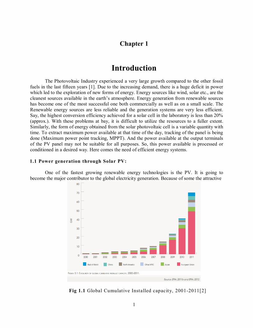
Fig 1.1 Global Cumulat ive Installed capacity, 2001-2011[2]

2
policies, the total installation capacity of PV has risen to 67.4 GW in 2011 from 1.8GW in 2000. A growth rate of 44% was registered during the past decade. And a new capacity of 27.7 GW was added in the year 2010 [2]. The cost of the system has been reduced significantly during the years.
1.2 Annual PV capacity additions: Most of the installations are from Germany and Italy. But only 0.2% of electricity
generation is from PV. Around 80% of the global demand is from the European market. Apart from these two countries, the major emerging markets are China, the Middle East, South Korea, India and other Southeast-Asian countries.
1.3 Grid Integration through the power electronic converter:
In the 90’s, most of the applications (telecommunications, rural electric supply) used to
get the power from the stand-alone PV systems. And there are a lot of grid connections available. The reduction in the overall cost of the system has led to such a change. The grid connection is possible only through a DC to AC converter which supports the interconnection of the distributed generation systems, storage systems, and renewable energy systems to the electric power system.
Grid converter is mainly a semiconductor based circuit technology which inverts the
incoming signal (i.e., AC-DC and DC-AC). The rise in power demand has led to the creation of new control methods such as more voltage levels leading to much more complex topologies. For example, a normal H-Bridge converter modified to multilevel converters or interleaved structures etc.
1.4 Outline of the Report:
The work presented in this report focuses on analyzing various transformerless
topologies for the photovoltaic systems regarding the common mode voltage and leakage current issues in the absence of galvanic isolation.
The main objective of this report is to analyze and verify the existing topologies along
with various pulse width modulation techniques which help reduce the effect of common mode voltage.

3
Chapter 2
The Transformerless Inverter Topologies The efficiency of a PV panel is close to 20% which is very less [3]. So, the PV system will be having an efficiency lesser than the efficiency of a PV panel. This is due to the losses incurred in the several stages of the entire system. The typical grid connected PV system constitutes the source, DC-DC conversion stage with maximum power point tracking stage, a DC to sinusoidal AC conversion stage and an isolation transformer at the inverter output or a high frequency transformer in the DC-DC convertor. The efficiency can be improved by either removing the transformer which will improve the efficiency by 2% [3] or improve the converter efficiency by reducing the number of stages. In this chapter, various problems associated with the transformerless converters were discussed and some of the standard topologies were discussed.
2.1 Parasitic Capacitance of the PV Arrays: The PV panel comes with a metallic frame which when charged by an external voltage signal, the metallic frame forms a capacitance with ground as the other surface and air as dielectric. So, the stray capacitance which when energized with a high frequency signal allows a significant current to pass through it. This value of this capacitance depends on various factors like: 1. Total surface area of the PV array and ground frame 2. The space between the two surfaces 3. Atmospheric conditions like dust and humidity [4] 2.2 Leakage Ground Current: In the grid connected system, the PV panel terminals will be connected directly to the grid. There is no galvanic isolation from the grid. As a result, current will flow through the parasitic capacitance which is the case in almost all the single phase transformerless inverter. Half the amplitude of the grid voltage will appear across the terminals of a PV array oscillating with grid frequency. For a three-phase system, the voltage oscillations are very less resulting in lesser leakage currents. For the safety purposes, the grid neutral is connected to the negative terminal of the DC bus. For all the neutral point clamped converters, the neutral point is connected to the neutral of the grid which is to be grounded. Depending on the PWM techniques used, a high frequency voltage may appear across the resonant circuit formed by the stray capacitances of the transistor switches, PV array and the filter inductor. As a consequence, large currents will flow in the circuit. The allowable limit for the root mean square value of the leakage current is 30mA and the peak current allowable is

4
50mA according to the German VDE0126-1-1 standard [4] and it also suggests the installation of residual current monitoring units (RCMUs). And the system should be disconnected from the grid within 0.3s after the rise. 2.2 Leakage Current analysis of a Transformerless inverter: The leakage current is found out by the simple circuit analysis wherein the equivalent network is evaluated to find the expression of current. Here, the leakage current analysis was done for a single-phase H-bridge inverter which can be done in the same fashion. The equivalent circuit of the H-Bridge inverter is shown in the figure 2.1, where L1 and L2 are the filter inductances on the phase and neutral neglecting the grid inductance. Vcm , Vdm represents the common mode voltage and the differential mode voltage of the inverter given by the expressions: Ucm = VAN + VBN (2.1) Udm = VAN – VBN (2.2)
Fig. 2.1 Simplified equivalent circuit of a H-Bridge transformerless inverter [3]
Where, VAN and VBN are the voltages across the points A and B with respect to the negative bus. The equivalent circuit derived from the H bridge circuit is shown in the figure 2.1. The equivalent voltages and the total equivalent voltages are derived in [3]. The equivalent common mode voltage is given by
Uecm = Ucm + Udmୢ୫ଶ
ିା (2.3)
If both the filter inductors possess the same value, then the common mode voltage depends only on VAN and VBN. From the circuit if the common mode voltage constant, then the current eventually die down to zero. So, it is advisable to maintain the common mode voltage constant as the current due to the grid voltage is very less compared to the common mode current. Some of the very popular topologies were discussed in the next section.

5
2.3 Transformerless Inverter Topologies: Various transformerless topologies were proposed for the elimination of leakage ground current and its effect. Of these, most of the topologies addressed the problems related to the single phase inverter because the fluctuations in the three phase system are considerably less. These topologies were classified into two types; Topologies derived from the H-Bridge topologies and, Those which are derived from neutral point clamped inverter (NPC)
2.3.1 Topologies derived from H-Bridge converter The topologies derived from the basic H-Bridge converter (Fig 2.2) are discussed below
by modifying it in order to provide a galvanic isolation. Some pulse width modulation techniques are investigated on the basis of common mode voltage and leakage current.
The topologies include: 1) H-Bridge with bipolar modulation 2) H-Bridge with unipolar modulation
Fig 2.2 Basic H-Bridge topology showing a PV source, an inverter and the grid [1]
3) H5 topology (H-Bridge with DC bypass) 4) H6 topology (H-Bridge with AC bypass or HERIC topology) 2.3.1.1 H-Bridge with bipolar modulation: In figure 2.2, the switches S1 – S2, S3 - S4 are complementary, where no two switches are on at the same time. In this topology, the common mode voltage is constant value +VPV. In bipolar pulse width modulation, the inverter output voltage varies from +VPV to –VPV. The total

6
change in the voltage is +2VPV, as a result the current ripple in the filter inductor. This results in more losses. The FFT analysis provide with information of the presence of a significant component at the switching frequency to design the filter. Though the common mode voltage is a constant, the efficiency is low due to the losses in the core. 2.3.1.2 H-Bridge with unipolar modulation: In this modulation technique, the inverter has three levels in its output voltage i.e., +VPV, 0, -VPV having a dominant harmonic component at 2fs where fs is the switching frequency used in the bipolar modulation technique. The inverter is disconnected from the grid during the zero voltage state which is obtained in two situations: S1 ON S3 ON (or) S2 ON S4 ON. The filter size reduces to half. The change in the inverter output voltage is unipolar in nature hence, reduced losses. But, the common mode voltage varies with switching frequency resulting in high leakage current. 2.3.1.3 H5 topology (H-Bridge with DC bypass): As a replacement to the transformer, an extra series switch is connected on the DC side of the inverter Fig 2.3. This inverter was proposed by SMA and named it as H5 topology for having 5 switches in it. The extra switch is used to separate the grid and the DC side of the inverter which does not allow the current to flow through the stray capacitance. The upper two switches S1 and S3 are switched with grid frequency and are complementary to each other. On the other hand, the switches S2 and S4 are switched at switching frequency when S1 and S3 are on respectively and S5 operates along with S2 during the positive half-cycle and S4 during the negative half-cycle. The inverter operates in four modes as,
Fig. 2.3 H5 topology derived from H bridge inverter by SMA [1]
Mode I: ig > 0, Vab = +VPV

7
S1 conducts continuously in the positive half-cycle, S2 and S5 are ON. The current passes through DC link voltage source, S5 - S1 - L1 - Vg – L2 - S2 and back to the DC source. Mode II: ig < 0, VAB = 0 V S1 conducts and S2 and S5 are OFF. But, the current in the inductor cannot change suddenly so the current passes through S1 – L1 – Vg – L2 - D3 – S1. During this stage, the grid is totally isolated from the inverter. Mode III: ig > 0, VAB = -VPV S3 is ON for the entire negative half-cycle. In this mode S4 and S5 are ON. The current passes through S5 – S3 – L2 – Vg – L1 – S4 – VPV(Source). In this mode the grid side elements are isolated from the DC link side. Mode IV: ig < 0, VAB = 0V S3 conducts and S4 and S5 are OFF. But, the current in the inductor cannot change suddenly so the current passes through S3 – L2 – Vg – L1 – D1 – S3. During this stage, the grid is totally isolated from the inverter. The voltage is unipolar in nature and the voltage at the DC link terminals is a sinusoidal while having the same conversion efficiency as of the unipolar modulation topology. Note: The common mode voltage during the powering mode is VPV/3 and during the free-wheeling mode, the voltage is VPV/2 which is achieved after a finite time equal to 5 times the time constant of the circuit. The Vcm is not constant which results in a significant current. 2.3.1.4 H6 with AC bypass (HERIC- Highly Efficient and Reliable Inverter concept): In 2006, this topology was patented by the Sunways by adding two switched leg on the AC side of the inverter shown in the figure 2.4
Fig. 2.4 HERIC topology derived from H bridge inverter [1]

8
Mode I: ig > 0, VAB = +VPV In this mode, switches S1 and S2 are turned on with output voltage +VPV. The voltages Van and Vbn are calculated assuming that all the switches used here are ideal.
Van = +VPV Vbn = 0V Vcm = (Van + Vbn)/2 = +VPV/2 Mode II: ig > 0, VAB = 0V, The switching of either S5 or S6 depends on the direction of the grid current. For positive grid current, switch S5 is turned on. The path of the grid current is along S5 – D6 – L2 – grid – L2 – S5. The common-mode voltage is calculated by assuming parasitic capacitance across each switch which is open. Hence, VAN = VPV/2; VBN = VPV/2. Hence, Vcm = VPV/2 Mode III: ig < 0, VAB = -VPV Switches S3 and S4 are turned on and the grid current is negative direction. S5 and S6 are open. VAN = 0V; VBN = VPV; Vcm = VPV/2.
Mode IV: ig < 0, VAB = 0V
Here S6 will be switched on and the current path is S6 – D5 – L1 – grid – L2 – S6. The common mode voltage is same as VPV. The grid current passes through two switches in the powering mode (Mode I & III) and one switch with a frequency of grid and a diode (S6, D5 or S5, D6) in the free-wheeling modes (Mode II & IV). So the switching losses in the inverter are very less compared to the other proposed topologies, hence the name Highly Efficient and Reliable Inverter Concept (HERIC). Also, the switches on the grid side isolate the DC link side during the zero voltage periods hence the name of the topology H6 with AC bypass.
2.3.2 Topologies derived the from the NPC converter
The converter topologies discussed in the previous section assumes no parasitic capacitance for the switches used. But when the inverter is switched at a very high frequency, say, 20 kHz, the effect of the stray capacitance is significant. So, during the zero voltage period these elements along with the filter inductors (grid inductance neglected) forms a resonant circuit. Due to the oscillations performed during the zero voltage stage, the point a (b) is in floating stage. At this instant, common mode voltage oscillates leading to the rise in ground leakage current. During the zero voltage modes, the voltage of midpoint of the leg ‘A’ or ‘B’ to the negative bus has to be maintained constant. This is done by connecting a switch across the

9
midpoint of the DC link and the zero voltage point. This clamps the voltage of the floating point to +VPV/2 maintaining the Vcm constant. The only disadvantage is that these topologies require two dc sources for the two capacitors. Again, efficiency of the inverter depends on the losses in the inverter. Some of the few popular topologies were discussed as follows:
1) oH5 topology 2) H-Bridge Zero voltage rectifier (HB-ZVR) 3) Full Bridge DC bypass topology (FB-DCBP)
2.3.2.1 o-H5 (Optimized H5 topology) Topology This is an optimized version of the H5 topology[4] fig. 2.5. Here, a split capacitor leg is incorporated so that the mid-point of the inverter leg is connected to it. This connection is made using an extra switch in between the points. In this way the common mode voltage is maintained constant.
Fig. 2.5(a) An optimized version of H5 topology – oH5 topology [4]
Mode I: ig > 0, Vg > 0; A small dead time has to be provided between the switching instants of the series switch (S5) and the clamping switch (S6). Otherwise, Cdc1 will be closed by a very low impedance path (short-circuit) which will damage the source. In this mode, when both the grid current and voltage are same, switches S1, S2 and S5 are on. And the inverter voltage will be VPV. The grid current slowly rises to its maximum and then starts falling down similar to the grid voltage. S6 is kept open. The current path is CPV1 – S5 – S1 – L1 – Vg – L2 – S3 – CPV2. The common mode voltage equals +VPV/2. Mode II: ig > 0, Vg = 0; All the switches are open and S6 is closed small time after switch S5 is open in order to avoid any damage to the device. At this instant, when S6 is closed the voltage V3N and V4N are clamped to +VPV/2 resulting in Vcm = VPV/2. If the voltages at the points A, B are greater than
10
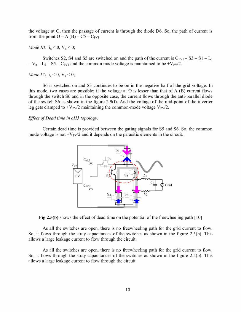
the voltage at O, then the passage of current is through the diode D6. So, the path of current is from the point O – A (B) – C5 – CPV1. Mode III: ig < 0, Vg < 0; Switches S2, S4 and S5 are switched on and the path of the current is CPV1 – S3 – S1 – L1 – Vg – L2 – S5 – CPV1 and the common mode voltage is maintained to be +VPV/2. Mode IV: ig < 0, Vg < 0; S6 is switched on and S3 continues to be on in the negative half of the grid voltage. In this mode, two cases are possible; if the voltage at O is lesser than that of A (B) current flows through the switch S6 and in the opposite case, the current flows through the anti-parallel diode of the switch S6 as shown in the figure 2.9(f). And the voltage of the mid-point of the inverter leg gets clamped to +VPV/2 maintaining the common-mode voltage VPV/2. Effect of Dead time in oH5 topology: Certain dead time is provided between the gating signals for S5 and S6. So, the common mode voltage is not +VPV/2 and it depends on the parasitic elements in the circuit.
Fig 2.5(b) shows the effect of dead time on the potential of the freewheeling path [10] As all the switches are open, there is no freewheeling path for the grid current to flow. So, it flows through the stray capacitances of the switches as shown in the figure 2.5(b). This allows a large leakage current to flow through the circuit. As all the switches are open, there is no freewheeling path for the grid current to flow. So, it flows through the stray capacitances of the switches as shown in the figure 2.5(b). This allows a large leakage current to flow through the circuit.

11
2.3.2.2 H-Bridge Zero Voltage Rectifier (HB - ZVR) Another way of limiting the leakage current by keeping the common mode voltage constant is by inserting an extra power-electronic switch with a diode bridge rectifier as shown in the figure 2.10. The grid is isolated from the source from the AC side. So, this method is proposed for AC decoupling. The bi-directional diode bridge is clamped to the mid-point of DC link capacitor using a diode. The decoupling element is shown in the figure 2.6.
Fig. 2.6 H-Bridge Zero Voltage Rectifier (HB - ZVR) [3]
The positive vector is achieved by switching S1-S2 and negative vector by S3-S4. The zero-vector is achieved by switching on the S5 by providing a small dead time of 2µs to avoid short-circuit of the input capacitor. During the zero states, current passes through the diodes of the bridge rectifier and the S5. During the dead time all the switches would be in OFF state, which allows the free-wheeling current to flow through the parasitic capacitance of the switches into the DC link capacitors. The peak current in this topology is greater than 50ms. The current during the zero voltage free cycles across the bridge rectifier. During the dead time, the time duration between the zero voltage stage and the active stage, the grid current find a way through two diodes which incurs more losses. Hence, this topology is less efficient than the HERIC topology. Also six extra diodes are incorporated for implementing this topology 2.3.2.3 Full Bridge DC bypass topology (FB-DCBP) Fig. 2.7 shows the proposed topology which consists of six switches, of them, two switches are connected in series on the either side of the DC link. The blocking voltage of the switches S1 and S2 are halved due to the capacitor divisor formed by the diodes. Hence, the saturation voltages are reduced. This inverter topology can also inject power with cosφ other than unity.

12
Fig. 2.7 Full Bridge PV bypass topology (FB-DCBP) [3]
Modes of Operation: The output of the inverter produced is a three level voltage with considerable conduction losses compared to the other NPC topologies. Mode I: In the positive half cycle of the grid voltage, switches S1 and S4 are switched on. The switches S5 and S6 are switched at switching frequency. The switches S2 and S3 are switched complementary to the switches S5-S6. This mode produces an active voltage vector +VPV. And Van = +VPV and Van = 0 V. Hence, Vcm = VPV/2. Mode II: In the free-wheeling mode, the voltage VAB = 0 V and the switches S3 and S2 will be conducting along with S1-S4. So, all the four switches will be conducting, The inductor current freewheels through the diodes D2 - D3 and the switches S1 – S4. So, the conduction loss is limited to only two switches. Mode III and Mode IV have the similar operation in the negative half of the grid voltage. The roles of S1 - S4 and S2 – S3 gets interchanged The efficiency of this inverter is very less due to the conduction of four switches during the active voltage vector. But even this topology is reducing the oscillations in the common mode voltage. 2.3.3 Half Bridge Topologies
The half-bridge converter shown in the figure fig. 2.8 uses two switches to do the dc-ac
conversion by connecting to either the negative or the positive bus wherein the neutral is always

13
Fig. 2.8 Typical Half Bridge inverter [3]
connected to the middle point of the capacitors. The main disadvantage is the usage of two dc sources whereas the H-Bridge topology
requires only one source. Also the voltage rating of each switch should be twice that of the H-Bridge topology. But the output voltage is bipolar in nature which generates a constant common mode voltage. So, this topology is suitable as a transformerless topology, but source voltage of 1000V or more is practically not available. So this option is not viable.
2.3.4 Comparison of Various Transformerless Topologies The consumer buys a product by searching for its pros and cons of it. Then he will compare all the variants available in the market and make the best choice out of them. Similarly, the various transformerless inverters are compared on the basis of their cost, efficiency, common-mode voltage and the leakage current characteristics by the following table. Table 2.1 Comparison among various topologies which are derived from H-Bridge and NPC
Topology
Type of Inverter
output (Unipolar/Bipolar)
O/P Voltage Levels
No. of Devices Conducting
(S/D)
Constant Common-
mode Voltage (Y/N)
Efficiency
Active Free
Wheeling (order)
H-Bridge Bipolar 2 2/0 - Y 6 H-Bridge Unipolar 3 2/0 1/1 N 4
H-5 Unipolar 3 3/0 1/1 N 5 HERIC Unipolar 3 2/0 1/1 Y 1
oH5 Unipolar 3 3/0 1+1*/1+1* N 3 HB-ZVR Unipolar 3 2/0 1/2 Y 2
HB-DCBP
Unipolar 3 4/0 2/2 Y 7
(* Note: The number represents either a diode or a transistor switch)

14
Chapter 3
Improved H6 – DC Bypass NPC Topology
The NPC topology aims at maintaining constant common mode voltage even during the freewheeling mode of operation. Various topologies derived from NPC such as oH5, HB – ZVR and HB – DCBP were discussed in the previous chapter. A new topology was derived from the H6 – DCBP topology by shifting the switch S6 from the negative DC bus. The branch consisting of switch S6 is connected to the mid-point of the DC link and the point B with the help of a diode as shown in the figure 3.1.
Fig. 3.1 Modified H6 Neutral Point clamped PV bypass Transformerless Topology
The various modes of operation are discussed in detail in absence of parasitic elements. The switches S1-S6 are operated at grid frequency in the positive half cycle of grid current. Also, S3 is operated at grid frequency but complementary to the S1-S6 pair. Extra diodes D+ used to protect the source from short-circuiting and D- used to clamp the freewheeling path to +VPV/2. Modes I and II are related to the inverter operation in the positive half cycle of the grid current. And, Modes III and IV are discussed for the grid current in its negative half – cycle. 3.1 Modes of Operation: Mode I: Vg > 0, ig > 0, The switches S1, S2, S5 and S6 are switched on so that the voltage across the inverter output terminals VAB = +VPV. The path of current is along CPV1/2 – S5 – S1 – L1 – grid – L2 – S2 – CPV2 – CPV1 (fig 3.2). Even though S6 is kept on, the current does not flow through it as the diode D- is reverse biased by the voltage across CPV2. The voltages VAO = VPV and VBO = 0 V. The common mode voltage is given by (VAO + VBO)/2 = VPV/2.

15
Fig 3.2 The operation of improved H6-DCBP topology under Mode I Mode II: VAB = 0 V, ig > 0, The switches S1 and S6 remains in the on position but the switches S2, S5, S3, S4 are switched off. The path for the freewheeling current is along S1 – L1 – grid – L2 – D3 – S3. A part of the freewheeling current flows through the diodes D- - CPV2 – D2. ig = iD- + iD3 (3.1) VAO = VPV/2, VBO = VPV/2 (3.2) So, the common mode voltage is the average of both the voltages VAO and VBO given by, Vcm = +VPV/2 (3.3) During the powering mode, the potential at A with respect to O is VPV and that of B is 0V. When the grid is disconnected from the inverter PV side, the potential at A starts falling and the potential at the point B starts rising. As a result of some parasitic elements in the circuit, the potentials start oscillating. When the potential of B is greater than the potential at O, then the voltage of the freewheeling path gets clamped to VPV/2 equal to the common mode voltage. Mode III: VAB = -VPV, ig < 0, Switches S3, S4, S5 are switched on and the remaining switches are kept in off position. The switch S6 should be switched in complementary with S5. Both S5 and S6 should be switched with a small dead time in between their gating signals. Otherwise, it will damage the CPV1 source.

16
Fig. 3.3 Mode II operation, the freewheeling mode
Fig. 3.4 Path showing the direction of grid current in the negative half cycle
Fig. 3.5 The grid current during the freewheeling period and the clamping current
through D- and CPV2 in Mode IV Mode IV: VAB = 0V, ig < 0,

17
Similar switching pattern was followed here, S3 and S6 are switched on and remaining are switched on (See Fig. 3.5). The phenomenon of voltage clamping happens as explained in the Mode II. Hence, the common mode voltage gets fixed to +VPV/2. 3.2 Simulation Results: The operation of the proposed topology was verified by simulation it in MATLAB/SIMULINK. The following figures show the plots of Grid current, Grid Voltage, Common mode voltage and Leakage current. 3.2.1 Ground Leakage Current and Common mode Voltage: The rms value of leakage current is 19mA which is well under the limits.
Fig. 3.6 Common mode voltage and ground leakage current
3.2.2. Voltages across the stray capacitances at the negative and positive bus of the inverter:
Fig 3.7 The voltages of the positive PV bus and negative PV bus w.r.t ground

18
Chapter 4
Conclusions and Future Work
The transformerless topologies were analyzed on the basis of common mode voltage and ground leakage current. The two basic pulse width modulation techniques namely, Bipolar and Unipolar pulse width modulation techniques for H-Bridge inverter were discussed along with their advantages and disadvantages for incorporating them in the transformerless photovoltaic systems connected to the grid.
Various topologies derived from the H bridge inverter were discussed which are suitable for the requirement. Comparisons were made with respect to the common mode voltage and losses in the inverter system. Some of the very popular topologies were discussed in detail and verified the topologies in MATLAB®/SIMULINK.
4.1 Limitations and Future Work:
The topologies were verified by assuming that the power is injected into the grid at unity
power factor. Issues related to the operation other than unity power factor is not considered here. The voltage across the capacitors was taken to be constant while performing the
simulations and only the current control was done. Also, the parasitic nature of the switches was neglected while simulating various topologies.
The new topology based on the NPC topology needs to be verified considering the device
parasitic and the efficiency calculations are yet to be made. Simulation results will be verified through hardware experimentation for the new
topology and the results would be analyzed and compared with the existing topologies.

19
References
[1] Remus Teodorescu, Liserre M., “Grid connected converters for Photovoltaic and wind power
systems”, John Wiley and Sons, The Atrium, Southern Gate, Chichester, West Sussex, UK,
2011.
[2] IRENA working paper, Renewable energy technologies: Cost Analysis series, Vol.1: Power
sector Issue 4(5), Solar photovoltaics.
[3] Bo Yang, Li W., Gu Y., Cui W., He X., “Improved Transformerless Inverter With
Common-Mode Leakage Current Elimination for a Photovoltaic Grid-Connected Power
System”, IEEE Transactions on Power Electronics, Vol. 27, No. 2, Feb. 2012, pp. 752-762.
[4] Anandbabu Ch., Fernandes B. G., “Improved Full-Bridge Neutral Point Clamped
Transformerless Inverter for Photovoltaic Grid-Connected System”, Industrial Electronics
Society, IECON 2013 - 39th Annual Conference of the IEEE , vol., no., pp.7996,8001, 10-13
Nov. 2013
[5] Tamás Kerekes, “Analysis and Modeling of Transformerless Photovoltaic Inverter Systems”,
Ph. D. Thesis, Institute of Energy Technology, Aalborg University, Denmark, 2009.
[6] M. Calais and V. Agelidis; “Multilevel converters for single-phase grid connected
photovoltaic systems, an overview”, IEEE – International Symposium on Industrial Electronics,
7-10 Jul. 1998, pp. 224-229.
[7] Li Zhang, Kai Sun, Lanlan Feng, Hongfei Wu, Yan Xing, “A Family of Neutral Point
Clamped Full-Bridge Topologies for Transformerless Photovoltaic Grid-Tied Inverters”, IEEE
Transactions on Power Electronics, Vol. 28, No. 2 Feb. 2013, pp. 732-739.
[8] González R., López J., Sanchis P., Luis M., “Transformerless Inverter for Single-Phase
Photovoltaic Systems”, IEEE Transactions on Power Electronics, Vol. 22, No. 2, Mar. 2007, pp.
693-697.
[9] Kerekes T., Teodorescu R., Rodríguez P., Vázquez G., Aldabas E., “A New High-Efficiency
Single-Phase Transformerless PV Inverter Topology”, IEEE Transactions on Power Electronics,
Vol. 58, No. 1, Jan. 2011, pp. 184-191.
[10] Li Zhang, Sun K., Xing Y., Xing M., “H6 Transformerless Full-Bridge PV Grid-Tied
Inverters”, IEEE Transactions on Power Electronics, Vol. 29, No. 3, pp. 1229-1238.
Related Documents