~y~er Optical Interconnect T e c ~ n o l o ~ y ( ac~aging and interconnect for Board and e Applications Y. S. Liu, R.J. Wojnarowski and W.A. Hennessy GE Corporate Research & Development Center, Schenectady, NY 12301 J. P. Bristow, Yue Liu and A. Peczalski Honeywell Technology Center, Minneapolis, MN 55418 J. Rowlette, A. Plotts, J. Stack and M. Kadar-Kallen AMP, Optical Interconnect Systems, Harrisburg, PA 17105 J. Yardley and L. Eldada AlliedSignal Research & Technology Center, Morristowm, NJ 07960 R.M. Osgood and R. Scarmozzino Columbia University, New York, NY 10027 S.H.Lee, V. Ozgus and S. Patra UCSD, La Jolla, CA., 92093 Key words: optical interconnect, optoelectronic packaging, high speed optical links, backplane and board level interconnect, VCSEL packaging, polymer waveguide, Polyguide The Polymer Optical Interconnect Technology (POINT) is a collaborative program among GE, Honeywell, AMP, AlliedSignal, Columbia University and University of California at San Diego (UCSD), sponsored by ARPA, in developing affordable optoelectronic packaging and interconnect techno~ogies for board- and backplane- level optical interconnect applications. The POINT program leverages on the existing electronic design, processing, fabrication and MCM packaging technologies to optoelectronic packaging. The POINT program also incorporates several state-of-the-art optoelectronic technologies that include: high speed VCSEL for multi-channel data transmission; flexible optical polymer waveguides and low-loss polymers for board and backplane interconnects; low-cost diffractive optical elements (DOE) for board-to-backplane interconnect; and use of molded MT-type connectors to reduce weight and size. In addition, to further reduce design and fabrication cycle times, CAD tools for multimode optical waveguide modeling, and for mechanical modeling of optoelectronic packaging will be employed to aid the technology development. The rapid advance in the processor speed and processing power in recent years has dramatically increased the data transfer rates between modules, board, backplane and cabinets. In the advanced high performance computing systems, interactive multimedia and high speed switching network communication systems, data transf~rrates are exceeding several Gbps. The optical ~n~erconnec$ technology offers higher data bandw~dch, creased ID density, reduced crosstalk, ease of impe insensitive to EMI, and reduced weight and size of cabling. The deployment of optical interconnect in the telecommunication industry since 70’s has not only successfully demonstrated these technical merits, more significantly, it has led to the dramatic reduction of the cost of communication and made a profound impact on how people communicate. The applications of optical interconnect in advanced computers and communication systems, however, have been hindered by relatively high costs of optoelectronic components, modules, connectors, and the transmission media for relatively short distance communication from c 100 meters (for cabinet to cabinet) to less than meters (for between modules and boards). To a large extent, the lack of a common packaging platform between the optoelectronic devices and those used for electronic components is a key technical roadblock. The demand for higher data transfer rates and the increasing complexity and costs in finding electrical solutions for intra- and inter-cabinet interconnect have led to several major laboratory activities worldwide to develop optical interconnect into a viable alternative to the copper solution. 1-7 0-7803-3286-5/96 $4.00 01996 IEEE 308 1996 ElectronicComponentsand Technology Conference

Welcome message from author
This document is posted to help you gain knowledge. Please leave a comment to let me know what you think about it! Share it to your friends and learn new things together.
Transcript
~ y ~ e r Optical Interconnect T e c ~ n o l o ~ y ( ac~aging and interconnect for Board and e Applications
Y. S. Liu, R.J. Wojnarowski and W.A. Hennessy GE Corporate Research & Development Center, Schenectady, NY 12301
J. P. Bristow, Yue Liu and A. Peczalski Honeywell Technology Center, Minneapolis, MN 55418
J. Rowlette, A. Plotts, J. Stack and M. Kadar-Kallen AMP, Optical Interconnect Systems, Harrisburg, PA 17105
J. Yardley and L. Eldada AlliedSignal Research & Technology Center, Morristowm, NJ 07960
R.M. Osgood and R. Scarmozzino Columbia University, New York, NY 10027
S.H.Lee, V. Ozgus and S. Patra UCSD, La Jolla, CA., 92093
Key words: optical interconnect, optoelectronic packaging, high speed optical links, backplane and board level interconnect, VCSEL packaging, polymer waveguide, Polyguide
The Polymer Optical Interconnect Technology (POINT) is a collaborative program among GE, Honeywell, AMP, AlliedSignal, Columbia University and University of California at San Diego (UCSD), sponsored by ARPA, in developing affordable optoelectronic packaging and interconnect techno~ogies for board- and backplane- level optical interconnect applications. The POINT program leverages on the existing electronic design, processing, fabrication and MCM packaging technologies to optoelectronic packaging. The POINT program also incorporates several state-of-the-art optoelectronic technologies that include: high speed VCSEL for multi-channel data transmission; flexible optical polymer waveguides and low-loss polymers for board and backplane interconnects; low-cost diffractive optical elements (DOE) for board-to-backplane interconnect; and use of molded MT-type connectors to reduce weight and size. In addition, to further reduce design and fabrication cycle times, CAD tools for multimode optical waveguide modeling, and for mechanical modeling of optoelectronic packaging will be employed to aid the technology development.
The rapid advance in the processor speed and processing power in recent years has dramatically increased the data transfer rates between modules, board, backplane and cabinets. In the advanced high performance computing systems, interactive multimedia and high speed switching network communication systems, data t ransf~r rates are exceeding several Gbps. The optical ~n~erconnec$ technology offers higher data bandw~dch, creased I D density, reduced crosstalk, ease of impe insensitive to EMI, and reduced weight and size of cabling. The deployment of optical interconnect in the telecommunication industry since 70’s has not only successfully demonstrated these technical merits, more significantly, it has led to the dramatic reduction of the cost of communication and made a profound impact on how people communicate.
The applications of optical interconnect in advanced computers and communication systems, however, have been hindered by relatively high costs of optoelectronic components, modules, connectors, and the transmission media for relatively short distance communication from c 100 meters (for cabinet to cabinet) to less than meters (for between modules and boards). To a large extent, the lack of a common packaging platform between the optoelectronic devices and those used for electronic components is a key technical roadblock. The demand for higher data transfer rates and the increasing complexity and costs in finding electrical solutions for intra- and inter-cabinet interconnect have led to several major laboratory activities worldwide to develop optical interconnect into a viable alternative to the copper solution. 1-7
0-7803-3286-5/96 $4.00 01996 IEEE 308 1996 Electronic Components and Technology Conference

D
interconnect ~ e c ~ m o ~ o ~ y
The POINT t m was organized to develop affordable optoelectronic packaging and interconnect technologies for board- and backplane- level optical interconnect applications. It is a collaborative effort e
among GE, Honeywell, AMP, AlliedSignal, Columbia University and UCSD, sponsored by ARPA. The approach of the POINT program is to leverage the standard planar and batch processes already employed in the electronic industry and apply them to optoelectronic packaging to accelerate the integration of optoelectronic and electronic interconnects on board- and backplane levels. The organization, the . principal investigator of each Team member, and the respective responsible technical areas are illustrated in Fig. 1. The POINT team leverages the technical expertise of each individual Team member in the following areas: . * Optoelectronic packaging technology- A high
performance thin film multichip module (MCM) technology is used to package both optoelectronic and electronic components.
Qptical polymer techno - Several state-of-the- art optical polymers employed as flexible interconnect media for module, board and backplane interconnect, e.g. by DuPont, ~ O W - ~ O S S optical polymer by A ~ ~ i ~ d S i g n a ~ ~ and P o l y e ~ ~ e r i m i d e / ~ ~ ~ by GE/Mone ywell.
Low-cost manufacturable assembly technolog~es and companents- Planar and batch processes are used for optoelectronic packaging and passive alignment processes are employed to reduce optoelectronic assembling costs. VCSEk arrays are scaleable to large volume and low-cost manufacturing.
Key interface components- MT-type connectors are used between Polyguide and fiber ribbons, and diffractive optical elements (DOE) are used for board to backplane interconnects.
Computer simulation tools- simulation tools are ultilized to aid the design of multimode optical waveguides and to model mechanical and thermal performances of optoelectronic packaging assemblies.
VCSELs, receivers, electronic components d backplane optical interconnect demo.
Fig. 1. The organization, principal investigator of each team member and the respective responsible technical areas.
309 1996 Electronic Components and Technology Conference
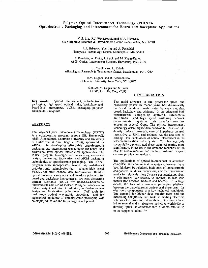
POINT backplane will demonstrate capability of 4-1 Ox density improvement at >500 Mbps/line
Ultem/BCB Material
Flex Polymer to Circuit Board
or Fiber Connector Other Cabinets
-~ - __ ~ ~. ~ --- -- ~ -
Fig. 2 summarizes the scope of technology development under the POINT program.
to
Fig. 2 summarizes the scope of technology development under the POINT program. This paper will describe some of the progress made to date and selected on-going activities of the POINT program. The first phase of this program is to develop 4-channel optoelectronic transmitter and receiver for building board and backplane interconnect test assembly. These transmitters and receivers will also be used for demonstration of a novel packaging technology for surface emitting devices such as VCSEL and receivers to be described in the following sections.
3. Vertical cavity surface-emitting lasers (VCSEL):
VCSEL devices represent a significant component development for optical interconnect applications and
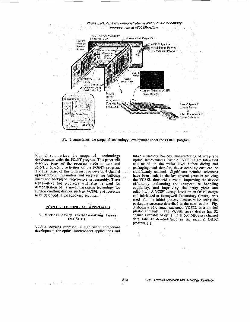
make ultimately low-cost manufacturing of array-type optical interconnects feasible. VCSELs are fabricated and tested on the wafer level before dicing and packaging, and therefor, the assembling cost can be significantly reduced. Significant technical advances have been made in the last several years in reducing the VCSEL threshold current, improving the device efficiency, enhancing the temperature handling capability, and improving the array yield and reliability. A VCSEL array, based on an OETC design and fabricated at Honeywell Technology Center, was used for the initial process demonstration using the packaging structure described in the next section. Fig. 3 shows a 32-channel packaged VCSEL in a molded plastic substrate. The VCSEL array design has 32 channels capable of operating at 500 Mbps per channel data rate as demonstrated in the original OETC P”m. r 11
31 0 1996 Electronic Components and Technology Conference
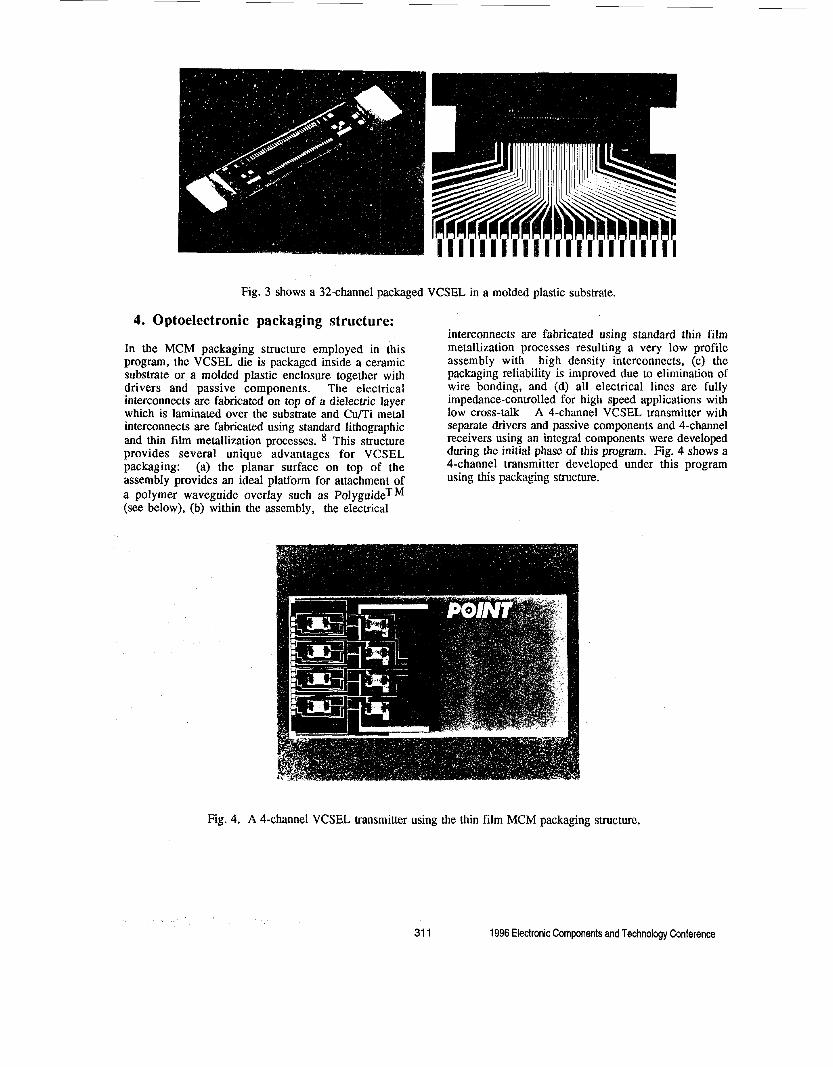
Fig. 3 shows a 32-channel packaged VCSEL in a molded plastic substrate.
4. Optoelectronic packaging structure:
In the MCM packaging structure employed in this program, the VCSEL die is packaged inside a ceramic substrate or a molded plastic enclosure together with drivers and passive components. The electrical interconnects are fabricated on top of a dielectric layer which is laminated over the substrate and Cu/Ti metal interconnects are fabricated using standard lithographic and thin film metallization processes. * This structure provides several unique advantages for VCSEL packaging: (a) the planar surface on top of the assembly provides an ideal platform for attachment of a polymer waveguide overlay such as PolyguideT (see below), (b) within the assembly, the electrical
interconnects are fabricated using standard thin film metallization processes resulting a very low profile assembly with high density interconnects, (c) the packaging reliability is improved due to elimination of wire bonding, and (d) all electrical lines are fully impedance-controlled for high speed applications with low cross-talk A 4-channel VCSEL transmitter with separate drivers and passive components and 4-channel receivers using an integral components were developed during the initial phase of this program. Fig. 4 shows a 4-channel transmitter developed under this program using this packaging structure.
Fig. 4. A 4-channel VCSEL transmitter using the thin film MCM packaging structure.
31 1 1996 Electronic Components and Technology Conference

5 Polymer waveguides - flexible media for board and backplane interconnects:
The successful implementation of optical interconnect for telecommunication was attributed to a large extent the development of the low-loss optical fibers. For board and backplane applications, polymer materials offer advantages of routing flexibility and process compatibility to electronic packaging. Several optical polymers with optical loss of 0.2-0.3 dB/cm in the spectral ran e of 0.8 - 1.5 um have been reported
been reported by photolithographic processes and by dry etching processes. Efficient coupling between the channeled waveguides and VCSEL or receiver arrays through 45-degree waveguide reflectors has also been demonstrated. Z3 This coupling scheme offers a low- profile assembly. In the current program, three types of polymers are under evaluation: e.g. Polyguide developed by DuPont , low-loss polymers by AlliedSignal and polyetherimide (UltemTM)/BCB waveguide structures jointly developed by GE/Honeywell. Table 1 summarizes the optical and physical properties of these polymers.
Polyguide, developed by DuPont and licensed to AMP, has shown excellent layer quality and thickness contr01.~ Buried waveguide circuitry can be formed
recently 9*1 1 . Low loss channeled waveguides have
with low optical losses using photolithographic patterning and lamination techniques. In addition, Polyguide can be machined using excimer lasers to form mechanical structures with high degree of accuracy to place on the module, and can be connectorized to MT-type ferrule packaged with push/pull housing connected to a multi-channel standard ribbon fiber.
Another type of optical polymer is the acrylate-based polymer developed at Allied Signal and has shown extremely low optical loss (e.g. e 0.1 dB/cm at 0.8 um). 10 Because of its low-loss, it is an attractive waveguide material for backplane applications. Multimode waveguides with a dimension of 65 um x 65 um have been fabricated using laser direct patterning with an excellent sidewalls control. This polymer material can be fabricated on a variety of substrates and interfaced directly to micro-optical elements and fiber-to-waveguide interconnect structures. Fig. 5 shows a waveguide structure fabricated over a VCSEL array (left photo) in the AlliedSignal polymer using laser direct patterning and micro-optical structures including a 90-degree abruptly terminated waveguide (middle) and a 45-degree micro-reflector (right).
Table 1 Optical polymers under investigation in the POINT program and their selected optical and physical properties.
31 2 19% Electronic Components and Technology Conference

VCSEL array 90" terminated waveguide 45" end-faced waveguide
Fig. 5 shows waveguides over a VCSEL array fabricated in AlliedSignal polymer using laser direct writing (left photo), and micro-optical structures including a 90-degree abruptly terminated end face (middle), and a 45-degree micro-reflectors (right).
Polyetherimide (Ultem TM ), has been developed as a core material for waveguide fabrication., combined with benzocyclobutene (BCB) used as the cladding material. Ultem is a engineering thermoplastic with excellent temperature and mechanical stability, and has good o tical transmission properties in near 1R.l Both UltemrM and BCB materials exhibit low optical losses at 0.8-um and are compatible with the module fabrication processes. Optical waveguides have been fabricated using RIE and laser ablation methods. Optical losses of 0.2 dB/cm have been measured. l2
Fig. 6 shows a multimode waveguide array using the BCB/Ultem/BCB structure with 45-degree miero- mirrors fabricated on top of a MCM module. Using this structure, waveguide ribbons have also been fabricated on a flexible Kapton film and laminated onto a standard PWB substrate without introducing additional optical losses. This structure have been used as an interface between the board and MCMs with about 1 dB coupling loss. l 3
Fig. 6 shows a waveguide array using the BCB/Ultem/BCB structure with 45-degree micro-mirrors.
31 3 1996 ~ ~ ~ ~ r o n i c Components and ~ e c h n ~ l o ~ y C o ~ ~ ~ r e n ~

6. Process integration and passively alignment:
Since optical alignment contributes to a large fraction of the total packaging cost in an optoelectronic assembly, this program emphasizes on the development of passive alignment processes and several such techniques are currently being developed and evaluated. As an example, a passive alignment process was developed for Polyguide by placing the alignment pedestals on the assembly surface at the locations in reference to the optoelectronic component
Dual Ribbon Chicklet Interface . . . . . . . . . . . . . . .
fiducial marks. Efficient optical coupling between a Polyguide waveguide array and a VCSEL array using this assembling and passive alignment technique has been demonstrated. Fig.7 shows schematically this passive alignment process developed for Polyguide placement on an optoelectronic VCSEL package, and the measured optical outputs from a Polyguide as functions of the Polyguide displacements with respect to the VCSEL position.
Optical Coupled Power Alignment Sensitivity
Fig.7 shows schematically a passive alignment process developed for Polyguide placement onto an optoelectronic VCSEL assembly, and the measured optical outputs from a Polyguide as functions of the Polyguide displacements with respect to the VCSEL position.
The POINT program is a collaborative effort among GE, Honeywell, AMP, AlliedSignal, Columbia University and UCSD, sponsored by AFWA, to develop affordable optoelectronic packaging and interconnect technologies for board- and backplane- level optical interconnect applications. We have described some of the on-going activities during the initial phase of this program including the demonstration of a novel optoelectronic packaging technology for surface emitting devices using a thin-film MCM technology, and efficient coupling of
VCSEL to polymer waveguides via 45-degree micro- mirrors. More significantly, the optoelectronic packaging technology we have demonstrated for VCSEL and receiver arrays is adopted from and fully compatible with the planar and batch fabrication processes used in the IC industry. The current on-going effort of this program is to address the issues of optical interconnect between the board and backplane levels such as interconnect density, interconnect efficiency and reliability and to develop the required components and waveguide structures.
31 4 1996 Electronic Components and Technology Conference

This work is supported by ARPAETO (Dr. Anis Husain), and the program is managed by Wright Laboratory, USAF, (Dr. James Grote) under the conbract number F33615-94-C- 1530.
1. Y.M. Wong et al, "Technology development of a high density 32-channel 16 Gbps optical data link for uptical interconnect applications for the optoelectronic technology Consortium (OETC)," IEEE Jour. of Lightwave Tech., 1995.
2. Y.S.Liu, H.S.Cole, J.P.Bristow and Yue Liu, "Polymer-based optical interconnect technology: a route to low-cost optoelectronic packaging and interconnect," in Optical Interconnect 111, ed. by R.Chen, SPIE, p. 80, 1995.
3. Y.S.Liu, H.S.Cole, R. Guida, T, Sitnik, E.W.Balch, J. Bristow and Yue Liu, "Optoelectronic packaging and polymer waveguides for multichip module and board- level optical interconnect applications," 45th, ECTC, pp. 185-188, 1995.
4. J. Bristow, C. Sullivan, S . Mukherjee, Yue Liu and A. Husain, "Progress and status of guided wave optical interconnect technology," in "Optical Interconnects,", ed. by R. Chen, Vol. 1849, Proc. SPIE, pp. 4-10, (1993)
5. W.S. Ishak, K.H. Hahn, B.L.Booth, E..H. Mueller, A.A.J. Levi, R.R.Craig, "Optical interconnects: the
31 5
Parallel Optical Links Organization (POLO) approach," in "Optical Interconnect 111," p. 214, 1995.
6. K.H. Hahn, "POLO-Parallel optical links for Gigabyte interconnect," 45th ETCT, pp.368-375, 1995.
7. D.B. S c h w a , et, al., "A low cost high performance optical interconnect," 45th, ECTC, pp. 376-379, 1995.
8. Y.S. Liu, "Laser metal deposition for high density interconnect," in "Optics and Photonics News," Optical Society of America, p. 10. June. 1992.
9. B.L. Booth, "Polymers for integrated optical waveguides," in Polymers for electronics and photonic applications, ed by C.P. Wong, Academic Press, p.549, 1993.
10. J.T. Yardley, "Design and Characterization of organic waveguides for passive and active optical devices," in Science and Technology of Organic thin films for waveguiding nonlinear optics, ed. by F. Kajzar and J.D. Swalen, 1994.
12. H.R. Philipp, D.G. LeGrand, H.S.Cole and Y.S.Liu, "The optical properties of a polyetherimide," in "Polymer Engineering and Science," Vol. 29, No.22, p. 1574,1989.
13. J. P.Bristow, Yue Liu, T. Marta, S . Bounnak, K. Johnson, Y.S. Liu and H.S. Cole, "Cost-effective optoelectronic packaging for multichip modules and backplane level optical interconnects," in Optical Interconnect 111, SPIE, p. 61, 1995
1996 Electronic Components and Technology Conference
Related Documents