PN JUNCTION THEORY 1 Prof. Philippe LORENZINI Polytech-Nice Sophia

Welcome message from author
This document is posted to help you gain knowledge. Please leave a comment to let me know what you think about it! Share it to your friends and learn new things together.
Transcript
PN JUNCTION THEORY
1
Prof. Philippe LORENZINIPolytech-Nice Sophia

PN Homojunction• Non linear device• rectifier devices (composants redresseur)• 2 devices reach the same results:
• PN Junction(this chapter)• Schottky barrier or Metal / SC contact (next chapter)
2

The Junction’s formation mechanism
3
Flat Fermi level: No current / thermal equilibrium
•PN Junction at equilibrium1st Step: diffusion mechanism
2nd Step: built in Electric Field appears compensates diffusion forces
E int
e-h pair’srecombination
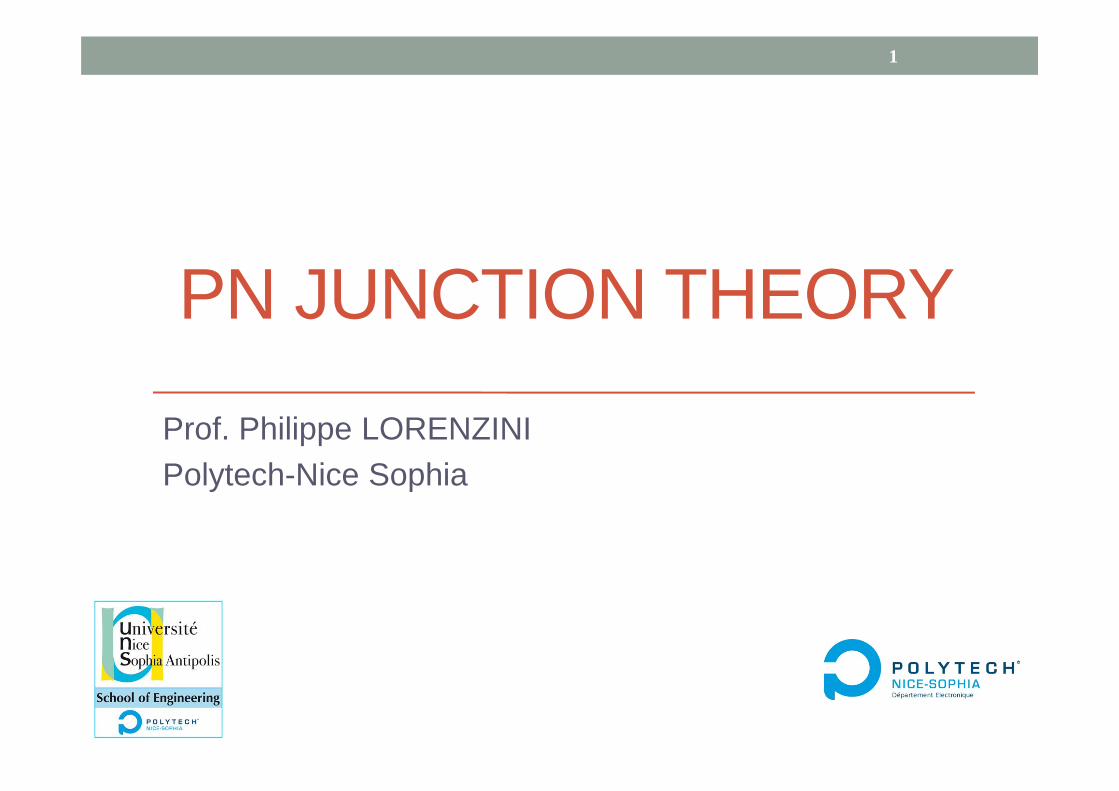
« built in potential VB i»
4
• Definition : Potential drop between N and P regions
PNbi VVV
0)()()()(
dxxdpDxExpexJ pPP
dxxdp
xpxE
Dp
p )()(
1)(
dxxdp
xpdxxdV
kTe )(
)(1)(
)ln(n
pbi p
pe
kTV
Holes current equation:
or or
Integrating from P to N region:
finally: )nNN(
ekTVV
i
DAbiD 2ln )
nNN(
ekTVV
i
DAbiD 2ln

•Field, potential and Space Charge width(1)• Poisson’s equation:
5
sc
xdx
xVd )()(
2
2
In N and P region:
Dsc
Nedx
xVd
2
2 )(NWx0
Asc
Nedx
xVd
2
2 )( 0 xWP
-WP -WN

6
Electric Field E(x)
)()( Nsc
Dn WxeNxE
)()( P
sc
AP WxeNxE
Continuity of Field on x=0:
PAND WNWN
sc
PA
sc
NDM
WeNWeNE
-WP -WN
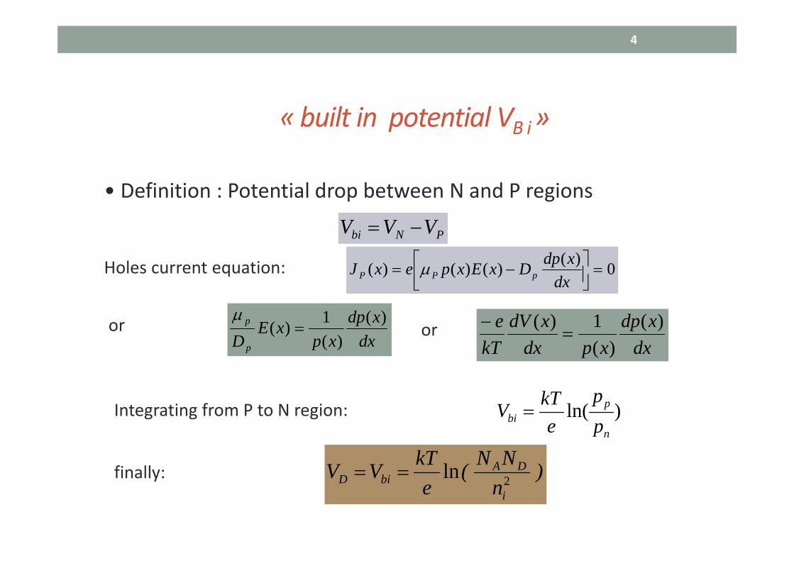
•Field, potential and Space Charge width(2)
7
Built in potential V(x)
nNsc
Dn VWxeNxV 2)(
2)(
pPsc
Ap VWxeNxV 2)(
2)(
Depletion layer (ZCE)
sc
pA
sc
nDdpn
WeNWeNVWVWV
22)()(
22
dDAA
Dscdp V
NNNN
eVW
)(2
)(
dDAD
Ascdn V
NNNN
eVW
)(2)(
dDA
ADscd V
NNNN
eVW
2)( -WP WN
•Field, potential and Space Charge width(3)

WARNING: WHEN A VOLTAGE V ISAPPLIED ON P SIDE, VBI HAVE TO
BE REPLACED BY VBI - V
8
BIASED PN JUNCTION
• When a positive voltage is applied on p side, the equilibrium is destroyed and a net current can flow
9
simplifying assumptions : Depletion layer with no free carriers (e‐ and h+) Low injection Boltzmann’s approximation Drop voltage only in depletion layer No generation‐recombination mechanisms present

• Foward Biasing• Positive voltage on P• lowering of built in
potential• Diffusion mechanism
dominates• High current
10
BIASED PN JUNCTION
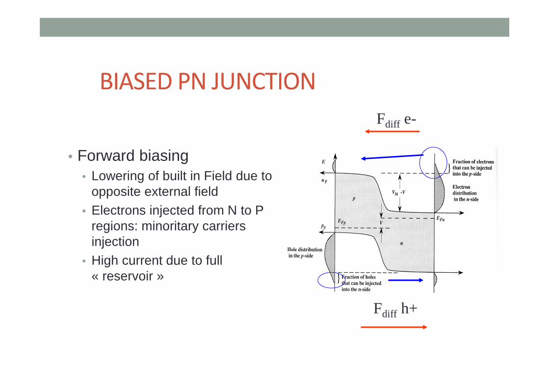
• Forward biasing• Lowering of built in Field due to
opposite external field• Electrons injected from N to P
regions: minoritary carriers injection
• High current due to full « reservoir »
11
Fdiff e-
Fdiff h+
BIASED PN JUNCTION

Forward Biasing
12
Eext
Jonction PN sous polarisation
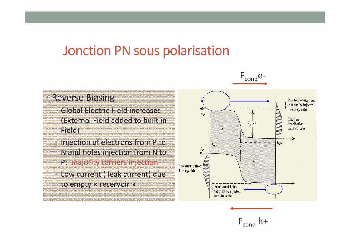
• Reverse Biasing• Global Electric Field increases(External Field added to built in Field)
• Injection of electrons from P to N and holes injection from N to P: majority carriers injection
• Low current ( leak current) due to empty « reservoir »
• Reverse Biasing• Global Electric Field increases(External Field added to built in Field)
• Injection of electrons from P to N and holes injection from N to P: majority carriers injection
• Low current ( leak current) due to empty « reservoir »
13
Fconde‐
Fcond h+
PN Junction under biasing
14
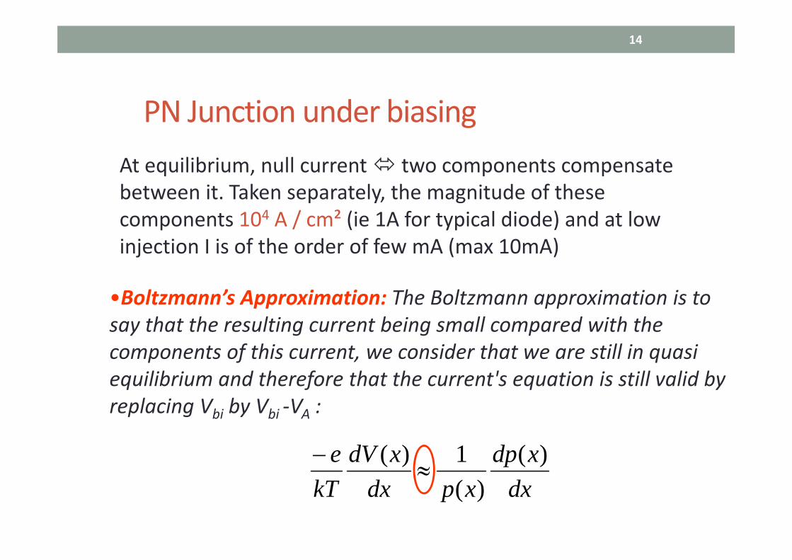
•Boltzmann’s Approximation: The Boltzmann approximation is to say that the resulting current being small compared with the components of this current, we consider that we are still in quasi equilibrium and therefore that the current's equation is still valid by replacing Vbi by Vbi ‐VA :
At equilibrium, null current two components compensatebetween it. Taken separately, the magnitude of these components 104 A / cm² (ie 1A for typical diode) and at low injection I is of the order of few mA (max 10mA)
dxxdp
xpdxxdV
kTe )(
)(1)(

Density of carriers injected to the limits of depletionlayer
• If Va=0
• If Va
15
)exp()(kTeV
pp
pWp bi
p
n
p
N
0 )exp())(exp(')('kTeV
pp
kTVVe
pp
pWp A
p
nAbi
p
n
p
N
)exp()exp('2
kTeV
Nn
kTeV
pp A
D
iAnn )exp()exp('
2
kTeV
Nn
kTeVnn A
A
iApp
)exp(** 2''
kTeVnnppn a
innpp

Holes density injected versus bias voltage Va
0,0 0,1 0,2 0,3 0,4 0,5 0,6 0,7104
105
106
107
108
109
1010
1011
1012
1013
1014
1015
1016
1017
Na= 1E17 cm-3
Vd=0.7 V
P'(W
n) (c
m-3)
Va (V) 16

Minority carriers distribution in neutral region
• Due to gradient concentration, carriers will diffuse and produce diffusion current (no electric field in neutral region!)
• Distribution is geometrydependant
• Discrimatory parameter : length diffusion LDn,p of electrons and holes and neutral region widths dn,p
17
-WP 0 WN

Minority carriers distribution in neutral region
• Long regions ( )
18
nppn Ld ,,
pNa
LxWkTeV
nn eeppxp /)()1()(' pNa
LxWkTeV
nn eeppxp /)()1()('
n
aLWpxkT
eV
pp eennxn /)()1()(' n
aLWpxkT
eV
pp eennxn /)()1()('
Short (narrow) regions ( )nppn Ld ,,
))(1()(' xxedp
pxp ckTeV
n
nn
a
))(1()(' xxedp
pxp ckTeV
n
nn
a
)')(1()(' xxedn
nxn ckTeV
p
pp
a
)')(1()(' xxedn
nxn ckTeV
p
pp
a
General case
p
ckTeV
p
n
nn L
xxshe
Ld
sh
ppxp
a
)1()(
)('
n
ckTeV
n
p
pp L
xxshe
Ld
sh
nnxn
a '
)1()(
)('
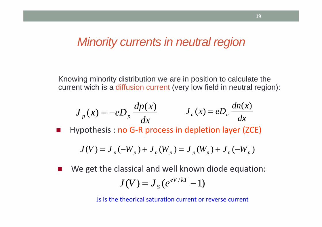
Minority currents in neutral region
Knowing minority distribution we are in position to calculate the current wich is a diffusion current (very low field in neutral region):
19
dxxdpeDxJ pp)()( dx
xdneDxJ nn)()(
Hypothesis : no G‐R process in depletion layer (ZCE)
)()()()()( pnnppnpp WJWJWJWJVJ
We get the classical and well known diode equation:
)1()( / kTeVS eJVJ
Js is the theorical saturation current or reverse current

20
-WP 0 WN
pA
ni
nD
PiS dN
DendNDen
J22
Long region
nA
ni
PD
PiS LN
DenLNDen
J22
General case
)()(
22
n
pnA
ni
P
nPD
PiS
Ld
thLN
Den
Ld
thLN
DenJ
Minority currents in neutral region
Short (Narrow) region
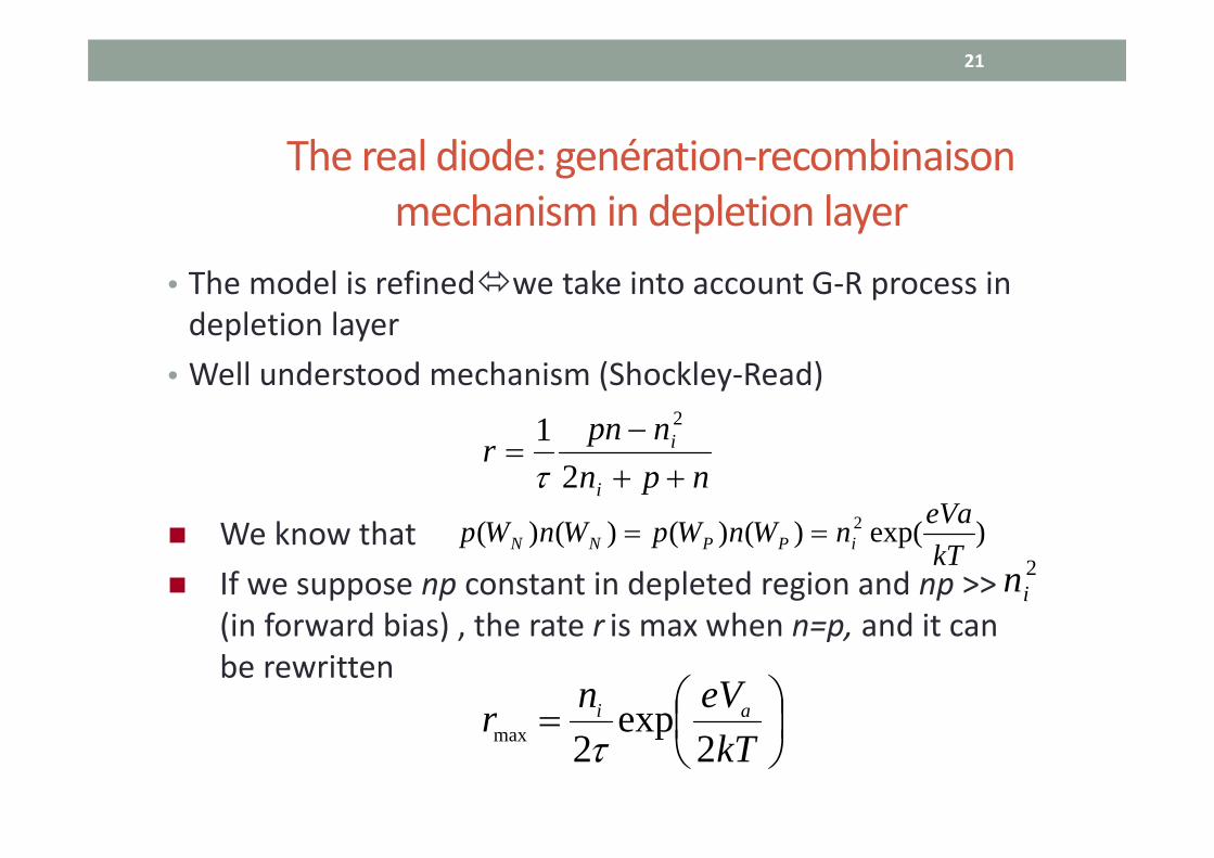
• The model is refinedwe take into account G‐R process in depletion layer
• Well understood mechanism (Shockley‐Read)
The real diode: genération‐recombinaison mechanism in depletion layer
21
npnnpn
ri
i
2
1 2
We know that If we suppose np constant in depleted region and np >>
(in forward bias) , the rate r is max when n=p, and it canbe rewritten
)exp()()()()( 2
kTeVanWnWpWnWp iPPNN
2in
kTeVnr ai
2exp
2max
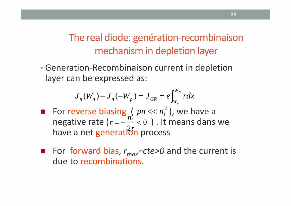
• Generation‐Recombinaison current in depletionlayer can be expressed as:
22
N
P
W
WGRpnnn rdxeJWJWJ )()(
For reverse biasing ( ), we have a negative rate ( ) . It means dans wehave a net generation process
2inpn
02
in
r
For forward bias, rmax=cte>0 and the current isdue to recombinations.
The real diode: genération‐recombinaison mechanism in depletion layer
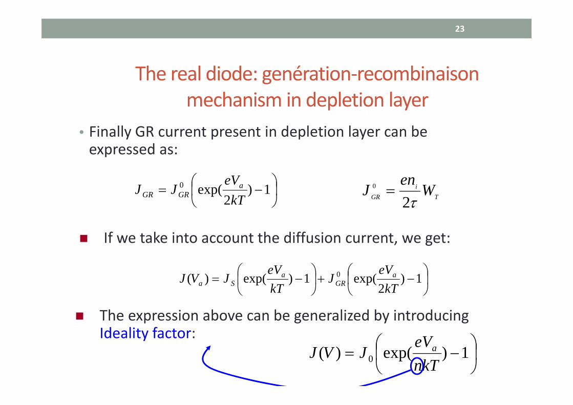
• Finally GR current present in depletion layer can beexpressed as:
23
If we take into account the diffusion current, we get:
1)
2exp(0
kTeV
JJ aGRGR
1)
2exp(1)exp()( 0
kTeV
JkTeV
JVJ aGR
aSa
Ti
GR Wen
J2
0
The expression above can be generalized by introducingIdeality factor:
1)exp()( 0 nkT
eVJVJ a
The real diode: genération‐recombinaison mechanism in depletion layer
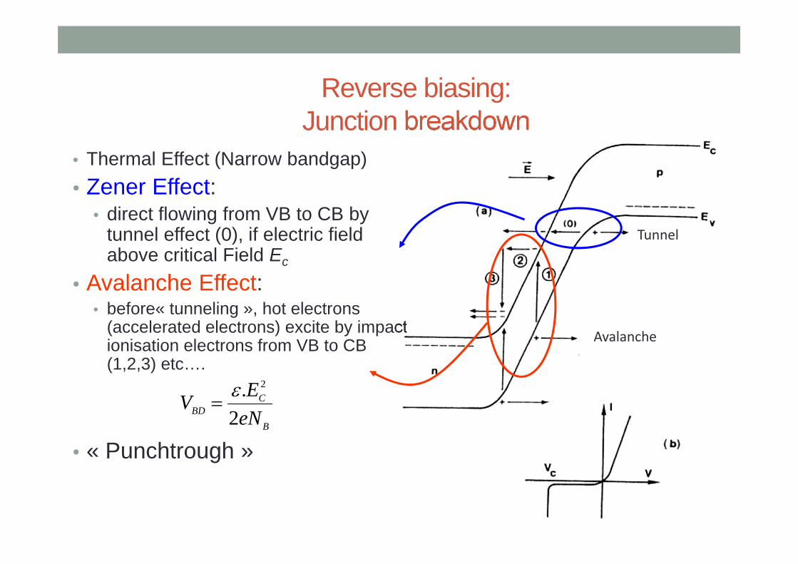
Reverse biasing: Junction breakdown
• Thermal Effect (Narrow bandgap)• Zener Effect:
• direct flowing from VB to CB by tunnel effect (0), if electric fieldabove critical Field Ec
• Avalanche Effect:• before« tunneling », hot electrons
(accelerated electrons) excite by impact ionisation electrons from VB to CB (1,2,3) etc….
• « Punchtrough »
24
B
CBD eN
EV2
. 2
tunnelTunnel
Avalanche

Small signal model of the diode: capacitances
• Capacitance associated to charges• 2 types of charges present in the junction
• Fixed charges (ionised dopants) in depletion layer• Mobiles (e- et h+) injected when forward biasing
• 2 types of capacitance• Junction (or Transition) Capacitance • Charge Storage (or diffusion) Capacitance
25

Junction capacitance
26
Simply associated to charges present in depletion layer
dVdQCC jT NDPA WeANWeANQ
TDA
DA
ADjT W
ANN
NNVV
eACC
)()(2
2
or:
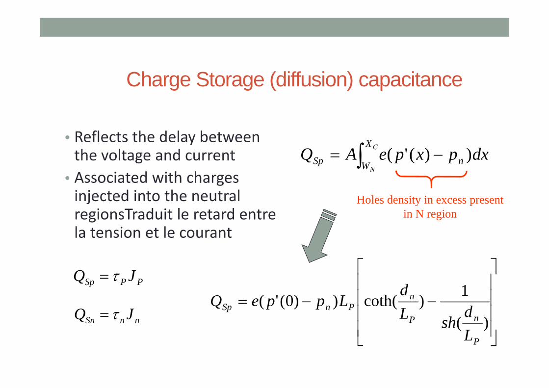
Charge Storage (diffusion) capacitance
• Reflects the delay between the voltage and current
• Associated with charges injected into the neutral regionsTraduit le retard entre la tension et le courant
27
PPSp JQ
nnSn JQ
C
N
X
W nSp dxpxpeAQ ))('(
Holes density in excess presentin N region
)(
1)coth())0('(
P
nP
nPnSp
Ld
shLd
LppeQ

28
Charge Storage (diffusion) capacitance
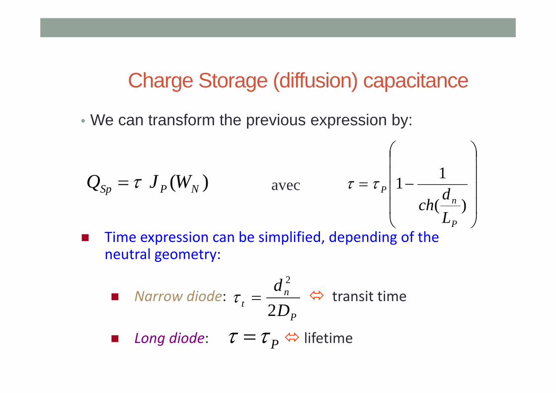
• We can transform the previous expression by:
29
)( NPSp WJQ avec
)(
11
P
nP
Ld
ch
Time expression can be simplified, depending of the neutral geometry:
Narrow diode: transit time
Long diode: lifetimeP
nt D
d2
2
P
Charge Storage (diffusion) capacitance
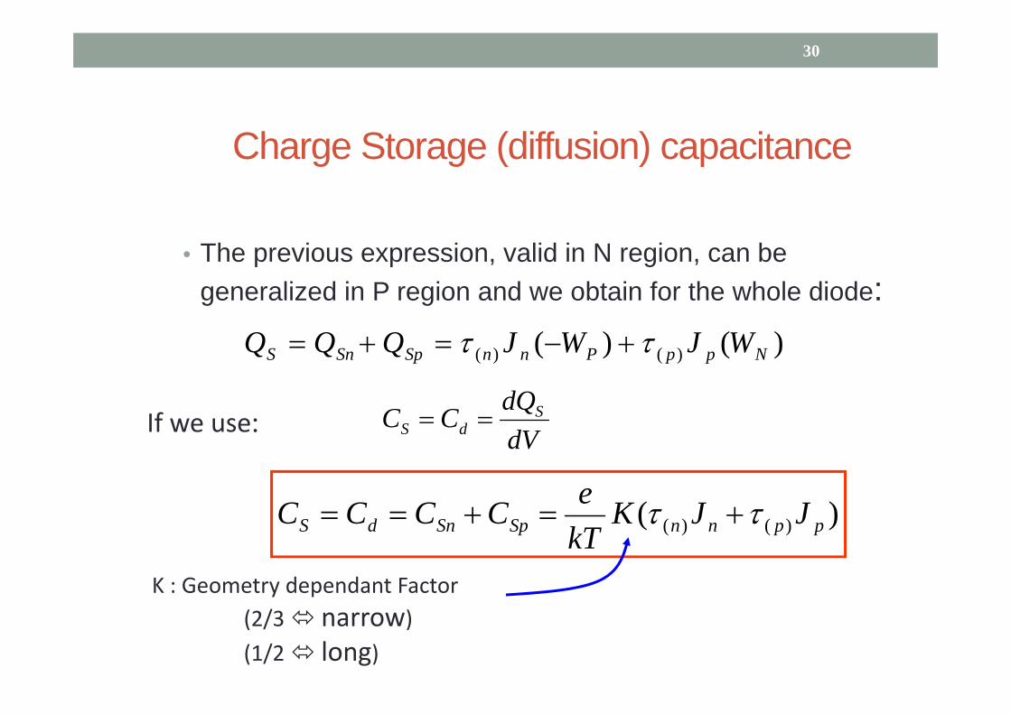
• The previous expression, valid in N region, can begeneralized in P region and we obtain for the whole diode:
30
)()( )()( NppPnnSpSnS WJWJQQQ
If we use: dVdQCC S
dS
)( )()( ppnnSpSndS JJKkTeCCCC
K : Geometry dependant Factor (2/3 narrow)(1/2 long)
Charge Storage (diffusion) capacitance

Equivalent circuit of foward diode
31
rd : diode resistance (dynamic resistance) given by the differential slope of the I‐V characteristics
rs : serie resistance of neutral region n and pIe
kTrd1
(from Neamen)

Large signal switching of diode
32
As long as the stored charge is positive forward bias diode voltage acrossdiode is small (few 10 mV)
)1(' kTeV
nnn
a
eppp
sd Storage time ie nN pWp )('
Wn

• Storage time :The main problem in minoritary carriers devices:• Storage time:
• Rise (or fall) time :
• Cj: mean value of capacitance between zero and –V2
33
)1ln()1ln(
mf
f
m
fpsd II
III
mf
fjFf II
IRC
avec 1
3.2
Large signal switching of diode
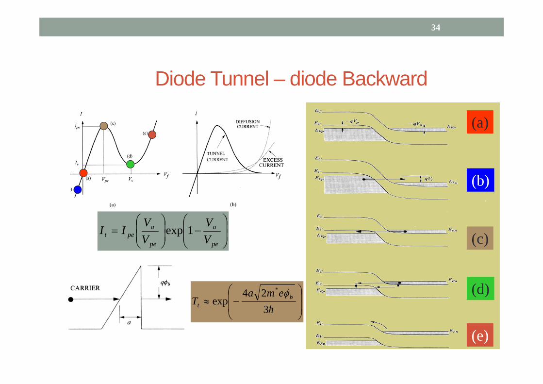
Diode Tunnel – diode Backward
34
324
exp*
bt
emaT
pe
a
pe
apet V
VVV
II 1exp
(a)
(e)
(d)
(c)
(b)
Related Documents