Pixel Crosstalk and Correlation with Modulation Transfer Function of CMOS Image Sensor M.Estribeau*, P.Magnan** SUPAERO – Integrated Image Sensors Laboratory 10 avenue Edouard Belin, 31400 Toulouse, France ABSTRACT The Modulation Transfer Function is a common metric used to quantify image quality but inter-pixel crosstalk analysis is also of interest. Because of an important number of parameters influencing MTF, its analytical calculation and crosstalk predetermination are not an easy task for a CMOS image sensor. A dedicated test chip (using a technology optimized for imaging applications) has been developed in order to get both MTF data and influence of the various areas of the pixel to its own response and the one of its neighbors. In order to evaluate the contribution of pixel elementary patterns (particularly the in-pixel readout circuitry), several kernels of shielded pixels have been implemented with the central pixel locally unmasked. The results obtained with pixel kernels and direct MTF measurements, performed on the same chip at different wavelengths, are analyzed and compared in order to correlate them and draw conclusions that can be applied at the design level. Additional data resulting from spotscan measurements allow us to verify our hypothesis on different pixels. Keywords : CMOS Image Sensors, Crosstalk, Modulation Transfer Function. 1. INTRODUCTION Crosstalk in an image sensor results from photo-generated carriers having the possibility to diffuse and to be collected by a neighboring pixel. It occurs in both monochrome and color image sensors. In this last case, crosstalk makes poor color separation and its reduction may avoid color mixing. Our study concerns monochrome CMOS Image Sensors. We have developed a 1Kx1K-photodiode pixels array for space applications. The pixel size – 13μm pitch – may be considered as medium. For sensing and pointing applications, an important crosstalk may affect centroiding determination accuracy. For imaging applications, it yields to a loss of resolution, i.e. a poor image quality, commonly quantified by the Modulation Transfer Function (MTF). So, crosstalk study is of primary importance for our applications. In the case of an image sensor, the MTF is a combination of different MTFs, each degrading the overall performance of the device. The main components are the integration and the diffusion MTFs. The first one takes into account the influence of the pixel size (giving the spatial sampling frequency) but also the photosensitive area size and shape (figure 1). The diffusion MTF describes the image degradation due to crosstalk between adjacent pixels. So it is depending on wavelength and doping profile of the photo-element (figure 2). * [email protected]; phone +33 5 62 17 82 51; fax +33 5 62 17 83 45 ** [email protected]; phone +33 5 62 17 80 79; fax +33 5 62 17 83 45

Welcome message from author
This document is posted to help you gain knowledge. Please leave a comment to let me know what you think about it! Share it to your friends and learn new things together.
Transcript

Pixel Crosstalk and Correlation with Modulation Transfer Function of CMOS Image Sensor
M.Estribeau*, P.Magnan**
SUPAERO – Integrated Image Sensors Laboratory 10 avenue Edouard Belin, 31400 Toulouse, France
ABSTRACT The Modulation Transfer Function is a common metric used to quantify image quality but inter-pixel crosstalk analysis is also of interest. Because of an important number of parameters influencing MTF, its analytical calculation and crosstalk predetermination are not an easy task for a CMOS image sensor. A dedicated test chip (using a technology optimized for imaging applications) has been developed in order to get both MTF data and influence of the various areas of the pixel to its own response and the one of its neighbors. In order to evaluate the contribution of pixel elementary patterns (particularly the in-pixel readout circuitry), several kernels of shielded pixels have been implemented with the central pixel locally unmasked. The results obtained with pixel kernels and direct MTF measurements, performed on the same chip at different wavelengths, are analyzed and compared in order to correlate them and draw conclusions that can be applied at the design level. Additional data resulting from spotscan measurements allow us to verify our hypothesis on different pixels.
Keywords : CMOS Image Sensors, Crosstalk, Modulation Transfer Function.
1. INTRODUCTION
Crosstalk in an image sensor results from photo-generated carriers having the possibility to diffuse and to be collected by a neighboring pixel. It occurs in both monochrome and color image sensors. In this last case, crosstalk makes poor color separation and its reduction may avoid color mixing.
Our study concerns monochrome CMOS Image Sensors. We have developed a 1Kx1K-photodiode pixels array for space applications. The pixel size – 13µm pitch – may be considered as medium. For sensing and pointing applications, an important crosstalk may affect centroiding determination accuracy. For imaging applications, it yields to a loss of resolution, i.e. a poor image quality, commonly quantified by the Modulation Transfer Function (MTF). So, crosstalk study is of primary importance for our applications.
In the case of an image sensor, the MTF is a combination of different MTFs, each degrading the overall performance of the device. The main components are the integration and the diffusion MTFs. The first one takes into account the influence of the pixel size (giving the spatial sampling frequency) but also the photosensitive area size and shape (figure 1). The diffusion MTF describes the image degradation due to crosstalk between adjacent pixels. So it is depending on wavelength and doping profile of the photo-element (figure 2).
* [email protected]; phone +33 5 62 17 82 51; fax +33 5 62 17 83 45 ** [email protected]; phone +33 5 62 17 80 79; fax +33 5 62 17 83 45
mersadier
Zone de texte
Copyright 2005 Society of Photo-Optical Instrumentation Engineers. This paper was published in "Proceedings of SPIE - Volume 5677 - Sensors and Camera Systems for Scientific and Industrial Applications VI" and is made available as an electronic reprint with permission of SPIE. One print or electronic copy may be made for personal use only. Systematic or multiple reproduction, distribution to multiple locations via electronic or other means, duplication of any material in this paper for a fee or for commercial purposes, or modification of the content of the paper are prohibited.
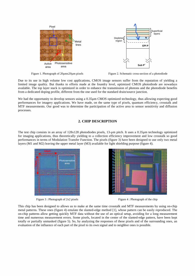
Photosensitive
area Active area
Pixel
Metal lines
Depletedregion
EPI P
Sub P+
N
Superficiallayers
Figure 1. Photograph of 20µmx20µm pixels Figure 2. Schematic cross-section of a photodiode
Due to its use in high volume low cost applications, CMOS image sensors suffer from the reputation of yielding a limited image quality. But thanks to efforts made at the foundry level, optimized CMOS photodiode are nowadays available. The top layer stack is optimized in order to enhance the transmission of photons and the photodiode benefits from a dedicated doping profile, different from the one used for the standard drain/source junction.
We had the opportunity to develop sensors using a 0.35µm CMOS optimized technology, thus allowing expecting good performances for imagery applications. We have made, on the same type of pixels, quantum efficiency, crosstalk and MTF measurements. Our good was to determine the participation of the active area to sensor sensitivity and diffusion processes.
2. CHIP DESCRIPTION
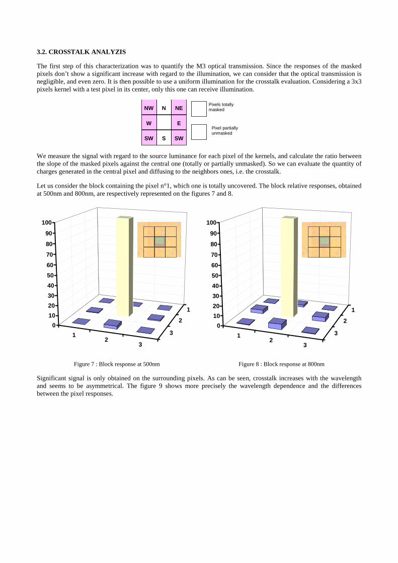
The test chip consists in an array of 128x128 photodiodes pixels, 13-µm pitch. It uses a 0.35µm technology optimized for imaging applications, thus theoretically yielding to a collection efficiency improvement and low crosstalk so good performances in terms of Modulation Transfer Function. The pixels (figure 3) have been designed to use only two metal layers (M1 and M2) leaving the upper metal layer (M3) available for light shielding purpose (figure 4).
Photosensitivearea
13µm
13µm
Figure 3 : Photograph of 2x2 pixels Figure 4 : Photograph of the chip
This chip has been designed to allows us to make at the same time crosstalk and MTF measurements by using on-chip metal patterns. These ones (figure 4) emulate the slanted-edge method [1], whose pattern can be easily reproduced. The on-chip patterns allow getting quickly MTF data without the use of an optical setup, avoiding for a long measurement time and numerous measurement errors. Some pixels, located in the center of the slanted-edge pattern, have been kept totally or partially unmasked (figure 5). So, by analyzing the responses of these pixels and of the surrounding ones, an evaluation of the influence of each part of the pixel to its own signal and to neighbor ones is possible.

12 3
54 6
89 7
10 12
13
11
Figure 5 : Photograph of the test pixels
Metal-covered pixels may have a conversion gain (CVF) different of the one of non-covered pixels (pixel capacitance is modified by the metal layer). If changes in CVF are significant, the numerical response of each pixel must be corrected of its own CVF. The detector has been entirely characterized in term of CVF before any other measurement. In our case, differences between measured CVF values are negligible due to the use of a metal layer sufficiently high.
3. ELECTRO-OPTICAL MEASUREMENTS
3.1. QUANTUM EFFICIENCY
Measurements of quantum efficiency on unmasked pixels have been made using a monochromator. Thus allows us to explore the spectral range 400-900mn with a 10 nm step. Results are shown on the figure 6.
0
10
20
30
40
50
60
400 450 500 550 600 650 700 750 800 850 900
Wavelength (nm)
QE
x F
F (
%) 51% peak (@ 560nm)
Figure 6: QE x FF for 13µm pitch pixels – 0.35µm CMOS optimized technology – 60% fill factor
As expecting, quantum efficiency results are good. Peak quantum efficiency is obtained at the wavelength of 560nm (QE x FF = 51%). The sensor also demonstrates good response in blue and red, thus proving really good performance in photon transmission and collection efficiency.
3.2. CROSSTALK ANALYZIS
The first step of this characterization was to quantify the M3 optical transmission. Since the responses of the masked pixels don’t show a significant increase with regard to the illumination, we can consider that the optical transmission is negligible, and even zero. It is then possible to use a uniform illumination for the crosstalk evaluation. Considering a 3x3 pixels kernel with a test pixel in its center, only this one can receive illumination.
Pixels totallymasked
Pixel partiallyunmasked
N
SSW
W
NW NE
E
SW
We measure the signal with regard to the source luminance for each pixel of the kernels, and calculate the ratio between the slope of the masked pixels against the central one (totally or partially unmasked). So we can evaluate the quantity of charges generated in the central pixel and diffusing to the neighbors ones, i.e. the crosstalk.
Let us consider the block containing the pixel n°1, which one is totally uncovered. The block relative responses, obtained at 500nm and 800nm, are respectively represented on the figures 7 and 8.
12
3
3
2
1
0
10
20
30
40
50
60
70
80
90
100
12
3
3
2
1
0
10
20
30
40
50
60
70
80
90
100
Figure 7 : Block response at 500nm Figure 8 : Block response at 800nm
Significant signal is only obtained on the surrounding pixels. As can be seen, crosstalk increases with the wavelength and seems to be asymmetrical. The figure 9 shows more precisely the wavelength dependence and the differences between the pixel responses.

0
1
2
3
4
5
6
7
500 550 600 650 700 750 800
Wavelength (nm)
Cro
ssta
lk (
%)
NW N NE
EW
SW S SE
Pixel 1
Figure 9 : Crosstalk evaluation on the pixel block in which the central pixel is totally unmasked
We can notice that the values measured on the W-pixel and the E-pixel are very close and that crosstalk varies quasi linearly with wavelength. Even at long wavelength, for which diffusion is very important, crosstalk values are low, thus proving the good performances of this technology for imaging applications. Regarding the curves obtained for the N-pixel and the S-pixel, crosstalk appears clearly as being asymmetric.
Similar quasi-linear trends have already been found by simulation and measurements on CCD test structures [2] as on CMOS pixels [3] by photocurrent calculations. This last work showed also evident differences between crosstalk values depending on the diffusion direction. Measurements made on four CMOS image sensors (including two commercial sensors) revealed an equivalent asymmetry [4].
So, it is now interesting to wonder why, while the diffusion is isotropic, the crosstalk doesn’t show a symmetry.
3.3. ACTIVE AREA PARTICIPATION TO CROSSTALK AND QE
In order to quantify the participation of the entire active area to the crosstalk, we study the block containing the pixel n°2 (active area totally covered by the upper metal layer). Figure 10 shows the responses of the pixels surrounding the pixel n°2.
0
1
2
3
4
5
6
7
500 550 600 650 700 750 800
Wavelength (nm)
Cro
ssta
lk (
%)
Pixel 2
NW N NE
EW
SW S SE
Figure 10 : Crosstalk evaluation on the pixel block in which the central pixel active area is totally masked

While the crosstalk values are unchanged in the horizontal direction (W-pixel and E-pixel), active area masking reduces crosstalk calculated on the S-pixel. More, values obtained for the S-pixel and the N-pixel are the same so crosstalk is now symmetric.
Masking the pixels active area seems to be a great solution for crosstalk reduction. However, effects on quantum efficiency must be verified. The figure 11 shows quantum efficiency measured for pixel n°1 and n°2.
0
10
20
30
40
50
60
400 450 500 550 600 650 700 750 800 850 900
Wavelength (nm)
QE
x F
F (
%)
Pixel 1
Pixel 2
Figure 11: Active area masking influence on quantum efficiency
We remind that pixel n°1 is totally unmasked while the upper metal layer covers the active area of the pixel n°2. As can be seen, this induces a slight difference in quantum efficiency values – peak quantum efficiency is about 47.7% at 560nm for pixel n°2. So, we can deduce that carriers are generated in the active area, diffuse to the depletion region and participate to the pixel response.
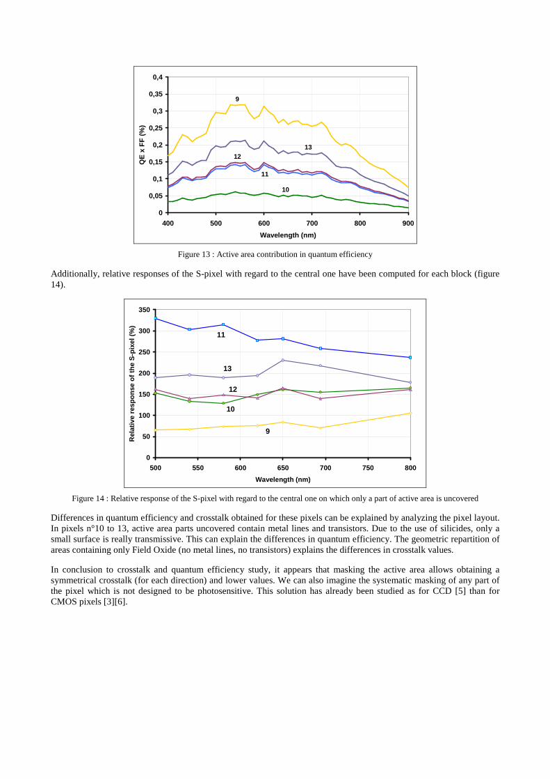
The study of pixels n°9 to n°13 would allow us to get a better knowledge of active area participation to quantum efficiency and to crosstalk. In these pixels, only a part of the active area remains uncovered (figure 12).
Uncovered pixel Pixel n°9 Pixel n°10 Pixel n°11 Pixel n°12 Pixel n°13
Figure 12 : Photograph of pixels n°9 to n°13 on which only a part of the active area is uncovered
Parts of active area remaining uncovered are about 7 µm² for each pixel. The contribution to the overall photo-response of each part of the active area can be compared by examining the relative quantum efficiency of these small windows. Results shown in figure 13 demonstrate a very non-identical contribution.
0
0,05
0,1
0,15
0,2
0,25
0,3
0,35
0,4
400 500 600 700 800 900
Wavelength (nm)
QE
x F
F (
%)
9
13
10
12
11
Figure 13 : Active area contribution in quantum efficiency
Additionally, relative responses of the S-pixel with regard to the central one have been computed for each block (figure 14).
0
50
100
150
200
250
300
350
500 550 600 650 700 750 800
Wavelength (nm)
Rel
ativ
e re
spon
se o
f the
S-p
ixel
(%
)
9
10
12
13
11
Figure 14 : Relative response of the S-pixel with regard to the central one on which only a part of active area is uncovered
Differences in quantum efficiency and crosstalk obtained for these pixels can be explained by analyzing the pixel layout. In pixels n°10 to 13, active area parts uncovered contain metal lines and transistors. Due to the use of silicides, only a small surface is really transmissive. This can explain the differences in quantum efficiency. The geometric repartition of areas containing only Field Oxide (no metal lines, no transistors) explains the differences in crosstalk values.
In conclusion to crosstalk and quantum efficiency study, it appears that masking the active area allows obtaining a symmetrical crosstalk (for each direction) and lower values. We can also imagine the systematic masking of any part of the pixel which is not designed to be photosensitive. This solution has already been studied as for CCD [5] than for CMOS pixels [3][6].

3.4. MODULATION TRANSFER FUNCTION AND SPOTSCAN MEASUREMENTS
Modulation Transfer Function measurements have been made using the slanted-edge pattern implemented at the chip level. Results have been validated by sine target and slanted-edge target measurements [7].
Figures 15 and 16 show the MTF in the horizontal and the vertical direction, measured for four wavelengths between 500nm and 800nm. The integration MTFs, calculated applying a two-dimensional Fast Fourier Transform to the photosensitive area shape [8], are also shown.
0
0,1
0,2
0,3
0,4
0,5
0,6
0,7
0,8
0,9
1
0 20 40 60 80 100 120 140
Spatial Frequency (lp/mm)
MT
F
500 nm
580 nm
650 nm
800 nm
Integration MTF
Nyquist Frequency
Sampling Frequency
0
0,1
0,2
0,3
0,4
0,5
0,6
0,7
0,8
0,9
1
0 20 40 60 80 100 120 140
Spatial Frequency (lp/mm)M
TF
500 nm
580 nm
650 nm
800 nm
Integration MTF
Nyquist Frequency
Sampling Frequency
Figure 15 : MTF in the horizontal direction (X) Figure 16 : MTF in the vertical direction (Y)
The photosensitive area has a rectangular shape, it is larger in the horizontal direction than in the vertical one. So, the vertical MTF must theoretically be better than the horizontal MTF. The following table presents values obtained at the Nyquist Frequency for the integration and the measured MTFs.
MTF X MTF Y
Integration MTF 0.70 0.79
500 nm 0.69 0.74
580 nm 0.68 0.73
650 nm 0.67 0.73
800 nm 0.63 0.68
As expecting, the vertical MTF is better than the horizontal one. We can notice that measured MTFs are very close to the integration MTF, particularly in the X direction. Higher crosstalk values obtained in the Y direction can explain the larger difference between integration and measured MTF.
Spotscan measurements allow us to confirm that the spatial photo-response contribution do match the photosensitive area shape. They have been made on these pixels with an optical spot of about 1.5µm diameter. It is obtained using a pinhole (50µm diameter) associated with a microscope objective (NA=0.55) allowing to get the Airy diffraction figure on the sensor surface. A laser source is often used for subpixel sensitivity map [9][10] but the optical setup may be complicated by the laser section diameter (about 1 mm).
The figure 17 presents measurements made in the horizontal and the vertical direction.

0
200
400
600
800
1000
0 5 10 15 20 25 30
Spot Displacement (µm)
Pix
el R
espo
nse
(AD
U)
Horizontal scan
Vertical scan
~3µm
~3µm
13µm
Figure 17 : Spotscan measurements on the 13µm pitch pixel (500nm)
The 3-µm annotated on the figure corresponds to the dimension of the active area in the Y direction. The edges sharpness allows us to confirm that the integration MTF, only taking in consideration the photosensitive area shape, is a good approximation of the sensor MTF.
3.5. STUDY OF DIFFERENT PIXELS
The MTF and spotscan measurements made on this pixel (13µm pitch – 2 metal layer) allow us to think that the photosensitive area shape is preponderant. In order to check if this is due to the technology used, we have made spotscan measurements on two other types of pixels having a different geometry. The both use three metal layer but the first one is a 13µm pitch pixel even while the second one is 10µm pitch. The wavelength of incident light being 800nm, the spot diameter is now about 2µm. The figures 18 and 19 presents the spotscan results.
0
0,1
0,2
0,3
0,4
0,5
0,6
0,7
0,8
0,9
1
0 5 10 15 20 25 30 35 40
Spot displacement (µm)
Pix
el r
espo
nse
0
0,1
0,2
0,3
0,4
0,5
0,6
0,7
0,8
0,9
1
0 5 10 15 20
Spot displacement (µm)
Pix
el r
espo
nse
Figure 18 : Spotscan measurements on the 13µm pitch – 3 metal layer pixel
Figure 19 : Spotscan measurements on the 10µm pitch – 3 metal layer pixel
In both cases, we can notice the low response of the neighbors when the spot in centered on the pixel. So, crosstalk is not of critical importance and we can expect, as with the 13µm pitch – 2 metal layer pixel, a real MTF close to the integration MTF.

3.6. CROSSTALK/MTF CORRELATION
The figure 20 represents MTF values obtained at the Nyquist frequency with regard to the crosstalk measured for the same wavelength.
0,6
0,62
0,64
0,66
0,68
0,7
0,72
0,74
0,76
0,78
0,8
0 1 2 3 4 5 6
Crosstalk (%)
MT
F
500 nm580 nm
650 nm
800 nm
800 nm
650 nm
580 nm
500 nm
Integration MTF (Y)
Integration MTF (X)
X direction
Y direction
Figure 20 : MTF @Nyquist frequency vs. crosstalk
MTF values obtained in the horizontal direction depend quasi-linearly on crosstalk measured at the same wavelength. This trend is not as much evident in the vertical direction. The crosstalk aspect observed for the S-pixel may explain this.
CONCLUSION This work allow us to bring up the active area participation to pixel response (quantum efficiency) and to crosstalk. This one varies quasi-linearly with wavelength but presents a dissymmetry mostly due to active area organization. Masking active area appears as a good solution to reduce crosstalk by recovering a symmetry and without an important loss in quantum efficiency.
Thanks to the use of an optimized technology, we can observe a quasi –linear dependence of MTF on crosstalk values, which ones are very low. In such a way, the photosensitive area shape is preponderant. So, the integration MTF, obtained applying a 2D FFT to the photosensitive area shape, allow to get a good approximation of the sensor MTF mostly if a mask is applied on the active area.
ACKOWLEDGMENTS The authors want to thank Franck Corbière and Céline Engel (Supaero Integrated Image Sensors Laboratory) respectively for their help in designing the test array and for the spotscan measurements. Thanks to EADS Astrium for its financial and technical support (especially Olivier Saint-Pé and Bertrand Calvel).

REFERENCES
1. International Standard ISO 12233:2000(E) 2. J.P.Lavine, W-C.Chang, C.N.Agnastopoulos et al., "Monte Carlo Simulation of the Photoelectron Crosstalk in
Silicon Imaging Devices", IEEE transactions on Electron Devices, Vol.32, n°10, October 1985, pp 2087-2091. 3. H.Mutoh, ,"3-D Optical and Electrical Simulation for CMOS Image Sensor", IEEE transactions on Electron
Devices, Vol.50, n°1, January 2003, pp 19-25. 4. J.S.Lee, M.E.Jernigan, R.I.Hornsey, ,"Empirical Characterization of Lateral Crosstalk for CMOS Image Sensors and
Deblurring Operations", IEEE workshop on Charge-Coupled Devices and Advanced Image Sensors, Elmau, Allemagne, 15-17 May 2003.
5. A.Toyoda, Y.Suzuki, K.Orihara, Y.Hokari, ,"A Novel Tungsten Light-Shiel Structure for High-Density CCD Image Sensors", IEEE transactions on Electron Devices, Vol.38, n°5, May 1991, pp 965-968.
6. M.Furumiya, H.Ohkubo, Y.Muramatsu et al., ,"High-Sensitivity and No-Crosstalk Pixel Technology for Embedded CMOS Image Sensor", IEEE transactions on Electron Devices, Vol.48, n°10, October 2001, pp 2221-2227.
7. M.Estribeau, P.Magnan, "Fast MTF measurement of CMOS imagers using ISO 12233 slanted-edge methodology", SPIE Optical Systems Design 2003, Proceeding of SPIE, Vol.5251, October 2003.
8. O.Yadid-Pecht, "Geometrical modulation transfer function for different pixel active area shapes", Optical Engineering,, Vol.39, n°4, April 2000, pp 859-865.
9. D.Kavaldjiev, Z.Ninkov, "Subpixel sensitivity map for a charge-coupled device sensor", Optical Engineering,, Vol.37, n°3, March 1998, pp 948-954.
10. T.Dutton, J.Kang &al., "Measurement and Analysis of Pixel Geometric and Diffusion modulation Transfer Function Components in Photodiode Active Pixel Sensors", IEEE workshop on Charge-Coupled Devices and Advanced Image Sensors, Elmau, Germany, 15-17 May 2003..
Related Documents