h Phototransistor The phototransistor is a semiconductor light sensor formed from a basic transistor with a transparent cover that provides much better sensitivity than a photodiode

Phototransistors
Jul 19, 2015
Welcome message from author
This document is posted to help you gain knowledge. Please leave a comment to let me know what you think about it! Share it to your friends and learn new things together.
Transcript
h
Phototransistor
The phototransistor is a semiconductor light sensor formed from a basic transistor with a transparent cover that provides much better sensitivity than a
photodiode

Phototransistor structure
• The photo transistor has much larger base and collector areas than would be used for a normal transistor. These devices were generally made using diffusion or ion implantation.
•
• Early photo transistors used germanium or silicon throughout the device giving a homo-junction structure. The more modern phototransistors use type III-V materials such as gallium arsenide and the like

-CONTD-
• Heterostructures that use different materials either side of the p-n junction are also popular because they provide a high conversion efficiency.
• These are generally fabricated using epitaxial growth of materials that have matching lattice structures.
• These photo transistors generally use a mesa structure.
• Sometimes a Schottky (metal semiconductor) junction can be used for the collector within a phototransistor, although this practice is less common these days because other structures offer better levels of performance.
-CONTD-
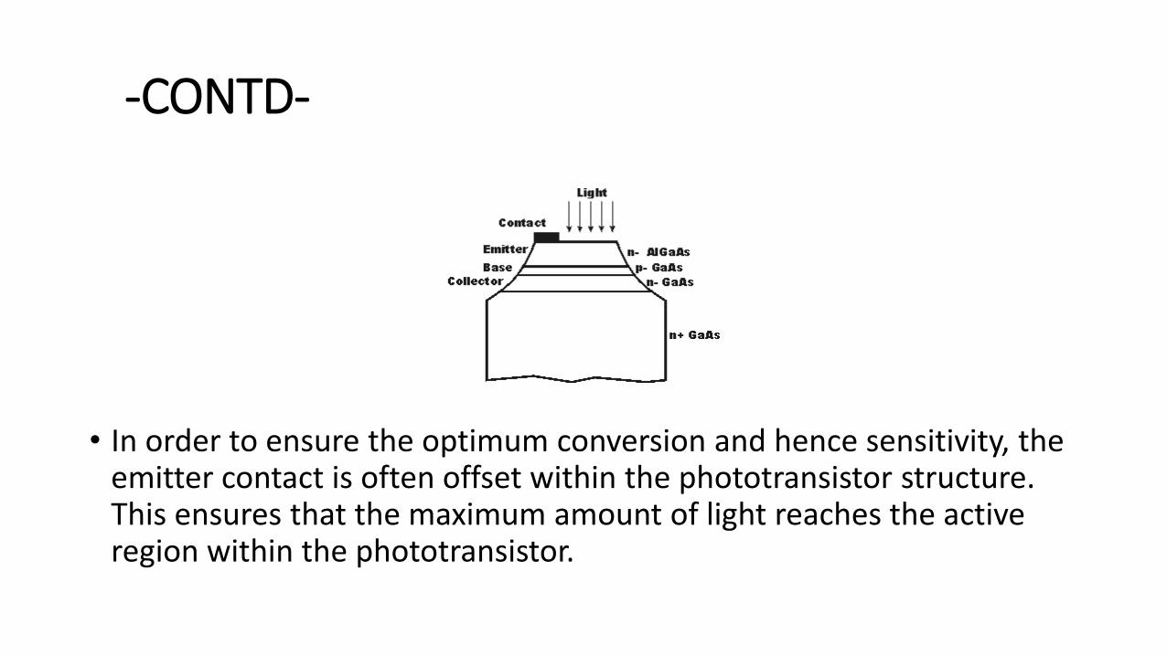
• In order to ensure the optimum conversion and hence sensitivity, the emitter contact is often offset within the phototransistor structure. This ensures that the maximum amount of light reaches the active region within the phototransistor.
Phototransistor operation
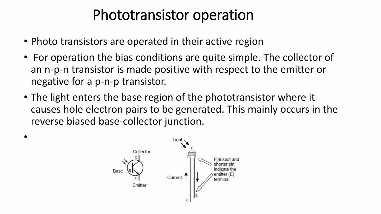
• Photo transistors are operated in their active region
• For operation the bias conditions are quite simple. The collector of an n-p-n transistor is made positive with respect to the emitter or negative for a p-n-p transistor.
• The light enters the base region of the phototransistor where it causes hole electron pairs to be generated. This mainly occurs in the reverse biased base-collector junction.
•
-CONTD-
• The hole-electron pairs move under the influence of the electric field and provide the base current, causing electrons to be injected into the emitter.
Phototransistor characteristics
• The photo transistor has a high level of gain resulting from the transistor action.
-For homo-structures, i.e. ones using the same material throughout the device, this may be of the order of about 50 up to a few hundred.
-However for the hetero-structure devices, the levels of gain may rise to ten thousand.
-Despite their high level of gain the hetero-structure devices are not widely used because they are considerably more costly to manufacture.
• The characteristics of the photo-transistor under different light intensities. They are very similar to the characteristics of a conventional bipolar transistor, but with the different levels of base current replaced by the different levels of light intensity.
-CONTD-
• There is a small amount of current that flows in the photo transistor even when no light is present. This is called the dark current, and represents the small number of carriers that are injected into the emitter.

ADVANTAGES
• A further advantage of all phototransistors when compared to the avalanche photodiode, another device that offers gain, is that the phototransistor has a much lower level of noise.
DISADVANTAGE
• One of the main disadvantages of the phototransistor is the fact that it does not have a particularly good high frequency response.
- This arises from the large capacitance associated with the base-collector junction. This junction is designed to be relatively large to enable it to pick up sufficient quantities of light.
- For a typical homo-structure device the bandwidth may be limited to about 250 kHz.
-Hetero-junction devices have a much higher limit and some can be operated at frequencies as high as 1 GHz.

Phototransistor symbol
• The phototransistor symbol for use in electronic circuit diagrams is very straightforward. It is formed from the basic transistor symbol with arrows point in to it to indicate that it is light sensitive.
• The phototransistor symbol often has two arrows pointing towards it, but other phototransistor symbols show a jagged arrow. Both versions of the phototransistor symbol are acceptable and understood.

Phototransistor circuit configurations
• The phototransistor can be used in a variety of different circuit configurations. Like more conventional transistors, the phototransistor can be used in common emitter and common collector circuits. Common base circuits are not normally used because the base connection is often left floating.
• The choice of common emitter or common collector phototransistor circuit configuration depends upon the requirements for the circuit. The two phototransistor circuit configurations have slightly different operating characteristics and these may determine the circuit used.
•

Common emitter phototransistor circuit• The common emitter phototransistor circuit configuration is possibly
the most widely used, like its more conventional straight transistor circuit. The collector is taken to the supply voltage via a collector load resistor, and the output is taken from the collector connection on the phototransistor. The circuit generates an output that moves from a high voltage state to a low voltage state when light is detected.
• The circuit actually acts as an amplifier. The current generated by the light affects the base region. This is amplified by the current gain of the transistor in the normal way.

Common collector phototransistor circuit
• The common collector, or emitter follower phototransistor circuit configuration has effectively the same topology as the normal common emitter transistor circuit - the emitter is taken to ground via a load resistor, and the output for the circuit being taken from the emitter connection of the device.
• The circuit generates an output that moves from the low state to a high state when light is detected.
Phototransistor circuit operation
• The phototransistor circuits can be used on one of two basic modes of operation. They are called active or linear mode and a switch mode.
• Operation in the "linear" or active mode provides a response that is very broadly proportional to the light stimulus. In reality the phototransistor does not give a particularly linear output to the input stimulus and it is for this reason that this mode of operation is more correctly termed the active mode.
-CONTD-
• The operation of the phototransistor circuit in the switch mode is more widely used in view of the non-linear response of the phototransistor to light. When there is little or no light, virtually no current will flow in the transistor, and it can be said to be in the "off" state. However as the level of light increases, current starts to flow. Eventually a point is reached where the phototransistor becomes saturated and the level of current cannot increase. In this situation the phototransistor is said to be saturated. The switch mode, therefore has two levels: - "on" and "off" as in a digital or logic system. This type of phototransistor mode is useful for detecting objects, sending data or reading encoders, etc.
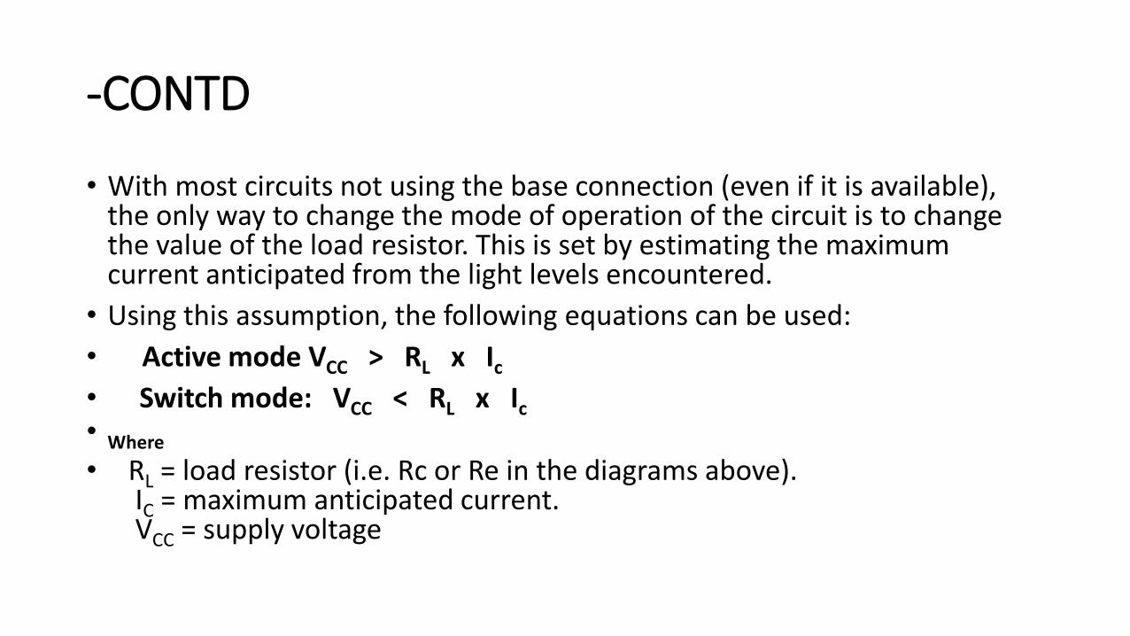
-CONTD
• With most circuits not using the base connection (even if it is available), the only way to change the mode of operation of the circuit is to change the value of the load resistor. This is set by estimating the maximum current anticipated from the light levels encountered.
• Using this assumption, the following equations can be used:
• Active mode VCC > RL x Ic
• Switch mode: VCC < RL x Ic
• Where
• RL = load resistor (i.e. Rc or Re in the diagrams above).IC = maximum anticipated current.VCC = supply voltage
Related Documents