Ultrasensitive and fast monolayer WS 2 phototransistors realized by SnS nanosheet decoration Zhiyan Jia 1 , Songlin Li 2 , Jianyong Xiang 1* , Fusheng Wen 1* , Xuan Bao 1 , Shanghuai Feng 1 , Ruilong Yang 1 , Zhongyuan Liu 1* 1 State Key Laboratory of Metastable Materials Science and Technology, Yanshan University, Qinghuangdao 066004, China. 2 School of Electronic Science and Engineering, Nanjing University, Nanjing 210093, China Keywords: Photoresponsivity, monolayer WS 2 , SnS nanosheet, chemical vapour deposition, liquid-phase exfoliation *Corresponding authors. Email: [email protected] (J. Y. Xiang), [email protected] (F. S. Wen), [email protected] (Z. Y. Liu) Electronic Supplementary Material (ESI) for Nanoscale. This journal is © The Royal Society of Chemistry 2017

Welcome message from author
This document is posted to help you gain knowledge. Please leave a comment to let me know what you think about it! Share it to your friends and learn new things together.
Transcript
Ultrasensitive and fast monolayer WS2 phototransistors realized by
SnS nanosheet decoration
Zhiyan Jia1, Songlin Li2, Jianyong Xiang1*, Fusheng Wen1*, Xuan Bao1, Shanghuai Feng1,
Ruilong Yang1, Zhongyuan Liu1*
1State Key Laboratory of Metastable Materials Science and Technology, Yanshan University,
Qinghuangdao 066004, China.
2School of Electronic Science and Engineering, Nanjing University, Nanjing 210093, China
Keywords: Photoresponsivity, monolayer WS2, SnS nanosheet, chemical vapour deposition,
liquid-phase exfoliation
*Corresponding authors.
Email: [email protected] (J. Y. Xiang), [email protected] (F. S. Wen), [email protected] (Z. Y. Liu)
Electronic Supplementary Material (ESI) for Nanoscale.This journal is © The Royal Society of Chemistry 2017
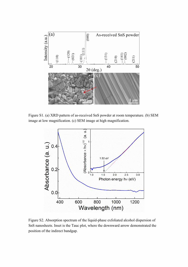
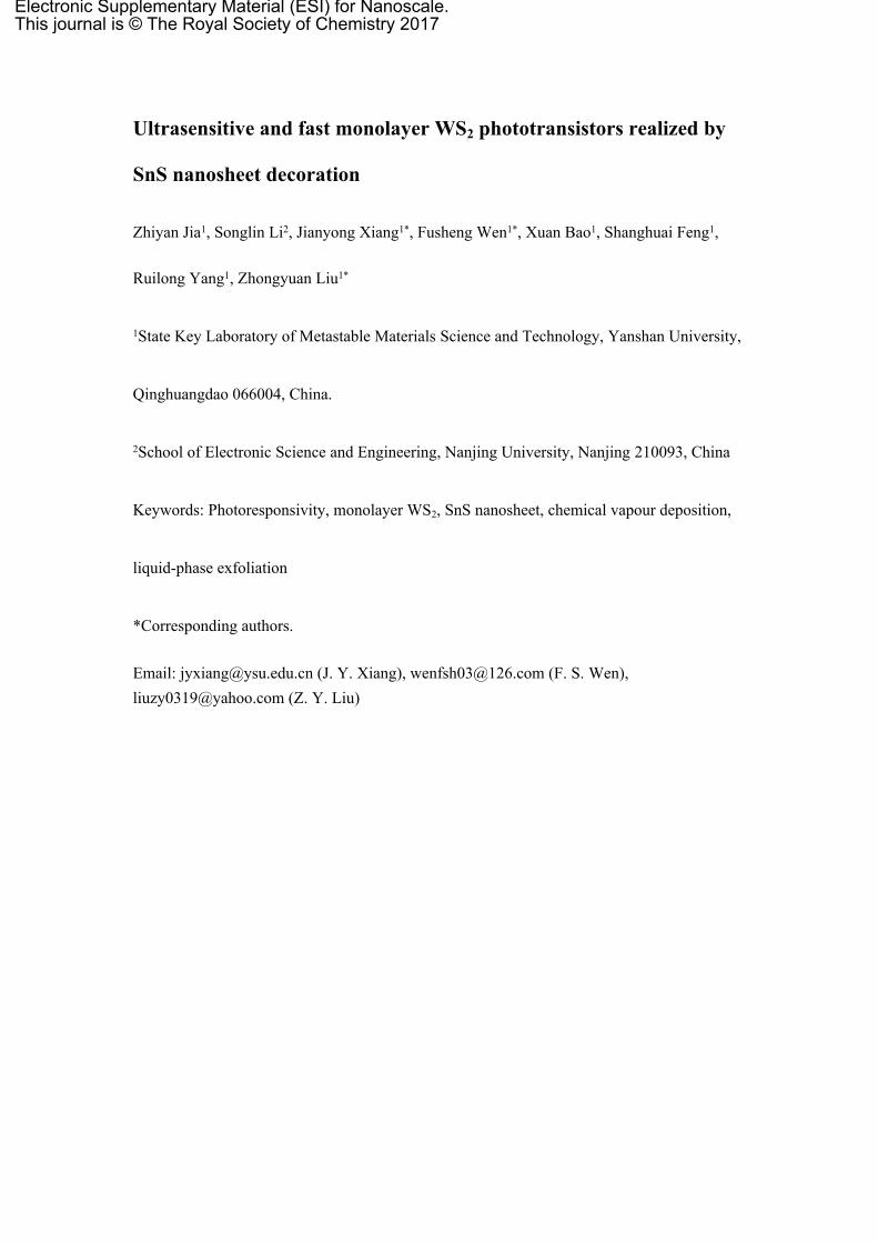
Figure S1. (a) XRD pattern of as-received SnS powder at room temperature. (b) SEM image at low magnification. (c) SEM image at high magnification.
Figure S2. Absorption spectrum of the liquid-phase exfoliated alcohol dispersion of SnS nanosheets. Inset is the Tauc plot, where the downward arrow demonstrated the position of the indirect bandgap.
Figure S3. XRD pattern of the decorated WS2 monolayer channel with SnS NSs in the decorated D8 device.
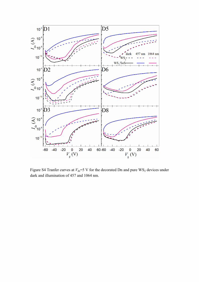
Figure S4 Tranfer curves at Vds=5 V for the decorated Dn and pure WS2 devices under dark and illumination of 457 and 1064 nm.
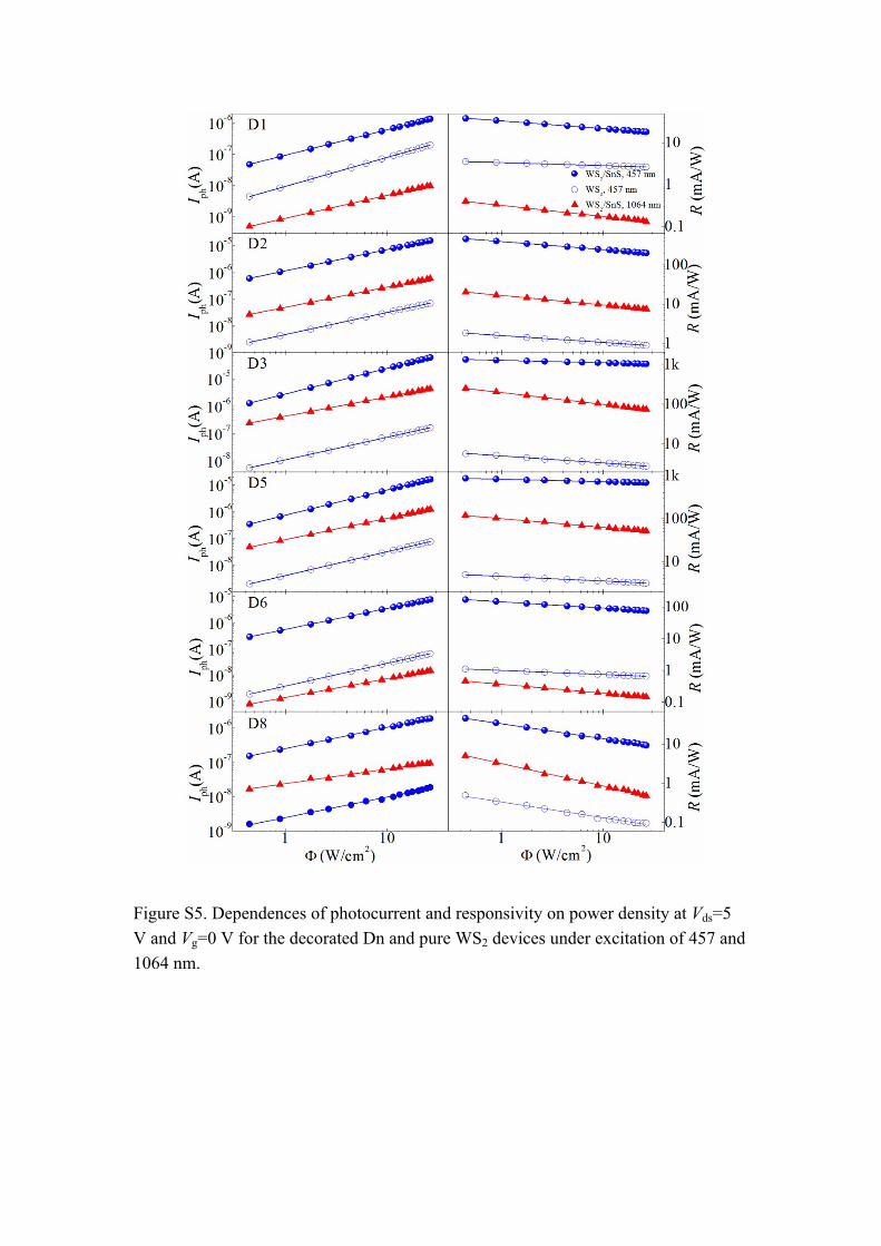
Figure S5. Dependences of photocurrent and responsivity on power density at Vds=5 V and Vg=0 V for the decorated Dn and pure WS2 devices under excitation of 457 and 1064 nm.
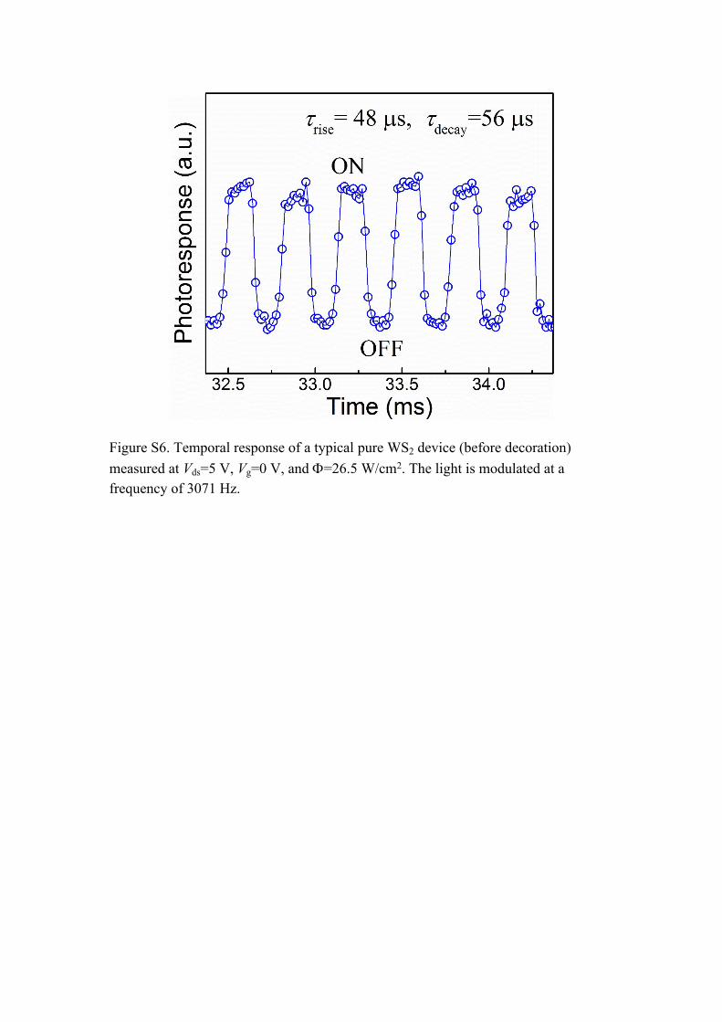
Figure S6. Temporal response of a typical pure WS2 device (before decoration) measured at Vds=5 V, Vg=0 V, and =26.5 W/cm2. The light is modulated at a frequency of 3071 Hz.
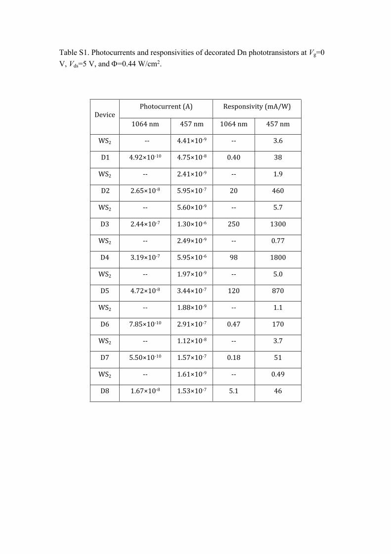
Table S1. Photocurrents and responsivities of decorated Dn phototransistors at Vg=0 V, Vds=5 V, and =0.44 W/cm2.
Photocurrent (A) Responsivity (mA/W)Device
1064 nm 457 nm 1064 nm 457 nm
WS2 -- 4.41×10⁻⁹ -- 3.6
D1 4.92×10⁻¹⁰ 4.75×10⁻⁸ 0.40 38
WS2 -- 2.41×10⁻⁹ -- 1.9
D2 2.65×10⁻⁸ 5.95×10⁻⁷ 20 460
WS2 -- 5.60×10⁻⁹ -- 5.7
D3 2.44×10⁻⁷ 1.30×10⁻⁶ 250 1300
WS2 -- 2.49×10⁻⁹ -- 0.77
D4 3.19×10⁻⁷ 5.95×10⁻⁶ 98 1800
WS2 -- 1.97×10⁻⁹ -- 5.0
D5 4.72×10⁻⁸ 3.44×10⁻⁷ 120 870
WS2 -- 1.88×10⁻⁹ -- 1.1
D6 7.85×10⁻¹⁰ 2.91×10⁻⁷ 0.47 170
WS2 -- 1.12×10⁻⁸ -- 3.7
D7 5.50×10⁻¹⁰ 1.57×10⁻⁷ 0.18 51
WS2 -- 1.61×10⁻⁹ -- 0.49
D8 1.67×10⁻⁸ 1.53×10⁻⁷ 5.1 46
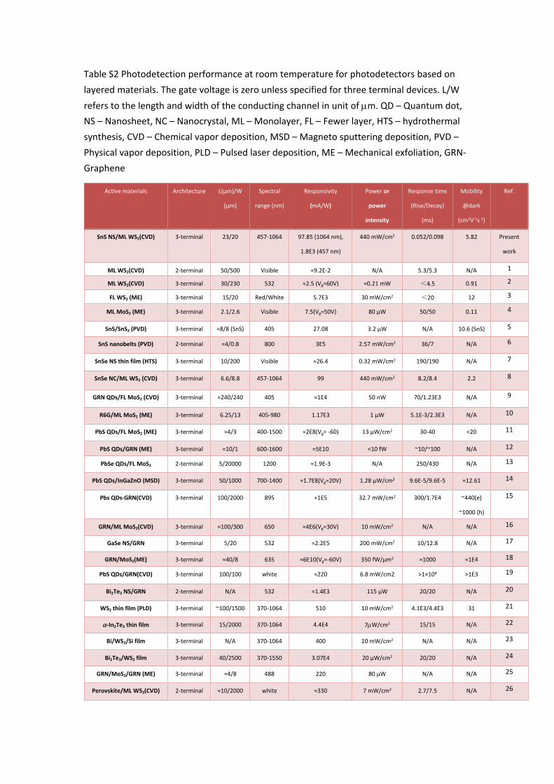
Table S2 Photodetection performance at room temperature for photodetectors based on layered materials. The gate voltage is zero unless specified for three terminal devices. L/W refers to the length and width of the conducting channel in unit of m. QD – Quantum dot, NS – Nanosheet, NC – Nanocrystal, ML – Monolayer, FL – Fewer layer, HTS – hydrothermal synthesis, CVD – Chemical vapor deposition, MSD – Magneto sputtering deposition, PVD – Physical vapor deposition, PLD – Pulsed laser deposition, ME – Mechanical exfoliation, GRN-Graphene
Active materials Architecture L(µm)/W
(μm)
Spectral
range (nm)
Responsivity
(mA/W)
Power or
power
intensity
Response time
(Rise/Decay)
(ms)
Mobility
@dark
(cm2V-1s-1)
Ref.
SnS NS/ML WS2(CVD) 3-terminal 23/20 457-1064 97.85 (1064 nm),
1.8E3 (457 nm)
440 mW/cm2 0.052/0.098 5.82 Present
work
ML WS2(CVD) 2-terminal 50/500 Visible ≈9.2E-2 N/A 5.3/5.3 N/A 1
ML WS2(CVD) 3-terminal 30/230 532 ≈2.5 (Vg=60V) ≈0.21 mW <4.5 0.91 2
FL WS2 (ME) 3-terminal 15/20 Red/White 5.7E3 30 mW/cm2 <20 12 3
ML MoS2 (ME) 3-terminal 2.1/2.6 Visible 7.5(Vg=50V) 80 μW 50/50 0.11 4
SnS/SnS2 (PVD) 3-terminal ≈8/8 (SnS) 405 27.08 3.2 μW N/A 10.6 (SnS) 5
SnS nanobelts (PVD) 2-terminal ≈4/0.8 800 3E5 2.57 mW/cm2 36/7 N/A 6
SnSe NS thin film (HTS) 3-terminal 10/200 Visible ≈26.4 0.32 mW/cm2 190/190 N/A 7
SnSe NC/ML WS2 (CVD) 3-terminal 6.6/8.8 457-1064 99 440 mW/cm2 8.2/8.4 2.2 8
GRN QDs/FL MoS2 (CVD) 3-terminal ≈240/240 405 ≈1E4 50 nW 70/1.23E3 N/A 9
R6G/ML MoS2 (ME) 3-terminal 6.25/13 405-980
nm
1.17E3 1 μW 5.1E-3/2.3E3 N/A 10
PbS QDs/FL MoS2 (ME) 3-terminal ≈4/3 400-1500
nm
≈2E8(Vg= -60) 13 μW/cm2 30-40 <20 11
PbS QDs/GRN (ME) 3-terminal ≈10/1 600-1600
nm
≈5E10 <10 fW ~10/~100 N/A 12
PbSe QDs/FL MoS2
nanoflakes
2-terminal 5/20000 1200 ≈1.9E-3 N/A 250/430 N/A 13
PbS QDs/InGaZnO (MSD) 3-terminal 50/1000 700-1400
nm
≈1.7E8(Vg=20V) 1.28 μW/cm2 9.6E-5/9.6E-5 ≈12.61 14
Pbs QDs-GRN(CVD) 3-terminal 100/2000 895 ≈1E5 32.7 mW/cm2 300/1.7E4 ~440(e)
~1000 (h)
15
GRN/ML MoS2(CVD) 3-terminal ≈100/300 650 ≈4E6(Vg=30V) 10 mW/cm2 N/A N/A 16
GaSe NS/GRN 3-terminal 5/20 532 ≈2.2E5 200 mW/cm2 10/12.8 N/A 17
GRN/MoS2(ME) 3-terminal ≈40/8 635 ≈6E10(Vg=-60V) 350 fW/μm2 ≈1000 ≈1E4 18
PbS QDs/GRN(CVD) 3-terminal 100/100 white ≈220 6.8 mW/cm2 >1×10⁴ >1E3 19
Bi2Te3 NS/GRN 2-terminal N/A 532 ≈1.4E3 115 μW 20/20 N/A 20
WS2 thin film (PLD) 3-terminal ~100/1500 370-1064
nm
510 10 mW/cm2 4.1E3/4.4E3 31 21
-In2Te3 thin film 3-terminal 15/2000 370-1064
nm
4.4E4 7W/cm2 15/15 N/A 22
Bi/WS2/Si film 3-terminal N/A 370-1064
nm
400 10 mW/cm2 N/A N/A 23
Bi2Te3/WS2 film 3-terminal 40/2500 370-1550
nm
3.07E4 20 µW/cm2 20/20 N/A 24
GRN/MoS2/GRN (ME) 3-terminal ≈4/8 488 220 80 μW N/A N/A 25
Perovskite/ML WS2(CVD) 2-terminal ≈10/2000 white ≈330 7 mW/cm2 2.7/7.5 N/A 26
References
1. N. Perea-Lopez, A. L. Elias, A. Berkdemir, A. Castro-Beltran, H. R. Gutierrez, S. M. Feng, R. T. Lv, T. Hayashi, F. Lopez-Urias, S. Ghosh, B. Muchharla, S. Talapatra, H. Terrones and M. Terrones, Adv Funct Mater, 2013, 23, 5511-5517.
2. C. Y. Lan, C. Li, Y. Yin and Y. Liu, Nanoscale, 2015, 7, 5974-5980.3. N. J. Huo, S. X. Yang, Z. M. Wei, S. S. Li, J. B. Xia and J. B. Li, Sci Rep-Uk, 2014, 4.4. Z. Y. Yin, H. Li, H. Li, L. Jiang, Y. M. Shi, Y. H. Sun, G. Lu, Q. Zhang, X. D. Chen and H.
Zhang, Acs Nano, 2012, 6, 74-80.5. J.-H. Ahn, M.-J. Lee, H. Heo, J. H. Sung, K. Kim, H. Hwang and M.-H. Jo, Nano Lett,
2015, 15, 3703-3708.6. X. Zhou, L. Gan, Q. Zhang, X. Xiong, H. Li, Z. Zhong, J. Han and T. Zhai, J Mater Chem C,
2016, 4, 2111-2116.7. L. Li, Z. Chen, Y. Hu, X. W. Wang, T. Zhang, W. Chen and Q. B. Wang, Journal of the
American Chemical Society, 2013, 135, 1213-1216.8. Z. Jia, J. Xiang, F. Wen, R. Yang, C. Hao and Z. Liu, Acs Appl Mater Inter, 2016, 8,
4781-4788.9. C. Chen, H. Qiao, S. Lin, C. Man Luk, Y. Liu, Z. Xu, J. Song, Y. Xue, D. Li, J. Yuan, W. Yu,
C. Pan, S. Ping Lau and Q. Bao, Sci Rep-Uk, 2015, 5, 11830.10. S. H. Yu, Y. Lee, S. K. Jang, J. Kang, J. Jeon, C. Lee, J. Y. Lee, H. Kim, E. Hwang, S. Lee
and J. H. Cho, Acs Nano, 2014, 8, 8285-8291.11. D. Kufer, I. Nikitskiy, T. Lasanta, G. Navickaite, F. H. L. Koppens and G. Konstantatos,
Adv Mater, 2015, 27, 176-180.12. G. Konstantatos, M. Badioli, L. Gaudreau, J. Osmond, M. Bernechea, F. P. G. de
Arquer, F. Gatti and F. H. L. Koppens, Nat Nanotechnol, 2012, 7, 363-368.13. J. Schornbaum, B. Winter, S. P. Schießl, F. Gannott, G. Katsukis, D. M. Guldi, E.
Spiecker and J. Zaumseil, Adv Funct Mater, 2014, 24, 5798-5806.14. D. K. Hwang, Y. T. Lee, H. S. Lee, Y. J. Lee, S. H. Shokouh, J.-h. Kyhm, J. Lee, H. H. Kim,
T.-H. Yoo, S. H. Nam, D. I. Son, B.-K. Ju, M.-C. Park, J. D. Song, W. K. Choi and S. Im, NPG Asia Mater, 2016, 8, e233.
15. Z. H. Sun, Z. K. Liu, J. H. Li, G. A. Tai, S. P. Lau and F. Yan, Adv Mater, 2012, 24, 5878-5883.
16. W. Zhang, C.-P. Chuu, J.-K. Huang, C.-H. Chen, M.-L. Tsai, Y.-H. Chang, C.-T. Liang, Y.-Z. Chen, Y.-L. Chueh, J.-H. He, M.-Y. Chou and L.-J. Li, Sci Rep-Uk, 2014, 4, 3826.
17. R. Lu, J. Liu, H. Luo, V. Chikan and J. Z. Wu, Sci Rep-Uk, 2016, 6, 19161.18. K. Roy, M. Padmanabhan, S. Goswami, T. P. Sai, G. Ramalingam, S. Raghavan and A.
Ghosh, Nat Nanotechnol, 2013, 8, 826-830.19. D. Zhang, L. Gan, Y. Cao, Q. Wang, L. Qi and X. Guo, Adv. Mater., 2012, 24, 2715-
2720.20. S. Li, Y. Wang, H. Qiao, J. Yuan and Q. Bao, High performance photodetectors based
on two-dimensional materials, 2015.21. J. D. Yao, Z. Q. Zheng, J. M. Shao and G. W. Yang, Nanoscale, 2015, 7, 14974-14981.22. J. Yao, Z. Deng, Z. Zheng and G. Yang, ACS Appl. Mater. Interfaces, 2016, 8, 20872-
20879.

23. J. Yao, Z. Zheng, J. Shao and G. Yang, ACS Appl. Mater. Interfaces, 2015, 7, 26701-26708.
24. J. Yao, Z. Zheng and G. Yang, J. Mater. Chem. C, 2016, 4, 7831-7840.25. W. J. Yu, Y. Liu, H. Zhou, A. Yin, Z. Li, Y. Huang and X. Duan, Nat Nano, 2013, 8, 952-
958.26. C. Ma, Y. Shi, W. Hu, M.-H. Chiu, Z. Liu, A. Bera, F. Li, H. Wang, L.-J. Li and T. Wu, Adv
Mater, 2016, 28, 3683-3689.
Related Documents