UNIVERSITY OF COPENHAGEN NIELS BOHR INSTITUTE ph.d. thesis in physics Mesoscopic Superconductivity towards Protected Qubits Author: Thorvald Wadum Larsen Supervisor: Charles M. Marcus This thesis has been submitted to the PhD School of The Faculty of Science, University of Copenhagen October 30, 2018

Welcome message from author
This document is posted to help you gain knowledge. Please leave a comment to let me know what you think about it! Share it to your friends and learn new things together.
Transcript

U N I V E R S I T Y O F C O P E N H A G E N
N I E L S B O H R I N S T I T U T E
ph.d. thesis in physics
Mesoscopic Superconductivity towards Protected Qubits
Author:
Thorvald Wadum Larsen
Supervisor:
Charles M. Marcus
This thesis has been submitted to the PhD School of
The Faculty of Science, University of Copenhagen
October 30, 2018

Abstract
This thesis presents results from experimental studies of three different approaches
towards protected qubits based on novel semiconductor nanowires proximitized by an
epitaxially grown aluminium shell.
Superconducting transmon qubits are promising candidates as building blocks in pro-
tected qubits based on quantum error correction. A Josephson junction formed in an
InAs/Al core/shell nanowire exhibit a tunable Josephson energy achieved by an elec-
trostatic gate depleting the carrier density of a semiconducting weak link region. We
integrate an InAs/Al nanowire Josephson junction into a transmonlike circuit forming a
gatemon. Embedding a gatemon into a microwave cavity we observe a vacuum-Rabi split-
ting and in the dispersive regime we measure relaxation times up to 5 µs. Additionally,
we demonstrate universal control of a two-qubit device.
Next we exploit the non-cosinusoidal energy-phase relation of high-transmission, nano-
wire Josephson junctions in a superconducting interference device to form a 0-π qubit.
The 0-π qubit can act as a fundamental building block for topologically protected qubits.
Furthermore, voltage control of the semiconductor Josephson junctions creates a unique
superconducting circuit allowing in situ tuning between widely different qubit regimes:
transmon, flux, and 0-π qubit. Close to the 0-π regime we observe enhanced lifetimes
indicating protected qubit states.
Finally, it has been proposed to measure the direct coupling of two separated topo-
logical phases, required for control and readout of topological qubits, in a transmonlike
circuit. We demonstrate the coherence of a transmon circuit based in InAs/Al nanowire
Josephson junctions surviving up to magnetic fields of 1 T sufficient to enter a topological
phase. Furthermore, we present a phenomenological model for coherent modes present
at high magnetic fields coupling to transmon states.

Dansk Resume
Denne afhandling præsenterer resultater fra eksperimentelle undersøgelser af tre for-
skellige teknikker til fejlbeskyttede kvantebits baseret pa nye halvleder nanotrade prox-
imitized af et epitaksielt paført aluminiumslag. Superledende transmon kvantebits er
lovende kandidater til byggesten i fejlbeskyttede kvantebits baseret pa kvante fejlkorrek-
tion.
En Josephson kontakt, dannet i en InAs/Al kerne/skal nanotrad, har en justerbar
Josephson energi kontrolleret af en elektrostatisk gate, som formindsker tætheden af
ladningsbærer i en svag halvlederforbindelse. En gatemon dannes bed at integrerer en
InAs/Al nanotrad Josephson kontakt i et transmonlignende kredsløb. Ved at indsætte
en gatemon i en mikrobølgeresonator observerer vi en vakuum-Rabi splittelse og i spred-
ningsregimet maler vi levetider op til 5 µs. Derudover demonstrerer vi universel kontrol
af en doublekvantebitprøve.
Efterfølgende udnytter vi det ikke-cosinusformede energi-fase forhold mellem høj
transmissions nanotrade Josephson kontakter i en superledende interferens enhed til at
danne en 0-π kvantebit. 0-π kvantebiten kan fungere som en grundlæggende byggesten
for topologisk fejlbeskyttede kvantebits. Spændingskontrol af halvleder Josephson kon-
takter skaber et unikt superledende kredsløb med in situ tuning mellem vidt forskellige
kvantebitregimer: transmon, flux, og 0-π kvantebit. Tæt pa 0-π regimet observerer vi
en indikation pa fejlbeskyttede kvantebittilstande i form af forbedret levetid.
Endelig er det blevet foreslaet at male den direkte kobling af to adskilte topologiske
faser, som kræves til kontrol og udlæsning af topologiske kvantebits, i et transmonlig-
nende kredsløb. Vi demonstrerer at kvantekohærens i et transmon kredsløb baseret pa
en InAs/Al nanotrad Josephson kontakt overlever op til magnetfelter pa 1 T tilstrække-
ligt for at tilga topologiske faser. Desuden præsenterer vi en fænomenologisk model for
tilstande observeret ved høje magnetfelter, som kobler til transmontilstande.

Acknowledgements
My work would not have been possible without the support from countless people. First,
I would like to thank my supervisor Charlie Marcus. Charlie, it has been a pleasure to
work under your guidance with the possibilities to redirect my research path to new topics
and challenges during my studies. It has been a privilege to work in your laboratory both
due to the high-end equipment and the open culture you facilitate leading to innumerable,
enjoyable discussions and collaborations.
Next, I would like to thank Karl Petersson who has been my acting co-supervisor.
Thank you for introducing me to the complicated world of high-frequency measurements
and superconducting qubits. I have been happy to part of transmon team since its
inception guided by your thoughtful approach and attention to detail.
I am thankful to everyone in the transmon team who has supported and contributed
to my work. Special thanks to Lucas Casparis, who has contributed immensely both
with measurements, fabrication, and ideas. Anders Kringhøj, thank you for the amazing
teamwork and for always joining my off-schedule coffee breaks. I have had a plethora of
great discussions on quantum control with Natalie Pearson but somehow we manage to
never agree on the details of software architectures. Also a big thanks to Rob McNeil
for always bringing a smile as well as all the fabrication you have done for me. Oscar
Erlandsson, thank you for selflessly letting me be part of measurements on samples you
fabricated.
I would like to thank Andrew Higginbotham who taught me the ropes of experimental
condensed matter physics. Also thanks to Ferdinand Kuemmeth for always providing
new perspectives to measurements and always having new curious thought experiments.
Misha Gershenson, thank you for sharing your expertise and many discussions on designs
and measurements of novel experiments. I would like to thank Matthias Christiandl,
Gorjan Alagic, and Hector Bombın for answering countless questions in discussions and
journal clubs on quantum information science. In the later part of my PhD I got the
opportunity to work on topological materials together with the cQED qubit team in
Microsoft. I would like thank Angela Kou and everyone else in the Delft team for a close
collaboration. Also a big thanks to Bernard van Heck and the theory team in Santa
Barbara for answering many unreasonably hard questions about topological materials.
My first years in QDev wouldn’t have been nearly as pleasant without Christian
Olsen. Thank you for the many late hours at QDev juggling interesting research and
less interesting course work. We were fortunate enough to also share office with great
i

officemates Morten Hels and Jerome Mlack. Henri Suominen and Giulio Ungaretti thank
you for many enjoyable lab dinners as well as many Wednesday traditions. Also thanks
to Shivendra Upadhyay inviting me to your wedding. I would also like to thank Sven
Albrecht for a nice trip to Austin. Many thanks to everyone in QDev who makes it such
a great place to work and learn.
Of course a laboratory is non-functioning without the great support from technicians
and secretaries who are really making the research possible. Big thanks to Shivendra
Upadhyay and Dorthe Bjergskov and everyone else making this possible. Also thanks to
the QCoDeS team in Copenhagen both for teaching me how to code and providing the
software required in lab.
During my PhD I had the privilege of visiting Will Oliver’s Lab at MIT for three
months. I would like to thank Will for opportunity to visit and being immediately trusted
with ongoing measurements. Also thanks to all my fellow students and researches in the
group which made my stay incredibly enjoyable and educating. Especially, thanks to
Morten Kjærgaard for welcoming me to Boston and the many elucidating coffee discus-
sions. I hope I will have the opportunity for many more visits in the future.
Lastly, I would like to thank my family who has supported me throughout even when
my studies seemed to take precedence over everything else.
ii

Contents
1 Introduction 1
1.1 Outline . . . . . . . . . . . . . . . . . . . . . . . . . . . . . . . . . . . . . 3
1.2 Publications . . . . . . . . . . . . . . . . . . . . . . . . . . . . . . . . . . . 4
2 Theory of Quantum Computing 5
2.1 Quantum Bits . . . . . . . . . . . . . . . . . . . . . . . . . . . . . . . . . . 5
2.2 Qauntum Error Correction . . . . . . . . . . . . . . . . . . . . . . . . . . 9
2.3 Passive Error Correction . . . . . . . . . . . . . . . . . . . . . . . . . . . . 13
2.4 Topological Material . . . . . . . . . . . . . . . . . . . . . . . . . . . . . . 14
2.5 Fault-Tolerant Quantum Computing . . . . . . . . . . . . . . . . . . . . . 17
3 Circuit Quantum Electrodynamics 19
3.1 Quantized Harmonic Oscillators . . . . . . . . . . . . . . . . . . . . . . . . 20
3.2 Artificial Atoms in Superconducting Circuits . . . . . . . . . . . . . . . . 22
3.3 Semiconductor Based Josephson Junctions . . . . . . . . . . . . . . . . . . 26
3.4 Coupled Artificial Atoms and Harmonic Oscillators . . . . . . . . . . . . 29
3.5 Single Qubit Control . . . . . . . . . . . . . . . . . . . . . . . . . . . . . . 33
3.6 Two-Qubit Operations . . . . . . . . . . . . . . . . . . . . . . . . . . . . . 34
4 Fabrication and Experimental Setup 38
4.1 Fabrication . . . . . . . . . . . . . . . . . . . . . . . . . . . . . . . . . . . 38
4.2 Experimental Setup . . . . . . . . . . . . . . . . . . . . . . . . . . . . . . 39
5 Semiconductor-Based Superconducting Qubits 41
5.1 The Gatemon . . . . . . . . . . . . . . . . . . . . . . . . . . . . . . . . . . 41
5.2 Gatemon Benchmarking and Two-Qubit Operations . . . . . . . . . . . . 49
5.3 Conclusion . . . . . . . . . . . . . . . . . . . . . . . . . . . . . . . . . . . 53
6 A Superconducting 0-π Qubit Based on High Transmission Josephson
Junctions 54
6.1 Supplementary Information . . . . . . . . . . . . . . . . . . . . . . . . . . 63
7 High field compatible transmon circuit 65
7.1 Coherent Control up to 1 T . . . . . . . . . . . . . . . . . . . . . . . . . . 67
7.2 Coupled Qubit and Junction states . . . . . . . . . . . . . . . . . . . . . . 71
iii
CONTENTS
7.3 Conclusion . . . . . . . . . . . . . . . . . . . . . . . . . . . . . . . . . . . 71
8 Outlook 74
Appendices 76
A Second order perturbation theory 77
B Magnetic field response of NbTiN resonator 79
C Schematics of Experimental Setups 80
D Fabrication Recipes 85
D.1 Single qubit devices presented in Chapter 5 . . . . . . . . . . . . . . . . . 85
D.2 Two-qubit device presented in Chapter 5 . . . . . . . . . . . . . . . . . . . 86
D.3 Device presented in Chapter 6 . . . . . . . . . . . . . . . . . . . . . . . . . 87
D.4 Device presented in Chapter 7 . . . . . . . . . . . . . . . . . . . . . . . . . 88
Bibliography 90
iv

List of Figures
2.1 The Bloch Sphere . . . . . . . . . . . . . . . . . . . . . . . . . . . . . . . . 6
2.2 Qubit State Rotation. . . . . . . . . . . . . . . . . . . . . . . . . . . . . . 7
2.3 Single-qubit Clifford gates . . . . . . . . . . . . . . . . . . . . . . . . . . . 8
2.4 Qunatum teleportation circuit . . . . . . . . . . . . . . . . . . . . . . . . . 9
2.5 The Surface Code. . . . . . . . . . . . . . . . . . . . . . . . . . . . . . . . 12
2.6 Passive Error Correction. . . . . . . . . . . . . . . . . . . . . . . . . . . . 13
2.7 The Kitaev Chain. . . . . . . . . . . . . . . . . . . . . . . . . . . . . . . . 15
2.8 Majorana Nanowire. . . . . . . . . . . . . . . . . . . . . . . . . . . . . . . 16
2.9 Error Propagation in CNOT. . . . . . . . . . . . . . . . . . . . . . . . . . 17
3.1 An LC resonant circuit. . . . . . . . . . . . . . . . . . . . . . . . . . . . . 20
3.2 A distributed microwave cavity. . . . . . . . . . . . . . . . . . . . . . . . . 21
3.3 Schematic of a Josephson junction . . . . . . . . . . . . . . . . . . . . . . 23
3.4 The transmon circuit . . . . . . . . . . . . . . . . . . . . . . . . . . . . . . 24
3.5 Transmon energy spectrum . . . . . . . . . . . . . . . . . . . . . . . . . . 25
3.6 Schematic of a semiconductor Josephson junction . . . . . . . . . . . . . . 27
3.7 The nanowire Josphson junction . . . . . . . . . . . . . . . . . . . . . . . 28
3.8 Potentials of Josephson junctions . . . . . . . . . . . . . . . . . . . . . . . 29
3.9 Transmon-resonator circuit . . . . . . . . . . . . . . . . . . . . . . . . . . 30
3.10 Resonant Jaynes-Cummings energy levels . . . . . . . . . . . . . . . . . . 31
3.11 Jaynes-Cummings energy spectrum in dispersive regime . . . . . . . . . . 32
3.12 Two transmon qubits coupled capacitively. . . . . . . . . . . . . . . . . . . 35
3.13 Two transmon qubits coupled via a resonator. . . . . . . . . . . . . . . . . 35
3.14 Two-qubit energy spectrum . . . . . . . . . . . . . . . . . . . . . . . . . . 37
5.1 Physical realization of a gatemon . . . . . . . . . . . . . . . . . . . . . . . 43
5.2 Vacuum-Rabi splitting of a gatemon-cavity system . . . . . . . . . . . . . 45
5.3 Gatemon spectroscopy . . . . . . . . . . . . . . . . . . . . . . . . . . . . . 45
5.4 Coherent gatemon manipulation . . . . . . . . . . . . . . . . . . . . . . . 46
5.5 Gatemon coherence . . . . . . . . . . . . . . . . . . . . . . . . . . . . . . . 48
5.6 Optical image of a two-qubit sample . . . . . . . . . . . . . . . . . . . . . 50
5.7 Single Qubit Gate Benchmarking . . . . . . . . . . . . . . . . . . . . . . . 51
5.8 Qubit-Qubit coupling of gatemons . . . . . . . . . . . . . . . . . . . . . . 52
v
LIST OF FIGURES
5.9 Controlled Phase Gate . . . . . . . . . . . . . . . . . . . . . . . . . . . . . 53
6.1 Circuit schematic and 0-π qubit . . . . . . . . . . . . . . . . . . . . . . . . 55
6.2 Qubit Spectroscopy as a function of flux . . . . . . . . . . . . . . . . . . . 57
6.3 Voltage control of middle barrier . . . . . . . . . . . . . . . . . . . . . . . 59
6.4 Coherent control . . . . . . . . . . . . . . . . . . . . . . . . . . . . . . . . 60
6.5 Qubit relaxation time . . . . . . . . . . . . . . . . . . . . . . . . . . . . . 61
6.6 Energy spectrum . . . . . . . . . . . . . . . . . . . . . . . . . . . . . . . . 64
6.7 Charge matrix elements . . . . . . . . . . . . . . . . . . . . . . . . . . . . 64
7.1 Energy states . . . . . . . . . . . . . . . . . . . . . . . . . . . . . . . . . . 66
7.2 Sample schematic . . . . . . . . . . . . . . . . . . . . . . . . . . . . . . . . 67
7.3 Majorana transmon in magnetic field . . . . . . . . . . . . . . . . . . . . . 68
7.4 Low field coherence . . . . . . . . . . . . . . . . . . . . . . . . . . . . . . . 69
7.5 Coherence of Majorana transmon at B = 1 T . . . . . . . . . . . . . . . . 70
7.6 Junction states vs magnetic field . . . . . . . . . . . . . . . . . . . . . . . 72
7.7 Gate dependence of junction states . . . . . . . . . . . . . . . . . . . . . . 72
B.1 NbTiN resoantor response as a function of magnetic field. . . . . . . . . . 79
C.1 Measurement setup Chapter 5 – single qubit devices. . . . . . . . . . . . . 81
C.2 Measurement setup Chapter 5 – two qubit device. . . . . . . . . . . . . . 82
C.3 Measurement setup Chapter 6. . . . . . . . . . . . . . . . . . . . . . . . . 83
C.4 Measurement setup Chapter 7. . . . . . . . . . . . . . . . . . . . . . . . . 84
vi

Chapter 1
Introduction
The continued digital transformation of society since the invention of the transistor [1, 2]
and the integrated circuit [3] has been driven by Moore’s law stating that the number
of transistors per area will grow exponentially [4]. However, as Moore’s law is coming
to an end, due to the size of transistors reaching physical limitations, several problems
are still thought intractable even on tomorrow’s supercomputers. One such problem is
the accurate simulation of large quantum systems with applications in drug develop-
ment, chemical reactions, materials science as well as general understanding of nature.
Realizing the potential of quantum simulaitons Richard Feynman proposed a new type
of computer, a quantum computer, capable of simulating nature [5]. Since then sev-
eral concrete algorithms has been proposed with widespread applications for molecule
simulations [6, 7], machine learning [8], and database searching [9]. Most notably in
1994 Peter Shor published a quantum algorithm efficiently breaking RSA encryption [10]
exemplifying the widespread influence of a quantum computer on society.
A digital quantum computer is based on replacing the classical bit with a quantum
bit (qubit), a quantum mechanical two-level system. This allows the information itself
of a computation to be in entangled superposition states opening new possibilities in
algorithms. A modest 300 qubit quantum computer can work with 2300 different states
simultaneously - that is more states than there are atoms in the universe! While qubits
allows new algorithms they also introduce new sources of errors. The challenge lies in
building a qubit decoupled from any noise but easily manipulated to perform computa-
tions. Several qubit platforms are actively being investigated: ion traps [11–13], super-
conducting qubits [14–18], spin-qubits [19, 20], and topological material [21–25] among
many others. Qubit performance continues to improve dramatically each year but orders
of magnitude better qubits are required for a fully functional quantum computer.
The next milestone is the development of a topologically protected qubits in which the
control mechanisms are topologically different from noise sources. The goal is to encode a
qubit into a non-local degree of freedom which is exponentially decoupled from local noise
sources as the system size is increased. Topological protection can be achieved via quan-
tum error correction [26–28], passive quantum error correction [29], or topological materi-
als [30]. This thesis investigates each approach to protected qubits in mesoscopic super-
1

CHAPTER 1. INTRODUCTION
conducting devices incorborating hybrid InAs-Al semiconductor-superconductor nano-
wires [31].
The basic idea of quantum error correction is to confine the Hilbert space of a multi-
qubit system to a non-local subspace by local measurements. Any local noise is then
detectable from the eigenvalues of the local measurements protecting the non-local sub-
space. State-of-the-art superconducting qubits are rapidly approaching a quality and
quantity sufficient for quantum error correction [32–34]. Mesoscopic, condensed mat-
ter systems are promising candidates for error corrected qubits due to the potential for
scalability by leveraging existing fabrication technology from the semiconductor indus-
try. In this thesis we investigate hybrid semiconductor-superconductor qubits, gatemons,
combining field effect tunable semiconductors with dissipationless superconductors. Su-
perconducting qubits are anharmonic resonant circuits formed by a Josephson junction
shunted by a capacitor. In gatemons the Josephson junctions are created from proximi-
tized semiconductor materials allowing in situ voltage tuning of qubit parameters.
Passive quantum error correction similarly relies on confining a subspace spanned
by non-local degrees of freedom. However, instead of confining the subspace by active
measurements a Hamiltonian is designed to inherently form degenerate non-local ground
states. Each measurement of an error correcting code is replaced by an energy gap in
the Hamiltonian which act as a passive measurement by the system itself. The Hamil-
tonian will have non-local, degenerate ground states isolated from local noise due to an
energy gap. A fundamental element required to engineer such systems are qubits with
degenerate ground states. Ongoing investigations relie on superconducting circuits with
insulator junctions [35–37]. Hybrid semiconductor-superconductor junction introduces
a new circuit element similar to insulator junction but with crucial differences due to
the high mobility of semiconductors. We explore simple mesoscopic circuit architectures
utilizing high-transmission junctions for protected qubits.
The specific material combination of one-dimensional InAs/Al, which has a strong
spin-orbit coupling and superconductivity has long been investigated as a topological
material hosting non-local excitations. For topological materials the non-local nature of
excitations is achieved on the microscopic level of electron-electron interactions. In this
thesis we develop a superconducting circuit, taking advantage of control techniques from
superconducting qubits, designed to probe the coupling of topological phases essential for
control and readout of topological qubits. We demonstrate that coherent superconducting
circuits be realized with control circuitry and high magnetic fields required for topological
qubits in InAs/Al nanowires.
This PhD thesis is written as part of the so-called integrated (4+4)PhD program
at University of Copenhagen. Thus, parts of Chapter 3 and 5 presented in this thesis
also appear in the authors master thesis (reference [38]). We note that this practice is
consistent with the spirit and regulations of the integrated PhD program.
2

CHAPTER 1. INTRODUCTION
1.1 Outline
The outline of this thesis is as follows:
In Chapter 2 we introduce the basics of qubits and quantum information as well as
the theory of protected qubits. The theory of mesoscopic harmonic oscillators and arti-
ficial atoms in superconducting circuits, circuit quantum electrodynamics, is presented
in Chapter 3. Furthermore, the semiconductor-superconductor Josephson junction and
its characteristics is introduced. Chapter 4 gives a description of the fabrication flow
for each sample as well as a overview of the experimental setup and measurement tech-
niques. In Chapter 5 the development of the gatemon qubit is presented and single
and two-qubit operations are benchmarked. The first steps towards protected qubits
with passive quantum error correction based on high-transmission Josephson junction
are presented in Chapter 6. We show that degenerate qubits can be formed with sig-
natures of protected states. Lastly, in Chapter 7 we introduce a high magnetic field
compatible superconducting qubit for detection of topological phases. Chapter 8 gives
an outlook on the field of experimental quantum computing.
3

CHAPTER 1. INTRODUCTION
1.2 Publications
The work during the thesis project has resulted in the following publications.
• T. W. Larsen*, K. D. Petersson*, F. Kuemmeth, T. S. Jespersen, P. Krogstrup,J. Nygard & C. M. Marcus.”Semiconductor-Nanowire-Based Superconducting Qubit”Physical Review Letters 115, 127001 (2015).
• C. M. Marcus, P. Krogstrup, K. D. Petersson, T. S. Jespersen, J. Nygard, T. W.
Larsen & F. Kuemmeth.”Semiconductor Josephson Junction and a Transmon Qubit Related Thereto”US Patent Application US20170133576A1.
• L. Casparis, T. W. Larsen, M. S. Olsen, F. Kuemmeth, P. Krogstrup, J. Nygard,K. D. Petersson & C. M. Marcus.”Gatemon Benchmarking and Two-Qubit Operations”Physical Review Letters 116, 150505 (2016).
• A. Kringhøj, L. Casparis, M. Hell, T. W. Larsen, F. Kuemmeth, M. Leijnse, K.Flensberg, P. Krogstrup, J. Nygard, K. D. Petersson & C. M. Marcus.”Anharmonicity of a superconducting qubit with a few-mode Josephson junction”Physical Review B 97, 060508 (2018).
• L. Casparis, N. J. Pearson, A. Kringhøj, T. W. Larsen, F. Kuemmeth, J. Nygard,P. Krogstrup, K. D. Petersson & C. M. Marcus.”Voltage-Controlled Superconducting Quantum Bus”arxiv:1802.01327, submitted.
• L. Casparis, M. R. Connolly, M. Kjaergaard, N. J. Pearson, A. Kringhøj, T. W.
Larsen, F. Kuemmeth, T. Wang, C. Thomas, S. Gronin, G. C. Gardner, M. J.Manfra, C. M. Marcus & K. D. Petersson.”Superconducting gatemon qubit based on a proximitized two-dimensional electrongas”Nature Nanotechnology 13, 915 (2018).
• N. J. S. Loft, M. Kjaergaard, L. B. Kristensen, C. K. Andersen, T. W. Larsen,S. Gustavsson, W. D. Oliver & N. T. Zinner.”High-fidelity conditional two-qubit swapping gate using tunable ancillas”arxiv:1809.09049, submitted.
• T. W. Larsen, L. Casparis, A. Kringhøj, N. J. Pearson, R. P. G. McNeil, F.Kuemmeth, M. E. Gershenson, P. Krogstrup, J. Nyard, C. M. Marcus & K. D.Petersson.”A Superconducting 0-π Qubit Based on High Transmission Josephson Junctions”In preparation.
* These authors contributed equally.
4

Chapter 2
Theory of Quantum
Computing
In this chapter we first introduce the mathematical concept of a qubit, qubit operations
and a simple quantum algorithm. Next we introduce the each of the different approaches
to topological protection necessary for practical quantum computing.
2.1 Quantum Bits
A classical bit is some physical system that can take two values commonly denoted as 0
and 1. In computers calculation are performed on bits of information represented by low
or high voltage with a threshold voltage defining if it is 0 or 1.
A quantum bit, or qubit, is some quantum system that has two linearly independent
states commonly denoted as |0〉 and |1〉. While a bit can only be in two states the state
of a qubit, |ψ〉, can be any linear combination of |0〉 and |1〉:
|ψ〉 = α|0〉+ β|1〉, (2.1)
where α and β are complex numbers normalized by |α|2 + |β|2 = 1. The state of an
isolated single qubit can be parametrized by three real numbers
|ψ〉 = eiγ(cos
θ
2|0〉+ eiϕ sin
θ
2|1〉). (2.2)
As the global phase of the state, γ, is not observable in a single qubit system we can ignore
this factor. We are left with two numbers θ and φ which can be visualized as a points on a
sphere - the Bloch sphere. Figure 2.1A visualizes the Bloch sphere with state |ψ〉 marked
as a point. The Bloch sphere is an incredibly powerful tool for understanding single-qubit
operations. An operation U applied to state |ψ〉 can represented as a rotations (up to a
global phase) of the qubit state on the Bloch sphere [Figure 2.1B].
The qubit state can be at any point on the Bloch sphere but when measured the
qubit will only take one of two values. A projective measurement of the eigenvalue of
5

CHAPTER 2. THEORY OF QUANTUM COMPUTING
|ψ〉
ϕ
θ
|0〉
|1〉
|ψ〉
|0〉
|1〉
U|ψ〉
A B
x
y
z
x
y
z
Figure 2.1: A The qubit state |ψ〉 represented on the Bloch Sphere. B Any single-qubitoperation U can up to a global phase be visualized as a rotation of the qubit state onthe Bloch sphere.
σz = |0〉〈0| − |1〉〈1| will yield +1 with probability |α|2 and −1 with probability |β|2.The Hamiltonian describing the time-evolution of the qubit state is ideally given by:
H = 0, (2.3)
that is the qubit state is a constant in time1. A qubit operation can be described as a
controlled time-evolution by changing the Hamiltonian. Without loss of generality we
can decompose the Hamiltonian into three independent terms:
H = ~Ωx(t)
2σx + ~
Ωy(t)
2σy + ~
Ωz(t)
2σz, (2.4)
where σi are Pauli matrices and Ωi(t) describes the applied operation. A rotation around
the x axis shown in Figure 2.2 can be induced by setting Ωx(t) = Ω while keeping
Ωy(t) = Ωz(t) = 0. The time evolution of the qubit state is then given by:
Rx(Ωt)|ψ〉 = e−iΩt2 σx |ψ〉 =
[cos
Ωt
2− i sin
Ωt
2σx
]|ψ〉 =
[cos Ωt
2 −i sin Ωt2
−i sin Ωt2 cos Ωt
2
]|ψ〉.
(2.5)
After a time t the qubit will have rotated an angle Ωt around the x axis of the Bloch
sphere. For example for Ωt = π the rotation applies the operation −iσx|ψ〉 = −iX|ψ〉,where X is the conventional notation for the Pauli matrix σx in computer science. Sim-
ilarly rotations can be induced around y and z by Ωy and Ωz respectively. Practically it
is enough to implement control of just two orthogonal axes as any single-qubit operation
can be decomposed as U = eiαRx(β)Ry(γ)Rx(δ), where α, β, γ, and δ are real numbers
[39].
Multi qubit systems has many of the same properties as a single qubit. The system
state now has four linearly independent states often represented in the computational
1In practice H = 0 is often described in a rotating frame of reference.
6

CHAPTER 2. THEORY OF QUANTUM COMPUTING
|0〉
|1〉
Rx|0〉
|0〉+i|1〉√2
|0〉−i|1〉√2
Ωt
x
Figure 2.2: Induced rotation of initial qubit state |0〉 with Rx = e−iΩt2 σx . After a time t
the state will have rotated an angle Ωt around the x-axis.
basis as
|ψ2〉 = α00|00〉+ α01|01〉+ α10|10〉+ α11|11〉, (2.6)
where αij are complex numbers. Unfortunately, a visual representation of a two-qubit
state would require a 7-dimensional space. Universal control of a two-qubit system can
be achieved with universal single-qubit gates and one entangling two-qubit gate [40].
Practically, this is an incredibly important result as only a single type of qubit-qubit
coupling needs to be designed and optimized. The specific gate being implemented
depends on the details of the system.
A common group of gates, which plays an important role for protected qubits, is the
Clifford group. The group of Clifford gates is generated by the gate set2:
H =1√2
[1 1
1 −1
], S =
[1 0
0 i
],CNOT =
1 0 0 0
0 1 0 0
0 0 0 1
0 0 1 0
, (2.7)
where CNOT is the controlled-not gate. The controlled-not gate, also sometimes referred
to as CX (controlled X), performs an X gate on a target qubit dependent on the state
of a control qubit, e.g. CNOT01|10〉 = |11〉 where subscript 01 refers to index 0 and 1
of control qubit and target qubit respectively. The Clifford group for a single qubit can
be visualized as any gate that preserves the octahedron of the Bloch sphere as shown
in Figure 2.3. There are 24 gates in the single-qubit Clifford group - the number of
orientations the octahedron can take. The two-qubit Clifford group has 11,520 elements
[41].
Having introduced qubits and gates we can now look at a simple non-trivial circuit
taking advantage of the quantum mechanical nature: teleportation of quantum informa-
2A group generated by a set of generators means that any element in the group can be expressed asa finite combination of elements from the generating set.
7

CHAPTER 2. THEORY OF QUANTUM COMPUTING
|ψ〉 S-1H|ψ〉
Figure 2.3: Single qubit Clifford gates will rotate the octahedron from one orientation toanother keeping the vertices of the octahedron along the coordinate axes.
tion. Figure 2.4 depicts the 3-qubit circuit which teleports the state |ψ〉 = α|0〉+ β|1〉 ofqubit 1 onto qubit 3 without gaining any information about the state. The circuit consist
of single qubit gates and CNOT gates as well as classical information from measurement
results depicted as double lines.
First qubit 2 and 3 are put in a two-qubit entangled state, a Bell state, such the total
state of the system at |ψ1〉 is
|ψ1〉 =CNOT23H2|ψ〉|00〉 (2.8)
=|ψ〉 |00〉+ |11〉√2
(2.9)
=α|000〉+ |011〉√
2+ β
|100〉+ |111〉√2
, (2.10)
where the subscripts of the gate refers to which qubit(s) it is applied to. Next qubit 2 is
entangled with qubit 1 leading to the system state
|ψ2〉 =H1CNOT12|ψ1〉 (2.11)
=1
2[α(|000〉+ |100〉+ |011〉+ |111〉) + β(|010〉 − |110〉+ |001〉 − |101〉)]
=1
2[|00〉(α|0〉+ β|1〉) + |10〉(α|0〉 − β|1〉) + |01〉(α|1〉+ β|0〉) + |11〉(α|1〉 − β|0〉)]
=1
2[|00〉|ψ〉+ |10〉Z|ψ〉+ |01〉X|ψ〉+ |11〉XZ|ψ〉] . (2.12)
By measuring the states of qubit 1 and 2 the system will collapse into one of the four
possible states in equation (2.12) leaving qubit 3 in state |ψ〉 up to a single qubit gate.
Depending on the results of the two measurements correction gates are applied to qubit
3 to complete the teleportation of a still unknown state.
Teleportation is a simple algorithm with only six gates and two measurements making
up the full algorithm, which state-of-the-art qubits can readily implement and run with
very high efficiency [42]. However, we are far from computing larger and actually useful
computations containing orders of magnitudes more gates due to non-ideal operations.
8

CHAPTER 2. THEORY OF QUANTUM COMPUTING
• H •
H • ⊕ •
⊕ Z X
|0〉
|0〉 |ψ〉
|ψ〉
|ψ1〉 |ψ
2〉
Figure 2.4: Quantum teleportation algorithm.
2.2 Qauntum Error Correction
The classical repetition code is a simple example of error correction. It takes a single
bit of information and encodes it in three physical bits 1 = 111 and 0 = 000, where the
bar notation represents the encoded (logical) information. The physical representations
of the logical information, here 111 and 000, are called the codes codewords. If a bit-flip
error happens on a single bit one can still decode the encoded information by taking
a majority vote of all the bits. However, if two bit-flip errors happen in different bits
the decoding by a majority vote will give the wrong answer. For bits with error rate
ρ the three-bit repetition code will have error rate of order ρ2 assuming the errors are
independent.
One cannot directly use the same type of error correction for qubits. A repetition code
relies on copying the information of one bit to several bits - a process that is impossible
for qubits due to the no-cloning theorem [39]. Furthermore, to detect an error in the
repetition code one has to measure all the bits which would collapse any superposition
state of the qubit. Instead, quantum error correcting codes works by encoding the qubit
state in a multi-qubit degree of freedom reducing many qubits to an effective two-level
system [39, 43]. Error detection is achieved by measuring a specific set of multi qubit
operators, also called the codes stabilizers3, rather than single-qubit states.
The stbilizer formalism is incredibly powerfull for describing a error correcting codes
[44]. A quantum state |ψ〉 is stabilized by a stabilizer S if S|ψ〉 = |ψ〉. For a two-qubit
state an example of a stabilizer could be X1X2 which stabilizes any linear combination
of the two quantum states
|00〉+|11〉√2
, |01〉+|10〉√2
. Here a single stabilizer X1X2 uniquely
defines a subspace of the two-qubit Hilbert space without having to specify eigenstates
spanning the subspace. This formalism turns out to be very powerful for describing
quantum error-correcting codes whose quantum states becomes very long and unintuitive
written in the computational basis.
Returning to the repetition code we can describe the quantum version using stabiliz-
ers. The quantum repetition code is defined by the group of stabilizers generated by g1 =
Z1Z2I3 and g2 = I1Z2Z3, where Ii is the identity operator. The full group of stabilizers is
3Other non-stabilizer quantum error correcting codes exists but are not covered here.
9

CHAPTER 2. THEORY OF QUANTUM COMPUTING
formed from any combination of the generators: S = I1I2I3, Z1Z2I3, I1Z2Z3, Z1I2Z3.The codewords of the code are then given by the quantum states stabilized by S:|000〉, |111〉. The protected qubit state can be written as:
∣∣ψ⟩= α|000〉+ β|111〉. (2.13)
In general a quantum code made of n qubits withm generators can encode n−m protected
qubits4. Similarly to the classical version the code can detect a single bit-flip error on any
qubit. By definition of stabilizers we can measure the eigenstate of any stabilizer without
disturbing the encoded information: Si
∣∣ψ⟩= +1
∣∣ψ⟩. Error detection can be performed
by measuring the eigenvalues of stabilizers of the code. It is sufficient to measure a set of
generators of the stabilizer group as the eigenvalues of other stabilizers can be computed
from these. The set of measured eigenvalues is called the error syndrome.
Assume the code had a bit-flip error X1 leaving the code in state
X1|ψ〉 = α|100〉+ β|011〉. (2.14)
Measuring the error syndrome we find eigenvalues g1X1|ψ〉 = −X1g1|ψ〉 = −X1|ψ〉 andg2X1|ψ〉 = X1g2|ψ〉 = X1|ψ〉 revealing an error as a change in the eigenvalue of g1. Two
errors could have lead to the error syndrome 〈g1〉 = −1 and 〈g2〉 = 1: X1, X2X3. Thestabilizer formalism allows one to find this set simply by analysing possible errors which
anti-commutes with g1 and commutes with g2. The most likely error to have happened is
the single qubit error X1, which can be recovered by applying a recovery gate X†1 = X1
to the system.
In general a stabilizer code defined by stabilizers S can correct any error Ej from the
set E if [39]
∀Ej , Ek ∈ E ; ∃S ∈ S;E†jEkSE
†kEj /∈ S or E†
jEk ∈ S. (2.15)
One needs to consider two error operations E†j and Ek as the recovery gate found from
the error syndrome is itself an error. Effectively the code needs to be able to detect two
errors simultaneously to allow error correction of a single error. Detect that an error
happened and detect which recovery gate will remove the error.
We have described how a single bit-flip error can be detected and corrected by the
repetition code. However, a bit-flip error is just one of an infinite number of errors
that can happen to a qubit. An error can be a very small rotation of the qubit or a
complete entanglement with an uncontrolled part of the environment. It is not trivial that
error correction of a quantum state is even possible - how does one measure which error
happened from a continuous set of errors? Quantum error correction is made possible by
the fact that a superposition state collapses into just one state when measured effectively
reducing the set of possible errors from infinite to finite.
4This intuitively makes sense as each generator gi confines the state |ψ〉 to the part of the Hilbertspace which has gi|ψ〉 = |ψ〉 - thereby excluding the other half with gi|ψ〉 = −|ψ〉.
10

CHAPTER 2. THEORY OF QUANTUM COMPUTING
g1 Z1Z2
g2 Z2Z3
g3 Z4Z5
g4 Z5Z6
g5 Z7Z8
g6 Z8Z9
g7 X1X2X3X4X5X6
g8 X4X5X6X7X8X9
Table 2.1: Stabilizers defining the Shor code which is formed from four repetition codes.
Any single qubit error E can be expanded into a linear combination of Pauli errors
E = eII + eXX + eY Y + eZZ, (2.16)
where ei is the probability for error i happening on the qubit. The qubit state after an
error is E|ψ〉 = eI |ψ〉+ eXX|ψ〉+ eY Y |ψ〉+ eZZ|ψ〉. Error detection of the Pauli errors
X,Y, Z will detect the error syndrome which will collapse the superposition into just one
of the four options. That is a quantum error correcting code being able to correct Pauli
errors can correct any single qubit error as the error is discreetized by the detection.
Returning to the quantum repetition code defined by generators Z1Z2, Z2Z3 which
can correct bit flip errors of the type X1, X2, X3. To allow the repetition code to
correct for any single qubit error one has to expand it to also detect errors Zi (it is
enough to correct for Xi and Zi as Yi = XiZi). This code is known as the Shor code
from the inventor Peter Shor [45]. First one realizes from symmetry that a repetition code
with generators X1X2, X2X3 can correct the error set Z1, Z2, Z3 - also called phase-
flip errors. To correct for both X and Z errors the repetition code is concatenated.
Three bit-flip repetition codes each able to correct bit-flip errors is used as single qubits
in a phase-flip repetition code. In total nine qubits are combined with four repetition
codes defined by eight stabilizers shown in Table 2.1. The first six stabilizers defines the
three separate bit-flip repetition codes. The last two combines these three codes using
the logical operators of each in the stabilizers. It is easily shown that any two single
qubit errors EjEk either anticommutes with at least one stabilizer or is itself a stabilizer
fulfilling Equation (2.15). E.g. Y2Z3 anticommutes with the stabilizer g1 = Z1Z2.
The extension of the repetition code to the Shor code exemplifies the power of the
stabilizer formalism. The quantum states of the codewords are given by:
|0〉 = (|000〉+ |111〉)(|000〉+ |111〉)(|000〉+ |111〉)2√2
|1〉 = (|000〉 − |111〉)(|000〉 − |111〉)(|000〉 − |111〉)2√2
(2.17)
The codewords are superposition of eight states in the computational basis. Stabilizers
allows us to define the full code from just eight stabilizers while the codewords are large
superposition states.
The Shor code can be expanded to detect larger and larger error sets by increasing the
11

CHAPTER 2. THEORY OF QUANTUM COMPUTING
Figure 2.5: A 4x6 qubit surface code shown with qubits shown as open circles. Localstabilizers are shown in green and yellow. Figure adapted from [46].
number of qubits. However, other codes have shown better performance for scalability.
The most exciting codes currently being investigated both theoretically and experimen-
tally are topological codes. These are codes that are defined by local stabilizers with
global logical operators. One such example is the surface code [26] shown in Figure 2.5.
Qubits are shown as open circles while four-body stabilizers are shown in green and yel-
low for Zi,1Zi,2Zi,3Zi,4 and Xi,1Xi,2Xi,3Xi,4 respectively. The quantum information is
encoded as a global degree of freedom while the stabilizers are local. Any local error (a
row of errors not extending half-way across the code) can be detected. It follows that by
making the code larger it can correct for larger errors.
The surface code has received a great deal of experimental attention due to the low
error-threshold and relatively simple implementation [46]. Only nearest neighbour cou-
plings of qubits and Clifford gates are necessary to fully implement a patch of surface
code. The threshold is the maximum error rate at which making the code larger will
extend the lifetime of the encoded qubit. Estimating thresholds is very depended on
assumptions about the physical implementation, the error model, and the syndrome de-
coder. A code can be implemented in any qubit system, however the implementation of
stabilizer measurements can vary drastically from system to system. Naturally this also
effects the error rates of stabilizer measurement which effects the error threshold. Syn-
drome decoding is an interesting and complicated topic on its own. To correct for errors,
syndrome decoding collects all the local stabilizer measurements in classical logic and
performs a global computation of the most likely set of errors. Adding that the stabilizer
measurements themselves can be faulty one has to do several stabilizer measurements,
in between which new errors can happen. It turns out the problem of optimal syndrome
decoding becomes an intractable problem which a classical computer cannot efficiently
solve [47]! Fortunately, new algorithms achieving suffcient (although not optimal) per-
formance has been developed so that we don’t need a quantum computer to be able to
error correct a quantum computer [48].
12

CHAPTER 2. THEORY OF QUANTUM COMPUTING
CA
B
Figure 2.6: . A Rhombus structure with two degenerate ground states denoted σz = ±1.B A row of rhombi with a total phase γ. C Multiple rows are coupled to form a protectedqubit. Figure adapted from [29].
2.3 Passive Error Correction
In the previous section we introduced stabilizer codes. These codes relies on measure-
ments of error syndromes to detect, decode, and correct the errors. This potentially
adds a huge overhead in control electronics and computation time. An alternative path
is to implement passive quantum error correction [29]. The basic idea is to form phys-
ical system that effectively separates stabilizer eigenstates in energy. A Hamiltonian
implementing the Shor code is given by
H = −∆
2
∑
Si∈SSi, (2.18)
where S is the group of stabilizers with generators given in Table 2.1. In this Hamiltonian
the effective ground state is doubly degenerate separated by an energy gap ∆ from all
other eigenstates of the system.
To build such a system the first step is to build energy degenerate qubits which are
then coupled by specific terms as described by the Hamiltonian. These qubits need to be
defined by degenerate two-level systems as any energy difference between the qubit states
will modify the Hamiltonian. B. Doucot and L. B. Ioffe describe in [29] a possible system
for protected qubits based on passive quantum error correction. The basic building block
in the system is a superconducting rhombus structure in which the degenerate ground
states are given by a superconducting phase difference across the circuit of ±π2 [Figure
2.6A]. We can describe these two states with Pauli operators where the states∣∣±π
2
⟩are
eigenstates of σz.
To form a Hamiltonian as above the one first places a several qubits in an array as
shown in Figure 2.6B. The total phase across the array will be γ = π2
∏j σz,j for an odd
number of rhombi and γ = π2
(∏j σz,j + 1
)for an even number. In Figure 2.6C multiple
arrays are connected enforcing an common phase across the arrays. Due to the common
phase there is a high energy cost associated to a single qubit switching σz eigenvalue.
However, if two qubits switch it will not affect∏
i σz,j . Adding a coupling term between
qubits, for superconducting qubits the coupling is achieved by a small charging energy,
13
CHAPTER 2. THEORY OF QUANTUM COMPUTING
in the same array the effective Hamiltonian is given by [29]
H = −∆z
2
∑
i,i′
∏
j
σz,ij∏
j
σz,i′j −∆x
2
∑
i
∑
j,j′
σx,ijσx,ij′ , (2.19)
where i refers to each row and j refers to the index within each row. This Hamiltonian
describes a qubit system which passively implements the Shor code (X and Z terms
are reversed compared to the stabilizers in 2.1). While this example focused on the
implementation of the Shor code one can also design a system that implements the
surface code [29].
Passive error correction has the advantage that no costly syndrome analysis has to
be performed as errors effectively are gapped out by the system. Reducing the amount
of classical control needed for error correction frees up encoded qubit to compute actual
quantum algorithms. While the error correction is implemented by connecting many
degenerate qubits it is still possible to probe a single qubit, or rhombus [36], at a time to
gain information of the basic building blocks of the code. When the single qubit behaves
as expected several can be connected to add error correction to the system. The difficulty
lies in the fact that an inherently protected qubit is increasingly difficult to measure and
control.
2.4 Topological Material
The goal of error correction, both passive and active, is to remove errors from a non-
perfect system. What if instead nature provided a topological material with degenerate,
non-local ground states protected from errors by an energy gap? This idea was proposed
by A. Kitaev in [30] as an alternative path to a high-fidelity quantum computer. The
model proposed, known as the Kitaev chain, is a one-dimensional chain of electrons at
sites i described by the Hamiltonian
H = −µ∑
i
c†i ci −t
2
∑
i
(c†i ci+1 + c†i+1ci
)− ∆
2
∑
i
(eiφcici+1 + e−iφc†i+1c
†i
), (2.20)
where c† and c are fermion creation and annihilation operators respectively, µ is the
chemical potential, t is the nearest-neighbor hopping term, and ∆ is a superconducting
electron-electron coupling term with phase φ. A detailed review of the properties of this
Hamiltonian is given in [49]. Here we will focus on two specific cases: a trivial case with
µ < 0 and ∆ = t = 0 and a topological regime with µ = 0 and ∆ = t 6= 0.
To understand the physics of the two regimes it is beneficial to rewrite the Hamiltonian
using Majorana fermion operators. A Majorana fermion is a particle which is its own
anti-particle and follows fermion anticommutation relations.
γα = γ†α,
γα, γβ = 2δαβ . (2.21)
14

CHAPTER 2. THEORY OF QUANTUM COMPUTING
A
B
γB,1
γA,1
γB,i
γA,i
γB,i+1
γA,i+1
γB,N
γA,N
. . . . . .µ
γB,1
γA,1
γB,i
γA,i
γB,i+1
γA,i+1
γB,N
γA,N
. . . . . .∆−t
∆+t
µcici†
Figure 2.7: A The Kitaev chain represented in the Majorana basis. Each black circleis a Majorana fermion with two at each site making up a single electron as indicatedby the dashed box. Black lines depict chemical potential µ as an on-site Majoranacoupling. B Inter-site Majorana coupling in the Kitaev chain with strength ∆ + t and∆− t respectively. For ∆ = t Majorana fermions γA,1 and γB,N are uncoupled from thechain forming a single, non-local degree of freedom described by cM = 1
2 (γA,1 + iγB,N ).
A single electron can be decomposed into two Majorana fermions.
ci =e−iθ
2(γB,i + iγA,i),
c†i =eiθ
2(γB,i − iγA,i). (2.22)
where θ is a global phase. Setting θ = φ/2 Equation (2.20) can be written as
H = −µ2
∑
i
(1 + iγB,iγA,i)−t+∆
4
∑
i
iγB,iγA,i+1 −∆− t
4
∑
i
iγA,iγB,i+1, (2.23)
where Pi = iγB,iγA,i = ±1 is the parity of the fermion at site i defined as −1 for vacuum
and +1 for filled fermion. In the regime of µ < 0 and ∆ = t = 0 the latter two terms
disappear leaving a fermion counting term as shown in Figure 2.7A. The Hamiltonian
has a single ground state given by vacuum. Any excitation is gapped by an energy cost
µ for introducing a fermion in the system.
Setting the µ = 0 we can understand the last two terms of the Hamiltonian as inter-
site Majorana couplings depicted in green and blue in Figure 2.7B. In the case of ∆ = t
only one inter-site coupling is non-zero. Coupled Majorana fermions γB,i and γA,i+1
form electron degrees of freedom with an energy ∆+ t for each filled electron state. The
bulk of the Kitaev chain is again described by a vacuum ground state now with energy
gap ∆+ t. However, this leaves a single, uncoupled Majorana fermion at each end of the
chain. These can be described by a non-local electron with cM = 12 (γA,1 + iγB,N ). As
c†M cM is not present in the Hamiltonian they form a zero-energy two-level system which
15

CHAPTER 2. THEORY OF QUANTUM COMPUTING
A B
Figure 2.8: A Schematic of a 1-dimensional nanowire coupled to a superconductor andplaced in a magnetic field. B A spin-orbit coupling displaces the spin parabolas in k-space indicated by blue and red parabolaes. An additional Zeeman splitting due to amagnetic field opens a gap as shown in balck bands. Placing the chemical potential inthe gap forms an effective spin-less system. Figure adapted from [49].
is protected from the noise due to its non-local nature. The appearance of uncoupled
Majorana states at each end originates from a change in the topology of the material.
This enforces a stability of the states to small changes of the parameters µ, t, and ∆. It
is not only the single point µ = 0 and ∆ = t 6= 0 in phase space that is topological but a
surrounding domain [49].
If such states can be created and controlled in nature one can take advantage of the
inherent protection afforded by the topological material. One challenge for an experi-
mental realization is that the Kitaev chain is spin-less. If formed by an electron system
with Kramer’s degeneracy there will be two Majorana states at each end - one for each
spin flavor. Any spin-orbit interaction will couple these states forming local electron
states breaking the protection. Luthyn et al. and Oreg. et al. proposed in 2010 [50, 51]
a solution to this problem based on a one-dimensional nanowire with spin-orbit coupling,
placed in a magnetic field, and strongly coupled to superconductor as shown in Figure
2.8A. The Kramer’s degeneracy is lifted due to the combination of spin-orbit coupling
and Zeeman splitting while the superconductivity provides the electron-electron coupling
present in the Kitaev chain. Spin-orbit coupling can be understood in momentum space
of the electron bands in the nanowire as a separation of spin-bands shown in red and
blue in Figure 2.8B. To freeze the spin-degree of freedom at the fermi surface a magnetic
field is added to open a gap between the two parabolas at k = 0. With the chemical po-
tential placed in the gap only one electron band is present at the fermi surface effectively
forming a spin-less system.
Topological materials with non-local, protected degrees of freedom offer a unique
path to high-fidelity qubits. The challenge lies in creating the topological material, and
maybe even more challenging, do it in such a way that the protected qubit can be both
controlled and measured.
16

CHAPTER 2. THEORY OF QUANTUM COMPUTING
X •
⊕
X•
⊕ X
Z
•
⊕
Z•
⊕ Z
=
=
A
B
Figure 2.9: A-B Certain single qubit errors before a CNOT gate are equivalent to twosingle-qubit errors happening after the CNOT gate.
2.5 Fault-Tolerant Quantum Computing
The previous sections described three different paths to protected qubits based on encod-
ing qubits in non-local degrees of freedom. However, this alone will only form quantum
memory while a quantum computer needs to perform computations. Here we will briefly
touch on the subject of fault-Tolerant quantum computing to put in perspective the
challenges still ahead of us5.
First focusing on a protected qubit with quantum error correction. Assume that a
single qubit error happens before a CNOT gate as in Figure 2.9. For certain errors a
single qubit error before the two-qubit gate is equivalent to having two qubit errors after
it. The single error got multiplied by the operation posing a huge problem for error
correction. If qubit operations are performed thoughtlessly a single qubit error can po-
tentially spread throughout the code corrupting the protected information. Any control,
including syndrome measurements, has to be implemented in fault-tolerant manner i.e.
any error before an operation should remain correctable after the operation. This ef-
fectively limits the possible operations that can be performed on an encoded qubit to a
finite set dependent on the specific code. The same limitations hold for fault-tolerant
gate sets in topological materials and with passive error correction.
In all cases of topological quantum computers actively being pursued the set of pos-
sible gates is either the Clifford group or a subset thereof. However, the Clifford gate set
is not a universal and is therefore not enough to build a universal quantum computer. In
fact such a limited quantum computer has been proven to be no better than a classical
computer. The solution is to add one more allowed gate to the quantum computer - the
gate T = RZ(π4 ) plus the Clifford group is sufficient for universal quantum computing6.
5In most cases theoretical solutions have been found but whether they are experimentally practicalon an encoded qubit remains to be seen.
6The set of Clifford gates and the T -gate cannot strictly perform all gates. Rather it is a dense
17

CHAPTER 2. THEORY OF QUANTUM COMPUTING
How then to perform fault-tolerant T -gates? One way is to perform magic state dis-
tillation of T -gates [52, 53]. Magic state distillation is an algorithm which produces high
fidelity T |0〉 states from a many noisy T |0〉 states. With this a non-fault-tolerant version
of a T -gate is sufficient for quantum computing. The downside is that some estimates
indicated that a quantum computer will have an enormous overhead just creating T -gates
[54]. There are alternative approaches such as guage fixing and code deformation [55, 56]
but these have their own difficulties.
gate-set which can perform gates arbitrarily close to any gate - analogous to a rational number beingarbitrarily close to any real number.
18

Chapter 3
Circuit Quantum
Electrodynamics
Electrical currents in condensed matter are carried by electrons each following the laws
of quantum mechanics. The strong coulomb force ensures a smooth density of electrons
without fluctuations throughout the material1. Remarkably, this allows us to describe
a current not as an enormous number of individual electrons but as an ensemble of
electrons with only a few degrees of freedom. In superconductors we can further ignore
low-energy single-particle excitation as these excitations are gapped. The only low-energy
excitations left are divergenceless excitations in the ensemble density with charge build-up
at boundaries of the material (capacitors). At low temperatures the low-energy degrees
of freedom in the ensemble of electrons behaves quantum mechanically with a quantized
energy spectrum. As we will see superconducting circuits can form ensemble modes
behaving like artificial atoms or harmonic oscillators. Circuit quantum electrodynamics
(cQED) is the quantum mechanical description of such coupled atom and oscillator modes
analogous to light-matter interactions in cavity quantum electrodynamics, where an atom
is coupled to light in a cavity.
This chapter will introduce the ideas of quanticed electrical circuits, cQED [57] and
superconducting qubits loosely following notes by Steven M. Girvin [58]. First section
describes a quantized Harmonic oscillator both as a lumped element resonator and a
distributed circuit. Second section introduces the ideas of Josephson junctions and arti-
ficial atoms both with traditional aluminium tunnel junctions and hybrid semiconductor-
superconductor junctions. Following the introduction of artificial atoms the third section
describes the interaction of artificial atoms in the resonant and dispersive regimes as well
as introducing qubit readout. Last sections describes qubit control for single-qubit gates
and two-qubit coupling and gates for quantum computing algorithms.
1Assuming no excitations at frequencies above the plasma frequency of the material. Above thisfrequency excitations can form waves in the electron density.
19

CHAPTER 3. CIRCUIT QUANTUM ELECTRODYNAMICS
L C
A Bφ
+Q−Q
Figure 3.1: A An LC resonant circuit. B The energy spectrum of the quantized harmonicoscillator.
3.1 Quantized Harmonic Oscillators
The simplest harmonic oscillator in an electrical circuit is the LC oscillator in Figure
3.1A. To find the equations of motion of the circuit we first define the node flux at
point φ as our coordinate2. A node is a connecting branch between two or more lumped
elements [59]. Each node has a node flux defined as
φ(t) =
∫ t
V (t′)dt′, (3.1)
φ(t) = V (t), (3.2)
where V (t) is the voltage at the node. In Figure 3.1A there are two nodes: the upper
node defined as φ and the bottom node defined as ground which by definition has node
flux φGround =∫ tVGround(t
′)dt′ = 0.
The voltage across the inductor can be related to the node flux as
φ(t)− φGround(t) = φ(t) = V (t) = LI(t). (3.3)
By integration we can identify φ = LI as the magnetic flux stored in the inductor. The
energy of the inductor EL = LI2/2 = φ2/2L in coordinates of φ looks like a potential
energy. Similarly the energy of the capacitor as a function of φ is EC = CV 2/2 = Cφ2/2
looks like a kinetic energy. With the potential and kinetic energy of the system we can
write the Lagrangian of the system with the node flux φ as the coordinate:
L =C
2φ2 − 1
2Lφ2. (3.4)
From the Lagrangian we identify the conjugate momentum of the node flux Q = dL/dφ =
Cφ = CV as the charge stored on the capacitor. The Hamiltonian of the system can be
found from the Lagrangian with a Legendre transformation
H = Qφ− L =1
2CQ2 +
1
2Lφ2. (3.5)
We recognise the Hamiltonian as that of a harmonic oscillator formed by a particle on
2The LC circuit is more commonly solved with the charge of the capacitor as the coordinate. However,when working with Josephson junctions the node flux is a more convenient choice of coordinate.
20

CHAPTER 3. CIRCUIT QUANTUM ELECTRODYNAMICS
Figure 3.2: A distributed microwave cavity. Figure adapted from [57].
a spring, where the particle has coordinate φ(t), momentum Q(t), and mass C and
the spring has spring constant 1/L. With this in mind the resonance frequency of the
harmonic oscillator is readily found as ω = 1/√LC.
The LC circuit is quantized by promoting the coordinate and its conjugate momentum
to quantum operators obeying the canonical commutation relation
[φ, Q] = i~. (3.6)
The Hamiltonian of the harmonic oscillator can as usual be rewritten with raising and
lowering operators
H =1
2CQ2 +
1
2Lφ2 = ~ω
(a†a+
1
2
), (3.7)
where the raising and lowering operators a† and a are given by
a =1√
2L~ωφ+ i
1√2C~ω
Q, (3.8)
a† =1√
2L~ωφ− i
1√2C~ω
Q.
The energy spectrum of the harmonic oscillator is shown in Figure 3.1B with the well
known equidistant energy levels. An eigenstate |n〉 of the quantized LC circuit is com-
monly referred to as a photon number state with n photons, where n is the eigenvalue
of the number operator n = a†a. The name originates from light cavities, which are
harmonic oscillators whose eigenstates are given by the number of light photons.
Harmonic oscillators formed by lumped element components are instructive to solve to
introduce the theory of cQED. However, in practice harmonic oscillators, also commonly
referred to as resonators, are often (and exclusively in the work presented in this thesis)
formed in distributed elements such as coplanar waveguides (CPWs) shown in Figure 3.2.
Distributed CPWs can be modelled as a circuit with inductance l and capacitance c per
21

CHAPTER 3. CIRCUIT QUANTUM ELECTRODYNAMICS
unit length with a continuous, spatially dependent node flux, φ(x, t). Microwave cavities
are created by introducing boundary conditions such as breaks or shorts of the center
conductor in a length of CPW. We will not go through a full derivation of the modes of
a distributed cavity, which can be found in [58], and instead focus on the results. The
system can be modelled as a sum of non-interacting harmonic oscillators
H =∑
n
(~ωna
†nan +
1
2
), (3.9)
where ωn are resonance frequencies described by standing-wave solutions in the spatial
degree of freedom of the node flux. For a CPW with wave velocity vp = 1/√lc and wave-
length of standing waves λn the frequencies are given by ωn = vp/λn. The wavelengths,
lambdan, of a cavity depends on boundary conditions of the system. A break in the
center conductor as in Figure 3.2 forms a current node (no current can run out of the
conductor) and correspondingly a voltage anti-node. Two breaks separated by a length
L creates standing waves with wavelength λn = 2L/n with n ≥ 1 each describing a har-
monic oscillator mode with resonance frequency ωn = nvp/2L. The voltage oscillation
of mode n = 2 is depicted in pink in Figure 3.2. Such a cavity is known as a λ/2 cavity
as its length is half of the wavelength of the lowest mode. If one side instead has a short
from center conductor to ground one forms a voltage node as a boundary condition on
this side. This cavity will have standing waves with wavelength λn = 4L/(2n+ 1) with
n ≥ 0 and is correspondingly named a λ/4 cavity as λ0/4 = L.
As the resonance frequency of the second-lowest harmonic mode of a distributed cavity
is two or three times larger than the lowest mode, one can in most cases model it as a
single harmonic oscillator described by the lowest frequency mode. For the remainder of
this thesis we will treat distributed cavities as a single harmonic oscillator.
3.2 Artificial Atoms in Superconducting Circuits
As we ultimately are looking to create qubits in superconducting circuits we need a way
to isolate a single two-level system. The energy spectrum of a harmonic oscillator is
described by equidistant, non-degenerate energy levels with a single resonance frequency
making it impossible to energetically isolate two eigenstates as a qubit. In contrast the
spectrum of an atom is uneven and can have degenerate levels that can readily be utilized
as qubits in ion traps. Superconducting artificial atoms are circuits that similarly have
uneven energy spectra allowing a qubit subspace to be energetically separated from the
rest of the Hilbert space. An uneven energy spectrum is achieved by adding a non-linear
element to the circuit3.
In superconducting circuits the non-linearity is found as the Josephson effect, which
was theoretically predicted by B. D. Josephson in 1962 [62]. Superconductivity originates
from an electron-electron interaction that causes electrons to pair up as bosonic Cooper
pairs which condense into a boson condensate described by a single wave function ψ
3It is possible use cavities as qubits by instead implementing nonlinearity in the control circuit[60, 61]. Recent results have shown active error correction in such systems [16].
22

CHAPTER 3. CIRCUIT QUANTUM ELECTRODYNAMICS
S S
insulator A B
Figure 3.3: A Two superconducting electrodes (blue) sandwiching an insulator (grey)forms a Josephson junction. B The circuit symbol of a Josephson junction.
[63]. The magnitude of the wavefunction |ψ|2 is equal to the density of Cooper pairs in
the superconductor while its phase only manifests itself when coupling two superconduc-
tors. Josephson considered the case of a superconductor-insulator-superconductor (SIS)
junction as shown in Figure 3.3. The Cooper pairs in each superconducting electrode
can tunnel through the thin insulator allowing a current to flow. Josephson made two
predictions for such a weak link Josephson junction4
Is = Ic sinϕ, (3.10)
dϕ
dt=
2eV
~, (3.11)
where Is is a dissipationless supercurrent tunnelling through the insulator and ϕ is the
phase difference between the two wavefunctions describing each superconductor. Equa-
tion (3.10) is the current-phase relation that describes the dissipationless current flowing
across a junction as a function of phase difference ϕ. The parameter Ic is the critical
current of the Josephson junction given by the maximal dissipationless current that can
flow across the junction above which the junction will turn resistive. The energy stored
in a Josephson junction as a function of ϕ is readily calculated by combining the two
equations (3.10, 3.11):
E(ϕ) =
∫IsV (t)dt
=~Ic2e
∫sin(ϕ)dϕ
=− EJ cosϕ, (3.12)
where EJ = ~Ic/2e is the Josephson energy.
Equation (3.11) is very similar to the definition of node flux φ given in equation (3.1)
leading one to similarly consider ϕ as a position coordinate. With ϕ as a coordinate the
energy of (3.12) looks like a potential energy similar to that of an inductor. Importantly
the potential energy of a Josephson junction is non-linear. A difference between φ and
ϕ not visible in the equations is that ϕ is a periodic coordinate on the range [−π, π]while φ can take any real value. However, in the special case where the wavefunctions
of the circuit vanishes at ϕ = ±π we find that φ ≈ ~
2eϕ = Φ0
2πϕ, where Φ0 = h/2e is the
superconducting flux quantum.
Although the potential energy of a Josephson junction resembles that of an inductor
4Weak link means that each Cooper pair has a low probability for tunnelling through the insulator.
23

CHAPTER 3. CIRCUIT QUANTUM ELECTRODYNAMICS
C
EJ
Cg
Vg
Figure 3.4: A Josephson junction in parallel with a capacitor and a voltage sourcecoupled capacitively to the circuit.
the current flow is radically different. The current across a junction is carried by single
Cooper pairs tunnelling across the junction. Consequently a capacitor plate coupled only
through Josephson junctions will have a discreet charge given by an integer number of
Cooper pairs. The energy states of the system can be described by charge states |n〉,where n is the number of Cooper pairs on the capacitor (not to be confused with photon
number states introduced in the previous section). A circuit of a Josephson junction
in parallel with a capacitor and a nearby voltage source Vg is shown in Figure 3.4.
Identifying the energy of the capacitor as the kinetic energy and the potential energy
given by the Josephson junction we can write down the Hamiltonian of the system
H = 4EC(n− ng)2 − EJ cos ϕ, (3.13)
where EC = e2/2(C +Cg) is the charging energy of the island, n is the number operator
for the number of Cooper pairs on the island, and ng = −CgVg/2e is a charge offset.
This is known as the Cooper pair box Hamiltonian due to the upper part of the capacitor
acting as a box with a discreet number of Cooper pairs. The voltage source Vg describes
both the coupling of a controlled charge offset and an uncontrolled environment.
The Cooper pair box Hamiltonian can be simulated numerically in the charge basis
with n|n〉 = n|n〉 and cos ϕ =∑
(|n〉〈n+ 1| + |n+ 1〉〈n|) [58]. In Figure 3.5 the energy
levels are plotted as a function of the offset charge for different values of EJ/EC . Left
panel shows EJ = EC which is known as the Cooper pair box regime. In this regime
eigenstates are described by a single number of Copper pairs on the capacitor with
energies given by parabolas defined by EC as a function of offset charge ng (blue dashed
lines). The Josephson junction acts as a coupling term between charge states creating
avoided crossings between parabola of charge states. The charge dispersion, the change
of energy as a function of offset charge ng, arises due to the discreetized charge flow
through the Josephson junction. While the Cooper pair box can be used as a qubit
[64–66] large charge dispersion is undesirable as any charge noise in the vicinity of the
capacitor will induce decoherence.
J. Koch et al. proposed a charge-insensitive regime, the transmon regime, defined by
EJ/EC ≫ 1 [67]. The charge dispersion of the energy levels flattens exponentially with√EJ/EC making them insensitive to ng as shown in right panel of Figure 3.5. While
the Hamiltonian is readily solved numerically it is beneficial to calculate an approximate
solution analytically by approximating the Hamiltonian with that of an LC oscillator.
24

CHAPTER 3. CIRCUIT QUANTUM ELECTRODYNAMICS
ng
-2 0 2
Energy
0
1
2
3
ng
-2 0 2
Energy
0
1
2
3
ng
-2 0 2
Energy
0
1
2
3EJ/E
C=1 E
J/E
C=7.5 E
J/E
C=50
n=0n=-1 n=1
Figure 3.5: The lowest energy levels of the Cooper-pair-box Hamiltonian in Equation(3.13) for different values of EJ/EC . The energy of the Hamiltonian with EJ = 0 isplotted as light blue dotted parabolas in left panel. In all figures the energy is normalizedby
√8ECEJ .
We note that the node flux is proportional to the superconducting phase difference,
φ = Φ0
2πϕ, and the discreet Cooper pair number n can be related to charge by Q = 2en.
In coordinates of φ and Q the Hamiltonian can be written as (setting ng = 0 for the
moment)
H ≈ 1
2CQ2 − EJ cos
(2π
φ
Φ0
)
≈ 1
2CQ2 + EJ
(2π
Φ0
)2φ2
2
=1
2CQ2 +
1
2LJφ2 (3.14)
where we kept only the quadratic term of an Taylor expansion around φ = 0 and LJ =
(~/2e)2/EJ is the inductance of the Josephson junction. The approximate Hamiltonian
is that of a Harmonic LC circuit with resonance frequency ω = 1/√CLJ =
√8EJEC/~.
The Taylor expansion around φ = 0 is only valid if the quantum fluctuations of the
solutions are consistent with the assumption φ≪ π. The mean square amplitude of the
zero point fluctuations is
φ2ZPF = 〈0|φ2|0〉 =(Φ0
2π
)2(2EC
EJ
)1/2
, (3.15)
where |0〉 refers to the ground state of the Harmonic oscillator with raising and lowering
operators defined in (3.8). We find that in the transmon limit EJ/EC ≫ 1 the Taylor
expansion is indeed valid. The same result validates the assumption φ = Φ0
2πϕ as the
periodicity of ϕ has no effect for |ϕ| ≪ π.
To second order in the Taylor expansion the transmon acts as a harmonic oscillator.
To show that the transmon is in fact an artificial atom with an uneven energy spectrum
25

CHAPTER 3. CIRCUIT QUANTUM ELECTRODYNAMICS
the fourth order term of the Taylor expansion is added as a perturbation
H ≈ H0 + V , (3.16)
V = −EJ
(2π
Φ0
)4φ4
24,
where H0 is the harmonic Hamiltonian given in Equation (3.14). Using raising and lower-
ing operators of H0 given in Equation (3.8) we can write φ4 = (Φ0/2π)4 (2EC/EJ)
(a+ a†
)4.
Inserting into V and dropping all terms with uneven numbers of raising and lowering
operators (first order perturbation theory) the perturbation can be written as
V = − 1
12EC
(a† + a
)4 ≈ −EC
2
(a†a†aa+ 2a†a
). (3.17)
In first order perturbation theory this leads to a correction of the energy of state |1〉 sothat E1 − E0 = E10 =
√8EJEC − EC . For the second excited state |2〉 the correction
is −3EC leading to an energy difference between first and second excited states given by
E12 =√8EJEC − 2EC . These energy corrections originates from the non-linearity of
the cosine potential of a Josephson junction. The amount of non-linearity is quantified
by the anharmonicity α defined by
α = E21 − E10 ≈ −EC . (3.18)
Remarkably, even the simplest circuit with a Josephson junction leads to artificial
atoms with distinct energy spectra depending on the ratio of EJ/EC . Experimentally,
the transmon limit turned out to have longer coherence times due to the supression of
charge noise [68]. However, this comes at the cost of lower anharmonicity, which limits the
speed of operations [69], but with optimization of room temperature control equipment
[70, 71] this is a much easier problem to work with than inherent charge noise.
3.3 Semiconductor Based Josephson Junctions
Above we described an artificial atom made of a single Josephson junction in the weak
coupling regime. Such Josephson junctions are commonly realized by an Al/Al2O3/Al
sandwich with an aluminum oxide thickness of a few nanometers. When fabricated it has
fixed characteristics allowing no direct control of the Josephson energy. To gain control of
the effective Josephson energy one can place two junctions in parallel to form a SQUID,
which has an effective Josephson energy tunable by a magnetic flux. A different approach
has become possible as developments in semiconductor growth technology have produced
new materials bringing field effect tunability of semiconductors into superconducting
circuits [31, 72].
A schematic of a superconductor-semiconductor-superconductor (SSmS) Josephson
junction is shown in Figure 3.6. The carrier density of the semiconductor is tunable using
a nearby gate which in turn tunes the critical current of the junction. By exchanging
the SIS Josephson junction in the transmon circuit with an SSmS junction the transmon
26

CHAPTER 3. CIRCUIT QUANTUM ELECTRODYNAMICS
S S
VG V
G
A B
Figure 3.6: A Two superconducting electrodes (blue) sandwiching a semiconductor(green) form a Josephson junction. The semiconductor is tuned by a nearby gate elec-trode making the Josephson junction gate tunable. B Circuit symbol of a gate tunableJosephson junction.
becomes gate tunable [73–77]. The energy of the gate-tunable transmon (”gatemon”) is
tuned through the critical current E01(VG) ∝√EJ(VG) ∝
√Ic(VG).
Experiments have shown that it is possible to make high quality semiconductor
nanowire proximitised by a superconductor [31, 78]. P. Krogstrup et al. have grown
superconducting nanowires with a semiconducting InAs core and an epitaxial aluminum
shell, see Figure 3.7A. The perfect crystalline interface between the semiconductor and
superconductor makes these nanowires ideal for development of semiconductor based
superconducting qubits.5 A weak link in the superconducting nanowire is created by
chemically etching a small segment of the aluminium shell as shown in Figure 3.7A. The
exposed semiconducting InAs core allows electric fields from a nearby gate electrode with
voltage VG to tune the conductance of the core which influences the critical current of
the junction. Experimental measurements in Figure 3.7B reveal that the critical current
is indeed gate tunable. The critical current is measured as the highest dissipationless
current trough the junction. The electron mean free path of InAs nanowires has been
found to be l = 100-150 nm [78, 79]. As the junction length is longer than the mean free
path, mesoscopic conductance fluctuations due to scattering across the junction show up
as a non-monotonic critical current as a function of gate voltage.
A gate-tunable superconducting artificial atom formed by a nanowire Josephson
junction will have different characteristics than that of a conventional transmon [80].
Nanowire based Josephson junctions have a few highly transmitting channels while the
current-phase relation in Equation (3.10) describes the case of many low-transmitting
channels. It can be shown theoretically that the potential energy of a ballistic junction
with coherence length much longer than the junction width is given by [81]:
E = −∆∑
i
√1− τi sin
2(ϕ/2), (3.19)
where τi is the transmission of the i’th channel and ∆ is the superconducting gap. The
effective coherence length in an InAs nanowire Josephson junction can be estimated from
the superconducting coherence length ξ0 ∼ 1100 nm [80] and the mean free path in InAs
as ξ =√ξ0l = 300-400 nm. A typical junction width of ∼200 nm is not much shorter than
the coherence length leading to more complicated energy-phase relations [82]. However,
experiments have found good agreement with theory for the short junction limit [83–85]
5A weak coupling might create many quasiparticles in the superconductor, which would be detri-mental for superconducting qubits.
27
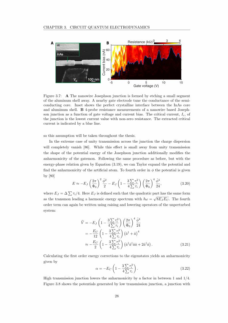
CHAPTER 3. CIRCUIT QUANTUM ELECTRODYNAMICS
A B
Gate voltage (V)-5 0 5 10 15
Curr
ent bia
s (
nA
)
0
20
40
60
0 3 6Resistance (kΩ)
Figure 3.7: A The nanowire Josephson junction is formed by etching a small segmentof the aluminum shell away. A nearby gate electrode tune the conductance of the semi-conducting core. Inset shows the perfect crystalline interface between the InAs coreand aluminum shell. B 4-probe resistance measurements of a nanowire based Joseph-son junction as a function of gate voltage and current bias. The critical current, Ic, ofthe junction is the lowest current value with non-zero resistance. The extracted criticalcurrent is indicated by a blue line.
so this assumption will be taken throughout the thesis.
In the extreme case of unity transmission across the junction the charge dispersion
will completely vanish [86]. While this effect is small away from unity transmission
the shape of the potential energy of the Josephson junction additionally modifies the
anharmonicity of the gatemon. Following the same procedure as before, but with the
energy-phase relation given by Equation (3.19), we can Taylor expand the potential and
find the anharmonicity of the artificial atom. To fourth order in φ the potential is given
by [80]
E ≈ −EJ
(2π
Φ0
)2φ2
2− EJ
(1− 3
∑τ2i
4∑τi
)(2π
Φ0
)4φ4
24, (3.20)
where EJ = ∆∑τi/4. Here EJ is defined such that the quadratic part has the same form
as the transmon leading a harmonic energy spectrum with ~ω =√8EJEC . The fourth
order term can again be written using raising and lowering operators of the unperturbed
system:
V = −EJ
(1− 3
∑τ2i
4∑τi
)(2π
Φ0
)4φ4
24
= −EC
12
(1− 3
∑τ2i
4∑τi
)(a† + a
)4
≈ −EC
2
(1− 3
∑τ2i
4∑τi
)(a†a†aa+ 2a†a
). (3.21)
Calculating the first order energy corrections to the eigenstates yields an anharmonicity
given by
α = −EC
(1− 3
∑τ2i
4∑τi
). (3.22)
High transmission junction lowers the anharmonicity by a factor in between 1 and 1/4.
Figure 3.8 shows the potentials generated by low transmission junction, a junction with
28

CHAPTER 3. CIRCUIT QUANTUM ELECTRODYNAMICS
φ-π -π/2 0 π/2 π
Energ
y / E
J
0
1
2
3
4
5
-EJcos(φ)
-4EJcos(φ/2)
EJ
2/2φ
Figure 3.8: Josephson junction potentials for a tunnel junction, a junction with unitytransmission, and their harmonic approximation in red, blue, and black respectively. Thetwo cosine potentials are offset to match the harmonic potential at φ = 0.
unity transmission, and a harmonic potential all with the same harmonic approximation.
Indeed we see that the unity-transmission potential more closely resembles the harmonic
potential leading to a lower anharmonicity.
3.4 Coupled Artificial Atoms and Harmonic Oscilla-
tors
With superconducting circuits acting as qubit we need a way to readout the state of the
qubit without introducing noise. This can be done by coupling a qubit to a harmonic
oscillator, which acts as a filter protecting the qubit from the environment while allowing
state readout [57, 87, 88]. An artificial atoms and harmonic oscillators can be coupled
through a capacitor Cg as shown in Figure 3.9. Here the resonator is modelled as a
lumped element LC circuit but the theory also applies to resonators formed in distributed
elements as shown in Figure 3.2. The qubit will have a separate coupling to each mode
of the distributed cavity, however in practice only one of the modes has a significant
coupling due to the energy separation.
The coupled circuit in Figure 3.9 has three flux nodes: φA, φr, and ground. Following
the same procedure as in section 3.1 the Lagrangian is found as
L = E(φA)−Cφ2A2
+φ2r2Lr
− Crφ2r
2− Cg(φr − φA)
2
2, (3.23)
where E(φA) is the potential energy of the Josephson junction. Assuming Cg ≪ Cr, C
29

CHAPTER 3. CIRCUIT QUANTUM ELECTRODYNAMICS
CEJ
Cg
Lr
Cr
φA
φr
Figure 3.9: Schematic of an artificial atom coupled capacitively to a harmonic oscillator.
the conjugate momenta of each coordinate can be written as6
QA =∂L∂φA
≈ CφA, (3.24)
Qr =∂L∂φr
≈ Crφr. (3.25)
Performing a Legendre transformation and promoting the coordinates and their conjugate
momenta to quantum operators yields the Hamiltonian of the system
H =1
2CQ2
A + E(φA) +1
2CrQ2
r +1
2Lφ2r +
Cg
CCrQrQA
= HA + Hr + Hg (3.26)
where HA and Hr are the Hamiltonians for the isolated atom and resonator circuits
respectively and Hg is the coupling term. It is convenient to describe the system using
eigenstates of the Hamiltonian with Hg = 0. In this case the eigenstates are simply
product states of the uncoupled qubit and resonator which can be described by raising
and lowering operators.
Focusing on the low-energy part of the atom spectrum we treat it as two-level, qubit
system. Using raising and lowering operators and Pauli operators for isolated resonator
and qubit respectively the Hamiltonian becomes7
H = ~ωra†a+ ~
ωq
2σz +
2eCg
C〈1|n|0〉VZPF(a+ a†)(σ+ + σ−), (3.27)
where VZPF = QZPF/Cr =√~ωr/2Cr are the voltage zero-point fluctuations of the
resonator8, n = QA/2e is the number of Cooper pairs on the qubit capacitor C, and |i〉are qubit states. Ignoring non-energy conserving terms in the coupling and collecting
6One finds a small modification to the effective capacitances of the resonator and artificial atomwithout this approximation as calculated in appendix of [58].
7We have changed the phase of the resonators raising and lowering operators a and a† as is conven-tional [58].
8For resonators formed in distributed elements VZPF is position dependent along the resonator andone needs to calculate VZPF(x) at the qubit position x.
30

CHAPTER 3. CIRCUIT QUANTUM ELECTRODYNAMICS
Figure 3.10: The energy spectrum of the Jaynes-Cummings Hamiltonian in the resonantregime with ωr = ωq. Left are the states |n, g〉 where n is the number of photons in theresonator and |g〉 is the ground state of the qubit. Adding a photon to the resonatorstates increases the energy by ~ωr. Right are states |n, e〉 where |e〉 is the excited stateof the qubit raising the energy by ~ωq. In blue are the eigenstates of the coupled systemdescribed by Equation (3.28).
factors as ~g =2eCg
C 〈1|n|0〉VZPF we arrive at the Jaynes-Cummings Hamiltonian:
H = ~ωra†a+ ~
ωq
2σz + ~g(aσ+ + a†σ−). (3.28)
There are two distinct regimes for the Jaynes-Cummings Hamiltonian. The resonant
regime when ωr = ωq and the dispersive regime with |ωq − ωr| ≫ g. In the resonant
regime the qubit and resonator states hybridize as shown in Figure 3.10. In the one
excitation manifold the eigenstates are superpositions of a photon in the resonator and
an excitation in the qubit. The splitting of the resonator state is known as the vacuum-
Rabi splitting as a qubit excitation does Rabi oscillations with the vacuum state of the
resonator. To observe the splitting we need g/π to be larger than the linewidth of both
the qubit and resonator. Observing vacuum-Rabi splitting demonstrates strong and
coherent qubit-resonator coupling but the regime is not suitable for quantum processing.
For quantum processing we want to be in the dispersive regime where the qubit
frequency is far detuned from the resonator frequency. This regime allows us to simplify
the Jaynes-Cummings Hamiltonian in Equation (3.28) by expanding to second order in
the small parameter g/∆, where ∆ = ωq − ωr is the detuning. One has to be careful
when doing the expansion as higher energy levels of the artificial atom are important.
Therefore the expansion is done on the full multilevel system and then truncated to a
two level system afterwards [67]. The total system of a multilevel artificial atom coupled
31

CHAPTER 3. CIRCUIT QUANTUM ELECTRODYNAMICS
|0,0〉
|1,0〉
|2,0〉
|1,1〉
|0,1〉
|0,2〉
|1,2〉
1
2
Figure 3.11: Energy spectrum of the Jaynes-Cummings Hamiltonian in the dispersiveregime shown in Equation (3.30). Energy states |n, j〉, where n is number of photons inthe resonator and j is the number of excitations on the transmon, depicted as black forcoupling off and dashed blue for coupling on. State |1, 1〉 couples to both states |0, 2〉and |2, 0〉 which gives a dispersive shift in opposite directions.
to a harmonic oscillator is described by the generalized Jaynes-Cummings Hamiltonian:
H = H0 + V , (3.29)
H0 = ~ωra†a+ ~
∑
i
ωi|i〉〈i|,
V = ~
∑
i
gi,i+1(a|i+ 1〉〈i|+ a†|i〉〈i+ 1|).
The coupling strength is given by gij =2eCg
~C 〈i|n|j〉VZPF. Here we assume that the
artificial atom is a transmon with EJ ≫ EC which leads to gij = 0 for i 6= i ± 1. For
other artificial atoms the matrix elements 〈i|n|j〉 can have very different selection rules.
The Hamiltonian can be simplified using second order perturbation theory treating the
interaction term V as a perturbation. Eigenstates for H0 are readily found as |n, j〉 wheren is the resonator photon number and j is the excitation level of the artificial atom. An
explicit calculation can be found in Appendix A leading to the Hamiltonian:
H =~
(ωr −
χ12
2
)a†a+ ~
1
2(ωq + χ01)σz + ~χa†aσz (3.30)
where χij = g2ij/(ωij − ωr) and χ = χ01 − χ12/2.9 Figure 3.11 depicts the lowest energy
levels of the Jaynes-Cummings Hamiltonian in the dispersive regime.
There are three terms in the Hamiltonian originating from the coupling. The first two
terms are called Lamb shifts giving a correction to the qubit and resonator frequencies.
9If the system is truncated before the approximation all terms with χ12 vanish as state |2〉 is absent.
32

CHAPTER 3. CIRCUIT QUANTUM ELECTRODYNAMICS
The last term can be interpreted in two ways. It can be viewed as a correction to the
qubit frequency dependent on the number of photons in the resonator [89]. This is known
as the Stark shift of the qubit and can be exploited to measure photon number states in
the resonator [60, 90]. Equally valid it can be interpreted as a qubit dependent dispersive
shift of the resonator:
H = ~ (ω′r + χσz) a
†a+ ~1
2ω′qσz, (3.31)
where ω′q = ωq + χ01 and ω′
r = ωr − χ12. Written in this form the Hamiltonian ex-
plicitly shows a qubit state dependent shift on resonance frequency of the resonator.
The dispersive shift in the transmon limit is given by χ = αg2/∆(∆ + α), where α
is the anharmonicity of the qubit. By probing the frequency of the resonator with a
classical microwave tone we can infer the qubit state. Furthermore, this is a quantum
non-demolition (QND) readout scheme as the qubit state is an eigenstate of the Hamilto-
nian, which means that the qubit is left in the measured state after readout [57]. This can
be exploited to perform qubit state preparation with fast measurement feedback [91, 92].
The resonator is coupled to the measurement apparatus leading to a photon decay
rate, κ, or the resonator. As the qubit is coupled to the resonator the photon decay will
induce a qubit decay known as the Purcell effect [93]. For large detuning the induced
qubit decay is given by γ ≈ (g/∆)2κ [88]. The speed of qubit readout is limited by κ,
the rate of photons leaking out to instruments, while qubit lifetime is limited by 1/κ.
Depending on the scope of the experiment one might need to suppress the Purcell effect
to allow for fast measurements without compromising qubit lifetimes [94–97].
3.5 Single Qubit Control
For qubit control we return to the simple transmon circuit capacitively coupled to a
voltage source [Figure 3.4] whose Hamiltonian is
H = 4EC n2 − EJ cos (ϕ) +
2eCg
CVg(t)n, (3.32)
where Vg(t) is separated as an individual term. Qubit operations are achieved by applying
an ac voltage Vg(t) = vR cos(ωt) + vI sin(ωt) where vR and vI are the in phase and out
of phase components of the voltage respectively. Writing the Hamiltonian in eigenstates
of the undriven artificial atom we have
H =∑
i
~ωi|i〉〈i|+∑
i,j
2eβ〈i|n|j〉 [vR cos(ωt) + vI sin(ωt)] (|j〉〈i|+ |i〉〈j|), (3.33)
where β = Cg/C. Focusing on a two-level subspace spanned by states |0〉 and |i〉 the
Hamiltonian can be written with Pauli operators:
H =~ωi
2σz,i + 2eβ〈0|n|i〉 [vR cos(ωt) + vI sin(ωt)] (σ+,i + σ−,i), (3.34)
33

CHAPTER 3. CIRCUIT QUANTUM ELECTRODYNAMICS
where σz,i = |i〉〈i| − |0〉〈0|, σ+,i = |i〉〈0|, and σ−,i = |0〉〈i|. In a rotating frame of the
drive and invoking the rotating wave approximation the Hamiltonian reduces to
HR = eiωtσz,i/2He−iωtσz,i/2 − ~ω
2σz,i
=~(ωi − ω)
2σz,i +
~
2[ΩR,iσx,i − ΩI,iσy,i], (3.35)
where Ωj,i =2e~β〈0|n|i〉vj are Rabi frequencies. A classical microwave signal V (t) on an
electrode capacitively coupled to the artificial atom can drive the system from |0〉 to |i〉and back with a frequency given by Ωj,i. With independent control of ΩR,i and ΩI,i we
can drive the two-level system around an arbitrary axis in the XY plane of the Bloch
sphere. For transmons with EJ ≫ EC the only non-zero matrix elements are 〈i|n|i+ 1〉allowing us to focus on just the 0-1 transition. However, as we will see in Chapter 6, more
exotic circuits can have tunable matrix elements leading to some transitions appearing
and disappearing as they are tuned.
For tunable transmons, e.g. gatemons, one can tune the qubit frequency. Limiting the
Hamiltonian to a truncated qubit subspace with resonance frequency ωq the Hamiltonian
of a gatemon can, in the rotating frame of the drive, be written as
HR =~
2[δq(Vc)σz +ΩRσx − ΩI σy], (3.36)
where δq(Vc) = ωq(Vc)−ω is the qubit-drive detuning and Vc is the control voltage tuning
EJ of the Josephson junction. With independent and fast control of all parameters δq,
ΩR, and ΩI we have complete control of the qubit system.
Here we considered a drive signal, Vg(t), applied to a nearby electrode capacitively
coupled to the artificial atom. Alternatively one might apply the drive signal through a
readout cavity coupled to the artificial atom. In this case the cavity will act as a filter
on the drive signal reducing the effective Rabi frequencies dependent on the cavity-qubit
coupling and detuning: Ωj = g∆
[2e~β〈0|n|i〉vj
], but otherwise behaves the same as a
direct capacitive coupling [58].
3.6 Two-Qubit Operations
For universal quantum processing we also need to engineer qubit-qubit interactions. For-
tunately, it is sufficient to have just one entangling two-qubit gate. For transmon qubits
there are several ways to implement two-qubit gates [98–101]. Here we will focus on one
of the most widely used two-qubit gates: the controlled phase gate (CZ gate) [102, 103].
The CZ gate performs a Z gate on a target qubit dependent on the state of a control
qubit. Implementations of two-qubit gates relies both on an engineered coupling and
control pulses used to perform the gate.
There are a multiple ways to engineer a qubit-qubit couplings for transmons. One
is a direct capacitive coupling that is very similar to the qubit resonator coupling [104]
while another is a coupling mediated by a resonator [105], which was used for the first
34

CHAPTER 3. CIRCUIT QUANTUM ELECTRODYNAMICS
C1
EJ1
EJ2
C2
Cg
Figure 3.12: Two transmon qubits coupled capacitively.
C1
EJ1
Cg2
EJ2
C2
Cg1
LrCr
Figure 3.13: Two transmon qubits coupled via a resonator.
demonstration of two-qubit operations in transmon qubits.
Two transmons can be coupled as shown schematically in Figure 3.12. Notice the
similarity of the circuit to that of a transmon coupled to a harmonic oscillator in Figure
3.9. Following the same procedure leading to the Jaynes-Cummings Hamiltonian in
Equation (3.28) but truncating both transmons to two-level systems it is straightforward
to find the Hamiltonian as
H = ~ω1
2σz,1 + ~
ω2
2σz,1 + ~J(σ−,1σ+,2 + σ+,1σ−,2), (3.37)
where ω1 and ω2 are the resonance frequencies of qubit 1 and 2 respectively and J =(2e)2Cg
C1C2〈0|1n1|1〉1〈1|2n2|0〉2 is the qubit-qubit coupling strength. In the transmon limit we
can write the coupling term as J =Cg
√ω1ω2
2√C1C2
. If the qubits are far detuned in frequency the
coupling term becomes negligible due to energy conservation. By pulsing the qubits into
resonance, for instance by changing the gate voltage on a nanowire Josephson junction,
one can turn on the coupling for a short time to perform a gate.
A somewhat more involved system is the qubit-resonator-qubit circuit shown in Figure
3.13. The Hamiltonian in the rotating wave approximation takes the form of a Jaynes-
Cummings Hamiltonian with qubit-resonator couplings for each qubit
H = ~ωra†a+ ~
∑
i
ωi
2σz,i +
∑
i
~gi(aσ+,i + a†σ−,i). (3.38)
This Hamiltonian is known as the Tavis-Cummings Hamiltonian and describes the cou-
pling of multiple qubits to a single harmonic mode. As for readout we want to be in the
dispersive limit where both qubits are far detuned from the resonator. In the dispersive
35

CHAPTER 3. CIRCUIT QUANTUM ELECTRODYNAMICS
limit where g1, g2 ≪ ∆1,∆2 the Hamiltonian can be written as [106]
H = ~ (ω′r + χ1σz,1 + χ2σz,2) a
†a+
2∑
i=1
~ω′i
2σz,i + ~g1g2
∆1 +∆2
2∆1∆2(σ+,1σ−,2 + σ−,1σ+,2),
(3.39)
where gi =2eCgi
Ci〈1|ini|0〉iVZPF and ∆i = ωi − ωr. The coupling term is the same as for
the direct coupling with a strength determined by the qubits’ coupling to the resonator
and how far detuned they are. When the two qubits are on resonance the coupling
strength is g1g2/∆.
Both implementations of qubit-qubit coupling lead to the same effective Hamiltonian.
Experimentally there are pros and cons of both layouts and the choice of coupling depends
on the specific experiments needs. A distributed coupling cavity allows extra space as
the qubits can be coupled over long distances. This suppresses any unwanted crosstalk
between qubits for single qubit gates as well as allowing extra space for control wirering
such as readout resonators and gate lines. On the other hand adding a cavity to mediate
the coupling also adds a decay channel as well as one more element that can fail during
fabrication.
The coupling between qubits in this implementation is a fixed coupling strength which
is dynamically turned on by pulsing the qubits into resonance. Figure 3.14 shows the
level spectrum for two coupled transmons. Blue lines are the single-excitation energies,
with an avoided crossing between states |01〉 and |10〉, while red shows two-excitation
energies and coupling between states |02〉 and |11〉. Two types of two-qubit gates can be
performed in this spectrum. One is an iSWAP gate performed by pulsing the energy of
the qubit 1 diabatically into the |10〉-|01〉 anticrossing for a certain time10:
iSWAP|00〉 = |00〉, iSWAP|11〉 = |11〉,iSWAP|01〉 = −i|10〉, iSWAP|10〉 = −i|01〉. (3.40)
The gate set of iSWAP and single qubit gates is in fact a universal gate set [107].
Unfortunately due to the low anharmonicity of a transmon qubit one has to consider
the effect of higher energy states shown in red. The coupling term in Equation (3.37) also
couples states |02〉 ↔ |11〉 and |20〉 ↔ |11〉. To avoid any leakage errors the pulse scheme
used to implemented two-qubit gates needs to suppress any |02〉 or |20〉 population after
each gate. This poses a problem for the iSWAP operation which requires a diabatic pulse
to bring the two qubits on resonance. Such a pulse will have to move through the avoided
crossing between states |02〉 and |11〉 (or |20〉 and |11〉), which will cause leakage errors
if the pulse is not fast enough. Experimentally it turns out to be challenging to avoid
any leakage leading experimenters to come up with another type of two-qubit gates in
transmons.
The idea is to take advantage of the |02〉 ↔ |11〉 anticrossing while avoiding any
leakage by clever pulse shaping [102]. A diabatic pulse into the |02〉 ↔ |11〉 anticrossing
10Such a pulse will also perform a single qubit phase operation which has not been included in thisdiscussion for simplicity. One can easily correct for the phase operation e.g. with a single qubit phaseoperation after the two-qubit operation.
36

CHAPTER 3. CIRCUIT QUANTUM ELECTRODYNAMICS
Qubit 1 Energy / h (GHz)4.6 4.8 5
Energ
y / h
(G
Hz)
4.4
4.6
4.8
5
Energ
y / h
(G
Hz)
9.4
9.6
9.8
10
Figure 3.14: Energy spectrum of two coupled transmons as a function qubit 1 energywith fixed energy for qubit 2. Blue (red) indicates the one-excitation (two-excitation)manifold with the energy shown on the left (right) axis. Qubit 2 has energy ω2/2π =5 GHz, the anharmonicity of both qubits is α/2π = −300 MHz, and coupling strengthJ/2π = 20 MHz.
will after a time implement a controlled phase (CZ) gate due to state oscillations of |11〉and |02〉:
CZ|00〉 = |00〉, CZ|11〉 = −|11〉,CZ|01〉 = |01〉, CZ|10〉 = |10〉. (3.41)
The CZ gate avoids the complexity of interacting with multiple anticrossings in the
same pulse. More recent implementations makes use of a fast adiabatic approach to the
avoided crossing keeping the state in an eigenstate at all times [103, 108]. Such a pulse
has the advantage of limiting leakage simply by making the pulse slower. Furthermore,
it is experimentally much easier to implement adiabatic pulses than diabatic due the the
limited bandwidth of control electronics and cabling.
37

Chapter 4
Fabrication and Experimental
Setup
4.1 Fabrication
Device fabrication of superconducting qubits is an extended process requiring several
advanced techniques. Furthermore, losses in superconducting qubits can easily be limited
by loss tangent of the materials and the quality of the materials interfaces formed during
fabrication [109–112]. Consequently, optimizing qubit lifetimes is a tight loop with the
fabrication processes.
For nanowire-based devices the fabrication is further complicated by the somewhat
random placement of the nanowire requiring manual design adjustments for each nano-
wire1. The individual steps of the process are fairly standard involving either e-beam or
UV lithography followed by a lift-off or etch-back process. A detailed list of processes for
each sample presented in this thesis can be found in Appendix D. The general process
flow of nanowire-based superconducting circuits can be divided into two stages: before
nanowire deposition and after nanowire deposition.
The first stage defines the large scale cQED circuits, e.g. resonators and qubit islands.
At this level every device is identical and can beneficially be fabricated simultaneously on
a single wafer. For small scale cleanrooms, such as the one used at Center for Quantum
Devices, 2” wafers containing a few tens of chips is a good compromise between parallel
fabrication and tool availability. As this stage is parallel fabrication of tens of devices
one wants to do as much of the fabrication as possible during this stage.
Before the second stage the wafer is cut up in smaller chips containing only a few
devices. Much of the work in this stage scales with the number nanowires rather than
the number of chips. The nanowire placement can be done in two fashions. A random
placement via a tissue transferring tens of nanowires from growth chip to device chip as
described in [114]. This is a fairly fast process but is rather uncontrolled. Alternatively
one can use a micromanipulator, which is a needle controlled to sub micrometer scale,
1This can be mitigated with image recognition software [113].
38

CHAPTER 4. FABRICATION AND EXPERIMENTAL SETUP
installed under a microscope to transfer individual nanowires from the growth chip to
desired location and orientation on device chip. This is a very tedious and time consuming
process but necessary if the placement of the nanowire is crucial, e.g. bottom gate
structures.
Following placement of InAs/Al core/shell nanowires a small segment of the shell
needs to be etched away to form Josephson junctions. The process resulting in best
nanowire etches during my work has been a 9-12 s, 50 C Transcene D etch2 with e-
beam lithography windows defined in PMMA directly followed by thorough rinsing in DI
water. While giving good results it is a very sensitive process with far from 100 % yield.
4.2 Experimental Setup
Detailed schematics of the each setup used are given in Appendix C.
Superconducting qubit devices are very sensitive to radiation both at the qubit fre-
quency and in THz (infrared light) frequencies leading to quasiparticle excitations. It
is therefore crucial to properly shield devices from any black-body radiation of higher
temperature stages [115, 116]. This is commonly done by multiple closed boxes with light
absorbing coatings. Any residual light entering a box should be absorbed far away from
the device. For measurements in Chapters 5 and 6 we use an aluminium box inside a
copper box both coated by light-absorbing paint. The box for high-field compatibility in
Chapter 7 is made of CuBe and filled with light absorbing foam. Similarly any electrical
connection to the device is carefully filtered or heavily attenuated.
Throughout the thesis three measurement techniques are used to probe the devices:
• Single-tone spectroscopy: the frequency response of the readout resonator is
measured with a vector network analyser.
• Two-tone spectroscopy: the resonator is monitored by a ‘readout’ tone at a fixed
frequency while a second ‘drive’ tone is swept. When the drive tone is on resonance
with the qubit it will induce excitations leading to a peak in the transmission of
the monitored readout tone.
• Time-domain measurements: A drive tone is turned on for a controlled time in-
ducing rotations of the qubit state followed by a readout tone probing the resonator
transmission.
Two-tone spectroscopy is a fairly time-consuming measurement both due to the
amount of data taken and due to slow sweeping of drive tone frequency. Most mi-
crowave signal generators are fairly slow at changing frequency leading to a great deal
of ‘dead time’, where no measurements are performed. For faster data acquisition we
take advantage of features on a Rhode & Schwarz ZNB vector network analyser (VNA)
allowing to decouple output frequency and measurement frequency. A VNA is optimized
for frequency sweeping, which we utilize for the drive tone while the VNA monitors the
response of the readout tone at a fixed frequency. For a VNA with 4 ports the unit can
2Etch time is dependent on shell thickness: 9 s for 7 nm half shell and 12 s for 30 nm thick full shell.
39

CHAPTER 4. FABRICATION AND EXPERIMENTAL SETUP
output two tones: one is set to a fixed readout frequency probing transmission of the
resonator while the second tone is swept to probe the qubit frequency. For a VNA with
2 ports the unit can output one tone which is used to probe the qubit frequency. The
readout tone is measured by the VNA but generated by a separate Rhode & Schwarz
SGS100A signal generator.
For measurements affecting the resonance frequency of the readout resonator it is
essential to continuously adjust the frequency of the readout tone. As both single-tone
spectroscopy, probing the resonator frequency, and two-tone spectroscopy is performed
by the VNA one can swap between each technique in software. This allows one to first
probe the resonator and adjust the readout frequency used in two-tone spectroscopy
without substantially extending the measurement time.
All time domain measurements are controlled by a Tektronix AWG 5014C. The arbi-
trary waveform generator (AWG) handles the envelopes of RF signals by IQ modulation
of vector signal generators controlling the amplitude of the in phase and out of phase
components. With the RF signal on resonance with the qubit each component corre-
sponds to ΩR(t) and ΩI(t) in equation 3.36, which rotates the qubit around x and y axis
of the Bloch sphere. For high fidelity gates further pulse modulation, in addition to IQ
modulation, of the signal generator is used to reduce residual microwave leakage in the
nominally off-state. A line from the AWG is combined with a DC voltage source via an
RC bias-T either at room temperature or at base temperature for nanosecond control of
the gate voltage controlling EJ . Similarly to the qubit dive the output of the readout
tone is modulated by the AWG. It is measured with heterodyne demodulation by first
down converting the signal to an intermediate frequency (10 − 30 MHz) and then mea-
sured by an AlazarTech ATS9360 waveform digitizer followed by digital demodulation
[117].
40
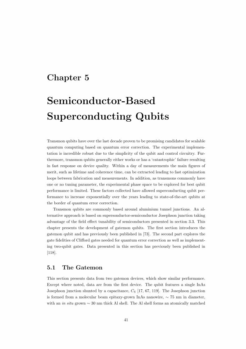
Chapter 5
Semiconductor-Based
Superconducting Qubits
Transmon qubits have over the last decade proven to be promising candidates for scalable
quantum computing based on quantum error correction. The experimental implemen-
tation is incredible robust due to the simplicity of the qubit and control circuitry. Fur-
thermore, transmon qubits generally either works or has a ‘catastrophic’ failure resulting
in fast response on device quality. Within a day of measurements the main figures of
merit, such as lifetime and coherence time, can be extracted leading to fast optimization
loops between fabrication and measurements. In addition, as transmons commonly have
one or no tuning parameter, the experimental phase space to be explored for best qubit
performance is limited. These factors collected have allowed superconducting qubit per-
formance to increase exponentially over the years leading to state-of-the-art qubits at
the border of quantum error correction.
Transmon qubits are commonly based around aluminium tunnel junctions. An al-
ternative approach is based on supersonductor-semiconductor Josephson junction taking
advantage of the field effect tunability of semiconductors presented in section 3.3. This
chapter presents the development of gatemon qubits. The first section introduces the
gatemon qubit and has previously been published in [73]. The second part explores the
gate fidelities of Clifford gates needed for quantum error correction as well as implement-
ing two-qubit gates. Data presented in this section has previously been published in
[118].
5.1 The Gatemon
This section presents data from two gatemon devices, which show similar performance.
Except where noted, data are from the first device. The qubit features a single InAs
Josephson junction shunted by a capacitance, CS [17, 67, 119]. The Josephson junction
is formed from a molecular beam epitaxy-grown InAs nanowire, ∼ 75 nm in diameter,
with an in situ grown ∼ 30 nm thick Al shell. The Al shell forms an atomically matched
41
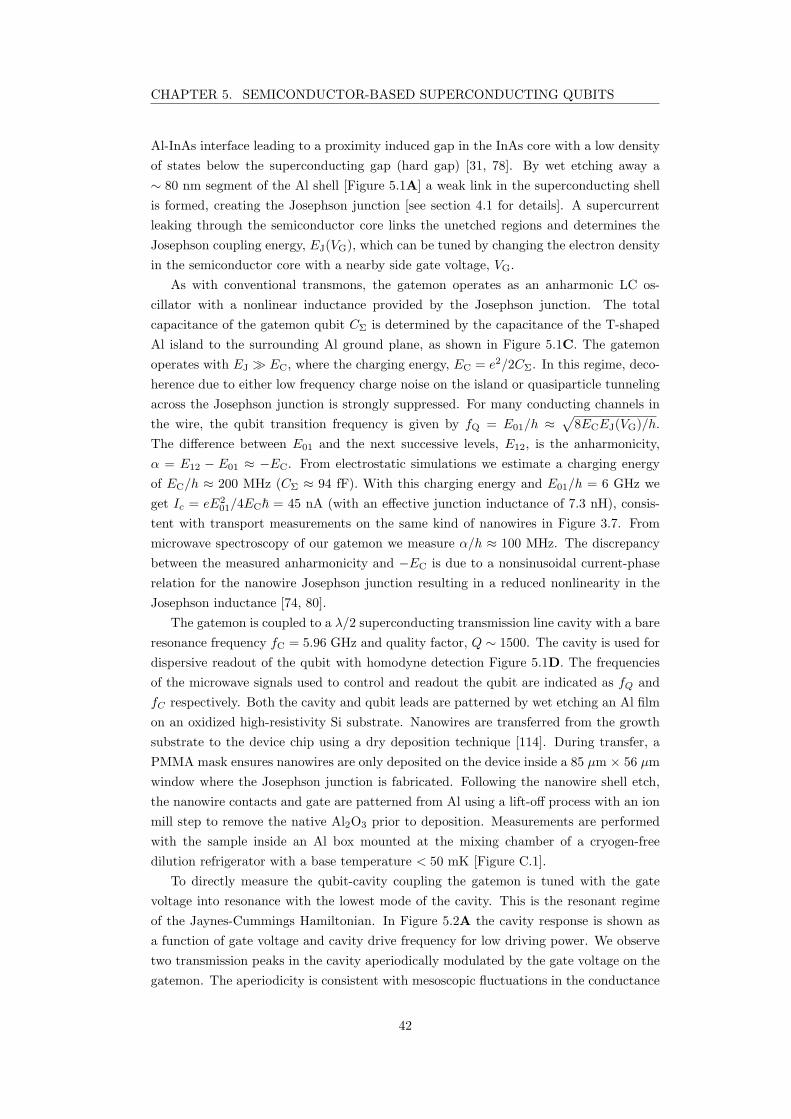
CHAPTER 5. SEMICONDUCTOR-BASED SUPERCONDUCTING QUBITS
Al-InAs interface leading to a proximity induced gap in the InAs core with a low density
of states below the superconducting gap (hard gap) [31, 78]. By wet etching away a
∼ 80 nm segment of the Al shell [Figure 5.1A] a weak link in the superconducting shell
is formed, creating the Josephson junction [see section 4.1 for details]. A supercurrent
leaking through the semiconductor core links the unetched regions and determines the
Josephson coupling energy, EJ(VG), which can be tuned by changing the electron density
in the semiconductor core with a nearby side gate voltage, VG.
As with conventional transmons, the gatemon operates as an anharmonic LC os-
cillator with a nonlinear inductance provided by the Josephson junction. The total
capacitance of the gatemon qubit CΣ is determined by the capacitance of the T-shaped
Al island to the surrounding Al ground plane, as shown in Figure 5.1C. The gatemon
operates with EJ ≫ EC, where the charging energy, EC = e2/2CΣ. In this regime, deco-
herence due to either low frequency charge noise on the island or quasiparticle tunneling
across the Josephson junction is strongly suppressed. For many conducting channels in
the wire, the qubit transition frequency is given by fQ = E01/h ≈√8ECEJ(VG)/h.
The difference between E01 and the next successive levels, E12, is the anharmonicity,
α = E12 − E01 ≈ −EC. From electrostatic simulations we estimate a charging energy
of EC/h ≈ 200 MHz (CΣ ≈ 94 fF). With this charging energy and E01/h = 6 GHz we
get Ic = eE201/4EC~ = 45 nA (with an effective junction inductance of 7.3 nH), consis-
tent with transport measurements on the same kind of nanowires in Figure 3.7. From
microwave spectroscopy of our gatemon we measure α/h ≈ 100 MHz. The discrepancy
between the measured anharmonicity and −EC is due to a nonsinusoidal current-phase
relation for the nanowire Josephson junction resulting in a reduced nonlinearity in the
Josephson inductance [74, 80].
The gatemon is coupled to a λ/2 superconducting transmission line cavity with a bare
resonance frequency fC = 5.96 GHz and quality factor, Q ∼ 1500. The cavity is used for
dispersive readout of the qubit with homodyne detection Figure 5.1D. The frequencies
of the microwave signals used to control and readout the qubit are indicated as fQ and
fC respectively. Both the cavity and qubit leads are patterned by wet etching an Al film
on an oxidized high-resistivity Si substrate. Nanowires are transferred from the growth
substrate to the device chip using a dry deposition technique [114]. During transfer, a
PMMA mask ensures nanowires are only deposited on the device inside a 85 µm × 56 µm
window where the Josephson junction is fabricated. Following the nanowire shell etch,
the nanowire contacts and gate are patterned from Al using a lift-off process with an ion
mill step to remove the native Al2O3 prior to deposition. Measurements are performed
with the sample inside an Al box mounted at the mixing chamber of a cryogen-free
dilution refrigerator with a base temperature < 50 mK [Figure C.1].
To directly measure the qubit-cavity coupling the gatemon is tuned with the gate
voltage into resonance with the lowest mode of the cavity. This is the resonant regime
of the Jaynes-Cummings Hamiltonian. In Figure 5.2A the cavity response is shown as
a function of gate voltage and cavity drive frequency for low driving power. We observe
two transmission peaks in the cavity aperiodically modulated by the gate voltage on the
gatemon. The aperiodicity is consistent with mesoscopic fluctuations in the conductance
42

CHAPTER 5. SEMICONDUCTOR-BASED SUPERCONDUCTING QUBITS
C
A B
Cavity
100 μm
10 μmVG
100 nmVG
EJ(V
G)C
S
Cavity
Cavity
drive
Qubit
VH
D
VG
InAs
Al
Qubit
drive
Figure 5.1: A The nanowire Josephson junction integrated into a transmon circuit.B The nanowire is contacted at each end and a nearby gate electrode can tune theJosephson energy of the junction. C The transmon is formed by a T-shaped islandshorted to the surrounding ground plane through the nanowire Josephson junction. Thetransmon circuit is closed by the capacitance of the island to ground. The island iscapacitively coupled to a λ/2 microwave cavity for readout. D Schematic of the gatemoncircuit.
43

CHAPTER 5. SEMICONDUCTOR-BASED SUPERCONDUCTING QUBITS
of the nanowire junction. The two peaks are the hybridized cavity-gatemon states [66].
Two widely split peaks, Figure 5.2B, indicate a cavity-gatemon in the strong coupling
regime with g larger than both the decay rate of the qubit and the cavity. Off resonance
the qubit-cavity states are very weakly hybridized and we only observe one peak, the
cavity resonance.
To better estimate the coupling strength g we extract the peak splitting δ for each
voltage value with two peaks in 5.2A. The hybridized states, f±, can be calculated from
the coupling strength g,
f± =fQ + fC ±
√(fQ − fC)2 + 4(g/2π)2
2, (5.1)
where fC and fQ are the frequencies of the uncoupled cavity and qubit respectively. By
plotting the peak splitting δ = f+−f− =√(fQ − fC)2 + 4(g/2π)2 as a function of fQ as
shown in Figure 5.2C we extract a coupling strength g/2π = 99 MHz. Plotting the data
in 5.2A parametrically as a function of the extracted fQ the expected avoided crossing
of a coupled two-level system is revealed in Figure 5.2D.
To perform coherent operation on the gatemon, we detune it away from the cavity
frequency to the dispersive regime. While continuously monitoring the cavity transmis-
sion at the cavity frequency we sweep a second microwave tone to drive the qubit. When
the qubit drive, the second tone, hits the resonance frequency of the qubit, the qubit is
excited into an incoherent superposition of |0〉 and |1〉 which modulates the monitored
cavity transmission. By sweeping the frequency of the qubit drive and the gate voltage
we map out the spectrum of the gatemon in Figure 5.3. In the spectrum we directly
observe the aperiodic modulation of the gatemon frequency originating from mesoscopic
fluctuations in the nanowire. These fluctuations create local minima and maxima that
are first-order insensitive to gate voltage (sweet spots). We also observe discontinuous
jumps in the spectrum that we attribute to charge traps near the nanowire changing the
charge landscape. Such jumps rarely happen when the gate voltage is restricted to a
small voltage range.
Figure 5.4A shows a scan of the qubit spectrum around the sweet spot at 3.4 V. Here
spectroscopy is performed by first applying a 2 µs long qubit drive tone and then probing
the cavity response to avoid Stark shift in the data. To perform qubit operations on the
gatemon we fix the gate voltage at 3.4 V indicated by B. In the top panel of Figure
5.4B the pulse scheme for Rabi oscillations is shown. First a qubit drive tone of length τ
rotates the qubit about the X axis and then a readout tone measures the probability for
the qubit to be in the |1〉 state. The lower part of the main panel shows Rabi oscillations
as the qubit is rotated around the Bloch sphere. When the qubit drive is detuned from the
resonance frequency the qubit does not fully reach the |1〉 state as seen in the amplitude
of the oscillations. The rotation axis is the combination of the drive strength along the
X axis plus a constant σz contribution due to the detuning (see equation (3.36)). This
also causes a faster oscillation frequency. By sweeping the drive time and drive detuning
we can see the effect as the Chevron pattern in the main panel.
While drive pulses around an axis in the XY plane are enough to perform all single
44

CHAPTER 5. SEMICONDUCTOR-BASED SUPERCONDUCTING QUBITS
0-5-1020log( VH
) (a.u.)
5.8
5.9
6.0
6.1
Cavity d
rive
(G
Hz)
VG
(V) 96 VH
(a.u.)0 0.2
δ
875
5.8 5.9 6.0 6.1
220
δ (M
Hz)
200
240
fQ
(GHz)
g/π
fQ
(GHz)
5.8
5.9
6.0
6.1
Cavity d
rive
(G
Hz)
5.8 5.9 6.0 6.1
A
DC
δ
B
fC
fC
fQ
g/π
fQ (V
G)
f-
f+
Figure 5.2: A Hybridization of the microwave cavity and gatemon qubit. Extractedqubit frequency and cavity frequency shown as green and blue lines respectively. B Linecut of A indicated by purple arrows. Clearly separated peaks in the transmission. C
The vacuum Rabi splitting as a function of extracted qubit frequency. D Parametricplot of the vacuum Rabi splitting as a function of extracted qubit frequency reveals theexpected anticrossing of two hybridized states.
VG
(V)3.4 3.6 3.8 4 4.2 4.4 4.6
Qu
bit d
rive
(G
Hz)
3.8
4
4.2
4.4
4.6
4.8
5
0 0.25 0.5Normalized transmission (dB)
Figure 5.3: Spectroscopy measurements of the qubit frequency as a function of gatevoltage. Each column is normalized by the value at 3.8 GHz.
45

CHAPTER 5. SEMICONDUCTOR-BASED SUPERCONDUCTING QUBITS
A
CB
Qubit d
rive (
GH
z)
VG (V)
VH (a.u.)
τ (ns)
p|1〉
0 100 2000
10
10
20
30
4.48
4.50
4.52
0 1
0 500 10000
1
τ (ns)
ΔVG (
mV
)
p|1〉
3.2 3.3 3.4 3.5
4.5
4.6
4.7
0 1
Qubit d
rive (
GH
z)
B
C
fQ = 4.507 GHz ΔV
G = 20.9 mV
|1〉
|0〉
fQ
VG
fC
Readout
p|1〉
|1〉
|0〉
fQ
fC
Readout
TimeΔV
G
ττ
Time
RX
π/2 RX
π/2
RZ
θRX
θR
X
θR
Z
θ
Figure 5.4: A Spectroscopy of the gatemon. B Upper panel shows the pulse sequence forqubit rotations around the X axis on the Bloch sphere. Main panel shows Rabi oscillationsas a function of drive time τ and qubit drive frequency. Lower panel is a line cut at thequbit frequency. C The pulse sequence for Z rotations is shown in the upper panel. Mainpanel shows rotations as a function of drive time τ and gate pulse amplitude. Lower panelis a line cut at pulse amplitude ∆VG = 20.9 mV. Normalized state probability, p|1〉, iscalculated from the demodulated cavity response, VH , by fitting Rabi oscillations toan exponentially damped sinusoid of the form V 0
H +∆VH exp (−τ/TRabi) sin(ωτ + φ) togive p|1〉 = (VH − V 0
H)/2∆VH + 1/2. The solid curves in lower panels of A and B areexponentially damped sinusoids.
46

CHAPTER 5. SEMICONDUCTOR-BASED SUPERCONDUCTING QUBITS
qubit operations it is convenient to have fast control of the qubit frequency to perform
two-qubit operations. To show that the gatemon allows fast adiabatic pulses of the
qubit frequency we measure the effect on a single qubit. Changing the qubit frequency
effectively induces Z rotations on the Bloch sphere. The qubit response is simplified
by placing the gate voltage at 3.27 V (indicated by C in Figure 5.4A) where the qubit
frequency depends linearly on the gate voltage. This ensures that the rotations induced
by the change in frequency depend linearly on the gate voltage. To observe rotations
about the Z axis, we first rotate the qubit by π/2 to the equator of the Bloch sphere
as shown in the upper panel of Figure 5.4C. Then a gate pulse of length τ induces a
rotation around the Z axis with a frequency proportional to the pulse amplitude (due to
the linear energy spectrum). A final π/2-pulse allows effective readout along the Y axis
of the Bloch sphere. In the main panel we see the rotations that depend on the length
of the pulse and the amplitude of the voltage pulse on the gate demonstrating coherent
voltage-pulse operations. Furthermore, these operations demonstrate the stability of the
gatemon as the data in the main panel of Figure 5.4B were collected over several hours.
In Figure 5.5 coherence measurements of two gatemon qubits are shown. The pulse
schemes for measuring the lifetime T1 and dephasing time T ∗2 are shown in black and
blue respectively. Lifetime is measured by varying the delay time between a π pulse,
which rotates the qubit to the |1〉 state, and readout. The expected exponential decay
with a characteristic time T1 of the |1〉 state probability is observed. We extract lifetimes
0.56 µs and 0.83 µs for sample 1 and 2 respectively.
The dephasing time is measured by placing the qubit on the equator with a slightly
detuned π/2 pulse so that the qubit state precesses around the equator. Readout is done
after a delay time τ and a second π/2 pulse to rotate the Y axis onto the Z axis for
readout. We observe the precession of the qubit as the oscillation while the exponential
decay with a characteristic time scale T ∗2 is due to decoherence. Lifetime enforces an
upper limit on the decoherence time of T ∗2 ≤ 2T1 as the qubit can decay from the
superposition state on the equator. For Sample 1 we find T ∗2 = 0.97 µs very close to the
lifetime limit. Sample 2 performs slightly worse with T ∗2 = 0.71 µs. For drifts in the
qubit frequency that are constant within the time of the pulse sequence one can cancel
the effect by performing an echo pulse as indicated in red. The pulse effectively reverses
the sign on the noise such that noise picked up before the echo pulses is cancelled by
noise after the pulse. High frequency noise switching faster than the sequence length will
not get cancelled by an echo pulse. More elaborate pulse schemes can be used to avoid
specific parts of the noise spectrum in the system [120]. We can increase the decoherence
time of qubit 2 to TEcho = 0.95 µs with an echo pulse. The fact that we do not reach the
lifetime limit indicates that qubit 2 suffers from some high frequency noise.
Lifetime and coherence times in this first generation of devices is primarily limited
by materials loss in the capacitors. Especially a ∼ 87 nm thick thermal oxide layer on
the silicon substrate leads to losses in capacitors. The oxide layer is initially included
to ensure electrical separation between the gate electrodes and the surrounding ground
plane. Subsequent studies reveal that a certain distance between contacts and gate
electrodes sufficiently insulates the electrodes (for ∼ 1 µm substrate leakage happens at
47

CHAPTER 5. SEMICONDUCTOR-BASED SUPERCONDUCTING QUBITS
0
1
p|1〉
0
1
p|1〉
1 20τ (μs)
0.5 1.5 1 20τ (μs)
0.5 1.5
τReadout
fQ
fC
RX
π
τReadout
fQ
fC
RX
π/2R
X
π RX
π/2
Rφπ/2
A
B
T1 = 0.56 μsSample 1
Sample 2 T1 = 0.83μs T
Echo = 0.95 μs
T2 = 0.73 μs*
T2 = 0.91 μs*
Sample 2
Sample 1
Figure 5.5: A Left shows lifetime measurement of sample 1 at point B in Figure 5.4A(VG = 3.4 V). Left side in upper panel shows the pulse scheme for lifetime measurements.A 30 ns π pulse rotates the qubit to the |1〉 state and a wait time τ before readout is varied.Solid curve is an exponential fit. Right side shows a Ramsey experiment performed byvarying a wait time τ between two slightly detuned 15 ns π/2 pulses. Solid curve is anexponentially damped sinusoid from which we determine T ∗
2 . B Lifetime and Ramseyexperiments are repeated for sample 2 which has fQ = 4.426 GHz (VG = −11.3 V).Furthermore we perform a Hahn echo experiment in red with a π pulse inserted betweentwo π/2 pulses with a varying wait time τ . The phase of the second π/2 pulse is variedto fit an exponential decay to the extracted amplitude.
48

CHAPTER 5. SEMICONDUCTOR-BASED SUPERCONDUCTING QUBITS
∼ ±10 V on gates) allowing for removal of the global thermal oxide. This combined with
careful optimization of capacitor loss in resonator Q-factor measurements lead to almost
tenfold increase in lifetime for second generation [118] of gatemons. Recent studies has
shown coherence times of gatemons approaching that of state-of-the-art transmon qubits
[113] demonstrating the feasibility for quantum-error correction with gatemon qubits.
5.2 Gatemon Benchmarking and Two-Qubit Opera-
tions
For quantum computations based on gatemons we want to quantify the fidelity of qubit
gates including two-qubit gates. To demonstrate two-qubit gates the second generation
is designed with two capacitively coupled gatemons [32]. Additionally, several improve-
ments are made in the design layout [Figure 5.6] and fabrication. Separate qubit drive
lines labelled ’XY control’ for individual qubit control, separate λ/4 readout cavities with
resonance frequencies fC1 = 7.81 GHz and fC2 = 7.73 GHz coupled to the same feed-
line for frequency-multiplexed readout, low loss substrate for reduced capacitor loss, and
control circuitry with added crossovers to reduce spurious modes in the ground plane
[110]. The qubit parameters differ only slightly from the first generation of gatemons
with simulated values of charging energy EC/h = 230 MHz and qubit-cavity coupling
g/2π ≈ 100 MHz. Electrostatic simulations predict a qubit-qubit coupling strength
J ∼ 20 MHz.
With the improvements we measure almost tenfold improvements for qubit lifetimes
up to T1 ∼ 5 µs and decoherence times T ∗2 ∼ 4 µs, which can with a single refocusing pulse
be increased to TEcho ∼ 9.5 µs almost at the limit of 2T1. Next we quantify the fidelity of
qubit operations with randomized benchmarking. We expect microwave induced gates to
have the same performance as other transmons as the capacitive coupling to the system
is independent of the Josephson junction. However, Z and Z/2 gates can be induced by
baseband pulsing of the junction gate changing EJ(VG). We want to verify high fidelity
of microwave induced gates and test the fidelity of qubit gates induced by voltage pulses.
Complete information of a qubit operation can be measured with quantum process
tomography [121], which describes how any input qubit state is processed by the qubit
operation to a qubit output state. However, each process matrix for just a single qubit
operation requires measuring 12 independent numbers with high precission1 [122]! Evi-
dently it is not practical to fully characterize a set of quantum operations due to time-
constraints. Rather we need a procedure that faithfully estimates the fidelity of gates in
an efficient manner.
For this purpose randomized benchmarking [123] has been adopted as a standard for
quantifying error rates of Clifford gates. Randomized benchmarking is done by measuring
the fidelity of a sequence of m random Clifford gates composing the identity operation.
From the decay of the fidelity of random sequences composing the identity operation as
1It is especially difficult to separate the qubit operation fidelity from errors in initialization andmeasurements.
49

CHAPTER 5. SEMICONDUCTOR-BASED SUPERCONDUCTING QUBITS
Q1 Q2XY control XY control
cavity 1 cavity 2
C12
V1 V2
200 µm
Figure 5.6: Optical image of a two qubit gatemon device. The two qubits are coupledto individual λ/4 cavities. Coherent operations are performed by drive lines coupledcapacitively to the gatemons.
a function of m one can extract an average error rate of all Clifford gates. Furthermore,
interleaved randomized benchmarking, which interleaves a specific Clifford gate between
each random gate of a sequence, allows measurement of error probability of individual
gates. Random Clifford gates will randomize the qubit state throughout the sequence ef-
fectively mapping any noise onto the depolarization channel. The depolarization channel
is fully described by a single probability, 1− p, that the qubit state is replaced with fully
mixed state [39]. The decay rate of fidelity is given by pm (the probability that the qubit
has not been replaced by a mixed state after m operations) and the average gate error
is r = (1 − p)/2.2 Importantly as the measurement relies of the decay rate of fidelity it
becomes independent of errors in state preparation and measurement (SPAM errors).
Figure 5.7 shows data from interleaved randomized benchmarking on Q2. First a
reference of non-interleaved randomized benchmarking is performed using only microwave
induced pulses. Black diamonds is the fidelity of pulse sequences comprising m random
Clifford gates, C, followed by a recovery pulse, CR, such that CR(C)m = I. As the full
sequence composes the identity the fidelity can be measured as the |0〉-state population.
Each Clifford gate is generated by one or more Gaussian shaped microwave pulses with
standard deviation σ = 7 ns and truncated to a full gate time of tg = 28 ns. These
pulses were optimized using AllXY pulse sequences [106] and randomized benchmarking
sequences [108]. The fidelity decays is fitted to Apmref + B with A = 0.53 and B = 0.42
accounting for SPAM errors. From pref = 0.981 we extract an average single-qubit error
rate of rref = (1− pref)/(2× 1.875) = 0.5± 0.07 %, where the factor 1.875 is the average
number of single qubit gates per Clifford gate.
For interleaved randomized benchmarking of gate G we measure the fidelity of pulse
2The factor 2 originates from the fact that a fully mixed state can only be in two states whenmeasured: one where an error occurred and one where no error occurred. So half the time no errorhappened even if the qubit was replaced by a mixed state.
50
CHAPTER 5. SEMICONDUCTOR-BASED SUPERCONDUCTING QUBITS
1.0
0.9
0.8
0.7
0.6
0.5
0.4
ytile
diF
806040200
m - number of Cliffords
0.8
0.6
0.4
0.2
0.0
r (%)
Ref Id X Y X/2 Y/2 Z Z/2
C
m
CR
Cm
CRG
Reference
Interleaved gate
Figure 5.7: Randomized benchmarking of single-qubit Clifford gates on Q2. Blackshows reference of randomized benchmarking of Clifford gates yielding an error rate ofr = 0.5 ± 0.07 %. Interleaved randomized benchmarking of individual gates revealsno discrepancy between microwave induced gates (gray) and baseband pulsing of gatevoltage VG2 (blue and red). Inset shows extracted error rates from each interleaved gate.
sequences comprising of CR(GC)m = I, where C again is random Clifford gates and
CR is the recovery pulse such that the total sequence composes identity. Measuring the
decay of fidelity as a function of m we again fit the decay to ApmG + B and extract pG
for each gate tested. From pg and pref the average gate error for gate G is given by
rg = (1 − pG/pref)/2. Inset in Figure 5.7 displays the error rates of individual gates.
Qubit gates induced by voltage pulses, Z and Z/2, are performed by a 28 ns square pulse
and reaches error rates of rZ = 0.35 ± 0.19% and rZ/2 = 0.18 ± 0.15% consistent with
the lifetime limit on gate error: rlimit = tg/3T1 = 0.3% [124], where T1 = 3.1 µs at the
measurement point. This clearly demonstrates that high fidelity gates can be performed
with gate voltage pulses in gatemon qubits.
Next we investigate coherent two-qubit operations. The qubit-qubit coupling is ob-
served in two-spectroscopy as an avoided crossing as the Q1 is swept through resonance
with Q2 [Figure 5.8A]. To demonstrate that we have coherent control of the two-qubit
system we perform iSWAP operations. The applied pulse sequence is shown in 5.8B.
With the qubits initially off-resonance a single π pulse excites Q2 to the |1〉 state while
Q1 is left in the ground state. A gate voltage pulse with amplitude ∆V2 on Q2 brings the
qubits diabatically into resonance for a time τ before bringing the system back for read-
out. The excitation initially on Q2 begins to oscillate between the hybridized qubits with
a frequency J/π. The |1〉 state probability in Q1 after an iSWAP operation is mapped
out as a function of waiting time τ and pulse amplitude ∆V2 in Figure 5.8C. A chevron
pattern is observed as the excitation coherently swaps between Q1 and Q2. A similar
plot is obtained for measurements of the |1〉 state probability of Q2 which is inverted
compared to 5.8C. In 5.8D a line trace of both measurements is shown demonstrating the
excitation swapping between the two qubits. From the oscillations we extract a coupling
51

CHAPTER 5. SEMICONDUCTOR-BASED SUPERCONDUCTING QUBITS
0.50.0
-0.5
140120100806040
2.01.0
1401201008060405.64
5.62
5.60
5.58
Qubit d
rive (
GH
z)
-3.80 -3.78 -3.76
V1 (V)
0 1| VH1 | + | VH2 | (a.u.)A B
D
0
0.5
1
P
20015010050
(ns)
Q1 Q2
V2
time
C
X
200
150
100
50
(n
s)
0.150.140.130.12
V2 (V)
0 1 P
Q1Q2
Q1
Q2
Q1
V2
1
1
Figure 5.8: A An avoided crossing is observed in spectroscopy measurements as thefrequency of Q1 is being swept through the frequency of Q2. B Pulse sequence formapping the qubit-qubit coupling in time domain. Q2 is excited by a π pulse followed bya gate pulse with amplitude ∆V2 and width τ . C Swap oscillations as a function of ∆V2and width τ . D Line cut of C with the gate pulse bringing the qubits into resonance fortime τ .
strength of 17.8 MHz.
The preferred two-qubit gate for quantum algorithms is a controlled phase gate cπZgate presented in section 3.5. To demonstrate the effect of the gate Q1 is used as control
qubit in either state |0〉 or |1〉 shown in blue and red respectively in Figure 5.9A. First
Q2 is placed on the equator of the Bloch sphere by a X/2 pulse to detect rotations
around the Z axis. Then a voltage pulse on Q2 brings the system close to the |20〉 − |11〉anticrossing acquiring a phase shift conditional on the state of Q1. Lastly, the acquired
phase is measured by varying the angle of a π/2 pulse before readout. The pulse sequence
is adjusted such that the dynamical phase acquired by Q2 due to the change in frequency
is a multiple of 2π. Performing the sequence with the control qubit in |0〉 and |1〉 we
find the conditional phase difference. Figure 5.9B shows the π phase dependence of the
control qubit as desired for the cπZ gate.
To estimate the gate fidelity we perform interleaved single-qubit randomized bench-
marking treating the cπZ gate as a single qubit Z gate as shown in 5.9C. The resulting
gate fidelity of cπZ with the state of the control qubit randomized between |0〉 and |1〉 isr = 9± 2 % [Figure 5.9D]. Fixing the state of the control qubit leads to similar gate fi-
delities as shown in the figure inset. We estimate a 4 % error rate due to qubit relaxation
and attribute the remaining 5 percentage points to leakage into state |20〉.
52

CHAPTER 5. SEMICONDUCTOR-BASED SUPERCONDUCTING QUBITS
time
1.0
0.5
0.0
P2
Q
0 /2 3 /2 2
Q1 1 Q1 0
-0.8-0.40.00.40.8
0.9
0.8
0.7
0.6
0.5
Fid
elit
y
108642m - number of Cliffords
10
5
r (%)
0 1 random
Q1 state
time
Q1 (control)
Q2 (target) Q2 (target)
Q1 (control)
V2 V2 c Z
X X X
X/2
1
0
1 0
0
C
m
CRcZ
R ( /2)
0
0
0
0
0
cZ
C
2
2011
10+01
V
1
A B
C D
Figure 5.9: A Pulse sequence to probe phase shift of controlled phase gate cπZ . Controlqubit is placed in either state |0〉 or |1〉 shown in blue and red respectively. To observea phase shift on target qubit Q2 it is placed on the equator by a X/2 pulse beforethe cπZ gate is performed. Lastly a π/2 gate along an axis whose phase θ is varied.B Probability of Q2 in state |1〉 as a function of θ. C Pulse scheme for interleavedrandomized benchmarking of the controlled phase gate cπZ . D Fidelity of interleaved,single-qubit randomized benchmarking. Inset shows extract gate errors dependent onthe state of the control qubit.
5.3 Conclusion
In conclusion we have demonstrated a novel semiconductor-based superconducting qubit
based on a field effect tunable Josephson junction. Universal single-qubit control is
achieved with all-microwave control and with randomized benchmarking we measure
99.5 % average fidelity for Clifford gates limited by qubit coherence times. Crucially,
nanosecond voltage pulses on the field effect tunable Josephson junction induces qubit
frequency modulation without degradation in qubit coherence. This allows implementa-
tion of controlled-phase, two-qubit operations forming a sufficient gate set for quantum
error correction.
Gatemon qubits offer an alternative all-electrical approach to tunable superconduct-
ing qubits alleviating the need for milliampere currents required for conventional flux
controlled superconducting qubits. Recent work has demonstrated the feasibility of top-
down wafer-scale fabrication of gatemon qubits based on proximitized two-dimensional
electron gas paving the way for readily scalable gatemon circuits [76]. Furthermore,
state-of-the-art gatemon qubits have demonstrated coherence times approaching that of
conventional Al/AlOx/Al tunnel junctions [113] putting gatemon qubits in the range of
quantum error correcting. Additionally, field effect tunable Josephson junction presents
a new circuit element that might enable novel circuits such as tunable couplers [38, 125].
53

Chapter 6
A Superconducting 0-π Qubit
Based on High Transmission
Josephson Junctions
Topological protection can be engineered at the device level by designing a Hamiltonian
performing passive quantum error correction. Such a Hamiltonian is described by mul-
tiqubit terms given by the stabilizers of the error correcting code being implemented. In
this Chapter we experimentally investigate a 0-π qubit, which is a fundamental build-
ing block for topologically protected qubit [29, 126] with protected quantum operations
[127]. The basis of the 0-π qubit are two degenerate ground states required to have
no error-prone single-qubit terms in the designed Hamiltonian. It can be realized uti-
lizing a superconducting circuit element with a π-periodic double-well potential in the
superconducting phase difference, ϕ.
Recent experimental studies have realized circuit elements generating cos(2ϕ) poten-
tials [35, 36] in rhombi structures through interference effects between four equally sized
aluminium tunnel junctions [128]. However, fabrication variations in the size AlOx-based
Josephson junction elements lift the degeneracy of the lowest two states, limiting the qubit
protection in this circuit. We present a simplified design for this fundamental cos(2ϕ)
building block using hybrid, high transmission superconductor-semiconductor Josephson
junctions. Our approach takes advantage of the non-cosine energy-phase relation and in
situ voltage tunability to precisely define a 0-π qubit circuit.
The circuit for the semiconductor-based 0-π qubit is shown in Figure 6.1(a). The
transmonlike geometry consists of a superconducting island with charging energy, EC ,
that is connected to ground through two high transmission Josephson junctions arranged
in a superconducting quantum interference device (SQUID) configuration. Each junction
is controlled using the gate voltage Vk (k ∈ 1, 2). We model the Josephson junctions
using short junction theory where the Josephson effect is characterized by a set of trans-
mission coefficients of transport channels in the normal section, T (k) = τ (k)i [129].
The energy-phase relation of the junction is then given by summing over the energies
54

CHAPTER 6. A SUPERCONDUCTING 0-π QUBIT BASED ON HIGHTRANSMISSION JOSEPHSON JUNCTIONS
V1
V2
Drive
Φ
Cavity
100 μm 1 μm
10 μm
(a)
(d) (e)
(f)
(b)
ϕ
αU2(ϕ−π)
U1(ϕ)
Φ = Φ0/2
EC
V1
V2
ϕ0 π−π
ϕ0 π−π
[U1(ϕ
) +
αU
2(ϕ
−π)]
/ E
J
2
0
1
(c)
10.750.500.250
T = 1, α =10.750.500.250
α = 1, T =
Figure 6.1: The 0-π qubit. (a) Circuit schematic of the 0-π qubit formed by high trans-parency, semiconductor Josephson junctions in a SQUID shunted by a large capacitor.(b-c) Energy-phase relation of the SQUID for different transmission coefficients (b) anddifferent loop asymmetries (c). (d) False color optical image of the large island (blue)forming one side of the shunting capacitor. (e-f) False color scanning electron micro-graphs. (f) A small segment of the Al shell on a InAs nanowire is etched away to forma semiconductor Josephson junction. A nearby electrostatic gate (red) allows tuning ofthe electron density in the junction.
55

CHAPTER 6. A SUPERCONDUCTING 0-π QUBIT BASED ON HIGHTRANSMISSION JOSEPHSON JUNCTIONS
of each channel,
Uk(ϕk) = −∆∑
τ∈T (k)
√1− τ sin2(ϕk/2), (6.1)
where ∆ is the superconducting gap and ϕk is the superconducting phase difference
across the JJ. The total system Hamiltonian is given by,
H = 4EC n2 − U1(ϕ)− U2(ϕ− 2πΦ/Φ0), (6.2)
where Φ is the applied flux through the SQUID loop and Φ0 = h/2e is the supercon-
ducting flux quantum. For identical junctions at one-half flux quantum, Φ = Φ0/2,
odd harmonics in the Hamiltonian potential, −U1(ϕ)−U2(ϕ−2πΦ/Φ0), are suppressed,
leaving even harmonics of the potential. Figure 6.1(b) shows the even harmonics of the
potential, present in high transmission junction with a dominant cos(2ϕ) term, forming
the characteristic π-periodic potential of a 0-π qubit with degenerate ground states. In
charge basis the degeneracy originates from the Josephson current across the SQUID oc-
curring only in units of 4e charge, that is, pairs of Cooper pairs. The suppression of single
Cooper pair transport results in the qubit having doubly degenerate ground states that
differ by the parity of Cooper pairs on the island. The height of the potential barriers
separating the two wells scales with the symmetry, α, of the SQUID loop as it originates
from an interference between the two junctions. Breaking the symmetry by reducing the
transmission through one of the junctions, shown in Figure 6.1(c), will lower one barrier
and raise the other, recovering the single-well potential of a transmon in the limit α→ 0.
In the intermediate regime the potential resembles that of a flux qubit. Related work
with nanowire SQUID transmons have shown double well potentials [74].
The measured device is shown in Figure 6.1(d-f). A large T-shaped island (blue)
embedded in a 100 nm thin aluminium ground plane forms the shunting capacitor of the
superconducting circuit. The sample is fabricated on a high-resistive silicon substrate.
From simulations we estimate the charging energy of the capacitor to be EC ∼ 235 MHz.
Two InAs nanowires grown by molecular beam epitaxy with a ∼ 10 nm thick epitaxial
aluminium shell on two facets are placed in between the island and the ground plane
and contacted using a light argon mill. Semiconductor Josephson junctions are formed
by etching away a small segment of the aluminium shell on the nanowire. Nearby elec-
trostatic gates (red) tune the electron density and hence the transmission of conduction
channels in the Josephson junctions. By applying a current to a transmission line shorted
to the ground plane near the SQUID a small magnetic field is generated allowing con-
trol of the flux, Φ, penetrating the loop. The island is capacitively coupled to a λ/4
cavity with coupling strength g/2π ∼ 80 MHz in the transmon regime. The system is
driven with microwave excitations applied to a nearby open transmission line. The sam-
ple is loaded in an Al box placed inside a magnetic shield and measured in a dilution
refrigerator at < 50 mK [Details in C.3].
In Figure 6.2(a) we first probe the resonance frequency of the λ/4 cavity as a function
of flux, Φ, through the SQUID. Near half a flux quantum a vacuum-Rabi splitting is
visible as the cavity state hybridize with a qubit state (red line). Several additional
56

CHAPTER 6. A SUPERCONDUCTING 0-π QUBIT BASED ON HIGHTRANSMISSION JOSEPHSON JUNCTIONS
|0
|1
|2
6.58
6.60
6.62
6.64
Cavity d
rive (
GH
z)
(b) (c)
Φ = 0.5Φ0
Φ = 0.52Φ0Φ = 0.6Φ
0
3
4
5
6
7
8
Qubit d
rive (
GH
z)
0.50 0.55 0.60 0.50 0.55 0.60
0.50 0.55 0.60
(a)
Φ (Φ0)Φ (Φ
0)
Φ (Φ0)
Figure 6.2: Qubit spectroscopy as a function of flux, Φ, at voltages V1 = 1.4 V andV2 = −0.445 V. (a) Resonance frequency of the readout cavity as the qubit energyis modified by flux. Solid and dotted lines are from fit to data in (c). (b) Two-tonespectroscopy of the qubit transition frequencies. An average of each collumn has beensubtracted. (c) Extracted transition frequencies from (b) with solid lines the results ofa fit to Eqn. (6.2). Cartoons above shows the fitted potential at different values of Φ.Gray dotted lines are multi-photon transitions due to simultaneous readout and drivetones.
57

CHAPTER 6. A SUPERCONDUCTING 0-π QUBIT BASED ON HIGHTRANSMISSION JOSEPHSON JUNCTIONS
qubit states weakly couple to the cavity giving rise to smaller anticrossings. Utilizing
two-tone spectroscopy in Figure 6.2(b) we can directly probe the transition frequencies of
the qubit system. A readout tone, adjusted at each point in flux to the cavity frequency
extracted from Figure 6.2(a), is monitored while a second drive tone is swept in frequency
to excite energy states.
At Φ = 0.63 Φ0, away from half a flux quantum, we observe two transition frequen-
cies near 8.4 GHz closely resembling the spectrum of a transmon qubit with the higher
frequency transition being f01 (red) and the lower a 2-photon excitation f02/2 (blue).
As the flux is tuned closer to half a flux quantum the frequency of f01 sharply drops,
diverging from a transmon system with the anharmonicity changing from negative to
positive. Several horizontal lines are observed in the spectrum, which we interpret as
on-chip resonances, amplifying the readout response as a transition frequency crosses.
To understand the spectrum we extract excitation frequencies of f01, f02, f02/2, and
f12 shown as circles in Figure 6.2(c). The extracted resonance frequencies are fitted
by nummerically calculating energy eigenstates of Eqn. (6.2) with ∆/h = 45 GHz [78]
(details given in Section 6.1). The results are plotted as solid lines in Figure 6.2(c). From
the fit we extract charging energy EC = 280 MHz and sets of transmission coefficients
for each junction T (1) = 1, 1, 0.553, 0 and T (2) = 0.945, 0.14, 0.14. Cartoons above
Figure 6.2(c) plot the Josephson potential of the SQUID at different values of Φ. At
Φ = 0.5 Φ0 the potential is a symmetric double well potential due to the high transmission
of the nanowire Josephson junction. Moving away from Φ = 0.5 Φ0 the potential is tilted
causing f01 to sharply rise in energy. Further tilting the potential results in a single well
and the transmon spectrum of a weakly anharmonic oscillator is recovered.
We can match other transitions (gray lines) to multi-photon excitations due to simul-
taneous readout and drive tones. These transition frequencies are calculated by subtract-
ing an integer number of the cavity resonance frequency, fr, from the fitted spectrum.
Small differences between model and data might be explained by small modifications to
the measured resonance frequency due to the AC Stark shift of transition frequencies.
Next we study the effect of tuning the gate voltages for each nanowire Josephson
junction. As highlighted in Figure 6.1(c), the relative size of the two Josephson junctions
can strongly modify the qubit potential. First we tune the gate voltages so that the two
junctions are of similar coupling strength to form a double-well potential [Figure 6.3(a)].
A single transition frequency is present in the spectrum with two smaller anticrossings
at Φ ∼ 0.48 Φ0 and 0.52 Φ0. At these points in flux the potential is tilted such that the
lowest energy state of one well is on resonance with the first excited state of the other
well causing an anticrossing between f01 and f02. At flux points closer to Φ = Φ0/2
the visible transition near 8 GHz is a single excitation within the same well exciting the
|2〉-state of the full system. Microwave-induced transitions between wells are suppressed
due to missing overlap of eigenstates in separate wells. The spectrum of the 0-π qubit is
reminiscent to that of a recently studied heavy fluxonium [130, 131].
Using the measured transition frequencies, EC = 295 MHz, and ∆ = 45 GHz we ex-
tract the transmission coefficients T (1) = 1, 1, 0.605, 0 and T (2) = 0.991, 0.758, 0.574, 0.011.At Φ = Φ0/2 the potential forms a double well potential with minima at ±π/2 with two
58

CHAPTER 6. A SUPERCONDUCTING 0-π QUBIT BASED ON HIGHTRANSMISSION JOSEPHSON JUNCTIONS
(b)
(e)
ϕ0 π−π π/2−π/2
Energ
y (
GH
z)
0
5
10
15
20
0 2-2-4n
40
0.2
0.4
0.6
|n| i
|2
(c)
(f)
(d)
0 2-2-4n
40
0.2
0.4
0.6
|n| i
|2
ϕ0 π−π π/2−π/2
Energ
y (
GH
z)
0
5
10
15
20
3
4
5
6
Qubit
drive
(G
Hz)
0.50 0.55Φ (Φ0)
(a)
5
6
7
8
Qubit
drive
(G
Hz)
0.50 Φ (Φ0)
0.55
|0|1
|0|1
|0|1
|0|1
Figure 6.3: Voltage control of middle barrier. (a) Gate voltages tuned towards abalanced regime with the two junction of similar coupling strength, V1 = 1.2 V andV2 = −0.12 V. (b) Qubit potential and wave functions two lowest energy states extractedfrom fit to data in (a) at Φ = Φ0/2. (c) The charge distribution of the two lowestenergy states. (d) Gate voltages tuned towards an unbalanced regime with one junctionmuch smaller than the other, V1 = 1.241 V and V2 = −0.386 V. (e,f) Potential andwavefunctions of two lowest energy states extracted from fits to (d).
59

CHAPTER 6. A SUPERCONDUCTING 0-π QUBIT BASED ON HIGHTRANSMISSION JOSEPHSON JUNCTIONS
1000 200 300τ (ns)
400
(a) (b)
1000 200 300τ (ns)
400
0
0.2
0.4
0.6
0.8
1
No
rma
lize
d r
esp
on
se
(a
u.)
Figure 6.4: Coherent control. Rabi oscillations in (a) the transmon regime with Φ = 0and fDrive = 7.911 GHz and (b) a tilted 0-π qubit regime with Φ = 0.512 Φ0 andfDrive = 5.725 GHz. Cartoons show the qubit potentials with lowest energy states withvoltages fixed at V1 = −1.25 V and V2 = −0.445 V. Solid line in (a) is a fit to anexponentially decaying sinusoidal function. In (b) the fit function has an additionalexponentially decaying offset (dashed line).
nearly degenerate ground states given by the bonding and anti-bonding eigenstates of
the potential [Figure 6.3(b)]. In Figure 6.3(c) the two ground states are plotted in charge
basis clearly visualizing the two states as even or odd numbers of Cooper pairs.
We now tune the gate voltage such that one junction much smaller than the other.
Figure 6.3(d) shows the qubit spectrum as a function of Φ. Again we fit the energy spec-
trum to Eqn. (6.2) and find T (1) = 1, 1, 0.308, 0308 and T (2) = 0.891, 0.112, 0.112.Modeling the potential and two lowest energy states [Figure 6.3(e,f)] we find a harmonic
oscillator with a small perturbation giving a positive anharmonicity similar to the flux
qubit [15]. We hence demonstrate by means of voltage and flux in situ tunability between
widely different qubit regimes: A transmon, 0-π qubit, and a flux qubit.
The simulations find good agreement with data by varying only the transmission
coefficients in each junction giving confidence that the model closely resembles the system.
However, we find a discrepancy between the charging energy simulated from electrostatics
and from fitting the data given by 235 MHz and 280 MHz respectively. This could be
due to the assumption of fixed gap energy, ∆, for all channels in both junctions or
other simplifications in the model such as not accounting for charge renormalisation at
transmissions near unity [86].
In Figure 6.4 we perform time-domain measurements of the qubit in two different
regimes at fixed gate voltages. First we set Φ = 0 such that the qubit is in the trans-
mon regime with a single well potential. Applying a drive tone at the qubit resonance
frequency for a time τ we observe Rabi oscillation as expected for a transmon qubit.
Next we tune the flux to Φ = 0.512 Φ0 where the qubit potential forms a tilted double
60

CHAPTER 6. A SUPERCONDUCTING 0-π QUBIT BASED ON HIGHTRANSMISSION JOSEPHSON JUNCTIONS
20 4 6τ (µs)
8 10
0
0.2
0.4
0.6
0.8
1
No
rma
lize
d r
esp
on
se
(a
u.)
Figure 6.5: Lifetime measurements in a transmon regime with Φ = 0 and fDrive = 7.911GHz (blue) and a tilted 0-π qubit regime with Φ = 0.512 Φ0 and fDrive = 5.725 GHz(red). Blue solid line is an exponential fit. While red solid is fit to a double exponential
A1e−τ/T
|1〉1 +A2e
−τ/T|2〉1 with the dashed line showing A1e
−τ/T|1〉1 . Data is normalized to
fit parameters.
well shown in Figure 6.4(b). A very weak matrix element between |0〉 and |1〉 forbids
direct Rabi oscillations to the |1〉 state. Instead we apply a microwave drive at the |0〉-|2〉resonance frequency. Figure 6.4(b) shows microwave-induced Rabi oscillations between
|0〉 and |2〉 state. The oscillations appear around an exponentially decaying offset (black
dashed line) which we interpret as decay from the |2〉 state to the |1〉 state, trapping the
population in |1〉 at long drive times.
To probe the protection offered by the double-well potential we measure the lifetime of
the qubit in each regime [Figure 6.5]. In the transmon regime (blue) we measure lifetime
by measuring the qubit state after a π-pulse and a wait time τ . We then fit the data
to an exponential decay and extract lifetime T1 = 0.6 µs. In the double well regime we
cannot perform a direct π-pulse as the |0〉 − |1〉 transition is forbidden. Instead we drive
|0〉−|2〉 for 3 µs to initialize the state in |1〉 followed by a measurement delayed by a wait
time τ . Due to a small part of the qubit state left in |2〉 we observe two superimposed
exponential decays from which we extract lifetimes T|1〉1 = 7.2 µs and T
|2〉1 = 1.2 µs.
Enhanced lifetimes in the double-well regime are predicted due to a suppressed charge
matrix element 〈0|n|1〉 [see section 6.1]. From the model we calculate a ratio of 18 between
the charge matrix elements in the two regimes. We speculate that lifetime improvement
is limited due to other decay channels such as quasipaticles or residual subgap resistance
in the nanowire Josephson junctions. In tunnel probe spectroscopy it has been shown
that subgap states can be tuned by the electron density of the nanowire [132, 133]. A low
electron density might be reached with larger gates tuning the full length of the nanowire
61

CHAPTER 6. A SUPERCONDUCTING 0-π QUBIT BASED ON HIGHTRANSMISSION JOSEPHSON JUNCTIONS
as well as shorter etched Josephson junctions.
Further work on 0-π qubits based on high-transmission nanowire Josephson junctions
is needed to develop a robust readout scheme. The present readout scheme based on
capacitively coupled resonators cannot distinguish the two ground states in the symmetric
double-well regime as each well gives an identical push on the resonator. This can possibly
be overcome by parametrically driven readout [134] or by dynamically detuning from the
protected regime for readout. Future experiments on 0-π qubits could include coupling
to an LC resonator with a superinductance to perform protected qubit rotation [127].
In summary, we have studied a novel superconducting-circuit architecture based on
highly transmissive semiconductor-superconductor Josephson junctions allowing in situ
tunability between widely different qubit regimes. From fits to the qubit spectra we
conclude that the semiconductor-nanowire Josephson junctions are dominated by a few
conduction channels with transmission coefficients close to unity consistent with recent
studies [80]. Our results show that we have engineered a 0-π qubit and in a double-well
regime we measure enhanced lifetimes indicating a protected qubit.
62

CHAPTER 6. A SUPERCONDUCTING 0-π QUBIT BASED ON HIGHTRANSMISSION JOSEPHSON JUNCTIONS
6.1 Supplementary Information
Numerical simulation of eigenstates and fitting of energy spectra
This section discusses the numerical simulation of energystates and how the fit is per-
formed.
The model of the system is given by the Hamiltonian:
H = 4EC n2 −
∑
τ∈T (1)
∆
√1− τ sin2(ϕ/2)−
∑
τ∈T (2)
∆
√1− τ sin2[(ϕ− φ)/2], (6.3)
where φ = 2πΦ/Φ0. For numerical simulations of the eigenenergies we first rewrite the
Hamiltonian in charge basis by performing a discreet Fourier transform of the energy-
phase relation.
−∆N∑
i=1
√1− τi sin
2[(ϕ− φ)/2] =−k∑
i=1
Ek cos[k(ϕ− φ)] (6.4)
=−k∑
i=1
Ekeik(ϕ−φ) + e−ik(ϕ−φ)
2(6.5)
=−k∑
i=1
Eke−ikφ|n〉〈n+ k|+ eikφ|n+ k〉〈n|
2. (6.6)
In charge basis the Hamiltonian can be presented as a matrix:
H =
. . ....
......
......
. . . 16EC−E
(1)1 −eiφE
(2)1
2−E
(1)2 −ei2φE
(2)2
2−E
(1)3 −ei3φE
(2)3
2 . . .
. . .−E
(1)1 −e−iφE
(2)1
2 4EC−E
(1)1 −eiφE
(2)1
2−E
(1)2 −ei2φE
(2)2
2 . . .
. . .−E
(1)2 −e−i2φE
(2)2
2−E
(1)1 −e−iφE
(2)1
2 0−E
(1)1 −eiφE
(2)1
2 . . .
. . .−E
(1)3 −e−i3φE
(2)3
2−E
(1)2 −e−i2φE
(2)2
2−E
(1)1 −e−iφE
(2)1
2 4EC . . .
......
......
.... . .
.
(6.7)
For numerical simulations we truncate the matrix at n = ±20 and set off-diagonal entries
to zero for Ek < 1 MHz. Eigenenergies are found numerically with numpy.linalg.eig()
for each value of φ and transition frequencies are readily calculated as the differences of
the sorted set of eigenenergies. Eigenvectors of the matrix are wavefunction of quantum
states in charge basis presented in Figure 6.3 of the main text. The wavefunctions in
phase basis are calculated from the relation ψ(ϕ) =∑
n einϕψ(n).
To fit the data we use scipy.optimize.least squares() to find the sets of trans-
missions T (1)i and T (2)
i that minimizes the differences between calculated transition fre-
quencies and measured transition frequencies for all measured values of φ.
63
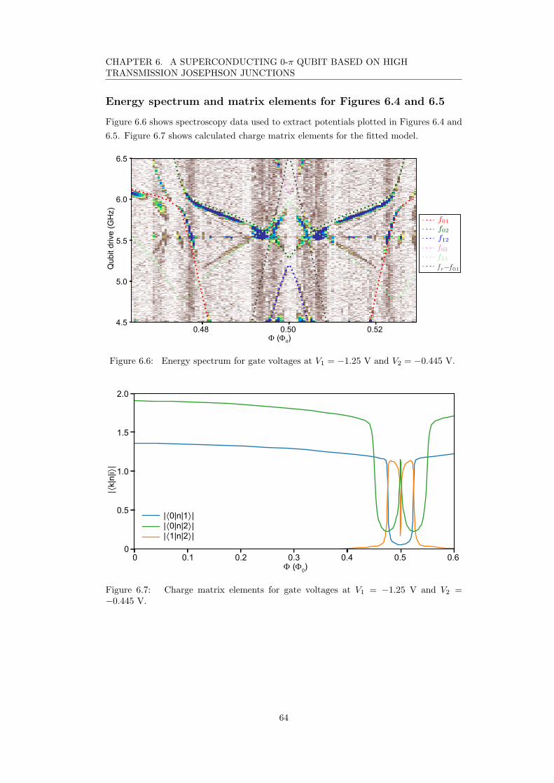
CHAPTER 6. A SUPERCONDUCTING 0-π QUBIT BASED ON HIGHTRANSMISSION JOSEPHSON JUNCTIONS
Energy spectrum and matrix elements for Figures 6.4 and 6.5
Figure 6.6 shows spectroscopy data used to extract potentials plotted in Figures 6.4 and
6.5. Figure 6.7 shows calculated charge matrix elements for the fitted model.
5.0
6.0
Qu
bit d
rive
(G
Hz)
6.5
5.5
4.5
Φ (Φ0)
0.500.48 0.52
Figure 6.6: Energy spectrum for gate voltages at V1 = −1.25 V and V2 = −0.445 V.
0 0.1 0.2 0.3 0.4 0.5 0.60
0.5
1.0
1.5
2.0
|〈k|n
|i〉|
|〈0|n|1〉||〈0|n|2〉||〈1|n|2〉|
Φ (Φ0)
Figure 6.7: Charge matrix elements for gate voltages at V1 = −1.25 V and V2 =−0.445 V.
64

Chapter 7
High field compatible
transmon circuit
Topological materials present an exciting direction to a scalable, topological quantum
computer [135, 136]. Recent studies have provided compelling evidence of Majorana
fermions in proximitized semiconducting nanowires with strong spin-orbit coupling [21,
22, 137, 138]. A controlled coupling of Majorana fermions, projecting the protected
qubit state into a measurable fermion parity, is a corner stone in several Majorana-based
qubits [136, 139]. A direct coupling of Majorana fermions on separate superconduc-
tors gives rise to a fractional Josephson effect. The fractional Josphson coupling might
be detected by embedding it into a well-known transmon circuit [140, 141], which pro-
vides well-established measurement techniques. In this Chapter we present a high-field
compatible transmon circuit, necessary to enter the topological phase, based on a sin-
gle superconductor-semiconductor nanowire capable of hosting Majorana fermions. We
show that the coherence of the transmon circuit is insensitive to low magnetic fields and
survives up to B = 1 T sufficient for Majorana fermions.
Transmon qubits exhibits harmonic oscillations in the superconducting phase differ-
ence between two superconductors with metastable, uncoupled parity states. Adding the
fractional Josephson effect of coupled Majorana fermions to the transmon allows dissi-
pationless, coherent transfer of single electrons coupling the odd and even parity sectors
of the transmon. The Hamiltonian of a transmon qubit with a Majorana coupling, a
Majorana transmon, is given by [140]:
H = 4EC(n− ng)2 − EJ cos(ϕ) + 2EM iγ2γ3 cos(ϕ/2), (7.1)
where EM is the coupling strength between Majorana fermions γ2 and γ3 with a super-
conducting phase difference ϕ. The product P = iγ2γ3 = ±1 is the fermion parity. Figure
7.1A shows the 4π-periodic potential of the Majorana transmon with EJ > EM and its
lowest energy states (not to scale for clarity). Inter-well transitions denoted A and C sepa-
rates by ±2EM from intra-well transitions denoted B due to the coupling of parity sectors
in the transmon circuit. For EJ ≫ EC the dispersion flattens out and EM is visible as a
65

CHAPTER 7. HIGH FIELD COMPATIBLE TRANSMON CIRCUIT
ϕ
2EM
B
BA
C
A B
Figure 7.1: A Potential of the Majorana transmon with EJ > EM . Lowest energy states(not to scale) are shown with the possible single-photon transitions. B Charge dispersionof transitions shown in A for EC/h = 400 MHz, EJ/EC = 27, EM/h = 0.5 MHz, andlinewidth k = 50 kHz. In the transmon limit EJ/EC ≫ 1 the dispersion flattens out andEM introduces a splitting between intra-well transitions B. B is adapted from [140].
splitting of intra-well transitions B due to a modification to the harmonic approximation
of each well from the fractional Josephson coupling: EJ cos(ϕ) ± EM cos(ϕ/2). In this
regime inter-well transitions A and C are suppressed due to non-overlapping wavefunc-
tions.
A topological nanowire with a small break in the aluminium shell as shown in Figure
7.2A is expected to host four Majorana fermions: one at each end and two on each side
of the junction. Large plunger electrodes, Vlplg and Vrplg, are used to tune the chemical
potential of the nanowire into a topological regime. With a third electrode, Vcut, at the
junction one can open or close the coupling between Majorana fermions γ2 and γ3. In
addition, as observed for gatemons, the junction will form a highly coherent Josephson
coupling allowing a single multichannel nanowire to mediate both the trivial Josephson
coupling as well as the topological Majorana coupling present in Equation (7.1). To turn
on the fractional Josephson effect we need to bring the system into a topological phase
by tuning chemical potential and magnetic field.
Figure 7.2B shows an InAs nanowire with diameter of ∼ 100 nm with one side covered
by a 7 nm thick aluminium shell. It is placed on NbTiN bottom gates using a micro
manipulator. A small part of the aluminium shell is etched away using a wet etch to
form a Josephson junction. The nanowire is connected to a T-shaped qubit island, with
simulated charging energy EC = 230 MHz, and the surrounding ground plane [Figure
7.2C]. A light RF mill is used to remove the native oxide of InAs before sputtering of
NbTiN contacts. The qubit island is capacitively coupled to λ/2 cavity with resonance
frequency ∼ 4.95 GHz for readout and microwave control. The cavity, qubit island, and
bottoms gates are fabricated for low loss and high-field compatibility in 20 nm NbTiN
[77, 142] using e-beam lithography and chlorine-based dry etch. A high density of flux
trapping holes is used to trap any flux vortices penetrating the thin NbTiN film. NbTiN
crossovers ties ground planes to avoid parasitic modes on the chip1. Local 5 nm HfO2
1It is crucial to not use aluminium on-chip bond wires to connect ground planes as these cause large
66

CHAPTER 7. HIGH FIELD COMPATIBLE TRANSMON CIRCUIT
CAB
VcutVlplg Vrplg
Island
B
Figure 7.2: A Device schematic. An InAs nanowire with one side covered in alu-minium (blue) is placed on top of plunger gates which tunes the chemical potential ofthe nanowire forming topological segments (green). A Majorana fermion forms at eachend the topological segments with an electrode Vcut controlling the coupling of γ2 and γ3as well as a trivial Josephson coupling EJ(Vcut). Schematic adapted from [144]. B Scan-ning electron micrograph of nanowire and bottom gates. C Micrograph of the transmonisland capacitively coupled to a λ/2 cavity for readout and microwave control.
deposited with ALD before the NbTiN deposition ensures no leakage between closely
spaced gates through the silicon substrate2. A second HfO2 layer 15 nm thick on top
of bottom gates acts as gate dielectric between bottom gates and nanowire. On chip
LC-filters (not shown) on each gate electrode suppress microwave dissipation through
the capacitively coupled gates [143]. A second qubit with no plunger gates is coupled to
the same resonator (not shown) but all data presented is from qubit shown. The sample
is placed inside a CuBe box filled with microwave absorbing Eccosorb foam to reduce
microwave and infrared radiation. The box is mounted in a dilution refrigerator with
base temperature < 50 mK (see Figure C.4 for schematic of setup).
7.1 Coherent Control up to 1 T
First we investigate the qubit behaviour in magnetic field parallel to the nanowire with
two-tone spectroscopy. During two-tone spectroscopy the cavity resonance is first mea-
sured for each magnetic field value to account for changes in the cavity resonance [See
Appendix Figure B.1]. Any out-of-plane magnetic field on order of 10 µT will modify
the resonance frequency of the cavity but we observe no degradation of resonator Q
factor or qubit lifetimes. Figure 7.3 shows the qubit frequency as a function of mag-
netic field up to 1 T. The qubit frequency exhibits a lobe structure with minima at
amount of dissipation above the critical field of aluminium.2Electrodes spaced ∼ 1 µm apart on bare, high-resistive silicon will leak at ∼ ±10 V at base
temperature.
67

CHAPTER 7. HIGH FIELD COMPATIBLE TRANSMON CIRCUIT
00.2
0.4
0.6
0.8
1B
(T)
2
2.5 3
3.5 4
Drive Frequency (GHz)
-40
040
Resonato
r response (a
u.)
Figure 7.3: Two-tone spectroscopy as a function of magnetic field. Changes in back-ground signal are due to adjustments to qubit drive power to account for varying lifetimeand detuning from resonator. Data around 0.58 T omitted due to a mistake in setupduring data acquisition. An average is subtracted from data at each magnetic field value.
68

CHAPTER 7. HIGH FIELD COMPATIBLE TRANSMON CIRCUIT
0 50 100 150 200t (ns)
0.0
0.2
0.4
0.6
0.8
1.0
No
rma
lize
d R
esp
on
se
(a
u.)
0 2 4 6 8 10 12 14Wait time (µs)
0.0
0.2
0.4
0.6
0.8
1.0
Norm
aliz
ed
Re
sp
on
se
(a
u.)
B = 0 T
B = 50 mT
B = 0 T
T1 = 5.5 µs
B = 50 mT
T1 = 5.0 µs
Figure 7.4: Upper (lower) panel shows Rabi oscillations (lifetime decay) of Majoranatransmon at 0 and 50 mT. The similarity in qubit performance highlights the Majoranatransmon’s resilience to magnetic fields. Data is normalized to extracted it parameters.
B ∼ 0.225 T and B ∼ 0.675 T. We interpret this as a suppression of the induced gap in
the semiconductor due to interference effects in the cross-section of the nanowire. The
current density in the semiconductor is mostly confined to the surface of the nanowire
forming a cylinder penetrated by a magnetic flux. At half-integer flux quanta through
the cylinder the superconductivity is suppressed due to destructive interference. This
agrees with resent simulations of the same nanowires [145]. We calculate the effective
diameter of the interference loop, assuming half a flux quantum at B = 0.225 T, to
be deff =√2Φ0/πB = 76 nm. As the current density resides inside the nanowire one
expects a slightly smaller effective diameter of the electron density than the ∼ 100 nm
diameter of the nanowire. Similar interference effects have recently been observed in
full-shell nanowire devices [146, 147].
The qubit behaviour can be split in the three lobes separated by the destructive
regimes. In the zeroth lobe measured from B ∼ 0 to ∼ 150 mT the device behaves indis-
tinguishably from a standard gatemon device. Due to the high drive power multiphoton
transitions are present displaying the higher energy states of the qubit. Around 150 mT
the system becomes unmeasurable due to the second qubit on the chip anticrossing with
the resonator [Figure B.1]. Figure 7.4 shows Rabi oscillations and lifetime decay at B = 0
and B = 50 mT. At B = 0 we observe lifetimes of ∼ 5.5 µs similar to previous gate-
mon devices verifying that additional plunger gates and dielectrics has not compromised
qubit performance. The measurements show almost no difference between B = 0 and
69

CHAPTER 7. HIGH FIELD COMPATIBLE TRANSMON CIRCUIT
0 50 100 150 200t (ns)
0.0
0.2
0.4
0.6
0.8
1.0
No
rma
lize
d R
esp
on
se
(a
u.)
0.0 0.2 0.4 0.6 0.8 1.0 1.2 1.4Wait time (µs)
0.0
0.2
0.4
0.6
0.8
1.0
Norm
aliz
ed
Re
sp
on
se
(a
u.) B = 1 T
T1 = 0.57 µs
B = 1 T
Figure 7.5: Upper (lower) panel shows Rabi osicllations (lifetime decay) of Majoranatransmon at B = 1 T.
B = 50 mT demonstrating excellent parallel magnetic field resilience consistent with
recent studies of gatemon qubits [113]. Furthermore, as the field is not finely aligned it
verifies that small out-of-plane magnetic fields do not degrade qubit quality. This might
eliminate the need for extensive magnetic shielding required in superconducting qubits.
Moving to higher fields in first lobe between ∼ 250 mT and ∼ 650 mT two main
resonances appear. Both states behaves as anharmonic oscillator modes with a broad
single-photon transition frequency and a sharper two-photon transition separated by
∼ 100 MHz. While the presence of two anharmonic states is consistent with a large EM
term in the Hamiltonian it is unlikely that the splitting is due to Majorana physics as
one expects higher magnetic fields to enter the topological phase. Rather the splitting
might be connected to low lying energy states coupling to the qubit mode. Indeed several
states dispersing strongly with magnetic fields are visible throughout the first lobe. It
was not possible to probe the qubit states in time domain due to very low lifetimes.
In the last lobe above B ∼ 650 mT a single qubit resonance revives with a clear two-
photon transition all the way up to B = 1 T. Figure 7.5 shows coherent Rabi oscillation
of a superconducting transmon qubit at B = 1 T with lifetime T1 = 0.57 µs strongly
encouraging the feasibility of the experimental setup for hosting Majorana fermions in a
coherent transmon. As in the first lobe other resonances strongly dispersing in magnetic
field are visible.
70

CHAPTER 7. HIGH FIELD COMPATIBLE TRANSMON CIRCUIT
7.2 Coupled Qubit and Junction states
To further investigate the anomalous qubit-resonance splitting we tune gate electrodes in
the first lobe into a regime with sharp transitions exhibiting qubit line splitting shown in
Figure 7.6. A clear, uninterrupted qubit transition frequency indicated by white dashed
line is slowly suppressed as the magnetic field is turned up. Additionally around the qubit
transition several new resonances appear above B = 350 mT oscillating as a function of
magnetic field. We speculate that these resonances might be explained by an Andreev
bound state indicated by the dashed purple line and a second state only weakly dependent
on magnetic field around energy f0 ∼ 6 GHz as indicated by the energy diagram inset
[Figure 7.6]. The blue and gray dashed lines are transitions from initially excited states
with frequencies f0 − fA and f0 − fqubit respectively. Purple and blue transitions appear
mirrored around f0/2 as their frequencies are given by f± = f0/2±δ where δ = fA−f0/2
(same for white and gray transitions).
At ∼ 360 mT an anticrossing appear between the qubit transition and the Andreev
transition f0 − fA (white and blue lines) indicating a strong coupling. Additionally,
the qubit resonance is also observed completely uncoupled from the Andreev transition.
The coexistence of the coupled and uncoupled spectra might be explained by the odd
and even parity of the Andreev state. In the even parity an Andreev state couples to
microwave excitation, such as the qubit resonance, while in the odd parity it is uncoupled
[148–150]. As the parity of the Andreev state is switching faster than the measurement
is performed we observed the average of the two cases: The odd case with a single qubit
resonance (white dashed line) uncoupled from the Andreev state, and the even case with
two transition frequencies from the avoided crossing of the qubit and Andreev transitions.
Combining the two cases we observe three resonances in the spectrum. Similarly when the
direct Andreev transition (purple line) is on resonance with the qubit near B ∼ 390 mT
three pronounced resonances are observed around the bare qubit frequency.
To further probe the spectrum in Figure 7.7 we sweep the gate voltage Vcut at fixed
magnetic fields. The strong dispersion of the Andreev state is a signature of a local
junction state strongly dependent on the electrostatics around the junction. Guides to
the eye indicate the same resonances as in Figure 7.6. As a function of gate voltage clear
anticrossings between the qubit resonance and both Andreev transitions are observed.
Also in gate voltage we observe a clear connection between the Andreev transitions given
by f± = f0/2±δ further evidence of the simple phenomenological model. At higher fields
more resonances appear complicating a full analysis of the spectrum. Further studies and
analysis are necessary to completely describe the multitude of transitions.
7.3 Conclusion
In conclusion we have presented simple gatemon circuit with excellent coherence times
of 5 µs at 50 mT. The qubit retains coherence up to magnetic fields of 1 T with life-
time T1 ∼ 0.6 µs demonstrating the feasibility of the circuit to coherently probe Ma-
jorana fermions. At high magnetic fields we observe several additional resonances in
71

CHAPTER 7. HIGH FIELD COMPATIBLE TRANSMON CIRCUIT
300 350 400 450 500B (mT)
2.6
2.8
3
3.2
3.4
3.6
3.8
Drive F
requency (
GH
z)
-2.0 -1.0 0 1.0Resonator response (au.)
fA
f0
fqubit
Figure 7.6: Spectroscopy reveals oscillating behaviour of junctions states at gate voltageVcut = −1.805 V and Vlplg = Vrplg = −1.983 V. Dashed lines are guides to the eye.Inset shows energy diagram of a phenomenological model consisting of a single stronglydispersing Andreev state fA and a non-dispersing state f0. An average is subtractedfrom each column.
-1.84 -1.82 -1.8 -1.78-1.84 -1.82 -1.8 -1.78
2.5
3
3.5
4
4.5
2.5
3
3.5
4
4.5
Drive
Fre
qu
en
cy (
GH
z)
Drive
Fre
qu
en
cy (
GH
z)
Vcut
(V) Vcut
(V)
B = 340 mT B = 350 mT
B = 360 mT B = 370 mT
Figure 7.7: Two-tone spectroscopy as a function of gate voltage Vcut for different mag-netic fields. Dashed lines are guides to the eye. Green dashed line is the resonance of thesecond qubit coupled to same resonator. An average is subtracted from each column.
72

CHAPTER 7. HIGH FIELD COMPATIBLE TRANSMON CIRCUIT
two-tone spectroscopy. We speculate that oscillating transitions present in the spectrum
are described by simple phenomenological model based on Andreev bound states in the
nanowire Josephson junction. Further studies with SQUID-type structures, allowing con-
trol of the superconducting phase across the Josephson junction, might help elucidating
the origin of these transitions by measuring their energy-phase relations. Alternatively
moving to systems with larger EC would allow distinguishing trivial junction states from
anharmonic oscillator modes by measuring charge dispersions, which carries the signature
of coupled Majorana fermions as shown in Figure 7.1. Additionally, high-field compatible
transmon qubits might open possibilities for hybrid systems such as spin ensemble-based
quantum memories in superconducting circuits [151].
73

Chapter 8
Outlook
It is an exciting time to work in experimental quantum computing research. During the
last decade both existing and emerging technologies for quantum bits have taken tremen-
dous steps towards true scalable quantum computing. The improvements are powered by
new architectures, scalable 2D ion-traps, new ideas, elimination of charge noise in trans-
mon qubits, and new materials, epitaxial semiconductor-superconductor interfaces. The
generally agreed upon strategy is to encode qubits in non-local, topological degrees of free-
dom decoupled from the environment. In this thesis we have investigated three different
approaches towards protected qubits all based on hybrid semiconductor-superconductor
nanowires. However, from the studies presented here, or in fact throughout the field of
experimental quantum computing, it is impossible to predict which platform will succeed.
In recent years most focus has been on superconducting qubits and quantum error
correction. These systems has the advantage of being able to optimize and benchmark
single qubits leading to amazing progress. We will likely see the first demonstration
of a small scale surface code outperforming its individual parts in the next few years.
However, going from small scale surface code to full fledged quantum computing is a
monumental task. Just the sheer number of qubits required is daunting. On top of
that comes a huge amount of classical computing power needed for error correction and
signal processing. Fortunately, no single challenge seems unsolvable and the rest might
”just” be engineering. One remaining essential question to be answered in quantum error
correction is: Are qubit errors truly local on large scale?
Topological materials or passive quantum error correction promise a different route
to quantum computing based on inherent protection. These platforms will also need a
form of active error correction to remove errors but the expected number of qubits is
much lower greatly reducing the challenge of scalability. The trade off is a complicated
materials or design problem to create a topological phase. As the topology is created by
the system itself it is very hard to prove that the system behaves as it should - any local
measurement cannot probe the topological degree of freedom we are interested in. The
main challenge is building the first qubit with control and readout both hard to achieve
due to the protected nature. Additionally the same question needs to be answered as
for quantum error correction: Are system errors truly topologically separated from the
74

CHAPTER 8. OUTLOOK
protected qubit?
Another tantalizing approach to scalable quantum computing are hybrid systems
containing both topological qubits and superconducting qubits. Each type of protection
might exhibit different advantages and disadvantages which can be utilized for different
parts of a quantum computer. For example superconducting qubits might be ideal for
magic state factories, which needs good initial T-gates, the T-gates performed without
protection, as well as fast gate operations for purification. However, as magic state
distillation is an inherent random procedure we want to store T-gates in quantum memory
until required for computation. Quantum memory requires long-lived qubits ideally with
low-overhead of classical computing power - maybe best implemented in low-overhead
topological materials. In this thesis we have demonstrated that the same architecture
might host different protected qubit. As topological qubits becomes a reality a research
direction lies in transferring quantum information from one type of protected qubit to
another to take full advantage each platform.
As mentioned it is an incredible exciting field to part of and I look forward to learn
about new ideas, inventions, and possibilities along the path to a quantum computer.
75

Appendices
76

Appendix A
Second order perturbation
theory
In this section we explicitly calculate the energy correction to second order in g/∆ for
the coupled circuit of transmon and resonator described in section 3.4. The generalized
Jaynes-Cummings Hamiltonian written with product eigenstates |n, j〉 of H0, where n is
the resonator excitation and j the atom excitation, is given by:
H = H0 + V , (A.1)
H0 = ~ωra†a+ ~
∑
i
ωi|i〉〈i|,
V = ~
∑
i
gi,i+1(a|i+ 1〉〈i|+ a†|i〉〈i+ 1|).
The correction to the eigenenergies can be found assuming gij = 0 for j 6= i ± 1. First
order correction is
E1|n,j〉 =〈n, j|V |n, j〉 = 0.
77
APPENDIX A. SECOND ORDER PERTURBATION THEORY
And second order:
E2|n,j〉
n,j>0=
∑
(m,i) 6=(n,j)
∣∣∣〈m, i|V |n, j〉∣∣∣2
E0|n,j〉 − E0
|m,i〉
=
∣∣∣〈n+ 1, j − 1|V |n, j〉∣∣∣2
E0|n,j〉 − E0
|n+1,j−1〉+
∣∣∣〈n− 1, j + 1|V |n, j〉∣∣∣2
E0|n,j〉 − E0
|n−1,j+1〉
=g2j−1,j(n+ 1)
~ωj − ~ωr+
g2j,j+1n
~ωr − ~ωj+1
=~χj−1,j(n+ 1)− ~χj,j+1n
E2|0,j〉
j>0=
∣∣∣〈1, j − 1|V |0, j〉∣∣∣2
E0|0,j〉 − E0
|1,j−1〉= ~χj−1,j
E2|n,0〉
n>0=
∣∣∣〈n− 1, 1|V |n, 0〉∣∣∣2
E0|n,0〉 − E0
|n−1,1〉= −~χ01n
E2|0,0〉 =0
where χij = g2ij/ωij − ωr. Collecting the terms the effective Hamiltonian becomes
Heff =∑
n,i
E|n,i〉|n, i〉〈n, i|
=~ωra†a+ ~
∑
i
ωi|i〉〈i|+ ~
∑
i
χi,i+1|i+ 1〉〈i+ 1|
− ~χ01a†a|0〉〈0|+ ~
∑
i=1
(χi−1,i − χi,i+1) a†a|i〉〈i|,
where the resonator states have been written with raising and lowering operators. Lastly
we truncate the transmon to a two-level system:
Heff =~ωra†a+ ~ω1|1〉〈1|+ ~χ01|1〉〈1|
− ~χ01a†a|0〉〈0|+ ~ (χ01 − χ12) a
†a|1〉〈1|=~(ωr − χ01|0〉〈0|+ (χ01 − χ12)|1〉〈1|)a†a+ ~(ω1 + χ01)|1〉〈1|
=~
(ωr −
χ12
2
)a†a+ ~
1
2(ω1 + χ01)σz + ~χa†aσz,
with χ = χ01 − χ12/2 and σz = |1〉〈1| − |0〉〈0|.
78

Appendix B
Magnetic field response of
NbTiN resonator
Figure B.1 shows resonator response measured interleaved with data in Figure 7.3 for
readout frequency adjustments.
0 0.2 0.4 0.6 0.8 1B magnitude (T)
4.91
4.92
4.93
4.94
4.95
4.96
Ca
vity F
req
ue
ncy (
GH
z)
S21 Magnitude (V)2 6 8 12
Figure B.1: Modulation of resonance frequency of the NbTiN, λ/2 cavity used forreadout in Chapter 7. Due to the large fluctuation the readout frequency is adjustedeach time the magnetic field is move. Large jumps around 0.2 T are due to correctionsof the out-of-plane magnetic field on order of ∼ 0.1 mT (not shown).
79

Appendix C
Schematics of Experimental
Setups
Schematics of each setup used for measurements presented in this thesis.
Aluminium box with indium seal used in setups presented in Figures C.1, C.2, and
C.3 is installed inside a copper box to reduce infrared radiation. The insides of both boxes
are covered in black absorptive paint (Aeroglaze Z306) to increase infrared absorption.
For setups C.2 and C.3 a long cylindrical cryoperm magnetic shield is installed.
The CuBe box in Figure C.4 is filled with non-magnetic Eccosorb foam (Eccosorb LS-
26) for dielectric absorption of radiation. As Aeroglaze Z306 is magnetically activated it
is unclear if it is effective at high magnetic fields required for the experiment.
80

APPENDIX C. SCHEMATICS OF EXPERIMENTAL SETUPS
Sample
Al box
Cu box
6d
B1
6d
B
ES
VL
FX
43
dB
<50mK
0.7K
4K
Quinstar isolator
CWJ1019-K414V
LF
X Minicircuits VLFX-300
ES ECCOSORB CR124
Cryogenic HEMT
Figure C.1: Schematic of setup for single qubit devices in Chapter 5. The data in Figure5.2 were acquired using a vector network analyzer. For the Sample 1 data in Figures5.3, 5.4, and 5.5 we mix down to dc and sample the homodyne response, VH . For theSample 2 data in Figure 5.5 we mix down to an intermediate frequency before samplingand then perform digital homodyne to extract the cavity phase response.
81

APPENDIX C. SCHEMATICS OF EXPERIMENTAL SETUPS
6
F
D
C
B
Sample
Al box
Cu box
20
dB
20
dB
<50mK
0.7K
89
7
5
3
21
4K
Minicircuits VLFX-300
low pass lter
QuinStar isolator
CWJ1019-K414
9
ECCOSORB CR124
low pass lter
8
DC Bias T7
6
RC low pass lter5
Marki Mixer
M8-0420MS
3
Midwest DC Block
DCB-3511
2
Picosecond Power Splitter
PSPL5333
1
Weinreb Cryogenic HEMT
Ampli er Cryo 1-12
Miteq Ampli erAFS3-00104200-35-ULN-R
Standford Reseach
Ampli er SR445A 5x
Agilent Vector Signal
Generator E8267C
D
F
C
B
A Rohde & Schwarz Vector
Signal Generator SGS100A
cryoperm
shield
20
dB
20
dB
Yokogawa
GS 200
A
A
A
Tektronix AWG 5014C
Trigger
RLI
I
I
I
Q
T
Alazar Card
Waveform digitizer
CH1 CH2 CH3 CH4
10dB
3d
B
6dB
HE
MT
16
dB
6d
B
3d
B
Miteq Ampli erAFS3-04000800-10-ULN-R
EE
3d
B
Rhode & Schwarz ZNB-20
Vector Network Analyser
M/C 4SPDT
RF switch
4
4
Figure C.2: Schematic of experimental setup for two qubit device in Chapter 5.
82

APPENDIX C. SCHEMATICS OF EXPERIMENTAL SETUPS
VLFX-300
Eccosorb
CR-124
Eccosorb
CR-110Drive Readout In Readout Out
<50 mK
0.7 K
4 K
Room temperature
Rhode & Swarchz
ZNB-8 4 port
Vector Network Analyzer
Textronix
5014C
Ch1
Ch2
Ch3
Ch4
M1
Yokogawa
GS200
MW switch
P1 P3 P2 P4
DC
V1,2
Flux
Isolator
Quinstar CWJ1019-K414
Bias T
C = 5.1 nF, R = 10 kΩ
Rhode & Swarchz
SGS100A
Mixer
Marki IQ0618LXP
Power splitter
A
B
B
K&L LP Filter
10GHz
B
Picosecond
35MHzA
Picosecond
DC block
40
dB
6 d
B6
dB
16
dB
20
dB
13
dB
20
dB
6 d
B3
dB
A
C C
B
3 dB
A
A
A
3 d
B
3 d
B
3 dB
3 dB
Alazar
ChA
ChB
Trg
A
B
Cryogenic Amplifier
CITCRYO1-12A
MITEQ
AFS3-00101200-35-ULN-R
C Standford Research
SR445A
Figure C.3: Schematic of experimental setup device in Chapter 6.
83
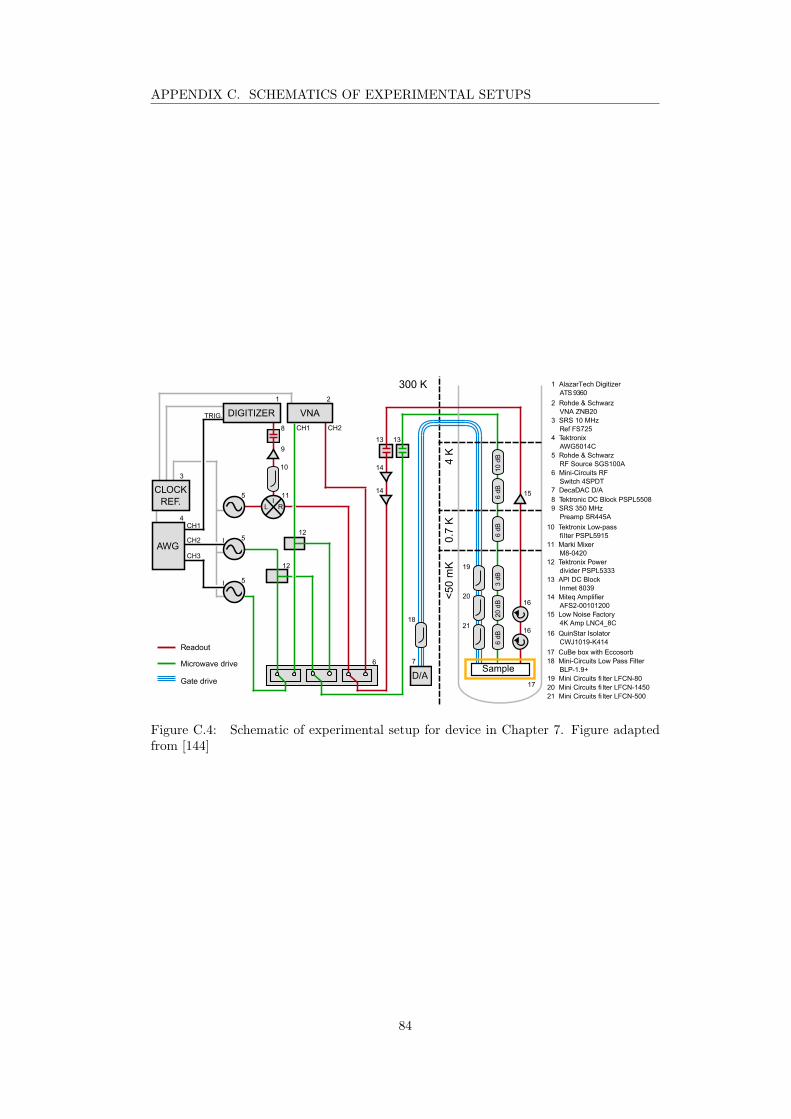
APPENDIX C. SCHEMATICS OF EXPERIMENTAL SETUPS
AWGI
Microwave drive
Readout
Gate drive
L RI
CH1
VNA
CH2
DIGITIZERTRIG.
CH1
CH2
CH3
I
D/A
6 d
B6 d
B10 d
B6 d
B20 d
B3 d
B
1 2
8
5 11
5
5
12
12
7
15
16
16
4
6
13
3
CLOCK
REF.
17
4 K
Sample
13
14
14
300 K 1 AlazarTech Digitizer
ATS 9360
9
10
18
2 Rohde & Schwarz
VNA ZNB20
3 SRS 10 MHz
Ref FS725
4 Tektronix
AWG5014C
5 Rohde & Schwarz
RF Source SGS100A
6 Mini-Circuits RF
Switch 4SPDT
7 DecaDAC D/A
8 Tektronic DC Block PSPL5508
9 SRS 350 MHz
Preamp SR445A
10 Tektronix Low-pass
fi lter PSPL5915
11 Marki Mixer
M8-0420
0.7
K<
50
mK 12 Tektronix Power
divider PSPL5333
13 API DC Block
Inmet 8039
14 Miteq Amplifier
AFS2-00101200
15 Low Noise Factory
4K Amp LNC4_8C
16 QuinStar Isolator
CWJ1019-K414
17 CuBe box with Eccosorb
19
20
21
19 Mini Circuits fi lter LFCN-80
20 Mini Circuits fi lter LFCN-1450
21 Mini Circuits fi lter LFCN-500
18 Mini-Circuits Low Pass Filter
BLP-1.9+
Figure C.4: Schematic of experimental setup for device in Chapter 7. Figure adaptedfrom [144]
84

Appendix D
Fabrication Recipes
Fabrication recipes for samples presented in this thesis. Metal evaporation and in situ
argon milling were done in an AJA International metal evaporation system. E-beamlithography were performed in a 100 kV Elionix electron beam lithography system.
D.1 Single qubit devices presented in Chapter 5
Al film deposition
• Silicon substrate with thermal oxide cleaned in acetone and IPA• Metal deposition: 1 min Ar mill, 75 nm Al
Gold alignment marks
• Resist spin: A4, 4000 rpm, 45 s, bake at 185C for 4 min• E-beam exposure: dose 1200 µC/cm2
• Development: 60 s MIBK:IPA 1:3, 10 s IPA, O2 plasma ash• Metal deposition: 10 nm Ti, 40 nm Au• Lift off: Acetone
Al film wet etching
• Resist spin: A4, 4000 rpm, 45 s, bake at 185C for 4 min• E-beam exposure: dose 1200 µC/cm2
• Development: 60 s MIBK:IPA 1:3, 10 s IPA, O2 plasma ash• Etch: 25 s Transene Type D at 54C, 30 s DI water, 10 s IPA• Resist strip: Acetone
Nanowire deposition
• Resist spin: A4, 4000 rpm, 45 s, bake at 185C for 4 min• E-beam exposure: dose 1200 µC/cm2
• Development: 60 s MIBK:IPA 1:3, 10 s IPA, O2 plasma ash• Nanowire dry deposition• Resist strip: Acetone
Gold alignment marks for nanowire
• Resist spin: A4, 4000 rpm, 45 s, bake at 185C for 4 min• E-beam exposure: dose 1200 µC/cm2
• Development: 60 s MIBK:IPA 1:3, 10 s IPA, O2 plasma ash• Metal deposition: 5 nm Ti, 35 nm Au• Lift off: Acetone
85

APPENDIX D. FABRICATION RECIPES
Nanowire wet etch
• Resist spin: A4, 4000 rpm, 45 s, bake at 185C for 4 min• E-beam exposure: dose 1200 µC/cm2
• Development: 60 s MIBK:IPA 1:3, 10 s IPA, O2 plasma ash• Etch: 12 s Transene Type D at 50C, 30 s DI water, 10 s IPA• Resist strip: Acetone
Nanowire contacts and side gate
• Resist spin: EL9, 4000 rpm, 45 s, bake at 185C for 1 min• Resist spin: A4, 4000 rpm, 45 s, bake at 185C for 4 min• E-beam exposure: dose 1200 µC/cm2
• Development: 60 s MIBK:IPA 1:3, 10 s IPA, O2 plasma ash• Metal deposition: 3 min Ar mill, 1 nm Ti, 150 nm Al• Resist strip: Acetone
D.2 Two-qubit device presented in Chapter 5
Al film deposition
• Silicon substrate with no thermal oxide cleaned in acetone and IPA• Metal deposition: 1 min Ar mill, 75 nm Al
Gold alignment marks
• Resist spin: A4, 4000 rpm, 45 s, bake at 185C for 3 min• E-beam exposure: dose 1200 µC/cm2
• Development: 60 s MIBK:IPA 1:3, 10 s IPA, O2 plasma ash• Metal deposition: 5 nm Ti, 45 nm Au• Lift off: Acetone
Al film wet etching
• Resist spin: EL9, 4000 rpm, 45 s, bake at 185C for 3 min• Resist spin: CSAR4, 4000 rpm, 45 s, bake at 185C for 3 min• E-beam exposure: dose 450 µC/cm2
• Development: 60 s O-xylene, 120 s MIBK:IPA 1:3, 15 s IPA, O2 plasma ash• Etch: 50 s Transene Type D at 53C, 30 s DI water, 15 s IPA (longer etch timedue to contaminated/old etch bottle)
• Resist strip: Acetone
Crossover oxide
• Resist spin: EL13, 4000 rpm, 45 s, bake at 185C for 3 min• Resist spin: CSAR4, 4000 rpm, 45 s, bake at 185C for 3 min• E-beam exposure: dose 450 µC/cm2
• Development: 60 s O-xylene, 120 s MIBK:IPA 1:3, 15 s IPA, O2 plasma ash• Oxide deposition: 250 nm SiO2• Lift off: Acetone
Crossover metal
• Resist spin: EL13, 4000 rpm, 45 s, bake at 185C for 3 min• Resist spin: CSAR4, 4000 rpm, 45 s, bake at 185C for 3 min• E-beam exposure: dose 450 µC/cm2
• Development: 60 s O-xylene, 120 s MIBK:IPA 1:3, 15 s IPA, O2 plasma ash• Metal deposition: 3 min Ar mill, 300 nm Al• Lift off: Acetone
86

APPENDIX D. FABRICATION RECIPES
Nanowire deposition
• Resist spin: EL9, 4000 rpm, 45 s, bake at 185C for 3 min• E-beam exposure: dose 450 µC/cm2
• Development: 60 s MIBK:IPA 1:3, 10 s IPA, O2 plasma ash• Nanowire dry deposition• Resist strip: Acetone
Nanowire wet etch
• Resist spin: A4, 4000 rpm, 45 s, bake at 185C for 4 min• E-beam exposure: dose 1200 µC/cm2
• Development: 60 s MIBK:IPA 1:3, 10 s IPA, O2 plasma ash• Etch: 12 s Transene Type D at 50C, 30 s DI water, 10 s IPA• Resist strip: Acetone
Gold alignment marks for nanowire
• Resist spin: A4, 4000 rpm, 45 s, bake at 185C for 3 min• E-beam exposure: dose 1200 µC/cm2
• Development: 60 s MIBK:IPA 1:3, 10 s IPA, O2 plasma ash• Metal deposition: 5 nm Ti, 45 nm Au• Lift off: Acetone
Nanowire contacts and side gate
• Resist spin: EL9, 4000 rpm, 45 s, bake at 185C for 1 min• Resist spin: A4, 4000 rpm, 45 s, bake at 185C for 4 min• E-beam exposure: dose 1200 µC/cm2
• Development: 60 s MIBK:IPA 1:3, 10 s IPA, O2 plasma ash• Metal deposition: 5.5 min Ar mill, 1 nm Ti, 150 nm Al• Resist strip: Acetone
Al film wet etching
• Resist spin: EL9, 4000 rpm, 45 s, bake at 185C for 3 min• Resist spin: CSAR4, 4000 rpm, 45 s, bake at 185C for 3 min• E-beam exposure: dose 450 µC/cm2
• Development: 60 s O-xylene, 120 s MIBK:IPA 1:3, 15 s IPA, O2 plasma ash• Etch: 20 s Transene Type D at 53C, 30 s DI water, 15 s IPA• Resist strip: Acetone
D.3 Device presented in Chapter 6
Deep etch silicon marks
• Resist spin: EL9, 4000 rpm, 45 s, bake at 185C for 1 min• Resist spin: CSAR9, 4000 rpm, 45 s, bake at 185C for 1 min• E-beam exposure: dose 400 µC/cm2
• Development: 60 s O-xylene, 75 s MIBK:IPA 1:3, 15 s IPA, O2 plasma ash• RIE deep etch: Gas cycles C4F8:SF6 1:1 / C4F8• Resist strip: O2 plasma
Al film and control etch
• Metal deposition: 1 min Ar mill, 100 nm Al• Resist spin: AZ1505, 4000 rpm, 45 s, bake at 115C for 2 min• UV exposure in a Heidelberg µPG101 LED writer: dose 20 ms• Development: 60 s AZdev:MQ 1:1, 30 s DI water, 30 s DI water, O2 plasma ash• Reactive Ion Etch: ICP 20 s Cl2, 15 s HBr:Cl2 3:5.• Resist strip: Acetone
87

APPENDIX D. FABRICATION RECIPES
SiOx crossover insulator
• Resist spin: LOR3B, 4000 rpm, 45 s, bake at 185C for 5 min• Resist spin: LOR3B, 4000 rpm, 45 s, bake at 185C for 5 min• Resist spin: AZ1505, 4000 rpm, 45 s, bake at 115C for 2 min• UV exposure in a Heidelberg µPG101 LED writer: dose 20 ms• Development: 60 s AZdev:MQ 1:1, 30 s DI water, 30 s DI water, O2 plasma ash• Oxide deposition: 200 nm SiO2• Resist strip: NMP
Bottom gates, these got damaged later due to fabrication mistake.
• Resist spin: EL9, 4000 rpm, 45 s, bake at 185C for 1 min• Resist spin: A4, 4000 rpm, 45 s, bake at 185C for 2 min• E-beam exposure: dose 1100 µC/cm2
• Development: 60 s MIBK:IPA 1:3, 10 s IPA, O2 plasma ash• Metal deposition: 30 nm Al• Resist strip: Acetone
Nanowire wet etch, bottom resist layers before nanowire placement meant to protectAl bottomgates from nanowire etch step. This failed leading to an etched bottom gatelikely due to a wrong dose in the e-beam exposure. Side gates were added to the designto compensate for the etched bottom gate.
• Resist spin: A4, 4000 rpm, 45 s, bake at 185C for 2 min• Resist spin: A4, 4000 rpm, 45 s, bake at 185C for 2 min• Nanowire placement with micromanipulator.• Resist spin: EL6:A4 2:3, 4000 rpm, 45 s, bake at 185C for 4 min• E-beam exposure: dose 500 µC/cm2
• Development: 60 s MIBK:IPA 1:3, 10 s IPA, O2 plasma ash• Etch: 9 s Transene Type D at 50C, 30 s DI water, 10 s IPA• Resist not stripped.
Nanowire contacts
• Resist spin: A4, 4000 rpm, 45 s, bake at 115C for 2 min• Resist spin: A4, 4000 rpm, 45 s, bake at 115C for 2 min• E-beam exposure: dose 1200 µC/cm2
• Development: 60 s MIBK:IPA 1:3, 10 s IPA, O2 plasma ash• Metal deposition: 5 min Ar mill, 1 nm Ti, 175 nm Al• Resist strip: Acetone
Nanowire sidegates
• Resist spin: A6, 4000 rpm, 45 s, bake at 115C for 2 min• Resist spin: A6, 4000 rpm, 45 s, bake at 115C for 2 min• E-beam exposure: dose 1200 µC/cm2
• Development: 60 s MIBK:IPA 1:3, 10 s IPA, O2 plasma ash• Metal deposition: 5 min Ar mill, 1 nm Ti, 175 nm Al• Resist strip: Acetone
D.4 Device presented in Chapter 7
Tungsten alignment marks
• Resist spin: LOR3B, 4000 rpm, 45 s, bake at 185C for 5 min• Resist spin: CSAR4, 4000 rpm, 45 s, bake at 115C for 2 min• E-beam exposure: dose 400 µC/cm2
• Development: 30 s ZED50, 20 s IPA, DI water rinse• Development: 5 s MF321, DI water rinse, O2 plasma ash• Metal deposition: 5 nm Ti, sputter ∼90 nm W• Lift off: NMP
88

APPENDIX D. FABRICATION RECIPES
Bottom ALD
• Resist spin: EL13, 4000 rpm, 45 s, bake at 185C for 1 min• Resist spin: A4, 4000 rpm, 45 s, bake at 185C for 1 min• E-beam exposure: dose 900 µC/cm2
• Development: 60 s MIBK:IPA 1:3, 15 s IPA, O2 plasma ash• ALD deposition: 5 nm HfOx at 90C• Lift off: NMP
NbTiN deposition and patterning
• Metal deposition: Sputter NbTi in N atmosphere 20 nm• Resist spin: CSAR9, 4000 rpm, 45 s, bake at 185C for 2 min• E-beam exposure: dose 400 µC/cm2
• Development: 60 s O-xylene, 15 s IPA, O2 plasma ash• Reactive Ion Etch: PRO ICP etcher with Cl2 gas• Resist strip: 1,3-dioxolane
Top ALD
• Resist spin: EL13, 4000 rpm, 45 s, bake at 185C for 1 min• Resist spin: A4, 4000 rpm, 45 s, bake at 185C for 1 min• E-beam exposure: dose 900 µC/cm2
• Development: 60 s MIBK:IPA 1:3, 15 s IPA, O2 plasma ash• ALD deposition: 15 nm HfOx at 90C• Lift off: NMP
Nanowire shell etch and NbTiN crossover insulator
• Resist spin: A4, 4000 rpm with slow acceleration, 45 s, bake at 115C for 2 min• E-beam exposure: dose 900 µC/cm2 for nanowire shell etch• E-beam exposure: dose 60 mC/cm2 for crosslinked PMMA insulator under NbTiNcrossovers
• Development: 60 s MIBK:IPA 1:3, 15 s IPA, O2 plasma ash• Etch: 9 s Transene Type D at 50C, 15 s DI water at 50C, 60 s DI water• Resist strip: Acetone
Nanowire contacts and NbTiN crossovers
• Resist spin: A4, 4000 rpm, 45 s, bake at 115C for 2 min• Resist spin: A4, 4000 rpm, 45 s, bake at 115C for 2 min• Resist spin: A4, 4000 rpm, 45 s, bake at 115C for 2 min• E-beam exposure: dose 900 µC/cm2 for nanowire shell etch• E-beam exposure: dose 60 mC/cm2 for crosslinked PMMA insulator under NbTiNcrossovers
• Development: 60 s MIBK:IPA 1:3, 10 s IPA, O2 plasma ash• Metal deposition: 5 min Ar mill, Sputter NbTi in N atmosphere 180 nm• Resist strip: 1,3-Dioxolane
89

Bibliography
[1] J. Bardeen & W.H.Brattain. “The transistor, a semiconductor triode”. Phys. Rev.
74.2, 230 (1948).
[2] W. Shockley. “Transistor technology evokes new physics”. Nobel lecture 344 (1956).
[3] J. S. Kilby. “Miniaturized electronic circuits”. US Patent 3,138,743 (1964).
[4] G. E. Moore. “Cramming more components onto integrated circuits”. Electronics
(1965).
[5] R. P. Feynman. “Simulating physics with computers”. International Journal of
Theoretical Physics 21, 467–488 (1982).
[6] S. Lloyd. “Universal Quantum Simulators”. Science 273, 1073–1078 (1996).
[7] D. S. Abrams & S. Lloyd. “Quantum Algorithm Providing Exponential Speed
Increase for Finding Eigenvalues and Eigenvectors”. Phys. Rev. Lett. 83, 5162–
5165 (1999).
[8] M. Schuld, I. Sinayskiy & F. Petruccione. “An introduction to quantum machine
learning”. Contemporary Physics 56, 172–185 (2015).
[9] L. K. Grover. “A fast quantum mechanical algorithm for database search”. In
the twenty-eighth annual ACM symposium, 212–219 (ACM Press, New York, New
York, USA, 1996).
[10] P. W. Shor. “Algorithms for Quantum Computation: Discrete Logarithms and
Factoring ”. In Proceedings 35th Annual Symposium on Foundations of Computer
Science, 124–134 (IEEE, 1994).
[11] T. P. Harty, D. T. C. Allcock, C. J. Ballance, L. Guidoni, H. A. Janacek, N. M.
Linke, D. N. Stacey & D. M. Lucas. “High-Fidelity Preparation, Gates, Memory,
and Readout of a Trapped-Ion Quantum Bit”. Phys. Rev. Lett. 113, 220501 (2014).
[12] T. Monz, D. Nigg, E. A. Martinez, M. F. Brandl, P. Schindler, R. Rines, S. X. Wang,
I. L. Chuang & R. Blatt. “Realization of a scalable Shor algorithm”. Science 351,
1068–1070 (2016).
90

BIBLIOGRAPHY
[13] C. Figgatt, D. Maslov, K. A. Landsman, N. M. Linke, S. Debnath & C. Monroe.
“Complete 3-Qubit Grover search on a programmable quantum computer”. Nature
Communications 8, 1918 (2017).
[14] R. J. Schoelkopf & S. M. Girvin. “Wiring up quantum systems.” Nature 451,
664–669 (2008).
[15] F. Yan, S. Gustavsson, A. Kamal, J. Birenbaum, A. P. Sears, D. Hover, T. J.
Gudmundsen, D. Rosenberg, G. Samach, S. Weber, J. L. Yoder, T. P. Orlando,
J. Clarke, A. J. Kerman & W. D. Oliver. “The flux qubit revisited to enhance
coherence and reproducibility”. Nature Communications 7, 1–9 (2016).
[16] N. Ofek, A. Petrenko, R. Heeres, P. Reinhold, Z. Leghtas, B. Vlastakis, Y. Liu, L.
Frunzio, S. M. Girvin, L. Jiang, M. Mirrahimi, M. H. Devoret & R. J. Schoelkopf.
“Extending the lifetime of a quantum bit with error correction in superconducting
circuits”. Nature 1–5 (2016).
[17] R. Barends, J. Kelly, A. Megrant, D. Sank, E. Jeffrey, Y. Chen, Y. Yin, B. Chiaro, J.
Mutus, C. Neill, P. O’Malley, P. Roushan, J. Wenner, T. C. White, A. N. Cleland &
J. M. Martinis. “Coherent Josephson qubit suitable for scalable quantum integrated
circuits.” Phys. Rev. Lett. 111, 080502 (2013).
[18] A. D. Corcoles, E. Magesan, S. J. Srinivasan, A. W. Cross, M. Steffen, J. M.
Gambetta & J. M. Chow. “Demonstration of a quantum error detection code
using a square lattice of four superconducting qubits.” Nature Communications 6,
6979 (2015).
[19] M. Veldhorst, J. C. C. Hwang, C. H. Yang, A. W. Leenstra, B. de Ronde, J. P.
Dehollain, J. T. Muhonen, F. E. Hudson, K. M. Itoh, A. Morello & A. S. Dzurak.
“An addressable quantum dot qubit with fault-tolerant control-fidelity”. Nature
Nanotechnology 9, 981 (2014).
[20] T. F. Watson, S. G. J. Philips, E. Kawakami, D. R. Ward, P. Scarlino, M. Veldhorst,
D. E. Savage, M. G. Lagally, M. Friesen, S. N. Coppersmith, M. A. Eriksson &
L. M. K. Vandersypen. “A programmable two-qubit quantum processor in silicon”.
Nature 555, 633 (2018).
[21] M. T. Deng, S. Vaitiekenas, E. B. Hansen, J. Danon, M. Leijnse, K. Flensberg,
J. Nygard, P. Krogstrup & C. M. Marcus. “Majorana bound state in a coupled
quantum-dot hybrid-nanowire system”. Science 354, 1557–1562 (2016).
[22] H. Zhang, C.-X. Liu, S. Gazibegovic, D. Xu, J. A. Logan, G. Wang, N. van Loo,
J. D. S. Bommer, M. W. A. de Moor, D. Car, R. L. M. Op het Veld, P. J. van Veld-
hoven, S. Koelling, M. A. Verheijen, M. Pendharkar, D. J. Pennachio, B. Shojaei,
J. S. Lee, C. J. Palmstrøm, E. P. A. M. Bakkers, S. D. Sarma & L. P. Kouwenhoven.
“Quantized Majorana conductance”. Nature 556, 74–79 (2018).
91

BIBLIOGRAPHY
[23] F. Nichele, A. C. C. Drachmann, A. M. Whiticar, E. C. T. O’Farrell, H. J. Suomi-
nen, A. Fornieri, T. Wang, G. C. Gardner, C. Thomas, A. T. Hatke, P. Krogstrup,
M. J. Manfra, K. Flensberg & C. M. Marcus. “Scaling of Majorana Zero-Bias
Conductance Peaks”. Phys. Rev. Lett. 119, 136803 (2017).
[24] Q. L. He, L. Pan, A. L. Stern, E. C. Burks, X. Che, G. Yin, J. Wang, B. Lian,
Q. Zhou, E. S. Choi, K. Murata, X. Kou, Z. Chen, T. Nie, Q. Shao, Y. Fan,
S.-C. Zhang, K. Liu, J. Xia & K. L. Wang. “Chiral Majorana fermion modes
in a quantum anomalous Hall insulator–superconductor structure”. Science 357,
294–299 (2017).
[25] D. Wang, L. Kong, P. Fan, H. Chen, S. Zhu, W. Liu, L. Cao, Y. Sun, S. Du, J.
Schneeloch, R. Zhong, G. Gu, L. Fu, H. Ding & H.-J. Gao. “Evidence for Majorana
bound states in an iron-based superconductor”. Science (2018).
[26] K. A. Y. Bravyi S B. “Quantum codes on a lattice with boundary”. arXiv:9811052
(1998).
[27] E. Knill. “Quantum computing with realistically noisy devices.” Nature 434, 39–44
(2005).
[28] H. Bombin & M. A. Martin-Delgado. “Topological Quantum Distillation”. Phys.
Rev. Lett. 97, 180501 (2006).
[29] B. Doucot & L. B. Ioffe. “Physical implementation of protected qubits”. Reports
on Progress in Physics 75, 072001 (2012).
[30] A. Y. Kitaev. “Unpaired Majorana fermions in quantum wires”. Phys. Usp. 44,
131–136 (2001).
[31] P. Krogstrup, N. L. B. Ziino, W. Chang, S. M. Albrecht, M. H. Madsen, E. John-
son, J. Nygard, C. M. Marcus & T. S. Jespersen. “Epitaxy of semiconductor–
superconductor nanowires”. Nature Materials 14, 400–406 (2015).
[32] R. Barends, J. Kelly, A. Megrant, A. Veitia, D. Sank, E. Jeffrey, T. C. White, J.
Mutus, A. G. Fowler, B. Campbell, Y. Chen, Z. Chen, B. Chiaro, A. Dunsworth, C.
Neill, P. O’Malley, P. Roushan, A. Vainsencher, J. Wenner, A. N. korotkov, A. N.
Cleland & J. M. Martinis. “Superconducting quantum circuits at the surface code
threshold for fault tolerance”. Nature 508, 500–503 (2014).
[33] J. Kelly, R. Barends, A. G. Fowler, A. Megrant, E. Jeffrey, T. C. White, D. Sank,
J. Y. Mutus, B. Campbell, Y. Chen, Z. Chen, B. Chiaro, A. Dunsworth, I. C. Hoi,
C. Neill, P. J. J. O’Malley, C. Quintana, P. Roushan, A. Vainsencher, J. Wenner,
A. N. Cleland & J. M. Martinis. “State preservation by repetitive error detection
in a superconducting quantum circuit”. Nature 519, 66–69 (2015).
[34] R. Versluis, S. Poletto, N. Khammassi, B. Tarasinski, N. Haider, D. J. Michalak,
A. Bruno, K. Bertels & L. DiCarlo. “Scalable Quantum Circuit and Control for a
Superconducting Surface Code”. Phys. Rev. Applied 8, 034021 (2017).
92

BIBLIOGRAPHY
[35] S. Gladchenko, D. Olaya, E. Dupont-Ferrier, B. Doucot, L. B. Ioffe & M. E. Ger-
shenson. “Superconducting nanocircuits for topologically protected qubits”. Nature
Physics 5, 48–53 (2009).
[36] M. T. Bell, J. Paramanandam, L. B. Ioffe & M. E. Gershenson. “Protected Joseph-
son Rhombus Chains”. Phys. Rev. Lett. 112, 167001 (2014).
[37] P. Groszkowski, A. D. Paolo, A. L. Grimsmo, A. Blais, D. I. Schuster, A. A. Houck
& J. Koch. “Coherence properties of the 0-π qubit”. New Journal of Physics 20,
043053 (2018).
[38] T. W. Larsen. Semiconductor-Nanowire-Based Superconducting Qubits and Gate-
Tunable Couplings. Master’s thesis, University of Copenhagen (2016).
[39] M. A. Nielsen & I. L. Chuang. Quantum Computation and Quantum Information.
10th Anniversary Edition (Cambridge University Press, Cambridge, 2009).
[40] D. P. DiVincenzo. “Two-bit gates are universal for quantum computation”. Phys.
Rev. A 51, 1015–1022 (1995).
[41] A. D. Corcoles, J. M. Gambetta, J. M. Chow, J. A. Smolin, M. Ware, J. Strand,
B. L. T. Plourde & M. Steffen. “Process verification of two-qubit quantum gates
by randomized benchmarking”. Phys. Rev. A 87, 030301 (2013).
[42] S. Pirandola, J. Eisert, C. Weedbrook, A. Furusawa & S. L. Braunstein. “Advances
in quantum teleportation”. Nature Photonics 9, 641 (2015).
[43] B. M. Terhal. “Quantum error correction for quantum memories”. Rev. Mod. Phys.
87, 307–346 (2015).
[44] D. Gottesman. Stabilizer Codes and Quantum Error Correction. Ph.D. thesis,
California Institute of Technology (1997).
[45] P. W. Shor. “Scheme for reducing decoherence in quantum computer memory”.
Phys. Rev. A 52, R2493–R2496 (1995).
[46] A. G. Fowler, M. Mariantoni, J. M. Martinis & A. N. Cleland. “Surface codes:
Towards practical large-scale quantum computation”. Phys. Rev. A 86, 032324
(2012).
[47] D. Poulin. “Optimal and efficient decoding of concatenated quantum block codes”.
Phys. Rev. A 74, 052333 (2006).
[48] A. S. Darmawan & D. Poulin. “Linear-time general decoding algorithm for the
surface code”. Phys. Rev. E 97, 051302 (2018).
[49] J. Alicea. “New directions in the pursuit of Majorana fermions in solid state
systems”. Reports on Progress in Physics 75, 076501 (2012).
93
BIBLIOGRAPHY
[50] R. M. Lutchyn, J. D. Sau & S. Das Sarma. “Majorana Fermions and a Topological
Phase Transition in Semiconductor-Superconductor Heterostructures”. Phys. Rev.
Lett. 105, 077001 (2010).
[51] Y. Oreg, G. Refael & F. von Oppen. “Helical Liquids and Majorana Bound States
in Quantum Wires”. Phys. Rev. Lett. 105, 177002 (2010).
[52] S. Bravyi & A. Kitaev. “Universal quantum computation with ideal Clifford gates
and noisy ancillas”. Phys. Rev. A 71, 022316 (2005).
[53] J. O’Gorman & E. T. Campbell. “Quantum computation with realistic magic-state
factories”. Phys. Rev. A 95, 032338 (2017).
[54] M. Reiher, N. Wiebe, K. M. Svore, D. Wecker & M. Troyer. “Elucidating reaction
mechanisms on quantum computers”. Proceedings of the National Academy of
Sciences 114, 7555–7560 (2017).
[55] J. T. Anderson, G. Duclos-Cianci & D. Poulin. “Fault-Tolerant Conversion between
the Steane and Reed-Muller Quantum Codes”. Phys. Rev. Lett. 113, 080501 (2014).
[56] H. Bombn. “Gauge color codes: optimal transversal gates and gauge fixing in
topological stabilizer codes”. New Journal of Physics 17, 083002 (2015).
[57] A. Blais, R.-S. Huang, A. Wallraff, S. M. Girvin & R. J. Schoelkopf. “Cavity
quantum electrodynamics for superconducting electrical circuits: An architecture
for quantum computation”. Phys. Rev. A 69, 062320 (2004).
[58] S. M. Girvin. “Circuit QED: Superconducting Qubits Coupled to Microwave Pho-
tons”. Oxford University Press (2011).
[59] U. Vool & M. Devoret. “Introduction to quantum electromagnetic circuits”. Inter-
national Journal of Circuit Theory and Applications 45, 897–934 (2017).
[60] B. Vlastakis, G. Kirchmair, Z. Leghtas, S. E. Nigg, L. Frunzio, S. M. Girvin,
M. Mirrahimi, M. H. Devoret & R. J. Schoelkopf. “Deterministically encoding
quantum information using 100-photon Schrodinger cat states.” Science 342, 607–
610 (2013).
[61] M. Mirrahimi, Z. Leghtas, V. V. Albert, S. Touzard, R. J. Schoelkopf, L. Jiang &
M. H. Devoret. “Dynamically protected cat-qubits: a new paradigm for universal
quantum computation”. New Journal of Physics 16, 045014 (2014).
[62] B. D. Josephson. “Possible new effects in superconductive tunnelling”. Phys. Lett.
1, 251–253 (1962).
[63] M. Tinkham. “Introduction to Superconductivity”. Dover Publications (1996).
[64] Y. Nakamura, Y. A. Pashkin & J. S. Tsai. “Coherent control of macroscopic
quantum states in a single-Cooper-pair box”. Nature 398, 786 (1999).
94

BIBLIOGRAPHY
[65] D. Vion, A. Aassime, A. Cottet, P. Joyez, H. Pothier, C. Urbina, D. Esteve & M. H.
Devoret. “Manipulating the Quantum State of an Electrical Circuit”. Science 296,
886–889 (2002).
[66] A. Wallraff, D. I. Schuster, A. Blais, L. Frunzio, R.-S. Huang, J. Majer, S. Kumar,
S. M. Girvin & R. J. Schoelkopf. “Strong coupling of a single photon to a super-
conducting qubit using circuit quantum electrodynamics.” Nature 431, 162–167
(2004).
[67] J. Koch, T. Yu, J. Gambetta, A. Houck, D. Schuster, J. Majer, A. Blais, M.
Devoret, S. Girvin & R. Schoelkopf. “Charge-insensitive qubit design derived from
the Cooper pair box”. Phys. Rev. A 76, 042319 (2007).
[68] J. Schreier, A. Houck, J. Koch, D. Schuster, B. Johnson, J. Chow, J. Gambetta,
J. Majer, L. Frunzio, M. Devoret, S. Girvin & R. Schoelkopf. “Suppressing charge
noise decoherence in superconducting charge qubits”. Phys. Rev. B 77, 180502
(2008).
[69] J. M. Chow, J. M. Gambetta, L. Tornberg, J. Koch, L. S. Bishop, A. A. Houck,
B. R. Johnson, L. Frunzio, S. M. Girvin & R. J. Schoelkopf. “Randomized Bench-
marking and Process Tomography for Gate Errors in a Solid-State Qubit”. Phys.
Rev. Lett. 102, 090502 (2009).
[70] F. Motzoi, J. M. Gambetta, P. Rebentrost & F. K. Wilhelm. “Simple Pulses for
Elimination of Leakage in Weakly Nonlinear Qubits”. Phys. Rev. Lett. 103, 110501
(2009).
[71] J. M. Gambetta, F. Motzoi, S. T. Merkel & F. K. Wilhelm. “Analytic control
methods for high-fidelity unitary operations in a weakly nonlinear oscillator”. Phys.
Rev. A 83, 012308 (2011).
[72] M. Kjaergaard, F. Nichele, H. J. Suominen, M. P. Nowak, M. Wimmer, A. R.
Akhmerov, J. A. Folk, K. Flensberg, J. Shabani, C. J. Palmstrm & C. M. Marcus.
“Quantized conductance doubling and hard gap in a two-dimensional semiconduc-
torsuperconductor heterostructure”. Nature Communications 7, 012308 (2016).
[73] T. W. Larsen, K. D. Petersson, F. Kuemmeth, T. S. Jespersen, P. Krogstrup,
J. Nygard & C. M. Marcus. “Semiconductor-Nanowire-Based Superconducting
Qubit”. Phys. Rev. Lett. 115, 127001 (2015).
[74] G. de Lange, B. van Heck, A. Bruno, D. J. van Woerkom, A. Geresdi, S. R.
Plissard, E. P. A. M. Bakkers, A. R. Akhmerov & L. DiCarlo. “Realization
of Microwave Quantum Circuits Using Hybrid Superconducting-Semiconducting
Nanowire Josephson Elements”. Phys. Rev. Lett. 115, 127002 (2015).
[75] J. I.-J. Wang, D. Rodan-Legrain, L. Bretheau, D. L. Campbell, B. Kannan, D. Kim,
M. Kjaergaard, P. Krantz, G. O. Samach, F. Yan, J. L. Yoder, K. Watanabe, T.
95

BIBLIOGRAPHY
Taniguchi, T. P. Orlando, S. Gustavsson, P. Jarillo-Herrero &W. D. Oliver. “Quan-
tum coherent control of a hybrid superconducting circuit made with graphene-based
van der Waals heterostructures”. arXiv:1809.05215 (2018).
[76] L. Casparis, M. R. Connolly, M. Kjaergaard, N. J. Pearson, A. K. j, T. W. Larsen,
F. Kuemmeth, T. Wang, C. Thomas, S. Gronin, G. C. Gardner, M. J. Manfra,
C. M. Marcus & K. D. Petersson. “Superconducting gatemon qubit based on a
proximitized two-dimensional electron gas”. Nature Nanotechnology 13, 915 (2018).
[77] J. G. Kroll, W. Uilhoorn, K. L. van der Enden, D. de Jong, K. Watanabe, T.
Taniguchi, S. Goswami, M. C. Cassidy & L. P. Kouwenhoven. “A graphene trans-
mon operating at 1 T”. arXiv:1806.10534 (2018).
[78] W. Chang, S. M. Albrecht, T. S. Jespersen, F. Kuemmeth, P. Krogstrup, J.
Nygard & C. M. Marcus. “Hard gap in epitaxial semiconductor–superconductor
nanowires”. Nature Nanotechnology 10, 232–236 (2015).
[79] S. Chuang, Q. Gao, R. Kapadia, A. C. Ford, J. Guo & A. Javey. “Ballistic InAs
Nanowire Transistors”. Nano Letters 13, 555–558 (2013).
[80] A. Kringhøj, L. Casparis, M. Hell, T. W. Larsen, F. Kuemmeth, M. Leijnse, K.
Flensberg, P. Krogstrup, J. Nygard, K. D. Petersson & C. M. Marcus. “Anhar-
monicity of a superconducting qubit with a few-mode Josephson junction”. Phys.
Rev. B 97, 060508 (2018).
[81] C. W. J. Beenakker. “Universal limit of critical-current fluctuations in mesoscopic
Josephson junctions”. Phys. Rev. Lett. 67, 3836–3839 (1991).
[82] A. A. Golubov, M. Y. Kupriyanov & E. Il’ichev. “The current-phase relation in
Josephson junctions”. Rev. Mod. Phys. 76, 411–469 (2004).
[83] M. F. Goffman, C. Urbina, H. Pothier, J. Nygrd, C. M. Marcus & P. Krogstrup.
“Conduction channels of an InAs-Al nanowire Josephson weak link”. New Journal
of Physics 19, 092002 (2017).
[84] E. M. Spanton, M. Deng, S. Vaitieknas, P. Krogstrup, J. Nygrd, C. M. Marcus
& K. A. Moler. “Currentphase relations of few-mode InAs nanowire Josephson
junctions”. Nature Physics 13, 1177 (2017).
[85] D. J. van Woerkom, A. Proutski, B. van Heck, D. Bouman, J. I. Vyrynen, L. I.
Glazman, P. Krogstrup, J. Nygrd, L. P. Kouwenhoven & A. Geresdi. “Microwave
spectroscopy of spinful Andreev bound states in ballistic semiconductor Josephson
junctions”. Nature Physics 13, 876 (2017).
[86] D. V. Averin. “Coulomb blockade in superconducting quantum point contacts”.
Phys. Rev. Lett. 82, 3685 (1999).
[87] A. Wallraff, D. I. Schuster, A. Blais, L. Frunzio, J. Majer, M. H. Devoret, S. M.
Girvin & R. J. Schoelkopf. “Approaching Unit Visibility for Control of a Super-
conducting Qubit with Dispersive Readout”. Phys. Rev. Lett. 95, 060501 (2005).
96

BIBLIOGRAPHY
[88] A. Houck, J. Schreier, B. Johnson, J. Chow, J. Koch, J. Gambetta, D. Schuster,
L. Frunzio, M. Devoret, S. Girvin & R. Schoelkopf. “Controlling the Spontaneous
Emission of a Superconducting Transmon Qubit”. Phys. Rev. Lett. 101, 080502
(2008).
[89] D. I. Schuster, A. Wallraff, A. Blais, L. Frunzio, R.-S. Huang, J. Majer, S. M.
Girvin & R. J. Schoelkopf. “ac Stark Shift and Dephasing of a Superconducting
Qubit Strongly Coupled to a Cavity Field”. Phys. Rev. Lett. 94, 123602 (2005).
[90] D. I. Schuster, A. A. Houck, J. A. Schreier, A. Wallraff, J. M. Gambetta, A. Blais,
L. Frunzio, J. Majer, B. Johnson, M. H. Devoret, S. M. Girvin & R. J. Schoelkopf.
“Resolving photon number states in a superconducting circuit”. Nature 445, 515–
518 (2007).
[91] D. Riste, C. C. Bultink, K. W. Lehnert & L. DiCarlo. “Feedback Control of a
Solid-State Qubit Using High-Fidelity Projective Measurement”. Phys. Rev. Lett.
109, 240502 (2012).
[92] Y. Salathe, P. Kurpiers, T. Karg, C. Lang, C. K. Andersen, A. Akin, S. Krinner,
C. Eichler & A. Wallraff. “Low-Latency Digital Signal Processing for Feedback and
Feedforward in Quantum Computing and Communication”. Phys. Rev. Applied 9,
034011 (2018).
[93] E. M. Purcell, H. C. Torrey & R. V. Pound. “Resonance Absorption by Nuclear
Magnetic Moments in a Solid”. Phys. Rev. 69, 37–38 (1946).
[94] M. D. Reed, B. R. Johnson, A. A. Houck, L. DiCarlo, J. M. Chow, D. I. Schuster,
L. Frunzio & R. J. Schoelkopf. “Fast reset and suppressing spontaneous emission
of a superconducting qubit”. Applied Physics Letters 96, 203110 (2010).
[95] E. Jeffrey, D. Sank, J. Y. Mutus, T. C. White, J. Kelly, R. Barends, Y. Chen,
Z. Chen, B. Chiaro, A. Dunsworth, A. Megrant, P. J. J. O’Malley, C. Neill, P.
Roushan, A. Vainsencher, J. Wenner, A. N. Cleland & J. M. Martinis. “Fast
Accurate State Measurement with Superconducting Qubits”. Phys. Rev. Lett. 112,
190504 (2014).
[96] E. A. Sete, J. M. Martinis & A. N. Korotkov. “Quantum theory of a bandpass
Purcell filter for qubit readout”. Phys. Rev. A 92, 012325 (2015).
[97] N. T. Bronn, E. Magesan, N. A. Masluk, J. M. Chow, J. M. Gambetta & M. Stef-
fen. “Reducing Spontaneous Emission in Circuit Quantum Electrodynamics by a
Combined Readout/Filter Technique”. IEEE Transactions on Applied Supercon-
ductivity 25, 1–10 (2015).
[98] J. M. Chow, A. D. Corcoles, J. M. Gambetta, C. Rigetti, B. R. Johnson, J. A.
Smolin, J. R. Rozen, G. A. Keefe, M. B. Rothwell, M. B. Ketchen & M. Stef-
fen. “Simple All-Microwave Entangling Gate for Fixed-Frequency Superconducting
Qubits”. Phys. Rev. Lett. 107, 080502 (2011).
97

BIBLIOGRAPHY
[99] Y. Chen, C. Neill, P. Roushan, N. Leung, M. Fang, R. Barends, J. Kelly, B. Camp-
bell, Z. Chen, B. Chiaro, A. Dunsworth, E. Jeffrey, A. Megrant, J. Y. Mutus,
P. J. J. O’Malley, C. M. Quintana, D. Sank, A. Vainsencher, J. Wenner, T. C.
White, M. R. Geller, A. N. Cleland & J. M. Martinis. “Qubit Architecture with
High Coherence and Fast Tunable Coupling”. Phys. Rev. Lett. 113, 220502 (2014).
[100] N. J. S. Loft, M. Kjaergaard, L. B. Kristensen, C. K. Andersen, T. W. Larsen,
S. Gustavsson, W. D. Oliver & N. T. Zinner. “High-fidelity conditional two-qubit
swapping gate using tunable ancillas”. arxiv:1809.09049 (2018).
[101] F. Yan, P. Krantz, Y. Sung, M. Kjaergaard, D. Campbell, J. I. Wang, T. P. Orlando,
S. Gustavsson & W. D. Oliver. “A tunable coupling scheme for implementing high-
fidelity two-qubit gates”. arXiv:1803.09813 (2018).
[102] L. DiCarlo, J. M. Chow, J. M. Gambetta, L. S. Bishop, B. R. Johnson, D. I. Schus-
ter, J. Majer, A. Blais, L. Frunzio, S. M. Girvin & R. J. Schoelkopf. “Demonstration
of two-qubit algorithms with a superconducting quantum processor”. Nature 460,
240–244 (2009).
[103] J. M. Martinis & M. R. Geller. “Fast adiabatic qubit gates using only σz control”.
Phys. Rev. A 90, 022307 (2014).
[104] A. Dewes, F. R. Ong, V. Schmitt, R. Lauro, N. Boulant, P. Bertet, D. Vion & D.
Esteve. “Characterization of a Two-Transmon Processor with Individual Single-
Shot Qubit Readout”. Phys. Rev. Lett. 108, 057002 (2012).
[105] J. Majer, J. M. Chow, J. M. Gambetta, J. Koch, B. R. Johnson, J. A. Schreier, L.
Frunzio, D. I. Schuster, A. A. Houck, A. Wallraff, A. Blais, M. H. Devoret, S. M.
Girvin & R. J. Schoelkopf. “Coupling superconducting qubits via a cavity bus”.
Nature 449, 443–447 (2007).
[106] M. Reed. Entanglement and Quantum Error Correction with Superconducting
Qubits. Ph.D. thesis, Yale University (2013).
[107] T. Tanamoto, K. Maruyama, Y.-x. Liu, X. Hu & F. Nori. “Efficient purification
protocols using iSWAP gates in solid-state qubits”. Phys. Rev. A 78, 062313 (2008).
[108] J. Kelly, R. Barends, B. Campbell, Y. Chen, Z. Chen, B. Chiaro, A. Dunsworth,
A. G. Fowler, I. C. Hoi, E. Jeffrey, A. Megrant, J. Mutus, C. Neill, P. J. J. O’Malley,
C. Quintana, P. Roushan, D. Sank, A. Vainsencher, J. Wenner, T. C. White,
A. N. Cleland & J. M. Martinis. “Optimal Quantum Control Using Randomized
Benchmarking”. Phys. Rev. Lett. 112, 240504 (2014).
[109] A. Megrant, C. Neill, R. Barends, B. Chiaro, Y. Chen, L. Feigl, J. Kelly, E. Lucero,
M. Mariantoni, P. J. J. OMalley, D. Sank, A. Vainsencher, J. Wenner, T. C. White,
Y. Yin, J. Zhao, C. J. Palmstrm, J. M. Martinis & A. N. Cleland. “Planar su-
perconducting resonators with internal quality factors above one million”. Applied
Physics Letters 100, 113510 (2012).
98

BIBLIOGRAPHY
[110] Z. Chen, A. Megrant, J. Kelly, R. Barends, J. Bochmann, Y. Chen, B. Chiaro,
A. Dunsworth, E. Jeffrey, J. Y. Mutus, P. J. J. O’Malley, C. Neill, P. Roushan,
D. Sank, A. Vainsencher, J. Wenner, T. C. White, A. N. Cleland & J. M. Marti-
nis. “Fabrication and characterization of aluminum airbridges for superconducting
microwave circuits”. Applied Physics Letters 104, 052602 (2014).
[111] A. Bruno, G. de Lange, S. Asaad, K. L. van der Enden, N. K. Langford & L.
DiCarlo. “Reducing intrinsic loss in superconducting resonators by surface treat-
ment and deep etching of silicon substrates”. Applied Physics Letters 106, 182601
(2015).
[112] C. Wang, C. Axline, Y. Y. Gao, T. Brecht, Y. Chu, L. Frunzio, M. H. Devoret
& R. J. Schoelkopf. “Surface participation and dielectric loss in superconducting
qubits”. Applied Physics Letters 107, 162601 (2015).
[113] F. Luthi, T. Stavenga, O. W. Enzing, A. Bruno, C. Dickel, N. K. Langford, M. A.
Rol, T. S. Jespersen, J. Nygard, P. Krogstrup & L. DiCarlo. “Evolution of Nanowire
Transmon Qubits and Their Coherence in a Magnetic Field”. Phys. Rev. Lett. 120,
100502 (2018).
[114] W. Chang. Superconducting Proximity Effect in InAs Nanowires. Ph.D. thesis,
Harvard University (2014).
[115] A. D. Crcoles, J. M. Chow, J. M. Gambetta, C. Rigetti, J. R. Rozen, G. A. Keefe,
M. Beth Rothwell, M. B. Ketchen & M. Steffen. “Protecting superconducting
qubits from radiation”. Applied Physics Letters 99, 181906 (2011).
[116] R. Barends, J. Wenner, M. Lenander, Y. Chen, R. C. Bialczak, J. Kelly, E. Lucero,
P. OMalley, M. Mariantoni, D. Sank, H. Wang, T. C. White, Y. Yin, J. Zhao,
A. N. Cleland, J. M. Martinis & J. J. A. Baselmans. “Minimizing quasiparticle
generation from stray infrared light in superconducting quantum circuits”. Applied
Physics Letters 99, 113507 (2011).
[117] D. Schuster. Circuit Quantum Electrodynamics. Ph.D. thesis, Yale University
(2007).
[118] L. Casparis, T. W. Larsen, M. S. Olsen, F. Kuemmeth, P. Krogstrup, J. Nygard,
K. D. Petersson & C. M. Marcus. “Gatemon Benchmarking and Two-Qubit Op-
erations”. Phys. Rev. Lett. 116, 150505 (2016).
[119] A. A. AU Houck, D. I. Schuster, J. M. Gambetta, J. A. Schreier, B. R. Johnson,
J. M. Chow, L. Frunzio, J. Majer, M. H. Devoret, S. M. Girvin & R. J. Schoelkopf.
“Generating single microwave photons in a circuit”. Nature 449, 328 (2007).
[120] u. Cywinski. “Dynamical-decoupling noise spectroscopy at an optimal working
point of a qubit”. Phys. Rev. A 90, 042307 (2014).
99

BIBLIOGRAPHY
[121] I. L. Chuang & M. A. Nielsen. “Prescription for experimental determination of
the dynamics of a quantum black box”. Journal of Modern Optics 44, 2455–2467
(1997).
[122] R. Bhandari & N. A. Peters. “On the general constraints in single qubit quantum
process tomography”. Scientific Reports 6, 26004 (2016).
[123] E. Magesan, J. M. Gambetta, B. R. Johnson, C. A. Ryan, J. M. Chow, S. T.
Merkel, M. P. da Silva, G. A. Keefe, M. B. Rothwell, T. A. Ohki, M. B. Ketchen
& M. Steffen. “Efficient Measurement of Quantum Gate Error by Interleaved
Randomized Benchmarking”. Phys. Rev. Lett. 109, 080505 (2012).
[124] P. J. J. O’Malley, J. Kelly, R. Barends, B. Campbell, Y. Chen, Z. Chen, B. Chiaro,
A. Dunsworth, A. G. Fowler, I.-C. Hoi, E. Jeffrey, A. Megrant, J. Mutus, C. Neill,
C. Quintana, P. Roushan, D. Sank, A. Vainsencher, J. Wenner, T. C. White, A. N.
Korotkov, A. N. Cleland & J. M. Martinis. “Qubit Metrology of Ultralow Phase
Noise Using Randomized Benchmarking”. Phys. Rev. Applied 3, 044009 (2015).
[125] L. Casparis, N. J. Pearson, A. K. j, T. W. Larsen, F. Kuemmeth, J. N. rd, P.
Krogstrup, K. D. Petersson & C. M. Marcus. “Voltage-Controlled Superconducting
Quantum Bus”. arXiv:1802.01327 (2018).
[126] A. Kitaev. “Protected qubit based on a superconducting current mirror”.
arXiv:0609441 (2006).
[127] P. Brooks, A. Kitaev & J. Preskill. “Protected gates for superconducting qubits”.
Phys. Rev. A 87, 052306 (2013).
[128] B. Doucot & J. Vidal. “Pairing of Cooper Pairs in a Fully Frustrated Josephson-
Junction Chain”. Phys. Rev. Lett. 88, 227005 (2002).
[129] C. W. J. Beenakker & H. van Houten. “The Superconducting Quantum Point
Contact”. 481–497 (Elsevier, 1992).
[130] Y.-H. Lin, L. B. Nguyen, N. Grabon, J. San Miguel, N. Pankratova & V. E.
Manucharyan. “Demonstration of Protection of a Superconducting Qubit from
Energy Decay”. Phys. Rev. Lett. 120, 150503 (2018).
[131] N. Earnest, S. Chakram, Y. Lu, N. Irons, R. K. Naik, N. Leung, L. Ocola, D. A.
Czaplewski, B. Baker, J. Lawrence, J. Koch & D. I. Schuster. “Realization of a Λ
System with Metastable States of a Capacitively Shunted Fluxonium”. Phys. Rev.
Lett. 120, 150504 (2018).
[132] A. E. Antipov, A. Bargerbos, G. W. Winkler, B. Bauer, E. Rossi & R. M. Lutchyn.
“Effects of Gate-Induced Electric Fields on Semiconductor Majorana Nanowires”.
Phys. Rev. X 8, 031041 (2018).
[133] S. Vaitiekenas, M.-T. Deng, J. Nygard, P. Krogstrup & C. M. Marcus. “Effective
g Factor of Subgap States in Hybrid Nanowires”. Phys. Rev. Lett. 121, 037703
(2018).
100

BIBLIOGRAPHY
[134] N. Didier, J. Bourassa & A. Blais. “Fast Quantum Nondemolition Readout by
Parametric Modulation of Longitudinal Qubit-Oscillator Interaction”. Phys. Rev.
Lett. 115, 203601 (2015).
[135] T. Karzig, C. Knapp, R. M. Lutchyn, P. Bonderson, M. B. Hastings, C. Nayak,
J. Alicea, K. Flensberg, S. Plugge, Y. Oreg, C. M. Marcus & M. H. Freedman.
“Scalable designs for quasiparticle-poisoning-protected topological quantum com-
putation with Majorana zero modes”. Phys. Rev. B 95, 235305 (2017).
[136] S. Plugge, A. Rasmussen, R. Egger & K. Flensberg. “Majorana box qubits”. New
Journal of Physics 19, 012001 (2017).
[137] V. Mourik, K. Zuo, S. M. Frolov, S. R. Plissard, E. P. A. M. Bakkers & L. P.
Kouwenhoven. “Signatures of Majorana Fermions in Hybrid Superconductor-
Semiconductor Nanowire Devices”. Science 336, 1003–1007 (2012).
[138] S. M. Albrecht, A. P. Higginbotham, M. Madsen, F. Kuemmeth, T. S. Jespersen,
J. Nygard, P. Krogstrup & C. M. Marcus. “Exponential protection of zero modes
in Majorana islands”. Nature 531, 206–209 (2016).
[139] D. Aasen, M. Hell, R. V. Mishmash, A. Higginbotham, J. Danon, M. Leijnse, T. S.
Jespersen, J. A. Folk, C. M. Marcus, K. Flensberg & J. Alicea. “Milestones Toward
Majorana-Based Quantum Computing”. Phys. Rev. X 6, 031016 (2016).
[140] E. Ginossar & E. Grosfeld. “Microwave transitions as a signature of coherent parity
mixing effects in the Majorana-transmon qubit”. Nature Communications 5, 4772
(2014).
[141] K. Yavilberg, E. Ginossar & E. Grosfeld. “Fermion parity measurement and control
in Majorana circuit quantum electrodynamics”. Phys. Rev. B 92, 075143 (2015).
[142] J. G. Kroll, F. Borsoi, K. L. van der Enden, W. Uilhoorn, D. de Jong, M. Quintero-
Prez, D. J. van Woerkom, A. Bruno, S. R. Plissard, D. Car, E. P. A. M. Bakkers,
M. C. Cassidy & L. P. Kouwenhoven. “Magnetic field resilient superconducting
coplanar waveguide resonators for hybrid cQED experiments”. arXiv:1809.03932
(2018).
[143] X. Mi, J. V. Cady, D. M. Zajac, J. Stehlik, L. F. Edge & J. R. Petta. “Circuit
quantum electrodynamics architecture for gate-defined quantum dots in silicon”.
Applied Physics Letters 110, 043502 (2017).
[144] O. Erlandsson. Circuit QED devices for probing Majorana zero modes. Master’s
thesis, Lund University and University of Copenhagen (2018).
[145] G. W. Winkler, A. E. Antipov, B. van Heck, A. A. Soluyanov, L. I. Glazman,
M. Wimmer & R. M. Lutchyn. “A unified numerical approach to semiconductor-
superconductor heterostructures”. arXiv:1810.04180 (2018).
101

BIBLIOGRAPHY
[146] S. Vaitieknas, M.-T. Deng, P. Krogstrup & C. M. Marcus. “Flux-induced Majorana
modes in full-shell nanowires”. arXiv:1809.05513 (2018).
[147] R. M. Lutchyn, G. W.Winkler, B. van Heck, T. Karzig, K. Flensberg, L. I. Glazman
& C. Nayak. “Topological superconductivity in full shell proximitized nanowires”.
arXiv:1809.05512 (2018).
[148] C. Janvier, L. Tosi, L. Bretheau, C. O. Girit, M. Stern, P. Bertet, P. Joyez, D.
Vion, D. Esteve, M. F. Goffman, H. Pothier & C. Urbina. “Coherent manipulation
of Andreev states in superconducting atomic contacts”. Science 349, 1199 (2015).
[149] M. Hays, G. de Lange, K. Serniak, D. J. vanWoerkom, D. Bouman, P. Krogstrup, J.
Nygard, A. Geresdi & M. H. Devoret. “Direct Microwave Measurement of Andreev-
Bound-State Dynamics in a Semiconductor-Nanowire Josephson Junction”. Phys.
Rev. Lett. 121, 047001 (2018).
[150] D. J. van Woerkom, A. Proutski, B. van Heck, D. Bouman, J. I. Vayrynen, L. I.
Glazman, P. Krogstrup, J. Nygard, L. P. Kouwenhoven & A. Geresdi. “Microwave
spectroscopy of spinful Andreev bound states in ballistic semiconductor Josephson
junctions”. Nature Physics 13, 876–881 (2017).
[151] A. Imamoglu. “Cavity QED Based on Collective Magnetic Dipole Coupling: Spin
Ensembles as Hybrid Two-Level Systems”. Phys. Rev. Lett. 102, 083602 (2009).
102
Related Documents