68000 Microprocessor Module 10: Memory Interfacing Types of memory Industry-standard memory pinouts 68000 68000 asynchronous bus signals Glue logic design Memory control signal generator DTACK generator Bus error generator © 2006-2008 [email protected] 10-1

Peripherai interface microprocessor 68000
Dec 10, 2015
Peripheral Interface microprocessor 68000
Welcome message from author
This document is posted to help you gain knowledge. Please leave a comment to let me know what you think about it! Share it to your friends and learn new things together.
Transcript
68000 Microprocessor
Module 10: Memory Interfacing
Types of memoryIndustry-standard memory pinouts6800068000 asynchronous bus signalsGlue logic design
Memory control signal generatory g gDTACK generatorBus error generator
© 2006-2008 [email protected] 10-1
68000 Microprocessor
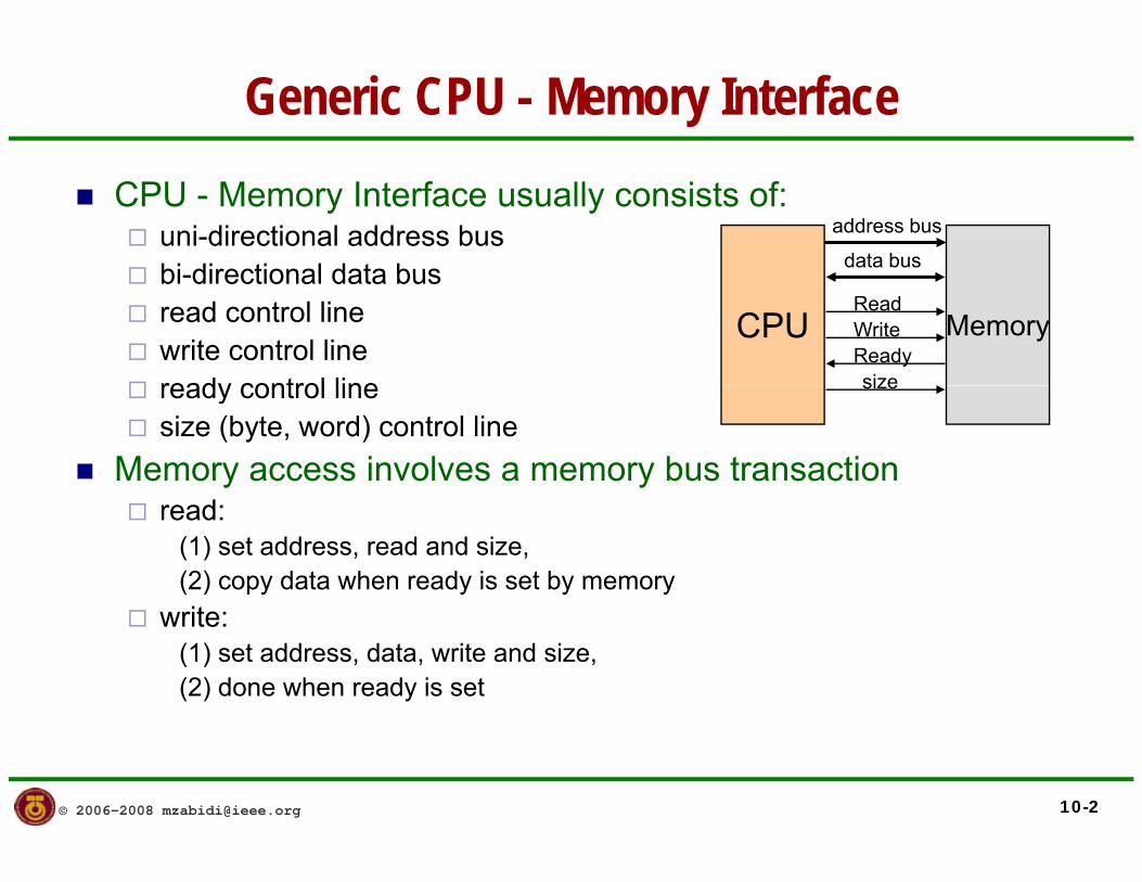
Generic CPU - Memory Interface CPU - Memory Interface usually consists of:
uni-directional address bus bi directional data bus
address bus
data busbi-directional data bus read control line write control line ready control line
CPU MemoryReadWriteReadysizeready control line
size (byte, word) control line Memory access involves a memory bus transaction
size
read: (1) set address, read and size, (2) copy data when ready is set by memory itwrite:
(1) set address, data, write and size, (2) done when ready is set
© 2006-2008 [email protected] 10-2
68000 Microprocessor
Memory Types
ROM : Read-Only MemoryNon-volatile (data retained even without power)E i llExists on all computersFunctions on embedded systems: power-on self test, monitor program, application program.Functions on general-purpose computer: power-on self test, basic input/output system (BIOS), monitor program, etc
RAM : Random Access MemoryyVolatile (data disappears without power)Functions on general purpose computer: main memory for running operating system and application programoperating system and application programFunctions on embedded systems: scratch-pad memoryMay not be required on very simple embedded systems
© 2006-2008 [email protected] 10-3
68000 Microprocessor
ROM Types
MROM : Mask-programmed read-only memoryProgrammed (contents set) at the factoryL iLow cost per unitHigh NRE (non-recurring engineering) cost
PROM : Programmable ROMgProgrammable once
EPROM : erasable programmable ROMProgrammable & erasable 1000xMust be erased using ultra-violet (UV) light before reprogrammingDevice uses expensive ceramic package & has a quartz window to p p g qallow UV to pass throughUsed for prototyping. When design is sold to customers, cheaper OTPROM is used instead.
© 2006-2008 [email protected] 10-4
68000 Microprocessor
ROM Types
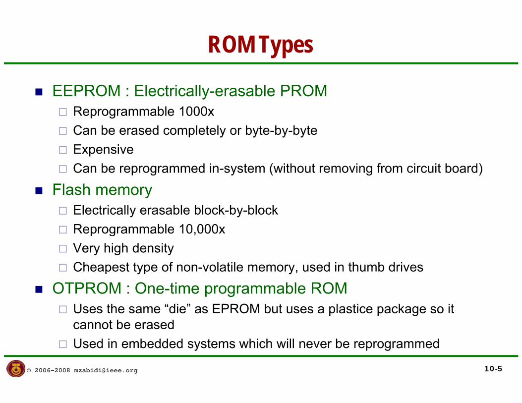
EEPROM : Electrically-erasable PROMReprogrammable 1000xC b d l l b b bCan be erased completely or byte-by-byteExpensiveCan be reprogrammed in-system (without removing from circuit board)
Flash memoryElectrically erasable block-by-blockReprogrammable 10 000xReprogrammable 10,000xVery high densityCheapest type of non-volatile memory, used in thumb drives
OTPROM : One-time programmable ROMUses the same “die” as EPROM but uses a plastice package so it cannot be erased
© 2006-2008 [email protected] 10-5
cannot be erasedUsed in embedded systems which will never be reprogrammed
68000 Microprocessor
Types of RAM
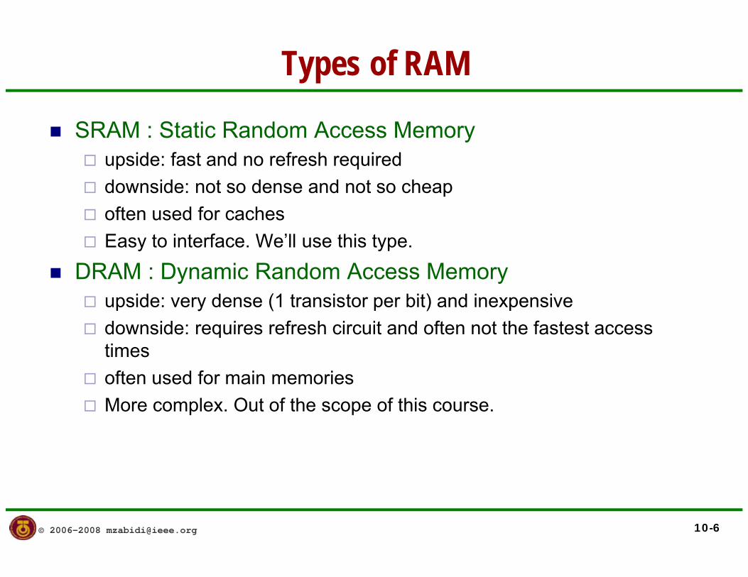
SRAM : Static Random Access Memory upside: fast and no refresh required d id d d hdownside: not so dense and not so cheap often used for caches Easy to interface. We’ll use this type.
DRAM : Dynamic Random Access Memory upside: very dense (1 transistor per bit) and inexpensive downside: requires refresh circuit and often not the fastest accessdownside: requires refresh circuit and often not the fastest access times often used for main memories M l O f h f hiMore complex. Out of the scope of this course.
© 2006-2008 [email protected] 10-6
68000 Microprocessor
Memory Organization
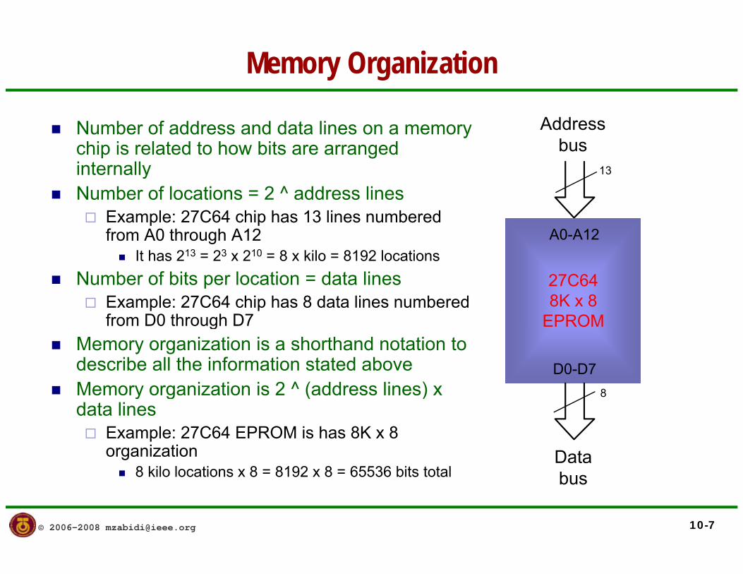
Number of address and data lines on a memory chip is related to how bits are arranged internally
Address bus
13yNumber of locations = 2 ^ address lines
Example: 27C64 chip has 13 lines numbered from A0 through A12
It h 213 23 210 8 kil 8192 l tiA0-A12
It has 213 = 23 x 210 = 8 x kilo = 8192 locationsNumber of bits per location = data lines
Example: 27C64 chip has 8 data lines numbered from D0 through D7
27C648K x 8
EPROMfrom D0 through D7Memory organization is a shorthand notation to describe all the information stated aboveMemory organization is 2 ^ (address lines) x
D0-D78
EPROM
y g ( )data lines
Example: 27C64 EPROM is has 8K x 8 organization
8 kil l ti 8 8192 8 65536 bit t t lData
8
© 2006-2008 [email protected] 10-7
8 kilo locations x 8 = 8192 x 8 = 65536 bits total bus

68000 Microprocessor
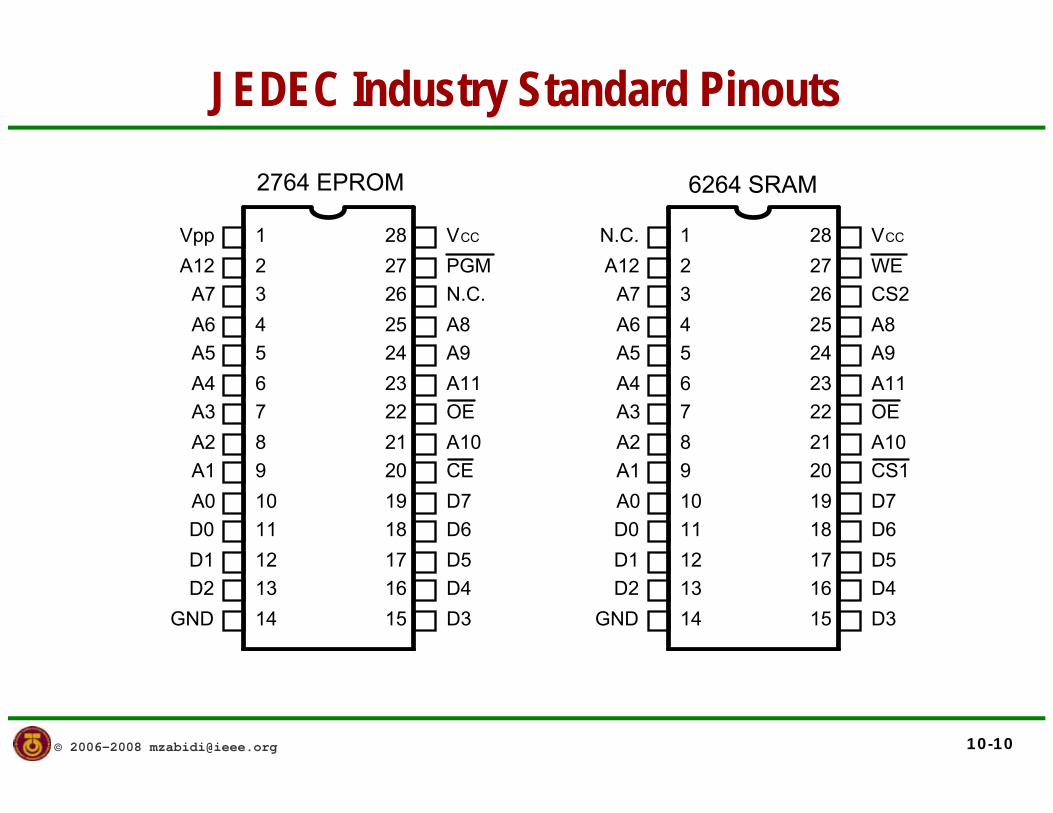
JEDEC
Joint Electronic Device Engineering CouncilSt d d i t fStandard pinout for many related memoriesInterchangeability of d i f diff tdevices from different vendors
© 2006-2008 [email protected] 10-8
68000 Microprocessor
JEDEC Industry Standard Pinouts
Vpp 1 28 VCC 1 28 VCCN.C.
2764 EPROM 6264 SRAM
A12A7A6A5 5
432 27
262524
N.C.A8A9
PGM A12A7A6A5 5
432 27
262524
CS2A8A9
WE
A5A4A3A2 8
765 24
232221
A9A11
A10OE
A5A4A3A2 8
765 24
232221
A9A11
A10OE
A1A0D0D1 12
11109 20
191817
D7D6D5
CE A1A0D0D1 12
11109 20
191817
D7D6D5
CS1
D1D2
GND 141312 17
1615
D5D4D3
D1D2
GND 141312 17
1615
D5D4D3
© 2006-2008 [email protected] 10-10
68000 Microprocessor
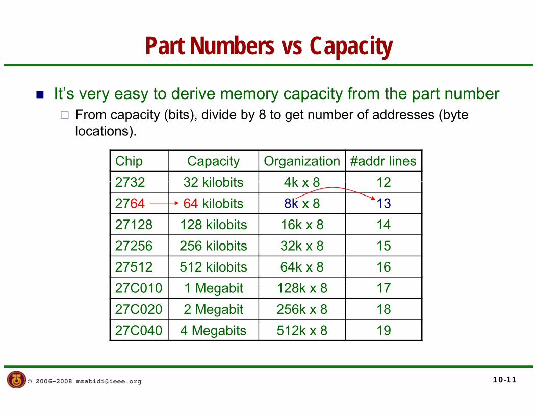
Part Numbers vs Capacity
It’s very easy to derive memory capacity from the part numberFrom capacity (bits), divide by 8 to get number of addresses (byte locations)locations).
Chip Capacity Organization #addr lines2732 32 kilobits 4k x 8 122732 32 kilobits 4k x 8 122764 64 kilobits 8k x 8 1327128 128 kilobits 16k x 8 1427256 256 kilobits 32k x 8 1527512 512 kilobits 64k x 8 1627C010 1 Megabit 128k x 8 1727C010 1 Megabit 128k x 8 1727C020 2 Megabit 256k x 8 1827C040 4 Megabits 512k x 8 19
© 2006-2008 [email protected] 10-11
68000 Microprocessor
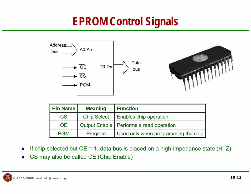
EPROM Control Signals
A0-AnAddress bus
OE
CS
D0-DmData bus
PGM
Pin Name Meaning Function
PGM
Pin Name Meaning FunctionCS Chip Select Enables chip operationOE Output Enable Performs a read operation
PGM Program Used only when programming the chip
If chip selected but OE = 1, data bus is placed on a high-impedance state (Hi-Z)CS may also be called CE (Chip Enable)
PGM Program Used only when programming the chip
© 2006-2008 [email protected] 10-12
CS may also be called CE (Chip Enable)

68000 Microprocessor
SRAM Control Signals
A0-AnAddress bus
OE
CS
D0-DmData Bus
WE
Pin Name Meaning FunctionCS Chip Select Enables chip operationOE Output Enable Performs a read operation
If OE d WE ti t th ti it ti b f d
O Output ab e e o s a ead ope at oWE Write Enable Performs a write operation
© 2006-2008 [email protected] 10-13
If OE and WE are active at the same time, a write operation be performed
68000 Microprocessor
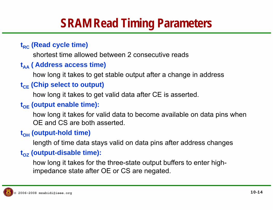
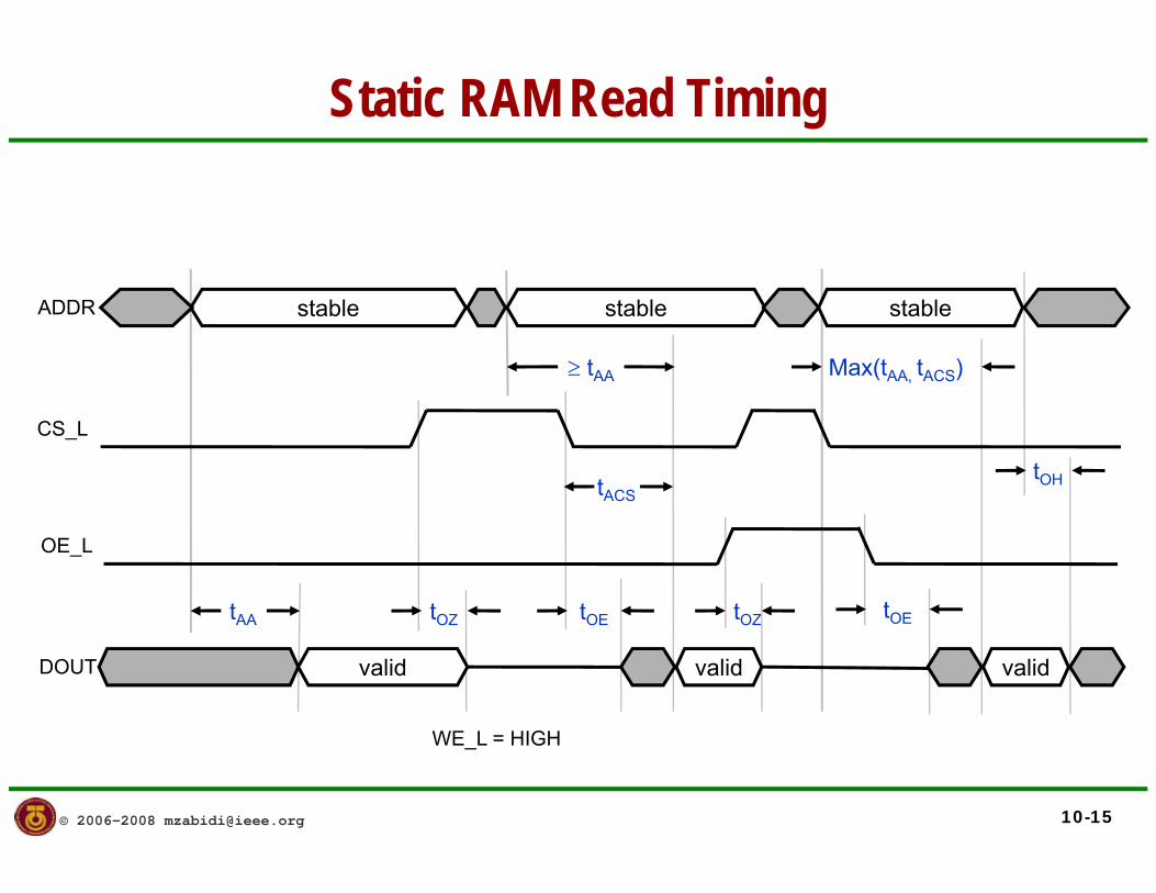
SRAM Read Timing ParameterstRC (Read cycle time)
shortest time allowed between 2 consecutive readst ( Address access time)tAA ( Address access time)
how long it takes to get stable output after a change in addresstCE (Chip select to output)
how long it takes to get valid data after CE is asserted.tOE (output enable time):
how long it takes for valid data to become available on data pins when OE and CS are both asserted.
tOH (output-hold time)length of time data stays valid on data pins after address changeslength of time data stays valid on data pins after address changes
tOZ (output-disable time): how long it takes for the three-state output buffers to enter high-impedance state after OE or CS are negated
© 2006-2008 [email protected] 10-14
impedance state after OE or CS are negated.
68000 Microprocessor
Static RAM Read Timing
stable stable stable
≥ tAA Max(tAA, tACS)
ADDR
tACStOH
CS_L
tAA tOZ tOE tOZ tOE
OE_L
valid valid valid
tAA tOZ tOE tOZ tOE
DOUT
© 2006-2008 [email protected] 10-15
WE_L = HIGH
68000 Microprocessor
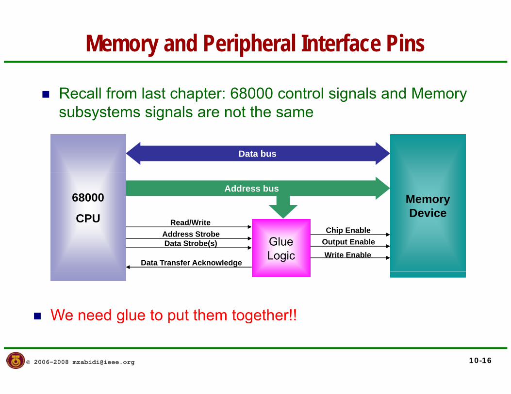
Memory and Peripheral Interface Pins
Recall from last chapter: 68000 control signals and Memory subsystems signals are not the same
Data bus
68000
CPU
Address busMemory Device
Read/WriteCPU
Glue Logic
Read/WriteAddress StrobeData Strobe(s)
Data Transfer Acknowledge
Output EnableWrite Enable
Chip Enable
We need glue to put them together!!
© 2006-2008 [email protected] 10-16
g p g
68000 Microprocessor
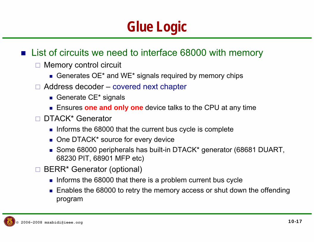
Glue LogicList of circuits we need to interface 68000 with memory
Memory control circuitGenerates OE* and WE* signals required by memory chipsGenerates OE and WE signals required by memory chips
Address decoder – covered next chapterGenerate CE* signalsE d l d i t lk t th CPU t tiEnsures one and only one device talks to the CPU at any time
DTACK* GeneratorInforms the 68000 that the current bus cycle is completeOne DTACK* source for every deviceSome 68000 peripherals has built-in DTACK* generator (68681 DUART, 68230 PIT, 68901 MFP etc)
BERR* G t ( ti l)BERR* Generator (optional)Informs the 68000 that there is a problem current bus cycleEnables the 68000 to retry the memory access or shut down the offending program
© 2006-2008 [email protected] 10-17
program

68000 Microprocessor
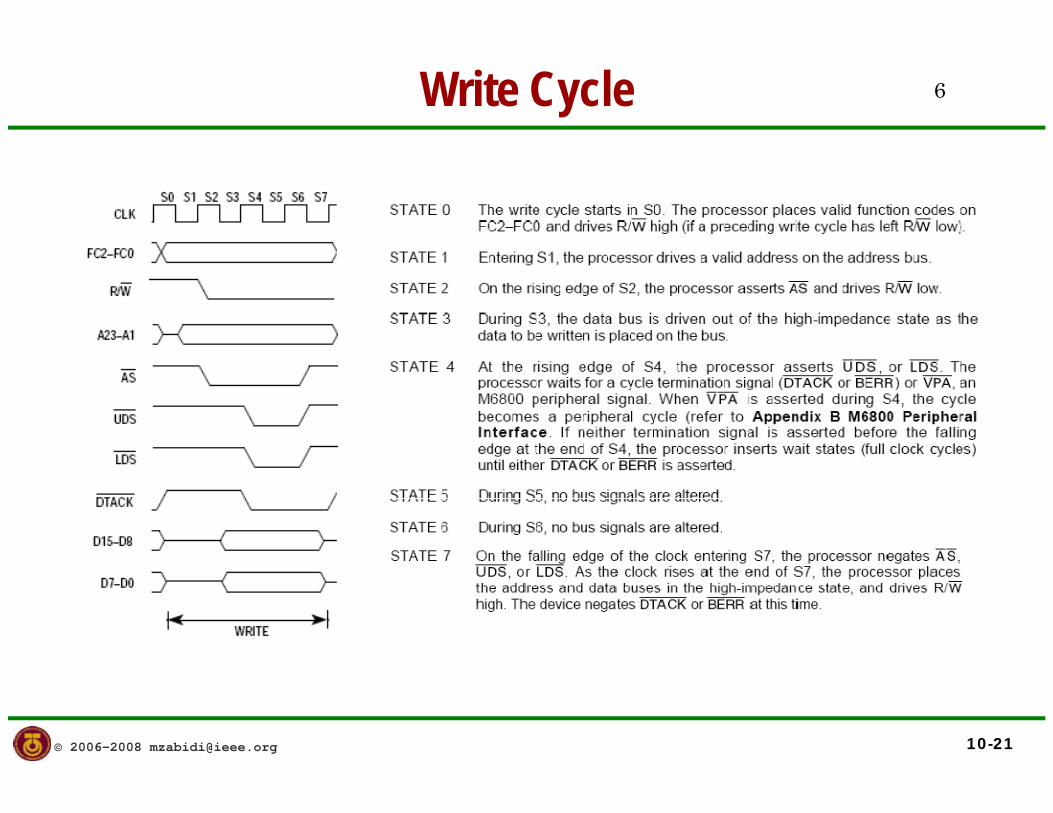
Asynchronous Bus Operation
The basic 68000 asynchronous operation isThe 68000 puts an address on the address bus and asserts Address Strobe (AS*) to signal memory and I/O devices that a valid address isStrobe (AS*) to signal memory and I/O devices that a valid address is available on the busThe memory or I/O device asserts Data Transfer Acknowledge (DTACK*) to signal the 68000 that(DTACK*) to signal the 68000 that
Valid data is available on the data bus during a read operation (the 68000 latches data when DTACK* is asserted)Data has been successfully written to the memory or I/O deviceData has been successfully written to the memory or I/O device
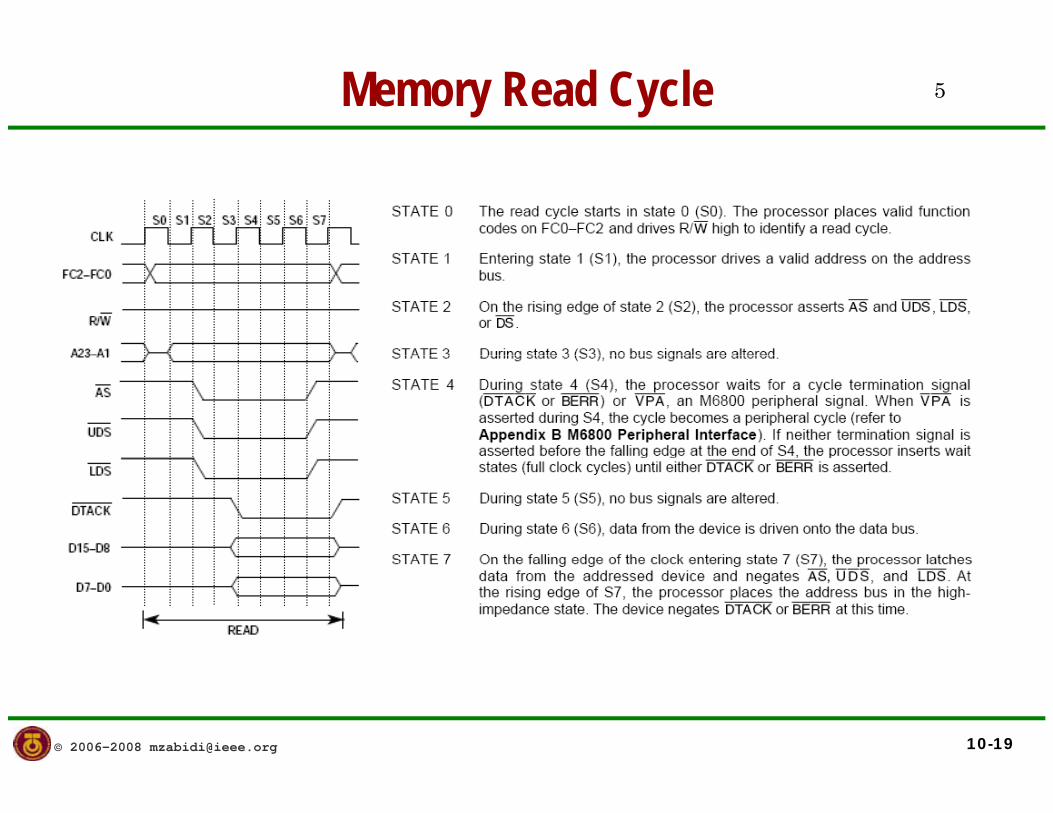
Asynchronous operation allows the 68000 to interface with slow memory or I/O memory devicesA 68000 memory access takes a minimum of eight clock states numbered from clock states S0 to S7
© 2006-2008 [email protected] 10-18
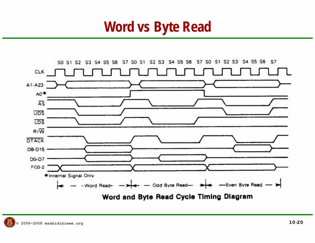
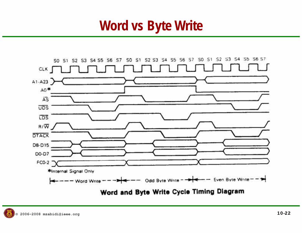
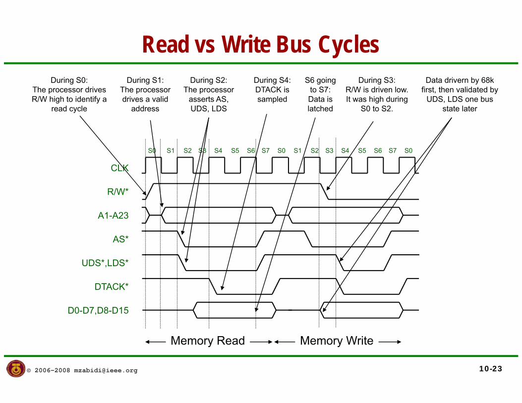
68000 Microprocessor
Read vs Write Bus CyclesDuring S0:
The processor drives R/W high to identify a
read cycle
During S1:The processor drives a valid
address
During S2:The processor
asserts AS, UDS, LDS
During S4:DTACK is sampled
S6 going to S7:Data is latched
During S3:R/W is driven low. It was high during
S0 to S2.
Data drivern by 68k first, then validated by
UDS, LDS one bus state later
CLK
S0 S1 S2 S3 S4 S5 S6 S7 S0 S1 S2 S3 S4 S5 S6 S7 S0
A1-A23
R/W*
AS*
UDS*,LDS*
DTACK*
D0-D7,D8-D15
© 2006-2008 [email protected] 10-23
Memory Read Memory Write
68000 Microprocessor
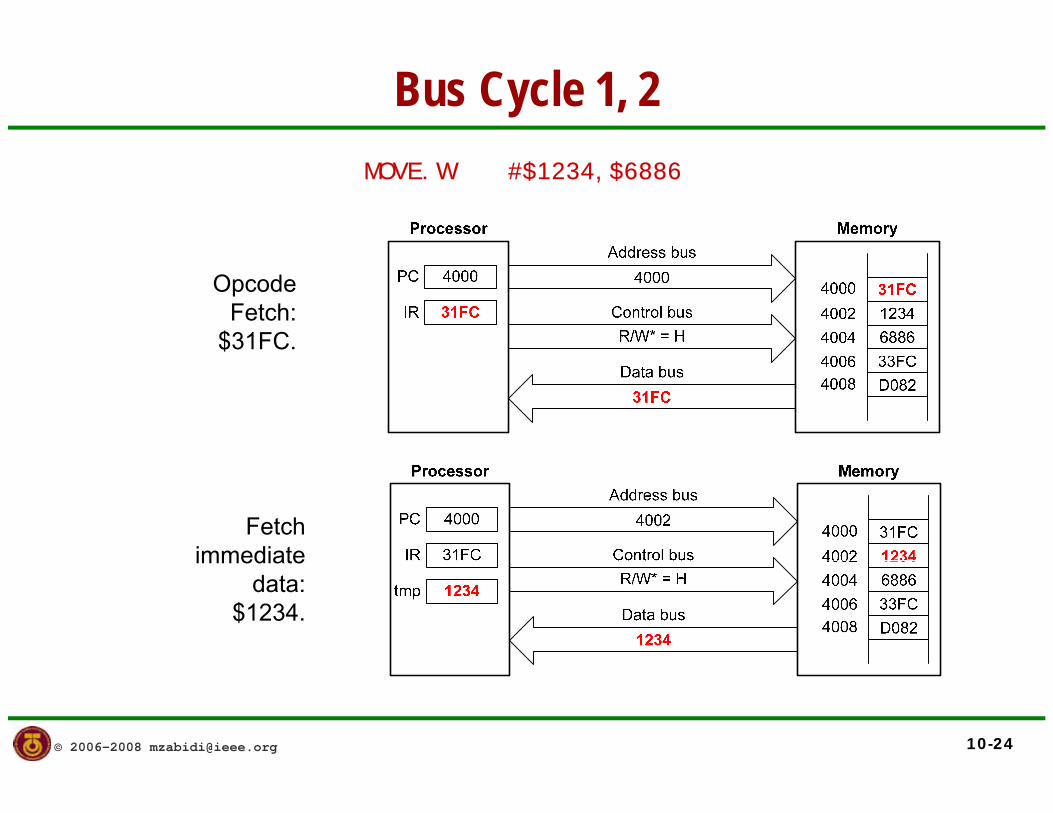
Bus Cycle 1, 2MOVE.W #$1234,$6886
Opcode Fetch:
$31FC.
Fetch immediateimmediate
data:$1234.
© 2006-2008 [email protected] 10-24

68000 Microprocessor
Bus Cycle 3,4MOVE.W #$1234,$6886
Fetch destination
address.$6886$6886
Write data to memory:memory:
© 2006-2008 [email protected] 10-25

68000 Microprocessor
Simplified Timing Relationship00001000 ORG $100000001000 303C 1234 MOVE.W #$1234,D000001004 D038 1011 ADD.B $1011,D000001008 11C0 1010 MOVE.B D0,$10100000100C 00001010 ORG $101000001010= 0031 DC W 4900001010= 0031 DC.W 4900001012 DS.W 1
Bus Cycle 1 2 3 4 5 6 7 8Bus Cycle 1 2 3 4 5 6 7 8
Addr Bus 1000 1002 1004 1006 1011 1008 100A 1010
Data Bus 303C 1234 D038 1011 --31 11C0 1010 65--
/ *R/W* H H H H H H H L
UDS L L L L H L L L
LDS L L L L L L L H
© 2006-2008 [email protected] 10-26
68000 Microprocessor
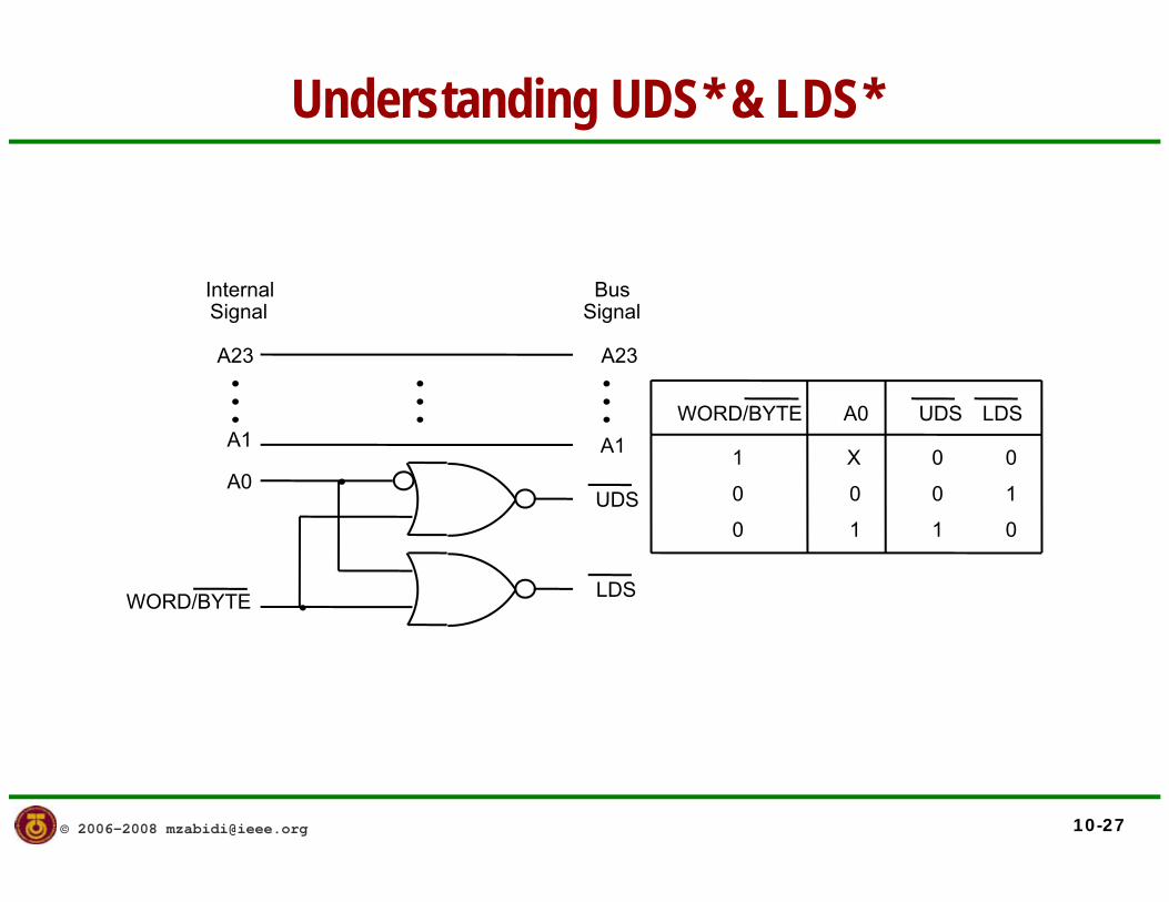
Understanding UDS* & LDS*
A23 A23
InternalSignal
Bus Signal
A1
A0
A1
UDS
WORD/BYTE LDSUDSA0
1 X 0 0
0 0 10
WORD/BYTE LDS
0 1 1 0
© 2006-2008 [email protected] 10-27

68000 Microprocessor
Understanding UDS* & LDS*
Operation UDS* LDS* R/W* Even (D8-D15)
Odd (D0-D7)
I t l PInternal Processor Operation 1 1 – No valid data No valid data
Word read 0 0 1 Valid dataBit 8-15
Valid dataBit 0-7
Read Odd byte read 1 0 1 No valid data Valid dataBit 0-7
Even byte read 0 1 1 valid dataBi 8 1 No valid dataEven byte read 0 1 1 Bit 8-15 No valid data
Word write 0 0 0 Valid dataBit 8-15
Valid dataBit 0-7
Valid data Valid dataWrite Odd byte write 1 0 0 Valid dataBit 0-7
Valid dataBit 0-7
Even byte write 0 1 0 Valid dataBit 8-15
Valid dataBit 8-15
© 2006-2008 [email protected] 10-28
We must not activate the wrong memory chip during byte writes.
68000 Microprocessor
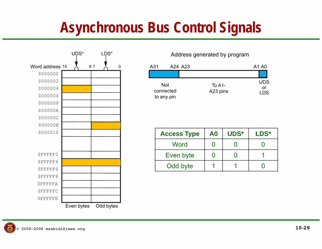
Asynchronous Bus Control Signals
A0A1A23A24A31
Address generated by program
07815
$000000
UDS* LDS*
Word address
To A1-A23 pins
Not connected to any pin
UDS or
LDS
$000002
$000004
$000006
$000008
$00000$00000A
$00000C
$00000E
$000010 Access Type A0 UDS* LDS*
$FFFFF2
$FFFFF4
$FFFFF6
Word 0 0 0Even byte 0 0 1Odd byte 1 1 0
$FFFFF8
$FFFFFA
$FFFFFC
$FFFFFE
© 2006-2008 [email protected] 10-29
Even bytes Odd bytes

68000 Microprocessor
Memory Control Logic
To OE* pin of even UDS*
To OE* pin of odd
(upper) memory chipsUPRD*
LORD*
UDS
LDS*
To WE* pin of even
(lower) memory chipsLORD
UPWR* p(upper) memory chips
To WE* pin of odd LOWR*R/W* (lower) memory chipsR/W
© 2006-2008 [email protected] 10-30
68000 Microprocessor
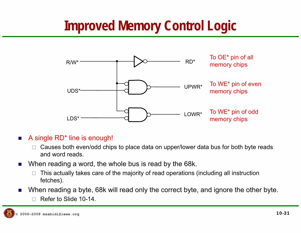
Improved Memory Control Logic
RD*R/W*To OE* pin of all memory chips
UPWR*UDS*
To WE* pin of even memory chips
LOWR*LDS*
To WE* pin of odd memory chips
A single RD* line is enough!Causes both even/odd chips to place data on upper/lower data bus for both byte reads and word reads.
When reading a word, the whole bus is read by the 68k.This actually takes care of the majority of read operations (including all instruction fetches).
When reading a byte 68k will read only the correct byte and ignore the other byte
© 2006-2008 [email protected] 10-31
When reading a byte, 68k will read only the correct byte, and ignore the other byte. Refer to Slide 10-14.
68000 Microprocessor
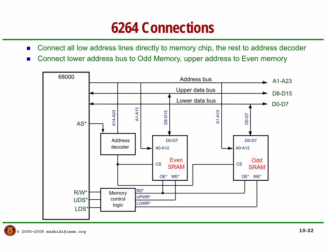
6264 ConnectionsConnect all low address lines directly to memory chip the rest to address decoderConnect all low address lines directly to memory chip, the rest to address decoderConnect lower address bus to Odd Memory, upper address to Even memory
68000 Address bus A1-A23
D8-D15
D0-D7
68000
3 3 3
Address bus
Upper data bus
Lower data bus
Address
A14
-A23
A1-
A1
D8-
D15
D0-
D7
D0-D7 D0-D7
A1-
A13
AS*
EvenSRAM
Addressdecoder
CS CS
A0-A12 A0-A12
OddSRAM
UDS*Memory controllogic
OE* WE* OE* WE*
R/W* RD*UPWR*LOWR*
© 2006-2008 [email protected] 10-32
LDS*logic

68000 Microprocessor
Connections From RAM & ROM Sidem
680
00Fr
om
A0
A1
A2
A3
A4
A5
A6
A7
A8
A9
A10
A11
A12
A0
A1
A2
A3
A4
A5
A6
A7
A8
A9
A10
A11
A12
D0
D1
D2
D3
D4
D5
D6
D7
D0
D1
D2
D3
D4
D5
D6
D7
A0
A1
A2
A3
A4
A5
A6
A7
A8
A9
A10
A11
A12
D0
D1
D2
D3
D4
D5
D6
D7
A0
A1
A2
A3
A4
A5
A6
A7
A8
A9
A10
A11
A12
D0
D1
D2
D3
D4
D5
D6
D7
From
glu
e lo
gic
pper
dat
a bu
s
m 6
8000
Up
Low
er d
ata
busFrom
© 2006-2008 [email protected] 10-33
L

68000 Microprocessor
Wait StatesDepending on the speed of your processor, the access times of your memory and peripheral chips, it may be necessary to add a few clock cycles into the 68000’s bus cycle. cyc es o e 68000 s bus cyc eThe extra cycles are called wait statesThis gives slower devices time to respond. Wait states are used only for the slow devices; fast devices still run at full speedthe slow devices; fast devices still run at full speed.For 68000, DTACK* input high causes the processor to wait. To insert a wait state for a given device…
d t d t t t th t d iwe need to detect an access to that device…and hold DTACK* inactive for the required additional clock cycles.
In other words, use the chip select for a given device to delay DTACK* i lgoing low.
Today fast memory is cheap, so knowing how generate DTACK delay is
© 2006-2008 [email protected] 10-34
not that important any more…
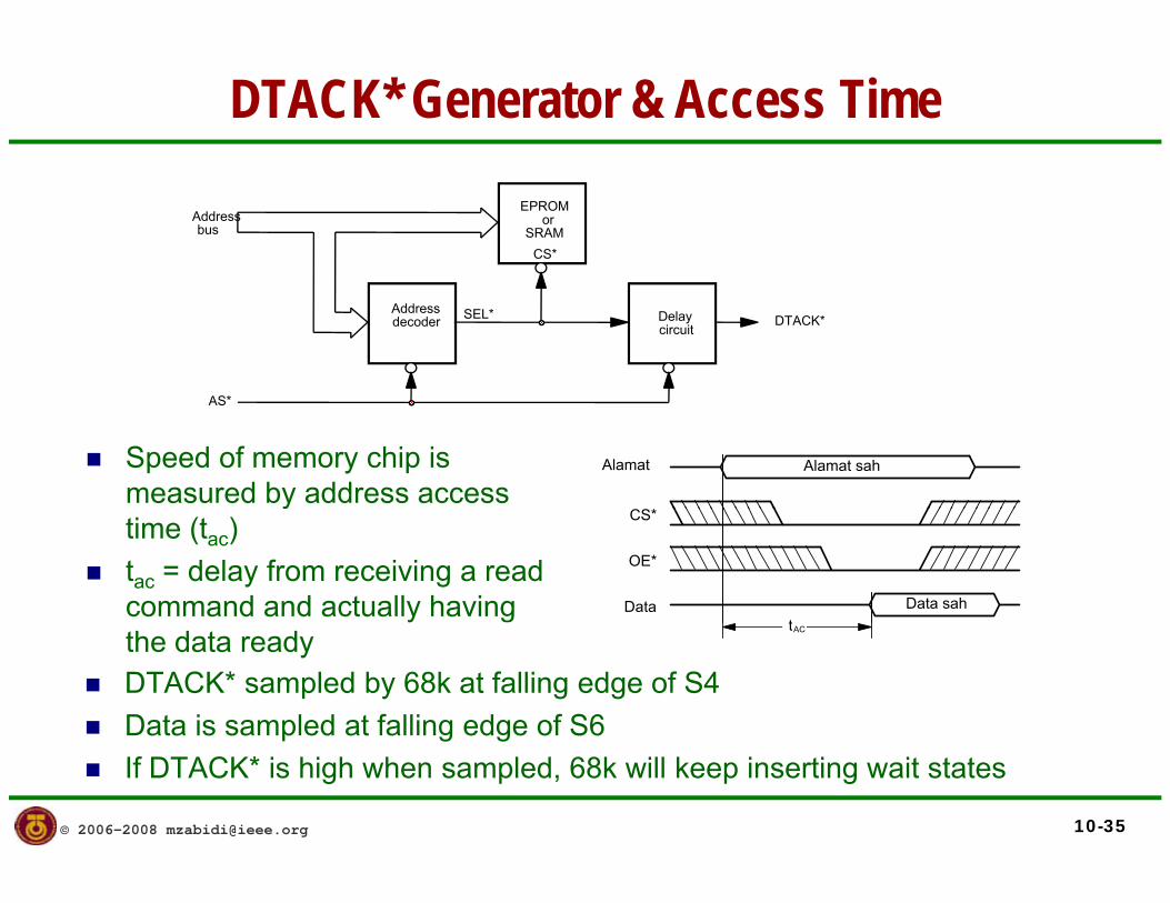
68000 Microprocessor
DTACK* Generator & Access TimeEPROM
orSRAM
CS*
Addressbus
SEL*Address decoder Delay
circuitDTACK*
Alamat Alamat sahSpeed of memory chip is measured by address access
AS*
CS*
OE*
Data Data saht
ytime (tac)tac = delay from receiving a read command and actually having
DTACK* sampled by 68k at falling edge of S4Data is sampled at falling edge of S6
tAC
the data ready
© 2006-2008 [email protected] 10-35
p g gIf DTACK* is high when sampled, 68k will keep inserting wait states
68000 Microprocessor
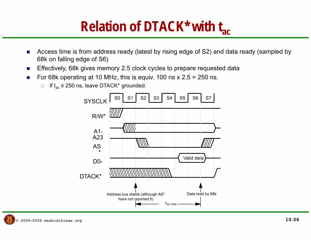
Relation of DTACK* with tac
Access time is from address ready (latest by rising edge of S2) and data ready (sampled by 68k on falling edge of S6)Effectively, 68k gives memory 2.5 clock cycles to prepare requested dataFor 68k operating at 10 MHz, this is equiv. 100 ns x 2.5 = 250 ns.
If tac ≤ 250 ns, leave DTACK* grounded.
SYSCLK S0 S1 S2 S3 S4 S5 S7S6
A1-A23
R/W*
A23AS
*D0- Valid data
DTACK*
Address bus stable (although AS* Data read by 68k
© 2006-2008 [email protected] 10-36
( ghave not reported it)
y
tac max
68000 Microprocessor
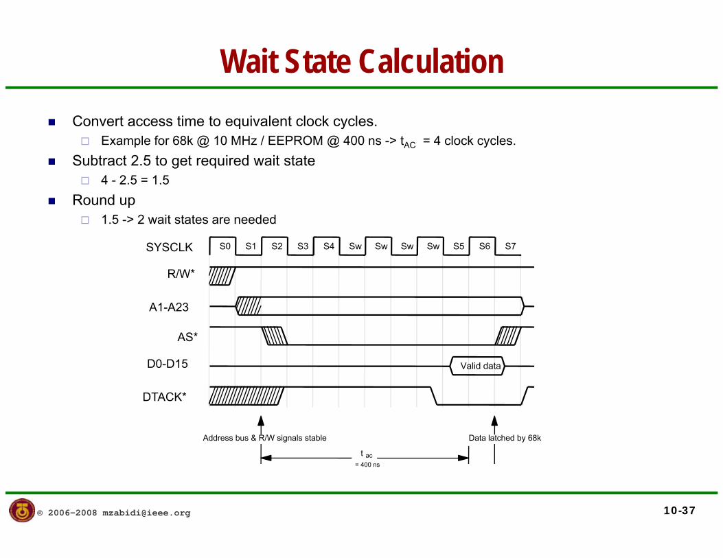
Wait State CalculationConvert access time to equivalent clock cycles.
Example for 68k @ 10 MHz / EEPROM @ 400 ns -> tAC = 4 clock cycles.Subtract 2.5 to get required wait state
4 - 2.5 = 1.5Round up
1.5 -> 2 wait states are needed
SYSCLK S0 S1 S2 S3 S4 S S S S5 S7S6SSYSCLK
A1-A23
R/W*
S0 S1 S2 S3 S4 Sw Sw Sw S5 S7S6Sw
AS*
D0-D15 Valid data
DTACK*
Address bus & R/W signals stable Data latched by 68k
t ac
© 2006-2008 [email protected] 10-37
t ac = 400 ns

68000 Microprocessor
Example DTACK* Circuit for 4 Wait States
AS*
1WAIT
SEL* D DPRE PREQ Q DTACK*
CLK CLK
1WAIT
SYSCLK
CLK CLK
“1” “1”
SYSCLK
SEL*SEL*
DTACK*
1WAIT
© 2006-2008 [email protected] 10-38
DTACK
68000 Microprocessor
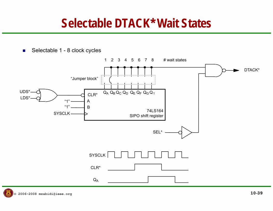
Selectable DTACK* Wait States
Selectable 1 - 8 clock cycles1 2 3 4 5 6 7 8 # wait states
Q
DTACK*
Q QC Q Q Q QG Q
“Jumper block”
UDS*
SYSCLK
CLR* QA QB QC QD QE QF QG Q1
AB
“1”“1”
74LS164SIPO shift register
UDSLDS*
SEL*
CLR*
SYSCLK
© 2006-2008 [email protected] 10-39
QA
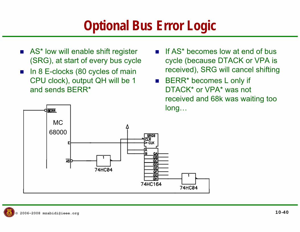
68000 Microprocessor
Optional Bus Error LogicAS* low will enable shift register (SRG), at start of every bus cycleIn 8 E-clocks (80 cycles of main
If AS* becomes low at end of bus cycle (because DTACK or VPA is received), SRG will cancel shiftingIn 8 E-clocks (80 cycles of main
CPU clock), output QH will be 1 and sends BERR*
ece ed), S G ca ce s gBERR* becomes L only if DTACK* or VPA* was not received and 68k was waiting too glong…
MC6800068000
© 2006-2008 [email protected] 10-40
Related Documents