Manual EN PEM575 Universal measuring device Software version 2.00.xx PEM575_D00016_01_M_XXEN/05.2016 B 9310 0575 B 9310 0576 B 9310 0577 B 9310 0578 B 9310 0579 B 9310 0580

Welcome message from author
This document is posted to help you gain knowledge. Please leave a comment to let me know what you think about it! Share it to your friends and learn new things together.
Transcript
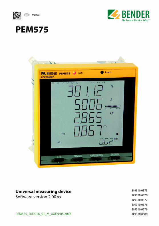
ManualEN
PEM575
Universal measuring deviceSoftware version 2.00.xx
PEM575_D00016_01_M_XXEN/05.2016
B 9310 0575
B 9310 0576
B 9310 0577
B 9310 0578
B 9310 0579
B 9310 0580

Bender GmbH & Co. KGLondorfer Str. 65 • 35305 Gruenberg • GermanyPostfach 1161 • 35301 Gruenberg • Germany
Tel.: +49 6401 807-0Fax: +49 6401 807-259
E-Mail: [email protected]
© Bender GmbH & Co. KG
All rights reserved.Reprinting only with permission
of the publisher. Subject to change!Photos: Bender

Table of Contents
1. Making effective use of this document ............................................... 9
1.1 How to use this manual ......................................................................................... 9
1.2 Technical support: Service and support ........................................................ 10
1.3 Workshops ............................................................................................................... 11
1.4 Delivery conditions, guarantee, warranty and liability ............................ 11
2. Safety ...................................................................................................... 13
2.1 Intended use ........................................................................................................... 13
2.2 Qualified personnel .............................................................................................. 13
2.3 General safety instructions ................................................................................ 14
3. Device description ............................................................................... 15
3.1 Area of application ................................................................................................ 15
3.2 Device features ....................................................................................................... 15
3.3 Versions ..................................................................................................................... 16
3.4 Application example ............................................................................................ 17
3.5 Description of function ....................................................................................... 17
3.6 Front view and rear view .................................................................................... 18
4. Installation and connection ............................................................... 19
4.1 Project planning ..................................................................................................... 19
4.2 Safety instructions ................................................................................................. 19
4.3 Installing the device ............................................................................................. 19
4.3.1 Dimension diagrams ................................................................................... 194.3.2 Front panel mounting ................................................................................ 20
4.4 Connection of the device ................................................................................... 21
4.4.1 Safety information ....................................................................................... 214.4.2 Back-up fuses ................................................................................................. 214.4.3 Connection of measuring current transformers ............................... 21
3PEM575_D00016_01_M_XXEN/05.2016
Table of Contents
4.5 Instructions for connection ................................................................................ 21
4.6 Wiring diagram ....................................................................................................... 22
4.7 Connection diagram voltage inputs ............................................................... 23
4.7.1 Three-phase 4-wire system (TN, TT, IT system) .................................. 234.7.2 Three-phase 3-wire system ....................................................................... 244.7.3 Connection via voltage transformers ................................................... 25
4.8 Digital inputs ........................................................................................................... 25
4.9 Digital outputs ........................................................................................................ 26
4.10 Modbus TCP (connector pin assignment) .................................................... 26
5. Commissioning ...................................................................................... 27
5.1 Check proper connection ................................................................................... 27
5.2 Before switching on .............................................................................................. 27
5.3 Switching on ............................................................................................................ 27
5.4 System ....................................................................................................................... 27
6. Operation ............................................................................................... 29
6.1 Getting to know the operating elements .................................................... 29
6.2 LCD testing ............................................................................................................... 30
6.3 Getting to know standard display areas ....................................................... 30
6.4 Power and current demands (demand display) ......................................... 32
6.5 LED indication ......................................................................................................... 34
6.6 Standard display .................................................................................................... 34
6.7 Data display ............................................................................................................. 34
6.7.1 "V/I" button ..................................................................................................... 356.7.2 "POWER"button ............................................................................................ 376.7.3 "HARMONICS" button ................................................................................. 396.7.4 "ENERGY" button .......................................................................................... 40
6.8 Setup configuration via the front panel ........................................................ 41
6.8.1 Setup: Function of buttons ....................................................................... 416.8.2 Setup: Overview diagram menu ............................................................. 42
6.9 Setup: adjustment possibilities ........................................................................ 43
6.10 Configuration example: ....................................................................................... 49
4 PEM575_D00016_01_M_XXEN/05.2016
Table of Contents
7. Application/inputs and outputs ......................................................... 51
7.1 Digital inputs (DI) ................................................................................................... 51
7.2 Digital outputs (DO) ............................................................................................. 51
7.3 Energy pulsing output ......................................................................................... 52
7.4 Power and energy ................................................................................................. 52
7.4.1 Basic measurements ................................................................................... 527.4.2 High-speed measurements ...................................................................... 537.4.3 Voltage and current phase angles ......................................................... 537.4.4 Energy .............................................................................................................. 53
7.5 Demand DMD ......................................................................................................... 53
7.5.1 Max/Min values per demand period ..................................................... 55
7.6 Setpoints ................................................................................................................... 55
7.7 Logic modules ........................................................................................................ 59
8. Logging ................................................................................................... 61
8.1 Peak demand log ................................................................................................... 61
8.2 Max/Min log ............................................................................................................. 61
8.3 Data recorder (DR) ................................................................................................. 62
8.3.1 Setup parameters ......................................................................................... 638.3.2 Selectable measured quantities for data recorders DR .................. 64
8.4 Energy log ................................................................................................................ 76
8.5 Waveform recording (WFR) ................................................................................ 77
8.6 Power Quality log (PQ log) ................................................................................. 78
8.7 Event log (SOE log) ................................................................................................ 79
9. Power Quality ........................................................................................ 81
9.1 Fundamentals ......................................................................................................... 81
9.2 Harmonic distortion .............................................................................................. 81
9.3 Deviation from the pre-set nominal value (ΔU, Δ❆) .................................. 83
9.4 Undervoltage/overvoltage setpoint (sag/swell setpoint) ...................... 84
9.5 Transient events setpoint ................................................................................... 84
9.6 Time synchronisation ........................................................................................... 84
5 PEM575_D00016_01_M_XXEN/05.2016
Table of Contents
10. Modbus Register Map ........................................................................ 85
10.1 Basic measurements ............................................................................................. 87
10.2 Energy measurement ........................................................................................... 91
10.3 Pulse counter .......................................................................................................... 92
10.4 Fundamental measurements (Power quality) ............................................. 93
10.5 Harmonic measurements (Power quality) .................................................... 95
10.6 High-speed measurement ................................................................................. 97
10.7 Demand ..................................................................................................................... 99
10.7.1 Present demand ........................................................................................... 9910.7.2 Predicted demand .................................................................................... 10010.7.3 Maximum values per demand period ............................................... 10210.7.4 Minimum values per demand period ................................................ 10410.7.5 Peak demand of this month .................................................................. 10610.7.6 Peak demand last month ....................................................................... 10610.7.7 Peak demand data structure ................................................................. 107
10.8 Max/Min log .......................................................................................................... 108
10.8.1 Maximum values of this month .......................................................... 10810.8.2 Min log of this month .............................................................................. 11010.8.3 Max log of last month .............................................................................. 11210.8.4 Min log last month .................................................................................... 11410.8.5 Max/Min log data structure ................................................................... 115
10.9 Setup parameters ............................................................................................... 116
10.10 Clear/reset register ............................................................................................. 121
10.11 Setpoint setup parameters ............................................................................. 123
10.11.1 Structure of the setpoint register (standard) .................................. 12410.11.2 Setpoint register structure (high speed) ........................................... 124
10.12 Logic module ....................................................................................................... 127
10.12.1 Logic module registers ............................................................................ 12710.12.2 Logic module data structure ................................................................. 127
10.13 Data recorder (DR) .............................................................................................. 129
10.13.1 Data recorder register .............................................................................. 12910.13.2 High-speed data recorder register structure .................................. 13010.13.3 Standard data recorder register structure ....................................... 132
10.14 Waveform recording (WFR) ............................................................................. 133
6 PEM575_D00016_01_M_XXEN/05.2016
Table of Contents
10.15 Energy log ............................................................................................................. 136
10.16 PQ log ..................................................................................................................... 138
10.17 Event log (SOE log) ............................................................................................. 139
10.17.1 Energy log register .................................................................................... 14010.17.2 Event log data structure ......................................................................... 14010.17.3 Event classification (SOE log) ............................................................... 141
10.18 Time setting .......................................................................................................... 151
10.19 DOx output control ........................................................................................... 152
10.20 Universal measuring device information ................................................... 153
11. Technical data .................................................................................. 155
11.1 Standards and certifications ........................................................................... 157
11.2 Ordering information ........................................................................................ 157
INDEX ......................................................................................................... 159
7 PEM575_D00016_01_M_XXEN/05.2016


1. Making effective use of this document
1.1 How to use this manualThis manual is aimed at qualified personnel in electrical engineering and communications technology, installers and users of the product and must be kept ready for referencing in the immediate vicinity of the device. To make it easier for you to understand and revisit certain sections of text and instructions in the manual, we have used symbols to identify important instructions and information. The meaning of these symbols is explained below:
Although great care has been taken in the drafting of this operating manual, it may nevertheless contain errors and mistakes. Bender cannot accept any liability for injury to persons or damage to property resulting from errors or mistakes in this manual.Each of the registered trademarks which appears in this document remains the property of its owner.
The signal word indicates that there is a high risk of danger,, that willresult in death or serious injury if not avoided.
This signal word indicates a medium risk of danger that can lead todeath or serious injury if not avoided.
This signal word indicates a low level risk that can result in minor ormoderate injury or damage to property if not avoided.
This symbol denotes information intended to assist the user in makingoptimum use of the product.
DANGER
WARNING
CAUTION
9PEM575_D00016_01_M_XXEN/05.2016

Making effective use of this document
1.2 Technical support: Service and supportFor commissioning and troubleshooting Bender offers you:
First level supportTechnical support by phone or e-mail for all Bender products All questions about customer applications Commissioning Troubleshooting
Phone: +49 6401 807-760*Fax: +49 6401 807-259only available in Germany: 0700BenderHelp (Tel. and Fax)E-mail: [email protected]
Repair serviceRepair, calibration, update and replacement service for all Bender products Repair, calibration, testing and analysing Bender products Hardware and software update for Bender devices Delivery of replacement devices for faulty or incorrectly delivered Bender devices Extended warranty for Bender devices with in-house repair service resp. replace-
ment devices at no extra cost
Phone: +49 6401 807-780** (technical issues) +49 6401 807-784**, -785** (commercial matters)
Fax: +49 6401 807-789E-mail: [email protected]
Please send the devices for repair to the following address:
Bender GmbH, Repair Service Londorfer Strasse 65 35305 Gruenberg, Germany
10 PEM575_D00016_01_M_XXEN/05.2016

Making effective use of this document
Field serviceOn-site service for all Bender products Commissioning, parameter setting, maintenance, trouble shooting for Bender
products Analysis of the electrical installation in the building (power quality test, EMC test,
thermography) Practical training courses for customers
Phone: +49 6401 807-752**, -762 **(technical issues) +49 6401 807-753** (commercial matters)
Fax: +49 6401 807-759E-mail: [email protected]: www.bender.de.
*Available from 7.00 a.m. to 8.00 p.m. on 365 days of the year (CET/UTC+1)**Mo-Thu 7.00 a.m. - 8.00 p.m., Fr 7.00 a.m. - 13.00 p.m.
1.3 WorkshopsBender would be happy to provide training in respect of the use of the universal measuring device. Current dates of training courses and workshops can be found on the Internet at www.bender.de -> Know-how -> Seminars.
1.4 Delivery conditions, guarantee, warranty and liabilityThe conditions of sale and delivery set out by Bender apply. For software products, the "Softwareklausel zur Überlassung von Standard- Software als Teil von Lieferungen, Ergänzung und Änderung der Allgemeinen Lieferbedingungen für Erzeugnisse und Leistungen der Elektroindustrie" (software clause in respect of the licensing of standard software as part of deliveries, modifications and changes to general delivery conditions for products and services in the electrical industry) set out by the ZVEI (Zentralverband Elektrotechnik- und Elektronikindustrie e.V., (German Electrical and Electronic Manufacturers' Association) also applies.Conditions of sale and delivery can be obtained from Bender in printed or electronic format.
11PEM575_D00016_01_M_XXEN/05.2016

Making effective use of this document
12 PEM575_D00016_01_M_XXEN/05.2016

2. Safety
2.1 Intended useThe universal measuring device PEM575 is suitable for the analysis of energy and power monitoring of the power supply quality data recording for energy management. As a compact device for front panel mounting, it is a replacement for analogue indicating instruments. Das PEM575 is suitable for 2, 3 and 4-wire systems and can be used in TN, TT and IT systems. The current measurement inputs of the PEM are connected via external …/1 A or…./5 A measuring current transformers. In principle, measurements in medium and high voltage systems are carried out via measurement transformers and voltage transformers.Use for the intended purpose also includes: Device-specific settings according to local equipment and operating conditions. The observation of all information in the operating manual.
2.2 Qualified personnel
Electrically skilled persons are those who have the relevant education, knowledge and experience, as well as knowledge of the relevant safety standards and who are able to perceive risks and to avoid hazards which electricity can create when work activities are carried out on electrical installations. The electrically skilled person is specially trained for carrying out work activities in his specific working environment and has a thorough knowledge of the relevant standards and regulations. In Germany, an electrically skilled person must meet the requirements of the accident prevention regulation BGV A3. In other countries the applicable regulations have to be observed and followed.
Only electrically skilled persons are authorised to install andcommission this device.
13PEM575_D00016_01_M_XXEN/05.2016

Safety
2.3 General safety instructionsBender devices are designed and built in accordance with the state of the art and accepted rules in respect of technical safety. However, the use of such devices may introduce risks to the life and limb of the user or third parties and/or result in damage to Bender equipment or other property.
Only use Bender equipment:– as intended– in perfect working order– in compliance with the accident prevention regulations and guidelines appli-
cable at the location of use Eliminate all faults immediately which may endanger safety. Do not make any unauthorised changes and only use replacement parts and opti-
onal accessories purchased from or recommended by the manufacturer of the equipment. Failure to observe this requirement can result in fire, electric shock and injury.
Information plates must always be clearly legible. Replace damaged or illegible plates immediately.
If the device is overloaded by overvoltage or a short-circuit current load, it must be checked and replaced if necessary.
If the device is being used in a location outside the Federal Republic of Germany, the applicable local standards and regulations must be complied with. European standard EN 50110 can be used as a guide.
Danger of electric shock!Touching live parts will cause danger of electric shock with fatalconsequences. All work activities on electrical installations as well as installationactivities, commissioning activities and work activities with the device inoperation may only be carried out by electrically skilled persons!
DANGER
14 PEM575_D00016_01_M_XXEN/05.2016

3. Device description
3.1 Area of applicationFor humans, electric current is not immediately visible. Universal measuring devices for monitoring electrical parameters are used wherever energy consumption, performance measurements or the quality of the supply voltage are to be made visible.The PEM575 is suitable for monitoring power generation systems (PV systems, CHPs, hydro power and wind power
plants) energy-intensive equipment and parts of installation sensitive equipment
3.2 Device featuresThe universal measuring device PEM575 for power quality and energy management is characterised by the following features: Accuracy class in accordance withIEC 62053-22: 0.2 S Password protection 16 programmable setpoints LED pulse outputs for active and reactive energy Modbus RTU communication via RS-485 interface 6 digital inputs 3 digital outputs Power and current demands for particular time frames Peak demands with timestamps Individual, current/voltage harmonics up to the 63rd harmonic Max and Min values High-resolution waveform recording (12.8 kHz) Data recorder Event log: 512 events, setup changes, setpoint alarming, DI status changes, DO
switching operations Sag/swell detection Detection of transient events Communication:
15PEM575_D00016_01_M_XXEN/05.2016
Device description
– Galvanically isolated RS-485 interface (1,200 … 19,200 bit/s)– Modbus/RTU protocol– Modbus/TCP (10/100 Mbit/s)
Measured quantities– Phase voltages UL1, UL2, UL3 in V– Line-to-line voltages UL1L2, UL2L3, UL3L1 in V– Phase currents I1, I2, I3 in A– Neutral current (calculated) I0 in A – Neutral current (measured) I4 in A – Frequency f in Hz– Phase angle for U and I in °– Power per phase conductor P in kW, Q in kvar, S in kVA– Total power P in kW, Q in kvar, S in kVA– Displacement factor cos (φ)– Power factor λ– Active and reactive energy import in kWh, kvarh– Active and reactive energy export in kWh, kvarh– Voltage unbalance in %– Current unbalance in %– Harmonic distortion
(THD, TOHD, TEHD) for U and I– K-factor for I
3.3 Versions
Type Nominal system voltage 3(N)AC Current input
PEM575 230/400 V 5 A
PEM575-251 230/400 V 1 A
PEM575-455 400/690 V 5 A
PEM575-451 400/690 V 1 A
PEM575-155 69/120 V 5 A
PEM575-151 69/120 V 1 A
16 PEM575_D00016_01_M_XXEN/05.2016
Device description
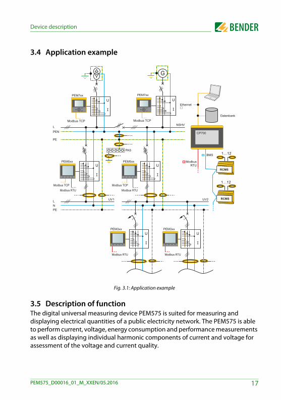
3.4 Application example
Fig. 3.1: Application example
3.5 Description of functionThe digital universal measuring device PEM575 is suited for measuring and displaying electrical quantities of a public electricity network. The PEM575 is able to perform current, voltage, energy consumption and performance measurements as well as displaying individual harmonic components of current and voltage for assessment of the voltage and current quality.
Modbus TCP
Ethernet
BMS 1…12
ModbusRTU
Datenbank
LPEN
PE
LNPE
U
I
Modbus TCPModbus RTU
PAS
PEM7xx
U
I
NSHV
UV1
1…12
RCMSUV2
U
I
U
I
U
I
RCMS
Modbus TCPModbus RTU
Modbus TCP
PEM5xx PEM5xx
Modbus RTU
PEM3xx
PEM7xx
CP700
3
U
I
Modbus RTU
PEM3xx
3
17PEM575_D00016_01_M_XXEN/05.2016
Device description
The accuracy of the active energy metering corresponds to class 0.2 S in compliance with the DIN EN 62053-22 (VDE 0418 Part 3-22):2003-11.
The large display of the panel mounting device makes the relevant measured quantities easily legible and enables fast configuration. In addition, the RS-485 interface allows a central evaluation and processing of data. Switching operations can be monitored or initiated via the digital inputs and outputs (Example: Switching off uncritical loads if the peak load limit value is exceeded).
The universal measuring device PEM575 provides the following functions: Provision of energy consumption data for a well-thought-out energy manage-
ment Allocation of energy costs Power quality monitoring for cost reduction and increased plant availability High-resolution waveform recording allow analysis of power quality phenomena
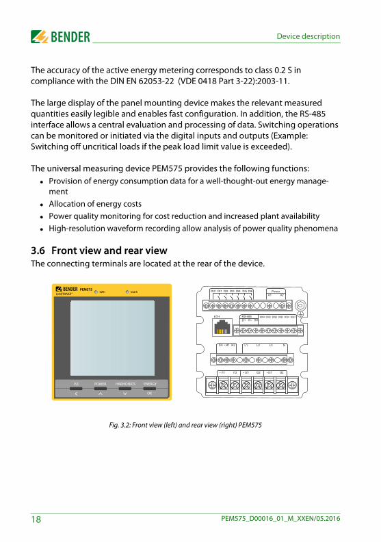
3.6 Front view and rear viewThe connecting terminals are located at the rear of the device.
Fig. 3.2: Front view (left) and rear view (right) PEM575
kvarhkWhPEM575
LINETRAXX®
V/I POWER HARMONICS ENERGY
OK
D+
DIC DI1 DI2 DI3 DI4 DI5 DI6A1 A2
Power
RS-485ETHD- SH
• l11
• l41
l12
l42SH
l22 l32
L1 L2 L3 N
• l21 • l31
DO34 DO33 DO24 DO23 DO14 DO13
18 PEM575_D00016_01_M_XXEN/05.2016

4. Installation and connection
4.1 Project planningFor any questions associated with project planning, please contact Bender:Internet: www.bender.deTel.: +49-6401-807-0
4.2 Safety instructionsOnly electrically skilled persons are allowed to connect and commission the device.Such persons must have read this manual and understood all instructions relating to safety.
4.3 Installing the device
4.3.1 Dimension diagrams
Fig. 4.1: Dimension diagram PEM575 (front view)
Danger of electric shock! Follow the basic safety rules when working with electricity.Consider the data on the rated voltage and supply voltage as specifiedin the technical data!
DANGER
96
106
88
96
91
19PEM575_D00016_01_M_XXEN/05.2016
Installation and connection
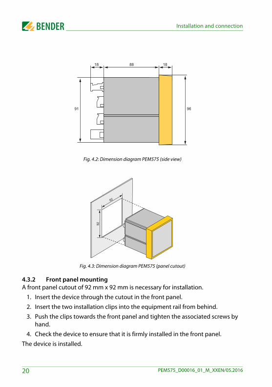
Fig. 4.2: Dimension diagram PEM575 (side view)
Fig. 4.3: Dimension diagram PEM575 (panel cutout)
4.3.2 Front panel mountingA front panel cutout of 92 mm x 92 mm is necessary for installation.
1. Insert the device through the cutout in the front panel.
2. Insert the two installation clips into the equipment rail from behind.
3. Push the clips towards the front panel and tighten the associated screws by hand.
4. Check the device to ensure that it is firmly installed in the front panel.
The device is installed.
18 88
91
18
96
92
92
20 PEM575_D00016_01_M_XXEN/05.2016
Installation and connection
4.4 Connection of the device
4.4.1 Safety information
4.4.2 Back-up fusesBack-up fuse supply voltage: 6 AShort-circuit protection Protect the measuring inputs according to the requirements of the standards. (Recommendation: 2 A). A suitable isolation means must be provided. For details refer to the operating manuals of the measuring current transformers currently used.
4.4.3 Connection of measuring current transformersWhen connecting the measuring current transformers it is important to consider the requirements of DIN VDE 0100-557 (VDE 0100-557) – Low voltage installations - Part 5: Selection and erection of electrical equipment - Section 557: Auxiliary circuits.
4.5 Instructions for connection Connect the PEM575 to the supply voltage (terminals A1 and A2 resp. +/-). Con-
nect terminal " " to the protective conductor. Power protection by a 6 A fuse, quick response. If being supplied from an IT sys-
tem, both lines have to be protected by a fuse. Connection to the RS-485 bus is made via the terminals D+, D- and SH. Up to 32
devices can be connected to the bus. The maximum cable length for the bus con-nection of all devices is 1200 m.
Danger of electric shock! Follow the basic safety rules when working with electricity.Consider the data on the rated voltage and supply voltage as specifiedin the technical data!
If the supply voltage Us is supplied by an IT system, both lines are to beprotected.
DANGER
21PEM575_D00016_01_M_XXEN/05.2016
Installation and connection
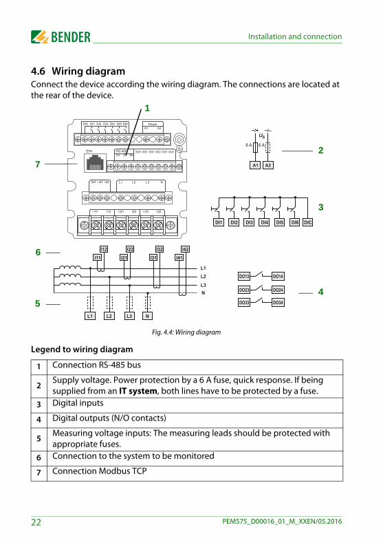
4.6 Wiring diagramConnect the device according the wiring diagram. The connections are located at the rear of the device.
Fig. 4.4: Wiring diagram
Legend to wiring diagram
1 Connection RS-485 bus
2Supply voltage. Power protection by a 6 A fuse, quick response. If being supplied from an IT system, both lines have to be protected by a fuse.
3 Digital inputs
4 Digital outputs (N/O contacts)
5Measuring voltage inputs: The measuring leads should be protected with appropriate fuses.
6 Connection to the system to be monitored
7 Connection Modbus TCP
D+
DIC DI1 DI2 DI3 DI4 DI5 DI6A1 A2
Power
RS-485ETHD- SH
• l11
• l41
l12
l42SH
l22 l32
L1 L2 L3 N
• l21 • l31
DO34 DO33 DO24 DO23 DO14 DO13
L1
I11I12
I21I22
I31I32
I41I42
L2L3N
DI1 DICDI5 DI6DI2 DI3 DI4
US
DO13 DO14
DO23 DO24
DO33 DO34
L1 L2 L3 N
2
3
4
7
5
6
1
22 PEM575_D00016_01_M_XXEN/05.2016
Installation and connection
4.7 Connection diagram voltage inputs
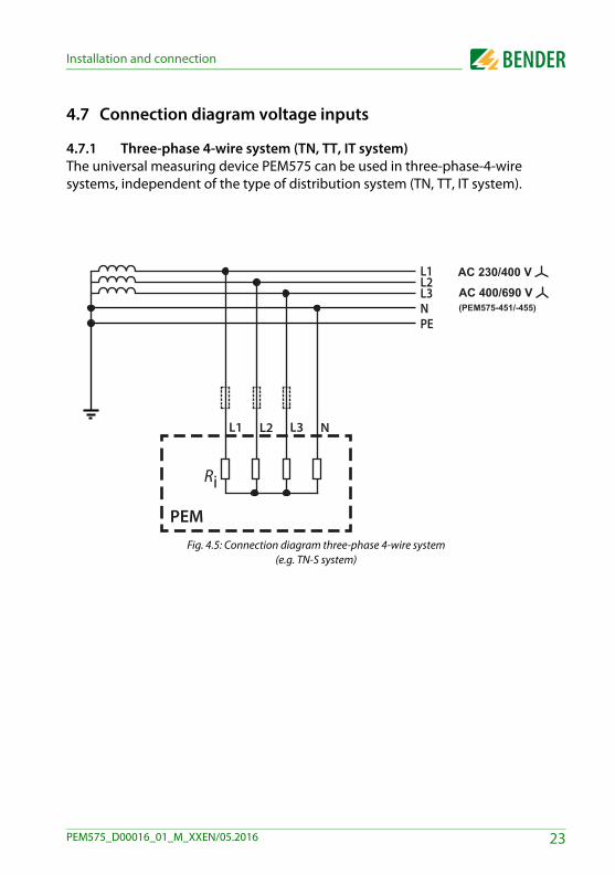
4.7.1 Three-phase 4-wire system (TN, TT, IT system)The universal measuring device PEM575 can be used in three-phase-4-wire systems, independent of the type of distribution system (TN, TT, IT system).
Fig. 4.5: Connection diagram three-phase 4-wire system(e.g. TN-S system)
L1 L2 L3 N
PEM
Ri
AC 230/400 V
AC 400/690 V(PEM575-451/-455)
23PEM575_D00016_01_M_XXEN/05.2016
Installation and connection
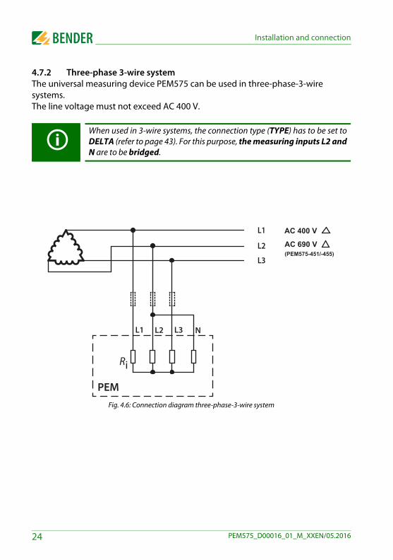
4.7.2 Three-phase 3-wire systemThe universal measuring device PEM575 can be used in three-phase-3-wire systems. The line voltage must not exceed AC 400 V.
Fig. 4.6: Connection diagram three-phase-3-wire system
When used in 3-wire systems, the connection type (TYPE) has to be set toDELTA (refer to page 43). For this purpose, the measuring inputs L2 andN are to be bridged.
L1 L2 L3
PEM
Ri
AC 400 V
N
AC 690 V(PEM575-451/-455)
24 PEM575_D00016_01_M_XXEN/05.2016
Installation and connection
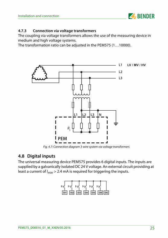
4.7.3 Connection via voltage transformersThe coupling via voltage transformers allows the use of the measuring device in medium and high voltage systems. The transformation ratio can be adjusted in the PEM575 (1…10000).
Fig. 4.7: Connection diagram 3-wire system via voltage transformers
4.8 Digital inputs The universal measuring device PEM575 provides 6 digital inputs. The inputs are supplied by a galvanically isolated DC 24 V voltage. An external circuit providing at least a current of Imin > 2.4 mA is required for triggering the inputs.
L1 L2 L3 N
PEM
Ri
LV / MV / HV
DI1 DICDI5 DI6DI2 DI3 DI4
25PEM575_D00016_01_M_XXEN/05.2016
Installation and connection
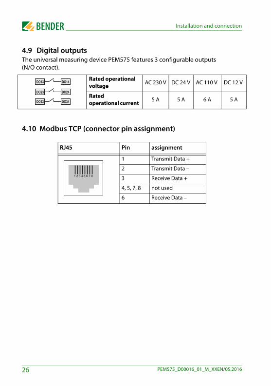
4.9 Digital outputsThe universal measuring device PEM575 features 3 configurable outputs (N/O contact).
4.10 Modbus TCP (connector pin assignment)
Rated operational voltage
AC 230 V DC 24 V AC 110 V DC 12 V
Ratedoperational current
5 A 5 A 6 A 5 A
RJ45 Pin assignment
1 Transmit Data +
2 Transmit Data –
3 Receive Data +
4, 5, 7, 8 not used
6 Receive Data –
DO13 DO14
DO23 DO24
DO33 DO34
1 2 3 4 5 6 7 8
26 PEM575_D00016_01_M_XXEN/05.2016
5. Commissioning
5.1 Check proper connectionObserve the relevant standards and regulations that have to be observed for installation and connection as well as the operating manual of the respective device.
5.2 Before switching onBefore switching on think carefully about these questions:
1. Does the connected supply voltage correspond to the nameplates' informa-tion?
2. Are you sure that the nominal insulation voltage of the measuring current transformer has not been exceeded?
3. Does the measuring current transformer's maximum current correspond to the nameplate information of the connected device?
5.3 Switching onAfter switching on, proceed as follows:
1. Connect the supply voltage.
2. Set the bus address/IP address.
3. Set the CT transformation ratio (for each channel).
4. Change the measuring current transformer's counting direction, if required.
5. Set the nominal voltage (line-to-line voltage ULL).
6. Select wye connection or delta connection.
5.4 SystemThe universal measuring device PEM575 can be programmed and queried via Modbus RTU. For details refer to „chapter 10. Modbus Register Map“ or the Internet www.modbus.org.
27PEM575_D00016_01_M_XXEN/05.2016

Commissioning
In addition, it is possible to integrate the device into Bender's own BMS (Bender measuring device interface) bus protocol via additional communication modules. In this way, communication with (already existing) Bender devices for device parameterisation and visualisation of measured values and alarms can be achieved.
Help and examples of system integration can be found on the Bender homepage www.bender.de or you can contact our Bender Service for personal advice (see „chapter 1.2 Technical support: Service and support“).
28 PEM575_D00016_01_M_XXEN/05.2016
6. Operation
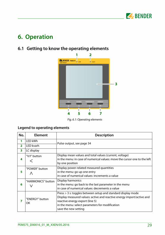
6.1 Getting to know the operating elements
Fig. 6.1: Operating elements
Legend to operating elements
No. Element Description1 LED kWh
Pulse output, see page 342 LED kvarh
3 LC display
4"V/I" button
Display mean values and total values (current, voltage)in the menu: in case of numerical values: move the cursor one to the left by one position
5"POWER" button
Display power-related measured quantitiesin the menu: go up one entryin case of numerical values: increments a value
6"HARMONICS" button
Display harmonicsin the menu: go back to the last parameter in the menuin case of numerical values: decrements a value
7"ENERGY" buttonOK
Press > 3 s: toggles between setup and standard display modeDisplay measured values: active and reactive energy import/active and reactive energy export (line 5)in the menu: select parameters for modificationsave the new setting
kvarhkWhPEM575
LINETRAXX®
V/I POWER HARMONICS ENERGY
OK
1 2
3
4 5 6 7
29PEM575_D00016_01_M_XXEN/05.2016
Operation
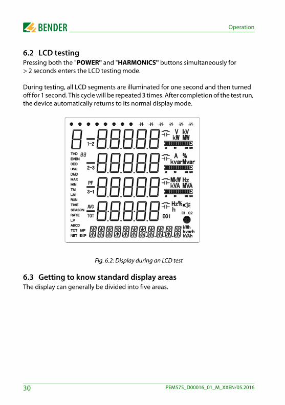
6.2 LCD testing Pressing both the "POWER" and "HARMONICS" buttons simultaneously for > 2 seconds enters the LCD testing mode.
During testing, all LCD segments are illuminated for one second and then turned off for 1 second. This cycle will be repeated 3 times. After completion of the test run, the device automatically returns to its normal display mode.
Fig. 6.2: Display during an LCD test
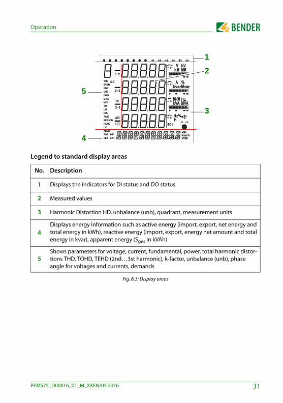
6.3 Getting to know standard display areasThe display can generally be divided into five areas.
30 PEM575_D00016_01_M_XXEN/05.2016
Operation
Legend to standard display areas
Fig. 6.3: Display areas
No. Description
1 Displays the indicators for DI status and DO status
2 Measured values
3 Harmonic Distortion HD, unbalance (unb), quadrant, measurement units
4Displays energy information such as active energy (import, export, net energy and total energy in kWh), reactive energy (import, export, energy net amount and total energy in kvar), apparent energy (Sges in kVAh)
5Shows parameters for voltage, current, fundamental, power, total harmonic distor-tions THD, TOHD, TEHD (2nd…3st harmonic), k-factor, unbalance (unb), phase angle for voltages and currents, demands
12
3
4
5
31PEM575_D00016_01_M_XXEN/05.2016
Operation
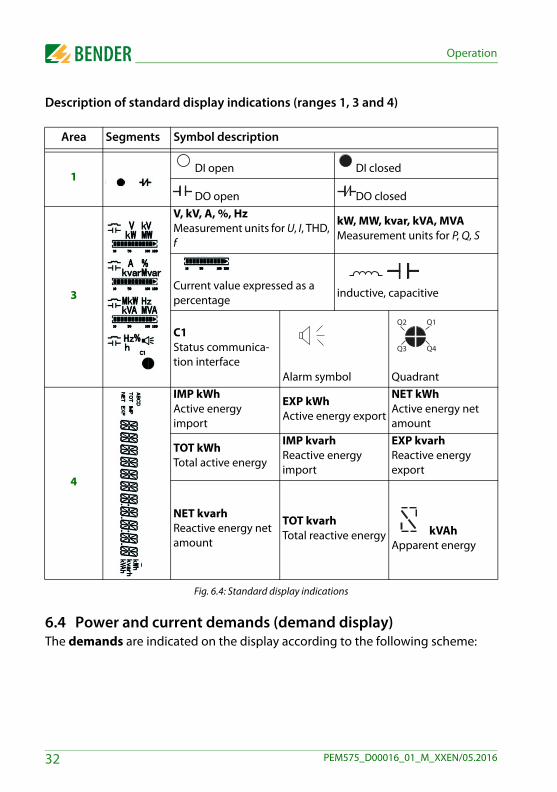
Description of standard display indications (ranges 1, 3 and 4)
Fig. 6.4: Standard display indications
6.4 Power and current demands (demand display)The demands are indicated on the display according to the following scheme:
Area Segments Symbol description
1 DI open DI closed
DO open DO closed
3
V, kV, A, %, HzMeasurement units for U, I, THD, f
kW, MW, kvar, kVA, MVAMeasurement units for P, Q, S
Current value expressed as a percentage
inductive, capacitive
C1Status communica-tion interface
Alarm symbol Quadrant
4
IMP kWhActive energy import
EXP kWhActive energy export
NET kWhActive energy net amount
TOT kWhTotal active energy
IMP kvarhReactive energy import
EXP kvarhReactive energy export
NET kvarhReactive energy net amount
TOT kvarhTotal reactive energy kVAh
Apparent energy
Q1
Q4Q3
Q2
32 PEM575_D00016_01_M_XXEN/05.2016
Operation
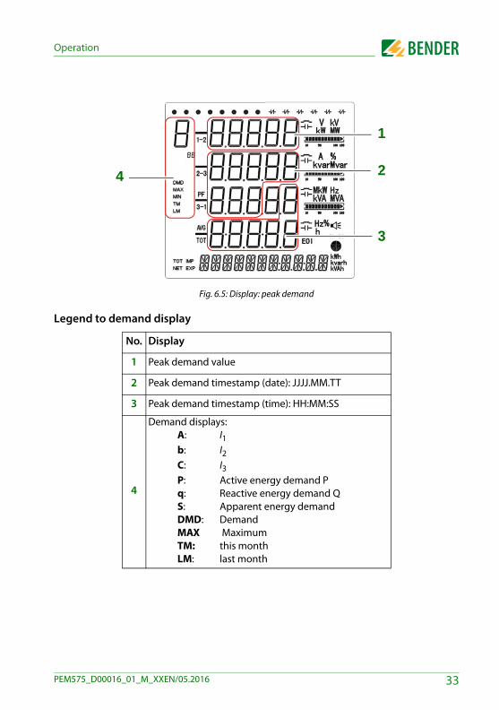
Fig. 6.5: Display: peak demand
Legend to demand display
No. Display
1 Peak demand value
2 Peak demand timestamp (date): JJJJ.MM.TT
3 Peak demand timestamp (time): HH:MM:SS
4
Demand displays: A: I1b: I2C: I3P: Active energy demand P q: Reactive energy demand Q S: Apparent energy demandDMD: DemandMAX MaximumTM: this monthLM: last month
1
2
3
4
33PEM575_D00016_01_M_XXEN/05.2016
Operation
6.5 LED indicationThe universal measuring device features two red LEDs on its front panel: kWh and kvarh.The two LED indicators are used for the indication of kWh and kvar, if the EN PULSE function is enabled. The setting can be carried out in the setup menu using the buttons on the front or via the communications interface..The LEDs flash each time a certain amount of energy is reached (1 kWh resp.1 kvarh). The amount of energy displayed corresponds to the amount of energy measured by the measuring device. In order to determine the actual amount of energy, the flashing frequency can be calculated from the CT ratio and the pulse constant.
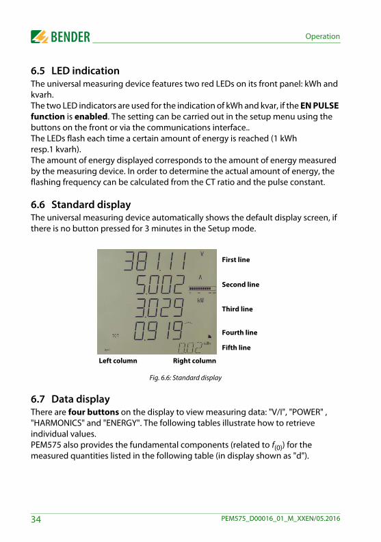
6.6 Standard displayThe universal measuring device automatically shows the default display screen, if there is no button pressed for 3 minutes in the Setup mode.
Fig. 6.6: Standard display
6.7 Data displayThere are four buttons on the display to view measuring data: "V/I", "POWER" , "HARMONICS" and "ENERGY". The following tables illustrate how to retrieve individual values. PEM575 also provides the fundamental components (related to f(0)) for the measured quantities listed in the following table (in display shown as "d").
First line
Second line
Third line
Fourth line
Fifth line
Right columnLeft column
34 PEM575_D00016_01_M_XXEN/05.2016
Operation
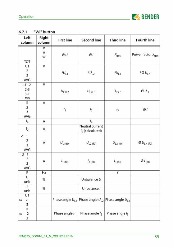
6.7.1 "V/I" buttonLeft
columnRight
column First line Second line Third line Fourth line
TOT
VAW
Ø U Ø I Pges Power factor λges
U123
AVG
V
*UL1 *UL2 *UL3 *Ø ULN
U1-22-33-1AVG
V
UL1L2 UL2L3 UL3L1 Ø ULL
I123
AVG
A
I1 I2 I3 Ø I
I4 A I4
I0 ANeutral current I0 (calculated)
d 1 23
AVG
V UL1(f0) UL2 (f0) UL3 (f0) Ø ULN (f0)
d 1 23
AVG
A I1 (f0) I2 (f0) I3 (f0) Ø I (f0)
F Hz fU
unb% Unbalance U
Iunb
% Unbalance I
U1PA 2
3Phase angle UL1 Phase angle UL2 Phase angle UL3
I1PA 2
3Phase angle I1 Phase angle I2 Phase angle I3
35PEM575_D00016_01_M_XXEN/05.2016
Operation
Tab. 6.1: Display screens via the "V/I" button
Note table 6.1: * When the wiring mode is "DELTA", the display will be bypassed and does not appear.
I1DMD 2
3A Demand I1 Demand I2 Demand I3 Ø Demand I
DMD I4 A Demand I4A
DMD MAX TM
APeak demand I1
this monthJJJJ.MM.TT hh:mm:ss
bDMD MAX TM
APeak demand I2
this month JJJJ.MM.TT hh:mm:ss
CDMD MAX TM
APeak demand I3
this monthJJJJ.MM.TT hh:mm:ss
ADMD MAX LM
APeak demand I1
last monthJJJJ.MM.TT hh:mm:ss
bDMD MAX LM
APeak demand I2
last monthJJJJ.MM.TT hh:mm:ss
CDMD MAX LM
APeak demand I3
last monthJJJJ.MM.TT hh:mm:ss
Left column
Right column First line Second line Third line Fourth line
36 PEM575_D00016_01_M_XXEN/05.2016
Operation
6.7.2 "POWER"button
Left column
Right column First line Second line Third line Fourth line
* P123
TOT
W PL1* PL2
* PL3* Pges
*q123
TOT
var QL1* QL2
* QL3* Qges
*S123
TOT
VA SL1* SL2
* SL3* Sges
*PF123
TOT
λL1* λL2
* λL3* λges
d123
TOT
W PL1 (f0) PL2 (f0) PL3 (f0) Pges (f0)
d123
TOT
var QL1 (f0) QL2 (f0) QL3 (f0) Qges (f0)
d123
TOT
VA SL1 (f0) SL2 (f0) SL3 (f0) Sges (f0)
*dPF123
TOT
Displacement factor cos (φ)L1 f(0)
*Displacement
factor cos (φ)L2 f(0)*
Displacement factor cos (φ)L3 f(0)
*
Displace-ment factor cos (φ) f(0)
TOTW
varVA
Pges Qges Sges λges
37PEM575_D00016_01_M_XXEN/05.2016
Operation
Tab. 6.2: Display possibilities via the "POWER" button
Note table 6.2: * When the wiring mode is "DELTA", the display will be bypassed and does not appear.
dTOT
WvarVA
Pges (f0) Qges (f0) Sges (f0) λges (f0)
DMDTOT
WvarVA
Demand Pges Demand Qges Demand SgesDemand
λges
PDMDTOT
WvarVA
Predicted demand Pges
Predicted demand Qges
Predicted demand Sges
Predicted demand
λges
PDMDMAXTM
kWPeak demand P
this monthYYYY.MM.DD hh:mm:ss
qDMDMAXTM
kvarPeak demand Q
this monthYYYY.MM.DD hh:mm:ss
SDMDMAXTM
kVAPeak demand S
this monthYYYY.MM.DD hh:mm:ss
PDMDMAXLM
kWPeak demand P
last monthYYYY.MM.DD hh:mm:ss
QDMDMAXLM
kvarPeak demand Q
last monthYYYY.MM.DD hh:mm:ss
SDMDMAXLM
kVAPeak demand S
last monthYYYY.MM.DD hh:mm:ss
Left column
Right column First line Second line Third line Fourth line
38 PEM575_D00016_01_M_XXEN/05.2016
Operation
6.7.3 "HARMONICS" button
Left column
Right column First line Second line Third line Fourth line
THD U123
AVG
% THDUL1 THDUL2 THDUL3 Ø THDULN
THD I123
AVG
% THDI1 THDI2 THDI3 Ø THDI
123
k-factor I1 k-factor I2 k-factor I3
UTHDEven
% TEHDUL1 TEHDUL2 TEHDUL3 Ø TEHDULN
ITHDEven
% TEHDI1 TEHDI2 TEHDI3 Ø TEHDI
UTHDODD
% TOHDUL1 TOHDUL2 TOHDUL3 Ø TOHDULN
ITHDODD
% TOHDI1 TOHDI2 TOHDI3 Ø TOHDI
HD2 U1
23
AVG
% 2nd 2nd 2nd Ø 2nd
HD2 I123
AVG
% 2nd 2nd 2nd harmonic I3 Ø 2nd harmonic I
HD3 U123
AVG
% 3rd 3rd 3rd Ø 3rd
…
39PEM575_D00016_01_M_XXEN/05.2016
Operation
Tab. 6.3: Display screens via the "HARMONICS" button
Note table 6.3: * The harmonics 32…63 can only be queried via the communication interface.
6.7.4 "ENERGY" buttonThe "Energy" button switches through the displays of the fifth line:
Tab. 6.4: Display screens via the "ENERGY" button
HD31 U1
23
AVG
% 31st 31st 31st Ø 31st
*HD31 I123
AVG
% 31st 31st 31st harmonic I3 Ø 31st harmonic I
Left column Right column Value
IMP kWh Active energy import
EXP kWh Active energy export
NET kWh Active energy net amount
TOT kWh Total active energy
IMP kvarh Reactive energy import
EXP kvarh Reactive energy export
NET kvarh Reactive energy net amount
TOT kvarh Total reactive energy
S kVAh Apparent energy
Left column
Right column First line Second line Third line Fourth line
40 PEM575_D00016_01_M_XXEN/05.2016
Operation
6.8 Setup configuration via the front panelPressing the "ENERGY" button for more than 3 seconds enters the Setup configuration mode. Upon completion, pressing the "ENERGY" button for more than 3 seconds returns to the data display mode.
6.8.1 Setup: Function of buttonsThe meanings of the buttons in the Setup mode are indicated below each button:
"V / I": arrow button " " moves the cursor to the left by one position if the parameter being changed is a numerical value
"POWER": arrow button " " advances to the next parameter in the menu or increments a numerical value
"HARMONICS": arrow button " " goes back to the last parameter in the menu or decrements a numerical value
"ENERGY": OK to confirm the value entered
A correct password must be entered before parameter changes areallowe (factory default password is 0).
41PEM575_D00016_01_M_XXEN/05.2016
Operation
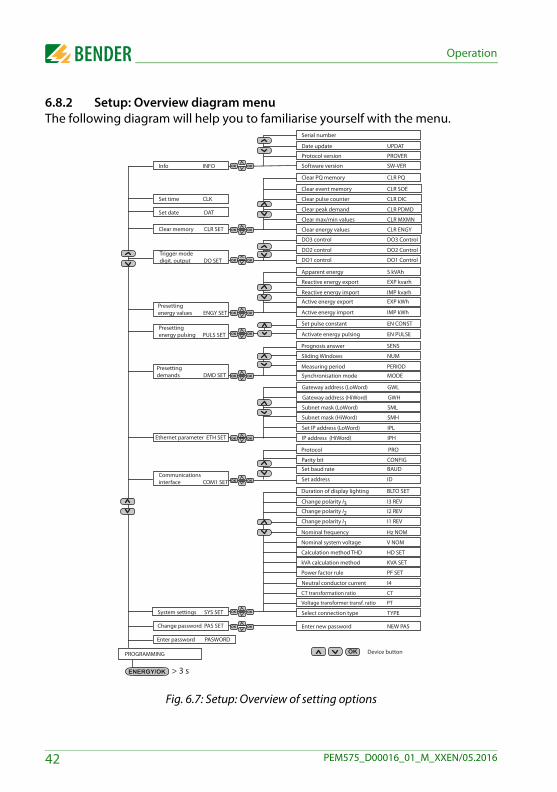
6.8.2 Setup: Overview diagram menuThe following diagram will help you to familiarise yourself with the menu.
Fig. 6.7: Setup: Overview of setting options
OK
OKOK
OKOK
OKOK
OKOK
OKOK
OKOK
OKOK
OKOK
OKOK
OKOK
PROGRAMMING
Enter password PASWORD
Change password PAS SET
Set date DAT
Presetting
demands DMD SET
Presetting
energy values ENGY SET
Set time CLK
Trigger mode
digit. output DO SET
Info INFO
Device button
System settings SYS SET
Clear memory CLR SET
Communications
interface COM1 SET
Presetting
energy pulsing PULS SET
> 3 sENERGY/OK
Activate energy pulsing EN PULSE
Enter new password NEW PAS
Select connection type TYPE
Voltage transformer transf. ratio PT
Set baud rate BAUD
CT transformation ratio CT
Set pulse constant EN CONST
Clear energy values CLR ENGY
Clear max/min values CLR MXMN
Clear peak demand CLR PDMD
Reactive energy import IMP kvarh
Active energy export EXP kWh
Active energy import IMP kWh
Reactive energy export EXP kvarh
Apparent energy S kVAh
Serial number
Date update UPDAT
Protocol version PROVER
Software version SW-VER
Set address ID
Parity bit CONFIG
kVA calculation method KVA SET
Neutral conductor current I4
Sliding Windows NUM
Measuring period PERIOD
DO1 control DO1 Control
Change polarity I3 I3 REV
Change polarity I2 I2 REV
Change polarity I1 I1 REV
DO2 control DO2 Control
Clear pulse counter CLR DIC
Clear event memory CLR SOE
Duration of display lighting BLTO SET
Power factor rule PF SET
Calculation method THD HD SET
Nominal system voltage V NOM
Nominal frequency Hz NOM
Protocol PRO
Ethernet parameter ETH SET
Set IP address (LoWord) IPL
IP address (HiWord) IPH
Subnet mask (HiWord) SMH
Subnet mask (LoWord) SML
Gateway address (HiWord) GWH
Gateway address (LoWord) GWL
Synchronisation mode MODE
Prognosis answer SENS
DO3 control DO3 Control
Clear PQ memory CLR PQ
42 PEM575_D00016_01_M_XXEN/05.2016
Operation
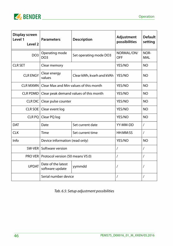
6.9 Setup: adjustment possibilitiesThe table illustrates the display screens, their meaning and the adjustment possibilities.
Display screenLevel 1
Level 2Parameters Description Adjustment
possibilitiesDefaultsetting
PROGRAMMING Setup mode
PASWORD Password Enter password / 0
PAS SET Change password? YES/NO NO
NEW PAS New password Enter new password 0000…9999 0
SYS SET System settings YES/NO NO
TYPE Wiring mode Select wiring modeWYE/DELTA/DEMO
WYE
PTVoltage transfor-mer
Select voltage transfor-mer transformation ratio
1…10,000 1
CTMeasuring current transformers
Select CT transformation ratio
1…30,000 (1 A)1…6,000 (5 A)
1
I4 Neutral currentSelect CT transformation ratio for I4
1…10,000 1
PF SET Power factor rule Power factor rule* IEC/IEEE/-IEEE IEC
KVA SET S calculation method ** V/S V
HD SET Harmonic distortion calculation method *** FUND/RMS FUND
V NOM Nominal voltage Unom (equals ULL) 100…700 (V) 100
Hz NOM Nominal frequency fnom 50/60 (Hz) 50
I1 REV I1 CTReverse phase I1 CT polarity
YES/NO NO
43PEM575_D00016_01_M_XXEN/05.2016

Operation
I2 REV I2 CTReverse phase I2 CT polarity
YES/NO NO
I3 REV I3 CTReverse phase I3 CT polarity
YES/NO NO
BLTO SET Display backlight Backlight timeout0…60 (minutes)
3
COM 1 SET Configure communications interface YES/NO NO
ID1Measuring device address
Set address for measuring device
1…247 100
BAUD1 Baud rate Set baud rate1200/2400/4800/9600/19200 bps
9600
CONFIG1 Parity bit Parity bit configuration8N2/8O1/8E1/8N1/8O2/8E2
8E1
PRO ProtocolMODBUS/EGATE
Modbus
ETH SET Configure Ethernet parameters YES/NO NO
IPH IP address (HiWord) 192.168
IPL IP address (LoWord) 8.97
SMH Subnet mask (HiWord) 255.255
SML Subnet mask (LoWord) 255.0
GWH Gateway address (HiWord) 192.168
GWL Gateway address (LoWord) 8.1
DMD SET Demand measurement on/off YES/NO NO
MODE Synchronisation mode demand SLD/SYNC SLD
Display screenLevel 1
Level 2Parameters Description Adjustment
possibilitiesDefaultsetting
44 PEM575_D00016_01_M_XXEN/05.2016
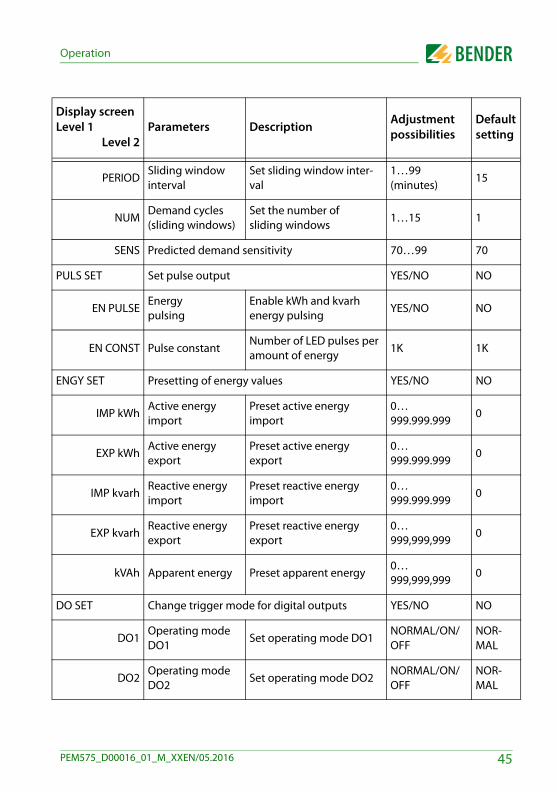
Operation
PERIODSliding window interval
Set sliding window inter-val
1…99 (minutes)
15
NUMDemand cycles (sliding windows)
Set the number ofsliding windows
1…15 1
SENS Predicted demand sensitivity 70…99 70
PULS SET Set pulse output YES/NO NO
EN PULSEEnergy pulsing
Enable kWh and kvarh energy pulsing
YES/NO NO
EN CONST Pulse constantNumber of LED pulses per amount of energy
1K 1K
ENGY SET Presetting of energy values YES/NO NO
IMP kWhActive energy import
Preset active energy import
0… 999.999.999
0
EXP kWhActive energy export
Preset active energy export
0… 999.999.999
0
IMP kvarhReactive energy import
Preset reactive energy import
0… 999.999.999
0
EXP kvarhReactive energy export
Preset reactive energy export
0… 999,999,999
0
kVAh Apparent energy Preset apparent energy0… 999,999,999
0
DO SET Change trigger mode for digital outputs YES/NO NO
DO1Operating mode DO1
Set operating mode DO1NORMAL/ON/OFF
NOR-MAL
DO2Operating mode DO2
Set operating mode DO2NORMAL/ON/OFF
NOR-MAL
Display screenLevel 1
Level 2Parameters Description Adjustment
possibilitiesDefaultsetting
45PEM575_D00016_01_M_XXEN/05.2016
Operation
Tab. 6.5: Setup adjustment possibilities
DO3Operating mode DO3
Set operating mode DO3NORMAL/ON/OFF
NOR-MAL
CLR SET Clear memory YES/NO NO
CLR ENGYClear energy values
Clear kWh, kvarh and kVAh YES/NO NO
CLR MXMN Clear Max and Min values of this month YES/NO NO
CLR PDMD Clear peak demand values of this month YES/NO NO
CLR DIC Clear pulse counter YES/NO NO
CLR SOE Clear event log YES/NO NO
CLR PQ Clear PQ log YES/NO NO
DAT Date Set current date YY-MM-DD /
CLK Time Set current time HH:MM:SS /
Info Device information (read only) YES/NO NO
SW-VER Software version / /
PRO VER Protocol version (50 means V5.0) / /
UPDATDate of the latest software update
yymmdd / /
Serial number device / /
Display screenLevel 1
Level 2Parameters Description Adjustment
possibilitiesDefaultsetting
46 PEM575_D00016_01_M_XXEN/05.2016

Operation
rt
Explanatory notes table 6.5
*Power factor λ rules
"IEEE" is the same as "-IEEE" but with the opposite sign.
**There are two ways to calculate the apparent power S:
Choose the calculation method: V = Vector methodS = Scalar method
Quadrant 3
Power factor (-)
Active power export (-)
Reactive power export (-)
Quadrant 4
Power factor (+)
Active power import (+)
Reactive power export (-)
Quadrant 1
Power factor (+)
Active power import (+)
Reactive power import (+)
Quadrant 2
Power factor (-)
Active power export (-)
Reactive power import (+)
IEC
Reactive power import
Active power import
Quadrant 3
Power factor (-)
Active power export (-)
Reactive power export (-)
Quadrant 4
Power factor (+)
Active power import (+)
Reactive power export (-)
Quadrant 1
Power factor (-)
Active power export (+)
Reactive power import (+)
Quadrant 2
Power factor (+)
Active power export (-)
Reactive power import (+)
IEEE
Reactive power import
Active power impo
Sges = P
ges2 + Q
ges
2
Vector method V: Scalar method S:
Sges = SL1 + SL2 + SL3
47PEM575_D00016_01_M_XXEN/05.2016
Operation
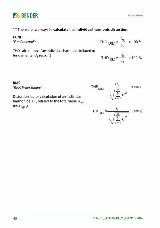
***There are two ways to calculate the individual harmonic distortion:
FUND"Fundamental":
THD calculation of an individual harmonic (related to fundamental U1 resp. I1)
RMS "Root Mean Square":
Distortion factor calculation of an individual harmonic (THF, related to the total value Uges resp. Iges)
THD U(k) = UkU1
x 100 %
THD I(k) = IkI1
x 100 %
Uk
Uk Σ∞
k = 1
THFU(k) = 2
x 100 %
Ik
Ik Σ∞
k = 1
THFI(k) = 2
x 100 %
48 PEM575_D00016_01_M_XXEN/05.2016
Operation
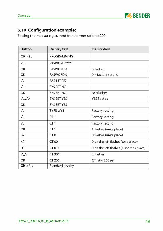
6.10 Configuration example:Setting the measuring current transformer ratio to 200
Button Display text Description
OK > 3 s PROGRAMMING
PASWORD ****
OK PASWORD 0 0 flashes
OK PASWORD 0 0 = factory setting
PAS SET NO
SYS SET NO
OK SYS SET NO NO flashes
or SYS SET YES YES flashes
OK SYS SET YES
TYPE WYE Factory setting
PT 1 Factory setting
CT 1 Factory setting
OK CT 1 1 flashes (units place)
CT 0 0 flashes (units place)
CT 00 0 on the left flashes (tens place)
CT 0 0 0 on the left flashes (hundreds place)
CT 200 2 flashes
OK CT 200 CT ratio 200 set
OK > 3 s Standard display
49PEM575_D00016_01_M_XXEN/05.2016

Operation
50 PEM575_D00016_01_M_XXEN/05.2016
7. Application/inputs and outputs
7.1 Digital inputs (DI)The device features six digital inputs which are internally operated with DC 24 V.Digital inputs are typically used for monitoring external statuses. The real-time statuses of the digital inputs are available on the front panel LC display as well as through connected system components. Changes in external statuses are stored as events in the SOE log in 1 ms resolution. One of the digital inputs can be programmed to receive pulses for the synchronisation of the demand measurement. The setting is to be carried out via register 6021 (page 117).Digital inputs can also be used as external time synchronisation pulse (see page 84).
7.2 Digital outputs (DO)The device features three digital outputs. Digital outputs are typically used for setpoint alarming, load control or remote control applications.Examples:
1. Manually operated from the front panel (Chapter 6.8 Setup configuration via the front panel)
2. Operation via communications interface (Chapter 10.19 DOx output control).
3. Control setpoints: Control actions in response to a specific condition (Chapter 7.6 Setpoints)
4. Digital outputs triggered by logic modules(Chapter 10.12 Logic module).
5. Triggered by undervoltage or overvoltage(Chapter 9.4 Undervoltage/overvoltage setpoint (sag/swell setpoint)).
6. Triggered by transient events(Chapter 9.5 Transient events setpoint).
7. Control via digital inputs
Priority: Front panel control has a higher priority and overwrites the other applications.
51PEM575_D00016_01_M_XXEN/05.2016
Application/inputs and outputs
For a general alarm, all setpoints can be programmed to control the same digital output. However, if the user intends to generate a control signal in response to a specific setpoint condition, each DO may be controlled by only one source.
7.3 Energy pulsing outputThe two LED pulse outputs are used for kWh and kvarh indication, if the function EN PULSE is enabled. Energy pulsing can be enabled from the front panel through the EN Pulse setup parameter or via the communications interface.The LEDs flash each time a certain amount of energy is reached (1 kWh resp. 1 kvarh). In order to relate the flashing frequency to the amount of energy, the transformation ratios and the pulse constant have to be considered.
7.4 Power and energy
7.4.1 Basic measurementsThe PEM575 provides the following basic measurements with a 1 second update rate: three-phase voltages three-phase currents three-phase power three-phase power factors λ Neutral current Frequency Energy import and export Voltage and current phase angles
Note: VT = voltage transformer
CT = measuring current transformer
Pulses per kWh = Pulse constant
ratio VT x ratio CT
Amount of energyper pulse Pulse constant
ratio VT x ratio CT=
52 PEM575_D00016_01_M_XXEN/05.2016
Application/inputs and outputs
7.4.2 High-speed measurementsIn addition to the basic measurements, the PEM575 provides the following high-speed measurements: three-phase voltages (10 ms) three-phase currents (20 ms) three-phase power (20 ms) three-phase power factors λ (20 ms) Neutral current (20 ms)
7.4.3 Voltage and current phase anglesPhase angle analysis is used to identify the angle relationship between the voltages and currents of the three line conductors.
7.4.4 EnergyBasic energy parameters include active energy (import, export, net energy and total energy in kWh) reactive energy (import, export, net energy and total energy in kvarh) as well as
reactive energy related to the quadrants Q1…Q4 apparent energy (Sges in kVAh)The maximum value to be displayed is ± 999,999,999,99. When the maximum value is reached, the register will automatically roll over to zero. The counter value can be edited via software or through the front panel, password required.
7.5 Demand DMDThe demand is defined as an average consumption value over a fixed demand period. PEM575 supports the "Sliding windows" demand calculation; in addition to the demand period also the demand cycles, which are to be considered, are specified here. The following parameters can be set: Synchronisation mode
– SLD internally synchronised to the PEM's clock– SYNC DI externally synchronised to a digital input that has been program-
med as a demand synchronisation input (DI function = SYNC DI) Demand cycles (1…15)
53PEM575_D00016_01_M_XXEN/05.2016
Application/inputs and outputs
Demand period (1…99 min)Example of a total demand period:
Demand cycles: 3Demand period: 20 minTotal demand period: 3 x 20 min = 60 min
Predicted demand sensitivity SENS (70…99)
Values are determined for present demand and predicted demand Voltages (U1, U2, U3, ØULN, UL1L2, UL2L3, UL3L1, ØULL) Currents (I1, I2, I3, Ø I, I4) Active power P (P1, P2, P3, Pges) Apparent power S (S1, S2, S3, Sges) Reactive power Q (Q1, Q2, Q3, Qges) Power factor λ (λ1, λ2, λ3, λges) Frequency Voltage unbalance Current unbalance Total harmonic distortion, voltage
(THDU1, THDU2, THDU3) Total harmonic distortion, current
(THDI1, THDI2, THDI3)
The demand period can be set using the buttons on the front panel or via the communications interface. The following options are available:1, 2, 3, 5, 10, 15, 30, 60 minutesIn addition to the demand period also the demand cycles (sliding window) between 1 and 15 are to be specified.
During the total demand period (duration multiplied by the number), the consumption resp. the imported power is measured. Then the average demand value is indicated on the display and output via the communications interface. The maximum demand value (peak demand) determined over the whole recording period will be saved and displayed. The peak demand can be reset manually. Setting possibilities: Chapter 6.9 Setup: adjustment possibilities.
54 PEM575_D00016_01_M_XXEN/05.2016

Application/inputs and outputs
7.5.1 Max/Min values per demand periodThe PEM575 records the min and max values of the following measurements for each demand period three-phase voltages three-phase currents three-phase frequencies three-phase power three-phase power factors λ Voltage unbalance Current unbalance Total harmonic distortion, voltage (THDU) Total harmonic distortion, current (THDI)All recorded measuring values can be accessed via the communications interface.
7.6 SetpointsThe PEM575 features 24 user-programmable control setpoints (registers 6600…6839) which provide extensive control by allowing a user to initiate an action in response to a specific condition. The alarm symbol at the right side of the LC display is lit if there are any active setpoints.
The first 16 setpoints (1…16) are standard setpoints, the other setpoints (17…24) are high-speed setpoints. Typical setpoint applications are alarming, fault location and power quality monitoring (PQ monitoring). Setpoints can be programmed via the communications interface. The following setup parameters are provided:
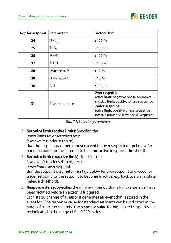
1. Setpoint type: Specifies the monitoring condition (over setpoint or under setpoint) or is disabled.
2. Setpoint parameters: Specifies the parameters to be monitored; for standard setpoints all parameters are available, for high-speed setpoints only the keys 1…14 apply.
55PEM575_D00016_01_M_XXEN/05.2016
Application/inputs and outputs
Setpoints
Key for setpoint Parameters Factor; Unit
1 ULN x 100; V
2 ULL x 100; V
3 I x 1000; A
4 I4 x 1000; A
5 Δ f x 100, Hz
6 Pges kW
7 Qges kvar
8 λ x 1,000
9 DI1Over setpointactive limit: DI= 1 (close)inactive limit: DI = 0 (open)
Under setpointactive limit: DI= 0 (open)inactive limit: DI = 1 (close)
10 DI2
11 DI3
12 DI4
13 DI5
14 DI6
15 Reserved
16 Demand Pges kW
17 Demand Qges kvar
18 Demand λ x 1,000
19 Predicted demand Pges kW
20 Predicted demand Qges kvar
21 Predicted demand λ x 1,000
22 THDU x 100, %
23 TOHDU x 100, %
56 PEM575_D00016_01_M_XXEN/05.2016
Application/inputs and outputs
Tab. 7.1: Setpoint parameters
3. Setpoint limit (active limit): Specifies the upper limits (over setpoint) resp. lower limits (under setpoint)that the setpoint parameter must exceed for over setpoint or go below for under setpoint for the setpoint to become active (response threshold).
4. Setpoint limit (inactive limit): Specifies thelower limits (under setpoint) resp. upper limits (over setpoint) that the setpoint parameter must go below for over setpoint or exceed for under setpoint for the setpoint to become inactive, e.g. back to normal state (release threshold).
5. Response delay: Specifies the minimum period that a limit value must have been violated before an action is triggered. Each status change of a setpoint generates an event that is stored in the event log. The response value for standard setpoints can be indicated in the range of 0…9.999 seconds. The response value for high-speed setpoints can be indicated in the range of 0…9.999 cycles.
24 TEHDU x 100, %
25 THDI x 100, %
26 TOHDI x 100, %
27 TEHDI x 100, %
28 Unbalance U x 10, %
29 Unbalance I x 10, %
30 Δ U x 100, %
31 Phase sequence
Over setpointactive limit: negative phase sequenceinactive limit: positive phase sequenceUnder setpointactive limit: positive phase sequenceinactive limit: negative phase sequence
Key for setpoint Parameters Factor; Unit
57PEM575_D00016_01_M_XXEN/05.2016
Application/inputs and outputs
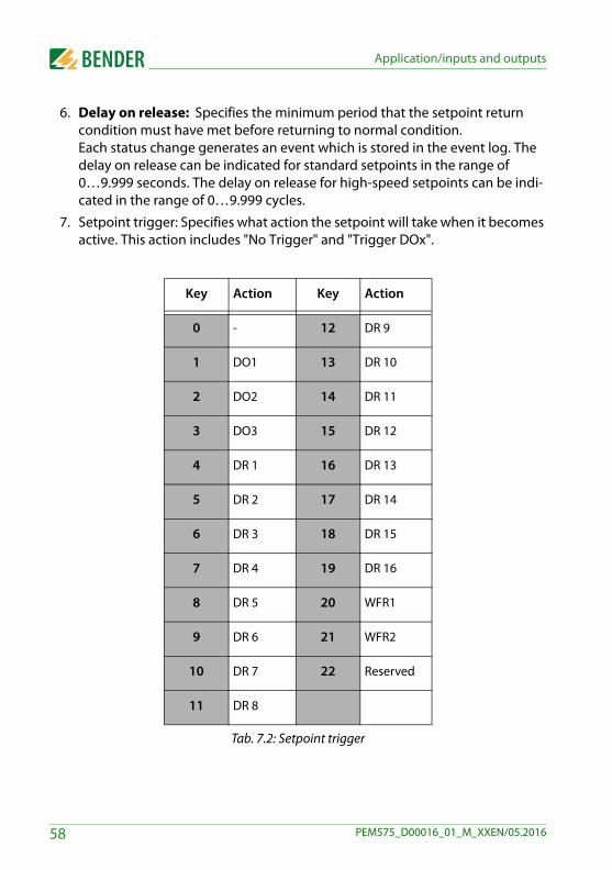
6. Delay on release: Specifies the minimum period that the setpoint return condition must have met before returning to normal condition. Each status change generates an event which is stored in the event log. The delay on release can be indicated for standard setpoints in the range of 0…9.999 seconds. The delay on release for high-speed setpoints can be indi-cated in the range of 0…9.999 cycles.
7. Setpoint trigger: Specifies what action the setpoint will take when it becomes active. This action includes "No Trigger" and "Trigger DOx".
Tab. 7.2: Setpoint trigger
Key Action Key Action
0 - 12 DR 9
1 DO1 13 DR 10
2 DO2 14 DR 11
3 DO3 15 DR 12
4 DR 1 16 DR 13
5 DR 2 17 DR 14
6 DR 3 18 DR 15
7 DR 4 19 DR 16
8 DR 5 20 WFR1
9 DR 6 21 WFR2
10 DR 7 22 Reserved
11 DR 8
58 PEM575_D00016_01_M_XXEN/05.2016
Application/inputs and outputs
7.7 Logic modulesThe PEM575 provides six programmable logic modules which perform AND, NAND, OR or NOR logical operations. Each logic module is capable of linking four different setpoint conditions with each other.
Logical expression =
{(source 1 [mode 1] source 2) [mode 2] source 3} [mode 3] source 4
The alarm symbol at the right side of the LC display appears when there are active logic modules. Logic modules are programmed via the communications interface.
Details about the applied registers and their data structure you will find on page 127.
The following setup parameters are provided:
1. Activating logic modules
2. Mode 1…3: Specifies the type of logical evaluation to be performed (AND, NAND, OR, NOR).
3. Source 1…4: Specifies the source inputs (table 10.30).
4. Trigger : Trigger 1 and Trigger 2 specify what action the logic module will take when it becomes active (table 10.31).
59PEM575_D00016_01_M_XXEN/05.2016

Application/inputs and outputs
60 PEM575_D00016_01_M_XXEN/05.2016
8. Logging
8.1 Peak demand logThe PEM575 stores the demand data of the last month and this month with timestamp for I1, I2, I3, Pges, Qges and Sges. All values can be accessed through the front panel buttons as well as the communications interface. Data for this month can be deleted through the front panel buttons as well as the communications interface.
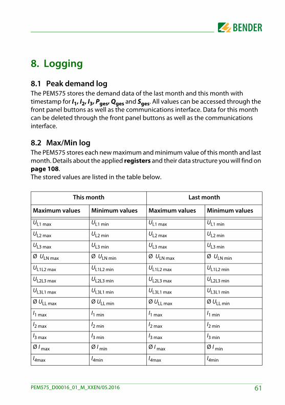
8.2 Max/Min logThe PEM575 stores each new maximum and minimum value of this month and last month. Details about the applied registers and their data structure you will find on page 108.The stored values are listed in the table below.
This month Last month
Maximum values Minimum values Maximum values Minimum values
UL1 max UL1 min UL1 max UL1 min
UL2 max UL2 min UL2 max UL2 min
UL3 max UL3 min UL3 max UL3 min
Ø ULN max Ø ULN min Ø ULN max Ø ULN min
UL1L2 max UL1L2 min UL1L2 max UL1L2 min
UL2L3 max UL2L3 min UL2L3 max UL2L3 min
UL3L1 max UL3L1 min UL3L1 max UL3L1 min
Ø ULL max Ø ULL min Ø ULL max Ø ULL min
I1 max I1 min I1 max I1 min
I2 max I2 min I2 max I2 min
I3 max I3 min I3 max I3 min
Ø I max Ø I min Ø I max Ø I min
I4max I4min I4max I4min
61PEM575_D00016_01_M_XXEN/05.2016
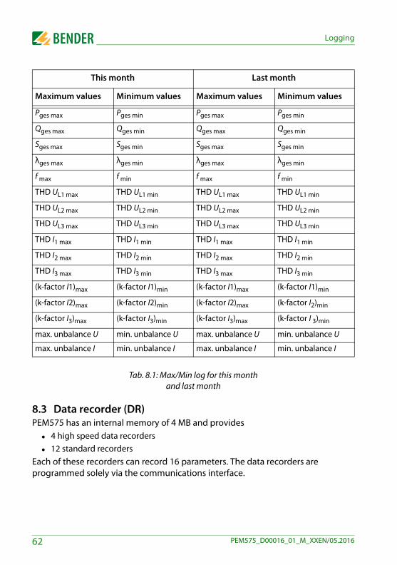
Logging
Tab. 8.1: Max/Min log for this month and last month
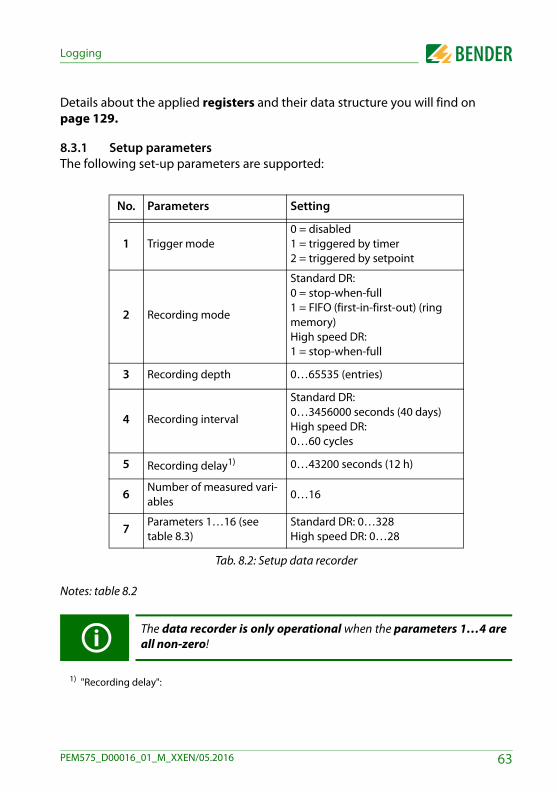
8.3 Data recorder (DR)PEM575 has an internal memory of 4 MB and provides 4 high speed data recorders 12 standard recorders Each of these recorders can record 16 parameters. The data recorders are programmed solely via the communications interface.
Pges max Pges min Pges max Pges min
Qges max Qges min Qges max Qges min
Sges max Sges min Sges max Sges min
λges max λges min λges max λges min
f max f min f max f min
THD UL1 max THD UL1 min THD UL1 max THD UL1 min
THD UL2 max THD UL2 min THD UL2 max THD UL2 min
THD UL3 max THD UL3 min THD UL3 max THD UL3 min
THD I1 max THD I1 min THD I1 max THD I1 min
THD I2 max THD I2 min THD I2 max THD I2 min
THD I3 max THD I3 min THD I3 max THD I3 min
(k-factor I1)max (k-factor I1)min (k-factor I1)max (k-factor I1)min
(k-factor I2)max (k-factor I2)min (k-factor I2)max (k-factor I2)min
(k-factor I3)max (k-factor I3)min (k-factor I3)max (k-factor I 3)min
max. unbalance U min. unbalance U max. unbalance U min. unbalance U
max. unbalance I min. unbalance I max. unbalance I min. unbalance I
This month Last month
Maximum values Minimum values Maximum values Minimum values
62 PEM575_D00016_01_M_XXEN/05.2016
Logging
Details about the applied registers and their data structure you will find on page 129.
8.3.1 Setup parametersThe following set-up parameters are supported:
Tab. 8.2: Setup data recorder
Notes: table 8.2
1) "Recording delay":
No. Parameters Setting
1 Trigger mode0 = disabled1 = triggered by timer2 = triggered by setpoint
2 Recording mode
Standard DR: 0 = stop-when-full 1 = FIFO (first-in-first-out) (ring memory)High speed DR: 1 = stop-when-full
3 Recording depth 0…65535 (entries)
4 Recording interval
Standard DR:0…3456000 seconds (40 days)High speed DR: 0…60 cycles
5 Recording delay1) 0…43200 seconds (12 h)
6 Number of measured vari-ables
0…16
7 Parameters 1…16 (see table 8.3)
Standard DR: 0…328High speed DR: 0…28
The data recorder is only operational when the parameters 1…4 areall non-zero!
63PEM575_D00016_01_M_XXEN/05.2016
Logging
In Trigger mode 1, a fixed time can be set in seconds to delay the start of the measurement (triggered by timer). Example: "300" means that the recording will take place at 5 minutes after the DR is enabled. In order to obtain evaluable results, the programmed value of the recording offset parameter should be less than that of the recording interval parameter.
For Trigger mode 2, recording delay is ignored.
For details refer to- Modbus register 7000…7383 (page 129).- Data structure high speed data recorder (page 131)- Data standard data recorder (page 132)
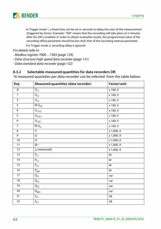
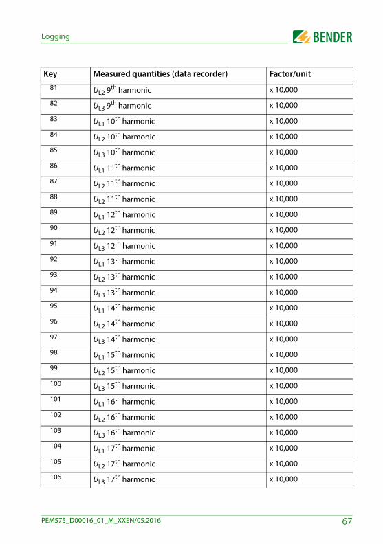
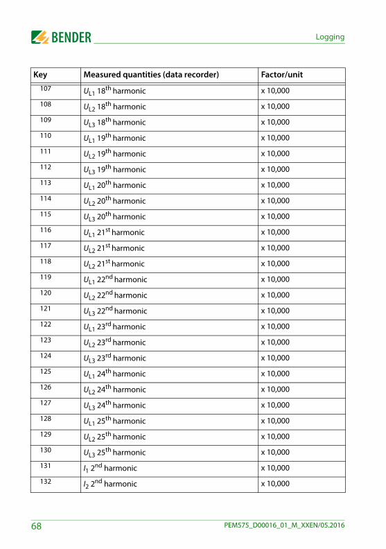
8.3.2 Selectable measured quantities for data recorders DR16 measured quantities per data recorder can be selected from the table below:
Key Measured quantities (data recorder) Factor/unit
0 UL1 x 100, V
1 UL2 x 100, V
2 UL3 x 100, V
3 Ø ULN x 100, V
4 UL1L2 x 100, V
5 UL2L3 x 100, V
6 UL3L1 x 100, V
7 Ø ULL x 100, V
8 I1 x 1,000, A
9 I2 x 1,000, A
10 I3 x 1,000, A
11 Ø I x 1,000, A
12 I4 (measured) x 1,000, A
13 PL1 W
14 PL2 W
15 PL3 W
16 Pges W
17 QL1 var
18 QL2 var
19 QL3 var
20 Qges var
21 SL1 VA
22 SL2 VA
64 PEM575_D00016_01_M_XXEN/05.2016
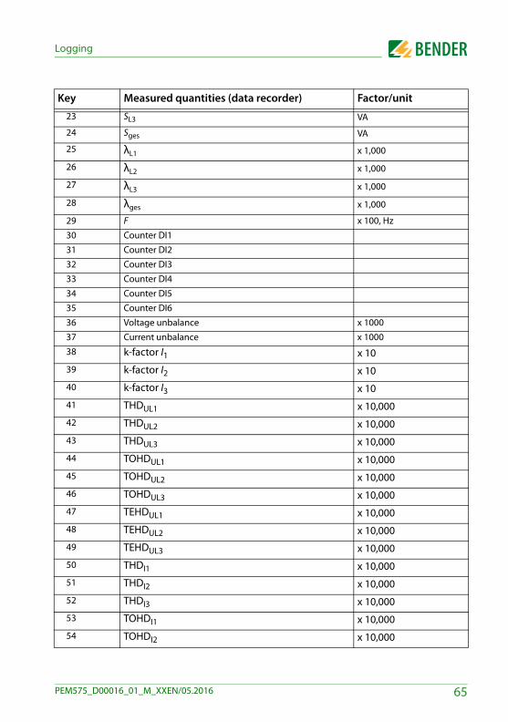
Logging
23 SL3 VA
24 Sges VA
25 λL1 x 1,000
26 λL2 x 1,000
27 λL3 x 1,000
28 λges x 1,000
29 F x 100, Hz
30 Counter DI1
31 Counter DI2
32 Counter DI3
33 Counter DI4
34 Counter DI5
35 Counter DI6
36 Voltage unbalance x 1000
37 Current unbalance x 1000
38 k-factor I1 x 1039 k-factor I2 x 1040 k-factor I3 x 1041 THDUL1 x 10,00042 THDUL2 x 10,00043 THDUL3 x 10,00044 TOHDUL1 x 10,00045 TOHDUL2 x 10,00046 TOHDUL3 x 10,00047 TEHDUL1 x 10,00048 TEHDUL2 x 10,00049 TEHDUL3 x 10,00050 THDI1 x 10,00051 THDI2 x 10,00052 THDI3 x 10,00053 TOHDI1 x 10,00054 TOHDI2 x 10,000
Key Measured quantities (data recorder) Factor/unit
65PEM575_D00016_01_M_XXEN/05.2016
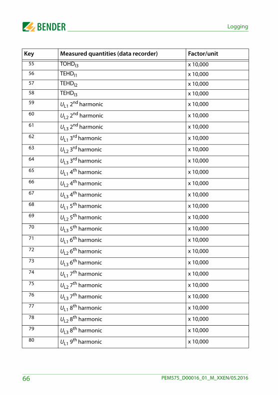
Logging
55 TOHDI3 x 10,00056 TEHDI1 x 10,00057 TEHDI2 x 10,00058 TEHDI3 x 10,00059 UL1 2nd harmonic x 10,000
60 UL2 2nd harmonic x 10,000
61 UL3 2nd harmonic x 10,000
62 UL1 3rd harmonic x 10,000
63 UL2 3rd harmonic x 10,000
64 UL3 3rd harmonic x 10,000
65 UL1 4th harmonic x 10,000
66 UL2 4th harmonic x 10,000
67 UL3 4th harmonic x 10,000
68 UL1 5th harmonic x 10,000
69 UL2 5th harmonic x 10,000
70 UL3 5th harmonic x 10,000
71 UL1 6th harmonic x 10,000
72 UL2 6th harmonic x 10,000
73 UL3 6th harmonic x 10,000
74 UL1 7th harmonic x 10,000
75 UL2 7th harmonic x 10,000
76 UL3 7th harmonic x 10,000
77 UL1 8th harmonic x 10,000
78 UL2 8th harmonic x 10,000
79 UL3 8th harmonic x 10,000
80 UL1 9th harmonic x 10,000
Key Measured quantities (data recorder) Factor/unit
66 PEM575_D00016_01_M_XXEN/05.2016
Logging
81 UL2 9th harmonic x 10,000
82 UL3 9th harmonic x 10,000
83 UL1 10th harmonic x 10,000
84 UL2 10th harmonic x 10,000
85 UL3 10th harmonic x 10,000
86 UL1 11th harmonic x 10,000
87 UL2 11th harmonic x 10,000
88 UL2 11th harmonic x 10,000
89 UL1 12th harmonic x 10,000
90 UL2 12th harmonic x 10,000
91 UL3 12th harmonic x 10,000
92 UL1 13th harmonic x 10,000
93 UL2 13th harmonic x 10,000
94 UL3 13th harmonic x 10,000
95 UL1 14th harmonic x 10,000
96 UL2 14th harmonic x 10,000
97 UL3 14th harmonic x 10,000
98 UL1 15th harmonic x 10,000
99 UL2 15th harmonic x 10,000
100 UL3 15th harmonic x 10,000
101 UL1 16th harmonic x 10,000
102 UL2 16th harmonic x 10,000
103 UL3 16th harmonic x 10,000
104 UL1 17th harmonic x 10,000
105 UL2 17th harmonic x 10,000
106 UL3 17th harmonic x 10,000
Key Measured quantities (data recorder) Factor/unit
67PEM575_D00016_01_M_XXEN/05.2016
Logging
107 UL1 18th harmonic x 10,000
108 UL2 18th harmonic x 10,000
109 UL3 18th harmonic x 10,000
110 UL1 19th harmonic x 10,000
111 UL2 19th harmonic x 10,000
112 UL3 19th harmonic x 10,000
113 UL1 20th harmonic x 10,000
114 UL2 20th harmonic x 10,000
115 UL3 20th harmonic x 10,000
116 UL1 21st harmonic x 10,000
117 UL2 21st harmonic x 10,000
118 UL2 21st harmonic x 10,000
119 UL1 22nd harmonic x 10,000
120 UL2 22nd harmonic x 10,000
121 UL3 22nd harmonic x 10,000
122 UL1 23rd harmonic x 10,000
123 UL2 23rd harmonic x 10,000
124 UL3 23rd harmonic x 10,000
125 UL1 24th harmonic x 10,000
126 UL2 24th harmonic x 10,000
127 UL3 24th harmonic x 10,000
128 UL1 25th harmonic x 10,000
129 UL2 25th harmonic x 10,000
130 UL3 25th harmonic x 10,000
131 I1 2nd harmonic x 10,000
132 I2 2nd harmonic x 10,000
Key Measured quantities (data recorder) Factor/unit
68 PEM575_D00016_01_M_XXEN/05.2016
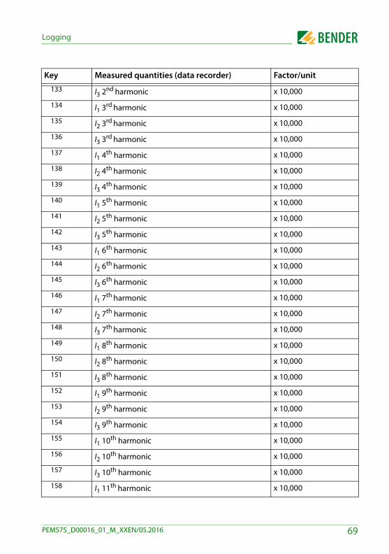
Logging
133 I3 2nd harmonic x 10,000
134 I1 3rd harmonic x 10,000
135 I2 3rd harmonic x 10,000
136 I3 3rd harmonic x 10,000
137 I1 4th harmonic x 10,000
138 I2 4th harmonic x 10,000
139 I3 4th harmonic x 10,000
140 I1 5th harmonic x 10,000
141 I2 5th harmonic x 10,000
142 I3 5th harmonic x 10,000
143 I1 6th harmonic x 10,000
144 I2 6th harmonic x 10,000
145 I3 6th harmonic x 10,000
146 I1 7th harmonic x 10,000
147 I2 7th harmonic x 10,000
148 I3 7th harmonic x 10,000
149 I1 8th harmonic x 10,000
150 I2 8th harmonic x 10,000
151 I3 8th harmonic x 10,000
152 I1 9th harmonic x 10,000
153 I2 9th harmonic x 10,000
154 I3 9th harmonic x 10,000
155 I1 10th harmonic x 10,000
156 I2 10th harmonic x 10,000
157 I3 10th harmonic x 10,000
158 I1 11th harmonic x 10,000
Key Measured quantities (data recorder) Factor/unit
69PEM575_D00016_01_M_XXEN/05.2016
Logging
159 I2 11th harmonic x 10,000
160 I2 11th harmonic x 10,000
161 I1 12th harmonic x 10,000
162 I2 12th harmonic x 10,000
163 I3 12th harmonic x 10,000
164 I1 13th harmonic x 10,000
165 I2 13th harmonic x 10,000
166 I3 13th harmonic x 10,000
167 I1 14th harmonic x 10,000
168 I2 14th harmonic x 10,000
169 I3 14th harmonic x 10,000
170 I1 15th harmonic x 10,000
171 I2 15th harmonic x 10,000
172 I3 15th harmonic x 10,000
173 I1 16th harmonic x 10,000
174 I2 16th harmonic x 10,000
175 I3 16th harmonic x 10,000
176 I1 17th harmonic x 10,000
177 I2 17th harmonic x 10,000
178 I3 17th harmonic x 10,000
179 I1 18th harmonic x 10,000
180 I2 18th harmonic x 10,000
181 I3 18th harmonic x 10,000
182 I1 19th harmonic x 10,000
183 I2 19th harmonic x 10,000
184 I3 19th harmonic x 10,000
Key Measured quantities (data recorder) Factor/unit
70 PEM575_D00016_01_M_XXEN/05.2016
Logging
185 I1 20th harmonic x 10,000
186 I2 20th harmonic x 10,000
187 I3 20th harmonic x 10,000
188 I1 21st harmonic x 10,000
189 I2 21st harmonic x 10,000
190 I2 21st harmonic x 10,000
191 I1 22nd harmonic x 10,000
192 I2 22nd harmonic x 10,000
193 I3 22nd harmonic x 10,000
194 I1 23rd harmonic x 10,000
195 I2 23rd harmonic x 10,000
196 I3 23rd harmonic x 10,000
197 I1 24th harmonic x 10,000
198 I2 24th harmonic x 10,000
199 I3 24th harmonic x 10,000
200 I1 25th harmonic x 10,000
201 I2 25th harmonic x 10,000
202 I3 25th harmonic x 10,000
203 Demand UL1 x 100, V204 Demand UL2 x 100, V205 Demand UL3 x 100, V206 Ø Demand ULN x 100, V207 Demand UL1L2 x 100, V208 Demand UL2L3 x 100, V209 Demand UL3L1 x 100, V210 Ø Demand ULL x 100, V211 Demand I1 x 1000, A
Key Measured quantities (data recorder) Factor/unit
71PEM575_D00016_01_M_XXEN/05.2016
Logging
212 Demand I2 x 1000, A213 Demand I3 x 1000, A214 Ø Demand I x 1000, A215 Demand I4
1) x 1000, A
216 Demand PL1 W217 Demand PL2 W218 Demand PL3 W219 Demand Pges W220 Demand QL1 var221 Demand QL2 var222 Demand QL3 var223 Demand Qges var224 Demand SL1 VA225 Demand SL2 VA226 Demand SL3 VA227 Demand Sges VA228 Demand λ1 x 1000229 Demand λ2 x 1000230 Demand λ3 x 1000231 Demand λges x 1000232 Demand f x 100, Hz233 Demand voltage unbalance x 1000234 Demand current unbalance x 1000235 Demand THDUL1 x 10,000236 Demand THDUL2 x 10,000237 Demand THDUL3 x 10,000238 Demand THDI1 x 10,000239 Demand THDI2 x 10,000240 Demand THDI3 x 10,000241 UL1 max (per demand period) x 100, V
Key Measured quantities (data recorder) Factor/unit
72 PEM575_D00016_01_M_XXEN/05.2016
Logging
242 UL2 max (per demand period) x 100, V243 UL3 max (per demand period) x 100, V244 Ø ULN max (per demand period) x 100, V245 UL1L2 max (per demand period) x 100, V246 UL2L3 max (per demand period) x 100, V247 UL3L1 max (per demand period) x 100, V248 Ø ULL max (per demand period) x 100, V249 I1 max (per demand period) x 1000, A250 I2 max (per demand period) x 1000, A251 I3 max (per demand period) x 1000, A252 Ø I max (per demand period) x 1000, A253 I4 max (per demand period) x 1000, A254 PL1 max (per demand period) W255 PL2 max (per demand period) W256 PL3 max (per demand period) W257 Pges max (per demand period) W258 QL1 max (per demand period) var259 QL2 max (per demand period) var260 QL3 max (per demand period) var261 Qges max (per demand period) var262 SL1 max (per demand period) VA263 SL2 max (per demand period) VA264 SL3 max (per demand period) VA265 Sges max (per demand period) VA266 λ1 max (per demand period) x 1000267 λ2 max (per demand period) x 1000268 λ3 max (per demand period) x 1000269 λges max (per demand period) x 1000270 f max (per demand period) x 100, Hz
Key Measured quantities (data recorder) Factor/unit
73PEM575_D00016_01_M_XXEN/05.2016
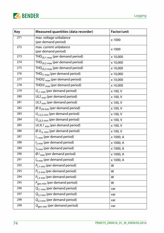
Logging
271 max. voltage unbalance(per demand period)
x 1000
272 max. current unbalance(per demand period)
x 1000
273 THDUL1 max (per demand period) x 10,000274 THDUL2 max (per demand period) x 10,000275 THDUL3 max (per demand period) x 10,000276 THDI1 max (per demand period) x 10,000277 THDI2 max (per demand period) x 10,000278 THDI3 max (per demand period) x 10,000279 UL1 min (per demand period) x 100, V280 UL2 min (per demand period) x 100, V281 UL3 min (per demand period) x 100, V282 Ø ULN min (per demand period) x 100, V283 UL1L2 min (per demand period) x 100, V284 UL2L3 min (per demand period) x 100, V285 UL3L1 min (per demand period) x 100, V286 Ø ULL min (per demand period) x 100, V287 I1 min (per demand period) x 1000, A288 I2 min (per demand period) x 1000, A289 I3 min (per demand period) x 1000, A290 Ø I min (per demand period) x 1000, A291 I4 min (per demand period) x 1000, A292 PL1 min (per demand period) W293 PL2 min (per demand period) W294 PL3 min (per demand period) W295 Pges min (per demand period) W296 QL1 min (per demand period) var297 QL2 min (per demand period) var298 QL3 min (per demand period) var299 Qges min (per demand period) var
Key Measured quantities (data recorder) Factor/unit
74 PEM575_D00016_01_M_XXEN/05.2016
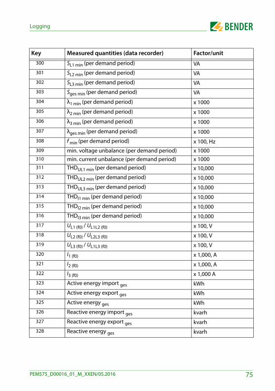
Logging
300 SL1 min (per demand period) VA301 SL2 min (per demand period) VA302 SL3 min (per demand period) VA303 Sges min (per demand period) VA304 λ1 min (per demand period) x 1000305 λ2 min (per demand period) x 1000306 λ3 min (per demand period) x 1000307 λges min (per demand period) x 1000308 f min (per demand period) x 100, Hz309 min. voltage unbalance (per demand period) x 1000310 min. current unbalance (per demand period) x 1000311 THDUL1 min (per demand period) x 10,000312 THDUL2 min (per demand period) x 10,000313 THDUL3 min (per demand period) x 10,000314 THDI1 min (per demand period) x 10,000315 THDI2 min (per demand period) x 10,000316 THDI3 min (per demand period) x 10,000317 UL1 (f0) / UL1L2 (f0) x 100, V318 UL2 (f0) / UL2L3 (f0) x 100, V319 UL3 (f0) / UL1L3 (f0) x 100, V320 I1 (f0) x 1,000, A321 I2 (f0) x 1,000, A322 I3 (f0) x 1,000 A323 Active energy import ges kWh324 Active energy export ges kWh325 Active energy ges kWh326 Reactive energy import ges kvarh327 Reactive energy export ges kvarh328 Reactive energy ges kvarh
Key Measured quantities (data recorder) Factor/unit
75PEM575_D00016_01_M_XXEN/05.2016
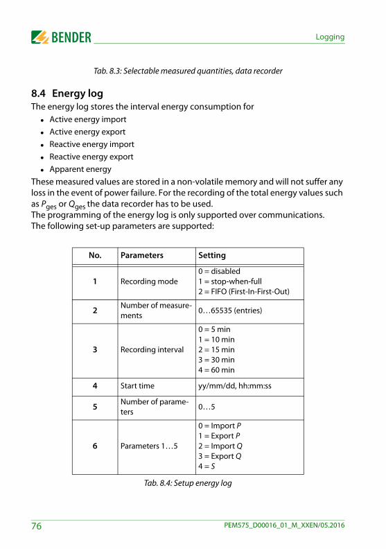
Logging
Tab. 8.3: Selectable measured quantities, data recorder
8.4 Energy logThe energy log stores the interval energy consumption for Active energy import Active energy export Reactive energy import Reactive energy export Apparent energyThese measured values are stored in a non-volatile memory and will not suffer any loss in the event of power failure. For the recording of the total energy values such as Pges or Qges the data recorder has to be used.The programming of the energy log is only supported over communications. The following set-up parameters are supported:
Tab. 8.4: Setup energy log
No. Parameters Setting
1 Recording mode0 = disabled1 = stop-when-full2 = FIFO (First-In-First-Out)
2 Number of measure-ments
0…65535 (entries)
3 Recording interval
0 = 5 min1 = 10 min2 = 15 min3 = 30 min4 = 60 min
4 Start time yy/mm/dd, hh:mm:ss
5 Number of parame-ters
0…5
6 Parameters 1…5
0 = Import P1 = Export P2 = Import Q3 = Export Q4 = S
76 PEM575_D00016_01_M_XXEN/05.2016

Logging
The energy log will only become active when the values of the Setup settings 1…5 are all non-zero.For details refer to Modbus registers 7700…7712.
8.5 Waveform recording (WFR)The PEM575 provides two waveform recorders capable of recording waveforms independently from one another. The total capacity of WFR 1 and WFR 2 is 32. Each waveform recorder can simultaneously record 3-phase voltage and current signals at a maximum resolution of 256 samples per cycle. Waveform recorders can be triggered by Setpoints Undervoltage/overvoltage (sag/swell) Transient events Communications interface (manual)
During this process the control via communications interface has the highest priority. Other WFR triggers will be ignored until recording is completed.
Each WFR log has a capacity of 32 entries. If there are more than 32 entries, the newest entry will replace the oldest entry on a first-in-first-out basis: Der 33rd entry overwrites the 1st entry, the 34th the 2nd etc.WFR data is stored in a non-volatile memory and will not suffer any loss in the event of power failure.
The programming of the waveform recorder log is only supported by the communications interface. For details about the applied registers and their data structure refer to page 133. The following set-up parameters are supported:
No. Parameters Setting
1 Number of measurements 0…32 (entries)
2 Number of samples per cycle 16, 32, 64, 128, 256 samples
3 Cycles per record 320, 160, 80, 40, 20 cycles
4 Number of cycles before the event 0…10 cycles
77PEM575_D00016_01_M_XXEN/05.2016
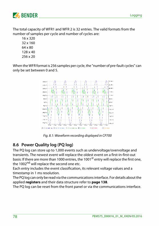
Logging
The total capacity of WFR1 and WFR 2 is 32 entries. The valid formats from the number of samples per cycle and number of cycles are:
16 x 32032 x 16064 x 80128 x 40256 x 20
When the WFR format is 256 samples per cycle, the "number of pre-fault cycles" can only be set between 0 and 5.
Fig. 8.1: Waveform recording displayed in CP700
8.6 Power Quality log (PQ log)The PQ log can store up to 1,000 events such as undervoltage/overvoltage and transients. The newest event will replace the oldest event on a first-in-first-out basis: If there are more than 1000 entries, the 1001st entry will replace the first one, the 1002nd will replace the second one etc.Each entry includes the event classification, its relevant voltage values and a timestamp in 1 ms resolution. The PQ log can only be read via the communications interface. For details about the applied registers and their data structure refer to page 138.The PQ log can be reset from the front panel or via the communications interface.
78 PEM575_D00016_01_M_XXEN/05.2016
Logging
8.7 Event log (SOE log)The device can store up to 512 events. The newest event will replace the oldest event on a first-in-first-out basis: The 513th event overwrites the first event, the 514th the second one, etc. Possible events: Failure supply voltage Setpoint status change Relay actions Digital input status changes Setup changes Each event record includes the event classification, the relevant parameter values and a timestamp in 1 ms resolution. All event entries can be retrieved via the communications interface. For details about the applied registers and their data structure refer to page 139.The event log can be cleared using the buttons on the front panel or via communications interface.
79PEM575_D00016_01_M_XXEN/05.2016

Logging
80 PEM575_D00016_01_M_XXEN/05.2016
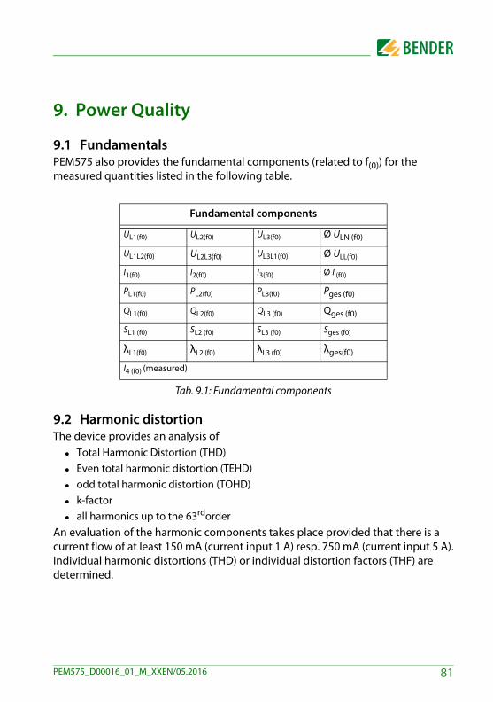
9. Power Quality
9.1 FundamentalsPEM575 also provides the fundamental components (related to f(0)) for the measured quantities listed in the following table.
Tab. 9.1: Fundamental components
9.2 Harmonic distortionThe device provides an analysis of Total Harmonic Distortion (THD) Even total harmonic distortion (TEHD) odd total harmonic distortion (TOHD) k-factor all harmonics up to the 63rdorderAn evaluation of the harmonic components takes place provided that there is a current flow of at least 150 mA (current input 1 A) resp. 750 mA (current input 5 A).Individual harmonic distortions (THD) or individual distortion factors (THF) are determined.
Fundamental components
UL1(f0) UL2(f0) UL3(f0) Ø ULN (f0)
UL1L2(f0) UL2L3(f0) UL3L1(f0) Ø ULL(f0)
I1(f0) I2(f0) I3(f0) Ø I (f0)
PL1(f0) PL2(f0) PL3(f0) Pges (f0)
QL1(f0) QL2(f0) QL3 (f0) Qges (f0)
SL1 (f0) SL2 (f0) SL3 (f0) Sges (f0)
λL1(f0) λL2 (f0) λL3 (f0) λges(f0)
I4 (f0) (measured)
81PEM575_D00016_01_M_XXEN/05.2016
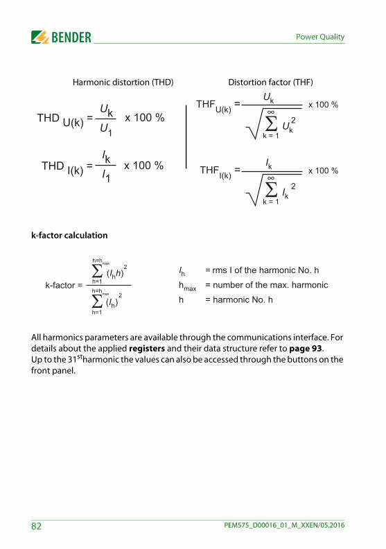
Power Quality
k-factor calculation
All harmonics parameters are available through the communications interface. For details about the applied registers and their data structure refer to page 93.Up to the 31stharmonic the values can also be accessed through the buttons on the front panel.
THD U(k) = UkU1
x 100 %
THD I(k) = IkI1
x 100 %
Uk
Uk Σ∞
k = 1
THFU(k) = 2
x 100 %
Ik
Ik Σ∞
k = 1
THFI(k) = 2
x 100 %
Harmonic distortion (THD) Distortion factor (THF)
Σ
(Ihh)Σ 2 Ih = rms I of the harmonic No. h
hmax = number of the max. harmonic
h = harmonic No. h2
h=1
h=hmax
h=hmax
h=1k-factor =
(Ih)
82 PEM575_D00016_01_M_XXEN/05.2016
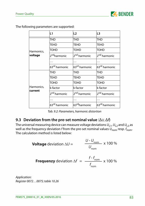
Power Quality
The following parameters are supported:
Tab. 9.2: Parameters, harmonic distortion
9.3 Deviation from the pre-set nominal value (ΔU, Δf)The universal measuring device can measure voltage deviations UL1, UL2 and UL3 as well as the frequency deviation f from the pre-set nominal values Unom resp. fnom. The calculation method is listed below:
Application: Register 0072…0075; table 10.26
L1 L2 L3
Harmonics,voltage
THD THD THD
TEHD TEHD TEHD
TOHD TOHD TOHD
2ndharmonic 2nd harmonic 2nd harmonic
… … …
63rd harmonic 63rd harmonic 63rd harmonic
Harmonics,current
THD THD THD
TEHD TEHD TEHD
TOHD TOHD TOHD
k-factor k-factor k-factor
2nd harmonic 2nd harmonic 2nd harmonic
… … …
63rd harmonic 63rdharmonic 63rd harmonic
Voltage deviation ΔU = Unom
U - Unom x 100 %
Frequenzy deviation Δf = x 100 %fnom
f - fnom
83PEM575_D00016_01_M_XXEN/05.2016
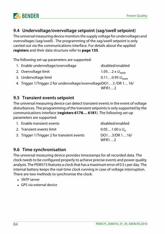
Power Quality
9.4 Undervoltage/overvoltage setpoint (sag/swell setpoint)The universal measuring device monitors the supply voltage for undervoltages and overvoltages (sag/swell) . The programming of the sag/swell setpoint is only carried out via the communications interface. For details about the applied registers and their data structure refer to page 135.
The following set-up parameters are supported:
1. Enable undervoltage/overvoltage disabled/enabled
2. Overvoltage limit 1.05…2 x Unom
3. Undervoltage limit 0.11…0.95 Unom
4. Trigger 1/Trigger 2 for undervoltage/overvoltageDO1…3 /DR 1…16/WFR1…2
9.5 Transient events setpointThe universal measuring device can detect transient events in the event of voltage disturbances. The programming of the transient setpoints is only supported by the communications interface (registers 6178… 6181). The following set-up parameters are supported:
1. Enable transient events disabled/enabled
2. Transient events limit 0.05…1.00 x Un
3. Trigger 1/Trigger 2 for transient events DO1…3/DR 1…16/ WFR1…2
9.6 Time synchronisationThe universal measuring device provides timestamps for all recorded data. The clock needs to be configured properly to achieve precise events and power quality analysis. The PEM575 features a clock that has a maximum error of 0.5 s per day. The internal battery keeps the real-time clock running in case of voltage interruption. There are two methods to synchronise the clock: SNTP server GPS via external device
84 PEM575_D00016_01_M_XXEN/05.2016
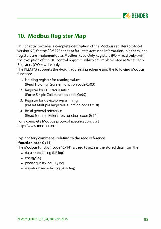
10. Modbus Register Map
This chapter provides a complete description of the Modbus register (protocol version 6.0) for the PEM575 series to facilitate access to information. In general, the registers are implemented as Modbus Read Only Registers (RO = read only). with the exception of the DO control registers, which are implemented as Write Only Registers (WO = write only).The PEM575 supports the 4-digit addressing scheme and the following Modbus functions.
1. Holding register for reading values (Read Holding Register; function code 0x03)
2. Register for DO status setup(Force Single Coil; function code 0x05)
3. Register for device programming(Preset Multiple Registers; function code 0x10)
4. Read general reference(Read General Reference; function code 0x14)
For a complete Modbus protocol specification, visit http://www.modbus.org.
Explanatory comments relating to the read reference(function code 0x14)The Modbus function code "0x14" is used to access the stored data from the data recorder log (DR log) energy log power quality log (PQ log) waveform recorder log (WFR log)
85PEM575_D00016_01_M_XXEN/05.2016
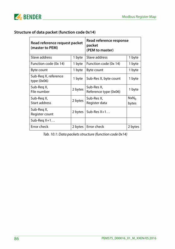
Modbus Register Map
Structure of data packet (function code 0x14)
Tab. 10.1: Data packets structure (function code 0x14)
Read reference request packet(master to PEM)
Read reference response packet(PEM to master)
Slave address 1 byte Slave address 1 byte
Function code (0x 14) 1 byte Function code (0x 14) 1 byte
Byte count 1 byte Byte count 1 byte
Sub-Req X, reference type (0x06)
1 byte Sub-Res X, byte count 1 byte
Sub-Req X,File number
2 bytesSub-Res X,Reference type (0x06)
1 byte
Sub-Req X,Start address
2 bytesSub-Res X,Register data
NxN0 bytes
Sub-Req X,Register count
2 bytes Sub-Res X+1…
Sub-Req X+1…
Error check 2 bytes Error check 2 bytes
86 PEM575_D00016_01_M_XXEN/05.2016
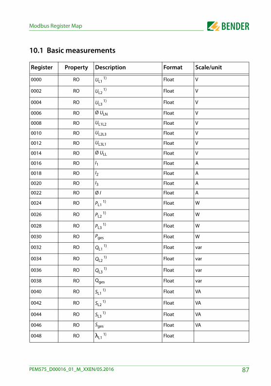
Modbus Register Map
10.1 Basic measurements
Register Property Description Format Scale/unit
0000 RO UL1 1) Float V
0002 RO UL2 1) Float V
0004 RO UL3 1) Float V
0006 RO Ø ULN Float V
0008 RO UL1L2 Float V
0010 RO UL2L3 Float V
0012 RO UL3L1 Float V
0014 RO Ø ULL Float V
0016 RO I1 Float A
0018 RO I2 Float A
0020 RO I3 Float A
0022 RO Ø I Float A
0024 RO PL1 1) Float W
0026 RO PL2 1) Float W
0028 RO PL3 1) Float W
0030 RO Pges Float W
0032 RO QL1 1) Float var
0034 RO QL2 1) Float var
0036 RO QL3 1) Float var
0038 RO Qges Float var
0040 RO SL1 1) Float VA
0042 RO SL2 1) Float VA
0044 RO SL3 1) Float VA
0046 RO Sges Float VA
0048 RO λL1 1) Float
87PEM575_D00016_01_M_XXEN/05.2016
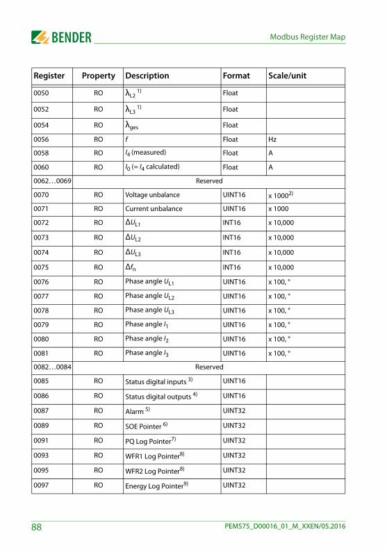
Modbus Register Map
0050 RO λL2 1) Float
0052 RO λL3 1) Float
0054 RO λges Float
0056 RO f Float Hz
0058 RO I4 (measured) Float A
0060 RO I0 (= I4 calculated) Float A
0062…0069 Reserved
0070 RO Voltage unbalance UINT16 x 10002)
0071 RO Current unbalance UINT16 x 1000
0072 RO ΔUL1 INT16 x 10,000
0073 RO ΔUL2 INT16 x 10,000
0074 RO ΔUL3 INT16 x 10,000
0075 RO Δfn INT16 x 10,000
0076 RO Phase angle UL1 UINT16 x 100, °
0077 RO Phase angle UL2 UINT16 x 100, °
0078 RO Phase angle UL3 UINT16 x 100, °
0079 RO Phase angle I1 UINT16 x 100, °
0080 RO Phase angle I2 UINT16 x 100, °
0081 RO Phase angle I3 UINT16 x 100, °
0082…0084 Reserved
0085 RO Status digital inputs 3) UINT16
0086 RO Status digital outputs 4) UINT16
0087 RO Alarm 5) UINT32
0089 RO SOE Pointer 6) UINT32
0091 RO PQ Log Pointer7) UINT32
0093 RO WFR1 Log Pointer8) UINT32
0095 RO WFR2 Log Pointer8) UINT32
0097 RO Energy Log Pointer9) UINT32
Register Property Description Format Scale/unit
88 PEM575_D00016_01_M_XXEN/05.2016
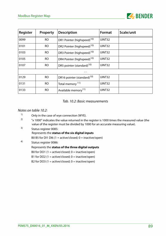
Modbus Register Map
Tab. 10.2: Basic measurements
Notes on table 10.2:1) Only in the case of wye connection (WYE).2) "x 1000" indicates the value returned in the register is 1000 times the measured value (the
value of the register must be divided by 1000 for an accurate measuring value).3) Status register 0085:
Represents the status of the six digital inputs
B0 B5 for DI1 DI6 (1 = active/closed; 0 = inactive/open)4) Status register 0086:
Represents the status of the three digital outputsB0 for DO1 (1 = active/closed; 0 = inactive/open)
B1 for DO2 (1 = active/closed; 0 = inactive/open)
B2 for DO3 (1 = active/closed; 0 = inactive/open)
0099 RO DR1 Pointer (highspeed)10) UINT32
0101 RO DR2 Pointer (highspeed)10) UINT32
0103 RO DR3 Pointer (highspeed)10) UINT32
0105 RO DR4 Pointer (highspeed)10) UINT32
0107 RO DR5 pointer (standard)10) UINT32
…
0129 RO DR16 pointer (standard)10) UINT32
0131 RO Total memory 11) UINT32
0133 RO Available memory11) UINT32
Register Property Description Format Scale/unit
89PEM575_D00016_01_M_XXEN/05.2016
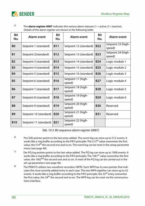
Modbus Register Map
5) The alarm register 0087 indicates the various alarm statuses (1 = active, 0 = inactive). Details of the alarm register are shown in the following table:
Tab. 10.3: Bit sequence alarm register (0087)
6) The SOE pointer points to the last entry added. The event log can store up to 512 events. It works like a ring buffer according to the FIFO principle: The 513rd value overwrites the first value, the 514th the second one and so on. The event log can be reset in the setup parameter menu (see page 46).
7) Der PQ log pointer points to the last value added. The PQ log can store up to 1000 events. It works like a ring buffer according to the FIFO principle: The 1001st value overwrites the first value, the 1002nd the second one and so on. A reset of the PQ log can be carried out in the set-up parameters (see page 46).
8) The PEM575 utilises two waveform recorders (WFR). Each WFR has its own pointer that indi-cates the most recently added entry in each case. The two WFR together can store up to 32 events. It works like a ring buffer according to the FIFO principle: the 33rd entry overwrites the first value, the 34th the second and so on. The WFR log can be reset via the communica-tions interface.
Bit No. Alarm event Bit
No. Alarm event Bit No. Alarm event
B0 Setpoint 1 (standard) B11 Setpoint 12 (standard) B22 Setpoint 23 (high-speed)
B1 Setpoint 2(standard) B12 Setpoint 13 (standard) B23 Setpoint 24 (high-speed)
B2 Setpoint 3 (standard) B13 Setpoint 14 (standard) B24 Logic module 1
B3 Setpoint 4 (standard) B14 Setpoint 15 (standard) B25 Logic module 2
B4 Setpoint 5 (standard) B15 Setpoint 16 (standard) B26 Logic module 3
B5 Setpoint 6 (standard) B16 Setpoint 17 (high-speed)
B27 Logic module 4
B6 Setpoint 7 (standard) B17 Setpoint 18 (high-speed)
B28 Logic module 5
B7 Setpoint 8 (standard) B18 Setpoint 19 (high-speed)
B29 Logic module 6
B8 Setpoint 9 (standard) B19 Setpoint 20 (high-speed)
B30 Reserved
B9 Setpoint 10 (standard) B20 Setpoint 21 (high-speed)
B31 Reserved
B10 Setpoint 11 (standard) B21 Setpoint 22 (high-speed)
90 PEM575_D00016_01_M_XXEN/05.2016
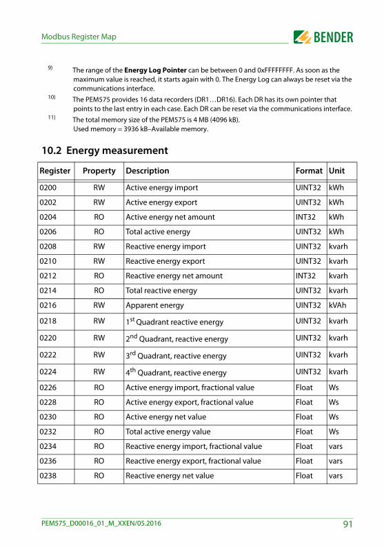
Modbus Register Map
9) The range of the Energy Log Pointer can be between 0 and 0xFFFFFFFF. As soon as the maximum value is reached, it starts again with 0. The Energy Log can always be reset via the communications interface.
10) The PEM575 provides 16 data recorders (DR1…DR16). Each DR has its own pointer that points to the last entry in each case. Each DR can be reset via the communications interface.
11) The total memory size of the PEM575 is 4 MB (4096 kB). Used memory = 3936 kB–Available memory.
10.2 Energy measurement
Register Property Description Format Unit
0200 RW Active energy import UINT32 kWh
0202 RW Active energy export UINT32 kWh
0204 RO Active energy net amount INT32 kWh
0206 RO Total active energy UINT32 kWh
0208 RW Reactive energy import UINT32 kvarh
0210 RW Reactive energy export UINT32 kvarh
0212 RO Reactive energy net amount INT32 kvarh
0214 RO Total reactive energy UINT32 kvarh
0216 RW Apparent energy UINT32 kVAh
0218 RW 1st Quadrant reactive energy UINT32 kvarh
0220 RW 2nd Quadrant, reactive energy UINT32 kvarh
0222 RW 3rd Quadrant, reactive energy UINT32 kvarh
0224 RW 4th Quadrant, reactive energy UINT32 kvarh
0226 RO Active energy import, fractional value Float Ws
0228 RO Active energy export, fractional value Float Ws
0230 RO Active energy net value Float Ws
0232 RO Total active energy value Float Ws
0234 RO Reactive energy import, fractional value Float vars
0236 RO Reactive energy export, fractional value Float vars
0238 RO Reactive energy net value Float vars
91PEM575_D00016_01_M_XXEN/05.2016
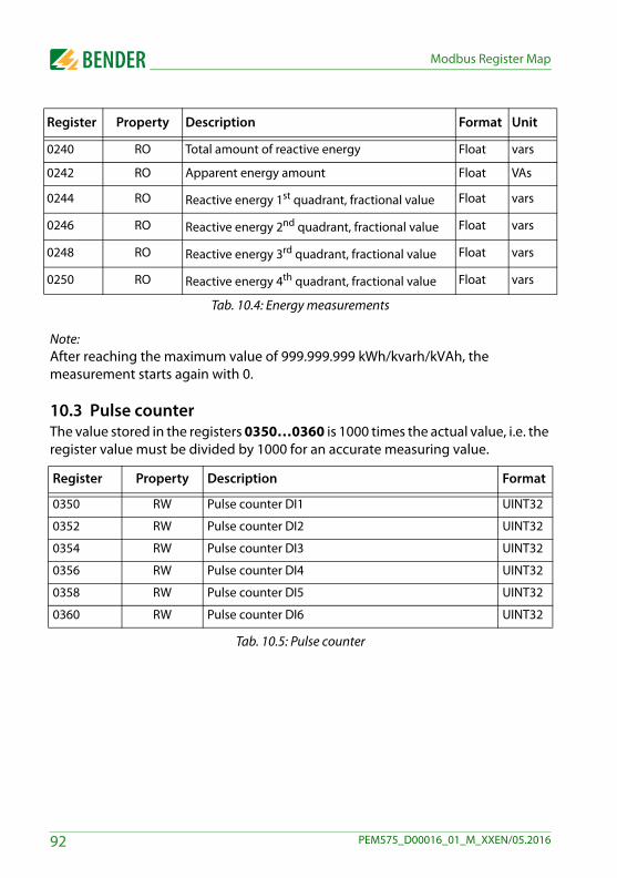
Modbus Register Map
Tab. 10.4: Energy measurements
Note: After reaching the maximum value of 999.999.999 kWh/kvarh/kVAh, the measurement starts again with 0.
10.3 Pulse counterThe value stored in the registers 0350…0360 is 1000 times the actual value, i.e. the register value must be divided by 1000 for an accurate measuring value.
Tab. 10.5: Pulse counter
0240 RO Total amount of reactive energy Float vars
0242 RO Apparent energy amount Float VAs
0244 RO Reactive energy 1st quadrant, fractional value Float vars
0246 RO Reactive energy 2nd quadrant, fractional value Float vars
0248 RO Reactive energy 3rd quadrant, fractional value Float vars
0250 RO Reactive energy 4th quadrant, fractional value Float vars
Register Property Description Format
0350 RW Pulse counter DI1 UINT32
0352 RW Pulse counter DI2 UINT32
0354 RW Pulse counter DI3 UINT32
0356 RW Pulse counter DI4 UINT32
0358 RW Pulse counter DI5 UINT32
0360 RW Pulse counter DI6 UINT32
Register Property Description Format Unit
92 PEM575_D00016_01_M_XXEN/05.2016
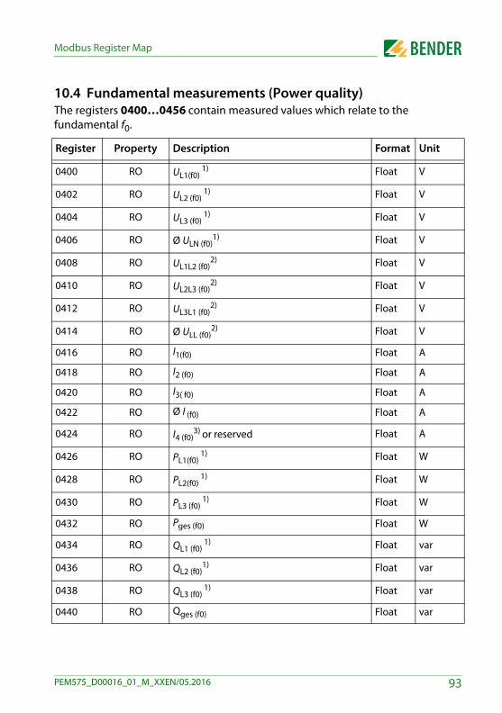
Modbus Register Map
10.4 Fundamental measurements (Power quality)The registers 0400…0456 contain measured values which relate to the fundamental f0.
Register Property Description Format Unit
0400 RO UL1(f0) 1) Float V
0402 RO UL2 (f0) 1) Float V
0404 RO UL3 (f0) 1) Float V
0406 RO Ø ULN (f0)1) Float V
0408 RO UL1L2 (f0)2) Float V
0410 RO UL2L3 (f0)2) Float V
0412 RO UL3L1 (f0)2) Float V
0414 RO Ø ULL (f0)2) Float V
0416 RO I1(f0) Float A
0418 RO I2 (f0) Float A
0420 RO I3( f0) Float A
0422 RO Ø I (f0) Float A
0424 RO I4 (f0)3) or reserved Float A
0426 RO PL1(f0) 1) Float W
0428 RO PL2(f0) 1) Float W
0430 RO PL3 (f0) 1) Float W
0432 RO Pges (f0) Float W
0434 RO QL1 (f0) 1) Float var
0436 RO QL2 (f0)1) Float var
0438 RO QL3 (f0) 1) Float var
0440 RO Qges (f0) Float var
93PEM575_D00016_01_M_XXEN/05.2016
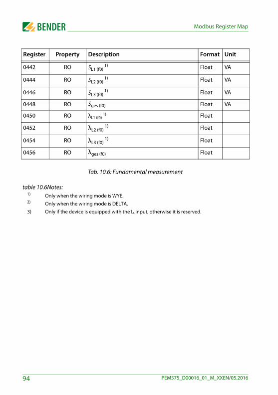
Modbus Register Map
Tab. 10.6: Fundamental measurement
table 10.6Notes:1) Only when the wiring mode is WYE.2) Only when the wiring mode is DELTA.
3) Only if the device is equipped with the I4 input, otherwise it is reserved.
0442 RO SL1 (f0) 1) Float VA
0444 RO SL2 (f0) 1) Float VA
0446 RO SL3 (f0) 1) Float VA
0448 RO Sges (f0) Float VA
0450 RO λL1 (f0) 1) Float
0452 RO λL2 (f0) 1) Float
0454 RO λL3 (f0) 1) Float
0456 RO λges (f0) Float
Register Property Description Format Unit
94 PEM575_D00016_01_M_XXEN/05.2016
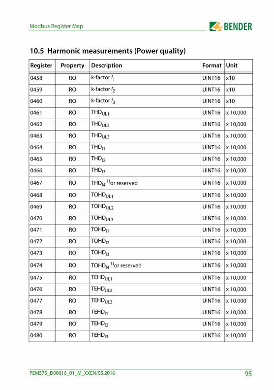
Modbus Register Map
10.5 Harmonic measurements (Power quality)
Register Property Description Format Unit
0458 RO k-factor I1 UINT16 x10
0459 RO k-factor I2 UINT16 x10
0460 RO k-factor I3 UINT16 x10
0461 RO THDUL1 UINT16 x 10,000
0462 RO THDUL2 UINT16 x 10,000
0463 RO THDUL3 UINT16 x 10,000
0464 RO THDI1 UINT16 x 10,000
0465 RO THDI2 UINT16 x 10,000
0466 RO THDI3 UINT16 x 10,000
0467 RO THDI4 1)or reserved UINT16 x 10,000
0468 RO TOHDUL1 UINT16 x 10,000
0469 RO TOHDUL2 UINT16 x 10,000
0470 RO TOHDUL3 UINT16 x 10,000
0471 RO TOHDI1 UINT16 x 10,000
0472 RO TOHDI2 UINT16 x 10,000
0473 RO TOHDI3 UINT16 x 10,000
0474 RO TOHDI4 1)or reserved UINT16 x 10,000
0475 RO TEHDUL1 UINT16 x 10,000
0476 RO TEHDUL2 UINT16 x 10,000
0477 RO TEHDUL3 UINT16 x 10,000
0478 RO TEHDI1 UINT16 x 10,000
0479 RO TEHDI2 UINT16 x 10,000
0480 RO TEHDI3 UINT16 x 10,000
95PEM575_D00016_01_M_XXEN/05.2016
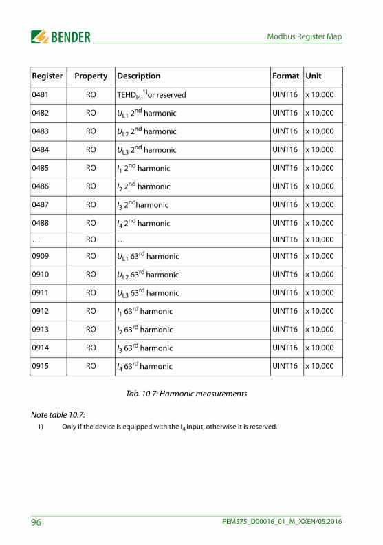
Modbus Register Map
Tab. 10.7: Harmonic measurements
Note table 10.7:1) Only if the device is equipped with the I4 input, otherwise it is reserved.
0481 RO TEHDI4 1)or reserved UINT16 x 10,000
0482 RO UL1 2nd harmonic UINT16 x 10,000
0483 RO UL2 2nd harmonic UINT16 x 10,000
0484 RO UL3 2nd harmonic UINT16 x 10,000
0485 RO I1 2nd harmonic UINT16 x 10,000
0486 RO I2 2nd harmonic UINT16 x 10,000
0487 RO I3 2ndharmonic UINT16 x 10,000
0488 RO I4 2nd harmonic UINT16 x 10,000
… RO … UINT16 x 10,000
0909 RO UL1 63rd harmonic UINT16 x 10,000
0910 RO UL2 63rd harmonic UINT16 x 10,000
0911 RO UL3 63rd harmonic UINT16 x 10,000
0912 RO I1 63rd harmonic UINT16 x 10,000
0913 RO I2 63rd harmonic UINT16 x 10,000
0914 RO I3 63rd harmonic UINT16 x 10,000
0915 RO I4 63rd harmonic UINT16 x 10,000
Register Property Description Format Unit
96 PEM575_D00016_01_M_XXEN/05.2016
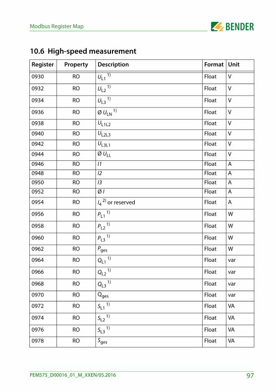
Modbus Register Map
10.6 High-speed measurement
Register Property Description Format Unit
0930 RO UL1 1) Float V
0932 RO UL2 1) Float V
0934 RO UL3 1) Float V
0936 RO Ø ULN 1) Float V
0938 RO UL1L2 Float V
0940 RO UL2L3 Float V
0942 RO UL3L1 Float V
0944 RO Ø ULL Float V
0946 RO I1 Float A
0948 RO I2 Float A
0950 RO I3 Float A
0952 RO Ø I Float A
0954 RO I4 2) or reserved Float A
0956 RO PL1 1) Float W
0958 RO PL2 1) Float W
0960 RO PL3 1) Float W
0962 RO Pges Float W
0964 RO QL1 1) Float var
0966 RO QL2 1) Float var
0968 RO QL3 1) Float var
0970 RO Qges Float var
0972 RO SL1 1) Float VA
0974 RO SL2 1) Float VA
0976 RO SL3 1) Float VA
0978 RO Sges Float VA
97PEM575_D00016_01_M_XXEN/05.2016
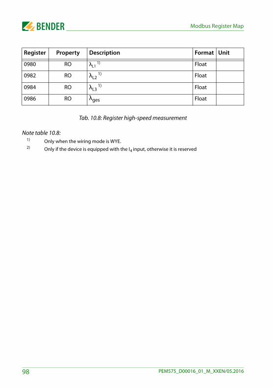
Modbus Register Map
Tab. 10.8: Register high-speed measurement
Note table 10.8:1) Only when the wiring mode is WYE.2) Only if the device is equipped with the I4 input, otherwise it is reserved
0980 RO λL1 1) Float
0982 RO λL2 1) Float
0984 RO λL3 1) Float
0986 RO λges Float
Register Property Description Format Unit
98 PEM575_D00016_01_M_XXEN/05.2016
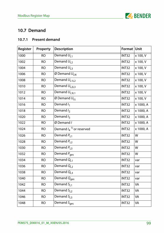
Modbus Register Map
10.7 Demand
10.7.1 Present demand
Register Property Description Format Unit
1000 RO Demand UL1 INT32 x 100, V
1002 RO Demand UL2 INT32 x 100, V
1004 RO Demand UL3 INT32 x 100, V
1006 RO Ø Demand ULN INT32 x 100, V
1008 RO Demand UL1L2 INT32 x 100, V
1010 RO Demand UL2L3 INT32 x 100, V
1012 RO Demand UL3L1 INT32 x 100, V
1014 RO Ø Demand ULL INT32 x 100, V
1016 RO Demand I1 INT32 x 1000, A
1018 RO Demand I2 INT32 x 1000, A
1020 RO Demand I3 INT32 x 1000, A
1022 RO Ø Demand I INT32 x 1000, A
1024 RO Demand I4 1) or reserved INT32 x 1000, A
1026 RO Demand PL1 INT32 W
1028 RO Demand PL2 INT32 W
1030 RO Demand PL3 INT32 W
1032 RO Demand Pges INT32 W
1034 RO Demand QL1 INT32 var
1036 RO Demand QL2 INT32 var
1038 RO Demand QL3 INT32 var
1040 RO Demand Qges INT32 var
1042 RO Demand SL1 INT32 VA
1044 RO Demand SL2 INT32 VA
1046 RO Demand SL3 INT32 VA
1048 RO Demand Sges INT32 VA
99PEM575_D00016_01_M_XXEN/05.2016
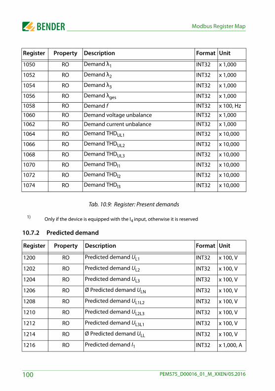
Modbus Register Map
Tab. 10.9: Register: Present demands
1) Only if the device is equipped with the I4 input, otherwise it is reserved
10.7.2 Predicted demand
1050 RO Demand λ1 INT32 x 1,000
1052 RO Demand λ2 INT32 x 1,000
1054 RO Demand λ3 INT32 x 1,000
1056 RO Demand λges INT32 x 1,000
1058 RO Demand f INT32 x 100, Hz
1060 RO Demand voltage unbalance INT32 x 1,000
1062 RO Demand current unbalance INT32 x 1,000
1064 RO Demand THDUL1 INT32 x 10,000
1066 RO Demand THDUL2 INT32 x 10,000
1068 RO Demand THDUL3 INT32 x 10,000
1070 RO Demand THDI1 INT32 x 10,000
1072 RO Demand THDI2 INT32 x 10,000
1074 RO Demand THDI3 INT32 x 10,000
Register Property Description Format Unit
1200 RO Predicted demand UL1 INT32 x 100, V
1202 RO Predicted demand UL2 INT32 x 100, V
1204 RO Predicted demand UL3 INT32 x 100, V
1206 RO Ø Predicted demand ULN INT32 x 100, V
1208 RO Predicted demand UL1L2 INT32 x 100, V
1210 RO Predicted demand UL2L3 INT32 x 100, V
1212 RO Predicted demand UL3L1 INT32 x 100, V
1214 RO Ø Predicted demand ULL INT32 x 100, V
1216 RO Predicted demand I1 INT32 x 1,000, A
Register Property Description Format Unit
100 PEM575_D00016_01_M_XXEN/05.2016

Modbus Register Map
1218 RO Predicted demand I2 INT32 x 1,000, A
1220 RO Predicted demand I3 INT32 x 1,000, A
1222 RO Ø Predicted demand I INT32 x 1,000, A
1224 RO Predicted demand I4 1) INT32 x 1,000, A
1226 RO Predicted demand PL1 INT32 W
1228 RO Predicted demand PL2 INT32 W
1230 RO Predicted demand PL3 INT32 W
1232 RO Predicted demand Pges INT32 W
1234 RO Predicted demand QL1 INT32 var
1236 RO Predicted demand QL2 INT32 var
1238 RO Predicted demand QL3 INT32 var
1240 RO Predicted demand Qges INT32 var
1242 RO Predicted demand SL1 INT32 VA
1244 RO Predicted demand SL2 INT32 VA
1246 RO Predicted demand SL3 INT32 VA
1248 RO Predicted demand Sges INT32 VA
1250 RO Predicted demand λ1 INT32 x 1,000
1252 RO Predicted demand λ2 INT32 x 1,000
1254 RO Predicted demand λ3 INT32 x 1,000
1256 RO Predicted demand λges INT32 x 1,000
1258 RO Predicted demand f INT32 x 100, Hz
1260 RO Predicted demand, voltage unbalance INT32 x 1,000
1262 RO Predicted demand, current unbalance INT32 x 1,000
1264 RO Predicted demand THDUL1 INT32 x 10,000
1266 RO Predicted demand THDUL2 INT32 x 10,000
1268 RO Predicted demand THDUL3 INT32 x 10,000
Register Property Description Format Unit
101PEM575_D00016_01_M_XXEN/05.2016
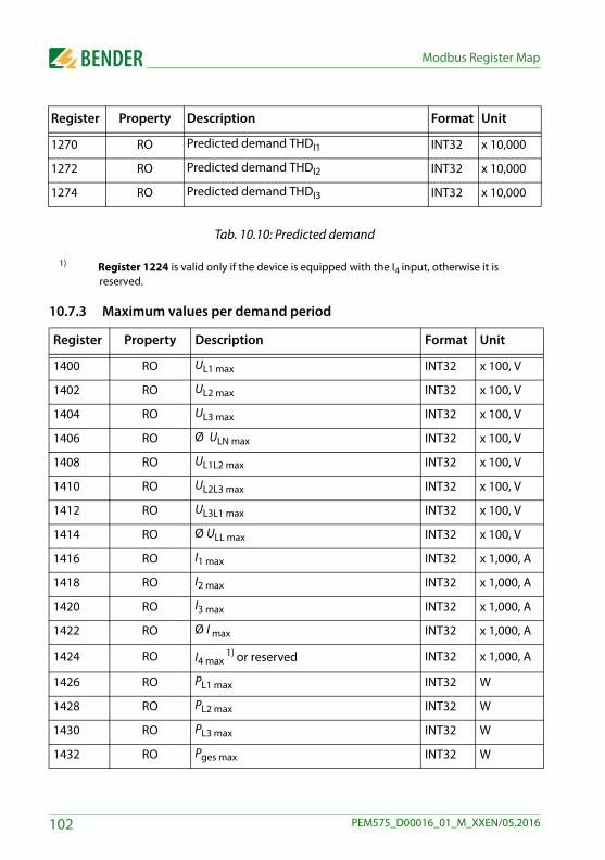
Modbus Register Map
Tab. 10.10: Predicted demand
1) Register 1224 is valid only if the device is equipped with the I4 input, otherwise it is reserved.
10.7.3 Maximum values per demand period
1270 RO Predicted demand THDI1 INT32 x 10,000
1272 RO Predicted demand THDI2 INT32 x 10,000
1274 RO Predicted demand THDI3 INT32 x 10,000
Register Property Description Format Unit
1400 RO UL1 max INT32 x 100, V
1402 RO UL2 max INT32 x 100, V
1404 RO UL3 max INT32 x 100, V
1406 RO Ø ULN max INT32 x 100, V
1408 RO UL1L2 max INT32 x 100, V
1410 RO UL2L3 max INT32 x 100, V
1412 RO UL3L1 max INT32 x 100, V
1414 RO Ø ULL max INT32 x 100, V
1416 RO I1 max INT32 x 1,000, A
1418 RO I2 max INT32 x 1,000, A
1420 RO I3 max INT32 x 1,000, A
1422 RO Ø I max INT32 x 1,000, A
1424 RO I4 max 1) or reserved INT32 x 1,000, A
1426 RO PL1 max INT32 W
1428 RO PL2 max INT32 W
1430 RO PL3 max INT32 W
1432 RO Pges max INT32 W
Register Property Description Format Unit
102 PEM575_D00016_01_M_XXEN/05.2016
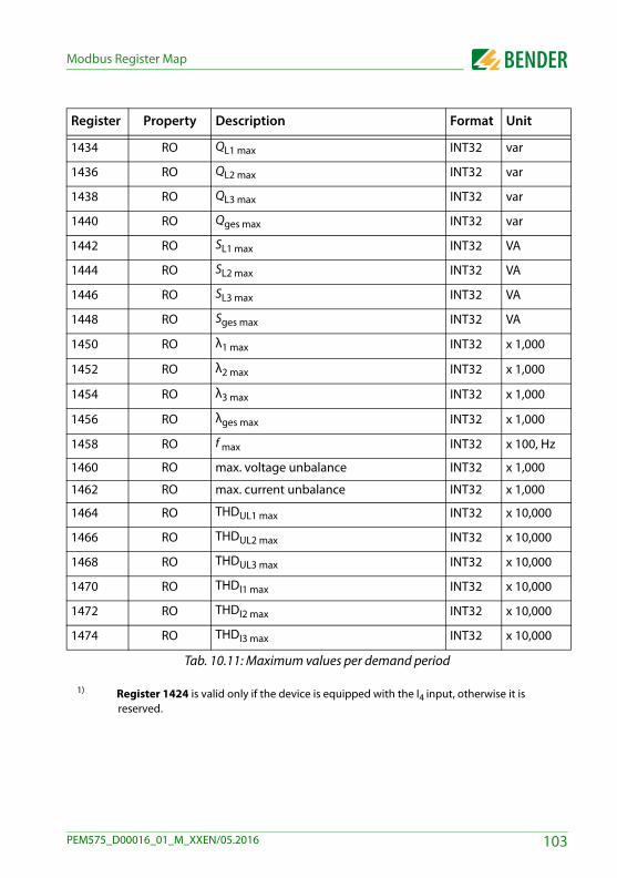
Modbus Register Map
Tab. 10.11: Maximum values per demand period
1) Register 1424 is valid only if the device is equipped with the I4 input, otherwise it is reserved.
1434 RO QL1 max INT32 var
1436 RO QL2 max INT32 var
1438 RO QL3 max INT32 var
1440 RO Qges max INT32 var
1442 RO SL1 max INT32 VA
1444 RO SL2 max INT32 VA
1446 RO SL3 max INT32 VA
1448 RO Sges max INT32 VA
1450 RO λ1 max INT32 x 1,000
1452 RO λ2 max INT32 x 1,000
1454 RO λ3 max INT32 x 1,000
1456 RO λges max INT32 x 1,000
1458 RO f max INT32 x 100, Hz
1460 RO max. voltage unbalance INT32 x 1,000
1462 RO max. current unbalance INT32 x 1,000
1464 RO THDUL1 max INT32 x 10,000
1466 RO THDUL2 max INT32 x 10,000
1468 RO THDUL3 max INT32 x 10,000
1470 RO THDI1 max INT32 x 10,000
1472 RO THDI2 max INT32 x 10,000
1474 RO THDI3 max INT32 x 10,000
Register Property Description Format Unit
103PEM575_D00016_01_M_XXEN/05.2016
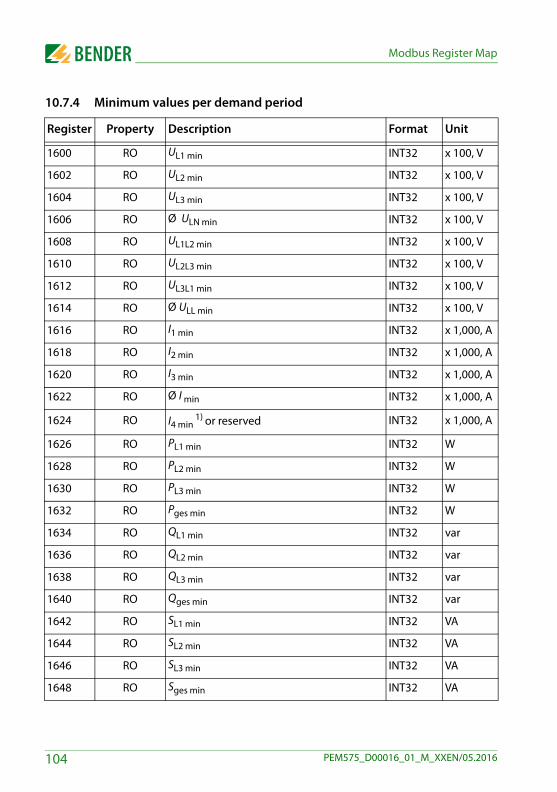
Modbus Register Map
10.7.4 Minimum values per demand period
Register Property Description Format Unit
1600 RO UL1 min INT32 x 100, V
1602 RO UL2 min INT32 x 100, V
1604 RO UL3 min INT32 x 100, V
1606 RO Ø ULN min INT32 x 100, V
1608 RO UL1L2 min INT32 x 100, V
1610 RO UL2L3 min INT32 x 100, V
1612 RO UL3L1 min INT32 x 100, V
1614 RO Ø ULL min INT32 x 100, V
1616 RO I1 min INT32 x 1,000, A
1618 RO I2 min INT32 x 1,000, A
1620 RO I3 min INT32 x 1,000, A
1622 RO Ø I min INT32 x 1,000, A
1624 RO I4 min 1) or reserved INT32 x 1,000, A
1626 RO PL1 min INT32 W
1628 RO PL2 min INT32 W
1630 RO PL3 min INT32 W
1632 RO Pges min INT32 W
1634 RO QL1 min INT32 var
1636 RO QL2 min INT32 var
1638 RO QL3 min INT32 var
1640 RO Qges min INT32 var
1642 RO SL1 min INT32 VA
1644 RO SL2 min INT32 VA
1646 RO SL3 min INT32 VA
1648 RO Sges min INT32 VA
104 PEM575_D00016_01_M_XXEN/05.2016
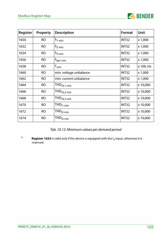
Modbus Register Map
Tab. 10.12: Minimum values per demand period
1) Register 1624 is valid only if the device is equipped with the I4 input, otherwise it is reserved.
1650 RO λ1 min INT32 x 1,000
1652 RO λ2 min INT32 x 1,000
1654 RO λ3 min INT32 x 1,000
1656 RO λges min INT32 x 1,000
1658 RO f min INT32 x 100, Hz
1660 RO min. voltage unbalance INT32 x 1,000
1662 RO min. current unbalance INT32 x 1,000
1664 RO THDUL1 min INT32 x 10,000
1666 RO THDUL2 min INT32 x 10,000
1668 RO THDUL3 min INT32 x 10,000
1670 RO THDI1 min INT32 x 10,000
1672 RO THDI2 min INT32 x 10,000
1674 RO THDI3 min INT32 x 10,000
Register Property Description Format Unit
105PEM575_D00016_01_M_XXEN/05.2016
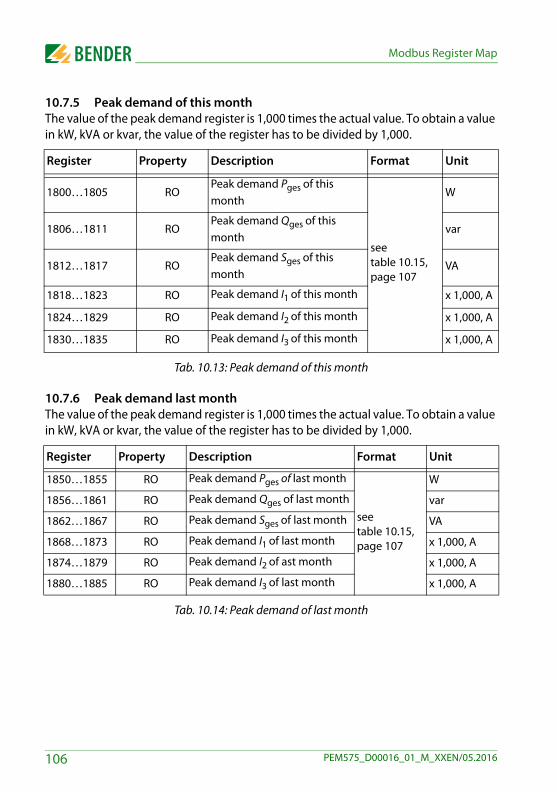
Modbus Register Map
10.7.5 Peak demand of this monthThe value of the peak demand register is 1,000 times the actual value. To obtain a value in kW, kVA or kvar, the value of the register has to be divided by 1,000.
Tab. 10.13: Peak demand of this month
10.7.6 Peak demand last monthThe value of the peak demand register is 1,000 times the actual value. To obtain a value in kW, kVA or kvar, the value of the register has to be divided by 1,000.
Tab. 10.14: Peak demand of last month
Register Property Description Format Unit
1800…1805 ROPeak demand Pges of this month
see table 10.15, page 107
W
1806…1811 ROPeak demand Qges of this month
var
1812…1817 ROPeak demand Sges of this month
VA
1818…1823 RO Peak demand I1 of this month x 1,000, A
1824…1829 RO Peak demand I2 of this month x 1,000, A
1830…1835 RO Peak demand I3 of this month x 1,000, A
Register Property Description Format Unit
1850…1855 RO Peak demand Pges of last month
see table 10.15, page 107
W
1856…1861 RO Peak demand Qges of last month var
1862…1867 RO Peak demand Sges of last month VA
1868…1873 RO Peak demand I1 of last month x 1,000, A
1874…1879 RO Peak demand I2 of ast month x 1,000, A
1880…1885 RO Peak demand I3 of last month x 1,000, A
106 PEM575_D00016_01_M_XXEN/05.2016
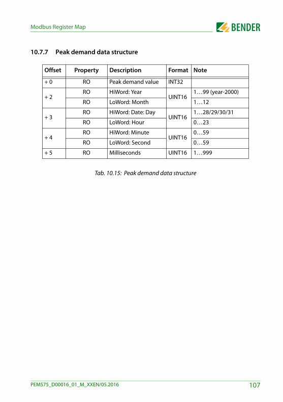
Modbus Register Map
10.7.7 Peak demand data structure
Tab. 10.15: Peak demand data structure
Offset Property Description Format Note
+ 0 RO Peak demand value INT32
+ 2RO HiWord: Year
UINT161…99 (year-2000)
RO LoWord: Month 1…12
+ 3RO HiWord: Date: Day
UINT161…28/29/30/31
RO LoWord: Hour 0…23
+ 4RO HiWord: Minute
UINT160…59
RO LoWord: Second 0…59
+ 5 RO Milliseconds UINT16 1…999
107PEM575_D00016_01_M_XXEN/05.2016
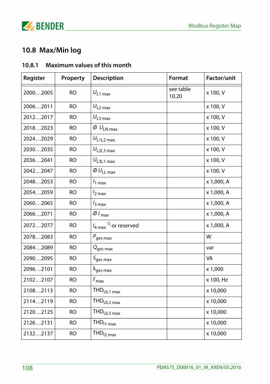
Modbus Register Map
10.8 Max/Min log
10.8.1 Maximum values of this month
Register Property Description Format Factor/unit
2000…2005 RO UL1 maxsee table 10.20
x 100, V
2006…2011 RO UL2 max x 100, V
2012…2017 RO UL3 max x 100, V
2018…2023 RO Ø ULN max x 100, V
2024…2029 RO UL1L2 max x 100, V
2030…2035 RO UL2L3 max x 100, V
2036…2041 RO UL3L1 max x 100, V
2042…2047 RO Ø ULL max x 100, V
2048…2053 RO I1 max x 1,000, A
2054…2059 RO I2 max x 1,000, A
2060…2065 RO I3 max x 1,000, A
2066…2071 RO Ø I max x 1,000, A
2072…2077 RO I4 max 1) or reserved x 1,000, A
2078…2083 RO Pges max W
2084…2089 RO Qges max var
2090…2095 RO Sges max VA
2096…2101 RO λges max x 1,000
2102…2107 RO f max x 100, Hz
2108…2113 RO THDUL1 max x 10,000
2114…2119 RO THDUL2 max x 10,000
2120…2125 RO THDUL3 max x 10,000
2126…2131 RO THDI1 max x 10,000
2132…2137 RO THDI2 max x 10,000
108 PEM575_D00016_01_M_XXEN/05.2016
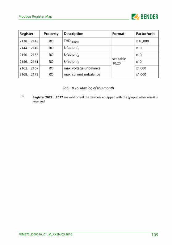
Modbus Register Map
Tab. 10.16: Max log of this month
1) Register 2072…2077 are valid only if the device is equipped with the I4 input, otherwise it is reserved
2138…2143 RO THDI3 max x 10,000
2144…2149 RO k-factor I1
see table 10.20
x10
2150…2155 RO k-factor I2 x10
2156…2161 RO k-factor I3 x10
2162…2167 RO max. voltage unbalance x1,000
2168…2173 RO max. current unbalance x1,000
Register Property Description Format Factor/unit
109PEM575_D00016_01_M_XXEN/05.2016
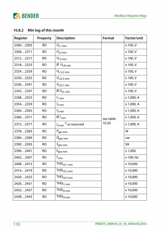
Modbus Register Map
10.8.2 Min log of this month
Register Property Description Format Factor/unit
2300…2305 RO UL1 min
see table 10.20
x 100, V
2306…2311 RO UL2 min x 100, V
2312…2317 RO UL3 min x 100, V
2318…2323 RO Ø ULN min x 100, V
2324…2329 RO UL1L2 min x 100, V
2330…2335 RO UL2L3 min x 100, V
2336…2341 RO UL3L1 min x 100, V
2342…2347 RO Ø ULL min x 100, V
2348…2353 RO I1 min x 1,000, A
2354…2359 RO I2 min x 1,000, A
2360…2365 RO I3 min x 1,000, A
2366…2371 RO Ø I min x 1,000, A
2372…2377 RO I4 min 1) or reserved x 1,000, A
2378…2383 RO Pges min W
2384…2389 RO Qges min var
2390…2395 RO Sges min VA
2396…2401 RO λges min x 1,000
2402…2407 RO f min x 100, Hz
2408…2413 RO THDUL1 min x 10,000
2414…2419 RO THDUL2 min x 10,000
2420…2425 RO THDUL3 min x 10,000
2426…2431 RO THDI1 min x 10,000
2432…2437 RO THDI2 min x 10,000
2438…2443 RO THDI3 min x 10,000
110 PEM575_D00016_01_M_XXEN/05.2016
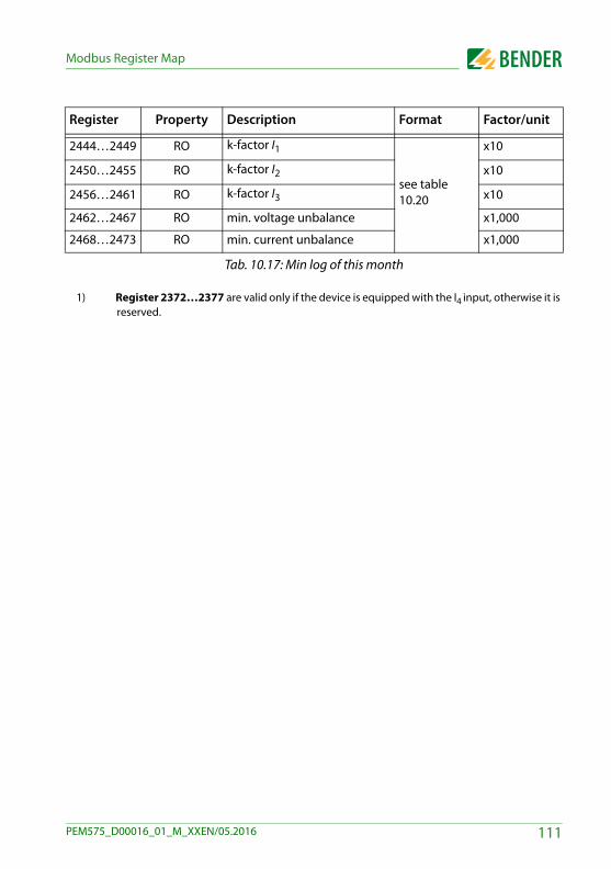
Modbus Register Map
Tab. 10.17: Min log of this month
1) Register 2372…2377 are valid only if the device is equipped with the I4 input, otherwise it is reserved.
2444…2449 RO k-factor I1
see table 10.20
x10
2450…2455 RO k-factor I2 x10
2456…2461 RO k-factor I3 x10
2462…2467 RO min. voltage unbalance x1,000
2468…2473 RO min. current unbalance x1,000
Register Property Description Format Factor/unit
111PEM575_D00016_01_M_XXEN/05.2016
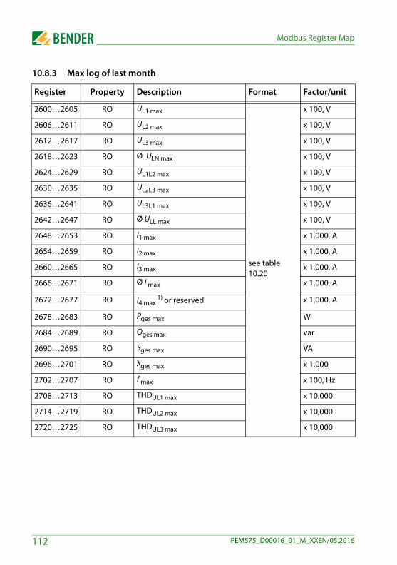
Modbus Register Map
10.8.3 Max log of last month
Register Property Description Format Factor/unit
2600…2605 RO UL1 max
see table 10.20
x 100, V
2606…2611 RO UL2 max x 100, V
2612…2617 RO UL3 max x 100, V
2618…2623 RO Ø ULN max x 100, V
2624…2629 RO UL1L2 max x 100, V
2630…2635 RO UL2L3 max x 100, V
2636…2641 RO UL3L1 max x 100, V
2642…2647 RO Ø ULL max x 100, V
2648…2653 RO I1 max x 1,000, A
2654…2659 RO I2 max x 1,000, A
2660…2665 RO I3 max x 1,000, A
2666…2671 RO Ø I max x 1,000, A
2672…2677 RO I4 max 1) or reserved x 1,000, A
2678…2683 RO Pges max W
2684…2689 RO Qges max var
2690…2695 RO Sges max VA
2696…2701 RO λges max x 1,000
2702…2707 RO f max x 100, Hz
2708…2713 RO THDUL1 max x 10,000
2714…2719 RO THDUL2 max x 10,000
2720…2725 RO THDUL3 max x 10,000
112 PEM575_D00016_01_M_XXEN/05.2016
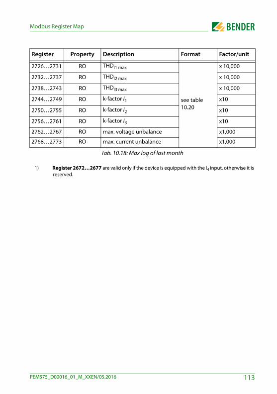
Modbus Register Map
Tab. 10.18: Max log of last month
1) Register 2672…2677 are valid only if the device is equipped with the I4 input, otherwise it is reserved.
2726…2731 RO THDI1 max
see table 10.20
x 10,000
2732…2737 RO THDI2 max x 10,000
2738…2743 RO THDI3 max x 10,000
2744…2749 RO k-factor I1 x10
2750…2755 RO k-factor I2 x10
2756…2761 RO k-factor I3 x10
2762…2767 RO max. voltage unbalance x1,000
2768…2773 RO max. current unbalance x1,000
Register Property Description Format Factor/unit
113PEM575_D00016_01_M_XXEN/05.2016
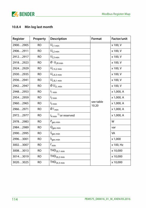
Modbus Register Map
10.8.4 Min log last month
Register Property Description Format Factor/unit
2900…2905 RO UL1 min
see table 10.20
x 100, V
2906…2911 RO UL2 min x 100, V
2912…2917 RO UL3 min x 100, V
2918…2923 RO Ø ULN min x 100, V
2924…2929 RO UL1L2 min x 100, V
2930…2935 RO UL2L3 min x 100, V
2936…2941 RO UL3L1 min x 100, V
2942…2947 RO Ø ULL min x 100, V
2948…2953 RO I1 min x 1,000, A
2954…2959 RO I2 min x 1,000, A
2960…2965 RO I3 min x 1,000, A
2966…2971 RO Ø I min x 1,000, A
2972…2977 RO I4 min 1) or reserved x 1,000, A
2978…2983 RO Pges min W
2984…2989 RO Qges min var
2990…2995 RO Sges min VA
2996…3001 RO λges min x 1,000
3002…3007 RO f min x 100, Hz
3008…3013 RO THDUL1 min x 10,000
3014…3019 RO THDUL2 min x 10,000
3020…3025 RO THDUL3 min x 10,000
114 PEM575_D00016_01_M_XXEN/05.2016
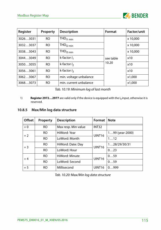
Modbus Register Map
Tab. 10.19: Minimum log of last month
1) Register 2972…2977 are valid only if the device is equipped with the I4 input, otherwise it is reserved.
10.8.5 Max/Min log data structure
Tab. 10.20: Max/Min log data structure
3026…3031 RO THDI1 min
see table 10.20
x 10,000
3032…3037 RO THDI2 min x 10,000
3038…3043 RO THDI3 min x 10,000
3044…3049 RO k-factor I1 x10
3050…3055 RO k-factor I2 x10
3056…3061 RO k-factor I3 x10
3062…3067 RO min. voltage unbalance x1,000
3068…3073 RO min. current unbalance x1,000
Offset Property Description Format Note
+ 0 RO Max resp. Min value INT32
+ 2RO HiWord: Year
UINT161…99 (year-2000)
RO LoWord: Month 1…12
+ 3RO HiWord: Date: Day
UINT161…28/29/30/31
RO LoWord: Hour 0…23
+ 4RO HiWord: Minute
UINT160…59
RO LoWord: Second 0…59
+ 5 RO Millisecond UINT16 0…999
Register Property Description Format Factor/unit
115PEM575_D00016_01_M_XXEN/05.2016
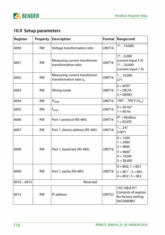
Modbus Register Map
10.9 Setup parameters
Register Property Description Format Range/unit
6000 RW Voltage transformation ratio UINT161*…10,000
6001 RWMeasuring current transformer transformation ratio
UINT16
1*…6,000 (current input 5 A) 1*…30,000(current input 1 A)
6002 RWMeasuring current transformer transformation ratio I4
UINT161…10,000(2*)
6003 RW Wiring mode UINT160 = WYE*1 = DELTA 2 = DEMO
6004 RW Unom UINT16 100*…700 V (ULL)
6005 RW fnom UINT160 = 50 Hz*1 = 60 Hz
6006 RW Port 1 protocol (RS-485) UINT160* = Modbus1 = EGATE
6007 RW Port 1, device address (RS-485) UINT161…247 (100*)
6008 RW Port 1, baud rate (RS-485) UINT16
0 = 1200 1 = 2400 2 = 4800 3 = 9600* 4 = 192005 = 38,400
6009 RW Port 1, parity (RS-485) UINT160 = 8N2; 1 = 8O1 2 = 8E1* ; 3 = 8N1 4 = 8O2 ; 5 = 8E2
6010…6012 Reserved
6013 RW IP address UINT32
192.168.8.97*Contents of register for factory setting:0xC0A80861
116 PEM575_D00016_01_M_XXEN/05.2016
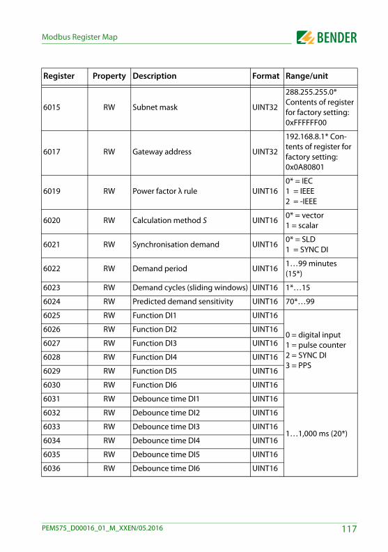
Modbus Register Map
6015 RW Subnet mask UINT32
288.255.255.0*Contents of register for factory setting:0xFFFFFF00
6017 RW Gateway address UINT32
192.168.8.1* Con-tents of register for factory setting:0x0A80801
6019 RW Power factor λ rule UINT160* = IEC 1 = IEEE 2 = -IEEE
6020 RW Calculation method S UINT160* = vector 1 = scalar
6021 RW Synchronisation demand UINT160* = SLD1 = SYNC DI
6022 RW Demand period UINT161…99 minutes(15*)
6023 RW Demand cycles (sliding windows) UINT16 1*…15
6024 RW Predicted demand sensitivity UINT16 70*…99
6025 RW Function DI1 UINT16
0 = digital input1 = pulse counter2 = SYNC DI3 = PPS
6026 RW Function DI2 UINT16
6027 RW Function DI3 UINT16
6028 RW Function DI4 UINT16
6029 RW Function DI5 UINT16
6030 RW Function DI6 UINT16
6031 RW Debounce time DI1 UINT16
1…1,000 ms (20*)
6032 RW Debounce time DI2 UINT16
6033 RW Debounce time DI3 UINT16
6034 RW Debounce time DI4 UINT16
6035 RW Debounce time DI5 UINT16
6036 RW Debounce time DI6 UINT16
Register Property Description Format Range/unit
117PEM575_D00016_01_M_XXEN/05.2016
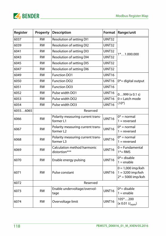
Modbus Register Map
6037 RW Resolution of setting DI1 UINT32
1*…1.000.000
6039 RW Resolution of setting DI2 UINT32
6041 RW Resolution of setting DI3 UINT32
6043 RW Resolution of setting DI4 UINT32
6045 RW Resolution of setting DI5 UINT32
6047 RW Resolution of setting DI6 UINT32
6049 RW Function DO1 UINT16
0*= digital output6050 RW Function DO2 UINT16
6051 RW Function DO3 UINT16
6052 RW Pulse width DO1 UINT16 0…999 (x 0.1 s)0 = Latch mode(10*)
6053 RW Pulse width DO2 UINT16
6054 RW Pulse width DO3 UINT16
6055…6065 Reserved
6066 RWPolarity measuring current trans-former L1
UINT160* = normal1 = reversed
6067 RWPolarity measuring current trans-former L2
UINT160* = normal 1 = reversed
6068 RWPolarity measuring current trans-former L3
UINT160* = normal 1 = reversed
6069 RWCalculation method harmonic distortion***
UINT160 = Fundamental1*= RMS
6070 RW Enable energy pulsing UINT160*= disable1 = enable
6071 RW Pulse constant UINT160 = 1,000 imp/kxh1 = 3200 imp/kxh2* = 5000 imp/kxh
6072 Reserved
6073 RWEnable undervoltage/overvol-tage
UINT160*= disable1 = enable
6074 RW Overvoltage limit UINT16105*…200 (x 0.01 Unom)
Register Property Description Format Range/unit
118 PEM575_D00016_01_M_XXEN/05.2016
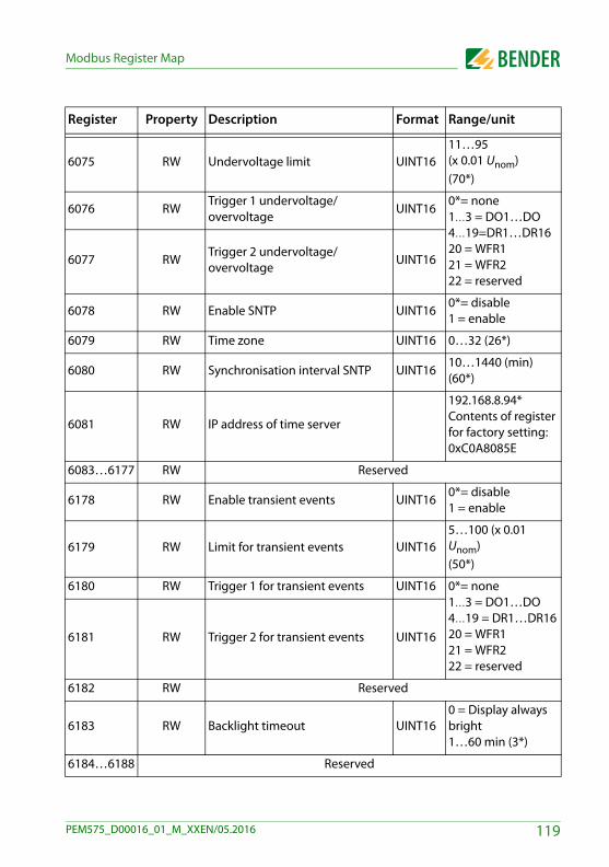
Modbus Register Map
6075 RW Undervoltage limit UINT1611…95 (x 0.01 Unom)(70*)
6076 RWTrigger 1 undervoltage/overvoltage
UINT160*= none1…3 = DO1…DO4…19=DR1…DR1620 = WFR121 = WFR222 = reserved
6077 RWTrigger 2 undervoltage/overvoltage
UINT16
6078 RW Enable SNTP UINT160*= disable1 = enable
6079 RW Time zone UINT16 0…32 (26*)
6080 RW Synchronisation interval SNTP UINT1610…1440 (min) (60*)
6081 RW IP address of time server
192.168.8.94*Contents of register for factory setting:0xC0A8085E
6083…6177 RW Reserved
6178 RW Enable transient events UINT160*= disable1 = enable
6179 RW Limit for transient events UINT165…100 (x 0.01 Unom)(50*)
6180 RW Trigger 1 for transient events UINT16 0*= none1…3 = DO1…DO4…19 = DR1…DR1620 = WFR121 = WFR222 = reserved
6181 RW Trigger 2 for transient events UINT16
6182 RW Reserved
6183 RW Backlight timeout UINT160 = Display always bright1…60 min (3*)
6184…6188 Reserved
Register Property Description Format Range/unit
119PEM575_D00016_01_M_XXEN/05.2016

Modbus Register Map
Tab. 10.21: Setup parameters
Notes table 10.21:Register 6000 and 6001
Current input 5 A: Transformation ratio current x transformation ratio voltage < 1,000,000Current input 1 A: Transformation ratio current x transformation ratio voltage < 5,000,000
Register 6078 is disabled if not equipped with an Ethernet port
120 PEM575_D00016_01_M_XXEN/05.2016

Modbus Register Map
Register 6079: Time zones without summertime
10.10 Clear/reset register
CODE Time zone CODE Time zone
0 GMT – 12 h 17 GMT + 03:30 h
1 GMT - 11 h 18 GMT + 04 h
2 GMT - 10 h 19 GMT + 04:30 h
3 GMT - 09 h 20 GMT + 05 h
4 GMT - 08 h 21 GMT + 05:30 h
5 GMT - 07 h 22 GMT + 05:45 h
6 GMT - 06 h 23 GMT + 06 h
7 GMT - 05 h 24 GMT + 06:30 h
8 GMT - 04 h 25 GMT + 07 h
9 GMT - 03 h 26 GMT + 08 h
10 GMT – 03:30 h 27 GMT + 09 h
11 GMT - 02 h 28 GMT + 09:30 h
12 GMT - 01 h 29 GMT + 10 h
13 GMT 30 GMT + 11 h
14 GMT + 01 h 31 GMT + 12 h
15 GMT + 02 h 32 GMT + 13 h
16 GMT + 03 h
Register Property Description Format Unit
6400 WO Manual WFR1 Trigger UINT16 Writing 0xFF00 to the register triggers the respective waveform recorder
6401 WO Manual WFR2 Trigger UINT16
6402 WO Clear DR1 (high speed) UINT16Writing 0xFF00 to the register clears the res-pective DR
121PEM575_D00016_01_M_XXEN/05.2016
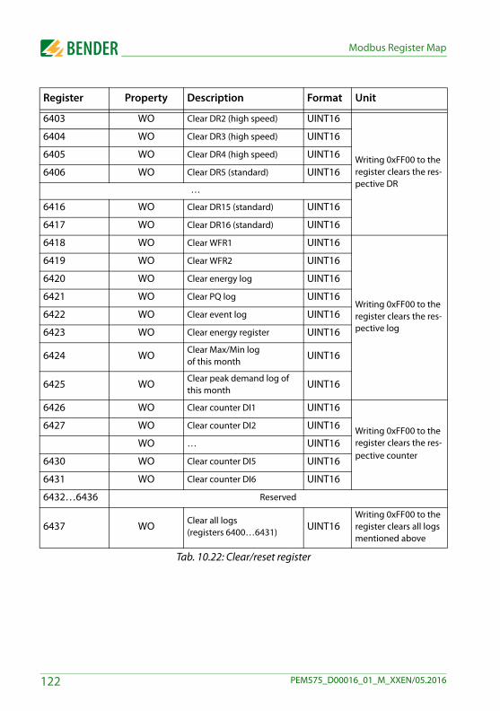
Modbus Register Map
Tab. 10.22: Clear/reset register
6403 WO Clear DR2 (high speed) UINT16
Writing 0xFF00 to the register clears the res-pective DR
6404 WO Clear DR3 (high speed) UINT16
6405 WO Clear DR4 (high speed) UINT16
6406 WO Clear DR5 (standard) UINT16
…
6416 WO Clear DR15 (standard) UINT16
6417 WO Clear DR16 (standard) UINT16
6418 WO Clear WFR1 UINT16
Writing 0xFF00 to the register clears the res-pective log
6419 WO Clear WFR2 UINT16
6420 WO Clear energy log UINT16
6421 WO Clear PQ log UINT16
6422 WO Clear event log UINT16
6423 WO Clear energy register UINT16
6424 WO Clear Max/Min log of this month
UINT16
6425 WO Clear peak demand log of this month
UINT16
6426 WO Clear counter DI1 UINT16
Writing 0xFF00 to the register clears the res-pective counter
6427 WO Clear counter DI2 UINT16
WO … UINT16
6430 WO Clear counter DI5 UINT16
6431 WO Clear counter DI6 UINT16
6432…6436 Reserved
6437 WO Clear all logs(registers 6400…6431)
UINT16Writing 0xFF00 to the register clears all logs mentioned above
Register Property Description Format Unit
122 PEM575_D00016_01_M_XXEN/05.2016
Modbus Register Map
10.11 Setpoint setup parameters
Tab. 10.23: Setpoints
Register Property Description Format
6600…6609 RW Setpoint 1 (standard)
Chapter 10.11.1 Struc-ture of the setpoint register (standard)
6610…6619 RW Setpoint 2 (standard)
6620…6629 RW Setpoint 3 (standard)
6630…6639 RW Setpoint 4 (standard)
6640…6649 RW Setpoint 5 (standard)
6650…6659 RW Setpoint 6 (standard)
6660…6669 RW Setpoint 7 (standard)
6670…6679 RW Setpoint 8 (standard)
6680…6689 RW Setpoint 9 (standard)
6690…6699 RW Setpoint 10 (standard)
6700…6709 RW Setpoint 11 (standard)
6710…6719 RW Setpoint 12 (standard)
6720…7629 RW Setpoint 13 (standard)
6730…6739 RW Setpoint 14 (standard)
6740…6749 RW Setpoint 15 (standard)
6750…6759 RW Setpoint 16 (standard)
6760…6769 RW Setpoint 17 (highspeed)
Chapter 10.11.2 Set-point register structure (high speed)
6770…6779 RW Setpoint 18 (highspeed)
6780…6789 RW Setpoint 19 (highspeed)
6790…6799 RW Setpoint 20 (highspeed)
6800…6809 RW Setpoint 21 (highspeed)
6810…6819 RW Setpoint 22 (highspeed)
6820…6829 RW Setpoint 23 (highspeed)
6830…6839 RW Setpoint 24 (highspeed)
123PEM575_D00016_01_M_XXEN/05.2016
Modbus Register Map
10.11.1 Structure of the setpoint register (standard)
Tab. 10.24: Setpoint register structure (standard)
10.11.2 Setpoint register structure (high speed)
Tab. 10.25: Setpoint register structure (high speed)
Offset Property Description Format Unit
0 RW Type UINT160 = disabled1 = over setpoint2 = under setpoint
+1 RW Measured quantity1) UINT16 1*…31
+2 RW Active limit INT32 5000*
+4 RW Inactive limit INT32 1,000*
+6 RW Active delay UINT16 0…9,999 s(1*)
+7 RW Inactive delay UINT16 0…9,999 s(1*)
+8 RW Trigger 1 2) UINT16 0…22 (1*)
+9 RW Trigger 2 2) UINT16 0…22 (2*)
Offset Property Description Format Unit
0 RW Type UINT160 = disabled1 = over setpoint2 = under setpoint
+1 RW Measured Quantity1) UINT16 1*…14
+2 RW Active limit INT32 5000*
+4 RW Inactive limit INT32 1,000*
+6 RW Active delay UINT16 0…9,999 cycles (1*)
+7 RW Inactive delay UINT16 0…9,999 cycles (1*)
+8 RW Trigger 1 2) UINT16 0…22 (1*)
+9 RW Trigger 2 2) UINT16 0…22 (2*)
124 PEM575_D00016_01_M_XXEN/05.2016
Modbus Register Map
Notes table 10.24 and table 10.25:1) Measured quantity: "Measured quantity" specifies the parameter to be monitored. The following
measured quantities can be set:
Setpoint parameter "Measured quantity"
Key Measured quantity Scale/unit
1 ULN x 100, V
2 ULL x 100, V
3 I x 1,000, A
4 I4 x 1,000, A
5 fΔn x 100, Hz
6 Pges kW
7 Qges kvar
8 λ x1,000
9 DI1Over setpoint:
active limit will close DI (DI = 1),inactive limit will open DI (DI = 0)
Under setpoint: active limit will open DI (DI = 0),inactive limit will close DI (DI = 1)
10 DI2
11 DI3
12 DI4
13 DI5
14 DI6
15 Reserved
16 Demand Pges kW
17 Demand Qges kvar
18 Demand λ x1,000
19 Predicted demand Pges kW
20 Predicted demand Qges kvar
21 Predicted demand λ x1,000
22 THDU x 10,000
23 TOHDU x 10,000
24 TEHDU x 10,000
125PEM575_D00016_01_M_XXEN/05.2016
Modbus Register Map
Tab. 10.26: Setpoint parameter
2) Trigger
The trigger specifies what action the setpoint will take when it becomes active.
Tab. 10.27: Setpoint trigger
25 THDI x 10,000
26 TOHDI x 10,000
27 TEHDI x 10,000
28 Unbalance U x1,000
29 Unbalance I x1,000
30 Deviation U x 10,000
31 Phase reversal
Over setpoint: active limit at negative phase sequence;inactive limit at positive phase sequenceUnder setpoint:active limit at positive phase sequence;inactive limit at negative phase sequence
Key Action Key Action Key Action
0 — 8 DR5 16 DR13
1 DO1 9 DR6 17 DR14
2 DO2 10 DR7 18 DR15
3 DO3 11 DR8 19 DR16
4 DR1 12 DR9 20 WFR1
5 DR2 13 DR10 21 WFR2
6 DR3 14 DR11 22 Reserved
7 DR4 15 DR12
Key Measured quantity Scale/unit
126 PEM575_D00016_01_M_XXEN/05.2016
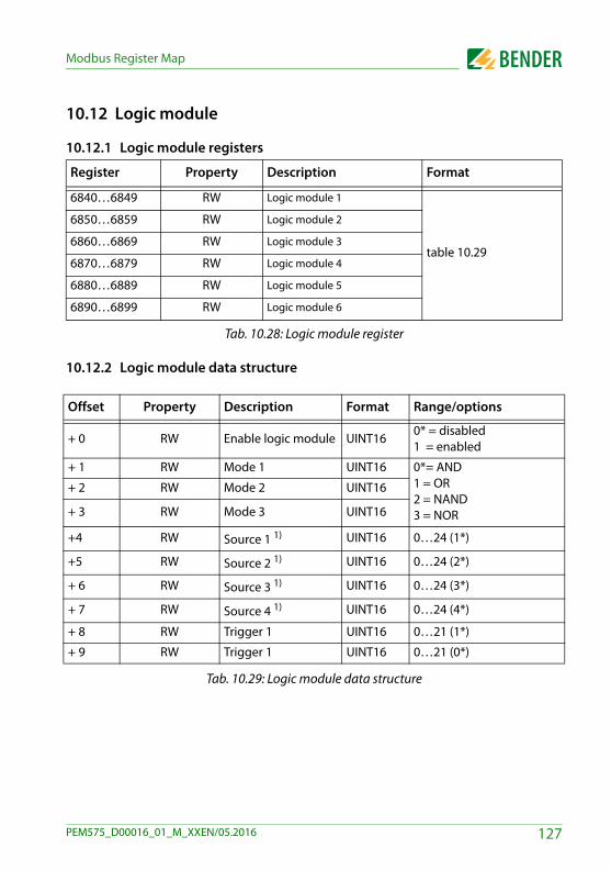
Modbus Register Map
10.12 Logic module
10.12.1 Logic module registers
Tab. 10.28: Logic module register
10.12.2 Logic module data structure
Tab. 10.29: Logic module data structure
Register Property Description Format
6840…6849 RW Logic module 1
table 10.29
6850…6859 RW Logic module 2
6860…6869 RW Logic module 3
6870…6879 RW Logic module 4
6880…6889 RW Logic module 5
6890…6899 RW Logic module 6
Offset Property Description Format Range/options
+ 0 RW Enable logic module UINT160* = disabled1 = enabled
+ 1 RW Mode 1 UINT16 0*= AND1 = OR2 = NAND3 = NOR
+ 2 RW Mode 2 UINT16
+ 3 RW Mode 3 UINT16
+4 RW Source 1 1) UINT16 0…24 (1*)
+5 RW Source 2 1) UINT16 0…24 (2*)
+ 6 RW Source 3 1) UINT16 0…24 (3*)
+ 7 RW Source 4 1) UINT16 0…24 (4*)
+ 8 RW Trigger 1 UINT16 0…21 (1*)
+ 9 RW Trigger 1 UINT16 0…21 (0*)
127PEM575_D00016_01_M_XXEN/05.2016
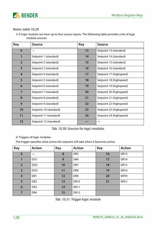
Modbus Register Map
Notes: table 10.291) A logic module can have up to four source inputs. The following table provides a list of logic
module sources:
Tab. 10.30: Sources for logic modules
2) Triggers of logic modules
The trigger specifies what action the setpoint will take when it becomes active.
Tab. 10.31: Trigger logic module
Key Source Key Source
0 — 13 Setpoint 13 (standard)
1 Setpoint 1 (standard) 14 Setpoint 14 (standard)
2 Setpoint 2 (standard) 15 Setpoint 15 (standard)
3 Setpoint 3 (standard) 16 Setpoint 16 (standard)
4 Setpoint 4 (standard) 17 Setpoint 17 (highspeed)
5 Setpoint 5 (standard) 18 Setpoint 18 (highspeed)
6 Setpoint 6 (standard) 19 Setpoint 19 (highspeed)
7 Setpoint 7 (standard) 20 Setpoint 20 (highspeed)
8 Setpoint 8 (standard) 21 Setpoint 21 (highspeed)
9 Setpoint 9 (standard) 22 Setpoint 22 (highspeed)
10 Setpoint 10 (standard) 23 Setpoint 23 (highspeed)
11 Setpoint 11 (standard) 24 Setpoint 24 (highspeed)
12 Setpoint 12 (standard) — —
Key Action Key Action Key Action
0 — 8 DR5 16 DR13
1 DO1 9 DR6 17 DR14
2 DO2 10 DR7 18 DR15
3 DO3 11 DR8 19 DR16
4 DR1 12 DR9 20 WFR1
5 DR2 13 DR10 21 WFR 2
6 DR3 14 DR11
7 DR4 15 DR12
128 PEM575_D00016_01_M_XXEN/05.2016
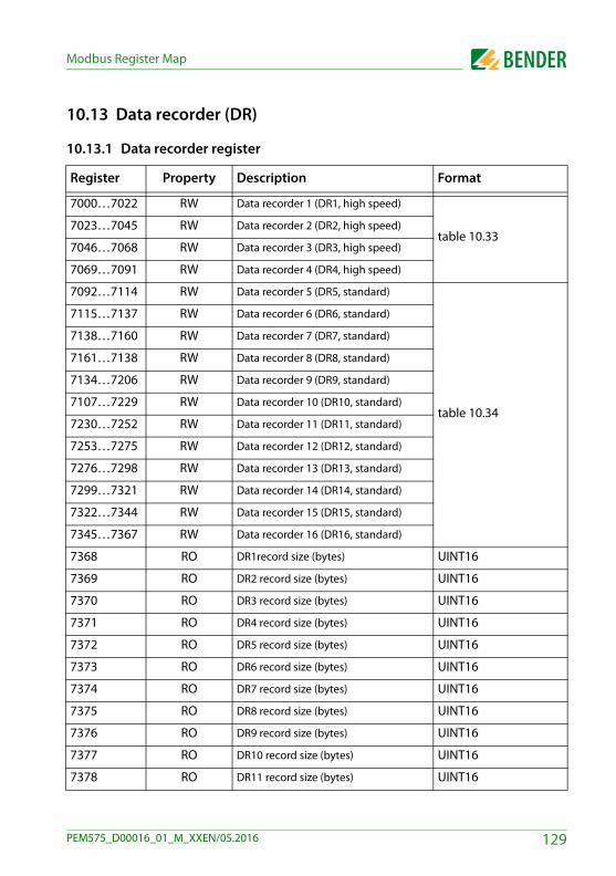
Modbus Register Map
10.13 Data recorder (DR)
10.13.1 Data recorder register
Register Property Description Format
7000…7022 RW Data recorder 1 (DR1, high speed)
table 10.33 7023…7045 RW Data recorder 2 (DR2, high speed)
7046…7068 RW Data recorder 3 (DR3, high speed)
7069…7091 RW Data recorder 4 (DR4, high speed)
7092…7114 RW Data recorder 5 (DR5, standard)
table 10.34
7115…7137 RW Data recorder 6 (DR6, standard)
7138…7160 RW Data recorder 7 (DR7, standard)
7161…7138 RW Data recorder 8 (DR8, standard)
7134…7206 RW Data recorder 9 (DR9, standard)
7107…7229 RW Data recorder 10 (DR10, standard)
7230…7252 RW Data recorder 11 (DR11, standard)
7253…7275 RW Data recorder 12 (DR12, standard)
7276…7298 RW Data recorder 13 (DR13, standard)
7299…7321 RW Data recorder 14 (DR14, standard)
7322…7344 RW Data recorder 15 (DR15, standard)
7345…7367 RW Data recorder 16 (DR16, standard)
7368 RO DR1record size (bytes) UINT16
7369 RO DR2 record size (bytes) UINT16
7370 RO DR3 record size (bytes) UINT16
7371 RO DR4 record size (bytes) UINT16
7372 RO DR5 record size (bytes) UINT16
7373 RO DR6 record size (bytes) UINT16
7374 RO DR7 record size (bytes) UINT16
7375 RO DR8 record size (bytes) UINT16
7376 RO DR9 record size (bytes) UINT16
7377 RO DR10 record size (bytes) UINT16
7378 RO DR11 record size (bytes) UINT16
129PEM575_D00016_01_M_XXEN/05.2016
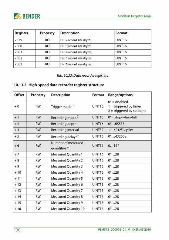
Modbus Register Map
Tab. 10.32: Data recorder registers
10.13.2 High-speed data recorder register structure
7379 RO DR12 record size (bytes) UINT16
7380 RO DR13 record size (bytes) UINT16
7381 RO DR14 record size (bytes) UINT16
7382 RO DR15 record size (bytes) UINT16
7383 RO DR16 record size (bytes) UINT16
Offset Property Description Format Range/options
+ 0 RW Trigger mode 1) UINT160* = disabled1 = triggered by timer2 = triggered by setpoint
+ 1 RW Recording mode 2) UINT16 0*= stop-when-full
+ 2 RW Recording depth UINT16 0*…65535
+ 3 RW Recording interval UINT32 1…60 (2*) cycles
+ 5 RW Recording delay 3) UINT16 0*…43200 s
+ 6 RWNumber of measured quantities 4) UINT16 0…16*
+ 7 RW Measured Quantity 1 UINT16 0*…28
+ 8 RW Measured Quantity 2 UINT16 0*…28
+ 9 RW Measured Quantity 3 UINT16 0*…28
+ 10 RW Measured Quantity 4 UINT16 0*…28
+ 11 RW Measured Quantity 5 UINT16 0*…28
+ 12 RW Measured Quantity 6 UINT16 0*…28
+ 13 RW Measured Quantity 7 UINT16 0*…28
+ 14 RW Measured Quantity 8 UINT16 0*…28
+ 15 RW Measured Quantity 9 UINT16 0*…28
+ 16 RW Measured Quantity 10 UINT16 0*…28
Register Property Description Format
130 PEM575_D00016_01_M_XXEN/05.2016
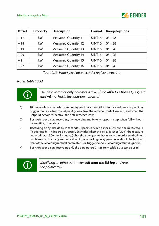
Modbus Register Map
Tab. 10.33: High-speed data recorder register structure
Notes: table 10.33
1) High-speed data recorders can be triggered by a timer (the internal clock) or a setpoint. In trigger mode 2 when the setpoint goes active, the recorder starts to record, and when the setpoint becomes inactive, the data recorder stops.
2) For high-speed data recorders, the recording mode only supports stop-when-full without overwriting other data.
3) Recording delay: The delay in seconds is specified when a measurement is to be started in Trigger mode 1 (triggered by timer). Example: When the delay is set to "300", the measure-ment will start 300 s (= 5 minutes) after the timer period has elapsed. In order to obtain eval-uable results, the programmed value of the recording delay parameter should be less than that of the recording interval parameter. For Trigger mode 2, recording offset is ignored.
4) For high-speed data recorders only the parameters 0…28 from table 8.3.2 can be used.
+ 17 RW Measured Quantity 11 UINT16 0*…28
+ 18 RW Measured Quantity 12 UINT16 0*…28
+ 19 RW Measured Quantity 13 UINT16 0*…28
+ 20 RW Measured Quantity 14 UINT16 0*…28
+ 21 RW Measured Quantity 15 UINT16 0*…28
+ 22 RW Measured Quantity 16 UINT16 0*…28
The data recorder only becomes active, if the offset entries +1, +2, +3and +6 marked in the table are non-zero!
Modifying an offset parameter will clear the DR log and reset the pointer to 0.
Offset Property Description Format Range/options
131PEM575_D00016_01_M_XXEN/05.2016
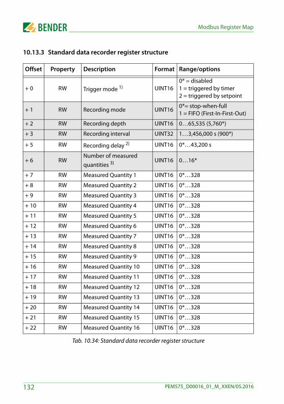
Modbus Register Map
10.13.3 Standard data recorder register structure
Tab. 10.34: Standard data recorder register structure
Offset Property Description Format Range/options
+ 0 RW Trigger mode 1) UINT160* = disabled1 = triggered by timer2 = triggered by setpoint
+ 1 RW Recording mode UINT160*= stop-when-full1 = FIFO (First-In-First-Out)
+ 2 RW Recording depth UINT16 0…65,535 (5,760*)
+ 3 RW Recording interval UINT32 1…3,456,000 s (900*)
+ 5 RW Recording delay 2) UINT16 0*…43,200 s
+ 6 RWNumber of measured quantities 3) UINT16 0…16*
+ 7 RW Measured Quantity 1 UINT16 0*…328
+ 8 RW Measured Quantity 2 UINT16 0*…328
+ 9 RW Measured Quantity 3 UINT16 0*…328
+ 10 RW Measured Quantity 4 UINT16 0*…328
+ 11 RW Measured Quantity 5 UINT16 0*…328
+ 12 RW Measured Quantity 6 UINT16 0*…328
+ 13 RW Measured Quantity 7 UINT16 0*…328
+ 14 RW Measured Quantity 8 UINT16 0*…328
+ 15 RW Measured Quantity 9 UINT16 0*…328
+ 16 RW Measured Quantity 10 UINT16 0*…328
+ 17 RW Measured Quantity 11 UINT16 0*…328
+ 18 RW Measured Quantity 12 UINT16 0*…328
+ 19 RW Measured Quantity 13 UINT16 0*…328
+ 20 RW Measured Quantity 14 UINT16 0*…328
+ 21 RW Measured Quantity 15 UINT16 0*…328
+ 22 RW Measured Quantity 16 UINT16 0*…328
132 PEM575_D00016_01_M_XXEN/05.2016
Modbus Register Map
Notes: table 10.34
1) The standard data recorder can be triggered by a Timer (the internal clock) or by Setpoint. In trigger mode 2 when the setpoint goes active, the recorder starts to record, and when the setpoint becomes inactive, the data recorder stops.
2) Recording delay: In Trigger mode 1, a fixed time can be set in seconds to delay the start of the measurement (triggered by timer). Example: When the delay is set to "300", the measure-ment will start 300 s (= 5 minutes) after the timer period has elapsed. In order to obtain eval-uable results, the programmed value of the recording delay parameter should be less than that of the recording interval parameter. For Trigger mode 2, recording delay is ignored.
3) For standard data recorders all the measured quantities 0…328 from table 8.3.2 can be used.
10.14 Waveform recording (WFR)The PEM575 provides two waveform recorders capable of recording waveforms independently from one another (waveform recorder WFR1 and WFR2). The total capacity of WRF 1 and WFR 2 is 32.
The data recorder is only operational when the offset entries +1, +2, +3and +6 are all non-zero!
Modifying an offset parameter will clear the DR log and reset the pointerto 0.
133PEM575_D00016_01_M_XXEN/05.2016
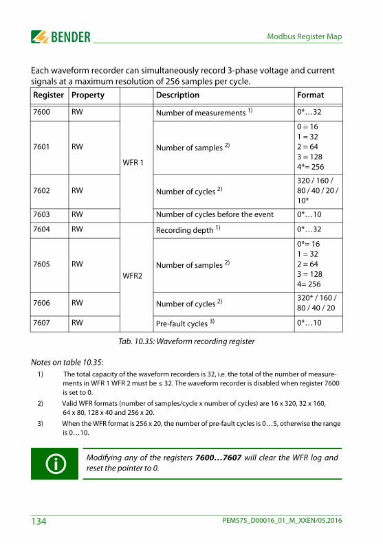
Modbus Register Map
Each waveform recorder can simultaneously record 3-phase voltage and current signals at a maximum resolution of 256 samples per cycle.
Tab. 10.35: Waveform recording register
Notes on table 10.35: 1) The total capacity of the waveform recorders is 32, i.e. the total of the number of measure-
ments in WFR 1 WFR 2 must be ≤ 32. The waveform recorder is disabled when register 7600 is set to 0.
2) Valid WFR formats (number of samples/cycle x number of cycles) are 16 x 320, 32 x 160, 64 x 80, 128 x 40 and 256 x 20.
3) When the WFR format is 256 x 20, the number of pre-fault cycles is 0…5, otherwise the range is 0…10.
Register Property Description Format
7600 RW
WFR 1
Number of measurements 1) 0*…32
7601 RW Number of samples 2)
0 = 161 = 32 2 = 643 = 1284*= 256
7602 RW Number of cycles 2) 320 / 160 / 80 / 40 / 20 / 10*
7603 RW Number of cycles before the event 0*…10
7604 RW
WFR2
Recording depth 1) 0*…32
7605 RW Number of samples 2)
0*= 161 = 32 2 = 643 = 1284= 256
7606 RW Number of cycles 2) 320* / 160 / 80 / 40 / 20
7607 RW Pre-fault cycles 3) 0*…10
Modifying any of the registers 7600…7607 will clear the WFR log andreset the pointer to 0.
134 PEM575_D00016_01_M_XXEN/05.2016
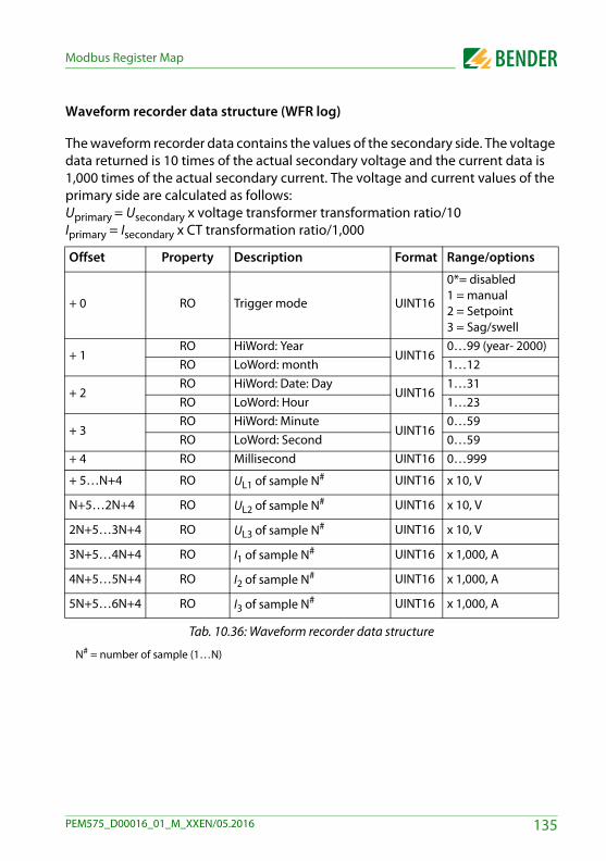
Modbus Register Map
Waveform recorder data structure (WFR log)
The waveform recorder data contains the values of the secondary side. The voltage data returned is 10 times of the actual secondary voltage and the current data is 1,000 times of the actual secondary current. The voltage and current values of the primary side are calculated as follows:Uprimary = Usecondary x voltage transformer transformation ratio/10Iprimary = Isecondary x CT transformation ratio/1,000
Tab. 10.36: Waveform recorder data structure
N# = number of sample (1…N)
Offset Property Description Format Range/options
+ 0 RO Trigger mode UINT16
0*= disabled1 = manual2 = Setpoint3 = Sag/swell
+ 1RO HiWord: Year
UINT160…99 (year- 2000)
RO LoWord: month 1…12
+ 2RO HiWord: Date: Day
UINT161…31
RO LoWord: Hour 1…23
+ 3RO HiWord: Minute
UINT160…59
RO LoWord: Second 0…59+ 4 RO Millisecond UINT16 0…999
+ 5…N+4 RO UL1 of sample N# UINT16 x 10, V
N+5…2N+4 RO UL2 of sample N# UINT16 x 10, V
2N+5…3N+4 RO UL3 of sample N# UINT16 x 10, V
3N+5…4N+4 RO I1 of sample N# UINT16 x 1,000, A
4N+5…5N+4 RO I2 of sample N# UINT16 x 1,000, A
5N+5…6N+4 RO I3 of sample N# UINT16 x 1,000, A
135PEM575_D00016_01_M_XXEN/05.2016
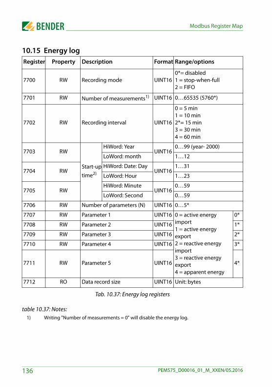
Modbus Register Map
10.15 Energy log
Tab. 10.37: Energy log registers
table 10.37: Notes:1) Writing "Number of measurements = 0" will disable the energy log.
Register Property Description Format Range/options
7700 RW Recording mode UINT160*= disabled1 = stop-when-full2 = FIFO
7701 RW Number of measurements1) UINT16 0…65535 (5760*)
7702 RW Recording interval UINT16
0 = 5 min1 = 10 min2*= 15 min3 = 30 min4 = 60 min
7703 RW
Start-up time2)
HiWord: YearUINT16
0…99 (year- 2000)
LoWord: month 1…12
7704 RWHiWord: Date: Day
UINT161…31
LoWord: Hour 1…23
7705 RWHiWord: Minute
UINT160…59
LoWord: Second 0…59
7706 RW Number of parameters (N) UINT16 0…5*
7707 RW Parameter 1 UINT16 0 = active energy import1 = active energy export2 = reactive energy import3 = reactive energy export4 = apparent energy
0*
7708 RW Parameter 2 UINT16 1*
7709 RW Parameter 3 UINT16 2*
7710 RW Parameter 4 UINT16 3*
7711 RW Parameter 5 UINT16 4*
7712 RO Data record size UINT16 Unit: bytes
136 PEM575_D00016_01_M_XXEN/05.2016

Modbus Register Map
2) When the current time meets or exceeds the start-up time, the energy log starts to record.
Energy log data structure
Tab. 10.38: Energy log data structure
Modifying any of the registers 7701…7711 will clear the Energy log andreset the pointer to 0.
Offset Property Description Format Range/options
+0 RO Parameter 1 INT32
+2 RO Parameter 2 INT32
… RO … INT32
+2N ROParameter N (N = 0…5)
INT32
+2N+1 ROHiWord: Year
UINT160…99 (year - 2000)
LoWord: month 1…12
+2N+2 ROHiWord: Date: Day
UINT161…31
LoWord: Hour 1…23
+2N+3 ROHiWord: Minute
UINT160…59
LoWord: Second 0…59
+2N+4 RO Millisecond UINT16 0…999
137PEM575_D00016_01_M_XXEN/05.2016
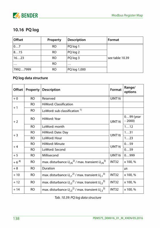
Modbus Register Map
10.16 PQ log
PQ log data structure
Tab. 10.39: PQ log data structure
Offset Property Description Format
0…7 RO PQ log 1
see table 10.39
8…15 RO PQ log 2
16…23 RO PQ log 3
… RO …
7992…7999 RO PQ log 1,000
Offset Property Description Format Range/options
+ 0 RO Reserved UINT16
+ 1RO HiWord: Classification
RO LoWord: sub classification 1)
+ 2RO HiWord: Year
UINT160…99 (year – 2000)
RO LoWord: month 1…12
+ 3RO HiWord: Date: Day
UINT161…31
RO LoWord: Hour 1…23
+ 4 RO HiWord: Minute
UINT160…59
RO LoWord: Second 0…59
+ 5 RO Millisecond UINT16 0…999
+ 6 4) RO max. disturbance ULN2) / max. transient ULN
3) INT32 x 100, %
+ 8 RO Duration μs
+ 10 RO max. disturbance UL12) / max. transient UL1
3) INT32 x 100, %
+ 12 RO max. disturbance UL22) / max. transient UL2
3) INT32 x 100, %
+ 14 RO max. disturbance UL32) / max. transient UL3
3) INT32 x 100, %
138 PEM575_D00016_01_M_XXEN/05.2016
Modbus Register Map
Notes table 10.39: 1) The PQ log classification is "7".
The following sub classifications are used:
2) Sag/swell inactive value: max. value of disturbance ULx ULx = ((ULx max - ULx nenn) / ULx nenn ) x 100 % (with Lx = L1…L3)
Max. disturbance ULN is the maximum value of max. disturbance ULx
3) Transient events: ULx transient max = (ULx max / Unenn) x 100 % (with Lx = L1…L3)
Max. ULN transient is the maximum value of ULx transient
4) For sag/swell events, the offsets + 6…+ 14 are reserved.
10.17 Event log (SOE log)Each SOE event occupies 8 registers, as shown in the following table. The internal data structure of the event log is listed in table 10.41.
Sub classification Description
1 Start: sag/swell event
2 End: sag/swell event
3 Transient event
139PEM575_D00016_01_M_XXEN/05.2016
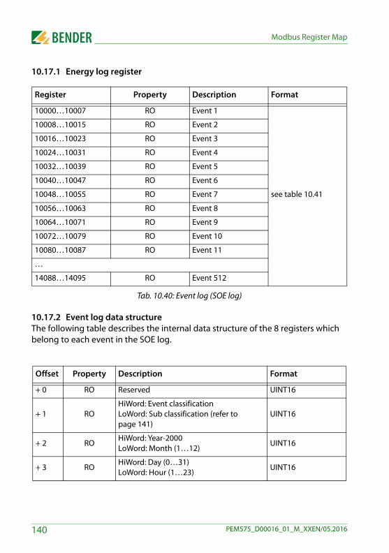
Modbus Register Map
10.17.1 Energy log register
Tab. 10.40: Event log (SOE log)
10.17.2 Event log data structureThe following table describes the internal data structure of the 8 registers which belong to each event in the SOE log.
Register Property Description Format
10000…10007 RO Event 1
see table 10.41
10008…10015 RO Event 2
10016…10023 RO Event 3
10024…10031 RO Event 4
10032…10039 RO Event 5
10040…10047 RO Event 6
10048…10055 RO Event 7
10056…10063 RO Event 8
10064…10071 RO Event 9
10072…10079 RO Event 10
10080…10087 RO Event 11
…
14088…14095 RO Event 512
Offset Property Description Format
+ 0 RO Reserved UINT16
+ 1 ROHiWord: Event classificationLoWord: Sub classification (refer to page 141)
UINT16
+ 2 ROHiWord: Year-2000LoWord: Month (1…12)
UINT16
+ 3 ROHiWord: Day (0…31)LoWord: Hour (1…23)
UINT16
140 PEM575_D00016_01_M_XXEN/05.2016

Modbus Register Map
Tab. 10.41: Event data structure
10.17.3 Event classification (SOE log)
+ 4 ROHiWord: M inute (0…59)LoWord: Second (0…59)
UINT16
+ 5 RO Millisecond (0…999) UINT16
+ 6 RO Event value INT32
Event classification
Event sub classification
Event valueUnit
OptionDescription
1
1 1/0 DI1 close/open
2 1/0 DI2 close/open
3 1/0 DI3 close/open
4 1/0 DI4 close/open
5 1/0 DI5 close/open
6 1/0 DI6 close/open
2
11/0
DO 1 close/open by communications interface
21/0
DO2 close/open by communications interface
31/0
DO3 close/open by communications interface
4 1/0 DO1 close/open by setpoint
5 1/0 DO2 close/open by setpoint
6 1/0 DO3 close/open by setpoint
71/0
DO1 close/open by undervoltage/over-voltage
81/0
DO2 close/open by undervoltage/over-voltage
91/0
DO3 close/open by undervoltage/over-voltage
Offset Property Description Format
141PEM575_D00016_01_M_XXEN/05.2016
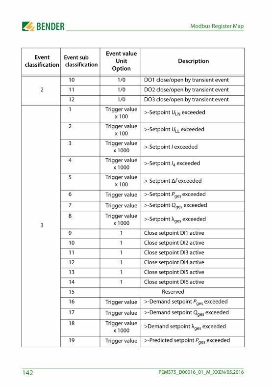
Modbus Register Map
2
10 1/0 DO1 close/open by transient event
11 1/0 DO2 close/open by transient event
12 1/0 DO3 close/open by transient event
3
1 Trigger value x 100
>-Setpoint ULN exceeded
2 Trigger value x 100
>-Setpoint ULL exceeded
3 Trigger value x 1000
>-Setpoint I exceeded
4 Trigger value x 1000
>-Setpoint I4 exceeded
5 Trigger value x 100
>-Setpoint Δf exceeded
6 Trigger value >-Setpoint Pges exceeded
7 Trigger value >-Setpoint Qges exceeded
8 Trigger value x 1000
>-Setpoint λges exceeded
9 1 Close setpoint DI1 active
10 1 Close setpoint DI2 active
11 1 Close setpoint DI3 active
12 1 Close setpoint DI4 active
13 1 Close setpoint DI5 active
14 1 Close setpoint DI6 active
15 Reserved
16 Trigger value >-Demand setpoint Pges exceeded
17 Trigger value >-Demand setpoint Qges exceeded
18 Trigger value x 1000
>Demand setpoint λges exceeded
19 Trigger value >-Predicted setpoint Pges exceeded
Event classification
Event sub classification
Event valueUnit
OptionDescription
142 PEM575_D00016_01_M_XXEN/05.2016
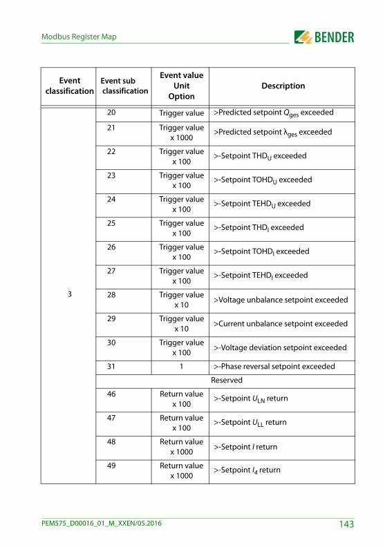
Modbus Register Map
3
20 Trigger value >Predicted setpoint Qges exceeded
21 Trigger value x 1000
>Predicted setpoint λges exceeded
22 Trigger value x 100
>-Setpoint THDU exceeded
23 Trigger value x 100
>-Setpoint TOHDU exceeded
24 Trigger value x 100
>-Setpoint TEHDU exceeded
25 Trigger value x 100
>-Setpoint THDI exceeded
26 Trigger value x 100
>-Setpoint TOHDI exceeded
27 Trigger value x 100
>-Setpoint TEHDI exceeded
28 Trigger value x 10
>Voltage unbalance setpoint exceeded
29 Trigger value x 10
>Current unbalance setpoint exceeded
30 Trigger value x 100
>-Voltage deviation setpoint exceeded
31 1 >-Phase reversal setpoint exceeded
Reserved
46 Return value x 100
>-Setpoint ULN return
47 Return value x 100
>-Setpoint ULL return
48 Return value x 1000
>-Setpoint I return
49 Return value x 1000
>-Setpoint I4 return
Event classification
Event sub classification
Event valueUnit
OptionDescription
143PEM575_D00016_01_M_XXEN/05.2016
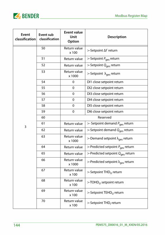
Modbus Register Map
3
50 Return value x 100
>-Setpoint Δf return
51 Return value >-Setpoint Pges return
52 Return value >-Setpoint Qges return
53 Return value x 1000
>-Setpoint λges return
54 0 DI1 close setpoint return
55 0 DI2 close setpoint return
56 0 DI3 close setpoint return
57 0 DI4 close setpoint return
58 0 DI5 close setpoint return
59 0 DI6 close setpoint return
60 Reserved
61 Return value >- Setpoint demand Pges return
62 Return value >-Setpoint demand Qges return
63 Return value x 1000
>-Demand setpoint λges return
64 Return value >-Predicted setpoint Pges return
65 Return value >-Predicted setpoint Qges return
66 Return value x 1000
>-Predicted setpoint λges return
67 Return value x 100
>-Setpoint THDU return
68 Return value x 100
>-TOHDU setpoint return
69 Return value x 100
>-Setpoint TEHDU return
70 Return value x 100
>-Setpoint THDI return
Event classification
Event sub classification
Event valueUnit
OptionDescription
144 PEM575_D00016_01_M_XXEN/05.2016
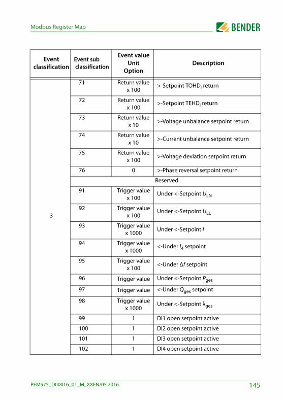
Modbus Register Map
3
71 Return value x 100
>-Setpoint TOHDI return
72 Return value x 100
>-Setpoint TEHDI return
73 Return value x 10
>-Voltage unbalance setpoint return
74 Return value x 10
>-Current unbalance setpoint return
75 Return value x 100
>-Voltage deviation setpoint return
76 0 >-Phase reversal setpoint return
Reserved
91 Trigger value x 100
Under <-Setpoint ULN
92 Trigger value x 100
Under <-Setpoint ULL
93 Trigger value x 1000
Under <-Setpoint I
94 Trigger value x 1000
<-Under I4 setpoint
95 Trigger value x 100
<-Under Δf setpoint
96 Trigger value Under <-Setpoint Pges
97 Trigger value <-Under Qges setpoint
98 Trigger value x 1000
Under <-Setpoint λges
99 1 DI1 open setpoint active
100 1 DI2 open setpoint active
101 1 DI3 open setpoint active
102 1 DI4 open setpoint active
Event classification
Event sub classification
Event valueUnit
OptionDescription
145PEM575_D00016_01_M_XXEN/05.2016
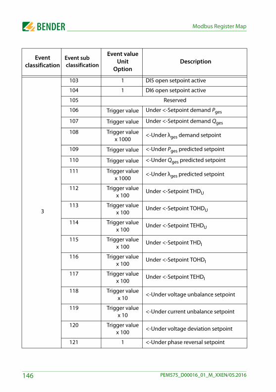
Modbus Register Map
3
103 1 DI5 open setpoint active
104 1 DI6 open setpoint active
105 Reserved
106 Trigger value Under <-Setpoint demand Pges
107 Trigger value Under <-Setpoint demand Qges
108 Trigger value x 1000
<-Under λges demand setpoint
109 Trigger value <-Under Pges predicted setpoint
110 Trigger value <-Under Qges predicted setpoint
111 Trigger value x 1000
<-Under λges predicted setpoint
112 Trigger value x 100
Under <-Setpoint THDU
113 Trigger value x 100
Under <-Setpoint TOHDU
114 Trigger value x 100
Under <-Setpoint TEHDU
115 Trigger value x 100
Under <-Setpoint THDI
116 Trigger value x 100
Under <-Setpoint TOHDI
117 Trigger value x 100
Under <-Setpoint TEHDI
118 Trigger value x 10
<-Under voltage unbalance setpoint
119 Trigger value x 10
<-Under current unbalance setpoint
120 Trigger value x 100
<-Under voltage deviation setpoint
121 1 <-Under phase reversal setpoint
Event classification
Event sub classification
Event valueUnit
OptionDescription
146 PEM575_D00016_01_M_XXEN/05.2016
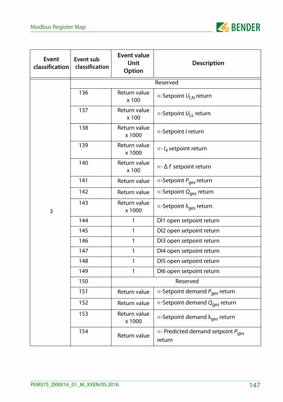
Modbus Register Map
3
Reserved
136 Return value x 100
<-Setpoint ULN return
137 Return value x 100
<-Setpoint ULL return
138 Return value x 1000
<-Setpoint I return
139 Return value x 1000
<- I4 setpoint return
140 Return value x 100
<- Δ f setpoint return
141 Return value <-Setpoint Pges return
142 Return value <-Setpoint Qges return
143 Return value x 1000
<-Setpoint λges return
144 1 DI1 open setpoint return
145 1 DI2 open setpoint return
146 1 DI3 open setpoint return
147 1 DI4 open setpoint return
148 1 DI5 open setpoint return
149 1 DI6 open setpoint return
150 Reserved
151 Return value <-Setpoint demand Pges return
152 Return value <-Setpoint demand Qges return
153 Return value x 1000
<-Setpoint demand λges return
154Return value
<- Predicted demand setpoint Pges return
Event classification
Event sub classification
Event valueUnit
OptionDescription
147PEM575_D00016_01_M_XXEN/05.2016
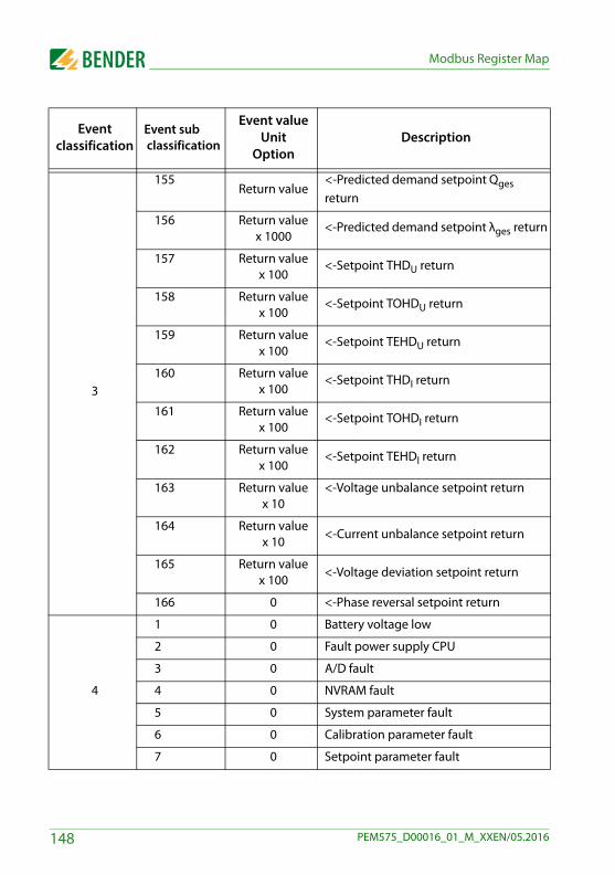
Modbus Register Map
3
155Return value
<-Predicted demand setpoint Qges return
156 Return value x 1000
<-Predicted demand setpoint λges return
157 Return value x 100
<-Setpoint THDU return
158 Return value x 100
<-Setpoint TOHDU return
159 Return value x 100
<-Setpoint TEHDU return
160 Return value x 100
<-Setpoint THDI return
161 Return value x 100
<-Setpoint TOHDI return
162 Return value x 100
<-Setpoint TEHDI return
163 Return value x 10
<-Voltage unbalance setpoint return
164 Return value x 10
<-Current unbalance setpoint return
165 Return value x 100
<-Voltage deviation setpoint return
166 0 <-Phase reversal setpoint return
4
1 0 Battery voltage low
2 0 Fault power supply CPU
3 0 A/D fault
4 0 NVRAM fault
5 0 System parameter fault
6 0 Calibration parameter fault
7 0 Setpoint parameter fault
Event classification
Event sub classification
Event valueUnit
OptionDescription
148 PEM575_D00016_01_M_XXEN/05.2016
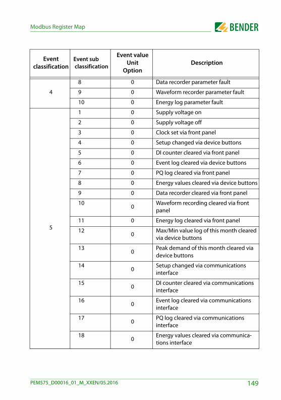
Modbus Register Map
4
8 0 Data recorder parameter fault
9 0 Waveform recorder parameter fault
10 0 Energy log parameter fault
5
1 0 Supply voltage on
2 0 Supply voltage off
3 0 Clock set via front panel
4 0 Setup changed via device buttons
5 0 DI counter cleared via front panel
6 0 Event log cleared via device buttons
7 0 PQ log cleared via front panel
8 0 Energy values cleared via device buttons
9 0 Data recorder cleared via front panel
100
Waveform recording cleared via front panel
11 0 Energy log cleared via front panel
120
Max/Min value log of this month cleared via device buttons
130
Peak demand of this month cleared via device buttons
140
Setup changed via communications interface
150
DI counter cleared via communications interface
160
Event log cleared via communications interface
170
PQ log cleared via communications interface
180
Energy values cleared via communica-tions interface
Event classification
Event sub classification
Event valueUnit
OptionDescription
149PEM575_D00016_01_M_XXEN/05.2016
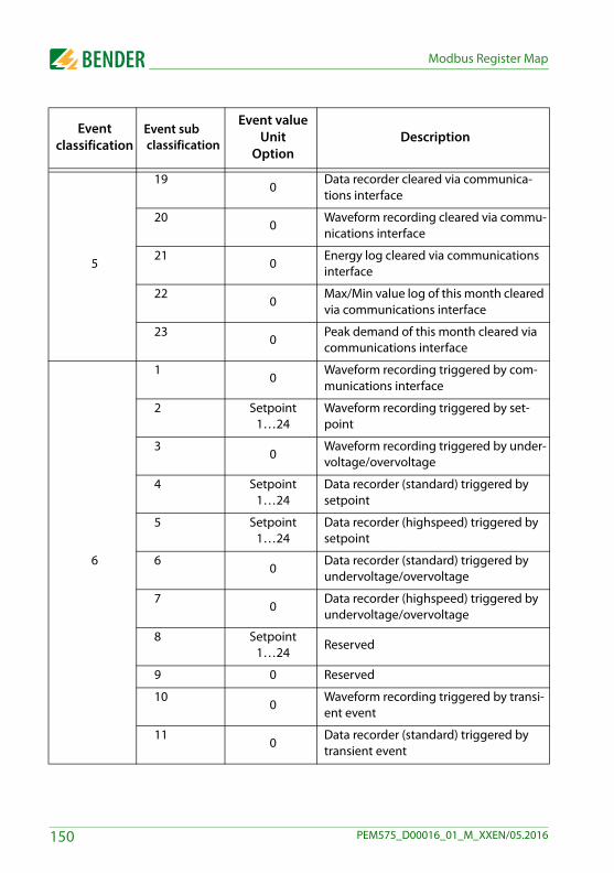
Modbus Register Map
5
190
Data recorder cleared via communica-tions interface
200
Waveform recording cleared via commu-nications interface
210
Energy log cleared via communications interface
220
Max/Min value log of this month cleared via communications interface
230
Peak demand of this month cleared via communications interface
6
10
Waveform recording triggered by com-munications interface
2 Setpoint 1…24
Waveform recording triggered by set-point
30
Waveform recording triggered by under-voltage/overvoltage
4 Setpoint 1…24
Data recorder (standard) triggered by setpoint
5 Setpoint 1…24
Data recorder (highspeed) triggered by setpoint
60
Data recorder (standard) triggered by undervoltage/overvoltage
70
Data recorder (highspeed) triggered by undervoltage/overvoltage
8 Setpoint 1…24
Reserved
9 0 Reserved
100
Waveform recording triggered by transi-ent event
110
Data recorder (standard) triggered by transient event
Event classification
Event sub classification
Event valueUnit
OptionDescription
150 PEM575_D00016_01_M_XXEN/05.2016
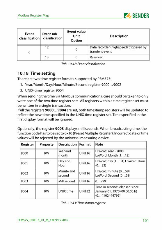
Modbus Register Map
Tab. 10.42: Event classification
10.18 Time settingThere are two time register formats supported by PEM575:
1. Year/Month/Day/Hour/Minute/Second register 9000…9002
2. UNIX-time register 9004
When sending the time via Modbus communications, care should be taken to only write one of the two time register sets. All registers within a time register set must be written in a single transaction.If all the registers 9000…9004 are set, both timestamp registers will be updated to reflect the new time specified in the UNIX time register set. Time specified in the first display format will be ignored.
Optionally, the register 9003 displays milliseconds. When broadcasting time, the function code has to be set to 0x10 (Preset Multiple Register). Incorrect date or time values will be rejected by the universal measuring device.
Tab. 10.43: Timestamp register
612
0Data recorder (highspeed) triggered by transient event
13 0 Reserved
Register Property Description Format Note
9000 RWYear and month
UINT16HiWord: Year - 2000LoWord: Month (1…12)
9001 RWDay and Hour
UINT16HiWord: day (1…31) LoWord: Hour (0…23)
9002 RWMinute andsecond
UINT16HiWord: minute (0…59) LoWord: Second (0…59)
9003 RW Millisecond UINT16 0…999
9004 RW UNIX time UINT32Time in seconds elapsed since January 01, 1970 (00:00:00 h) (0…4102444799)
Event classification
Event sub classification
Event valueUnit
OptionDescription
151PEM575_D00016_01_M_XXEN/05.2016
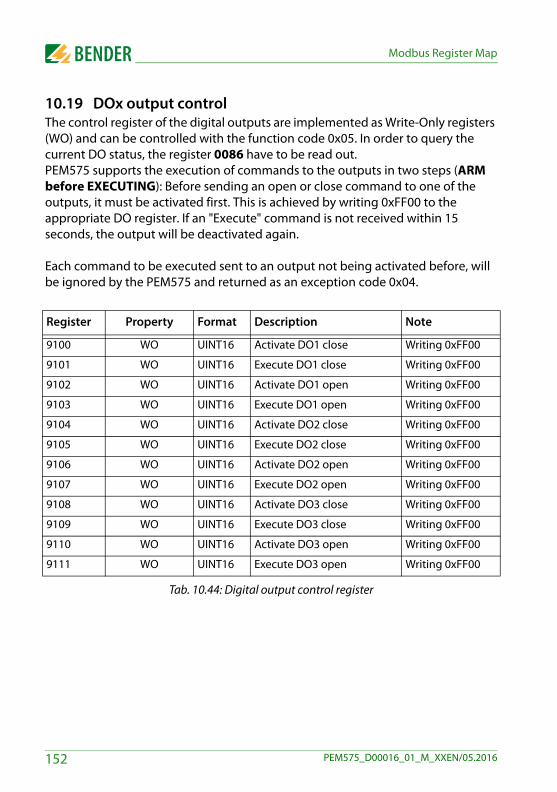
Modbus Register Map
10.19 DOx output controlThe control register of the digital outputs are implemented as Write-Only registers (WO) and can be controlled with the function code 0x05. In order to query the current DO status, the register 0086 have to be read out.PEM575 supports the execution of commands to the outputs in two steps (ARM before EXECUTING): Before sending an open or close command to one of the outputs, it must be activated first. This is achieved by writing 0xFF00 to the appropriate DO register. If an "Execute" command is not received within 15 seconds, the output will be deactivated again.
Each command to be executed sent to an output not being activated before, will be ignored by the PEM575 and returned as an exception code 0x04.
Tab. 10.44: Digital output control register
Register Property Format Description Note
9100 WO UINT16 Activate DO1 close Writing 0xFF00
9101 WO UINT16 Execute DO1 close Writing 0xFF00
9102 WO UINT16 Activate DO1 open Writing 0xFF00
9103 WO UINT16 Execute DO1 open Writing 0xFF00
9104 WO UINT16 Activate DO2 close Writing 0xFF00
9105 WO UINT16 Execute DO2 close Writing 0xFF00
9106 WO UINT16 Activate DO2 open Writing 0xFF00
9107 WO UINT16 Execute DO2 open Writing 0xFF00
9108 WO UINT16 Activate DO3 close Writing 0xFF00
9109 WO UINT16 Execute DO3 close Writing 0xFF00
9110 WO UINT16 Activate DO3 open Writing 0xFF00
9111 WO UINT16 Execute DO3 open Writing 0xFF00
152 PEM575_D00016_01_M_XXEN/05.2016
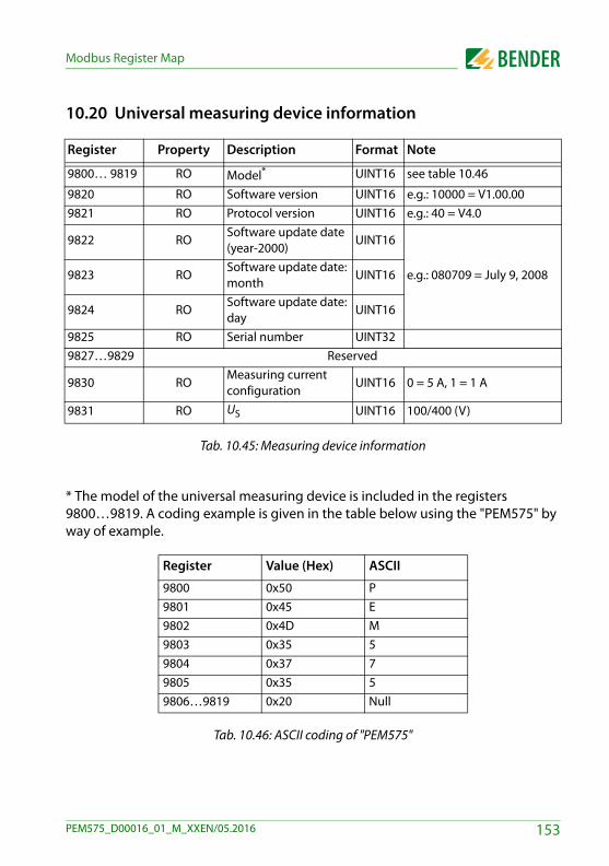
Modbus Register Map
10.20 Universal measuring device information
Tab. 10.45: Measuring device information
* The model of the universal measuring device is included in the registers 9800…9819. A coding example is given in the table below using the "PEM575" by way of example.
Tab. 10.46: ASCII coding of "PEM575"
Register Property Description Format Note
9800… 9819 RO Model* UINT16 see table 10.46
9820 RO Software version UINT16 e.g.: 10000 = V1.00.009821 RO Protocol version UINT16 e.g.: 40 = V4.0
9822 ROSoftware update date (year-2000)
UINT16
e.g.: 080709 = July 9, 20089823 ROSoftware update date: month
UINT16
9824 ROSoftware update date: day
UINT16
9825 RO Serial number UINT329827…9829 Reserved
9830 ROMeasuring current configuration
UINT16 0 = 5 A, 1 = 1 A
9831 RO US UINT16 100/400 (V)
Register Value (Hex) ASCII
9800 0x50 P9801 0x45 E9802 0x4D M9803 0x35 59804 0x37 79805 0x35 59806…9819 0x20 Null
153PEM575_D00016_01_M_XXEN/05.2016

Modbus Register Map
154 PEM575_D00016_01_M_XXEN/05.2016
11. Technical data
Insulation co-ordination
Measuring circuitRated insulation voltage ......................................................................................................................................................300 VOvervoltage category................................................................................................................................................................. IIIPollution degree.......................................................................................................................................................................... 2
Supply circuitRated insulation voltage ......................................................................................................................................................300 VOvervoltage category.................................................................................................................................................................. IIPollution degree.......................................................................................................................................................................... 2
Supply voltageRated supply voltage US ...............................................................................................................................AC/DC 95…415 VFrequency range of US ..................................................................................................................................... DC, 44…440 HzPower consumption ....................................................................................................................................................... ≤ 11 VA
Measuring circuit
Measuring voltage inputsUL1-N,L2-N,L3-N......................................................................................................................................................................230 V................................................................................................................................................................400 V (only -451, -455)..................................................................................................................................................................69 V (only -151, -155)UL1-L2,L2-L3,L3-L1 ..................................................................................................................................................................400 V................................................................................................................................................................690 V (only -451, -455)................................................................................................................................................................120 V (only -151, -155)Measuring range ...............................................................................................................................................10… 120 % UNRated frequency .........................................................................................................................................................45…65 HzInternal resistance (L-N)............................................................................................................................................... > 500 kΩ
Measuring current inputsExternal measuring current transformer....................................................... should at least comply with accuracy class 0,5 SBurden................................................................................................................................... n.A., internal current transformersMeasuring range ................................................................................................................................................ 0.1… 120% INPEM575/PEM575-455/PEM575-155
In .......................................................................................................................................................................5 AMeasuring current transformer ratio ...................................................................................................1…6000Accuracy class according with 5 A measuring current transformer .............................................................. 0,2
155PEM575_D00016_01_M_XXEN/05.2016
Technical data
Accuracy class according with 1 A measuring current transformer............................................................... 0,5PEM575-251/PEM575-451/PEM575-151
In ...................................................................................................................................................................... 1 AMeasuring current transformer ratio ................................................................................................. 1…30000Accuracy class according with 1 A measuring current transformer .............................................................. 0,2
Accuracies (v.M. = of measured value/v.S. = of full scale value)Phase voltage UL1-N, UL2-N, UL3-N .................................................................................................. ± 0.1 % of measured valueCurrent ............................................................................................................................................. ±0.1 % v.M./ +0.05% v.S.Neutral current I4 ........................................................................................................................................................ 0.5 % v. S.Frequency .....................................................................................................................................................................± 0.01 HzPhasing .................................................................................................................................................................................± 1 °Measurement of the active energy 0.2S ..........................................................acc. to DIN EN 62053-22 (VDE 0418 Part 3-22)Measurement of the voltage r.m.s. values .........................................acc. to DIN EN 61557-12 (VDE 0413-12), chapter 4.7.6Measurement of the phase current r.m.s. values ...............................acc. to DIN EN 61557-12 (VDE 0413-12), chapter 4.7.5Measurement of the frequency ..........................................................acc. to DIN EN 61557-12 (VDE 0413-12), chapter 4.7.4
InterfaceInterface / protocol .............................................................................................................................. RS-485 / Modbus RTUBaud rate ......................................................................................................................................................... 1.2…19.2 kBit/sCable length .............................................................................................................................................................0…1200 mRecommended cable (shielded, shield connected to SH on one side) ............................................. min. J-Y(St)Y min. 2x0.8Interface/protocol ............................................................................................................................. Ethernet, Modbus TCPBaud rate ...................................................................................................................................................................100 Mbits/s
Switching elementsOutputs ................................................................................................................................................................ 3 N/O contactsOperating principle .............................................................................................................................................. N/O operationRated operational voltage AC 230 V DC 24 V AC 110 V DC 12 VRated operational current 5 A 5 A 6 A 5 AMinimum contact rating ......................................................................................................................... 1 mA at AC/DC ≥ 10 VInputs ............................................................................................................................... 6 electrically separated digital inputsImin .....................................................................................................................................................................................2.4 mAUDI .....................................................................................................................................................................................DC 24 V
Environment / EMCEMC .......................................................................................................................................................................... IEC 61326-1Operating temperature........................................................................................................................................ –25…+55 °CClimatic class according to IEC 60721 (stationary use)........................................................................................................ 3K5Classification of mechanical conditions acc. to IEC 60721 (stationary use) ....................................................................... 3M4Height ...........................................................................................................................................................................to 4000 m
156 PEM575_D00016_01_M_XXEN/05.2016
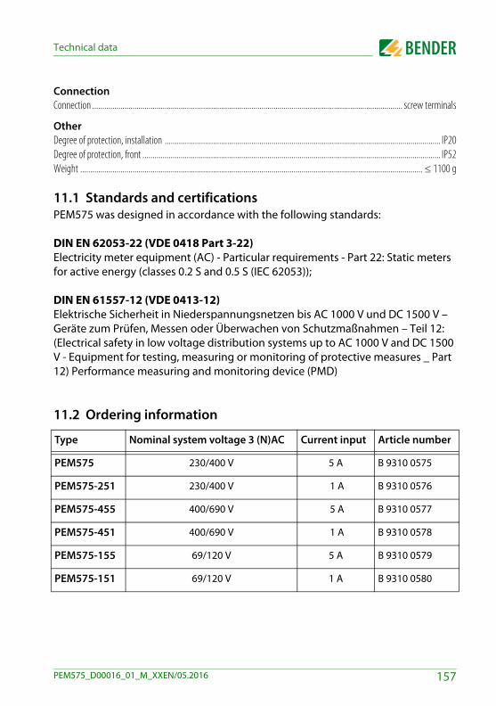
Technical data
Connection Connection .......................................................................................................................................................... screw terminals
OtherDegree of protection, installation ......................................................................................................................................... IP20Degree of protection, front .................................................................................................................................................... IP52Weight .......................................................................................................................................................................... ≤ 1100 g
11.1 Standards and certificationsPEM575 was designed in accordance with the following standards:
DIN EN 62053-22 (VDE 0418 Part 3-22) Electricity meter equipment (AC) - Particular requirements - Part 22: Static meters for active energy (classes 0.2 S and 0.5 S (IEC 62053));
DIN EN 61557-12 (VDE 0413-12) Elektrische Sicherheit in Niederspannungsnetzen bis AC 1000 V und DC 1500 V – Geräte zum Prüfen, Messen oder Überwachen von Schutzmaßnahmen – Teil 12: (Electrical safety in low voltage distribution systems up to AC 1000 V and DC 1500 V - Equipment for testing, measuring or monitoring of protective measures _ Part 12) Performance measuring and monitoring device (PMD)
11.2 Ordering information
Type Nominal system voltage 3 (N)AC Current input Article number
PEM575 230/400 V 5 A B 9310 0575
PEM575-251 230/400 V 1 A B 9310 0576
PEM575-455 400/690 V 5 A B 9310 0577
PEM575-451 400/690 V 1 A B 9310 0578
PEM575-155 69/120 V 5 A B 9310 0579
PEM575-151 69/120 V 1 A B 9310 0580
157PEM575_D00016_01_M_XXEN/05.2016

Technical data
158 PEM575_D00016_01_M_XXEN/05.2016
INDEX
AApparent power, calculation 47Application example 17Area of application 15
BBack-up fuses 21Button
- "ENERGY" 40- "HARMONICS" 29, 39- "POWER" 29- "V/I" 29, 35
CCalculation individual harmonic distortion 48Commissioning 27Configuration example
- 49Connection
- Three-phase 4-wire system 23Connection diagram
- Connection via voltage transformers 25- Three-phase 3-wire system 24- Three-phase 3-wire systems 25- Three-phase 4-wire system 23
Connection of measuring current transformers 21Connection via voltage transformers 25Control
- Digital outputs 152
DDemand 53Demand display 32Demand period 54
Description of function 17Device features 15Digital inputs 25, 51Digital output 26
- Modbus control 152Digital outputs 51Dimension diagram 19Display 30, 32Display mode
- Data display 34- Standard display 34
DOx control 152
EEnergy log 76Energy pulsing
- Display 52- enable/disable 45- LED indication 34
Event- Classification 141- Logging 79- Modbus register 139
FFront panel mounting 20Front view 18
HHarmonics 39, 81How to use this manual 9
IInputs, digital 25
159PEM575_D00016_01_M_XXEN/05.2016

INDEX
Installation 19Intended use 13
Kk-factor 39
LLC display
- Power and current demands 32- Standard display areas 30– 32- testing 30
LED indication 34Logging
- data recorder 62- Event 79- Max and Min values 61- Peak demand 61- Power Quality 78- Waveform recording 77
Logic modules 59
MMeasured quantities for data recorders 64measuring current transformers 21Modbus
- Basic measurements 87- Clear/reset 121- Energy measurement 91- Event log 139- High-speed measurement 97- Logic module 127- Max/Min log 108- Measuring device information 153- Peak demand 106- Power Quality (Fundamental) 93- Power Quality (Harmonics) 95- Register Map 85- Setpoint setup 123- Setup parameters 116
- SOE log 139- TCP (connector pin assignment) 26
OOperating elements 29Output, digital 26
PPhase angle
- Current 53- Voltage 53
Power factor rules 47Power Quality 81, 93Pulse counter 92
RRear view 18
SSafety instructions 14, 19, 21Service 10Set demand period 54Setpoint trigger 58Setup
- Setting options 43– 47Sliding Window 54SOE log
- Data structure 107- Modbus 139
Standard display areas 30Start
- Function of the buttons 41- Overview diagram menu 42- SETUP mode 41
Support 10
TTechnical data 155
160 PEM575_D00016_01_M_XXEN/05.2016
INDEX
TEHD 39, 81Testing LCD 30THD 39Time setting 151Time zones 121TOHD 39, 81Total harmonic distortion 39
UUnbalance 83
VVersions 16
WWiring diagram 22Work activities on electrical installations 13Workshops 11
161PEM575_D00016_01_M_XXEN/05.2016

INDEX
162 PEM575_D00016_01_M_XXEN/05.2016


Bender GmbH & Co. KGPostfach 1161 • 35301 Gruenberg • GermanyLondorfer Str. 65 • 35305 Gruenberg • Germany
Tel.: +49 6401 807-0Fax: +49 6401 807-259
E-Mail: [email protected]: Bender
Related Documents