exceet electronics GesmbH Wildbichler Straße 2e / A - 6341 Ebbs Tel: +43 5373 43143-0 Fax: +43 5373 43143-888 [email protected] www.exceet-electronics.at Doku-Nr.: PE3086, Version: 9 Design Guidelines For Manufacturing of Circuit Boards and Modules and for Layout Design

Welcome message from author
This document is posted to help you gain knowledge. Please leave a comment to let me know what you think about it! Share it to your friends and learn new things together.
Transcript
exceet electronics GesmbH
Wildbichler Straße 2e / A - 6341 Ebbs
Tel: +43 5373 43143-0
Fax: +43 5373 43143-888
www.exceet-electronics.at
Doku-Nr.: PE3086, Version: 9
Design Guidelines
For Manufacturing of Circuit Boards and Modules and for Layout Design
Design Guidelines exceet electronics Version 9
Page 2 of 15
Document: PE3086_Design-Guidelines_exceet-electronics.docx
Document No: PE3086
Version of template: 5
Table of Contents Table of Contents ........................................................................................................................................................................ 2
1 Preface .................................................................................................................................................................................. 3
1.1 Overview ..................................................................................................................................................................... 3
Circuit Board ................................................................................................................................................................ 3
Surface Mounted Technology ...................................................................................................................................... 3
Through Hole Technology ........................................................................................................................................... 3
2 Circuit Board ........................................................................................................................................................................ 4
2.1 Min/Max Circuit Boards and Panel Dimensions ........................................................................................................... 4
2.2 Panel Design ............................................................................................................................................................... 5
2.3 Base Material .............................................................................................................................................................. 5
2.4 Circuit Board Print ....................................................................................................................................................... 5
2.5 Layer Thickness of Circuit Board Surface .................................................................................................................... 5
2.6 Pad Surface................................................................................................................................................................. 6
2.7 Solder Resist Mask ...................................................................................................................................................... 6
2.8 Clear Space for Barcode Labels .................................................................................................................................. 6
2.9 Fiducials ...................................................................................................................................................................... 6
2.9.1 Circuit Board Fiducial ..................................................................................................................................... 6
2.9.2 X-out Fiducial ................................................................................................................................................. 7
2.9.3 Offset Fiducial ................................................................................................................................................ 7
2.9.4 Recommended Fiducial .................................................................................................................................. 7
2.10 Depaneling .................................................................................................................................................................. 7
2.11 Dataset ........................................................................................................................................................................ 8
3 SMT ....................................................................................................................................................................................... 9
3.1 Component packaging ................................................................................................................................................. 9
3.2 Pad Geometry ............................................................................................................................................................. 9
3.3 Note on BGA's ............................................................................................................................................................. 9
3.4 Assembling Data ....................................................................................................................................................... 10
3.4.1 Example ....................................................................................................................................................... 10
3.5 SMT Soldering ........................................................................................................................................................... 10
3.5.1 Double-sided ................................................................................................................................................ 10
3.5.2 Soldering Profile Vapor Phase ...................................................................................................................... 11
3.5.3 Soldering Profile Reflow ............................................................................................................................... 11
4 THT...................................................................................................................................................................................... 12
4.1 Component Arrangement .......................................................................................................................................... 12
4.1.1 Selective Wave Soldering ............................................................................................................................. 12
4.2 Soldering Profile Wave .............................................................................................................................................. 12
5 Design for Testability ......................................................................................................................................................... 13
5.1 Constructive Designrules ........................................................................................................................................... 13
5.1.1 Contacting .................................................................................................................................................... 13
5.1.2 Center Holes ................................................................................................................................................ 13
5.1.3 Test Points ................................................................................................................................................... 13
5.2 Electrical Designrules ................................................................................................................................................ 13
5.2.1 Functional tests with high current loads ........................................................................................................ 13
5.2.2 Arrays / Serial connections of resistors ......................................................................................................... 13
5.2.3 4-wire measuring .......................................................................................................................................... 13
6 Coatability of a PCB ........................................................................................................................................................... 14
7 References ......................................................................................................................................................................... 14
8 Contact Person .................................................................................................................................................................. 14
9 Disclaimer ........................................................................................................................................................................... 15

Design Guidelines exceet electronics Version 9
Page 3 of 15
Document: PE3086_Design-Guidelines_exceet-electronics.docx
Document No: PE3086
Version of template: 5
1 Preface This document contains the design guidelines respectively the requirements for manufacturing high-quality printed circuit boards at exceet electronics. If there are for some reasons deviations, the detailed technical conditions have to be discussed.
1.1 Overview
Circuit Board
This section describes all preconditions relevant for production-oriented circuit boards like dimensions, tolerances, properties, fiducials, surface, panel design etc.
Surface Mounted Technology
In this section some design rules for designing SMT layouts (pad geometries, component gaps etc.) have been summarized. Another topic is the optimal data format and the production-oriented component packing.
Through Hole Technology
This section describes the proper positioning of THT components in order to achieve an optimal wave soldering result. Further some recommendations regarding component gaps for mixed assemblies are given.
Design Guidelines exceet electronics Version 9
Page 4 of 15
Document: PE3086_Design-Guidelines_exceet-electronics.docx
Document No: PE3086
Version of template: 5
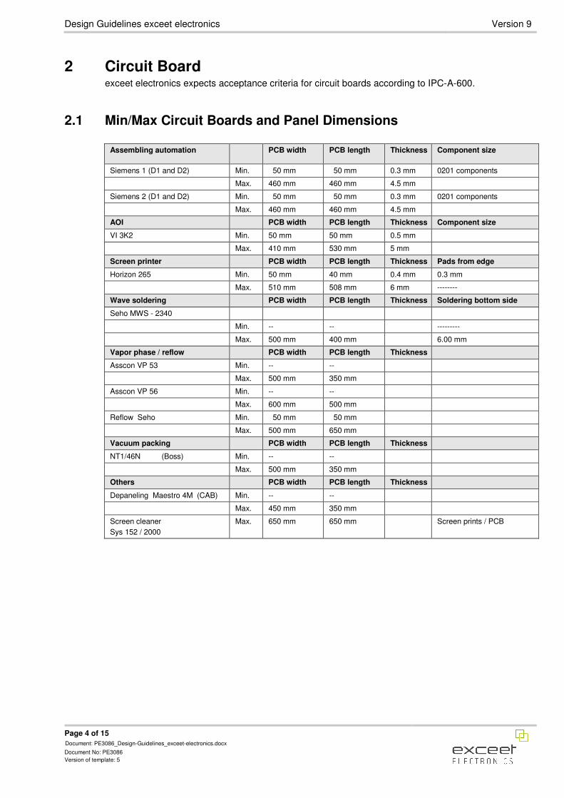
2 Circuit Board exceet electronics expects acceptance criteria for circuit boards according to IPC-A-600.
2.1 Min/Max Circuit Boards and Panel Dimensions
Assembling automation PCB width PCB length Thickness Component size
Siemens 1 (D1 and D2) Min. 50 mm 50 mm 0.3 mm 0201 components
Max. 460 mm 460 mm 4.5 mm
Siemens 2 (D1 and D2) Min. 50 mm 50 mm 0.3 mm 0201 components
Max. 460 mm 460 mm 4.5 mm
AOI PCB width PCB length Thickness Component size
VI 3K2 Min. 50 mm 50 mm 0.5 mm
Max. 410 mm 530 mm 5 mm
Screen printer PCB width PCB length Thickness Pads from edge
Horizon 265 Min. 50 mm 40 mm 0.4 mm 0.3 mm
Max. 510 mm 508 mm 6 mm --------
Wave soldering PCB width PCB length Thickness Soldering bottom side
Seho MWS - 2340
Min. -- -- ---------
Max. 500 mm 400 mm 6.00 mm
Vapor phase / reflow PCB width PCB length Thickness
Asscon VP 53 Min. -- --
Max. 500 mm 350 mm
Asscon VP 56 Min. -- --
Max. 600 mm 500 mm
Reflow Seho Min. 50 mm 50 mm
Max. 500 mm 650 mm
Vacuum packing PCB width PCB length Thickness
NT1/46N (Boss) Min. -- --
Max. 500 mm 350 mm
Others PCB width PCB length Thickness
Depaneling Maestro 4M (CAB) Min. -- --
Max. 450 mm 350 mm
Screen cleaner
Sys 152 / 2000
Max. 650 mm 650 mm Screen prints / PCB

Design Guidelines exceet electronics Version 9
Page 5 of 15
Document: PE3086_Design-Guidelines_exceet-electronics.docx
Document No: PE3086
Version of template: 5
2.2 Panel Design For transporting and clamping of the PCB, the SMT components shall have a distance to the edge of at least 5 mm.
If the required 5 mm cannot be kept, then consultation with the NPI or CAD department of exceet electronics is required. Maybe a special panel design or an additional edge has to be provided.
2.3 Base Material FR4 (Standard at exceet electronics)
If other base materials should be used / required, please consult the CAD department of exceet electronics.
2.4 Circuit Board Print The print width and the gap to the pads is at least 0.2 mm. Pads must not be overprinted.
Different colors (on demand) can be realized - standard is white.
2.5 Layer Thickness of Circuit Board Surface Layer thickness of circuit board surface has to ensure sufficient wetting during repeated soldering.
The following layer thicknesses are required:
• Immersion tin (Sn) ≥1.0 µ
• Immersion silver (Ag) ≥0,15u
• Immersion nickel-gold (Ni-Au) 3u bis 6u / 0,05u bis 0,12u
• Hot Air Leveling (HAL) (lead-free) ≥1u ≤25u
• Electrolytic gold typical 1,0u

Design Guidelines exceet electronics Version 9
Page 6 of 15
Document: PE3086_Design-Guidelines_exceet-electronics.docx
Document No: PE3086
Version of template: 5
2.6 Pad Surface With respect to cost effectiveness and customer preference, the following procedure are preferred to obtain a solderable surface.
• Immersion tin (Sn) (on customer preference)
• Immersion silver (Ag) (on customer preference)
• Immersion nickel-gold (Ni-Au) (Standard at exceet electronics)
• Hot Air Leveling (HAL) (lead-free) (after consultation)
• Organic Cu solderability preservative (OSP) (after consultation)
2.7 Solder Resist Mask Since the manufacturer of the circuit boards adapts the board himself, the cuts should have the same data as the pads.
If possible, solder resist should be also provided between the fine pitch pads.
To prevent short-curcuits, vias should be covered with solder resist (only onesided) unless they are used as test positions.
2.8 Clear Space for Barcode Labels If possible, a clear space of 8 x 8 mm for 2D barcode labels should be provided on the circuit board.
2.9 Fiducials Basically there are two different kinds of fiducials on the circuit board.
2.9.1 Circuit Board Fiducial
In order to have a reference point on the circuit board, at least two fiducials should be on the board, preferably in diagonal direction and with maximum distance. Fiducials should be placed on Top-Side and BOT-Side. (Even at onesided designs)
The best would be to use differents shapes for the two fiducials. This is especially important when using symmetric assemblies.
Minimum distance of fiducial to circuit board edge
X direction Y direction
5 mm 5 mm
For boards in panels the panel should provide at least two additional fiducials. For positioning these marks the same guidelines as for the circuit boards should be applied.
Design Guidelines exceet electronics Version 9
Page 7 of 15
Document: PE3086_Design-Guidelines_exceet-electronics.docx
Document No: PE3086
Version of template: 5
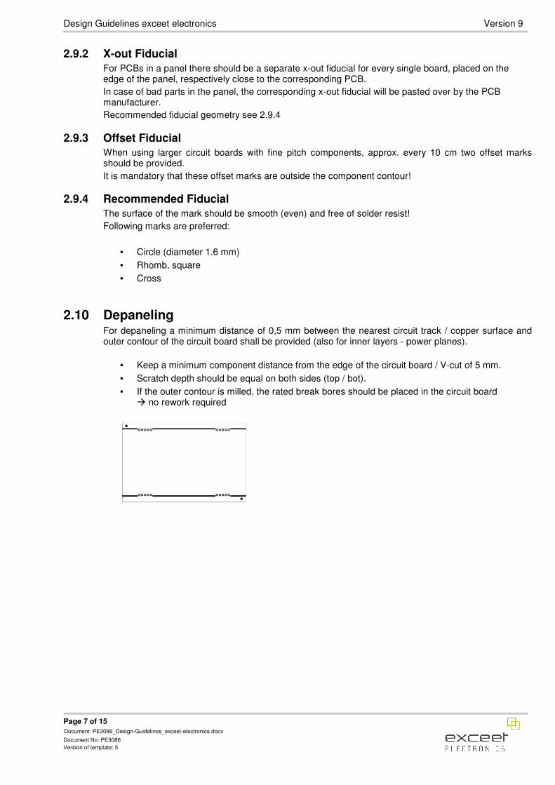
2.9.2 X-out Fiducial
For PCBs in a panel there should be a separate x-out fiducial for every single board, placed on the edge of the panel, respectively close to the corresponding PCB.
In case of bad parts in the panel, the corresponding x-out fiducial will be pasted over by the PCB manufacturer.
Recommended fiducial geometry see 2.9.4
2.9.3 Offset Fiducial
When using larger circuit boards with fine pitch components, approx. every 10 cm two offset marks should be provided.
It is mandatory that these offset marks are outside the component contour!
2.9.4 Recommended Fiducial
The surface of the mark should be smooth (even) and free of solder resist!
Following marks are preferred:
• Circle (diameter 1.6 mm)
• Rhomb, square
• Cross
2.10 Depaneling For depaneling a minimum distance of 0,5 mm between the nearest circuit track / copper surface and outer contour of the circuit board shall be provided (also for inner layers - power planes).
• Keep a minimum component distance from the edge of the circuit board / V-cut of 5 mm.
• Scratch depth should be equal on both sides (top / bot).
• If the outer contour is milled, the rated break bores should be placed in the circuit board no rework required
Design Guidelines exceet electronics Version 9
Page 8 of 15
Document: PE3086_Design-Guidelines_exceet-electronics.docx
Document No: PE3086
Version of template: 5
2.11 Dataset The circuit board data should contain the following information:
• Layer data in Extended Gerber Format
• Readme file with notes on:
- Base material
- Circuit board thickness
- Copper thickness
- Surface
- Colour of solder mask
- Assembly print *
- Layer design / key to Gerber data names
- Special remarks
• Drill data in Excellon format (seperate file for NPTH and PTH)
• Layer for Pastemask
• Design file for optical check and InCurcuit-Test (ODB++, Cadif, for Eagle Designs brd file or Fabmaster)
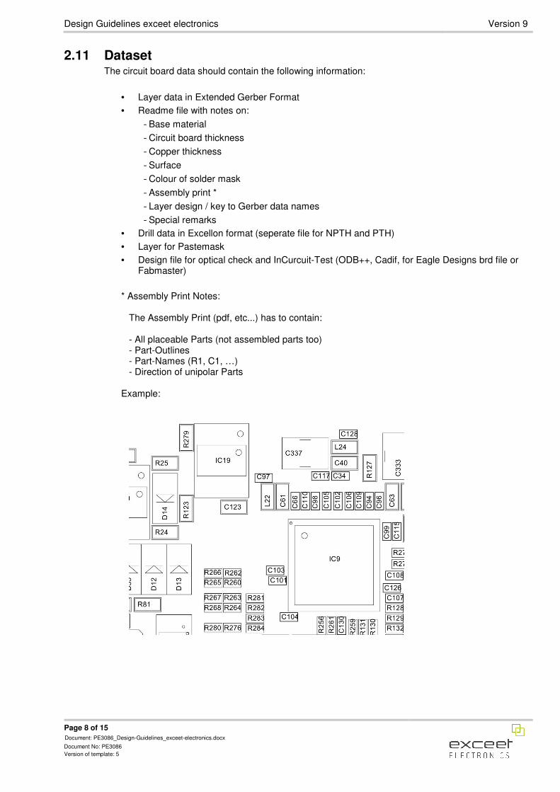
* Assembly Print Notes: The Assembly Print (pdf, etc...) has to contain: - All placeable Parts (not assembled parts too) - Part-Outlines - Part-Names (R1, C1, …) - Direction of unipolar Parts Example:
Design Guidelines exceet electronics Version 9
Page 9 of 15
Document: PE3086_Design-Guidelines_exceet-electronics.docx
Document No: PE3086
Version of template: 5
3 SMT
3.1 Component packaging • Strip (reel) (preferred)
• Tray (wafer) (preferred)
• Tube (stick) (only for small batches)
The components should be capable for automated assembling. If special shapes or plugs are used, the components should be available with pick & place pads. If not, please contact the NPI department at exceet electronics; maybe pick tests can be made or special tools can be designed.
3.2 Pad Geometry Basically, for each component there's a land pattern which represents the manufacturer's recommendation for the pad geometry.
Optimal pad geometries are described in detail in the IPC standard. To achieve the optimal geometry, a Land Pattern Generator can be used:
http://www.pcblibraries.com/
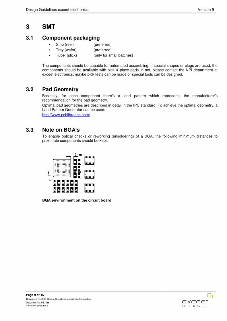
3.3 Note on BGA's To enable optical checks or reworking (unsoldering) of a BGA, the following minimum distances to proximate components should be kept:
BGA environment on the circuit board
Design Guidelines exceet electronics Version 9
Page 10 of 15
Document: PE3086_Design-Guidelines_exceet-electronics.docx
Document No: PE3086
Version of template: 5
3.4 Assembling Data Attention: coordinate data for SMT assembling should contain following information.
• Assembly position of all placeable parts (not assembled parts too)
• Component identification / design
• X coordinates from center of component (unit = mm)
• Y coordinates from center of component (unit = mm)
• Rotation
The position of the fiducials should be integrated in the coordinate file also.
The origin of assembly data (xy) should be the lower left edge of the PCB.
Data have to be separated by a distinct separator mark.
3.4.1 Example
D5|0805LED_KPT2012MGC|38.418|29.210|270.0
D6|0805LED_KPT2012MGC|38.418|24.130|270.0
D7|0805LED_KPT2012SYC|59.055|66.358|90.0
F1|EIA481-2_SMD2920P075TS|43.180|26.670|270.0
IC1|TQFP44_T89C51CC01UA|35.560|56.515|0.0
IC2|SO08_82C251T|45.085|5.080|180.0
IC3|NB|31.750|26.670|0.0
FID1|Fiducial_1|10.000|5.000|0.0
FID2| Fiducial_2|150.000|95.000|0.0
3.5 SMT Soldering
3.5.1 Double-sided
In order to avoid that components detach from the circuit board during the second soldering process, following notes should be observed:
• The circuit board and the components should endure the additional temperature stress without defects.
• The components should be arranged on the circuit board such that all light-weight parts are on one side and all heavy parts on the other side. This is a precondition that no component detaches from the board during the second soldering process.
Design Guidelines exceet electronics Version 9
Page 11 of 15
Document: PE3086_Design-Guidelines_exceet-electronics.docx
Document No: PE3086
Version of template: 5
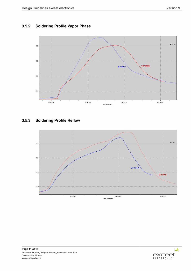
3.5.2 Soldering Profile Vapor Phase
3.5.3 Soldering Profile Reflow
Design Guidelines exceet electronics Version 9
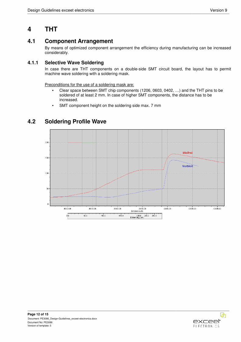
Page 12 of 15
Document: PE3086_Design-Guidelines_exceet-electronics.docx
Document No: PE3086
Version of template: 5
4 THT
4.1 Component Arrangement By means of optimized component arrangement the efficiency during manufacturing can be increased considerably.
4.1.1 Selective Wave Soldering
In case there are THT components on a double-side SMT circuit board, the layout has to permit machine wave soldering with a soldering mask.
Preconditions for the use of a soldering mask are:
• Clear space between SMT chip components (1206, 0603, 0402, …) and the THT pins to be soldered of at least 2 mm. In case of higher SMT components, the distance has to be increased.
• SMT component height on the soldering side max. 7 mm
4.2 Soldering Profile Wave
Design Guidelines exceet electronics Version 9
Page 13 of 15
Document: PE3086_Design-Guidelines_exceet-electronics.docx
Document No: PE3086
Version of template: 5
5 Design for Testability The design of the board has an significant impact on the achievable quality of testing.
5.1 Constructive Designrules
5.1.1 Contacting
To permit an InCurcuit-Test, all electrical nets of the board have to be contacted. It is possible to contact on THT-pins, test pads and vias (lowest priority). Contacting on only one side of the board (top/bot) keeps the adapter price low.
5.1.2 Center Holes
To center the board in the test adapter, the design should contain additional (same drill-process than the other holes on the board) center holes. The diameter should be in the range of 2.00m – 3.5mm. To avoid an wrong insertion of the board, the center holes should be placed asymmetrical.
5.1.3 Test Points
Priority 1: 100mil Contact-Needle (default)
• Required diamter of test pads: >0.8mm
• Required distance from test pad to test pad (center <-> center): >2.05mm
Priority 2: 75mil Contact-Needle
• Required diamter of test pads: >0.4mm (preferred >0.5mm)
• Required distance from test pad to test pad (center <-> center): >1.65mm
Priority 3: 50mil Contact-Needle
• Required diamter of test pads: >0.2mm
• Required distance from test pad to test pad (center <-> center): >1.25mm
5.2 Electrical Designrules
5.2.1 Functional tests with high current loads
For currents above 0.5A, provide more than one contact points (test pads, THT-pins, vias)
5.2.2 Arrays / Serial connections of resistors
To measure resistance-arrays make sure that at least 1 of the internal resistors is contactable. To measure resistors that are connected in series it’s sufficient to provide contact points at both ends of the serial connection.
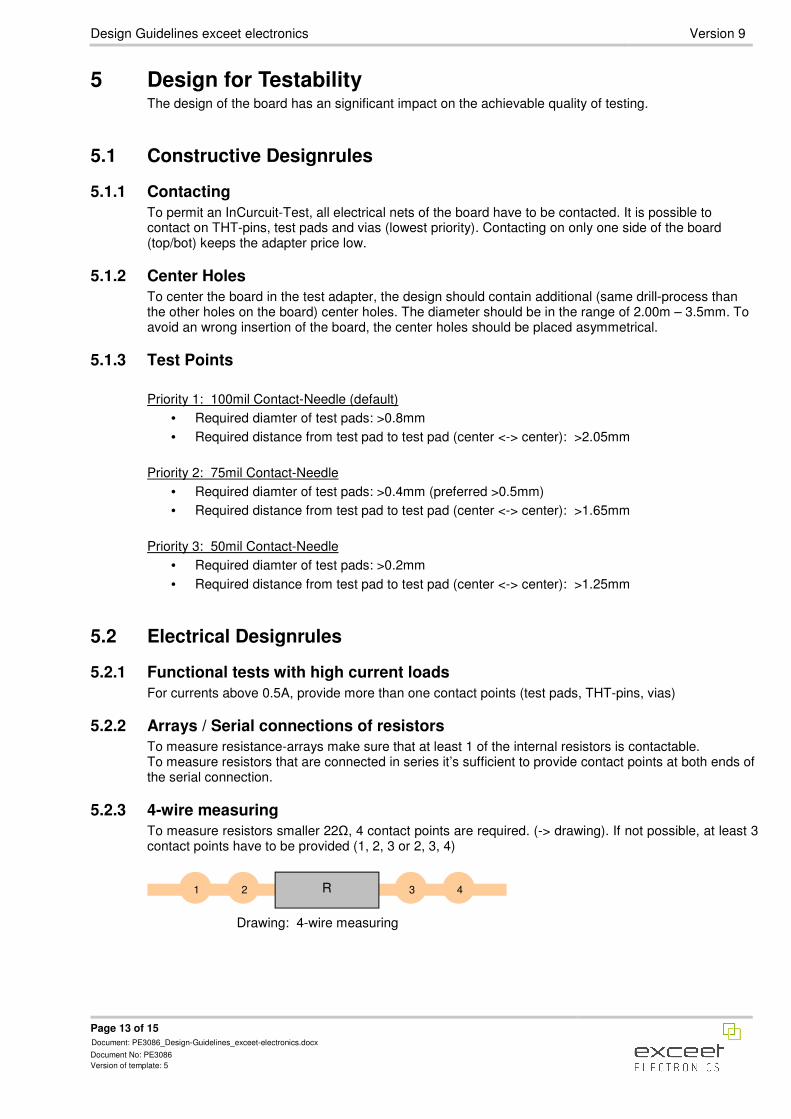
5.2.3 4-wire measuring
To measure resistors smaller 22Ω, 4 contact points are required. (-> drawing). If not possible, at least 3 contact points have to be provided (1, 2, 3 or 2, 3, 4)
Drawing: 4-wire measuring
1 4 3 2 R
Design Guidelines exceet electronics Version 9
Page 14 of 15
Document: PE3086_Design-Guidelines_exceet-electronics.docx
Document No: PE3086
Version of template: 5
6 Coatability of a PCB The layout has to be suitable for all common coating methods (dipping, flooding, spraying, etc.). Components that have not to be coated (plugs, sockets, switches, buzzer, dip switches, LEDs, etc.) must be maskable.
Precondition: The clearance around components that are not allowed to be coated should be >2mm.
7 References Acceptance criteria for electronic assemblies - IPC-A-610
8 Contact Person
Ing. Andreas Treichl
Leitung QM, NPI / quality and NPI manager
mail: [email protected]
tel: +43/5373/43143-611
__________________________________
Ing. Christoph Rieser
New Product Introduction
mail: [email protected]
tel: +43/5373/43143-651
__________________________________
Dipl.Ing.(FH) Wolf Dietrich Metz
Entwicklung Layout / PCB Design
mail: [email protected]
tel: +43/5373/43143-542
__________________________________
Ing. Günther Unterrainer
Entwicklung Layout / PCB Design
mail: [email protected]
tel: +43/5373/43143-541
__________________________________
Reinhard Osterauer
Prozesstechnik / process engineer
mail: [email protected]
tel: +43/5373/43143-722

Design Guidelines exceet electronics Version 9
Page 15 of 15
Document: PE3086_Design-Guidelines_exceet-electronics.docx
Document No: PE3086
Version of template: 5
9 Disclaimer
The processes and suggestions for use described in this document do not in any way constitute a guarantee.
The issuer accepts no liability for the accuracy and completeness of this document and its utilization.
Exceet electronics reserves the right to make technical changes to the document at any time without liability to inform the user thereof.
The use of the know-how in this document does not imply a liability of the issuer for claims of any kind.
This document may not be duplicated either in whole or in part, disseminated to third parties or utilized for another's own documentation.
This document is the intellectual property of the issuer.
Related Documents