TMS320C6701 FLOATINGĆPOINT DIGITAL SIGNAL PROCESSOR SPRS067F - MAY 1998 - REVISED MARCH 2004 1 POST OFFICE BOX 1443 • HOUSTON, TEXAS 77251-1443 D Highest Performance Floating-Point Digital Signal Processor (DSP) TMS320C6701 - 8.3-, 6.7-, 6-ns Instruction Cycle Time - 120-, 150-, 167-MHz Clock Rate - Eight 32-Bit Instructions/Cycle - 1 GFLOPS - TMS320C6201 Fixed-Point DSP Pin-Compatible D VelociTI Advanced Very Long Instruction Word (VLIW) C67x CPU Core - Eight Highly Independent Functional Units: - Four ALUs (Floating- and Fixed-Point) - Two ALUs (Fixed-Point) - Two Multipliers (Floating- and Fixed-Point) - Load-Store Architecture With 32 32-Bit General-Purpose Registers - Instruction Packing Reduces Code Size - All Instructions Conditional D Instruction Set Features - Hardware Support for IEEE Single-Precision Instructions - Hardware Support for IEEE Double-Precision Instructions - Byte-Addressable (8-, 16-, 32-Bit Data) - 8-Bit Overflow Protection - Saturation - Bit-Field Extract, Set, Clear - Bit-Counting - Normalization D 1M-Bit On-Chip SRAM - 512K-Bit Internal Program/Cache (16K 32-Bit Instructions) - 512K-Bit Dual-Access Internal Data (64K Bytes) D 32-Bit External Memory Interface (EMIF) - Glueless Interface to Synchronous Memories: SDRAM and SBSRAM - Glueless Interface to Asynchronous Memories: SRAM and EPROM - 52M-Byte Addressable External Memory Space D Four-Channel Bootloading Direct-Memory-Access (DMA) Controller With an Auxiliary Channel D 16-Bit Host-Port Interface (HPI) - Access to Entire Memory Map D Two Multichannel Buffered Serial Ports (McBSPs) - Direct Interface to T1/E1, MVIP, SCSA Framers - ST-Bus-Switching Compatible - Up to 256 Channels Each - AC97-Compatible - Serial-Peripheral-Interface (SPI) Compatible (Motorola) D Two 32-Bit General-Purpose Timers D Flexible Phase-Locked-Loop (PLL) Clock Generator D IEEE-1149.1 (JTAG † ) Boundary-Scan-Compatible D 352-Pin Ball Grid Array (BGA) Package (GJC Suffix) D 0.18-µm/5-Level Metal Process - CMOS Technology D 3.3-V I/Os, 1.8-V Internal (120-, 150-MHz) D 3.3-V I/Os, 1.9-V Internal (167-MHz Only) Copyright 2004, Texas Instruments Incorporated PRODUCTION DATA information is current as of publication date. Products conform to specifications per the terms of Texas Instruments standard warranty. Production processing does not necessarily include testing of all parameters. Please be aware that an important notice concerning availability, standard warranty, and use in critical applications of Texas Instruments semiconductor products and disclaimers thereto appears at the end of this data sheet. A B C D E F G H J K L M N P R T U V W Y AA AB AC AD AE AF 1 26 GJC (352-PIN BGA) PACKAGE ( BOTTOM VIEW ) VelociTI is a trademark of Texas Instruments. Motorola is a trademark of Motorola, Inc. † IEEE Standard 1149.1-1990 Standard-Test-Access Port and Boundary Scan Architecture.

Welcome message from author
This document is posted to help you gain knowledge. Please leave a comment to let me know what you think about it! Share it to your friends and learn new things together.
Transcript

SPRS067F − MAY 1998 − REVISED MARCH 2004
1POST OFFICE BOX 1443 • HOUSTON, TEXAS 77251−1443
Highest Performance Floating-Point DigitalSignal Processor (DSP) TMS320C6701− 8.3-, 6.7-, 6-ns Instruction Cycle Time− 120-, 150-, 167-MHz Clock Rate− Eight 32-Bit Instructions/Cycle− 1 GFLOPS− TMS320C6201 Fixed-Point DSP
Pin-Compatible
VelociTI Advanced Very Long InstructionWord (VLIW) C67x CPU Core− Eight Highly Independent Functional
Units:− Four ALUs (Floating- and Fixed-Point)− Two ALUs (Fixed-Point)− Two Multipliers (Floating- and
Fixed-Point)− Load-Store Architecture With 32 32-Bit
General-Purpose Registers− Instruction Packing Reduces Code Size− All Instructions Conditional
Instruction Set Features− Hardware Support for IEEE
Single-Precision Instructions− Hardware Support for IEEE
Double-Precision Instructions− Byte-Addressable (8-, 16-, 32-Bit Data)− 8-Bit Overflow Protection− Saturation− Bit-Field Extract, Set, Clear− Bit-Counting− Normalization
1M-Bit On-Chip SRAM− 512K-Bit Internal Program/Cache
(16K 32-Bit Instructions)− 512K-Bit Dual-Access Internal Data
(64K Bytes)
32-Bit External Memory Interface (EMIF)− Glueless Interface to Synchronous
Memories: SDRAM and SBSRAM− Glueless Interface to Asynchronous
Memories: SRAM and EPROM− 52M-Byte Addressable External Memory
Space
Four-Channel BootloadingDirect-Memory-Access (DMA) ControllerWith an Auxiliary Channel
16-Bit Host-Port Interface (HPI)− Access to Entire Memory Map
Two Multichannel Buffered Serial Ports(McBSPs)− Direct Interface to T1/E1, MVIP, SCSA
Framers− ST-Bus-Switching Compatible− Up to 256 Channels Each− AC97-Compatible− Serial-Peripheral-Interface (SPI)
Compatible (Motorola )
Two 32-Bit General-Purpose Timers
Flexible Phase-Locked-Loop (PLL) ClockGenerator
IEEE-1149.1 (JTAG†)Boundary-Scan-Compatible
352-Pin Ball Grid Array (BGA) Package(GJC Suffix)
0.18-µm/5-Level Metal Process− CMOS Technology
3.3-V I/Os, 1.8-V Internal (120-, 150-MHz)
3.3-V I/Os, 1.9-V Internal (167-MHz Only)
Copyright 2004, Texas Instruments Incorporated ! "#$ ! %#&'" ($)(#"! " !%$""! %$ *$ $! $+! !#$!!(( ,-) (#" %"$!!. ($! $"$!!'- "'#($$!. '' %$$!)
Please be aware that an important notice concerning availability, standard warranty, and use in critical applications ofTexas Instruments semiconductor products and disclaimers thereto appears at the end of this data sheet.
ABCDEFGHJKLMNPRTUVWYAAABACADAEAF
126
GJC (352-PIN BGA) PACKAGE(BOTTOM VIEW)
VelociTI is a trademark of Texas Instruments.Motorola is a trademark of Motorola, Inc.† IEEE Standard 1149.1-1990 Standard-Test-Access Port and Boundary Scan Architecture.

SPRS067F − MAY 1998 − REVISED MARCH 2004
2 POST OFFICE BOX 1443 • HOUSTON, TEXAS 77251−1443
Table of Contents
parameter measurement information 31. . . . . . . . . . . . . . .
signal-transition levels 31. . . . . . . . . . . . . . . . . . . . . . . . . . . .
input and output clocks 32. . . . . . . . . . . . . . . . . . . . . . . . . . .
asynchronous memory timing 35. . . . . . . . . . . . . . . . . . . . .
synchronous-burst memory timing 37. . . . . . . . . . . . . . . . .
synchronous DRAM timing 41. . . . . . . . . . . . . . . . . . . . . . . .
HOLD/HOLDA timing 45. . . . . . . . . . . . . . . . . . . . . . . . . . . .
reset timing 46. . . . . . . . . . . . . . . . . . . . . . . . . . . . . . . . . . . . .
external interrupt timing 48. . . . . . . . . . . . . . . . . . . . . . . . . .
host-port interface timing 49. . . . . . . . . . . . . . . . . . . . . . . . .
multichannel buffered serial port timing 52. . . . . . . . . . . . .
DMAC, timer, power-down timing 63. . . . . . . . . . . . . . . . . .
JTAG test-port timing 65. . . . . . . . . . . . . . . . . . . . . . . . . . . .
mechanical data 66. . . . . . . . . . . . . . . . . . . . . . . . . . . . . . . . . revision history 67. . . . . . . . . . . . . . . . . . . . . . . . . . . . . . . . . .
GJC BGA package (bottom view) 1. . . . . . . . . . . . . . . . . . . . . .
description 2. . . . . . . . . . . . . . . . . . . . . . . . . . . . . . . . . . . . . . . . .
device characteristics 3. . . . . . . . . . . . . . . . . . . . . . . . . . . . . . . .
functional block and CPU diagram 4. . . . . . . . . . . . . . . . . . . . .
CPU description 5. . . . . . . . . . . . . . . . . . . . . . . . . . . . . . . . . . . . .
signal groups description 7. . . . . . . . . . . . . . . . . . . . . . . . . . . . .
signal descriptions 9. . . . . . . . . . . . . . . . . . . . . . . . . . . . . . . . . . .
development support 20. . . . . . . . . . . . . . . . . . . . . . . . . . . . . . . .
documentation support 23. . . . . . . . . . . . . . . . . . . . . . . . . . . . . .
clock PLL 24. . . . . . . . . . . . . . . . . . . . . . . . . . . . . . . . . . . . . . . . . power-down logic mode 26. . . . . . . . . . . . . . . . . . . . . . . . . . . . .
absolute maximum ratings over operating casetemperature range 29. . . . . . . . . . . . . . . . . . . . . . . . . . . . .
recommended operating conditions 29. . . . . . . . . . . . . . . . . . .
electrical characteristics over recommended ranges ofsupply voltage and operating case temperature 30. . . .
description
The TMS320C67x DSPs are the floating-point DSP family in the TMS320C6000 DSP platform. TheTMS320C6701 (C6701) device is based on the high-performance, advanced VelociTIvery-long-instruction-word (VLIW) architecture developed by Texas Instruments (TI), making this DSP anexcellent choice for multichannel and multifunction applications. With performance of up to 1 giga floating-pointoperations per second (GFLOPS) at a clock rate of 167 MHz, the C6701 offers cost-effective solutions tohigh-performance DSP programming challenges. The C6701 DSP possesses the operational flexibility ofhigh-speed controllers and the numerical capability of array processors. This processor has 32 general-purposeregisters of 32-bit word length and eight highly independent functional units. The eight functional units providefour floating-/fixed-point ALUs, two fixed-point ALUs, and two floating-/fixed-point multipliers. The C6701 canproduce two multiply-accumulates (MACs) per cycle for a total of 334 million MACs per second (MMACS). TheC6701 DSP also has application-specific hardware logic, on-chip memory, and additional on-chip peripherals.
The C6701 includes a large bank of on-chip memory and has a powerful and diverse set of peripherals. Programmemory consists of a 64K-byte block that is user-configurable as cache or memory-mapped program space.Data memory consists of two 32K-byte blocks of RAM. The peripheral set includes two multichannel bufferedserial ports (McBSPs), two general-purpose timers, a host-port interface (HPI), and a glueless external memoryinterface (EMIF) capable of interfacing to SDRAM or SBSRAM and asynchronous peripherals.
The C6701 has a complete set of development tools which includes: a new C compiler, an assembly optimizerto simplify programming and scheduling, and a Windows debugger interface for visibility into source codeexecution.
TMS320C6000 is a trademark of Texas Instruments.Windows is a registered trademark of Microsoft Corporation.

SPRS067F − MAY 1998 − REVISED MARCH 2004
3POST OFFICE BOX 1443 • HOUSTON, TEXAS 77251−1443
device characteristics
Table 1 provides an overview of the C6701 DSP. The table shows significant features of each device, includingthe capacity of on-chip RAM, the peripherals, the execution time, and the package type with pin count, etc.
Table 1. Characteristics of the C6701 Processors
HARDWARE FEATURES C6701
EMIF 1
DMA 4-Channel
Peripherals Host-Port Interface (HPI) 1Peripherals
McBSPs 2
32-Bit Timers 2
Internal Program MemorySize (Bytes) 64K
Internal Program MemoryOrganization 64K Bytes Cache/Mapped Program
Internal Data MemorySize (Bytes) 64K
Internal Data MemoryOrganization 2 Blocks: Eight 16-Bit Banks per Block 50/50 Split
Frequency MHz 120, 150, 167
Cycle Time ns 6 ns (6701-167); 6.7 ns (6701-150); 8.3 ns (6701-120)
Core (V)1.8 (6701-120, -150)
VoltageCore (V)
1.9 (6701-167 only)Voltage
I/O (V) 3.3
PLL Options CLKIN frequency multiplier Bypass (x1), x4
BGA Package 35 × 35 mm 352-pin GJC
Process Technology µm 0.18 µm
Product StatusProduct Preview (PP)Advance Information (AI)Production Data (PD)
PD

SPRS067F − MAY 1998 − REVISED MARCH 2004
4 POST OFFICE BOX 1443 • HOUSTON, TEXAS 77251−1443
functional block and CPU diagram
Pro
gram
ControlLogic
Test
C67x CPU
Data Path B
B Register File
ProgramAccess/Cache
Controller
Instruction Fetch
Instruction Dispatch
Instruction Decode
Data Path A
A Register File
DataAccess
ControllerPower-DownLogic
.L1† .S1† .M1† .D1 .D2 .M2† .S2† .L2†
32
ROM/FLASH
SRAM
I/O Devices
16
Timer 0
Timer 1
External MemoryInterface (EMIF)
MultichannelBuffered Serial
Port 0
MultichannelBuffered Serial
Port 1
Direct MemoryAccess Controller
(DMA)(4 Channels)
Host PortInterface
(HPI)
Internal Program Memory1 Block Program/Cache
(64K Bytes)
ControlRegisters
Internal DataMemory
(64K Bytes)2 Blocks of 8 Banks
Each
In-CircuitEmulation
InterruptControl
Framing Chips:H.100, MVIP,SCSA, T1, E1
AC97 Devices,SPI Devices,Codecs
DM
A B
uses
Dat
a B
us
C6701 Digital Signal Processor
PLL(x1, x4)
Bus
SBSRAM
SDRAM
HOST CONNECTIONMC68360 GluelessMPC860 GluelessPCI9050 Bridge + InverterMC68302 + PALMPC750 + PALMPC960 (Jx/Rx) + PAL
† These functional units execute floating-point instructions.

SPRS067F − MAY 1998 − REVISED MARCH 2004
5POST OFFICE BOX 1443 • HOUSTON, TEXAS 77251−1443
CPU description
The CPU fetches VelociTI advanced very-long instruction words (VLIW) (256 bits wide) to supply up to eight32-bit instructions to the eight functional units during every clock cycle. The VelociTI VLIW architecture featurescontrols by which all eight units do not have to be supplied with instructions if they are not ready to execute. Thefirst bit of every 32-bit instruction determines if the next instruction belongs to the same execute packet as theprevious instruction, or whether it should be executed in the following clock as a part of the next execute packet.Fetch packets are always 256 bits wide; however, the execute packets can vary in size. The variable-lengthexecute packets are a key memory-saving feature, distinguishing the C67x CPU from other VLIW architectures.
The CPU features two sets of functional units. Each set contains four units and a register file. One set containsfunctional units .L1, .S1, .M1, and .D1; the other set contains units .D2, .M2, .S2, and .L2. The two register filescontain 16 32-bit registers each for the total of 32 general-purpose registers. The two sets of functional units,along with two register files, compose sides A and B of the CPU (see the Functional and CPU Block diagramand Figure 1). The four functional units on each side of the CPU can freely share the 16 registers belonging tothat side. Additionally, each side features a single data bus connected to all registers on the other side, by whichthe two sets of functional units can access data from the register files on opposite sides. While register accessby functional units on the same side of the CPU as the register file can service all the units in a single clock cycle,register access using the register file across the CPU supports one read and one write per cycle.
The C67x CPU executes all TMS320C62x DSP fixed-point instructions. In addition to the C62x DSPfixed-point instructions, the six out of eight functional units (.L1, .M1, .D1, .D2, .M2, and .L2) also executefloating-point instructions. The remaining two functional units (.S1 and .S2) also execute the new LDDWinstruction which loads 64 bits per CPU side for a total of 128 bits per cycle.
Another key feature of the C67x CPU is the load/store architecture, where all instructions operate on registers(as opposed to data in memory). Two sets of data-addressing units (.D1 and .D2) are responsible for all datatransfers between the register files and the memory. The data address driven by the .D units allows dataaddresses generated from one register file to be used to load or store data to or from the other register file. TheC67x CPU supports a variety of indirect-addressing modes using either linear- or circular-addressing modeswith 5- or 15-bit offsets. All instructions are conditional, and most can access any one of the 32 registers. Someregisters, however, are singled out to support specific addressing or to hold the condition for conditionalinstructions (if the condition is not automatically “true”). The two .M functional units are dedicated for multiplies.The two .S and .L functional units perform a general set of arithmetic, logical, and branch functions with resultsavailable every clock cycle.
The processing flow begins when a 256-bit-wide instruction fetch packet is fetched from a program memory.The 32-bit instructions destined for the individual functional units are “linked” together by “1” bits in the leastsignificant bit (LSB) position of the instructions. The instructions that are “chained” together for simultaneousexecution (up to eight in total) compose an execute packet. A “0” in the LSB of an instruction breaks the chain,effectively placing the instructions that follow it in the next execute packet. If an execute packet crosses thefetch-packet boundary (256 bits wide), the assembler places it in the next fetch packet, while the remainder ofthe current fetch packet is padded with NOP instructions. The number of execute packets within a fetch packetcan vary from one to eight. Execute packets are dispatched to their respective functional units at the rate of oneper clock cycle and the next 256-bit fetch packet is not fetched until all the execute packets from the current fetchpacket have been dispatched. After decoding, the instructions simultaneously drive all active functional unitsfor a maximum execution rate of eight instructions every clock cycle. While most results are stored in 32-bitregisters, they can be subsequently moved to memory as bytes or half-words as well. All load and storeinstructions are byte-, half-word, or word-addressable.
TMS320C62x is a trademark of Texas Instruments.

SPRS067F − MAY 1998 − REVISED MARCH 2004
6 POST OFFICE BOX 1443 • HOUSTON, TEXAS 77251−1443
CPU description (continued)
8
ÁÁÁÁÁÁÁÁÁÁÁÁÁÁÁÁÁÁÁÁ
ÁÁÁÁÁÁÁÁÁÁÁÁÁÁÁÁÁÁÁÁÁÁÁÁÁ
ÁÁÁÁÁÁÁÁÁÁÁÁÁÁÁÁÁÁÁÁÁÁÁÁÁÁÁÁÁÁ
ÁÁÁÁÁÁÁÁÁÁÁÁÁÁÁÁÁÁÁÁÁÁÁÁÁÁÁÁÁÁ
ÁÁÁÁÁÁÁÁÁÁÁÁÁÁÁÁÁÁÁÁÁÁÁÁÁÁÁÁÁÁ
ÁÁÁÁÁÁÁÁÁÁÁÁÁÁÁÁÁÁÁÁÁÁÁÁÁ
ÁÁÁÁÁÁÁÁÁÁÁÁÁÁÁ
8
long src
dst
src2
src1
src1
src1
src1
src1
src1
src1
src1
long dst
long dstdst
dst
dst
dst
dst
dst
dst
src2
src2
src2
src2
src2
src2
src2
long src
long srclong dst
long dstlong src
8
8
8
ÁÁÁÁÁÁÁÁÁÁÁÁÁÁÁÁÁÁÁÁÁÁÁÁÁÁÁÁÁÁÁÁÁÁÁÁÁÁÁÁÁÁÁÁÁÁÁÁÁÁÁÁÁÁÁÁÁÁÁÁÁÁÁÁÁÁÁÁÁÁÁÁÁÁÁÁÁÁÁÁÁÁÁÁÁÁÁÁÁÁ
ÁÁÁÁÁÁÁÁÁÁÁÁÁÁÁÁÁÁÁÁÁÁÁÁÁÁÁÁÁÁÁÁÁÁÁÁÁÁÁÁÁÁÁÁÁÁÁÁÁÁÁÁÁÁÁÁÁÁÁÁÁÁÁÁÁÁÁÁÁÁÁÁÁÁÁÁÁÁÁÁÁÁÁÁÁÁÁÁÁÁ
2X
1X
.L2†
.S2†
.M2†
.D2
ÁÁÁ
Á
Á
Á
ÁÁ
ÁÁÁ
ÁÁ
ÁÁÁÁ
ÁÁ
ÁÁÁ
ÁÁÁÁ
ÁÁÁÁÁÁÁÁÁÁ
ÁÁÁÁÁÁ
ÁÁÁÁ
ÁÁÁÁ
.D1
.M1†
ÁÁ
ÁÁÁ
ÁÁÁÁÁÁ
ÁÁÁ
.S1†
ÁÁÁÁÁ
ÁÁ
.L1†
ÁÁ
ÁÁ
ÁÁÁÁÁÁÁ
ÁÁÁÁ
Á
Á
ControlRegister FileÁ
DA1
DA2
ST1
LD1 32 LSB
LD2 32 LSB
LD2 32 MSB
32
32
Data Path A
Data Path B
Register File A
(A0−A15)
Register File B
(B0−B15)
LD1 32 MSB
32
ST2
32
8
8
8
Á
Á
† These functional units execute floating-point instructions.
Figure 1. TMS320C67x CPU Data Paths

SPRS067F − MAY 1998 − REVISED MARCH 2004
7POST OFFICE BOX 1443 • HOUSTON, TEXAS 77251−1443
signal groups description
HHWIL
HBE0HBE1
HCNTL0HCNTL1
TRST
EXT_INT7
CLOCK/PLL
IEEE Standard1149.1(JTAG)
Emulation
Reserved
Data
Register Select
Half-Word/ByteSelect
Boot Mode
Reset andInterrupts
Little ENDIANBig ENDIAN
DMA Status
Power-DownStatus
Control
HPI(Host-Port Interface)
16
Control/Status
TDITDOTMS
TCK
CLKINCLKOUT2CLKOUT1
CLKMODE1CLKMODE0
PLLFREQ3PLLFREQ2PLLFREQ1
PLLVPLLGPLLF
EMU1EMU0
RSV3RSV2RSV1RSV0
HD[15:0]
BOOTMODE4BOOTMODE3BOOTMODE2BOOTMODE1BOOTMODE0
NMI
IACKINUM3INUM2INUM1INUM0
LENDIAN
DMAC3DMAC2DMAC1DMAC0
PD
HASHR/WHCSHDS1HDS2HRDYHINT
RSV7RSV6RSV5RSV4
RSV8
EXT_INT6EXT_INT5EXT_INT4
RESET
RSV9
Figure 2. CPU and Peripheral Signals

SPRS067F − MAY 1998 − REVISED MARCH 2004
8 POST OFFICE BOX 1443 • HOUSTON, TEXAS 77251−1443
signal groups description (continued)
CE3
AREED[31:0]
CE2CE1CE0
EA[21:2]
BE3BE2BE1BE0
HOLDHOLDA
TOUT1
CLKX1FSX1DX1
CLKR1FSR1DR1
CLKS1
AOEAWEARDY
SSADSSSOESSWESSCLK
SDA10SDRASSDCASSDWESDCLK
TOUT0
CLKX0FSX0DX0
CLKR0FSR0DR0
CLKS0
Data
Memory MapSpace Select
Word Address
Byte Enables
HOLD/HOLDA
32
20
AsynchronousMemoryControl
SBSRAMControl
SDRAMControl
EMIF(External Memory Interface)
Timer 1
Receive Receive
Timer 0
Timers
McBSP1 McBSP0
Transmit Transmit
Clock Clock
McBSPs(Multichannel Buffered Serial Ports)
TINP1 TINP0
Figure 3. Peripheral Signals

SPRS067F − MAY 1998 − REVISED MARCH 2004
9POST OFFICE BOX 1443 • HOUSTON, TEXAS 77251−1443
Signal Descriptions SIGNAL
TYPE† DESCRIPTIONNAME NO.
TYPE† DESCRIPTION
CLOCK/PLL
CLKIN C10 I Clock Input
CLKOUT1 AF22 O Clock output at full device speed
CLKOUT2 AF20 O Clock output at half of device speed
CLKMODE1 C6I
Clock mode select
CLKMODE0 C5I
Selects whether the output clock frequency = input clock frequency x4 or x1
PLLFREQ3 A9PLL frequency range (3, 2, and 1)
PLLFREQ2 D11 IPLL frequency range (3, 2, and 1)
The target range for CLKOUT1 frequency is determined by the 3-bit value of the PLLFREQ pins.PLLFREQ1 B10
I The target range for CLKOUT1 frequency is determined by the 3-bit value of the PLLFREQ pins.
PLLV‡ D12 A§ PLL analog VCC connection for the low-pass filter
PLLG‡ C12 A§ PLL analog GND connection for the low-pass filter
PLLF A11 A§ PLL low-pass filter connection to external components and a bypass capacitor
JTAG EMULATION
TMS L3 I JTAG test-port mode select (features an internal pullup)
TDO W2 O/Z JTAG test-port data out
TDI R4 I JTAG test-port data in (features an internal pullup)
TCK R3 I JTAG test-port clock
TRST T1 I JTAG test-port reset (features an internal pulldown)
EMU1 Y1 I/O/Z Emulation pin 1, pullup with a dedicated 20-kΩ resistor¶
EMU0 W3 I/O/Z Emulation pin 0, pullup with a dedicated 20-kΩ resistor¶
CONTROL
RESET K2 I Device reset
NMI L2 INonmaskable interrupt
Edge-driven (rising edge)
EXT_INT7 U3
EXT_INT6 V2I
External interrupts
EXT_INT5 W1I
External interrupts
Edge-driven (rising edge)
EXT_INT4 U4
Edge-driven (rising edge)
IACK Y2 O Interrupt acknowledge for all active interrupts serviced by the CPU
INUM3 AA1Active interrupt identification number
INUM2 W4O
Active interrupt identification number
Valid during IACK for all active interrupts (not just external)INUM1 AA2O
Valid during IACK for all active interrupts (not just external) Encoding order follows the interrupt-service fetch-packet ordering
INUM0 AB1 Encoding order follows the interrupt-service fetch-packet ordering
LENDIAN H3 IIf high, LENDIAN selects little-endian byte/half-word addressing order within a wordIf low, LENDIAN selects big-endian addressing
PD D3 O Power-down mode 3 (active if high)† I = Input, O = Output, Z = High Impedance, S = Supply Voltage, GND = Ground‡ PLLV and PLLG are not part of external voltage supply or ground. See the CLOCK/PLL documentation for information on how to connect these
pins.§ A = Analog Signal (PLL Filter)¶ For emulation and normal operation, pull up EMU1 and EMU0 with a dedicated 20-kΩ resistor. For boundary scan, pull down EMU1 and EMU0
with a dedicated 20-kΩ resistor.

SPRS067F − MAY 1998 − REVISED MARCH 2004
10 POST OFFICE BOX 1443 • HOUSTON, TEXAS 77251−1443
Signal Descriptions (Continued)SIGNAL
TYPE† DESCRIPTIONNAME NO.
TYPE† DESCRIPTION
HOST-PORT INTERFACE (HPI)
HINT H26 O Host interrupt (from DSP to host)
HCNTL1 F23 I Host control − selects between control, address, or data registers
HCNTL0 D25 I Host control − selects between control, address, or data registers
HHWIL C26 I Host half-word select − first or second half-word (not necessarily high or low order)
HBE1 E23 I Host byte select within word or half-word
HBE0 D24 I Host byte select within word or half-word
HR/W C23 I Host read or write select
HD15 B13
HD14 B14
HD13 C14
HD12 B15
HD11 D15
HD10 B16
HD9 A17
HD8 B17I/O/Z Host-port data (used for transfer of data, address, and control)
HD7 D16I/O/Z Host-port data (used for transfer of data, address, and control)
HD6 B18
HD5 A19
HD4 C18
HD3 B19
HD2 C19
HD1 B20
HD0 B21
HAS C22 I Host address strobe
HCS B23 I Host chip select
HDS1 D22 I Host data strobe 1
HDS2 A24 I Host data strobe 2
HRDY J24 O Host ready (from DSP to host)
BOOT MODE
BOOTMODE4 D8
BOOTMODE3 B4
BOOTMODE2 A3 I Boot mode
BOOTMODE1 D5
I Boot mode
BOOTMODE0 C4† I = Input, O = Output, Z = High Impedance, S = Supply Voltage, GND = Ground

SPRS067F − MAY 1998 − REVISED MARCH 2004
11POST OFFICE BOX 1443 • HOUSTON, TEXAS 77251−1443
Signal Descriptions (Continued)SIGNAL
TYPE† DESCRIPTIONNAME NO.
TYPE† DESCRIPTION
EMIF − CONTROL SIGNALS COMMON TO ALL TYPES OF MEMORY
CE3 AE22 O/Z
CE2 AD26 O/Z Memory space enables
CE1 AB24 O/Z Enabled by bits 24 and 25 of the word address
CE0 AC26 O/Z Only one asserted during any external data access
BE3 AB25 O/Z Byte-enable control
BE2 AA24 O/Z Decoded from the two lowest bits of the internal address
BE1 Y23 O/Z Byte-write enables for most types of memory
BE0 AA26 O/Z Can be directly connected to SDRAM read and write mask signal (SDQM)
EMIF − ADDRESS
EA21 J26
EA20 K25
EA19 L24
EA18 K26
EA17 M26
EA16 M25
EA15 P25
EA14 P24
EA13 R25
EA12 T26O/Z External address (word address)
EA11 R23O/Z External address (word address)
EA10 U26
EA9 U25
EA8 T23
EA7 V26
EA6 V25
EA5 W26
EA4 V24
EA3 W25
EA2 Y26† I = Input, O = Output, Z = High Impedance, S = Supply Voltage, GND = Ground

SPRS067F − MAY 1998 − REVISED MARCH 2004
12 POST OFFICE BOX 1443 • HOUSTON, TEXAS 77251−1443
Signal Descriptions (Continued)SIGNAL
TYPE† DESCRIPTIONNAME NO.
TYPE† DESCRIPTION
EMIF − DATA
ED31 AB2
ED30 AC1
ED29 AA4
ED28 AD1
ED27 AC3
ED26 AD4
ED25 AF3
ED24 AE4
ED23 AD5
ED22 AF4
ED21 AE5
ED20 AD6
ED19 AE6
ED18 AD7
ED17 AC8
ED16 AF7I/O/Z External data
ED15 AD9I/O/Z External data
ED14 AD10
ED13 AF9
ED12 AC11
ED11 AE10
ED10 AE11
ED9 AF11
ED8 AE14
ED7 AF15
ED6 AE15
ED5 AF16
ED4 AC15
ED3 AE17
ED2 AF18
ED1 AF19
ED0 AC17
EMIF − ASYNCHRONOUS MEMORY CONTROL
ARE Y24 O/Z Asynchronous memory read enable
AOE AC24 O/Z Asynchronous memory output enable
AWE AD23 O/Z Asynchronous memory write enable
ARDY W23 I Asynchronous memory ready input† I = Input, O = Output, Z = High Impedance, S = Supply Voltage, GND = Ground

SPRS067F − MAY 1998 − REVISED MARCH 2004
13POST OFFICE BOX 1443 • HOUSTON, TEXAS 77251−1443
Signal Descriptions (Continued)SIGNAL
TYPE† DESCRIPTIONNAME NO.
TYPE† DESCRIPTION
EMIF − SYNCHRONOUS BURST SRAM CONTROL
SSADS AC20 O/Z SBSRAM address strobe
SSOE AF21 O/Z SBSRAM output enable
SSWE AD19 O/Z SBSRAM write enable
SSCLK AD17 O SBSRAM clock
EMIF − SYNCHRONOUS DRAM CONTROL
SDA10 AD21 O/Z SDRAM address 10 (separate for deactivate command)
SDRAS AF24 O/Z SDRAM row-address strobe
SDCAS AD22 O/Z SDRAM column-address strobe
SDWE AF23 O/Z SDRAM write enable
SDCLK AE20 O SDRAM clock
EMIF − BUS ARBITRATION
HOLD AA25 I Hold request from the host
HOLDA A7 O Hold-request-acknowledge to the host
TIMERS
TOUT1 H24 O Timer 1 or general-purpose output
TINP1 K24 I Timer 1 or general-purpose input
TOUT0 M4 O Timer 0 or general-purpose output
TINP0 K4 I Timer 0 or general-purpose input
DMA ACTION COMPLETE
DMAC3 D2
DMAC2 F4O DMA action complete
DMAC1 D1O DMA action complete
DMAC0 E2
MULTICHANNEL BUFFERED SERIAL PORT 1 (McBSP1)
CLKS1 E25 I External clock source (as opposed to internal)
CLKR1 H23 I/O/Z Receive clock
CLKX1 F26 I/O/Z Transmit clock
DR1 D26 I Receive data
DX1 G23 O/Z Transmit data
FSR1 E26 I/O/Z Receive frame sync
FSX1 F25 I/O/Z Transmit frame sync† I = Input, O = Output, Z = High Impedance, S = Supply Voltage, GND = Ground

SPRS067F − MAY 1998 − REVISED MARCH 2004
14 POST OFFICE BOX 1443 • HOUSTON, TEXAS 77251−1443
Signal Descriptions (Continued)SIGNAL
TYPE† DESCRIPTIONNAME NO.
TYPE† DESCRIPTION
MULTICHANNEL BUFFERED SERIAL PORT 0 (McBSP0)
CLKS0 L4 I External clock source (as opposed to internal)
CLKR0 M2 I/O/Z Receive clock
CLKX0 L1 I/O/Z Transmit clock
DR0 J1 I Receive data
DX0 R1 O/Z Transmit data
FSR0 P4 I/O/Z Receive frame sync
FSX0 P3 I/O/Z Transmit frame sync
RESERVED FOR TEST
RSV0 T2 I Reserved for testing, pullup with a dedicated 20-kΩ resistor
RSV1 G2 I Reserved for testing, pullup with a dedicated 20-kΩ resistor
RSV2 C11 I Reserved for testing, pullup with a dedicated 20-kΩ resistor
RSV3 B9 I Reserved for testing, pullup with a dedicated 20-kΩ resistor
RSV4 A6 I Reserved for testing, pulldown with a dedicated 20-kΩ resistor
RSV5 C8 O Reserved (leave unconnected, do not connect to power or ground)
RSV6 C21 I Reserved for testing, pullup with a dedicated 20-k resistor
RSV7 B22 I Reserved for testing, pullup with a dedicated 20-k resistor
RSV8 A23 I Reserved for testing, pullup with a dedicated 20-k resistor
RSV9 E4 O Reserved (leave unconnected, do not connect to power or ground)
SUPPLY VOLTAGE PINS
A10
A15
A18
A21
A22
B7
C1
D17
F3
G24
DVDD G25 S 3.3-V supply voltageDVDDH25
S 3.3-V supply voltage
J25
L25
M3
N3
N23
R26
T24
U24
W24† I = Input, O = Output, Z = High Impedance, S = Supply Voltage, GND = Ground

SPRS067F − MAY 1998 − REVISED MARCH 2004
15POST OFFICE BOX 1443 • HOUSTON, TEXAS 77251−1443
Signal Descriptions (Continued)SIGNAL
TYPE† DESCRIPTIONNAME NO.
TYPE† DESCRIPTION
SUPPLY VOLTAGE PINS (CONTINUED)
Y4
AB3
AB4
AB26
AC6
AC10
AC19
AC21
AC22
DVDD AC25 S 3.3-V supply voltageDVDDAD11
S 3.3-V supply voltage
AD13
AD15
AD18
AE18
AE21
AF5
AF6
AF17
A5
A12
A16
A20
B2
B6
B11
B12
B25
CVDDC3
S1.8-V supply voltage (for 6701-120, -150)
CVDD C15S
1.8-V supply voltage (for 6701-120, -150)1.9-V supply voltage (for 6701-167 only)
C20
1.9-V supply voltage (for 6701-167 only)
C24
D4
D6
D7
D9
D14
D18
D20† I = Input, O = Output, Z = High Impedance, S = Supply Voltage, GND = Ground

SPRS067F − MAY 1998 − REVISED MARCH 2004
16 POST OFFICE BOX 1443 • HOUSTON, TEXAS 77251−1443
Signal Descriptions (Continued)SIGNAL
TYPE† DESCRIPTIONNAME NO.
TYPE† DESCRIPTION
SUPPLY VOLTAGE PINS (CONTINUED)
D23
E1
F1
H4
J4
J23
K1
K23
M1
M24
N4
N25
P2
P23
T3
T4
CVDDU1
S1.8-V supply voltage (for 6701-120, -150)
CVDD V4S
1.8-V supply voltage (for 6701-120, -150)1.9-V supply voltage (for 6701-167 only)
V23
1.9-V supply voltage (for 6701-167 only)
AC4
AC9
AC12
AC13
AC18
AC23
AD3
AD8
AD14
AD24
AE2
AE8
AE12
AE25
AF12† I = Input, O = Output, Z = High Impedance, S = Supply Voltage, GND = Ground

SPRS067F − MAY 1998 − REVISED MARCH 2004
17POST OFFICE BOX 1443 • HOUSTON, TEXAS 77251−1443
Signal Descriptions (Continued)SIGNAL
TYPE† DESCRIPTIONNAME NO.
TYPE† DESCRIPTION
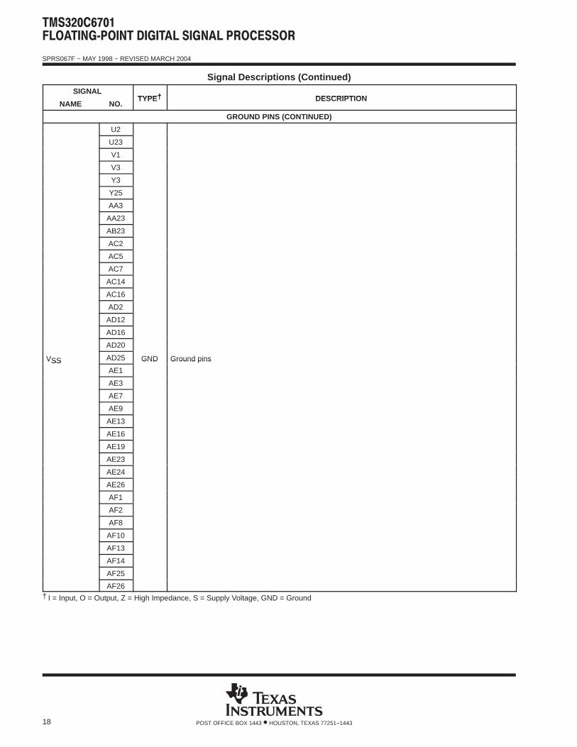
GROUND PINS
A1
A2
A4
A13
A14
A25
A26
B1
B3
B5
B24
B26
C2
C7
C13
C16
C17
C25
D13
VSS D19 GND Ground pinsVSSE3
GND Ground pins
E24
F2
F24
G3
G4
G26
J3
L23
L26
M23
N1
N2
N24
N26
P1
P26
R24
T25† I = Input, O = Output, Z = High Impedance, S = Supply Voltage, GND = Ground
SPRS067F − MAY 1998 − REVISED MARCH 2004
18 POST OFFICE BOX 1443 • HOUSTON, TEXAS 77251−1443
Signal Descriptions (Continued)SIGNAL
TYPE† DESCRIPTIONNAME NO.
TYPE† DESCRIPTION
GROUND PINS (CONTINUED)
U2
U23
V1
V3
Y3
Y25
AA3
AA23
AB23
AC2
AC5
AC7
AC14
AC16
AD2
AD12
AD16
AD20
VSS AD25 GND Ground pinsVSSAE1
GND Ground pins
AE3
AE7
AE9
AE13
AE16
AE19
AE23
AE24
AE26
AF1
AF2
AF8
AF10
AF13
AF14
AF25
AF26† I = Input, O = Output, Z = High Impedance, S = Supply Voltage, GND = Ground
SPRS067F − MAY 1998 − REVISED MARCH 2004
19POST OFFICE BOX 1443 • HOUSTON, TEXAS 77251−1443
Signal Descriptions (Continued)SIGNAL
TYPE† DESCRIPTIONNAME NO.
TYPE† DESCRIPTION
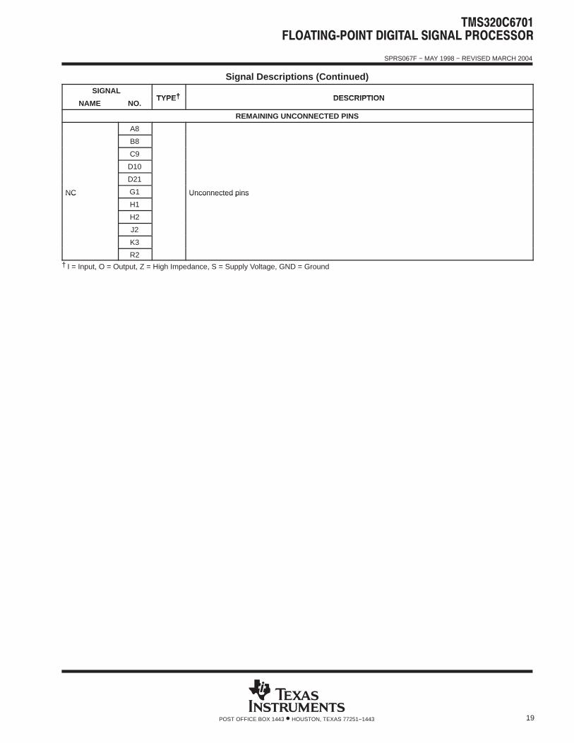
REMAINING UNCONNECTED PINS
A8
B8
C9
D10
D21
NC G1 Unconnected pinsNC
H1
Unconnected pins
H2
J2
K3
R2† I = Input, O = Output, Z = High Impedance, S = Supply Voltage, GND = Ground
SPRS067F − MAY 1998 − REVISED MARCH 2004
20 POST OFFICE BOX 1443 • HOUSTON, TEXAS 77251−1443
development support
TI offers an extensive line of development tools for the TMS320C6000 DSP platform, including tools to evaluatethe performance of the processors, generate code, develop algorithm implementations, and fully integrate anddebug software and hardware modules.
The following products support development of C6000 DSP-based applications:
Software Development Tools:Code Composer Studio Integrated Development Environment (IDE): including EditorC/C++/Assembly Code Generation, and Debug plus additional development toolsScalable, Real-Time Foundation Software (DSP BIOS), which provides the basic run-time target softwareneeded to support any DSP application.
Hardware Development Tools:Extended Development System (XDS) Emulator (supports C6000 DSP multiprocessor system debug)EVM (Evaluation Module)
The TMS320 DSP Development Support Reference Guide (SPRU011) contains information aboutdevelopment-support products for all TMS320 DSP family member devices, including documentation. Seethis document for further information on TMS320 DSP documentation or any TMS320 DSP supportproducts from Texas Instruments. An additional document, the TMS320 Third-Party Support Reference Guide(SPRU052), contains information about TMS320 DSP-related products from other companies in the industry.To receive TMS320 DSP literature, contact the Literature Response Center at 800/477-8924.
For a complete listing of development-support tools for the TMS320C6000 DSP platform, visit the TexasInstruments web site on the Worldwide Web at http://www.ti.com uniform resource locator (URL) and under“Development Tools”, select “Digital Signal Processors”. For information on pricing and availability, contact thenearest TI field sales office or authorized distributor.
Code Composer Studio, XDS, and TMS320 are trademarks of Texas Instruments.

SPRS067F − MAY 1998 − REVISED MARCH 2004
21POST OFFICE BOX 1443 • HOUSTON, TEXAS 77251−1443
device and development-support tool nomenclature
To designate the stages in the product-development cycle, TI assigns prefixes to the part numbers of all TMS320DSP devices and support tools. Each TMS320 DSP family member has one of three prefixes: TMX, TMP, orTMS. Texas Instruments recommends two of three possible prefix designators for support tools: TMDX andTMDS. These prefixes represent evolutionary stages of product development from engineering prototypes(TMX/TMDX) through fully qualified production devices/tools (TMS/TMDS).
Device development evolutionary flow:
TMX Experimental device that is not necessarily representative of the final device’s electricalspecifications
TMP Final silicon die that conforms to the device’s electrical specifications but has not completedquality and reliability verification
TMS Fully qualified production device
Support tool development evolutionary flow:
TMDX Development-support product that has not yet completed Texas Instruments internal qualificationtesting.
TMDS Fully qualified development-support product
TMX and TMP devices and TMDX development-support tools are shipped against the following disclaimer:
“Developmental product is intended for internal evaluation purposes.”
TMS devices and TMDS development-support tools have been characterized fully, and the quality and reliabilityof the device have been demonstrated fully. TI’s standard warranty applies.
Predictions show that prototype devices (TMX or TMP) have a greater failure rate than the standard productiondevices. Texas Instruments recommends that these devices not be used in any production system because theirexpected end-use failure rate still is undefined. Only qualified production devices are to be used.
TI device nomenclature also includes a suffix with the device family name. This suffix indicates the package type(for example, GJC), the temperature range (for example, blank is the default commercial temperature range),and the device speed range in megahertz (for example, -167 is 167 MHz). Table 2 identifies the availableTMS320C6701 devices by their associated orderable part numbers (P/Ns) and gives device-specific orderinginformation (for example, device speeds, core and I/O supply voltage values, and device operating temperatureranges). Figure 4 provides a legend for reading the complete device name for any TMS320 DSP familymember.
Table 2. TMS320C6701 Device P/Ns and Ordering Information
DEVICE ORDERABLE P/N DEVICE SPEEDCVDD
(CORE VOLTAGE)DVDD
(I/O VOLTAGE)
OPERATING CASETEMPERATURE
RANGE
TMSC6701GJC16719V 167 MHz/1 GFLOPS 1.9 V 3.3 V 0C to 90C
TMS320C6701GJC150 150 MHz/900 MFLOPS 1.8 V 3.3 V 0C to 90C
TMS320C6701GJCA120 120 MHz/720 MFLOPS 1.8 V 3.3 V −40C to 105C

SPRS067F − MAY 1998 − REVISED MARCH 2004
22 POST OFFICE BOX 1443 • HOUSTON, TEXAS 77251−1443
device and development-support tool nomenclature (continued)
PREFIX DEVICE SPEED RANGE
TMS 320 C 6701 GJC 167
TMX= Experimental deviceTMP= Prototype deviceTMS= Qualified deviceSMJ = MIL-PRF-38535 (QML)SM = Commercial processing
DEVICE FAMILY320 = TMS320 DSP family
TECHNOLOGY
100 MHz120 MHz150 MHz167 MHz
PACKAGE TYPE †N = Plastic DIPJ = Ceramic DIPJD = Ceramic DIP side-brazedGB = Ceramic PGAFZ = Ceramic CCFN = Plastic leaded CCFD = Ceramic leadless CCPJ = 100-pin plastic EIAJ QFPPQ = 132-pin plastic bumpered QFPPZ = 100-pin plastic TQFPPBK = 128-pin plastic TQFPPGE = 144-pin plastic TQFPGFN = 256-pin plastic BGAGGU = 144-pin plastic BGAGGP = 352-pin plastic BGAGJC = 352-pin plastic BGAGJL = 352-pin plastic BGAGLS = 384-pin plastic BGAGLW = 340-pin plastic BGAGHK = 288-pin plastic MicroStar BGA
C = CMOSE = CMOS EPROMF = CMOS Flash EEPROM
DEVICE’1x DSP:
10 1614 1715
’2x DSP:2526
’2xx DSP:203 206 240204 209
’3x DSP:303132
’4x DSP:4044
’5x DSP:50 5351 5652 57
’54x DSP:541 545542 546543 548
6x DSP:6201 62056202 62116202B 67016203 67116204
† DIP = Dual-In-Line PackagePGA = Pin Grid ArrayCC = Chip CarrierQFP = Quad Flat PackageTQFP = Thin Quad Flat PackageBGA = Ball Grid Array
TEMPERATURE RANGE (DEFAULT: 0 °C TO 90°C)
(A)
Blank = 0°C to 90°C, commercial temperatureA = −40°C to 105°C, extended temperature
200 MHz233 MHz250 MHz300 MHz
Figure 4. TMS320 DSP Device Nomenclature (Including TMS320C6701)
MicroStar BGA is a trademark of Texas Instruments.

SPRS067F − MAY 1998 − REVISED MARCH 2004
23POST OFFICE BOX 1443 • HOUSTON, TEXAS 77251−1443
documentation support
Extensive documentation supports all TMS320 DSP family generations of devices from product announcementthrough applications development. The types of documentation available include: data sheets, such as thisdocument, with design specifications; complete user’s reference guides for all devices; technical briefs;development-support tools; and hardware and software applications. The following is a brief, descriptive list ofsupport documentation specific to the C6x devices:
The TMS320C6000 CPU and Instruction Set Reference Guide (literature number SPRU189) describes theC6000 DSP CPU architecture, instruction set, pipeline, and associated interrupts.
The TMS320C6000 DSP Peripherals Overview Reference Guide (literature number SPRU190) brieflydescribes the functionality of the peripherals available on C6x devices, such as the external memory interface(EMIF), host-port interface (HPI), multichannel buffered serial ports (McBSPs), direct-memory-access (DMA),enhanced direct-memory-access (EDMA) controller, expansion bus (XB), clocking and phase-locked loop(PLL); and power-down modes.
The TMS320C6000 Technical Brief (literature number SPRU197) gives an introduction to the C62x/C67xdevices, associated development tools, and third-party support.
The tools support documentation is electronically available within the Code Composer Studio IntegratedDevelopment Environment (IDE). For a complete listing of C6000 DSP latest documentation, visit the TexasInstruments web site on the Worldwide Web at http://www.ti.com uniform resource locator (URL).

SPRS067F − MAY 1998 − REVISED MARCH 2004
24 POST OFFICE BOX 1443 • HOUSTON, TEXAS 77251−1443
clock PLL
All of the internal C67x clocks are generated from a single source through the CLKIN pin. This source clockeither drives the PLL, which multiplies the source clock in frequency to generate the internal CPU clock, orbypasses the PLL to become the internal CPU clock.
To use the PLL to generate the CPU clock, the external PLL filter circuit must be properly designed. Table 3,Table 4, and Figure 5 show the external PLL circuitry for either x1 (PLL bypass) or x4 PLL multiply modes.Table 3 and Figure 6 show the external PLL circuitry for a system with ONLY x1 (PLL bypass) mode.
To minimize the clock jitter, a single clean power supply should power both the C67x device and the externalclock oscillator circuit. Noise coupling into PLLF directly impacts PLL clock jitter. The minimum CLKIN rise andfall times should also be observed. For the input clock timing requirements, see the input and output clockselectricals section.
Table 3. CLKOUT1 Frequency Ranges †
PLLFREQ3(A9)
PLLFREQ2(D11)
PLLFREQ1(B10)
CLKOUT1 FREQUENCY RANGE(MHZ)
0 0 0 50−140
0 0 1 65−167
0 1 0 130−167† Due to overlap of frequency ranges when choosing the PLLFREQ, more than one frequency range can contain
the CLKOUT1 frequency. Choose the lowest frequency range that includes the desired frequency. For example,for CLKOUT1 = 133 MHz, choose PLLFREQ value of 000b. For CLKOUT1 = 167 MHz, choose PLLFREQ valueof 001b. PLLFREQ values other than 000b, 001b, and 010b are reserved.
Table 4. C6701 PLL Component Selection Table
CLKMODECLKINRANGE(MHz)
CPU CLOCKFREQUENCY(CLKOUT1)
RANGE (MHz)
CLKOUT2RANGE(MHz)
R1(Ω)
C1(nF)
C2(pF)
TYPICALLOCK TIME
(µs)‡
x4 12.5−41.7 50−167 25−83.5 60.4 27 560 75‡ Under some operating conditions, the maximum PLL lock time may vary as much as 150% from the specified typical value. For example, if the
typical lock time is specified as 100 µs, the maximum value may be as long as 250 µs.

SPRS067F − MAY 1998 − REVISED MARCH 2004
25POST OFFICE BOX 1443 • HOUSTON, TEXAS 77251−1443
clock PLL (continued)
AVAILABLE MULTIPLY FACTORS
CLKMODE1 CLKMODE0PLL
MULTIPLYFACTORS
CPU CLOCKFREQUENCY
F(CPUCLOCK)
0 0 x1(BYPASS) 1 x f(CLKIN)
0 1 Reserved Reserved
1 0 Reserved Reserved
1 1 x4 4 x f(CLKIN)
NOTES: A. Keep the lead length and the number of vias between the PLLF pin, the PLLG pin, and R1, C1, and C2 to a minimum. In addition,place all PLL external components (R1, C1, C2, C3, C4, and the EMI Filter) as close to the C6000 DSP device as possible. Forthe best performance, TI recommends that all the PLL external components be on a single side of the board without jumpers,switches, or components other than the ones shown.
B. For reduced PLL jitter, maximize the spacing between switching signals and the PLL external components (R1, C1, C2, C3, C4,and the EMI Filter).
C. The 3.3-V supply for the EMI filter must be from the same 3.3-V power plane supplying the I/O voltage, DVDD.D. EMI filter manufacturer: TDK part number ACF451832-333, 223, 153, 103. Panasonic part number EXCCET103U.
Figure 5. External PLL Circuitry for Either PLL x4 Mode or x1 (Bypass) Mode
CLKMODE0CLKMODE1 PLL
PLLV
CLKIN
LOOP FILTER
PLLCLK
PLLMULT
CLKIN
PLL
G
Internal to C6701
CPUCLOCK
PLL
F
1
0
3.3V(see Table 3)
PLLFREQ1PLLFREQ2PLLFREQ3
NOTES: A. For a system with ONLY PLL x1 (bypass) mode, short the PLLF terminal to the PLLG terminal.B. The 3.3-V supply for the EMI filter must be from the same 3.3-V power plane supplying the I/O voltage, DVDD.
Figure 6. External PLL Circuitry for x1 (Bypass) Mode Only
CLKMODE0CLKMODE1
PLL
PLLV
CLKINLOOP FILTER
PLLCLK
PLLMULT
CLKIN
PLL
G
C2
Internal to C6701
CPUCLOCK
C1R1
3.3V
10 F 0.1 F
PLL
F
EM
I Filt
er
C3 C4
1
0
(see Table 3)PLLFREQ1PLLFREQ2PLLFREQ3

SPRS067F − MAY 1998 − REVISED MARCH 2004
26 POST OFFICE BOX 1443 • HOUSTON, TEXAS 77251−1443
power-down mode logic
Figure 7 shows the power-down mode logic on the C6701.
PWRD
Internal Clock Tree
CPU
IFR
IER
CSR
PD1
PD2
Power-DownLogic
InternalPeripheral
ClockPLL
CLKIN RESET
CLKOUT1
TMS320C6701
PD
(pin)
PD3
InternalPeripheral
Figure 7. Power-Down Mode Logic †
triggering, wake-up, and effects
The power-down modes and their wake-up methods are programmed by setting the PWRD field (bits 15−10)of the control status register (CSR). The PWRD field of the CSR is shown in Figure 8 and described in Table 5.When writing to the CSR, all bits of the PWRD field should be set at the same time. Logic 0 should be used when“writing” to the reserved bit (bit 15) of the PWRD field. The CSR is discussed in detail in the TMS320C6000 CPUand Instruction Set Reference Guide (literature number SPRU189).

SPRS067F − MAY 1998 − REVISED MARCH 2004
27POST OFFICE BOX 1443 • HOUSTON, TEXAS 77251−1443
31 16
15 14 13 12 11 10 9 8
ReservedEnable or
Non-EnabledInterrupt Wake
EnabledInterrupt Wake PD3 PD2 PD1
R/W-0 R/W-0 R/W-0 R/W-0 R/W-0 R/W-0
7 0
Legend: R/W−x = Read/write reset valueNOTE: The shadowed bits are not part of the power-down logic discussion and therefore are not covered here. For information on these other
bit fields in the CSR register, see the TMS320C6000 CPU and Instruction Set Reference Guide (literature number SPRU189).
Figure 8. PWRD Field of the CSR Register
Power-down mode PD1 takes effect eight to nine clock cycles after the instruction that sets the PWRD bits in theCSR.
If PD1 mode is terminated by a non-enabled interrupt, the program execution returns to the instruction where PD1took effect. If PD1 mode is terminated by an enabled interrupt, the interrupt service routine will be executed first,then the program execution returns to the instruction where PD1 took effect. The GIE bit in CSR and the NMIEbit in the interrupt enable register (IER) must also be set in order for the interrupt service routine to execute;otherwise, execution returns to the instruction where PD1 took effect upon PD1 mode termination by an enabledinterrupt.
PD2 and PD3 modes can only be aborted by device reset. Table 5 summarizes all the power-down modes.

SPRS067F − MAY 1998 − REVISED MARCH 2004
28 POST OFFICE BOX 1443 • HOUSTON, TEXAS 77251−1443
Table 5. Characteristics of the Power-Down Modes
PRWD FIELD(BITS 15−10)
POWER-DOWNMODE WAKE-UP METHOD EFFECT ON CHIP’S OPERATION
000000 No power-down — —
001001 PD1 Wake by an enabled interrupt CPU halted (except for the interrupt logic)Power-down mode blocks the internal clock inputs at the
010001 PD1Wake by an enabled ornon-enabled interrupt
Power-down mode blocks the internal clock inputs at theboundary of the CPU, preventing most of the CPU’s logic fromswitching. During PD1, DMA transactions can proceed betweenperipherals and internal memory.
011010 PD2† Wake by a device reset
Output clock from PLL is halted, stopping the internal clockstructure from switching and resulting in the entire chip beinghalted. All register and internal RAM contents are preserved. Allfunctional I/O “freeze” in the last state when the PLL clock isturned off.
011100 PD3† Wake by a device reset
Input clock to the PLL stops generating clocks. All register andinternal RAM contents are preserved. All functional I/O “freeze” inthe last state when the PLL clock is turned off. Following reset, thePLL needs time to re-lock, just as it does following power-up.Wake-up from PD3 takes longer than wake-up from PD2 becausethe PLL needs to be re-locked.
All others Reserved — —
† When entering PD2 and PD3, all functional I/O remains in the previous state. However, for peripherals which are asynchronous in nature orperipherals with an external clock source, output signals may transition in response to stimulus on the inputs. Under these conditions,peripherals will not operate according to specifications.

SPRS067F − MAY 1998 − REVISED MARCH 2004
29POST OFFICE BOX 1443 • HOUSTON, TEXAS 77251−1443
absolute maximum ratings over operating case temperature range (unless otherwise noted) † Supply voltage range, CVDD (see Note 1) −0.3 V to 2.3 V. . . . . . . . . . . . . . . . . . . . . . . . . . . . . . . . . . . . . . . . . . . . Supply voltage range, DVDD (see Note 1) −0.3 V to 4 V. . . . . . . . . . . . . . . . . . . . . . . . . . . . . . . . . . . . . . . . . . . . . Input voltage range −0.3 V to 4 V. . . . . . . . . . . . . . . . . . . . . . . . . . . . . . . . . . . . . . . . . . . . . . . . . . . . . . . . . . . . . . . . . Output voltage range −0.3 V to 4 V. . . . . . . . . . . . . . . . . . . . . . . . . . . . . . . . . . . . . . . . . . . . . . . . . . . . . . . . . . . . . . . Operating case temperature range, TC (Default) 0C to 90C. . . . . . . . . . . . . . . . . . . . . . . . . . . . . . . . . . . .
(A Version) −40C to 105C. . . . . . . . . . . . . . . . . . . . . . . . . . . . . . . Storage temperature range, Tstg −55C to 150C. . . . . . . . . . . . . . . . . . . . . . . . . . . . . . . . . . . . . . . . . . . . . . .
† Stresses beyond those listed under “absolute maximum ratings” may cause permanent damage to the device. These are stress ratings only, andfunctional operation of the device at these or any other conditions beyond those indicated under “recommended operating conditions” is notimplied. Exposure to absolute-maximum-rated conditions for extended periods may affect device reliability.
NOTE 1: All voltage values are with respect to VSS.
recommended operating conditions
MIN NOM MAX UNIT
CVDD Supply voltage, Core‡6701-120, -150 1.71 1.8 1.89 V
CVDD Supply voltage, Core‡6701-167 only 1.81 1.9 1.99 V
DVDD Supply voltage, I/O‡ 3.14 3.30 3.46 V
VSS Supply ground 0 0 0 V
VIH High-level input voltage 2.0 V
VIL Low-level input voltage 0.8 V
IOH High-level output current −12 mA
IOL Low-level output current 12 mA
TC Case temperatureDefault 0 90 C
TC Case temperatureA Version −40 105 C
‡ TI DSP’s do not require specific power sequencing between the core supply and the I/O supply. However, systems should be designed to ensurethat neither supply is powered up for extended periods of time if the other supply is below the proper operating voltage. Excessive exposure tothese conditions can adversely affect the long term reliability of the device. System-level concerns such as bus contention may require supplysequencing to be implemented. In this case, the core supply should be powered up at the same time as, or prior to (and powered down after),the I/O buffers. For additional power supply sequencing information, see the Power Supply Sequencing Solutions For Dual Supply Voltage DSPsapplication report (literature number SLVA073).

SPRS067F − MAY 1998 − REVISED MARCH 2004
30 POST OFFICE BOX 1443 • HOUSTON, TEXAS 77251−1443
electrical characteristics over recommended ranges of supply voltage and operating casetemperature (unless otherwise noted)
PARAMETER TEST CONDITIONS MIN TYP MAX UNIT
VOH High-level output voltage DVDD = MIN, IOH = MAX 2.4 V
VOL Low-level output voltage DVDD = MIN, IOL = MAX 0.6 V
II Input current† VI = VSS to DVDD ±10 uA
IOZ Off-state output current VO = DVDD or 0 V ±10 uA
IDD2V Supply current, CPU + CPU memory access‡CVDD = NOM, CPU clock = 150 MHz 470
mAIDD2V Supply current, CPU + CPU memory access‡CVDD = NOM, CPU clock = 120 MHz 380
mA
IDD2V Supply current, peripherals‡CVDD = NOM, CPU clock = 150 MHz 250
mAIDD2V Supply current, peripherals‡CVDD = NOM, CPU clock = 120 MHz 200
mA
IDD3V Supply current, I/O pins‡DVDD = NOM, CPU clock = 150 MHz 85
mAIDD3V Supply current, I/O pins‡DVDD = NOM, CPU clock = 120 MHz 70
mA
Ci Input capacitance 10 pF
Co Output capacitance 10 pF
† TMS and TDI are not included due to internal pullups.TRST is not included due to internal pulldown.
‡ Measured with average activity (50% high / 50% low power). For more detailed information on CPU/peripheral/I/O activity, see the TMS320C6000Power Consumption Summary application report (literature number SPRA486).

SPRS067F − MAY 1998 − REVISED MARCH 2004
31POST OFFICE BOX 1443 • HOUSTON, TEXAS 77251−1443
PARAMETER MEASUREMENT INFORMATION
Tester PinElectronics
Vref
IOL
CT = 30 pF†
IOH
OutputUnderTest
50 Ω
† Typical distributed load circuit capacitance.
signal-transition levels
All input and output timing parameters are referenced to 1.5 V for both “0” and “1” logic levels.
Vref = 1.5 V
Figure 9. Input and Output Voltage Reference Levels for ac Timing Measurements

SPRS067F − MAY 1998 − REVISED MARCH 2004
32 POST OFFICE BOX 1443 • HOUSTON, TEXAS 77251−1443
INPUT AND OUTPUT CLOCKS
timing requirements for CLKIN (C6701-150, -167 devices only) †‡ (see Figure 10)
C6701-150 C6701-167
NO. CLKMODE = x4 CLKMODE = x1 CLKMODE = x4 CLKMODE = x1 UNITNO.
MIN MAX MIN MAX MIN MAX MIN MAX
UNIT
1 tc(CLKIN) Cycle time, CLKIN 26.7 6.7 24 6 ns
2 tw(CLKINH)Pulse duration,CLKIN high
0.4C 0.45C 0.4C 0.45C ns
3 tw(CLKINL)Pulse duration,CLKIN low
0.4C 0.45C 0.4C 0.45C ns
4 tt(CLKIN) Transition time, CLKIN 5 0.6 5 0.6 ns
† The reference points for the rise and fall transitions are measured at 20% and 80%, respectively, of VIH.‡ C = CLKIN cycle time in ns. For example, when CLKIN frequency is 10 MHz, use C = 100 ns.
timing requirements for CLKIN (C6701-120 device only) †‡ (see Figure 10)
C6701-120
NO. CLKMODE = x4 CLKMODE = x1 UNITNO.
MIN MAX MIN MAX
UNIT
1 tc(CLKIN) Cycle time, CLKIN 33.3 8.3 ns
2 tw(CLKINH) Pulse duration, CLKIN high 0.4C 0.45C ns
3 tw(CLKINL) Pulse duration, CLKIN low 0.4C 0.45C ns
4 tt(CLKIN) Transition time, CLKIN 5 0.6 ns
† The reference points for the rise and fall transitions are measured at 20% and 80%, respectively, of VIH.‡ C = CLKIN cycle time in ns. For example, when CLKIN frequency is 10 MHz, use C = 100 ns.
CLKIN
1
2
3
4
4
Figure 10. CLKIN Timings

SPRS067F − MAY 1998 − REVISED MARCH 2004
33POST OFFICE BOX 1443 • HOUSTON, TEXAS 77251−1443
INPUT AND OUTPUT CLOCKS (CONTINUED)
switching characteristics for CLKOUT1 †‡ (see Figure 11)
NO. PARAMETER
C6701-120C6701-150C6701-167 UNITNO. PARAMETER
CLKMODE = X4 CLKMODE = X1UNIT
MIN MAX MIN MAX
1 tc(CKO1) Cycle time, CLKOUT1 P − 0.7 P + 0.7 P − 0.7 P + 0.7 ns
2 tw(CKO1H) Pulse duration, CLKOUT1 high (P/2) − 0.5 (P/2) + 0.5 PH − 0.5 PH + 0.5 ns
3 tw(CKO1L) Pulse duration, CLKOUT1 low (P/2) − 0.5 (P/2) + 0.5 PL − 0.5 PL + 0.5 ns
4 tt(CKO1) Transition time, CLKOUT1 0.6 0.6 ns
† P = 1/CPU clock frequency in nanoseconds (ns).‡ PH is the high period of CLKIN in ns and PL is the low period of CLKIN in ns.
CLKOUT1
1
3
4
4
2
Figure 11. CLKOUT1 Timings
switching characteristics for CLKOUT2 § (see Figure 12)
NO. PARAMETER
C6701-120C6701-150C6701-167 UNIT
MIN MAX
1 tc(CKO2) Cycle time, CLKOUT2 2P − 0.7 2P + 0.7 ns
2 tw(CKO2H) Pulse duration, CLKOUT2 high P − 0.7 P + 0.7 ns
3 tw(CKO2L) Pulse duration, CLKOUT2 low P − 0.7 P + 0.7 ns
4 tt(CKO2) Transition time, CLKOUT2 0.6 ns
§ P = 1/CPU clock frequency in ns.
CLKOUT2
1
2
3
4
4
Figure 12. CLKOUT2 Timings

SPRS067F − MAY 1998 − REVISED MARCH 2004
34 POST OFFICE BOX 1443 • HOUSTON, TEXAS 77251−1443
INPUT AND OUTPUT CLOCKS (CONTINUED)
SDCLK, SSCLK timing parameters
SDCLK timing parameters are the same as CLKOUT2 parameters.
SSCLK timing parameters are the same as CLKOUT1 or CLKOUT2 parameters, depending on SSCLKconfiguration.
switching characteristics for the relation of SSCLK, SDCLK, and CLKOUT2 to CLKOUT1(see Figure 13)
NO. PARAMETER
C6701-120C6701-150C6701-167 UNIT
MIN MAX
1 td(CKO1-SSCLK) Delay time, CLKOUT1 edge to SSCLK edge −0.8 3.4 ns
2 td(CKO1-SSCLK1/2) Delay time, CLKOUT1 edge to SSCLK edge (1/2 clock rate) −1.0 3.0 ns
3 td(CKO1-CKO2) Delay time, CLKOUT1 edge to CLKOUT2 edge −1.5 2.5 ns
4 td(CKO1-SDCLK) Delay time, CLKOUT1 edge to SDCLK edge −1.5 1.9 ns
4
3
2
1
CLKOUT1
SSCLK
SSCLK (1/2rate)
CLKOUT2
SDCLK
Figure 13. Relation of CLKOUT2, SDCLK, and SSCLK to CLKOUT1

SPRS067F − MAY 1998 − REVISED MARCH 2004
35POST OFFICE BOX 1443 • HOUSTON, TEXAS 77251−1443
ASYNCHRONOUS MEMORY TIMING
timing requirements for asynchronous memory cycles † (see Figure 14 and Figure 15)
NO.
C6701-120C6701-150C6701-167 UNIT
MIN MAX
6 tsu(EDV-CKO1H) Setup time, read EDx valid before CLKOUT1 high 4.5 ns
7 th(CKO1H-EDV) Hold time, read EDx valid after CLKOUT1 high 1.5 ns
10 tsu(ARDY-CKO1H) Setup time, ARDY valid before CLKOUT1 high 3.5 ns
11 th(CKO1H-ARDY) Hold time, ARDY valid after CLKOUT1 high 1.5 ns
† To ensure data setup time, simply program the strobe width wide enough. ARDY is internally synchronized. If ARDY does meet setup or holdtime, it may be recognized in the current cycle or the next cycle. Thus, ARDY can be an asynchronous input.
switching characteristics for asynchronous memory cycles ‡ (see Figure 14 and Figure 15)
NO. PARAMETER
C6701-120C6701-150C6701-167 UNIT
MIN MAX
1 td(CKO1H-CEV) Delay time, CLKOUT1 high to CEx valid −1.0 4.5 ns
2 td(CKO1H-BEV) Delay time, CLKOUT1 high to BEx valid 4.5 ns
3 td(CKO1H-BEIV) Delay time, CLKOUT1 high to BEx invalid −1.0 ns
4 td(CKO1H-EAV) Delay time, CLKOUT1 high to EAx valid 4.5 ns
5 td(CKO1H-EAIV) Delay time, CLKOUT1 high to EAx invalid −1.0 ns
8 td(CKO1H-AOEV) Delay time, CLKOUT1 high to AOE valid −1.0 4.5 ns
9 td(CKO1H-AREV) Delay time, CLKOUT1 high to ARE valid −0.5 4.5 ns
12 td(CKO1H-EDV) Delay time, CLKOUT1 high to EDx valid 4.5 ns
13 td(CKO1H-EDIV) Delay time, CLKOUT1 high to EDx invalid −1.0 ns
14 td(CKO1H-AWEV) Delay time, CLKOUT1 high to AWE valid −1.0 4.5 ns
‡ The minimum delay is also the minimum output hold after CLKOUT1 high.

SPRS067F − MAY 1998 − REVISED MARCH 2004
36 POST OFFICE BOX 1443 • HOUSTON, TEXAS 77251−1443
ASYNCHRONOUS MEMORY TIMING (CONTINUED)
111110 10
99
88
76
54
32
11
CLKOUT1
CEx
BE[3:0]
EA[21:2]
ED[31:0]
AOE
ARE
AWE
ARDY
Setup = 2 Strobe = 5 Not ready = 2HOLD = 1
Figure 14. Asynchronous Memory Read Timing
1110
1110
1414
1312
54
32
11
CLKOUT1
CEx
BE[3:0]
EA[21:2]
ED[31:0]
AOE
ARE
AWE
ARDY
Setup = 2 Strobe = 5 Not ready = 2HOLD = 1
Figure 15. Asynchronous Memory Write Timing

SPRS067F − MAY 1998 − REVISED MARCH 2004
37POST OFFICE BOX 1443 • HOUSTON, TEXAS 77251−1443
SYNCHRONOUS-BURST MEMORY TIMING
timing requirements for synchronous-burst SRAM cycles (full-rate SSCLK) (see Figure 16)
NO.’C6701-120
C6701-150C6701-167 UNITNO.
MIN MAX MIN MAXUNIT
7 tsu(EDV-SSCLKH) Setup time, read EDx valid before SSCLK high 2.0 2.0 ns
8 th(SSCLKH-EDV) Hold time, read EDx valid after SSCLK high 2.9 2.1 ns
switching characteristics for synchronous-burst SRAM cycles † (full-rate SSCLK)(see Figure 16 and Figure 17)
NO. PARAMETER’C6701-120
C6701-150C6701-167 UNITNO. PARAMETER
MIN MAX MIN MAXUNIT
1 tosu(CEV-SSCLKH) Output setup time, CEx valid before SSCLK high 0.5P − 1.3 0.5P − 1.3 ns
2 toh(SSCLKH-CEV) Output hold time, CEx valid after SSCLK high 0.5P − 2.9 0.5P − 2.3 ns
3 tosu(BEV-SSCLKH) Output setup time, BEx valid before SSCLK high 0.5P − 1.3 0.5P − 1.6 ns
4 toh(SSCLKH-BEIV) Output hold time, BEx invalid after SSCLK high 0.5P − 2.9 0.5P − 2.3 ns
5 tosu(EAV-SSCLKH) Output setup time, EAx valid before SSCLK high 0.5P − 1.3 0.5P − 1.7 ns
6 toh(SSCLKH-EAIV) Output hold time, EAx invalid after SSCLK high 0.5P − 2.9 0.5P − 2.3 ns
9 tosu(ADSV-SSCLKH) Output setup time, SSADS valid before SSCLK high 0.5P − 1.3 0.5P − 1.3 ns
10 toh(SSCLKH-ADSV) Output hold time, SSADS valid after SSCLK high 0.5P − 2.9 0.5P − 2.3 ns
11 tosu(OEV-SSCLKH) Output setup time, SSOE valid before SSCLK high 0.5P − 1.3 0.5P − 1.3 ns
12 toh(SSCLKH-OEV) Output hold time, SSOE valid after SSCLK high 0.5P − 2.9 0.5P − 2.3 ns
13 tosu(EDV-SSCLKH) Output setup time, EDx valid before SSCLK high 0.5P − 1.3 0.5P − 1.3 ns
14 toh(SSCLKH-EDIV) Output hold time, EDx invalid after SSCLK high 0.5P − 2.9 0.5P − 2.3 ns
15 tosu(WEV-SSCLKH) Output setup time, SSWE valid before SSCLK high 0.5P − 1.3 0.5P − 1.3 ns
16 toh(SSCLKH-WEV) Output hold time, SSWE valid after SSCLK high 0.5P − 2.9 0.5P − 2.3 ns
† When the PLL is used (CLKMODE x4), P = 1/CPU clock frequency in ns. For example, when running parts at 167 MHz, use P = 6 ns.For CLKMODE x1, 0.5P is defined as PH (pulse duration of CLKIN high) for all output setup times; 0.5P is defined as PL (pulse duration of CLKINlow) for all output hold times.

SPRS067F − MAY 1998 − REVISED MARCH 2004
38 POST OFFICE BOX 1443 • HOUSTON, TEXAS 77251−1443
SYNCHRONOUS-BURST MEMORY TIMING (CONTINUED)
BE1 BE2 BE3 BE4
A1 A2 A3 A4
Q1 Q2 Q3 Q4
1211
109
87
65
43
21
SSCLK
CEx
BE[3:0]
EA[21:2]
ED[31:0]
SSADS
SSOE
SSWE
Figure 16. SBSRAM Read Timing (Full-Rate SSCLK)
BE1 BE2 BE3 BE4
A1 A2 A3 A4
D1 D2 D3 D4
1615
109
1413
65
43
21
SSCLK
CEx
BE[3:0]
EA[21:2]
ED[31:0]
SSADS
SSOE
SSWE
Figure 17. SBSRAM Write Timing (Full-Rate SSCLK)

SPRS067F − MAY 1998 − REVISED MARCH 2004
39POST OFFICE BOX 1443 • HOUSTON, TEXAS 77251−1443
SYNCHRONOUS-BURST MEMORY TIMING (CONTINUED)
timing requirements for synchronous-burst SRAM cycles (half-rate SSCLK) (see Figure 18)
NO.
C6701-120C6701-150C6701-167 UNIT
MIN MAX
7 tsu(EDV-SSCLKH) Setup time, read EDx valid before SSCLK high 3.6 ns
8 th(SSCLKH-EDV) Hold time, read EDx valid after SSCLK high 1.5 ns
switching characteristics for synchronous-burst SRAM cycles † (half-rate SSCLK)(see Figure 18 and Figure 19)
NO. PARAMETERC6701-120
C6701-150C6701-167 UNITNO. PARAMETER
MIN MAX MIN MAXUNIT
1 tosu(CEV-SSCLKH) Output setup time, CEx valid before SSCLK high 1.5P − 4.5 1.5P − 4.5 ns
2 toh(SSCLKH-CEV) Output hold time, CEx valid after SSCLK high 0.5P − 2.5 0.5P − 2 ns
3 tosu(BEV-SSCLKH) Output setup time, BEx valid before SSCLK high 1.5P − 4.5 1.5P − 4.5 ns
4 toh(SSCLKH-BEIV) Output hold time, BEx invalid after SSCLK high 0.5P − 2.5 0.5P − 2 ns
5 tosu(EAV-SSCLKH) Output setup time, EAx valid before SSCLK high 1.5P − 4.5 1.5P − 4.5 ns
6 toh(SSCLKH-EAIV) Output hold time, EAx invalid after SSCLK high 0.5P − 2.5 0.5P − 2 ns
9 tosu(ADSV-SSCLKH) Output setup time, SSADS valid before SSCLK high 1.5P − 4.5 1.5P − 4.5 ns
10 toh(SSCLKH-ADSV) Output hold time, SSADS valid after SSCLK high 0.5P − 2.5 0.5P − 2 ns
11 tosu(OEV-SSCLKH) Output setup time, SSOE valid before SSCLK high 1.5P − 4.5 1.5P − 4.5 ns
12 toh(SSCLKH-OEV) Output hold time, SSOE valid after SSCLK high 0.5P − 2.5 0.5P − 2 ns
13 tosu(EDV-SSCLKH) Output setup time, EDx valid before SSCLK high 1.5P − 4.5 1.5P − 4.5 ns
14 toh(SSCLKH-EDIV) Output hold time, EDx invalid after SSCLK high 0.5P − 2.5 0.5P − 2 ns
15 tosu(WEV-SSCLKH) Output setup time, SSWE valid before SSCLK high 1.5P − 4.5 1.5P − 4.5 ns
16 toh(SSCLKH-WEV) Output hold time, SSWE valid after SSCLK high 0.5P − 2.5 0.5P − 2 ns
† When the PLL is used (CLKMODE x4), P = 1/CPU clock frequency in ns. For example, when running parts at 167 MHz, use P = 6 ns.For CLKMODE x1:
1.5P = P + PH, where P = 1/CPU clock frequency, and PH = pulse duration of CLKIN high.0.5P = PL, where PL = pulse duration of CLKIN low.

SPRS067F − MAY 1998 − REVISED MARCH 2004
40 POST OFFICE BOX 1443 • HOUSTON, TEXAS 77251−1443
SYNCHRONOUS-BURST MEMORY TIMING (CONTINUED)
SSCLK
CEx
BE[3:0]
EA[21:2]
ED[31:0]
SSADS
SSOE
SSWE
BE1 BE2 BE3 BE4
A1 A2 A3 A4
Q1 Q2 Q3 Q4
1211
109
65
43
21
87
Figure 18. SBSRAM Read Timing (1/2 Rate SSCLK)
SSCLK
CEx
BE[3:0]
EA[21:2]
ED[31:0]
SSADS
SSOE
SSWE
BE1 BE2 BE3 BE4
A1 A2 A3 A4
Q1 Q2 Q3 Q4
1615
109
1413
65
43
21
Figure 19. SBSRAM Write Timing (1/2 Rate SSCLK)

SPRS067F − MAY 1998 − REVISED MARCH 2004
41POST OFFICE BOX 1443 • HOUSTON, TEXAS 77251−1443
SYNCHRONOUS DRAM TIMING
timing requirements for synchronous DRAM cycles (see Figure 20)
NO.
C6701-120C6701-150C6701-167 UNIT
MIN MAX
7 tsu(EDV-SDCLKH) Setup time, read EDx valid before SDCLK high 1.8 ns
8 th(SDCLKH-EDV) Hold time, read EDx valid after SDCLK high 3 ns
switching characteristics for synchronous DRAM cycles † (see Figure 20−Figure 25)
NO. PARAMETERC6701-120
C6701-150C6701-167 UNITNO. PARAMETER
MIN MAX MIN MAXUNIT
1 tosu(CEV-SDCLKH) Output setup time, CEx valid before SDCLK high 1.5P − 4 1.5P − 4 ns
2 toh(SDCLKH-CEV) Output hold time, CEx valid after SDCLK high 0.5P − 1.9 0.5P − 1.5 ns
3 tosu(BEV-SDCLKH) Output setup time, BEx valid before SDCLK high 1.5P − 4 1.5P − 4 ns
4 toh(SDCLKH-BEIV) Output hold time, BEx invalid after SDCLK high 0.5P − 1.9 0.5P − 1.5 ns
5 tosu(EAV-SDCLKH) Output setup time, EAx valid before SDCLK high 1.5P − 4 1.5P − 4 ns
6 toh(SDCLKH-EAIV) Output hold time, EAx invalid after SDCLK high 0.5P − 1.9 0.5P − 1.5 ns
9 tosu(SDCAS-SDCLKH) Output setup time, SDCAS valid before SDCLK high 1.5P − 4 1.5P − 4 ns
10 toh(SDCLKH-SDCAS) Output hold time, SDCAS valid after SDCLK high 0.5P − 1.9 0.5P − 1.5 ns
11 tosu(EDV-SDCLKH) Output setup time, EDx valid before SDCLK high 1.5P − 4 1.5P − 4 ns
12 toh(SDCLKH-EDIV) Output hold time, EDx invalid after SDCLK high 0.5P − 1.9 0.5P − 1.5 ns
13 tosu(SDWE-SDCLKH) Output setup time, SDWE valid before SDCLK high 1.5P − 4 1.5P − 4 ns
14 toh(SDCLKH-SDWE) Output hold time, SDWE valid after SDCLK high 0.5P − 1.9 0.5P − 1.5 ns
15 tosu(SDA10V-SDCLKH) Output setup time, SDA10 valid before SDCLK high 1.5P − 4 1.5P − 4 ns
16 toh(SDCLKH-SDA10IV) Output hold time, SDA10 invalid after SDCLK high 0.5P − 1.9 0.5P − 1.5 ns
17 tosu(SDRAS-SDCLKH) Output setup time, SDRAS valid before SDCLK high 1.5P − 4 1.5P − 4 ns
18 toh(SDCLKH-SDRAS) Output hold time, SDRAS valid after SDCLK high 0.5P − 1.9 0.5P − 1.5 ns
† When the PLL is used (CLKMODE x4), P = 1/CPU clock frequency in ns. For example, when running parts at 167 MHz, use P = 6 ns.For CLKMODE x1:
1.5P = P + PH, where P = 1/CPU clock frequency, and PH = pulse duration of CLKIN high.0.5P = PL, where PL = pulse duration of CLKIN low.

SPRS067F − MAY 1998 − REVISED MARCH 2004
42 POST OFFICE BOX 1443 • HOUSTON, TEXAS 77251−1443
SYNCHRONOUS DRAM TIMING (CONTINUED)
SDCLK
CEx
BE[3:0]
EA[15:2]
ED[31:0]
SDA10
SDRAS
SDCAS
SDWE
BE1 BE2 BE3
CA1 CA2 CA3
D1 D2 D3
109
1615
65
43
21
87
READREADREAD
Figure 20. Three SDRAM Read Commands
SDCLK
CEx
BE[3:0]
EA[15:2]
ED[31:0]
SDA10
SDRAS
SDCAS
SDWE
BE1 BE2 BE3
CA1 CA2 CA3
D1 D2 D3
1413
109
1615
1211
65
43
21
WRITEWRITEWRITE
Figure 21. Three SDRAM Write Commands

SPRS067F − MAY 1998 − REVISED MARCH 2004
43POST OFFICE BOX 1443 • HOUSTON, TEXAS 77251−1443
SYNCHRONOUS DRAM TIMING (CONTINUED)
SDCLK
CEx
BE[3:0]
EA[15:2]
ED[31:0]
SDA10
SDRAS
SDCAS
SDWE
Bank Activate/Row Address
Row Address
1817
15
5
21
ACTV
Figure 22. SDRAM ACTV Command
SDCLK
CEx
BE[3:0]
EA[15:2]
ED[31:0]
SDA10
SDRAS
SDCAS
SDWE
14
18
16
2
15
1
17
13
DCAB
Figure 23. SDRAM DCAB Command

SPRS067F − MAY 1998 − REVISED MARCH 2004
44 POST OFFICE BOX 1443 • HOUSTON, TEXAS 77251−1443
SYNCHRONOUS DRAM TIMING (CONTINUED)
SDCLK
CEx
BE[3:0]
EA[15:2]
ED[31:0]
SDA10
SDRAS
SDCAS
SDWE
109
1817
21
REFR
Figure 24. SDRAM REFR Command
SDCLK
CEx
BE[3:0]
EA[15:2]
ED[31:0]
SDA10
SDRAS
SDCAS
SDWE
MRS Value
14
10
18
6
21
5
17
9
13
MRS
Figure 25. SDRAM MRS Command

SPRS067F − MAY 1998 − REVISED MARCH 2004
45POST OFFICE BOX 1443 • HOUSTON, TEXAS 77251−1443
HOLD/HOLDA TIMING
timing requirements for the hold/hold acknowledge cycles † (see Figure 26)
NO.
C6701-120C6701-150C6701-167 UNIT
MIN MAX
1 tsu(HOLDH-CKO1H) Setup time, HOLD high before CLKOUT1 high 5 ns
2 th(CKO1H-HOLDL) Hold time, HOLD low after CLKOUT1 high 2 ns
† HOLD is synchronized internally. Therefore, if setup and hold times are not met, it will either be recognized in the current cycle or in the next cycle.Thus, HOLD can be an asynchronous input.
switching characteristics for the hold/hold acknowledge cycles ‡ (see Figure 26)
NO. PARAMETER
C6701-120C6701-150C6701-167 UNIT
MIN MAX
3 tR(HOLDL-EMHZ) Response time, HOLD low to EMIF high impedance 4P § ns
4 tR(EMHZ-HOLDAL) Response time, EMIF high impedance to HOLDA low 2P ns
5 tR(HOLDH-HOLDAH) Response time, HOLD high to HOLDA high 4P 7P ns
6 td(CKO1H-HOLDAL) Delay time, CLKOUT1 high to HOLDA valid 1 8 ns
7 td(CKO1H-BHZ) Delay time, CLKOUT1 high to EMIF Bus high impedance¶ 1 8 ns
8 td(CKO1H-BLZ) Delay time, CLKOUT1 high to EMIF Bus low impedance¶ 1 12 ns
9 tR(HOLDH-BLZ) Response time, HOLD high to EMIF Bus low impedance¶ 3P 6P ns
‡ P = 1/CPU clock frequency in ns. For example, when running parts at 167 MHz, use P = 6 ns.§ All pending EMIF transactions are allowed to complete before HOLDA is asserted. The worst cases for this is an asynchronous read or write
with external ARDY used or a minimum of eight consecutive SDRAM reads or writes when RBTR8 = 1. If no bus transactions are occurring, thenthe minimum delay time can be achieved. Also, bus hold can be indefinitely delayed by setting the NOHOLD = 1.
¶ EMIF Bus consists of CE[3:0], BE[3:0], ED[31:0], EA[21:2], ARE, AOE, AWE, SSADS, SSOE, SSWE, SDA10, SDRAS, SDCAS, and SDWE.
DSP Owns Bus External Requester DSP Owns Bus
’C6701 Ext Req ’C67018
7
34
66
12
CLKOUT1
HOLD
HOLDA
EMIF Bus †
1
59
2
† EMIF Bus consists of CE[3:0], BE[3:0], ED[31:0], EA[21:2], ARE, AOE, AWE, SSADS, SSOE, SSWE, SDA10, SDRAS, SDCAS, and SDWE.
Figure 26. HOLD /HOLDA Timing

SPRS067F − MAY 1998 − REVISED MARCH 2004
46 POST OFFICE BOX 1443 • HOUSTON, TEXAS 77251−1443
RESET TIMING
timing requirements for reset (see Figure 27)
NO.
C6701-120C6701-150C6701-167 UNIT
MIN MAX
1 tw(RESET)Width of the RESET pulse (PLL stable)† 10
CLKOUT1cycles1 tw(RESET)
Width of the RESET pulse (PLL needs to sync up)‡ 250 µs
† This parameter applies to CLKMODE x1 when CLKIN is stable and applies to CLKMODE x4 when CLKIN and PLL are stable.‡ This parameter only applies to CLKMODE x4. The RESET signal is not connected internally to the clock PLL circuit. The PLL, however, may
need up to 250 µs to stabilize following device powerup or after PLL configuration has been changed. During that time, RESET must be assertedto ensure proper device operation. See the clock PLL section for PLL lock times.
switching characteristics during reset §¶ (see Figure 27)
NO. PARAMETER
C6701-120C6701-150C6701-167 UNIT
MIN MAX
2 tR(RESET) Response time to change of value in RESET signal 1CLKOUT1
cycles
3 td(CKO1H-CKO2IV) Delay time, CLKOUT1 high to CLKOUT2 invalid −1 ns
4 td(CKO1H-CKO2V) Delay time, CLKOUT1 high to CLKOUT2 valid 10 ns
5 td(CKO1H-SDCLKIV) Delay time, CLKOUT1 high to SDCLK invalid −1 ns
6 td(CKO1H-SDCLKV) Delay time, CLKOUT1 high to SDCLK valid 10 ns
7 td(CKO1H-SSCKIV) Delay time, CLKOUT1 high to SSCLK invalid −1 ns
8 td(CKO1H-SSCKV) Delay time, CLKOUT1 high to SSCLK valid 10 ns
9 td(CKO1H-LOWIV) Delay time, CLKOUT1 high to low group invalid −1 ns
10 td(CKO1H-LOWV) Delay time, CLKOUT1 high to low group valid 10 ns
11 td(CKO1H-HIGHIV) Delay time, CLKOUT1 high to high group invalid −1 ns
12 td(CKO1H-HIGHV) Delay time, CLKOUT1 high to high group valid 10 ns
13 td(CKO1H-ZHZ) Delay time, CLKOUT1 high to Z group high impedance −1 ns
14 td(CKO1H-ZV) Delay time, CLKOUT1 high to Z group valid 10 ns
§ Low group consists of: IACK, INUM[3:0], DMAC[3:0], PD, TOUT0, and TOUT1.High group consists of: HINT.Z group consists of: EA[21:2], ED[31:0], CE[3:0], BE[3:0], ARE, AWE, AOE, SSADS, SSOE, SSWE, SDA10, SDRAS, SDCAS,
SDWE, HD[15:0], CLKX0, CLKX1, FSX0, FSX1, DX0, DX1, CLKR0, CLKR1, FSR0, and FSR1.¶ HRDY is gated by input HCS.
If HCS = 0 at device reset, HRDY belongs to the high group.If HCS = 1 at device reset, HRDY belongs to the low group.

SPRS067F − MAY 1998 − REVISED MARCH 2004
47POST OFFICE BOX 1443 • HOUSTON, TEXAS 77251−1443
RESET TIMING (CONTINUED)
122
1413
1211
109
87
65
43
CLKOUT1
RESET
CLKOUT2
SDCLK
SSCLK
LOW GROUP†‡
HIGH GROUP†‡
Z GROUP†‡
† Low group consists of: IACK, INUM[3:0], DMAC[3:0], PD, TOUT0, and TOUT1.High group consists of: HINT.Z group consists of: EA[21:2], ED[31:0], CE[3:0], BE[3:0], ARE, AWE, AOE, SSADS, SSOE, SSWE, SDA10, SDRAS, SDCAS,
SDWE, HD[15:0], CLKX0, CLKX1, FSX0, FSX1, DX0, DX1, CLKR0, CLKR1, FSR0, and FSR1.‡ HRDY is gated by input HCS.
If HCS = 0 at device reset, HRDY belongs to the high group.If HCS = 1 at device reset, HRDY belongs to the low group.
Figure 27. Reset Timing

SPRS067F − MAY 1998 − REVISED MARCH 2004
48 POST OFFICE BOX 1443 • HOUSTON, TEXAS 77251−1443
EXTERNAL INTERRUPT TIMING
timing requirements for interrupt response cycles †‡ (see Figure 28)
NO.
C6701-120C6701-150C6701-167 UNIT
MIN MAX
2 tw(ILOW) Width of the interrupt pulse low 2P ns
3 tw(IHIGH) Width of the interrupt pulse high 2P ns† Interrupt signals are synchronized internally and are potentially recognized one cycle later if setup and hold times are violated. Thus, they can
be connected to asynchronous inputs.‡ P = 1/CPU clock frequency in ns. For example, when running parts at 167 MHz, use P = 6 ns.
switching characteristics during interrupt response cycles § (see Figure 28)
NO. PARAMETER
C6701-120C6701-150C6701-167 UNIT
MIN MAX
1 tR(EINTH-IACKH) Response time, EXT_INTx high to IACK high 9P ns
4 td(CKO2L-IACKV) Delay time, CLKOUT2 low to IACK valid −0.5P 13 − 0.5P ns
5 td(CKO2L-INUMV) Delay time, CLKOUT2 low to INUMx valid 10 − 0.5P ns
6 td(CKO2L-INUMIV) Delay time, CLKOUT2 low to INUMx invalid −0.5P ns
§ P = 1/CPU clock frequency in ns. For example, when running parts at 167 MHz, use P = 6 ns.When the PLL is used (CLKMODE x4), 0.5P = 1/(2 × CPU clock frequency).For CLKMODE x1: 0.5P = PH, where PH is the high period of CLKIN.
Interrupt Number
65
44
32
CLKOUT2
EXT_INTx, NMI
1
Intr Flag
IACK
INUMx
Figure 28. Interrupt Timing

SPRS067F − MAY 1998 − REVISED MARCH 2004
49POST OFFICE BOX 1443 • HOUSTON, TEXAS 77251−1443
HOST-PORT INTERFACE TIMING
timing requirements for host-port interface cycles †‡ (see Figure 29, Figure 30, Figure 31, andFigure 32)
NO.
C6701-120C6701-150C6701-167 UNIT
MIN MAX
1 tsu(SEL-HSTBL) Setup time, select signals§ valid before HSTROBE low 4 ns
2 th(HSTBL-SEL) Hold time, select signals§ valid after HSTROBE low 2 ns
3 tw(HSTBL) Pulse duration, HSTROBE low 2P ns
4 tw(HSTBH) Pulse duration, HSTROBE high between consecutive accesses 2P ns
10 tsu(SEL-HASL) Setup time, select signals§ valid before HAS low 4 ns
11 th(HASL-SEL) Hold time, select signals§ valid after HAS low 2 ns
12 tsu(HDV-HSTBH) Setup time, host data valid before HSTROBE high 3 ns
13 th(HSTBH-HDV) Hold time, host data valid after HSTROBE high 2 ns
14 th(HRDYL-HSTBL)Hold time, HSTROBE low after HRDY low. HSTROBE should not be inactivateduntil HRDY is active (low); otherwise, HPI writes will not complete properly.
1 ns
18 tsu(HASL-HSTBL) Setup time, HAS low before HSTROBE low 2 ns
19 th(HSTBL-HASL) Hold time, HAS low after HSTROBE low 2 ns
† HSTROBE refers to the following logical operation on HCS, HDS1, and HDS2: [NOT(HDS1 XOR HDS2)] OR HCS.‡ P = 1/CPU clock frequency in ns. For example, when running parts at 167 MHz, use P = 6 ns.§ Select signals include: HCNTRL[1:0], HR/W, and HHWIL.
switching characteristics during host-port interface cycles †‡ (see Figure 29, Figure 30, Figure 31,and Figure 32)
NO. PARAMETER
C6701-120C6701-150C6701-167 UNIT
MIN MAX
5 td(HCS-HRDY) Delay time, HCS to HRDY¶ 1 12 ns
6 td(HSTBL-HRDYH) Delay time, HSTROBE low to HRDY high# 1 12 ns
7 td(HSTBL-HDLZ) Delay time, HSTROBE low to HD low impedance for an HPI read 4 ns
8 td(HDV-HRDYL) Delay time, HD valid to HRDY low P − 3 P + 3 ns
9 toh(HSTBH-HDV) Output hold time, HD valid after HSTROBE high 3 12 ns
15 td(HSTBH-HDHZ) Delay time, HSTROBE high to HD high impedance 3 12 ns
16 td(HSTBL-HDV) Delay time, HSTROBE low to HD valid 3 12 ns
17 td(HSTBH-HRDYH) Delay time, HSTROBE high to HRDY high|| 1 12 ns
20 td(HASL-HRDYH) Delay time, HAS low to HRDY high 3 12 ns
† HSTROBE refers to the following logical operation on HCS, HDS1, and HDS2: [NOT(HDS1 XOR HDS2)] OR HCS.‡ P = 1/CPU clock frequency in ns. For example, when running parts at 167 MHz, use P = 6 ns.¶ HCS enables HRDY, and HRDY is always low when HCS is high. The case where HRDY goes high when HCS falls indicates that HPI is busy
completing a previous HPID write or READ with autoincrement.# This parameter is used during an HPID read. At the beginning of the first half-word transfer on the falling edge of HSTROBE, the HPI sends the
request to the DMA auxiliary channel, and HRDY remains high until the DMA auxiliary channel loads the requested data into HPID.|| This parameter is used after the second half-word of an HPID write or autoincrement read. HRDY remains low if the access is not an HPID write
or autoincrement read. Reading or writing to HPIC or HPIA does not affect the HRDY signal.

SPRS067F − MAY 1998 − REVISED MARCH 2004
50 POST OFFICE BOX 1443 • HOUSTON, TEXAS 77251−1443
HOST-PORT INTERFACE TIMING (CONTINUED)
1st half-word 2nd half-word
51786
51785
15916
1597
43
21
21
21
21
21
21
HAS
HCNTL[1:0]
HR/W
HHWIL
HSTROBE†
HCS
HD[15:0] (output)
HRDY (case 1)
HRDY (case 2)† HSTROBE refers to the following logical operation on HCS, HDS1, and HDS2: [NOT(HDS1 XOR HDS2)] OR HCS.
Figure 29. HPI Read Timing (HAS Not Used, Tied High)
HAS
HCNTL[1:0]
HR/W
HHWIL
HSTROBE†
HCS
HD[15:0] (output)
HRDY (case 1)
HRDY (case 2)
1st half-word 2nd half-word
517820
51785
15916
1597
43
11
1011
10
1110
1110
111011
1019 19
1818
† HSTROBE refers to the following logical operation on HCS, HDS1, and HDS2: [NOT(HDS1 XOR HDS2)] OR HCS.
Figure 30. HPI Read Timing (HAS Used)

SPRS067F − MAY 1998 − REVISED MARCH 2004
51POST OFFICE BOX 1443 • HOUSTON, TEXAS 77251−1443
HOST-PORT INTERFACE TIMING (CONTINUED)
1st half-word 2nd half-word 517
5
1312
1312
414
3
21
21
21
21
1312
1312
21
21
HAS
HCNTL[1:0]
HR/W
HHWIL
HSTROBE†
HCS
HD[15:0] (input)
HRDY
HBE[1:0]
† HSTROBE refers to the following logical operation on HCS, HDS1, and HDS2: [NOT(HDS1 XOR HDS2)] OR HCS.
Figure 31. HPI Write Timing (HAS Not Used, Tied High)
1st half-word 2nd half-word 5175
1312
1312
414
3
1110
1110
1110
1110
1110
1110
13
1213
12HAS
HCNTL[1:0]
HR/W
HHWIL
HSTROBE†
HCS
HD[15:0] (input)
HRDY
HBE[1:0]
1919
18 18
† HSTROBE refers to the following logical operation on HCS, HDS1, and HDS2: [NOT(HDS1 XOR HDS2)] OR HCS.
Figure 32. HPI Write Timing (HAS Used)

SPRS067F − MAY 1998 − REVISED MARCH 2004
52 POST OFFICE BOX 1443 • HOUSTON, TEXAS 77251−1443
MULTICHANNEL BUFFERED SERIAL PORT TIMING
timing requirements for McBSP †‡ (see Figure 33)
NO.
C6701-120C6701-150C6701-167 UNIT
MIN MAX
2 tc(CKRX) Cycle time, CLKR/X CLKR/X ext 2P§ ns
3 tw(CKRX) Pulse duration, CLKR/X high or CLKR/X low CLKR/X ext P − 1¶ ns
5 tsu(FRH-CKRL) Setup time, external FSR high before CLKR lowCLKR int 13
ns5 tsu(FRH-CKRL) Setup time, external FSR high before CLKR lowCLKR ext 4
ns
6 th(CKRL-FRH) Hold time, external FSR high after CLKR lowCLKR int 7
ns6 th(CKRL-FRH) Hold time, external FSR high after CLKR lowCLKR ext 4
ns
7 tsu(DRV-CKRL) Setup time, DR valid before CLKR lowCLKR int 10
ns7 tsu(DRV-CKRL) Setup time, DR valid before CLKR lowCLKR ext 1
ns
8 th(CKRL-DRV) Hold time, DR valid after CLKR lowCLKR int 4
ns8 th(CKRL-DRV) Hold time, DR valid after CLKR lowCLKR ext 4
ns
10 tsu(FXH-CKXL) Setup time, external FSX high before CLKX lowCLKX int 13
ns10 tsu(FXH-CKXL) Setup time, external FSX high before CLKX lowCLKX ext 4
ns
11 th(CKXL-FXH) Hold time, external FSX high after CLKX lowCLKX int 7
ns11 th(CKXL-FXH) Hold time, external FSX high after CLKX lowCLKX ext 3
ns
† P = 1/CPU clock frequency in ns. For example, when running parts at 167 MHz, use P = 6 ns.‡ CLKRP = CLKXP = FSRP = FSXP = 0. If polarity of any of the signals is inverted, then the timing references of that signal are also inverted.§ The maximum McBSP bit rate is 50 MHz; therefore, the minimum CLKR/X clock cycle is either twice the CPU cycle time (2P), or 20 ns (50 MHz),
whichever value is larger. For example, when running parts at 167 MHz (P = 6 ns), use 20 ns as the minimum CLKR/X clock cycle (by settingthe appropriate CLKGDV ratio or external clock source). When running parts at 80 MHz (P = 12.5 ns), use 2P = 25 ns (40 MHz) as the minimumCLKR/X clock cycle. The maximum McBSP bit rate applies when the serial port is a master of clock and frame syncs and the other device theMcBSP communicates to is a slave.
¶ The minimum CLKR/X pulse duration is either (P−1) or 9 ns, whichever is larger. For example, when running parts at 167 MHz (P = 6 ns), use9 ns as the minimum CLKR/X pulse duration. When running parts at 80 MHz (P = 12.5 ns), use (P−1) = 11.5 ns as the minimum CLKR/X pulseduration.

SPRS067F − MAY 1998 − REVISED MARCH 2004
53POST OFFICE BOX 1443 • HOUSTON, TEXAS 77251−1443
MULTICHANNEL BUFFERED SERIAL PORT TIMING (CONTINUED)
switching characteristics for McBSP †‡ (see Figure 33)
NO. PARAMETER
C6701-120C6701-150C6701-167 UNIT
MIN MAX
1 td(CKSH-CKRXH)Delay time, CLKS high to CLKR/X high for internal CLKR/X generated fromCLKS input
3 15 ns
2 tc(CKRX) Cycle time, CLKR/X CLKR/X int 2P§¶ ns
3 tw(CKRX) Pulse duration, CLKR/X high or CLKR/X low CLKR/X int C − 1# C + 1# ns
4 td(CKRH-FRV) Delay time, CLKR high to internal FSR valid CLKR int −4 4 ns
9 td(CKXH-FXV) Delay time, CLKX high to internal FSX validCLKX int −4 5
ns9 td(CKXH-FXV) Delay time, CLKX high to internal FSX validCLKX ext 3 16
ns
12 tdis(CKXH-DXHZ)Disable time, DX high impedance following last data bit from CLKX int −3 2
ns12 tdis(CKXH-DXHZ)Disable time, DX high impedance following last data bit fromCLKX high CLKX ext 2 9
ns
13 td(CKXH-DXV) Delay time, CLKX high to DX valid.CLKX int −2 4
ns13 td(CKXH-DXV) Delay time, CLKX high to DX valid.CLKX ext 3 16
ns
14 td(FXH-DXV)Delay time, FSX high to DX valid. ONLY applies when in data FSX int −2 4
ns14 td(FXH-DXV)Delay time, FSX high to DX valid. ONLY applies when in datadelay 0 (XDATDLY = 00b) mode. FSX ext 2 10
ns
† CLKRP = CLKXP = FSRP = FSXP = 0. If polarity of any of the signals is inverted, then the timing references of that signal are also inverted.‡ Minimum delay times also represent minimum output hold times.§ P = 1/CPU clock frequency in ns. For example, when running parts at 167 MHz, use P = 6 ns.¶ The maximum McBSP bit rate is 50 MHz; therefore, the minimum CLKR/X clock cycle is either twice the CPU cycle time (2P), or 20 ns (50 MHz),
whichever value is larger. For example, when running parts at 167 MHz (P = 6 ns), use 20 ns as the minimum CLKR/X clock cycle (by settingthe appropriate CLKGDV ratio or external clock source). When running parts at 80 MHz (P = 12.5 ns), use 2P = 25 ns (40 MHz) as the minimumCLKR/X clock cycle. The maximum McBSP bit rate applies when the serial port is a master of clock and frame syncs and the other device theMcBSP communicates to is a slave.
# C = H or LS = sample rate generator input clock = P if CLKSM = 1 (P = 1/CPU clock frequency)
= sample rate generator input clock = P_clks if CLKSM = 0 (P_clks = CLKS period)H = CLKX high pulse width = (CLKGDV/2 + 1) * S if CLKGDV is even
= (CLKGDV + 1)/2 * S if CLKGDV is odd or zeroL = CLKX low pulse width = (CLKGDV/2) * S if CLKGDV is even
= (CLKGDV + 1)/2 * S if CLKGDV is odd or zeroCLKGDV should be set appropriately to ensure the McBSP bit rate does not exceed the 50 MHz limit.

SPRS067F − MAY 1998 − REVISED MARCH 2004
54 POST OFFICE BOX 1443 • HOUSTON, TEXAS 77251−1443
MULTICHANNEL BUFFERED SERIAL PORT TIMING (CONTINUED)
Bit(n-1) (n-2) (n-3)
Bit 0 Bit(n-1) (n-2) (n-3)
141312
1110
9
33
2
87
65
44
3
1
32
CLKS
CLKR
FSR (int)
FSR (ext)
DR
CLKX
FSX (int)
FSX (ext)
FSX (XDATDLY=00b)
DX
13
Figure 33. McBSP Timings

SPRS067F − MAY 1998 − REVISED MARCH 2004
55POST OFFICE BOX 1443 • HOUSTON, TEXAS 77251−1443
MULTICHANNEL BUFFERED SERIAL PORT TIMING (CONTINUED)
timing requirements for FSR when GSYNC = 1 (see Figure 34)
NO.
C6701-120C6701-150C6701-167 UNIT
MIN MAX
1 tsu(FRH-CKSH) Setup time, FSR high before CLKS high 4 ns
2 th(CKSH-FRH) Hold time, FSR high after CLKS high 4 ns
21
CLKS
FSR external
CLKR/X (no need to resync)
CLKR/X(needs resync)
Figure 34. FSR Timing When GSYNC = 1

SPRS067F − MAY 1998 − REVISED MARCH 2004
56 POST OFFICE BOX 1443 • HOUSTON, TEXAS 77251−1443
MULTICHANNEL BUFFERED SERIAL PORT TIMING (CONTINUED)
timing requirements for McBSP as SPI master or slave: CLKSTP = 10b, CLKXP = 0 †‡ (see Figure 35)
NO.
C6701-120C6701-150C6701-167 UNITNO.
MASTER SLAVEUNIT
MIN MAX MIN MAX
4 tsu(DRV-CKXL) Setup time, DR valid before CLKX low 12 2 − 3P ns
5 th(CKXL-DRV) Hold time, DR valid after CLKX low 4 5 + 6P ns
† P = 1/CPU clock frequency in ns. For example, when running parts at 167 MHz, use P = 6 ns.‡ For all SPI slave modes, CLKG is programmed as 1/2 of the CPU clock by setting CLKSM = CLKGDV = 1.
switching characteristics for McBSP as SPI master or slave: CLKSTP = 10b, CLKXP = 0 †‡(see Figure 35)
NO. PARAMETER
C6701-120C6701-150C6701-167 UNITNO. PARAMETER
MASTER§ SLAVEUNIT
MIN MAX MIN MAX
1 th(CKXL-FXL) Hold time, FSX low after CLKX low¶ T − 4 T + 4 ns
2 td(FXL-CKXH) Delay time, FSX low to CLKX high# L − 4 L + 4 ns
3 td(CKXH-DXV) Delay time, CLKX high to DX valid −4 4 3P + 1 5P + 17 ns
6 tdis(CKXL-DXHZ)Disable time, DX high impedance following last data bit fromCLKX low
L − 2 L + 3 ns
7 tdis(FXH-DXHZ)Disable time, DX high impedance following last data bit fromFSX high
P + 4 3P + 17 ns
8 td(FXL-DXV) Delay time, FSX low to DX valid 2P + 1 4P + 13 ns
† P = 1/CPU clock frequency in ns. For example, when running parts at 167 MHz, use P = 6 ns.‡ For all SPI slave modes, CLKG is programmed as 1/2 of the CPU clock by setting CLKSM = CLKGDV = 1.§ S = sample rate generator input clock = P if CLKSM = 1 (P = 1/CPU clock frequency)
= sample rate generator input clock = P_clks if CLKSM = 0 (P_clks = CLKS period)T = CLKX period = (1 + CLKGDV) * SH = CLKX high pulse width = (CLKGDV/2 + 1) * S if CLKGDV is even
= (CLKGDV + 1)/2 * S if CLKGDV is odd or zeroL = CLKX low pulse width = (CLKGDV/2) * S if CLKGDV is even
= (CLKGDV + 1)/2 * S if CLKGDV is odd or zero¶ FSRP = FSXP = 1. As a SPI master, FSX is inverted to provide active-low slave-enable output. As a slave, the active-low signal input on FSX
and FSR is inverted before being used internally.CLKXM = FSXM = 1, CLKRM = FSRM = 0 for master McBSPCLKXM = CLKRM = FSXM = FSRM = 0 for slave McBSP
# FSX should be low before the rising edge of clock to enable slave devices and then begin a SPI transfer at the rising edge of the master clock(CLKX).
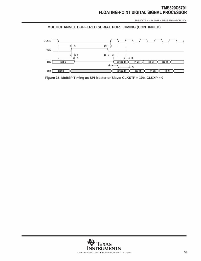
SPRS067F − MAY 1998 − REVISED MARCH 2004
57POST OFFICE BOX 1443 • HOUSTON, TEXAS 77251−1443
MULTICHANNEL BUFFERED SERIAL PORT TIMING (CONTINUED)
Bit 0 Bit(n-1) (n-2) (n-3) (n-4)
Bit 0 Bit(n-1) (n-2) (n-3) (n-4)5
4
387
6
21
CLKX
FSX
DX
DR
Figure 35. McBSP Timing as SPI Master or Slave: CLKSTP = 10b, CLKXP = 0

SPRS067F − MAY 1998 − REVISED MARCH 2004
58 POST OFFICE BOX 1443 • HOUSTON, TEXAS 77251−1443
MULTICHANNEL BUFFERED SERIAL PORT TIMING (CONTINUED)
timing requirements for McBSP as SPI master or slave: CLKSTP = 11b, CLKXP = 0 †‡ (see Figure 36)
NO.
C6701-120C6701-150C6701-167 UNITNO.
MASTER SLAVEUNIT
MIN MAX MIN MAX
4 tsu(DRV-CKXH) Setup time, DR valid before CLKX high 12 2 − 3P ns
5 th(CKXH-DRV) Hold time, DR valid after CLKX high 4 5 + 6P ns
† P = 1/CPU clock frequency in ns. For example, when running parts at 167 MHz, use P = 6 ns.‡ For all SPI slave modes, CLKG is programmed as 1/2 of the CPU clock by setting CLKSM = CLKGDV = 1.
switching characteristics for McBSP as SPI master or slave: CLKSTP = 11b, CLKXP = 0 †‡(see Figure 36)
NO. PARAMETER
C6701-120C6701-150C6701-167 UNITNO. PARAMETER
MASTER§ SLAVEUNIT
MIN MAX MIN MAX
1 th(CKXL-FXL) Hold time, FSX low after CLKX low¶ L − 4 L + 4 ns
2 td(FXL-CKXH) Delay time, FSX low to CLKX high# T − 4 T + 4 ns
3 td(CKXL-DXV) Delay time, CLKX low to DX valid −4 4 3P + 1 5P + 17 ns
6 tdis(CKXL-DXHZ)Disable time, DX high impedance following last data bit fromCLKX low
−2 4 3P + 4 5P + 17 ns
7 td(FXL-DXV) Delay time, FSX low to DX valid H − 2 H + 3 2P + 1 4P + 13 ns
† P = 1/CPU clock frequency in ns. For example, when running parts at 167 MHz, use P = 6 ns.‡ For all SPI slave modes, CLKG is programmed as 1/2 of the CPU clock by setting CLKSM = CLKGDV = 1.§ S = sample rate generator input clock = P if CLKSM = 1 (P = 1/CPU clock frequency)
= sample rate generator input clock = P_clks if CLKSM = 0 (P_clks = CLKS period)T = CLKX period = (1 + CLKGDV) * SH = CLKX high pulse width = (CLKGDV/2 + 1) * S if CLKGDV is even
= (CLKGDV + 1)/2 * S if CLKGDV is odd or zeroL = CLKX low pulse width = (CLKGDV/2) * S if CLKGDV is even
= (CLKGDV + 1)/2 * S if CLKGDV is odd or zero¶ FSRP = FSXP = 1. As a SPI master, FSX is inverted to provide active-low slave-enable output. As a slave, the active-low signal input on FSX
and FSR is inverted before being used internally.CLKXM = FSXM = 1, CLKRM = FSRM = 0 for master McBSPCLKXM = CLKRM = FSXM = FSRM = 0 for slave McBSP
# FSX should be low before the rising edge of clock to enable slave devices and then begin a SPI transfer at the rising edge of the master clock(CLKX).
Bit 0 Bit(n-1) (n-2) (n-3) (n-4)
Bit 0 Bit(n-1) (n-2) (n-3) (n-4)
4
376
21
CLKX
FSX
DX
DR
5
Figure 36. McBSP Timing as SPI Master or Slave: CLKSTP = 11b, CLKXP = 0

SPRS067F − MAY 1998 − REVISED MARCH 2004
59POST OFFICE BOX 1443 • HOUSTON, TEXAS 77251−1443
MULTICHANNEL BUFFERED SERIAL PORT TIMING (CONTINUED)
timing requirements for McBSP as SPI master or slave: CLKSTP = 10b, CLKXP = 1 †‡ (see Figure 37)
NO.
C6701-120C6701-150C6701-167 UNITNO.
MASTER SLAVEUNIT
MIN MAX MIN MAX
4 tsu(DRV-CKXH) Setup time, DR valid before CLKX high 12 2 − 3P ns
5 th(CKXH-DRV) Hold time, DR valid after CLKX high 4 5 + 6P ns
† P = 1/CPU clock frequency in ns. For example, when running parts at 167 MHz, use P = 6 ns.‡ For all SPI slave modes, CLKG is programmed as 1/2 of the CPU clock by setting CLKSM = CLKGDV = 1.
switching characteristics for McBSP as SPI master or slave: CLKSTP = 10b, CLKXP = 1 †‡(see Figure 37)
NO. PARAMETER
C6701-120C6701-150C6701-167 UNITNO. PARAMETER
MASTER§ SLAVEUNIT
MIN MAX MIN MAX
1 th(CKXH-FXL) Hold time, FSX low after CLKX high¶ T − 4 T + 4 ns
2 td(FXL-CKXL) Delay time, FSX low to CLKX low# H − 4 H + 4 ns
3 td(CKXL-DXV) Delay time, CLKX low to DX valid −4 4 3P + 1 5P + 17 ns
6 tdis(CKXH-DXHZ)Disable time, DX high impedance following last data bit fromCLKX high
H − 2 H + 3 ns
7 tdis(FXH-DXHZ)Disable time, DX high impedance following last data bit fromFSX high
P + 4 3P + 17 ns
8 td(FXL-DXV) Delay time, FSX low to DX valid 2P + 1 4P + 13 ns
† P = 1/CPU clock frequency in ns. For example, when running parts at 167 MHz, use P = 6 ns.‡ For all SPI slave modes, CLKG is programmed as 1/2 of the CPU clock by setting CLKSM = CLKGDV = 1.§ S = sample rate generator input clock = P if CLKSM = 1 (P = 1/CPU clock frequency)
= sample rate generator input clock = P_clks if CLKSM = 0 (P_clks = CLKS period)T = CLKX period = (1 + CLKGDV) * SH = CLKX high pulse width = (CLKGDV/2 + 1) * S if CLKGDV is even
= (CLKGDV + 1)/2 * S if CLKGDV is odd or zeroL = CLKX low pulse width = (CLKGDV/2) * S if CLKGDV is even
= (CLKGDV + 1)/2 * S if CLKGDV is odd or zero¶ FSRP = FSXP = 1. As a SPI master, FSX is inverted to provide active-low slave-enable output. As a slave, the active-low signal input on FSX
and FSR is inverted before being used internally.CLKXM = FSXM = 1, CLKRM = FSRM = 0 for master McBSPCLKXM = CLKRM = FSXM = FSRM = 0 for slave McBSP
# FSX should be low before the rising edge of clock to enable slave devices and then begin a SPI transfer at the rising edge of the master clock(CLKX).

SPRS067F − MAY 1998 − REVISED MARCH 2004
60 POST OFFICE BOX 1443 • HOUSTON, TEXAS 77251−1443
MULTICHANNEL BUFFERED SERIAL PORT TIMING (CONTINUED)
Bit 0 Bit(n-1) (n-2) (n-3) (n-4)
Bit 0 Bit(n-1) (n-2) (n-3) (n-4)54
387
6
21
CLKX
FSX
DX
DR
Figure 37. McBSP Timing as SPI Master or Slave: CLKSTP = 10b, CLKXP = 1

SPRS067F − MAY 1998 − REVISED MARCH 2004
61POST OFFICE BOX 1443 • HOUSTON, TEXAS 77251−1443
MULTICHANNEL BUFFERED SERIAL PORT TIMING (CONTINUED)
timing requirements for McBSP as SPI master or slave: CLKSTP = 11b, CLKXP = 1 †‡ (see Figure 38)
NO.
C6701-120C6701-150C6701-167 UNITNO.
MASTER SLAVEUNIT
MIN MAX MIN MAX
4 tsu(DRV-CKXL) Setup time, DR valid before CLKX low 12 2 − 3P ns
5 th(CKXL-DRV) Hold time, DR valid after CLKX low 4 5 + 6P ns
† P = 1/CPU clock frequency in ns. For example, when running parts at 167 MHz, use P = 6 ns.‡ For all SPI slave modes, CLKG is programmed as 1/2 of the CPU clock by setting CLKSM = CLKGDV = 1.
switching characteristics for McBSP as SPI master or slave: CLKSTP = 11b, CLKXP = 1 †‡(see Figure 38)
NO. PARAMETER
C6701-120C6701-150C6701-167 UNITNO. PARAMETER
MASTER§ SLAVEUNIT
MIN MAX MIN MAX
1 th(CKXH-FXL) Hold time, FSX low after CLKX high¶ H − 4 H + 4 ns
2 td(FXL-CKXL) Delay time, FSX low to CLKX low# T − 4 T + 4 ns
3 td(CKXH-DXV) Delay time, CLKX high to DX valid −4 4 3P + 1 5P + 17 ns
6 tdis(CKXH-DXHZ)Disable time, DX high impedance following last data bit fromCLKX high
−2 4 3P + 4 5P + 17 ns
7 td(FXL-DXV) Delay time, FSX low to DX valid L − 2 L + 3 2P + 1 4P + 13 ns
† P = 1/CPU clock frequency in ns. For example, when running parts at 167 MHz, use P = 6 ns.‡ For all SPI slave modes, CLKG is programmed as 1/2 of the CPU clock by setting CLKSM = CLKGDV = 1.§ S = sample rate generator input clock = P if CLKSM = 1 (P = 1/CPU clock frequency)
= sample rate generator input clock = P_clks if CLKSM = 0 (P_clks = CLKS period)T = CLKX period = (1 + CLKGDV) * SH = CLKX high pulse width = (CLKGDV/2 + 1) * S if CLKGDV is even
= (CLKGDV + 1)/2 * S if CLKGDV is odd or zeroL = CLKX low pulse width = (CLKGDV/2) * S if CLKGDV is even
= (CLKGDV + 1)/2 * S if CLKGDV is odd or zero¶ FSRP = FSXP = 1. As a SPI master, FSX is inverted to provide active-low slave-enable output. As a slave, the active-low signal input on FSX
and FSR is inverted before being used internally.CLKXM = FSXM = 1, CLKRM = FSRM = 0 for master McBSPCLKXM = CLKRM = FSXM = FSRM = 0 for slave McBSP
# FSX should be low before the rising edge of clock to enable slave devices and then begin a SPI transfer at the rising edge of the master clock(CLKX).

SPRS067F − MAY 1998 − REVISED MARCH 2004
62 POST OFFICE BOX 1443 • HOUSTON, TEXAS 77251−1443
MULTICHANNEL BUFFERED SERIAL PORT TIMING (CONTINUED)
Bit 0 Bit(n-1) (n-2) (n-3) (n-4)
Bit 0 Bit(n-1) (n-2) (n-3) (n-4)54
376
21
CLKX
FSX
DX
DR
Figure 38. McBSP Timing as SPI Master or Slave: CLKSTP = 11b, CLKXP = 1

SPRS067F − MAY 1998 − REVISED MARCH 2004
63POST OFFICE BOX 1443 • HOUSTON, TEXAS 77251−1443
DMAC, TIMER, POWER-DOWN TIMING
switching characteristics for DMAC outputs (see Figure 39)
NO. PARAMETER
C6701-120C6701-150C6701-167 UNIT
MIN MAX
1 td(CKO1H-DMACV) Delay time, CLKOUT1 high to DMAC valid 2 11 ns
11
CLKOUT1
DMAC[0:3]
Figure 39. DMAC Timing
timing requirements for timer inputs (see Figure 40) †
NO.
C6701-120C6701-150C6701-167 UNIT
MIN MAX
1 tw(TINPH) Pulse duration, TINP high 2P ns
† P = 1/CPU clock frequency in ns. For example, when running parts at 167 MHz, use P = 6 ns.
switching characteristics for timer outputs (see Figure 40)
NO. PARAMETER
C6701-120C6701-150C6701-167 UNIT
MIN MAX
2 td(CKO1H-TOUTV) Delay time, CLKOUT1 high to TOUT valid 1 10 ns
2
1
CLKOUT1
TINP
TOUT2
Figure 40. Timer Timing

SPRS067F − MAY 1998 − REVISED MARCH 2004
64 POST OFFICE BOX 1443 • HOUSTON, TEXAS 77251−1443
DMAC, TIMER, POWER-DOWN TIMING (CONTINUED)
switching characteristics for power-down outputs (see Figure 41)
NO. PARAMETER
C6701-120C6701-150C6701-167 UNIT
MIN MAX
1 td(CKO1H-PDV) Delay time, CLKOUT1 high to PD valid 1 9 ns
11
CLKOUT1
PD
Figure 41. Power-Down Timing

SPRS067F − MAY 1998 − REVISED MARCH 2004
65POST OFFICE BOX 1443 • HOUSTON, TEXAS 77251−1443
JTAG TEST-PORT TIMING
timing requirements for JTAG test port (see Figure 42)
NO.
C6701-120C6701-150C6701-167 UNIT
MIN MAX
1 tc(TCK) Cycle time, TCK 35 ns
3 tsu(TDIV-TCKH) Setup time, TDI/TMS/TRST valid before TCK high 10 ns
4 th(TCKH-TDIV) Hold time, TDI/TMS/TRST valid after TCK high 9 ns
switching characteristics for JTAG test port (see Figure 42)
NO. PARAMETER
C6701-120C6701-150C6701-167 UNIT
MIN MAX
2 td(TCKL-TDOV) Delay time, TCK low to TDO valid –3 12 ns
TCK
TDO
TDI/TMS/TRST
1
2
34
2
Figure 42. JTAG Test-Port Timing

SPRS067F − MAY 1998 − REVISED MARCH 2004
66 POST OFFICE BOX 1443 • HOUSTON, TEXAS 77251−1443
MECHANICAL DATA GJC (S-PBGA-N352) PLASTIC BALL GRID ARRAY
31,75 TYP
0,635
AF
AD
ABAC
Y
VW
AA
AE
RT
NP
LM
JK
G
EF
BC
A
D
H
U
252622
2320
19 2117151612
1314 1810
98
756
342
1
Seating Plane
11
4173506-2/D 07/99
24
SQ35,2034,80
SQ33,2032,80
21,00 NOM
See Note EHeat Slug
0,900,60
1,00 NOM
0,50 MIN
3,50 MAX
0,63
521,0
0 N
OM
1,27
0,15
1,27
M∅ 0,10
NOTES: A. All linear dimensions are in millimeters.B. This drawing is subject to change without notice.C. Thermally enhanced plastic package with heat slug (HSL).D. Flip chip application onlyE. Possible protrusion in this area, but within 3,50 max package height specificationF. Falls within JEDEC MO-151/BAR-2
thermal resistance characteristics (S-PBGA package)
NO °C/W Air Flow LFPM †
1 RΘJC Junction-to-case 0.74 N/A
2 RΘJA Junction-to-free air 11.31 0
3 RΘJA Junction-to-free air 9.60 100
4 RΘJA Junction-to-free air 8.34 250
5 RΘJA Junction-to-free air 7.30 500
† LFPM = Linear Feet Per Minute

SPRS067F − MAY 1998 − REVISED MARCH 2004
67POST OFFICE BOX 1443 • HOUSTON, TEXAS 77251−1443
REVISION HISTORY
This data sheet revision history highlights the technical changes made to the SPR067E device-specific datasheet to make it an SPRS067F revision.
Scope: Applicable updates to the C67x device family, specifically relating to the C6701 device, have been incor-porated.
PAGE(S)NO. ADDITIONS/CHANGES/DELETIONS
All Updated the title for literature number SPRU190 to:TMS320C6000 DSP Peripherals Overview Reference Guide
26 Added the power-down mode logic section and accompanying information.

PACKAGE OPTION ADDENDUM
www.ti.com 15-Apr-2017
Addendum-Page 1
PACKAGING INFORMATION
Orderable Device Status(1)
Package Type PackageDrawing
Pins PackageQty
Eco Plan(2)
Lead/Ball Finish(6)
MSL Peak Temp(3)
Op Temp (°C) Device Marking(4/5)
Samples
TMS320C6701GJC150 ACTIVE FCBGA GJC 352 24 TBD SNPB Level-4-220C-72 HR TMS320C6701@ 1998 TI320C6701GJC150
TMS320C6701GJCA120 ACTIVE FCBGA GJC 352 24 TBD SNPB Level-4-220C-72 HR TMS320C6701GJC@ 1998 TIA120320C6701
TMSC6701GJC16719V ACTIVE FCBGA GJC 352 24 TBD SNPB Level-4-220C-72 HR 0 to 0 TMS320C6701GJC@ 1998 TI320C6701
(1) The marketing status values are defined as follows:ACTIVE: Product device recommended for new designs.LIFEBUY: TI has announced that the device will be discontinued, and a lifetime-buy period is in effect.NRND: Not recommended for new designs. Device is in production to support existing customers, but TI does not recommend using this part in a new design.PREVIEW: Device has been announced but is not in production. Samples may or may not be available.OBSOLETE: TI has discontinued the production of the device.
(2) Eco Plan - The planned eco-friendly classification: Pb-Free (RoHS), Pb-Free (RoHS Exempt), or Green (RoHS & no Sb/Br) - please check http://www.ti.com/productcontent for the latest availabilityinformation and additional product content details.TBD: The Pb-Free/Green conversion plan has not been defined.Pb-Free (RoHS): TI's terms "Lead-Free" or "Pb-Free" mean semiconductor products that are compatible with the current RoHS requirements for all 6 substances, including the requirement thatlead not exceed 0.1% by weight in homogeneous materials. Where designed to be soldered at high temperatures, TI Pb-Free products are suitable for use in specified lead-free processes.Pb-Free (RoHS Exempt): This component has a RoHS exemption for either 1) lead-based flip-chip solder bumps used between the die and package, or 2) lead-based die adhesive used betweenthe die and leadframe. The component is otherwise considered Pb-Free (RoHS compatible) as defined above.Green (RoHS & no Sb/Br): TI defines "Green" to mean Pb-Free (RoHS compatible), and free of Bromine (Br) and Antimony (Sb) based flame retardants (Br or Sb do not exceed 0.1% by weightin homogeneous material)
(3) MSL, Peak Temp. - The Moisture Sensitivity Level rating according to the JEDEC industry standard classifications, and peak solder temperature.
(4) There may be additional marking, which relates to the logo, the lot trace code information, or the environmental category on the device.
(5) Multiple Device Markings will be inside parentheses. Only one Device Marking contained in parentheses and separated by a "~" will appear on a device. If a line is indented then it is a continuationof the previous line and the two combined represent the entire Device Marking for that device.

PACKAGE OPTION ADDENDUM
www.ti.com 15-Apr-2017
Addendum-Page 2
(6) Lead/Ball Finish - Orderable Devices may have multiple material finish options. Finish options are separated by a vertical ruled line. Lead/Ball Finish values may wrap to two lines if the finishvalue exceeds the maximum column width.
Important Information and Disclaimer:The information provided on this page represents TI's knowledge and belief as of the date that it is provided. TI bases its knowledge and belief on informationprovided by third parties, and makes no representation or warranty as to the accuracy of such information. Efforts are underway to better integrate information from third parties. TI has taken andcontinues to take reasonable steps to provide representative and accurate information but may not have conducted destructive testing or chemical analysis on incoming materials and chemicals.TI and TI suppliers consider certain information to be proprietary, and thus CAS numbers and other limited information may not be available for release.
In no event shall TI's liability arising out of such information exceed the total purchase price of the TI part(s) at issue in this document sold by TI to Customer on an annual basis.
OTHER QUALIFIED VERSIONS OF TMS320C6701 :
• Catalog: SM320C6701
• Enhanced Product: SM320C6701-EP
• Military: SMJ320C6701
NOTE: Qualified Version Definitions:
• Catalog - TI's standard catalog product
• Enhanced Product - Supports Defense, Aerospace and Medical Applications
• Military - QML certified for Military and Defense Applications

MECHANICAL DATA
MPBG067B – SEPTEMBER 1998 – REVISED JANUARY 2002
POST OFFICE BOX 655303 • DALLAS, TEXAS 75265
GJC (S-PBGA-N352) PLASTIC BALL GRID ARRAY
31,75 TYP
0,635
AF
AD
ABAC
Y
VW
AA
AE
RT
NP
LM
JK
G
EF
BC
A
D
H
U
252622
2320
19 2117151612
1314 1810
98
756
342
1
Seating Plane
11
4173506-2/E 11/01
24
SQ35,2034,80
SQ33,2032,80
21,00 NOM
See Note EHeat Slug
0,900,60
1,00 NOM
0,50 MIN
3,50 MAX
0,63
521,0
0 N
OM
1,27
0,15
1,27
M∅ 0,10
A1 CornerBottom View
NOTES: A. All linear dimensions are in millimeters.B. This drawing is subject to change without notice.C. Thermally enhanced plastic package with heat slug (HSL).D. Flip chip application onlyE. Possible protrusion in this area, but within 3,50 max package height specificationF. Falls within JEDEC MO-151/BAR-2

IMPORTANT NOTICE
Texas Instruments Incorporated (TI) reserves the right to make corrections, enhancements, improvements and other changes to itssemiconductor products and services per JESD46, latest issue, and to discontinue any product or service per JESD48, latest issue. Buyersshould obtain the latest relevant information before placing orders and should verify that such information is current and complete.TI’s published terms of sale for semiconductor products (http://www.ti.com/sc/docs/stdterms.htm) apply to the sale of packaged integratedcircuit products that TI has qualified and released to market. Additional terms may apply to the use or sale of other types of TI products andservices.Reproduction of significant portions of TI information in TI data sheets is permissible only if reproduction is without alteration and isaccompanied by all associated warranties, conditions, limitations, and notices. TI is not responsible or liable for such reproduceddocumentation. Information of third parties may be subject to additional restrictions. Resale of TI products or services with statementsdifferent from or beyond the parameters stated by TI for that product or service voids all express and any implied warranties for theassociated TI product or service and is an unfair and deceptive business practice. TI is not responsible or liable for any such statements.Buyers and others who are developing systems that incorporate TI products (collectively, “Designers”) understand and agree that Designersremain responsible for using their independent analysis, evaluation and judgment in designing their applications and that Designers havefull and exclusive responsibility to assure the safety of Designers' applications and compliance of their applications (and of all TI productsused in or for Designers’ applications) with all applicable regulations, laws and other applicable requirements. Designer represents that, withrespect to their applications, Designer has all the necessary expertise to create and implement safeguards that (1) anticipate dangerousconsequences of failures, (2) monitor failures and their consequences, and (3) lessen the likelihood of failures that might cause harm andtake appropriate actions. Designer agrees that prior to using or distributing any applications that include TI products, Designer willthoroughly test such applications and the functionality of such TI products as used in such applications.TI’s provision of technical, application or other design advice, quality characterization, reliability data or other services or information,including, but not limited to, reference designs and materials relating to evaluation modules, (collectively, “TI Resources”) are intended toassist designers who are developing applications that incorporate TI products; by downloading, accessing or using TI Resources in anyway, Designer (individually or, if Designer is acting on behalf of a company, Designer’s company) agrees to use any particular TI Resourcesolely for this purpose and subject to the terms of this Notice.TI’s provision of TI Resources does not expand or otherwise alter TI’s applicable published warranties or warranty disclaimers for TIproducts, and no additional obligations or liabilities arise from TI providing such TI Resources. TI reserves the right to make corrections,enhancements, improvements and other changes to its TI Resources. TI has not conducted any testing other than that specificallydescribed in the published documentation for a particular TI Resource.Designer is authorized to use, copy and modify any individual TI Resource only in connection with the development of applications thatinclude the TI product(s) identified in such TI Resource. NO OTHER LICENSE, EXPRESS OR IMPLIED, BY ESTOPPEL OR OTHERWISETO ANY OTHER TI INTELLECTUAL PROPERTY RIGHT, AND NO LICENSE TO ANY TECHNOLOGY OR INTELLECTUAL PROPERTYRIGHT OF TI OR ANY THIRD PARTY IS GRANTED HEREIN, including but not limited to any patent right, copyright, mask work right, orother intellectual property right relating to any combination, machine, or process in which TI products or services are used. Informationregarding or referencing third-party products or services does not constitute a license to use such products or services, or a warranty orendorsement thereof. Use of TI Resources may require a license from a third party under the patents or other intellectual property of thethird party, or a license from TI under the patents or other intellectual property of TI.TI RESOURCES ARE PROVIDED “AS IS” AND WITH ALL FAULTS. TI DISCLAIMS ALL OTHER WARRANTIES ORREPRESENTATIONS, EXPRESS OR IMPLIED, REGARDING RESOURCES OR USE THEREOF, INCLUDING BUT NOT LIMITED TOACCURACY OR COMPLETENESS, TITLE, ANY EPIDEMIC FAILURE WARRANTY AND ANY IMPLIED WARRANTIES OFMERCHANTABILITY, FITNESS FOR A PARTICULAR PURPOSE, AND NON-INFRINGEMENT OF ANY THIRD PARTY INTELLECTUALPROPERTY RIGHTS. TI SHALL NOT BE LIABLE FOR AND SHALL NOT DEFEND OR INDEMNIFY DESIGNER AGAINST ANY CLAIM,INCLUDING BUT NOT LIMITED TO ANY INFRINGEMENT CLAIM THAT RELATES TO OR IS BASED ON ANY COMBINATION OFPRODUCTS EVEN IF DESCRIBED IN TI RESOURCES OR OTHERWISE. IN NO EVENT SHALL TI BE LIABLE FOR ANY ACTUAL,DIRECT, SPECIAL, COLLATERAL, INDIRECT, PUNITIVE, INCIDENTAL, CONSEQUENTIAL OR EXEMPLARY DAMAGES INCONNECTION WITH OR ARISING OUT OF TI RESOURCES OR USE THEREOF, AND REGARDLESS OF WHETHER TI HAS BEENADVISED OF THE POSSIBILITY OF SUCH DAMAGES.Unless TI has explicitly designated an individual product as meeting the requirements of a particular industry standard (e.g., ISO/TS 16949and ISO 26262), TI is not responsible for any failure to meet such industry standard requirements.Where TI specifically promotes products as facilitating functional safety or as compliant with industry functional safety standards, suchproducts are intended to help enable customers to design and create their own applications that meet applicable functional safety standardsand requirements. Using products in an application does not by itself establish any safety features in the application. Designers mustensure compliance with safety-related requirements and standards applicable to their applications. Designer may not use any TI products inlife-critical medical equipment unless authorized officers of the parties have executed a special contract specifically governing such use.Life-critical medical equipment is medical equipment where failure of such equipment would cause serious bodily injury or death (e.g., lifesupport, pacemakers, defibrillators, heart pumps, neurostimulators, and implantables). Such equipment includes, without limitation, allmedical devices identified by the U.S. Food and Drug Administration as Class III devices and equivalent classifications outside the U.S.TI may expressly designate certain products as completing a particular qualification (e.g., Q100, Military Grade, or Enhanced Product).Designers agree that it has the necessary expertise to select the product with the appropriate qualification designation for their applicationsand that proper product selection is at Designers’ own risk. Designers are solely responsible for compliance with all legal and regulatoryrequirements in connection with such selection.Designer will fully indemnify TI and its representatives against any damages, costs, losses, and/or liabilities arising out of Designer’s non-compliance with the terms and provisions of this Notice.
Mailing Address: Texas Instruments, Post Office Box 655303, Dallas, Texas 75265Copyright © 2017, Texas Instruments Incorporated
Related Documents