TLC193, TLC393 DUAL MICROPOWER LinCMOS VOLTAGE COMPARATOR SLCS115E - DECEMBER 1986 - REVISED JULY 2003 1 POST OFFICE BOX 655303 • DALLAS, TEXAS 75265 POST OFFICE BOX 1443 • HOUSTON, TEXAS 77251-1443 D Very Low Power . . . 110 µW Typ at 5 V D Fast Response Time . . . t PLH = 2.5 µs Typ With 5-mV Overdrive D Single Supply Operation: TLC393C . . . 3 V to 16 V TLC393I . . . 3 V to 16 V TLC393Q . . . 4 V to 16 V TLC393M . . . 4 V to 16 V TLC193M . . . 4 V to 16 V D On-Chip ESD Protection description The TLC193 and TLC393 consist of dual independent micropower voltage comparators designed to operate from a single supply. They are functionally similar to the LM393 but uses one-twentieth the power for similar response times. The open-drain MOS output stage interfaces to a variety of loads and supplies. For a similar device with a push-pull output configuration (see the TLC3702 data sheet). Texas Instruments LinCMOS process offers superior analog performance to standard CMOS processes. Along with the standard CMOS advantages of low power without sacrificing speed, high input impedance, and low bias currents, the LinCMOS process offers ex- tremely stable input offset voltages, even with differential input stresses of several volts. This characteristic makes it possible to build reliable CMOS comparators. The TLC393C is characterized for operation over the commercial temperature range of T A = 0°C to 70°C. The TLC393I is characterized for operation over the extended industrial temperature range of T A = -40°C to 85°C. The TLC393Q is characterized for operation over the full automotive temperature range of T A = -40°C to 125°C. The TLC193M and TLC393M are characterized for operation over the full military temperature range of T A = -55°C to 125°C. Please be aware that an important notice concerning availability, standard warranty, and use in critical applications of Texas Instruments semiconductor products and disclaimers thereto appears at the end of this data sheet. Copyright 1986-2003, Texas Instruments Incorporated PRODUCTION DATA information is current as of publication date. Products conform to specifications per the terms of Texas Instruments standard warranty. Production processing does not necessarily include testing of all parameters. 3 2 1 20 19 9 10 11 12 13 4 5 6 7 8 18 17 16 15 14 NC 2OUT NC 2IN- NC NC 1IN- NC 1IN+ NC NC 1OUT NC 2IN+ NC V NC GND NC NC DD D, JG, P, OR PW PACKAGE (TOP VIEW) 1 2 3 4 8 7 6 5 1OUT 1IN- 1IN+ GND V DD 2OUT 2IN- 2IN+ NC - No internal connection OUT symbol (each comparator) IN+ IN- FK PACKAGE (TOP VIEW) LinCMOS is a trademark of Texas Instruments Incorporated. All other trademarks are the property of their respective owners.

Welcome message from author
This document is posted to help you gain knowledge. Please leave a comment to let me know what you think about it! Share it to your friends and learn new things together.
Transcript

SLCS115E − DECEMBER 1986 − REVISED JULY 2003
1POST OFFICE BOX 655303 • DALLAS, TEXAS 75265POST OFFICE BOX 1443 • HOUSTON, TEXAS 77251−1443
Very Low Power . . . 110 µW Typ at 5 V
Fast Response Time . . . tPLH = 2.5 µs TypWith 5-mV Overdrive
Single Supply Operation:TLC393C . . . 3 V to 16 VTLC393I . . . 3 V to 16 VTLC393Q . . . 4 V to 16 VTLC393M . . . 4 V to 16 VTLC193M . . . 4 V to 16 V
On-Chip ESD Protection
description
The TLC193 and TLC393 consist of dualindependent micropower voltage comparatorsdesigned to operate from a single supply. Theyare functionally similar to the LM393 but usesone-twentieth the power for similar responsetimes. The open-drain MOS output stageinterfaces to a variety of loads and supplies. Fora similar device with a push-pull outputconfiguration (see the TLC3702 data sheet).
Texas Instruments LinCMOS process offerssuperior analog performance to standard CMOSprocesses. Along with the standard CMOSadvantages of low power without sacrificingspeed, high input impedance, and low biascurrents, the LinCMOS process offers ex-tremely stable input offset voltages, even withdifferential input stresses of several volts. Thischaracteristic makes it possible to build reliableCMOS comparators.
The TLC393C is characterized for operation over the commercial temperature range of TA = 0°C to 70°C. TheTLC393I is characterized for operation over the extended industrial temperature range of TA = −40°C to 85°C.The TLC393Q is characterized for operation over the full automotive temperature range of TA = −40°C to 125°C.The TLC193M and TLC393M are characterized for operation over the full military temperature range of TA = −55°C to 125°C.
Please be aware that an important notice concerning availability, standard warranty, and use in critical applications ofTexas Instruments semiconductor products and disclaimers thereto appears at the end of this data sheet.
Copyright 1986-2003, Texas Instruments Incorporated !" #!$% &"'&! #" #" (" " ") !"&& *+' &! # ", &" " "%+ %!&"", %% #""'
3 2 1 20 19
9 10 11 12 13
4
5
6
7
8
18
17
16
15
14
NC2OUTNC2IN−NC
NC1IN−
NC1IN+
NC
NC
1OU
TN
C
2IN
+N
CV N
C
GN
DN
C
NC
DD
D, JG, P, OR PW PACKAGE(TOP VIEW)
1
2
3
4
8
7
6
5
1OUT1IN−1IN+GND
VDD2OUT2IN−2IN+
NC − No internal connection
OUT
symbol (each comparator)
IN+
IN−
FK PACKAGE(TOP VIEW)
LinCMOS is a trademark of Texas Instruments Incorporated. All other trademarks are the property of their respective owners.

SLCS115D − DECEMBER 1986 − REVISED JULY 2003
2 POST OFFICE BOX 655303 • DALLAS, TEXAS 75265POST OFFICE BOX 1443 • HOUSTON, TEXAS 77251−1443
AVAILABLE OPTIONS
V maxPACKAGES
TAVIOmaxat 25°C SMALL OUTLINE
(D)CHIP CARRIER
(FK)CERAMIC DIP
(JG)PLASTIC DIP
(P)TSSOP
(PW)
0°C to 70°C 5 mV TLC393CD — — TLC393CP TLC393CPWLE
− 40°C to 85°C 5 mV TLC393ID — — TLC393IP TLC393IPWLE
− 40°C to 125°C 5 mV TLC393QD — — — —
− 55°C to 125°C 5 mV TLC393MD TLC193MFK TLC193MJG TLC393MP —
The D package is available taped and reeled. Add the suffix R to the device type (e.g., TLC393CDR).
schematicOUT
OPEN-DRAIN CMOS OUTPUT
absolute maximum ratings over operating free-air temperature range (unless otherwise noted)†
Supply voltage range, VDD (see Note 1) − 0.3 V to 18 V. . . . . . . . . . . . . . . . . . . . . . . . . . . . . . . . . . . . . . . . . . . . . Differential input voltage, VID (see Note 2) ±18 V. . . . . . . . . . . . . . . . . . . . . . . . . . . . . . . . . . . . . . . . . . . . . . . . . . . Input voltage range, VI − 0.3 V to VDD. . . . . . . . . . . . . . . . . . . . . . . . . . . . . . . . . . . . . . . . . . . . . . . . . . . . . . . . . . . . . Output voltage range, VO − 0.3 V to 16 V. . . . . . . . . . . . . . . . . . . . . . . . . . . . . . . . . . . . . . . . . . . . . . . . . . . . . . . . . . Input current, II ±5 mA. . . . . . . . . . . . . . . . . . . . . . . . . . . . . . . . . . . . . . . . . . . . . . . . . . . . . . . . . . . . . . . . . . . . . . . . . . Output current, IO (each output) 20 mA. . . . . . . . . . . . . . . . . . . . . . . . . . . . . . . . . . . . . . . . . . . . . . . . . . . . . . . . . . . Total supply current into VDD 40 mA. . . . . . . . . . . . . . . . . . . . . . . . . . . . . . . . . . . . . . . . . . . . . . . . . . . . . . . . . . . . . . Total current out of GND 40 mA. . . . . . . . . . . . . . . . . . . . . . . . . . . . . . . . . . . . . . . . . . . . . . . . . . . . . . . . . . . . . . . . . . Continuous total power dissipation See Dissipation Rating Table. . . . . . . . . . . . . . . . . . . . . . . . . . . . . . . . . . . . . Operating free-air temperature range: TLC393C 0°C to 70°C. . . . . . . . . . . . . . . . . . . . . . . . . . . . . . . . . . . . . . .
TLC393I − 40°C to 85°C. . . . . . . . . . . . . . . . . . . . . . . . . . . . . . . . . . . . . . TLC393Q − 40°C to 125°C. . . . . . . . . . . . . . . . . . . . . . . . . . . . . . . . . . . TLC393M − 55°C to 125°C. . . . . . . . . . . . . . . . . . . . . . . . . . . . . . . . . . . TLC193M − 55°C to 125°C. . . . . . . . . . . . . . . . . . . . . . . . . . . . . . . . . . .
Storage temperature range − 65°C to 150°C. . . . . . . . . . . . . . . . . . . . . . . . . . . . . . . . . . . . . . . . . . . . . . . . . . . . . . . Case temperature for 60 seconds: FK package 260°C. . . . . . . . . . . . . . . . . . . . . . . . . . . . . . . . . . . . . . . . . . . . . . Lead temperature 1,6 mm (1/16 inch) from case for 10 seconds: D or P package 260°C. . . . . . . . . . . . . . . . . Lead temperature 1,6 mm (1/16 inch) from case for 60 seconds: JG package 300°C. . . . . . . . . . . . . . . . . . . .
† Stresses beyond those listed under “absolute maximum ratings” may cause permanent damage to the device. These are stress ratings only, andfunctional operation of the device at these or any other conditions beyond those indicated under “recommended operating conditions” is notimplied. Exposure to absolute-maximum-rated conditions for extended periods may affect device reliability.
NOTES: 1. All voltage values, except differential voltages, are with respect to network ground.2. Differential voltages are at IN+ with respect to IN−.
DISSIPATION RATING TABLE
PACKAGETA ≤ 25°C
POWER RATINGDERATING FACTORABOVE TA = 25°C
TA = 70°CPOWER RATING
TA = 85°CPOWER RATING
TA = 125°CPOWER RATING
D 725 mW 5.8 mW/°C 464 mW 377 mW 145 mW
FK 1375 mW 11.0 mW/°C 880 mW 715 mW 275 mW
JG 1050 mW 8.4 mW/°C 672 mW 546 mW 210 mW
P 1000 mW 8.0 mW/°C 640 mW 520 mW —
PW 525 mW 4.2 mW/°C 336 mW 273 mW —

SLCS115E − DECEMBER 1986 − REVISED JULY 2003
3POST OFFICE BOX 655303 • DALLAS, TEXAS 75265POST OFFICE BOX 1443 • HOUSTON, TEXAS 77251−1443
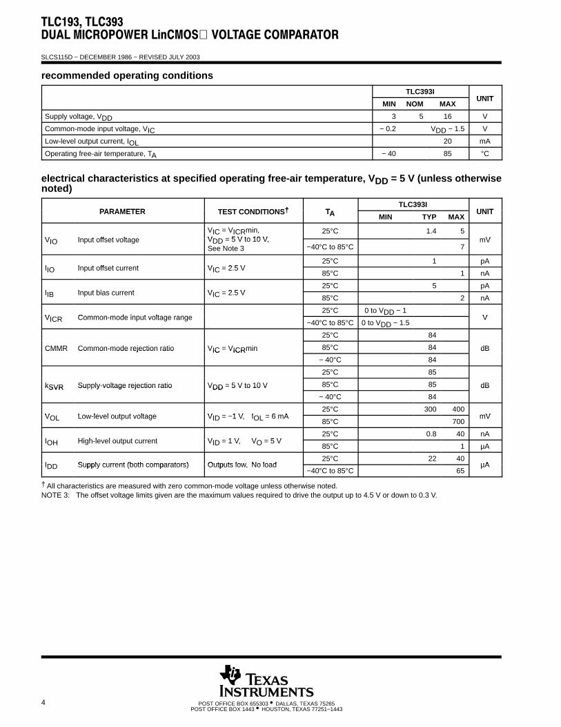
recommended operating conditions
TLC393CUNIT
MIN NOM MAXUNIT
Supply voltage, VDD 3 5 16 V
Common-mode input voltage, VIC −0.2 VDD − 1.5 V
Low-level output current, IOL 20 mA
Operating free-air temperature, TA 0 70 °C
electrical characteristics at specified operating free-air temperature, VDD = 5 V (unless otherwisenoted)
PARAMETER TEST CONDITIONS† TTLC393C
UNITPARAMETER TEST CONDITIONS† TA MIN TYP MAXUNIT
V Inp t offset oltageVIC = VICRmin,VDD 5 V to 10 V
25°C 1.4 5mVVIO Input offset voltage VDD = 5 V to 10 V,
See Note 3 0°C to 70°C 6.5mV
I Inp t offset c rrent V 2 5 V25°C 1 pA
IIO Input offset current VIC = 2.5 V70°C 0.3 nA
I Inp t bias c rrent V 2 5 V25°C 5 pA
IIB Input bias current VIC = 2.5 V70°C 0.6 nA
V Common mode inp t oltage range25°C 0 to VDD − 1
VVICR Common-mode input voltage range0°C to 70°C 0 to VDD − 1.5
V
25°C 84
CMMR Common-mode rejection ratio VIC = VICRmin 70°C 84 dBCMMR Common mode rejection ratio VIC VICRmin
0°C 84
dB
25°C 85
kSVR Supply-voltage rejection ratio VDD = 5 V to 10 V 70°C 85 dBkSVR Su ly voltage rejection ratio VDD 5 V to 10 V
0°C 85
dB
V Lo le el o tp t oltage V 1 V I 6 mA25°C 300 400
mVVOL Low-level output voltage VID = −1 V, IOL = 6 mA70°C 650
mV
I High le el o tp t c rrent V 1 V V 5 V25°C 0.8 40 nA
IOH High-level output current VID = 1 V, VO = 5 V70°C 1 µA
IDD Supply current (both comparators) Outputs low No load25°C 22 40
µAIDD Supply current (both comparators) Outputs low, No load0°C to 70°C 50
µA
† All characteristics are measured with zero common-mode voltage unless otherwise noted.NOTE 3: The offset voltage limits given are the maximum values required to drive the output up to 4.5 V or down to 0.3 V.
SLCS115D − DECEMBER 1986 − REVISED JULY 2003
4 POST OFFICE BOX 655303 • DALLAS, TEXAS 75265POST OFFICE BOX 1443 • HOUSTON, TEXAS 77251−1443
recommended operating conditions
TLC393IUNIT
MIN NOM MAXUNIT
Supply voltage, VDD 3 5 16 V
Common-mode input voltage, VIC − 0.2 VDD − 1.5 V
Low-level output current, IOL 20 mA
Operating free-air temperature, TA − 40 85 °C
electrical characteristics at specified operating free-air temperature, VDD = 5 V (unless otherwisenoted)
PARAMETER TEST CONDITIONS† TTLC393I
UNITPARAMETER TEST CONDITIONS† TA MIN TYP MAXUNIT
V Inp t offset oltageVIC = VICRmin,VDD 5 V to 10 V
25°C 1.4 5mVVIO Input offset voltage VDD = 5 V to 10 V,
See Note 3 −40°C to 85°C 7mV
I Inp t offset c rrent V 2 5 V25°C 1 pA
IIO Input offset current VIC = 2.5 V85°C 1 nA
I Inp t bias c rrent V 2 5 V25°C 5 pA
IIB Input bias current VIC = 2.5 V85°C 2 nA
V Common mode inp t oltage range25°C 0 to VDD − 1
VVICR Common-mode input voltage range−40°C to 85°C 0 to VDD − 1.5
V
25°C 84
CMMR Common-mode rejection ratio VIC = VICRmin 85°C 84 dBCMMR Common mode rejection ratio VIC VICRmin
− 40°C 84
dB
25°C 85
kSVR Supply-voltage rejection ratio VDD = 5 V to 10 V 85°C 85 dBkSVR Su ly voltage rejection ratio VDD 5 V to 10 V
− 40°C 84
dB
V Lo le el o tp t oltage V 1 V I 6 mA25°C 300 400
mVVOL Low-level output voltage VID = −1 V, IOL = 6 mA85°C 700
mV
I High le el o tp t c rrent V 1 V V 5 V25°C 0.8 40 nA
IOH High-level output current VID = 1 V, VO = 5 V85°C 1 µA
IDD Supply current (both comparators) Outputs low No load25°C 22 40
µAIDD Supply current (both comparators) Outputs low, No load−40°C to 85°C 65
µA
† All characteristics are measured with zero common-mode voltage unless otherwise noted.NOTE 3: The offset voltage limits given are the maximum values required to drive the output up to 4.5 V or down to 0.3 V.

SLCS115E − DECEMBER 1986 − REVISED JULY 2003
5POST OFFICE BOX 655303 • DALLAS, TEXAS 75265POST OFFICE BOX 1443 • HOUSTON, TEXAS 77251−1443
recommended operating conditions
TLC393QUNIT
MIN NOM MAXUNIT
Supply voltage, VDD 4 5 16 V
Common-mode input voltage, VIC 0 VDD − 1.5 V
Low-level output current, IOL 20 mA
Operating free-air temperature, TA −40 125 °C
electrical characteristics at specified operating free-air temperature, VDD = 5 V (unless otherwisenoted)
PARAMETER TEST CONDITIONS† TTLC393Q
UNITPARAMETER TEST CONDITIONS† TA MIN TYP MAXUNIT
V Inp t offset oltageVIC = VICRmin,VDD 5 V to 10 V
25°C 1.4 5mVVIO Input offset voltage VDD = 5 V to 10 V,
See Note 4 −40°C to 125°C 10mV
I Inp t offset c rrent V 2 5 V25°C 1 pA
IIO Input offset current VIC = 2.5 V125°C 15 nA
I Inp t bias c rrent V 2 5 V25°C 5 pA
IIB Input bias current VIC = 2.5 V125°C 30 nA
V Common mode inp t oltage range25°C 0 to VDD − 1
VVICR Common-mode input voltage range−40°C to 125°C 0 to VDD − 1.5
V
25°C 84
CMMR Common-mode rejection ratio VIC = VICRmin 125°C 84 dBCMMR Common mode rejection ratio VIC VICRmin
−40°C 84
dB
25°C 85
kSVR Supply-voltage rejection ratio VDD = 5 V to 10 V 125°C 84 dBkSVR Su ly voltage rejection ratio VDD 5 V to 10 V
−40°C 84
dB
V Lo le el o tp t oltage V 1 V I 6 mA25°C 300 400
mVVOL Low-level output voltage VID = −1 V, IOL = 6 mA125°C 800
mV
I High le el o tp t c rrent V 1 V V 5 V25°C 0.8 40 nA
IOH High-level output current VID = 1 V, VO = 5 V125°C 1 µA
IDD Supply current (both comparators) Outputs low No load25°C 22 40
µAIDD Supply current (both comparators) Outputs low, No load−40°C to 125°C 90
µA
† All characteristics are measured with zero common-mode voltage unless otherwise noted.NOTE 4: The offset voltage limits given are the maximum values required to drive the output up to 4.5 V or down to 0.3 V (with a 2.5-kΩ load to
VDD).

SLCS115D − DECEMBER 1986 − REVISED JULY 2003
6 POST OFFICE BOX 655303 • DALLAS, TEXAS 75265POST OFFICE BOX 1443 • HOUSTON, TEXAS 77251−1443
recommended operating conditions
TLC193M, TLC393MUNIT
MIN NOM MAXUNIT
Supply voltage, VDD 4 5 16 V
Common-mode input voltage, VIC 0 VDD − 1.5 V
Low-level output current, IOL 20 mA
Operating free-air temperature, TA −55 125 °C
electrical characteristics at specified operating free-air temperature, VDD = 5 V (unless otherwisenoted)
PARAMETER TEST CONDITIONS† TTLC193M, TLC393M
UNITPARAMETER TEST CONDITIONS† TA MIN TYP MAXUNIT
V Inp t offset oltageVIC = VICRmin,VDD 5 V to 10 V
25°C 1.4 5mVVIO Input offset voltage VDD = 5 V to 10 V,
See Note 4 −55°C to 125°C 10mV
I Inp t offset c rrent V 2 5 V25°C 1 pA
IIO Input offset current VIC = 2.5 V125°C 15 nA
I Inp t bias c rrent V 2 5 V25°C 5 pA
IIB Input bias current VIC = 2.5 V125°C 30 nA
V Common mode inp t oltage range25°C 0 to VDD − 1
VVICR Common-mode input voltage range−55°C to 125°C 0 to VDD − 1.5
V
25°C 84
CMMR Common-mode rejection ratio VIC = VICRmin 125°C 84 dBCMMR Common mode rejection ratio VIC VICRmin
−55°C 84
dB
25°C 85
kSVR Supply-voltage rejection ratio VDD = 5 V to 10 V 125°C 84 dBkSVR Su ly voltage rejection ratio VDD 5 V to 10 V
−55°C 84
dB
V Lo le el o tp t oltage V 1 V I 6 mA25°C 300 400
mVVOL Low-level output voltage VID = −1 V, IOL = 6 mA125°C 800
mV
I High le el o tp t c rrent V 1 V V 5 V25°C 0.8 40 nA
IOH High-level output current VID = 1 V, VO = 5 V125°C 1 µA
IDD Supply current (both comparators) Outputs low No load25°C 22 40
µAIDD Supply current (both comparators) Outputs low, No load−55°C to 125°C 90
µA
† All characteristics are measured with zero common-mode voltage unless otherwise noted.NOTE 4: The offset voltage limits given are the maximum values required to drive the output up to 4.5 V or down to 0.3 V (with a 2.5-kΩ load to
VDD).

SLCS115E − DECEMBER 1986 − REVISED JULY 2003
7POST OFFICE BOX 655303 • DALLAS, TEXAS 75265POST OFFICE BOX 1443 • HOUSTON, TEXAS 77251−1443
switching characteristics, VDD = 5 V, TA = 25°C (see Figure 3)
PARAMETER TEST CONDITIONS
TLC393C, TLC393ITLC393Q, TLC193M,
TLC393M UNIT
MIN TYP MAX
Overdrive = 2 mV 4.5
f 10 kHOverdrive = 5 mV 2.5
tPLH Propagation delay time, low-to-high-level outputf = 10 kHz,CL = 15 pF
Overdrive = 10 mV 1.7 µstPLH Pro agation delay time, low to high level out ut CL = 15 pFOverdrive = 20 mV 1.2
µs
Overdrive = 40 mV 1.1
VI = 1.4-V step at IN+ 1.1
Overdrive = 2 mV 3.6
f 10 kHOverdrive = 5 mV 2.1
tPHL Propagation delay time, high-to-low-level outputf = 10 kHz,CL = 15 pF
Overdrive = 10 mV 1.3 µstPHL Pro agation delay time, high to low level out ut CL = 15 pFOverdrive = 20 mV 0.85
µs
Overdrive = 40 mV 0.55
VI = 1.4-V step at IN+ 0.10
tf Fall time, outputf = 10 kHz,CL = 15 pF
Overdrive = 50 mV 22 ns
PARAMETER MEASUREMENT INFORMATION
The TLC393 contains a digital output stage which, if held in the linear region of the transfer curve, can causedamage to the device. Conventional operational amplifier/comparator testing incorporates the use of a servoloop that is designed to force the device output to a level within this linear region. Since the servo-loop methodof testing cannot be used, the following alternatives for testing parameters such as input offset voltage,common-mode rejection ratio, etc., are suggested.
To verify that the input offset voltage falls within the limits specified, the limit value is applied to the input as shownin Figure 1(a). With the noninverting input positive with respect to the inverting input, the output should be high.With the input polarity reversed, the output should be low.
A similar test can be made to verify the input offset voltage at the common-mode extremes. The supply voltagescan be slewed as shown in Figure 1(b) for the VICR test, rather than changing the input voltages, to providegreater accuracy.
+
−
5 V
Applied VIO Limit VO
+
−
1 V
Applied VIO Limit VO
− 4 V
(a) VIO WITH VIC = 0 V (b) VIO WITH VIC = 4 V
5.1 kΩ 5.1 kΩ
Figure 1. Method for Verifying That Input Offset Voltage Is Within Specified Limits

SLCS115D − DECEMBER 1986 − REVISED JULY 2003
8 POST OFFICE BOX 655303 • DALLAS, TEXAS 75265POST OFFICE BOX 1443 • HOUSTON, TEXAS 77251−1443
PARAMETER MEASUREMENT INFORMATION
A close approximation of the input offset voltage can be obtained by using a binary search method to vary thedifferential input voltage while monitoring the output state. When the applied input voltage differential is equal,but opposite in polarity, to the input offset voltage, the output changes states.
Figure 2 illustrates a practical circuit for direct dc measurement of input offset voltage that does not bias thecomparator in the linear region. The circuit consists of a switching-mode servo loop in which U1A generatesa triangular waveform of approximately 20-mV amplitude. U1B acts as a buffer, with C2 and R4 removing anyresidual dc offset. The signal is then applied to the inverting input of the comparator under test, while thenoninverting input is driven by the output of the integrator formed by U1C through the voltage divider formedby R9 and R10. The loop reaches a stable operating point when the output of the comparator under test hasa duty cycle of exactly 50%, which can only occur when the incoming triangle wave is sliced symmetrically orwhen the voltage at the noninverting input exactly equals the input offset voltage.
The voltage divider formed by R9 and R10 provides an increase in input offset voltage by a factor of 100 tomake measurement easier. The values of R5, R8, R9, and R10 can significantly influence the accuracy of thereading; therefore, it is suggested that their tolerance level be 1% or lower.
Measuring the extremely low values of input current requires isolation from all other sources of leakage currentand compensation for the leakage of the test socket and board. With a good picoammeter, the socket and boardleakage can be measured with no device in the socket. Subsequently, this open-socket leakage value can besubtracted from the measurement obtained with a device in the socket to obtain the actual input current of thedevice.
−
+
DUT
VDD
+
−
−
+
−
+
C21 µF
R447 kΩ
R51.8 kΩ, 1%
C30.68 µF
U1C1/4 TLC274CN
U1B1/4 TLC274CN
U1A1/4 TLC274CN
R71 MΩ
R81.8 kΩ, 1%
R910 kΩ, 1%
R1240 kΩ
R210 kΩ
C10.1 µF
R3100 kΩ
C40.1 µF
Integrator
R10100 Ω, 1%
Buffer
TriangleGenerator
VIO(X100)
R65.1 kΩ
Figure 2. Circuit for Input Offset Voltage Measurement

SLCS115E − DECEMBER 1986 − REVISED JULY 2003
9POST OFFICE BOX 655303 • DALLAS, TEXAS 75265POST OFFICE BOX 1443 • HOUSTON, TEXAS 77251−1443
PARAMETER MEASUREMENT INFORMATION
Propagation delay time is defined as the interval between the application of an input step function and the instantwhen the output reaches 50% of its maximum value. Propagation delay time, low-to-high-level output, ismeasured from the leading edge of the input pulse, while propagation delay time, high-to-low-level output, ismeasured from the trailing edge of the input pulse. Propagation delay time measurement at low input signallevels can be greatly affected by the input offset voltage. The offset voltage should be balanced by theadjustment at the inverting input (as shown in Figure 3) so that the circuit is just at the transition point. Then alow signal, for example, 105 mV or 5 mV overdrive, causes the output to change state.
DUT
VDD
CL(see Note A)
PulseGenerator
10 Ω10 Turn
1 V
− 1 V1 kΩ
50 Ω
1 µF
0.1 µF
TEST CIRCUIT
100 mVInput
Overdrive
50%
tPLH
100 mVInput
Overdrive
90%
50%
10%
tf
tPHL
Low-to-High-Level Output
High-to-Low-Level Output
VOLTAGE WAVEFORMS
5.1 kΩ
Input Offset VoltageCompensationAdjustment
90%
tr
10%
NOTE A: CL includes probe and jig capacitance.
Figure 3. Propagation Delay, Rise Time, and Fall Time Circuit and Voltage Waveforms

SLCS115D − DECEMBER 1986 − REVISED JULY 2003
10 POST OFFICE BOX 655303 • DALLAS, TEXAS 75265POST OFFICE BOX 1443 • HOUSTON, TEXAS 77251−1443
TYPICAL CHARACTERISTICS
Table of Graphs
FIGURE
VIO Input offset voltage Distribution 4
IIB Input bias current vs Free-air temperature 5
CMRR Common-mode rejection ratio vs Free-air temperature 6
kSVR Supply-voltage rejection ratio vs Free-air temperature 7
V Lo le el o tp t oltagevs Low-level output current 8
VOL Low-level output voltagevs Low level out ut currentvs Free-air temperature
89
I Lo le el o tp t c rrentvs High-level output voltage 10
IOH Low-level output currentvs High level out ut voltagevs Free-air temperature
1011
I S ppl c rrentvs Supply voltage 12
IDD Supply currentvs Su ly voltagevs Free-air temperature
1213
tPLH Low-to-high level output propagation delay time vs Supply voltage 14
tPHL High-to-low level output propagation delay time vs Supply voltage 15
Low-to-high-level output response Low-to-high level output propagation delay time 16
High-to-low level output response High-to-low level output propagation delay time 17
tf Fall time vs Supply voltage 18
Figure 4
ÉÉÉÉÉÉÇÇ
ÇÇÇÇÇÇÇ
ÉÉÉÉÉÉÉÉÉÉ
ÇÇÇÇÇÇÇÇÇÇÇÇÇÇÇÇÇÇÇÇÇÇ
ÇÇÇÇÇÇÇÇÇÇÇÇÇÇÇÇÇÇÇÇ
ÉÉÉÉÉÉÉÉÉ
ÇÇÇÇÉÉÉÉÉÇ
ÇÇÇÇÇÇÇÇ
ÉÉÉÉÉÉÉÉÉÉ
ÉÉÉÉÉÉÉÇ
Nu
mb
er o
f U
nit
s
VDD = 5 VVIC = 2.5 VTA = 25°C
−5 −4 −3 −2 −1 0 1 2 3 4 5
VIO − Input Offset Voltage − mV
DISTRIBUTION OF INPUTOFFSET VOLTAGE†
100
90
80
70
60
50
40
30
20
10
0Ç
ÉÉÉÉÉÉÉÉÉÉÉÉ
Figure 5
I
TA − Free-Air Temperature − °C
IB −
Inp
ut
Bia
s C
urr
ent
− n
A
25 50 75 100 125
10
1
0.1
0.01
0.001
INPUT BIAS CURRENTvs
FREE-AIR TEMPERATURE†
VDD = 5 VVIC = 2.5 V
† Data at high and low temperatures are applicable only within the rated operating free-air temperature ranges of the various devices.

SLCS115E − DECEMBER 1986 − REVISED JULY 2003
11POST OFFICE BOX 655303 • DALLAS, TEXAS 75265POST OFFICE BOX 1443 • HOUSTON, TEXAS 77251−1443
TYPICAL CHARACTERISTICS†
Figure 6
CM
RR
− C
om
mo
n-M
od
e
TA − Free-Air Temperature − °C
COMMON-MODE REJECTION RATIOvs
FREE-AIR TEMPERATURE
Rej
ecti
on
Rat
io −
dB
−75 −50 −25 0 25 50 75 100 125
90
89
88
87
86
85
84
83
82
81
80
VDD = 5 V
Figure 7
− S
up
ply
Vo
ltag
e R
ejec
tio
n R
atio
− d
B
TA − Free-Air Temperature − °C
SUPPLY VOLTAGE REJECTION RATIOvs
FREE-AIR TEMPERATURE
−75 −50 −25 0 25 50 75 100 125
90
89
88
87
86
85
84
83
82
81
80
VDD = 5 V to 10 V
SV
Rk
Figure 8
IOL − Low-Level Output Current − mA
0 2 4 6 8 10 12 14 16 18 20
VO
L −
Lo
w-L
evel
Ou
tpu
t Vo
ltag
e −
V
LOW-LEVEL OUTPUT VOLTAGEvs
LOW-LEVEL OUTPUT CURRENT
4 V
10 V
VDD = 16 V
5 V
1.5
1.25
1
0.75
0.5
0.25
0
TA = 25°C
VDD = 3 V
Figure 9
−75 −50 −25 0 25 50 75 100 125
TA − Free-Air Temperature − °C
LOW-LEVEL OUTPUT VOLTAGEvs
FREE-AIR TEMPERATURE
VO
L −
Lo
w-L
evel
Ou
tpu
t Vo
ltag
e −
mV
600
500
400
300
200
100
0
VDD = 5 VIOL = 6 mA
† Data at high and low temperatures are applicable only within the rated operating free-air temperature ranges of the various devices.

SLCS115D − DECEMBER 1986 − REVISED JULY 2003
12 POST OFFICE BOX 655303 • DALLAS, TEXAS 75265POST OFFICE BOX 1443 • HOUSTON, TEXAS 77251−1443
TYPICAL CHARACTERISTICS†
Figure 10
I OH
− H
igh
-Lev
el O
utp
ut
Cu
rren
t −
nA
0 2 4 6 8 10 12 14 16
VOH − High-Level Output Voltage − V
HIGH-LEVEL OUTPUT CURRENTvs
HIGH-LEVEL OUTPUT VOLTAGE
1000
100
10
1
0.1
TA = 25°C
TA = 125°C
TA = 85°C
TA = 70°C
VOH = VDD
Figure 11
TA − Free-Air Temperature − °C
I OH
− H
igh
-Lev
el O
utp
ut
Cu
rren
t −
nA
25 50 75 100 125
HIGH-LEVEL OUTPUT CURRENTvs
FREE-AIR TEMPERATURE
1000
100
10
1
0.1
VDD = VOH = 5 V
Figure 12
SUPPLY CURRENTvs
SUPPLY VOLTAGE
VDD − Supply Voltage − V
40
35
30
25
20
15
10
5
00 2 4 6 8 10 12 14 16
I −
Su
pp
ly C
urr
ent
− µ
DD
A
TA = − 55°C
TA = 125°C
TA = 85°C
TA = − 40°C
Outputs LowNo Loads
TA = 25°C
50
45
Figure 13
SUPPLY CURRENTvs
FREE-AIR TEMPERATURE
30
25
20
15
10
5
0−75 −50 −25 0 25 50 75 100 125
TA − Free-Air Temperature − °C
I DD
− S
up
ply
Cu
rren
t −
µA
40
35
Outputs High
Outputs Low
VDD = 5 VNo Load
† Data at high and low temperatures are applicable only within the rated operating free-air temperature ranges of the various devices.

SLCS115E − DECEMBER 1986 − REVISED JULY 2003
13POST OFFICE BOX 655303 • DALLAS, TEXAS 75265POST OFFICE BOX 1443 • HOUSTON, TEXAS 77251−1443
TYPICAL CHARACTERISTICS
Figure 14
LOW-TO-HIGH-LEVELOUTPUT RESPONSE TIME
vsSUPPLY VOLTAGE
Overdrive = 2 mV
5 mV
10 mV
40 mV
6
5
4
3
2
1
00 2 4 6 8 10 12 14 16
VDD − Supply Voltage − V
CL = 15 pFRL = 5.1 kΩ (pullup to VDD)TA = 25°C
t PL
H−
Lo
w-t
o-H
igh
-Lev
el
20 mV
Ou
tpu
t P
rop
agat
ion
Del
ay T
ime
−µs
Figure 15
HIGH-TO-LOW-LEVELOUTPUT RESPONSE TIME
vsSUPPLY VOLTAGE
3
2.5
2
1.5
1
0.5
00 2 4 6 8 10 12 14 16
VDD − Supply Voltage − V
t PH
L−
Hig
h-t
o-L
ow
Lev
elO
utp
ut
Pro
pag
atio
n D
elay
Tim
e −
µs
Overdrive = 2 mV
CL = 15 pFRL = 5.1 kΩ (pullup to VDD)TA = 25°C
5
4.5
4
3.5
5 mV
10 mV
20 mV
40 mV
Figure 16
0 1 2 3 4 5
VO
− O
utp
ut
Vo
ltag
e −
VV
olt
age
− m
VD
iffe
ren
tial
Inp
ut
LOW-TO-HIGH-LEVEL OUTPUTPROPAGATION DELAY
FOR VARIOUS INPUT OVERDRIVES
tPLH − Low-to-High-Level OutputPropagation Delay Time − µs
VDD = 5 VCL = 15 pFRL = 5.1 kΩ (pullup to VDD)TA = 25°C
5
0
100
0
40 mV20 mV10 mV5 mV2 mV
Figure 17
40 mV20 mV10 mV5 mV2 mV
HIGH-TO-LOW-LEVEL OUTPUTPROPAGATION DELAY
FOR VARIOUS INPUT OVERDRIVES
tPHL − High-to-Low-Level OutputPropagation Delay Time − µs
VO
− O
utp
ut
Vo
ltag
e −
VV
olt
age
− m
VD
iffe
ren
tial
Inp
ut
5
0
100
0
0 1 2 3 4 5
VDD = 5 VCL = 15 pFRL = 5.1 kΩ (pullup to VDD)TA = 25°C

SLCS115D − DECEMBER 1986 − REVISED JULY 2003
14 POST OFFICE BOX 655303 • DALLAS, TEXAS 75265POST OFFICE BOX 1443 • HOUSTON, TEXAS 77251−1443
TYPICAL CHARACTERISTICS
0 2 4 6 8 10
VDD − Supply Voltage − V
tf
− F
all T
ime
−ns
OUTPUT FALL TIMEvs
SUPPLY VOLTAGE
60
50
40
30
20
0
10 50-mV OverdriveRL = 5.1 kΩ (pullup to VDD)TA = 25°C
12 14 16
CL = 100 pF
15 pF
50 pF
Figure 18
APPLICATION INFORMATION
The input should always remain within the supply rails in order to avoid forward biasing the diodes in the electrostaticdischarge (ESD) protection structure. If either input exceeds this range, the device will not be damaged as long asthe input current is limited to less than 5 mA. To maintain the expected output state, the inputs must remain withinthe common-mode range. For example, at 25°C with VDD = 5 V, both inputs must remain between −0.2 V and 4 Vto assure proper device operation.
To assure reliable operation, the supply should be decoupled with a capacitor (0.1-µF) positioned as close to thedevice as possible.
The TLC393 has internal ESD-protection circuits that prevent functional failures at voltages up to 2000 V as testedunder MIL-STD-883C, Method 3015.2; however, care should be exercised in handling these devices, as exposureto ESD may result in the degradation of the device parametric performance.
Table of Applications
FIGURE
Pulse-width-modulated motor speed controller 19
Enhanced supply supervisor 20
Two-phase nonoverlapping clock generator 21
Micropower switching regulator 28

SLCS115E − DECEMBER 1986 − REVISED JULY 2003
15POST OFFICE BOX 655303 • DALLAS, TEXAS 75265POST OFFICE BOX 1443 • HOUSTON, TEXAS 77251−1443
APPLICATION INFORMATION
C10.01 µF
(see Note B)
5 V
1/2 TLC393
Motor Speed ControlPotentiometer
+
−
+
−10 kΩ
100 kΩ
10 kΩ
10 kΩ
1/2 TLC393
10 kΩ5 V
DIR
EN
SN75603Half-H Driver
12 V
Motor
DIR
EN
12 V
DirectionControl
S1SPDT
5 V
5 V
C2(see Note A)
5.1 kΩ5.1 kΩ
12 V
SN75604Half-H Driver
NOTES: A. The recommended minimum capacitance is 10 µF to eliminate common ground switching noise.B. Adjust C1 for change in oscillator frequency.
Figure 19. Pulse-Width-Modulated Motor Speed Controller

SLCS115D − DECEMBER 1986 − REVISED JULY 2003
16 POST OFFICE BOX 655303 • DALLAS, TEXAS 75265POST OFFICE BOX 1443 • HOUSTON, TEXAS 77251−1443
APPLICATION INFORMATION
1/2 TLC393
To µP InterruptEarly Power Fail
+
−
+
−
1 kΩ
3.3 kΩ
CT(see Note B)
1/2 TLC393
10 kΩ
5 V
5 V
12-VSense
R2
R1VUNREG
(see Note A)
1 µF
12 V
RESIN
REF CT GND
RESET
SENSEVCC
To µPReset
Monitors 5-VDC RailMonitors 12-VDC RailEarly Power Fail Warning
TL7705A
2.5 V
5.1 kΩ
5.1 kΩ
12 V
NOTES: A. VUNREG 2.5(R1 +R2)
R2B. The value of CT determines the time delay of reset.
Figure 20. Enhanced Supply Supervisor

SLCS115E − DECEMBER 1986 − REVISED JULY 2003
17POST OFFICE BOX 655303 • DALLAS, TEXAS 75265POST OFFICE BOX 1443 • HOUSTON, TEXAS 77251−1443
APPLICATION INFORMATION
−
+22 kΩ
C10.01 µF(see Note A)
1/2 TLC393
R1100 Ω(see Note B)
100 kΩ
1/2 TLC393
2OUT
−
+
−
+
1/2 TLC393
100 kΩ 100 kΩ
12 V
1OUT
12 V
R25 kΩ(see Note C)
R3100 kΩ(see Note B)
2OUT
1OUT
12 V
5.1 kΩ
12 V
5.1 kΩ
12 V
5.1 kΩ
NOTES: A. Adjust C1 for a change in oscillator frequency where: 1/f = 1.85(100 kΩ)C1
B. Adjust R1 and R3 to change duty cycleC. Adjust R2 to change deadtime
Figure 21. Two-Phase Nonoverlapping Clock Generator

PACKAGE OPTION ADDENDUM
www.ti.com 17-Mar-2017
Addendum-Page 1
PACKAGING INFORMATION
Orderable Device Status(1)
Package Type PackageDrawing
Pins PackageQty
Eco Plan(2)
Lead/Ball Finish(6)
MSL Peak Temp(3)
Op Temp (°C) Device Marking(4/5)
Samples
5962-9555101NXD ACTIVE SOIC D 8 2500 Green (RoHS& no Sb/Br)
CU NIPDAU Level-1-260C-UNLIM Q193M
5962-9555101NXDR ACTIVE SOIC D 8 2500 Green (RoHS& no Sb/Br)
CU NIPDAU Level-1-260C-UNLIM Q193M
5962-9555101QPA ACTIVE CDIP JG 8 1 TBD A42 N / A for Pkg Type -55 to 125 9555101QPATLC193M
TLC193MJGB ACTIVE CDIP JG 8 1 TBD A42 N / A for Pkg Type -55 to 125 9555101QPATLC193M
TLC393CD ACTIVE SOIC D 8 75 Green (RoHS& no Sb/Br)
CU NIPDAU Level-1-260C-UNLIM 0 to 70 C393C
TLC393CDG4 ACTIVE SOIC D 8 75 Green (RoHS& no Sb/Br)
CU NIPDAU Level-1-260C-UNLIM 0 to 70 C393C
TLC393CDR ACTIVE SOIC D 8 2500 Green (RoHS& no Sb/Br)
CU NIPDAU Level-1-260C-UNLIM 0 to 70 C393C
TLC393CDRG4 ACTIVE SOIC D 8 2500 Green (RoHS& no Sb/Br)
CU NIPDAU Level-1-260C-UNLIM 0 to 70 C393C
TLC393CP ACTIVE PDIP P 8 50 Pb-Free(RoHS)
CU NIPDAU N / A for Pkg Type 0 to 70 TLC393CP
TLC393CPSR ACTIVE SO PS 8 2000 Green (RoHS& no Sb/Br)
CU NIPDAU Level-1-260C-UNLIM 0 to 70 P393
TLC393CPW ACTIVE TSSOP PW 8 150 Green (RoHS& no Sb/Br)
CU NIPDAU Level-1-260C-UNLIM 0 to 70 P393
TLC393CPWR ACTIVE TSSOP PW 8 2000 Green (RoHS& no Sb/Br)
CU NIPDAU Level-1-260C-UNLIM 0 to 70 P393
TLC393CPWRG4 ACTIVE TSSOP PW 8 2000 Green (RoHS& no Sb/Br)
CU NIPDAU Level-1-260C-UNLIM 0 to 70 P393
TLC393ID ACTIVE SOIC D 8 75 Green (RoHS& no Sb/Br)
CU NIPDAU Level-1-260C-UNLIM -40 to 85 C393I
TLC393IDG4 ACTIVE SOIC D 8 75 Green (RoHS& no Sb/Br)
CU NIPDAU Level-1-260C-UNLIM -40 to 85 C393I
TLC393IDR ACTIVE SOIC D 8 2500 Green (RoHS& no Sb/Br)
CU NIPDAU Level-1-260C-UNLIM -40 to 85 C393I
TLC393IDRG4 ACTIVE SOIC D 8 2500 Green (RoHS& no Sb/Br)
CU NIPDAU Level-1-260C-UNLIM -40 to 85 C393I

PACKAGE OPTION ADDENDUM
www.ti.com 17-Mar-2017
Addendum-Page 2
Orderable Device Status(1)
Package Type PackageDrawing
Pins PackageQty
Eco Plan(2)
Lead/Ball Finish(6)
MSL Peak Temp(3)
Op Temp (°C) Device Marking(4/5)
Samples
TLC393IP ACTIVE PDIP P 8 50 Pb-Free(RoHS)
CU NIPDAU N / A for Pkg Type -40 to 85 TLC393IP
TLC393IPE4 ACTIVE PDIP P 8 50 Pb-Free(RoHS)
CU NIPDAU N / A for Pkg Type -40 to 85 TLC393IP
TLC393IPW ACTIVE TSSOP PW 8 150 Green (RoHS& no Sb/Br)
CU NIPDAU Level-1-260C-UNLIM -40 to 85 Y393
TLC393IPWG4 ACTIVE TSSOP PW 8 150 Green (RoHS& no Sb/Br)
CU NIPDAU Level-1-260C-UNLIM -40 to 85 Y393
TLC393IPWR ACTIVE TSSOP PW 8 2000 Green (RoHS& no Sb/Br)
CU NIPDAU Level-1-260C-UNLIM -40 to 85 Y393
TLC393IPWRG4 ACTIVE TSSOP PW 8 2000 Green (RoHS& no Sb/Br)
CU NIPDAU Level-1-260C-UNLIM -40 to 85 Y393
TLC393QDR ACTIVE SOIC D 8 2500 Green (RoHS& no Sb/Br)
CU NIPDAU Level-1-260C-UNLIM -40 to 125 C393Q
TLC393QDRG4 ACTIVE SOIC D 8 2500 Green (RoHS& no Sb/Br)
CU NIPDAU Level-1-260C-UNLIM C393Q
(1) The marketing status values are defined as follows:ACTIVE: Product device recommended for new designs.LIFEBUY: TI has announced that the device will be discontinued, and a lifetime-buy period is in effect.NRND: Not recommended for new designs. Device is in production to support existing customers, but TI does not recommend using this part in a new design.PREVIEW: Device has been announced but is not in production. Samples may or may not be available.OBSOLETE: TI has discontinued the production of the device.
(2) Eco Plan - The planned eco-friendly classification: Pb-Free (RoHS), Pb-Free (RoHS Exempt), or Green (RoHS & no Sb/Br) - please check http://www.ti.com/productcontent for the latest availabilityinformation and additional product content details.TBD: The Pb-Free/Green conversion plan has not been defined.Pb-Free (RoHS): TI's terms "Lead-Free" or "Pb-Free" mean semiconductor products that are compatible with the current RoHS requirements for all 6 substances, including the requirement thatlead not exceed 0.1% by weight in homogeneous materials. Where designed to be soldered at high temperatures, TI Pb-Free products are suitable for use in specified lead-free processes.Pb-Free (RoHS Exempt): This component has a RoHS exemption for either 1) lead-based flip-chip solder bumps used between the die and package, or 2) lead-based die adhesive used betweenthe die and leadframe. The component is otherwise considered Pb-Free (RoHS compatible) as defined above.Green (RoHS & no Sb/Br): TI defines "Green" to mean Pb-Free (RoHS compatible), and free of Bromine (Br) and Antimony (Sb) based flame retardants (Br or Sb do not exceed 0.1% by weightin homogeneous material)
(3) MSL, Peak Temp. - The Moisture Sensitivity Level rating according to the JEDEC industry standard classifications, and peak solder temperature.
(4) There may be additional marking, which relates to the logo, the lot trace code information, or the environmental category on the device.

PACKAGE OPTION ADDENDUM
www.ti.com 17-Mar-2017
Addendum-Page 3
(5) Multiple Device Markings will be inside parentheses. Only one Device Marking contained in parentheses and separated by a "~" will appear on a device. If a line is indented then it is a continuationof the previous line and the two combined represent the entire Device Marking for that device.
(6) Lead/Ball Finish - Orderable Devices may have multiple material finish options. Finish options are separated by a vertical ruled line. Lead/Ball Finish values may wrap to two lines if the finishvalue exceeds the maximum column width.
Important Information and Disclaimer:The information provided on this page represents TI's knowledge and belief as of the date that it is provided. TI bases its knowledge and belief on informationprovided by third parties, and makes no representation or warranty as to the accuracy of such information. Efforts are underway to better integrate information from third parties. TI has taken andcontinues to take reasonable steps to provide representative and accurate information but may not have conducted destructive testing or chemical analysis on incoming materials and chemicals.TI and TI suppliers consider certain information to be proprietary, and thus CAS numbers and other limited information may not be available for release.
In no event shall TI's liability arising out of such information exceed the total purchase price of the TI part(s) at issue in this document sold by TI to Customer on an annual basis.
OTHER QUALIFIED VERSIONS OF TLC393 :
• Automotive: TLC393-Q1
NOTE: Qualified Version Definitions:
• Automotive - Q100 devices qualified for high-reliability automotive applications targeting zero defects

TAPE AND REEL INFORMATION
*All dimensions are nominal
Device PackageType
PackageDrawing
Pins SPQ ReelDiameter
(mm)
ReelWidth
W1 (mm)
A0(mm)
B0(mm)
K0(mm)
P1(mm)
W(mm)
Pin1Quadrant
5962-9555101NXDR SOIC D 8 2500 330.0 12.4 6.4 5.2 2.1 8.0 12.0 Q1
TLC393CDR SOIC D 8 2500 330.0 12.4 6.4 5.2 2.1 8.0 12.0 Q1
TLC393CPSR SO PS 8 2000 330.0 16.4 8.2 6.6 2.5 12.0 16.0 Q1
TLC393CPWR TSSOP PW 8 2000 330.0 12.4 7.0 3.6 1.6 8.0 12.0 Q1
TLC393IDR SOIC D 8 2500 330.0 12.4 6.4 5.2 2.1 8.0 12.0 Q1
TLC393IPWR TSSOP PW 8 2000 330.0 12.4 7.0 3.6 1.6 8.0 12.0 Q1
TLC393QDR SOIC D 8 2500 330.0 12.4 6.4 5.2 2.1 8.0 12.0 Q1
TLC393QDRG4 SOIC D 8 2500 330.0 12.4 6.4 5.2 2.1 8.0 12.0 Q1
PACKAGE MATERIALS INFORMATION
www.ti.com 17-Feb-2016
Pack Materials-Page 1

*All dimensions are nominal
Device Package Type Package Drawing Pins SPQ Length (mm) Width (mm) Height (mm)
5962-9555101NXDR SOIC D 8 2500 367.0 367.0 38.0
TLC393CDR SOIC D 8 2500 340.5 338.1 20.6
TLC393CPSR SO PS 8 2000 367.0 367.0 38.0
TLC393CPWR TSSOP PW 8 2000 367.0 367.0 35.0
TLC393IDR SOIC D 8 2500 340.5 338.1 20.6
TLC393IPWR TSSOP PW 8 2000 367.0 367.0 35.0
TLC393QDR SOIC D 8 2500 367.0 367.0 38.0
TLC393QDRG4 SOIC D 8 2500 367.0 367.0 38.0
PACKAGE MATERIALS INFORMATION
www.ti.com 17-Feb-2016
Pack Materials-Page 2


MECHANICAL DATA
MCER001A – JANUARY 1995 – REVISED JANUARY 1997
POST OFFICE BOX 655303 • DALLAS, TEXAS 75265
JG (R-GDIP-T8) CERAMIC DUAL-IN-LINE
0.310 (7,87)0.290 (7,37)
0.014 (0,36)0.008 (0,20)
Seating Plane
4040107/C 08/96
5
40.065 (1,65)0.045 (1,14)
8
1
0.020 (0,51) MIN
0.400 (10,16)0.355 (9,00)
0.015 (0,38)0.023 (0,58)
0.063 (1,60)0.015 (0,38)
0.200 (5,08) MAX
0.130 (3,30) MIN
0.245 (6,22)0.280 (7,11)
0.100 (2,54)
0°–15°
NOTES: A. All linear dimensions are in inches (millimeters).B. This drawing is subject to change without notice.C. This package can be hermetically sealed with a ceramic lid using glass frit.D. Index point is provided on cap for terminal identification.E. Falls within MIL STD 1835 GDIP1-T8


www.ti.com
PACKAGE OUTLINE
C
TYP6.66.2
1.2 MAX
6X 0.65
8X 0.300.19
2X1.95
0.150.05
(0.15) TYP
0 - 8
0.25GAGE PLANE
0.750.50
A
NOTE 3
3.12.9
BNOTE 4
4.54.3
4221848/A 02/2015
TSSOP - 1.2 mm max heightPW0008ASMALL OUTLINE PACKAGE
NOTES: 1. All linear dimensions are in millimeters. Any dimensions in parenthesis are for reference only. Dimensioning and tolerancing per ASME Y14.5M. 2. This drawing is subject to change without notice. 3. This dimension does not include mold flash, protrusions, or gate burrs. Mold flash, protrusions, or gate burrs shall not exceed 0.15 mm per side. 4. This dimension does not include interlead flash. Interlead flash shall not exceed 0.25 mm per side.5. Reference JEDEC registration MO-153, variation AA.
18
0.1 C A B
54
PIN 1 IDAREA
SEATING PLANE
0.1 C
SEE DETAIL A
DETAIL ATYPICAL
SCALE 2.800

www.ti.com
EXAMPLE BOARD LAYOUT
(5.8)
0.05 MAXALL AROUND
0.05 MINALL AROUND
8X (1.5)8X (0.45)
6X (0.65)
(R )TYP
0.05
4221848/A 02/2015
TSSOP - 1.2 mm max heightPW0008ASMALL OUTLINE PACKAGE
SYMM
SYMM
LAND PATTERN EXAMPLESCALE:10X
1
45
8
NOTES: (continued) 6. Publication IPC-7351 may have alternate designs. 7. Solder mask tolerances between and around signal pads can vary based on board fabrication site.
METALSOLDER MASKOPENING
NON SOLDER MASKDEFINED
SOLDER MASK DETAILSNOT TO SCALE
SOLDER MASKOPENING
METAL UNDERSOLDER MASK
SOLDER MASKDEFINED

www.ti.com
EXAMPLE STENCIL DESIGN
(5.8)
6X (0.65)
8X (0.45)8X (1.5)
(R ) TYP0.05
4221848/A 02/2015
TSSOP - 1.2 mm max heightPW0008ASMALL OUTLINE PACKAGE
NOTES: (continued) 8. Laser cutting apertures with trapezoidal walls and rounded corners may offer better paste release. IPC-7525 may have alternate design recommendations. 9. Board assembly site may have different recommendations for stencil design.
SYMM
SYMM
1
45
8
SOLDER PASTE EXAMPLEBASED ON 0.125 mm THICK STENCIL
SCALE:10X

IMPORTANT NOTICE
Texas Instruments Incorporated (TI) reserves the right to make corrections, enhancements, improvements and other changes to itssemiconductor products and services per JESD46, latest issue, and to discontinue any product or service per JESD48, latest issue. Buyersshould obtain the latest relevant information before placing orders and should verify that such information is current and complete.TI’s published terms of sale for semiconductor products (http://www.ti.com/sc/docs/stdterms.htm) apply to the sale of packaged integratedcircuit products that TI has qualified and released to market. Additional terms may apply to the use or sale of other types of TI products andservices.Reproduction of significant portions of TI information in TI data sheets is permissible only if reproduction is without alteration and isaccompanied by all associated warranties, conditions, limitations, and notices. TI is not responsible or liable for such reproduceddocumentation. Information of third parties may be subject to additional restrictions. Resale of TI products or services with statementsdifferent from or beyond the parameters stated by TI for that product or service voids all express and any implied warranties for theassociated TI product or service and is an unfair and deceptive business practice. TI is not responsible or liable for any such statements.Buyers and others who are developing systems that incorporate TI products (collectively, “Designers”) understand and agree that Designersremain responsible for using their independent analysis, evaluation and judgment in designing their applications and that Designers havefull and exclusive responsibility to assure the safety of Designers' applications and compliance of their applications (and of all TI productsused in or for Designers’ applications) with all applicable regulations, laws and other applicable requirements. Designer represents that, withrespect to their applications, Designer has all the necessary expertise to create and implement safeguards that (1) anticipate dangerousconsequences of failures, (2) monitor failures and their consequences, and (3) lessen the likelihood of failures that might cause harm andtake appropriate actions. Designer agrees that prior to using or distributing any applications that include TI products, Designer willthoroughly test such applications and the functionality of such TI products as used in such applications.TI’s provision of technical, application or other design advice, quality characterization, reliability data or other services or information,including, but not limited to, reference designs and materials relating to evaluation modules, (collectively, “TI Resources”) are intended toassist designers who are developing applications that incorporate TI products; by downloading, accessing or using TI Resources in anyway, Designer (individually or, if Designer is acting on behalf of a company, Designer’s company) agrees to use any particular TI Resourcesolely for this purpose and subject to the terms of this Notice.TI’s provision of TI Resources does not expand or otherwise alter TI’s applicable published warranties or warranty disclaimers for TIproducts, and no additional obligations or liabilities arise from TI providing such TI Resources. TI reserves the right to make corrections,enhancements, improvements and other changes to its TI Resources. TI has not conducted any testing other than that specificallydescribed in the published documentation for a particular TI Resource.Designer is authorized to use, copy and modify any individual TI Resource only in connection with the development of applications thatinclude the TI product(s) identified in such TI Resource. NO OTHER LICENSE, EXPRESS OR IMPLIED, BY ESTOPPEL OR OTHERWISETO ANY OTHER TI INTELLECTUAL PROPERTY RIGHT, AND NO LICENSE TO ANY TECHNOLOGY OR INTELLECTUAL PROPERTYRIGHT OF TI OR ANY THIRD PARTY IS GRANTED HEREIN, including but not limited to any patent right, copyright, mask work right, orother intellectual property right relating to any combination, machine, or process in which TI products or services are used. Informationregarding or referencing third-party products or services does not constitute a license to use such products or services, or a warranty orendorsement thereof. Use of TI Resources may require a license from a third party under the patents or other intellectual property of thethird party, or a license from TI under the patents or other intellectual property of TI.TI RESOURCES ARE PROVIDED “AS IS” AND WITH ALL FAULTS. TI DISCLAIMS ALL OTHER WARRANTIES ORREPRESENTATIONS, EXPRESS OR IMPLIED, REGARDING RESOURCES OR USE THEREOF, INCLUDING BUT NOT LIMITED TOACCURACY OR COMPLETENESS, TITLE, ANY EPIDEMIC FAILURE WARRANTY AND ANY IMPLIED WARRANTIES OFMERCHANTABILITY, FITNESS FOR A PARTICULAR PURPOSE, AND NON-INFRINGEMENT OF ANY THIRD PARTY INTELLECTUALPROPERTY RIGHTS. TI SHALL NOT BE LIABLE FOR AND SHALL NOT DEFEND OR INDEMNIFY DESIGNER AGAINST ANY CLAIM,INCLUDING BUT NOT LIMITED TO ANY INFRINGEMENT CLAIM THAT RELATES TO OR IS BASED ON ANY COMBINATION OFPRODUCTS EVEN IF DESCRIBED IN TI RESOURCES OR OTHERWISE. IN NO EVENT SHALL TI BE LIABLE FOR ANY ACTUAL,DIRECT, SPECIAL, COLLATERAL, INDIRECT, PUNITIVE, INCIDENTAL, CONSEQUENTIAL OR EXEMPLARY DAMAGES INCONNECTION WITH OR ARISING OUT OF TI RESOURCES OR USE THEREOF, AND REGARDLESS OF WHETHER TI HAS BEENADVISED OF THE POSSIBILITY OF SUCH DAMAGES.Unless TI has explicitly designated an individual product as meeting the requirements of a particular industry standard (e.g., ISO/TS 16949and ISO 26262), TI is not responsible for any failure to meet such industry standard requirements.Where TI specifically promotes products as facilitating functional safety or as compliant with industry functional safety standards, suchproducts are intended to help enable customers to design and create their own applications that meet applicable functional safety standardsand requirements. Using products in an application does not by itself establish any safety features in the application. Designers mustensure compliance with safety-related requirements and standards applicable to their applications. Designer may not use any TI products inlife-critical medical equipment unless authorized officers of the parties have executed a special contract specifically governing such use.Life-critical medical equipment is medical equipment where failure of such equipment would cause serious bodily injury or death (e.g., lifesupport, pacemakers, defibrillators, heart pumps, neurostimulators, and implantables). Such equipment includes, without limitation, allmedical devices identified by the U.S. Food and Drug Administration as Class III devices and equivalent classifications outside the U.S.TI may expressly designate certain products as completing a particular qualification (e.g., Q100, Military Grade, or Enhanced Product).Designers agree that it has the necessary expertise to select the product with the appropriate qualification designation for their applicationsand that proper product selection is at Designers’ own risk. Designers are solely responsible for compliance with all legal and regulatoryrequirements in connection with such selection.Designer will fully indemnify TI and its representatives against any damages, costs, losses, and/or liabilities arising out of Designer’s non-compliance with the terms and provisions of this Notice.
Mailing Address: Texas Instruments, Post Office Box 655303, Dallas, Texas 75265Copyright © 2017, Texas Instruments Incorporated
Related Documents