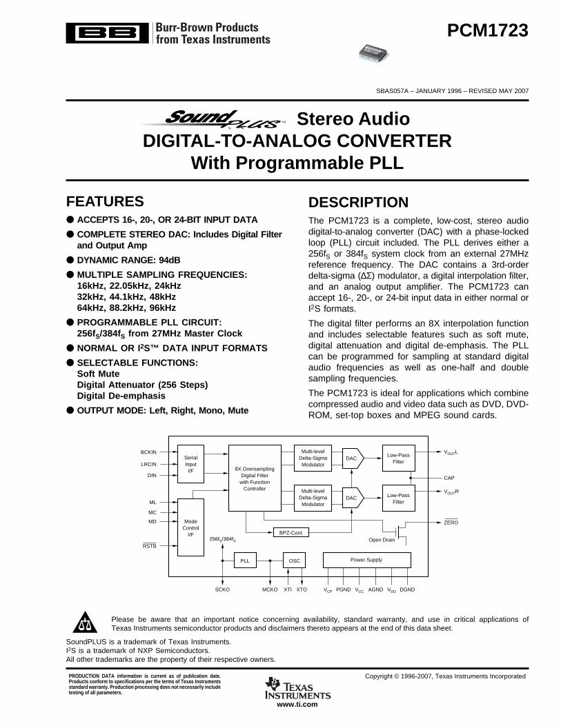
Stereo Audio DIGITAL-TO-ANALOG CONVERTER With Programmable PLL TM 49% FPO PCM1723 FEATURES ● ACCEPTS 16-, 20-, OR 24-BIT INPUT DATA ● COMPLETE STEREO DAC: Includes Digital Filter and Output Amp ● DYNAMIC RANGE: 94dB ● MULTIPLE SAMPLING FREQUENCIES: 16kHz, 22.05kHz, 24kHz 32kHz, 44.1kHz, 48kHz 64kHz, 88.2kHz, 96kHz ● PROGRAMMABLE PLL CIRCUIT: 256f S /384f S from 27MHz Master Clock ● NORMAL OR I 2 S™ DATA INPUT FORMATS ● SELECTABLE FUNCTIONS: Soft Mute Digital Attenuator (256 Steps) Digital De-emphasis ● OUTPUT MODE: Left, Right, Mono, Mute DESCRIPTION The PCM1723 is a complete, low-cost, stereo audio digital-to-analog converter (DAC) with a phase-locked loop (PLL) circuit included. The PLL derives either a 256f S or 384f S system clock from an external 27MHz reference frequency. The DAC contains a 3rd-order delta-sigma (∆Σ) modulator, a digital interpolation filter, and an analog output amplifier. The PCM1723 can accept 16-, 20-, or 24-bit input data in either normal or I 2 S formats. The digital filter performs an 8X interpolation function and includes selectable features such as soft mute, digital attenuation and digital de-emphasis. The PLL can be programmed for sampling at standard digital audio frequencies as well as one-half and double sampling frequencies. The PCM1723 is ideal for applications which combine compressed audio and video data such as DVD, DVD- ROM, set-top boxes and MPEG sound cards. Serial Input I/F Mode Control I/F 8X Oversampling Digital Filter with Function Controller PLL OSC 256f S /384f S V CP PGND V CC AGND Multi-level Delta-Sigma Modulator V OUT L CAP Open Drain DAC Multi-level Delta-Sigma Modulator Low-Pass Filter Low-Pass Filter BPZ-Cont. V OUT R ZERO DAC MC MD ML LRCIN DIN BCKIN RSTB Power Supply XTI XTO V DD DGND MCKO SCKO PCM1723E SBAS057A – JANUARY 1996 – REVISED MAY 2007 www.ti.com PRODUCTION DATA information is current as of publication date. Products conform to specifications per the terms of Texas Instruments standard warranty. Production processing does not necessarily include testing of all parameters. Copyright © 1996-2007, Texas Instruments Incorporated Please be aware that an important notice concerning availability, standard warranty, and use in critical applications of Texas Instruments semiconductor products and disclaimers thereto appears at the end of this data sheet. SoundPLUS is a trademark of Texas Instruments. I 2 S is a trademark of NXP Semiconductors. All other trademarks are the property of their respective owners.

Welcome message from author
This document is posted to help you gain knowledge. Please leave a comment to let me know what you think about it! Share it to your friends and learn new things together.
Transcript
Stereo AudioDIGITAL-TO-ANALOG CONVERTER
With Programmable PLL
TM
49%FPO
PCM1723
FEATURES ACCEPTS 16-, 20-, OR 24-BIT INPUT DATA
COMPLETE STEREO DAC: Includes Digital Filterand Output Amp
DYNAMIC RANGE: 94dB
MULTIPLE SAMPLING FREQUENCIES:16kHz, 22.05kHz, 24kHz32kHz, 44.1kHz, 48kHz64kHz, 88.2kHz, 96kHz
PROGRAMMABLE PLL CIRCUIT:256fS/384fS from 27MHz Master Clock
NORMAL OR I2S™ DATA INPUT FORMATS
SELECTABLE FUNCTIONS:Soft MuteDigital Attenuator (256 Steps)Digital De-emphasis
OUTPUT MODE: Left, Right, Mono, Mute
DESCRIPTIONThe PCM1723 is a complete, low-cost, stereo audiodigital-to-analog converter (DAC) with a phase-lockedloop (PLL) circuit included. The PLL derives either a256fS or 384fS system clock from an external 27MHzreference frequency. The DAC contains a 3rd-orderdelta-sigma (∆Σ) modulator, a digital interpolation filter,and an analog output amplifier. The PCM1723 canaccept 16-, 20-, or 24-bit input data in either normal orI2S formats.
The digital filter performs an 8X interpolation functionand includes selectable features such as soft mute,digital attenuation and digital de-emphasis. The PLLcan be programmed for sampling at standard digitalaudio frequencies as well as one-half and doublesampling frequencies.
The PCM1723 is ideal for applications which combinecompressed audio and video data such as DVD, DVD-ROM, set-top boxes and MPEG sound cards.
SerialInputI/F
ModeControl
I/F
8X OversamplingDigital Filter
with FunctionController
PLL OSC
256fS/384fS
VCP PGND VCC AGND
Multi-levelDelta-SigmaModulator
VOUTL
CAP
Open Drain
DAC
Multi-levelDelta-SigmaModulator
Low-PassFilter
Low-PassFilter
BPZ-Cont.
VOUTR
ZERO
DAC
MC
MD
ML
LRCIN
DIN
BCKIN
RSTB
Power Supply
XTI XTO VDD DGNDMCKOSCKO
PCM1723E
SBAS057A – JANUARY 1996 – REVISED MAY 2007
www.ti.com
PRODUCTION DATA information is current as of publication date.Products conform to specifications per the terms of Texas Instrumentsstandard warranty. Production processing does not necessarily includetesting of all parameters.
Copyright © 1996-2007, Texas Instruments Incorporated
Please be aware that an important notice concerning availability, standard warranty, and use in critical applications ofTexas Instruments semiconductor products and disclaimers thereto appears at the end of this data sheet.
SoundPLUS is a trademark of Texas Instruments.I2S is a trademark of NXP Semiconductors.All other trademarks are the property of their respective owners.
PCM17232SBAS057Awww.ti.com
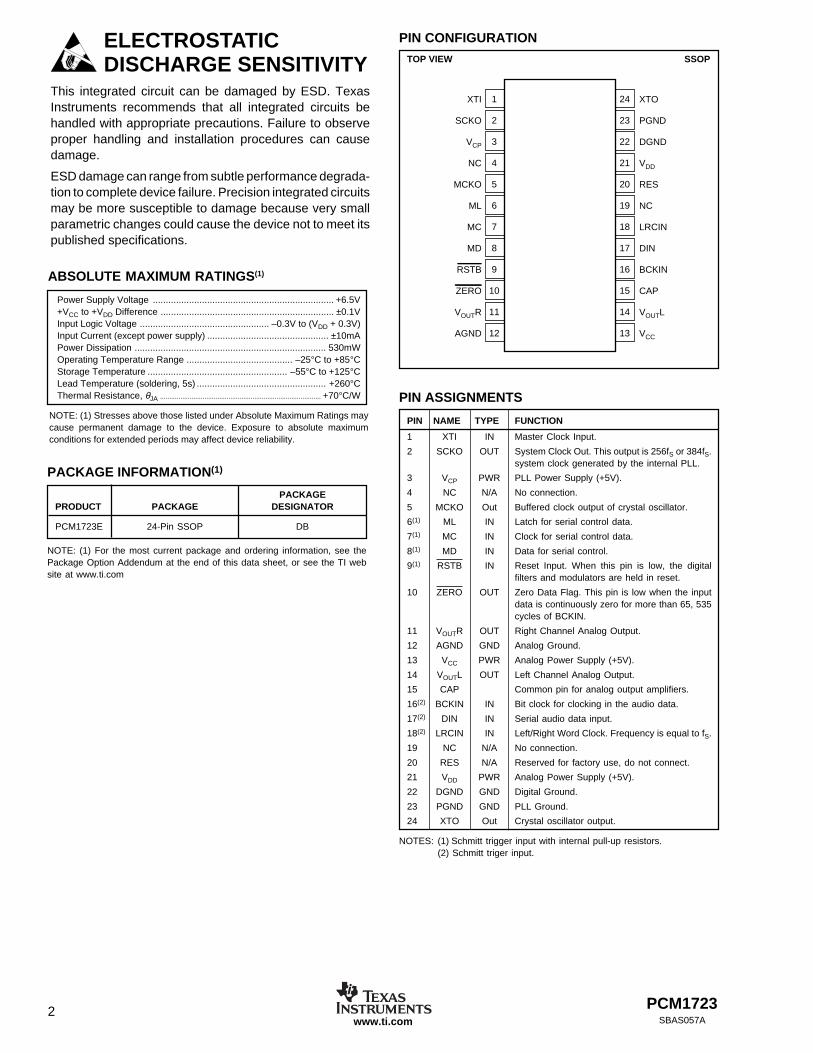
PIN NAME TYPE FUNCTION
1 XTI IN Master Clock Input.
2 SCKO OUT System Clock Out. This output is 256fS or 384fS.system clock generated by the internal PLL.
3 VCP PWR PLL Power Supply (+5V).
4 NC N/A No connection.
5 MCKO Out Buffered clock output of crystal oscillator.
6(1) ML IN Latch for serial control data.
7(1) MC IN Clock for serial control data.
8(1) MD IN Data for serial control.
9(1) RSTB IN Reset Input. When this pin is low, the digitalfilters and modulators are held in reset.
10 ZERO OUT Zero Data Flag. This pin is low when the inputdata is continuously zero for more than 65, 535cycles of BCKIN.
11 VOUTR OUT Right Channel Analog Output.
12 AGND GND Analog Ground.
13 VCC PWR Analog Power Supply (+5V).
14 VOUTL OUT Left Channel Analog Output.
15 CAP Common pin for analog output amplifiers.
16(2) BCKIN IN Bit clock for clocking in the audio data.
17(2) DIN IN Serial audio data input.
18(2) LRCIN IN Left/Right Word Clock. Frequency is equal to fS.
19 NC N/A No connection.
20 RES N/A Reserved for factory use, do not connect.
21 VDD PWR Analog Power Supply (+5V).
22 DGND GND Digital Ground.
23 PGND GND PLL Ground.
24 XTO Out Crystal oscillator output.
NOTES: (1) Schmitt trigger input with internal pull-up resistors.(2) Schmitt triger input.
PIN ASSIGNMENTS
PIN CONFIGURATION
TOP VIEW SSOP
PACKAGE INFORMATION(1)
PACKAGEPRODUCT PACKAGE DESIGNATOR
PCM1723E 24-Pin SSOP DB
NOTE: (1) For the most current package and ordering information, see thePackage Option Addendum at the end of this data sheet, or see the TI website at www.ti.com
ABSOLUTE MAXIMUM RATINGS(1)
Power Supply Voltage ...................................................................... +6.5V+VCC to +VDD Difference ................................................................... ±0.1VInput Logic Voltage .................................................. –0.3V to (VDD + 0.3V)Input Current (except power supply) ............................................... ±10mAPower Dissipation .......................................................................... 530mWOperating Temperature Range ......................................... –25°C to +85°CStorage Temperature ...................................................... –55°C to +125°CLead Temperature (soldering, 5s) .................................................. +260°CThermal Resistance, θJA ....................................................................................... +70°C/W
NOTE: (1) Stresses above those listed under Absolute Maximum Ratings maycause permanent damage to the device. Exposure to absolute maximumconditions for extended periods may affect device reliability.
XTI
SCKO
VCP
NC
MCKO
ML
MC
MD
RSTB
ZERO
VOUTR
AGND
XTO
PGND
DGND
VDD
RES
NC
LRCIN
DIN
BCKIN
CAP
VOUTL
VCC
1
2
3
4
5
6
7
8
9
10
11
12
24
23
22
21
20
19
18
17
16
15
14
13
ELECTROSTATICDISCHARGE SENSITIVITY
This integrated circuit can be damaged by ESD. TexasInstruments recommends that all integrated circuits behandled with appropriate precautions. Failure to observeproper handling and installation procedures can causedamage.
ESD damage can range from subtle performance degrada-tion to complete device failure. Precision integrated circuitsmay be more susceptible to damage because very smallparametric changes could cause the device not to meet itspublished specifications.
PCM1723 3SBAS057A www.ti.com
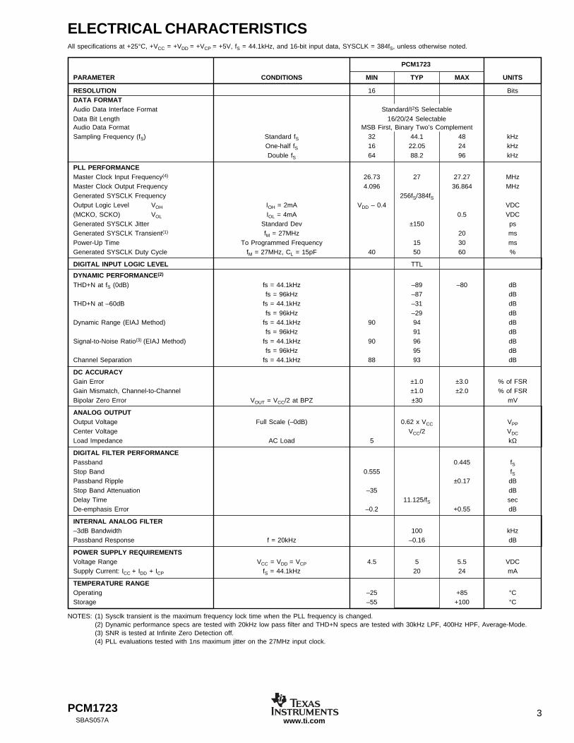
ELECTRICAL CHARACTERISTICSAll specifications at +25°C, +VCC = +VDD = +VCP = +5V, fS = 44.1kHz, and 16-bit input data, SYSCLK = 384fS, unless otherwise noted.
PCM1723
PARAMETER CONDITIONS MIN TYP MAX UNITS
RESOLUTION 16 BitsDATA FORMATAudio Data Interface Format Standard/I2S SelectableData Bit Length 16/20/24 SelectableAudio Data Format MSB First, Binary Two’s ComplementSampling Frequency (fS) Standard fS 32 44.1 48 kHz
One-half fS 16 22.05 24 kHzDouble fS 64 88.2 96 kHz
PLL PERFORMANCEMaster Clock Input Frequency(4) 26.73 27 27.27 MHzMaster Clock Output Frequency 4.096 36.864 MHzGenerated SYSCLK Frequency 256fS/384fSOutput Logic Level VOH IOH = 2mA VDD – 0.4 VDC(MCKO, SCKO) VOL IOL = 4mA 0.5 VDCGenerated SYSCLK Jitter Standard Dev ±150 psGenerated SYSCLK Transient(1) fM = 27MHz 20 msPower-Up Time To Programmed Frequency 15 30 msGenerated SYSCLK Duty Cycle fM = 27MHz, CL = 15pF 40 50 60 %
DIGITAL INPUT LOGIC LEVEL TTL
DYNAMIC PERFORMANCE(2)
THD+N at fS (0dB) fs = 44.1kHz –89 –80 dBfs = 96kHz –87 dB
THD+N at –60dB fs = 44.1kHz –31 dBfs = 96kHz –29 dB
Dynamic Range (EIAJ Method) fs = 44.1kHz 90 94 dBfs = 96kHz 91 dB
Signal-to-Noise Ratio(3) (EIAJ Method) fs = 44.1kHz 90 96 dBfs = 96kHz 95 dB
Channel Separation fs = 44.1kHz 88 93 dB
DC ACCURACYGain Error ±1.0 ±3.0 % of FSRGain Mismatch, Channel-to-Channel ±1.0 ±2.0 % of FSRBipolar Zero Error VOUT = VCC/2 at BPZ ±30 mV
ANALOG OUTPUTOutput Voltage Full Scale (–0dB) 0.62 x VCC VPP
Center Voltage VCC/2 VDC
Load Impedance AC Load 5 kΩ
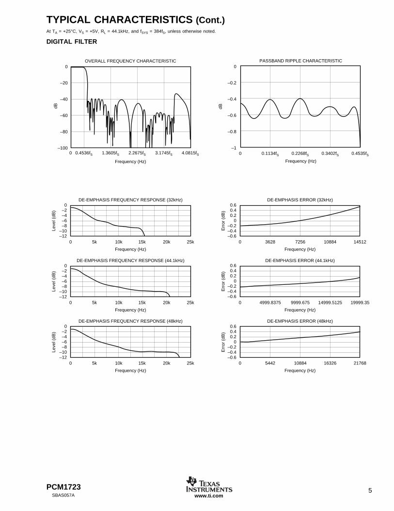
DIGITAL FILTER PERFORMANCEPassband 0.445 fSStop Band 0.555 fSPassband Ripple ±0.17 dBStop Band Attenuation –35 dBDelay Time 11.125/fS secDe-emphasis Error –0.2 +0.55 dB
INTERNAL ANALOG FILTER–3dB Bandwidth 100 kHzPassband Response f = 20kHz –0.16 dB
POWER SUPPLY REQUIREMENTSVoltage Range VCC = VDD = VCP 4.5 5 5.5 VDCSupply Current: ICC + IDD + ICP fS = 44.1kHz 20 24 mA
TEMPERATURE RANGEOperating –25 +85 °CStorage –55 +100 °C
NOTES: (1) Sysclk transient is the maximum frequency lock time when the PLL frequency is changed.(2) Dynamic performance specs are tested with 20kHz low pass filter and THD+N specs are tested with 30kHz LPF, 400Hz HPF, Average-Mode.(3) SNR is tested at Infinite Zero Detection off.(4) PLL evaluations tested with 1ns maximum jitter on the 27MHz input clock.
PCM17234SBAS057Awww.ti.com
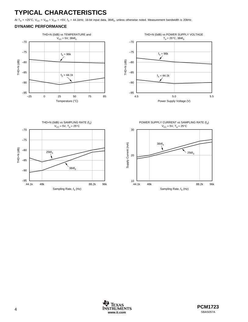
TYPICAL CHARACTERISTICSAt TA = +25°C, VCC = VDD = VCP = +5V, fS = 44.1kHz, 16-bit input data, 384fS, unless otherwise noted. Measurement bandwidth is 20kHz.
DYNAMIC PERFORMANCE
THD+N (0dB) vs TEMPERATURE and VCC = 5V, 384fS
Temperature (°C)
TH
D+
N (
dB)
–70
–75
–80
–85
–90
–95–25 0 25 50 75 85
fS = 96k
fS = 44.1k
THD+N (0dB) vs POWER SUPPLY VOLTAGE TA = 25°C, 384fS
Power Supply Voltage (V)
TH
D+
N (
dB)
–70
–75
–80
–85
–90
–954.5 5.0 5.5
fS = 96k
fS = 44.1k
THD+N (0dB) vs SAMPLING RATE (fS) VCC = 5V, TA = 25°C
Sampling Rate, fS (Hz)
TH
D+
N (
dB)
–70
–75
–80
–85
–90
–9544.1k 48k 88.2k 96k
256fS
384fS
POWER SUPPLY CURRENT vs SAMPLING RATE (fS) VCC = 5V, TA = 25°C
Sampling Rate, fS (Hz)
Sup
ply
Cur
rent
(m
A)
30
20
1044.1k 48k 88.2k 96k
384fS
256fS
PCM1723 5SBAS057A www.ti.com
PASSBAND RIPPLE CHARACTERISTIC0
–0.2
–0.4
–0.6
–0.8
–10 0.1134fS 0.2268fS 0.3402fS 0.4535fS
dB
Frequency (Hz)
TYPICAL CHARACTERISTICS (Cont.)At TA = +25°C, VS = +5V, RL = 44.1kHz, and fSYS = 384fS, unless otherwise noted.
DIGITAL FILTER
0 0.4536fS 1.3605fS 2.2675fS 3.1745fS 4.0815fS
0
–20
–40
–60
–80
–100
dBOVERALL FREQUENCY CHARACTERISTIC
Frequency (Hz)
DE-EMPHASIS FREQUENCY RESPONSE (32kHz)
0 5k 10k 15k 20k 25k
Frequency (Hz)
0–2–4–6–8
–10–12
DE-EMPHASIS FREQUENCY RESPONSE (44.1kHz)
0 5k 10k 15k 20k 25k
Frequency (Hz)
0–2–4–6–8
–10–12
DE-EMPHASIS FREQUENCY RESPONSE (48kHz)
0 5k 10k 15k 20k 25k
Frequency (Hz)
0–2–4–6–8
–10–12
Leve
l (dB
)Le
vel (
dB)
Leve
l (dB
)
DE-EMPHASIS ERROR (32kHz)
0 3628 7256 10884 14512
0 4999.8375 9999.675 14999.5125 19999.35
0 5442 10884 16326 21768
Frequency (Hz)
0.60.40.2
0–0.2–0.4–0.6
0.60.40.2
0–0.2–0.4–0.6
0.60.40.2
0–0.2–0.4–0.6
DE-EMPHASIS ERROR (44.1kHz)
Frequency (Hz)
DE-EMPHASIS ERROR (48kHz)
Frequency (Hz)
Err
or (
dB)
Err
or (
dB)
Err
or (
dB)
PCM17236SBAS057Awww.ti.com
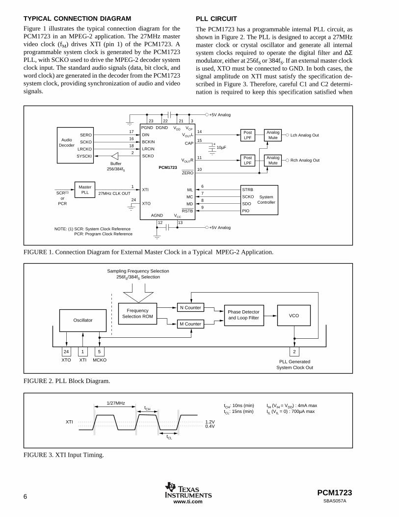
TYPICAL CONNECTION DIAGRAM
Figure 1 illustrates the typical connection diagram for thePCM1723 in an MPEG-2 application. The 27MHz mastervideo clock (fM) drives XTI (pin 1) of the PCM1723. Aprogrammable system clock is generated by the PCM1723PLL, with SCKO used to drive the MPEG-2 decoder systemclock input. The standard audio signals (data, bit clock, andword clock) are generated in the decoder from the PCM1723system clock, providing synchronization of audio and videosignals.
PLL CIRCUIT
The PCM1723 has a programmable internal PLL circuit, asshown in Figure 2. The PLL is designed to accept a 27MHzmaster clock or crystal oscillator and generate all internalsystem clocks required to operate the digital filter and ∆Σmodulator, either at 256fS or 384fS. If an external master clockis used, XTO must be connected to GND. In both cases, thesignal amplitude on XTI must satisfy the specification de-scribed in Figure 3. Therefore, careful C1 and C2 determi-nation is required to keep this specification satisfied when
FIGURE 1. Connection Diagram for External Master Clock in a Typical MPEG-2 Application.
Oscillator
XTO XTI MCKO PLL GeneratedSystem Clock Out
FrequencySelection ROM
Phase Detectorand Loop Filter VCO
Sampling Frequency Selection256fS/384fS Selection
N Counter
M Counter
24 1 5 2
FIGURE 2. PLL Block Diagram.
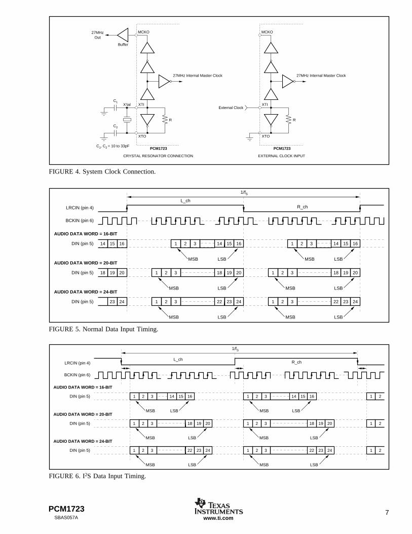
FIGURE 3. XTI Input Timing.
tCH
XTI
1/27MHz
tCL
1.2V
tCH: 10ns (min)tCL: 15ns (min)
IIH (VIH = VDD) : 4mA maxIIL (VIL = 0) : 700µA max
0.4V
DIN
BCKIN
LRCIN
SCKO
SERO
SCKO
LRCKO
SYSCKI
XTI
17
16
18
2
6
7
8
9
ML
MC
MD
RSTB
14
XTO
23 22 21 3
11
15
10
1
24
27MHz CLK OUT
+10µF
PostLPF
PostLPF
AnalogMute
AnalogMute
STRB
SCKO
SDO
PIO
SystemController
Rch Analog Out
Lch Analog Out
12 13
AudioDecoder
Buffer256/384fS
AGND
PGND DGND
VCC
+5V Analog
+5V Analog
VDD VCP
VOUTL
VOUTR
ZERO
CAP
PCM1723
MasterPLLSCR(1)
orPCR
NOTE: (1) SCR: System Clock ReferencePCR: Program Clock Reference
PCM1723 7SBAS057A www.ti.com
FIGURE 4. System Clock Connection.
14 15 16 1 2 3 14 15
1/fS
L_chR_ch
MSB LSB
16
LRCIN (pin 4)
BCKIN (pin 6)
AUDIO DATA WORD = 16-BIT
DIN (pin 5) 1 2 3 14 15
MSB LSB
16
18 19 20 1 2 3 18 19
MSB LSB
20
AUDIO DATA WORD = 20-BIT
DIN (pin 5) 1 2 3 18 19
MSB LSB
20
23 24 1 2 3 22 23
MSB LSB
24
AUDIO DATA WORD = 24-BIT
DIN (pin 5) 1 2 3 22 23
MSB LSB
24
FIGURE 5. Normal Data Input Timing.
1 2 3 14 15
1/fS
L_chR_ch
MSB LSB
16
LRCIN (pin 4)
BCKIN (pin 6)
AUDIO DATA WORD = 16-BIT
DIN (pin 5) 1 2 3 14 15
MSB LSB
16
1 2 3 18 19
MSB LSB
20
AUDIO DATA WORD = 20-BIT
DIN (pin 5) 1 2 3 18 19
MSB LSB
20
21
21
211 2 3 22 23
MSB LSB
24
AUDIO DATA WORD = 24-BIT
DIN (pin 5) 1 2 3 22 23
MSB LSB
24
FIGURE 6. I2S Data Input Timing.
C1
C2
C1, C2 = 10 to 33pF
27MHz Internal Master Clock
XTIX’tal
R R
XTO
PCM1723
MCKO
Buffer
27MHzOut
External Clock
27MHz Internal Master Clock
XTI
XTO
PCM1723
EXTERNAL CLOCK INPUTCRYSTAL RESONATOR CONNECTION
MCKO
PCM17238SBAS057Awww.ti.com
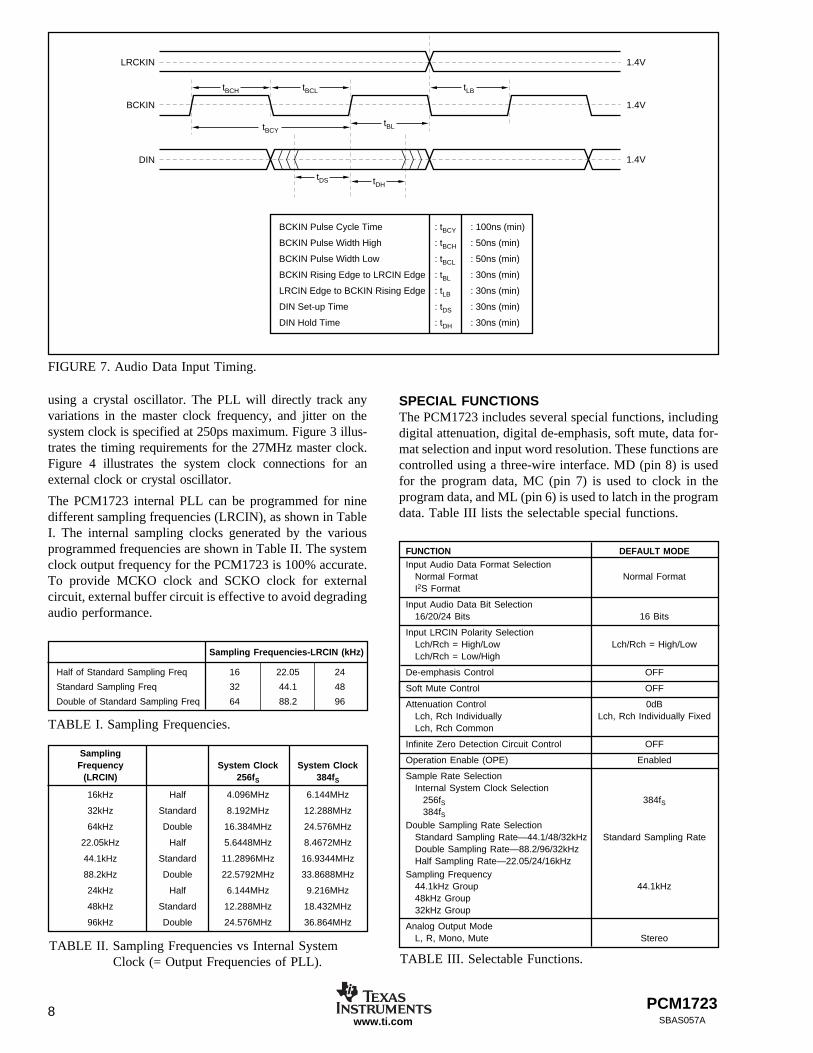
FIGURE 7. Audio Data Input Timing.
using a crystal oscillator. The PLL will directly track anyvariations in the master clock frequency, and jitter on thesystem clock is specified at 250ps maximum. Figure 3 illus-trates the timing requirements for the 27MHz master clock.Figure 4 illustrates the system clock connections for anexternal clock or crystal oscillator.
The PCM1723 internal PLL can be programmed for ninedifferent sampling frequencies (LRCIN), as shown in TableI. The internal sampling clocks generated by the variousprogrammed frequencies are shown in Table II. The systemclock output frequency for the PCM1723 is 100% accurate.To provide MCKO clock and SCKO clock for externalcircuit, external buffer circuit is effective to avoid degradingaudio performance.
SPECIAL FUNCTIONSThe PCM1723 includes several special functions, includingdigital attenuation, digital de-emphasis, soft mute, data for-mat selection and input word resolution. These functions arecontrolled using a three-wire interface. MD (pin 8) is usedfor the program data, MC (pin 7) is used to clock in theprogram data, and ML (pin 6) is used to latch in the programdata. Table III lists the selectable special functions.
FUNCTION DEFAULT MODEInput Audio Data Format Selection
Normal Format Normal FormatI2S Format
Input Audio Data Bit Selection16/20/24 Bits 16 Bits
Input LRCIN Polarity SelectionLch/Rch = High/Low Lch/Rch = High/LowLch/Rch = Low/High
De-emphasis Control OFF
Soft Mute Control OFF
Attenuation Control 0dBLch, Rch Individually Lch, Rch Individually FixedLch, Rch Common
Infinite Zero Detection Circuit Control OFF
Operation Enable (OPE) Enabled
Sample Rate SelectionInternal System Clock Selection
256fS 384fS384fS
Double Sampling Rate SelectionStandard Sampling Rate—44.1/48/32kHz Standard Sampling RateDouble Sampling Rate—88.2/96/32kHzHalf Sampling Rate—22.05/24/16kHz
Sampling Frequency44.1kHz Group 44.1kHz48kHz Group32kHz Group
Analog Output ModeL, R, Mono, Mute Stereo
TABLE III. Selectable Functions.
Sampling Frequencies-LRCIN (kHz)
Half of Standard Sampling Freq 16 22.05 24
Standard Sampling Freq 32 44.1 48
Double of Standard Sampling Freq 64 88.2 96
TABLE I. Sampling Frequencies.
SamplingFrequency System Clock System Clock
(LRCIN) 256fS 384fS
16kHz Half 4.096MHz 6.144MHz
32kHz Standard 8.192MHz 12.288MHz
64kHz Double 16.384MHz 24.576MHz
22.05kHz Half 5.6448MHz 8.4672MHz
44.1kHz Standard 11.2896MHz 16.9344MHz
88.2kHz Double 22.5792MHz 33.8688MHz
24kHz Half 6.144MHz 9.216MHz
48kHz Standard 12.288MHz 18.432MHz
96kHz Double 24.576MHz 36.864MHz
TABLE II. Sampling Frequencies vs Internal SystemClock (= Output Frequencies of PLL).
LRCKIN
BCKIN
DIN
1.4V
1.4V
1.4V
tBCH tBCL tLB
tBL
tDS
BCKIN Pulse Cycle Time
BCKIN Pulse Width High
BCKIN Pulse Width Low
BCKIN Rising Edge to LRCIN Edge
LRCIN Edge to BCKIN Rising Edge
DIN Set-up Time
DIN Hold Time
: tBCY
: tBCH
: tBCL
: tBL
: tLB
: tDS
: tDH
: 100ns (min)
: 50ns (min)
: 50ns (min)
: 30ns (min)
: 30ns (min)
: 30ns (min)
: 30ns (min)
tDH
tBCY
PCM1723 9SBAS057A www.ti.com
level until LDL is set to 1. LDR in Register 1 has the samefunction for right channel attenuation.
Attenuation Level (ATT) can be controlled as followingResistor set AL (R) (7:0).
AL (R) (7:0) ATT LEVEL
00h –∞dB (Mute)01h –48.16dB
. .
. .
. .FEh –0.07dBFFh 0dB
REGISTER 1 (A1 = 0, A0 = 1)
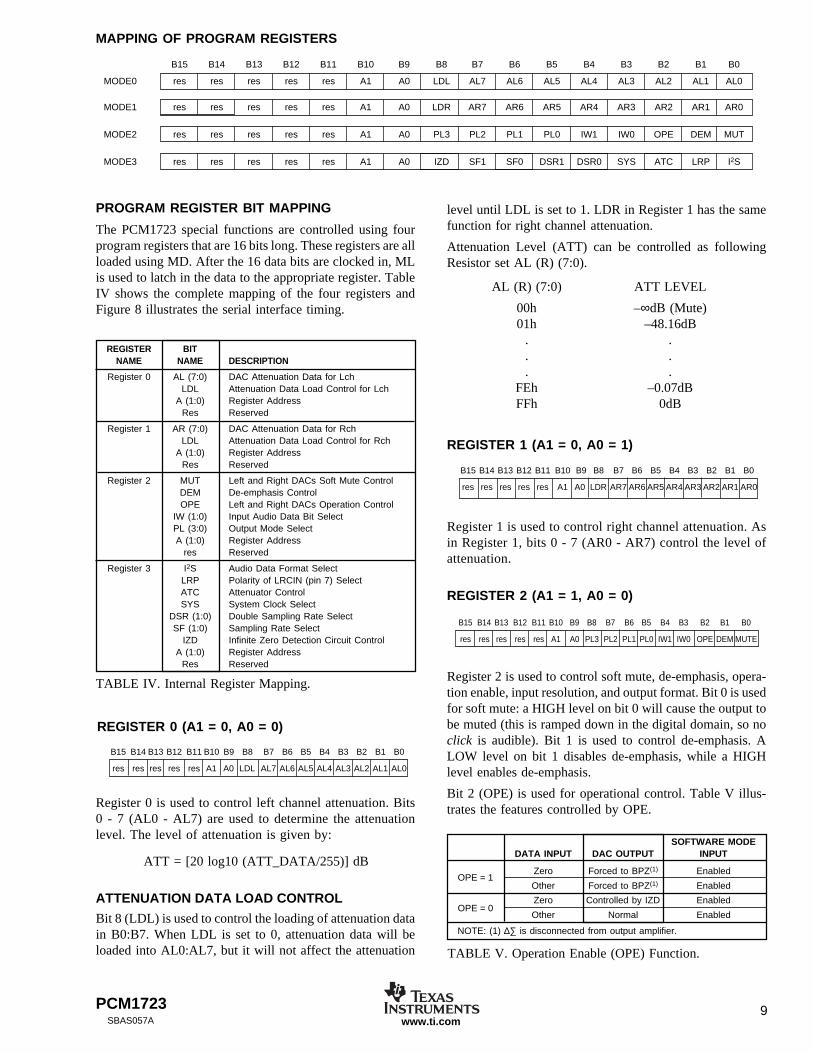
MAPPING OF PROGRAM REGISTERS
B15 B14 B13 B12 B11 B10 B9 B8 B7 B6 B5 B4 B3 B2 B1 B0
MODE0 res res res res res A1 A0 LDL AL7 AL6 AL5 AL4 AL3 AL2 AL1 AL0
MODE1 res res res res res A1 A0 LDR AR7 AR6 AR5 AR4 AR3 AR2 AR1 AR0
MODE2 res res res res res A1 A0 PL3 PL2 PL1 PL0 IW1 IW0 OPE DEM MUT
MODE3 res res res res res A1 A0 IZD SF1 SF0 DSR1 DSR0 SYS ATC LRP I2S
PROGRAM REGISTER BIT MAPPING
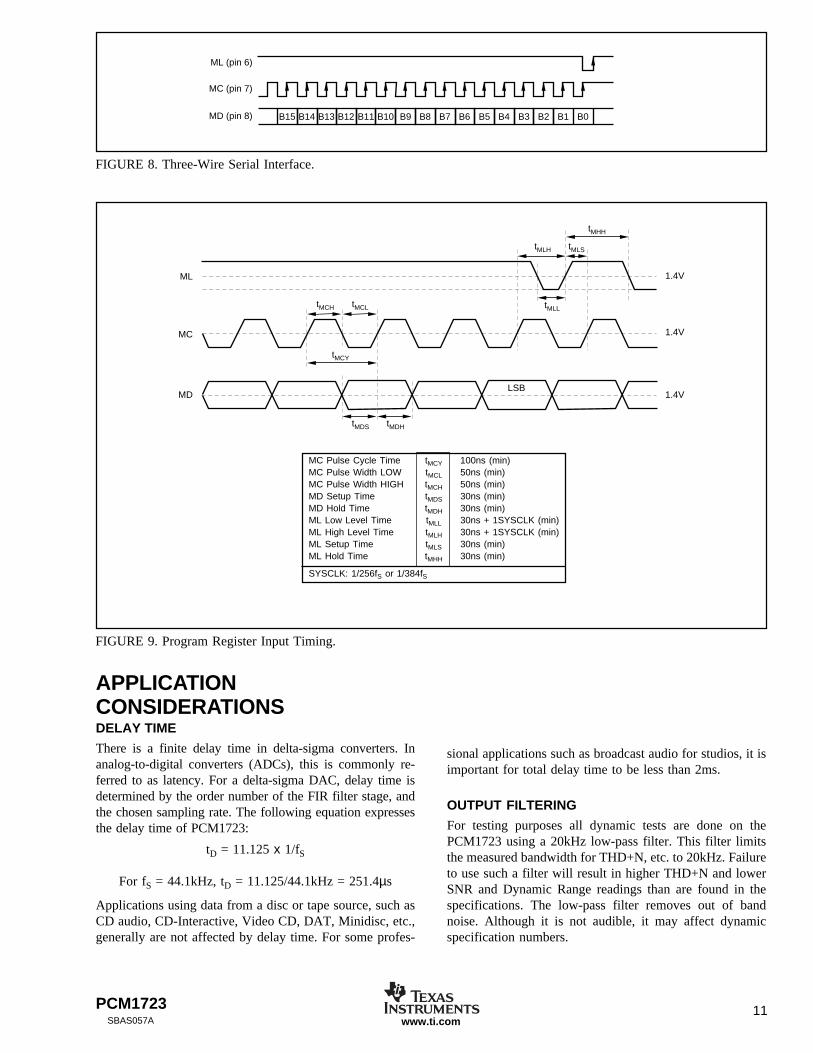
The PCM1723 special functions are controlled using fourprogram registers that are 16 bits long. These registers are allloaded using MD. After the 16 data bits are clocked in, MLis used to latch in the data to the appropriate register. TableIV shows the complete mapping of the four registers andFigure 8 illustrates the serial interface timing.
REGISTER BITNAME NAME DESCRIPTION
Register 0 AL (7:0) DAC Attenuation Data for LchLDL Attenuation Data Load Control for Lch
A (1:0) Register AddressRes Reserved
Register 1 AR (7:0) DAC Attenuation Data for RchLDL Attenuation Data Load Control for Rch
A (1:0) Register AddressRes Reserved
Register 2 MUT Left and Right DACs Soft Mute ControlDEM De-emphasis ControlOPE Left and Right DACs Operation Control
IW (1:0) Input Audio Data Bit SelectPL (3:0) Output Mode SelectA (1:0) Register Address
res Reserved
Register 3 I2S Audio Data Format SelectLRP Polarity of LRCIN (pin 7) SelectATC Attenuator ControlSYS System Clock Select
DSR (1:0) Double Sampling Rate SelectSF (1:0) Sampling Rate Select
IZD Infinite Zero Detection Circuit ControlA (1:0) Register Address
Res Reserved
TABLE IV. Internal Register Mapping.
REGISTER 0 (A1 = 0, A0 = 0)
B15 B14 B13 B12 B11 B10 B9 B8 B7 B6 B5 B4 B3 B2 B1 B0
res res res res res A1 A0 LDL AL7 AL6 AL5 AL4 AL3 AL2 AL1 AL0
Register 0 is used to control left channel attenuation. Bits0 - 7 (AL0 - AL7) are used to determine the attenuationlevel. The level of attenuation is given by:
ATT = [20 log10 (ATT_DATA/255)] dB
ATTENUATION DATA LOAD CONTROL
Bit 8 (LDL) is used to control the loading of attenuation datain B0:B7. When LDL is set to 0, attenuation data will beloaded into AL0:AL7, but it will not affect the attenuation
B15 B14 B13 B12 B11 B10 B9 B8 B7 B6 B5 B4 B3 B2 B1 B0
res res res res res A1 A0 LDR AR7 AR6 AR5 AR4 AR3 AR2 AR1 AR0
Register 1 is used to control right channel attenuation. Asin Register 1, bits 0 - 7 (AR0 - AR7) control the level ofattenuation.
REGISTER 2 (A1 = 1, A0 = 0)
B15 B14 B13 B12 B11 B10 B9 B8 B7 B6 B5 B4 B3 B2 B1 B0
res res res res res A1 A0 PL3 PL2 PL1 PL0 IW1 IW0 OPE DEM MUTE
Register 2 is used to control soft mute, de-emphasis, opera-tion enable, input resolution, and output format. Bit 0 is usedfor soft mute: a HIGH level on bit 0 will cause the output tobe muted (this is ramped down in the digital domain, so noclick is audible). Bit 1 is used to control de-emphasis. ALOW level on bit 1 disables de-emphasis, while a HIGHlevel enables de-emphasis.
Bit 2 (OPE) is used for operational control. Table V illus-trates the features controlled by OPE.
SOFTWARE MODEDATA INPUT DAC OUTPUT INPUT
Zero Forced to BPZ(1) Enabled
Other Forced to BPZ(1) Enabled
Zero Controlled by IZD Enabled
Other Normal Enabled
OPE = 1
OPE = 0
TABLE V. Operation Enable (OPE) Function.
NOTE: (1) ∆∑ is disconnected from output amplifier.
PCM172310SBAS057Awww.ti.com
OPE controls the operation of the DAC: when OPE is LOW,the DAC will convert all non-zero input data. If the inputdata is continuously zero for 65,536 cycles of BCKIN, theoutput will be forced to zero only if IZD is HIGH. WhenOPE is HIGH, the output of the DAC will be forced tobipolar zero, irrespective of any input data.
IZD = 1
IZD = 0
DATA INPUT DAC OUTPUT
Zero Forced to BPZ(1)
Other Normal
Zero Zero(2)
Other Normal
TABLE VI. Infinite Zero Detection (IZD) Function.
RSTB = HIGH
RSTB = LOW
SOFTWARE MODE
DATA INPUT DAC OUTPUT INPUT
Zero Controlled by OPE and IZD Enabled
Other Controlled by OPE and IZD Enabled
Zero Forced to BPZ(1) Disabled
Other Forced to BPZ(1) Disabled
TABLE VII. Reset (RSTB) Function.
Bits 3 (IW0) and 4 (IW1) are used to determine input wordresolution. PCM1723 can be set up for input word resolu-tions of 16, 20, or 24 bits:
Bit 4 (IW1) Bit 3 (IW0) Input Resolution
0 0 16-bit Data Word0 1 20-bit Data Word1 0 24-bit Data Word1 1 Reserved
Bits 5, 6, 7, and 8 (PL0:3) are used to control output format.The output of PCM1723 can be programmed for 16 differentstates, as shown in Table VIII.
PL0 PL1 PL2 PL3 Lch OUTPUT Rch OUTPUT NOTE
0 0 0 0 MUTE MUTE MUTE
0 0 0 1 MUTE R
0 0 1 0 MUTE L
0 0 1 1 MUTE (L + R)/2
0 1 0 0 R MUTE
0 1 0 1 R R
0 1 1 0 R L REVERSE
0 1 1 1 R (L + R)/2
1 0 0 0 L MUTE
1 0 0 1 L R STEREO
1 0 1 0 L L
1 0 1 1 L (L + R)/2
1 1 0 0 (L + R)/2 MUTE
1 1 0 1 (L + R)/2 R
1 1 1 0 (L + R)/2 L
1 1 1 1 (L + R)/2 (L + R)/2 MONO
TABLE VIII. Programmable Output Format.
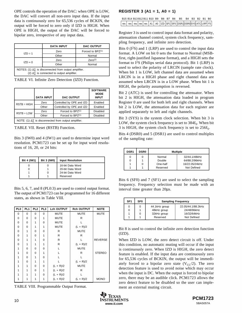
REGISTER 3 (A1 = 1, A0 = 1)
B15 B14 B13 B12 B11 B10 B9 B8 B7 B6 B5 B4 B3 B2 B1 B0
res res res res res A1 A0 IZD SF1 SF0 DSR1 DSR0 SYS ATC LRP I2S
Register 3 is used to control input data format and polarity,attenuation channel control, system clock frequency, sam-pling frequency, and infinite zero detection.
Bits 0 (I2S) and 1 (LRP) are used to control the input dataformat. A LOW on bit 0 sets the format to Normal (MSB-first, right-justified Japanese format), and a HIGH sets theformat to I2S (Philips serial data protocol). Bit 1 (LRP) isused to select the polarity of LRCIN (sample rate clock).When bit 1 is LOW, left channel data are assumed whenLRCIN is in a HIGH phase and right channel data areassumed when LRCIN is in a LOW phase. When bit 1 isHIGH, the polarity assumption is reversed.
Bit 2 (ATC) is used for controlling the attenuator. Whenbit 2 is HIGH, the attenuation data loaded in programRegister 0 are used for both left and right channels. Whenbit 2 is LOW, the attenuation data for each register areapplied separately to left and right channels.
Bit 3 (SYS) is the system clock selection. When bit 3 isLOW, the system clock frequency is set to 384fS. When bit3 is HIGH, the system clock frequency is set to 256fS.
Bits 4 (DSR0) and 5 (DSR1) are used to control multiplesof the sampling rate:
DSR1 DSR0 Multiple
0 0 Normal 32/44.1/48kHz0 1 Double 64/88.2/96kHz1 0 One-half 16/22.05/24kHz1 1 Reserved Not Defined
Bits 6 (SF0) and 7 (SF1) are used to select the samplingfrequency. Frequency selection must be made with aninterval time greater than 20µs.
SF1 SF0 Sampling Frequency
0 0 44.1kHz group 22.05/44.1/88.2kHz0 1 48kHz group 24/48/96kHz1 0 32kHz group 16/32/64kHz1 1 Reserved Not Defined
Bit 8 is used to control the infinite zero detection function(IZD).
When IZD is LOW, the zero detect circuit is off. Underthis condition, no automatic muting will occur if the inputis continuously zero. When IZD is HIGH, the zero detectfeature is enabled. If the input data are continuously zerofor 65,536 cycles of BCKIN, the output will be immedi-ately forced to a bipolar zero state (VCC/2). The zerodetection feature is used to avoid noise which may occurwhen the input is DC. When the output is forced to bipolarzero, there may be an audible click. PCM1723 allows thezero detect feature to be disabled so the user can imple-ment an external muting circuit.
NOTE: (1) ∆∑ is disconnected from output amplifier.
NOTES: (1) ∆∑ is disconnected from output amplifier.(2) ∆∑ is connected to output amplifier.
PCM1723 11SBAS057A www.ti.com
B15 B14 B13 B12 B11 B10 B9 B8 B7 B6 B5 B4 B3 B2 B1 B0
ML (pin 6)
MC (pin 7)
MD (pin 8)
FIGURE 8. Three-Wire Serial Interface.
FIGURE 9. Program Register Input Timing.
APPLICATIONCONSIDERATIONSDELAY TIME
There is a finite delay time in delta-sigma converters. Inanalog-to-digital converters (ADCs), this is commonly re-ferred to as latency. For a delta-sigma DAC, delay time isdetermined by the order number of the FIR filter stage, andthe chosen sampling rate. The following equation expressesthe delay time of PCM1723:
tD = 11.125 x 1/fS
For fS = 44.1kHz, tD = 11.125/44.1kHz = 251.4µs
Applications using data from a disc or tape source, such asCD audio, CD-Interactive, Video CD, DAT, Minidisc, etc.,generally are not affected by delay time. For some profes-
sional applications such as broadcast audio for studios, it isimportant for total delay time to be less than 2ms.
OUTPUT FILTERING
For testing purposes all dynamic tests are done on thePCM1723 using a 20kHz low-pass filter. This filter limitsthe measured bandwidth for THD+N, etc. to 20kHz. Failureto use such a filter will result in higher THD+N and lowerSNR and Dynamic Range readings than are found in thespecifications. The low-pass filter removes out of bandnoise. Although it is not audible, it may affect dynamicspecification numbers.
MC Pulse Cycle Time tMCY 100ns (min)MC Pulse Width LOW tMCL 50ns (min)MC Pulse Width HIGH tMCH 50ns (min)MD Setup Time tMDS 30ns (min)MD Hold Time tMDH 30ns (min)ML Low Level Time tMLL 30ns + 1SYSCLK (min)ML High Level Time tMLH 30ns + 1SYSCLK (min)ML Setup Time tMLS 30ns (min)ML Hold Time tMHH 30ns (min)
SYSCLK: 1/256fS or 1/384fS
1.4V
1.4V
1.4V
ML
MC
MD
tMLL
tMHH
tMCH tMCL
tMDS
tMCY
tMLStMLH
tMDH
LSB
PCM172312SBAS057Awww.ti.com
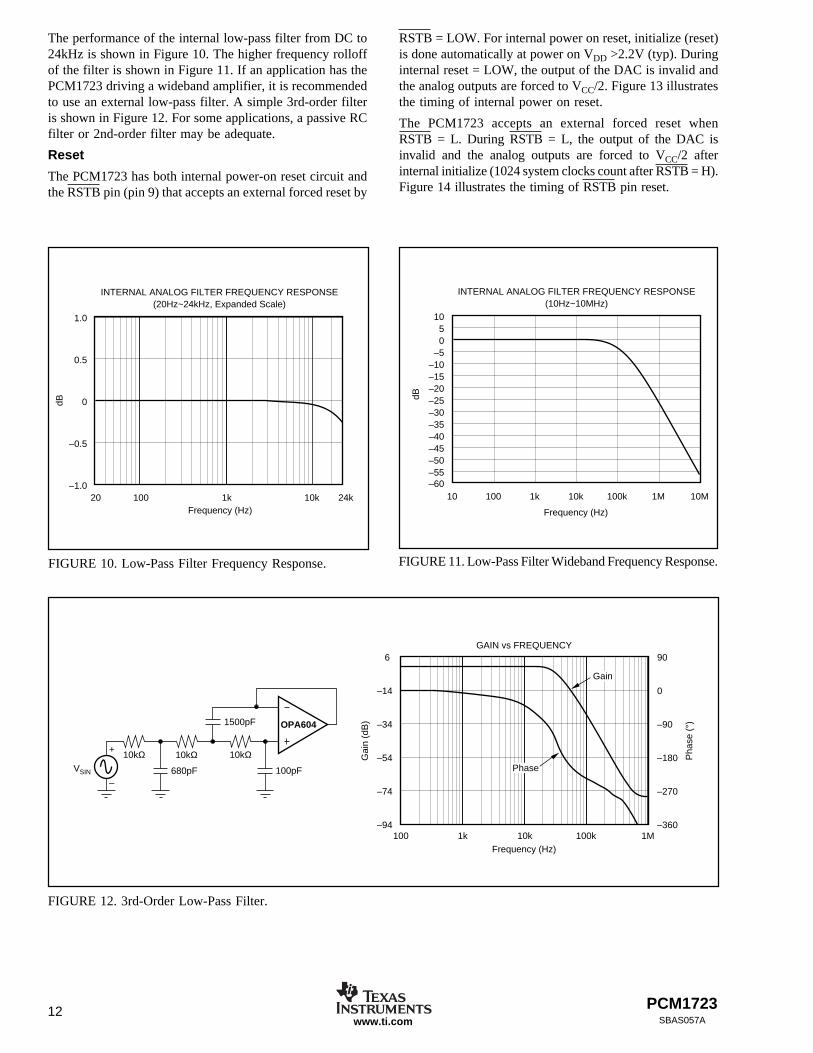
The performance of the internal low-pass filter from DC to24kHz is shown in Figure 10. The higher frequency rolloffof the filter is shown in Figure 11. If an application has thePCM1723 driving a wideband amplifier, it is recommendedto use an external low-pass filter. A simple 3rd-order filteris shown in Figure 12. For some applications, a passive RCfilter or 2nd-order filter may be adequate.
Reset
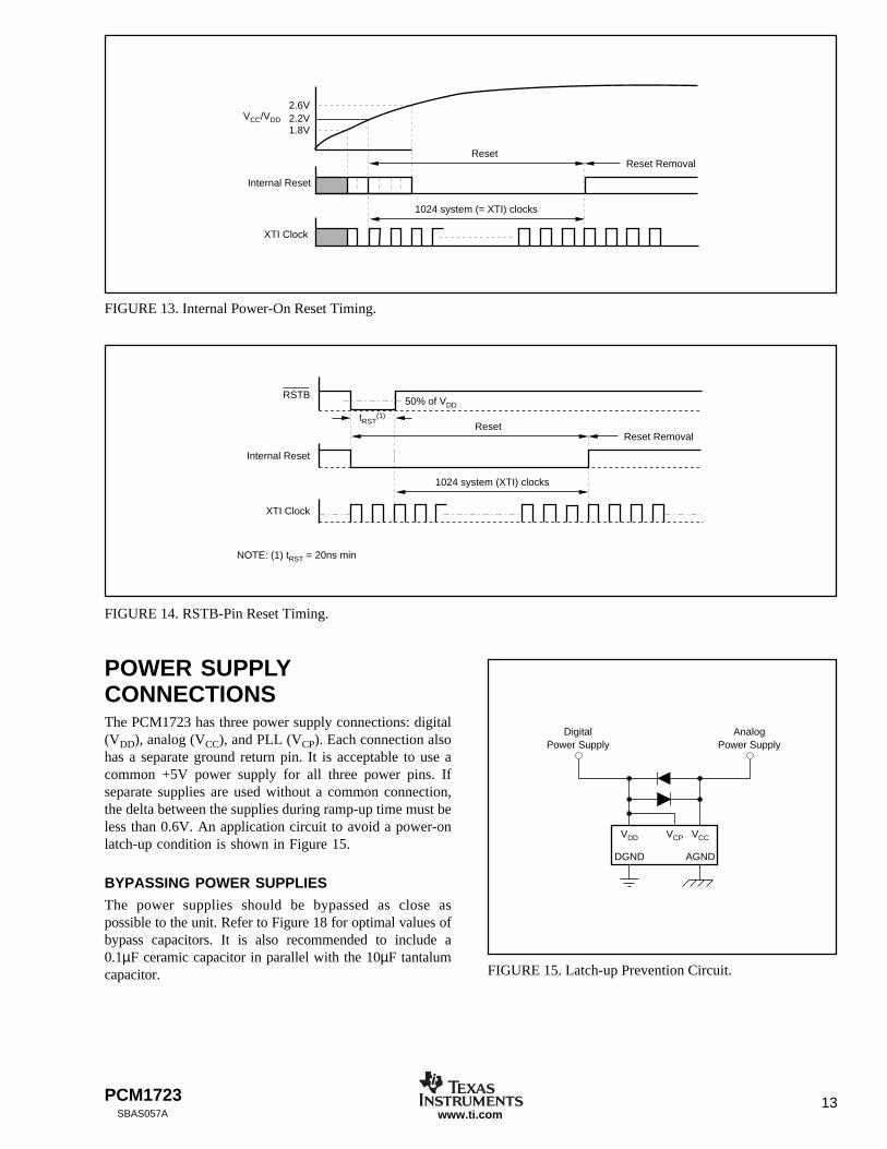
The PCM1723 has both internal power-on reset circuit andthe RSTB pin (pin 9) that accepts an external forced reset by
RSTB = LOW. For internal power on reset, initialize (reset)is done automatically at power on VDD >2.2V (typ). Duringinternal reset = LOW, the output of the DAC is invalid andthe analog outputs are forced to VCC/2. Figure 13 illustratesthe timing of internal power on reset.
The PCM1723 accepts an external forced reset whenRSTB = L. During RSTB = L, the output of the DAC isinvalid and the analog outputs are forced to VCC/2 afterinternal initialize (1024 system clocks count after RSTB = H).Figure 14 illustrates the timing of RSTB pin reset.
FIGURE 12. 3rd-Order Low-Pass Filter.
10kΩ10kΩ10kΩ
1500pF
100pF680pF
+
VSIN
–
90
0
–90
–180
–270
–360100 1k 10k 100k 1M
GAIN vs FREQUENCY
Frequency (Hz)
Pha
se (
°)
6
–14
–34
–54
–74
–94
Gai
n (d
B)
Gain
Phase
OPA604
FIGURE 11. Low-Pass Filter Wideband Frequency Response.FIGURE 10. Low-Pass Filter Frequency Response.
1050
–5–10–15–20–25–30–35–40–45–50–55
10 100 1k 10k 100k 1M 10M
Frequency (Hz)
dB
–60
INTERNAL ANALOG FILTER FREQUENCY RESPONSE(10Hz~10MHz)
1.0
0.5
0
–0.5
–1.0
dB
20Frequency (Hz)
100 1k 10k 24k
INTERNAL ANALOG FILTER FREQUENCY RESPONSE(20Hz~24kHz, Expanded Scale)
PCM1723 13SBAS057A www.ti.com
1024 system (= XTI) clocks
ResetReset Removal
2.6V2.2V1.8V
VCC/VDD
Internal Reset
XTI Clock
FIGURE 14. RSTB-Pin Reset Timing.
1024 system (XTI) clocks
ResetReset Removal
XTI Clock
Internal Reset
RSTB50% of VDD
tRST(1)
NOTE: (1) tRST = 20ns min
FIGURE 13. Internal Power-On Reset Timing.
FIGURE 15. Latch-up Prevention Circuit.
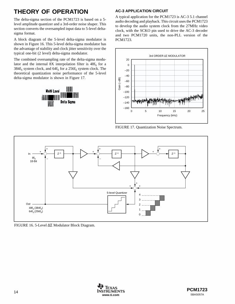
POWER SUPPLYCONNECTIONSThe PCM1723 has three power supply connections: digital(VDD), analog (VCC), and PLL (VCP). Each connection alsohas a separate ground return pin. It is acceptable to use acommon +5V power supply for all three power pins. Ifseparate supplies are used without a common connection,the delta between the supplies during ramp-up time must beless than 0.6V. An application circuit to avoid a power-onlatch-up condition is shown in Figure 15.
BYPASSING POWER SUPPLIES
The power supplies should be bypassed as close aspossible to the unit. Refer to Figure 18 for optimal values ofbypass capacitors. It is also recommended to include a0.1µF ceramic capacitor in parallel with the 10µF tantalumcapacitor.
DGND AGND
VDD VCCVCP
DigitalPower Supply
AnalogPower Supply
PCM172314SBAS057Awww.ti.com
THEORY OF OPERATIONThe delta-sigma section of the PCM1723 is based on a 5-level amplitude quantizer and a 3rd-order noise shaper. Thissection converts the oversampled input data to 5-level delta-sigma format.
A block diagram of the 5-level delta-sigma modulator isshown in Figure 16. This 5-level delta-sigma modulator hasthe advantage of stability and clock jitter sensitivity over thetypical one-bit (2 level) delta-sigma modulator.
The combined oversampling rate of the delta-sigma modu-lator and the internal 8X interpolation filter is 48fS for a384fS system clock, and 64fS for a 256fS system clock. Thetheoretical quantization noise performance of the 5-leveldelta-sigma modulator is shown in Figure 17.
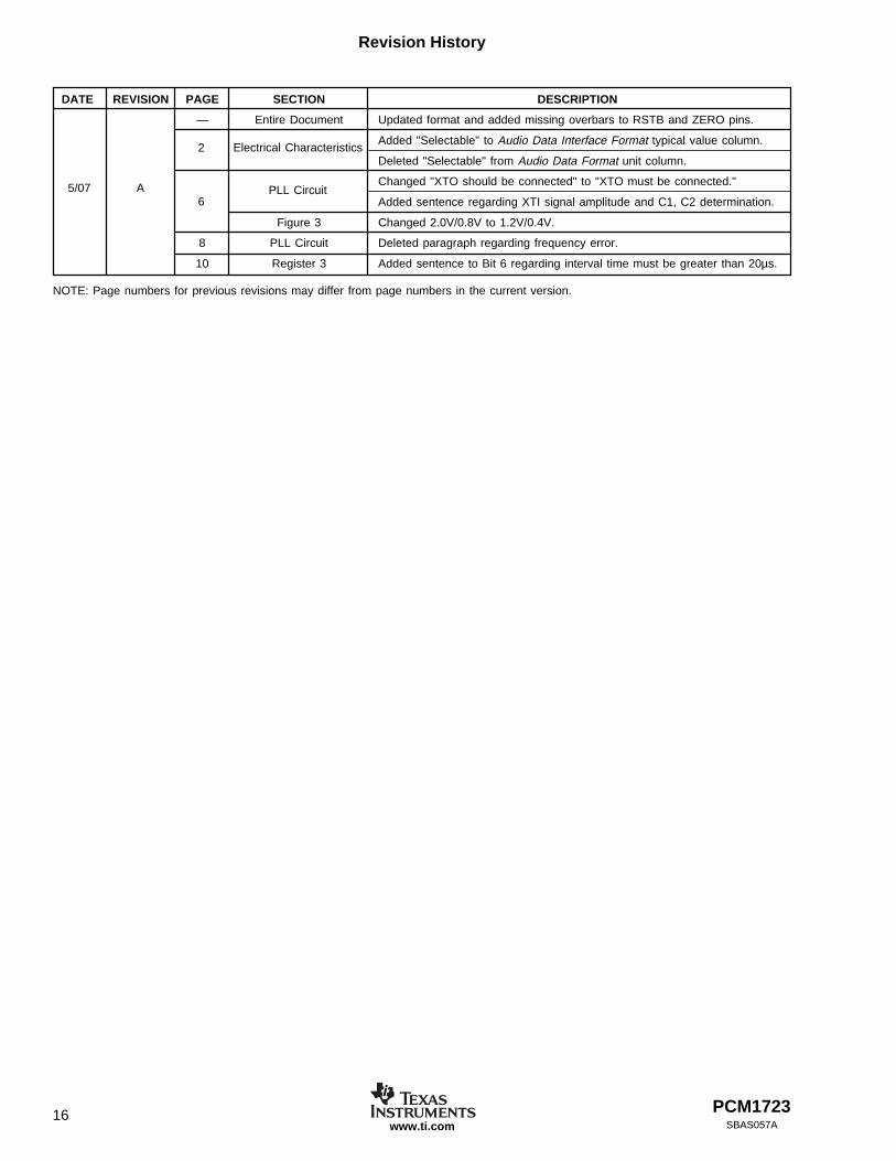
AC-3 APPLICATION CIRCUIT
A typical application for the PCM1723 is AC-3 5.1 channelaudio decoding and playback. This circuit uses the PCM1723to develop the audio system clock from the 27MHz videoclock, with the SCKO pin used to drive the AC-3 decoderand two PCM1720 units, the non-PLL version of thePCM1723.
FIGURE 17. Quantization Noise Spectrum.
3rd ORDER ∆Σ MODULATOR
Frequency (kHz)G
ain
(–dB
)
20
0
–20
–40
–60
–80
–100
–120
–140
–1600 5 10 15 20 25
FIGURE 16. 5-Level ∆Σ Modulator Block Diagram.
Out
48fS (384fS)64fS (256fS)
In
8fS18-Bit
+++
4
3
2
1
0
5-level Quantizer
+
–
+Z–1
+
–
+Z–1
++
Z–1
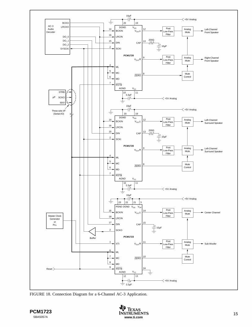
PCM1723 15SBAS057A www.ti.com
14
16
15
2
BCKO
LRCKO
DO_0
DO_1
DO_2
SYSCKI
BCKIN
LRCIN
DIN
SCKI
ML
MC
MD
RSTB
VOUTL
CAP
VOUTR
ZERO
Master ClockGenerator
orPLL
Reset
µP
STRB
SCKO
SDO
+5V Analog
PostLow-Pass
Filter
Three-wire I/F(Serial I/O) 3
20
PCM1720
PCM1720
PCM1723Buffer
19
DGNDAC-3Audio
Decoder
VDD
AGND VCC
4
5
6
7
9
8
12
13
AnalogMute
PostLow-Pass
Filter
AnalogMute
MuteControl
+5V Analog
10 11
14
16
15
2
BCKIN
LRCIN
DIN
SCKI
ML
MC
MD
RSTB
VOUTL
CAP
VOUTR
ZERO
+5V Analog
PostLow-Pass
Filter
10µF+
20 19
DGND VDD
AGND VCC
4
5
6
7
9
8
12
13
AnalogMute
PostLow-Pass
Filter
AnalogMute
Left-ChannelFront Speaker
Right-ChannelFront Speaker
Left-ChannelSurround Speaker
Left-ChannelSurround Speaker
Center Channel
Sub-Woofer
MuteControl
+5V Analog
10 11
16
18
17
BCKIN
LRCIN
DIN
SCKO
XTI
ML
MC
MD
VOUTL
CAP
VOUTR
ZERO
+5V Analog
PostLow-Pass
Filter
10µF+
2223 21 3
DGNDPGND VDD VDP
AGNDRSTB
VCC
6
7
8
9
11
10
14
15
2
1
AnalogMute
PostLow-Pass
Filter
AnalogMute
MuteControl
+5V Analog
12 13
24
+10µF
+3.3µF
+10µF
+
+
3.3µF
10µF
+3.3µF
200Ω
10µF+
200Ω
FIGURE 18. Connection Diagram for a 6-Channel AC-3 Application.
PCM172316SBAS057Awww.ti.com
DATE REVISION PAGE SECTION DESCRIPTION
— Entire Document Updated format and added missing overbars to RSTB and ZERO pins.
Added "Selectable" to Audio Data Interface Format typical value column.
Deleted "Selectable" from Audio Data Format unit column.
Changed "XTO should be connected" to "XTO must be connected."
Added sentence regarding XTI signal amplitude and C1, C2 determination.
Figure 3 Changed 2.0V/0.8V to 1.2V/0.4V.
8 PLL Circuit Deleted paragraph regarding frequency error.
10 Register 3 Added sentence to Bit 6 regarding interval time must be greater than 20µs.
Revision History
NOTE: Page numbers for previous revisions may differ from page numbers in the current version.
5/07 A
2 Electrical Characteristics
6PLL Circuit
PACKAGE OPTION ADDENDUM
www.ti.com 10-Dec-2020
Addendum-Page 1
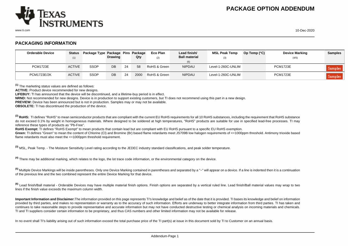
PACKAGING INFORMATION
Orderable Device Status(1)
Package Type PackageDrawing
Pins PackageQty
Eco Plan(2)
Lead finish/Ball material
(6)
MSL Peak Temp(3)
Op Temp (°C) Device Marking(4/5)
Samples
PCM1723E ACTIVE SSOP DB 24 58 RoHS & Green NIPDAU Level-1-260C-UNLIM PCM1723E
PCM1723E/2K ACTIVE SSOP DB 24 2000 RoHS & Green NIPDAU Level-1-260C-UNLIM PCM1723E
(1) The marketing status values are defined as follows:ACTIVE: Product device recommended for new designs.LIFEBUY: TI has announced that the device will be discontinued, and a lifetime-buy period is in effect.NRND: Not recommended for new designs. Device is in production to support existing customers, but TI does not recommend using this part in a new design.PREVIEW: Device has been announced but is not in production. Samples may or may not be available.OBSOLETE: TI has discontinued the production of the device.
(2) RoHS: TI defines "RoHS" to mean semiconductor products that are compliant with the current EU RoHS requirements for all 10 RoHS substances, including the requirement that RoHS substancedo not exceed 0.1% by weight in homogeneous materials. Where designed to be soldered at high temperatures, "RoHS" products are suitable for use in specified lead-free processes. TI mayreference these types of products as "Pb-Free".RoHS Exempt: TI defines "RoHS Exempt" to mean products that contain lead but are compliant with EU RoHS pursuant to a specific EU RoHS exemption.Green: TI defines "Green" to mean the content of Chlorine (Cl) and Bromine (Br) based flame retardants meet JS709B low halogen requirements of <=1000ppm threshold. Antimony trioxide basedflame retardants must also meet the <=1000ppm threshold requirement.
(3) MSL, Peak Temp. - The Moisture Sensitivity Level rating according to the JEDEC industry standard classifications, and peak solder temperature.
(4) There may be additional marking, which relates to the logo, the lot trace code information, or the environmental category on the device.
(5) Multiple Device Markings will be inside parentheses. Only one Device Marking contained in parentheses and separated by a "~" will appear on a device. If a line is indented then it is a continuationof the previous line and the two combined represent the entire Device Marking for that device.
(6) Lead finish/Ball material - Orderable Devices may have multiple material finish options. Finish options are separated by a vertical ruled line. Lead finish/Ball material values may wrap to twolines if the finish value exceeds the maximum column width.
Important Information and Disclaimer:The information provided on this page represents TI's knowledge and belief as of the date that it is provided. TI bases its knowledge and belief on informationprovided by third parties, and makes no representation or warranty as to the accuracy of such information. Efforts are underway to better integrate information from third parties. TI has taken andcontinues to take reasonable steps to provide representative and accurate information but may not have conducted destructive testing or chemical analysis on incoming materials and chemicals.TI and TI suppliers consider certain information to be proprietary, and thus CAS numbers and other limited information may not be available for release.
In no event shall TI's liability arising out of such information exceed the total purchase price of the TI part(s) at issue in this document sold by TI to Customer on an annual basis.
PACKAGE OPTION ADDENDUM
www.ti.com 10-Dec-2020
Addendum-Page 2
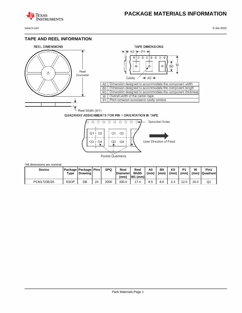
TAPE AND REEL INFORMATION
*All dimensions are nominal
Device PackageType
PackageDrawing
Pins SPQ ReelDiameter
(mm)
ReelWidth
W1 (mm)
A0(mm)
B0(mm)
K0(mm)
P1(mm)
W(mm)
Pin1Quadrant
PCM1723E/2K SSOP DB 24 2000 330.0 17.4 8.5 8.6 2.4 12.0 16.0 Q1
PACKAGE MATERIALS INFORMATION
www.ti.com 5-Jan-2022
Pack Materials-Page 1
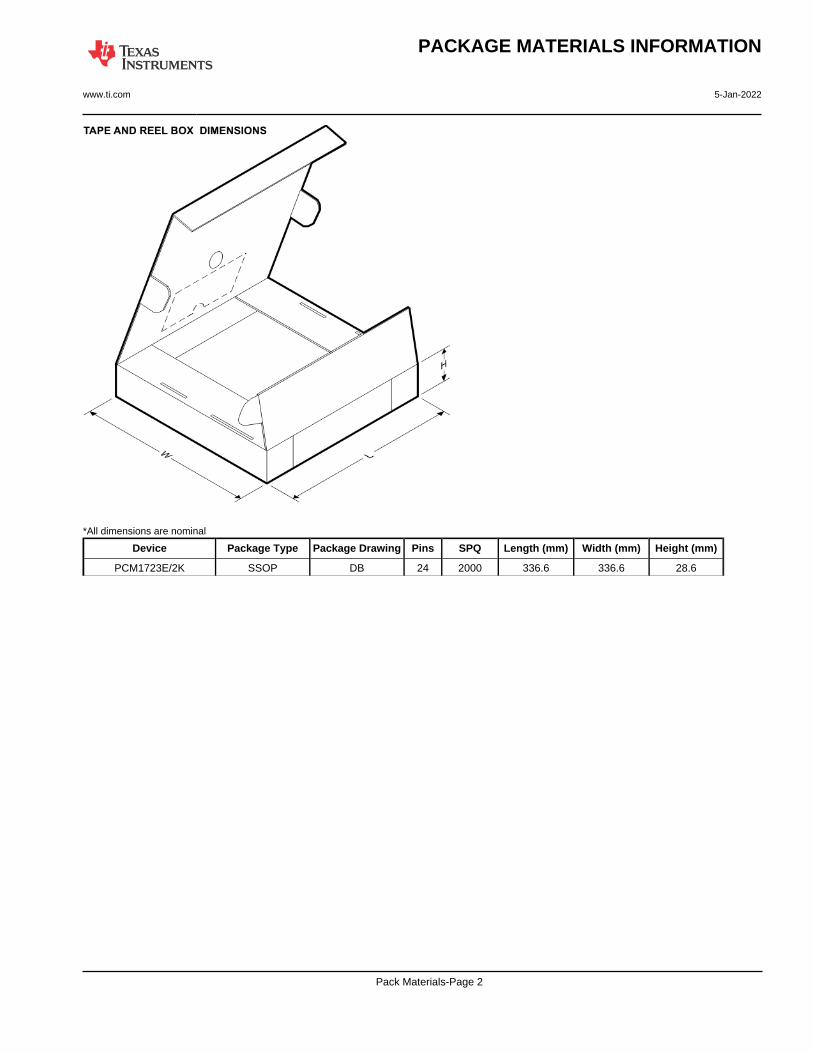
*All dimensions are nominal
Device Package Type Package Drawing Pins SPQ Length (mm) Width (mm) Height (mm)
PCM1723E/2K SSOP DB 24 2000 336.6 336.6 28.6
PACKAGE MATERIALS INFORMATION
www.ti.com 5-Jan-2022
Pack Materials-Page 2
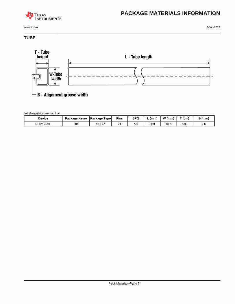
TUBE
*All dimensions are nominal
Device Package Name Package Type Pins SPQ L (mm) W (mm) T (µm) B (mm)
PCM1723E DB SSOP 24 58 500 10.6 500 9.6
PACKAGE MATERIALS INFORMATION
www.ti.com 5-Jan-2022
Pack Materials-Page 3
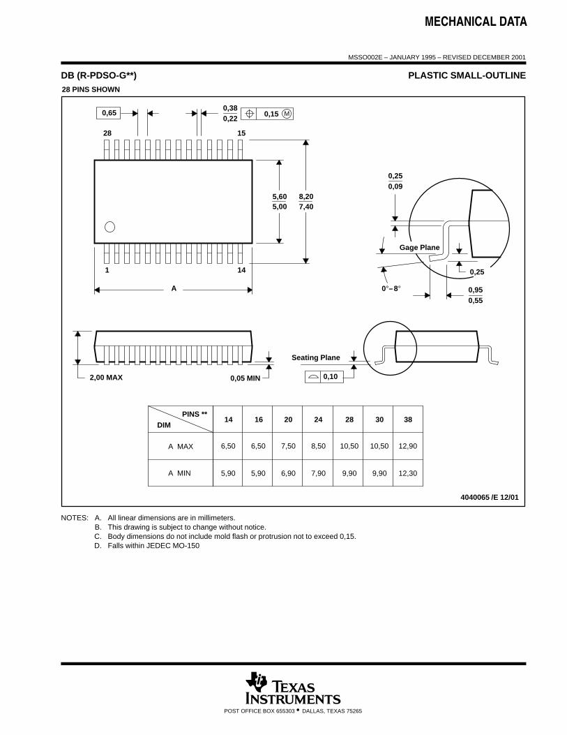
MECHANICAL DATA
MSSO002E – JANUARY 1995 – REVISED DECEMBER 2001
POST OFFICE BOX 655303 • DALLAS, TEXAS 75265
DB (R-PDSO-G**) PLASTIC SMALL-OUTLINE
4040065 /E 12/01
28 PINS SHOWN
Gage Plane
8,207,40
0,550,95
0,25
38
12,90
12,30
28
10,50
24
8,50
Seating Plane
9,907,90
30
10,50
9,90
0,38
5,605,00
15
0,22
14
A
28
1
2016
6,506,50
14
0,05 MIN
5,905,90
DIM
A MAX
A MIN
PINS **
2,00 MAX
6,90
7,50
0,65 M0,15
0°–8°
0,10
0,090,25
NOTES: A. All linear dimensions are in millimeters.B. This drawing is subject to change without notice.C. Body dimensions do not include mold flash or protrusion not to exceed 0,15.D. Falls within JEDEC MO-150
IMPORTANT NOTICE AND DISCLAIMERTI PROVIDES TECHNICAL AND RELIABILITY DATA (INCLUDING DATA SHEETS), DESIGN RESOURCES (INCLUDING REFERENCE DESIGNS), APPLICATION OR OTHER DESIGN ADVICE, WEB TOOLS, SAFETY INFORMATION, AND OTHER RESOURCES “AS IS” AND WITH ALL FAULTS, AND DISCLAIMS ALL WARRANTIES, EXPRESS AND IMPLIED, INCLUDING WITHOUT LIMITATION ANY IMPLIED WARRANTIES OF MERCHANTABILITY, FITNESS FOR A PARTICULAR PURPOSE OR NON-INFRINGEMENT OF THIRD PARTY INTELLECTUAL PROPERTY RIGHTS.These resources are intended for skilled developers designing with TI products. You are solely responsible for (1) selecting the appropriate TI products for your application, (2) designing, validating and testing your application, and (3) ensuring your application meets applicable standards, and any other safety, security, regulatory or other requirements.These resources are subject to change without notice. TI grants you permission to use these resources only for development of an application that uses the TI products described in the resource. Other reproduction and display of these resources is prohibited. No license is granted to any other TI intellectual property right or to any third party intellectual property right. TI disclaims responsibility for, and you will fully indemnify TI and its representatives against, any claims, damages, costs, losses, and liabilities arising out of your use of these resources.TI’s products are provided subject to TI’s Terms of Sale or other applicable terms available either on ti.com or provided in conjunction with such TI products. TI’s provision of these resources does not expand or otherwise alter TI’s applicable warranties or warranty disclaimers for TI products.TI objects to and rejects any additional or different terms you may have proposed. IMPORTANT NOTICE
Mailing Address: Texas Instruments, Post Office Box 655303, Dallas, Texas 75265Copyright © 2022, Texas Instruments Incorporated
Related Documents