5 5 4 4 3 3 2 2 1 1 D D C C B B A A NOTES, UNLESS OTHERWISE SPECIFIED: REVISIONS COMPUTER GENERATED DRAWING - DO NOT REVISE MANUALLY APPROVED DATE DESCRIPTION REV ECO 2149913: Initial Release A Sheet 1: Cover Sheet 2: Block Diagram Sheet 3: FPGA Front End I/F Sheet 4: FPGA DDR3 I/F Sheet 5: DDR3 Memory 1&2 Sheet 6: DDR3 Memory 3&4 Sheet 7: FPGA Video Out I/F Sheet 8: FPGA Programming/Test MUX Sheet 9: FPGA Power Sheet 10: FPGA Regulators Sheet 11: FPGA Regulators Sheet 12: FPGA Ground Sheet 13: ASIC Video Input I/F Sheet 14: Master DMD Flex I/F Sheet 15: Slave DMD Flex I/F Sheet 16: Input Power and PMD1000 I/F Sheet 17: Primary PMD1000 Power Supplies Sheet 18: Secondary PMD1000 Power Supplies Sheet 19: ColorWheel Drive Sheet 20: Fans, CW Index, Peripheral Connectors Sheet 21: Master ASIC GPIO, I2C, and Lamp Ballast Sheet 22: GPIO Expander, Keypad Interface and IR Sheet 23: Master ASIC TP, ARM JTAG, RESET Sheet 24: Slave ASIC TP, ARM JTAG Sheet 25: Master RS-232. SPI, and USB Sheet 26: Master ASIC Flash I/F Sheet 27: Slave ASIC Flash I/F Sheet 28: ASIC SSI I/F Sheet 29: SSI Driver I/F Sheet 30: Slave ASIC GPIO & Smooth Picture I/F Sheet 31: Smooth Picture Electronics Sheet 32: Master Power and Bypass Caps Sheet 33: Slave Power and Bypass Caps Sheet 34: Revisions INDEX 4/13/2015 DH ECO 2150627 B 5/15/2015 DH 1. The netname "P1P1V" represents connection to the +1.1V FPGA power plane 2. The netname "P1P1V_FIL" represents connection to the +1.1V filtered FPGA power plane 3. The netname "P1P1V_M" represents connection to the +1.1V Master ASIC power plane 4. The netname "P1P1V_S" represents connection to the +1.1V Slave ASIC power plane 5. The netname "P1P15V" represents connection to the +1.15V FPGA power plane 6. The netname "P1P15V" represents connection to the +1.15V filtered FPGA power plane 7. The netname "P1P5V" represents connection to the +1.5V FPGA power plane 8. The netname "P1P5V_FIL" represents connection to the +1.5V filtered FPGA power plane 9. The netname "P1P8V_M" represents connection to the +1.8V Master ASIC power plane 10. The netname "P1P8V_S" represents connection to the +1.8V Slave ASIC power plane 11. The netname "A1P8V_M" represents connection to the +1.8V Master ASIC power plane for the PLLs 12. The netname "A1P8V_S" represents connection to the +1.8V Slave ASIC power plane for the PLLs 13. The netname "P2P5V" represents connection to the +2.5V FPGA power plane 14. The netname "P2P5V_FIL" represents connection to the +2.5V filtered FPGA power plane 15. The netname "P2P5V_M" represents connection to the +2.5V Master ASIC power plane 16. The netname "P2P5V_S" represents connection to the +2.5V Slave ASIC power plane 17. The netname "P3P3V" represents connection to the +3.3V FPGA power plane 18. The netname "P3P3V_M" represents connection to the +3.3V Master ASIC power plane 19. The netname "P3P3V_S" represents connection to the +3.3V Slave ASIC power plane 20. The netname "P5V_M" represents connection to the +5V Master ASIC power plane 21. The netname "P5V_S" represents connection to the +5V Slave ASIC power plane 22. The netname "P12V" represents the connection to the +12.0V power plane. 23. The netname "GND" represents connection to the ground plane 24. A "Z" suffix on a signal name indicates an active low signal 25. All components with designators "U*", "Q*", "D*" are electrostactic discharge sensitive. 26. All components with designators above 500 are mounted on the bottom side of the board. 27. All resistor values are in ohms. ECO 2150877 C 6/25/2015 DH ECO 2153403 D 9/15/2015 DH TEXAS INSTRUMENTS (C) COPYRIGHT 2015 TEXAS INSTRUMENTS ALL RIGHTS RESERVED TITLE DRAWING NO REV SCALE SHEET of DWN ENGR APVD MFG QA SW DATE NEXT ASSY USED ON APPLICATION A3 E 2514423 TIDA-01347 P66 4KUHD Formatter Board 34 1 Ben Uhing Cadence 16.6 9/30/2016 Scott Vestal 4/9/2015 TEXAS INSTRUMENTS (C) COPYRIGHT 2015 TEXAS INSTRUMENTS ALL RIGHTS RESERVED TITLE DRAWING NO REV SCALE SHEET of DWN ENGR APVD MFG QA SW DATE NEXT ASSY USED ON APPLICATION A3 E 2514423 TIDA-01347 P66 4KUHD Formatter Board 34 1 Ben Uhing Cadence 16.6 9/30/2016 Scott Vestal 4/9/2015 TEXAS INSTRUMENTS (C) COPYRIGHT 2015 TEXAS INSTRUMENTS ALL RIGHTS RESERVED TITLE DRAWING NO REV SCALE SHEET of DWN ENGR APVD MFG QA SW DATE NEXT ASSY USED ON APPLICATION A3 E 2514423 TIDA-01347 P66 4KUHD Formatter Board 34 1 Ben Uhing Cadence 16.6 9/30/2016 Scott Vestal 4/9/2015

Welcome message from author
This document is posted to help you gain knowledge. Please leave a comment to let me know what you think about it! Share it to your friends and learn new things together.
Transcript

5
5
4
4
3
3
2
2
1
1
D D
C C
B B
A A
NOTES, UNLESS OTHERWISE SPECIFIED:REVISIONS
COMPUTER GENERATED DRAWING - DO NOT REVISE MANUALLY
APPROVEDDATEDESCRIPTIONREV
ECO 2149913: Initial ReleaseA
Sheet 1: CoverSheet 2: Block DiagramSheet 3: FPGA Front End I/FSheet 4: FPGA DDR3 I/FSheet 5: DDR3 Memory 1&2Sheet 6: DDR3 Memory 3&4Sheet 7: FPGA Video Out I/FSheet 8: FPGA Programming/Test MUXSheet 9: FPGA PowerSheet 10: FPGA RegulatorsSheet 11: FPGA RegulatorsSheet 12: FPGA GroundSheet 13: ASIC Video Input I/FSheet 14: Master DMD Flex I/FSheet 15: Slave DMD Flex I/FSheet 16: Input Power and PMD1000 I/FSheet 17: Primary PMD1000 Power SuppliesSheet 18: Secondary PMD1000 Power SuppliesSheet 19: ColorWheel DriveSheet 20: Fans, CW Index, Peripheral ConnectorsSheet 21: Master ASIC GPIO, I2C, and Lamp BallastSheet 22: GPIO Expander, Keypad Interface and IR Sheet 23: Master ASIC TP, ARM JTAG, RESETSheet 24: Slave ASIC TP, ARM JTAGSheet 25: Master RS-232. SPI, and USBSheet 26: Master ASIC Flash I/FSheet 27: Slave ASIC Flash I/FSheet 28: ASIC SSI I/FSheet 29: SSI Driver I/FSheet 30: Slave ASIC GPIO & Smooth Picture I/FSheet 31: Smooth Picture ElectronicsSheet 32: Master Power and Bypass CapsSheet 33: Slave Power and Bypass CapsSheet 34: Revisions
INDEX
4/13/2015 DH
ECO 2150627B 5/15/2015 DH
1. The netname "P1P1V" represents connection to the +1.1V FPGA power plane2. The netname "P1P1V_FIL" represents connection to the +1.1V filtered FPGA power plane3. The netname "P1P1V_M" represents connection to the +1.1V Master ASIC power plane4. The netname "P1P1V_S" represents connection to the +1.1V Slave ASIC power plane5. The netname "P1P15V" represents connection to the +1.15V FPGA power plane6. The netname "P1P15V" represents connection to the +1.15V filtered FPGA power plane7. The netname "P1P5V" represents connection to the +1.5V FPGA power plane8. The netname "P1P5V_FIL" represents connection to the +1.5V filtered FPGA power plane9. The netname "P1P8V_M" represents connection to the +1.8V Master ASIC power plane10. The netname "P1P8V_S" represents connection to the +1.8V Slave ASIC power plane11. The netname "A1P8V_M" represents connection to the +1.8V Master ASIC power plane for the PLLs12. The netname "A1P8V_S" represents connection to the +1.8V Slave ASIC power plane for the PLLs13. The netname "P2P5V" represents connection to the +2.5V FPGA power plane14. The netname "P2P5V_FIL" represents connection to the +2.5V filtered FPGA power plane15. The netname "P2P5V_M" represents connection to the +2.5V Master ASIC power plane16. The netname "P2P5V_S" represents connection to the +2.5V Slave ASIC power plane17. The netname "P3P3V" represents connection to the +3.3V FPGA power plane18. The netname "P3P3V_M" represents connection to the +3.3V Master ASIC power plane19. The netname "P3P3V_S" represents connection to the +3.3V Slave ASIC power plane20. The netname "P5V_M" represents connection to the +5V Master ASIC power plane21. The netname "P5V_S" represents connection to the +5V Slave ASIC power plane22. The netname "P12V" represents the connection to the +12.0V power plane.23. The netname "GND" represents connection to the ground plane24. A "Z" suffix on a signal name indicates an active low signal25. All components with designators "U*", "Q*", "D*" are electrostactic discharge sensitive.26. All components with designators above 500 are mounted on the bottom side of the board.27. All resistor values are in ohms.
ECO 2150877C 6/25/2015 DH
ECO 2153403D 9/15/2015 DH
TEXAS INSTRUMENTS
(C) COPYRIGHT 2015 TEXAS INSTRUMENTSALL RIGHTS RESERVED
TITLE
DRAWING NO REV
SCALE SHEET of
DWN
ENGR
APVD
MFG
QA
SW
DATE
NEXT ASSY USED ON
APPLICATION
A3 E2514423
TIDA-01347 P66 4KUHD Formatter Board
341
Ben Uhing
Cadence 16.6
9/30/2016
Scott Vestal 4/9/2015TEXAS INSTRUMENTS
(C) COPYRIGHT 2015 TEXAS INSTRUMENTSALL RIGHTS RESERVED
TITLE
DRAWING NO REV
SCALE SHEET of
DWN
ENGR
APVD
MFG
QA
SW
DATE
NEXT ASSY USED ON
APPLICATION
A3 E2514423
TIDA-01347 P66 4KUHD Formatter Board
341
Ben Uhing
Cadence 16.6
9/30/2016
Scott Vestal 4/9/2015TEXAS INSTRUMENTS
(C) COPYRIGHT 2015 TEXAS INSTRUMENTSALL RIGHTS RESERVED
TITLE
DRAWING NO REV
SCALE SHEET of
DWN
ENGR
APVD
MFG
QA
SW
DATE
NEXT ASSY USED ON
APPLICATION
A3 E2514423
TIDA-01347 P66 4KUHD Formatter Board
341
Ben Uhing
Cadence 16.6
9/30/2016
Scott Vestal 4/9/2015
5
5
4
4
3
3
2
2
1
1
D D
C C
B B
A A
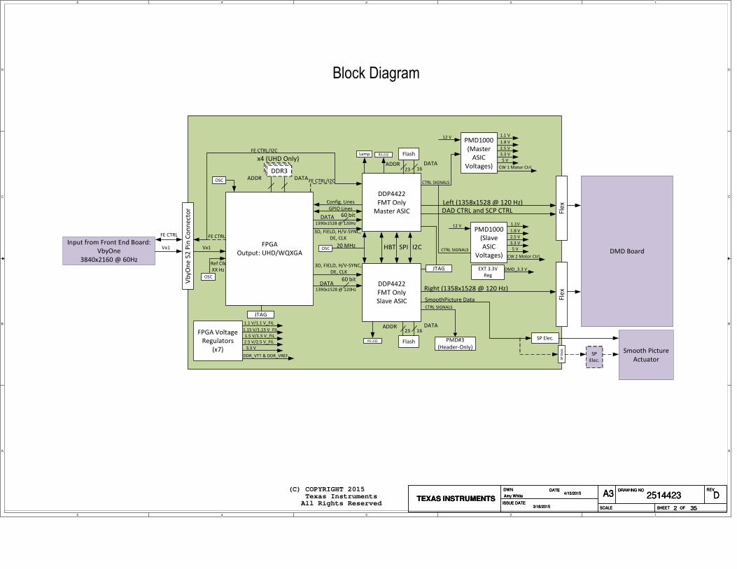
Vb
yO
ne
52
Pin
Co
nn
ect
or
FPGA
Output: UHD/WQXGA
DDP4422
FMT Only
Master ASIC
DDP4422
FMT Only
Slave ASIC
Fle
xFle
x
Input from Front End Board:
VbyOne
3840x2160 @ 60Hz
DMD Board
Left (1358x1528 @ 120 Hz)
Right (1358x1528 @ 120 Hz)1390x1528 @ 120Hz
Smooth Picture
Actuator
SPI
60 bit
60 bit
DAD CTRL and SCP CTRL
PMD1000
(Master
ASIC
Voltages)
1.1 V
1.8 V
2.5 V
3.3 V
5 V
CW 1 Motor Ctrl
12 V
CTRL SIGNALS
DDR3DDR3DDR3ADDR DATA
x4 (UHD Only)
JTAG
HBT
Flash
Flash
ADDR DATA
DATAADDR
Config. Lines
I2C
FE CTRL/I2C
GPIO Lines
DATA
DATA
FE CTRL
FE CTRL/I2C
FE CTRL
SP Elec.
1390x1528 @ 120Hz
3D, FIELD, H/V-SYNC,
DE, CLK
SP
Da
ta
PMD1000
(Slave
ASIC
Voltages)
1.1V
1.8 V
2.5 V
3.3 V
5 V
CW 2 Motor Ctrl
12 V
SP
Elec.
16
1623
23
SmoothPicture Data
3D, FIELD, H/V-SYNC,
DE, CLKJTAG
CTRL SIGNALSVx1 Vx1
PMD#3
(Header-Only)
CTRL SIGNALS
FPGA Voltage
Regulators
(x7)
1.1 V/1.1 V_FIL
1.15 V/1.15 V_FIL
1.5 V/1.5 V_FIL
2.5 V/2.5 V_FIL
3.3 V
DDR_VTT & DDR_VREF
EXT 3.3V
Reg
DMD_3.3 V
OSC20 MHz
OSC
OSC
Ref Clk
XX Hz
RS-232
RS-232Lamp
(C) COPYRIGHT 2015 Texas Instruments All Rights Reserved
Block Diagram
TEXAS INSTRUMENTS
DWN DATE
ISSUE DATE
SCALE
DRAWING NO REV
SHEET OF
2514423 DA3
352
Amy White4/13/2015
3/18/2015
TEXAS INSTRUMENTS
DWN DATE
ISSUE DATE
SCALE
DRAWING NO REV
SHEET OF
2514423 DA3
352
Amy White4/13/2015
3/18/2015
TEXAS INSTRUMENTS
DWN DATE
ISSUE DATE
SCALE
DRAWING NO REV
SHEET OF
2514423 DA3
352
Amy White4/13/2015
3/18/2015
5
5
4
4
3
3
2
2
1
1
D D
C C
B B
A A
(C) COPYRIGHT 2015 Texas Instruments All Rights Reserved
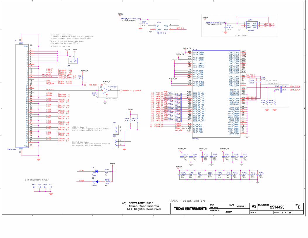
FPGA - Front-End I/F
CCA MOUNTING HOLES
Note: J503 - Input PowerIf front-end board can supply 12V with sufficent current to power formatter board install J503.
DO NOT INSTALL J503 while input power from wall plug is in use (J27).
Default: Not Installed
J505 Vx1 Swap PNInstalled: Not Swapping P and N's (Default)Not Installed: Swapping P and N's
J506 Vx1 Swap OrderInstalled: Not Bit Order Swapping (Default)Not Installed: Bit Order Swapping
Do Not Install
Do Not Install
Do Not Install
Do Not InstallP3P3V_M
P3P3V_M
FE_12V P12V
P3P3V
P2P5V_FIL
P1P5V_FIL
P1P15V
P1P15V_FIL
P3P3V
P2P5V_FIL P1P5V_FIL P1P15V_FIL
P1P15V
P3P3V
P3P3V
PWRGOOD p.16,23,26
I2C_BUSY p.21
HTPDN p.3LOCKN p.3
RX0N p.3RX0P p.3
RX1N p.3RX1P p.3
RX2N p.3RX2P p.3
RX3N p.3RX3P p.3
RX4N p.3RX4P p.3
RX5N p.3RX5P p.3
RX6N p.3RX6P p.3
RX7N p.3RX7P p.3
RX0Np.3RX0Pp.3RX1Np.3RX1Pp.3RX2Np.3RX2Pp.3RX3Np.3RX3Pp.3RX4Np.3RX4Pp.3RX5Np.3RX5Pp.3RX6Np.3RX6Pp.3RX7Np.3RX7Pp.3
LOCKNp.3HTPDNp.3
USB+5V p.25USB_D+ p.25USB_D- p.25
SCL0 p.21,22SDA0 p.21,22
VX1_LR_SYNC p.8VX1_3D_EN p.8
TEXAS INSTRUMENTS
DWN DATE
ISSUE DATE
SCALE
DRAWING NO REV
SHEET OF
2514423 EA3
343
Ben Uhing9/30/2016
1/31/2017
TEXAS INSTRUMENTS
DWN DATE
ISSUE DATE
SCALE
DRAWING NO REV
SHEET OF
2514423 EA3
343
Ben Uhing9/30/2016
1/31/2017
TEXAS INSTRUMENTS
DWN DATE
ISSUE DATE
SCALE
DRAWING NO REV
SHEET OF
2514423 EA3
343
Ben Uhing9/30/2016
1/31/2017
R231K
MT2
C360.1 uF
C310.1 uF
C549
0.1 uF
C5740.1 uF10V10%
C529100 uF6.3V20%
R53849.9
1%
C400.1 uF
MT4
U506
75.000 MHz
EN1
GND2
OUT3
VCC4
C57210 nF25V10%
C350.1 uF
C300.1 uF
C545
0.1 uF
C547 0.1 uF
J9
FI-RE51S-HF
11
22
33
44
55
66
77
88
99
1010
1111
1212
1313
1414
1515
1616
1717
1818
1919
2020
2121
2222
2323
2424
2525
2626
2727
2828
2929
3030
3131
3232
3333
3434
3535
3636
3737
3838
3939
4040
4141
4242
4343
4444
4545
4646
4747
4848
4949
5050
5151
GND52
53
GND
GND54
55
GND
C390.1 uF
C340.1 uF
C290.1 uF
C56410 nF25V10%
C440.1 uF
C380.1 uF
C330.1 uF
C73310 nF25V10%
U13H
XPR3821
GXB_RX_L0NAD29
GXB_RX_L0PAD30
GXB_RX_L1NAB29
GXB_RX_L1PAB30
GXB_RX_L2NY29
GXB_RX_L2PY30
GXB_RX_L3NV29
GXB_RX_L3PV30
GXB_RX_L4NT29
GXB_RX_L4PT30
GXB_RX_L5NP29
GXB_RX_L5PP30
GXB_RX_L6NM29
GXB_RX_L6PM30
GXB_RX_L7NK29
GXB_RX_L7PK30
GXB_RX_L8NH29
GXB_RX_L8PH30
GXB_TX_L0NAC27
GXB_TX_L0PAC28
GXB_TX_L1NAA27
GXB_TX_L1PAA28
GXB_TX_L2NW27
GXB_TX_L2PW28
GXB_TX_L3NU27
GXB_TX_L3PU28
GXB_TX_L4NR27
GXB_TX_L4PR28
GXB_TX_L5NN27
GXB_TX_L5PN28
GXB_TX_L6NL27
GXB_TX_L6PL28
GXB_TX_L7NJ27
GXB_TX_L7PJ28
GXB_TX_L8NG27
GXB_TX_L8PG28
REFCLK2LNR23REFCLK2LPR22
REFCLK1LNU23
REFCLK1LPU22
REFCLK0LNW23
REFCLK0LPW22
VCCA_GXBL0V24
VCCA_GXBL1P24
VCCH_GXBL0T24
VCCH_GXBL1N25
VCCL_GXBL0T25
VCCL_GXBL0T26
VCCL_GXBL1M25
VCCR_GXBLM26
VCCR_GXBLR25
VCCR_GXBLR26
VCCR_GXBLW25
VCCR_GXBLW26
VCCT_GXBL0U25
VCCT_GXBL0V26
VCCT_GXBL1P26
IO_4A_AB7AB7 IO_4A_AB6AB6
VCCR_GXBRM5VCCL_GXBR1M6VCCL_GXBR1N6VCCH_GXBR1N7VCCT_GXBR1P5VCCA_GXBR1P7VCCT_GXBR1R6VCCR_GXBRT5VCCR_GXBRT6VCCH_GXBR0T7VCCL_GXBR0U6VCCT_GXBR0V5VCCA_GXBR0V7VCCR_GXBRW5VCCR_GXBRW6
IO_4A_AE7AE7 IO_4A_AD7AD7
IO_3A_AG27AG27
U504
135 MHz
OE1
NC2
GND3
OUT4OUTz5VCC6
C370.1 uF
C56510 nF25V10%
C420.1 uF
C546 0.1 uF
J32
1
2
C54310uF6.3V20%
R5091K
C69110 nF25V10%
R511
100
5%
C410.1 uF
C57710 nF25V10%
MT1
FB502 470 OhmBLM18AG471SN1D
C5340.01 uF10%
J33
1
2
C55810 nF25V10%
C430.1 uF
C5710.22 uF
6.3V
U5 74LVC1G07
2 4
5
13
C5240.01 uF10%
C64310 nF25V10%
D1
Green
C57510 nF25V10%
C5610.22 uF
6.3V
R12110K
C60910 nF25V10%
D2
Green
R510
100
5%
FB500 470 OhmBLM18AG471SN1D
J11
12
MT3
R12010K
C56210 nF25V10%
C5600.1 uF10V10%
C320.1 uF
R53949.9
1%
I2C_BUSY
RX7PRX7N
RX6PRX6N
RX5PRX5N
RX4PRX4N
RX3PRX3N
RX2PRX2N
RX1PRX1N
RX0PRX0N
LOCKNHTPDN
SDA0SCL0
USB_D-USB_D+USB+5V
FE_RSTZ
RX7PRX7NRX6PRX6NRX5PRX5NRX4PRX4NRX3PRX3NRX2PRX2NRX1PRX1NRX0PRX0N
LOCKNHTPDNSWAP_PNSWAP_ORDER
Test_TX8_N
TEST_RX8_N
Test_TX8_P
TEST_RX8_P
LOCKN
HTPDN
REF_CLK
REF_CLK
VBY1_CLK_P
VBY1_CLK_P
VBY1_CLK_N
VBY1_CLK_N
VX1_3D_ENVX1_LR_SYNC
5
5
4
4
3
3
2
2
1
1
D D
C C
B B
A A
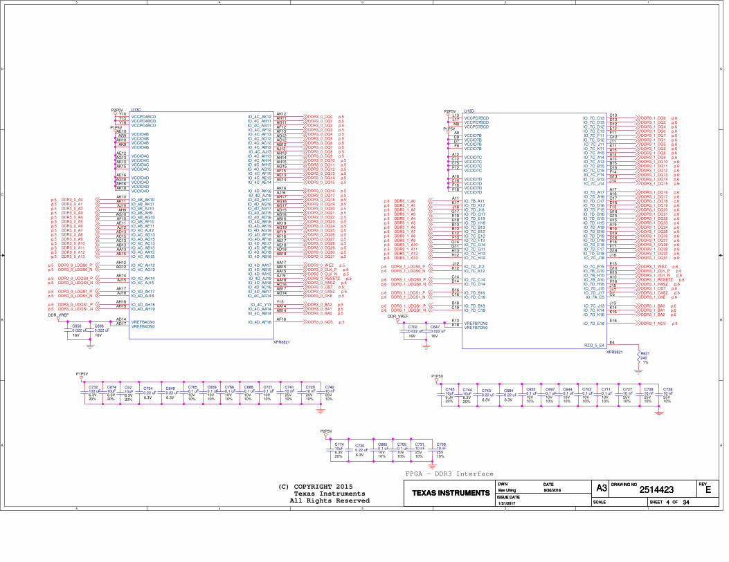
FPGA - DDR3 Interface
(C) COPYRIGHT 2015 Texas Instruments All Rights Reserved
P2P5V
P1P5V
P2P5V
P1P5V
P2P5V
P1P5VP1P5V
DDR_VREFDDR_VREF
DDR3_0_A0p.5DDR3_0_A1p.5DDR3_0_A2p.5DDR3_0_A3p.5DDR3_0_A4p.5DDR3_0_A5p.5DDR3_0_A6p.5DDR3_0_A7p.5DDR3_0_A8p.5DDR3_0_A9p.5DDR3_0_A10p.5DDR3_0_A11p.5DDR3_0_A12p.5DDR3_0_A13p.5
DDR3_0_LDQS0_Np.5DDR3_0_LDQS0_Pp.5
DDR3_0_UDQS0_Np.5DDR3_0_UDQS0_Pp.5
DDR3_0_LDQS1_Np.5DDR3_0_LDQS1_Pp.5
DDR3_0_UDQS1_Np.5DDR3_0_UDQS1_Pp.5
DDR3_0_WEZ p.5DDR3_0_CLK_P p.5DDR3_0_CLK_N p.5DDR3_0_RESETZ p.5DDR3_0_RASZ p.5DDR3_0_ODT p.5DDR3_0_CASZ p.5
DDR3_0_DQ0 p.5DDR3_0_DQ1 p.5DDR3_0_DQ2 p.5DDR3_0_DQ3 p.5DDR3_0_DQ4 p.5DDR3_0_DQ5 p.5DDR3_0_DQ6 p.5DDR3_0_DQ7 p.5DDR3_0_DQ8 p.5DDR3_0_DQ9 p.5DDR3_0_DQ10 p.5DDR3_0_DQ11 p.5DDR3_0_DQ12 p.5DDR3_0_DQ13 p.5DDR3_0_DQ14 p.5DDR3_0_DQ15 p.5
DDR3_0_DQ16 p.5DDR3_0_DQ17 p.5DDR3_0_DQ18 p.5DDR3_0_DQ19 p.5DDR3_0_DQ20 p.5DDR3_0_DQ21 p.5DDR3_0_DQ22 p.5DDR3_0_DQ23 p.5DDR3_0_DQ24 p.5DDR3_0_DQ25 p.5DDR3_0_DQ26 p.5DDR3_0_DQ27 p.5DDR3_0_DQ28 p.5DDR3_0_DQ29 p.5DDR3_0_DQ30 p.5DDR3_0_DQ31 p.5
DDR3_1_A0p.6DDR3_1_A1p.6DDR3_1_A2p.6DDR3_1_A3p.6DDR3_1_A4p.6DDR3_1_A5p.6DDR3_1_A6p.6DDR3_1_A7p.6DDR3_1_A8p.6DDR3_1_A9p.6DDR3_1_A10p.6DDR3_1_A11p.6DDR3_1_A12p.6DDR3_1_A13p.6
DDR3_1_LDQS0_Np.6DDR3_1_LDQS0_Pp.6
DDR3_1_UDQS0_Np.6DDR3_1_UDQS0_Pp.6
DDR3_1_LDQS1_Np.6DDR3_1_LDQS1_Pp.6
DDR3_1_UDQS1_Np.6DDR3_1_UDQS1_Pp.6
DDR3_1_WEZ p.6DDR3_1_CLK_P p.6DDR3_1_CLK_N p.6DDR3_1_RESETZ p.6DDR3_1_RASZ p.6DDR3_1_ODT p.6DDR3_1_CASZ p.6
DDR3_1_DQ8 p.6DDR3_1_DQ9 p.6DDR3_1_DQ10 p.6DDR3_1_DQ11 p.6DDR3_1_DQ12 p.6DDR3_1_DQ13 p.6DDR3_1_DQ14 p.6DDR3_1_DQ15 p.6
DDR3_1_DQ16 p.6DDR3_1_DQ17 p.6DDR3_1_DQ18 p.6DDR3_1_DQ19 p.6DDR3_1_DQ20 p.6DDR3_1_DQ21 p.6DDR3_1_DQ22 p.6DDR3_1_DQ23 p.6DDR3_1_DQ24 p.6DDR3_1_DQ25 p.6DDR3_1_DQ26 p.6DDR3_1_DQ27 p.6DDR3_1_DQ28 p.6DDR3_1_DQ29 p.6DDR3_1_DQ30 p.6DDR3_1_DQ31 p.6
DDR3_0_BA2 p.5DDR3_0_BA1 p.5DDR3_0_BA0 p.5
DDR3_1_BA1 p.6
DDR3_0_NCS p.5 DDR3_1_NCS p.6
DDR3_0_CKE p.5 DDR3_1_CKE p.6
DDR3_1_BA2 p.6
DDR3_1_BA0 p.6
DDR3_1_DQ0 p.6
DDR3_1_DQ1 p.6
DDR3_1_DQ2 p.6
DDR3_1_DQ3 p.6
DDR3_1_DQ4 p.6
DDR3_1_DQ5 p.6
DDR3_1_DQ6 p.6
DDR3_1_DQ7 p.6
TEXAS INSTRUMENTS
DWN DATE
ISSUE DATE
SCALE
DRAWING NO REV
SHEET OF
2514423 EA3
344
Ben Uhing 9/30/2016
1/31/2017
TEXAS INSTRUMENTS
DWN DATE
ISSUE DATE
SCALE
DRAWING NO REV
SHEET OF
2514423 EA3
344
Ben Uhing 9/30/2016
1/31/2017
TEXAS INSTRUMENTS
DWN DATE
ISSUE DATE
SCALE
DRAWING NO REV
SHEET OF
2514423 EA3
344
Ben Uhing 9/30/2016
1/31/2017
C5710uF6.3V20%
C6650.1 uF10V10%
C6550.1 uF10V10%
C72710 nF25V10%
C7050.1 uF10V10%
R621240
1%
U13C
XPR3821
IO_4B_AE11AE11
IO_4B_AK11AK11 IO_4B_AK10AK10
IO_4B_AF10AF10 IO_4B_AG10AG10 IO_4B_AH9
AH9 IO_4B_AJ10AJ10
IO_4C_AA14AA14
IO_4C_AB14AB14
IO_4C_AG15AG15IO_4C_AH15AH15
IO_4C_AE15AE15
IO_4C_AF15AF15
IO_4C_AJ15AJ15 IO_4C_AK14AK14
IO_4C_AH14AH14
IO_4C_AD13AD13
IO_4C_AE13AE13
IO_4C_AE14AE14
IO_4C_AH13AH13IO_4C_AJ13AJ13
IO_4C_AC13AC13
IO_4C_AD12AD12
IO_4C_AF12AF12
IO_4C_AF13AF13
IO_4C_AA13AA13 IO_4C_AB13AB13
IO_4C_AG12AG12 IO_4C_AH12AH12
IO_4C_AJ12AJ12
IO_4C_AK12AK12
IO_4C_AB12AB12IO_4C_AC12AC12
IO_4C_Y13Y13
IO_4C_AG11AG11IO_4C_AH11AH11
IO_4D_AJ19AJ19
IO_4D_AK19AK19
IO_4D_AF19AF19IO_4D_AG19AG19
IO_4D_AD18AD18
IO_4D_AH19AH19 IO_4D_AH18AH18
IO_4D_AA18AA18
IO_4D_AB18AB18
IO_4D_AE18AE18
IO_4D_AF18AF18
IO_4D_AE17AE17
IO_4D_AA17AA17
IO_4D_AB17AB17
IO_4D_AB16AB16
IO_4D_AG17AG17
IO_4D_AH17AH17
IO_4D_AC16AC16
IO_4D_AD16AD16
IO_4D_AJ18AJ18 IO_4D_AK17AK17
IO_4D_AG16AG16
IO_4D_AB15AB15
IO_4D_AC15AC15
IO_4D_AD15AD15
IO_4D_AJ16AJ16IO_4D_AK16AK16
VCCIO4BAE10
VCCIO4BAG9
VCCIO4BAH10
VCCIO4BAK9
VCCIO4CAE12
VCCIO4CAG13
VCCIO4CAK13
VCCIO4CAK15
VCCIO4DAE16
VCCIO4DAG18
VCCIO4DAH16
VCCIO4DAK18
VCCPD4BCDY10
VCCPD4BCDY15
VCCPD4BCDY18
IO_4C_AG14AG14
IO_4D_AA15AA15
VREFB4DN0AD17 IO_4D_AF16
AF16VREFB4CN0
AD14
C732100 uF6.3V20%
C6970.1 uF10V10%
C72810 nF25V10%
C74510uF6.3V20%
C73910 nF25V10%
C67410uF6.3V20%
C72910 nF25V10%
C7650.1 uF10V10%
C73110 nF25V10%
C6470.022 uF
16V
C6440.1 uF10V10%
C6490.22 uF
6.3V
C6590.1 uF10V10%
C74410uF6.3V20%
C7020.022 uF
16V
C74110 nF25V10%
C7540.22 uF
6.3V
C6840.22 uF
6.3V
C7030.1 uF10V10%
C72010 nF25V10%
C6980.022 uF
16V
C7430.22 uF
6.3V
C77410uF6.3V20%
C7660.1 uF10V10%
C74210 nF25V10%
C6560.022 uF
16V
C7110.1 uF10V10%
C7300.22 uF
6.3V
C7210.1 uF10V10%
U13D
XPR3821
IO_7B_A11A11
IO_7B_A10A10
IO_7C_J11J11
IO_7C_K11K11
IO_7C_F11F11
IO_7C_G11G11
IO_7C_B13B13
IO_7C_B12B12
IO_7C_D12D12
IO_7C_E12E12
IO_7C_J12J12
IO_7C_K12K12
IO_7C_G12G12
IO_7C_H12H12
IO_7C_C13C13
IO_7C_D13D13
IO_7C_E13E13
IO_7C_F13F13
IO_7C_J14J14
IO_7C_K14K14IO_7C_J13J13
IO_7C_A14A14
IO_7C_A13A13
IO_7C_F14F14
IO_7C_G14G14
IO_7C_C14C14
IO_7C_D14D14
IO_7C_G13G13
IO_7C_H13H13
IO_7C_A15A15
IO_7C_B15B15
IO_7C_D15D15
IO_7C_E15E15
IO_7D_F15F15
IO_7D_G15G15
IO_7D_J16J16
IO_7D_H15H15
IO_7D_J15J15
IO_7D_D16D16
IO_7D_E16E16
IO_7D_B16B16
IO_7D_C16C16
IO_7D_G16G16
IO_7D_H16H16
IO_7D_A17A17
IO_7D_A16A16
IO_7D_C17C17
IO_7D_J17J17
IO_7D_K17K17
IO_7D_J18J18
IO_7D_D18D18
IO_7D_E18E18
IO_7D_F17F17
IO_7D_G17G17
IO_7D_B18B18
IO_7D_C19C19
IO_7D_G18G18
IO_7D_H18H18
IO_7D_A19A19
IO_7D_B19B19
IO_7D_D19D19
IO_7D_E19E19
VCCIO7BA9
VCCIO7BC9
VCCIO7BD7
VCCIO7BF9
VCCIO7CA12
VCCIO7CC12
VCCIO7CC15
VCCIO7CF12
VCCIO7DA18
VCCIO7DC18
VCCIO7DF16
VCCIO7DF18
VCCPD7BCDL13
VCCPD7BCDL17
VCCPD7BCDM9
IO_7D_K16K16
RZQ_5_E4E4
IO_7A_C5C5
IO_7B_G10G10
IO_7B_H10H10
VREFB7CN0K13
VREFB7DN0K18
C6880.1 uF10V10%
5
5
4
4
3
3
2
2
1
1
D D
C C
B B
A A
(C) COPYRIGHT 2015 Texas Instruments All Rights Reserved
DDR3 Memory 1&2
P1P5V
DDR_VREF
P1P5V
DDR_VREF
P1P5VDDR_VTT
DDR_VTT
P1P5V
P1P5V
DDR3_0_DQ27 p.4DDR3_0_DQ26 p.4
DDR3_0_DQ29 p.4DDR3_0_DQ28 p.4
DDR3_0_DQ31 p.4DDR3_0_DQ30 p.4
DDR3_0_LDQS1_P p.4
DDR3_0_UDQS1_N p.4DDR3_0_UDQS1_P p.4DDR3_0_LDQS1_N p.4
DDR3_0_DQ18 p.4DDR3_0_DQ17 p.4
DDR3_0_DQ21 p.4DDR3_0_DQ20 p.4DDR3_0_DQ19 p.4
DDR3_0_DQ25 p.4DDR3_0_DQ24 p.4DDR3_0_DQ23 p.4
DDR3_0_DQ16 p.4
DDR3_0_DQ22 p.4
DDR3_0_CLK_Pp.4,5DDR3_0_CLK_Np.4,5
DDR3_0_DQ11 p.4DDR3_0_DQ12 p.4DDR3_0_DQ13 p.4
DDR3_0_DQ10 p.4
DDR3_0_RESETZp.4,5
DDR3_0_ODTp.4,5
DDR3_0_A1p.4,5
DDR3_0_DQ14 p.4DDR3_0_DQ15 p.4
DDR3_0_A2p.4,5DDR3_0_A3p.4,5DDR3_0_A4p.4,5DDR3_0_A5p.4,5
DDR3_0_LDQS0_P p.4DDR3_0_LDQS0_N p.4DDR3_0_UDQS0_P p.4DDR3_0_UDQS0_N p.4
DDR3_0_DQ1 p.4DDR3_0_DQ2 p.4DDR3_0_DQ3 p.4DDR3_0_DQ4 p.4DDR3_0_DQ5 p.4
DDR3_0_DQ7 p.4DDR3_0_DQ8 p.4DDR3_0_DQ9 p.4
DDR3_0_DQ6 p.4
DDR3_0_DQ0 p.4
DDR3_0_A7p.4,5DDR3_0_A8p.4,5DDR3_0_A9p.4,5DDR3_0_A10p.4,5DDR3_0_A11p.4,5
DDR3_0_A6p.4,5
DDR3_0_A12p.4,5DDR3_0_A13p.4,5
DDR3_0_BA0p.4,5DDR3_0_BA1p.4,5DDR3_0_BA2p.4,5
DDR3_0_WEZp.4,5DDR3_0_RASZp.4,5
DDR3_0_A0p.4,5
DDR3_0_CASZp.4,5
DDR3_0_CLK_Pp.4,5DDR3_0_CLK_Np.4,5
DDR3_0_RESETZp.4,5
DDR3_0_ODTp.4,5
DDR3_0_A1p.4,5DDR3_0_A2p.4,5DDR3_0_A3p.4,5DDR3_0_A4p.4,5DDR3_0_A5p.4,5
DDR3_0_A7p.4,5DDR3_0_A8p.4,5DDR3_0_A9p.4,5DDR3_0_A10p.4,5DDR3_0_A11p.4,5
DDR3_0_A6p.4,5
DDR3_0_A12p.4,5DDR3_0_A13p.4,5
DDR3_0_BA0p.4,5DDR3_0_BA1p.4,5DDR3_0_BA2p.4,5
DDR3_0_WEZp.4,5DDR3_0_RASZp.4,5
DDR3_0_A0p.4,5
DDR3_0_CASZp.4,5
DDR3_0_CKEp.4,5
DDR3_0_CKEp.4,5
DDR3_0_NCSp.4,5
DDR3_0_NCSp.4,5
TEXAS INSTRUMENTS
DWN DATE
ISSUE DATE
SCALE
DRAWING NO REV
SHEET OF
2514423 EA3
345
Ben Uhing 9/30/2016
1/31/2017
TEXAS INSTRUMENTS
DWN DATE
ISSUE DATE
SCALE
DRAWING NO REV
SHEET OF
2514423 EA3
345
Ben Uhing 9/30/2016
1/31/2017
TEXAS INSTRUMENTS
DWN DATE
ISSUE DATE
SCALE
DRAWING NO REV
SHEET OF
2514423 EA3
345
Ben Uhing 9/30/2016
1/31/2017
C624.7 uF25V10%
C6950.22 uF6.3V10%
C6060.22 uF6.3V10%
R60710K
C5500.22 uF6.3V10%
R60839.2
1%
R56139.2
1%
R564240
1%
C7590.22 uF6.3V10%
C7600.22 uF6.3V10%
C5510.22 uF6.3V10%
R56639.2
1%
R5970
R57539.2
1%
C6730.22 uF6.3V10%
C6270.22 uF6.3V10%
C634.7 uF25V10%
R60439.2
1%
C6720.22 uF6.3V10%
R6020
C5520.22 uF6.3V10%
R57939.2
1%
R577 80.6 1%
C6960.22 uF6.3V10%
R57239.2
1%
C6680.22 uF6.3V10%
C5730.22 uF6.3V10%
U12
2Gb DDR3 MEMORY 800MHzMT41J128M16JT-125:K
A0N3
A1P7
A2P3
A3N2
A4P8
A5P2
A6R8
A7R2
A8T8
A9R3
A10/APL7
A11R7
A12/BC#N7
A13T3
BA0M2
BA1N8
BA2M3
WE#L3
RAS#J3
CAS#K3
CKJ7
CK#K7
CKEK9
RESET#T2
ODTK1
CS#L2
VS
SQ
1B
1
VS
SQ
2B
9
VS
SQ
3D
1
VS
SQ
4D
8
VS
SQ
5E
2
VS
SQ
6E
8
VS
SQ
7F
9
VS
SQ
8G
1
VS
SQ
9G
9
VS
S1
A9
VS
S2
B3
VS
S3
E1
VS
S4
G8
VS
S5
J2
VS
S6
J8
VS
S7
M1
VS
S8
M9
VS
S9
P1
VS
S10
P9
VS
S11
T1
VS
S12
T9
DQ0E3
DQ1F7
DQ2F2
DQ3F8
DQ4H3
DQ5H8
DQ6G2
DQ7H7
DQ8D7
DQ9C3
DQ10C8
DQ11C2
DQ12A7
DQ13A2
DQ14B8
DQ15A3
LDQSF3
LDQS#G3
UDQSC7
UDQS#B7
LDME7
UDMD3
ZQ
L8
VR
EF
CA
M8
VR
EF
DQ
H1
VD
DQ
1A
1
VD
DQ
2A
8
VD
DQ
3C
1
VD
DQ
4C
9
VD
DQ
5D
2
VD
DQ
6E
9
VD
DQ
7F
1
VD
DQ
8H
2
VD
DQ
9H
9
VD
D1
B2
VD
D2
D9
VD
D3
G7
VD
D4
K2
VD
D5
K8
VD
D6
N1
VD
D7
N9
VD
D8
R1
VD
D9
R9
NC1J1
NC2J9
NC3L1
NC4L9
NC5M7
NC6T7
C5830.22 uF6.3V10%
R56539.2
1%
R6104.75K
1%
C5790.022 uF16V10%
C5550.22 uF6.3V10%
R56939.2
1%
R6094.75K
1%
C5820.22 uF6.3V10%
C6940.22 uF6.3V10%
R618240
1%
R57139.2
1%
C7560.022 uF16V10%
C6600.22 uF6.3V10%
C7220.22 uF6.3V10%
R59039.2
1%
C6710.22 uF6.3V10%
R60639.2
1%
C7570.022 uF16V10%
C5810.022 uF16V10%
C6370.22 uF6.3V10%
R60139.2
1%
C7530.22 uF6.3V10%
U15
2Gb DDR3 MEMORY 800MHzMT41J128M16JT-125:K
A0N3
A1P7
A2P3
A3N2
A4P8
A5P2
A6R8
A7R2
A8T8
A9R3
A10/APL7
A11R7
A12/BC#N7
A13T3
BA0M2
BA1N8
BA2M3
WE#L3
RAS#J3
CAS#K3
CKJ7
CK#K7
CKEK9
RESET#T2
ODTK1
CS#L2
VS
SQ
1B
1
VS
SQ
2B
9
VS
SQ
3D
1
VS
SQ
4D
8
VS
SQ
5E
2
VS
SQ
6E
8
VS
SQ
7F
9
VS
SQ
8G
1
VS
SQ
9G
9
VS
S1
A9
VS
S2
B3
VS
S3
E1
VS
S4
G8
VS
S5
J2
VS
S6
J8
VS
S7
M1
VS
S8
M9
VS
S9
P1
VS
S10
P9
VS
S11
T1
VS
S12
T9
DQ0E3
DQ1F7
DQ2F2
DQ3F8
DQ4H3
DQ5H8
DQ6G2
DQ7H7
DQ8D7
DQ9C3
DQ10C8
DQ11C2
DQ12A7
DQ13A2
DQ14B8
DQ15A3
LDQSF3
LDQS#G3
UDQSC7
UDQS#B7
LDME7
UDMD3
ZQ
L8
VR
EF
CA
M8
VR
EF
DQ
H1
VD
DQ
1A
1
VD
DQ
2A
8
VD
DQ
3C
1
VD
DQ
4C
9
VD
DQ
5D
2
VD
DQ
6E
9
VD
DQ
7F
1
VD
DQ
8H
2
VD
DQ
9H
9
VD
D1
B2
VD
D2
D9
VD
D3
G7
VD
D4
K2
VD
D5
K8
VD
D6
N1
VD
D7
N9
VD
D8
R1
VD
D9
R9
NC1J1
NC2J9
NC3L1
NC4L9
NC5M7
NC6T7
R57039.2
1%
C6690.022 uF16V10%
R59939.2
1%
C7580.22 uF6.3V10%
C5950.22 uF6.3V10%
R6170
R58439.2
1%
C534.7 uF25V10%
R56839.2
1%
C6700.022 uF16V10%
C5540.22 uF6.3V10%
C6930.022 uF16V10%
R58539.2
1%
C6130.022 uF16V10%
C544.7 uF25V10%
C5530.22 uF6.3V10%
R58239.2
1%
R59439.2
1%
R6190
R56739.2
1%
5
5
4
4
3
3
2
2
1
1
D D
C C
B B
A A
(C) COPYRIGHT 2015 Texas Instruments All Rights Reserved
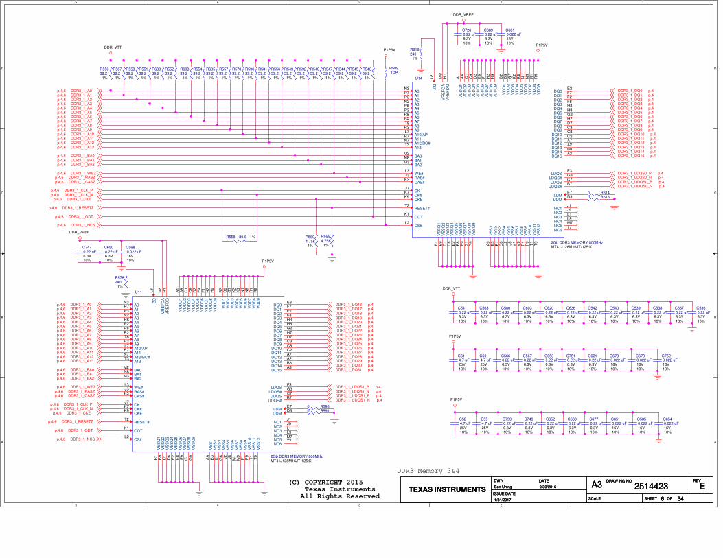
DDR3 Memory 3&4
DDR_VREF
P1P5VDDR_VTT
DDR_VTT
P1P5V
P1P5V
DDR_VREF
P1P5V
P1P5V
DDR3_1_CLK_Pp.4,6DDR3_1_CLK_Np.4,6
DDR3_1_DQ11 p.4DDR3_1_DQ12 p.4DDR3_1_DQ13 p.4
DDR3_1_DQ10 p.4
DDR3_1_RESETZp.4,6
DDR3_1_ODTp.4,6
DDR3_1_A1p.4,6
DDR3_1_DQ14 p.4DDR3_1_DQ15 p.4
DDR3_1_A2p.4,6DDR3_1_A3p.4,6DDR3_1_A4p.4,6DDR3_1_A5p.4,6
DDR3_1_LDQS0_P p.4DDR3_1_LDQS0_N p.4DDR3_1_UDQS0_P p.4DDR3_1_UDQS0_N p.4
DDR3_1_DQ1 p.4DDR3_1_DQ2 p.4DDR3_1_DQ3 p.4DDR3_1_DQ4 p.4DDR3_1_DQ5 p.4
DDR3_1_DQ7 p.4DDR3_1_DQ8 p.4DDR3_1_DQ9 p.4
DDR3_1_DQ6 p.4
DDR3_1_DQ0 p.4
DDR3_1_A7p.4,6DDR3_1_A8p.4,6DDR3_1_A9p.4,6DDR3_1_A10p.4,6DDR3_1_A11p.4,6
DDR3_1_A6p.4,6
DDR3_1_A12p.4,6DDR3_1_A13p.4,6
DDR3_1_BA0p.4,6DDR3_1_BA1p.4,6DDR3_1_BA2p.4,6
DDR3_1_WEZp.4,6DDR3_1_RASZp.4,6
DDR3_1_A0p.4,6
DDR3_1_CASZp.4,6
DDR3_1_DQ27 p.4DDR3_1_DQ26 p.4
DDR3_1_DQ29 p.4DDR3_1_DQ28 p.4
DDR3_1_DQ31 p.4DDR3_1_DQ30 p.4
DDR3_1_LDQS1_P p.4
DDR3_1_UDQS1_N p.4DDR3_1_UDQS1_P p.4DDR3_1_LDQS1_N p.4
DDR3_1_DQ18 p.4DDR3_1_DQ17 p.4
DDR3_1_DQ21 p.4DDR3_1_DQ20 p.4DDR3_1_DQ19 p.4
DDR3_1_DQ25 p.4DDR3_1_DQ24 p.4DDR3_1_DQ23 p.4
DDR3_1_DQ16 p.4
DDR3_1_DQ22 p.4
DDR3_1_CLK_Pp.4,6DDR3_1_CLK_Np.4,6
DDR3_1_RESETZp.4,6
DDR3_1_ODTp.4,6
DDR3_1_A1p.4,6DDR3_1_A2p.4,6DDR3_1_A3p.4,6DDR3_1_A4p.4,6DDR3_1_A5p.4,6
DDR3_1_A7p.4,6DDR3_1_A8p.4,6DDR3_1_A9p.4,6DDR3_1_A10p.4,6DDR3_1_A11p.4,6
DDR3_1_A6p.4,6
DDR3_1_A12p.4,6DDR3_1_A13p.4,6
DDR3_1_BA0p.4,6DDR3_1_BA1p.4,6DDR3_1_BA2p.4,6
DDR3_1_WEZp.4,6DDR3_1_RASZp.4,6
DDR3_1_A0p.4,6
DDR3_1_CASZp.4,6
DDR3_1_CKEp.4,6
DDR3_1_CKEp.4,6
DDR3_1_NCSp.4,6
DDR3_1_NCSp.4,6
TEXAS INSTRUMENTS
DWN DATE
ISSUE DATE
SCALE
DRAWING NO REV
SHEET OF
2514423 EA3
346
Ben Uhing 9/30/2016
1/31/2017
TEXAS INSTRUMENTS
DWN DATE
ISSUE DATE
SCALE
DRAWING NO REV
SHEET OF
2514423 EA3
346
Ben Uhing 9/30/2016
1/31/2017
TEXAS INSTRUMENTS
DWN DATE
ISSUE DATE
SCALE
DRAWING NO REV
SHEET OF
2514423 EA3
346
Ben Uhing 9/30/2016
1/31/2017
C5850.022 uF16V10%
R55739.2
1%
R54639.2
1%
C7510.22 uF6.3V10%
C604.7 uF25V10%
C5800.22 uF6.3V10%
C524.7 uF25V10%
R578240
1%
R558 80.6 1%
R57339.2
1%
C7470.22 uF6.3V10%
C6210.22 uF6.3V10%
C6030.22 uF6.3V10%
C6540.022 uF16V10%
R5554.75K
1%
R59639.2
1%
C554.7 uF25V10%
R616240
1%
C6780.022 uF16V10%
C6200.22 uF6.3V10%
C6500.22 uF6.3V10%
R5604.75K
1%
R58739.2
1%
R58139.2
1%
C6790.022 uF16V10%
C6360.22 uF6.3V10%
C7260.22 uF6.3V10%
R55339.2
1%
R55639.2
1%
U11
2Gb DDR3 MEMORY 800MHzMT41J128M16JT-125:K
A0N3
A1P7
A2P3
A3N2
A4P8
A5P2
A6R8
A7R2
A8T8
A9R3
A10/APL7
A11R7
A12/BC#N7
A13T3
BA0M2
BA1N8
BA2M3
WE#L3
RAS#J3
CAS#K3
CKJ7
CK#K7
CKEK9
RESET#T2
ODTK1
CS#L2
VS
SQ
1B
1
VS
SQ
2B
9
VS
SQ
3D
1
VS
SQ
4D
8
VS
SQ
5E
2
VS
SQ
6E
8
VS
SQ
7F
9
VS
SQ
8G
1
VS
SQ
9G
9
VS
S1
A9
VS
S2
B3
VS
S3
E1
VS
S4
G8
VS
S5
J2
VS
S6
J8
VS
S7
M1
VS
S8
M9
VS
S9
P1
VS
S10
P9
VS
S11
T1
VS
S12
T9
DQ0E3
DQ1F7
DQ2F2
DQ3F8
DQ4H3
DQ5H8
DQ6G2
DQ7H7
DQ8D7
DQ9C3
DQ10C8
DQ11C2
DQ12A7
DQ13A2
DQ14B8
DQ15A3
LDQSF3
LDQS#G3
UDQSC7
UDQS#B7
LDME7
UDMD3
ZQ
L8
VR
EF
CA
M8
VR
EF
DQ
H1
VD
DQ
1A
1
VD
DQ
2A
8
VD
DQ
3C
1
VD
DQ
4C
9
VD
DQ
5D
2
VD
DQ
6E
9
VD
DQ
7F
1
VD
DQ
8H
2
VD
DQ
9H
9
VD
D1
B2
VD
D2
D9
VD
D3
G7
VD
D4
K2
VD
D5
K8
VD
D6
N1
VD
D7
N9
VD
D8
R1
VD
D9
R9
NC1J1
NC2J9
NC3L1
NC4L9
NC5M7
NC6T7
C7520.022 uF16V10%
C5420.22 uF6.3V10%
R54939.2
1%
C6890.22 uF6.3V10%
C5680.022 uF16V10%
R55139.2
1% U14
2Gb DDR3 MEMORY 800MHzMT41J128M16JT-125:K
A0N3
A1P7
A2P3
A3N2
A4P8
A5P2
A6R8
A7R2
A8T8
A9R3
A10/APL7
A11R7
A12/BC#N7
A13T3
BA0M2
BA1N8
BA2M3
WE#L3
RAS#J3
CAS#K3
CKJ7
CK#K7
CKEK9
RESET#T2
ODTK1
CS#L2
VS
SQ
1B
1
VS
SQ
2B
9
VS
SQ
3D
1
VS
SQ
4D
8
VS
SQ
5E
2
VS
SQ
6E
8
VS
SQ
7F
9
VS
SQ
8G
1
VS
SQ
9G
9
VS
S1
A9
VS
S2
B3
VS
S3
E1
VS
S4
G8
VS
S5
J2
VS
S6
J8
VS
S7
M1
VS
S8
M9
VS
S9
P1
VS
S10
P9
VS
S11
T1
VS
S12
T9
DQ0E3
DQ1F7
DQ2F2
DQ3F8
DQ4H3
DQ5H8
DQ6G2
DQ7H7
DQ8D7
DQ9C3
DQ10C8
DQ11C2
DQ12A7
DQ13A2
DQ14B8
DQ15A3
LDQSF3
LDQS#G3
UDQSC7
UDQS#B7
LDME7
UDMD3
ZQ
L8
VR
EF
CA
M8
VR
EF
DQ
H1
VD
DQ
1A
1
VD
DQ
2A
8
VD
DQ
3C
1
VD
DQ
4C
9
VD
DQ
5D
2
VD
DQ
6E
9
VD
DQ
7F
1
VD
DQ
8H
2
VD
DQ
9H
9
VD
D1
B2
VD
D2
D9
VD
D3
G7
VD
D4
K2
VD
D5
K8
VD
D6
N1
VD
D7
N9
VD
D8
R1
VD
D9
R9
NC1J1
NC2J9
NC3L1
NC4L9
NC5M7
NC6T7
C7490.22 uF6.3V10%
R60039.2
1%
R59239.2
1%
C5400.22 uF6.3V10%
C6520.22 uF6.3V10%
C6810.022 uF16V10%
R55239.2
1%
R54839.2
1%
C5390.22 uF6.3V10%
C7500.22 uF6.3V10%
R55039.2
1%
C6800.22 uF6.3V10%
R60339.2
1%
R54739.2
1%
C5380.22 uF6.3V10%
C614.7 uF25V10%
R5950
C6770.22 uF6.3V10%
C5660.22 uF6.3V10%
C5410.22 uF6.3V10%
R6140
R55439.2
1%
R54439.2
1%
C5370.22 uF6.3V10%
R58910K
C5670.22 uF6.3V10%
R5910
C6510.022 uF16V10%
R6130
R60539.2
1%
R54539.2
1%
C6530.22 uF6.3V10%
C5360.22 uF6.3V10%
C5630.22 uF6.3V10%
5
5
4
4
3
3
2
2
1
1
D D
C C
B B
A A
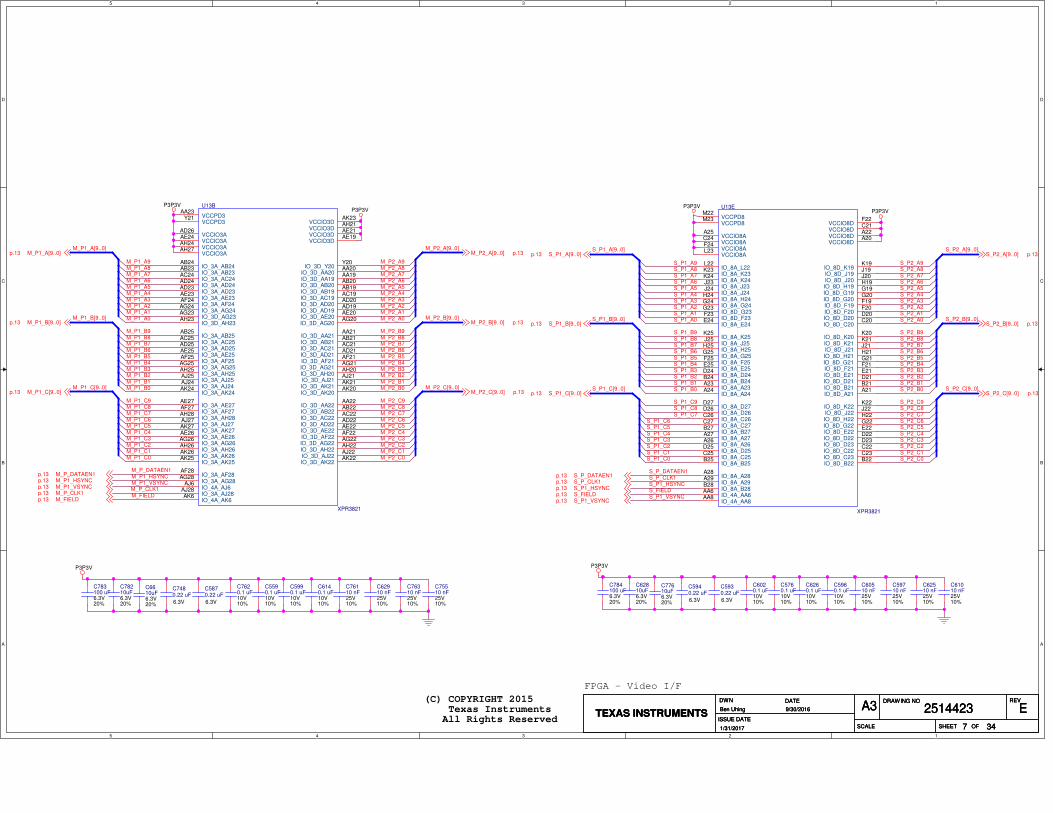
FPGA - Video I/F
(C) COPYRIGHT 2015 Texas Instruments All Rights Reserved
P3P3VP3P3VP3P3V P3P3V
P3P3V P3P3V
M_P1_A[9..0]p.13
M_P1_B[9..0]p.13
M_P1_C[9..0]p.13
S_P1_A[9..0]p.13
S_P1_B[9..0]p.13
S_P1_C[9..0]p.13
M_P2_A[9..0] p.13
M_P2_B[9..0] p.13
M_P2_C[9..0] p.13
S_P2_A[9..0] p.13
S_P2_B[9..0] p.13
S_P2_C[9..0] p.13
M_P_DATAEN1p.13M_P1_HSYNCp.13M_P1_VSYNCp.13M_P_CLK1p.13M_FIELDp.13
S_P_DATAEN1p.13
S_P1_HSYNCp.13
S_P1_VSYNCp.13
S_P_CLK1p.13
S_FIELDp.13
TEXAS INSTRUMENTS
DWN DATE
ISSUE DATE
SCALE
DRAWING NO REV
SHEET OF
2514423 EA3
347
Ben Uhing 9/30/2016
1/31/2017
TEXAS INSTRUMENTS
DWN DATE
ISSUE DATE
SCALE
DRAWING NO REV
SHEET OF
2514423 EA3
347
Ben Uhing 9/30/2016
1/31/2017
TEXAS INSTRUMENTS
DWN DATE
ISSUE DATE
SCALE
DRAWING NO REV
SHEET OF
2514423 EA3
347
Ben Uhing 9/30/2016
1/31/2017
C7620.1 uF10V10%
C62910 nF25V10%
U13B
XPR3821
IO_3A_AJ27AJ27
IO_3A_AK27AK27
IO_3A_AB25AB25
IO_3A_AC25AC25
IO_3D_AA19AA19
IO_3D_AB19AB19
IO_3D_AG20AG20
IO_3D_AH20AH20
IO_3A_AG28AG28
IO_3A_AE27AE27
IO_3A_AE26AE26
IO_3A_AE25AE25
IO_3A_AK26AK26
IO_3A_AK25AK25
IO_3A_AB23AB23 IO_3A_AB24AB24
IO_3A_AH25AH25
IO_3A_AJ25AJ25
IO_3A_AC24AC24
IO_3A_AD24AD24
IO_3A_AF24AF24
IO_3A_AG24AG24
IO_3A_AD23AD23
IO_3A_AE23AE23
IO_3A_AJ24AJ24
IO_3A_AK24AK24
IO_3D_AC22AC22
IO_3D_AD22AD22
IO_3D_AA22AA22
IO_3D_AB22AB22
IO_3D_AB21AB21
IO_3D_AC21AC21
IO_3D_AG23AG23
IO_3D_AH23AH23
IO_3D_AD21AD21
IO_3D_AE22AE22
IO_3D_AF22AF22
IO_3D_AG22AG22
IO_3D_Y20Y20
IO_3D_AD20AD20
IO_3D_AE20AE20
IO_3D_AA20AA20
IO_3D_AB20AB20
IO_3D_AC19AC19
IO_3D_AD19AD19
VCCPD3AA23
VCCPD3Y21
VCCIO3AAD26
VCCIO3AAE24
VCCIO3AAH24
VCCIO3AAH27
VCCIO3DAE19VCCIO3DAE21VCCIO3DAH21VCCIO3DAK23
IO_3A_AD25AD25
IO_3A_AF25AF25
IO_3A_AG25AG25
IO_3A_AF27AF27
IO_3A_AG26AG26
IO_3A_AH26AH26
IO_3A_AF28AF28
IO_3A_AJ28AJ28
IO_4A_AK6AK6
IO_3D_AA21AA21
IO_3D_AF21AF21
IO_3D_AG21AG21
IO_3D_AH22AH22
IO_3D_AJ22AJ22
IO_3D_AJ21AJ21
IO_3D_AK22AK22
IO_3D_AK20AK20IO_3D_AK21AK21
IO_4A_AJ6AJ6
IO_3A_AH28AH28
C783100 uF6.3V20%
C59710 nF25V10%
C5590.1 uF10V10%
C75510 nF25V10%
C6020.1 uF10V10%
C78210uF6.3V20%
C61010 nF25V10%
C784100 uF6.3V20%
C76310 nF25V10%
C62510 nF25V10%
C5760.1 uF10V10%
C5990.1 uF10V10%
C62810uF6.3V20%
U13E
XPR3821
IO_8A_C27C27 IO_8A_C26C26
IO_8A_A28A28
IO_8A_B27B27
IO_8D_C20C20IO_8D_D20D20
IO_8D_G19G19IO_8D_H19H19
IO_8A_A23A23
IO_8A_A24A24
IO_8A_L22L22
IO_8A_K23K23
IO_8A_D24D24
IO_8A_E24E24
IO_8A_B24B24
IO_8A_B25B25
IO_8A_A26A26 IO_8A_A27A27
IO_8A_K24K24
IO_8A_J23J23
IO_8A_J25J25 IO_8A_K25K25
IO_8A_G24G24 IO_8A_H24H24 IO_8A_J24J24
IO_8A_F25F25
IO_8D_J19J19IO_8D_K19K19
IO_8D_F20F20
IO_8D_F21F21
IO_8D_D21D21IO_8D_E21E21
IO_8D_J21J21
IO_8D_J22J22IO_8D_K22K22
IO_8D_G22G22IO_8D_H22H22
IO_8D_B22B22
IO_8D_C22C22
IO_8D_G21G21IO_8D_H21H21
IO_8D_F23F23 IO_8D_G23G23
IO_8D_C23C23
IO_8D_D23D23
VCCIO8AA25
VCCIO8AC24
VCCIO8AF24
VCCIO8AL23
VCCIO8DA20VCCIO8DA22VCCIO8DC21VCCIO8DF22VCCPD8
M22
VCCPD8M23
IO_8A_G25G25 IO_8A_H25H25
IO_8A_E25E25
IO_8A_D26D26 IO_8A_D27D27
IO_8A_D25D25
IO_8A_C25C25
IO_8A_A29A29
IO_8A_B28B28
IO_8D_J20J20
IO_8D_K20K20
IO_8D_A21A21IO_8D_B21B21
IO_8D_D22D22IO_8D_E22E22
IO_8D_F19F19IO_8D_G20G20
IO_8D_K21K21
IO_4A_AA6AA6
IO_4A_AA8AA8
C6610uF6.3V20%
C5870.22 uF
6.3V
C6140.1 uF10V10%
C6260.1 uF10V10%
C77610uF6.3V20%
C60510 nF25V10%
C7480.22 uF
6.3V
C5960.1 uF10V10%
C5930.22 uF
6.3V
C76110 nF25V10%
C5940.22 uF
6.3V
M_P1_A9M_P1_A8M_P1_A7M_P1_A6M_P1_A5M_P1_A4M_P1_A3M_P1_A2M_P1_A1M_P1_A0
M_P1_B9M_P1_B8M_P1_B7M_P1_B6M_P1_B5M_P1_B4M_P1_B3M_P1_B2M_P1_B1M_P1_B0
M_P1_C9M_P1_C8M_P1_C7M_P1_C6M_P1_C5M_P1_C4M_P1_C3M_P1_C2M_P1_C1M_P1_C0
M_P2_A9M_P2_A8M_P2_A7M_P2_A6M_P2_A5M_P2_A4M_P2_A3M_P2_A2M_P2_A1M_P2_A0
M_P2_B9M_P2_B8M_P2_B7M_P2_B6M_P2_B5M_P2_B4M_P2_B3M_P2_B2M_P2_B1M_P2_B0
M_P2_C9M_P2_C8M_P2_C7M_P2_C6M_P2_C5M_P2_C4M_P2_C3M_P2_C2M_P2_C1M_P2_C0
M_P1_A[9..0]
M_P1_B[9..0]
M_P1_C[9..0]
M_P2_A[9..0]
M_P2_B[9..0]
M_P2_C[9..0]
S_P1_A9S_P1_A8S_P1_A7S_P1_A6S_P1_A5S_P1_A4S_P1_A3S_P1_A2S_P1_A1S_P1_A0
S_P1_B9S_P1_B8S_P1_B7S_P1_B6S_P1_B5S_P1_B4S_P1_B3S_P1_B2S_P1_B1S_P1_B0
S_P1_C9S_P1_C8S_P1_C7
S_P1_C6S_P1_C5S_P1_C4S_P1_C3S_P1_C2S_P1_C1S_P1_C0
S_P1_A[9..0]
S_P1_B[9..0]
S_P1_C[9..0]
S_P2_A9S_P2_A8S_P2_A7S_P2_A6S_P2_A5S_P2_A4S_P2_A3S_P2_A2S_P2_A1S_P2_A0
S_P2_B9S_P2_B8S_P2_B7S_P2_B6S_P2_B5S_P2_B4S_P2_B3S_P2_B2S_P2_B1S_P2_B0
S_P2_C9S_P2_C8S_P2_C7S_P2_C6S_P2_C5S_P2_C4S_P2_C3S_P2_C2S_P2_C1S_P2_C0
S_P2_A[9..0]
S_P2_B[9..0]
S_P2_C[9..0]
M_P_CLK1M_FIELD
M_P1_VSYNCM_P1_HSYNCM_P_DATAEN1
S_FIELDS_P1_VSYNC
S_P1_HSYNCS_P_CLK1S_P_DATAEN1
5
5
4
4
3
3
2
2
1
1
D D
C C
B B
A A
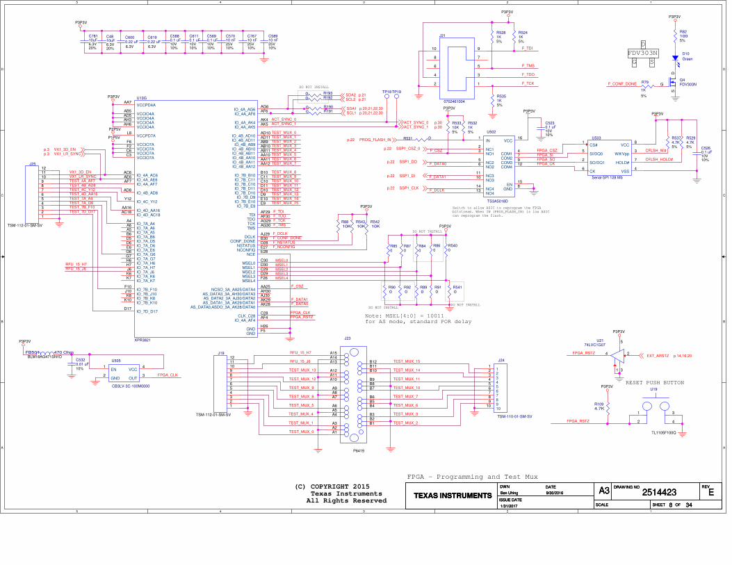
FPGA - Programming and Test Mux
DO NOT INSTALL
DO NOT INSTALLDO NOT INSTALL
G
D
FDV303N
S
RESET PUSH BUTTON
Note: MSEL[4:0] = 10011 for AS mode, standard POR delay
(C) COPYRIGHT 2015 Texas Instruments All Rights Reserved
Switch to allow ASIC to reprogram the FPGAbitstream. When IN (PROG_FLASH_IN) is low ASICcan reprogram the flash.
DO NOT INSTALL
P3P3V
P3P3V
P3P3V
P3P3V
P3P3V
P3P3V
P3P3V
P3P3V
P3P3V
P3P3V
P3P3VP3P3V
P1P5V
P2P5V
ACT_SYNC_0 p.30ACT_SYNC_1 p.30
EXT_ARSTZ p.14,16,20
SSP1_CSZ_0p.22
SSP1_DOp.22
SSP1_CLKp.22
SSP1_DIp.22
PROG_FLASH_INp.22
VX1_3D_ENp.3VX1_LR_SYNCp.3
SDA2 p.21SCL2 p.21
SDA1 p.20,21,22,30SCL1 p.20,21,22,30
TEXAS INSTRUMENTS
DWN DATE
ISSUE DATE
SCALE
DRAWING NO REV
SHEET OF
2514423 EA3
348
Ben Uhing 9/30/2016
1/31/2017
TEXAS INSTRUMENTS
DWN DATE
ISSUE DATE
SCALE
DRAWING NO REV
SHEET OF
2514423 EA3
348
Ben Uhing 9/30/2016
1/31/2017
TEXAS INSTRUMENTS
DWN DATE
ISSUE DATE
SCALE
DRAWING NO REV
SHEET OF
2514423 EA3
348
Ben Uhing 9/30/2016
1/31/2017
C78110uF6.3V20%
R531 0
R53310K5% U502
TS3A5018D
IN1
NC12
NO13
COM14
NC25
NO26
COM27
GND8
COM39
NO310 NC311
COM412
NO413 NC414 EN
15
VCC16
R5400
J24
TSM-110-01-SM-SV
11
22
33
44
55
66
77
88
99
1010
R821005%
R5321K5%
U503
Serial-SPI 128 Mb
CS#1
SO/DQ12
W#/Vpp3
SI/DQ05
HOLD#7
CK6
VCC8
VSS4
R1930
U19
TL1105F100Q
1
2
3
4
J19
TSM-112-01-SM-SV
123456789101112
C5690.1 uF10V10%
C4810uF6.3V20%
R5351K5%
R900
R8810K
C57010 nF25V10%
R5374.7K5%
R54310K
R5281K5%
U2174LVC1G07
24
5
1 3
R920
C6190.22 uF
6.3V
J23
P6419
B1B2B3
B4B5B6
B7B8B9
B10B11B12
A15A14A13
A12A11A10
A9A8A7
A6A5A4
A3A2A1
R5294.7K5%
U13G
XPR3821
NCSO_3A_AA25/DATA4AA25
AS_DATA3_3A_AH30/DATA3AH30
AS_DATA2_3A_AJ30/DATA2AJ30
AS_DATA1_3A_AK29/DATA1AK29
AS_DATA0,ASDO_3A_AK28/DATA0AK28
IO_4A_AF7AF7
IO_4A_AG6AG6
IO_4A_AK5AK5IO_4A_AK4AK4
IO_7A_K7K7
IO_7A_D6D6
IO_7A_E6E6
IO_7A_G6G6
IO_7A_H6H6 IO_7A_G7G7
TDOAF30
TMSAG30TCKAG29
TDIAF29
DCLKAJ29
CONF_DONEB30
NSTATUSD28
NCEE28NCONFIGE27
MSEL0C30
MSEL1D30
MSEL2C29
MSEL3D29
MSEL4F26
IO_7A_J6J6
IO_7A_K6K6
IO_4A_AF6AF6
IO_4A_AE6AE6 IO_4A_AC6AC6
IO_7A_D5D5
VCCPD4AAA7
VCCPD7AL8
VCCIO4AAB5
VCCIO4AAD5
VCCIO4AAH3
VCCIO4AAH6
VCCIO7AC3 VCCIO7AC6 VCCIO7AF2 VCCIO7AF6
GNDH26
GNDF5
CLK_C28C28
IO_4A_AF4AF4
IO_4B_AA10AA10
IO_4B_AA11AA11
IO_4B_AA12AA12
IO_4B_AB9AB9
IO_4B_AB10AB10
IO_4B_AB11AB11
IO_4B_AD8AD8
IO_4B_AD10AD10
IO_4B_AD11AD11
IO_4C_Y12Y12 IO_7B_D9
D9IO_7B_D10D10
IO_7B_E9E9IO_7B_E10E10
IO_7B_F10F10
IO_7B_J10J10
IO_7B_K8K8
IO_7B_K10K10
IO_7B_B10B10
IO_7B_C10C10IO_7B_C11C11
IO_7B_D11D11
IO_7A_H7H7
IO_4D_AA16AA16
IO_4D_AC18AC18
IO_7A_A4A4
IO_7A_B6B6
IO_7D_D17D17
IO_7A_A6A6
IO_7A_A5A5
R5241K5%
FB501 470 OhmBLM18AG471SN1D
C6000.22 uF
6.3V
R890
TP18
R850
C5320.01 uF10%
R910
TP19
Q4FDV303NG
DS
C5260.1 uF10V10%
C76710 nF25V10%
R870
J21
0702461004
10 9
8 7
6 5
4 3
2 1
R1094.7K
R5410
R1900
C5230.1 uF10V10%
D10
Green
C5880.1 uF10V10%
R840
R54210K
R79
1K
5%
R1910
U505
CB3LV-3C-100M0000
EN1
GND2
OUT3
VCC4
J25
TSM-112-01-SM-SV
123456789101112
R860
C58910 nF25V10%
C6110.1 uF10V10%
R1920
VX1_3D_ENVX1_LR_SYNCTEST_4A_AF7TEST_4B_AD8TEST_4C_Y12TEST_4D_AA16TEST_7A_A4TEST_7A_G6TEST_7B_F10
TEST_MUX_0TEST_MUX_1TEST_MUX_2TEST_MUX_3TEST_MUX_4TEST_MUX_5TEST_MUX_6TEST_MUX_7
TEST_MUX_8TEST_MUX_9TEST_MUX_10TEST_MUX_11TEST_MUX_12TEST_MUX_13TEST_MUX_14TEST_MUX_15
TEST_MUX_0
TEST_MUX_1 TEST_MUX_2
TEST_MUX_3TEST_MUX_4
TEST_MUX_5 TEST_MUX_6
TEST_MUX_7TEST_MUX_8
TEST_MUX_9 TEST_MUX_10
TEST_MUX_11TEST_MUX_12
TEST_MUX_13 TEST_MUX_14
TEST_MUX_15
RFU_15_H7
RFU_15_J6
F_TDO
F_TMS
F_TDI
F_TCK
F_TDI
F_TCKF_TMS
F_TDO
MSEL0MSEL1MSEL2MSEL3MSEL4
F_CONF_DONEF_NSTATUSF_NCONFIG
F_DCLK
F_DATA0
F_CONF_DONE
ACT_SYNC_0ACT_SYNC_1
FPGA_CLKFPGA_RSTZ
FPGA_RSTZ
TEST_7D_D17
FPGA_CLK
CFLSH_W#
CFLSH_HOLD#
F_CSZ
F_DATA1
FPGA_RSTZ
F_DATA0
F_DATA1
F_DCLK
F_CSZ FPGA_CSZFPGA_SIFPGA_SOFPGA_CK
RFU_15_H7RFU_15_J6

5
5
4
4
3
3
2
2
1
1
D D
C C
B B
A A
FPGA - Power
(C) COPYRIGHT 2015 Texas Instruments All Rights Reserved
P1P1V_FIL
P1P5V_FIL
P2P5V_FIL
P3P3V
P2P5V
P1P1V
P2P5V
P1P1V
P1P1V_FIL
P1P5V_FIL
P3P3V
P2P5V
P2P5V_FIL
TEXAS INSTRUMENTS
DWN DATE
ISSUE DATE
SCALE
DRAWING NO REV
SHEET OF
2514423 EA3
349
Ben Uhing 9/30/2016
1/31/2017
TEXAS INSTRUMENTS
DWN DATE
ISSUE DATE
SCALE
DRAWING NO REV
SHEET OF
2514423 EA3
349
Ben Uhing 9/30/2016
1/31/2017
TEXAS INSTRUMENTS
DWN DATE
ISSUE DATE
SCALE
DRAWING NO REV
SHEET OF
2514423 EA3
349
Ben Uhing 9/30/2016
1/31/2017
C71810 nF25V10%
C73610 nF25V10%
C70610 nF25V10%
C6580.1 uF10V10%
C60810 nF25V10%
C68710 nF25V10%
C7150.1 uF10V10%
C6150.1 uF10V10%
C77510uF6.3V20%
C7040.22 uF
6.3V
C7070.1 uF10V10%
C6350.1 uF10V10%
C52710uF6.3V20%
C70010 nF25V10%
C5780.1 uF10V10%
C61610 nF25V10%
C6750.1 uF10V10%
C6390.22 uF
6.3V
C7080.1 uF10V10%
C60110 nF25V10%
C7350.1 uF10V10%
C6300.1 uF10V10%
C7010.22 uF
6.3V
C61710 nF25V10%
C6040.1 uF10V10%
C6640.22 uF
6.3V
C6240.22 uF
6.3V
C71410 nF25V10%
C7240.1 uF10V10%
C6340.1 uF10V10%
C6620.22 uF
6.3V
C64510 nF25V10%
C73810 nF25V10%
C5910.1 uF10V10%
C6460.1 uF10V10%
C6230.1 uF10V10%
C6400.22 uF
6.3V
C6330.1 uF10V10%
C771100 uF6.3V20%
C4610uF6.3V20%
C6660.1 uF10V10%
C23100 uF6.3V20%
C6630.1 uF10V10%
C7120.1 uF10V10%
C77210uF6.3V20%
C54410uF6.3V20%
C6410.22 uF
6.3V
C61210 nF25V10%
C6990.1 uF10V10%
C73410 nF25V10%
C5900.1 uF10V10%
C6820.1 uF10V10%
C6180.1 uF10V10%
C7400.1 uF10V10%
C7370.22 uF
6.3V
C4910uF6.3V20%
U13F
XPR3821
NC_AJ3AJ3
NC_AK3AK3
NC_AJ1AJ1
NC_AK2AK2
NC_AH2AH2 NC_AH1AH1
NC_E1E1
NC_D2D2 NC_D1D1
NC_A2A2
NC_B1B1
NC_F8F8
NC_G8G8
NC_J8J8
NC_E7E7
NC_F7F7
NC_G9G9
NC_H9H9
NC_A7A7
NC_A8A8
NC_B7B7
NC_C7C7
NC_C8C8
NC_D8D8
NC_J9J9
NC_B9B9
NC_AC10AC10
NC_AE9AE9
NC_AF9AF9
NC_AJ9AJ9
NC_AK8AK8
NC_AC9AC9
NC_AD9AD9
NC_AB8AB8
NC_AG8AG8
NC_AH8AH8
NC_AJ7AJ7
NC_AK7AK7
NC_AE8AE8
NC_AG7AG7
NC_AH7AH7
NC_A3A3
NC_B3B3
NC_B4B4
NC_C4C4
DNU_E3E3
NC_D4D4 NC_D3D3
NC_C2C2 NC_C1C1
NC_J7J7
NC_AG5AG5
NC_AH5AH5 NC_AH4AH4
NC_AJ4AJ4
NC_AC7AC7
NC_AD6AD6
DNU_AE5AE5
NC_AG4AG4 NC_AG3AG3
DNU_AB26AB26
DNU_AF2AF2
DNU_AG2AG2
DNU_E29E29
DNU_F29F29
DNU_H5H5
DNU_17K15
DNU_Y16Y16
DNU_L3L3
DNU_L4L4
DNU_AC4AC4DNU_AC3AC3
DNU_J4J4DNU_J3J3
DNU_G4G4DNU_G3G3
DNU_AA4AA4DNU_AA3AA3
DNU_W4W4DNU_W3W3
DNU_U4U4DNU_U3U3
DNU_R4R4DNU_R3R3DNU_N4N4DNU_N3N3
DNU_AA1AA1
DNU_AC1AC1
DNU_J1J1
DNU_K4K4
DNU_L1L1
DNU_M4M4
DNU_N1N1
DNU_R7R7
DNU_T8T8
DNU_U1U1
DNU_U7U7
DNU_V8V8
C63110 nF25V10%
C69210 nF25V10%
C6670.22 uF
6.3V
C6850.1 uF10V10%
C7110uF6.3V20%
C66110 nF25V10%
R1062K0.1%
C5920.1 uF10V10%
C6760.1 uF10V10%
U13A
XPR3821
VCCPL11
VCCPL15
VCCPL19
VCCPL20
VCCPL9
VCCPW11
VCCPW13
VCCPW17
VCCPW19
VCCPW21
VCCA_FPLLW16
VCCA_FPLLM16
VCCA_FPLLT22 VCCA_FPLLT9 VCCA_FPLL
P22 VCCA_FPLLP9
VCCBATK26
VCC_AUXM12
VCC_AUXM18
VCC_AUXW12
VCC_AUXW18
VCCD_FPLLW15
VCCD_FPLLM15
VCCD_FPLLV22 VCCD_FPLLV9 VCCD_FPLL
N22
VCCD_FPLLM8
VCCPGMK5 VCCPGM
AA24
VCCM10
VCCM14
VCCM20
VCCN11
VCCN13
VCCN15
VCCN17
VCCN19
VCCN21
VCCP10
VCCP12
VCCP14
VCCP16
VCCP18
VCCP20
VCCR11
VCCR13
VCCR15
VCCR17
VCCR19
VCCR21
VCCT10
VCCT12
VCCT14
VCCT18
VCCT20
VCCU11
VCCU13
VCCU15
VCCU17
VCCU19
VCCU21
VCCV10
VCCV12
VCCV14
VCCV16
VCCV18
VCCV20
VCCT16
VCCIO5AAE4
VCCPD5AA9
VCCIO6AF1
VCCPD6K9
RREF_TLF30
RREF_BRAF1
C6480.22 uF
6.3V
C6320.1 uF10V10%
C6380.1 uF10V10%
C4510uF6.3V20%
C7090.1 uF10V10%
C68610 nF25V10%
C72310 nF25V10%
C72510 nF25V10%
C7130.1 uF10V10%
C71710 nF25V10%
C6420.1 uF10V10%
C53010uF6.3V20%
C6830.22 uF
6.3V
C7190.1 uF10V10%
C6070.22 uF
6.3VR932K0.1%
C7640.1 uF10V10%
C4710uF6.3V20%
C6220.1 uF10V10%
C6900.1 uF10V10%
C6570.1 uF10V10%
5
5
4
4
3
3
2
2
1
1
D D
C C
B B
A A
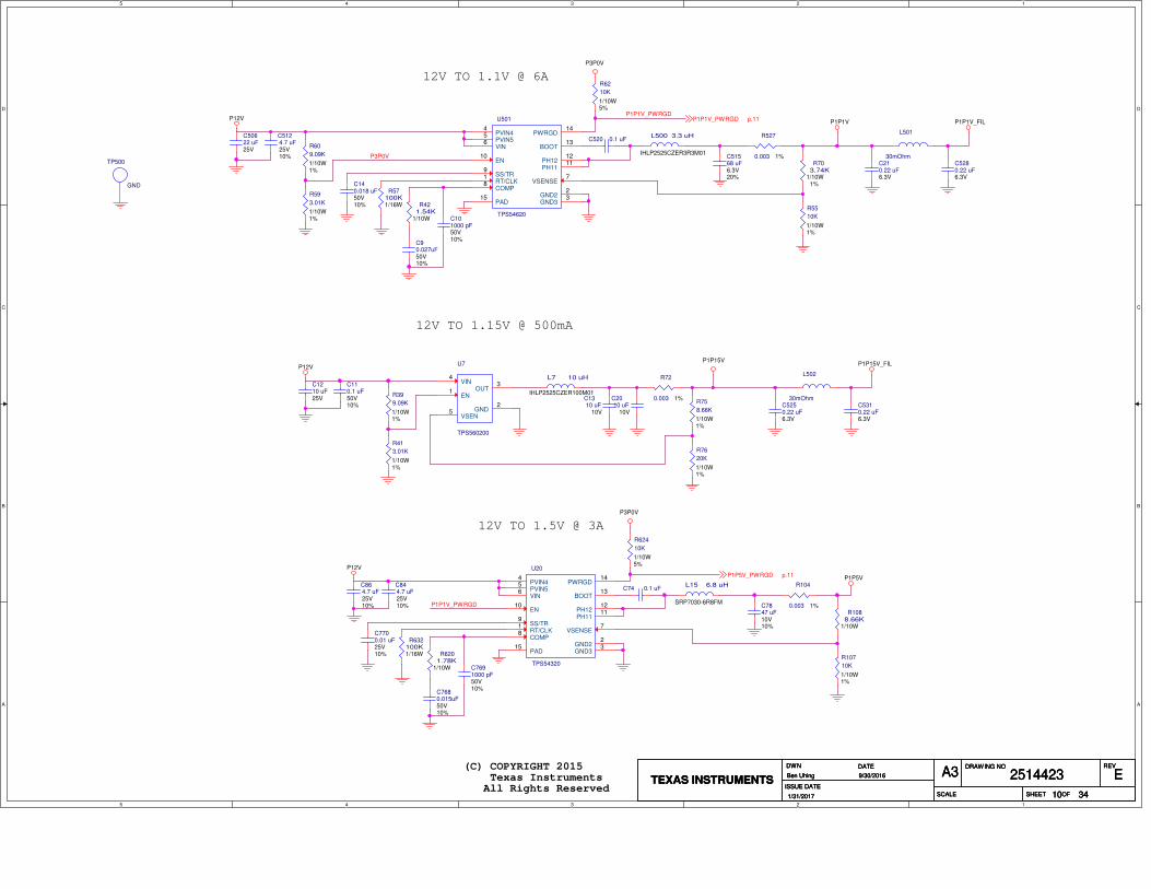
12V TO 1.15V @ 500mA
12V TO 1.1V @ 6A
12V TO 1.5V @ 3A
(C) COPYRIGHT 2015 Texas Instruments All Rights Reserved
P1P1V_FIL
P1P15VP1P15V_FIL
P12V
P3P0V
P1P1V
P12V
P12V
P3P0V
P1P5VP1P5V_PWRGD p.11
P1P1V_PWRGD p.11
TEXAS INSTRUMENTS
DWN DATE
ISSUE DATE
SCALE
DRAWING NO REV
SHEET OF
2514423 EA3
3410
Ben Uhing 9/30/2016
1/31/2017
TEXAS INSTRUMENTS
DWN DATE
ISSUE DATE
SCALE
DRAWING NO REV
SHEET OF
2514423 EA3
3410
Ben Uhing 9/30/2016
1/31/2017
TEXAS INSTRUMENTS
DWN DATE
ISSUE DATE
SCALE
DRAWING NO REV
SHEET OF
2514423 EA3
3410
Ben Uhing 9/30/2016
1/31/2017
R75
8.66K
1%1/10W
L15 6.8 uH
SRP7030-6R8FM
C90.027uF50V10%
C101000 pF50V10%
R60
9.09K
1%1/10WTP500
GND
C110.1 uF50V10%
R72
0.003 1%C5250.22 uF6.3V
U7
TPS560200
EN1
VIN4
OUT3
GND2
VSEN5
C140.018 uF50V10%
R41
3.01K
1%1/10W
R104
0.003 1%
C864.7 uF25V10%
C210.22 uF6.3V
C50622 uF25V
C5124.7 uF25V10% C515
68 uF6.3V20%
C7700.01 uF25V10%
R624
10K
5%1/10W
R59
3.01K
1%1/10W
R632100K1/16W
R57100K1/16W
C74 0.1 uFC844.7 uF25V10%
C1310 uF
10V
R421.54K
1/10W
R6201.78K
1/10W
C5280.22 uF6.3V
C2010 uF
10V
L7 10 uH
IHLP2525CZER100M01
C7691000 pF50V10%
R76
20K
1%1/10W
C520 0.1 uFL501
30mOhm
R527
0.003 1%
R107
10K
1%1/10W
C5310.22 uF6.3V
R62
10K
5%1/10W
R1088.66K
1/10W
U501
TPS54620
PVIN44
PVIN55
VIN6
EN10
PWRGD14
SS/TR9
RT/CLK1
COMP8
BOOT13
PH1212
PH1111
VSENSE7
GND22
GND33
PAD15
R55
10K
1%1/10W
C7847 uF10V10%
R39
9.09K
1%1/10W
C7680.015uF50V10%
L502
30mOhm
U20
TPS54320
PVIN44
PVIN55
VIN6
EN10
PWRGD14
SS/TR9
RT/CLK1
COMP8
BOOT13
PH1212
PH1111
VSENSE7
GND22
GND33
PAD15
L500 3.3 uH
IHLP2525CZER3R3M01
C1210 uF25V
R703.74K
1/10W1%
P3P0V
P1P1V_PWRGD
P1P1V_PWRGD

5
5
4
4
3
3
2
2
1
1
D D
C C
B B
A A
3.3V TO 2.5V @ 1.5A
12V TO 3.3V @ 3A
2.5V TO 1.5V @ 500mA
(DDR3 VDD)
(FPGA VCCAUX) (FPGA VCCD FPLL)
1.5V TO 0.75V DDR_VTT & DDR_VREF
DDR TERMINATION VOLTAGE
P1P1V
P1P5V
P3P3V P1P5VP2P5V
P1P15V
+0.75
(FPGA CORE)
(FPGA VCCIO)
(FPGA VCCPD)(FPGA VCCIO) (FPGA VCCH)
(FPGA VCCL,R,T)
(DDR_VTT)
(DDR_VREF)
+12V
Power Sequence
(C) COPYRIGHT 2015 Texas Instruments All Rights Reserved
Do Not Install
The connection from U24-15 to P3P3Vis a blue wire on existing Rev A pwb's.
P3P3V
P3P3V
P2P5V
P12V
P3P0V
P3P3V
P2P5V
P3P3V
P1P5V_FIL
P2P5V_FIL
P1P5V
P1P5V
DDR_VTT
DDR_VREF
P3P3VP3P3V
P5V_S P3P3V_PWRGDp.11
P2P5V_PWRGD p.11
P3P3V_PWRGD p.11
P2P5V_PWRGDp.11
P1P5V_PWRGD p.10
P1P1V_PWRGDp.10
TEXAS INSTRUMENTS
DWN DATE
ISSUE DATE
SCALE
DRAWING NO REV
SHEET OF
2514423 EA3
3411
Ben Uhing 9/30/2016
1/31/2017
TEXAS INSTRUMENTS
DWN DATE
ISSUE DATE
SCALE
DRAWING NO REV
SHEET OF
2514423 EA3
3411
Ben Uhing 9/30/2016
1/31/2017
TEXAS INSTRUMENTS
DWN DATE
ISSUE DATE
SCALE
DRAWING NO REV
SHEET OF
2514423 EA3
3411
Ben Uhing 9/30/2016
1/31/2017
C154.7 uF25V10%
R51831.6K
1/10W
L503
30mOhm
R622
10K
1%1/10W
R116
1.69K
1%1/10W
R525
10K
5%1/10W
C7910 uF10V10%
R115
0.003 1%
R623
10K
1%1/10W
R635
10K
5%1/10W
R526100K1/16W
C7730.001 uF10V10%
C17 0.1 uF
U23
TPS74701
IN_11
IN_22
OUT_210
PG3
OUT_19
EN5
BIAS4 FB
8
PAD11
GND6
SS7
C7770.22 uF6.3V
C164.7 uF25V10% C19
47 uF10V10%
C7310 uF10V10%
R519
10K
1%1/10W
L8 6.8 uH
SRP7030-6R8FM
C7210 uF10V10%
U24
TPS74301
IN_37
IN_15
IN_26
EN11
PWRGD9
BIAS10
OUT_11
IN_48
OUT_319OUT_218
OUT_420
FB16
GND12
PAD21SS
15
NC413NC514NC617
NC12
NC23
NC34
R113
0.003 1%
C7801 uF16V
R114
3.57K
1%1/10W
R636
4.75K
1%1/10W
R110
R
C7860.01 uF10%
C834.7 uF25V10%
C854.7 uF25V10%
C8010 uF10V10%
C821 uF16V
C5140.015uF50V10%
U18
TPS51200
VLDOIN2
VO3
PGND4
VOSNS5
REFOUT6
EN7
GND8
PAD11
PGOOD9
VIN10
REFIN1
R111
R
R634
4.12K
1%1/10W
C7710 uF10V10%
C5210.01 uF25V10%
C5191000 pF50V10%
C874.7 uF25V10%
R73
0.003 1%
C7850.01 uF10%
C7510 uF10V10%
C7780.22 uF6.3V
C810.1 uF10V
U9
TPS54320
PVIN44
PVIN55
VIN6
EN10
PWRGD14
SS/TR9
RT/CLK1
COMP8
BOOT13
PH1212
PH1111
VSENSE7
GND22
GND33
PAD15
R5201.78K
1/10W
C7610 uF10V10%
5
5
4
4
3
3
2
2
1
1
D D
C C
B B
A A
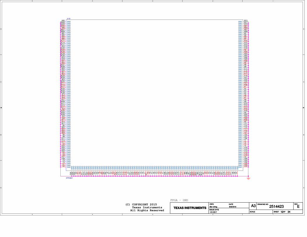
FPGA - GND
(C) COPYRIGHT 2015 Texas Instruments All Rights Reserved
TEXAS INSTRUMENTS
DWN DATE
ISSUE DATE
SCALE
DRAWING NO REV
SHEET OF
2514423 EA3
3412
Ben Uhing 9/30/2016
1/31/2017
TEXAS INSTRUMENTS
DWN DATE
ISSUE DATE
SCALE
DRAWING NO REV
SHEET OF
2514423 EA3
3412
Ben Uhing 9/30/2016
1/31/2017
TEXAS INSTRUMENTS
DWN DATE
ISSUE DATE
SCALE
DRAWING NO REV
SHEET OF
2514423 EA3
3412
Ben Uhing 9/30/2016
1/31/2017
U13I
XPR3821
GNDAA2
GNDAA26
GNDAA29
GNDAA30
GNDAA5
GNDAB27
GNDAB28
GNDAB3
GNDAB4
GNDAC11
GNDAC14
GNDAC17
GNDAC2
GNDAC20
GNDAC23
GNDAC26
GNDAC29
GNDAC30
GNDAC5
GNDAC8
GNDAD27
GNDAD28
GNDAD3
GNDAD4
GNDAE1
GNDAE2
GNDAE28
GNDAE29
GNDAE3
GNDAE30
GNDAF11
GNDAF14
GNDAF17
GNDAF20
GNDAF23
GNDAF26
GNDAF3
GNDAF5
GNDAF8
GNDAG1
GNDAH29
GNDAJ11
GNDAJ14
GNDAJ17
GNDAJ2
GNDAJ20
GNDAJ23
GNDAJ26
GNDAJ5
GNDAJ8
GNDB11
GNDB14
GNDB17
GNDB2
GNDB20
GNDB23
GNDB26
GNDB29
GNDB5
GNDB8
GNDE11
GNDE14
GNDE17
GNDE2
GNDE20
GNDE23
GNDE26
GNDE30
GNDE5
GNDE8
GNDF27
GNDF28
GNDF3
GNDF4
GNDG1
GNDG2
GN
DG
26
GN
DG
29
GN
DG
30
GN
DG
5
GN
DH
11
GN
DH
14
GN
DH
17
GN
DH
20
GN
DH
23
GN
DH
27
GN
DH
28
GN
DH
3
GN
DH
4
GN
DH
8
GN
DJ2
GN
DJ26
GN
DJ29
GN
DJ30
GN
DJ5
GN
DK
27
GN
DK
28
GN
DK
3
GN
DL10
GN
DL12
GN
DL14
GN
DL16
GN
DL18
GN
DL2
GN
DL21
GN
DL24
GN
DL25
GN
DL26
GN
DL29
GN
DL30
GN
DL5
GN
DL6
GN
DL7
GN
DM
11
GNDM13
GNDM17
GNDM19
GNDM21
GNDM24
GNDM27
GNDM28
GNDM3
GNDM7
GNDN10
GNDN12
GNDN14
GNDN16
GNDN18
GNDN2
GNDN20
GNDN23
GNDN24
GNDN26
GNDN29
GNDN30
GNDN5
GNDN8
GNDN9
GNDP11
GNDP13
GNDP15
GNDP17
GNDP19
GNDP21
GNDP23
GNDP25
GNDP27
GNDP28
GNDP3
GNDP4
GNDP6
GNDP8
GNDR1
GNDR10
GNDR12
GNDR14
GNDR16
GNDR18
GNDR2
GNDR20
GNDR24
GNDR29
GNDR30
GNDR5
GNDT11
GNDT13
GNDT15
GNDT17
GNDT19
GNDT21
GNDT23
GNDT27
GNDT28
GNDT3
GNDT4
GNDU10
GNDU12
GNDU14
GNDU16
GNDU18
GNDU2
GNDU20
GNDU24
GNDU26
GNDU29
GNDU30
GN
DU
5
GN
DV
11
GN
DV
13
GN
DV
15
GN
DV
17
GN
DV
19
GN
DV
21
GN
DV
23
GN
DV
25
GN
DV
27
GN
DV
28
GN
DV
3G
ND
V4
GN
DV
6G
ND
W1
GN
DW
10
GN
DW
14
GN
DW
2G
ND
W20
GN
DW
24
GN
DW
29
GN
DW
30
GN
DW
7
GN
DY
11
GN
DY
14
GN
DY
17
GN
DY
19
GN
DY
22
GN
DY
23
GN
DY
24
GN
DY
25
GN
DY
26
GN
DY
27
GN
DY
28
GN
DY
3G
ND
Y4
GN
DY
5G
ND
Y6
GN
DY
7G
ND
Y8
GN
DY
9
GNDR8
GNDR9
GN
DU
9
GN
DW
8G
ND
W9
GNDM1
GNDM2
GNDP1
GNDP2
GNDT1
GNDT2
GN
DV
1G
ND
V2
GN
DY
1G
ND
Y2
GNDAB1
GNDAB2
GN
DH
1
GN
DH
2
GN
DK
1
GN
DK
2
GNDAD1
GNDAD2
GN
DU
8

5
5
4
4
3
3
2
2
1
1
D D
C C
B B
A A
Master and Slave Front End Interface (C) COPYRIGHT 2015 Texas Instruments All Rights Reserved
SlaveMaster
M_P1_A[9..0]p.7
M_P1_B[9..0]p.7
M_P1_C[9..0]p.7
M_P2_A[9..0]p.7
M_P2_B[9..0]p.7
M_P2_C[9..0]p.7
M_P_CLK1p.7
M_P1_HSYNCp.7
M_P1_VSYNCp.7
M_P_DATAEN1p.7
M_FIELDp.7
S_P_CLK1p.7
S_P1_HSYNCp.7
S_P1_VSYNCp.7
S_P_DATAEN1p.7
S_P1_A[9..0]p.7
S_P1_B[9..0]p.7
S_P1_C[9..0]p.7
S_FIELDp.7
S_P2_A[9..0]p.7
S_P2_B[9..0]p.7
S_P2_C[9..0]p.7
TEXAS INSTRUMENTS
DWN DATE
ISSUE DATE
SCALE
DRAWING NO REV
SHEET OF
2514423 EA3
3413
Ben Uhing 9/30/2016
1/31/2017
TEXAS INSTRUMENTS
DWN DATE
ISSUE DATE
SCALE
DRAWING NO REV
SHEET OF
2514423 EA3
3413
Ben Uhing 9/30/2016
1/31/2017
TEXAS INSTRUMENTS
DWN DATE
ISSUE DATE
SCALE
DRAWING NO REV
SHEET OF
2514423 EA3
3413
Ben Uhing 9/30/2016
1/31/2017
TP
32
TP
34
TP
29
TP
33
TP
24
Front End Interface
U32A
DLPC4422
P1_A0AE12 P1_A1AF12 P1_A2AF13 P1_A3AF14 P1_A4AC13 P1_A5AD13 P1_A6AE13 P1_A7AE14 P1_A8AE15 P1_A9AD15
P1_B0AD14 P1_B1AC14 P1_B2AF15 P1_B3AF16 P1_B4AE16 P1_B5AD16 P1_B6AC16 P1_B7AC15 P1_B8AB18 P1_B9AF18
P1_C0AE18 P1_C1AC19 P1_C2AF20 P1_C3AF19 P1_C4AE19 P1_C5AD19 P1_C6AF21 P1_C7AE21 P1_C8AE20 P1_C9AD20
P2_A0AB19 P2_A1AE23 P2_A2AD22 P2_A3AC21 P2_A4AB20 P2_A5AD23 P2_A6AC22 P2_A7AB21 P2_A8AD25 P2_A9AD26
P2_B0AC24 P2_B1AC25 P2_B2AB23 P2_B3AC26 P2_B4AB24 P2_B5AA22 P2_B6AB25 P2_B7AA23 P2_B8AB26 P2_B9
Y22
P2_C0AA24 P2_C1AA25 P2_C2AA26 P2_C3W22 P2_C4Y23 P2_C5Y24 P2_C6Y25 P2_C7Y26 P2_C8V22 P2_C9
W23
P_CLK1AE22
P_CLK2W25
P_CLK3AF23
P1_HSYNCAD21
P2_HSYNCW26
P1_VSYNCAC20
P2_VSYNCU22
P_DATAEN1AF22
P_DATAEN2W24
GPIO_55G23
AFE_IRQAB13
AFE_ARSTZAC12
AFE_CLKAD12
ALF_HSYNCAD11
ALF_VSYNCAF11
ALF_CSYNCAE11
GPIO_78AF9
TP
26
TP
30
Front End Interface
U33A
DLPC4422
P1_A0AE12 P1_A1AF12 P1_A2AF13 P1_A3AF14 P1_A4AC13 P1_A5AD13 P1_A6AE13 P1_A7AE14 P1_A8AE15 P1_A9AD15
P1_B0AD14 P1_B1AC14 P1_B2AF15 P1_B3AF16 P1_B4AE16 P1_B5AD16 P1_B6AC16 P1_B7AC15 P1_B8AB18 P1_B9AF18
P1_C0AE18 P1_C1AC19 P1_C2AF20 P1_C3AF19 P1_C4AE19 P1_C5AD19 P1_C6AF21 P1_C7AE21 P1_C8AE20 P1_C9AD20
P2_A0AB19 P2_A1AE23 P2_A2AD22 P2_A3AC21 P2_A4AB20 P2_A5AD23 P2_A6AC22 P2_A7AB21 P2_A8AD25 P2_A9AD26
P2_B0AC24 P2_B1AC25 P2_B2AB23 P2_B3AC26 P2_B4AB24 P2_B5AA22 P2_B6AB25 P2_B7AA23 P2_B8AB26 P2_B9
Y22
P2_C0AA24 P2_C1AA25 P2_C2AA26 P2_C3W22 P2_C4Y23 P2_C5Y24 P2_C6Y25 P2_C7Y26 P2_C8V22 P2_C9
W23
P_CLK1AE22
P_CLK2W25
P_CLK3AF23
P1_HSYNCAD21
P2_HSYNCW26
P1_VSYNCAC20
P2_VSYNCU22
P_DATAEN1AF22
P_DATAEN2W24
GPIO_55G23
AFE_IRQAB13
AFE_ARSTZAC12
AFE_CLKAD12
ALF_HSYNCAD11
ALF_VSYNCAF11
ALF_CSYNCAE11
GPIO_78AF9
TP
27
M_P1_A[9..0]
M_P1_A9M_P1_A8M_P1_A7M_P1_A6M_P1_A5M_P1_A4M_P1_A3M_P1_A2M_P1_A1M_P1_A0M_P1_B[9..0]
M_P1_B9M_P1_B8M_P1_B7M_P1_B6M_P1_B5M_P1_B4M_P1_B3M_P1_B2M_P1_B1M_P1_B0M_P1_C[9..0]
M_P1_C9M_P1_C8M_P1_C7M_P1_C6M_P1_C5M_P1_C4M_P1_C3M_P1_C2M_P1_C1M_P1_C0M_P2_A[9..0]
M_P2_A9M_P2_A8M_P2_A7M_P2_A6M_P2_A5M_P2_A4M_P2_A3M_P2_A2M_P2_A1M_P2_A0M_P2_B[9..0]
M_P2_B9M_P2_B8M_P2_B7M_P2_B6M_P2_B5M_P2_B4M_P2_B3M_P2_B2M_P2_B1M_P2_B0M_P2_C[9..0]
M_P2_C9M_P2_C8M_P2_C7M_P2_C6M_P2_C5M_P2_C4M_P2_C3M_P2_C2M_P2_C1M_P2_C0
M_P_CLK1
M_P1_HSYNC
M_P1_VSYNC
M_P_DATAEN1
M_FIELD
S_P_CLK1
S_P1_HSYNC
S_P1_VSYNC
S_P_DATAEN1
S_P1_A[9..0]
S_P1_A9S_P1_A8S_P1_A7S_P1_A6S_P1_A5S_P1_A4S_P1_A3S_P1_A2S_P1_A1S_P1_A0S_P1_B[9..0]
S_P1_B9S_P1_B8S_P1_B7S_P1_B6S_P1_B5S_P1_B4S_P1_B3S_P1_B2S_P1_B1S_P1_B0S_P1_C[9..0]
S_P1_C9S_P1_C8S_P1_C7S_P1_C6S_P1_C5S_P1_C4S_P1_C3S_P1_C2S_P1_C1S_P1_C0
S_FIELD
S_P2_A[9..0]
S_P2_A9S_P2_A8S_P2_A7S_P2_A6S_P2_A5S_P2_A4S_P2_A3S_P2_A2S_P2_A1S_P2_A0S_P2_B[9..0]
S_P2_B9S_P2_B8S_P2_B7S_P2_B6S_P2_B5S_P2_B4S_P2_B3S_P2_B2S_P2_B1S_P2_B0S_P2_C[9..0]
S_P2_C9S_P2_C8S_P2_C7S_P2_C6S_P2_C5S_P2_C4S_P2_C3S_P2_C2S_P2_C1S_P2_C0
5
5
4
4
3
3
2
2
1
1
D D
C C
B B
A A
DO NOT INSTALL
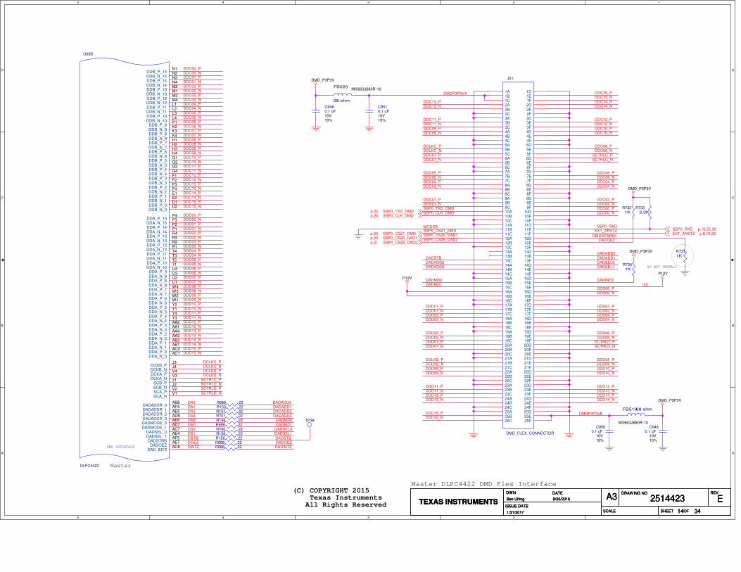
Master DLPC4422 DMD Flex Interface (C) COPYRIGHT 2015 Texas Instruments All Rights Reserved
Master
DMD_P3P3V
DMD_P3P3V
DMD_P3P3V
P12VP12V
DMD_P3P3V
SSP0_RXD p.16,25,30EXT_ARSTZ p.8,16,20
SSP0_TXD_DMDp.25SSP0_CLK_DMDp.25
SSP0_CSZ1_DMDp.25SSP0_CSZ0_DAD1p.25SSP0_CSZ5_DAD2p.21
TEXAS INSTRUMENTS
DWN DATE
ISSUE DATE
SCALE
DRAWING NO REV
SHEET OF
2514423 EA3
3414
Ben Uhing 9/30/2016
1/31/2017
TEXAS INSTRUMENTS
DWN DATE
ISSUE DATE
SCALE
DRAWING NO REV
SHEET OF
2514423 EA3
3414
Ben Uhing 9/30/2016
1/31/2017
TEXAS INSTRUMENTS
DWN DATE
ISSUE DATE
SCALE
DRAWING NO REV
SHEET OF
2514423 EA3
3414
Ben Uhing 9/30/2016
1/31/2017
R686 22
R699 22
DMD INTERFACE
U33B
DLPC4422
DDB_P_7H1
DDB_N_7H2
DDB_P_6H3
DDB_N_6H4
DDB_P_5G1
DDB_N_5G2
DDB_P_4G3
DDB_N_4G4
DDB_P_3F1
DDB_N_3F2
DDB_P_2F3
DDB_N_2F4
DDB_P_1E1
DDB_N_1E2
DDB_P_0D1
DDB_N_0D2
DDA_P_7W4
DDA_N_7W3
DDA_P_6W2
DDA_N_6W1
DDA_P_5Y2
DDA_N_5Y1
DDA_P_4Y4
DDA_N_4Y3
DDA_P_3AA2
DDA_N_3AA1
DDA_P_2AA4
DDA_N_2AA3
DDA_P_1AB2
DDA_N_1AB1
DDA_P_0AC2
DDA_N_0AC1
DCKB_PJ3
DCKB_NJ4
DCKA_PV4
DCKA_NV3
SCB_PJ1
SCB_NJ2
SCA_PV2
SCA_NV1
DDB_P_8K3
DDB_P_9K1
DDB_P_10L3
DDB_P_11L1
DDB_P_12M3
DDB_P_13M2
DDB_P_14N3
DDB_P_15N1
DDB_N_8K4
DDB_N_9K2
DDB_N_10L4
DDB_N_11L2
DDB_N_12M4
DDB_N_13M1
DDB_N_14N4
DDB_N_15N2
DDA_P_8U2
DDA_P_9U4
DDA_P_10T2
DDA_P_11T4
DDA_P_12R2
DDA_P_13R4
DDA_P_14P2
DDA_P_15P4
DDA_N_8U1
DDA_N_9U3
DDA_N_10T1
DDA_N_11T3
DDA_N_12R1
DDA_N_13R3
DDA_N_14P1
DDA_N_15P3
DADADDR_0AB8
DADADDR_1AF4
DADADDR_2AE5
DADADDR_3AD6
DADMODE_0AE6
DADMODE_1AD7
DADSEL_0AC7
DADSEL_1AE4
DADSTRBAF5
DADOEZAE7
DAD_INTZAC8
FB520
68 ohm
MI0603J680R-10
R700 22
C9510.1 uF10V10%
R689 22
R7311K
R153 22
R156 22
C9480.1 uF10V10%
FB51968 ohm
MI0603J680R-10
J51
DMD_FLEX_CONNECTOR
1A1B1C
1D1E1F
2C2B2A
3A3B3C
4B4A
4C5A5B5C6A6B6C7A7B7C
8C
13C
9A
10B
8B
12B
14B
9B
14A
11A
10A
11C
13B
12C
11B
12A
10C
14C
9C
13A
8A
15C
23C23B
20C
24A
16A
17B
15B
19B
21B
16B
21A
18A
17A
18C
20B
23A
19C
18B
19A
17C
24C
21C
16C
25A
24B
22C
22A22B
20A
15A
25B25C
12D
6E
12E
13F
18D18E
6F
21D
17F
25F
24E
7D
2D
9F
2E
9D
11E
9E
15D
22E
16D
7E
20E
15F
25E
14E
11D
16E
5D
3D2F
13E
8D
20F
23F
24F
23D
4E
21E
18F
22D
5F
12F
7F
4D
10D
4F
23E
11F
10F
22F
14D
24D
5E
17D
8F
3F
20D
25D
16F
17E
14F
13D
19D
8E
3E
19F19E
6D
15E
21F
10E
R151 22
C9500.1 uF
10V10%
R150 22
TP38
R7301K
R701 22
C9460.1 uF
10V10%
R7333.3K
R698 22
R7321K
R148 22
DDC13_PDDC13_N
DDC11_PDDC11_NDDC09_PDDC09_N
DCLKC_PDCLKC_NDDC07_PDDC07_N
DDC05_PDDC05_NDDC03_PDDC03_N
DDC01_PDDC01_NSSP0_TXD_DMDSSP0_CLK_DMD
MODEBSSP0_CSZ1_DMDSSP0_CSZ0_DAD1
DADSTBDADADD2
DADMD0DADMD1
DDD01_PDDD01_NDDD03_PDDD03_N
DDD05_PDDD05_NDDD07_PDDD07_N
DCLKD_PDCLKD_NDDD09_PDDD09_N
DDD11_PDDD11_NDDD13_PDDD13_N
DDD15_PDDD15_N
DADADD3
DDC15_PDDC15_NDDC14_PDDC14_N
DDC12_PDDC12_NDDC10_PDDC10_N
DDC08_PDDC08_N
SCTRLC_PSCTRLC_N
DDC06_PDDC06_NDDC04_PDDC04_N
DDC02_PDDC02_NDDC00_PDDC00_N
EXT_ARSTZ
DMDSPARE0DADOEZ
DADADD0DADADD1DADSEL0DADSEL1
DADINTZ12V
DDD00_PDDD00_N
DDD02_PDDD02_NDDD04_PDDD04_N
DDD06_PDDD06_N
SCTRLD_PSCTRLD_N
DDD08_PDDD08_NDDD10_PDDD10_N
DDD12_PDDD12_NDDD14_PDDD14_N
DMDP3P3VA
DMDP3P3VB
DADADD1DADADD2DADADD3
DADMD0DADMD1
DADSEL0DADSEL1DADSTBDADOEZDADINTZ
SSP0_CSZ5_DAD2
DA0DA1DA2
DM0DA3
DM1
DS1DS0
DSTB
DINTZDOEZ
SSP0_RXD
DADADD0
DCLKD_PDCLKD_N
DCLKC_PDCLKC_N
SCTRLD_PSCTRLD_N
SCTRLC_PSCTRLC_N
DDC00_PDDC00_NDDC01_PDDC01_NDDC02_PDDC02_NDDC03_PDDC03_NDDC04_PDDC04_NDDC05_PDDC05_NDDC06_PDDC06_NDDC07_PDDC07_NDDC08_PDDC08_NDDC09_PDDC09_NDDC10_PDDC10_NDDC11_PDDC11_NDDC12_PDDC12_NDDC13_PDDC13_NDDC14_PDDC14_NDDC15_PDDC15_N
DDD01_PDDD01_NDDD02_PDDD02_N
DDD00_NDDD00_P
DDD04_PDDD04_NDDD05_PDDD05_NDDD06_PDDD06_NDDD07_PDDD07_N
DDD09_PDDD09_NDDD10_PDDD10_NDDD11_PDDD11_NDDD12_PDDD12_NDDD13_PDDD13_NDDD14_PDDD14_NDDD15_PDDD15_N
DDD08_PDDD08_N
DDD03_PDDD03_N
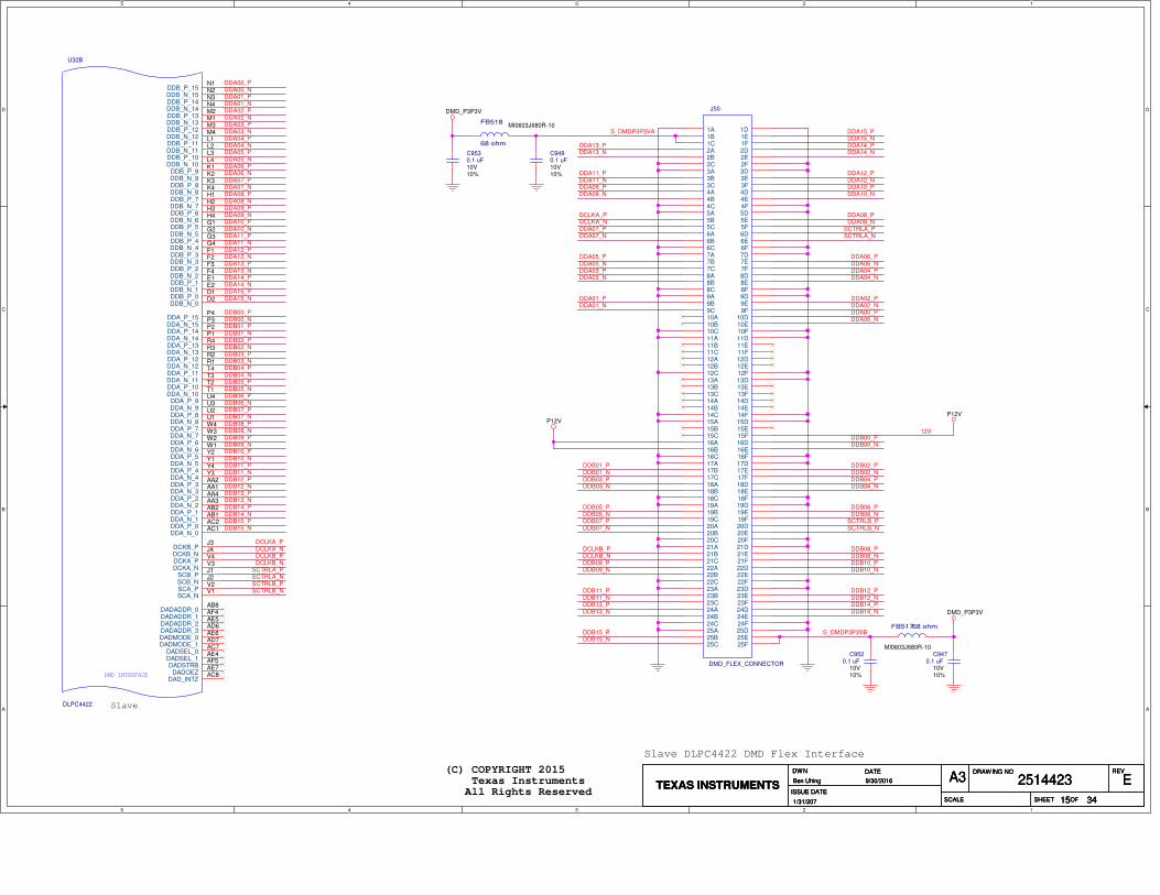
5
5
4
4
3
3
2
2
1
1
D D
C C
B B
A A
Slave DLPC4422 DMD Flex Interface
(C) COPYRIGHT 2015 Texas Instruments All Rights Reserved
Slave
DMD_P3P3V
P12VP12V
DMD_P3P3V
TEXAS INSTRUMENTS
DWN DATE
ISSUE DATE
SCALE
DRAWING NO REV
SHEET OF
2514423 EA3
3415
Ben Uhing 9/30/2016
1/31/207
TEXAS INSTRUMENTS
DWN DATE
ISSUE DATE
SCALE
DRAWING NO REV
SHEET OF
2514423 EA3
3415
Ben Uhing 9/30/2016
1/31/207
TEXAS INSTRUMENTS
DWN DATE
ISSUE DATE
SCALE
DRAWING NO REV
SHEET OF
2514423 EA3
3415
Ben Uhing 9/30/2016
1/31/207
FB51768 ohm
MI0603J680R-10
DMD INTERFACE
U32B
DLPC4422
DDB_P_7H1
DDB_N_7H2
DDB_P_6H3
DDB_N_6H4
DDB_P_5G1
DDB_N_5G2
DDB_P_4G3
DDB_N_4G4
DDB_P_3F1
DDB_N_3F2
DDB_P_2F3
DDB_N_2F4
DDB_P_1E1
DDB_N_1E2
DDB_P_0D1
DDB_N_0D2
DDA_P_7W4
DDA_N_7W3
DDA_P_6W2
DDA_N_6W1
DDA_P_5Y2
DDA_N_5Y1
DDA_P_4Y4
DDA_N_4Y3
DDA_P_3AA2
DDA_N_3AA1
DDA_P_2AA4
DDA_N_2AA3
DDA_P_1AB2
DDA_N_1AB1
DDA_P_0AC2
DDA_N_0AC1
DCKB_PJ3
DCKB_NJ4
DCKA_PV4
DCKA_NV3
SCB_PJ1
SCB_NJ2
SCA_PV2
SCA_NV1
DDB_P_8K3
DDB_P_9K1
DDB_P_10L3
DDB_P_11L1
DDB_P_12M3
DDB_P_13M2
DDB_P_14N3
DDB_P_15N1
DDB_N_8K4
DDB_N_9K2
DDB_N_10L4
DDB_N_11L2
DDB_N_12M4
DDB_N_13M1
DDB_N_14N4
DDB_N_15N2
DDA_P_8U2
DDA_P_9U4
DDA_P_10T2
DDA_P_11T4
DDA_P_12R2
DDA_P_13R4
DDA_P_14P2
DDA_P_15P4
DDA_N_8U1
DDA_N_9U3
DDA_N_10T1
DDA_N_11T3
DDA_N_12R1
DDA_N_13R3
DDA_N_14P1
DDA_N_15P3
DADADDR_0AB8
DADADDR_1AF4
DADADDR_2AE5
DADADDR_3AD6
DADMODE_0AE6
DADMODE_1AD7
DADSEL_0AC7
DADSEL_1AE4
DADSTRBAF5
DADOEZAE7
DAD_INTZAC8
C9520.1 uF
10V10%
C9470.1 uF
10V10%
FB518
68 ohm
MI0603J680R-10
J50
DMD_FLEX_CONNECTOR
1A1B1C
1D1E1F
2C2B2A
3A3B3C
4B4A
4C5A5B5C6A6B6C7A7B7C
8C
13C
9A
10B
8B
12B
14B
9B
14A
11A
10A
11C
13B
12C
11B
12A
10C
14C
9C
13A
8A
15C
23C23B
20C
24A
16A
17B
15B
19B
21B
16B
21A
18A
17A
18C
20B
23A
19C
18B
19A
17C
24C
21C
16C
25A
24B
22C
22A22B
20A
15A
25B25C
12D
6E
12E
13F
18D18E
6F
21D
17F
25F
24E
7D
2D
9F
2E
9D
11E
9E
15D
22E
16D
7E
20E
15F
25E
14E
11D
16E
5D
3D2F
13E
8D
20F
23F
24F
23D
4E
21E
18F
22D
5F
12F
7F
4D
10D
4F
23E
11F
10F
22F
14D
24D
5E
17D
8F
3F
20D
25D
16F
17E
14F
13D
19D
8E
3E
19F19E
6D
15E
21F
10E
C9490.1 uF10V10%
C9530.1 uF10V10%
S_DMDP3P3VB
S_DMDP3P3VA
DDA13_PDDA13_N
DDA11_PDDA11_NDDA09_PDDA09_N
DCLKA_PDCLKA_NDDA07_PDDA07_N
DDA05_PDDA05_NDDA03_PDDA03_N
DDA01_PDDA01_N
DDB01_PDDB01_NDDB03_PDDB03_N
DDB05_PDDB05_NDDB07_PDDB07_N
DCLKB_PDCLKB_NDDB09_PDDB09_N
DDB11_PDDB11_NDDB13_PDDB13_N
DDB15_PDDB15_N
DDA15_PDDA15_NDDA14_PDDA14_N
DDA12_PDDA12_NDDA10_PDDA10_N
DDA08_PDDA08_N
SCTRLA_PSCTRLA_N
DDA06_PDDA06_NDDA04_PDDA04_N
DDA02_PDDA02_NDDA00_PDDA00_N
12VDDB00_PDDB00_N
DDB02_PDDB02_NDDB04_PDDB04_N
DDB06_PDDB06_N
SCTRLB_PSCTRLB_N
DDB08_PDDB08_NDDB10_PDDB10_N
DDB12_PDDB12_NDDB14_PDDB14_N
DCLKB_PDCLKB_N
DCLKA_PDCLKA_N
SCTRLB_PSCTRLB_N
SCTRLA_PSCTRLA_N
DDA00_PDDA00_NDDA01_PDDA01_NDDA02_PDDA02_NDDA03_PDDA03_NDDA04_PDDA04_NDDA05_PDDA05_NDDA06_PDDA06_NDDA07_PDDA07_NDDA08_PDDA08_NDDA09_PDDA09_NDDA10_PDDA10_NDDA11_PDDA11_NDDA12_PDDA12_NDDA13_PDDA13_NDDA14_PDDA14_NDDA15_PDDA15_N
DDB00_PDDB00_NDDB01_PDDB01_NDDB02_PDDB02_NDDB03_PDDB03_NDDB04_PDDB04_NDDB05_PDDB05_NDDB06_PDDB06_NDDB07_PDDB07_NDDB08_PDDB08_NDDB09_PDDB09_NDDB10_PDDB10_NDDB11_PDDB11_NDDB12_PDDB12_NDDB13_PDDB13_NDDB14_PDDB14_NDDB15_PDDB15_N
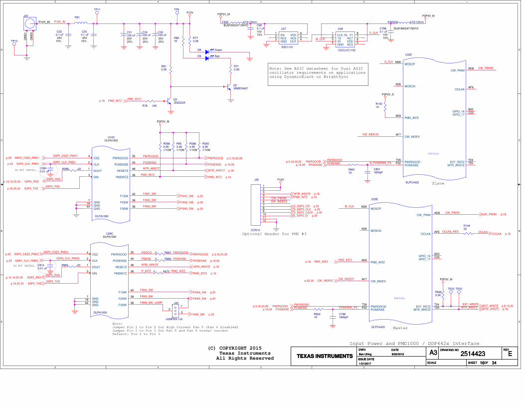
5
5
4
4
3
3
2
2
1
1
D D
C C
B B
A A
Input Power and PMD1000 / DDP442x Interface (C) COPYRIGHT 2015 Texas Instruments All Rights Reserved
Note:Jumper Pin 1 to Pin 2 for High Current Fan 5 (Fan 6 Disabled)Jumper Pin 2 to Pin 3 for Fan 5 and Fan 6 normal currentDefault: Pin 2 to Pin 3
Master
Slave
Note: See ASIC datasheet for Dual ASICoscillator requirements on applicationsusing DynamicBlack or BrightSync
DO NOT INSTALL
DO NOT INSTALL
Optional Header for PMD #3
P3P3V_M
P12V
P3P3V_M
P3P3V_S
P3P3V_MP3P3V_M
P12VSSP0_RXDp.14,16,25,30
SSP0_CLK_PMD1p.25
SSP0_TXDp.16,25,30
PWRGOOD p.3,16,23,26
POSENSE p.16,26
SSP0_CSZ2_PMD1p.25
FAN1_SW p.20
CW_INDEX1p.20,30
FAN2_SW p.20
FAN3_SW p.20
PWRGOODp.3,16,23,26POSENSEp.16,26
OCLKA p.19
CW_PWM1 p.19
EXT_ARSTZ p.8,14,20MTR_ARSTZ p.16
MTR_ARSTZ p.16
PMD_INTZp.16
PMD_INTZ p.16
PMD_INTZp.16
SSP0_RXDp.14,16,25,30
SSP0_CLK_PMD2p.25
SSP0_TXDp.16,25,30
PWRGOOD p.3,16,23,26
POSENSE p.16,26
SSP0_CSZ3_PMD2p.25
FAN4_SW p.20
FAN5_SW p.20
FAN6_SW p.20
PMD_INTZ p.16
MTR_ARSTZ p.16
PWRGOODp.3,16,23,26POSENSEp.16,26
PMD_INTZ p.16MTR_ARSTZ p.16
S_SSP2_DO p.30S_SSP2_CLK p.30S_SSP2_CSZ0 p.30S_SSP2_DI p.30
TEXAS INSTRUMENTS
DWN DATE
ISSUE DATE
SCALE
DRAWING NO REV
SHEET OF
2514423 EA3
3416
Ben Uhing 9/30/2016
1/31/2017
TEXAS INSTRUMENTS
DWN DATE
ISSUE DATE
SCALE
DRAWING NO REV
SHEET OF
2514423 EA3
3416
Ben Uhing 9/30/2016
1/31/2017
TEXAS INSTRUMENTS
DWN DATE
ISSUE DATE
SCALE
DRAWING NO REV
SHEET OF
2514423 EA3
3416
Ben Uhing 9/30/2016
1/31/2017
U10C
DLPA1000
DLPA1000
PWRGOOD35
RESETZ48
POSENSE34
PMDINTZ36
CSZ4
CLK2
DOUT1
DIN3
F1SW40
F2SW39
F3SW38
GND7
GND19
GND44
R6700
R801K
R6611K
+ C51100 uF
20%25V
R5933.3K1/10W
C8140.01 uF
J30
CON12
123456789101112
R6660
C950.1 uF10V10%
R665 22
R78 10K
+C24100 uF
20%25V
U27
DSC1101
EN1
NC22
GND3
OUT4NC55VDD6
R773.3K
TP23
C7980.1 uF
10V10%
DDP442x
U33E
DLPC4422
GPIO_16B23
GPIO_17C22
MOSCPM26
MOSCNN26
POSENSEP22 PWRGOODT26
MTR_ARSTZT25EXT_RSTZT24
CW_PWMAD8
PMD_INTZAE8
CW_INDEXAF7
OCLKAAF6
J22
P12V_ING
ND
1
GN
D2
TP9
FB1
TP22
Q2MMBT6427
J40
JUMPER-1x3
12
3
R14433
R6463.3K
FB2 470 OhmBLM18AG471SN1D
R713.3K
C250.1 uF25V
10%
U28
CDCLVC1102
CLK_IN1
1G2
Y03
GND4
NC55VDD6NC77Y18
Q32N2222A
FB503 470 Ohm
BLM18AG471SN1D
D9 Red
R953.3K1/10W
C7991800pF
TP11
R813.3K
C5840.01 uF
C220.1 uF25V
10%
U29C
DLPA1000
DLPA1000
PWRGOOD35
RESETZ48
POSENSE34
PMDINTZ36
CSZ4
CLK2
DOUT1
DIN3
F1SW40
F2SW39
F3SW38
GND7
GND19
GND44
TP12
R5983.3K1/10W
R586 22
DDP442x
U32E
DLPC4422
GPIO_16B23
GPIO_17C22
MOSCPM26
MOSCNN26
POSENSEP22 PWRGOODT26
MTR_ARSTZT25EXT_RSTZT24
CW_PWMAD8
PMD_INTZAE8
CW_INDEXAF7
OCLKAAF6
R5883.3K1/10W
D8 Green
C8011800pF
+C50100 uF
20%25V
R1421K
R6670
R6521K
POSENSE
PMD_INTZ
SSP0_CSZ2_PMD1
SSP0_CLK_PMD1
SSP0_TXD
POSENSE_FIL
CW_INDEX1
PWRGOODPOSENSE
MTR_ARSTZ
P12V_IN
PMD_INTZ
PWRGOOD
PMD_INTZ
FAN1_SW
FAN2_SW
FAN3_SW
OCLKA_RES OCLKA
CW_PWM1
MTR_ARSTZ
SSP0_RXD
EXT_ARSTZ
SSP0_CSZ3_PMD2
SSP0_CLK_PMD0
SSP0_TXD
POSENSE
MTR_ARSTZ
PMD_INTZ
PWRGOOD
FAN4_SW
FAN6_SW_JUMP
FAN5_SW
PGOOD
P_INTZ
PSENS
SSP0_RXD
PWRGOODS_POSENSE_FILPOSENSE
S_CLK
M_CLK
M_CLK
S_CLK
CW_PWM3CW_INDEX3
CW_INDEX3
CW_PWM3
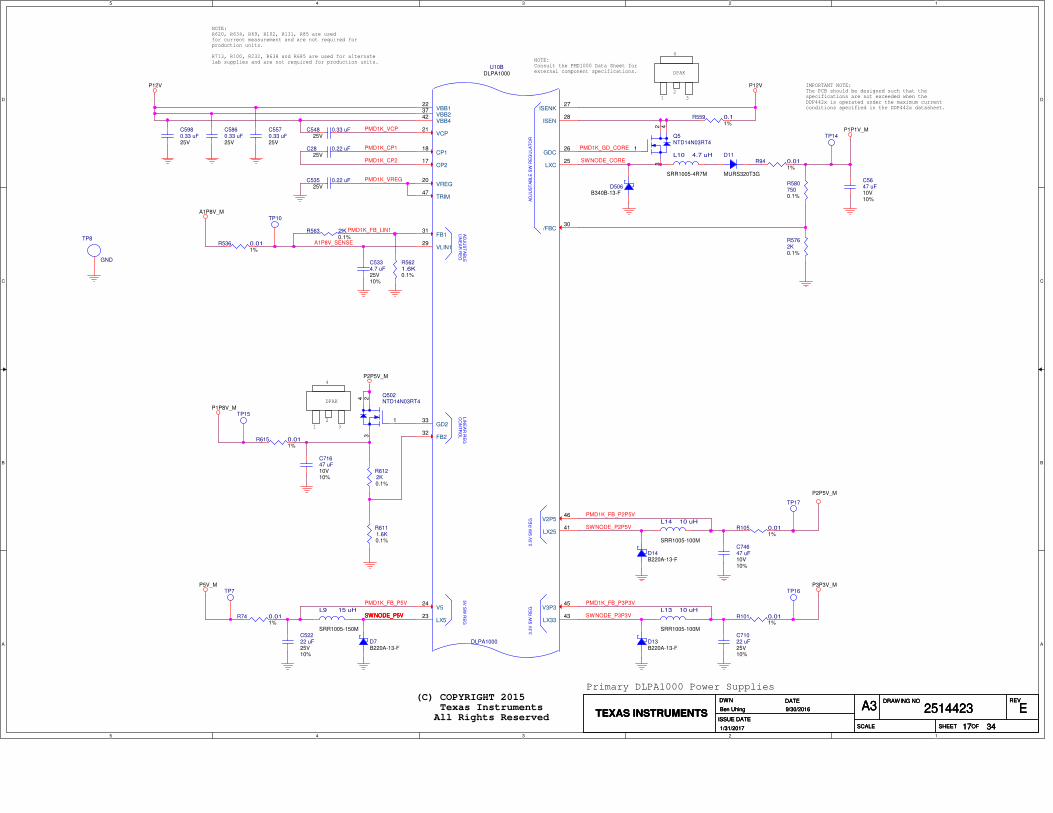
5
5
4
4
3
3
2
2
1
1
D D
C C
B B
A A
DPAK
1
2
3
4
NOTE:R620, R634, R69, R102, R131, R85 are used for current measurement and are not required for production units.
R713, R100, R232, R638 and R685 are used for alternate lab supplies and are not required for production units. NOTE:
Consult the PMD1000 Data Sheet for external component specifications.
IMPORTANT NOTE:The PCB should be designed such that the specifications are not exceeded when the DDP442x is operated under the maximum currentconditions specified in the DDP442x datasheet.
DPAK
Primary DLPA1000 Power Supplies
1
2
3
4
(C) COPYRIGHT 2015 Texas Instruments All Rights Reserved
A1P8V_M
P1P1V_M
P2P5V_M
P1P8V_M
P12VP12V
P3P3V_MP5V_M
P2P5V_M
TEXAS INSTRUMENTS
DWN DATE
ISSUE DATE
SCALE
DRAWING NO REV
SHEET OF
2514423 EA3
3417
Ben Uhing 9/30/2016
1/31/2017
TEXAS INSTRUMENTS
DWN DATE
ISSUE DATE
SCALE
DRAWING NO REV
SHEET OF
2514423 EA3
3417
Ben Uhing 9/30/2016
1/31/2017
TEXAS INSTRUMENTS
DWN DATE
ISSUE DATE
SCALE
DRAWING NO REV
SHEET OF
2514423 EA3
3417
Ben Uhing 9/30/2016
1/31/2017
L14 10 uH
SRR1005-100M
D506B340B-13-F
D13B220A-13-F
Q502NTD14N03RT4
1
243
TP8
GND
C5860.33 uF25V
R5621.6K0.1%
C535 0.22 uF25V
TP14
R6122K0.1%
C5570.33 uF25V
TP7
C74647 uF10V10%
R94 0.011%
R536 0.011%
TP16
C5647 uF10V10%
R101 0.011%
R6111.6K0.1%
Q5NTD14N03RT4
1
2 43
C28 0.22 uF25V
R105 0.011%
R5807500.1%
C5334.7 uF25V10%
L9 15 uH
SRR1005-150M
AD
JU
ST
AB
LE
LIN
EA
R R
EG
5V
SW
RE
GLIN
EA
R R
EG
CO
NT
RO
L
3.3
V S
W R
EG
2.5
V S
W R
EG
AD
JU
ST
AB
LE
SW
RE
GU
LA
TO
R
U10B
DLPA1000
DLPA1000
VBB122
VBB237
VBB442
VCP21
CP118
CP217
VREG20
TRIM47
ISENK27
ISEN28
GDC26
LXC25
/FBC30
V2P546
LX2541
V3P345
LX3343
V524
LX523
FB131
VLIN129
GD233
FB232
D14B220A-13-F
C52222 uF25V10%
TP17
R563 2K0.1%
R615 0.011%
C548 0.33 uF25V
R74 0.011%
TP15
C71022 uF25V10%
C71647 uF10V10%
D11
MURS320T3G
TP10
D7B220A-13-F
R559 0.11%
L10 4.7 uH
SRR1005-4R7M
L13 10 uH
SRR1005-100M
C5980.33 uF25V
R5762K0.1%
PMD1K_FB_LIN1
A1P8V_SENSE
PMD1K_VCP
PMD1K_CP1
SWNODE_COREPMD1K_CP2
PMD1K_FB_P5V
SWNODE_P5VSWNODE_P5VSWNODE_P5VSWNODE_P5V
PMD1K_FB_P3P3V
PMD1K_VREG
SWNODE_P3P3V
PMD1K_GD_CORE
PMD1K_FB_P2P5V
SWNODE_P2P5V

5
5
4
4
3
3
2
2
1
1
D D
C C
B B
A A
NOTE:Consult the PMD1000 Data Sheet for external component specifications.
IMPORTANT NOTE:The PCB should be designed such that the specifications are not exceeded when the DDP442x is operated under the maximum currentconditions specified in the DDP442x datasheet.
DPAK
1
2
3
4
1
2
DPAK
3
4
Secondary DLPA1000 Supplies (C) COPYRIGHT 2015 Texas Instruments All Rights Reserved
NOTE:R587, R525, R46, R576, R14 are used for current measurement and are not required for production units.
DO NOT INSTALL
P12V
P1P1V_S
P12V
P2P5V_S
P1P8V_S
P2P5V_S
P3P3V_S
A1P8V_S
P3P3V_M
P12V
P12V
DMD_P3P3V
P5V_S
TEXAS INSTRUMENTS
DWN DATE
ISSUE DATE
SCALE
DRAWING NO REV
SHEET OF
2514423 EA3
3418
Ben Uhing 9/30/2016
1/31/2017
TEXAS INSTRUMENTS
DWN DATE
ISSUE DATE
SCALE
DRAWING NO REV
SHEET OF
2514423 EA3
3418
Ben Uhing 9/30/2016
1/31/2017
TEXAS INSTRUMENTS
DWN DATE
ISSUE DATE
SCALE
DRAWING NO REV
SHEET OF
2514423 EA3
3418
Ben Uhing 9/30/2016
1/31/2017
C795 0.33 uF25V
AD
JU
ST
AB
LE
LIN
EA
R R
EG
5V
SW
RE
GLIN
EA
R R
EG
CO
NT
RO
L
3.3
V S
W R
EG
2.5
V S
W R
EG
AD
JU
ST
AB
LE
SW
RE
GU
LA
TO
R
U29B
DLPA1000
DLPA1000
VBB122
VBB237
VBB442
VCP21
CP118
CP217
VREG20
TRIM47
ISENK27
ISEN28
GDC26
LXC25
/FBC30
V2P546
LX2541
V3P345
LX3343
V524
LX523
FB131
VLIN129
GD233
FB232
TP36
R727
10K
C89947 uF10V10%
C11747 pF
C88047 uF10V10%
C1110.01 uF
L18 4.7 uH
SRR1005-4R7M
Q6NTD14N03RT4
1
2 43
TP20
R157 0.011%
Q503NTD14N03RT4
1
243
R18129.4K
D507B220A-13-F
R638 0.011%
C89 0.22 uF25V
TP31
D20B220A-13-F
R723
10K
TP39
R18410.2K
R6501.6K0.1%
R1850
TP21
GND
C789 0.22 uF25V
R7200
D23B340B-13-F
C9847 uF10V10%
R137 0.011%
C8150.33 uF25V
C9454.7 uF
R6782K0.1%
R1693.24K
C87522 uF25V10%
L22 6.8 uH
L16 15 uH
SRR1005-150M
C8160.33 uF25V
D17
MURS220T3G
C7884.7 uF25V10%
U38
TPS54331
BOOT1
VIN2
EN3
SS4
VSNS5COMP6GND7PH8
C1130.1 uF25V
10%
R6771.6K0.1%
C11447 uF
C77922 uF25V10%
R183 0.011%
C1054.7 uF
C7970.33 uF25V
L20 10 uH
SRR1005-100M
C11547 uF
Q5052N2222A
R647 0.11%
C1064.7 uF
R651 2K0.1%
R6637500.1%
Q5042N2222A
R112 0.011%
D19B220A-13-F
L21 10 uH
SRR1005-100M
R681 0.011%
C1070.01 uF
TP25
R143 0.011%
R6622K0.1%
C1181000 pF
D16B220A-13-F
TP35
PMD1K2_VCP
PMD1K2_CP1
PMD1K2_CP2
PMD1K2_VREG
SWNODE2_CORE
PMD1K2_GD_CORE
PMD1K2_FB_P2P5V
SWNODE2_P2P5V
PMD1K2_FB_P3P3V
SWNODE2_P3P3V
PMD1K2_FB_LIN1
A1P8V2_SENSE
SW_EN
SW_SS
SW_PH
SW_BOOT
SW_VOUT
SW_COMP
SW_VSNS
PMD1K2_FB_P5V
SWNODE2_P5V
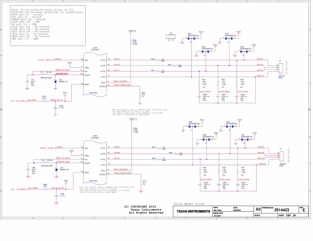
5
5
4
4
3
3
2
2
1
1
D D
C C
B B
A A
SOT-323
1 2
3
NOTE: This resistor value is dependant upon the CW motor used. The value range is 0.47 ohms to 2.2 ohms. The target vlotage range for the SENSE pin is 100-150mV when the CW is running at a stable speed.
NOTE: This resistor value is dependant upon the CW motor used. The value range is 0.47 ohms to 2.2 ohms. The target vlotage range for the SENSE pin is 100-150mV when the CW is running at a stable speed.
Color Wheel Drive (C) COPYRIGHT 2015 Texas Instruments All Rights Reserved
CW1 MOTOR DRIVE
CW2 MOTOR DRIVE
Note: If not using the motor driver on the DLPA1000 follow these guidelines for unused pins:GMIN (pin 8) – GroundOSC (pin 6) – GroundSENSE (pin 14) – GroundCTAP (pin 13) – VBBVM (pin 11) – VBBOUTA (pin 12) – No ConnectOUTB (pin 15) – No ConnectOUTC (pin 16) – No ConnectTACH (pin 5) – No ConnectVMSW (pin 10) – No ConnectVBB (pin 37) – VBB
P12V
P3P3V_MP12V P12V
P12VP12V
P12V
P3P3V_SP12V P12V
P12VP12V
OCLKAp.16,19
CW_PWM1p.16
OCLKAp.16,19
CW_PWM2p.21
TEXAS INSTRUMENTS
DWN DATE
ISSUE DATE
SCALE
DRAWING NO REV
SHEET OF
2514423 EA3
3419
Ben Uhing 9/30/2016
1/31/2017
TEXAS INSTRUMENTS
DWN DATE
ISSUE DATE
SCALE
DRAWING NO REV
SHEET OF
2514423 EA3
3419
Ben Uhing 9/30/2016
1/31/2017
TEXAS INSTRUMENTS
DWN DATE
ISSUE DATE
SCALE
DRAWING NO REV
SHEET OF
2514423 EA3
3419
Ben Uhing 9/30/2016
1/31/2017
R6643.3K1/10W
D18B220A-13-F
J2
MOLEXCON4
1234
DN4BAT54SWT1G
1 2
3
R35
150
1/4W
5%
R1172.21%R660
10K
R30 01/8W
R28
150
1/4W
5%
U10A
DLPA1000
DLPA1000
OSC6
VBB39
VM11
VMSW10
GMIN8
OUTA12
OUTB15
OUTC16
CTAP13
TACH5
SENSE14
R33
150
1/4W
5%
DN2BAT54SWT1G
1 2
3
R32 01/8W
C5080.001 uF50V10%
C5560.1 uF
DN8BAT54SWT1G
1 2
3
DN1BAT54SWT1G
1 2
3
R31 01/8W
J1
MOLEXCON4
1234
C5070.001 uF50V10%
TP13
DN3BAT54SWT1G
1 2
3
R27
150
1/4W
5%
L11 33 uH
SRR1005-330Y
R24 01/8W
DN6BAT54SWT1G
1 2
3
C5090.001 uF50V10%
R29
150
1/4W
5%
C2722 uF25V10%
R26 01/8W
DN7BAT54SWT1G
1 2
3
R5833.3K1/10W
C5040.001 uF50V10%
D12B220A-13-F
R25 01/8W
DN5BAT54SWT1G
1 2
3
C7960.1 uF
C5030.001 uF50V10%
R832.21%
U29A
DLPA1000
DLPA1000
OSC6
VBB39
VM11
VMSW10
GMIN8
OUTA12
OUTB15
OUTC16
CTAP13
TACH5
SENSE14
TP28
L19 33 uH
SRR1005-330Y
R57410K
C5050.001 uF50V10%
C8822 uF25V10%
R34
150
1/4W
5%
OUT1A_SNUB
PMD1K_FB_MOT1 CWY1C
CWY1B
CWY1A
PMD1K_GM_IN1CW_PWM1
OUT1A
OUT1B
CWCTR1
OUT1C
REAL_CWTACH1
PMD1K_SENSE_MOT1
OUT1C_SNUB OUT1B_SNUB
OCLKA
SWNODE_MOTSWNODE_MOT1
OUT2A_SNUB
PMD1K_FB_MOT2 CWY2C
CWY2B
CWY2A
PMD1K_GM_IN2CW_PWM2
OUT2A
OUT2B
CWCTR2
OUT2C
REAL_CWTACH2
PMD1K_SENSE_MOT2
OUT2C_SNUB OUT2B_SNUB
OCLKA
SWNODE_MOT2
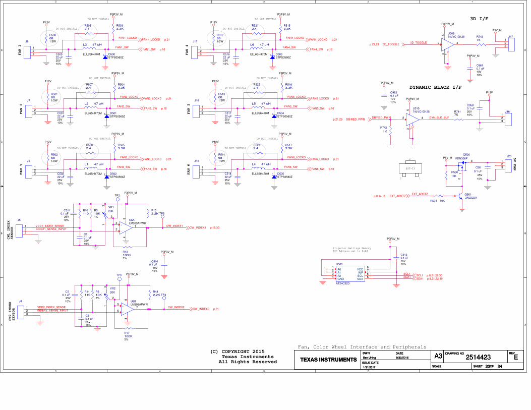
5
5
4
4
3
3
2
2
1
1
D D
C C
B B
A A
FAN 1
DO NOT INSTALL
DO NOT INSTALL
Fan, Color Wheel Interface and Peripherals
CW1 INDEX
SENSOR
5V FAN
FAN 2
DO NOT INSTALL
DO NOT INSTALL
FAN 3
DO NOT INSTALL
DO NOT INSTALL
FAN 4
DO NOT INSTALL
DO NOT INSTALL
FAN 5
DO NOT INSTALL
DO NOT INSTALL
FAN 6
DO NOT INSTALL
DO NOT INSTALL
CW2 INDEX
SENSOR
DYNAMIC BLACK I/F
3D I/F
(C) COPYRIGHT 2015 Texas Instruments All Rights Reserved
12
3
SOT-23
Projector Settings MemoryI2C Address set to 0xA8
P12V
P3P3V_M
P3P3V_M
P12V
P3P3V_M
P12V
P3P3V_M
P12V
P3P3V_M
P12V
P3P3V_M
P12V
P3P3V_M
P3P3V_M
P3P3V_M
P12V
P3P3V_M
P3P3V_M
P3P3V_M
P3P3V_M
P5V_M
P5V_M
P3P3V_M
FAN1_SW p.16
FAN1_LOCKD p.21
CW_INDEX1 p.16,30
FAN2_SW p.16
FAN2_LOCKD p.21
FAN3_SW p.16
FAN3_LOCKD p.21
FAN4_SW p.16
FAN4_LOCKD p.21
FAN5_SW p.16
FAN5_LOCKD p.21
FAN6_SW p.16
FAN6_LOCKD p.21
CW_INDEX2 p.21
DB/RED_PWMp.21,29
3D_TOGGLEp.21,29
EXT_ARSTZp.8,14,16
SDA1 p.8,21,22,30SCL1 p.8,21,22,30
TEXAS INSTRUMENTS
DWN DATE
ISSUE DATE
SCALE
DRAWING NO REV
SHEET OF
2514423 EA3
3420
Ben Uhing 9/30/2016
1/31/2017
TEXAS INSTRUMENTS
DWN DATE
ISSUE DATE
SCALE
DRAWING NO REV
SHEET OF
2514423 EA3
3420
Ben Uhing 9/30/2016
1/31/2017
TEXAS INSTRUMENTS
DWN DATE
ISSUE DATE
SCALE
DRAWING NO REV
SHEET OF
2514423 EA3
3420
Ben Uhing 9/30/2016
1/31/2017
C51822 uF25V10%
D502STPS0560Z
C5130.1 uF10V10%
D501STPS0560Z
D500STPS0560Z
J8
123
Q5012N2222A
R17100K5%
R152.2K
L4 47 uH
ELL6SH470M
R74175
R510K1%
R5062.4
L6 47 uH
ELL6SH470M
U50974LVC1G125
2 4
513
TP5
C50222 uF25V10%
R11110
J46123
J15
123
C50122 uF25V10%
R5153.3K
J17
123
C51722 uF25V10%
L3 47 uH
ELL6SH470M
J47123
J20
123
R5173.3K
R610K5%
VR2
20K
13
2
R74375
Q500
FDN306P
12
3
R5033.3K
J4
123
U51074LVC1G125
2 4
513
R5212.4
C20.1 uF25V10%
R530
10K
R512681/2W
L1 47 uH
ELL6SH470M
R5232.4
R182.2K
L2 47 uH
ELL6SH470M
J16
123
L5 47 uH
ELL6SH470M
C50022 uF25V10%
R514681/2W
+
-
U6BLM393APWR5
7
84
6
R500681/2W
C50.1 uF
25V10%
R5053.3K
J6
123
C10.1 uF25V10%
C26
0.1 uF
25V
10%
R5043.3K
J7
123
C9620.1 uF10V10%
R10110
R534 10K
TP4
R5163.3K
TP3
D505STPS0560Z
D503STPS0560Z
R5082.4
C9610.1 uF10V10%
R502681/2W
R5072.4
R501681/2W
VR1
20K
13
2
C9580.1 uF25V10%
R513681/2W
C5100.1 uF
10V10%
R13100K5%
R742
1K
U500
AT24C32D
A01
A12
A23
GND4
SDA5SCL6WP7VCC8
R5222.4
C5110.1 uF
25V10%
TP2
C51622 uF25V10%
+
-
U6ALM393APWR3
1
84
2
J5
123
D504STPS0560Z
FAN1_SW
CW_INDEX1
FAN1_LOCKD
VDD1_INDEX_SENSE
FAN2_SW
FAN2_LOCKD
FAN3_SW
FAN3_LOCKD
FAN4_SW
FAN4_LOCKD
FAN5_SW
FAN5_LOCKD
FAN6_SW
FAN6_LOCKD
INDEX1_SENSE_INPUT
CW_INDEX2VDD2_INDEX_SENSEINDEX2_SENSE_INPUT
DB/RED_PWM DYN_BLK_BUF
3D_TOGGLE
EXT_ARSTZ
SCL1SDA1
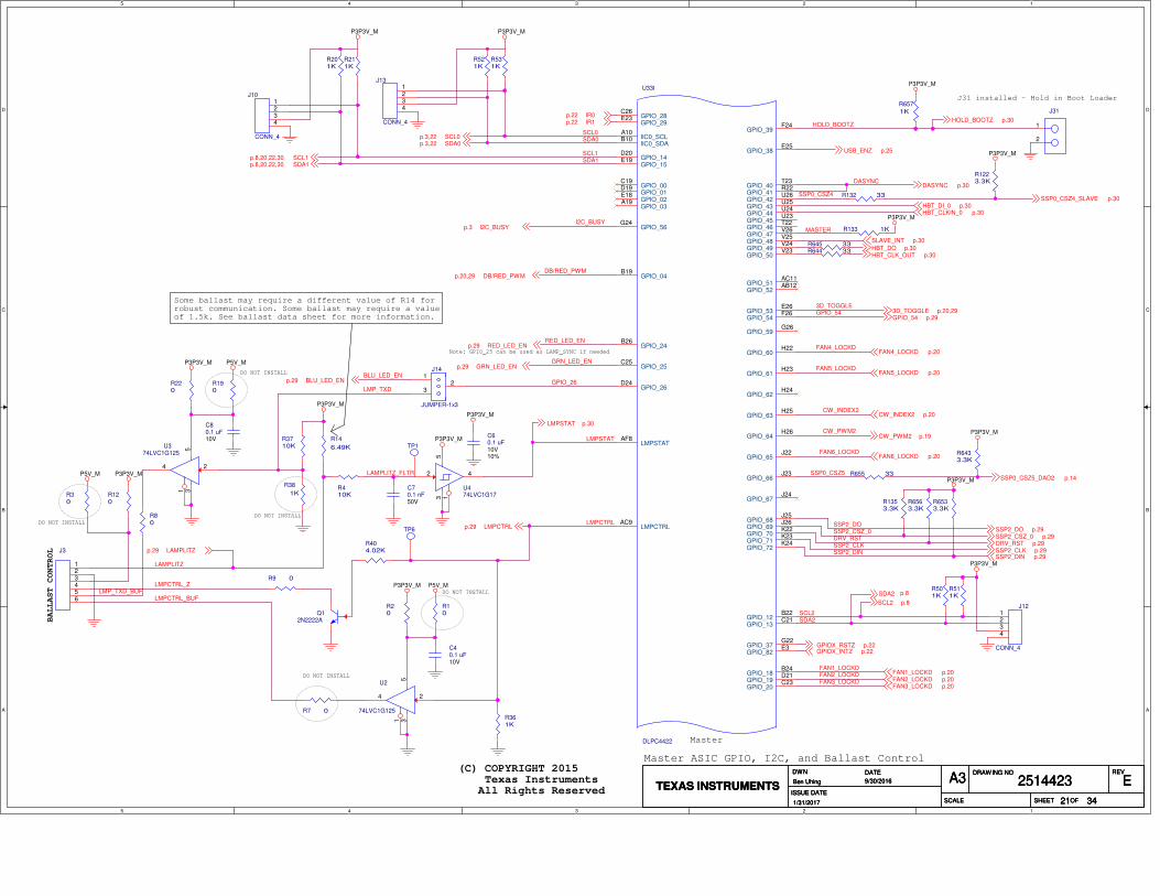
5
5
4
4
3
3
2
2
1
1
D D
C C
B B
A A
DO NOT INSTALL
BALLAST CONTROL
DO NOT INSTALL
DO NOT INSTALL
DO NOT INSTALL
DO NOT INSTALL
Note: GPIO_25 can be used as LAMP_SYNC if needed
Master ASIC GPIO, I2C, and Ballast Control (C) COPYRIGHT 2015 Texas Instruments All Rights Reserved
J31 installed - Hold in Boot Loader
Master
Some ballast may require a different value of R14 forrobust communication. Some ballast may require a valueof 1.5k. See ballast data sheet for more information.
P3P3V_M
P5V_M
P5V_M
P5V_M
P3P3V_M
P3P3V_M
P3P3V_M
P3P3V_M
P3P3V_M
P3P3V_M
P3P3V_M
P3P3V_M
P3P3V_M
P3P3V_M
P3P3V_M
P3P3V_M
P3P3V_M
SCL0p.3,22SDA0p.3,22
RED_LED_ENp.29
GRN_LED_ENp.29
CW_INDEX2 p.20
SSP2_DO p.29SSP2_CSZ_0 p.29DRV_RST p.29
FAN1_LOCKD p.20FAN2_LOCKD p.20FAN3_LOCKD p.20
USB_ENZ p.25
3D_TOGGLE p.20,29
CW_PWM2 p.19
SSP0_CSZ5_DAD2 p.14
DASYNC p.30
DB/RED_PWMp.20,29
BLU_LED_ENp.29
FAN5_LOCKD p.20
FAN4_LOCKD p.20
GPIO_54 p.29
FAN6_LOCKD p.20
SSP2_CLK p.29SSP2_DIN p.29
LMPCTRLp.29
LAMPLITZp.29
HBT_CLK_OUT p.30HBT_DO p.30
HBT_DI_0 p.30HBT_CLKIN_0 p.30
I2C_BUSYp.3
SSP0_CSZ4_SLAVE p.30
SCL1p.8,20,22,30SDA1p.8,20,22,30
SLAVE_INT p.30
LMPSTAT p.30
HOLD_BOOTZ p.30
GPIOX_RSTZ p.22GPIOX_INTZ p.22
IR0p.22IR1p.22
SDA2 p.8
SCL2 p.8
TEXAS INSTRUMENTS
DWN DATE
ISSUE DATE
SCALE
DRAWING NO REV
SHEET OF
2514423 EA3
3421
Ben Uhing 9/30/2016
1/31/2017
TEXAS INSTRUMENTS
DWN DATE
ISSUE DATE
SCALE
DRAWING NO REV
SHEET OF
2514423 EA3
3421
Ben Uhing 9/30/2016
1/31/2017
TEXAS INSTRUMENTS
DWN DATE
ISSUE DATE
SCALE
DRAWING NO REV
SHEET OF
2514423 EA3
3421
Ben Uhing 9/30/2016
1/31/2017
R14
6.49K
R531K
R511K
J31
1
2
C60.1 uF10V10%
C80.1 uF10V R37
10K
R657
1K
R521K
U474LVC1G17
2 4
513
J14
JUMPER-1x3
12
3
R80
R132 33
J3
123456
TP1
R361K
R9 0
R38
1K
R1223.3K
TP6
R133 1K
R410K
R645 33
R30
R211K
R6563.3K
R6433.3K
R7 0
R120
R20
J12
CONN_4
1234
R201K
R404.02K
U2
74LVC1G125
24
51 3
U33I
DLPC4422
GPIO_28C26
GPIO_29E23
IIC0_SCLA10
IIC0_SDAB10
GPIO_00C19
GPIO_01D19
GPIO_02E18
GPIO_03A19
GPIO_14D20
GPIO_15E19
GPIO_39F24
GPIO_38E25
GPIO_37G22
GPIO_18B24
GPIO_19D21
GPIO_20C23
GPIO_12B22
GPIO_13C21
GPIO_24B26
GPIO_25C25
GPIO_26D24
LMPSTATAF8
LMPCTRLAC9
GPIO_40T23
GPIO_41R22
GPIO_42U26
GPIO_43U25
GPIO_44U24
GPIO_45U23
GPIO_46T22
GPIO_47V26
GPIO_48V25
GPIO_49V24
GPIO_50V23
GPIO_51AC11
GPIO_52AB12
GPIO_53E26
GPIO_54F26
GPIO_56G24
GPIO_59G26
GPIO_60H22
GPIO_61H23
GPIO_62H24
GPIO_63H25
GPIO_64H26
GPIO_65J22
GPIO_66J23
GPIO_67J24
GPIO_68J25
GPIO_69J26
GPIO_70K22
GPIO_71K23
GPIO_72K24
GPIO_82E3
GPIO_04B19
R6533.3K
J10
CONN_4
1234
R655 33
R644 33
R10
U374LVC1G125
24
51 3
Q12N2222A
C40.1 uF10V
J13
CONN_4
1234
C70.1 nF50V
R220
R501K
R190
R1353.3K
SCL0SDA0
I2C_BUSY
LMPSTAT
LMPCTRL
FAN3_LOCKDFAN2_LOCKDFAN1_LOCKD
GPIO_54
LMPCTRL_BUF
LMPCTRL_ZLMP_TXD_BUF
LAMPLITZ_FLTR
GRN_LED_EN
RED_LED_EN
CW_INDEX2
SSP2_DO
CW_PWM2
HOLD_BOOTZ
DB/RED_PWM
3D_TOGGLE
SDA2SCL2
GPIO_26BLU_LED_EN
LMP_TXD
FAN5_LOCKD
FAN4_LOCKD
FAN6_LOCKD
LAMPLITZ
SSP0_CSZ4
SSP0_CSZ5
DASYNC
SCL1
MASTER
SSP2_DINSSP2_CLKDRV_RSTSSP2_CSZ_0
SDA1

5
5
4
4
3
3
2
2
1
1
D D
C C
B B
A A
KEYBOARD INTERFACE
DO NOT INSTALL
(C) COPYRIGHT 2015 Texas Instruments All Rights Reserved
GPIO Expander, Keypad Interface and IR Interface
Master
DO NOT INSTALL
P3P3V_M
P3P3V_M
P3P3V_M
P3P3V_MP3P3V_M
P3P3V_M
P3P3V_M
P3P3V_M
IR0p.21
IR1p.21
GPIOX_RSTZp.21
SDA1p.8,20,21,30SCL1p.8,20,21,30
GPIOX_INTZ p.21
SSP1_DI p.8SSP1_CLK p.8SSP1_DO p.8SSP1_CSZ_0 p.8
PROG_FLASH_IN p.8
SDA0p.3,21SCL0p.3,21
TEXAS INSTRUMENTS
DWN DATE
ISSUE DATE
SCALE
DRAWING NO REV
SHEET OF
2514423 EA3
3422
Ben Uhing 9/30/2016
1/31/2017
TEXAS INSTRUMENTS
DWN DATE
ISSUE DATE
SCALE
DRAWING NO REV
SHEET OF
2514423 EA3
3422
Ben Uhing 9/30/2016
1/31/2017
TEXAS INSTRUMENTS
DWN DATE
ISSUE DATE
SCALE
DRAWING NO REV
SHEET OF
2514423 EA3
3422
Ben Uhing 9/30/2016
1/31/2017
D4Red
R658 22
R54
1K
R69
1K
POINTBLANK INTERFACE
U33D
DLPC4422
GPIO_30D25
GPIO_31F22
GPIO_32E24GPIO_33D26
GPIO_34F23
GPIO_57F25
GPIO_79AE9
GPIO_80AD9
GPIO_81AB10
J18CON14
1234567891011121314
D6Red
R67 0
R45 220
R561K
R188 0
U8
TCA8418
VCC21
RESETZ20
SDA22
SCL23
GND19
GPIOx_001
GPIOx_012
GPIOx_023
GPIOx_034
GPIOx_045
GPIOx_056
GPIOx_067
GPIOx_078
GPIOx_089
GPIOx_0910
GPIOx_1011
GPIOx_1112
GPIOx_1213
GPIOx_1314
GPIOx_1415GPIOx_1516GPIOx_1617GPIOx_1718
INTZ24
PAD25
R63
1K
U44IR_RECVR
123
R659 22
R641K
R68 0
R189 0
R187335%
D21
Red
R49 220
R16335%
R6533
R683 220
R44 220
C180.1 uF10V10%
C34.7 uF
25V
R58
1K
R48 220
R43 220
R134 22
R6610K
R47 220
R611K
R46 220
D3Green
C1224.7 uF25V
U1IR_RECVR
123
D5Green
IR0
IR1
P5V_IR
P5V_IR_CONN
GPIOX_13
GPIOX_12
GPIOX_11
GPIOX_14
KEYPD_PWR
KEYPD_DOWN
KEYPD_LEFT
KEYPD_RIGHT
KEYPD_UP
KEYPD_SEL
KEYPD_LED_PWR
KEYPD_LED_LMP
KEYPD_LED_HOT
LED2_GRN
LED2_RED
LED1_GRN
LED1_RED
KEYPD_PWR
KEYPD_UPKEYPD_DOWN
KEYPD_RIGHT
KEYPD_SEL
KEYPD_LEFT
KEYPD_LED_HOTKEYPD_LED_LMP
KEYPD_LED_PWR
GPIOX_INTZ
GPIO_79 LLF_LED
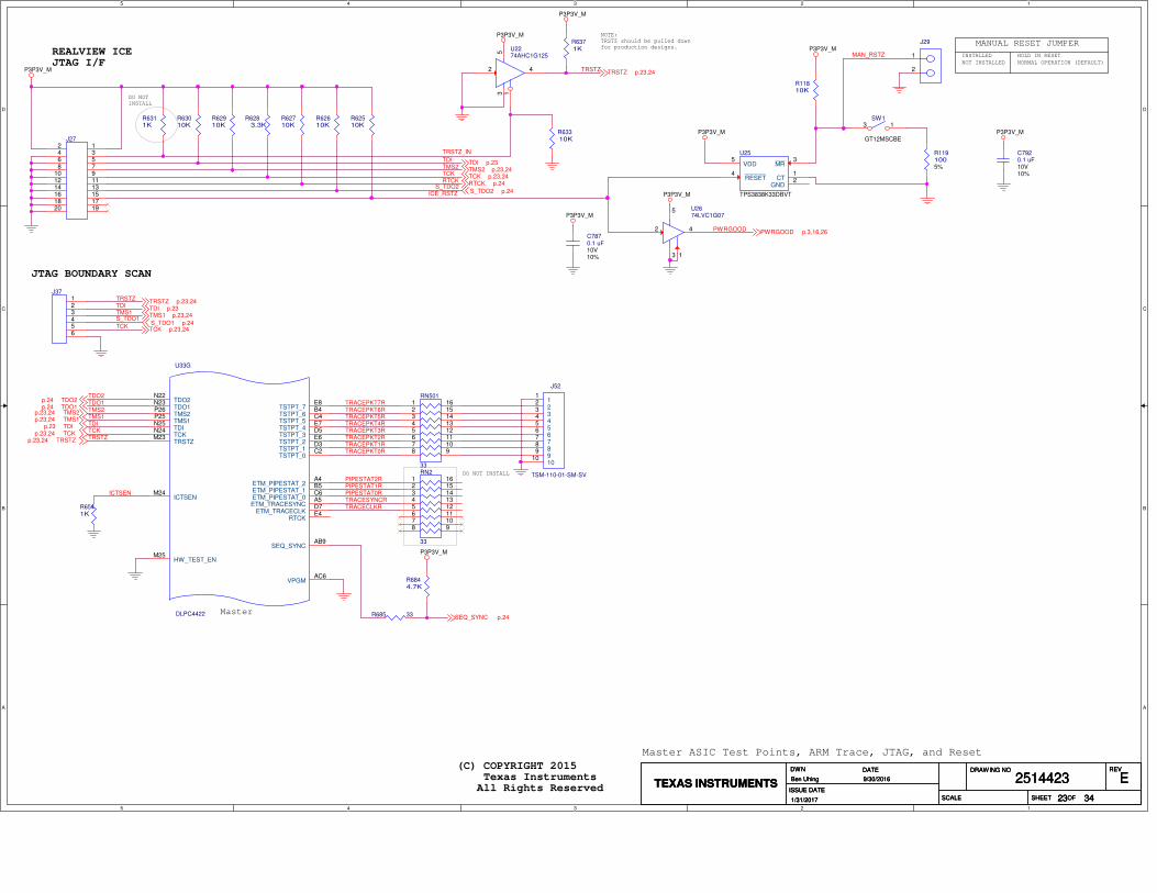
5
5
4
4
3
3
2
2
1
1
D D
C C
B B
A A
DO NOT INSTALL
JTAG BOUNDARY SCAN
DO NOT INSTALL
NOTE:TRSTZ should be pulled down for production designs.
REALVIEW ICEJTAG I/F
MANUAL RESET JUMPER
HOLD IN RESETINSTALLED
NOT INSTALLED NORMAL OPERATION (DEFAULT)
Master ASIC Test Points, ARM Trace, JTAG, and Reset
(C) COPYRIGHT 2015 Texas Instruments All Rights Reserved
Master
P3P3V_M
P3P3V_MP3P3V_M
P3P3V_M
P3P3V_M
P3P3V_M
P3P3V_M
P3P3V_M
P3P3V_M
TRSTZp.23,24TCKp.23,24TDIp.23TMS1p.23,24TMS2p.23,24
TDO1p.24TDO2p.24
S_TDO1 p.24
TRSTZ p.23,24TDI p.23
S_TDO2 p.24
TDI p.23
PWRGOOD p.3,16,26
TRSTZ p.23,24
TMS1 p.23,24
TCK p.23,24
TMS2 p.23,24TCK p.23,24RTCK p.24
SEQ_SYNC p.24
TEXAS INSTRUMENTS
DWN DATE
ISSUE DATE
SCALE
DRAWING NO REV
SHEET OF
2514423 E
3423
Ben Uhing 9/30/2016
1/31/2017
TEXAS INSTRUMENTS
DWN DATE
ISSUE DATE
SCALE
DRAWING NO REV
SHEET OF
2514423 E
3423
Ben Uhing 9/30/2016
1/31/2017
TEXAS INSTRUMENTS
DWN DATE
ISSUE DATE
SCALE
DRAWING NO REV
SHEET OF
2514423 E
3423
Ben Uhing 9/30/2016
1/31/2017
U25
TPS3838K33DBVT
CT1
MR3
GND2
VDD5
RESET4
R63310K
J29
1
2
R62510K
RN501
33
12345678 9
10111213141516
J52
TSM-110-01-SM-SV
11
22
33
44
55
66
77
88
99
1010
R11810K
R62910K
SW1
GT12MSCBE
3 1
C7920.1 uF10V10%
R6844.7K
R6371K
R1191005%
R6311K
J37123456
J271234567891011121314151617181920
R62710K
R685 33
R62610K
U2674LVC1G07
2 4
5
13
R6283.3K
C7870.1 uF10V10%
U33G
DLPC4422
TDO2N22
TDO1N23
TMS2P26
TMS1P25
TDIN25
TCKN24
TRSTZM23
ICTSENM24
HW_TEST_ENM25
TSTPT_0C2TSTPT_1D3TSTPT_2E6TSTPT_3D5TSTPT_4E7TSTPT_5C4TSTPT_6B4TSTPT_7E8
ETM_PIPESTAT_0C6ETM_PIPESTAT_1B5ETM_PIPESTAT_2A4
ETM_TRACESYNCA5
ETM_TRACECLKD7
RTCKE4
SEQ_SYNCAB9
VPGMAC6
R6541K
RN2
33
12345678 9
10111213141516
R63010K
U2274AHC1G125
2 4
513
TDO2TDO1TMS2TMS1TDITCKTRSTZ
ICTSEN
TRACEPKT1RTRACEPKT2RTRACEPKT3RTRACEPKT4RTRACEPKT5RTRACEPKT6RTRACEPKT7R
TRACEPKT0R
PIPESTAT2RPIPESTAT1RPIPESTAT0RTRACESYNCRTRACECLKR
TDITMS2
MAN_RSTZ
TRSTZ
TCKRTCK
S_TDO2ICE_RSTZ
PWRGOOD
TRSTZ
TRSTZ_IN
TDITMS1S_TDO1
TCK
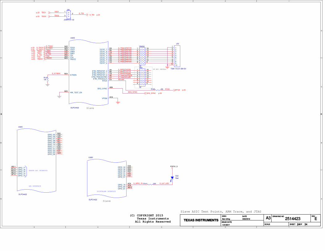
5
5
4
4
3
3
2
2
1
1
D D
C C
B B
A A
(C) COPYRIGHT 2015 Texas Instruments All Rights Reserved
Slave ASIC Test Points, ARM Trace, and JTAG
Slave
Slave
DO NOT INSTALL
P3P3V_S
TRSTZp.23TCKp.23S_TDIp.24TMS1p.23TMS2p.23
S_TDO1p.23S_TDO2p.23
RTCK p.23
SEQ_SYNC p.23
TDO1p.23
TDO2p.23S_TDI p.24
TEXAS INSTRUMENTS
DWN DATE
ISSUE DATE
SCALE
DRAWING NO REV
SHEET OF
2514423 EA3
3424
Ben Uhing 9/30/2016
1/31/2017
TEXAS INSTRUMENTS
DWN DATE
ISSUE DATE
SCALE
DRAWING NO REV
SHEET OF
2514423 EA3
3424
Ben Uhing 9/30/2016
1/31/2017
TEXAS INSTRUMENTS
DWN DATE
ISSUE DATE
SCALE
DRAWING NO REV
SHEET OF
2514423 EA3
3424
Ben Uhing 9/30/2016
1/31/2017
R141 220
J28
JUMPER-1x3
12
3
RN1
33
12345678 9
10111213141516
U32G
DLPC4422
TDO2N22
TDO1N23
TMS2P26
TMS1P25
TDIN25
TCKN24
TRSTZM23
ICTSENM24
HW_TEST_ENM25
TSTPT_0C2TSTPT_1D3TSTPT_2E6TSTPT_3D5TSTPT_4E7TSTPT_5C4TSTPT_6B4TSTPT_7E8
ETM_PIPESTAT_0C6ETM_PIPESTAT_1B5ETM_PIPESTAT_2A4
ETM_TRACESYNCA5
ETM_TRACECLKD7
RTCKE4
SEQ_SYNCAB9
VPGMAC6
POINTBLANK INTERFACE
U32D
DLPC4422
GPIO_30D25
GPIO_31F22
GPIO_32E24GPIO_33D26
GPIO_34F23
GPIO_57F25
GPIO_79AE9
GPIO_80AD9
GPIO_81AB10
J53
TSM-110-01-SM-SV
11
22
33
44
55
66
77
88
99
1010
R1271K
SENSOR ADC INTERFACE
LED INTERFACE
U32C
DLPC4422
GPIO_09B21
GPIO_10A22
GPIO_11A23
GPIO_21E20
GPIO_22D22
GPIO_23E21
GPIO_58G25
GPIO_73AF10 GPIO_74AE10 GPIO_75AD10 GPIO_76AC10 GPIO_77AB11
GPIO_05B20
GPIO_06C20
GPIO_07A20
GPIO_08A21
R160 33
D22
Red
RN500
33
12345678 9
10111213141516
S_TDO2S_TDO1
TMS2TMS1S_TDI
TCKTRSTZ
S_ICTSEN
S_TRACEPKT1RS_TRACEPKT2RS_TRACEPKT3RS_TRACEPKT4RS_TRACEPKT5RS_TRACEPKT6RS_TRACEPKT7R
S_TRACEPKT0R
S_PIPESTAT2RS_PIPESTAT1RS_PIPESTAT0RS_TRACESYNCRS_TRACECLKR
RTCKR
RTCK
SEQ_SYNC
TDO1
TDO2
S_TDI
S_GPIO_79 S_LLF_LED
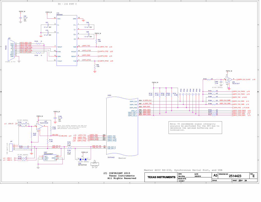
5
5
4
4
3
3
2
2
1
1
D D
C C
B B
A A
RS - 232 PORT 0
SOT-23
1 2
3
DO NOT INSTALL
Master ASIC RS-232, Synchronous Serial Port, and USB
(signal at PC)
USB type-B jack
Note: This buffer prevents the USB host from detecting the slave device before ARM processor initialization.
(C) COPYRIGHT 2015 Texas Instruments All Rights Reserved
Master
DO NOT INSTALL
Note: TI recommends signal intergrityanalysis be performed for the SPI bus todetermine the optimum buffering andtermination.
DO NOT INSTALL
DO NOT INSTALL
P3P3V_M
P3P3V_M
P3P3V_MP3P3V_M
P3P3V_M
P3P3V_M
P3P3V_M
P3P3V_M
SSP0_TXD_DMD p.14
UART0_CTSZ p.25
SSP0_TXD p.16,30
UART0_RXD p.25
SSP0_CSZ2_PMD1 p.16
SSP0_RXD p.14,16,30
SSP0_CSZ1_DMD p.14SSP0_CSZ0_DAD1 p.14
UART0_TXD p.25
UART0_RTSZ p.25
USB_ENZ p.21
SSP0_CLK_PMD1 p.16
SSP0_CLK_DMD p.14
SSP0_CSZ3_PMD2 p.16
UART0_CTSZp.25
UART0_TXDp.25
UART0_RTSZp.25
UART0_RXDp.25
SSP0_CLK_PMD2 p.16
SSP0_CLK_SLAVE p.30
USB+5Vp.3
USB_D-p.3
USB_D+p.3
TEXAS INSTRUMENTS
DWN DATE
ISSUE DATE
SCALE
DRAWING NO REV
SHEET OF
2514423 EA3
3425
Ben Uhing 9/30/2016
1/31/2017
TEXAS INSTRUMENTS
DWN DATE
ISSUE DATE
SCALE
DRAWING NO REV
SHEET OF
2514423 EA3
3425
Ben Uhing 9/30/2016
1/31/2017
TEXAS INSTRUMENTS
DWN DATE
ISSUE DATE
SCALE
DRAWING NO REV
SHEET OF
2514423 EA3
3425
Ben Uhing 9/30/2016
1/31/2017
R7253.3K
DN9BAT54CFILM
3
2 1
R9610K
R1623.3K
R159 22
TP
40
R15527.43/4W
R724 22
TP
45
J26
RS
23
2
DCD1
DSR6
RD2
RTS7
TD3
CTS8
DTR4
RING9
GND5
U3674LVC1G17
2 4
513
R161 22
U33H
DLPC4422
SSP0_CLKAD4
SSP0_TXDAB7
SSP0_RXDAD5
SSP0_CSZ_2AC3
SSP0_CSZ_1AB6
SSP0_CSZ_0AC5
UART0_TXDAB3
UART0_RXDAD1
UART0_CTSZAE2
UART0_RTSZAD2
USB_DAT_NC5
USB_DAT_PD6
GPIO_27AB4
R7173.3K
R166 22
R149 0
C590.1 uF10V10%
R718 22
C67
0.1 uF 50V
R158 0
J41
1234
TP
41
U16MAX3232
V+2
V-6
C1+1
C1-3
C2+4
C2-5
T1OUT14
T2OUT7
R1IN13
R2IN8
R2OUT9
R1OUT12
T1IN11
T2IN10
VCC16
GND15
R7223.3K
R165 22
U3774LVC1G125
2 4
513
C70
0.1 uF 50V
R154 0
TP
44
R146
27.43/4W
R721 22
R7193.3K
R163 0
TP
37
R1701.5K
R9710KR103 0
R168 22
C68
0.1 uF 50V
R147 0
TP
42
U507SN65220DBVT
NC11
GND12
NC33
A6
GND25
B4
R102 0
R7163.3K
R164 22
R16722K
TP
43
R726 22
C94012 pf
C1080.1 uF10V10%
C69
0.1 uF 50V
R152 0
USB_DAT_PS
USB_ENZ
UART0_TXD
UART0_CTSZ
UART0_RXD
UART0_RTSZ
UART0_RSTZ_CON
SSP0_CLK_DMDA_SSP0_CLK
SSP0_TXD_DMD
SSP0_RXD
SSP0_CSZ2SSP0_CSZ1SSP0_CSZ0
USB_DAT_P
UART0_DCD_CON
USB_DAT_NS
UART0_DSR_CONUART0_TXD_CONUART0_CTSZ_CONUART0_RXD_CON
UART0_DTR_CON
SSP0_CSZ3
A_SSP0_TXD
UART0_TXDUART0_RXDUART0_CTSZUART0_RTSZ
USB_DAT_N
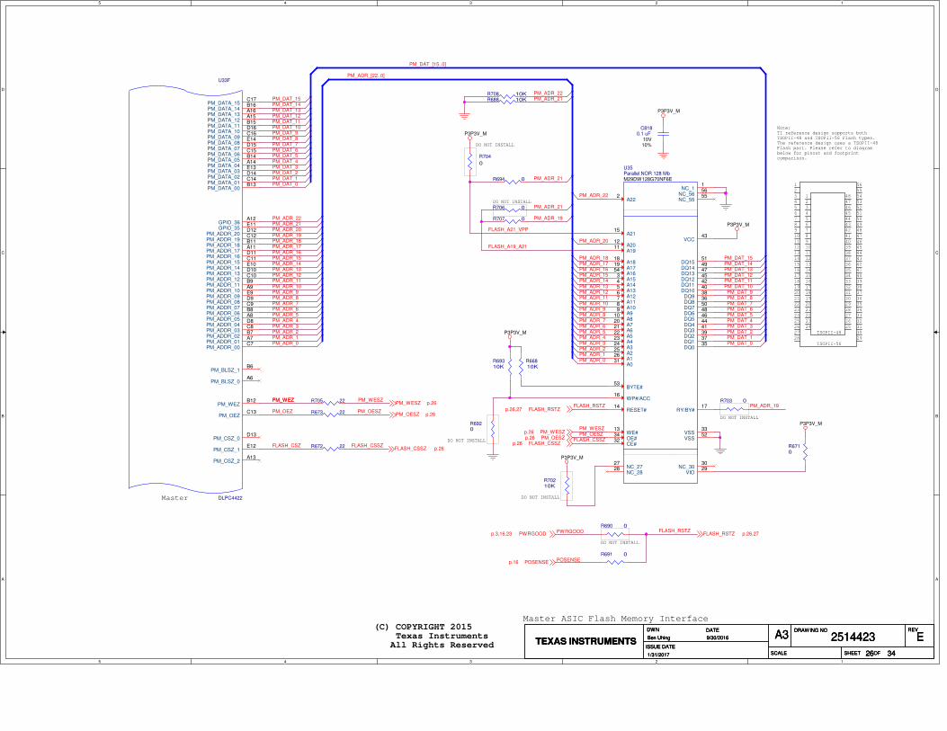
5
5
4
4
3
3
2
2
1
1
D D
C C
B B
A A
DO NOT INSTALL
DO NOT INSTALL
DO NOT INSTALL
DO NOT INSTALL
5
4
3
2
1
21
20
19
18
17
16
15
14
13
12
11
10
9
8
7
6
28
27
26
25
24
23
22
52
53
54
55
48
49
50
51
56
42
43
44
45
46
47
37
38
39
40
41
32
33
34
35
36
29
30
31
Note:TI reference design supports both TSOPII-48 and TSOPII-56 Flash types. The reference design uses a TSOPII-48Flash part. Please refer to diagram below for pinout and footprint comparison.
22
1
2
3
4
5
17
18
19
20
21
12
13
14
15
16
6
7
8
9
11
24
23
47
46
45
44
43
42
41
40
10
38
37
36
35
34
48
32
31
30
29
39
27
26
33
28
25
TSOPII-56
TSOPII-48
DO NOT INSTALL
DO NOT INSTALL
Master ASIC Flash Memory Interface (C) COPYRIGHT 2015 Texas Instruments All Rights Reserved
Master
P3P3V_M
P3P3V_M
P3P3V_M
P3P3V_M
P3P3V_M
P3P3V_M
PWRGOODp.3,16,23
PM_WESZ p.26
FLASH_RSTZ p.26,27
POSENSEp.16
PM_OESZ p.26FLASH_RSTZp.26,27
FLASH_CSSZ p.26FLASH_CSSZp.26
PM_OESZp.26PM_WESZp.26
TEXAS INSTRUMENTS
DWN DATE
ISSUE DATE
SCALE
DRAWING NO REV
SHEET OF
2514423 EA3
3426
Ben Uhing 9/30/2016
1/31/2017
TEXAS INSTRUMENTS
DWN DATE
ISSUE DATE
SCALE
DRAWING NO REV
SHEET OF
2514423 EA3
3426
Ben Uhing 9/30/2016
1/31/2017
TEXAS INSTRUMENTS
DWN DATE
ISSUE DATE
SCALE
DRAWING NO REV
SHEET OF
2514423 EA3
3426
Ben Uhing 9/30/2016
1/31/2017
R706 0
R6920
R70210K
R691 0
C8180.1 uF
10V10%
R673 22
R690 0
R705 22 R703 0
R688 10K
R6710
R708 10K
R69310K
R672 22
R66810K
R694 0
U33F
DLPC4422
PM_DATA_15C17
PM_DATA_14B16
PM_DATA_13A16
PM_DATA_12A15
PM_DATA_11B15
PM_DATA_10D16
PM_DATA_09C16
PM_DATA_08E14
PM_DATA_07D15
PM_DATA_06C15
PM_DATA_05B14
PM_DATA_04A14
PM_DATA_03E13
PM_DATA_02D14
PM_DATA_01C14
PM_DATA_00B13
GPIO_36A12
GPIO_35E11
PM_ADDR_20D12
PM_ADDR_19C12
PM_ADDR_18B11
PM_ADDR_17A11
PM_ADDR_16D11
PM_ADDR_15C11
PM_ADDR_14E10
PM_ADDR_13D10
PM_ADDR_12C10
PM_ADDR_11B9
PM_ADDR_10A9
PM_ADDR_09E9
PM_ADDR_08D9
PM_ADDR_07C9
PM_ADDR_06B8
PM_ADDR_05A8
PM_ADDR_04D8
PM_ADDR_03C8
PM_ADDR_02B7
PM_ADDR_01A7
PM_ADDR_00C7
PM_BLSZ_1B6
PM_BLSZ_0A6
PM_WEZB12
PM_OEZC13
PM_CSZ_0D13
PM_CSZ_1E12
PM_CSZ_2A13
U35Parallel NOR 128 MbM29DW128G70NF6E
DQ035DQ137DQ239DQ341DQ444DQ546DQ648DQ750DQ836DQ938DQ1040DQ1142DQ1245DQ1347DQ1449DQ1551
A031 A126 A225 A324 A423 A522 A621 A720 A810 A99 A108 A117 A126 A135 A144 A153 A16
54 A1719 A1818
A1911 A2012 VCC
43
VSS33
A2115
RESET#14
WE#13
OE#34
CE#32
WP#/ACC16
RY/BY#17
VSS52
BYTE#53
NC_5656
NC_5555
A222
NC_11
NC_2727
NC_2828
VIO29NC_3030
R704
0
R707 0
FLASH_CSZ
PM_ADR_0
PM_DAT_0
PM_OESZPM_ADR_19
PM_ADR_1PM_ADR_2PM_ADR_3PM_ADR_4PM_ADR_5PM_ADR_6PM_ADR_7PM_ADR_8PM_ADR_9PM_ADR_10PM_ADR_11PM_ADR_12PM_ADR_13PM_ADR_14
FLASH_RSTZ
PM_ADR_15PM_ADR_16PM_ADR_17PM_ADR_18PM_ADR_19PM_ADR_20PM_ADR_21PM_ADR_22
FLASH_A21_VPP
PM_ADR_21
PM_ADR_20
PM_WEZPM_WEZ
FLASH_CSSZ
PM_ADR_19
PM_DAT_1
PM_OEZ
PM_ADR_22PM_ADR_21
PM_ADR_[22..0]
PM_DAT_2PM_DAT_3PM_DAT_4PM_DAT_5PM_DAT_6PM_DAT_7
PM_WESZ
PM_DAT_[15..0]
PM_DAT_8PM_DAT_9PM_DAT_10PM_DAT_11PM_DAT_12PM_DAT_13PM_DAT_14
PWRGOOD
PM_DAT_15
PM_ADR_2PM_ADR_1
PM_ADR_7PM_ADR_6PM_ADR_5PM_ADR_4PM_ADR_3
PM_ADR_13PM_ADR_12PM_ADR_11PM_ADR_10PM_ADR_9PM_ADR_8
PM_ADR_18PM_ADR_17PM_ADR_16PM_ADR_15PM_ADR_14
PM_ADR_0
PM_DAT_15PM_DAT_14
PM_DAT_1PM_DAT_0
PM_DAT_6PM_DAT_5PM_DAT_4PM_DAT_3PM_DAT_2
PM_DAT_12PM_DAT_11PM_DAT_10
PM_DAT_9PM_DAT_8PM_DAT_7
PM_DAT_13
FLASH_A19_A21
PM_ADR_22
POSENSE
PM_OESZ
PM_ADR_21
PM_WESZ
FLASH_CSSZ
FLASH_RSTZ
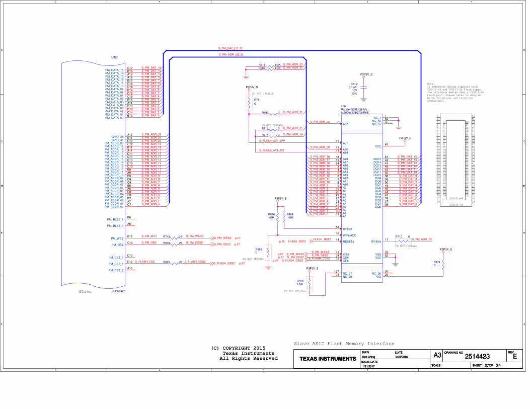
5
5
4
4
3
3
2
2
1
1
D D
C C
B B
A A
DO NOT INSTALL
DO NOT INSTALL
DO NOT INSTALL
5
4
3
2
1
21
20
19
18
17
16
15
14
13
12
11
10
9
8
7
6
28
27
26
25
24
23
22
52
53
54
55
48
49
50
51
56
42
43
44
45
46
47
37
38
39
40
41
32
33
34
35
36
29
30
31
Note:TI reference design supports both TSOPII-48 and TSOPII-56 Flash types. The reference design uses a TSOPII-48Flash part. Please refer to diagram below for pinout and footprint comparison.
22
1
2
3
4
5
17
18
19
20
21
12
13
14
15
16
6
7
8
9
11
24
23
47
46
45
44
43
42
41
40
10
38
37
36
35
34
48
32
31
30
29
39
27
26
33
28
25
TSOPII-56
TSOPII-48
DO NOT INSTALL
DO NOT INSTALL
(C) COPYRIGHT 2015 Texas Instruments All Rights Reserved
Slave ASIC Flash Memory Interface
Slave
P3P3V_S
P3P3V_S
P3P3V_S
P3P3V_S
P3P3V_S
P3P3V_S
S_PM_WESZ p.27
S_PM_OESZ p.27FLASH_RSTZp.26
S_FLASH_CSSZ p.27S_FLASH_CSSZp.27
S_PM_OESZp.27S_PM_WESZp.27
TEXAS INSTRUMENTS
DWN DATE
ISSUE DATE
SCALE
DRAWING NO REV
SHEET OF
2514423 EA3
3427
Ben Uhing 9/30/2016
1/31/2017
TEXAS INSTRUMENTS
DWN DATE
ISSUE DATE
SCALE
DRAWING NO REV
SHEET OF
2514423 EA3
3427
Ben Uhing 9/30/2016
1/31/2017
TEXAS INSTRUMENTS
DWN DATE
ISSUE DATE
SCALE
DRAWING NO REV
SHEET OF
2514423 EA3
3427
Ben Uhing 9/30/2016
1/31/2017
R69610K
R714 0
R676 22
R713 0
R675 22
R70910K
R712 22
C8190.1 uF
10V10%
R687 10K
R66910K
R697 0
U34Parallel NOR 128 MbM29DW128G70NF6E
DQ035DQ137DQ239DQ341DQ444DQ546DQ648DQ750DQ836DQ938DQ1040DQ1142DQ1245DQ1347DQ1449DQ1551
A031 A126 A225 A324 A423 A522 A621 A720 A810 A99 A108 A117 A126 A135 A144 A153 A16
54 A1719 A1818
A1911 A2012 VCC
43
VSS33
A2115
RESET#14
WE#13
OE#34
CE#32
WP#/ACC16
RY/BY#17
VSS52
BYTE#53
NC_5656
NC_5555
A222
NC_11
NC_2727
NC_2828
VIO29NC_3030
R6740
R711
0
R710 0
U32F
DLPC4422
PM_DATA_15C17
PM_DATA_14B16
PM_DATA_13A16
PM_DATA_12A15
PM_DATA_11B15
PM_DATA_10D16
PM_DATA_09C16
PM_DATA_08E14
PM_DATA_07D15
PM_DATA_06C15
PM_DATA_05B14
PM_DATA_04A14
PM_DATA_03E13
PM_DATA_02D14
PM_DATA_01C14
PM_DATA_00B13
GPIO_36A12
GPIO_35E11
PM_ADDR_20D12
PM_ADDR_19C12
PM_ADDR_18B11
PM_ADDR_17A11
PM_ADDR_16D11
PM_ADDR_15C11
PM_ADDR_14E10
PM_ADDR_13D10
PM_ADDR_12C10
PM_ADDR_11B9
PM_ADDR_10A9
PM_ADDR_09E9
PM_ADDR_08D9
PM_ADDR_07C9
PM_ADDR_06B8
PM_ADDR_05A8
PM_ADDR_04D8
PM_ADDR_03C8
PM_ADDR_02B7
PM_ADDR_01A7
PM_ADDR_00C7
PM_BLSZ_1B6
PM_BLSZ_0A6
PM_WEZB12
PM_OEZC13
PM_CSZ_0D13
PM_CSZ_1E12
PM_CSZ_2A13
R715 10K
R6950
S_FLASH_CSZ
S_PM_ADR_0
S_PM_DAT_0
S_PM_OESZS_PM_ADR_19
S_PM_ADR_1S_PM_ADR_2S_PM_ADR_3S_PM_ADR_4S_PM_ADR_5S_PM_ADR_6S_PM_ADR_7S_PM_ADR_8S_PM_ADR_9S_PM_ADR_10S_PM_ADR_11S_PM_ADR_12S_PM_ADR_13S_PM_ADR_14
FLASH_RSTZ
S_PM_ADR_15S_PM_ADR_16S_PM_ADR_17S_PM_ADR_18S_PM_ADR_19S_PM_ADR_20S_PM_ADR_21S_PM_ADR_22
S_FLASH_A21_VPP
S_PM_WESZ
S_PM_ADR_21
S_PM_ADR_20
S_PM_WEZ
S_FLASH_CSSZ
S_PM_ADR_19
S_PM_DAT_1
S_PM_OEZ
S_PM_ADR_22S_PM_ADR_21
S_PM_ADR_[22..0]
S_PM_DAT_2S_PM_DAT_3S_PM_DAT_4S_PM_DAT_5S_PM_DAT_6S_PM_DAT_7
S_PM_WESZ
S_PM_DAT_[15..0]
S_PM_DAT_8S_PM_DAT_9S_PM_DAT_10S_PM_DAT_11S_PM_DAT_12S_PM_DAT_13S_PM_DAT_14S_PM_DAT_15
S_PM_ADR_2S_PM_ADR_1
S_PM_ADR_7S_PM_ADR_6S_PM_ADR_5S_PM_ADR_4S_PM_ADR_3
S_PM_ADR_13S_PM_ADR_12S_PM_ADR_11S_PM_ADR_10S_PM_ADR_9S_PM_ADR_8
S_PM_ADR_18S_PM_ADR_17S_PM_ADR_16S_PM_ADR_15S_PM_ADR_14
S_PM_ADR_0
S_PM_DAT_15S_PM_DAT_14
S_PM_DAT_1S_PM_DAT_0
S_PM_DAT_6S_PM_DAT_5S_PM_DAT_4S_PM_DAT_3S_PM_DAT_2
S_PM_DAT_12S_PM_DAT_11S_PM_DAT_10
S_PM_DAT_9S_PM_DAT_8S_PM_DAT_7
S_PM_DAT_13
S_FLASH_A19_A21
S_PM_ADR_22
S_PM_OESZ
S_PM_ADR_21
S_FLASH_CSSZ

5
5
4
4
3
3
2
2
1
1
D D
C C
B B
A A
ADC INTEGRATING SENSOR BOARD I/F
LIGHT TO FREQUENCY SENSOR I/F
Master ASIC SSI Sensor Interface (C) COPYRIGHT 2015 Texas Instruments All Rights Reserved
Master
P5V_M
P3P3V_MP3P3V_M
P5V_M
LED6_PWM p.29LED7_PWM p.29
GPIO_21 p.29SUBFRAME p.29GPIO_23 p.29SENSE_PULSE p.29
LED8_PWM p.29
GRN_PWM p.29BLU_PWM p.29LED4_PWM p.29LED5_PWM p.29
TEXAS INSTRUMENTS
DWN DATE
ISSUE DATE
SCALE
DRAWING NO REV
SHEET OF
2514423 EA3
3428
Ben Uhing 9/30/2016
1/31/2017
TEXAS INSTRUMENTS
DWN DATE
ISSUE DATE
SCALE
DRAWING NO REV
SHEET OF
2514423 EA3
3428
Ben Uhing 9/30/2016
1/31/2017
TEXAS INSTRUMENTS
DWN DATE
ISSUE DATE
SCALE
DRAWING NO REV
SHEET OF
2514423 EA3
3428
Ben Uhing 9/30/2016
1/31/2017
R140 33
TP
53
J38
JUMPER-1x3
12
3
C9590.1 uF
10V10%
R679 33
SENSOR ADC INTERFACE
LED INTERFACE
U33C
DLPC4422
GPIO_09B21
GPIO_10A22
GPIO_11A23
GPIO_21E20
GPIO_22D22
GPIO_23E21
GPIO_58G25
GPIO_73AF10 GPIO_74AE10 GPIO_75AD10 GPIO_76AC10 GPIO_77AB11
GPIO_05B20
GPIO_06C20
GPIO_07A20
GPIO_08A21
C9600.1 uF
10V10%
R682 33
TP
48
TP
54
R680 33
TP
49
TP
55
J45
12 HEADER
123456789101112
J48
CON3
123
LED6_PWM
LED8_PWM
SUBFRAME
SENSE_PULSEGPIO_23
ADC_CSZ
ADC_SDO
ADC_SCLK
ADC_RST
ADC_SDIN
LED7_PWM
GPIO_21
FREQ_SENSOR
ADC_SDO
FREQ_SENSOR
ADC_RSTADC_CSZGPIO_75ADC_SDINADC_SCLK
LED5_PWMLED4_PWMBLU_PWMGRN_PWM
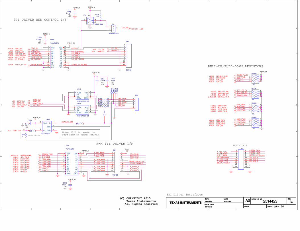
5
5
4
4
3
3
2
2
1
1
D D
C C
B B
A A
SPI DRIVER AND CONTROL I/F
PWM SSI DRIVER I/F
PULL-UP/PULL-DOWN RESISTORS
TESTPOINTS
SSI Driver Interfaces
(C) COPYRIGHT 2015 Texas Instruments All Rights Reserved
DO NOT INSTALL
Note: U529 is needed to read from an OSRAM driver
P3P3V_M
P3P3V_M
P3P3V_M
P3P3V_M
P3P3V_M
P12V
P3P3V_M
P3P3V_M
P3P3V_M
P3P3V_M
DB/RED_PWMp.20,21,29GRN_PWMp.28,29BLU_PWMp.28,29LED4_PWMp.28,29LED5_PWMp.28,29LED6_PWMp.28,29LED7_PWMp.28,29LED8_PWMp.28,29GPIO_21p.28,29GPIO_23p.28,29
SSP2_DOp.21SSP2_CLKp.21
SSP2_CSZ_0p.21DRV_RSTp.21
GPIO_54p.21,29LMPCTRLp.21SUBFRAMEp.28,29RED_LED_ENp.21,29GRN_LED_ENp.21,29BLU_LED_ENp.21,293D_TOGGLEp.20,21
SENSE_PULSEp.28,29
LAMPLITZp.21
DB/RED_PWMp.20,21,29
GRN_PWMp.28,29BLU_PWMp.28,29LED4_PWMp.28,29LED5_PWMp.28,29
LED6_PWMp.28,29LED7_PWMp.28,29LED8_PWMp.28,29
SENSE_PULSEp.28,29SUBFRAMEp.28,29GPIO_21p.28,29GPIO_23p.28,29
GRN_LED_ENp.21,29BLU_LED_ENp.21,29
RED_LED_ENp.21,29
LED_EN p.29
LED_ENp.29
GPIO_54p.21,29
SSP2_DINp.21
TEXAS INSTRUMENTS
DWN DATE
ISSUE DATE
SCALE
DRAWING NO REV
SHEET OF
2514423 EA3
3429
Ben Uhing 9/30/2016
1/31/2017
TEXAS INSTRUMENTS
DWN DATE
ISSUE DATE
SCALE
DRAWING NO REV
SHEET OF
2514423 EA3
3429
Ben Uhing 9/30/2016
1/31/2017
TEXAS INSTRUMENTS
DWN DATE
ISSUE DATE
SCALE
DRAWING NO REV
SHEET OF
2514423 EA3
3429
Ben Uhing 9/30/2016
1/31/2017
J36
CON22
1 23 45 67 89 10
11 1213 1415 1617 1819 2021 22
U39
74LVC827A
Y123
Y222
Y321
Y420
Y519
Y618
Y717
Y816
A12
A23
A34
A45
A56
A67
A78
A89
GND12
OE11
A910
A1011 Y9
15
Y1014
OE213
VCC24
C9560.1 uF
10V10%
U511
SN74LVC2G125
1OEz1
1A2
2Y3
GND42A
5 1Y6
2OEz7
Vcc8
J39
CON12
123456789
101112
R736 33
RN503
10K
1234
765
8
R734 0
U512
SN74LVC2G125
1OEz1
1A2
2Y3
GND42A
5 1Y6
2OEz7
Vcc8
R13610K
TP
46
R739 0
J34
JUMPER-1x3
12
3
RN505
10K
1234
765
8
C9640.1 uF10V10%
C9630.1 uF10V10%
TP
50
R7400
C9440.1 uF
10V10%
RN504
10K
1234
765
8
RN502
10K
1234
765
8
TP
51
R738 33
TP
52
U30
74LVC1G06
1
3
4
5
2
R744 33T
P4
7
U508
74LVC827A
Y123
Y222
Y321
Y420
Y519
Y618
Y717
Y816
A12
A23
A34
A45
A56
A67
A78
A89
GND12
OE11
A910
A1011 Y9
15
Y1014
OE213
VCC24
J49
123456
C965
0.1 uF10V10%
C1160.1 uF
10V10%
R735 33
R737 33
U513
74AUP1G79
D1
CLK2
GND3
Q4
VCC5
J441 23 45 67 89 10
11 1213 1415 1617 1819 20
LED_SCLK
SSP2_DOSSP2_CLK
DB/RED_PWMGRN_PWMBLU_PWMLED4_PWMLED5_PWMLED6_PWMLED7_PWMLED8_PWMGPIO_21GPIO_23
LED_DIN
SSP2_CSZ_0DRV_RST
SSI_SUBFRAMESSI_STB_RSSI_STB_GSSI_STB_B
A_SPARE_1GPIO_54
LMPCTRLSUBFRAMERED_LED_ENGRN_LED_ENBLUE_LED_EN3D_TOGGLE
SENSE_PULSE
A_RED_PWMA_GRN_PWMA_BLU_PWM
A_LED4_PWMA_LED5_PWMA_LED6_PWM
A_LED7_PWMA_LED8_PWM
LAMPLITZ
LED_EN
LED_EN
DB/RED_PWM
GRN_PWMBLU_PWMLED4_PWMLED5_PWM
LED6_PWMLED7_PWMLED8_PWM
SUBFRAMEGPIO_21GPIO_23
GRN_LED_ENBLU_LED_EN
RED_LED_EN
SENSE_PULSE
SENSE_PULSE_BUF
SSI_3D_TOGGLE
LED_DIR
A_RED_PWMA_GRN_PWMA_BLU_PWMSSI_SUBFRAMEA_LED7_PWMA_LED8_PWMSSI_3D_TOGGLE
A_LED4_PWMA_LED5_PWMA_LED6_PWMSENSE_PULSE_BUFSSI_STB_RSSI_STB_GSSI_STB_B
A_SPARE_2A_SPARE_3A_SPARE_1
SSI_SUBFRAME
SENSE_PULSE_BUFSSI_3D_TOGGLE
SSI_STB_RSSI_STB_GSSI_STB_B
GPIO_54
SSP2/LED_DIN
LED_OELED_DOUT
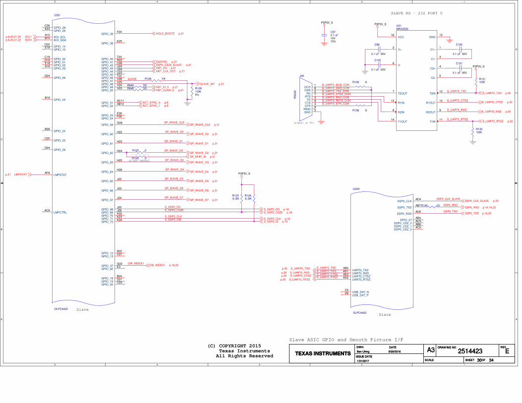
5
5
4
4
3
3
2
2
1
1
D D
C C
B B
A A
(C) COPYRIGHT 2015 Texas Instruments All Rights Reserved
Slave ASIC GPIO and Smooth Picture I/F
Slave
Slave
DO NOT INSTALL
SLAVE RS - 232 PORT 0
(signal at PC)
P3P3V_S
P3P3V_SP3P3V_S
P3P3V_S
HBT_CLKIN_0 p.21HBT_DI_0 p.21
SSP0_CSZ4_SLAVE p.21DASYNC p.21
SLAVE_INT p.21
SCL1p.8,20,21,22SDA1p.8,20,21,22
LMPSTATp.21
HBT_CLK_OUT p.21HBT_DO p.21
HOLD_BOOTZ p.21
SP_WAVE_CLK p.31
SP_WAVE_D0 p.31
SP_WAVE_D1 p.31
SP_WAVE_D2 p.31
SP_WAVE_D3 p.31
SP_WAVE_D4 p.31
SP_WAVE_D5 p.31
SP_WAVE_D6 p.31
SP_WAVE_D7 p.31 SSP0_CLK_SLAVE p.25
SSP0_TXD p.16,25
SSP0_RXD p.14,16,25
SP_STAT_IN p.31
S_SSP2_DO p.16S_SSP2_CSZ0 p.16
S_SSP2_CLK p.16S_SSP2_DI p.16
S_UART0_CTSZ p.30
S_UART0_RXD p.30
S_UART0_TXD p.30
S_UART0_RTSZ p.30
S_UART0_CTSZp.30
S_UART0_TXDp.30
S_UART0_RTSZp.30
S_UART0_RXDp.30
ACT_SYNC_0 p.8ACT_SYNC_1 p.8
CW_INDEX1 p.16,20
TEXAS INSTRUMENTS
DWN DATE
ISSUE DATE
SCALE
DRAWING NO REV
SHEET OF
2514423 EA3
3430
Ben Uhing 9/30/2016
1/31/2017
TEXAS INSTRUMENTS
DWN DATE
ISSUE DATE
SCALE
DRAWING NO REV
SHEET OF
2514423 EA3
3430
Ben Uhing 9/30/2016
1/31/2017
TEXAS INSTRUMENTS
DWN DATE
ISSUE DATE
SCALE
DRAWING NO REV
SHEET OF
2514423 EA3
3430
Ben Uhing 9/30/2016
1/31/2017
U32H
DLPC4422
SSP0_CLKAD4
SSP0_TXDAB7
SSP0_RXDAD5
SSP0_CSZ_2AC3
SSP0_CSZ_1AB6
SSP0_CSZ_0AC5
UART0_TXDAB3
UART0_RXDAD1
UART0_CTSZAE2
UART0_RTSZAD2
USB_DAT_NC5
USB_DAT_PD6
GPIO_27AB4
C102
0.1 uF 50V
R649 33
C99
0.1 uF 50V
J35
RS
23
2
DCD1
DSR6
RD2
RTS7
TD3
CTS8
DTR4
RING9
GND5
R648 33
R13110K
C100
0.1 uF 50V
C101
0.1 uF 50V
R138 0
U32I
DLPC4422
GPIO_28C26
GPIO_29E23
IIC0_SCLA10
IIC0_SDAB10
GPIO_00C19
GPIO_01D19
GPIO_02E18
GPIO_03A19
GPIO_14D20
GPIO_15E19
GPIO_39F24
GPIO_38E25
GPIO_37G22
GPIO_18B24
GPIO_19D21
GPIO_20C23
GPIO_12B22
GPIO_13C21
GPIO_24B26
GPIO_25C25
GPIO_26D24
LMPSTATAF8
LMPCTRLAC9
GPIO_40T23
GPIO_41R22
GPIO_42U26
GPIO_43U25
GPIO_44U24
GPIO_45U23
GPIO_46T22
GPIO_47V26
GPIO_48V25
GPIO_49V24
GPIO_50V23
GPIO_51AC11
GPIO_52AB12
GPIO_53E26
GPIO_54F26
GPIO_56G24
GPIO_59G26
GPIO_60H22
GPIO_61H23
GPIO_62H24
GPIO_63H25
GPIO_64H26
GPIO_65J22
GPIO_66J23
GPIO_67J24
GPIO_68J25
GPIO_69J26
GPIO_70K22
GPIO_71K23
GPIO_72K24
GPIO_82E3
GPIO_04B19
R1253.3K
C970.1 uF10V10%
R145 22
R123 0
U31MAX3232
V+2
V-6
C1+1
C1-3
C2+4
C2-5
T1OUT14
T2OUT7
R1IN13
R2IN8
R2OUT9
R1OUT12
T1IN11
T2IN10
VCC16
GND15
R1263.3K
R12910K5%
R139 0
R128 1K
R124 0
R13010K
SLAVE
SP_WAVE_D5
SP_WAVE_D3
SP_WAVE_CLK
SP_WAVE_D0
SP_WAVE_D1
SP_WAVE_D4
SP_WAVE_D6
SP_WAVE_D7 SSP0_CLK_SLAVE
SSP0_RXD
SSP0_TXD
SP_WAVE_D2
S_SSP2_DOS_SSP2_CSZ0
S_SSP2_CLKS_SSP2_DIN
S_UART0_TXD
S_UART0_CTSZ
S_UART0_RXD
S_UART0_RTSZ
S_UART0_RSTZ_CON
S_UART0_DCD_CONS_UART0_DSR_CONS_UART0_TXD_CONS_UART0_CTSZ_CONS_UART0_RXD_CON
S_UART0_DTR_CON
S_UART0_TXDS_UART0_RXDS_UART0_CTSZS_UART0_RTSZ
CW_INDEX1
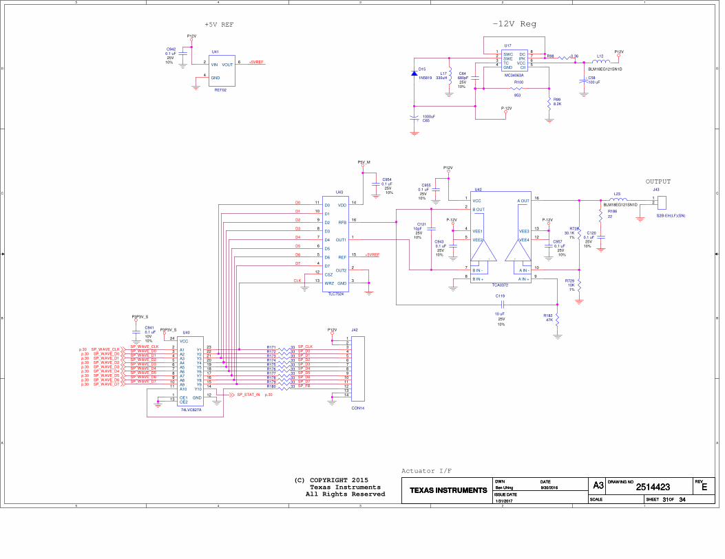
5
5
4
4
3
3
2
2
1
1
D D
C C
B B
A A
OUTPUT
+5V REF -12V Reg
Actuator I/F
(C) COPYRIGHT 2015 Texas Instruments All Rights Reserved
P12VP3P3V_S
P3P3V_S
P5V_M
P-12V P-12V
P12V
P12V
P-12V
P12V
SP_STAT_IN p.30
SP_WAVE_CLKp.30SP_WAVE_D0p.30SP_WAVE_D1p.30SP_WAVE_D2p.30SP_WAVE_D3p.30SP_WAVE_D4p.30SP_WAVE_D5p.30SP_WAVE_D6p.30SP_WAVE_D7p.30
TEXAS INSTRUMENTS
DWN DATE
ISSUE DATE
SCALE
DRAWING NO REV
SHEET OF
2514423 EA3
3431
Ben Uhing 9/30/2016
1/31/2017
TEXAS INSTRUMENTS
DWN DATE
ISSUE DATE
SCALE
DRAWING NO REV
SHEET OF
2514423 EA3
3431
Ben Uhing 9/30/2016
1/31/2017
TEXAS INSTRUMENTS
DWN DATE
ISSUE DATE
SCALE
DRAWING NO REV
SHEET OF
2514423 EA3
3431
Ben Uhing 9/30/2016
1/31/2017
J42
CON14
123456789
1011121314
R998.2K
R72830.1K
1%
R100
953
R171 33
C119
10 uF
25V
10%
U40
74LVC827A
A12
A23
A34
A45
A56
A67
A78
A89
A910
A1011
Y1014Y915Y816Y717Y618Y519Y420Y321Y222Y123
VCC24
GND12
OE11
OE213
R172 33
C9430.1 uF25V
10%
R173 33
U43
TLC7524
D74
D65
D56
D47
D38
WRZ13
CSZ12
D29
D110
D011
VDD14
REF15
GND3
OUT11
OUT22
RFB16
C9410.1 uF10V10%
D15
1N5819
J43
S2B-EH(LF)(SN)
12
+ -+-
U42
TCA0372
A IN -10
A IN +9
B OUT2
VEE14
VEE25
B IN -7
A OUT16
VEE313
VEE412
VCC1
B IN +8
U41
REF02
VIN2
GND4
VOUT6
R174 33
R98 0.36
R18247K
C9420.1 uF25V
10%
C1200.1 uF25V
10%
R175 33R176 33
C12110pF
25V10%
U17
MC34063A
SWC1
SWE2
TC3
GND4
CII5VCC6IPK7DC8
R178 33
L17330uH
C9550.1 uF25V
10%
R177 33
L12
BLM18EG121SN1D
L23
BLM18EG121SN1D
R186
22
C9570.1 uF
25V10%
+ C58100 uF
R180 33R179 33
+
C651000uF
R72910K1%
C64680pF25V
10%
C9540.1 uF
25V10%
SP_D3
SP_D1SP_D0SP_CLK
SP_D5SP_D6SP_D7SP_FB
SP_D2
SP_D4
SP_WAVE_CLKSP_WAVE_D0SP_WAVE_D1SP_WAVE_D2SP_WAVE_D3SP_WAVE_D4SP_WAVE_D5SP_WAVE_D6SP_WAVE_D7
D0
D1
D2
D7
D6
D5
D4
D3
CLK
+5VREF
+5VREF

5
5
4
4
3
3
2
2
1
1
D D
C C
B B
A A
DLPC4422 P1P1V Bypass Capacitors
DLPC4422 P1P8V DRAM Bypass Capacitors
DLPC4422 P3P3V Bypass Capacitors
DLPC4422 P1P8V LVDS Bypass Capacitors
Master DLPC4422 Power and Bypass Capacitors
(C) COPYRIGHT 2015 Texas Instruments All Rights Reserved
Master
P1P1V_M
P1P8V_M
P1P8V_M
P3P3V_M
P1P1V_M
P1P8V_M
P3P3V_M P1P8V_M P1P8V_M
P1P1V_M PLLM1_VDD
PLLM2_VDD
PLLD_VDDPLLD_VAD
A1P8V_M PLLM1_VAD
PLLM2_VAD
PLLS_VAD
PLLD_VAD
PLLM2_VAD
P3P3V_M
PLLS_VAD
P1P1V_MPLLM1_VDD
PLLM1_VAD
PLLM2_VDD
PLLD_VDD
TEXAS INSTRUMENTS
DWN DATE
ISSUE DATE
SCALE
DRAWING NO REV
SHEET OF
2514423 EA3
3432
Ben Uhing 9/30/2016
1/31/2017
TEXAS INSTRUMENTS
DWN DATE
ISSUE DATE
SCALE
DRAWING NO REV
SHEET OF
2514423 EA3
3432
Ben Uhing 9/30/2016
1/31/2017
TEXAS INSTRUMENTS
DWN DATE
ISSUE DATE
SCALE
DRAWING NO REV
SHEET OF
2514423 EA3
3432
Ben Uhing 9/30/2016
1/31/2017
C8060.1 uF10V10%
C9360.1 uF10V10%
C8200.1 uF10V10%
R640 1.00
C9020.1 uF10V10%
C8590.1 uF10V10%
C9210.1 uF10V10%
C8270.1 uF10V10%
C9090.1 uF10V10%
C8260.1 uF10V10%
C817100 uF6.3V20%
C9180.1 uF10V10%
C8250.1 uF10V10%
C8220.1 uF10V10%
C9160.1 uF10V10%
C9060.1 uF10V10%
C9040.1 uF10V10%
C8400.1 uF10V10%
FB506 470 Ohm
BLM18AG471SN1D
C9370.1 uF10V10%
FB504 470 Ohm
BLM18AG471SN1D
C8670.1 uF10V10%
C10310 uF10V10%
C8470.1 uF10V10%
C8000.1 uF10V10%
C9070.1 uF10V10%
C8020.1 uF10V10%
C8420.1 uF10V10%
C8620.1 uF10V10%
C9330.1 uF10V10%
C9100.1 uF10V10%
C8370.1 uF10V10%
C8850.1 uF10V10%
C8390.1 uF10V10%
C8280.1 uF10V10%
FB507 470 Ohm
BLM18AG471SN1D
C8630.1 uF10V10%
FB505 470 Ohm
BLM18AG471SN1D
R639 0.36
C8890.1 uF10V10%
C87310 uF10V10%
C89210 uF10V10%
C9080.1 uF10V10%
C8760.1 uF10V10%
C7910.1 uF10V10%
C8240.1 uF10V10%
C9170.1 uF10V10%
C85310 uF10V10%
C8040.1 uF10V10%
C7900.1 uF10V10%
C9200.1 uF10V10%
C91100 uF
C8030.1 uF10V10%
C8860.1 uF10V10%
C8560.1 uF10V10%
C8550.1 uF10V10%
C940.1 uF10V10%
C8230.1 uF10V10%
C8810.1 uF10V10%
C8900.1 uF10V10%
C9340.1 uF10V10%
FB3 470 Ohm
BLM18AG471SN1D
C9150.1 uF10V10%
C9190.1 uF10V10%
C8820.1 uF10V10%
C8520.1 uF10V10%
C9050.1 uF10V10%
C87210 uF10V10%
C9610 uF10V10%
FB509 470 Ohm
BLM18AG471SN1D
C8950.1 uF10V10%
C851100 uF6.3V20%
FB508 470 Ohm
BLM18AG471SN1D
U33J
DLPC4422DLPC4422
GN
D_A
1A
1
GN
D_A
2A
2
GN
D_A
3A
3
GN
D_A
24
A24
GN
D_A
25
A25
GN
D_A
26
A26
GN
D_B
1B
1
GN
D_B
2B
2
GN
D_B
3B
3
GN
D_B
25
B25
GN
D_C
3C
3
GN
D_C
24
C24
GN
D_D
4D
4
GN
D_D
23
D23
GN
D_E
5E
5
GN
D_E
22
E22
GN
D_F
6F
6
GN
D_F
9F
9
GN
D_F
12
F12
GN
D_F
15
F15
GN
D_F
18
F18
GN
D_F
21
F21
GN
D_G
5G
5
GN
D_J5
J5
GN
D_J6
J6
GN
D_J21
J21
GN
D_L5
L5
GN
D_N
5N
5
GN
D_R
6R
6
VD
DC
_T
21
T21
VD
DC
_T
16
T16
VD
DC
_T
11
T11
VD
DC
_P
6P
6V
DD
C_N
21
N21
VD
DC
_L16
L16
GN
D_L12
L12
GN
D_L13
L13
GN
D_L14
L14
GN
D_L15
L15
GN
D_M
6M
6
GN
D_M
21
M21
GN
D_M
11
M11
GN
D_M
12
M12
GN
D_M
13
M13
GN
D_M
14
M14
GN
D_M
15
M15
GN
D_M
16
M16
GN
D_N
11
N11
GN
D_N
12
N12
GN
D_N
13
N13
GN
D_N
14
N14
GN
D_N
15
N15
GN
D_N
16
N16
GN
D_P
11
P11
GN
D_P
12
P12
GN
D_P
13
P13
GN
D_P
14
P14
GN
D_P
15
P15
GN
D_P
16
P16
GN
D_R
5R
5
GN
D_R
11
R11
GN
D_R
12
R12
GN
D_R
13
R13
GN
D_R
14
R14
GN
D_R
15
R15
GN
D_R
16
R16
GN
D_U
5U
5
GN
D_V
6V
6
GN
D_V
21
V21
GN
D_T
12
T12
GN
D_T
13
T13
GN
D_T
14
T14
GN
D_T
15
T15
GN
D_W
5W
5
GN
D_Y
5Y
5
GN
D_A
A6
AA
6
GN
D_A
A9
AA
9
GN
D_A
A12
AA
12
GN
D_A
A15
AA
15
GN
D_A
A18
AA
18
GN
D_A
A21
AA
21
GN
D_A
B5
AB
5
GN
D_A
B22
AB
22
GN
D_A
C4
AC
4
GN
D_A
C23
AC
23
GN
D_A
D3
AD
3
GN
D_A
D24
AD
24
GN
D_A
E3
AE
3
GN
D_A
E24
AE
24
GN
D_A
E25
AE
25
GN
D_A
F1
AF
1
GN
D_A
F3
AF
3G
ND
_A
F2
AF
2
GN
D_A
F24
AF
24
GN
D_A
F25
AF
25
GN
D_A
F26
AF
26
PLLD
_V
SS
L23
PLLD
_V
DD
L22
PLLD
_V
AS
K26
PLLD
_V
AD
K25
PLLM
1_V
SS
M22
VD
DC
_F
7F
7
VD
DC
_F
10
F10
VD
DC
_F
13
F13
VD
DC
_F
16
F16
VD
DC
_F
19
F19
VD
DC
_G
21
G21
VD
DC
_H
6H
6
VD
DC
_K
21
K21
VD
DC
_L6
L6
VD
DC
_L11
L11
DR
AM
VD
D_F
14
F14
DR
AM
VD
D_H
5H
5
DR
AM
VD
D_H
21
H21
DR
AM
VD
D_N
6N
6
DR
AM
VD
D_P
21
P21
DR
AM
VD
D_T
6T
6
DR
AM
VD
D_U
21
U21
DR
AM
VD
D_A
A13
AA
13
LV
DS
AV
D_C
1C
1
LV
DS
AV
D_F
5F
5
VD
DC
_A
A14
AA
14
VD
DC
_A
A17
AA
17
VD
DC
_A
A20
AA
20
VD
DC
_U
6U
6
VD
DC
_W
21
W21
VD
DC
_Y
6Y
6
VD
DC
_A
A8
AA
8
VD
DC
_A
A11
AA
11
VD
D33_F
8F
8
VD
D33_F
11
F11
VD
D33_F
17
F17
VD
D33_F
20
F20
VD
D33_L21
L21
VD
D33_R
21
R21
VD
D33_Y
21
Y21
VD
D33_A
A7
AA
7
VD
D33_A
A10
AA
10
VD
D33_A
A16
AA
16
VD
D33_A
A19
AA
19
PLLM
2_V
AD
R25
LV
DS
_A
VS
1K
5
LV
DS
_A
VS
2V
5
PLLS
_V
AD
R23
PLLS
_V
AS
R24
PLLM
1_V
AD
L24
PLLM
2_V
AS
R26
PLLM
1_V
AS
L25
LV
DS
AV
D_A
E1
AE
1
PLLM
2_V
DD
P23
PLLM
1_V
DD
L26
PLLM
2_V
SS
P24
LV
DS
AV
D_G
6G
6
LV
DS
AV
D_K
6K
6
LV
DS
AV
D_M
5M
5
LV
DS
AV
D_P
5P
5
LV
DS
AV
D_T
5T
5
LV
DS
AV
D_W
6W
6
LV
DS
AV
D_A
A5
AA
5
L_V
DQ
PA
D_0
D17
L_V
DQ
PA
D_1
A17
L_V
DQ
PA
D_2
C18
L_V
DQ
PA
D_3
A18
L_V
DQ
PA
D_4
E17
L_V
DQ
PA
D_5
B17
L_V
DQ
PA
D_6
D18
L_V
DQ
PA
D_7
B18
R_V
DQ
PA
D_0
AD
18
R_V
DQ
PA
D_1
AB
17
R_V
DQ
PA
D_2
AD
17
R_V
DQ
PA
D_3
AB
16
R_V
DQ
PA
D_4
AC
18
R_V
DQ
PA
D_5
AF
17
R_V
DQ
PA
D_6
AC
17
R_V
DQ
PA
D_7
AE
17
VT
ES
T1
AB
14
VT
ES
T2
AB
15
VT
ES
T3
E15
VT
ES
T4
E16
CF
O_V
DD
33
AE
26
C8960.1 uF10V10%
C11210 uF10V10%
C8410.1 uF10V10%
C9010.1 uF10V10%
C8770.1 uF10V10%
C8680.1 uF10V10%
C8050.1 uF10V10%
C8600.1 uF10V10%
C90100 uF
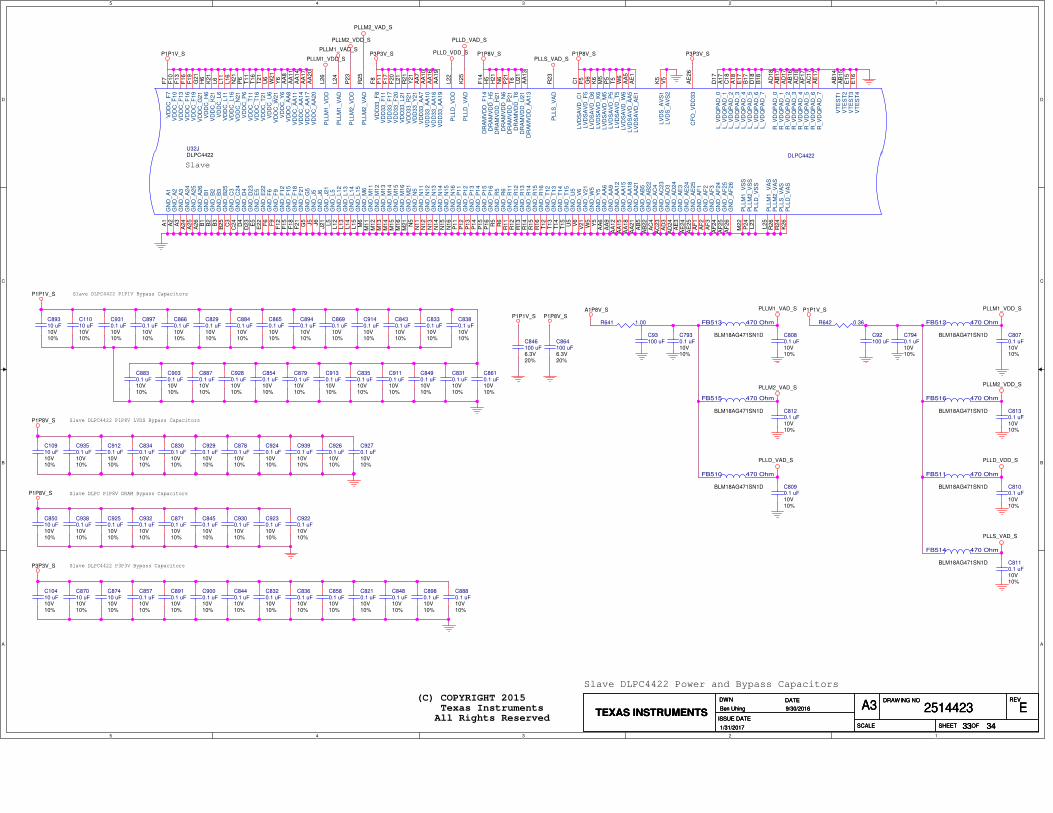
5
5
4
4
3
3
2
2
1
1
D D
C C
B B
A A
Slave DLPC4422 P1P1V Bypass Capacitors
Slave DLPC P1P8V DRAM Bypass Capacitors
Slave DLPC4422 P3P3V Bypass Capacitors
Slave DLPC4422 P1P8V LVDS Bypass Capacitors
Slave DLPC4422 Power and Bypass Capacitors
(C) COPYRIGHT 2015 Texas Instruments All Rights Reserved
Slave
P1P1V_S
P1P8V_S
P1P8V_S
P3P3V_S P1P8V_S
P3P3V_S
P1P8V_S
P1P1V_S
P1P8V_S
P1P1V_SPLLM1_VDD_S
PLLM1_VAD_S
PLLM2_VDD_S
PLLD_VDD_S
PLLD_VDD_S
PLLD_VAD_S
A1P8V_S PLLM1_VAD_S
PLLM2_VAD_S
P1P1V_S
PLLS_VAD_S
PLLD_VAD_S
PLLM2_VAD_S
P3P3V_S
PLLS_VAD_S
PLLM1_VDD_S
PLLM2_VDD_S
TEXAS INSTRUMENTS
DWN DATE
ISSUE DATE
SCALE
DRAWING NO REV
SHEET OF
2514423 EA3
3433
Ben Uhing 9/30/2016
1/31/2017
TEXAS INSTRUMENTS
DWN DATE
ISSUE DATE
SCALE
DRAWING NO REV
SHEET OF
2514423 EA3
3433
Ben Uhing 9/30/2016
1/31/2017
TEXAS INSTRUMENTS
DWN DATE
ISSUE DATE
SCALE
DRAWING NO REV
SHEET OF
2514423 EA3
3433
Ben Uhing 9/30/2016
1/31/2017
C8660.1 uF10V10%
C8450.1 uF10V10%
C8120.1 uF10V10%
C89310 uF10V10%
FB510 470 Ohm
BLM18AG471SN1D
C8360.1 uF10V10%
C9030.1 uF10V10%
C8840.1 uF10V10%
C87410 uF10V10%
FB516 470 Ohm
BLM18AG471SN1D
FB511 470 Ohm
BLM18AG471SN1D
C10410 uF10V10%
C8090.1 uF10V10%
C8910.1 uF10V10%
C9130.1 uF10V10%
C9350.1 uF10V10%
C8130.1 uF10V10%
C9000.1 uF10V10%
C8480.1 uF10V10%
C8430.1 uF10V10%
C8650.1 uF10V10%
R642 0.36
C8780.1 uF10V10%
C8870.1 uF10V10%
C8100.1 uF10V10%
C9380.1 uF10V10%
C92100 uF
C11010 uF10V10%
FB514 470 Ohm
BLM18AG471SN1D
C8580.1 uF10V10%
C87010 uF10V10%
C9390.1 uF10V10%
R641 1.00
C9120.1 uF10V10%
C8310.1 uF10V10%
C8610.1 uF10V10%
C8110.1 uF10V10%
C8980.1 uF10V10%
C9280.1 uF10V10%
C9250.1 uF10V10%
C93100 uF
C8350.1 uF10V10%
C8340.1 uF10V10%
C8440.1 uF10V10%
C8830.1 uF10V10%
C8330.1 uF10V10%
C8940.1 uF10V10%
C9240.1 uF10V10%
C10910 uF10V10%
C8880.1 uF10V10%
C846100 uF6.3V20%
C8540.1 uF10V10%
FB512 470 Ohm
BLM18AG471SN1D
C8690.1 uF10V10%
FB513 470 Ohm
BLM18AG471SN1D
C8380.1 uF10V10%
C9300.1 uF10V10%
C9260.1 uF10V10%
C8070.1 uF10V10%
C8300.1 uF10V10%
C8080.1 uF10V10%
C9110.1 uF10V10%
C9310.1 uF10V10%
C9320.1 uF10V10%
U32J
DLPC4422DLPC4422
GN
D_A
1A
1
GN
D_A
2A
2
GN
D_A
3A
3
GN
D_A
24
A24
GN
D_A
25
A25
GN
D_A
26
A26
GN
D_B
1B
1
GN
D_B
2B
2
GN
D_B
3B
3
GN
D_B
25
B25
GN
D_C
3C
3
GN
D_C
24
C24
GN
D_D
4D
4
GN
D_D
23
D23
GN
D_E
5E
5
GN
D_E
22
E22
GN
D_F
6F
6
GN
D_F
9F
9
GN
D_F
12
F12
GN
D_F
15
F15
GN
D_F
18
F18
GN
D_F
21
F21
GN
D_G
5G
5
GN
D_J5
J5
GN
D_J6
J6
GN
D_J21
J21
GN
D_L5
L5
GN
D_N
5N
5
GN
D_R
6R
6
VD
DC
_T
21
T21
VD
DC
_T
16
T16
VD
DC
_T
11
T11
VD
DC
_P
6P
6V
DD
C_N
21
N21
VD
DC
_L16
L16
GN
D_L12
L12
GN
D_L13
L13
GN
D_L14
L14
GN
D_L15
L15
GN
D_M
6M
6
GN
D_M
21
M21
GN
D_M
11
M11
GN
D_M
12
M12
GN
D_M
13
M13
GN
D_M
14
M14
GN
D_M
15
M15
GN
D_M
16
M16
GN
D_N
11
N11
GN
D_N
12
N12
GN
D_N
13
N13
GN
D_N
14
N14
GN
D_N
15
N15
GN
D_N
16
N16
GN
D_P
11
P11
GN
D_P
12
P12
GN
D_P
13
P13
GN
D_P
14
P14
GN
D_P
15
P15
GN
D_P
16
P16
GN
D_R
5R
5
GN
D_R
11
R11
GN
D_R
12
R12
GN
D_R
13
R13
GN
D_R
14
R14
GN
D_R
15
R15
GN
D_R
16
R16
GN
D_U
5U
5
GN
D_V
6V
6
GN
D_V
21
V21
GN
D_T
12
T12
GN
D_T
13
T13
GN
D_T
14
T14
GN
D_T
15
T15
GN
D_W
5W
5
GN
D_Y
5Y
5
GN
D_A
A6
AA
6
GN
D_A
A9
AA
9
GN
D_A
A12
AA
12
GN
D_A
A15
AA
15
GN
D_A
A18
AA
18
GN
D_A
A21
AA
21
GN
D_A
B5
AB
5
GN
D_A
B22
AB
22
GN
D_A
C4
AC
4
GN
D_A
C23
AC
23
GN
D_A
D3
AD
3
GN
D_A
D24
AD
24
GN
D_A
E3
AE
3
GN
D_A
E24
AE
24
GN
D_A
E25
AE
25
GN
D_A
F1
AF
1
GN
D_A
F3
AF
3G
ND
_A
F2
AF
2
GN
D_A
F24
AF
24
GN
D_A
F25
AF
25
GN
D_A
F26
AF
26
PLLD
_V
SS
L23
PLLD
_V
DD
L22
PLLD
_V
AS
K26
PLLD
_V
AD
K25
PLLM
1_V
SS
M22
VD
DC
_F
7F
7
VD
DC
_F
10
F10
VD
DC
_F
13
F13
VD
DC
_F
16
F16
VD
DC
_F
19
F19
VD
DC
_G
21
G21
VD
DC
_H
6H
6
VD
DC
_K
21
K21
VD
DC
_L6
L6
VD
DC
_L11
L11
DR
AM
VD
D_F
14
F14
DR
AM
VD
D_H
5H
5
DR
AM
VD
D_H
21
H21
DR
AM
VD
D_N
6N
6
DR
AM
VD
D_P
21
P21
DR
AM
VD
D_T
6T
6
DR
AM
VD
D_U
21
U21
DR
AM
VD
D_A
A13
AA
13
LV
DS
AV
D_C
1C
1
LV
DS
AV
D_F
5F
5
VD
DC
_A
A14
AA
14
VD
DC
_A
A17
AA
17
VD
DC
_A
A20
AA
20
VD
DC
_U
6U
6
VD
DC
_W
21
W21
VD
DC
_Y
6Y
6
VD
DC
_A
A8
AA
8
VD
DC
_A
A11
AA
11
VD
D33_F
8F
8
VD
D33_F
11
F11
VD
D33_F
17
F17
VD
D33_F
20
F20
VD
D33_L21
L21
VD
D33_R
21
R21
VD
D33_Y
21
Y21
VD
D33_A
A7
AA
7
VD
D33_A
A10
AA
10
VD
D33_A
A16
AA
16
VD
D33_A
A19
AA
19
PLLM
2_V
AD
R25
LV
DS
_A
VS
1K
5
LV
DS
_A
VS
2V
5
PLLS
_V
AD
R23
PLLS
_V
AS
R24
PLLM
1_V
AD
L24
PLLM
2_V
AS
R26
PLLM
1_V
AS
L25
LV
DS
AV
D_A
E1
AE
1
PLLM
2_V
DD
P23
PLLM
1_V
DD
L26
PLLM
2_V
SS
P24
LV
DS
AV
D_G
6G
6
LV
DS
AV
D_K
6K
6
LV
DS
AV
D_M
5M
5
LV
DS
AV
D_P
5P
5
LV
DS
AV
D_T
5T
5
LV
DS
AV
D_W
6W
6
LV
DS
AV
D_A
A5
AA
5
L_V
DQ
PA
D_0
D17
L_V
DQ
PA
D_1
A17
L_V
DQ
PA
D_2
C18
L_V
DQ
PA
D_3
A18
L_V
DQ
PA
D_4
E17
L_V
DQ
PA
D_5
B17
L_V
DQ
PA
D_6
D18
L_V
DQ
PA
D_7
B18
R_V
DQ
PA
D_0
AD
18
R_V
DQ
PA
D_1
AB
17
R_V
DQ
PA
D_2
AD
17
R_V
DQ
PA
D_3
AB
16
R_V
DQ
PA
D_4
AC
18
R_V
DQ
PA
D_5
AF
17
R_V
DQ
PA
D_6
AC
17
R_V
DQ
PA
D_7
AE
17
VT
ES
T1
AB
14
VT
ES
T2
AB
15
VT
ES
T3
E15
VT
ES
T4
E16
CF
O_V
DD
33
AE
26
C8320.1 uF10V10%
C7930.1 uF10V10%
C7940.1 uF10V10%
C8790.1 uF10V10%
C8710.1 uF10V10%
C8970.1 uF10V10%
C8490.1 uF10V10%
C9270.1 uF10V10%
C8290.1 uF10V10%
C9230.1 uF10V10%
C9290.1 uF10V10%
C9140.1 uF10V10%
C85010 uF10V10%
FB515 470 Ohm
BLM18AG471SN1D
C8210.1 uF10V10%
C864100 uF6.3V20%
C9220.1 uF10V10%
C8570.1 uF10V10%

5
5
4
4
3
3
2
2
1
1
D D
C C
B B
A A
Revision B:All Pages: Resequenced reference designators to align with layoutPage 1: Updated notes with correct voltage names Updated indexPage 4: Rearranged DDR3_1_DQ[15:0] for routability
Revision C:Page 3: Change U5 to Do Not Install Updated C545 and C549 as Do Not Install Changed U506 to 75 MhzPage 11: Added Note Connecting pin 15 of U24 to P3P3VPage 8: Changed R89, R90, R91, R92, and R541 to 0 ohms.
Revision D:Page 3: Changed net name TEST_4A_AC6 to VX1_3D_EN. Changed net name TEST_4A_AE6 to VX1_LR_SYNC.Page 8: Added R190, R191, R192, and R193. Changed net name TEST_4A_AC6 to VX1_3D_EN. Changed net name TEST_4A_AE6 to VX1_LR_SYNC.Page 11: Connected pin 15 of U24 to P3P3V.Page 16: Changed C799 and C801 to 1800pF.Page 21: Added note to ballast circuit.Page 22: Added R188 and R189.Page 23: Changed RN501 to Install, added J52 header.Page 24: Changed RN500 to Install, added J53 header.
Revision E:Page 11: Changed U24-10, C85 connection from P3P3V to P5V_S.
TEXAS INSTRUMENTS
DWN DATE
ISSUE DATE
SCALE
DRAWING NO REV
SHEET OF
2514423 EA3
3434
Ben Uhing 9/30/2016
1/31/2017
TEXAS INSTRUMENTS
DWN DATE
ISSUE DATE
SCALE
DRAWING NO REV
SHEET OF
2514423 EA3
3434
Ben Uhing 9/30/2016
1/31/2017
TEXAS INSTRUMENTS
DWN DATE
ISSUE DATE
SCALE
DRAWING NO REV
SHEET OF
2514423 EA3
3434
Ben Uhing 9/30/2016
1/31/2017

IMPORTANT NOTICE FOR TI DESIGN INFORMATION AND RESOURCES
Texas Instruments Incorporated (‘TI”) technical, application or other design advice, services or information, including, but not limited to,reference designs and materials relating to evaluation modules, (collectively, “TI Resources”) are intended to assist designers who aredeveloping applications that incorporate TI products; by downloading, accessing or using any particular TI Resource in any way, you(individually or, if you are acting on behalf of a company, your company) agree to use it solely for this purpose and subject to the terms ofthis Notice.TI’s provision of TI Resources does not expand or otherwise alter TI’s applicable published warranties or warranty disclaimers for TIproducts, and no additional obligations or liabilities arise from TI providing such TI Resources. TI reserves the right to make corrections,enhancements, improvements and other changes to its TI Resources.You understand and agree that you remain responsible for using your independent analysis, evaluation and judgment in designing yourapplications and that you have full and exclusive responsibility to assure the safety of your applications and compliance of your applications(and of all TI products used in or for your applications) with all applicable regulations, laws and other applicable requirements. Yourepresent that, with respect to your applications, you have all the necessary expertise to create and implement safeguards that (1)anticipate dangerous consequences of failures, (2) monitor failures and their consequences, and (3) lessen the likelihood of failures thatmight cause harm and take appropriate actions. You agree that prior to using or distributing any applications that include TI products, youwill thoroughly test such applications and the functionality of such TI products as used in such applications. TI has not conducted anytesting other than that specifically described in the published documentation for a particular TI Resource.You are authorized to use, copy and modify any individual TI Resource only in connection with the development of applications that includethe TI product(s) identified in such TI Resource. NO OTHER LICENSE, EXPRESS OR IMPLIED, BY ESTOPPEL OR OTHERWISE TOANY OTHER TI INTELLECTUAL PROPERTY RIGHT, AND NO LICENSE TO ANY TECHNOLOGY OR INTELLECTUAL PROPERTYRIGHT OF TI OR ANY THIRD PARTY IS GRANTED HEREIN, including but not limited to any patent right, copyright, mask work right, orother intellectual property right relating to any combination, machine, or process in which TI products or services are used. Informationregarding or referencing third-party products or services does not constitute a license to use such products or services, or a warranty orendorsement thereof. Use of TI Resources may require a license from a third party under the patents or other intellectual property of thethird party, or a license from TI under the patents or other intellectual property of TI.TI RESOURCES ARE PROVIDED “AS IS” AND WITH ALL FAULTS. TI DISCLAIMS ALL OTHER WARRANTIES ORREPRESENTATIONS, EXPRESS OR IMPLIED, REGARDING TI RESOURCES OR USE THEREOF, INCLUDING BUT NOT LIMITED TOACCURACY OR COMPLETENESS, TITLE, ANY EPIDEMIC FAILURE WARRANTY AND ANY IMPLIED WARRANTIES OFMERCHANTABILITY, FITNESS FOR A PARTICULAR PURPOSE, AND NON-INFRINGEMENT OF ANY THIRD PARTY INTELLECTUALPROPERTY RIGHTS.TI SHALL NOT BE LIABLE FOR AND SHALL NOT DEFEND OR INDEMNIFY YOU AGAINST ANY CLAIM, INCLUDING BUT NOTLIMITED TO ANY INFRINGEMENT CLAIM THAT RELATES TO OR IS BASED ON ANY COMBINATION OF PRODUCTS EVEN IFDESCRIBED IN TI RESOURCES OR OTHERWISE. IN NO EVENT SHALL TI BE LIABLE FOR ANY ACTUAL, DIRECT, SPECIAL,COLLATERAL, INDIRECT, PUNITIVE, INCIDENTAL, CONSEQUENTIAL OR EXEMPLARY DAMAGES IN CONNECTION WITH ORARISING OUT OF TI RESOURCES OR USE THEREOF, AND REGARDLESS OF WHETHER TI HAS BEEN ADVISED OF THEPOSSIBILITY OF SUCH DAMAGES.You agree to fully indemnify TI and its representatives against any damages, costs, losses, and/or liabilities arising out of your non-compliance with the terms and provisions of this Notice.This Notice applies to TI Resources. Additional terms apply to the use and purchase of certain types of materials, TI products and services.These include; without limitation, TI’s standard terms for semiconductor products http://www.ti.com/sc/docs/stdterms.htm), evaluationmodules, and samples (http://www.ti.com/sc/docs/sampterms.htm).
Mailing Address: Texas Instruments, Post Office Box 655303, Dallas, Texas 75265Copyright © 2017, Texas Instruments Incorporated
Related Documents