FEATURES ● SAME PINOUT AS ADS7843 ● 2.2V TO 5.25V OPERATION ● INTERNAL 2.5V REFERENCE ● DIRECT BATTERY MEASUREMENT (0V to 6V) ● ON-CHIP TEMPERATURE MEASUREMENT ● TOUCH-PRESSURE MEASUREMENT ● QSPI TM /SPI TM 3-WIRE INTERFACE ● AUTO POWER-DOWN ● TSSOP-16, SSOP-16, QFN-16, AND VFBGA-48 PACKAGES APPLICATIONS ● PERSONAL DIGITAL ASSISTANTS ● PORTABLE INSTRUMENTS ● POINT-OF-SALE TERMINALS ● PAGERS ● TOUCH SCREEN MONITORS ● CELLULAR PHONES TOUCH SCREEN CONTROLLER DESCRIPTION The ADS7846 is a next-generation version to the industry standard ADS7843 4-wire touch screen controller. The ADS7846 is 100% pin-compatible with the existing ADS7843, and drops into the same socket. This allows for easy upgrade of current applications to the new version. Only software changes are required to take advantage of the added fea- tures of direct battery measurement, temperature measure- ment, and touch-pressure measurement. The ADS7846 also has an on-chip 2.5V reference that can be used for the auxiliary input, battery monitor, and temperature measure- ment modes. The reference can also be powered down when not used to conserve power. The internal reference operates down to 2.7V supply voltage while monitoring the battery voltage from 0V to 6V. The low-power consumption of < 0.75mW (typ at 2.7V, reference off), high speed (up to 125kHz clock rate), and on- chip drivers make the ADS7846 an ideal choice for battery- operated systems such as personal digital assistants (PDAs) with resistive touch screens, pagers, cellular phones, and other portable equipment. The ADS7846 is available in the small TSSOP-16, SSOP-16, QFN-16, and VFBGA-48 pack- ages and is specified over the –40°C to +85°C temperature range. CDAC Internal 2.5V Reference SAR ADS7846 Comparator 6-Channel MUX Serial Data Out Temperature Sensor Battery Monitor DOUT BUSY CS DCLK DIN V BAT AUX V REF +V CC X+ X– Y+ Y– PENIRQ ADS7846 SBAS125H – SEPTEMBER 1999 – REVISED JANUARY 2005 www.ti.com PRODUCTION DATA information is current as of publication date. Products conform to specifications per the terms of Texas Instruments standard warranty. Production processing does not necessarily include testing of all parameters. Copyright © 1999-2005, Texas Instruments Incorporated US Patent No. 6246394 QSPI and SPI are registered trademarks of Motorola. ® ADS7846 ADS7846 ADS7846 Please be aware that an important notice concerning availability, standard warranty, and use in critical applications of Texas Instruments semiconductor products and disclaimers thereto appears at the end of this data sheet. All trademarks are the property of their respective owners.

Welcome message from author
This document is posted to help you gain knowledge. Please leave a comment to let me know what you think about it! Share it to your friends and learn new things together.
Transcript
FEATURES SAME PINOUT AS ADS7843
2.2V TO 5.25V OPERATION
INTERNAL 2.5V REFERENCE
DIRECT BATTERY MEASUREMENT (0V to 6V)
ON-CHIP TEMPERATURE MEASUREMENT
TOUCH-PRESSURE MEASUREMENT
QSPITM/SPITM 3-WIRE INTERFACE
AUTO POWER-DOWN
TSSOP-16, SSOP-16, QFN-16,AND VFBGA-48 PACKAGES
APPLICATIONS PERSONAL DIGITAL ASSISTANTS
PORTABLE INSTRUMENTS
POINT-OF-SALE TERMINALS
PAGERS
TOUCH SCREEN MONITORS
CELLULAR PHONES
TOUCH SCREEN CONTROLLER
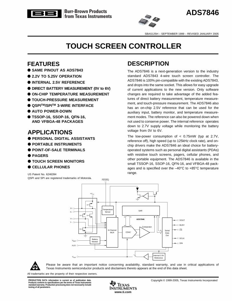
DESCRIPTIONThe ADS7846 is a next-generation version to the industrystandard ADS7843 4-wire touch screen controller. TheADS7846 is 100% pin-compatible with the existing ADS7843,and drops into the same socket. This allows for easy upgradeof current applications to the new version. Only softwarechanges are required to take advantage of the added fea-tures of direct battery measurement, temperature measure-ment, and touch-pressure measurement. The ADS7846 alsohas an on-chip 2.5V reference that can be used for theauxiliary input, battery monitor, and temperature measure-ment modes. The reference can also be powered down whennot used to conserve power. The internal reference operatesdown to 2.7V supply voltage while monitoring the batteryvoltage from 0V to 6V.
The low-power consumption of < 0.75mW (typ at 2.7V,reference off), high speed (up to 125kHz clock rate), and on-chip drivers make the ADS7846 an ideal choice for battery-operated systems such as personal digital assistants (PDAs)with resistive touch screens, pagers, cellular phones, andother portable equipment. The ADS7846 is available in thesmall TSSOP-16, SSOP-16, QFN-16, and VFBGA-48 pack-ages and is specified over the –40°C to +85°C temperaturerange.
CDAC
Internal 2.5VReference
SAR
ADS7846
Comparator
6-ChannelMUX
SerialDataOut
TemperatureSensor
BatteryMonitor
DOUT
BUSY
CS
DCLK
DIN
VBAT
AUX
VREF
+VCC
X+
X–
Y+
Y–
PENIRQ
ADS7846
SBAS125H – SEPTEMBER 1999 – REVISED JANUARY 2005
www.ti.com
PRODUCTION DATA information is current as of publication date.Products conform to specifications per the terms of Texas Instrumentsstandard warranty. Production processing does not necessarily includetesting of all parameters.
Copyright © 1999-2005, Texas Instruments Incorporated
US Patent No. 6246394QSPI and SPI are registered trademarks of Motorola.
®ADS7846
ADS7846
ADS7846
Please be aware that an important notice concerning availability, standard warranty, and use in critical applications ofTexas Instruments semiconductor products and disclaimers thereto appears at the end of this data sheet.
All trademarks are the property of their respective owners.
ADS78462SBAS125Hwww.ti.com
ABSOLUTE MAXIMUM RATINGS(1)
+VCC to GND ........................................................................ –0.3V to +6VAnalog Inputs to GND ............................................ –0.3V to +VCC + 0.3VDigital Inputs to GND ............................................. –0.3V to +VCC + 0.3VPower Dissipation .......................................................................... 250mWMaximum Junction Temperature ................................................... +150°COperating Temperature Range ........................................ –40°C to +85°CStorage Temperature Range ......................................... –65°C to +150°CLead Temperature (soldering, 10s) ............................................... +300°C
NOTE: (1) Stresses above these ratings can cause permanent damage.Exposure to absolute maximum conditions for extended periods may degradedevice reliability.
MAXIMUMINTEGRAL SPECIFIEDLINEARITY PACKAGE TEMPERATURE PACKAGE ORDERING
PRODUCT ERROR (LSB) PACKAGE-LEAD DESIGNATOR RANGE MARKING NUMBER
ADS7846E ±2 SSOP-16 DBQ –40°C to +85°C ADS7846E ADS7846E" " " " " " ADS7846E/2K5
ADS7846N ±2 TSSOP-16 PW –40°C to +85°C ADS7846N ADS7846N" " " " " " ADS7846N/2K5" " " " " " ADS7846N/2K5G4
ADS7846I ±2 VFBGA-48 GQC –40°C to +85°C ADS7846 ADS7846IGQCR
ADS7846I ±2 QFN-16 RGV –40°C to +85°C ADS7846 ADS7846IRGVT" " " " " " ADS7846IRGVR
NOTE: (1) For the most current package and ordering information, see the Package Option Addendum located at the end of this data sheet, or see the TI web siteat www.ti.com.
PACKAGE/ORDERING INFORMATION(1)
ELECTROSTATICDISCHARGE SENSITIVITY
This integrated circuit can be damaged by ESD. Texas Instru-ments recommends that all integrated circuits be handled withappropriate precautions. Failure to observe proper handlingand installation procedures can cause damage.
ESD damage can range from subtle performance degradationto complete device failure. Precision integrated circuits may bemore susceptible to damage because very small parametricchanges could cause the device not to meet its publishedspecifications.

ADS7846 3SBAS125H www.ti.com
ANALOG INPUTFull-Scale Input Span Positive Input-Negative Input 0 VREF VAbsolute Input Range Positive Input –0.2 +VCC + 0.2 V
Negative Input –0.2 +0.2 VCapacitance 25 pFLeakage Current 0.1 µA
SYSTEM PERFORMANCEResolution 12 BitsNo Missing Codes 11 BitsIntegral Linearity Error ±2 LSB(1)
Offset Error ±6 LSBGain Error External VREF ±4 LSBNoise Including Internal VREF 70 µVrmsPower-Supply Rejection 70 dB
SAMPLING DYNAMICSConversion Time 12 CLK CyclesAcquisition Time 3 CLK CyclesThroughput Rate 125 kHzMultiplexer Settling Time 500 nsAperture Delay 30 nsAperture Jitter 100 psChannel-to-Channel Isolation VIN = 2.5Vp-p at 50kHz 100 dB
SWITCH DRIVERSOn-Resistance
Y+, X+ 5 ΩY–, X– 6 Ω
Drive Current(2) Duration 100ms 50 mA
REFERENCE OUTPUTInternal Reference Voltage 2.45 2.50 2.55 VInternal Reference Drift 15 ppm/°CQuiescent Current 500 µA
REFERENCE INPUTRange 1.0 +VCC VInput Impedance SER/DFR = 0, PD1 = 0, 1 GΩ
Internal Reference OffInternal Reference On 250 Ω
BATTERY MONITORInput Voltage Range 0.5 6.0 VInput Impedance
Sampling Battery 10 kΩBattery Monitor Off 1 GΩ
Accuracy External VREF = 2.5V –2 +2 %Internal Reference –3 +3 %
TEMPERATURE MEASUREMENTTemperature Range –40 +85 °CResolution Differential Method(3) 1.6 °C
TEMP0(4) 0.3 °CAccuracy Differential Method(3) ±2 °C
TEMP0(4) ±3 °CDIGITAL INPUT/OUTPUTLogic Family CMOSLogic Levels, Except PENIRQ
VIH | IIH | ≤ +5µA +VCC • 0.7 +VCC + 0.3VIL | IIL | ≤ +5µA –0.3 +0.8 VVOH IOH = –250µA +VCC • 0.8 VVOL IOL = 250µA 0.4 V
PENIRQVOL TA = 0°C to +85°C, 50kΩ Pull-Up 0.8 V
Data Format Straight Binary
POWER-SUPPLY REQUIREMENTS+VCC
(5) Specified Performance 2.7 3.6 VOperating Range 2.2 5.25 V
Quiescent Current Internal Reference Off 280 650 µAInternal Reference On 780 µA
fSAMPLE = 12.5kHz 220 µAPower-Down Mode with 3 µA
CS = DCLK = DIN = +VCCPower Dissipation +VCC = +2.7V 1.8 mW
TEMPERATURE RANGESpecified Performance –40 +85 °C
NOTES: (1) LSB means least significant bit. With VREF equal to +2.5V, one LSB is 610µV. (2) Ensured by design, but not tested. Exceeding 50mA source currentmay result in device degradation. (3) Difference between TEMP0 and TEMP1 measurement. No calibration necessary. (4) Temperature drift is –2.1mV/°C.(5) ADS7846 operates down to 2.2V.
ADS7846E
PARAMETER CONDITIONS MIN TYP MAX UNITS
ELECTRICAL CHARACTERISTICSAt TA = –40°C to +85°C, +VCC = +2.7V, VREF = 2.5V internal voltage, fSAMPLE = 125kHz, fCLK = 16 • fSAMPLE = 2MHz, 12-bit mode, and digital inputs = GND or +VCC,unless otherwise noted.

ADS78464SBAS125Hwww.ti.com
PIN CONFIGURATION
Top View SSOP, TSSOP Top View VFBGA
1
2
3
4
5
6
7
8
+VCC
X+
Y+
X–
Y–
GND
VBAT
AUX
DCLK
CS
DIN
BUSY
DOUT
PENIRQ
+VCC
VREF
16
15
14
13
12
11
10
9
ADS7846
NC
NCA
21 3 4 5 6 7
DCLK
+VCC
+VCC
X+
Y+
PENIRQ
+VCC
VREF
AUX
CS DIN BUSY DOUT
X– Y– GND GND VBAT
NC
NC
NC
NC
NC
B
C
D
E
F
NC
NC
NC
NC
NC
NC
NC
NC
NC
NC
NC
NC
NC
NC
NC NC
NC
NC
NC
NC
NCNC
NCG
BUSY
DIN
CS
DCLK
AUX
VBAT
GND
Y–
1
2
3
4
12
11
10
9
ADS7846
DO
UT
PE
NIR
Q
+V
CC
VR
EF
16 15 14 13
+V
CC
X+
Y+
X–
5 6 7 8
Top View QFN
SSOP ANDTSSOP PIN # VFBGA PIN # QFN PIN # NAME DESCRIPTION
1 B1 and C1 5 +VCC Power Supply2 D1 6 X+ X+ Position Input3 E1 7 Y+ Y+ Position Input4 G2 8 X– X– Position Input5 G3 9 Y– Y– Position Input6 G4 and G5 10 GND Ground7 G6 11 VBAT Battery Monitor Input8 E7 12 AUX Auxiliary Input to ADC9 D7 13 VREF Voltage Reference Input/Output
10 C7 14 +VCC Digital I/O Power Supply11 B7 15 PENIRQ Pen Interrupt. Open anode output (requires 10kΩ to 100kΩ pull-up resistor externally).12 A6 16 DOUT Serial Data Output. Data is shifted on the falling edge of DCLK. This output is high
impedance when CS is high.13 A5 1 BUSY Busy Output. This output is high impedance when CS is high.14 A4 2 DIN Serial Data Input. If CS is low, data is latched on rising edge of DCLK.15 A3 3 CS Chip Select Input. Controls conversion timing and enables the serial input/output register.
CS high = power-down mode (ADC only).16 A2 4 DCLK External Clock Input. This clock runs the SAR conversion process and synchronizes serial data
I/O.
PIN DESCRIPTION

ADS7846 5SBAS125H www.ti.com
TYPICAL CHARACTERISTICSAt TA = +25°C, +VCC = +2.7V, VREF = External +2.5V, fSAMPLE = 125kHz, and fCLK = 16 • fSAMPLE = 2MHz, unless otherwise noted.
SUPPLY CURRENT vs TEMPERATURE
20–40 100–20 0 40
Temperature (°C)
Sup
ply
Cur
rent
(µA
)
400
350
300
250
200
150
10060 80
POWER-DOWN SUPPLY CURRENT vs TEMPERATURE
20–40 100–20 0 40
Temperature (°C)
Sup
ply
Cur
rent
(nA
)
140
120
100
80
60
40
2060 80
SUPPLY CURRENT vs +VCC
3.52.0 5.02.5 4.0
+VCC (V)
Sup
ply
Cur
rent
(µA
)
390
370
350
330
310
290
270
2504.53.0
fSAMPLE = 12.5kHz
MAXIMUM SAMPLE RATE vs +VCC
3.52.0 5.02.5 4.0
+VCC (V)
Sam
ple
Rat
e (H
z)
1M
100k
10k
1k4.53.0
CHANGE IN GAIN vs TEMPERATURE
20–40 100–20 0 40
Temperature (°C)
Del
ta fr
om +
25°C
(LS
B)
0.15
0.10
0.05
0
–0.05
–0.10
–0.1560 80
CHANGE IN OFFSET vs TEMPERATURE
20–40 100–20 0 40
Temperature (°C)
Del
ta fr
om +
25°C
(LS
B)
0.6
0.4
0.2
0
–0.2
–0.4
–0.660 80
ADS78466SBAS125Hwww.ti.com
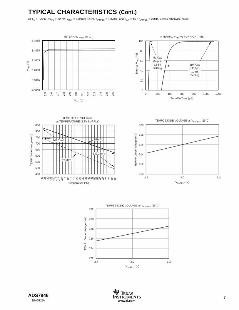
TYPICAL CHARACTERISTICS (Cont.)At TA = +25°C, +VCC = +2.7V, VREF = External +2.5V, fSAMPLE = 125kHz, and fCLK = 16 • fSAMPLE = 2MHz, unless otherwise noted.
REFERENCE CURRENT vs SAMPLE RATE
750 12525 50 100
Sample Rate (kHz)
Ref
eren
ce C
urre
nt (
µA)
14
12
10
8
6
4
2
0
REFERENCE CURRENT vs TEMPERATURE
20–40 100–20 0 40
Temperature (°C)
Ref
eren
ce C
urre
nt (
µA)
18
16
14
12
10
8
660 80
SWITCH-ON RESISTANCE vs TEMPERATURE(X+, Y+: +VCC to Pin; X–, Y–: Pin to GND)
20–40 100–20
X+ Y+
Y–X–
40
Temperature (°C)
RO
N (Ω
)
1
8
7
6
5
4
3
2
60 800
2.4920
2.4915
2.4910
2.4905
2.4900
2.4895
2.4890
2.4885
2.4880
2.4875
Inte
rnal
VR
EF (
V)
Temperature (°C)
INTERNAL VREF vs TEMPERATURE
–40
–35
–30
–25
–20
–15
–10
–05 0 05 10 15 20 25 30 35 40 45 50 55 60 65 70 75 80 85
SWITCH-ON RESISTANCE vs +VCC(X+, Y+: +VCC to Pin; X–, Y–: Pin to GND)
3.52.0 5.02.5
X+Y+
Y–
X–
4.0
+VCC (V)
RO
N (Ω
)
1
8
7
6
5
4
3
2
4.53.0
2.0
1.8
1.6
1.4
1.2
1.0
0.8
0.6
0.4
0.2
0
Err
or (
LSB
)
20 40 60 80 100 120 140 160 180 200Sampling Rate (kHz)
MAXIMUM SAMPLING RATE vs RIN
INL: R = 2kINL: R = 500DNL: R = 2kDNL: R = 500
ADS7846 7SBAS125H www.ti.com
TYPICAL CHARACTERISTICS (Cont.)At TA = +25°C, +VCC = +2.7V, VREF = External +2.5V, fSAMPLE = 125kHz, and fCLK = 16 • fSAMPLE = 2MHz, unless otherwise noted.
2.4865
2.4860
2.4855
2.4850
2.4845
2.4840
VR
EF (
V)
2.5
2.6
2.7
2.8
2.9
3.0
3.1
3.2
3.3
3.4
3.5
3.6
VCC (V)
INTERNAL VREF vs VCC
850
800
750
700
650
600
550
500
450
TE
MP
Dio
de V
olta
ge (
mV
)
Temperature (°C)
–40
–35
–30
–25
–20
–15
–10
–05 0 05 10 15 20 25 30 35 40 45 50 55 60 65 70 75 80 85
TEMP DIODE VOLTAGEvs TEMPERATURE (2.7V SUPPLY)
102.7mV
132.25mV
TEMP0
TEMP1
100
80
60
40
20
0
Inte
rnal
VR
EF (
%)
0 200 400 600 800 1000 1200
INTERNAL VREF vs TURN-ON TIME
Turn-On Time (µS)
1µF Cap(1110µS)
12-BitSettling
No Cap(52µS)12-Bit
Settling
620
618
616
614
612
6102.7 3.0 3.3
VSUPPLY (V)
TEMP0 DIODE VOLTAGE vs VSUPPLY (25°C)
TE
MP
0 D
iode
Vol
tage
(m
V)
732
730
728
726
724
7222.7 3.0 3.3
VSUPPLY (V)
TEMP1 DIODE VOLTAGE vs VSUPPLY (25°C)
TE
MP
1 D
iode
Vol
tage
(m
V)
ADS78468SBAS125Hwww.ti.com
THEORY OF OPERATIONThe ADS7846 is a classic successive approximation register(SAR) analog-to-digital converter (ADC). The architecture isbased on capacitive redistribution which inherently includesa sample-and-hold function. The converter is fabricated on a0.6µm CMOS process.
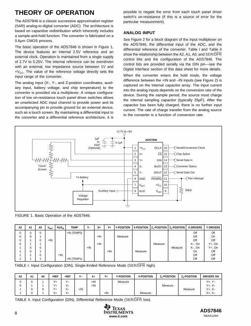
The basic operation of the ADS7846 is shown in Figure 1.The device features an internal 2.5V reference and anexternal clock. Operation is maintained from a single supplyof 2.7V to 5.25V. The internal reference can be overdrivenwith an external, low impedance source between 1V and+VCC. The value of the reference voltage directly sets theinput range of the converter.
The analog input (X-, Y-, and Z-position coordinates, auxil-iary input, battery voltage, and chip temperature) to theconverter is provided via a multiplexer. A unique configura-tion of low on-resistance touch panel driver switches allowsan unselected ADC input channel to provide power and itsaccompanying pin to provide ground for an external device,such as a touch screen. By maintaining a differential input tothe converter and a differential reference architecture, it is
possible to negate the error from each touch panel driverswitch’s on-resistance (if this is a source of error for theparticular measurement).
ANALOG INPUT
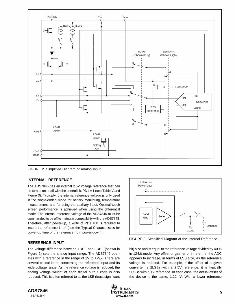
See Figure 2 for a block diagram of the input multiplexer onthe ADS7846, the differential input of the ADC, and thedifferential reference of the converter. Table I and Table IIshow the relationship between the A2, A1, A0, and SER/DFRcontrol bits and the configuration of the ADS7846. Thecontrol bits are provided serially via the DIN pin—see theDigital Interface section of this data sheet for more details.
When the converter enters the hold mode, the voltagedifference between the +IN and –IN inputs (see Figure 2) iscaptured on the internal capacitor array. The input currentinto the analog inputs depends on the conversion rate of thedevice. During the sample period, the source must chargethe internal sampling capacitor (typically 25pF). After thecapacitor has been fully charged, there is no further inputcurrent. The rate of charge transfer from the analog sourceto the converter is a function of conversion rate.
FIGURE 1. Basic Operation of the ADS7846.
A2 A1 A0 VBAT AUXIN TEMP Y– X+ Y+ Y-POSITION X-POSITION Z1-POSITION Z2-POSITION X-DRIVERS Y-DRIVERS
0 0 0 +IN (TEMP0) Off Off0 0 1 +IN Measure Off On0 1 0 +IN Off Off0 1 1 +IN Measure X–, On Y+, On1 0 0 +IN Measure X–, On Y+, On1 0 1 +IN Measure On Off1 1 0 +IN Off Off1 1 1 +IN (TEMP1) Off Off
TABLE I. Input Configuration (DIN), Single-Ended Reference Mode (SER/DFR high).
TABLE II. Input Configuration (DIN), Differential Reference Mode (SER/DFR low).
A2 A1 A0 +REF –REF Y– X+ Y+ Y-POSITION X-POSITION Z1-POSITION Z2-POSITION DRIVERS ON
0 0 1 Y+ Y– +IN Measure Y+, Y–0 1 1 Y+ X– +IN Measure Y+, X–1 0 0 Y+ X– +IN Measure Y+, X–1 0 1 X+ X– +IN Measure X+, X–
+VCC
X+
Y+
X–
Y–
GND
VBAT
AUX
1
2
3
4
5
6
7
8
16
15
14
13
12
11
10
9
DCLK
CS
DIN
BUSY
DOUT
PENIRQ
+VCC
VREF
Serial/Conversion Clock
Chip Select
Serial Data In
Converter Status
Serial Data Out
+1µF
to 10µF
(Optional)
+2.7V to +5V
ADS7846
Auxiliary Input
To Battery
VoltageRegulator
Touch Screen
0.1µF
Pen Interrupt
50kΩ
ADS7846 9SBAS125H www.ti.com
INTERNAL REFERENCE
The ADS7846 has an internal 2.5V voltage reference that canbe turned on or off with the control bit, PD1 = 1 (see Table V andFigure 3). Typically, the internal reference voltage is only usedin the single-ended mode for battery monitoring, temperaturemeasurement, and for using the auxiliary input. Optimal touchscreen performance is achieved when using the differentialmode. The internal reference voltage of the ADS7846 must becommanded to be off to maintain compatibility with the ADS7843.Therefore, after power-up, a write of PD1 = 0 is required toinsure the reference is off (see the Typical Characteristics forpower-up time of the reference from power-down).
REFERENCE INPUT
The voltage difference between +REF and –REF (shown inFigure 2) sets the analog input range. The ADS7846 oper-ates with a reference in the range of 1V to +VCC. There areseveral critical items concerning the reference input and itswide voltage range. As the reference voltage is reduced, theanalog voltage weight of each digital output code is alsoreduced. This is often referred to as the LSB (least significant
bit) size and is equal to the reference voltage divided by 4096in 12-bit mode. Any offset or gain error inherent in the ADCappears to increase, in terms of LSB size, as the referencevoltage is reduced. For example, if the offset of a givenconverter is 2LSBs with a 2.5V reference, it is typically5LSBs with a 1V reference. In each case, the actual offset ofthe device is the same, 1.22mV. With a lower reference
FIGURE 2. Simplified Diagram of Analog Input.
Converter
–REF
+REF+IN
–IN
VBAT
AUX
BatteryOn
GND
A2-A0(Shown 001B)
2.5VReference
Ref On/Off
SER/DFR(Shown High)
X+
X–
+VCC
TEMP1
PENIRQ
Y+
Y–
VREF
TEMP0
7.5kΩ
2.5kΩ
BufferBandGap
ReferencePower Down
ToCDAC
Optional
VREF
FIGURE 3. Simplified Diagram of the Internal Reference.
ADS784610SBAS125Hwww.ti.com
voltage, more care must be taken to provide a clean layoutincluding adequate bypassing, a clean (low-noise, low-ripple)power supply, a low-noise reference (if an external referenceis used), and a low-noise input signal.
The voltage into the VREF input directly drives the capacitordigital-to-analog converter (CDAC) portion of the ADS7846.Therefore, the input current is very low (typically < 13µA).
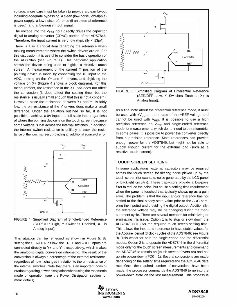
There is also a critical item regarding the reference whenmaking measurements where the switch drivers are on. Forthis discussion, it is useful to consider the basic operation ofthe ADS7846 (see Figure 1). This particular applicationshows the device being used to digitize a resistive touchscreen. A measurement of the current Y position of thepointing device is made by connecting the X+ input to theADC, turning on the Y+ and Y– drivers, and digitizing thevoltage on X+ (Figure 4 shows a block diagram). For thismeasurement, the resistance in the X+ lead does not affectthe conversion (it does affect the settling time, but theresistance is usually small enough that this is not a concern).However, since the resistance between Y+ and Y– is fairlylow, the on-resistance of the Y drivers does make a smalldifference. Under the situation outlined so far, it is notpossible to achieve a 0V input or a full-scale input regardlessof where the pointing device is on the touch screen, becausesome voltage is lost across the internal switches. In addition,the internal switch resistance is unlikely to track the resis-tance of the touch screen, providing an additional source of error.
FIGURE 4. Simplified Diagram of Single-Ended Reference(SER/DFR High, Y Switches Enabled, X+ isAnalog Input).
This situation can be remedied as shown in Figure 5. Bysetting the SER/DFR bit low, the +REF and –REF inputs areconnected directly to Y+ and Y–, respectively, which makesthe analog-to-digital conversion ratiometric. The result of theconversion is always a percentage of the external resistance,regardless of how it changes in relation to the on-resistance ofthe internal switches. Note that there is an important consid-eration regarding power dissipation when using the ratiometricmode of operation (see the Power Dissipation section formore details).
FIGURE 5. Simplified Diagram of Differential Reference(SER/DFR Low, Y Switches Enabled, X+ isAnalog Input).
Converter
+IN+REF
Y+
+VCC
X+
Y–
GND
–REF–IN
As a final note about the differential reference mode, it mustbe used with +VCC as the source of the +REF voltage andcannot be used with VREF. It is possible to use a highprecision reference on VREF and single-ended referencemode for measurements which do not need to be ratiometric.In some cases, it is possible to power the converter directlyfrom a precision reference. Most references can provideenough power for the ADS7846, but might not be able tosupply enough current for the external load (such as aresistive touch screen).
TOUCH SCREEN SETTLING
In some applications, external capacitors may be requiredacross the touch screen for filtering noise picked up by thetouch screen (for example, noise generated by the LCD panelor backlight circuitry). These capacitors provide a low-passfilter to reduce the noise, but cause a settling time requirementwhen the panel is touched that typically shows up as a gainerror. The problem is that the input and/or reference has notsettled to the final steady-state value prior to the ADC sam-pling the input(s) and providing the digital output. Additionally,the reference voltage may still be changing during the mea-surement cycle. There are several methods for minimizing oreliminating this issue. Option 1 is to stop or slow down theADS7846 DCLK for the required touch screen settling time.This allows the input and reference to have stable values forthe Acquire period (3 clock cycles of the ADS7846; see Figure9). This works for both the single-ended and the differentialmodes. Option 2 is to operate the ADS7846 in the differentialmode only for the touch screen measurements and commandthe ADS7846 to remain on (touch screen drivers on) and notgo into power-down (PD0 = 1). Several conversions are madedepending on the settling time required and the ADS7846 datarate. Once the required number of conversions have beenmade, the processor commands the ADS7846 to go into thepower-down state on the last measurement. This process is
Converter
+IN+REF
Y+
+VCC VREF
X+
Y–
GND
–REF–IN
ADS7846 11SBAS125H www.ti.com
required for X-position, Y-position, and Z-position measure-ments. Option 3 is to operate in the 15 Clock-per-Conversionmode which overlaps the analog-to-digital conversions andmaintains the touch screen drivers on until commanded tostop by the processor (see Figure 12).
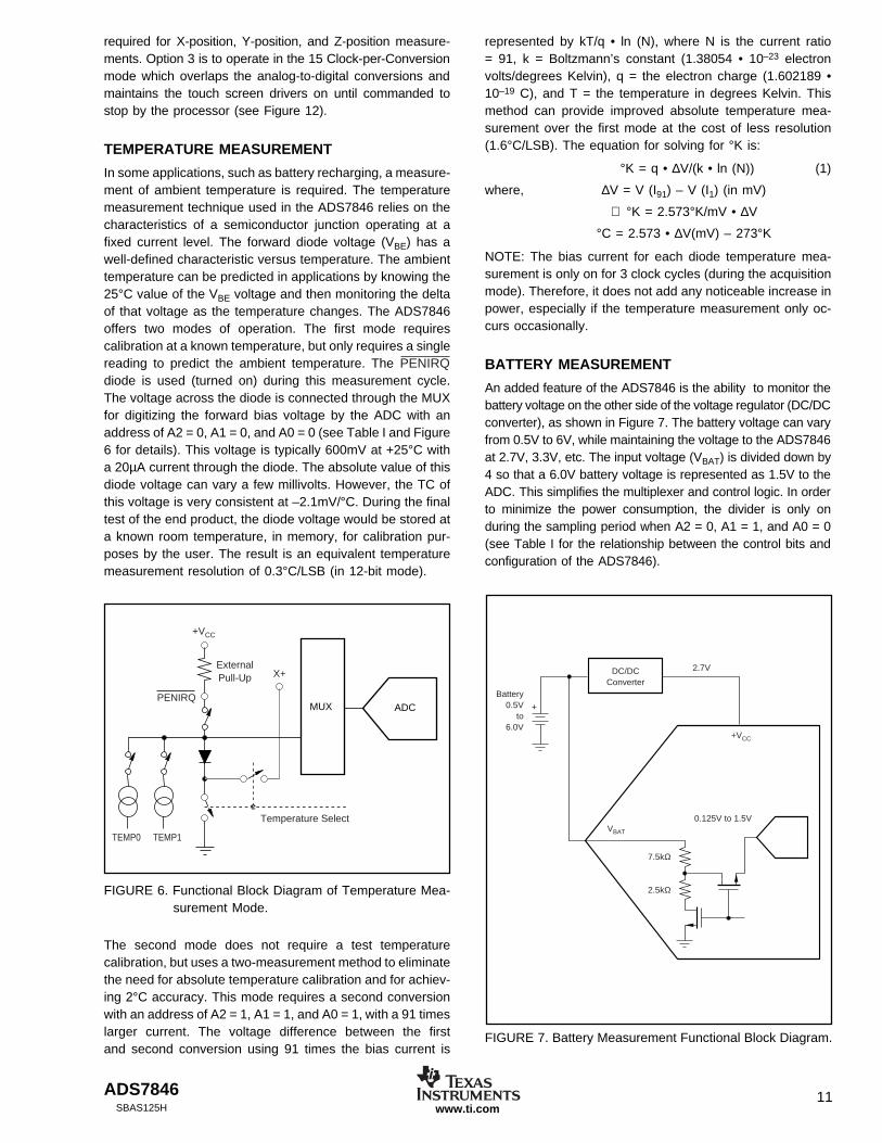
TEMPERATURE MEASUREMENT
In some applications, such as battery recharging, a measure-ment of ambient temperature is required. The temperaturemeasurement technique used in the ADS7846 relies on thecharacteristics of a semiconductor junction operating at afixed current level. The forward diode voltage (VBE) has awell-defined characteristic versus temperature. The ambienttemperature can be predicted in applications by knowing the25°C value of the VBE voltage and then monitoring the deltaof that voltage as the temperature changes. The ADS7846offers two modes of operation. The first mode requirescalibration at a known temperature, but only requires a singlereading to predict the ambient temperature. The PENIRQdiode is used (turned on) during this measurement cycle.The voltage across the diode is connected through the MUXfor digitizing the forward bias voltage by the ADC with anaddress of A2 = 0, A1 = 0, and A0 = 0 (see Table I and Figure6 for details). This voltage is typically 600mV at +25°C witha 20µA current through the diode. The absolute value of thisdiode voltage can vary a few millivolts. However, the TC ofthis voltage is very consistent at –2.1mV/°C. During the finaltest of the end product, the diode voltage would be stored ata known room temperature, in memory, for calibration pur-poses by the user. The result is an equivalent temperaturemeasurement resolution of 0.3°C/LSB (in 12-bit mode).
FIGURE 7. Battery Measurement Functional Block Diagram.
represented by kT/q • ln (N), where N is the current ratio= 91, k = Boltzmann’s constant (1.38054 • 10–23 electronvolts/degrees Kelvin), q = the electron charge (1.602189 •10–19 C), and T = the temperature in degrees Kelvin. Thismethod can provide improved absolute temperature mea-surement over the first mode at the cost of less resolution(1.6°C/LSB). The equation for solving for °K is:
°K = q • ∆V/(k • ln (N)) (1)
where, ∆V = V (I91) – V (I1) (in mV)
∴ °K = 2.573°K/mV • ∆V
°C = 2.573 • ∆V(mV) – 273°K
NOTE: The bias current for each diode temperature mea-surement is only on for 3 clock cycles (during the acquisitionmode). Therefore, it does not add any noticeable increase inpower, especially if the temperature measurement only oc-curs occasionally.
BATTERY MEASUREMENT
An added feature of the ADS7846 is the ability to monitor thebattery voltage on the other side of the voltage regulator (DC/DCconverter), as shown in Figure 7. The battery voltage can varyfrom 0.5V to 6V, while maintaining the voltage to the ADS7846at 2.7V, 3.3V, etc. The input voltage (VBAT) is divided down by4 so that a 6.0V battery voltage is represented as 1.5V to theADC. This simplifies the multiplexer and control logic. In orderto minimize the power consumption, the divider is only onduring the sampling period when A2 = 0, A1 = 1, and A0 = 0(see Table I for the relationship between the control bits andconfiguration of the ADS7846).
+VCC
VBAT
7.5kΩ
2.5kΩ
DC/DCConverter
Battery0.5V
to6.0V
0.125V to 1.5V
2.7V
+
FIGURE 6. Functional Block Diagram of Temperature Mea-surement Mode.
ADCMUXPENIRQ
+VCC
ExternalPull-Up X+
Temperature Select
TEMP0 TEMP1
The second mode does not require a test temperaturecalibration, but uses a two-measurement method to eliminatethe need for absolute temperature calibration and for achiev-ing 2°C accuracy. This mode requires a second conversionwith an address of A2 = 1, A1 = 1, and A0 = 1, with a 91 timeslarger current. The voltage difference between the firstand second conversion using 91 times the bias current is
ADS784612SBAS125Hwww.ti.com
The first eight clock cycles are used to provide the controlbyte via the DIN pin. When the converter has enoughinformation about the following conversion to set the inputmultiplexer and reference inputs appropriately, the converterenters the acquisition (sample) mode and, if needed,the touch panel drivers are turned on. After three moreclock cycles, the control byte is complete and the converterenters the conversion mode. At this point, the input
FIGURE 9. Conversion Timing, 24 Clocks-per-Conversion, 8-bit Bus Interface. No DCLK delay required with dedicatedserial port.
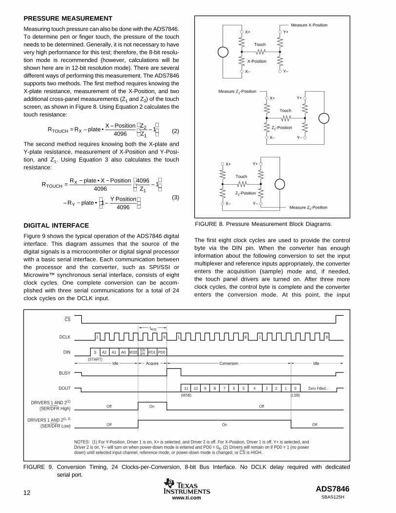
PRESSURE MEASUREMENT
Measuring touch pressure can also be done with the ADS7846.To determine pen or finger touch, the pressure of the touchneeds to be determined. Generally, it is not necessary to havevery high performance for this test; therefore, the 8-bit resolu-tion mode is recommended (however, calculations will beshown here are in 12-bit resolution mode). There are severaldifferent ways of performing this measurement. The ADS7846supports two methods. The first method requires knowing theX-plate resistance, measurement of the X-Position, and twoadditional cross-panel measurements (Z1 and Z2) of the touchscreen, as shown in Figure 8. Using Equation 2 calculates thetouch resistance:
R R plateX Position Z
ZTOUCH X=
– •–
–4096
12
1 (2)
The second method requires knowing both the X-plate andY-plate resistance, measurement of X-Position and Y-Posi-tion, and Z1. Using Equation 3 also calculates the touchresistance:
RR plate • X Position
40964096
Z– 1
–R plateY Position
4096
TOUCHX
1
Y
= − −
− •
1– (3)
DIGITAL INTERFACE
Figure 9 shows the typical operation of the ADS7846 digitalinterface. This diagram assumes that the source of thedigital signals is a microcontroller or digital signal processorwith a basic serial interface. Each communication betweenthe processor and the converter, such as SPI/SSI orMicrowire™ synchronous serial interface, consists of eightclock cycles. One complete conversion can be accom-plished with three serial communications for a total of 24clock cycles on the DCLK input.
FIGURE 8. Pressure Measurement Block Diagrams.
tACQ
AcquireIdle Conversion Idle
1DCLK
CS
8 1
11DOUT
BUSY
DRIVERS 1 AND 2(1)
(SER/DFR High)
DRIVERS 1 AND 2(1, 2)
(SER/DFR Low)
(MSB)
(START)
(LSB)
A2S
On
On
Off Off
Off Off
DIN A1 A0 MODE SER/DFR PD1 PD0
10 9 8 7 6 5 4 3 2 1 0 Zero Filled...
8 1 8
NOTES: (1) For Y-Position, Driver 1 is on, X+ is selected, and Driver 2 is off. For X-Position, Driver 1 is off, Y+ is selected, and Driver 2 is on. Y– will turn on when power-down mode is entered and PD0 = 0B. (2) Drivers will remain on if PD0 = 1 (no power down) until selected input channel, reference mode, or power-down mode is changed, or CS is HIGH.
X-Position
Measure X-Position
Measure Z1-Position
Touch
X+ Y+
X– Y–
Z1-Position
Touch
X+ Y+
Y–X–
Measure Z2-Position
Z2-Position
Touch
X+ Y+
Y–X–

ADS7846 13SBAS125H www.ti.com
sample-and-hold goes into the hold mode and the touchpanel drivers turn off (in single-ended mode). The next 12clock cycles accomplish the actual analog-to-digital conver-sion. If the conversion is ratiometric (SER/DFR = 0), thedrivers are on during the conversion and a 13th clock cycleis needed for the last bit of the conversion result. Three moreclock cycles are needed to complete the last byte (DOUT willbe low), which are ignored by the converter.
Control Byte
The control byte (on DIN), as shown in Table III, provides thestart conversion, addressing, ADC resolution, configuration,and power-down of the ADS7846. Figure 9 and Tables IIIand IV give detailed information regarding the order anddescription of these control bits within the control byte.
SER/DFR—The SER/DFR bit controls the reference mode,either single-ended (high) or differential (low). The differentialmode is also referred to as the ratiometric conversion modeand is preferred for X-Position, Y-Position, and Pressure-Touch measurements for optimum performance. The refer-ence is derived from the voltage at the switch drivers, whichis almost the same as the voltage to the touch screen. In thiscase a reference voltage is not needed, as the referencevoltage to the ADC is the voltage across the touch screen. Inthe single-ended mode, the converter reference voltage isalways the difference between the VREF and GND pins (seeTables I and II, and Figures 2 through 5 for further informa-tion).
If X-Position, Y-Position, and Pressure-Touch are measuredin the single-ended mode, an external reference voltage isneeded. The ADS7846 should also be powered from theexternal reference. Caution must be observed when usingthe single-ended mode such that the input voltage to theADC does not exceed the internal reference voltage, espe-cially if the supply voltage is greater than 2.7V.
NOTE: The differential mode can only be used for X-Position,Y-Position, and Pressure-Touch measurements. All othermeasurements require the single-ended mode.
PD0 and PD1—Table V describes the power-down and theinternal reference voltage configurations. The internal refer-ence voltage can be turned on or off independently of theADC. This can allow extra time for the internal referencevoltage to settle to the final value prior to making a conver-sion. Make sure to also allow this extra wake-up time if theinternal reference is powered down. The ADC requires nowake-up time and can be instantaneously used. Also notethat the status of the internal reference power-down islatched into the part (internally) with BUSY going high.Therefore, in order to turn the reference off, an additionalwrite to the ADS7846 is required after the channel is con-verted.
Bit 7 Bit 0(MSB) Bit 6 Bit 5 Bit 4 Bit 3 Bit 2 Bit 1 (LSB)
S A2 A1 A0 MODE SER/DFR PD1 PD0
TABLE III. Order of the Control Bits in the Control Byte.
BIT NAME DESCRIPTION
7 S Start Bit. Control byte starts with first high bit on DIN.A new control byte can start every 15th clock cyclein 12-bit conversion mode or every 11th clock cyclein 8-bit conversion mode (see Figure 12).
6-4 A2-A0 Channel Select Bits. Along with the SER/DFR bit,these bits control the setting of the multiplexer input,touch driver switches, and reference inputs (seeTables I and II).
3 MODE 12-Bit/8-Bit Conversion Select Bit. This bit controlsthe number of bits for the next conversion: 12-bits(low) or 8-bits (high).
2 SER/DFR Single-Ended/Differential Reference Select Bit. Alongwith bits A2-A0, this bit controls the setting of themultiplexer input, touch driver switches, and referenceinputs (see Tables I and I).
1-0 PD1-PD0 Power-Down Mode Select Bits. See Table V fordetails.
TABLE IV. Descriptions of the Control Bits within the ControlByte.
Initiate START—The first bit, the S bit, must always be highand initiates the start of the control byte. The ADS7846ignores inputs on the DIN pin until the start bit is detected.
Addressing—The next three bits (A2, A1, and A0) select theactive input channel(s) of the input multiplexer (see Tables I,II, and Figure 2), touch screen drivers, and the referenceinputs.
MODE—The mode bit sets the resolution of the ADC. Withthis bit low, the next conversion has 12 bits of resolution; withthis bit high, the next conversion has 8 bits of resolution.
PD1 PD0 PENIRQ DESCRIPTION
0 0 Enabled Power-Down Between Conversions. When eachconversion is finished, the converter enters alow-power mode. At the start of the next conver-sion, the device instantly powers up to full power.There is no need for additional delays to assurefull operation and the very first conversion isvalid. The Y– switch is on when in power-down.
0 1 Disabled Reference is off and ADC is on.
1 0 Enabled Reference is on and ADC is off.
1 1 Disabled Device is always powered. Reference is on andADC is on.
TABLE V. Power-Down and Internal Reference Selection.

ADS784614SBAS125Hwww.ti.com
16 Clocks-per-Conversion
The control bits for conversion n + 1 can be overlapped withconversion n to allow for a conversion every 16 clock cycles,as shown in Figure 10. This figure also shows possible serialcommunication occurring with other serial peripherals be-tween each byte transfer from the processor to the converter.This is possible provided that each conversion completeswithin 1.6ms of starting. Otherwise, the signal that is cap-tured on the input sample-and-hold may droop enough toaffect the conversion result. Note that the ADS7846 is fullypowered while other serial communications are taking placeduring a conversion.
Digital Timing
Figures 9, 11, and Table VI provide detailed timing for thedigital interface of the ADS7846.
SYMBOL DESCRIPTION MIN TYP MAX UNITS
tACQ Acquisition Time 1.5 µs
tDS DIN Valid Prior to DCLK Rising 100 ns
tDH DIN Hold After DCLK High 10 ns
tDO DCLK Falling to DOUT Valid 200 ns
tDV CS Falling to DOUT Enabled 200 ns
tTR CS Rising to DOUT Disabled 200 ns
tCSS CS Falling to First DCLK Rising 100 ns
tCSH CS Rising to DCLK Ignored 0 ns
tCH DCLK High 200 ns
tCL DCLK Low 200 ns
tBD DCLK Falling to BUSY Rising 200 ns
tBDV CS Falling to BUSY Enabled 200 ns
tBTR CS Rising to BUSY Disabled 200 ns
TABLE VI. Timing Specifications (+VCC = +2.7V and Above,TA = –40°C to +85°C, CLOAD = 50pF).
PD0
tBDV
tDH
tCH
tCL
tDS
tCSS
tDV
tBD tBD
tTR
tBTR
tD0 tCSH
DCLK
CS
11DOUT
BUSY
DIN
10
FIGURE 11. Detailed Timing Diagram.
FIGURE 10. Conversion Timing, 16 Clocks-per-Conversion, 8-Bit Bus Interface. No DCLK delay required with dedicatedserial port.
1
DCLK
CS
8 1
11DOUT
BUSY
SDIN
Control Bits
S
Control Bits
10 9 8 7 6 5 4 3 2 1 0 11 10 9
8 1 18

ADS7846 15SBAS125H www.ti.com
15 Clocks-per-Conversion
Figure 12 provides the fastest way to clock the ADS7846.This method does not work with the serial interface of mostmicrocontrollers and digital signal processors, as they aregenerally not capable of providing 15 clock cycles per serialtransfer. However, this method can be used with field pro-grammable gate arrays (FPGAs) or application specific inte-grated circuits (ASICs). Note that this effectively increasesthe maximum conversion rate of the converter beyond thevalues given in the specification tables, which assume 16clock cycles per conversion.
Data Format
The ADS7846 output data is in Straight Binary format asshown in Figure 13. This figure shows the ideal output codefor the given input voltage and does not include the effectsof offset, gain, or noise.
8-Bit Conversion
The ADS7846 provides an 8-bit conversion mode that can beused when faster throughput is needed and the digital resultis not as critical. By switching to the 8-bit mode, a conversionis complete four clock cycles earlier. Not only does this shorteneach conversion by four bits (25% faster throughput), but eachconversion can actually occur at a faster clock rate. This isbecause the internal settling time of the ADS7846 is not ascritical—settling to better than 8 bits is all that is needed. Theclock rate can be as much as 50% faster. The faster clock rateand fewer clock cycles combine to provide a 2x increase inconversion rate.
POWER DISSIPATION
There are two major power modes for the ADS7846: full power(PD0 = 1B) and auto power-down (PD0 = 0B). When operatingat full speed and 16 clocks-per-conversion (see Figure 10), theADS7846 spends most of the time acquiring or converting.There is little time for auto power-down, assuming that thismode is active. Therefore, the difference between full-powermode and auto power-down is negligible. If the conversionrate is decreased by slowing the frequency of the DCLK input,the two modes remain approximately equal. However, if theDCLK frequency is kept at the maximum rate during a conver-sion but conversions are done less often, the differencebetween the two modes is dramatic.
FIGURE 12. Maximum Conversion Rate, 15 Clocks-per-Conversion.
1
DCLK
CS
11DOUT
BUSY
A2SDIN A1 A0 MODESGL/DIF PD1 PD0
10 9 8 7 6 5 4 3 2 1 0 11 10 9 8 7 Tri-State
A1 A0
15 1 15
Power Down
1
A2S A1 A0 MODE PD1 PD0 A2SSGL/DIF
FIGURE 13. Ideal Input Voltages and Output Codes.
Out
put C
ode
0V
FS = Full-Scale Voltage = VREF(1)
1LSB = VREF(1)/4096
FS – 1LSB
11...111
11...110
11...101
00...010
00...001
00...000
1LSB
NOTES: (1) Reference voltage at converter: +REF – (–REF), see Figure 2. (2) Input voltage at converter, after multiplexer: +IN – (–IN), see Figure 2.
Input Voltage(2) (V)
ADS784616SBAS125Hwww.ti.com
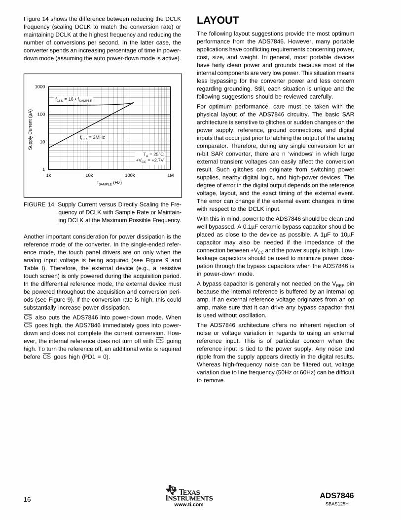
Figure 14 shows the difference between reducing the DCLKfrequency (scaling DCLK to match the conversion rate) ormaintaining DCLK at the highest frequency and reducing thenumber of conversions per second. In the latter case, theconverter spends an increasing percentage of time in power-down mode (assuming the auto power-down mode is active).
LAYOUTThe following layout suggestions provide the most optimumperformance from the ADS7846. However, many portableapplications have conflicting requirements concerning power,cost, size, and weight. In general, most portable deviceshave fairly clean power and grounds because most of theinternal components are very low power. This situation meansless bypassing for the converter power and less concernregarding grounding. Still, each situation is unique and thefollowing suggestions should be reviewed carefully.
For optimum performance, care must be taken with thephysical layout of the ADS7846 circuitry. The basic SARarchitecture is sensitive to glitches or sudden changes on thepower supply, reference, ground connections, and digitalinputs that occur just prior to latching the output of the analogcomparator. Therefore, during any single conversion for ann-bit SAR converter, there are n ‘windows’ in which largeexternal transient voltages can easily affect the conversionresult. Such glitches can originate from switching powersupplies, nearby digital logic, and high-power devices. Thedegree of error in the digital output depends on the referencevoltage, layout, and the exact timing of the external event.The error can change if the external event changes in timewith respect to the DCLK input.
With this in mind, power to the ADS7846 should be clean andwell bypassed. A 0.1µF ceramic bypass capacitor should beplaced as close to the device as possible. A 1µF to 10µFcapacitor may also be needed if the impedance of theconnection between +VCC and the power supply is high. Low-leakage capacitors should be used to minimize power dissi-pation through the bypass capacitors when the ADS7846 isin power-down mode.
A bypass capacitor is generally not needed on the VREF pinbecause the internal reference is buffered by an internal opamp. If an external reference voltage originates from an opamp, make sure that it can drive any bypass capacitor thatis used without oscillation.
The ADS7846 architecture offers no inherent rejection ofnoise or voltage variation in regards to using an externalreference input. This is of particular concern when thereference input is tied to the power supply. Any noise andripple from the supply appears directly in the digital results.Whereas high-frequency noise can be filtered out, voltagevariation due to line frequency (50Hz or 60Hz) can be difficultto remove.
10k 100k1k 1M
fSAMPLE (Hz)
Sup
ply
Cur
rent
(µA
)
100
10
1
1000
fCLK = 2MHz
fCLK = 16 • fSAMPLE
TA = 25°C+VCC = +2.7V
FIGURE 14. Supply Current versus Directly Scaling the Fre-quency of DCLK with Sample Rate or Maintain-ing DCLK at the Maximum Possible Frequency.
Another important consideration for power dissipation is thereference mode of the converter. In the single-ended refer-ence mode, the touch panel drivers are on only when theanalog input voltage is being acquired (see Figure 9 andTable I). Therefore, the external device (e.g., a resistivetouch screen) is only powered during the acquisition period.In the differential reference mode, the external device mustbe powered throughout the acquisition and conversion peri-ods (see Figure 9). If the conversion rate is high, this couldsubstantially increase power dissipation.
CS also puts the ADS7846 into power-down mode. WhenCS goes high, the ADS7846 immediately goes into power-down and does not complete the current conversion. How-ever, the internal reference does not turn off with CS goinghigh. To turn the reference off, an additional write is requiredbefore CS goes high (PD1 = 0).
ADS7846 17SBAS125H www.ti.com
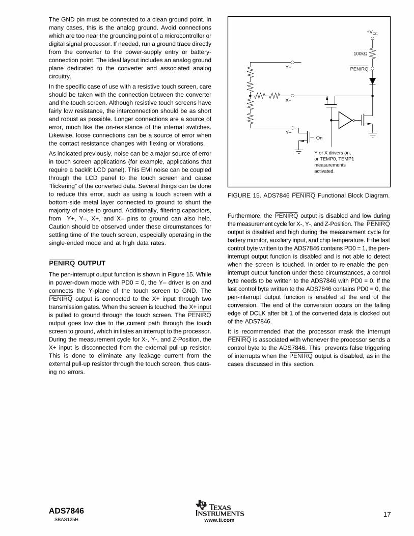
FIGURE 15. ADS7846 PENIRQ Functional Block Diagram.
PENIRQ
+VCC
100kΩ
On
Y or X drivers on,or TEMP0, TEMP1measurementsactivated.
Y+
X+
Y–
The GND pin must be connected to a clean ground point. Inmany cases, this is the analog ground. Avoid connectionswhich are too near the grounding point of a microcontroller ordigital signal processor. If needed, run a ground trace directlyfrom the converter to the power-supply entry or battery-connection point. The ideal layout includes an analog groundplane dedicated to the converter and associated analogcircuitry.
In the specific case of use with a resistive touch screen, careshould be taken with the connection between the converterand the touch screen. Although resistive touch screens havefairly low resistance, the interconnection should be as shortand robust as possible. Longer connections are a source oferror, much like the on-resistance of the internal switches.Likewise, loose connections can be a source of error whenthe contact resistance changes with flexing or vibrations.
As indicated previously, noise can be a major source of errorin touch screen applications (for example, applications thatrequire a backlit LCD panel). This EMI noise can be coupledthrough the LCD panel to the touch screen and cause“flickering” of the converted data. Several things can be doneto reduce this error, such as using a touch screen with abottom-side metal layer connected to ground to shunt themajority of noise to ground. Additionally, filtering capacitors,from Y+, Y–, X+, and X– pins to ground can also help.Caution should be observed under these circumstances forsettling time of the touch screen, especially operating in thesingle-ended mode and at high data rates.
PENIRQ OUTPUT
The pen-interrupt output function is shown in Figure 15. Whilein power-down mode with PD0 = 0, the Y– driver is on andconnects the Y-plane of the touch screen to GND. ThePENIRQ output is connected to the X+ input through twotransmission gates. When the screen is touched, the X+ inputis pulled to ground through the touch screen. The PENIRQoutput goes low due to the current path through the touchscreen to ground, which initiates an interrupt to the processor.During the measurement cycle for X-, Y-, and Z-Position, theX+ input is disconnected from the external pull-up resistor.This is done to eliminate any leakage current from theexternal pull-up resistor through the touch screen, thus caus-ing no errors.
Furthermore, the PENIRQ output is disabled and low duringthe measurement cycle for X-, Y-, and Z-Position. The PENIRQoutput is disabled and high during the measurement cycle forbattery monitor, auxiliary input, and chip temperature. If the lastcontrol byte written to the ADS7846 contains PD0 = 1, the pen-interrupt output function is disabled and is not able to detectwhen the screen is touched. In order to re-enable the pen-interrupt output function under these circumstances, a controlbyte needs to be written to the ADS7846 with PD0 = 0. If thelast control byte written to the ADS7846 contains PD0 = 0, thepen-interrupt output function is enabled at the end of theconversion. The end of the conversion occurs on the fallingedge of DCLK after bit 1 of the converted data is clocked outof the ADS7846.
It is recommended that the processor mask the interruptPENIRQ is associated with whenever the processor sends acontrol byte to the ADS7846. This prevents false triggeringof interrupts when the PENIRQ output is disabled, as in thecases discussed in this section.

PACKAGE OPTION ADDENDUM
www.ti.com 10-Dec-2020
Addendum-Page 1
PACKAGING INFORMATION
Orderable Device Status(1)
Package Type PackageDrawing
Pins PackageQty
Eco Plan(2)
Lead finish/Ball material
(6)
MSL Peak Temp(3)
Op Temp (°C) Device Marking(4/5)
Samples
ADS7846E ACTIVE SSOP DBQ 16 75 RoHS & Green NIPDAU Level-2-260C-1 YEAR -40 to 85 ADS7846E
ADS7846E/2K5 ACTIVE SSOP DBQ 16 2500 RoHS & Green NIPDAU Level-2-260C-1 YEAR -40 to 85 ADS7846E
ADS7846EG4 ACTIVE SSOP DBQ 16 75 RoHS & Green NIPDAU Level-2-260C-1 YEAR -40 to 85 ADS7846E
ADS7846IRGVT ACTIVE VQFN RGV 16 250 RoHS & Green NIPDAU Level-2-260C-1 YEAR -40 to 85 ADS7846
ADS7846N ACTIVE TSSOP PW 16 90 RoHS & Green NIPDAU Level-2-260C-1 YEAR -40 to 85 ADS7846N
ADS7846N/2K5 ACTIVE TSSOP PW 16 2500 RoHS & Green NIPDAU Level-2-260C-1 YEAR -40 to 85 ADS7846N
ADS7846N/2K5G4 ACTIVE TSSOP PW 16 2500 RoHS & Green NIPDAU Level-2-260C-1 YEAR -40 to 85 ADS7846N
ADS7846NG4 ACTIVE TSSOP PW 16 90 RoHS & Green NIPDAU Level-2-260C-1 YEAR -40 to 85 ADS7846N
(1) The marketing status values are defined as follows:ACTIVE: Product device recommended for new designs.LIFEBUY: TI has announced that the device will be discontinued, and a lifetime-buy period is in effect.NRND: Not recommended for new designs. Device is in production to support existing customers, but TI does not recommend using this part in a new design.PREVIEW: Device has been announced but is not in production. Samples may or may not be available.OBSOLETE: TI has discontinued the production of the device.
(2) RoHS: TI defines "RoHS" to mean semiconductor products that are compliant with the current EU RoHS requirements for all 10 RoHS substances, including the requirement that RoHS substancedo not exceed 0.1% by weight in homogeneous materials. Where designed to be soldered at high temperatures, "RoHS" products are suitable for use in specified lead-free processes. TI mayreference these types of products as "Pb-Free".RoHS Exempt: TI defines "RoHS Exempt" to mean products that contain lead but are compliant with EU RoHS pursuant to a specific EU RoHS exemption.Green: TI defines "Green" to mean the content of Chlorine (Cl) and Bromine (Br) based flame retardants meet JS709B low halogen requirements of <=1000ppm threshold. Antimony trioxide basedflame retardants must also meet the <=1000ppm threshold requirement.
(3) MSL, Peak Temp. - The Moisture Sensitivity Level rating according to the JEDEC industry standard classifications, and peak solder temperature.
(4) There may be additional marking, which relates to the logo, the lot trace code information, or the environmental category on the device.

PACKAGE OPTION ADDENDUM
www.ti.com 10-Dec-2020
Addendum-Page 2
(5) Multiple Device Markings will be inside parentheses. Only one Device Marking contained in parentheses and separated by a "~" will appear on a device. If a line is indented then it is a continuationof the previous line and the two combined represent the entire Device Marking for that device.
(6) Lead finish/Ball material - Orderable Devices may have multiple material finish options. Finish options are separated by a vertical ruled line. Lead finish/Ball material values may wrap to twolines if the finish value exceeds the maximum column width.
Important Information and Disclaimer:The information provided on this page represents TI's knowledge and belief as of the date that it is provided. TI bases its knowledge and belief on informationprovided by third parties, and makes no representation or warranty as to the accuracy of such information. Efforts are underway to better integrate information from third parties. TI has taken andcontinues to take reasonable steps to provide representative and accurate information but may not have conducted destructive testing or chemical analysis on incoming materials and chemicals.TI and TI suppliers consider certain information to be proprietary, and thus CAS numbers and other limited information may not be available for release.
In no event shall TI's liability arising out of such information exceed the total purchase price of the TI part(s) at issue in this document sold by TI to Customer on an annual basis.
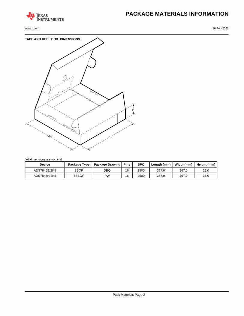
TAPE AND REEL INFORMATION
*All dimensions are nominal
Device PackageType
PackageDrawing
Pins SPQ ReelDiameter
(mm)
ReelWidth
W1 (mm)
A0(mm)
B0(mm)
K0(mm)
P1(mm)
W(mm)
Pin1Quadrant
ADS7846E/2K5 SSOP DBQ 16 2500 330.0 12.4 6.4 5.2 2.1 8.0 12.0 Q1
ADS7846N/2K5 TSSOP PW 16 2500 330.0 12.4 6.9 5.6 1.6 8.0 12.0 Q1
PACKAGE MATERIALS INFORMATION
www.ti.com 16-Feb-2022
Pack Materials-Page 1
*All dimensions are nominal
Device Package Type Package Drawing Pins SPQ Length (mm) Width (mm) Height (mm)
ADS7846E/2K5 SSOP DBQ 16 2500 367.0 367.0 35.0
ADS7846N/2K5 TSSOP PW 16 2500 367.0 367.0 35.0
PACKAGE MATERIALS INFORMATION
www.ti.com 16-Feb-2022
Pack Materials-Page 2
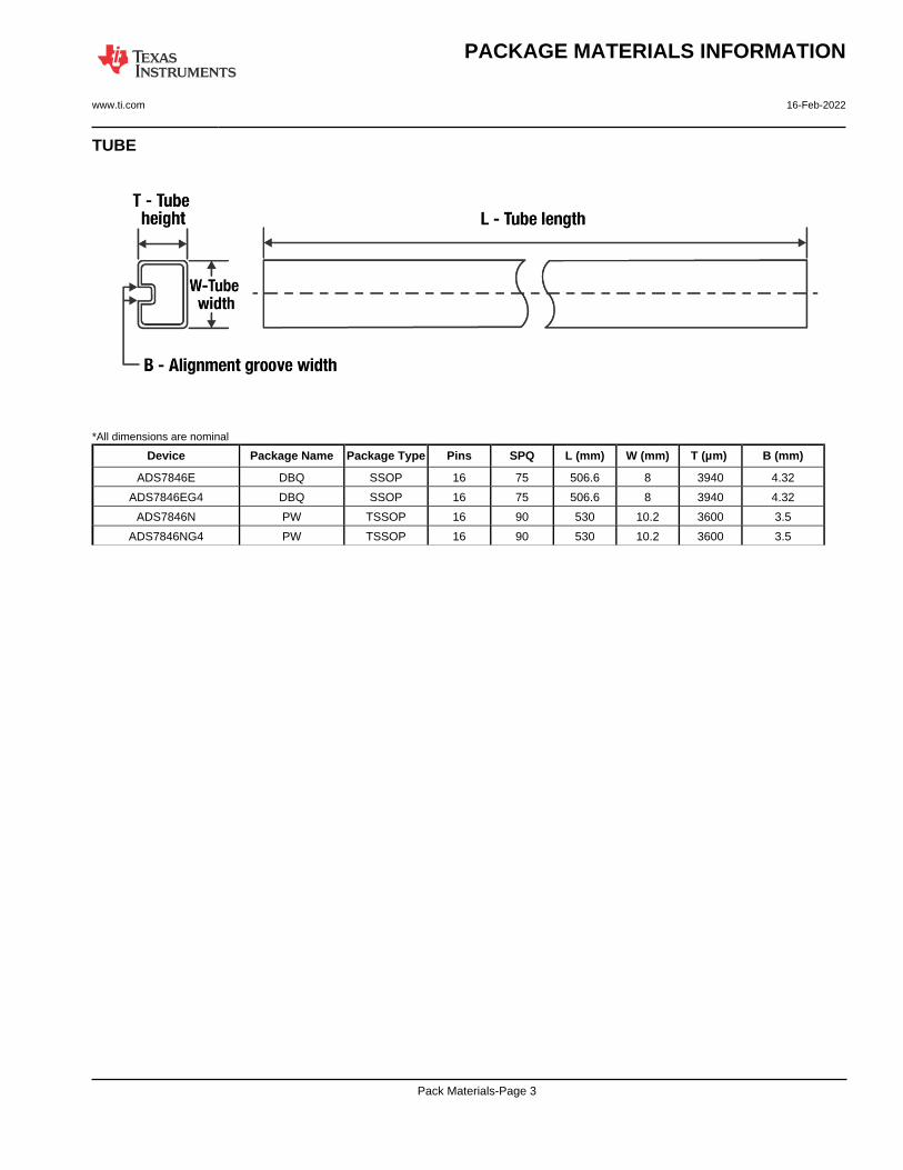
TUBE
*All dimensions are nominal
Device Package Name Package Type Pins SPQ L (mm) W (mm) T (µm) B (mm)
ADS7846E DBQ SSOP 16 75 506.6 8 3940 4.32
ADS7846EG4 DBQ SSOP 16 75 506.6 8 3940 4.32
ADS7846N PW TSSOP 16 90 530 10.2 3600 3.5
ADS7846NG4 PW TSSOP 16 90 530 10.2 3600 3.5
PACKAGE MATERIALS INFORMATION
www.ti.com 16-Feb-2022
Pack Materials-Page 3
www.ti.com
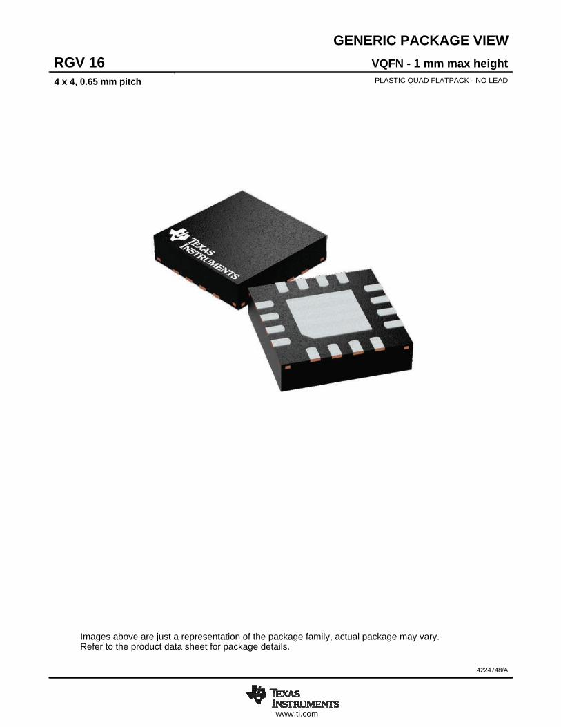
GENERIC PACKAGE VIEW
Images above are just a representation of the package family, actual package may vary.Refer to the product data sheet for package details.
VQFN - 1 mm max heightRGV 16PLASTIC QUAD FLATPACK - NO LEAD4 x 4, 0.65 mm pitch
4224748/A


www.ti.com
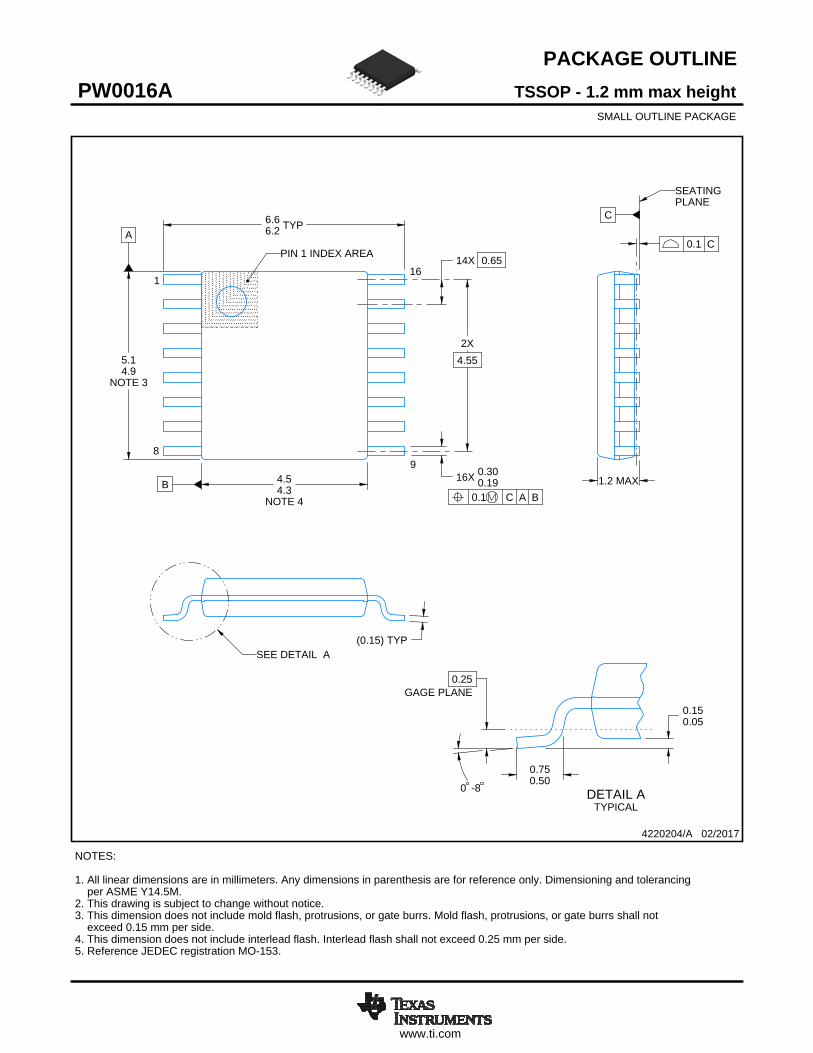
PACKAGE OUTLINE
C
14X 0.65
2X4.55
16X 0.300.19
TYP6.66.2
1.2 MAX
0.150.05
0.25GAGE PLANE
-80
BNOTE 4
4.54.3
A
NOTE 3
5.14.9
0.750.50
(0.15) TYP
TSSOP - 1.2 mm max heightPW0016ASMALL OUTLINE PACKAGE
4220204/A 02/2017
1
89
16
0.1 C A B
PIN 1 INDEX AREA
SEE DETAIL A
0.1 C
NOTES: 1. All linear dimensions are in millimeters. Any dimensions in parenthesis are for reference only. Dimensioning and tolerancing per ASME Y14.5M. 2. This drawing is subject to change without notice. 3. This dimension does not include mold flash, protrusions, or gate burrs. Mold flash, protrusions, or gate burrs shall not exceed 0.15 mm per side. 4. This dimension does not include interlead flash. Interlead flash shall not exceed 0.25 mm per side.5. Reference JEDEC registration MO-153.
SEATINGPLANE
A 20DETAIL ATYPICAL
SCALE 2.500
www.ti.com
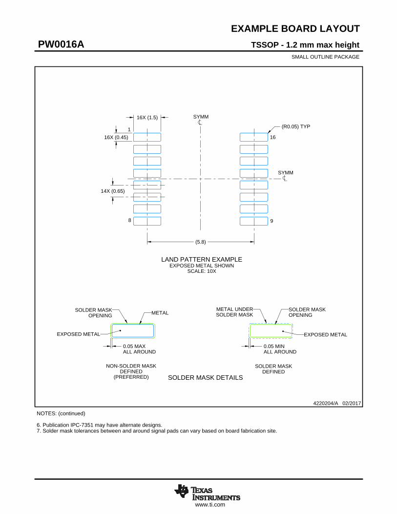
EXAMPLE BOARD LAYOUT
0.05 MAXALL AROUND
0.05 MINALL AROUND
16X (1.5)
16X (0.45)
14X (0.65)
(5.8)
(R0.05) TYP
TSSOP - 1.2 mm max heightPW0016ASMALL OUTLINE PACKAGE
4220204/A 02/2017
NOTES: (continued) 6. Publication IPC-7351 may have alternate designs. 7. Solder mask tolerances between and around signal pads can vary based on board fabrication site.
LAND PATTERN EXAMPLEEXPOSED METAL SHOWN
SCALE: 10X
SYMM
SYMM
1
8 9
16
15.000
METALSOLDER MASKOPENING
METAL UNDERSOLDER MASK
SOLDER MASKOPENING
EXPOSED METALEXPOSED METAL
SOLDER MASK DETAILS
NON-SOLDER MASKDEFINED
(PREFERRED)
SOLDER MASKDEFINED
www.ti.com
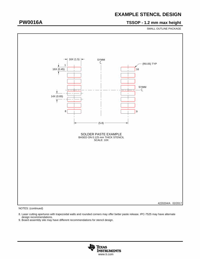
EXAMPLE STENCIL DESIGN
16X (1.5)
16X (0.45)
14X (0.65)
(5.8)
(R0.05) TYP
TSSOP - 1.2 mm max heightPW0016ASMALL OUTLINE PACKAGE
4220204/A 02/2017
NOTES: (continued) 8. Laser cutting apertures with trapezoidal walls and rounded corners may offer better paste release. IPC-7525 may have alternate design recommendations. 9. Board assembly site may have different recommendations for stencil design.
SOLDER PASTE EXAMPLEBASED ON 0.125 mm THICK STENCIL
SCALE: 10X
SYMM
SYMM
1
8 9
16
www.ti.com
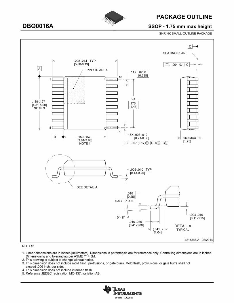
PACKAGE OUTLINE
C
TYP-.244.228-6.195.80[ ]
.069 MAX[1.75]
14X .0250[0.635]
16X -.012.008-0.300.21[ ]
2X.175[4.45]
TYP-.010.005-0.250.13[ ]
0 - 8-.010.004-0.250.11[ ]
(.041 )[1.04]
.010[0.25]
GAGE PLANE
-.035.016-0.880.41[ ]
A
NOTE 3
-.197.189-5.004.81[ ]
B
NOTE 4
-.157.150-3.983.81[ ]
SSOP - 1.75 mm max heightDBQ0016ASHRINK SMALL-OUTLINE PACKAGE
4214846/A 03/2014
NOTES: 1. Linear dimensions are in inches [millimeters]. Dimensions in parenthesis are for reference only. Controlling dimensions are in inches. Dimensioning and tolerancing per ASME Y14.5M. 2. This drawing is subject to change without notice. 3. This dimension does not include mold flash, protrusions, or gate burrs. Mold flash, protrusions, or gate burrs shall not exceed .006 inch, per side. 4. This dimension does not include interlead flash.5. Reference JEDEC registration MO-137, variation AB.
116
.007 [0.17] C A B
98
PIN 1 ID AREA
SEATING PLANE
.004 [0.1] C
SEE DETAIL A
DETAIL ATYPICAL
SCALE 2.800

www.ti.com
EXAMPLE BOARD LAYOUT
.002 MAX[0.05]ALL AROUND
.002 MIN[0.05]ALL AROUND
(.213)[5.4]
14X (.0250 )[0.635]
16X (.063)[1.6]
16X (.016 )[0.41]
SSOP - 1.75 mm max heightDBQ0016ASHRINK SMALL-OUTLINE PACKAGE
4214846/A 03/2014
NOTES: (continued) 6. Publication IPC-7351 may have alternate designs. 7. Solder mask tolerances between and around signal pads can vary based on board fabrication site.
METALSOLDER MASKOPENING
NON SOLDER MASKDEFINED
SOLDER MASK DETAILS
OPENINGSOLDER MASK METAL
SOLDER MASKDEFINED
LAND PATTERN EXAMPLESCALE:8X
SYMM
1
8 9
16
SEEDETAILS

www.ti.com
EXAMPLE STENCIL DESIGN
16X (.063)[1.6]
16X (.016 )[0.41]
14X (.0250 )[0.635]
(.213)[5.4]
SSOP - 1.75 mm max heightDBQ0016ASHRINK SMALL-OUTLINE PACKAGE
4214846/A 03/2014
NOTES: (continued) 8. Laser cutting apertures with trapezoidal walls and rounded corners may offer better paste release. IPC-7525 may have alternate design recommendations. 9. Board assembly site may have different recommendations for stencil design.
SOLDER PASTE EXAMPLEBASED ON .005 INCH [0.127 MM] THICK STENCIL
SCALE:8X
SYMM
SYMM
1
8 9
16

IMPORTANT NOTICE AND DISCLAIMERTI PROVIDES TECHNICAL AND RELIABILITY DATA (INCLUDING DATA SHEETS), DESIGN RESOURCES (INCLUDING REFERENCE DESIGNS), APPLICATION OR OTHER DESIGN ADVICE, WEB TOOLS, SAFETY INFORMATION, AND OTHER RESOURCES “AS IS” AND WITH ALL FAULTS, AND DISCLAIMS ALL WARRANTIES, EXPRESS AND IMPLIED, INCLUDING WITHOUT LIMITATION ANY IMPLIED WARRANTIES OF MERCHANTABILITY, FITNESS FOR A PARTICULAR PURPOSE OR NON-INFRINGEMENT OF THIRD PARTY INTELLECTUAL PROPERTY RIGHTS.These resources are intended for skilled developers designing with TI products. You are solely responsible for (1) selecting the appropriate TI products for your application, (2) designing, validating and testing your application, and (3) ensuring your application meets applicable standards, and any other safety, security, regulatory or other requirements.These resources are subject to change without notice. TI grants you permission to use these resources only for development of an application that uses the TI products described in the resource. Other reproduction and display of these resources is prohibited. No license is granted to any other TI intellectual property right or to any third party intellectual property right. TI disclaims responsibility for, and you will fully indemnify TI and its representatives against, any claims, damages, costs, losses, and liabilities arising out of your use of these resources.TI’s products are provided subject to TI’s Terms of Sale or other applicable terms available either on ti.com or provided in conjunction with such TI products. TI’s provision of these resources does not expand or otherwise alter TI’s applicable warranties or warranty disclaimers for TI products.TI objects to and rejects any additional or different terms you may have proposed. IMPORTANT NOTICE
Mailing Address: Texas Instruments, Post Office Box 655303, Dallas, Texas 75265Copyright © 2022, Texas Instruments Incorporated
Related Documents


