DATA SHEET Product specification Supersedes data of 2002 Jan 16 2003 Jan 30 INTEGRATED CIRCUITS PCF2119X LCD controllers/drivers

Welcome message from author
This document is posted to help you gain knowledge. Please leave a comment to let me know what you think about it! Share it to your friends and learn new things together.
Transcript
DATA SHEET
Product specificationSupersedes data of 2002 Jan 16
2003 Jan 30
INTEGRATED CIRCUITS
PCF2119XLCD controllers/drivers
2003 Jan 30 2
Philips Semiconductors Product specification
LCD controllers/drivers PCF2119X
CONTENTS
1 FEATURES
1.1 Note
2 APPLICATIONS
3 GENERAL DESCRIPTION
4 ORDERING INFORMATION
5 BLOCK DIAGRAM
6 PAD INFORMATION
6.1 Pad functions
7 FUNCTIONAL DESCRIPTION
7.1 LCD supply voltage generator7.2 Programming ranges7.3 LCD bias voltage generator7.4 Oscillator7.5 External clock7.6 Power-on reset7.7 Power-down mode7.8 Registers7.9 Busy flag7.10 Address Counter (AC)7.11 Display Data RAM (DDRAM)7.12 Character Generator ROM (CGROM)7.13 Character Generator RAM (CGRAM)7.14 Cursor control circuit7.15 Timing generator7.16 LCD row and column drivers7.17 Reset function
8 INSTRUCTIONS
8.1 Clear display8.2 Return home8.3 Entry mode set8.4 Display control (and partial power-down mode)8.5 Cursor or display shift8.6 Function set8.7 Set CGRAM address8.8 Set DDRAM address8.9 Read busy flag and read address8.10 Write data to CGRAM or DDRAM8.11 Read data from CGRAM or DDRAM
9 EXTENDED FUNCTION SETINSTRUCTIONS AND FEATURES
9.1 New instructions9.2 Icon control9.3 IM9.4 IB9.5 Normal/icon mode operation9.6 Direct mode9.7 Voltage multiplier control9.8 Screen configuration9.9 Display configuration9.10 TC1 and TC29.11 Set VLCD9.12 Reducing current consumption
10 INTERFACES TO MPU
10.1 Parallel interface10.2 I2C-bus interface
11 LIMITING VALUES
12 HANDLING
13 DC CHARACTERISTICS
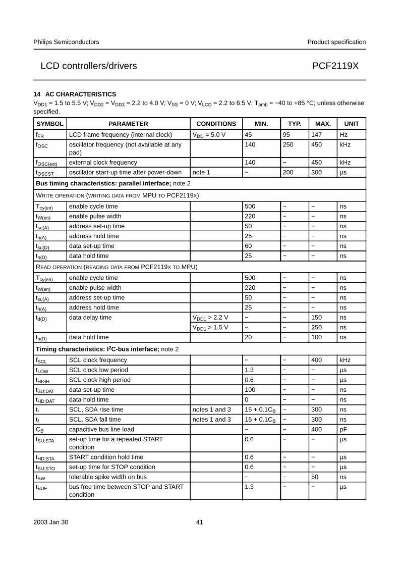
14 AC CHARACTERISTICS
15 TIMING CHARACTERISTICS
16 APPLICATION INFORMATION
16.1 General information16.2 Charge pump characteristics16.3 8-bit operation, 1-line display using external
reset16.4 4-bit operation, 1-line display using external
reset16.5 8-bit operation, 2-line display16.6 I2C-bus operation, 1-line display
17 DEVICE PROTECTION DIAGRAMS
18 BONDING PAD LOCATIONS
19 DATA SHEET STATUS
20 DEFINITIONS
21 DISCLAIMERS
22 PURCHASE OF PHILIPS I2C COMPONENTS
2003 Jan 30 3
Philips Semiconductors Product specification
LCD controllers/drivers PCF2119X
1 FEATURES
• Single-chip LCD controller/driver
• 2-line display of up to 16 characters + 160 icons, or1-line display of up to 32 characters + 160 icons
• 5 × 7 character format plus cursor; 5 × 8 for kana(Japanese) and user defined symbols
• Icon mode: reduced current consumption whiledisplaying icons only
• Icon blink function
• On-chip:
– Configurable 4 (3 and 2) times voltage multipliergenerating LCD supply voltage, independent of VDD,programmable by instruction (external supply alsopossible)
– Temperature compensation of on-chip generatedVLCD: −0.16 to −0.24 %/K (programmable byinstruction)
– Generation of intermediate LCD bias voltages
– Oscillator requires no external components (externalclock also possible).
• Display Data RAM: 80 characters
• Character Generator ROM: 240, 5 × 8 characters
• Character Generator RAM: 16, 5 × 8 characters;4 characters used to drive 160 icons, 8 characters usedif icon blink feature is used in application
• 4 or 8-bit parallel bus and 2-wire I2C-bus interface
• CMOS compatible
• 18 row and 80 column outputs
• Multiplex rates 1 : 18 (for normal operation), 1 : 9 (forsingle line operation) and 1 : 2 (for icon only mode)
• Uses common 11 code instruction set (extended)
• Logic supply voltage range, VDD1 − VSS = 1.5 to 5.5 V(chip may be driven with two battery cells)
• Display supply voltage range, VLCD − VSS = 2.2 to 6.5 V
• HVgen supply voltage range, VDD2 − VSS = 2.2 to 4 Vand VDD3 − VSS = 2.2 to 4 V
• Direct mode to save current consumption for icon modeand Mux 1 : 9 (depending on VDD2 value and LCD liquidproperties)
• Very low current consumption (20 to 200 µA):
– Icon mode: <25 µA
– Power-down mode: <2 µA.
1.1 Note
Icon mode is used to save current. When only icons aredisplayed, a much lower operating voltage VLCD can beused and the switching frequency of the LCD outputs isreduced. In most applications it is possible to use VDD asVLCD.
2 APPLICATIONS
• Telecom equipment
• Portable instruments
• Point-of-sale terminals.
3 GENERAL DESCRIPTION
The PCF2119x is a low power CMOS LCD controller anddriver, designed to drive a dot matrix LCD display of 2-lineby 16 or 1-line by 32 characters with 5 × 8 dot format. Allnecessary functions for the display are provided in a singlechip, including on-chip generation of LCD bias voltages,resulting in a minimum of external components and lowersystem current consumption. The PCF2119x interfaces tomost microcontrollers via a 4 or 8-bit bus or via the 2-wireI2C-bus. The chip contains a character generator anddisplays alphanumeric and kana (Japanese) characters.The letter ‘x’ in PCF2119x characterizes the built-incharacter set. Various character sets can be manufacturedon request.
2003 Jan 30 4
Philips Semiconductors Product specification
LCD controllers/drivers PCF2119X
4 ORDERING INFORMATION
TYPE NUMBERPACKAGE
NAME DESCRIPTION VERSION
PCF2119AU/2 − chip with bumps in tray 2PCF2119DU/2 − chip with bumps in tray 2PCF2119FU/2 − chip with bumps in tray 2PCF2119RU/2 − chip with bumps in tray 2PCF2119SU/2 − chip with bumps in tray 2PCF2119VU/2 − chip with bumps in tray 2
2003 Jan 30 5
Philips Semiconductors Product specification
LCD controllers/drivers PCF2119X
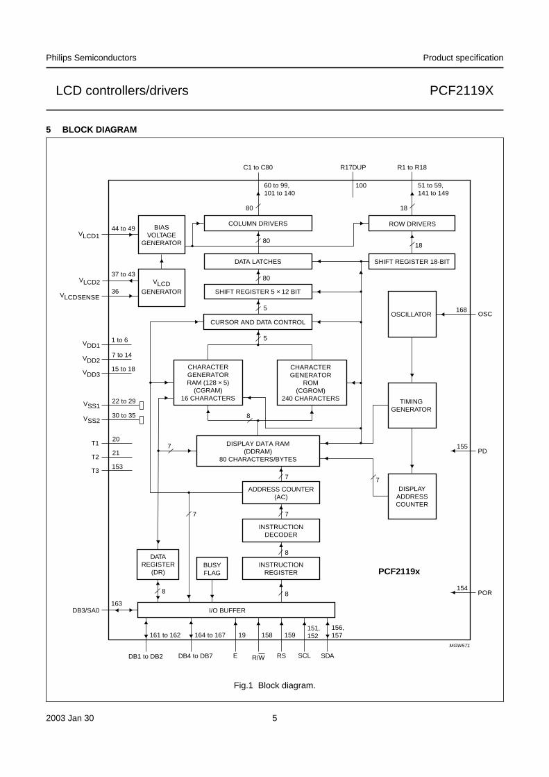
5 BLOCK DIAGRAM
handbook, full pagewidth
MGW571
CURSOR AND DATA CONTROL
SHIFT REGISTER 5 × 12 BIT
DATA LATCHES
COLUMN DRIVERS
80
5
80
CHARACTERGENERATORRAM (128 × 5)
(CGRAM)16 CHARACTERS
CHARACTERGENERATOR
ROM(CGROM)
240 CHARACTERS
DISPLAY DATA RAM(DDRAM)
80 CHARACTERS/BYTES
ADDRESS COUNTER(AC)
INSTRUCTIONDECODER
INSTRUCTIONREGISTER
ROW DRIVERS
SHIFT REGISTER 18-BIT
BIASVOLTAGE
GENERATOR
VLCDGENERATOR
BUSYFLAG
DATAREGISTER
(DR)
I/O BUFFER
OSCILLATOR
TIMINGGENERATOR
DISPLAYADDRESSCOUNTER
VDD1
VLCD2
VSS1
T1
VLCD144 to 49
VLCDSENSE36
37 to 43
22 to 29
20
T221
T3153
163
1 to 6
VDD27 to 14
VDD315 to 18
C1 to C80 R17DUP R1 to R18
OSC
PD
PCF2119x
DB1 to DB2
DB3/SA0
DB4 to DB7 E R/W RS SCL SDA
18
18
80
5
168
100
155
POR154
7 7
7
8
77
8
88
161 to 162
60 to 99,101 to 140
51 to 59,141 to 149
164 to 167156,157
151,15215915819
VSS230 to 35
Fig.1 Block diagram.
2003 Jan 30 6
Philips Semiconductors Product specification
LCD controllers/drivers PCF2119X
6 PAD INFORMATION
The identification of each pad and its location is given in Chapter 18.
6.1 Pad functions
Table 1 Pad function description
Note
1. When the I2C-bus is used, the parallel interface pad E must be at logic 0. In the I2C-bus read mode DB7 to DB4 andDB2 to DB0 should be connected to VDD1 or left open-circuit.
a) When the parallel bus is used, pads SCL and SDA must be connected to VSS1 or VDD1; they must not be leftopen-circuit.
b) If the 4-bit interface is used without reading out from the PCF2119x (i.e. R/W is set permanently to logic 0), theunused ports DB0 to DB4 can either be set to VSS1 or VDD1 instead of leaving them open-circuit.
SYMBOL DESCRIPTION
VDD1 Logic supply voltage.VDD2, VDD3 High voltage generator supply voltages (always put VDD2 = VDD3).VSS1 This is the ground pad for all except the high voltage generator.VSS2 This is the ground pad for the high voltage generator.VLCD1 This input is used for the generation of the LCD bias levels.VLCD2 This is the VLCD output pad if VLCD is generated internally then pad VLCD2 must be connected to VLCD1.
The pad must be left open-circuit when VLCD is generated externally.VLCDSENSE This input (VLCD) is used for the voltage multiplier’s regulation circuitry. This pad must be connected to
VLCD2 when using internal LCD supply and to VLCD1 and VLCD2 when using external LCD supply.E The data bus clock input is set HIGH to signal the start of a read or write operation; data is clocked in
or out of the chip on the negative edge of the clock; note 1.T1 to T3 These are three test pads. T1 and T2 must be connected to VSS1; T3 is left open-circuit and is not user
accessible.R1 to R18;R17DUP
LCD row driver outputs R1 to R18; these pads output the row select waveforms to the display;R17 and R18 drive the icons. R17 has two pads R17 and R17DUP.
C1 to C80 LCD column driver outputs C1 to C80.SCL I2C-bus serial clock input; note 1.POR External power-on reset input.PD PD selects the chip power-down mode; for normal operation PD = 0.SDA I2C-bus serial data input/output; note 1.R/W This is the read/write input. R/W selects either the read (R/W = 1) or write (R/W = 0) operation. This
pad has an internal pull-up resistor.RS The RS input selects the register to be accessed for read and write. RS = 0, selects the instruction
register for write and the busy flag and address counter for read. RS = 1, selects the data register forboth read and write. This pad has an internal pull-up resistor.
DB0 to DB7 The 8-bit bidirectional data bus (3-state) transfers data between the system controller and thePCF2119x. DB7 may be used as the busy flag, signalling that internal operations are not yetcompleted. In 4-bit operations the 4 higher order lines DB7 to DB4 are used; DB3 to DB0 must be leftopen-circuit. Data bus line DB3 has an alternative function (SA0), when selected this is the I2C-busaddress pad. Each data line has its own internal pull-up resistor; note 1.
OSC Oscillator or external clock input. When the on-chip oscillator is used this pad must be connected toVDD1.
2003 Jan 30 7
Philips Semiconductors Product specification
LCD controllers/drivers PCF2119X
7 FUNCTIONAL DESCRIPTION
7.1 LCD supply voltage generator
The LCD supply voltage may be generated on-chip. Thevoltage generator is controlled by two internal 6-bitregisters: VA and VB. The nominal LCD operating voltageat room temperature is given by the relationship:
7.2 Programming ranges
Programmed value: 1 to 63. Voltage: 1.90 to 6.86 V.Tref = 27 °C.
Values producing more than 6.5 V at operatingtemperature are not allowed. Operation above thisvoltage may damage the device. When programming theoperating voltage the VLCD temperature coefficient mustbe taken into account.
Values below 2.2 V are below the specified operatingrange of the chip and are therefore not allowed.
Value 0 for VA and VB switches the generator off(i.e. VA = 0 in character mode, VB = 0 in icon mode).
Usually register VA is programmed with the voltage forcharacter mode and register VB with the voltage for iconmode.
When VLCD is generated on-chip the VLCD pads should bedecoupled to VSS with a suitable capacitor. The generatedVLCD is independent of VDD and is temperaturecompensated.
When the generator and the direct mode are switched offan external voltage may be supplied at connected padsVLCD1. VLCD1 may be higher or lower than VDD.
During direct mode (program DM register bit) the internalvoltage generator is turned off and the VLCD output voltageis directly connected to VDD2. This reduces the currentconsumption during icon mode and Mux 1 : 9 (dependingon the VDD2 value and the LCD liquid properties).
The LCD supply voltage generator ensures that, as long asVDD is in the valid range (2.2 to 4 V), the required peakvoltage VOP = 6.5 V can be generated at any time.
7.3 LCD bias voltage generator
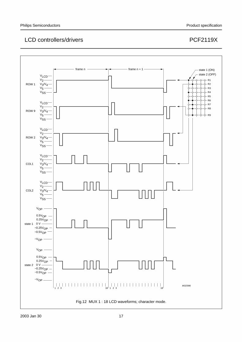
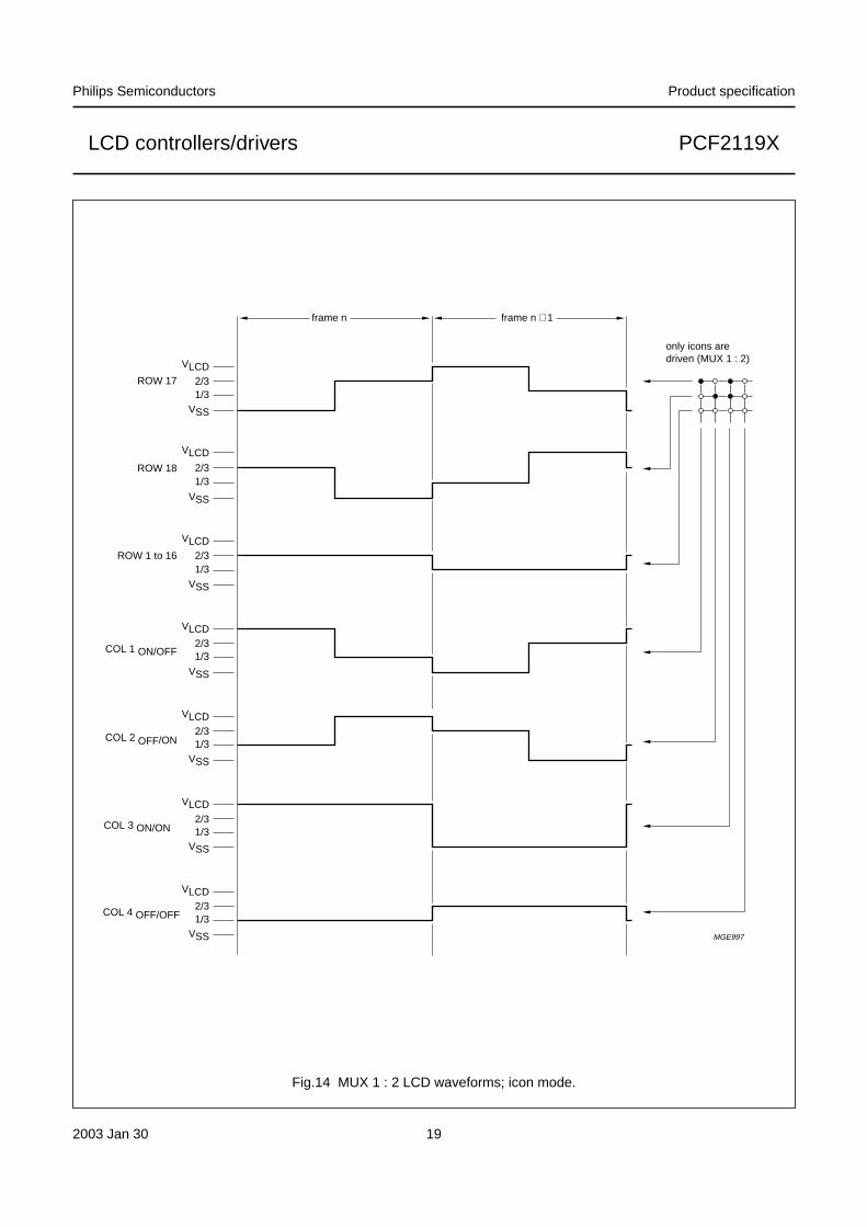
The intermediate bias voltages for the LCD display arealso generated on-chip. This removes the need for anexternal resistive bias chain and significantly reduces thesystem current consumption. The optimum value of VLCDdepends on the multiplex rate, the LCD threshold voltage(Vth) and the number of bias levels. Using a 5-level biasscheme for 1 : 18 maximum rate allows VLCD < 5 V formost LCD liquids. The intermediate bias levels for thedifferent multiplex rates are shown in Table 2. These biaslevels are automatically set to the given values whenswitching to the corresponding multiplex rate.
VOP(nom) integer value of register 0.08×( ) 1.82+=
Table 2 Bias levels as a function of multiplex rate
Note
1. The values in the above table are given relative to Vop − Vss, e.g. 3/4 means 3/4 × (Vop − Vss).
MULTIPLEXRATE
NUMBEROF LEVELS
V1 V2 V3 V4 V5 V6
1 : 18 5 Vop 3/4(1) 1/2 1/2 1/4 Vss
1 : 9 5 Vop 3/4 1/2 1/2 1/4 Vss
1 : 2 4 Vop 2/3 2/3 1/3 1/3 Vss
2003 Jan 30 8
Philips Semiconductors Product specification
LCD controllers/drivers PCF2119X
7.4 Oscillator
The on-chip oscillator provides the clock signal for thedisplay system. No external components are required andthe OSC pad must be connected to VDD.
7.5 External clock
If an external clock is to be used this is input at the OSCpad. The resulting display frame frequency is given by:
Only in the power-down state is the clock allowed to bestopped (OSC connected to VSS), otherwise the LCD isfrozen in a DC state.
7.6 Power-on reset
The PCF2119x must be reset externally. This is an internalsynchronous reset that requires 3 OSC cycles to beexecuted after release of the external reset signal. If noexternal reset is performed, the chip might start-up in anunwanted state. The external reset is active HIGH.
7.7 Power-down mode
The chip can be put into power-down mode by applying anexternal active HIGH level to the PD pad. In power-downmode all static currents are switched off (no internaloscillator, no bias level generation and all LCD outputs areinternally connected to VSS).
During power-down, information in the RAMs and the chipstate are preserved. Instruction execution duringpower-down is possible when pad OSC is externallyclocked.
7.8 Registers
The PCF2119x has two 8-bit registers, an InstructionRegister (IR) and a Data Register (DR). The RegisterSelect signal (RS) determines which register will beaccessed. The instruction register stores instruction codessuch as ‘display clear’ and ‘cursor shift’, and addressinformation for the Display Data RAM (DDRAM) andCharacter Generator RAM (CGRAM).
The instruction register can be written to but not read fromby the system controller. The data register temporarilystores data to be read from the DDRAM and CGRAM.When reading, data from the DDRAM or CGRAMcorresponding to the address in the instruction register iswritten to the data register prior to being read by the ‘readdata’ instruction.
7.9 Busy flag
The busy flag indicates the internal status of thePCF2119x. A logic 1 indicates that the chip is busy andfurther instructions will not be accepted. The busy flag isoutput to pad DB7 when RS = 0 and R/W = 1. Instructionsshould only be written after checking that the busy flag isat logic 0 or waiting for the required number of cycles.
7.10 Address Counter (AC)
The address counter assigns addresses to the DDRAMand CGRAM for reading and writing and is set by thecommands ‘set CGRAM address’ and ‘set DDRAMaddress’. After a read/write operation the address counteris automatically incremented or decremented by 1. Theaddress counter contents are output to the bus(DB6 to DB0) when RS = 0 and R/W = 1.
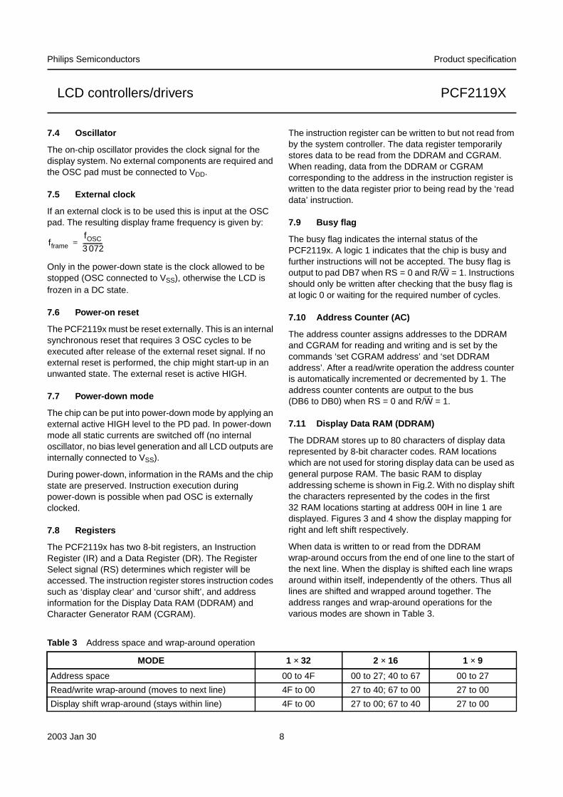
7.11 Display Data RAM (DDRAM)
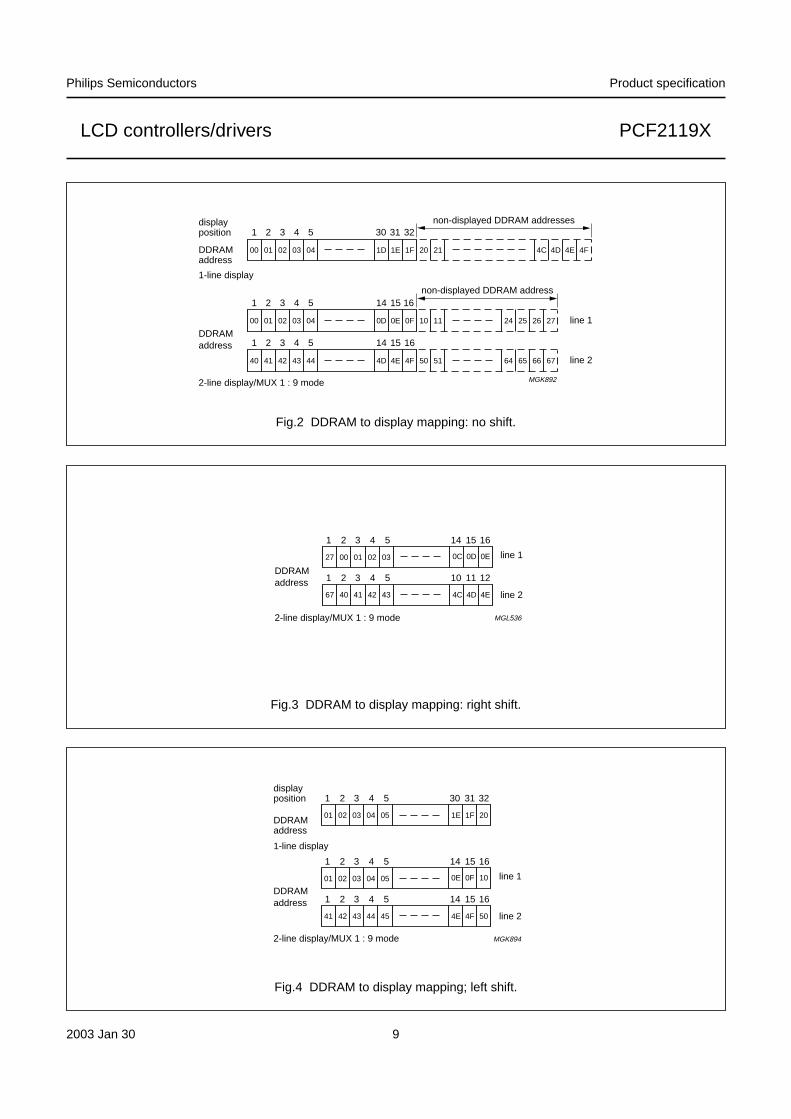
The DDRAM stores up to 80 characters of display datarepresented by 8-bit character codes. RAM locationswhich are not used for storing display data can be used asgeneral purpose RAM. The basic RAM to displayaddressing scheme is shown in Fig.2. With no display shiftthe characters represented by the codes in the first32 RAM locations starting at address 00H in line 1 aredisplayed. Figures 3 and 4 show the display mapping forright and left shift respectively.
When data is written to or read from the DDRAMwrap-around occurs from the end of one line to the start ofthe next line. When the display is shifted each line wrapsaround within itself, independently of the others. Thus alllines are shifted and wrapped around together. Theaddress ranges and wrap-around operations for thevarious modes are shown in Table 3.
fframe
fOSC
3 072-------------=
Table 3 Address space and wrap-around operation
MODE 1 × 32 2 × 16 1 × 9
Address space 00 to 4F 00 to 27; 40 to 67 00 to 27
Read/write wrap-around (moves to next line) 4F to 00 27 to 40; 67 to 00 27 to 00
Display shift wrap-around (stays within line) 4F to 00 27 to 00; 67 to 40 27 to 00
2003 Jan 30 9
Philips Semiconductors Product specification
LCD controllers/drivers PCF2119X
Fig.2 DDRAM to display mapping: no shift.
handbook, full pagewidth
00 01 02 03 04 1D 1E 1F 20 21 4C 4D 4E 4F
non-displayed DDRAM addresses
64 65 66 6740 41 42 43 44 4D 4E 4F 50 51
00 01 02 03 04 0D 0E 0F 10 11 24 25 26 27
non-displayed DDRAM address
line 1
line 2
MGK892
DDRAMaddress
2-line display/MUX 1 : 9 mode
1 2 3 4 5 30 31 32
1 2 3 4 5 14 15 16
1 2 3 4 5 14 15 16
displayposition
DDRAMaddress
1-line display
Fig.3 DDRAM to display mapping: right shift.
handbook, halfpage
MGL536
27 00 01 02 03
67 40 41 42 43
0C 0D 0E
4C 4D 4E
DDRAMaddress
line 1
line 2
2-line display/MUX 1 : 9 mode
1 2 3 4 5 14 15 16
1 2 3 4 5 10 11 12
Fig.4 DDRAM to display mapping; left shift.
handbook, halfpage
01 04 05
41 42 43 44 45
0E 0F 10
4E 4F 50
DDRAMaddress
line 1
line 2
2-line display/MUX 1 : 9 mode
1 2 3 4 5 30 31 32
1 2 3 4 5 14 15 16
1 2 3 4 5 14 15 16
01 04 05
02 03
02 03 1E 1F 20
displayposition
DDRAMaddress
1-line display
MGK894
2003 Jan 30 10
Philips Semiconductors Product specification
LCD controllers/drivers PCF2119X
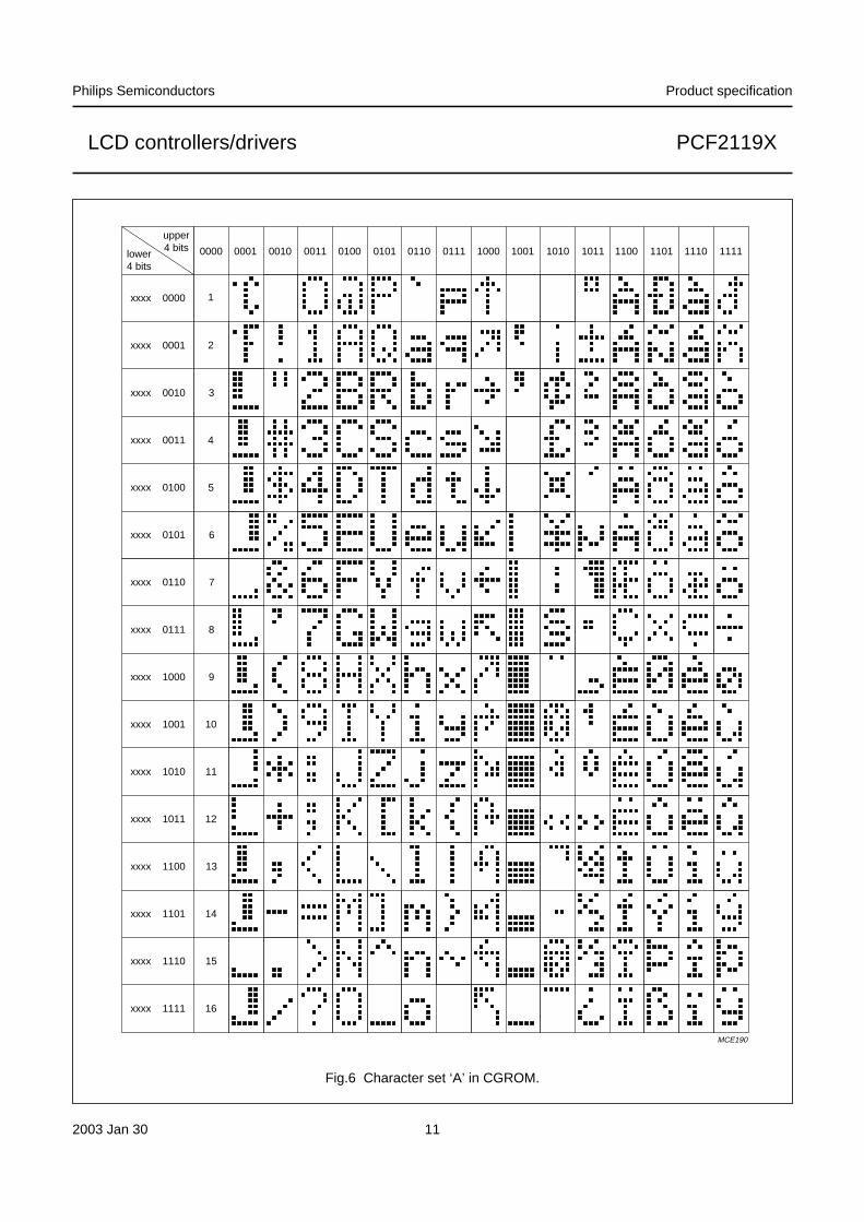
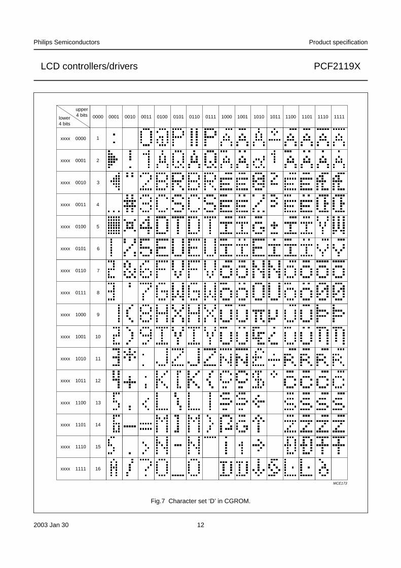
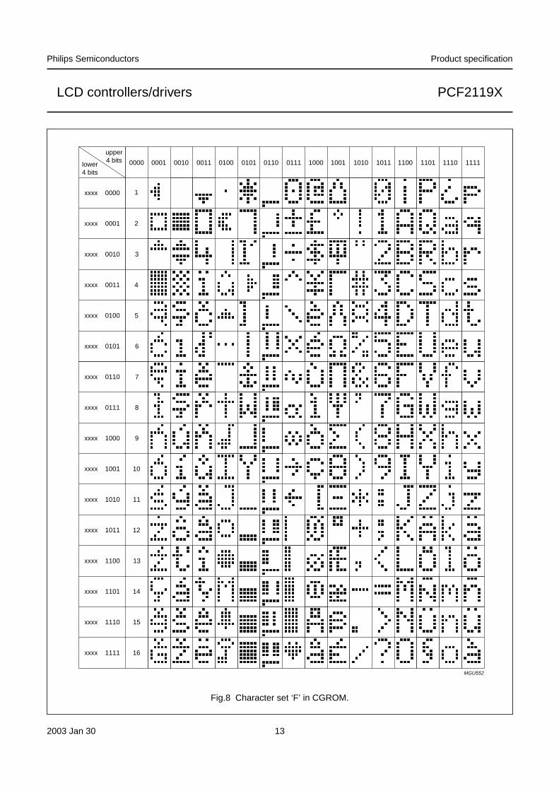
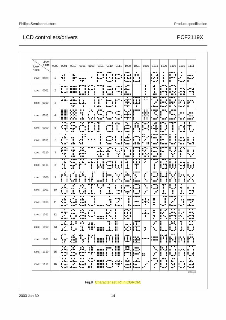
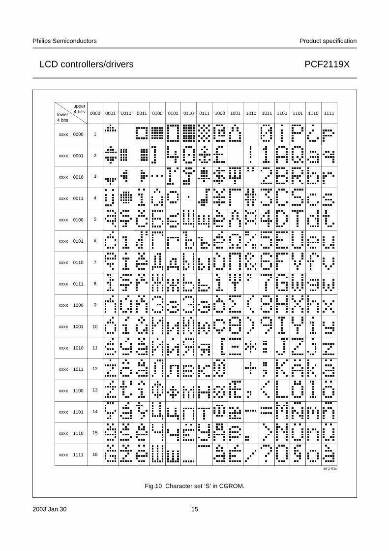
7.12 Character Generator ROM (CGROM)
The Character Generator ROM generates 240 characterpatterns in a 5 × 8 dot format from 8-bit character codes.Figures 6 to 10 shows the character sets that are currentlyimplemented.
7.13 Character Generator RAM (CGRAM)
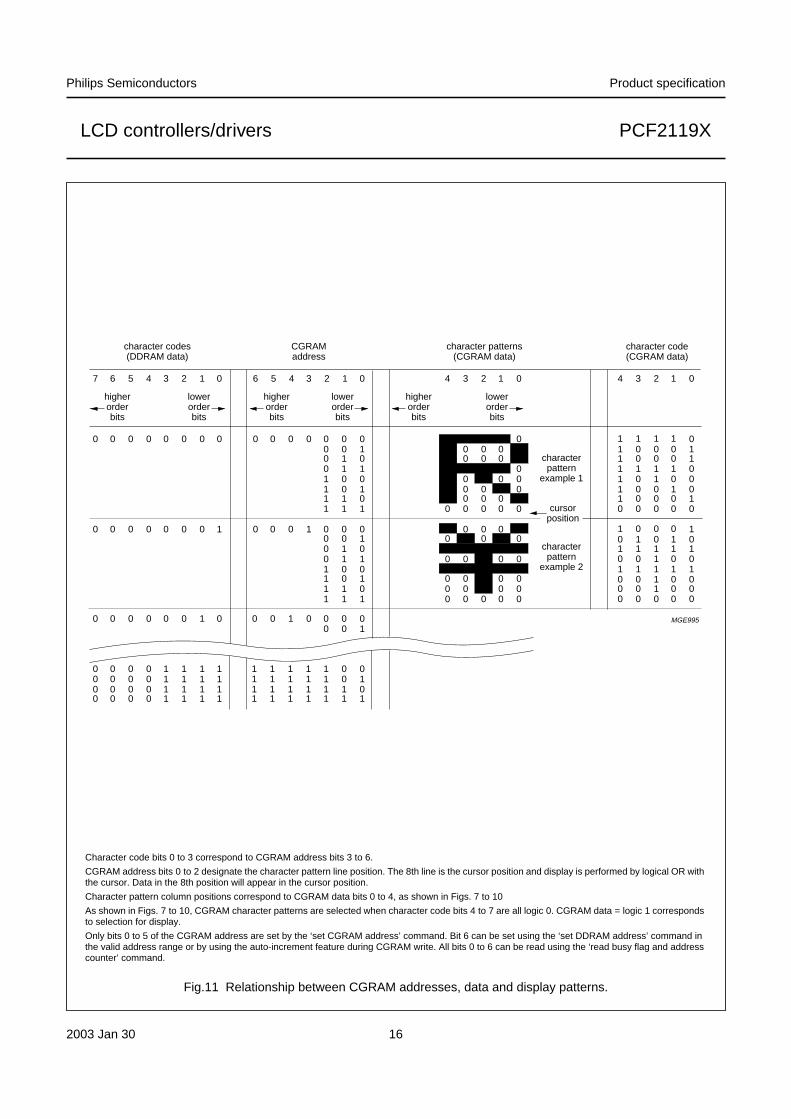
Up to 16 user defined characters may be stored in theCharacter Generator RAM. Some CGRAM characters(see Fig.19) are also used to drive icons (6 if icons blinkand both icon rows are used in the application; 3 if no blinkbut both icon rows are used in the application; 0 if no iconsare driven by the icon rows). The CGROM and CGRAMuse a common address space, of which the first column isreserved for the CGRAM (see Fig.6 to Fig.10). Figure 11shows the addressing principle for the CGRAM.
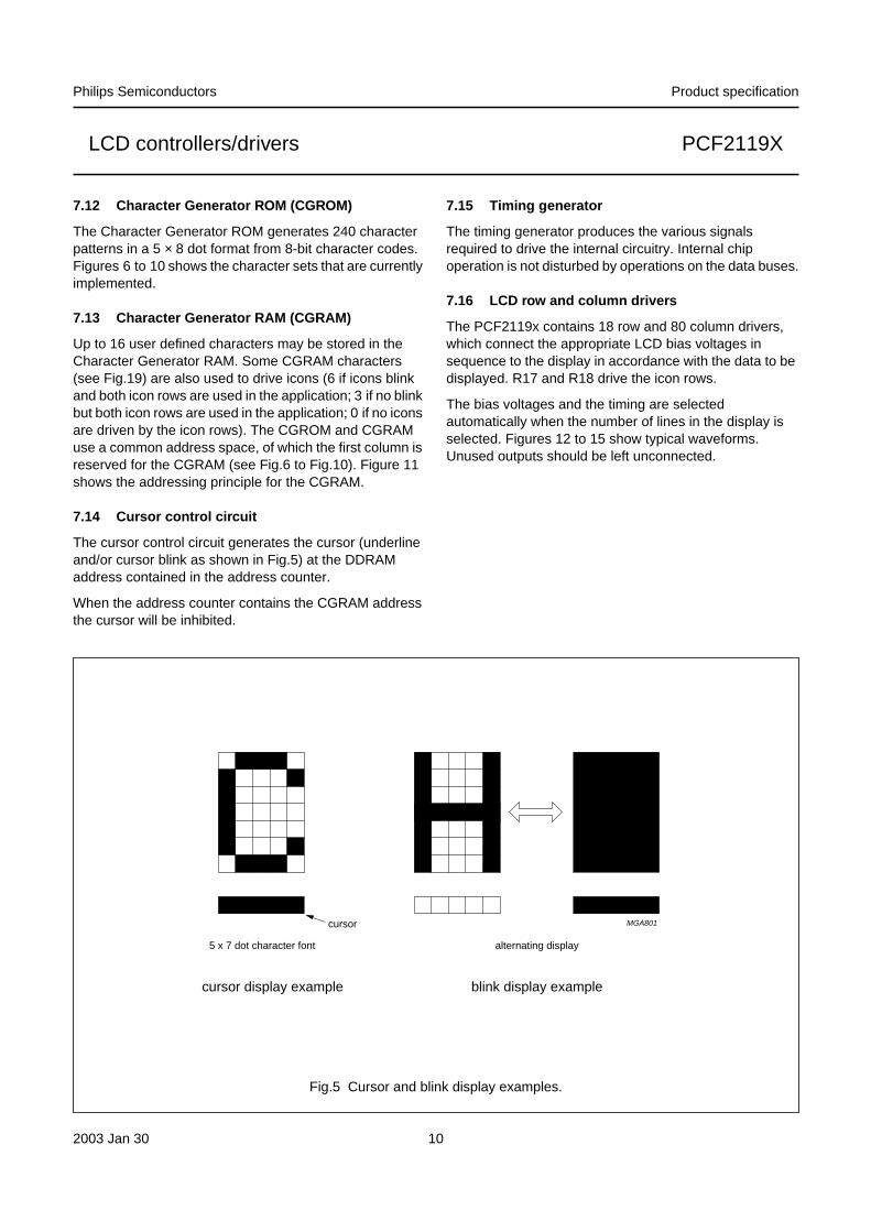
7.14 Cursor control circuit
The cursor control circuit generates the cursor (underlineand/or cursor blink as shown in Fig.5) at the DDRAMaddress contained in the address counter.
When the address counter contains the CGRAM addressthe cursor will be inhibited.
7.15 Timing generator
The timing generator produces the various signalsrequired to drive the internal circuitry. Internal chipoperation is not disturbed by operations on the data buses.
7.16 LCD row and column drivers
The PCF2119x contains 18 row and 80 column drivers,which connect the appropriate LCD bias voltages insequence to the display in accordance with the data to bedisplayed. R17 and R18 drive the icon rows.
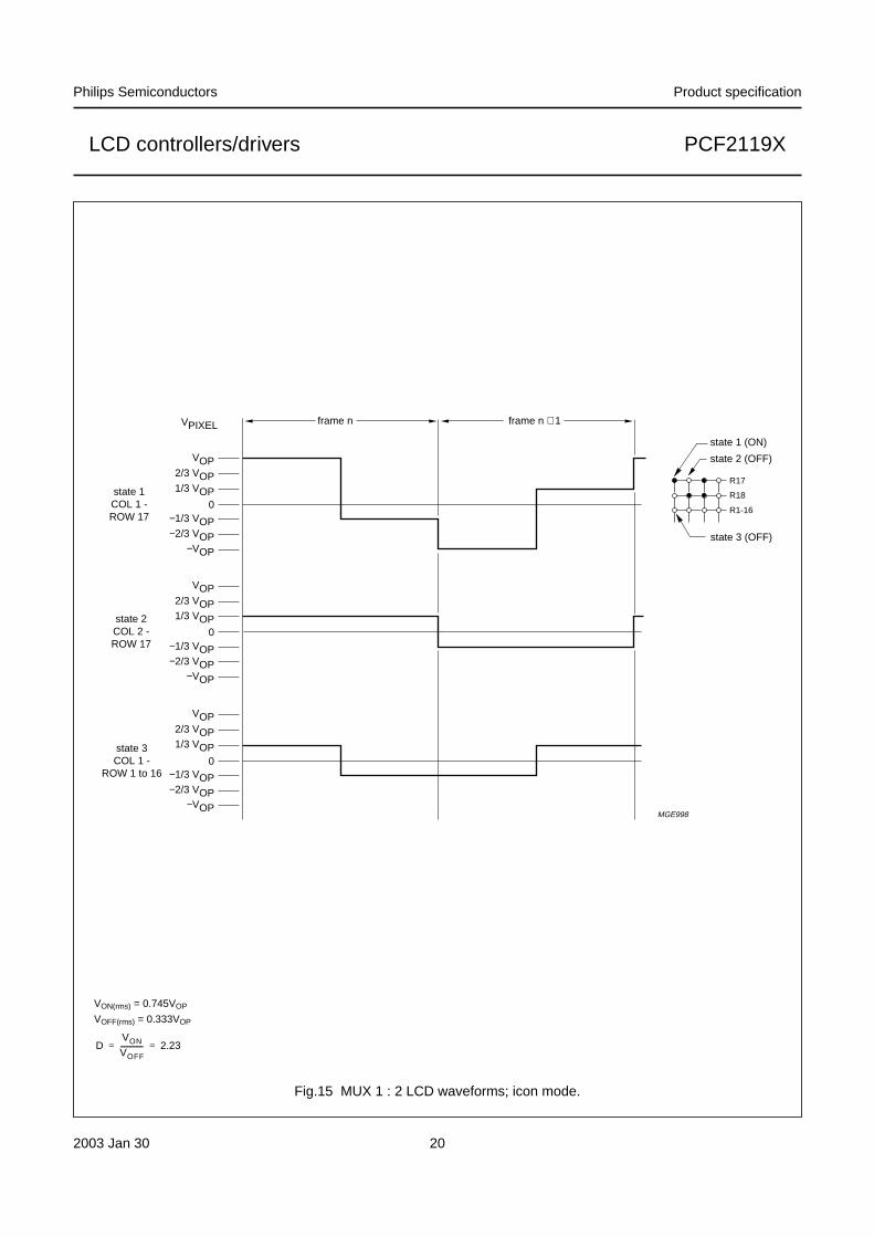
The bias voltages and the timing are selectedautomatically when the number of lines in the display isselected. Figures 12 to 15 show typical waveforms.Unused outputs should be left unconnected.
Fig.5 Cursor and blink display examples.
MGA801cursor
5 x 7 dot character font alternating display
cursor display example blink display example
2003 Jan 30 11
Philips Semiconductors Product specification
LCD controllers/drivers PCF2119X
handbook, full pagewidth
MCE190
xxxx 1111 16
0001 0010 0011 0100 0101 0110 0111 1000 1001 1010 1011 1100 1101 1110 11110000
upper4 bits
lower4 bits
xxxx 0000
xxxx 0001
xxxx 0010
xxxx 0011
xxxx 0100
xxxx 0101
xxxx 0110
xxxx 0111
xxxx 1000
xxxx 1001
xxxx 1010
xxxx 1011
xxxx 1100
xxxx 1101
xxxx 1110 15
14
13
12
11
10
9
8
7
6
5
4
3
2
1
Fig.6 Character set ‘A’ in CGROM.
2003 Jan 30 12
Philips Semiconductors Product specification
LCD controllers/drivers PCF2119X
handbook, full pagewidth
MCE173
xxxx 1111 16
0001 0010 0011 0100 0101 0110 0111 1000 1001 1010 1011 1100 1101 1110 11110000
upper4 bits
lower4 bits
xxxx 0000
xxxx 0001
xxxx 0010
xxxx 0011
xxxx 0100
xxxx 0101
xxxx 0110
xxxx 0111
xxxx 1000
xxxx 1001
xxxx 1010
xxxx 1011
xxxx 1100
xxxx 1101
xxxx 1110 15
14
13
12
11
10
9
8
7
6
5
4
3
2
1
Fig.7 Character set ‘D’ in CGROM.
2003 Jan 30 13
Philips Semiconductors Product specification
LCD controllers/drivers PCF2119X
handbook, full pagewidth
MGU552
xxxx 1111 16
0001 0010 0011 0100 0101 0110 0111 1000 1001 1010 1011 1100 1101 1110 11110000
upper4 bits
lower4 bits
xxxx 0000
xxxx 0001
xxxx 0010
xxxx 0011
xxxx 0100
xxxx 0101
xxxx 0110
xxxx 0111
xxxx 1000
xxxx 1001
xxxx 1010
xxxx 1011
xxxx 1100
xxxx 1101
xxxx 1110 15
14
13
12
11
10
9
8
7
6
5
4
3
2
1
Fig.8 Character set ‘F’ in CGROM.
2003 Jan 30 14
Philips Semiconductors Product specification
LCD controllers/drivers PCF2119X
Fig.9 Character set ‘R’ in CGROM.
handbook, full pagewidth
MGL535
xxxx 1111 16
0001 0010 0011 0100 0101 0110 0111 1000 1001 1010 1011 1100 1101 1110 11110000
upper4 bits
lower4 bits
xxxx 0000
xxxx 0001
xxxx 0010
xxxx 0011
xxxx 0100
xxxx 0101
xxxx 0110
xxxx 0111
xxxx 1000
xxxx 1001
xxxx 1010
xxxx 1011
xxxx 1100
xxxx 1101
xxxx 1110 15
14
13
12
11
10
9
8
7
6
5
4
3
2
1
MarcoS
Character set ‘R’ in CGROM.
2003 Jan 30 15
Philips Semiconductors Product specification
LCD controllers/drivers PCF2119X
Fig.10 Character set ‘S’ in CGROM.
handbook, full pagewidth
MGL534
xxxx 1111
0001 0010 0011 0100 0101 0110 0111 1000 1001 1010 1011 1100 1101 1110 11110000
1
2
3
4
5
6
7
8
9
10
11
12
13
14
15
16
upper4 bits
lower4 bits
xxxx 0000
xxxx 0001
xxxx 0010
xxxx 0011
xxxx 0100
xxxx 0101
xxxx 0110
xxxx 0111
xxxx 1000
xxxx 1001
xxxx 1010
xxxx 1011
xxxx 1100
xxxx 1101
xxxx 1110
2003 Jan 30 16
Philips Semiconductors Product specification
LCD controllers/drivers PCF2119X
Fig.11 Relationship between CGRAM addresses, data and display patterns.
Character code bits 0 to 3 correspond to CGRAM address bits 3 to 6.
CGRAM address bits 0 to 2 designate the character pattern line position. The 8th line is the cursor position and display is performed by logical OR withthe cursor. Data in the 8th position will appear in the cursor position.
Character pattern column positions correspond to CGRAM data bits 0 to 4, as shown in Figs. 7 to 10
As shown in Figs. 7 to 10, CGRAM character patterns are selected when character code bits 4 to 7 are all logic 0. CGRAM data = logic 1 correspondsto selection for display.
Only bits 0 to 5 of the CGRAM address are set by the ‘set CGRAM address’ command. Bit 6 can be set using the ‘set DDRAM address’ command inthe valid address range or by using the auto-increment feature during CGRAM write. All bits 0 to 6 can be read using the ‘read busy flag and addresscounter’ command.
handbook, full pagewidth
MGE995
7 6 5 4 3 2 1 0 6 5 4 3 2 1 0 4 3 2 1 0
higherorderbits
lowerorderbits
lowerorderbits
higherorderbits
lowerorderbits
higherorderbits
0 0 0 0 0 0 0 0 0 0 0 0 0 0 0 00 0 1 0 0 00 1 0 0 0 00 1 1 01 0 0 0 0 01 0 1 0 0 01 1 0 0 0 01 1 1 0 0 0 0 0
0 0 0 0 0 00 0 1 0 0 00 1 0
0 0 0 00 1 11 0 01 0 1 0 0 0 01 1 0 0 0 0 01 1 1 0 0 0 0 0
0 0 1
0 0 0 0 0 0 0 1 0 0 0 1
0 0 0 0 0 0 1 0
0 0 0 0 1 1 1 10 0 0 0 1 1 1 10 0 0 0 1 1 1 10 0 0 0 1 1 1 1
0 10 0 0 0 0
1 0 01 0 11 1 01
1111
1111
1111
1111 1 1
character codes(DDRAM data)
CGRAMaddress
character patterns(CGRAM data)
4 3 2 1 0
00 0 01 1 1
0 0 00
0 01 00 0 010 0 0
11
10 0
11
11 1 11
111
0 0 0
11 0 10 0 0
1 1 10
1 11 10 1 000 1 0
01
00 0
01
10 1 00
100
0 0 0
character code(CGRAM data)
characterpattern
example 1
cursorposition
characterpattern
example 2
2003 Jan 30 17
Philips Semiconductors Product specification
LCD controllers/drivers PCF2119X
Fig.12 MUX 1 : 18 LCD waveforms; character mode.
handbook, full pagewidth
MGE996
state 1 (ON)
state 2 (OFF)
frame n + 1 frame n
1 2 3 18 1 2 3 18
ROW 1
VLCDV2V3/V4V5VSS
ROW 9
VLCDV2V3/V4V5VSS
ROW 2
VLCDV2V3/V4V5VSS
COL1
VLCDV2V3/V4V5VSS
COL2
VLCDV2V3/V4V5VSS
0 Vstate 1
VOP
0.5VOP0.25VOP
−0.25VOP−0.5VOP
−VOP
0 Vstate 2
VOP
0.5VOP0.25VOP
−0.25VOP−0.5VOP
−VOP
R1
R2
R3
R4
R5
R6
R7
R8
R9

2003 Jan 30 18
Philips Semiconductors Product specification
LCD controllers/drivers PCF2119X
Fig.13 MUX 1 : 9 LCD waveforms; character mode. R10 to 18 to be left open.
handbook, full pagewidth
MGK900
state 1 (ON)
state 2 (OFF)
frame n + 1 frame n
1 9 1 9
ROW 1
VLCDV2V3/V4V5VSS
ROW 2
VLCDV2V3/V4V5VSS
ROW 3
VLCDV2V3/V4V5VSS
COL1
VLCDV2V3/V4V5VSS
COL2
VLCDV2V3/V4V5VSS
0 Vstate 1
VOP
0.5VOP0.25VOP
−0.25VOP−0.5VOP
−VOP
0 Vstate 2
VOP
0.5VOP0.25VOP
−0.25VOP−0.5VOP
−VOP
R1
R2
R3
R4
R5
R6
R7
R8
R9
2003 Jan 30 19
Philips Semiconductors Product specification
LCD controllers/drivers PCF2119X
Fig.14 MUX 1 : 2 LCD waveforms; icon mode.
handbook, full pagewidth
MGE997
frame n + 1 frame n
VLCD2/31/3
VSS
VLCD
2/31/3
VSS
VLCD2/31/3
VSS
VLCD2/31/3
VSS
VLCD2/31/3
VSS
VLCD2/31/3
VSS
VLCD2/31/3
VSS
COL 4 OFF/OFF
COL 3 ON/ON
COL 2 OFF/ON
COL 1 ON/OFF
ROW 1 to 16
ROW 18
ROW 17
only icons aredriven (MUX 1 : 2)
2003 Jan 30 20
Philips Semiconductors Product specification
LCD controllers/drivers PCF2119X
Fig.15 MUX 1 : 2 LCD waveforms; icon mode.
VON(rms) = 0.745VOP
VOFF(rms) = 0.333VOP
DVON
VOFF------------- 2.23= =
handbook, full pagewidth
MGE998
frame n + 1 frame n
VOP2/3 VOP1/3 VOP
0−1/3 VOP−2/3 VOP
−VOP
VOP2/3 VOP1/3 VOP
0−1/3 VOP−2/3 VOP
−VOP
VOP2/3 VOP1/3 VOP
0−1/3 VOP−2/3 VOP
−VOP
state 3COL 1 -
ROW 1 to 16
state 2COL 2 -ROW 17
state 1COL 1 -ROW 17
state 3 (OFF)
R17
R18
R1-16
VPIXEL
state 1 (ON)
state 2 (OFF)
2003 Jan 30 21
Philips Semiconductors Product specification
LCD controllers/drivers PCF2119X
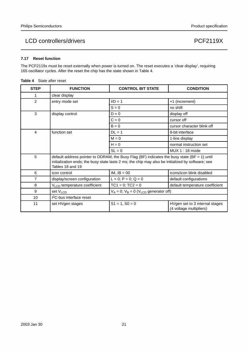
7.17 Reset function
The PCF2119x must be reset externally when power is turned on. The reset executes a ‘clear display’, requiring165 oscillator cycles. After the reset the chip has the state shown in Table 4.
Table 4 State after reset
STEP FUNCTION CONTROL BIT STATE CONDITION
1 clear display
2 entry mode set I/D = 1 +1 (increment)
S = 0 no shift
3 display control D = 0 display off
C = 0 cursor off
B = 0 cursor character blink off
4 function set DL = 1 8-bit interface
M = 0 1-line display
H = 0 normal instruction set
SL = 0 MUX 1 : 18 mode
5 default address pointer to DDRAM; the Busy Flag (BF) indicates the busy state (BF = 1) untilinitialization ends; the busy state lasts 2 ms; the chip may also be initialized by software; seeTables 18 and 19
6 icon control IM, IB = 00 icons/icon blink disabled
7 display/screen configuration L = 0; P = 0; Q = 0 default configurations
8 VLCD temperature coefficient TC1 = 0; TC2 = 0 default temperature coefficient
9 set VLCD VA = 0; VB = 0 (VLCD generator off)
10 I2C-bus interface reset
11 set HVgen stages S1 = 1, S0 = 0 HVgen set to 3 internal stages(4 voltage multipliers)

2003 Jan 30 22
Philips Semiconductors Product specification
LCD controllers/drivers PCF2119X
8 INSTRUCTIONS
Only two PCF2119x registers, the Instruction Register (IR)and the Data Register (DR) can be directly controlled bythe MPU. Before internal operation, control information isstored temporarily in these registers, to allow interfacing tovarious types of MPUs which operate at different speedsor to allow interface to peripheral control ICs. ThePCF2119x operation is controlled by the instructionsshown in Table 6 together with their execution time.Details are explained in subsequent sections.
Instructions are of 4 types, those that:
1. Designate PCF2119x functions such as displayformat, data length, etc.
2. Set internal RAM addresses
3. Perform data transfer with internal RAM
4. Others.
In normal use, category 3 instructions are used mostfrequently. However, automatic incrementing by 1(or decrementing by 1) of internal RAM addresses aftereach data write lessens the MPU program load. Thedisplay shift in particular can be performed concurrentlywith display data write, enabling the designer to developsystems in minimum time with maximum programmingefficiency.
During internal operation, no instructions other than the‘read busy flag’ and ‘read address’ instructions will beexecuted. Because the busy flag is set to a logic 1 while aninstruction is being executed, check to ensure it is a logic 0before sending the next instruction or wait for themaximum instruction execution time, as given in Table 6.An instruction sent while the busy flag is logic 1 will not beexecuted.
Table 5 Instruction set for I2C-bus commands
Note
1. R/W is set together with the slave address.
CONTROL BYTE COMMAND BYTE I 2C-BUS COMMANDS
Co RS 0 0 0 0 0 0 DB7 DB6 DB5 DB4 DB3 DB2 DB1 DB0 note 1
2003Jan
3023
Philips S
emiconductors
Product specification
LCD
controllers/driversP
CF
2119X
This text is here in white to force landscape pages to be rotated correctly when browsing through the pdf in the Acrobat reader.This text is here in_white to force landscape pages to be rotated correctly when browsing through the pdf in the Acrobat reader.This text is here inThis text is here inwhite to force landscape pages to be rotated correctly when browsing through the pdf in the Acrobat reader. white to force landscape pages to be ...
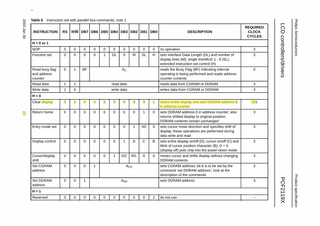
Table 6 Instruction set with parallel bus commands; note 1
INSTRUCTION RS R/W DB7 DB6 DB5 DB4 DB3 DB2 DB1 DB0 DESCRIPTIONREQUIRED
CLOCKCYCLES
H = 0 or 1
NOP 0 0 0 0 0 0 0 0 0 0 no operation 3
Function set 0 0 0 0 1 DL 0 M SL H sets interface Data Length (DL) and number ofdisplay lines (M); single line/MUX 1 : 9 (SL),extended instruction set control (H)
3
Read busy flagand addresscounter
0 1 BF AC reads the Busy Flag (BF) indicating internaloperating is being performed and reads addresscounter contents
0
Read data 1 1 read data reads data from CGRAM or DDRAM 3
Write data 1 0 write data writes data from CGRAM or DDRAM 3
H = 0
Clear display 0 0 0 0 0 0 0 0 0 1 clears entire display and sets DDRAM address 0in address counter
165
Return home 0 0 0 0 0 0 0 0 1 0 sets DDRAM address 0 in address counter; alsoreturns shifted display to original position;DDRAM contents remain unchanged
3
Entry mode set 0 0 0 0 0 0 0 1 I/D S sets cursor move direction and specifies shift ofdisplay; these operations are performed duringdata write and read
3
Display control 0 0 0 0 0 0 1 D C B sets entire display on/off (D), cursor on/off (C) andblink of cursor position character (B); D = 0(display off) puts chip into the power-down mode
3
Cursor/displayshift
0 0 0 0 0 1 S/C R/L 0 0 moves cursor and shifts display without changingDDRAM contents
3
Set CGRAMaddress
0 0 0 1 ACG sets CGRAM address; bit 6 is to be set by thecommand ‘set DDRAM address’; look at thedescription of the commands
3
Set DDRAMaddress
0 0 1 ADD sets DDRAM address 3
H = 1
Reserved 0 0 0 0 0 0 0 0 0 1 do not use −
MarcoS
23 display 0 0 0 0 0 0 0 0 0 1 clears entire display and sets DDRAM address 0 in address counter 165
2003Jan
3024
Philips S
emiconductors
Product specification
LCD
controllers/driversP
CF
2119X
This text is here in white to force landscape pages to be rotated correctly when browsing through the pdf in the Acrobat reader.This text is here in_white to force landscape pages to be rotated correctly when browsing through the pdf in the Acrobat reader.This text is here inThis text is here inwhite to force landscape pages to be rotated correctly when browsing through the pdf in the Acrobat reader. white to force landscape pages to be ...
Note
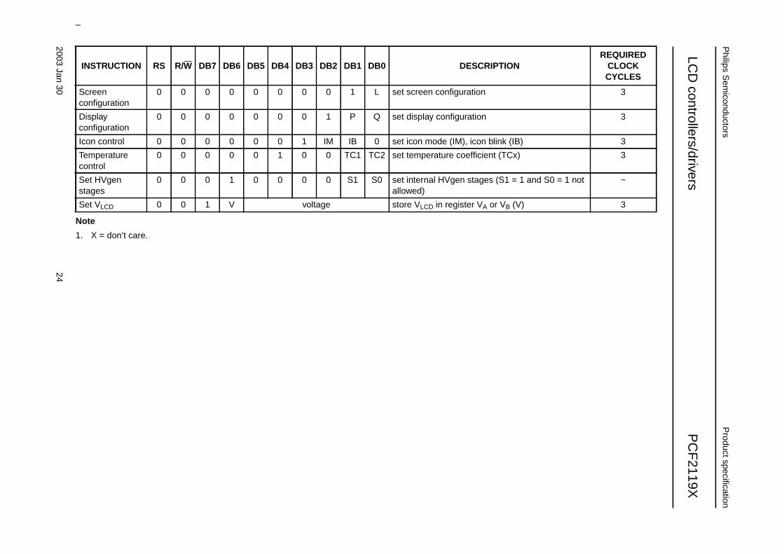
1. X = don’t care.
Screenconfiguration
0 0 0 0 0 0 0 0 1 L set screen configuration 3
Displayconfiguration
0 0 0 0 0 0 0 1 P Q set display configuration 3
Icon control 0 0 0 0 0 0 1 IM IB 0 set icon mode (IM), icon blink (IB) 3
Temperaturecontrol
0 0 0 0 0 1 0 0 TC1 TC2 set temperature coefficient (TCx) 3
Set HVgenstages
0 0 0 1 0 0 0 0 S1 S0 set internal HVgen stages (S1 = 1 and S0 = 1 notallowed)
−
Set VLCD 0 0 1 V voltage store VLCD in register VA or VB (V) 3
INSTRUCTION RS R/W DB7 DB6 DB5 DB4 DB3 DB2 DB1 DB0 DESCRIPTIONREQUIRED
CLOCKCYCLES

2003 Jan 30 25
Philips Semiconductors Product specification
LCD controllers/drivers PCF2119X
Table 7 Explanations of symbols used in Table 6
Table 8 Explanation of TC1 and TC2 used in Table 6
Note
1. For values of the temperature coefficients, see Chapter 13
BITSTATE
LOGIC 0 LOGIC 1
I/D decrement incrementS display freeze display shiftD display off display onC cursor off cursor onB cursor character blink off: character at cursor
position does not blinkcursor character blink on: character at cursorposition blinks
S/C cursor move display shiftR/L left shift right shiftDL 4 bits 8 bitsH use basic instruction set use extended instruction setL (no impact, ifM = 1 or SL = 1)
left/right screen: standard connection (as inPCF2114)
left/right screen: mirrored connection (as inPCF2116)
1st 16 characters of 32: columns are from1 to 80
1st 16 characters of 32: columns are from1 to 80
2nd 16 characters of 32: columns are from1 to 80
2nd 16 characters of 32: columns are from80 to 1
P column data: left to right (as in PCF2116);column data is displayed from 1 to 80
column data: right to left; column data isdisplayed from 80 to 1
Q row data top to bottom (as in PCF2116): row data bottom to top:row data is displayed from 1 to 16 and icon rowdata in 17 and 18
row data is displayed from 16 to 1 and icon rowdata in 18 and 17
in single line mode (SL = 1) row data isdisplayed from 1 to 8 and icon row data in 17
in single line mode (SL = 1) row data isdisplayed from 8 to 1 and icon row data in 17
IM character mode; full display icon mode; only icons displayedIB icon blink disabled icon blink enabledDM direct mode disable direct mode enableV set VA set VB
M (no impact, ifSL = 1)
1-line by 32 display 2-line by 16 display
SL MUX 1 : 18 (1 × 32 or 2 × 16 character display) MUX 1 : 9 (1 × 16 character display)C0 last control byte; see Table 5 another control byte follows after data/command
TC1 TC2 DESCRIPTION(1)
0 0 VLCD temperature coefficient 01 0 VLCD temperature coefficient 10 1 VLCD temperature coefficient 21 1 VLCD temperature coefficient 3
2003 Jan 30 26
Philips Semiconductors Product specification
LCD controllers/drivers PCF2119X
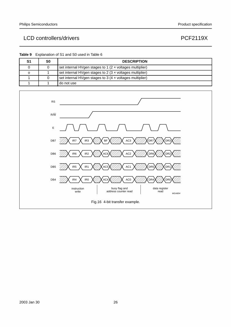
Table 9 Explanation of S1 and S0 used in Table 6
S1 S0 DESCRIPTION
0 0 set internal HVgen stages to 1 (2 × voltages multiplier)o 1 set internal HVgen stages to 2 (3 × voltages multiplier)1 0 set internal HVgen stages to 3 (4 × voltages multiplier)1 1 do not use
Fig.16 4-bit transfer example.
MGA804
RS
E
DB7
R/W
DB6
DB5
DB4
instructionwrite
busy flag andaddress counter read
data registerread
IR7 IR3 BF AC3 DR7 DR3
IR6 IR2 AC6 AC2 DR6 DR2
IR5 IR1 AC5 AC1 DR5 DR1
IR4 IR0 AC4 AC0 DR4 DR0
2003 Jan 30 27
Philips Semiconductors Product specification
LCD controllers/drivers PCF2119X
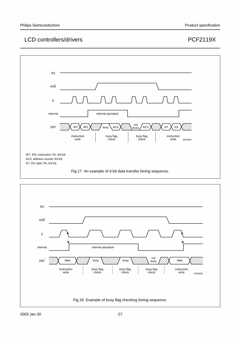
Fig.17 An example of 4-bit data transfer timing sequence.
IR7, IR3: instruction 7th, 3rd bit.
AC3: address counter 3rd bit.
D7, D3: data 7th, 3rd bit.
MGA805
RS
E
internal
DB7
R/W
internal operation
IR7 IR3 AC3 D7 D3not
busyAC3busy
instructionwrite
busy flagcheck
busy flagcheck
instructionwrite
Fig.18 Example of busy flag checking timing sequence.
MGA806
instructionwrite
busy flagcheck
busy flagcheck
busy flagcheck
instructionwrite
internal operation
RS
E
internal
DB7
R/W
data busy busynot
busy data
2003 Jan 30 28
Philips Semiconductors Product specification
LCD controllers/drivers PCF2119X
8.1 Clear display
‘Clear display’ writes character code 20H into all DDRAMaddresses (the character pattern for character code 20Hmust be a blank pattern), sets the DDRAM addresscounter to logic 0 and returns the display to its originalposition, if it was shifted. Thus, the display disappears andthe cursor or blink position goes to the left edge of thedisplay. Sets entry mode I/D = 1 (increment mode). S ofentry mode does not change.
The instruction ‘clear display’ requires extra executiontime. This may be allowed by checking the Busy Flag (BF)or by waiting until the 165 clock cycles have elapsed. Thelatter must be applied where no read-back options areforeseen, as in some Chip-On-Glass (COG) applications.
8.2 Return home
‘Return home’ sets the DDRAM address counter to logic 0and returns the display to its original position if it wasshifted. DDRAM contents do not change. The cursor orblink position goes to the left of the first display line.I/D and S of entry mode do not change.
8.3 Entry mode set
8.3.1 I/D
When I/D = 1 (0) the DDRAM or CGRAM addressincrements (decrements) by 1 when data is written into orread from the DDRAM or CGRAM. The cursor or blinkposition moves to the right when incremented and to theleft when decremented. The cursor underline and cursorcharacter blink are inhibited when the CGRAM isaccessed.
8.3.2 S
When S = 1, the entire display shifts either to the right(I/D = 0) or to the left (I/D = 1) during a DDRAM write. Thusit appears as if the cursor stands still and the displaymoves. The display does not shift when reading from theDDRAM, or when writing to or reading from the CGRAM.When S = 0, the display does not shift.
8.4 Display control (and partial power-down mode)
8.4.1 D
The display is on when D = 1 and off when D = 0. Displaydata in the DDRAM is not affected and can be displayedimmediately by setting D to a logic 1.
When the display is off (D = 0) the chip is in partialpower-down mode:
• The LCD outputs are connected to VSS
• The LCD generator and bias generator are turned off.
Three oscillator cycles are required after sending the‘display off’ instruction to ensure all outputs are at VSS,afterwards OSC can be stopped. If the oscillator is runningduring partial power-down mode (‘display off’) the chip canstill execute instructions. Even lower current consumptionis obtained by inhibiting the oscillator (OSC = VSS).
To ensure IDD <1 µA, the parallel bus pads DB7 to DB0should be connected to VDD; RS and R/W to VDD or leftopen-circuit and PD to VDD. Recovery from power-downmode: PD back to logic 0, if necessary OSC back to VDDand send a ‘display control’ instruction with D = 1.
8.4.2 C
The cursor is displayed when C = 1 and inhibited whenC = 0. Even if the cursor disappears, the display functionsI/D, etc. remain in operation during display data write. Thecursor is displayed using 5 dots in the 8th line (see Fig.5).
8.4.3 B
The character indicated by the cursor blinks when B = 1.The cursor character blink is displayed by switchingbetween display characters and all dots on with a period of
approximately 1 second, with
The cursor underline and the cursor character blink can beset to display simultaneously.
8.5 Cursor or display shift
‘Cursor/display shift’ moves the cursor position or thedisplay to the right or left without writing or reading displaydata. This function is used to correct a character or movethe cursor through the display. In 2-line displays, thecursor moves to the next line when it passes the lastposition (40) of the line.
When the displayed data is shifted repeatedly all lines shiftat the same time; displayed characters do not shift into thenext line.
The Address Counter (AC) content does not change if theonly action performed is shift display, but increments ordecrements with the ‘cursor shift’.
fblink
fOSC
52 224-----------------=
2003 Jan 30 29
Philips Semiconductors Product specification
LCD controllers/drivers PCF2119X
8.6 Function set
8.6.1 DL (PARALLEL MODE ONLY)
Sets interface data width. Data is sent or received in bytes(DB7 to DB0) when DL = 1 or in two nibbles (DB7 to DB4)when DL = 0. When 4-bit width is selected, data istransmitted in two cycles using the parallel bus. In a 4-bitapplication DB3 to DB0 should be left open-circuit (internalpull-ups). Hence in the first ‘function set’ instruction afterpower-on, M, SL and H are set to logic 1. A second‘function set’ must then be sent (2 nibbles) to set M,SL and H to their required values.
‘Function set’ from the I2C-bus interface sets the DL bit tologic 1.
8.6.2 M
Selects either 1-line by 32 display (M = 0) or 2-line by16 display (M = 1).
8.6.3 SL
Selects MUX 1 : 9, 1-line by 16 display (independent ofM and L). Only rows 1 to 8 and 17 are to be used. All otherrows must be left open-circuit. The DDRAM map is thesame as in the 2-line by 16 display mode, however, thesecond line is not displayable.
8.6.4 H
When H = 0 the chip can be programmed via the standard11 instruction codes used in the PCF2116 and other LCDcontrollers.
When H = 1 the extended range of instructions will beused. These are mainly for controlling the displayconfiguration and the icons.
8.7 Set CGRAM address
‘Set CGRAM address’ sets bits 5 to 0 of the CGRAMaddress ACG into the address counter (binary A5 to A0).Data can then be written to or read from the CGRAM.
Attention: the CGRAM address uses the same addressregister as the DDRAM address and consists of 7 bits(binary A6 to A0). With the ‘set CGRAM address’command, only bits 5 to 0 are set. Bit 6 can be set usingthe ‘set DDRAM address’ command first, or by using theauto-increment feature during CGRAM write. All bits 6 to 0can be read using the ‘read busy flag’ and ‘read address’command.
When writing to the lower part of the CGRAM, ensure thatbit 6 of the address is not set (e.g. by an earlier DDRAMwrite or read action).
8.8 Set DDRAM address
‘Set DDRAM address’ sets the DDRAM address ADD intothe address counter (binary A6 to A0). Data can then bewritten to or read from the DDRAM.
8.9 Read busy flag and read address
‘Read busy flag’ and ‘read address’ read the Busy Flag(BF) and Address Counter (AC). BF = 1 indicates that aninternal operation is in progress. The next instruction willnot be executed until BF = 0. It is recommended that theBF status is checked before the next write operation isexecuted.
At the same time, the value of the address counterexpressed in binary A6 to A0 is read out. The addresscounter is used by both CGRAM and DDRAM, and itsvalue is determined by the previous instruction.
8.10 Write data to CGRAM or DDRAM
‘Write data’ writes binary 8-bit data D7 to D0 to theCGRAM or the DDRAM.
Whether the CGRAM or DDRAM is to be written into isdetermined by the previous ‘set CGRAM address’ or ‘setDDRAM address’ command. After writing, the addressautomatically increments or decrements by 1, inaccordance with the entry mode. Only bits D4 to D0 ofCGRAM data are valid, bits D7 to D5 are ‘don’t care’.
8.11 Read data from CGRAM or DDRAM
‘Read data’ reads binary 8-bit data D7 to D0 from theCGRAM or DDRAM.
The most recent ‘set address’ command determineswhether the CGRAM or DDRAM is to be read.
The ‘read data’ instruction gates the content of the DataRegister (DR) to the bus while E is HIGH. After E goesLOW again, internal operation increments (or decrements)the AC and stores RAM data corresponding to the new ACinto the DR.
There are only three instructions that update the dataregister:
• ‘set CGRAM address’
• ‘set DDRAM address’
• ‘read data’ from CGRAM or DDRAM.
Other instructions (e.g. ‘write data’, ‘cursor/display shift’,‘clear display’ and ‘return home’) do not modify the dataregister content.
2003 Jan 30 30
Philips Semiconductors Product specification
LCD controllers/drivers PCF2119X
9 EXTENDED FUNCTION SET INSTRUCTIONS ANDFEATURES
9.1 New instructions
H = 1, sets the chip into alternate instruction set mode.
9.2 Icon control
The PCF2119x can drive up to 160 icons. See Fig.19 forCGRAM to icon mapping.
9.3 IM
When IM = 0, the chip is in character mode. In thecharacter mode characters and icons are driven(MUX 1 : 18). The VLCD generator, if used, produces theVLCD voltage programmed in register VA.
When IM = 1, the chip is in icon mode. In the icon modeonly the icons are driven (MUX 1 : 2) and the VLCD voltagegenerator, if used, produces the VLCD voltage asprogrammed in register VB.
9.4 IB
Icon blink control is independent of the cursor/characterblink function.
When IB = 0, icon blink is disabled. Icon data is stored inCGRAM character 0 to 3 (4 × 8 × 5 = 160 bits for160 icons).
When IB = 1, icon blink is enabled. In this case each iconis controlled by two bits. Blink consists of two half phases(corresponding to the cursor on and off phases called evenand odd phases hereafter).
Icon states for the even phase are stored in CGRAMcharacters 0 to 3 (4 × 8 × 5 = 160 bits for 160 icons).These bits also define the icon state when icon blink is notused.
Icon states for the odd phase are stored in CGRAMcharacter 4 to 7 (another 160 bits for the 160 icons). Whenicon blink is disabled CGRAM characters 4 to 6 may beused as normal CGRAM characters.
Table 10 Blink effect for icons and cursor character blink
PARAMETER EVEN PHASE ODD PHASE
Cursor character blink block (all on) normal (display character)
Icons state 1: CGRAM character 0 to 2 state 2: CGRAM character 4 to 6

2003 Jan 30 31
Philips Semiconductors Product specification
LCD controllers/drivers PCF2119X
Fig.19 CGRAM to icon mapping.
CGRAM data bit = logic 1 turns the icon on, data bit = logic 0 turns the icon off.
Data in character codes 0 to 3 define the icon state when icon blink is disabled or during the even phase when icon blink is enabled.
Data in character codes 4 to 7 define the icon state during the odd phase when icon blink is enabled (not used for icons when icon blink is disabled).
handbook, full pagewidth
MGK999
156-160 odd (blink) 18/76-80 0 0 0 0 0 1 1 1
icon view
0 1 1 1 1 1 1 0 0 1 1 0
1-5 odd (blink) 17/1-5 0 0 0 0 0 1 0 0 0 1 0 0 0 0 0 0 0 0 0 0
156-160 even 18/76-80 0 0 0 0 0 0 1 1 0 0 1 1 1 1 1 1 1 1 0 1
81-85 even 18/1-5 0 0 0 0 0 0 1 0 0 0 1 0 0 0 0 1 1 0 0 0
76-80 even 17/76-80 0 0 0 0 0 0 0 1 0 0 0 1 1 1 1 1 1 1 1 1
11-15 even 17/11-15 0 0 0 0 0 0 0 0 0 0 0 0 0 1 0 0 1 1 1 0
6-10 even 17/6-10 0 0 0 0 0 0 0 0 0 0 0 0 0 0 1 0 1 0 1 0
1-5 even 17/1-5 0 0 0 0 0 0 0 0 0 0 0 0 0 0 0 1 0 1 0 1
7 6 5 4 3 2 1 0
MSB LSB LSBMSB MSBLSB
6 5 4 3 2 1 0 4 3 2 1 0
icon no. phase ROW/COL character codes CGRAM address CGRAM data
handbook, full pagewidth COL 1 to 5
1 2 3 4 5
81 82 83 84 85
display:
ROW 17 –
ROW 18 –
block of 5 columns
COL 6 to 10
6 7 8 9 10
86 87 88 89 90
COL 76 to 80
76 77 78 79 80
156 157 158 159 160
MGL249
2003 Jan 30 32
Philips Semiconductors Product specification
LCD controllers/drivers PCF2119X
9.5 Normal/icon mode operation
9.6 Direct mode
When DM = 0, the chip is not in direct mode. Either theinternal voltage generator or an external voltage may beused to achieve the necessary VLCD value.
When DM = 1, the chip is in direct mode. The internalvoltage generator is turned off and the VLCD output isdirectly connected to the HVgen supply voltage VDD2.
The direct mode can be used to reduce the currentconsumption when the required VLCD output voltage isclose to the VDD2 supply voltage. This can be the case inicon mode or in Mux 1 : 9 (depending on LCD liquidproperties).
9.7 Voltage multiplier control
S[1:0]
A software configurable voltage multiplier is incorporatedand can be set via ‘Set HVgen stages’ command.
The voltage multiplier control can be used to reducecurrent consumption by disconnecting internal voltagemultiplier stages (depending on the required VLCD outputvoltage).
9.8 Screen configuration
L: default is L = 0.
L = 0: the two halves of a split screen are connected in astandard way i.e. column 1/81, 2/82 to 80/160.
L = 1: the two halves of a split screen are connected in amirrored way i.e. column 1/160, 2/159 to 80/81. Thisallows single layer PCB or glass layout.
9.9 Display configuration
P, Q: default is P, Q = 0.
P = 1: mirrors the column data.
Q = 1: mirrors the row data.
9.10 TC1 and TC2
Default is TC1 and TC2 = 0. This selects the defaulttemperature coefficient for the internally generated VLCD.TC1 and TC2 = 10, 01 and 11 selects alternativetemperature coefficients 1, 2 and 3 respectively.
9.11 Set VLCD
The VLCD value is programmed by instruction. Two on-chipregisters hold VLCD values for the character mode and theicon mode respectively (VA and VB). The generated VLCDvalue is independent of VDD, allowing battery operation ofthe chip.
VLCD programming:
1. Send ‘function set’ instruction with H = 1
2. Send ‘set VLCD’ instruction to write to voltage register:
a) DB7, DB6 = 10: DB5 to DB0 are VLCD of charactermode (VA)
b) DB7, DB6 = 11: DB5 to DB0 are VLCD of icon mode(VB)
c) DB5 to DB0 = 000000 switches VLCD generator off(when selected)
d) During ‘display off’ and power-down the VLCDgenerator is also disabled.
3. Send ‘function set’ instruction with H = 0 to resumenormal programming.
9.12 Reducing current consumption
Reducing current consumption can be achieved by one ofthe options given in Table 11.
When VLCD lies outside the VDD range and must begenerated, it is usually more efficient to use the on-chipgenerator than an external regulator.
Table 11 Reducing current consumption
Table 12 Use of the VA and VB registers
IM CONDITION VLCD
0 character mode generates VA
1 icon mode generates VB
ORIGINAL MODE ALTERNATIVE MODE
Character mode icon mode (control bit IM)
Display on display off (control bit D)
HV generator operating direct mode
Any mode power-down (PD pad)
MODE VA VB
Normal operation VLCD charactermode
VLCD icon mode
2003 Jan 30 33
Philips Semiconductors Product specification
LCD controllers/drivers PCF2119X
10 INTERFACES TO MPU
10.1 Parallel interface
The PCF2119x can send data in either two 4-bit operationsor one 8-bit operation and can thus interface to 4-bit or8-bit microcontrollers.
In 8-bit mode data is transferred as 8-bit bytes using the8 data lines DB7 to DB0. Three further control linesE, RS and R/W are required; see Section 6.1.
In 4-bit mode data is transferred in two cycles of 4 bitseach using pads DB7 to DB4 for the transaction. Thehigher order bits (corresponding to DB7 to DB4 in 8-bitmode) are sent in the first cycle and the lower order bits(DB3 to DB0 in 8-bit mode) in the second. Data transfer iscomplete after two 4-bit data transfers. It should be notedthat two cycles are also required for the busy flag check.4-bit operation is selected by instruction, see Figs 16 to 18for examples of bus protocol.
In 4-bit mode, pads DB3 to DB0 must be left open-circuit.They are pulled up to VDD internally.
10.2 I2C-bus interface
The I2C-bus is for bidirectional, two-line communicationbetween different ICs or modules. The two lines are theSerial Data line (SDA) and the Serial Clock Line (SCL).Both lines must be connected to a positive supply viapull-up resistors. Data transfer may be initiated only whenthe bus is not busy.
Each byte of eight bits is followed by an acknowledge bit.The acknowledge bit is a HIGH level signal put on the busby the transmitter during which time the master generatesan extra acknowledge related clock pulse. A slave receiverwhich is addressed must generate an acknowledge afterthe reception of each byte.
Also a master receiver must generate an acknowledgeafter the reception of each byte that has been clocked outof the slave transmitter.
The device that acknowledges must pull-down the SDAline during the acknowledge clock pulse, so that the SDAline is stable LOW during the HIGH period of theacknowledge related clock pulse (set-up and hold timesmust be taken into consideration).
A master receiver must signal an end of data to thetransmitter by not generating an acknowledge on the lastbyte that has been clocked out of the slave. In this eventthe transmitter must leave the data line HIGH to enable themaster to generate a STOP condition.
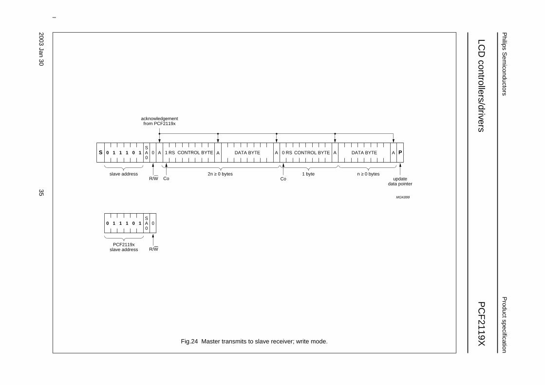
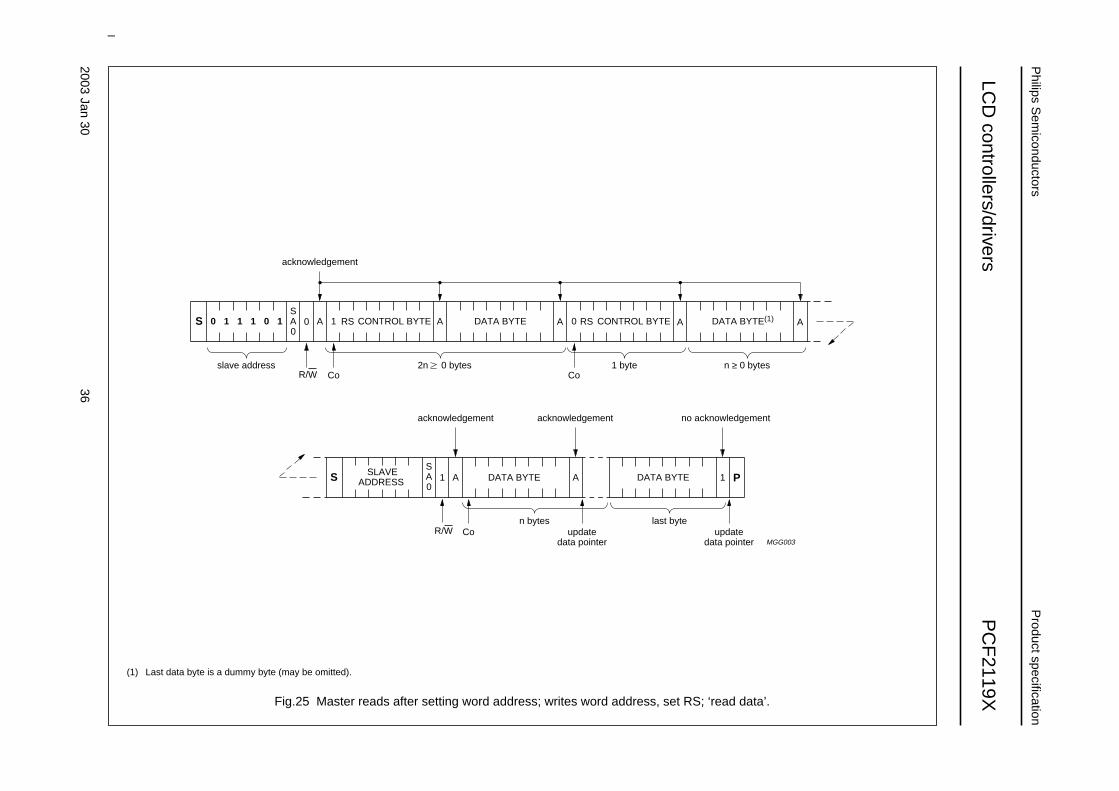
10.2.1 I2C-BUS PROTOCOL
Before any data is transmitted on the I2C-bus, the devicewhich should respond is addressed first. The addressing isalways carried out with the first byte transmitted after theSTART procedure. The I2C-bus configuration for thedifferent PCF2119x read and write cycles is shown inFigs 24 to 26. The slow down feature of the I2C-busprotocol (receiver holds SCL LOW during internaloperations) is not used in the PCF2119x.
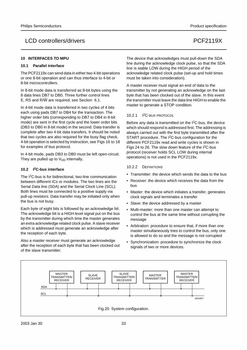
10.2.2 DEFINITIONS
• Transmitter: the device which sends the data to the bus
• Receiver: the device which receives the data from thebus
• Master: the device which initiates a transfer, generatesclock signals and terminates a transfer
• Slave: the device addressed by a master
• Multi-master: more than one master can attempt tocontrol the bus at the same time without corrupting themessage
• Arbitration: procedure to ensure that, if more than onemaster simultaneously tries to control the bus, only oneis allowed to do so and the message is not corrupted
• Synchronization: procedure to synchronize the clocksignals of two or more devices.
Fig.20 System configuration.
MGA807
SDA
SCL
MASTERTRANSMITTER/
RECEIVER
MASTERTRANSMITTER
SLAVETRANSMITTER/
RECEIVER
SLAVERECEIVER
MASTERTRANSMITTER/
RECEIVER
2003 Jan 30 34
Philips Semiconductors Product specification
LCD controllers/drivers PCF2119X
Fig.21 Bit transfer.
handbook, full pagewidth
MBC621
data linestable;
data valid
changeof dataallowed
SDA
SCL
Fig.22 Definition of START and STOP conditions.
handbook, full pagewidth
MBC622
SDA
SCLP
STOP condition
SDA
SCLS
START condition
handbook, full pagewidth
MBC602
S
STARTcondition
9821
clock pulse foracknowledgement
not acknowledge
acknowledge
DATA OUTPUTBY TRANSMITTER
DATA OUTPUTBY RECEIVER
SCL FROMMASTER
Fig.23 Acknowledgement on the I2C-bus.
2003Jan
3035
Philips S
emiconductors
Product specification
LCD
controllers/driversP
CF
2119X
This text is here in white to force landscape pages to be rotated correctly when browsing through the pdf in the Acrobat reader.This text is here in_white to force landscape pages to be rotated correctly when browsing through the pdf in the Acrobat reader.This text is here inThis text is here inwhite to force landscape pages to be rotated correctly when browsing through the pdf in the Acrobat reader. white to force landscape pages to be ...
handbook, full pagewidth
MGK899
SA0
S P0 1 1 1 0 1 0 A
slave address
CONTROL BYTE A1
Co
DATA BYTE A CONTROL BYTE A
R/W
0
Co updatedata pointer
1 byte n ≥ 0 bytes2n ≥ 0 bytes
DATA BYTE A
acknowledgementfrom PCF2119x
RS RS
SA0
0 1 1 1 0 1 0
PCF2119xslave address R/W
Fig.24 Master transmits to slave receiver; write mode.
2003Jan
3036
Philips S
emiconductors
Product specification
LCD
controllers/driversP
CF
2119X
This text is here in white to force landscape pages to be rotated correctly when browsing through the pdf in the Acrobat reader.This text is here in_white to force landscape pages to be rotated correctly when browsing through the pdf in the Acrobat reader.This text is here inThis text is here inwhite to force landscape pages to be rotated correctly when browsing through the pdf in the Acrobat reader. white to force landscape pages to be ...
handbook, full pagewidth
MGG003
SA0
S 0 1 1 1 0 1 0 A
slave address
CONTROL BYTE A1
Co
DATA BYTE A CONTROL BYTE A
R/W
0
Co
Co updatedata pointer
updatedata pointer
1 byte n ≥ 0 bytes
n bytes last byte
2n 0 bytes
DATA BYTE(1) A
acknowledgement
SA0
S 1 A DATA BYTE A 1 P SLAVEADDRESS DATA BYTE
acknowledgement acknowledgement no acknowledgement
R/W
RS RS
Fig.25 Master reads after setting word address; writes word address, set RS; ‘read data’.
(1) Last data byte is a dummy byte (may be omitted).
2003 Jan 30 37
Philips Semiconductors Product specification
LCD controllers/drivers PCF2119X
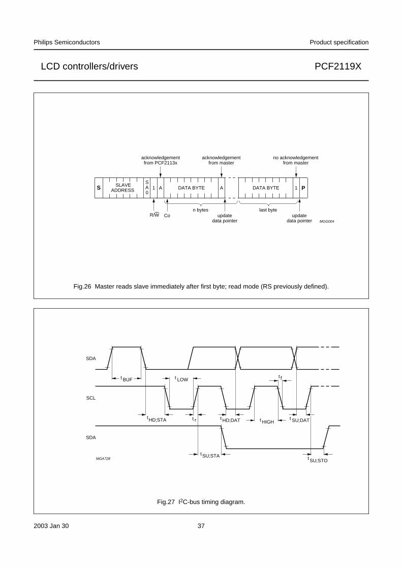
Fig.26 Master reads slave immediately after first byte; read mode (RS previously defined).
handbook, full pagewidth
MGG004
Co updatedata pointer
updatedata pointer
n bytes last byte
SA0
S 1 A DATA BYTE A 1 P SLAVEADDRESS DATA BYTE
acknowledgementfrom PCF2113x
acknowledgementfrom master
no acknowledgementfrom master
R/W
Fig.27 I2C-bus timing diagram.
handbook, full pagewidth
SDA
MGA728
SDA
SCL
tSU;STA t SU;STO
tHD;STA
t BUF t LOW
t HD;DAT t HIGHt r
t f
t SU;DAT
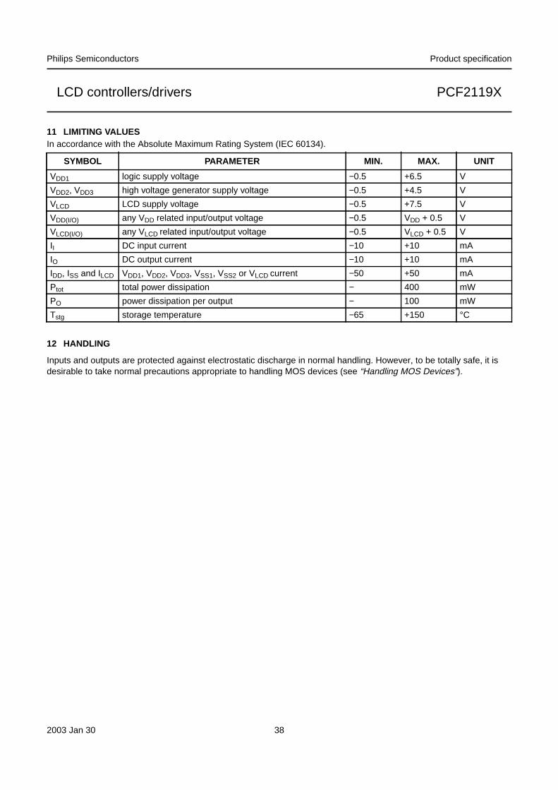
2003 Jan 30 38
Philips Semiconductors Product specification
LCD controllers/drivers PCF2119X
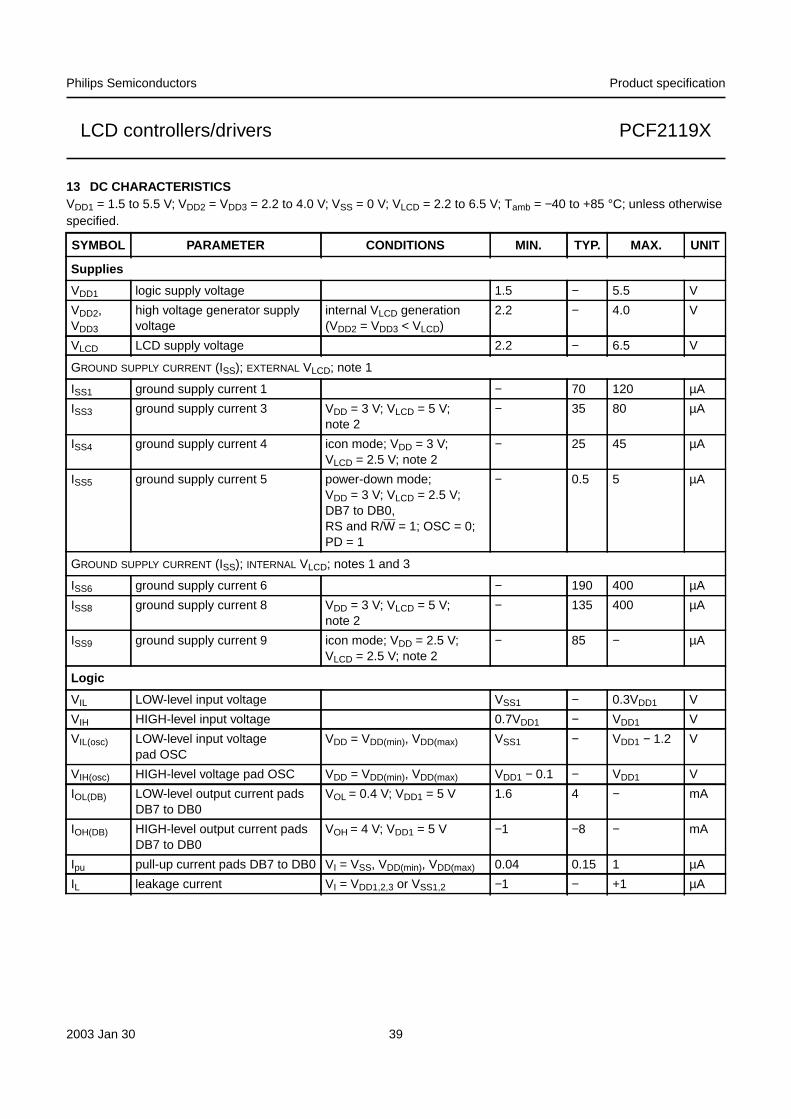
11 LIMITING VALUESIn accordance with the Absolute Maximum Rating System (IEC 60134).
12 HANDLING
Inputs and outputs are protected against electrostatic discharge in normal handling. However, to be totally safe, it isdesirable to take normal precautions appropriate to handling MOS devices (see “Handling MOS Devices”).
SYMBOL PARAMETER MIN. MAX. UNIT
VDD1 logic supply voltage −0.5 +6.5 V
VDD2, VDD3 high voltage generator supply voltage −0.5 +4.5 V
VLCD LCD supply voltage −0.5 +7.5 V
VDD(I/O) any VDD related input/output voltage −0.5 VDD + 0.5 V
VLCD(I/O) any VLCD related input/output voltage −0.5 VLCD + 0.5 V
II DC input current −10 +10 mA
IO DC output current −10 +10 mA
IDD, ISS and ILCD VDD1, VDD2, VDD3, VSS1, VSS2 or VLCD current −50 +50 mA
Ptot total power dissipation − 400 mW
PO power dissipation per output − 100 mW
Tstg storage temperature −65 +150 °C
2003 Jan 30 39
Philips Semiconductors Product specification
LCD controllers/drivers PCF2119X
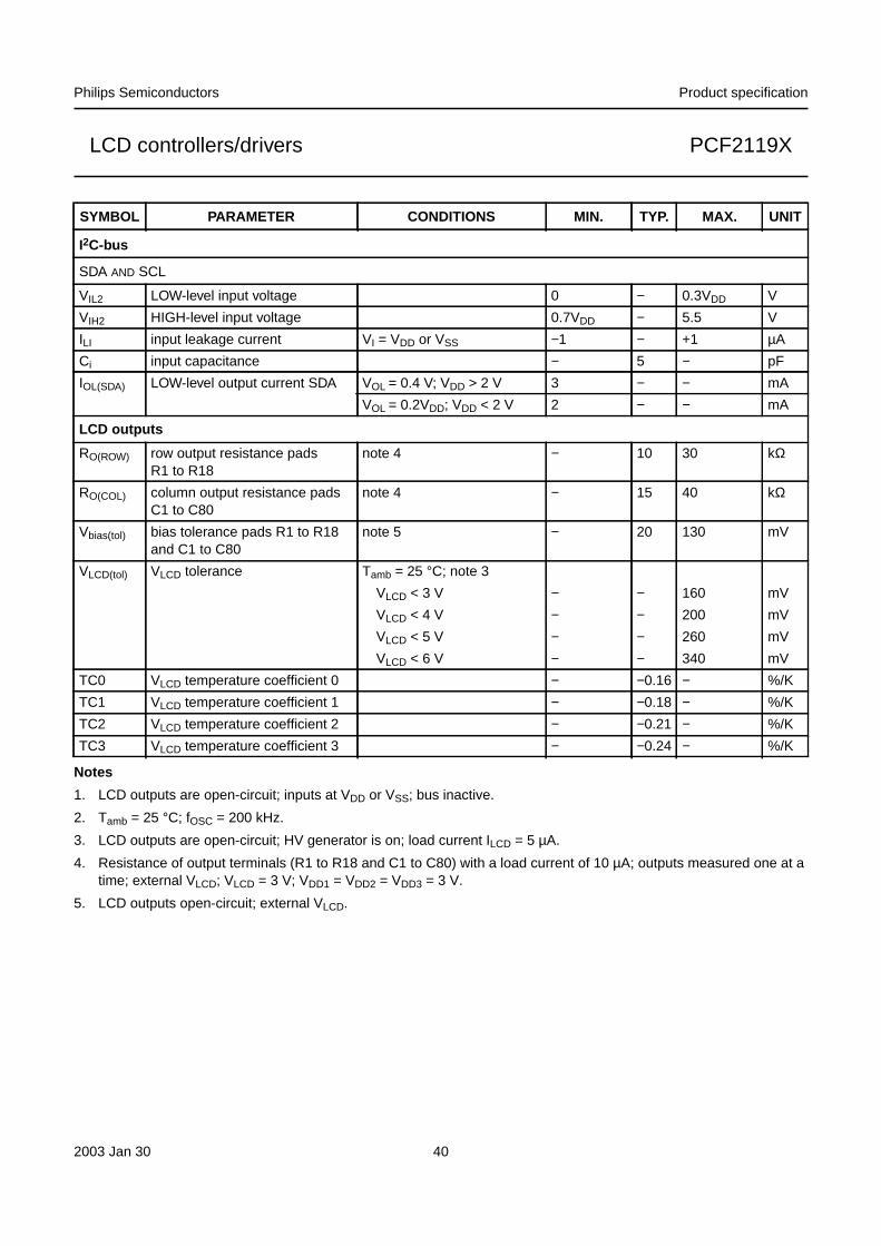
13 DC CHARACTERISTICSVDD1 = 1.5 to 5.5 V; VDD2 = VDD3 = 2.2 to 4.0 V; VSS = 0 V; VLCD = 2.2 to 6.5 V; Tamb = −40 to +85 °C; unless otherwisespecified.
SYMBOL PARAMETER CONDITIONS MIN. TYP. MAX. UNIT
Supplies
VDD1 logic supply voltage 1.5 − 5.5 V
VDD2,VDD3
high voltage generator supplyvoltage
internal VLCD generation(VDD2 = VDD3 < VLCD)
2.2 − 4.0 V
VLCD LCD supply voltage 2.2 − 6.5 V
GROUND SUPPLY CURRENT (ISS); EXTERNAL VLCD; note 1
ISS1 ground supply current 1 − 70 120 µA
ISS3 ground supply current 3 VDD = 3 V; VLCD = 5 V;note 2
− 35 80 µA
ISS4 ground supply current 4 icon mode; VDD = 3 V;VLCD = 2.5 V; note 2
− 25 45 µA
ISS5 ground supply current 5 power-down mode;VDD = 3 V; VLCD = 2.5 V;DB7 to DB0,RS and R/W = 1; OSC = 0;PD = 1
− 0.5 5 µA
GROUND SUPPLY CURRENT (ISS); INTERNAL VLCD; notes 1 and 3
ISS6 ground supply current 6 − 190 400 µA
ISS8 ground supply current 8 VDD = 3 V; VLCD = 5 V;note 2
− 135 400 µA
ISS9 ground supply current 9 icon mode; VDD = 2.5 V;VLCD = 2.5 V; note 2
− 85 − µA
Logic
VIL LOW-level input voltage VSS1 − 0.3VDD1 V
VIH HIGH-level input voltage 0.7VDD1 − VDD1 V
VIL(osc) LOW-level input voltagepad OSC
VDD = VDD(min), VDD(max) VSS1 − VDD1 − 1.2 V
VIH(osc) HIGH-level voltage pad OSC VDD = VDD(min), VDD(max) VDD1 − 0.1 − VDD1 V
IOL(DB) LOW-level output current padsDB7 to DB0
VOL = 0.4 V; VDD1 = 5 V 1.6 4 − mA
IOH(DB) HIGH-level output current padsDB7 to DB0
VOH = 4 V; VDD1 = 5 V −1 −8 − mA
Ipu pull-up current pads DB7 to DB0 VI = VSS, VDD(min), VDD(max) 0.04 0.15 1 µA
IL leakage current VI = VDD1,2,3 or VSS1,2 −1 − +1 µA
2003 Jan 30 40
Philips Semiconductors Product specification
LCD controllers/drivers PCF2119X
Notes
1. LCD outputs are open-circuit; inputs at VDD or VSS; bus inactive.
2. Tamb = 25 °C; fOSC = 200 kHz.
3. LCD outputs are open-circuit; HV generator is on; load current ILCD = 5 µA.
4. Resistance of output terminals (R1 to R18 and C1 to C80) with a load current of 10 µA; outputs measured one at atime; external VLCD; VLCD = 3 V; VDD1 = VDD2 = VDD3 = 3 V.
5. LCD outputs open-circuit; external VLCD.
I2C-bus
SDA AND SCL
VIL2 LOW-level input voltage 0 − 0.3VDD V
VIH2 HIGH-level input voltage 0.7VDD − 5.5 V
ILI input leakage current VI = VDD or VSS −1 − +1 µA
Ci input capacitance − 5 − pF
IOL(SDA) LOW-level output current SDA VOL = 0.4 V; VDD > 2 V 3 − − mA
VOL = 0.2VDD; VDD < 2 V 2 − − mA
LCD outputs
RO(ROW) row output resistance padsR1 to R18
note 4 − 10 30 kΩ
RO(COL) column output resistance padsC1 to C80
note 4 − 15 40 kΩ
Vbias(tol) bias tolerance pads R1 to R18and C1 to C80
note 5 − 20 130 mV
VLCD(tol) VLCD tolerance Tamb = 25 °C; note 3
VLCD < 3 V − − 160 mV
VLCD < 4 V − − 200 mV
VLCD < 5 V − − 260 mV
VLCD < 6 V − − 340 mV
TC0 VLCD temperature coefficient 0 − −0.16 − %/K
TC1 VLCD temperature coefficient 1 − −0.18 − %/K
TC2 VLCD temperature coefficient 2 − −0.21 − %/K
TC3 VLCD temperature coefficient 3 − −0.24 − %/K
SYMBOL PARAMETER CONDITIONS MIN. TYP. MAX. UNIT
2003 Jan 30 41
Philips Semiconductors Product specification
LCD controllers/drivers PCF2119X
14 AC CHARACTERISTICSVDD1 = 1.5 to 5.5 V; VDD2 = VDD3 = 2.2 to 4.0 V; VSS = 0 V; VLCD = 2.2 to 6.5 V; Tamb = −40 to +85 °C; unless otherwisespecified.
SYMBOL PARAMETER CONDITIONS MIN. TYP. MAX. UNIT
fFR LCD frame frequency (internal clock) VDD = 5.0 V 45 95 147 Hz
fOSC oscillator frequency (not available at anypad)
140 250 450 kHz
fOSC(ext) external clock frequency 140 − 450 kHz
tOSCST oscillator start-up time after power-down note 1 − 200 300 µs
Bus timing characteristics: parallel interface; note 2
WRITE OPERATION (WRITING DATA FROM MPU TO PCF2119X)
Tcy(en) enable cycle time 500 − − ns
tW(en) enable pulse width 220 − − ns
tsu(A) address set-up time 50 − − ns
th(A) address hold time 25 − − ns
tsu(D) data set-up time 60 − − ns
th(D) data hold time 25 − − ns
READ OPERATION (READING DATA FROM PCF2119X TO MPU)
Tcy(en) enable cycle time 500 − − ns
tW(en) enable pulse width 220 − − ns
tsu(A) address set-up time 50 − − ns
th(A) address hold time 25 − − ns
td(D) data delay time VDD1 > 2.2 V − − 150 ns
VDD1 > 1.5 V − − 250 ns
th(D) data hold time 20 − 100 ns
Timing characteristics: I 2C-bus interface; note 2
fSCL SCL clock frequency − − 400 kHz
tLOW SCL clock low period 1.3 − − µs
tHIGH SCL clock high period 0.6 − − µs
tSU;DAT data set-up time 100 − − ns
tHD;DAT data hold time 0 − − ns
tr SCL, SDA rise time notes 1 and 3 15 + 0.1CB − 300 ns
tf SCL, SDA fall time notes 1 and 3 15 + 0.1CB − 300 ns
CB capacitive bus line load − − 400 pF
tSU;STA set-up time for a repeated STARTcondition
0.6 − − µs
tHD;STA START condition hold time 0.6 − − µs
tSU;STO set-up time for STOP condition 0.6 − − µs
tSW tolerable spike width on bus − − 50 ns
tBUF bus free time between STOP and STARTcondition
1.3 − − µs
2003 Jan 30 42
Philips Semiconductors Product specification
LCD controllers/drivers PCF2119X
Notes
1. Tested on a sample basis.
2. All timing values are valid within the operating supply voltage and ambient temperature range and are referenced toVIL and VIH with an input voltage swing of VSS to VDD.
3. CB = total capacitance of one bus line in pF.
15 TIMING CHARACTERISTICS
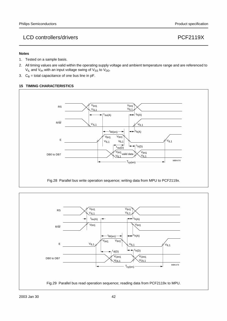
Fig.28 Parallel bus write operation sequence; writing data from MPU to PCF2119x.
handbook, full pagewidthRS
E
DB0 to DB7
V
V
V
VV
V
V
VV
V
V
V
V
T
IH1IL1
IH1IL1
IH1
IL1
IL1 IL1
IH1
IL1
IH1IL1VIL1
VIH1
IL1
cy(en)
t su(D) h(D)t
tW(en) th(A)
th(A)t su(A)
valid data
MBK474
R/W
handbook, full pagewidthRS
R/W
E
DB0 to DB7
V
V
VV
V
V
VV
VV
IH1
IL1
IH1IL1
IH1IL1
IH1IL1
VOL1
VOH1
IL1
Tcy(en)
h(D)t
tW(en) t h(A)
th(A)tsu(A)
IH1
VOL1
VOH1
td(D)
VIH1
MBK475
Fig.29 Parallel bus read operation sequence; reading data from PCF2119x to MPU.
2003 Jan 30 43
Philips Semiconductors Product specification
LCD controllers/drivers PCF2119X
16 APPLICATION INFORMATION
16.1 General information
The required minimum value for the external capacitors inan application with the PCF2119x are as follows: Cext forVLCD and VSS1,2 = 100 nF (min.), and for VDD1,2,3 andVSS1,2 = 470 nF. Higher capacitor values arerecommended for ripple rejection.
For COG applications the recommended ITO trackresistance is to be minimized for the I/O and supplyconnections. Optimized values for these are below 50 Ωfor the supply and below 100 Ω for the I/O connections.
Higher track resistance reduces performance andincreases current consumption.
To avoid accidental triggering of power-on reset(especially in COG applications), the supplies must beadequately decoupled. Depending on power supplyquality, VDD1 may have to be raised above the specifiedminimum value.
When external VLCD is supplied, VLCD2 should be leftopen-circuit to avoid any stray current, and VLCD1 must beconnected to VLCDSENSE.
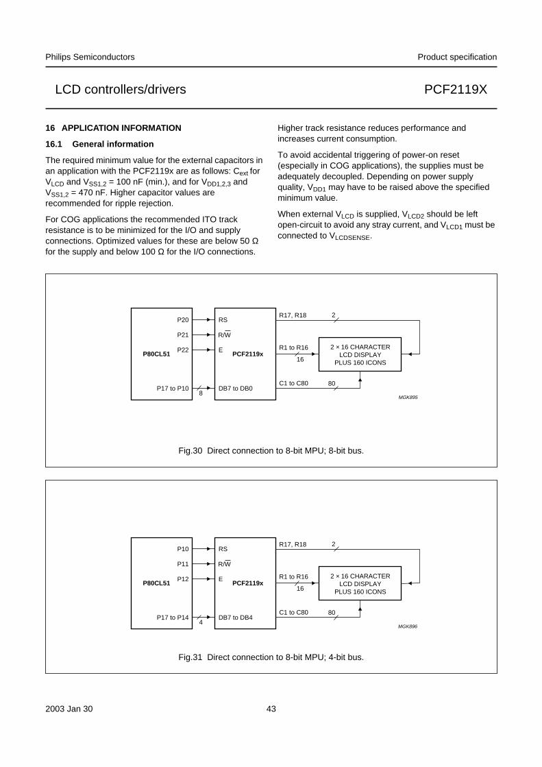
Fig.30 Direct connection to 8-bit MPU; 8-bit bus.
handbook, full pagewidth
PCF2119x
MGK895
P80CL512 × 16 CHARACTER
LCD DISPLAYPLUS 160 ICONS16
8
C1 to C80 80
2RSP20
P21
EP22
DB7 to DB0P17 to P10
R17, R18
R1 to R16
R/W
handbook, full pagewidth
PCF2119x
MGK896
P80CL512 × 16 CHARACTER
LCD DISPLAYPLUS 160 ICONS16
4
C1 to C80 80
2RSP10
P11
EP12
DB7 to DB4P17 to P14
R17, R18
R1 to R16
R/W
Fig.31 Direct connection to 8-bit MPU; 4-bit bus.
2003 Jan 30 44
Philips Semiconductors Product specification
LCD controllers/drivers PCF2119X
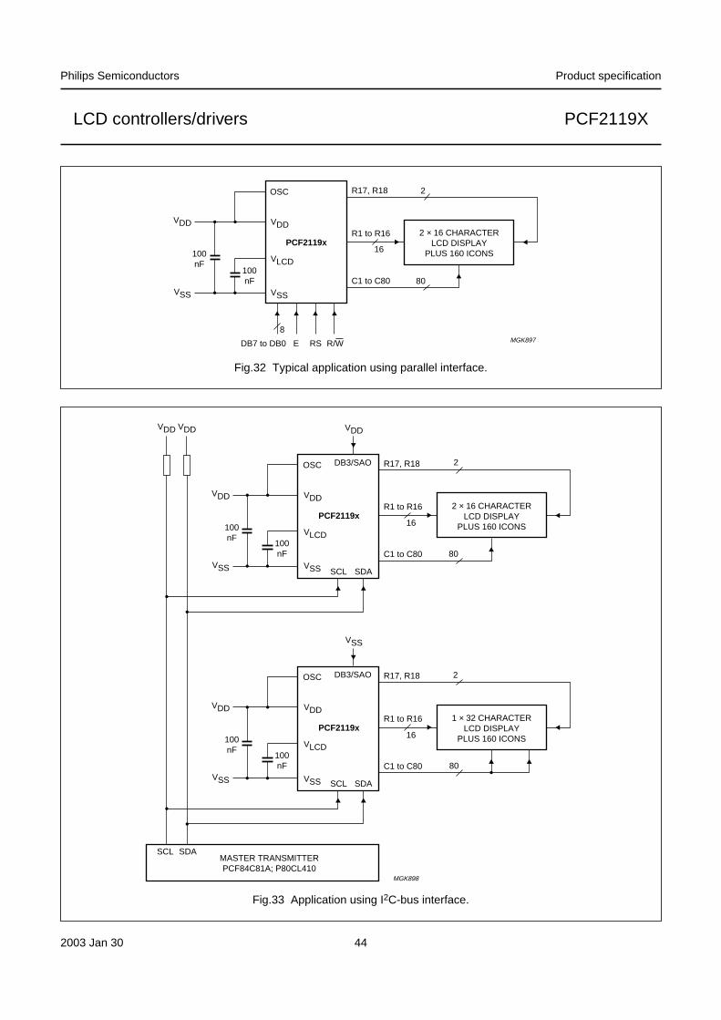
Fig.32 Typical application using parallel interface.
handbook, full pagewidth
MGK897
PCF2119x2 × 16 CHARACTER
LCD DISPLAYPLUS 160 ICONS16
8
C1 to C80 80
2OSC
RSDB7 to DB0 E
100nF
100nF
R17, R18
R1 to R16
VDD
VSS
VDD
VLCD
VSS
R/W
handbook, full pagewidth VDDVDD
SCL SDAMASTER TRANSMITTERPCF84C81A; P80CL410
PCF2119x2 × 16 CHARACTER
LCD DISPLAYPLUS 160 ICONS16
C1 to C80 80
2OSC
SCL SDA
DB3/SAO
100nF
100nF
R17, R18
R1 to R16
VDD
VDD
VSS
VDD
VLCD
VSS
PCF2119x1 × 32 CHARACTER
LCD DISPLAYPLUS 160 ICONS16
C1 to C80 80
2OSC
SCL SDA
DB3/SAO
100nF
100nF
R17, R18
R1 to R16
VSS
VDD
VSS
VDD
VLCD
VSS
MGK898
Fig.33 Application using I2C-bus interface.

2003 Jan 30 45
Philips Semiconductors Product specification
LCD controllers/drivers PCF2119X
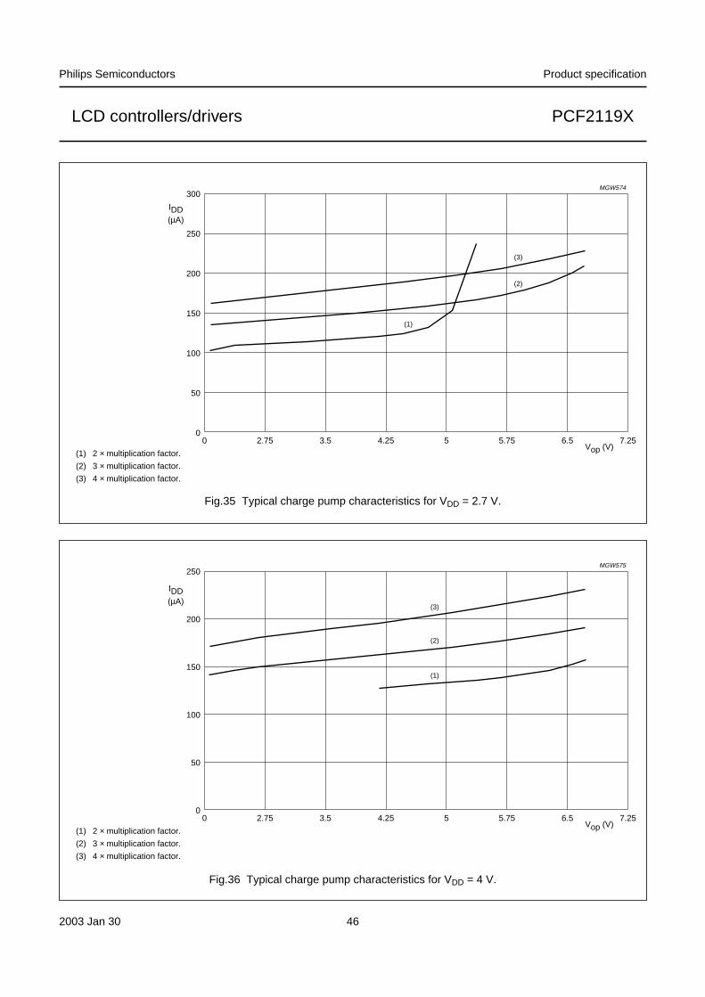
16.2 Charge pump characteristics
Typical graphs of the total power consumption of thePCF2119x using the internal charge pump are illustratedin Figs.34 to 36.
The graphs were obtained under the following conditions:
• Tamb = 25 °C• VDD1 = VDD2 = VDD3 = 2.2 V (min.), 2.7 V (typ.) and 4 V
(max.)
• Normal mode
• fosc = internal oscillator
• Mux 1 : 18
• Typical current load for ILCD = 10 µA.
For each multiplication factor there is a separate line. Theline ends where it is not possible to get a higher voltageunder its conditions (a higher multiplication factor isneeded to get higher voltages).
Connecting different displays may result in differentcurrent consumption. This affects the efficiency and theoptimum multiplication factor to be used to generate acertain output voltage.
handbook, full pagewidth
00
50
100
150
200
250
300
350
400
2.75 3.5 4.25 5 5.75 6.5 7.25Vop (V)
IDD(µA)
(1)
(2)
(3)
MGW573
Fig.34 Typical charge pump characteristics for VDD = 2.2 V.
(1) 2 × multiplication factor.
(2) 3 × multiplication factor.
(3) 4 × multiplication factor.
2003 Jan 30 46
Philips Semiconductors Product specification
LCD controllers/drivers PCF2119X
handbook, full pagewidth
00
50
100
150
200
250
300
2.75 3.5 4.25 5 5.75 6.5 7.25Vop (V)
IDD(µA)
(1)
(2)
(3)
MGW574
Fig.35 Typical charge pump characteristics for VDD = 2.7 V.
(1) 2 × multiplication factor.
(2) 3 × multiplication factor.
(3) 4 × multiplication factor.
handbook, full pagewidth
0
(1)
(2)
(3)
0
50
100
150
200
250
2.75 3.5 4.25 5 5.75 6.5 7.25Vop (V)
IDD(µA)
MGW575
Fig.36 Typical charge pump characteristics for VDD = 4 V.
(1) 2 × multiplication factor.
(2) 3 × multiplication factor.
(3) 4 × multiplication factor.
2003 Jan 30 47
Philips Semiconductors Product specification
LCD controllers/drivers PCF2119X
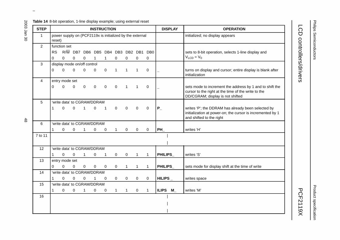
16.3 8-bit operation, 1-line display using externalreset
Table 14 shows an example of a 1-line display in 8-bitoperation. The PCF2119x functions must be set by the‘function set’ instruction prior to display. Since the DDRAMcan store data for 80 characters, the RAM can be used foradvertising displays when combined with display shiftoperation. Since the display shift operation changesdisplay position only and the DDRAM contents remainunchanged, display data entered first can be displayedwhen the ‘return home’ operation is performed.
16.4 4-bit operation, 1-line display using externalreset
The program must set functions prior to a 4-bit operation,see Table 13. When power is turned on, 8-bit operation isautomatically selected and the PCF2119x attempts toperform the first write as an 8-bit operation. Since nothingis connected to DB0 to DB3, a rewrite is then required.However, since one operation is completed in twoaccesses of 4-bit operation, a rewrite is required to set thefunctions (see Table 13 step 3). Thus, DB4 to DB7 of the‘function set’ are written twice.
16.5 8-bit operation, 2-line display
For a 2-line display, the cursor automatically moves fromthe first to the second line after the 40th digit of the first linehas been written. Thus, if there are only 8 characters in thefirst line, the DDRAM address must be set after the 8thcharacter is completed (see Table 6). It should be notedthat both lines of the display are always shifted together;data does not shift from one line to the other.
16.6 I2C-bus operation, 1-line display
A control byte is required with most commands(see Table 17).
Table 13 4-bit operation, 1-line display example; using external reset
STEP INSTRUCTION DISPLAY OPERATION
1 power supply on (PCF2119x is initialized bythe external reset)
initialized; no display appears
2 function set
RS R/W DB7 DB6 DB5 DB4 sets to 4-bit operation; in this instance operationis handled as 8-bits by initialization and only thisinstruction completes with one write
0 0 0 0 1 0
3 function set
0 0 0 0 1 0 sets to 4-bit operation, selects 1-line display andVLCD = V0; 4-bit operation starts from this pointand resetting is needed
0 0 0 0 0 0
4 display on/off control
0 0 0 0 0 0 _ turns on display and cursor; entire display isblank after initialization0 0 1 1 1 0
5 entry mode set
0 0 0 0 0 0 _ sets mode to increment the address by 1 and toshift the cursor to the right at the time of write tothe DD/CGRAM; display is not shifted
0 0 0 1 1 0
6 ‘write data’ to CGRAM/DDRAM
1 0 0 1 0 1 P_ writes ‘P’; the DDRAM has already been selectedby initialization at power-on; the cursor isincremented by 1 and shifted to the right
1 0 0 0 0 0
2003Jan
3048
Philips S
emiconductors
Product specification
LCD
controllers/driversP
CF
2119X
This text is here in white to force landscape pages to be rotated correctly when browsing through the pdf in the Acrobat reader.This text is here in_white to force landscape pages to be rotated correctly when browsing through the pdf in the Acrobat reader.This text is here inThis text is here inwhite to force landscape pages to be rotated correctly when browsing through the pdf in the Acrobat reader. white to force landscape pages to be ...
Table 14 8-bit operation, 1-line display example; using external reset
STEP INSTRUCTION DISPLAY OPERATION
1 power supply on (PCF2119x is initialized by the externalreset)
initialized; no display appears
2 function set
RS R/W DB7 DB6 DB5 DB4 DB3 DB2 DB1 DB0 sets to 8-bit operation, selects 1-line display andVLCD = V00 0 0 0 1 1 0 0 0 0
3 display mode on/off control
0 0 0 0 0 0 1 1 1 0 _ turns on display and cursor; entire display is blank afterinitialization
4 entry mode set
0 0 0 0 0 0 0 1 1 0 _ sets mode to increment the address by 1 and to shift thecursor to the right at the time of the write to theDD/CGRAM; display is not shifted
5 ‘write data’ to CGRAM/DDRAM
1 0 0 1 0 1 0 0 0 0 P_ writes ‘P’; the DDRAM has already been selected byinitialization at power-on; the cursor is incremented by 1and shifted to the right
6 ‘write data’ to CGRAM/DDRAM
1 0 0 1 0 0 1 0 0 0 PH_ writes ‘H’
7 to 11 |
|
12 ‘write data’ to CGRAM/DDRAM
1 0 0 1 0 1 0 0 1 1 PHILIPS_ writes ‘S’
13 entry mode set
0 0 0 0 0 0 0 1 1 1 PHILIPS_ sets mode for display shift at the time of write
14 ‘write data’ to CGRAM/DDRAM
1 0 0 0 1 0 0 0 0 0 HILIPS _ writes space
15 ‘write data’ to CGRAM/DDRAM
1 0 0 1 0 0 1 1 0 1 ILIPS M_ writes ‘M’
16 |
|
|
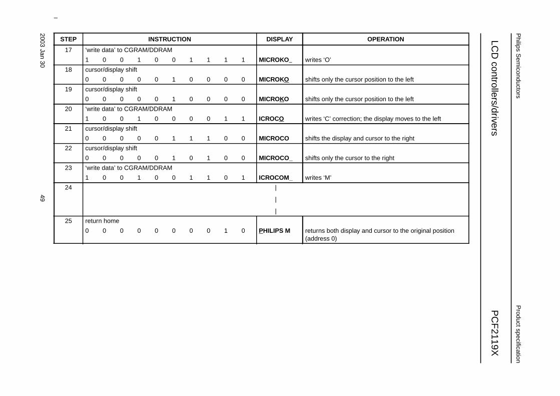
2003Jan
3049
Philips S
emiconductors
Product specification
LCD
controllers/driversP
CF
2119X
This text is here in white to force landscape pages to be rotated correctly when browsing through the pdf in the Acrobat reader.This text is here in_white to force landscape pages to be rotated correctly when browsing through the pdf in the Acrobat reader.This text is here inThis text is here inwhite to force landscape pages to be rotated correctly when browsing through the pdf in the Acrobat reader. white to force landscape pages to be ...
17 ‘write data’ to CGRAM/DDRAM
1 0 0 1 0 0 1 1 1 1 MICROKO writes ‘O’
18 cursor/display shift
0 0 0 0 0 1 0 0 0 0 MICROKO shifts only the cursor position to the left
19 cursor/display shift
0 0 0 0 0 1 0 0 0 0 MICROKO shifts only the cursor position to the left
20 ‘write data’ to CGRAM/DDRAM
1 0 0 1 0 0 0 0 1 1 ICROCO writes ‘C’ correction; the display moves to the left
21 cursor/display shift
0 0 0 0 0 1 1 1 0 0 MICROCO shifts the display and cursor to the right
22 cursor/display shift
0 0 0 0 0 1 0 1 0 0 MICROCO_ shifts only the cursor to the right
23 ‘write data’ to CGRAM/DDRAM
1 0 0 1 0 0 1 1 0 1 ICROCOM_ writes ‘M’
24 |
|
|
25 return home
0 0 0 0 0 0 0 0 1 0 PHILIPS M returns both display and cursor to the original position(address 0)
STEP INSTRUCTION DISPLAY OPERATION
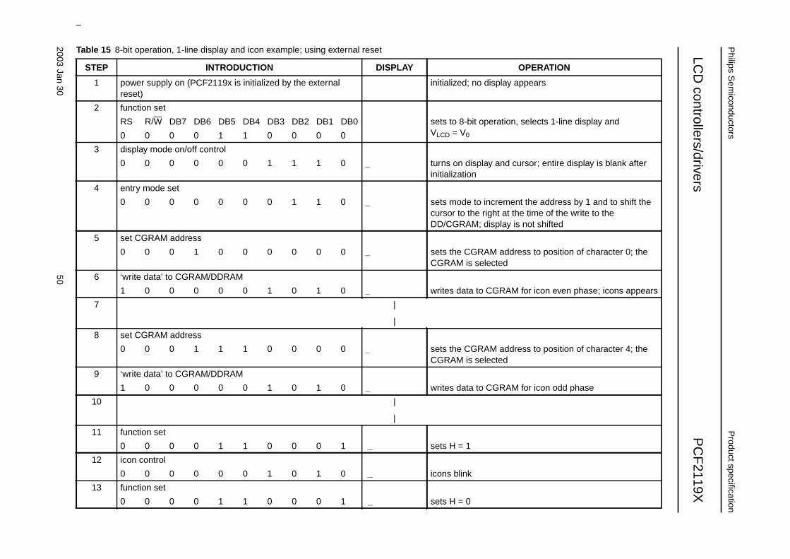
2003Jan
3050
Philips S
emiconductors
Product specification
LCD
controllers/driversP
CF
2119X
This text is here in white to force landscape pages to be rotated correctly when browsing through the pdf in the Acrobat reader.This text is here in_white to force landscape pages to be rotated correctly when browsing through the pdf in the Acrobat reader.This text is here inThis text is here inwhite to force landscape pages to be rotated correctly when browsing through the pdf in the Acrobat reader. white to force landscape pages to be ...
Table 15 8-bit operation, 1-line display and icon example; using external reset
STEP INTRODUCTION DISPLAY OPERATION
1 power supply on (PCF2119x is initialized by the externalreset)
initialized; no display appears
2 function set
RS R/W DB7 DB6 DB5 DB4 DB3 DB2 DB1 DB0 sets to 8-bit operation, selects 1-line display andVLCD = V00 0 0 0 1 1 0 0 0 0
3 display mode on/off control
0 0 0 0 0 0 1 1 1 0 _ turns on display and cursor; entire display is blank afterinitialization
4 entry mode set
0 0 0 0 0 0 0 1 1 0 _ sets mode to increment the address by 1 and to shift thecursor to the right at the time of the write to theDD/CGRAM; display is not shifted
5 set CGRAM address
0 0 0 1 0 0 0 0 0 0 _ sets the CGRAM address to position of character 0; theCGRAM is selected
6 ‘write data’ to CGRAM/DDRAM
1 0 0 0 0 0 1 0 1 0 _ writes data to CGRAM for icon even phase; icons appears
7 |
|
8 set CGRAM address
0 0 0 1 1 1 0 0 0 0 _ sets the CGRAM address to position of character 4; theCGRAM is selected
9 ‘write data’ to CGRAM/DDRAM
1 0 0 0 0 0 1 0 1 0 _ writes data to CGRAM for icon odd phase
10 |
|
11 function set
0 0 0 0 1 1 0 0 0 1 _ sets H = 1
12 icon control
0 0 0 0 0 0 1 0 1 0 _ icons blink
13 function set
0 0 0 0 1 1 0 0 0 1 _ sets H = 0
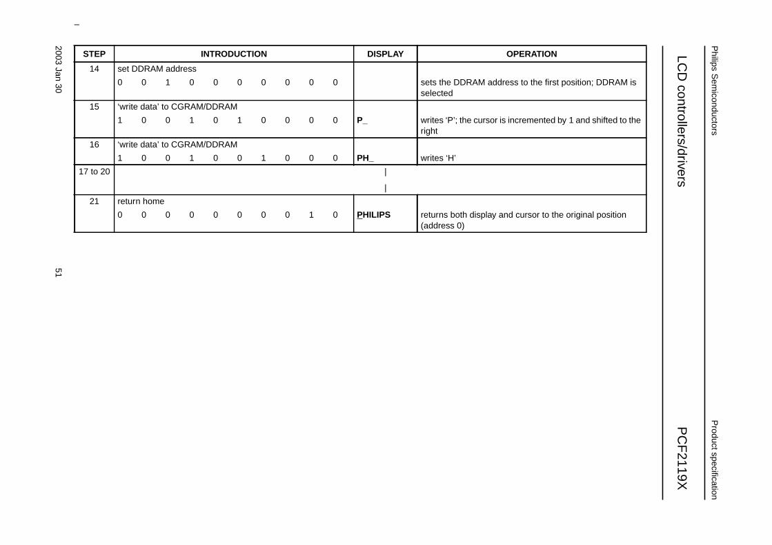
2003Jan
3051
Philips S
emiconductors
Product specification
LCD
controllers/driversP
CF
2119X
This text is here in white to force landscape pages to be rotated correctly when browsing through the pdf in the Acrobat reader.This text is here in_white to force landscape pages to be rotated correctly when browsing through the pdf in the Acrobat reader.This text is here inThis text is here inwhite to force landscape pages to be rotated correctly when browsing through the pdf in the Acrobat reader. white to force landscape pages to be ...
14 set DDRAM address
0 0 1 0 0 0 0 0 0 0 sets the DDRAM address to the first position; DDRAM isselected
15 ‘write data’ to CGRAM/DDRAM
1 0 0 1 0 1 0 0 0 0 P_ writes ‘P’; the cursor is incremented by 1 and shifted to theright
16 ‘write data’ to CGRAM/DDRAM
1 0 0 1 0 0 1 0 0 0 PH_ writes ‘H’
17 to 20 |
|
21 return home
0 0 0 0 0 0 0 0 1 0 PHILIPS returns both display and cursor to the original position(address 0)
STEP INTRODUCTION DISPLAY OPERATION
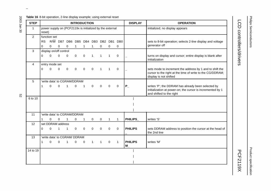
2003Jan
3052
Philips S
emiconductors
Product specification
LCD
controllers/driversP
CF
2119X
This text is here in white to force landscape pages to be rotated correctly when browsing through the pdf in the Acrobat reader.This text is here in_white to force landscape pages to be rotated correctly when browsing through the pdf in the Acrobat reader.This text is here inThis text is here inwhite to force landscape pages to be rotated correctly when browsing through the pdf in the Acrobat reader. white to force landscape pages to be ...
Table 16 8-bit operation, 2-line display example; using external reset
STEP INTRODUCTION DISPLAY OPERATION
1 power supply on (PCF2119x is initialized by the externalreset)
initialized; no display appears
2 function set
RS R/W DB7 DB6 DB5 DB4 DB3 DB2 DB1 DB0 sets to 8-bit operation; selects 2-line display and voltagegenerator off0 0 0 0 1 1 1 0 0 0
3 display on/off control
0 0 0 0 0 0 1 1 1 0 _ turns on display and cursor; entire display is blank afterinitialization
4 entry mode set
0 0 0 0 0 0 0 1 1 0 _ sets mode to increment the address by 1 and to shift thecursor to the right at the time of write to the CG/DDRAM;display is not shifted
5 ‘write data’ to CGRAM/DDRAM
1 0 0 1 0 1 0 0 0 0 P_ writes ‘P’; the DDRAM has already been selected byinitialization at power-on; the cursor is incremented by 1and shifted to the right
6 to 10 |
|
|
11 ‘write data’ to CGRAM/DDRAM
1 0 0 1 0 1 0 0 1 1 PHILIPS_ writes ‘S’
12 set DDRAM address
0 0 1 1 0 0 0 0 0 0 PHILIPS_
sets DDRAM address to position the cursor at the head ofthe 2nd line
13 ‘write data’ to CGRAM/ DDRAM
1 0 0 1 0 0 1 1 0 1 PHILIPSM_
writes ‘M’
14 to 19 |
|
|
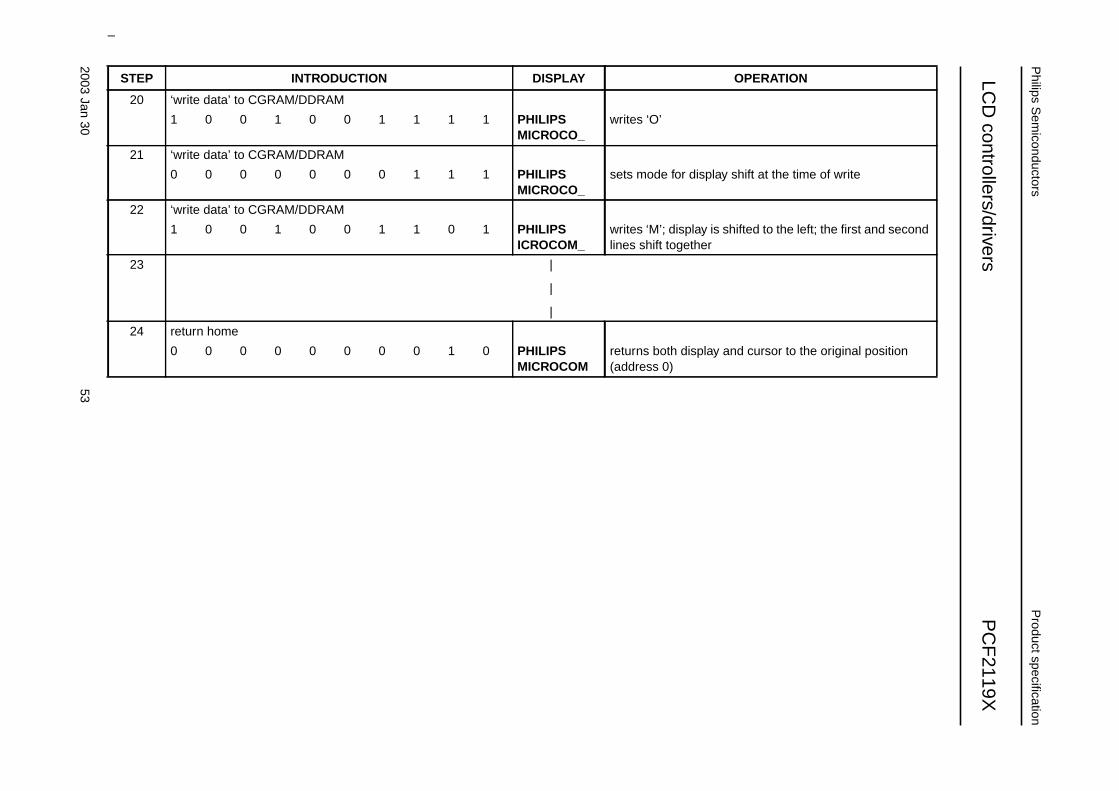
2003Jan
3053
Philips S
emiconductors
Product specification
LCD
controllers/driversP
CF
2119X
This text is here in white to force landscape pages to be rotated correctly when browsing through the pdf in the Acrobat reader.This text is here in_white to force landscape pages to be rotated correctly when browsing through the pdf in the Acrobat reader.This text is here inThis text is here inwhite to force landscape pages to be rotated correctly when browsing through the pdf in the Acrobat reader. white to force landscape pages to be ...
20 ‘write data’ to CGRAM/DDRAM
1 0 0 1 0 0 1 1 1 1 PHILIPSMICROCO_
writes ‘O’
21 ‘write data’ to CGRAM/DDRAM
0 0 0 0 0 0 0 1 1 1 PHILIPSMICROCO_
sets mode for display shift at the time of write
22 ‘write data’ to CGRAM/DDRAM
1 0 0 1 0 0 1 1 0 1 PHILIPSICROCOM_
writes ‘M’; display is shifted to the left; the first and secondlines shift together
23 |
|
|
24 return home
0 0 0 0 0 0 0 0 1 0 PHILIPSMICROCOM
returns both display and cursor to the original position(address 0)
STEP INTRODUCTION DISPLAY OPERATION
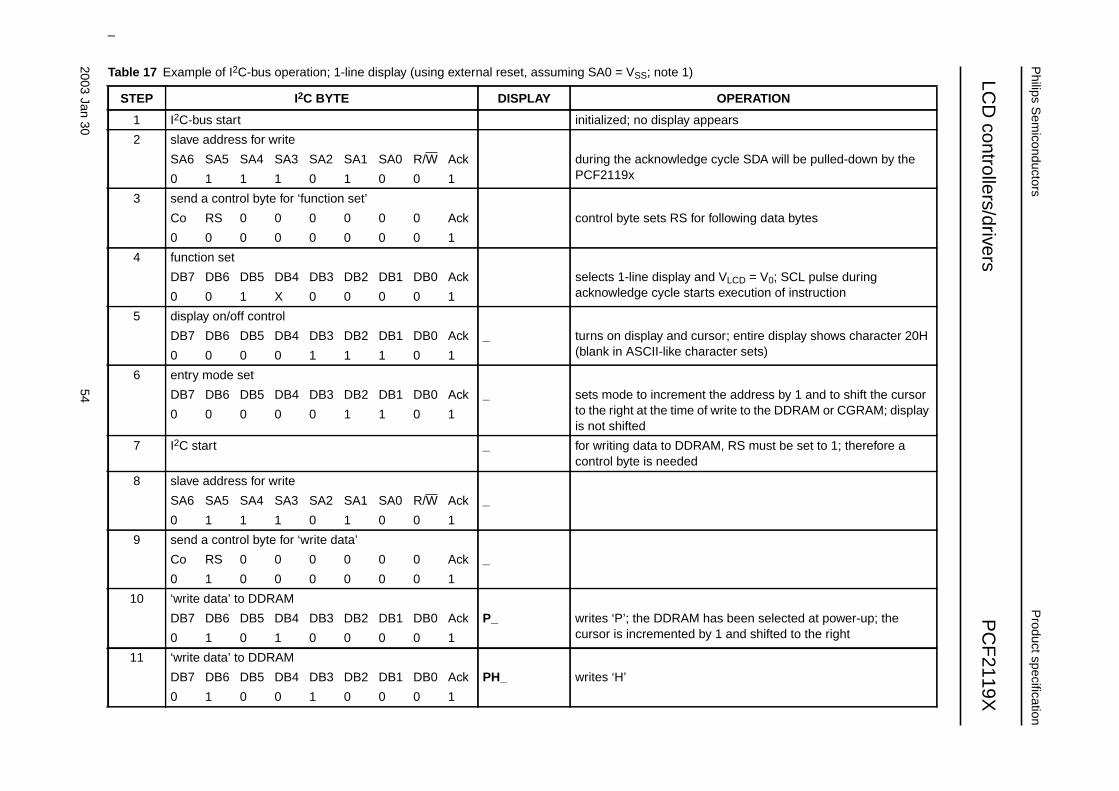
2003Jan
3054
Philips S
emiconductors
Product specification
LCD
controllers/driversP
CF
2119X
This text is here in white to force landscape pages to be rotated correctly when browsing through the pdf in the Acrobat reader.This text is here in_white to force landscape pages to be rotated correctly when browsing through the pdf in the Acrobat reader.This text is here inThis text is here inwhite to force landscape pages to be rotated correctly when browsing through the pdf in the Acrobat reader. white to force landscape pages to be ...
Table 17 Example of I2C-bus operation; 1-line display (using external reset, assuming SA0 = VSS; note 1)
STEP I2C BYTE DISPLAY OPERATION
1 I2C-bus start initialized; no display appears
2 slave address for write
SA6 SA5 SA4 SA3 SA2 SA1 SA0 R/W Ack during the acknowledge cycle SDA will be pulled-down by thePCF2119x0 1 1 1 0 1 0 0 1
3 send a control byte for ‘function set’
Co RS 0 0 0 0 0 0 Ack control byte sets RS for following data bytes
0 0 0 0 0 0 0 0 1
4 function set
DB7 DB6 DB5 DB4 DB3 DB2 DB1 DB0 Ack selects 1-line display and VLCD = V0; SCL pulse duringacknowledge cycle starts execution of instruction0 0 1 X 0 0 0 0 1
5 display on/off control
DB7 DB6 DB5 DB4 DB3 DB2 DB1 DB0 Ack _ turns on display and cursor; entire display shows character 20H(blank in ASCII-like character sets)0 0 0 0 1 1 1 0 1
6 entry mode set
DB7 DB6 DB5 DB4 DB3 DB2 DB1 DB0 Ack _ sets mode to increment the address by 1 and to shift the cursorto the right at the time of write to the DDRAM or CGRAM; displayis not shifted
0 0 0 0 0 1 1 0 1
7 I2C start _ for writing data to DDRAM, RS must be set to 1; therefore acontrol byte is needed
8 slave address for write
SA6 SA5 SA4 SA3 SA2 SA1 SA0 R/W Ack _
0 1 1 1 0 1 0 0 1
9 send a control byte for ‘write data’
Co RS 0 0 0 0 0 0 Ack _
0 1 0 0 0 0 0 0 1
10 ‘write data’ to DDRAM
DB7 DB6 DB5 DB4 DB3 DB2 DB1 DB0 Ack P_ writes ‘P’; the DDRAM has been selected at power-up; thecursor is incremented by 1 and shifted to the right0 1 0 1 0 0 0 0 1
11 ‘write data’ to DDRAM
DB7 DB6 DB5 DB4 DB3 DB2 DB1 DB0 Ack PH_ writes ‘H’
0 1 0 0 1 0 0 0 1
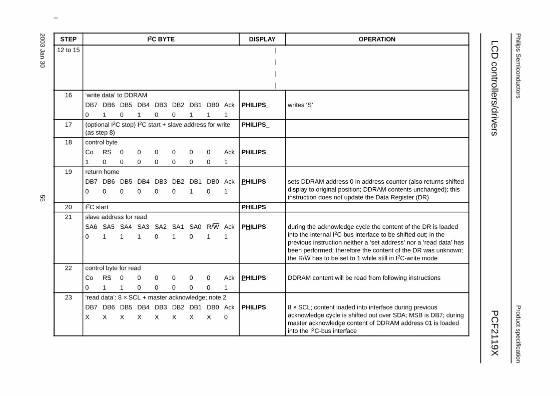
2003Jan
3055
Philips S
emiconductors
Product specification
LCD
controllers/driversP
CF
2119X
This text is here in white to force landscape pages to be rotated correctly when browsing through the pdf in the Acrobat reader.This text is here in_white to force landscape pages to be rotated correctly when browsing through the pdf in the Acrobat reader.This text is here inThis text is here inwhite to force landscape pages to be rotated correctly when browsing through the pdf in the Acrobat reader. white to force landscape pages to be ...
12 to 15 |
|
|
|
16 ‘write data’ to DDRAM
DB7 DB6 DB5 DB4 DB3 DB2 DB1 DB0 Ack PHILIPS_ writes ‘S’
0 1 0 1 0 0 1 1 1
17 (optional I2C stop) I2C start + slave address for write(as step 8)
PHILIPS_
18 control byte
Co RS 0 0 0 0 0 0 Ack PHILIPS_
1 0 0 0 0 0 0 0 1
19 return home
DB7 DB6 DB5 DB4 DB3 DB2 DB1 DB0 Ack PHILIPS sets DDRAM address 0 in address counter (also returns shifteddisplay to original position; DDRAM contents unchanged); thisinstruction does not update the Data Register (DR)
0 0 0 0 0 0 1 0 1
20 I2C start PHILIPS
21 slave address for read
SA6 SA5 SA4 SA3 SA2 SA1 SA0 R/W Ack PHILIPS during the acknowledge cycle the content of the DR is loadedinto the internal I2C-bus interface to be shifted out; in theprevious instruction neither a ‘set address’ nor a ‘read data’ hasbeen performed; therefore the content of the DR was unknown;the R/W has to be set to 1 while still in I2C-write mode
0 1 1 1 0 1 0 1 1
22 control byte for read
Co RS 0 0 0 0 0 0 Ack PHILIPS DDRAM content will be read from following instructions
0 1 1 0 0 0 0 0 1
23 ‘read data’: 8 × SCL + master acknowledge; note 2
DB7 DB6 DB5 DB4 DB3 DB2 DB1 DB0 Ack PHILIPS 8 × SCL; content loaded into interface during previousacknowledge cycle is shifted out over SDA; MSB is DB7; duringmaster acknowledge content of DDRAM address 01 is loadedinto the I2C-bus interface
X X X X X X X X 0
STEP I2C BYTE DISPLAY OPERATION
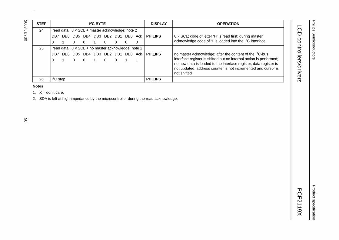
2003Jan
3056
Philips S
emiconductors
Product specification
LCD
controllers/driversP
CF
2119X
This text is here in white to force landscape pages to be rotated correctly when browsing through the pdf in the Acrobat reader.This text is here in_white to force landscape pages to be rotated correctly when browsing through the pdf in the Acrobat reader.This text is here inThis text is here inwhite to force landscape pages to be rotated correctly when browsing through the pdf in the Acrobat reader. white to force landscape pages to be ...
Notes
1. X = don’t care.
2. SDA is left at high-impedance by the microcontroller during the read acknowledge.
24 ‘read data’: 8 × SCL + master acknowledge; note 2
DB7 DB6 DB5 DB4 DB3 DB2 DB1 DB0 Ack PHILIPS 8 × SCL; code of letter ‘H’ is read first; during masteracknowledge code of ‘I’ is loaded into the I2C interface0 1 0 0 1 0 0 0 0
25 ‘read data’: 8 × SCL + no master acknowledge; note 2
DB7 DB6 DB5 DB4 DB3 DB2 DB1 DB0 Ack PHILIPS no master acknowledge; after the content of the I2C-businterface register is shifted out no internal action is performed;no new data is loaded to the interface register, data register isnot updated, address counter is not incremented and cursor isnot shifted
0 1 0 0 1 0 0 1 1
26 I2C stop PHILIPS
STEP I2C BYTE DISPLAY OPERATION
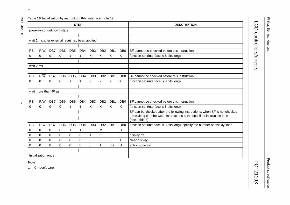
2003Jan
3057
Philips S
emiconductors
Product specification
LCD
controllers/driversP
CF
2119X
This text is here in white to force landscape pages to be rotated correctly when browsing through the pdf in the Acrobat reader.This text is here in_white to force landscape pages to be rotated correctly when browsing through the pdf in the Acrobat reader.This text is here inThis text is here inwhite to force landscape pages to be rotated correctly when browsing through the pdf in the Acrobat reader. white to force landscape pages to be ...
Table 18 Initialization by instruction, 8-bit interface (note 1)
Note
1. X = don’t care.
STEP DESCRIPTION
power-on or unknown state
|wait 2 ms after external reset has been applied
|RS R/W DB7 DB6 DB5 DB4 DB3 DB2 DB1 DB0 BF cannot be checked before this instruction
0 0 0 0 1 1 X X X X function set (interface is 8 bits long)
|wait 2 ms
|RS R/W DB7 DB6 DB5 DB4 DB3 DB2 DB1 DB0 BF cannot be checked before this instruction
0 0 0 0 1 1 X X X X function set (interface is 8 bits long)
|wait more than 40 µs
|RS R/W DB7 DB6 DB5 DB4 DB3 DB2 DB1 DB0 BF cannot be checked before this instruction
0 0 0 0 1 1 X X X X function set (interface is 8 bits long)
|
|
BF can be checked after the following instructions; when BF is not checked,the waiting time between instructions is the specified instruction time(see Table 3)
RS R/W DB7 DB6 DB5 DB4 DB3 DB2 DB1 DB0 function set (interface is 8 bits long); specify the number of display lines
0 0 0 0 1 1 0 M 0 H
0 0 0 0 0 0 1 0 0 0 display off
0 0 0 0 0 0 0 0 0 1 clear display
0 0 0 0 0 0 0 1 I/D S entry mode set
|Initialization ends
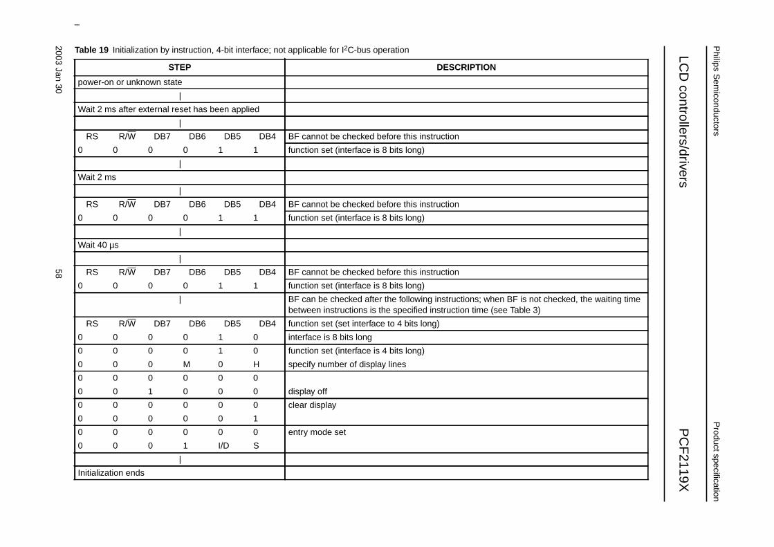
2003Jan
3058
Philips S
emiconductors
Product specification
LCD
controllers/driversP
CF
2119X
This text is here in white to force landscape pages to be rotated correctly when browsing through the pdf in the Acrobat reader.This text is here in_white to force landscape pages to be rotated correctly when browsing through the pdf in the Acrobat reader.This text is here inThis text is here inwhite to force landscape pages to be rotated correctly when browsing through the pdf in the Acrobat reader. white to force landscape pages to be ...
Table 19 Initialization by instruction, 4-bit interface; not applicable for I2C-bus operation
STEP DESCRIPTION
power-on or unknown state
|Wait 2 ms after external reset has been applied
|RS R/W DB7 DB6 DB5 DB4 BF cannot be checked before this instruction
0 0 0 0 1 1 function set (interface is 8 bits long)
|Wait 2 ms
|RS R/W DB7 DB6 DB5 DB4 BF cannot be checked before this instruction
0 0 0 0 1 1 function set (interface is 8 bits long)
|Wait 40 µs
|RS R/W DB7 DB6 DB5 DB4 BF cannot be checked before this instruction
0 0 0 0 1 1 function set (interface is 8 bits long)
| BF can be checked after the following instructions; when BF is not checked, the waiting timebetween instructions is the specified instruction time (see Table 3)
RS R/W DB7 DB6 DB5 DB4 function set (set interface to 4 bits long)
0 0 0 0 1 0 interface is 8 bits long
0 0 0 0 1 0 function set (interface is 4 bits long)
0 0 0 M 0 H specify number of display lines
0 0 0 0 0 0
0 0 1 0 0 0 display off
0 0 0 0 0 0 clear display
0 0 0 0 0 1
0 0 0 0 0 0 entry mode set
0 0 0 1 I/D S
|Initialization ends
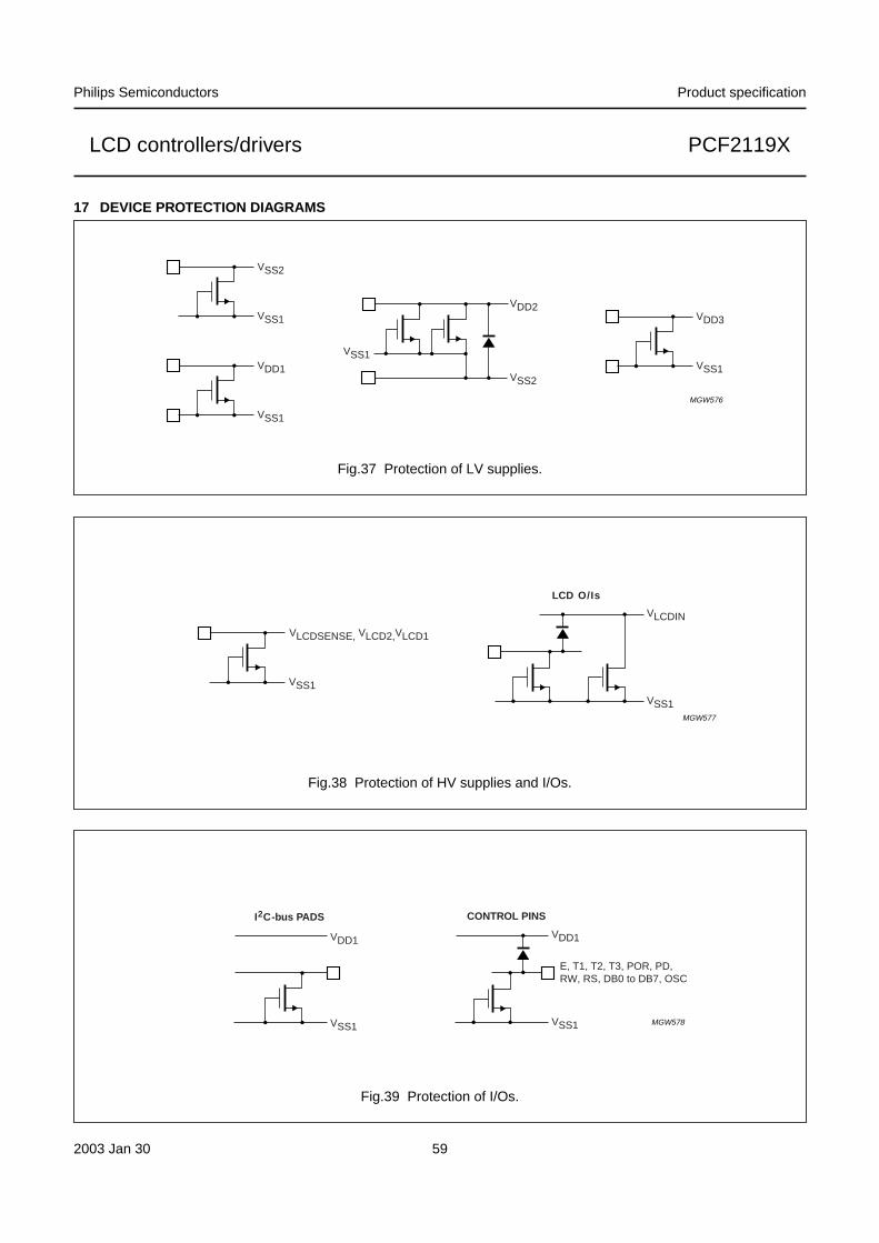
2003 Jan 30 59
Philips Semiconductors Product specification
LCD controllers/drivers PCF2119X
17 DEVICE PROTECTION DIAGRAMS
handbook, full pagewidth
MGW576
VSS2
VSS1
VDD1
VSS1
VDD3
VSS1
VDD2
VSS1
VSS2
Fig.37 Protection of LV supplies.
handbook, full pagewidth
MGW577
VSS1
VLCDIN
VSS1
VLCDSENSE, VLCD2,VLCD1
LCD O/Is
Fig.38 Protection of HV supplies and I/Os.
handbook, full pagewidth
MGW578
VDD1
VSS1
VDD1
E, T1, T2, T3, POR, PD,RW, RS, DB0 to DB7, OSC
VSS1
I2C-bus PADS CONTROL PINS
Fig.39 Protection of I/Os.
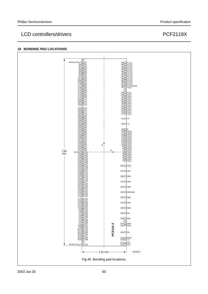
2003 Jan 30 60
Philips Semiconductors Product specification
LCD controllers/drivers PCF2119X
18 BONDING PAD LOCATIONS
handbook, full pagewidth
MGW572
10710610510410310210110099989796959493929190898887868584838281807978777675
74737271706968676665646362616059585756555453525150
108109110111112113114115116117118119120121122123124125
126127128129130131132133134135136137138139140141142143144145146147148149
150
C34C35C36C37C38C39C40
R17DUPC41C42C43C44C45C46C47C48C49C50C51C52C53C54C55C56C57C58C59C60C61C62C63C64C65
C66C67C68C69C70C71C72C73C74C75C76C77C78C79C80R17
R1R2R3R4R5R6R7R8
dummy (VSS1)
C33C32C31C30C29C28C27C26C25C24C23C22C21C20C19C18C17C16
C15C14C13C12C11C10
C9C8C7C6C5C4C3C2C1
R18R9
R10R11R12R13R14R15R16
dummy (VSS1)
PC
2119
-2
x
y
494847464544434241403938
1
151152
153154
155
156157
158
159
160
161
162
163
164
165
166
167
168
23456789
10111213141516171819
20
21
222324252627282930313233
3736
34
35
VLCD1VLCD1VLCD1VLCD1VLCD1VLCD1VLCD2VLCD2VLCD2VLCD2VLCD2VLCD2
VDD1
SCLSCL
T3POR
PD
SDASDA
RW
RS
DB0
DB1
DB2
DB3/SA0
DB4
DB5
DB6
DB7
OSC
VDD1VDD1VDD1VDD1VDD1VDD2VDD2VDD2VDD2VDD2VDD2VDD2VDD2VDD3VDD3VDD3VDD3E
T1
T2
VSS1VSS1VSS1VSS1VSS1VSS1VSS1VSS1VSS2VSS2VSS2VSS2
VLCD2VLCDSENSE
VSS2
VSS2
1.81 mm
7.64mm
Fig.40 Bonding pad locations.
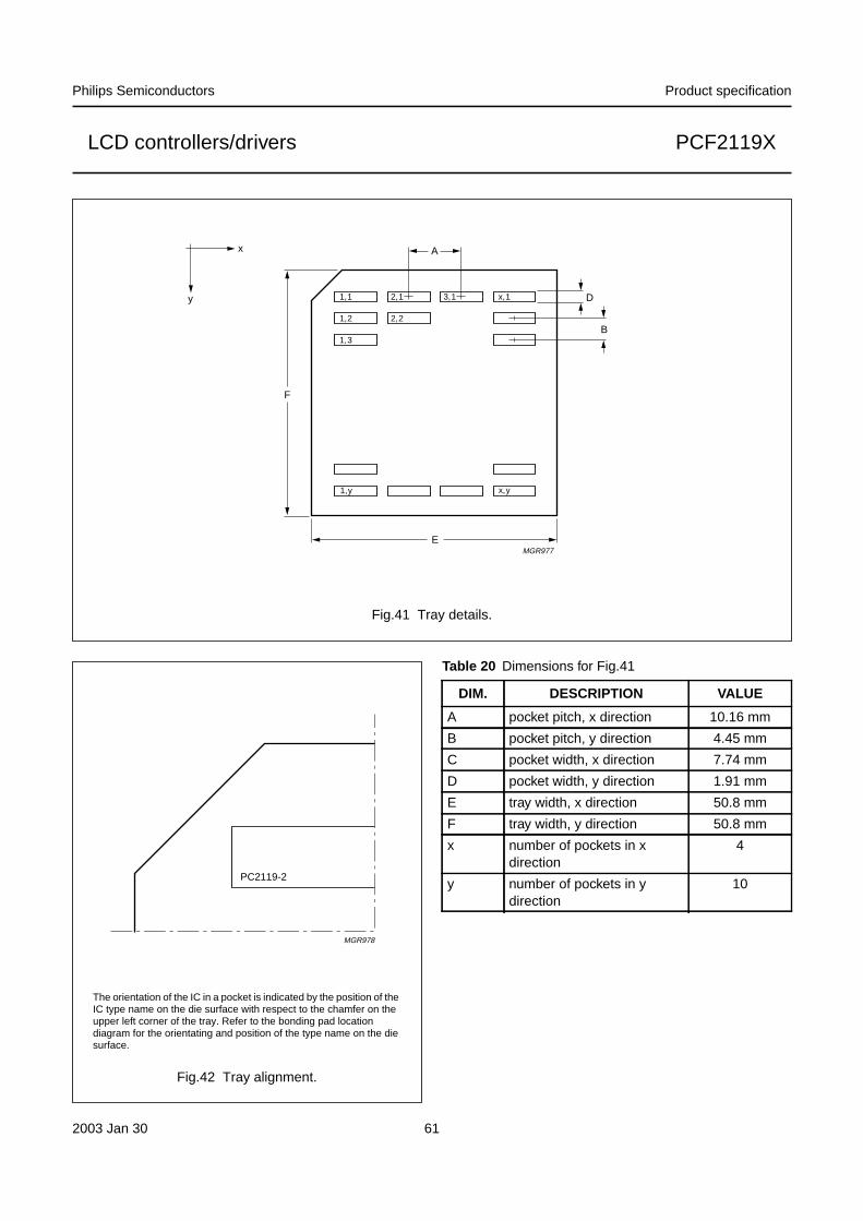
2003 Jan 30 61
Philips Semiconductors Product specification
LCD controllers/drivers PCF2119X
Fig.41 Tray details.
handbook, full pagewidth
MGR977
A
1,1
1,2
2,1 3,1 x,1
x,y1,y
2,2
1,3
E
x
y
F
D
B
Table 20 Dimensions for Fig.41
Fig.42 Tray alignment.
The orientation of the IC in a pocket is indicated by the position of theIC type name on the die surface with respect to the chamfer on theupper left corner of the tray. Refer to the bonding pad locationdiagram for the orientating and position of the type name on the diesurface.
MGR978
handbook, halfpage
PC2119-2
DIM. DESCRIPTION VALUE
A pocket pitch, x direction 10.16 mm
B pocket pitch, y direction 4.45 mm
C pocket width, x direction 7.74 mm
D pocket width, y direction 1.91 mm
E tray width, x direction 50.8 mm
F tray width, y direction 50.8 mm
x number of pockets in xdirection
4
y number of pockets in ydirection
10
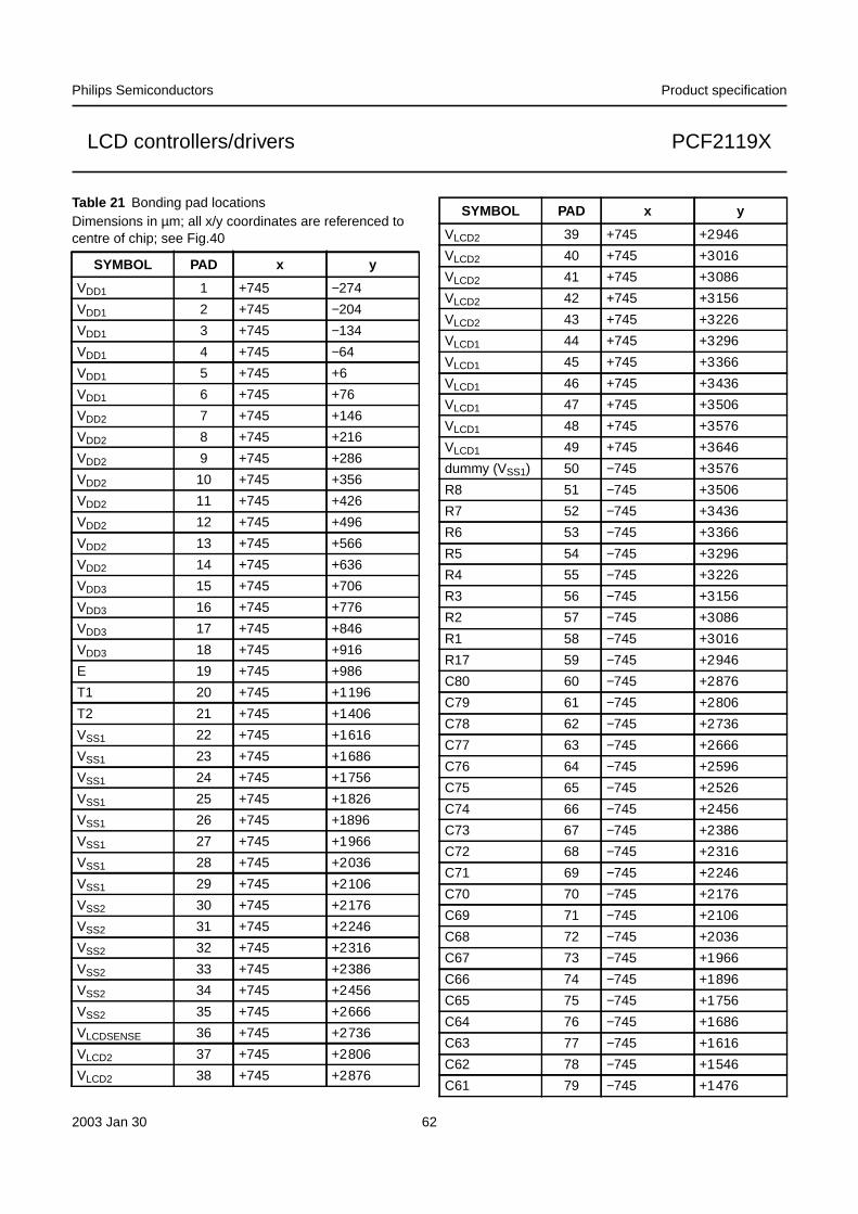
2003 Jan 30 62
Philips Semiconductors Product specification
LCD controllers/drivers PCF2119X
Table 21 Bonding pad locationsDimensions in µm; all x/y coordinates are referenced tocentre of chip; see Fig.40
SYMBOL PAD x y
VDD1 1 +745 −274
VDD1 2 +745 −204
VDD1 3 +745 −134
VDD1 4 +745 −64
VDD1 5 +745 +6
VDD1 6 +745 +76
VDD2 7 +745 +146
VDD2 8 +745 +216
VDD2 9 +745 +286
VDD2 10 +745 +356
VDD2 11 +745 +426
VDD2 12 +745 +496
VDD2 13 +745 +566
VDD2 14 +745 +636
VDD3 15 +745 +706
VDD3 16 +745 +776
VDD3 17 +745 +846
VDD3 18 +745 +916
E 19 +745 +986
T1 20 +745 +1196
T2 21 +745 +1406
VSS1 22 +745 +1616
VSS1 23 +745 +1686
VSS1 24 +745 +1756
VSS1 25 +745 +1826
VSS1 26 +745 +1896
VSS1 27 +745 +1966
VSS1 28 +745 +2036
VSS1 29 +745 +2106
VSS2 30 +745 +2176
VSS2 31 +745 +2246
VSS2 32 +745 +2316
VSS2 33 +745 +2386
VSS2 34 +745 +2456
VSS2 35 +745 +2666
VLCDSENSE 36 +745 +2736
VLCD2 37 +745 +2806
VLCD2 38 +745 +2876
VLCD2 39 +745 +2946
VLCD2 40 +745 +3016
VLCD2 41 +745 +3086
VLCD2 42 +745 +3156
VLCD2 43 +745 +3226
VLCD1 44 +745 +3296
VLCD1 45 +745 +3366
VLCD1 46 +745 +3436
VLCD1 47 +745 +3506
VLCD1 48 +745 +3576
VLCD1 49 +745 +3646
dummy (VSS1) 50 −745 +3576
R8 51 −745 +3506
R7 52 −745 +3436
R6 53 −745 +3366
R5 54 −745 +3296
R4 55 −745 +3226
R3 56 −745 +3156
R2 57 −745 +3086
R1 58 −745 +3016
R17 59 −745 +2946
C80 60 −745 +2876
C79 61 −745 +2806
C78 62 −745 +2736
C77 63 −745 +2666
C76 64 −745 +2596
C75 65 −745 +2526
C74 66 −745 +2456
C73 67 −745 +2386
C72 68 −745 +2316
C71 69 −745 +2246
C70 70 −745 +2176
C69 71 −745 +2106
C68 72 −745 +2036
C67 73 −745 +1966
C66 74 −745 +1896
C65 75 −745 +1756
C64 76 −745 +1686
C63 77 −745 +1616
C62 78 −745 +1546
C61 79 −745 +1476
SYMBOL PAD x y
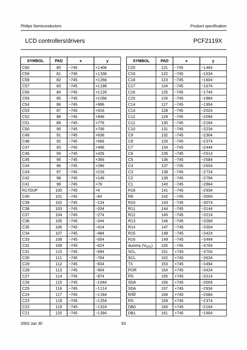
2003 Jan 30 63
Philips Semiconductors Product specification
LCD controllers/drivers PCF2119X
C60 80 −745 +1406
C59 81 −745 +1336
C58 82 −745 +1266
C57 83 −745 +1196
C56 84 −745 +1126
C55 85 −745 +1056
C54 86 −745 +986
C53 87 −745 +916
C52 88 −745 +846
C51 89 −745 +776
C50 90 −745 +706
C49 91 −745 +636
C48 92 −745 +566
C47 93 −745 +496
C46 94 −745 +426
C45 95 −745 +356
C44 96 −745 +286
C43 97 −745 +216
C42 98 −745 +146
C41 99 −745 +76
R17DUP 100 −745 +6
C40 101 −745 −64
C39 102 −745 −134
C38 103 −745 −204
C37 104 −745 −274
C36 105 −745 −344
C35 106 −745 −414
C34 107 −745 −484
C33 108 −745 −554
C32 109 −745 −624
C31 110 −745 −694
C30 111 −745 −764
C29 112 −745 −834
C28 113 −745 −904
C27 114 −745 −974
C26 115 −745 −1044
C25 116 −745 −1114
C24 117 −745 −1184
C23 118 −745 −1254
C22 119 −745 −1324
C21 120 −745 −1394
SYMBOL PAD x y
C20 121 −745 −1464
C19 122 −745 −1534
C18 123 −745 −1604
C17 124 −745 −1674
C16 125 −745 −1744
C15 126 −745 −1884
C14 127 −745 −1954
C13 128 −745 −2024
C12 129 −745 −2094
C11 130 −745 −2164
C10 131 −745 −2234
C9 132 −745 −2304
C8 133 −745 −2374
C7 134 −745 −2444
C6 135 −745 −2514
C5 136 −745 −2584
C4 137 −745 −2654
C3 138 −745 −2724
C2 139 −745 −2794
C1 140 −745 −2864
R18 141 −745 −2934
R9 142 −745 −3004
R10 143 −745 −3074
R11 144 −745 −3144
R12 145 −745 −3214
R13 146 −745 −3284
R14 147 −745 −3354
R15 148 −745 −3424
R16 149 −745 −3494
dummy (VSS1) 150 −745 −3704
SCL 151 +745 −3704
SCL 152 +745 −3634
T3 153 +745 −3494
POR 154 +745 −3424
PD 155 +745 −3214
SDA 156 +745 −3004
SDA 157 +745 −2934
R/W 158 +745 −2584
RS 159 +745 −2374
DB0 160 +745 −2164
DB1 161 +745 −1954
SYMBOL PAD x y
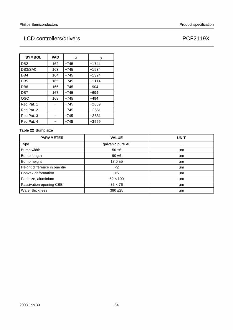
2003 Jan 30 64
Philips Semiconductors Product specification
LCD controllers/drivers PCF2119X
Table 22 Bump size
DB2 162 +745 −1744
DB3/SA0 163 +745 −1534
DB4 164 +745 −1324
DB5 165 +745 −1114
DB6 166 +745 −904
DB7 167 +745 −694
OSC 168 +745 −484
Rec.Pat. 1 − +745 −2689
Rec.Pat. 2 − +745 +2561
Rec.Pat. 3 − −745 +3681
Rec.Pat. 4 − −745 −3599
PARAMETER VALUE UNIT
Type galvanic pure Au −Bump width 50 ±6 µm
Bump length 90 ±6 µm
Bump height 17.5 ±5 µm
Height difference in one die <2 µm
Convex deformation <5 µm
Pad size, aluminium 62 × 100 µm
Passivation opening CBB 36 × 76 µm
Wafer thickness 380 ±25 µm
SYMBOL PAD x y
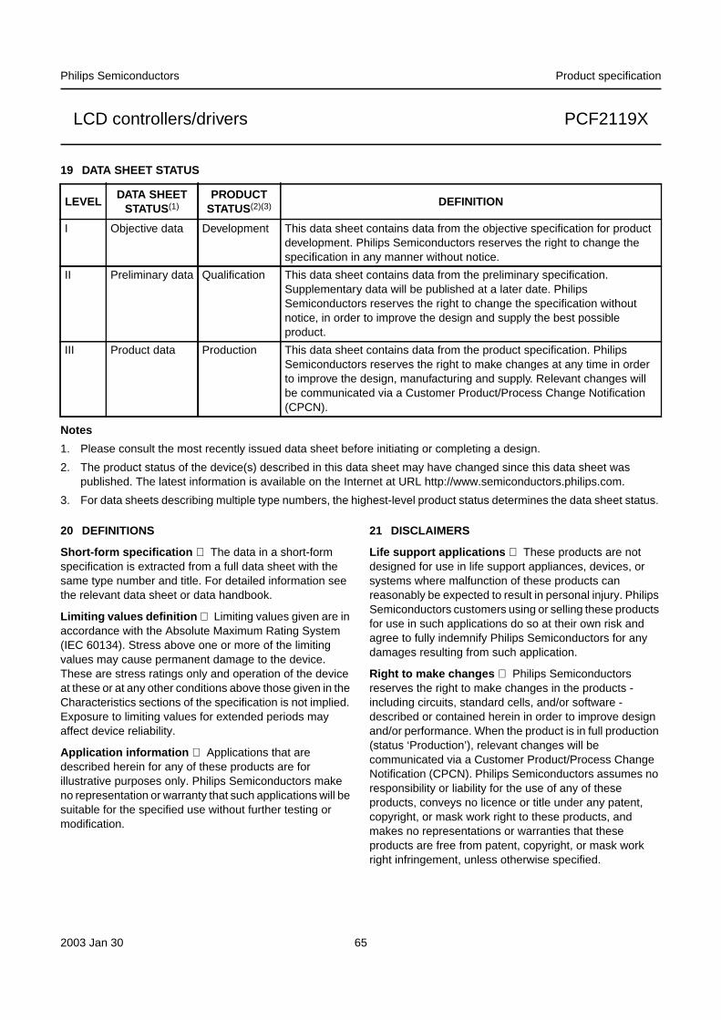
2003 Jan 30 65
Philips Semiconductors Product specification
LCD controllers/drivers PCF2119X
19 DATA SHEET STATUS
Notes
1. Please consult the most recently issued data sheet before initiating or completing a design.
2. The product status of the device(s) described in this data sheet may have changed since this data sheet waspublished. The latest information is available on the Internet at URL http://www.semiconductors.philips.com.
3. For data sheets describing multiple type numbers, the highest-level product status determines the data sheet status.
LEVELDATA SHEET
STATUS(1)PRODUCT
STATUS(2)(3) DEFINITION
I Objective data Development This data sheet contains data from the objective specification for productdevelopment. Philips Semiconductors reserves the right to change thespecification in any manner without notice.
II Preliminary data Qualification This data sheet contains data from the preliminary specification.Supplementary data will be published at a later date. PhilipsSemiconductors reserves the right to change the specification withoutnotice, in order to improve the design and supply the best possibleproduct.
III Product data Production This data sheet contains data from the product specification. PhilipsSemiconductors reserves the right to make changes at any time in orderto improve the design, manufacturing and supply. Relevant changes willbe communicated via a Customer Product/Process Change Notification(CPCN).
20 DEFINITIONS
Short-form specification The data in a short-formspecification is extracted from a full data sheet with thesame type number and title. For detailed information seethe relevant data sheet or data handbook.
Limiting values definition Limiting values given are inaccordance with the Absolute Maximum Rating System(IEC 60134). Stress above one or more of the limitingvalues may cause permanent damage to the device.These are stress ratings only and operation of the deviceat these or at any other conditions above those given in theCharacteristics sections of the specification is not implied.Exposure to limiting values for extended periods mayaffect device reliability.
Application information Applications that aredescribed herein for any of these products are forillustrative purposes only. Philips Semiconductors makeno representation or warranty that such applications will besuitable for the specified use without further testing ormodification.
21 DISCLAIMERS
Life support applications These products are notdesigned for use in life support appliances, devices, orsystems where malfunction of these products canreasonably be expected to result in personal injury. PhilipsSemiconductors customers using or selling these productsfor use in such applications do so at their own risk andagree to fully indemnify Philips Semiconductors for anydamages resulting from such application.
Right to make changes Philips Semiconductorsreserves the right to make changes in the products -including circuits, standard cells, and/or software -described or contained herein in order to improve designand/or performance. When the product is in full production(status ‘Production’), relevant changes will becommunicated via a Customer Product/Process ChangeNotification (CPCN). Philips Semiconductors assumes noresponsibility or liability for the use of any of theseproducts, conveys no licence or title under any patent,copyright, or mask work right to these products, andmakes no representations or warranties that theseproducts are free from patent, copyright, or mask workright infringement, unless otherwise specified.
2003 Jan 30 66
Philips Semiconductors Product specification
LCD controllers/drivers PCF2119X
22 PURCHASE OF PHILIPS I2C COMPONENTS
Purchase of Philips I2C components conveys a license under the Philips’ I2C patent to use thecomponents in the I2C system provided the system conforms to the I2C specification defined byPhilips. This specification can be ordered using the code 9398 393 40011.
2003 Jan 30 67
Philips Semiconductors Product specification
LCD controllers/drivers PCF2119X
NOTES

© Koninklijke Philips Electronics N.V. 2003 SCA75All rights are reserved. Reproduction in whole or in part is prohibited without the prior written consent of the copyright owner.
The information presented in this document does not form part of any quotation or contract, is believed to be accurate and reliable and may be changedwithout notice. No liability will be accepted by the publisher for any consequence of its use. Publication thereof does not convey nor imply any licenseunder patent- or other industrial or intellectual property rights.
Philips Semiconductors – a worldwide company
Contact information
For additional information please visit http://www.semiconductors.philips.com . Fax: +31 40 27 24825For sales offices addresses send e-mail to: [email protected] .
Printed in The Netherlands 403512/04/pp68 Date of release: 2003 Jan 30 Document order number: 9397 750 10483
Related Documents