1. General description The PCA9601 is designed to isolate I 2 C-bus capacitance, allowing long buses to be driven in point-to-point or multipoint applications of up to 4000 pF. The PCA9601 is a higher-speed version of the P82B96 and a higher drive version of the PCA9600 that allows many more Fast-mode Plus (Fm+) slaves on remote daughter cards in applications with temperature range of 0 C to 85 C. It creates a non-latching, bidirectional, logic interface between a normal I 2 C-bus and a range of other higher capacitance or different voltage bus configurations. It can operate at speeds up to at least 1 MHz, and the high drive side is compatible with the Fast-mode Plus specifications. The PCA9601 features temperature-stabilized logic voltage levels at its SX/SY interface making it suitable for interfacing with buses that have non I 2 C-bus-compliant logic levels such as SMBus, PMBus, or with microprocessors that use those same TTL logic levels. 15 mA drive capability over 0 C to 85 C at SX/SY allows driving a 5 V Fm+ bus with 470 pF loading. The separation of the bidirectional I 2 C-bus signals into unidirectional TX and RX signals enables the SDA and SCL signals to be transmitted via balanced transmission lines (twisted pairs), or with galvanic isolation using opto or magnetic coupling. The TX and RX signals may be connected together to provide a normal bidirectional signal. 2. Features and benefits Bidirectional data transfer of I 2 C-bus signals 15 mA SX/SY sink capability yields 5 V Fm+ bus rise time with 470 pF loads Isolates capacitance allowing > 400 pF on SX/SY side and 4000 pF on TX/TY side 1 MHz operation on up to 20 meters of wire (see AN10658) Supply voltage range of 2.5 V to 15 V with I 2 C-bus logic levels on SX/SY side independent of supply voltage Splits I 2 C-bus signal into pairs of forward/reverse TX/RX, TY/RY signals for interface with opto-electrical isolators and similar devices that need unidirectional input and output signal paths Low power supply current ESD protection exceeds 3500 V HBM per JESD22-A114, and 1400 V CDM per JESD22-C101 Latch-up testing is done to JEDEC Standard JESD78 which exceeds 100 mA Packages offered: SO8 and TSSOP8 (MSOP8) PCA9601 Dual bidirectional bus buffer Rev. 3 — 24 September 2015 Product data sheet

Welcome message from author
This document is posted to help you gain knowledge. Please leave a comment to let me know what you think about it! Share it to your friends and learn new things together.
Transcript
1. General description
The PCA9601 is designed to isolate I2C-bus capacitance, allowing long buses to be driven in point-to-point or multipoint applications of up to 4000 pF. The PCA9601 is a higher-speed version of the P82B96 and a higher drive version of the PCA9600 that allows many more Fast-mode Plus (Fm+) slaves on remote daughter cards in applications with temperature range of 0 C to 85 C.
It creates a non-latching, bidirectional, logic interface between a normal I2C-bus and a range of other higher capacitance or different voltage bus configurations. It can operate at speeds up to at least 1 MHz, and the high drive side is compatible with the Fast-mode Plus specifications.
The PCA9601 features temperature-stabilized logic voltage levels at its SX/SY interface making it suitable for interfacing with buses that have non I2C-bus-compliant logic levels such as SMBus, PMBus, or with microprocessors that use those same TTL logic levels.
15 mA drive capability over 0 C to 85 C at SX/SY allows driving a 5 V Fm+ bus with 470 pF loading.
The separation of the bidirectional I2C-bus signals into unidirectional TX and RX signals enables the SDA and SCL signals to be transmitted via balanced transmission lines (twisted pairs), or with galvanic isolation using opto or magnetic coupling. The TX and RX signals may be connected together to provide a normal bidirectional signal.
2. Features and benefits
Bidirectional data transfer of I2C-bus signals
15 mA SX/SY sink capability yields 5 V Fm+ bus rise time with 470 pF loads
Isolates capacitance allowing > 400 pF on SX/SY side and 4000 pF on TX/TY side
1 MHz operation on up to 20 meters of wire (see AN10658)
Supply voltage range of 2.5 V to 15 V with I2C-bus logic levels on SX/SY side independent of supply voltage
Splits I2C-bus signal into pairs of forward/reverse TX/RX, TY/RY signals for interface with opto-electrical isolators and similar devices that need unidirectional input and output signal paths
Low power supply current
ESD protection exceeds 3500 V HBM per JESD22-A114, and 1400 V CDM per JESD22-C101
Latch-up testing is done to JEDEC Standard JESD78 which exceeds 100 mA
Packages offered: SO8 and TSSOP8 (MSOP8)
PCA9601Dual bidirectional bus bufferRev. 3 — 24 September 2015 Product data sheet

NXP Semiconductors PCA9601Dual bidirectional bus buffer
3. Applications
Interface between I2C-buses operating at different logic levels (for example, 5 V and 3 V or 15 V)
Interface between I2C-bus and SMBus (350 A) standard or Fm+ standard
Simple conversion of I2C-bus SDA or SCL signals to multi-drop differential bus hardware, for example, via compatible PCA82C250
Interfaces with opto-couplers to provide opto-isolation between I2C-bus nodes up to 1 MHz
Long distance point-to-point or multipoint architectures
4. Ordering information
4.1 Ordering options
Table 1. Ordering information
Type number Topside marking
Package
Name Description Version
PCA9601D PCA9601 SO8 plastic small outline package; 8 leads; body width 3.9 mm SOT96-1
PCA9601DP 9601 TSSOP8 plastic thin shrink small outline package; 8 leads; body width 3 mm
SOT505-1
Table 2. Ordering options
Type number Orderable part number
Package Packing method Minimum order quantity
Temperature
PCA9601D PCA9601D,118 SO8 REEL 13" Q1/T1 *STANDARD MARK SMD
2500 Tamb = 40 C to +85 C
PCA9601DP PCA9601DP,118 TSSOP8 REEL 13" Q1/T1 *STANDARD MARK SMD
2500 Tamb = 40 C to +85 C
PCA9601 All information provided in this document is subject to legal disclaimers. © NXP Semiconductors N.V. 2015. All rights reserved.
Product data sheet Rev. 3 — 24 September 2015 2 of 32
NXP Semiconductors PCA9601Dual bidirectional bus buffer
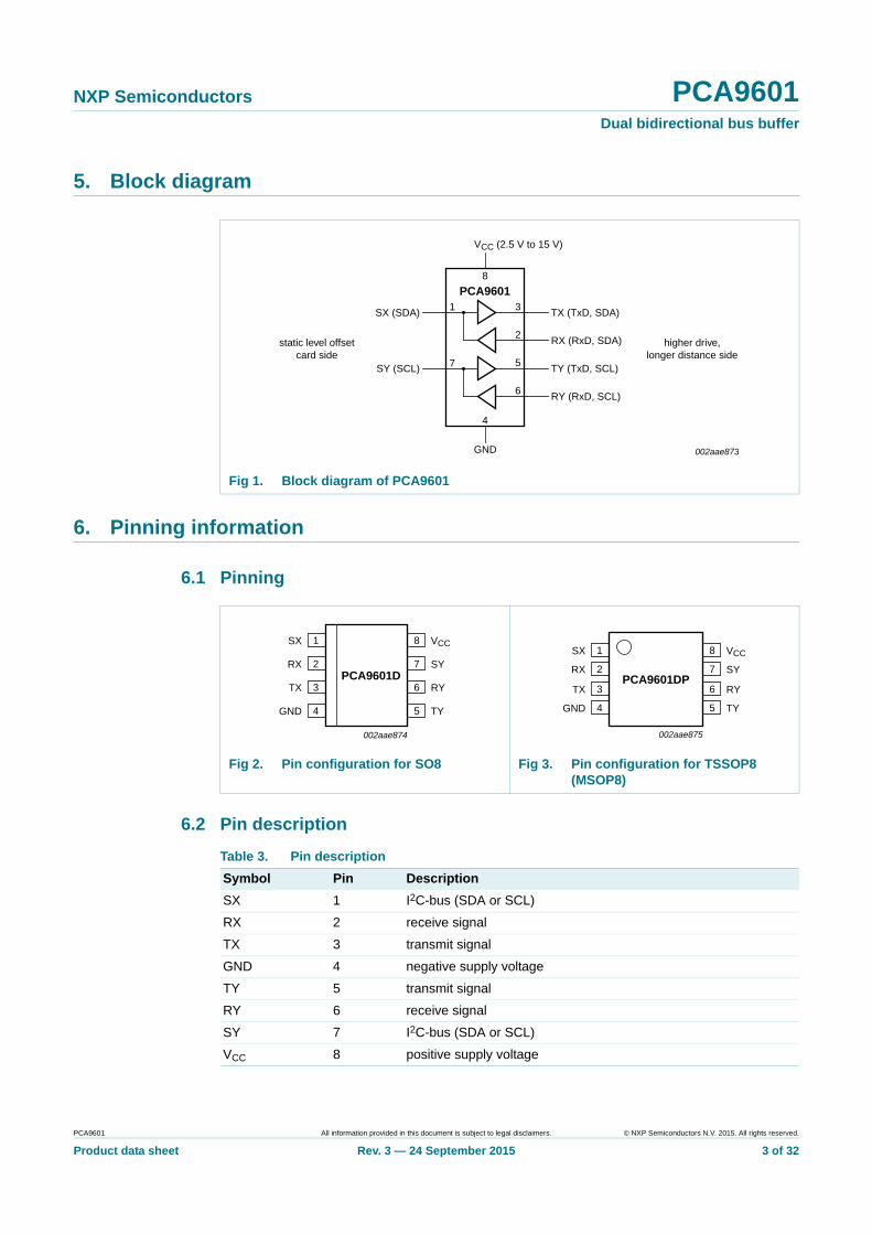
5. Block diagram
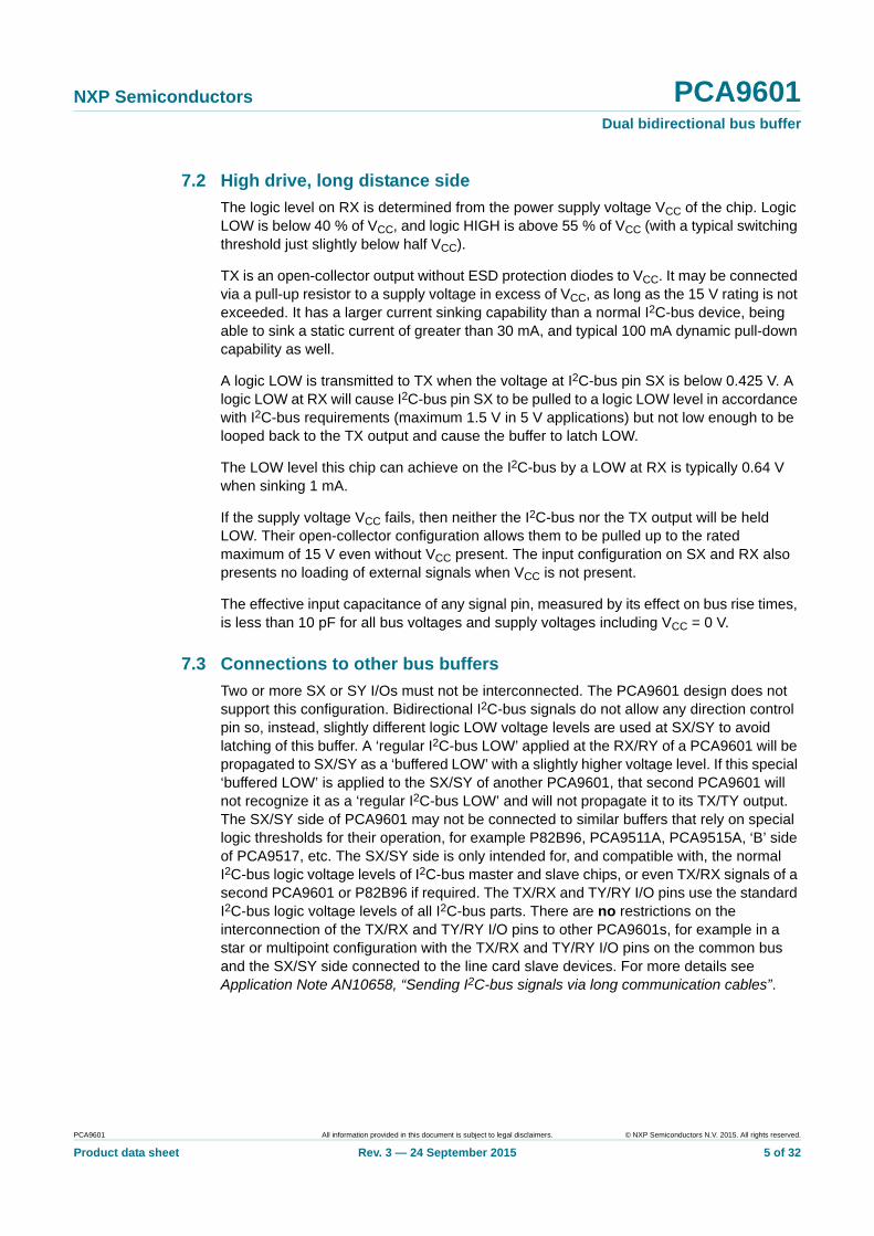
6. Pinning information
6.1 Pinning
6.2 Pin description
Fig 1. Block diagram of PCA9601
PCA9601
SX (SDA)
RX (RxD, SDA)
SY (SCL)
TX (TxD, SDA)
TY (TxD, SCL)
GND
RY (RxD, SCL)
002aae873
VCC (2.5 V to 15 V)
8
1
7
4
3
2
5
6
static level offsetcard side
higher drive,longer distance side
Fig 2. Pin configuration for SO8 Fig 3. Pin configuration for TSSOP8 (MSOP8)
PCA9601D
SX VCC
RX SY
TX RY
GND TY
002aae874
1
2
3
4
6
5
8
7
PCA9601DP
SX VCC
RX SY
TX RY
GND TY
002aae875
1
2
3
4
6
5
8
7
Table 3. Pin description
Symbol Pin Description
SX 1 I2C-bus (SDA or SCL)
RX 2 receive signal
TX 3 transmit signal
GND 4 negative supply voltage
TY 5 transmit signal
RY 6 receive signal
SY 7 I2C-bus (SDA or SCL)
VCC 8 positive supply voltage
PCA9601 All information provided in this document is subject to legal disclaimers. © NXP Semiconductors N.V. 2015. All rights reserved.
Product data sheet Rev. 3 — 24 September 2015 3 of 32

NXP Semiconductors PCA9601Dual bidirectional bus buffer
7. Functional description
Refer to Figure 1 “Block diagram of PCA9601”.
The PCA9601 has two identical buffers allowing buffering of SDA and SCL I2C-bus signals. Each buffer is made up of two logic signal paths, a forward path from the I2C-bus interface, pins SX and SY which drive the buffered bus, and a reverse signal path from the buffered bus input, pins RX and RY to drive the I2C-bus interface. These paths:
• sense the voltage state of I2C-bus pins SX (and SY) and transmit this state to pin TX (and TY respectively), and
• sense the state of pins RX and RY and pull the I2C-bus pin LOW whenever pin RX or pin RY is LOW.
The rest of this discussion will address only the ‘X’ side of the buffer; the ‘Y’ side is identical.
7.1 Static level offset card side
The I2C-bus pin SX is specified to allow interfacing with Fast-mode, Fm+ and TTL-based systems.
The logic threshold voltage levels at SX on this I2C-bus are independent of the IC supply voltage VCC. The maximum I2C-bus supply voltage is 15 V.
7.1.1 Fast-mode operation
When interfacing with Fast-mode systems, the SX pin is guaranteed to sink the normal 3 mA with a VOL of 0.74 V maximum. That guarantees compliance with the Fast-mode I2C-bus specification for all I2C-bus voltages greater than 3 V, as well as compliance with SMBus or other systems that use TTL switching levels.
SX is guaranteed to sink an external 3 mA in addition to its internally sourced pull-up of typically 300 A (maximum 1 mA at 40 C). When selecting the pull-up for the bus at SX, the sink capability of other connected drivers should be taken into account. Most TTL devices are specified to sink at least 4 mA so then the pull-up is limited to 3 mA by the requirement to ensure the 0.8 V TTL LOW.
For Fast-mode I2C-bus operation, the other connected I2C-bus parts may have the minimum sink capability of 3 mA. SX sources typically 300 A (maximum 1 mA at 40 C), which forms part of the external driver loading. When selecting the pull-up it is necessary to subtract the SX pin pull-up current, so, worst-case at 40 C, the allowed pull-up can be limited (by external drivers) to 2 mA.
7.1.2 Fast-mode Plus operation
When the interface at SX is an Fm+ bus with a voltage greater than 4 V, its higher specified sink capability may be used. PCA9601 has a guaranteed sink capability of 15 mA at VOL = 1 V maximum over 0 C to 85 C. That 1 V complies with the bus LOW requirement (0.25Vbus) of any Fm+ bus operating at 4 V or greater. Since the other connected Fm+ devices have a drive capability greater than 20 mA, the pull-up may be selected for 15 mA sink current at VOL = 1 V. For a nominal 5 V bus (5.5 V maximum) the allowed pull-up is (5.5 V 1 V) / 15 mA = 300 . With 300 pull-up, the Fm+ rise time of 120 ns maximum can be met with total bus loading up to 470 pF.
PCA9601 All information provided in this document is subject to legal disclaimers. © NXP Semiconductors N.V. 2015. All rights reserved.
Product data sheet Rev. 3 — 24 September 2015 4 of 32
NXP Semiconductors PCA9601Dual bidirectional bus buffer
7.2 High drive, long distance side
The logic level on RX is determined from the power supply voltage VCC of the chip. Logic LOW is below 40 % of VCC, and logic HIGH is above 55 % of VCC (with a typical switching threshold just slightly below half VCC).
TX is an open-collector output without ESD protection diodes to VCC. It may be connected via a pull-up resistor to a supply voltage in excess of VCC, as long as the 15 V rating is not exceeded. It has a larger current sinking capability than a normal I2C-bus device, being able to sink a static current of greater than 30 mA, and typical 100 mA dynamic pull-down capability as well.
A logic LOW is transmitted to TX when the voltage at I2C-bus pin SX is below 0.425 V. A logic LOW at RX will cause I2C-bus pin SX to be pulled to a logic LOW level in accordance with I2C-bus requirements (maximum 1.5 V in 5 V applications) but not low enough to be looped back to the TX output and cause the buffer to latch LOW.
The LOW level this chip can achieve on the I2C-bus by a LOW at RX is typically 0.64 V when sinking 1 mA.
If the supply voltage VCC fails, then neither the I2C-bus nor the TX output will be held LOW. Their open-collector configuration allows them to be pulled up to the rated maximum of 15 V even without VCC present. The input configuration on SX and RX also presents no loading of external signals when VCC is not present.
The effective input capacitance of any signal pin, measured by its effect on bus rise times, is less than 10 pF for all bus voltages and supply voltages including VCC = 0 V.
7.3 Connections to other bus buffers
Two or more SX or SY I/Os must not be interconnected. The PCA9601 design does not support this configuration. Bidirectional I2C-bus signals do not allow any direction control pin so, instead, slightly different logic LOW voltage levels are used at SX/SY to avoid latching of this buffer. A ‘regular I2C-bus LOW’ applied at the RX/RY of a PCA9601 will be propagated to SX/SY as a ‘buffered LOW’ with a slightly higher voltage level. If this special ‘buffered LOW’ is applied to the SX/SY of another PCA9601, that second PCA9601 will not recognize it as a ‘regular I2C-bus LOW’ and will not propagate it to its TX/TY output. The SX/SY side of PCA9601 may not be connected to similar buffers that rely on special logic thresholds for their operation, for example P82B96, PCA9511A, PCA9515A, ‘B’ side of PCA9517, etc. The SX/SY side is only intended for, and compatible with, the normal I2C-bus logic voltage levels of I2C-bus master and slave chips, or even TX/RX signals of a second PCA9601 or P82B96 if required. The TX/RX and TY/RY I/O pins use the standard I2C-bus logic voltage levels of all I2C-bus parts. There are no restrictions on the interconnection of the TX/RX and TY/RY I/O pins to other PCA9601s, for example in a star or multipoint configuration with the TX/RX and TY/RY I/O pins on the common bus and the SX/SY side connected to the line card slave devices. For more details see Application Note AN10658, “Sending I2C-bus signals via long communication cables”.
PCA9601 All information provided in this document is subject to legal disclaimers. © NXP Semiconductors N.V. 2015. All rights reserved.
Product data sheet Rev. 3 — 24 September 2015 5 of 32
NXP Semiconductors PCA9601Dual bidirectional bus buffer
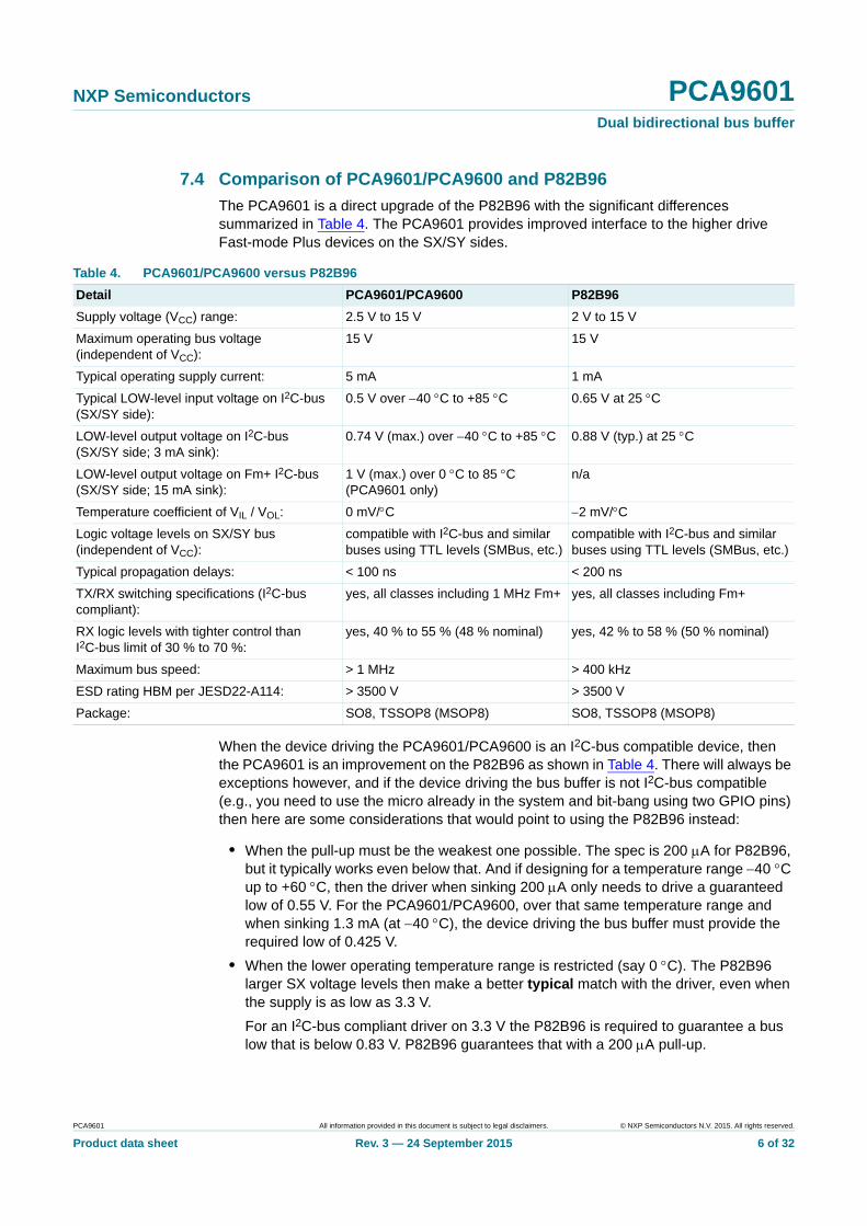
7.4 Comparison of PCA9601/PCA9600 and P82B96
The PCA9601 is a direct upgrade of the P82B96 with the significant differences summarized in Table 4. The PCA9601 provides improved interface to the higher drive Fast-mode Plus devices on the SX/SY sides.
When the device driving the PCA9601/PCA9600 is an I2C-bus compatible device, then the PCA9601 is an improvement on the P82B96 as shown in Table 4. There will always be exceptions however, and if the device driving the bus buffer is not I2C-bus compatible (e.g., you need to use the micro already in the system and bit-bang using two GPIO pins) then here are some considerations that would point to using the P82B96 instead:
• When the pull-up must be the weakest one possible. The spec is 200 A for P82B96, but it typically works even below that. And if designing for a temperature range 40 C up to +60 C, then the driver when sinking 200 A only needs to drive a guaranteed low of 0.55 V. For the PCA9601/PCA9600, over that same temperature range and when sinking 1.3 mA (at 40 C), the device driving the bus buffer must provide the required low of 0.425 V.
• When the lower operating temperature range is restricted (say 0 C). The P82B96 larger SX voltage levels then make a better typical match with the driver, even when the supply is as low as 3.3 V.
For an I2C-bus compliant driver on 3.3 V the P82B96 is required to guarantee a bus low that is below 0.83 V. P82B96 guarantees that with a 200 A pull-up.
Table 4. PCA9601/PCA9600 versus P82B96
Detail PCA9601/PCA9600 P82B96
Supply voltage (VCC) range: 2.5 V to 15 V 2 V to 15 V
Maximum operating bus voltage (independent of VCC):
15 V 15 V
Typical operating supply current: 5 mA 1 mA
Typical LOW-level input voltage on I2C-bus (SX/SY side):
0.5 V over 40 C to +85 C 0.65 V at 25 C
LOW-level output voltage on I2C-bus (SX/SY side; 3 mA sink):
0.74 V (max.) over 40 C to +85 C 0.88 V (typ.) at 25 C
LOW-level output voltage on Fm+ I2C-bus (SX/SY side; 15 mA sink):
1 V (max.) over 0 C to 85 C (PCA9601 only)
n/a
Temperature coefficient of VIL / VOL: 0 mV/C 2 mV/C
Logic voltage levels on SX/SY bus (independent of VCC):
compatible with I2C-bus and similar buses using TTL levels (SMBus, etc.)
compatible with I2C-bus and similar buses using TTL levels (SMBus, etc.)
Typical propagation delays: < 100 ns < 200 ns
TX/RX switching specifications (I2C-bus compliant):
yes, all classes including 1 MHz Fm+ yes, all classes including Fm+
RX logic levels with tighter control than I2C-bus limit of 30 % to 70 %:
yes, 40 % to 55 % (48 % nominal) yes, 42 % to 58 % (50 % nominal)
Maximum bus speed: > 1 MHz > 400 kHz
ESD rating HBM per JESD22-A114: > 3500 V > 3500 V
Package: SO8, TSSOP8 (MSOP8) SO8, TSSOP8 (MSOP8)
PCA9601 All information provided in this document is subject to legal disclaimers. © NXP Semiconductors N.V. 2015. All rights reserved.
Product data sheet Rev. 3 — 24 September 2015 6 of 32
NXP Semiconductors PCA9601Dual bidirectional bus buffer
• When the operating temperature range is restricted at both limits. An I2C driver's typical output is well below 0.4 V and the P82B96 typically requires 0.6 V input even at +60 C, so there is a reasonable margin. The PCA9601/PCA9600 requires a typical input low of 0.5 V so its typical margin is smaller. At 0 C the driver requires a typical input low of 1.16 V and P82B96 provides 0.75 V, so again the typical margin is already quite big and even though PCA9601/PCA9600 is better, providing 0.7 V, that difference is not big.
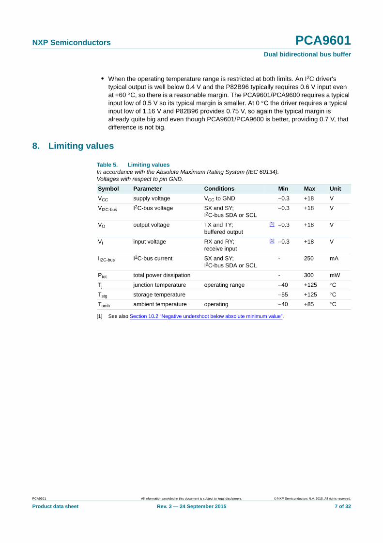
8. Limiting values
[1] See also Section 10.2 “Negative undershoot below absolute minimum value”.
Table 5. Limiting valuesIn accordance with the Absolute Maximum Rating System (IEC 60134).Voltages with respect to pin GND.
Symbol Parameter Conditions Min Max Unit
VCC supply voltage VCC to GND 0.3 +18 V
VI2C-bus I2C-bus voltage SX and SY; I2C-bus SDA or SCL
0.3 +18 V
VO output voltage TX and TY; buffered output
[1] 0.3 +18 V
VI input voltage RX and RY; receive input
[1] 0.3 +18 V
II2C-bus I2C-bus current SX and SY; I2C-bus SDA or SCL
- 250 mA
Ptot total power dissipation - 300 mW
Tj junction temperature operating range 40 +125 C
Tstg storage temperature 55 +125 C
Tamb ambient temperature operating 40 +85 C
PCA9601 All information provided in this document is subject to legal disclaimers. © NXP Semiconductors N.V. 2015. All rights reserved.
Product data sheet Rev. 3 — 24 September 2015 7 of 32

NXP Semiconductors PCA9601Dual bidirectional bus buffer
9. Characteristics
Table 6. CharacteristicsTamb = 40 C to +85 C unless otherwise specified; voltages are specified with respect to GND with VCC = 2.5 V to 15 V unless otherwise specified. Typical values are measured at VCC = 5 V and Tamb = 25 C.
Symbol Parameter Conditions Min Typ Max Unit
Power supply
VCC supply voltage operating 2.5 - 15 V
ICC supply current VCC = 5 V; buses HIGH - 5.2 6.75 mA
VCC = 15 V; buses HIGH - 5.5 7.3 mA
ICC additional supply current per TX/TY output driven LOW; VCC = 5.5 V
- 1.4 3.0 mA
Bus pull-up (load) voltages and currents
Pins SX and SY; I2C-bus
VI input voltage open-collector; RX and RY HIGH - - 15 V
VO output voltage open-collector; RX and RY HIGH - - 15 V
IO output current static; VSX = VSY = 0.4 V [1] 0.3 - 15 mA
IO(sink) output sink current VSX = VSY = 1 V; RX and RY LOW; Tamb = 0 C to 85 C
15 - - mA
IL leakage current VSX = VSY = 15 V; RX and RY HIGH - - 10 A
Pins TX and TY
VO output voltage open-collector - - 15 V
Iload load current maximum recommended on buffered bus; VTX = VTY = 0.4 V; SX and SY LOW on I2C-bus = 0.4 V
- - 30 mA
IO output current from buffered bus; VTX = VTY = 1 V; SX and SY LOW on I2C-bus = 0.4 V
60 130 - mA
IL leakage current on buffered bus; VTX = VTY = VCC = 15 V; SX and SY HIGH
- - 10 A
Input currents
II input current from I2C-bus on SX and SY
RX and RY HIGH or LOW; SX and SY LOW 1 V
[1] - 0.3 1 mA
RX and RY HIGH; SX and SY HIGH > 1.4 V
[1] - - 10 A
from buffered bus on RX and RY; SX and SY HIGH or LOW; VRX = VRY = 0.4 V
[2] - 1.5 10 A
IL leakage current on buffered bus input on RX and RY; VRX = VRY = 15 V
- - 10 A
PCA9601 All information provided in this document is subject to legal disclaimers. © NXP Semiconductors N.V. 2015. All rights reserved.
Product data sheet Rev. 3 — 24 September 2015 8 of 32
NXP Semiconductors PCA9601Dual bidirectional bus buffer
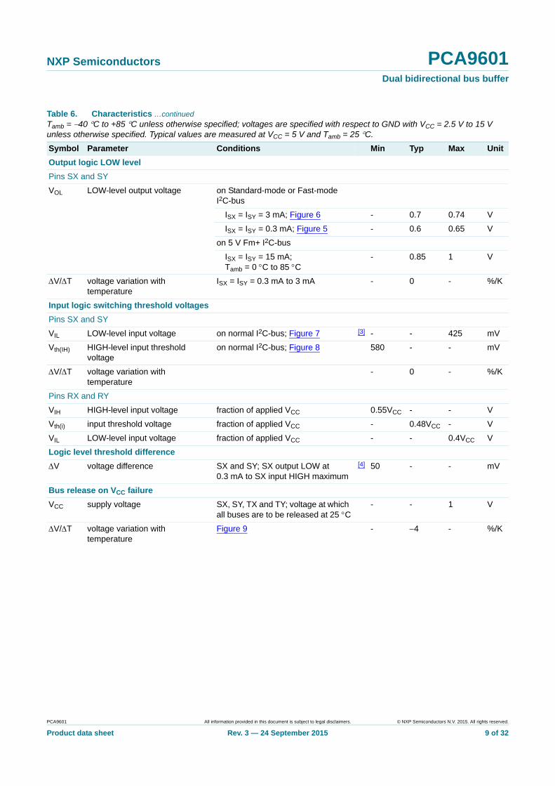
Output logic LOW level
Pins SX and SY
VOL LOW-level output voltage on Standard-mode or Fast-mode I2C-bus
ISX = ISY = 3 mA; Figure 6 - 0.7 0.74 V
ISX = ISY = 0.3 mA; Figure 5 - 0.6 0.65 V
on 5 V Fm+ I2C-bus
ISX = ISY = 15 mA; Tamb = 0 C to 85 C
- 0.85 1 V
V/T voltage variation with temperature
ISX = ISY = 0.3 mA to 3 mA - 0 - %/K
Input logic switching threshold voltages
Pins SX and SY
VIL LOW-level input voltage on normal I2C-bus; Figure 7 [3] - - 425 mV
Vth(IH) HIGH-level input threshold voltage
on normal I2C-bus; Figure 8 580 - - mV
V/T voltage variation with temperature
- 0 - %/K
Pins RX and RY
VIH HIGH-level input voltage fraction of applied VCC 0.55VCC - - V
Vth(i) input threshold voltage fraction of applied VCC - 0.48VCC - V
VIL LOW-level input voltage fraction of applied VCC - - 0.4VCC V
Logic level threshold difference
V voltage difference SX and SY; SX output LOW at 0.3 mA to SX input HIGH maximum
[4] 50 - - mV
Bus release on VCC failure
VCC supply voltage SX, SY, TX and TY; voltage at which all buses are to be released at 25 C
- - 1 V
V/T voltage variation with temperature
Figure 9 - 4 - %/K
Table 6. Characteristics …continuedTamb = 40 C to +85 C unless otherwise specified; voltages are specified with respect to GND with VCC = 2.5 V to 15 V unless otherwise specified. Typical values are measured at VCC = 5 V and Tamb = 25 C.
Symbol Parameter Conditions Min Typ Max Unit
PCA9601 All information provided in this document is subject to legal disclaimers. © NXP Semiconductors N.V. 2015. All rights reserved.
Product data sheet Rev. 3 — 24 September 2015 9 of 32
NXP Semiconductors PCA9601Dual bidirectional bus buffer
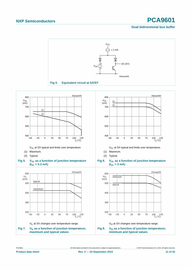
[1] This bus pull-up current specification is intended to assist design of the bus pull-up resistor. It is not a specification of the sink capability (see VOL under sub-section “Output logic LOW level”). When used on an Fm+ bus the load current is limited to 15 mA by the drive capability of PCA9601. When used in a standard I2C-bus the load current is limited by the drive capability of other devices on the bus. The maximum static sink current for a Standard/Fast-mode I2C-bus is 3 mA and PCA9601 is guaranteed to sink more than 3 mA at SX/SY when its pins are holding the bus LOW. However, when an external device pulls the SX/SY pins below 1.4 V, the PCA9601 will source a current between 0 mA and 1 mA maximum. When that other external device is driving LOW it will pull the bus connected to SX or SY down to, or below, the 0.4 V level referenced in the I2C-bus specification and in these test conditions. Then that device must be able to sink up to 1 mA coming from SX/SY plus the usual pull-up current. Therefore in Standard and Fast-mode systems the external pull-up used at SX/SY should be limited to 2 mA. The typical and maximum currents sourced by SX/SY as a function of junction temperature are shown in Figure 10, and the equivalent circuit at the SX/SY interface is shown in Figure 4.
[2] Valid over temperature for VCC 5 V. At higher VCC, this current may increase to maximum 20 A at VCC = 15 V.
[3] The input logic threshold is independent of the supply voltage.
[4] The minimum value requirement for pull-up current, 0.3 mA, guarantees that the minimum value for VSX output LOW will always exceed the maximum VSX input HIGH level to eliminate any possibility of latching. The specified difference is guaranteed by design within any IC. While the tolerances on absolute levels allow a small probability, the LOW from one SX output is recognized by an SX input of another PCA9601, this has no consequences for normal applications. In any design the SX pins of different ICs should never be linked because the resulting system would be very susceptible to induced noise and would not support all I2C-bus operating modes.
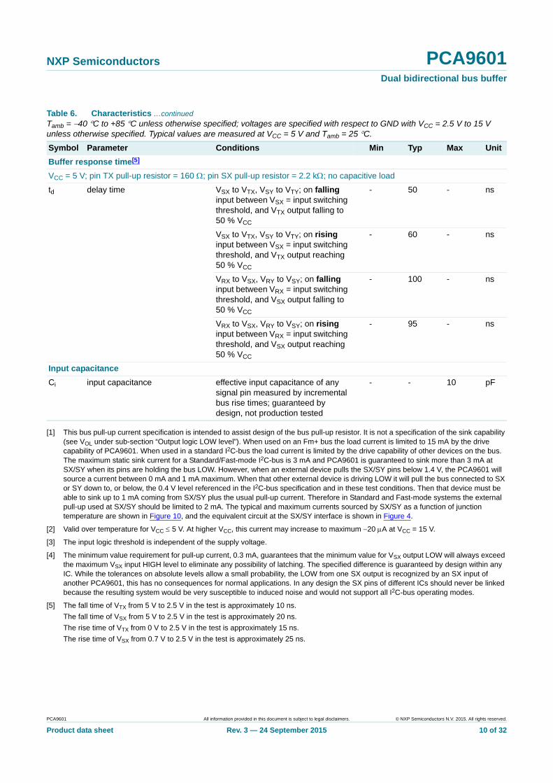
[5] The fall time of VTX from 5 V to 2.5 V in the test is approximately 10 ns.
The fall time of VSX from 5 V to 2.5 V in the test is approximately 20 ns.
The rise time of VTX from 0 V to 2.5 V in the test is approximately 15 ns.
The rise time of VSX from 0.7 V to 2.5 V in the test is approximately 25 ns.
Buffer response time[5]
VCC = 5 V; pin TX pull-up resistor = 160 ; pin SX pull-up resistor = 2.2 k; no capacitive load
td delay time VSX to VTX, VSY to VTY; on falling input between VSX = input switching threshold, and VTX output falling to 50 % VCC
- 50 - ns
VSX to VTX, VSY to VTY; on rising input between VSX = input switching threshold, and VTX output reaching 50 % VCC
- 60 - ns
VRX to VSX, VRY to VSY; on falling input between VRX = input switching threshold, and VSX output falling to 50 % VCC
- 100 - ns
VRX to VSX, VRY to VSY; on rising input between VRX = input switching threshold, and VSX output reaching 50 % VCC
- 95 - ns
Input capacitance
Ci input capacitance effective input capacitance of any signal pin measured by incremental bus rise times; guaranteed by design, not production tested
- - 10 pF
Table 6. Characteristics …continuedTamb = 40 C to +85 C unless otherwise specified; voltages are specified with respect to GND with VCC = 2.5 V to 15 V unless otherwise specified. Typical values are measured at VCC = 5 V and Tamb = 25 C.
Symbol Parameter Conditions Min Typ Max Unit
PCA9601 All information provided in this document is subject to legal disclaimers. © NXP Semiconductors N.V. 2015. All rights reserved.
Product data sheet Rev. 3 — 24 September 2015 10 of 32
NXP Semiconductors PCA9601Dual bidirectional bus buffer
Fig 4. Equivalent circuit at SX/SY
002aac838
VCC
≤ 1 mA
SX (SY)Vref
VOL at SX typical and limits over temperature.
(1) Maximum.
(2) Typical.
VOL at SX typical and limits over temperature.
(1) Maximum.
(2) Typical.
Fig 5. VOL as a function of junction temperature (IOL = 0.3 mA)
Fig 6. VOL as a function of junction temperature (IOL = 3 mA)
VIL at SX changes over temperature range. VIH at SX changes over temperature range.
Fig 7. VIL as a function of junction temperature; maximum and typical values
Fig 8. VIH as a function of junction temperature; minimum and typical values
800VOL(mV)
400
Tj (°C)
002aac839
(1)
−50 1251007550250−25
(2)600
500
700
800VOL(mV)
400
Tj (°C)
002aac840
(1)
−50 1251007550250−25
(2)
600
500
700
600VIL
(mV)
200
Tj (°C)
002aag005
500
400
300
−50 1251007550250−25
maximum
typical
600VIH
(mV)
200
Tj (°C)
002aag006
500
400
300
−50 1251007550250−25
minimum
typical
PCA9601 All information provided in this document is subject to legal disclaimers. © NXP Semiconductors N.V. 2015. All rights reserved.
Product data sheet Rev. 3 — 24 September 2015 11 of 32
NXP Semiconductors PCA9601Dual bidirectional bus buffer
(1) Maximum.
(2) Typical.
Fig 9. VCC bus release limit over temperature; maximum values
Fig 10. Current sourced out of SX/SY as a function of junction temperature if these pins are externally pulled to 0.4 V or lower
Fig 11. Typical SX/SY current versus LOW-level output voltage
600
1400VCC(max)
(mV)
400
Tj (°C)
002aac075
−50 1251007550250−25
800
1000
1200
200
1000II
(μA)
0
Tj (°C)
001aai062
−50 1251007550250−25
400
600
800(1)
(2)
002aaf484
ISX, ISY (mA)0 302010
0
1.0
0.6
0.4
1.4VOL(V)
0.2
0.8
1.2
PCA9601 All information provided in this document is subject to legal disclaimers. © NXP Semiconductors N.V. 2015. All rights reserved.
Product data sheet Rev. 3 — 24 September 2015 12 of 32
NXP Semiconductors PCA9601Dual bidirectional bus buffer
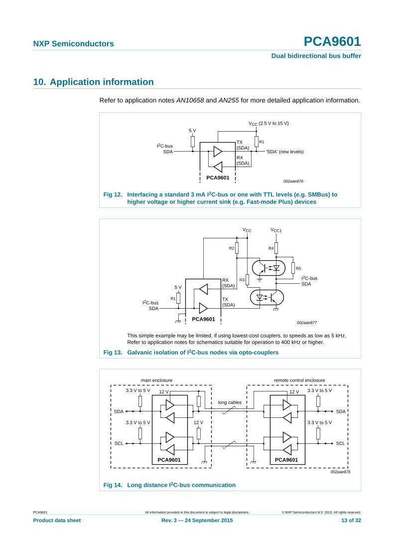
10. Application information
Refer to application notes AN10658 and AN255 for more detailed application information.
Fig 12. Interfacing a standard 3 mA I2C-bus or one with TTL levels (e.g. SMBus) to higher voltage or higher current sink (e.g. Fast-mode Plus) devices
This simple example may be limited, if using lowest-cost couplers, to speeds as low as 5 kHz. Refer to application notes for schematics suitable for operation to 400 kHz or higher.
Fig 13. Galvanic isolation of I2C-bus nodes via opto-couplers
Fig 14. Long distance I2C-bus communication
PCA9601
I2C-busSDA
002aae876
5 V
VCC (2.5 V to 15 V)
R1
RX(SDA)
TX(SDA)
'SDA' (new levels)
PCA9601
I2C-busSDA
002aae877
5 V
R1
VCC
R2
R3RX(SDA)
TX(SDA)
R5
R4
VCC1
I2C-busSDA
PCA9601
SDA
SCL
002aae878
12 V
12 V3.3 V to 5 V
3.3 V to 5 V
long cables
main enclosure
PCA9601
SDA
SCL
3.3 V to 5 V
3.3 V to 5 V
remote control enclosure
12 V
PCA9601 All information provided in this document is subject to legal disclaimers. © NXP Semiconductors N.V. 2015. All rights reserved.
Product data sheet Rev. 3 — 24 September 2015 13 of 32
NXP Semiconductors PCA9601Dual bidirectional bus buffer
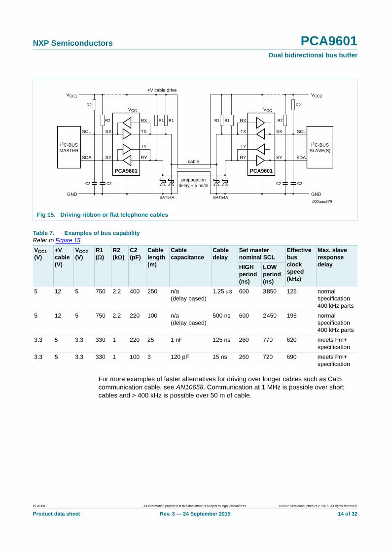
For more examples of faster alternatives for driving over longer cables such as Cat5 communication cable, see AN10658. Communication at 1 MHz is possible over short cables and > 400 kHz is possible over 50 m of cable.
Fig 15. Driving ribbon or flat telephone cables
PCA9601
SCL
RX
TX
002aae879
SX
VCC
TY
RYSY
R2
R2
C2C2
I2C-BUSMASTER
SDA
VCC1
GND
R1 R1
BAT54A
cable
propagationdelay ≈ 5 ns/m
BAT54A
R1 R1
PCA9601
RX
TX
TY
RY
VCC
SX
SY
R2
R2
SCL
SDA
VCC2
GND
I2C-BUSSLAVE(S)
C2C2
+V cable drive
Table 7. Examples of bus capabilityRefer to Figure 15.
VCC1 (V)
+V cable (V)
VCC2 (V)
R1 ()
R2 (k)
C2 (pF)
Cable length (m)
Cable capacitance
Cable delay
Set master nominal SCL
Effective bus clock speed (kHz)
Max. slave response delayHIGH
period (ns)
LOW period (ns)
5 12 5 750 2.2 400 250 n/a (delay based)
1.25 s 600 3850 125 normal specification 400 kHz parts
5 12 5 750 2.2 220 100 n/a (delay based)
500 ns 600 2450 195 normal specification 400 kHz parts
3.3 5 3.3 330 1 220 25 1 nF 125 ns 260 770 620 meets Fm+ specification
3.3 5 3.3 330 1 100 3 120 pF 15 ns 260 720 690 meets Fm+ specification
PCA9601 All information provided in this document is subject to legal disclaimers. © NXP Semiconductors N.V. 2015. All rights reserved.
Product data sheet Rev. 3 — 24 September 2015 14 of 32

NXP Semiconductors PCA9601Dual bidirectional bus buffer
10.1 Calculating system delays and bus clock frequency
Effective delay of SCL at slave: 120 + 17VCCM + (2.5 + 4 109 Cb) VCCB + 10VCCS (ns).
C = F; V = V.
Fig 16. Falling edge of SCL at master is delayed by the buffers and bus fall times
PCA9601 PCA9601
SCL
SX
local master bus
VCCM
SCLMASTER
I2C-BUSCsslave buscapacitance
Cbbuffered buswiring capacitance
Cmmaster buscapacitance
Rm
GND (0 V)
VCCB
buffered expansion bus
TX/RX TX/RX SX
Rb Rs
I2C-BUS
SLAVE
VCCS
remote slave bus
002aae880
Effective delay of SCL at master: 115 + (Rm Cm) + (0.7 Rb Cb) (ns).
C = F; R = .
Fig 17. Rising edge of SCL at master is delayed (clock stretch) by buffer and bus rise times
PCA9601SX
local master bus
VCCM
SCLMASTER
I2C-BUSCbbuffered buswiring capacitance
Cmmaster buscapacitance
Rm
GND (0 V)
VCCB
buffered expansion bus
TX/RXTX/RX
Rb
002aae881
PCA9601 All information provided in this document is subject to legal disclaimers. © NXP Semiconductors N.V. 2015. All rights reserved.
Product data sheet Rev. 3 — 24 September 2015 15 of 32
NXP Semiconductors PCA9601Dual bidirectional bus buffer
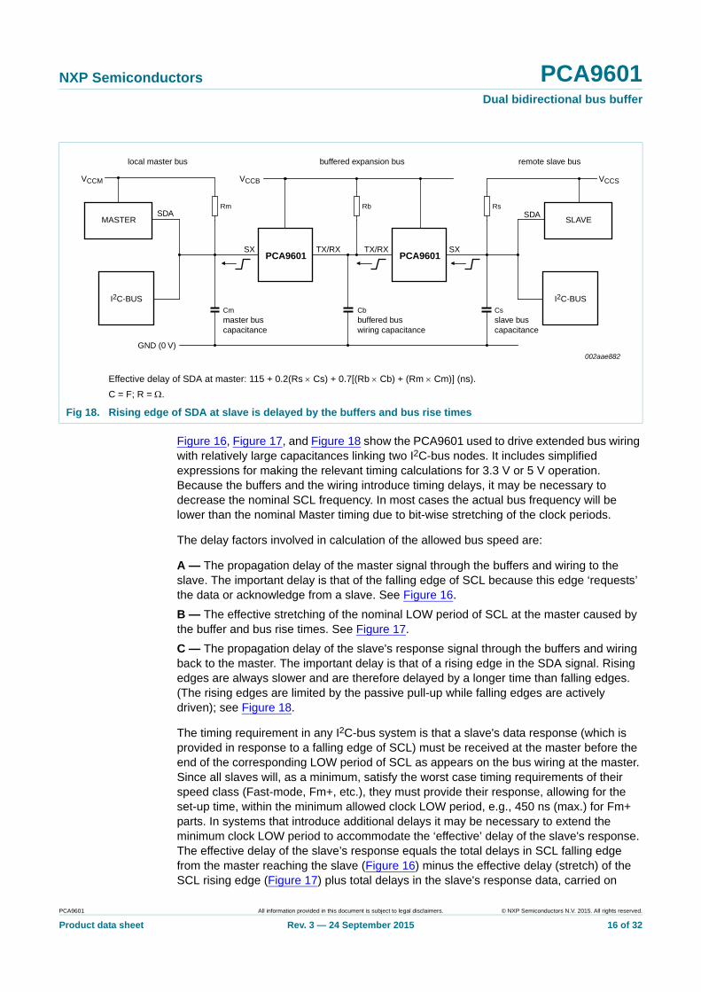
Figure 16, Figure 17, and Figure 18 show the PCA9601 used to drive extended bus wiring with relatively large capacitances linking two I2C-bus nodes. It includes simplified expressions for making the relevant timing calculations for 3.3 V or 5 V operation. Because the buffers and the wiring introduce timing delays, it may be necessary to decrease the nominal SCL frequency. In most cases the actual bus frequency will be lower than the nominal Master timing due to bit-wise stretching of the clock periods.
The delay factors involved in calculation of the allowed bus speed are:
A — The propagation delay of the master signal through the buffers and wiring to the slave. The important delay is that of the falling edge of SCL because this edge ‘requests’ the data or acknowledge from a slave. See Figure 16.
B — The effective stretching of the nominal LOW period of SCL at the master caused by the buffer and bus rise times. See Figure 17.
C — The propagation delay of the slave's response signal through the buffers and wiring back to the master. The important delay is that of a rising edge in the SDA signal. Rising edges are always slower and are therefore delayed by a longer time than falling edges. (The rising edges are limited by the passive pull-up while falling edges are actively driven); see Figure 18.
The timing requirement in any I2C-bus system is that a slave's data response (which is provided in response to a falling edge of SCL) must be received at the master before the end of the corresponding LOW period of SCL as appears on the bus wiring at the master. Since all slaves will, as a minimum, satisfy the worst case timing requirements of their speed class (Fast-mode, Fm+, etc.), they must provide their response, allowing for the set-up time, within the minimum allowed clock LOW period, e.g., 450 ns (max.) for Fm+ parts. In systems that introduce additional delays it may be necessary to extend the minimum clock LOW period to accommodate the ‘effective’ delay of the slave's response. The effective delay of the slave’s response equals the total delays in SCL falling edge from the master reaching the slave (Figure 16) minus the effective delay (stretch) of the SCL rising edge (Figure 17) plus total delays in the slave's response data, carried on
Effective delay of SDA at master: 115 + 0.2(Rs Cs) + 0.7[(Rb Cb) + (Rm Cm)] (ns).
C = F; R = .
Fig 18. Rising edge of SDA at slave is delayed by the buffers and bus rise times
PCA9601 PCA9601
SDA
SX
local master bus
VCCM
SDAMASTER
I2C-BUSCsslave buscapacitance
Cbbuffered buswiring capacitance
Cmmaster buscapacitance
Rm
GND (0 V)
VCCB
buffered expansion bus
TX/RX TX/RX SX
Rb Rs
I2C-BUS
SLAVE
VCCS
remote slave bus
002aae882
PCA9601 All information provided in this document is subject to legal disclaimers. © NXP Semiconductors N.V. 2015. All rights reserved.
Product data sheet Rev. 3 — 24 September 2015 16 of 32
NXP Semiconductors PCA9601Dual bidirectional bus buffer
SDA, reaching the master (Figure 18).
The master microcontroller should be programmed to produce a nominal SCL LOW period as follows:
(1)
The actual LOW period will become (the programmed value + the stretching time B). When this actual LOW period is then less than the specified minimum, the specified minimum should be used.
Example 1:
It is required to connect an Fm+ slave, with Rs Cs product of 100 ns, to a 5 V Fast-mode system also having 100 ns Rm Cm using two PCA9601’s to buffer a 5 V bus with 4 nF loading and 160 pull-up.
Calculate the allowed bus speed:
Delay A = 120 + 85 + (2.5 + [4 4]) 5 + 50 = 347.5 ns
Delay B = 115 + 100 + 70 = 285 ns
Delay C = 115 + 20 + 0.7(100 + 100) = 275 ns
The maximum Fm+ slave response delay must be < 450 ns so the programmed LOW period is calculated as:
LOW 450 + 347.5 285 + 275 + 100 = 887.5 ns
The actual LOW period will be 887.5 + 285 = 1173 ns, which is below the Fast-mode minimum, so the programmed LOW period must be increased to (1300 285) = 1015 ns, so the actual LOW equals the 1300 ns requirement and this shows that this Fast-mode system may be safely run to its limit of 400 kHz.
Example 2:
It is required to buffer a Master with Fm+ speed capability, but only 3 mA sink capability, to an Fm+ bus. All the system operates at 3.3 V. The Master Rm Cm product is 50 ns. Only one PCA9601 is used. The Fm+ bus becomes the buffered bus. The Fm+ bus has 200 pF loading and 150 pull-up, so its Rb Cb product is 30 ns. The Fm+ slave has a specified data valid time tVD;DAT maximum of 300 ns.
Calculate the allowed maximum system bus speed. (Note that the fixed values in the delay equations represent the internal propagation delays of the PCA9601. Only one PCA9601 is used here, so those fixed values used below are taken from the characteristics.)
The delays are:
Delay A = 40 + 56 + (2.5 + [4 0.2]) 3.3 = 107 ns
Delay B = 115 + 50 + 21 = 186 ns
Delay C = 70 + 0.7(50 + 30) = 126 ns
The programmed LOW period is calculated as:
SCL LOW 300 + 117 186 + 126 + 50 = 407 ns
The actual LOW period will be 407 + 126 = 533 ns, which exceeds the minimum Fm+ 500 ns requirement. This system requires the bus LOW period, and therefore cycle time, to be increased by 33 ns so the system must run slightly below the 1 MHz limit.
SCL LOW slave response delay to valid data on its SDA A B C data set-up time+ +–+ ns
PCA9601 All information provided in this document is subject to legal disclaimers. © NXP Semiconductors N.V. 2015. All rights reserved.
Product data sheet Rev. 3 — 24 September 2015 17 of 32
NXP Semiconductors PCA9601Dual bidirectional bus buffer
The possible maximum speed has a cycle period of 1033 ns or 968 kHz.
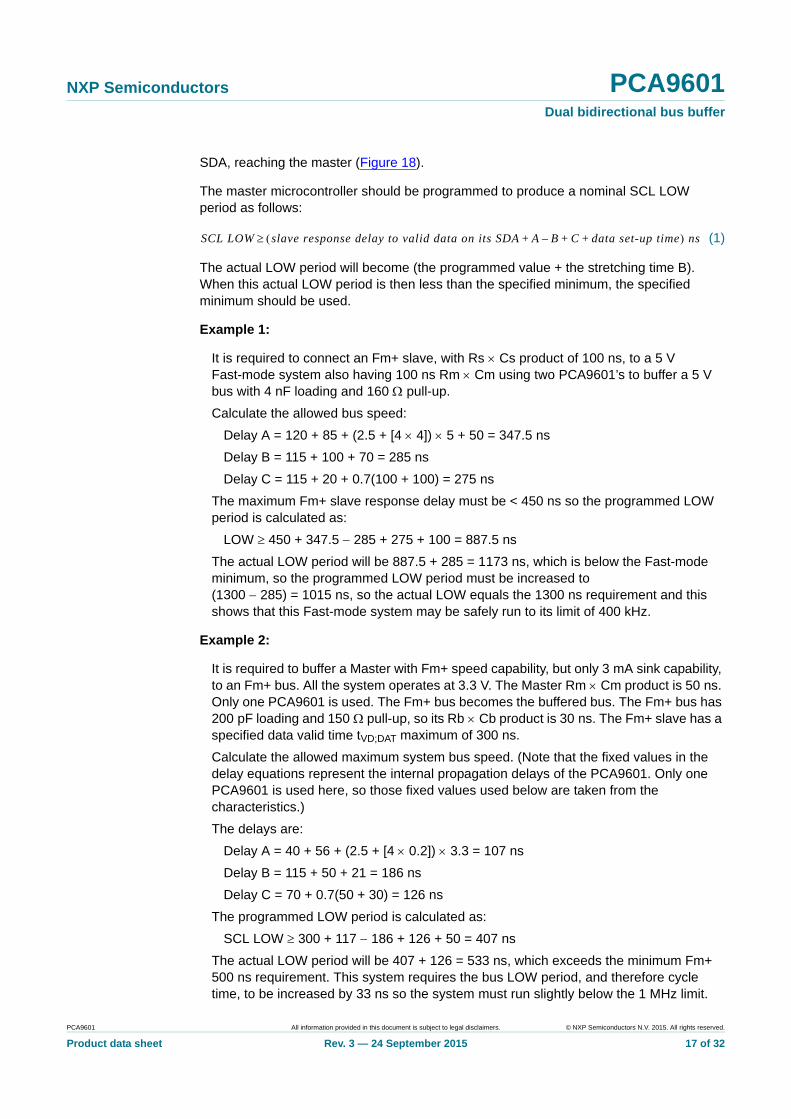
There is an Excel calculator which makes it easy to determine the maximum I2C-bus clock speed when using the PCA9601. The calculator and instructions can be found at www.nxp.com/clockspeedcalculator.
Fig 19. I2C-bus multipoint application
PCA9601
SDARX
SCL
TX
TY
RY
002aae883
12 V
SX
SY
12 V
12 V3.3 V to 5 V
3.3 V to 5 V
PCA9601
SX SY
SCL/SDA
PCA9601
SX SY
SCL/SDA
PCA9601
SX SY
SCL/SDA
PCA9601
SX SCL
SY SDA
no limit to the number of connected bus devices
twisted-pair telephone wires,USB, or flat ribbon cables; up to 15 V logic levels, include VCC and GND
3.3 V 3.3 V
PCA9601 All information provided in this document is subject to legal disclaimers. © NXP Semiconductors N.V. 2015. All rights reserved.
Product data sheet Rev. 3 — 24 September 2015 18 of 32
NXP Semiconductors PCA9601Dual bidirectional bus buffer
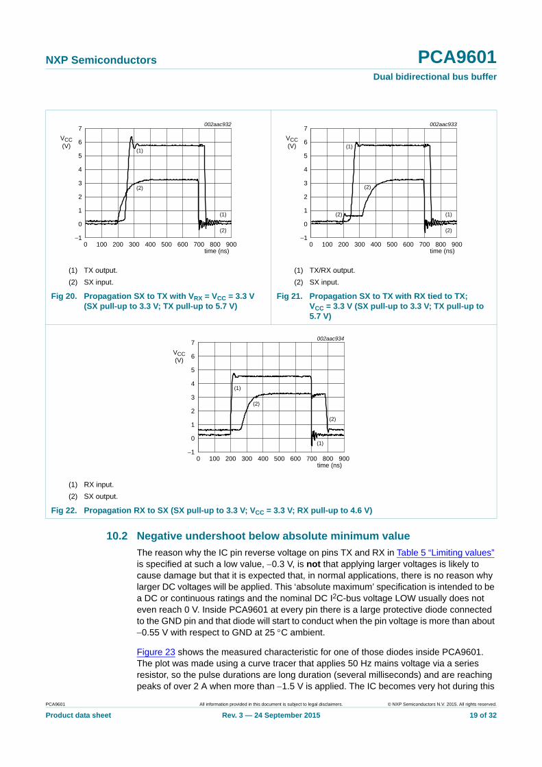
10.2 Negative undershoot below absolute minimum value
The reason why the IC pin reverse voltage on pins TX and RX in Table 5 “Limiting values” is specified at such a low value, 0.3 V, is not that applying larger voltages is likely to cause damage but that it is expected that, in normal applications, there is no reason why larger DC voltages will be applied. This ‘absolute maximum’ specification is intended to be a DC or continuous ratings and the nominal DC I2C-bus voltage LOW usually does not even reach 0 V. Inside PCA9601 at every pin there is a large protective diode connected to the GND pin and that diode will start to conduct when the pin voltage is more than about 0.55 V with respect to GND at 25 C ambient.
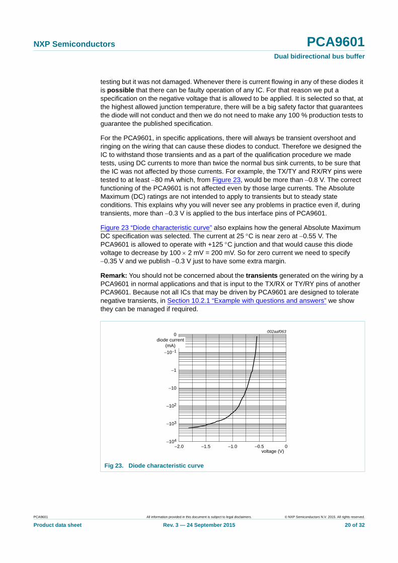
Figure 23 shows the measured characteristic for one of those diodes inside PCA9601. The plot was made using a curve tracer that applies 50 Hz mains voltage via a series resistor, so the pulse durations are long duration (several milliseconds) and are reaching peaks of over 2 A when more than 1.5 V is applied. The IC becomes very hot during this
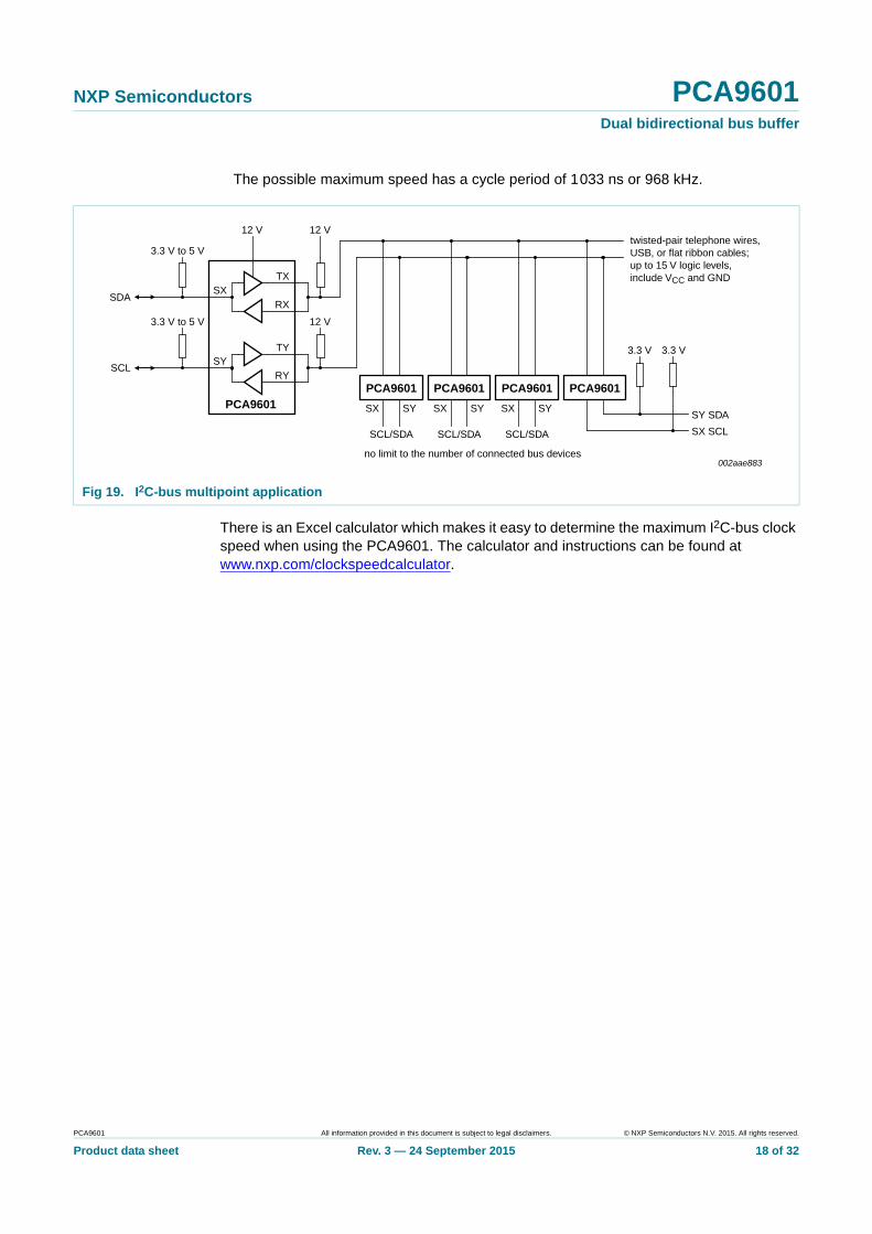
(1) TX output.
(2) SX input.
(1) TX/RX output.
(2) SX input.
Fig 20. Propagation SX to TX with VRX = VCC = 3.3 V (SX pull-up to 3.3 V; TX pull-up to 5.7 V)
Fig 21. Propagation SX to TX with RX tied to TX; VCC = 3.3 V (SX pull-up to 3.3 V; TX pull-up to 5.7 V)
(1) RX input.
(2) SX output.
Fig 22. Propagation RX to SX (SX pull-up to 3.3 V; VCC = 3.3 V; RX pull-up to 4.6 V)
−1
5
3
1
7
VCC(V)
time (ns)0 900
002aac932
200100 300 400 500 600 700 800
0
2
4
6(1)
(2)
(1)
(2)−1
5
3
1
7
VCC(V)
time (ns)0 900
002aac933
200100 300 400 500 600 700 800
0
2
4
6(1)
(2)
(1)
(2)
(2)
−1
5
3
1
7
VCC(V)
time (ns)0 900
002aac934
200100 300 400 500 600 700 800
0
2
4
6
(1)
(2)
(1)
(2)
PCA9601 All information provided in this document is subject to legal disclaimers. © NXP Semiconductors N.V. 2015. All rights reserved.
Product data sheet Rev. 3 — 24 September 2015 19 of 32
NXP Semiconductors PCA9601Dual bidirectional bus buffer
testing but it was not damaged. Whenever there is current flowing in any of these diodes it is possible that there can be faulty operation of any IC. For that reason we put a specification on the negative voltage that is allowed to be applied. It is selected so that, at the highest allowed junction temperature, there will be a big safety factor that guarantees the diode will not conduct and then we do not need to make any 100 % production tests to guarantee the published specification.
For the PCA9601, in specific applications, there will always be transient overshoot and ringing on the wiring that can cause these diodes to conduct. Therefore we designed the IC to withstand those transients and as a part of the qualification procedure we made tests, using DC currents to more than twice the normal bus sink currents, to be sure that the IC was not affected by those currents. For example, the TX/TY and RX/RY pins were tested to at least 80 mA which, from Figure 23, would be more than 0.8 V. The correct functioning of the PCA9601 is not affected even by those large currents. The Absolute Maximum (DC) ratings are not intended to apply to transients but to steady state conditions. This explains why you will never see any problems in practice even if, during transients, more than 0.3 V is applied to the bus interface pins of PCA9601.
Figure 23 “Diode characteristic curve” also explains how the general Absolute Maximum DC specification was selected. The current at 25 C is near zero at 0.55 V. The PCA9601 is allowed to operate with +125 C junction and that would cause this diode voltage to decrease by 100 2 mV = 200 mV. So for zero current we need to specify 0.35 V and we publish 0.3 V just to have some extra margin.
Remark: You should not be concerned about the transients generated on the wiring by a PCA9601 in normal applications and that is input to the TX/RX or TY/RY pins of another PCA9601. Because not all ICs that may be driven by PCA9601 are designed to tolerate negative transients, in Section 10.2.1 “Example with questions and answers” we show they can be managed if required.
Fig 23. Diode characteristic curve
002aaf063
voltage (V)−2.0 0−0.5−1.5 −1.0
−10
−103
−102
−10−1
−1
0
−104
diode current(mA)
PCA9601 All information provided in this document is subject to legal disclaimers. © NXP Semiconductors N.V. 2015. All rights reserved.
Product data sheet Rev. 3 — 24 September 2015 20 of 32
NXP Semiconductors PCA9601Dual bidirectional bus buffer
10.2.1 Example with questions and answers
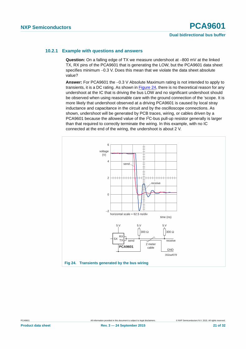
Question: On a falling edge of TX we measure undershoot at 800 mV at the linked TX, RX pins of the PCA9601 that is generating the LOW, but the PCA9601 data sheet specifies minimum 0.3 V. Does this mean that we violate the data sheet absolute value?
Answer: For PCA9601 the 0.3 V Absolute Maximum rating is not intended to apply to transients, it is a DC rating. As shown in Figure 24, there is no theoretical reason for any undershoot at the IC that is driving the bus LOW and no significant undershoot should be observed when using reasonable care with the ground connection of the ‘scope. It is more likely that undershoot observed at a driving PCA9601 is caused by local stray inductance and capacitance in the circuit and by the oscilloscope connections. As shown, undershoot will be generated by PCB traces, wiring, or cables driven by a PCA9601 because the allowed value of the I2C-bus pull-up resistor generally is larger than that required to correctly terminate the wiring. In this example, with no IC connected at the end of the wiring, the undershoot is about 2 V.
Fig 24. Transients generated by the bus wiring
002aaf078
time (ns)
2
0
4
6
voltage(V)
−2horizontal scale = 62.5 ns/div
send
receive
5 V
RXTXSX
PCA9601
send
300 Ω
5 V
2 metercable
5 V
300 Ω
GND
receive
PCA9601 All information provided in this document is subject to legal disclaimers. © NXP Semiconductors N.V. 2015. All rights reserved.
Product data sheet Rev. 3 — 24 September 2015 21 of 32
NXP Semiconductors PCA9601Dual bidirectional bus buffer
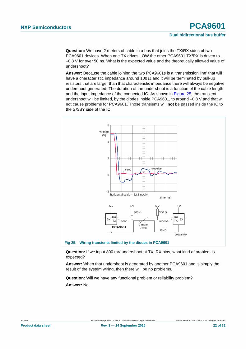
Question: We have 2 meters of cable in a bus that joins the TX/RX sides of two PCA9601 devices. When one TX drives LOW the other PCA9601 TX/RX is driven to 0.8 V for over 50 ns. What is the expected value and the theoretically allowed value of undershoot?
Answer: Because the cable joining the two PCA9601s is a ‘transmission line’ that will have a characteristic impedance around 100 and it will be terminated by pull-up resistors that are larger than that characteristic impedance there will always be negative undershoot generated. The duration of the undershoot is a function of the cable length and the input impedance of the connected IC. As shown in Figure 25, the transient undershoot will be limited, by the diodes inside PCA9601, to around 0.8 V and that will not cause problems for PCA9601. Those transients will not be passed inside the IC to the SX/SY side of the IC.
Question: If we input 800 mV undershoot at TX, RX pins, what kind of problem is expected?
Answer: When that undershoot is generated by another PCA9601 and is simply the result of the system wiring, then there will be no problems.
Question: Will we have any functional problem or reliability problem?
Answer: No.
Fig 25. Wiring transients limited by the diodes in PCA9601
002aaf079
time (ns)
2
0
4
6
voltage(V)
−2horizontal scale = 62.5 ns/div
send receive
5 V
RXTXSX
PCA9601
send
300 Ω
5 V
2 metercable
5 V
300 Ω
GND
receiveSX
RXTX
5 V
PCA9601 All information provided in this document is subject to legal disclaimers. © NXP Semiconductors N.V. 2015. All rights reserved.
Product data sheet Rev. 3 — 24 September 2015 22 of 32
NXP Semiconductors PCA9601Dual bidirectional bus buffer
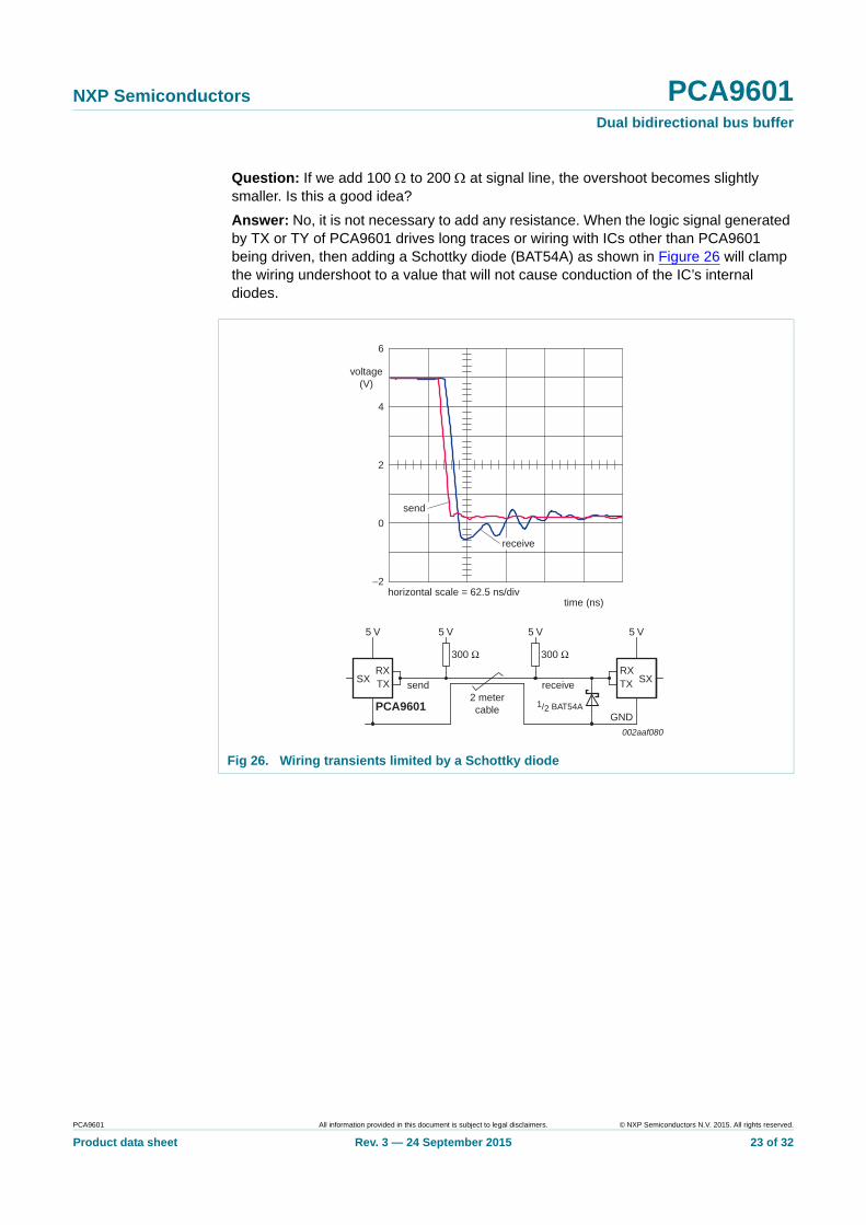
Question: If we add 100 to 200 at signal line, the overshoot becomes slightly smaller. Is this a good idea?
Answer: No, it is not necessary to add any resistance. When the logic signal generated by TX or TY of PCA9601 drives long traces or wiring with ICs other than PCA9601 being driven, then adding a Schottky diode (BAT54A) as shown in Figure 26 will clamp the wiring undershoot to a value that will not cause conduction of the IC’s internal diodes.
Fig 26. Wiring transients limited by a Schottky diode
002aaf080
time (ns)
2
0
4
6
voltage(V)
−2horizontal scale = 62.5 ns/div
receive
5 V
RXTXSX
PCA9601
send
300 Ω
5 V
2 metercable
5 V
300 Ω
GND
receiveSX
RXTX
5 V
send
1/2 BAT54A
PCA9601 All information provided in this document is subject to legal disclaimers. © NXP Semiconductors N.V. 2015. All rights reserved.
Product data sheet Rev. 3 — 24 September 2015 23 of 32
NXP Semiconductors PCA9601Dual bidirectional bus buffer
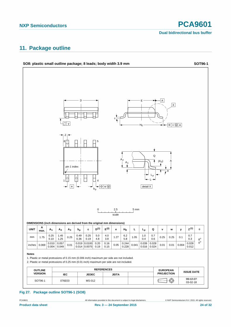
11. Package outline
Fig 27. Package outline SOT96-1 (SO8)
UNITA
max. A1 A2 A3 bp c D(1) E(2) (1)e HE L Lp Q Zywv θ
REFERENCESOUTLINEVERSION
EUROPEANPROJECTION ISSUE DATE
IEC JEDEC JEITA
mm
inches
1.750.250.10
1.451.25
0.250.490.36
0.250.19
5.04.8
4.03.8
1.276.25.8
1.050.70.6
0.70.3 8
0
o
o
0.25 0.10.25
DIMENSIONS (inch dimensions are derived from the original mm dimensions)
Notes
1. Plastic or metal protrusions of 0.15 mm (0.006 inch) maximum per side are not included.
2. Plastic or metal protrusions of 0.25 mm (0.01 inch) maximum per side are not included.
1.00.4
SOT96-1
X
w M
θ
AA1
A2
bp
D
HE
Lp
Q
detail X
E
Z
e
c
L
v M A
(A )3
A
4
5
pin 1 index
1
8
y
076E03 MS-012
0.0690.0100.004
0.0570.049
0.010.0190.014
0.01000.0075
0.200.19
0.160.15
0.050.2440.228
0.0280.024
0.0280.012
0.010.010.041 0.0040.0390.016
0 2.5 5 mm
scale
SO8: plastic small outline package; 8 leads; body width 3.9 mm SOT96-1
99-12-2703-02-18
PCA9601 All information provided in this document is subject to legal disclaimers. © NXP Semiconductors N.V. 2015. All rights reserved.
Product data sheet Rev. 3 — 24 September 2015 24 of 32
NXP Semiconductors PCA9601Dual bidirectional bus buffer
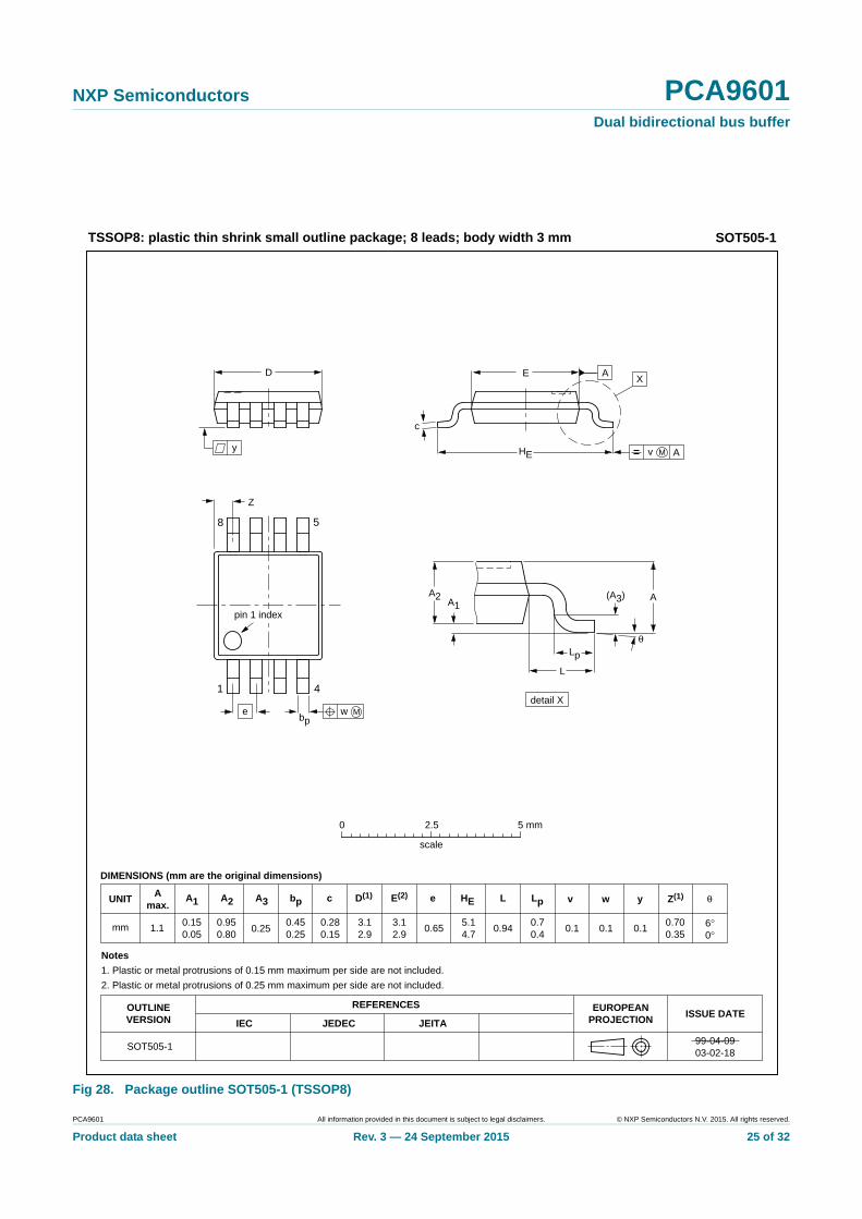
Fig 28. Package outline SOT505-1 (TSSOP8)
UNIT A1A
max.A2 A3 bp LHE Lp w yvc eD(1) E(2) Z(1) θ
REFERENCESOUTLINEVERSION
EUROPEANPROJECTION ISSUE DATE
IEC JEDEC JEITA
mm 0.150.05
0.950.80
0.450.25
0.280.15
3.12.9
3.12.9
0.655.14.7
0.700.35
6°0°
0.1 0.10.10.94
DIMENSIONS (mm are the original dimensions)
Notes
1. Plastic or metal protrusions of 0.15 mm maximum per side are not included.
2. Plastic or metal protrusions of 0.25 mm maximum per side are not included.
0.70.4
SOT505-1 99-04-0903-02-18
w Mbp
D
Z
e
0.25
1 4
8 5
θ
AA2A1
Lp
(A3)
detail X
L
HE
E
c
v M A
XA
y
2.5 5 mm0
scale
TSSOP8: plastic thin shrink small outline package; 8 leads; body width 3 mm SOT505-1
1.1
pin 1 index
PCA9601 All information provided in this document is subject to legal disclaimers. © NXP Semiconductors N.V. 2015. All rights reserved.
Product data sheet Rev. 3 — 24 September 2015 25 of 32
NXP Semiconductors PCA9601Dual bidirectional bus buffer
12. Soldering of SMD packages
This text provides a very brief insight into a complex technology. A more in-depth account of soldering ICs can be found in Application Note AN10365 “Surface mount reflow soldering description”.
12.1 Introduction to soldering
Soldering is one of the most common methods through which packages are attached to Printed Circuit Boards (PCBs), to form electrical circuits. The soldered joint provides both the mechanical and the electrical connection. There is no single soldering method that is ideal for all IC packages. Wave soldering is often preferred when through-hole and Surface Mount Devices (SMDs) are mixed on one printed wiring board; however, it is not suitable for fine pitch SMDs. Reflow soldering is ideal for the small pitches and high densities that come with increased miniaturization.
12.2 Wave and reflow soldering
Wave soldering is a joining technology in which the joints are made by solder coming from a standing wave of liquid solder. The wave soldering process is suitable for the following:
• Through-hole components
• Leaded or leadless SMDs, which are glued to the surface of the printed circuit board
Not all SMDs can be wave soldered. Packages with solder balls, and some leadless packages which have solder lands underneath the body, cannot be wave soldered. Also, leaded SMDs with leads having a pitch smaller than ~0.6 mm cannot be wave soldered, due to an increased probability of bridging.
The reflow soldering process involves applying solder paste to a board, followed by component placement and exposure to a temperature profile. Leaded packages, packages with solder balls, and leadless packages are all reflow solderable.
Key characteristics in both wave and reflow soldering are:
• Board specifications, including the board finish, solder masks and vias
• Package footprints, including solder thieves and orientation
• The moisture sensitivity level of the packages
• Package placement
• Inspection and repair
• Lead-free soldering versus SnPb soldering
12.3 Wave soldering
Key characteristics in wave soldering are:
• Process issues, such as application of adhesive and flux, clinching of leads, board transport, the solder wave parameters, and the time during which components are exposed to the wave
• Solder bath specifications, including temperature and impurities
PCA9601 All information provided in this document is subject to legal disclaimers. © NXP Semiconductors N.V. 2015. All rights reserved.
Product data sheet Rev. 3 — 24 September 2015 26 of 32
NXP Semiconductors PCA9601Dual bidirectional bus buffer
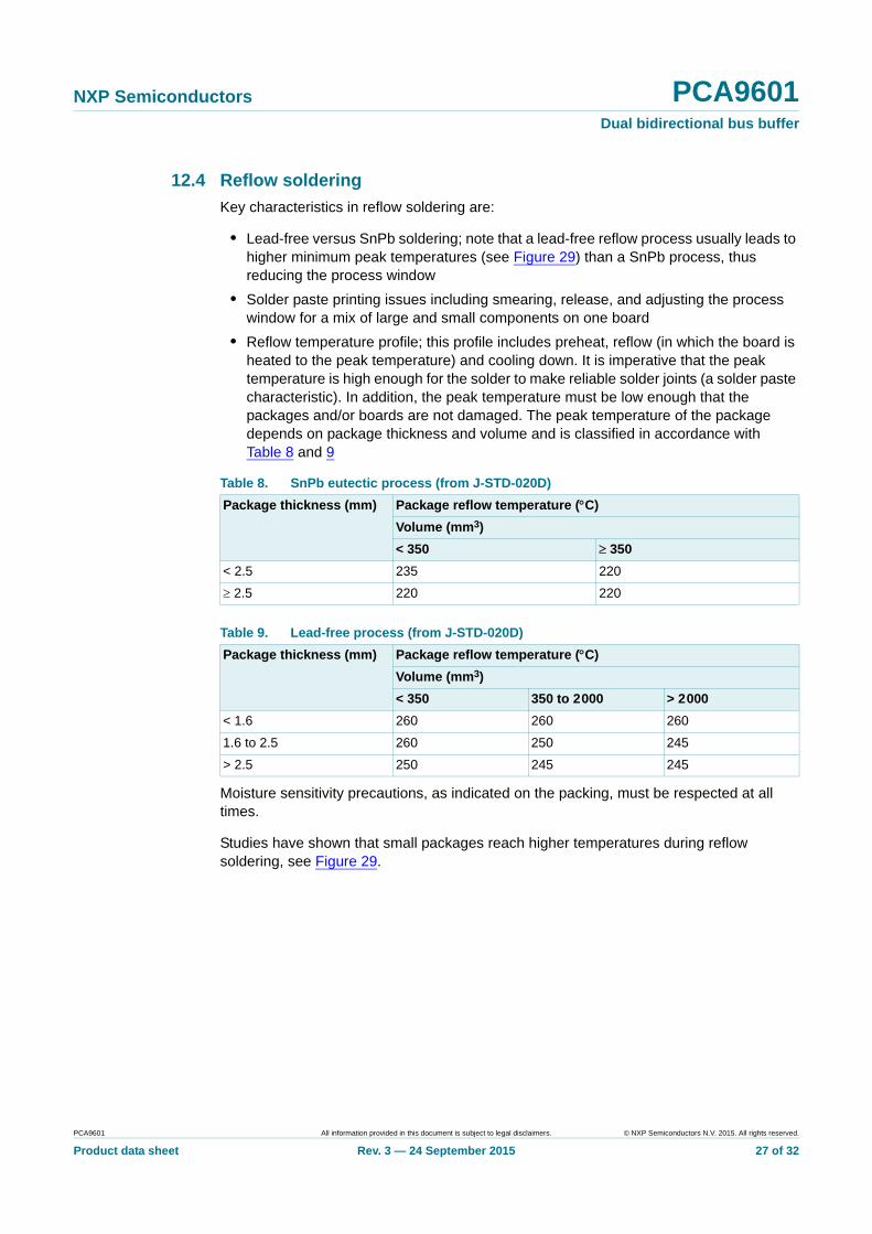
12.4 Reflow soldering
Key characteristics in reflow soldering are:
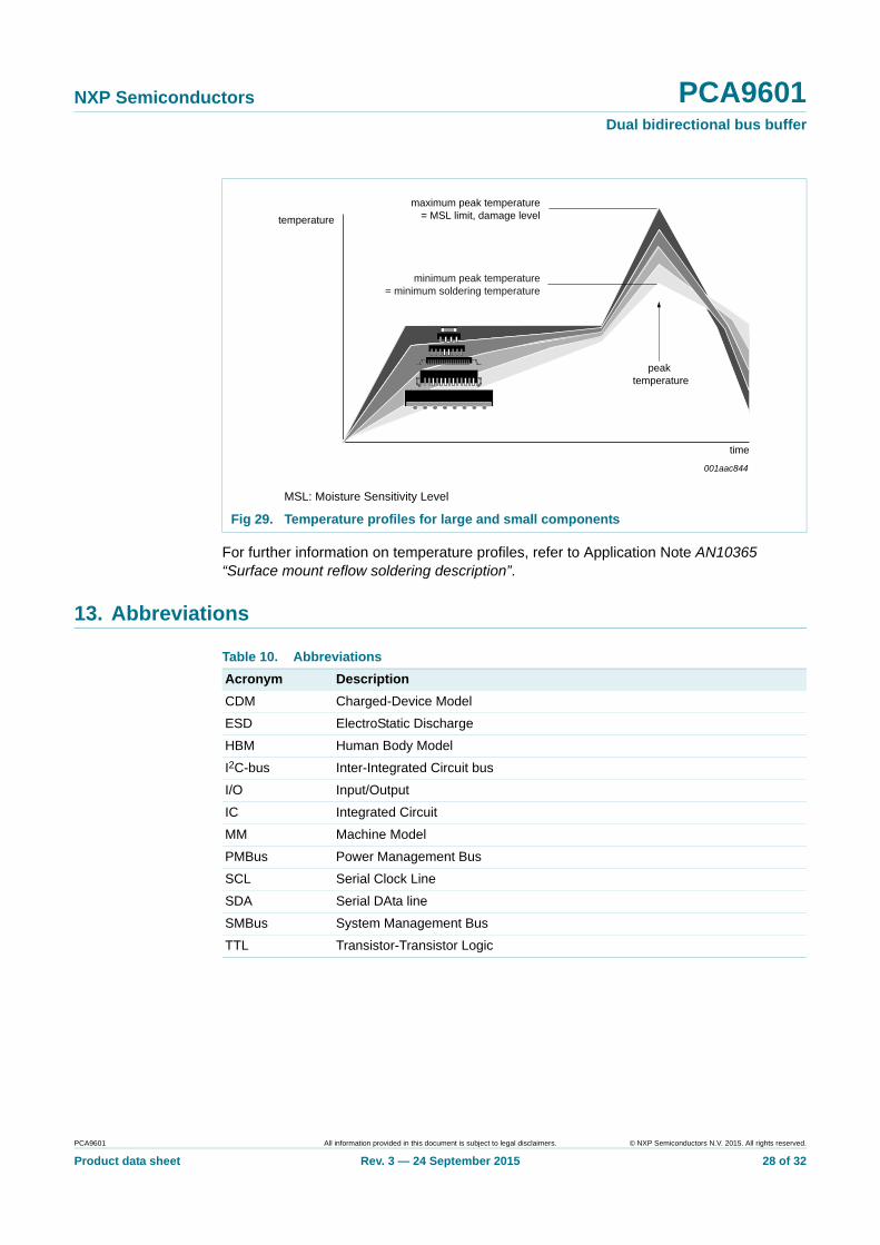
• Lead-free versus SnPb soldering; note that a lead-free reflow process usually leads to higher minimum peak temperatures (see Figure 29) than a SnPb process, thus reducing the process window
• Solder paste printing issues including smearing, release, and adjusting the process window for a mix of large and small components on one board
• Reflow temperature profile; this profile includes preheat, reflow (in which the board is heated to the peak temperature) and cooling down. It is imperative that the peak temperature is high enough for the solder to make reliable solder joints (a solder paste characteristic). In addition, the peak temperature must be low enough that the packages and/or boards are not damaged. The peak temperature of the package depends on package thickness and volume and is classified in accordance with Table 8 and 9
Moisture sensitivity precautions, as indicated on the packing, must be respected at all times.
Studies have shown that small packages reach higher temperatures during reflow soldering, see Figure 29.
Table 8. SnPb eutectic process (from J-STD-020D)
Package thickness (mm) Package reflow temperature (C)
Volume (mm3)
< 350 350
< 2.5 235 220
2.5 220 220
Table 9. Lead-free process (from J-STD-020D)
Package thickness (mm) Package reflow temperature (C)
Volume (mm3)
< 350 350 to 2000 > 2000
< 1.6 260 260 260
1.6 to 2.5 260 250 245
> 2.5 250 245 245
PCA9601 All information provided in this document is subject to legal disclaimers. © NXP Semiconductors N.V. 2015. All rights reserved.
Product data sheet Rev. 3 — 24 September 2015 27 of 32
NXP Semiconductors PCA9601Dual bidirectional bus buffer
For further information on temperature profiles, refer to Application Note AN10365 “Surface mount reflow soldering description”.
13. Abbreviations
MSL: Moisture Sensitivity Level
Fig 29. Temperature profiles for large and small components
001aac844
temperature
time
minimum peak temperature= minimum soldering temperature
maximum peak temperature= MSL limit, damage level
peak temperature
Table 10. Abbreviations
Acronym Description
CDM Charged-Device Model
ESD ElectroStatic Discharge
HBM Human Body Model
I2C-bus Inter-Integrated Circuit bus
I/O Input/Output
IC Integrated Circuit
MM Machine Model
PMBus Power Management Bus
SCL Serial Clock Line
SDA Serial DAta line
SMBus System Management Bus
TTL Transistor-Transistor Logic
PCA9601 All information provided in this document is subject to legal disclaimers. © NXP Semiconductors N.V. 2015. All rights reserved.
Product data sheet Rev. 3 — 24 September 2015 28 of 32
NXP Semiconductors PCA9601Dual bidirectional bus buffer
14. Revision history
Table 11. Revision history
Document ID Release date Data sheet status Change notice Supersedes
PCA9601 v.3 20150924 Product data sheet - PCA9601 v.2
Modifications: • HBM corrected from “4500 V” to “3500 V”. Original material was retested and is 3.5 kV
• Updated Section 4 “Ordering information”
• Table 4 “PCA9601/PCA9600 versus P82B96”: Deleted reference to DIP8 in P82B96 package column
PCA9601 v.2 20110506 Product data sheet - PCA9601 v.1
PCA9601 v.1 20100528 Product data sheet - -
PCA9601 All information provided in this document is subject to legal disclaimers. © NXP Semiconductors N.V. 2015. All rights reserved.
Product data sheet Rev. 3 — 24 September 2015 29 of 32
NXP Semiconductors PCA9601Dual bidirectional bus buffer
15. Legal information
15.1 Data sheet status
[1] Please consult the most recently issued document before initiating or completing a design.
[2] The term ‘short data sheet’ is explained in section “Definitions”.
[3] The product status of device(s) described in this document may have changed since this document was published and may differ in case of multiple devices. The latest product status information is available on the Internet at URL http://www.nxp.com.
15.2 Definitions
Draft — The document is a draft version only. The content is still under internal review and subject to formal approval, which may result in modifications or additions. NXP Semiconductors does not give any representations or warranties as to the accuracy or completeness of information included herein and shall have no liability for the consequences of use of such information.
Short data sheet — A short data sheet is an extract from a full data sheet with the same product type number(s) and title. A short data sheet is intended for quick reference only and should not be relied upon to contain detailed and full information. For detailed and full information see the relevant full data sheet, which is available on request via the local NXP Semiconductors sales office. In case of any inconsistency or conflict with the short data sheet, the full data sheet shall prevail.
Product specification — The information and data provided in a Product data sheet shall define the specification of the product as agreed between NXP Semiconductors and its customer, unless NXP Semiconductors and customer have explicitly agreed otherwise in writing. In no event however, shall an agreement be valid in which the NXP Semiconductors product is deemed to offer functions and qualities beyond those described in the Product data sheet.
15.3 Disclaimers
Limited warranty and liability — Information in this document is believed to be accurate and reliable. However, NXP Semiconductors does not give any representations or warranties, expressed or implied, as to the accuracy or completeness of such information and shall have no liability for the consequences of use of such information. NXP Semiconductors takes no responsibility for the content in this document if provided by an information source outside of NXP Semiconductors.
In no event shall NXP Semiconductors be liable for any indirect, incidental, punitive, special or consequential damages (including - without limitation - lost profits, lost savings, business interruption, costs related to the removal or replacement of any products or rework charges) whether or not such damages are based on tort (including negligence), warranty, breach of contract or any other legal theory.
Notwithstanding any damages that customer might incur for any reason whatsoever, NXP Semiconductors’ aggregate and cumulative liability towards customer for the products described herein shall be limited in accordance with the Terms and conditions of commercial sale of NXP Semiconductors.
Right to make changes — NXP Semiconductors reserves the right to make changes to information published in this document, including without limitation specifications and product descriptions, at any time and without notice. This document supersedes and replaces all information supplied prior to the publication hereof.
Suitability for use — NXP Semiconductors products are not designed, authorized or warranted to be suitable for use in life support, life-critical or safety-critical systems or equipment, nor in applications where failure or malfunction of an NXP Semiconductors product can reasonably be expected to result in personal injury, death or severe property or environmental damage. NXP Semiconductors and its suppliers accept no liability for inclusion and/or use of NXP Semiconductors products in such equipment or applications and therefore such inclusion and/or use is at the customer’s own risk.
Applications — Applications that are described herein for any of these products are for illustrative purposes only. NXP Semiconductors makes no representation or warranty that such applications will be suitable for the specified use without further testing or modification.
Customers are responsible for the design and operation of their applications and products using NXP Semiconductors products, and NXP Semiconductors accepts no liability for any assistance with applications or customer product design. It is customer’s sole responsibility to determine whether the NXP Semiconductors product is suitable and fit for the customer’s applications and products planned, as well as for the planned application and use of customer’s third party customer(s). Customers should provide appropriate design and operating safeguards to minimize the risks associated with their applications and products.
NXP Semiconductors does not accept any liability related to any default, damage, costs or problem which is based on any weakness or default in the customer’s applications or products, or the application or use by customer’s third party customer(s). Customer is responsible for doing all necessary testing for the customer’s applications and products using NXP Semiconductors products in order to avoid a default of the applications and the products or of the application or use by customer’s third party customer(s). NXP does not accept any liability in this respect.
Limiting values — Stress above one or more limiting values (as defined in the Absolute Maximum Ratings System of IEC 60134) will cause permanent damage to the device. Limiting values are stress ratings only and (proper) operation of the device at these or any other conditions above those given in the Recommended operating conditions section (if present) or the Characteristics sections of this document is not warranted. Constant or repeated exposure to limiting values will permanently and irreversibly affect the quality and reliability of the device.
Terms and conditions of commercial sale — NXP Semiconductors products are sold subject to the general terms and conditions of commercial sale, as published at http://www.nxp.com/profile/terms, unless otherwise agreed in a valid written individual agreement. In case an individual agreement is concluded only the terms and conditions of the respective agreement shall apply. NXP Semiconductors hereby expressly objects to applying the customer’s general terms and conditions with regard to the purchase of NXP Semiconductors products by customer.
No offer to sell or license — Nothing in this document may be interpreted or construed as an offer to sell products that is open for acceptance or the grant, conveyance or implication of any license under any copyrights, patents or other industrial or intellectual property rights.
Document status[1][2] Product status[3] Definition
Objective [short] data sheet Development This document contains data from the objective specification for product development.
Preliminary [short] data sheet Qualification This document contains data from the preliminary specification.
Product [short] data sheet Production This document contains the product specification.
PCA9601 All information provided in this document is subject to legal disclaimers. © NXP Semiconductors N.V. 2015. All rights reserved.
Product data sheet Rev. 3 — 24 September 2015 30 of 32
NXP Semiconductors PCA9601Dual bidirectional bus buffer
Export control — This document as well as the item(s) described herein may be subject to export control regulations. Export might require a prior authorization from competent authorities.
Non-automotive qualified products — Unless this data sheet expressly states that this specific NXP Semiconductors product is automotive qualified, the product is not suitable for automotive use. It is neither qualified nor tested in accordance with automotive testing or application requirements. NXP Semiconductors accepts no liability for inclusion and/or use of non-automotive qualified products in automotive equipment or applications.
In the event that customer uses the product for design-in and use in automotive applications to automotive specifications and standards, customer (a) shall use the product without NXP Semiconductors’ warranty of the product for such automotive applications, use and specifications, and (b) whenever customer uses the product for automotive applications beyond NXP Semiconductors’ specifications such use shall be solely at customer’s
own risk, and (c) customer fully indemnifies NXP Semiconductors for any liability, damages or failed product claims resulting from customer design and use of the product for automotive applications beyond NXP Semiconductors’ standard warranty and NXP Semiconductors’ product specifications.
Translations — A non-English (translated) version of a document is for reference only. The English version shall prevail in case of any discrepancy between the translated and English versions.
15.4 TrademarksNotice: All referenced brands, product names, service names and trademarks are the property of their respective owners.
I2C-bus — logo is a trademark of NXP Semiconductors N.V.
16. Contact information
For more information, please visit: http://www.nxp.com
For sales office addresses, please send an email to: [email protected]
PCA9601 All information provided in this document is subject to legal disclaimers. © NXP Semiconductors N.V. 2015. All rights reserved.
Product data sheet Rev. 3 — 24 September 2015 31 of 32
NXP Semiconductors PCA9601Dual bidirectional bus buffer
17. Contents
1 General description . . . . . . . . . . . . . . . . . . . . . . 1
2 Features and benefits . . . . . . . . . . . . . . . . . . . . 1
3 Applications . . . . . . . . . . . . . . . . . . . . . . . . . . . . 2
4 Ordering information. . . . . . . . . . . . . . . . . . . . . 24.1 Ordering options . . . . . . . . . . . . . . . . . . . . . . . . 2
5 Block diagram . . . . . . . . . . . . . . . . . . . . . . . . . . 3
6 Pinning information. . . . . . . . . . . . . . . . . . . . . . 36.1 Pinning . . . . . . . . . . . . . . . . . . . . . . . . . . . . . . . 36.2 Pin description . . . . . . . . . . . . . . . . . . . . . . . . . 3
7 Functional description . . . . . . . . . . . . . . . . . . . 47.1 Static level offset card side . . . . . . . . . . . . . . . . 47.1.1 Fast-mode operation . . . . . . . . . . . . . . . . . . . . 47.1.2 Fast-mode Plus operation . . . . . . . . . . . . . . . . 47.2 High drive, long distance side. . . . . . . . . . . . . . 57.3 Connections to other bus buffers . . . . . . . . . . . 57.4 Comparison of PCA9601/PCA9600
and P82B96 . . . . . . . . . . . . . . . . . . . . . . . . . . . 6
8 Limiting values. . . . . . . . . . . . . . . . . . . . . . . . . . 7
9 Characteristics. . . . . . . . . . . . . . . . . . . . . . . . . . 8
10 Application information. . . . . . . . . . . . . . . . . . 1310.1 Calculating system delays and bus clock
frequency . . . . . . . . . . . . . . . . . . . . . . . . . . . . 1510.2 Negative undershoot below absolute minimum
value . . . . . . . . . . . . . . . . . . . . . . . . . . . . . . . . 1910.2.1 Example with questions and answers. . . . . . . 21
11 Package outline . . . . . . . . . . . . . . . . . . . . . . . . 24
12 Soldering of SMD packages . . . . . . . . . . . . . . 2612.1 Introduction to soldering . . . . . . . . . . . . . . . . . 2612.2 Wave and reflow soldering . . . . . . . . . . . . . . . 2612.3 Wave soldering . . . . . . . . . . . . . . . . . . . . . . . . 2612.4 Reflow soldering . . . . . . . . . . . . . . . . . . . . . . . 27
13 Abbreviations. . . . . . . . . . . . . . . . . . . . . . . . . . 28
14 Revision history. . . . . . . . . . . . . . . . . . . . . . . . 29
15 Legal information. . . . . . . . . . . . . . . . . . . . . . . 3015.1 Data sheet status . . . . . . . . . . . . . . . . . . . . . . 3015.2 Definitions. . . . . . . . . . . . . . . . . . . . . . . . . . . . 3015.3 Disclaimers . . . . . . . . . . . . . . . . . . . . . . . . . . . 3015.4 Trademarks. . . . . . . . . . . . . . . . . . . . . . . . . . . 31
16 Contact information. . . . . . . . . . . . . . . . . . . . . 31
17 Contents . . . . . . . . . . . . . . . . . . . . . . . . . . . . . . 32
© NXP Semiconductors N.V. 2015. All rights reserved.
For more information, please visit: http://www.nxp.comFor sales office addresses, please send an email to: [email protected]
Date of release: 24 September 2015
Document identifier: PCA9601
Please be aware that important notices concerning this document and the product(s)described herein, have been included in section ‘Legal information’.
Related Documents