ATA6570 High-speed CAN Transceiver with Partial Networking DATASHEET COMPLETE Features • High speed CAN transceiver fully compliant to ISO 11898-2, ISO11898-5, ISO11898-6, ISO/DIS 11898-2 (2016) and SAEJ2962-2 • Autonomous bus biasing according to ISO 11898-6 • Low electromagnetic emission (EME) and high electromagnetic immunity (EMI) • Standard CAN data rate up to 1Mbit/s and CAN FD data rate up to 5Mbit/s (CAN FD) • 4Mbit/s SPI interface • Differential bus receiver with wide common mode range • Very low current consumption in Sleep and Standby with fully wake-up capability • Power-down of the complete node via the INH-output (switching off external voltage regulator(s)) • Six operation modes – Power off mode – Microcontroller Reset mode – Sleep mode – Standby mode – Normal mode – Overtemp mode • Four wake-up sources – Local wake-up via pin WAKE – Remote wake-up pattern according to ISO 11898-5 – Remote wake-up frame according to ISO 11898-6 (selective wake-up) – Host wake-up via SPI • Wake-up source recognition • Transceiver disengages from the bus in over-temperature and low power supply mode • RXD recessive clamping detection • Transmit data (TXD) dominant timeout function • Undervoltage detection on VS, VCC and VIO pins Atmel-9340D-ATA6570_Datasheet_Complete-11/2016

Welcome message from author
This document is posted to help you gain knowledge. Please leave a comment to let me know what you think about it! Share it to your friends and learn new things together.
Transcript

ATA6570
High-speed CAN Transceiver with PartialNetworking
DATASHEET COMPLETE
Features
bull High speed CAN transceiver fully compliant to ISO 11898-2ISO11898-5 ISO11898-6 ISODIS 11898-2 (2016) and SAEJ2962-2
bull Autonomous bus biasing according to ISO 11898-6bull Low electromagnetic emission (EME) and high electromagnetic
immunity (EMI)bull Standard CAN data rate up to 1Mbits and CAN FD data rate up to
5Mbits (CAN FD)bull 4Mbits SPI interfacebull Differential bus receiver with wide common mode rangebull Very low current consumption in Sleep and Standby with fully wake-up
capabilitybull Power-down of the complete node via the INH-output (switching off
external voltage regulator(s))bull Six operation modes
ndash Power off modendash Microcontroller Reset modendash Sleep modendash Standby modendash Normal modendash Overtemp mode
bull Four wake-up sourcesndash Local wake-up via pin WAKEndash Remote wake-up pattern according to ISO 11898-5ndash Remote wake-up frame according to ISO 11898-6 (selective
wake-up)ndash Host wake-up via SPI
bull Wake-up source recognitionbull Transceiver disengages from the bus in over-temperature and low
power supply modebull RXD recessive clamping detectionbull Transmit data (TXD) dominant timeout functionbull Undervoltage detection on VS VCC and VIO pins
Atmel-9340D-ATA6570_Datasheet_Complete-112016
bull Overtemperature protectionbull 33V to 5V microcontrollers can be interfaced directly via the VIO pinbull Battery supply and CAN bus pins protected against transients according to ISO7637bull High Electro Static Discharge (ESD) Handling Capability on the Bus Pinsbull Bus pins short-circuit protected to GND and VCCbull VS operating voltage up to 28V VS DC supply voltage up to 42Vbull Watchdog with independent clock sourcebull Watchdog can be operated in Window and Timeout mode
ndash Optional cyclic wake-up in watchdog Timeout modendash Watchdog automatically re-enabled when wake-up event capturedndash Watchdog period selectablendash Watchdog reset period selectable
bull Qualified according to AEC-Q100bull Fulfills the OEM Hardware Requirements for CAN Interfaces in Automotive Applications Rev 13bull Fulfills the OEM Requirements for Partial Networking Rev 22bull SO14 Package
Description
The Atmelreg ATA6570 is a standalone high speed CAN transceiver that interfaces a Controller AreaNetwork (CAN) protocol controller and the physical two wire CAN bus designed for high speed CANapplications in the automotive environment
It provides local and enhanced remote wake-up capabilities and is available in a SO14 package TheAtmel ATA6570 has a very low power consumption in Standby and Sleep Mode Beside local wake-up viaWAKE and remote wake-up pattern according to ISO 11898-5 ATA6570 additionally supportsISO11898-6 compliant CAN partial networking A CAN frame decoder evaluates the bus traffic andchecks for a matching frame that has being configured into registers via the SPI The device is able tokeep the complete ECU in a low power mode even when bus traffic is present until a valid wake-up frameis received It also features a watchdog and a Serial Peripheral Interface (SPI)
The Atmel ATA6570 is a CAN-FD device and can be easily configured via the SPI as Non-FD (meaningonly for Classical CAN) CAN FD silent CAN FD passive or as CAN FD active device in order to fulfill thecorresponding application requirements
The VIO pin allows the automatic adjustment of the IO levels to the IO level of the connectedmicrocontroller
The SPI interface controls the device and provides status and diagnosis information to the Host MCU
All these features make the Atmel ATA6570 an excellent choice for high speed CAN networks especiallyin applications where nodes are always connected with the battery but are only activated when they arereally needed in the application
Atmel High-speed CAN Transceiver with Partial Networking [DATASHEET]Atmel-9340D-ATA6570_Datasheet_Complete-112016
2
Figure -1 Simplified Block Diagram
Filter and Compare
Wake-upConfiguration
Decoding
TXD
VCC
RXD
VIO
WAKE
MISO
MOSI
SCK
NCS
CANL
CANH
1
3
13
12
2
10
7
4
5
9
6
11
8
14
VS
INH
GND
Receiver
Mod
e C
ontr
ol
Bus
Bias
ing
Error Handling
CAN FD
Partial Networking
Watchdog
InternalOscillator
Transceiver
Atmel High-speed CAN Transceiver with Partial Networking [DATASHEET]Atmel-9340D-ATA6570_Datasheet_Complete-112016
3
Table of Contents
Features 1
Description2
1 Pin Configuration 511 Supply Pin (VS) 512 Ground Pin (GND)513 Supply Pin (VCC) 614 Supply Pin (VIO)615 Bus Pins (CANH AND CANL)616 Input Pin (TXD)617 Output Pin (RXD)618 Inhibit Output Pin (INH) 719 Wake Input Pin (WAKE only ATA6570) 7110 SPI Input Pin (MOSI)7111 SPI Output Pin (MISO) 7112 SPI Clock Pin (SCK)7113 SPI Chip Select Pin (NCS) 8
2 Functional Description 921 Device Operation Modes922 Integrated CAN Transceiver Operation Modes 1323 Wake-up in ATA65701924 Fail-safe Features3325 WUP Detection and Bias Control 3726 Device ID3827 Lock Control Register3828 Window Watchdog3829 General-purpose Memory (GPMn)43210 VIO Supply Pin 44211 VCCVIO Undervoltage Protection 44212 Serial Peripheral Interface (SPI)45
3 Absolute Maximum Ratings50
4 Thermal Characteristics51
5 Electrical Characteristics 52
6 Application Circuits 58
7 Ordering Information59
8 Package Information60
9 Revision History61
Atmel High-speed CAN Transceiver with Partial Networking [DATASHEET]Atmel-9340D-ATA6570_Datasheet_Complete-112016
4
1 Pin ConfigurationFigure 1-1 Pin Configuration
1
2
3
4 SO14
5
6
7
TXD
GND
VCC
RXD
VIO
MISO
INH
NCS
CANH
CANL
MOSI
VS
WAKE
SCK
14
13
12
11
10
9
8
Table 1-1 Pin Description
Pin Symbol Function
1 TXD Transmit data input
2 GND Ground
3 VCC 5V CAN transceiver supply voltage
4 RXD Receive data output reads out data from the CAN-bus
5 VIO Supply voltage for IO level adaptor
6 MISO MISO SPI data output
7 INH High-side output for switching external voltage regulators
8 SCK SPI clock
9 WAKE High voltage input for local wake-up
10 VS Battery supply voltage
11 MOSI MOSI SPI data input
12 CANL Low level CAN bus line
13 CANH High level CAN bus line
14 NCS NCS SPI chip select input
11 Supply Pin (VS)The VS supply pin is the power supply pin for the Atmelreg ATA6570 device In an application this pinusually is connected to the battery via a serial diode for reverse battery protection This pin sustainsstandard automotive conditions such as 40V during load dump
An undervoltage detection circuit is implemented to avoid a malfunction or false bus messages Afterswitching on VS the IC starts in Standby mode and the INH output is switched on
12 Ground Pin (GND)The IC does not affect the CAN bus in the event of GND disconnection
Atmel High-speed CAN Transceiver with Partial Networking [DATASHEET]Atmel-9340D-ATA6570_Datasheet_Complete-112016
5
13 Supply Pin (VCC)This is the supply pin for the CANH and CANL bus drivers the bus differential receiver and the busbiasing voltage circuitry VCC is monitored for under voltage conditions
14 Supply Pin (VIO)This is the supply pin for the digital inputoutputs pins VIO is monitored for undervoltage conditions SeeFail-safe Mechanisms
15 Bus Pins (CANH AND CANL)These are the CAN bus terminals
CANL is a low side driver to GND and CANH is a high side driver to VCC In Normal mode and TXDhigh the CANH and CANL drivers are off and the voltage at CANH and CANL is approximately 25Vprovided by the internal bus biasing circuitry This state is called recessive
When TXD is low CANL is pulled to GND and CANH to VCC creating a differential voltage on the CANbus This state is called dominant state
In Standby mode the CANH and CANL drivers are off If the device is in unpowered mode or sleepmode CANH and CANL are highly resistive with extremely low leakage current to GND making thedevice ideally passive
Pins CANH and CANL have integrated ESD protection and extremely high robustness versus externaldisturbance such as EMC and electrical transients The CANH and CANL bus outputs are short-circuitprotected either against GND or a positive supply voltage and are also protected against over-temperature conditions
16 Input Pin (TXD)This is the device input pin to control the CAN bus level In the application this pin is connected to themicrocontroller transmit terminal Pin TXD has an internal pull-up towards VIO to ensure a safe definedrecessive driver state in case this pin is left floating
In Normal mode when TXD is high or floating the CAN bus is driven to the recessive state
TXD must be pulled to GND in order to activate the CANH and CANL drivers and set the bus to thedominant state A TXD dominant timeout timer is started when the TXD pin is set to low If the low stateon the TXD pin persists for longer than tto(dom) TXD the transmitter is disabled releasing the bus lines torecessive state This function prevents a hardware andor software application failure from driving the buslines to a permanent dominant state (blocking all network communications) The TXD dominant timeouttimer is reset when the TXD pin is set to high
The transmitter is also disabled if pin TXD is held low (eg by a short- circuit to GND) during the deviceis switched into Normal mode the bus lines are in the recessive state The transceiver remains in thisstate until pin TXD goes high
17 Output Pin (RXD)In Normal and Silent mode this pin reports the state of the CAN bus to the microcontroller In theapplication this pin is connected to the microcontroller receive terminal RXD is high when the bus isrecessive When the bus is dominant RXD is low
Atmel High-speed CAN Transceiver with Partial Networking [DATASHEET]Atmel-9340D-ATA6570_Datasheet_Complete-112016
6
The output is a push-pull structure the high side is connected to VIO and the low-side to GND
In Standby mode the RXD output is switched to VIO When a wake-up event is detected RXD will beforced to low
A RXD recessive clamping function (see section RXD Recessive Clamping) is implemented This fail-safefeature prevents the controller from sending data on the bus if the RXD line is clamped to high (egrecessive)
18 Inhibit Output Pin (INH)The inhibit output pin provides an internal switch towards VS and is used to control external voltageregulators If the device is in normal or standby mode the inhibit high-side switch is turned on When thedevice is in sleep mode the inhibit switch is turned off thus disabling the connected external voltageregulators or other connected external devices
A wake-up event on the CAN bus or at the WAKE pin switches the INH pin to the VS level After a systempower-up (VS rises from zero) the INH pin switches to the VS level automatically
The INH output pin has an additional function when the watchdog is enabled At every watchdog reset theINH pin will be switched off for a pre-defined time This will trigger a power-on reset of the microcontrollerif the supply of the microcontroller is controlled by the INH pin
19 Wake Input Pin (WAKE only ATA6570)In the Atmelreg ATA6570 this pin is a high-voltage input used for waking up the device from sleep mode Itis usually connected to an external switch in the application to generate a local wake-up If the WAKE pinis not needed in the application the local wake-up should be disabled and the WAKE pin should beconnected to GND to ensure optimal EMI performance
The WAKE pin has a special design structure and is triggered by a LOW-to-HIGH andor a HIGH-to-LOWtransition on the WAKE pin This arrangement allows for maximum flexibility when designing a localwake-up circuit
An internal filter is implemented to avoid a false wake-up event due to parasitic pulses A serial resistorshould be inserted in order to limit the input current mainly during transient pulses and ESD Therecommended resistor value is 10kΩ An external 10nF capacitor is advised for better EMC and ESDperformances
110 SPI Input Pin (MOSI)Master-Out-Slave-In serial data port input connected to an output of the microcontroller
111 SPI Output Pin (MISO)Master-In-Slave-Out serial data port output connected to an input of the microcontroller this pin is in tri-state if NCS is high
112 SPI Clock Pin (SCK)Serial data clock default level is low due to internal pull-down
Atmel High-speed CAN Transceiver with Partial Networking [DATASHEET]Atmel-9340D-ATA6570_Datasheet_Complete-112016
7
113 SPI Chip Select Pin (NCS)Chip select pin active low If chip select is not active no data are loaded from MOSI on SCK edges orprovided at MISO
Atmel High-speed CAN Transceiver with Partial Networking [DATASHEET]Atmel-9340D-ATA6570_Datasheet_Complete-112016
8
2 Functional Description
21 Device Operation Modes
Figure 2-1 Overview to the Device Operation Modes
Power Off
a VVS = VVS_PWRONb VVS lt VVS_PWROFF
i VVCC lt VVCC_UV_Set for at least tUV2Sleepj VVIO lt VVIO_UV_Set for at least tUV2Sleep
l reset finishedm watchdog activated ampamp any reset event
c DOPM = Normald overtemperature detectede wake-up event system eventf DOPM = Standbyg DOPM = Sleeph no wake-up event pending
k number of enabled wake-up source ge 1
a
m
m
b
l
f or (g and (h or k)
(g and h and k) or i or j
(g and h and k) or i or j
e or f
MicrocontrollerReset
Standby SleepOvertemp
c
d
d
c
Normal
The mode control unit in the Atmelreg ATA6570 implements 6 different states as depicted in Figure 2-1 Allof the states are briefly described in this section
211 Power Off ModeThe device is in Power off mode when the supply voltage of the device VVS is lower than the defineddevice power off detection voltage threshold (VVS_PWROFF) This is the default mode when the battery isfirst connected In this mode the integrated CAN transceiver is in the TRX off mode (see section TRX OffMode) The watchdog is also in off mode The pins CANH CANL are high ohmic and the INH output isswitched off The device is not able to provide any functionality As soon as VVS rises above the power ondetection threshold (VVS_PWRON) the device boots up The whole device is reset and initialized Aftertstartup the device is in the Standby mode
212 Standby ModeThe Standby mode is the default mode after a power on reset In Standby mode the integrated CANtransceiver is unable to transmit or receive data The INH pin is at the VS level and the external voltageregulator controlled by the pin is switched on
The Atmelreg ATA6570 supports the autonomous bus biasing according to ISO 11898-6 in Standby- andSleep Mode (provided VVS gt VVS_UV_CAN_Clear) The bus pins are biased to GND (via RCANH RCANL) whenthe bus is inactive and at approximately 25V when there is a remote CAN bus wake-up request (Wake-Up Pattern WUP according to ISO 11898-6) detected
In Standby mode the Atmel ATA6570 supports both CAN bus remote wake-up via a standard wake-uppattern (WUP) and via a selective wake-up frame (WUF) The CAN bus remote wake-up is only activatedwhen the register bit CWUE is set to lsquo1rsquo (see section TRXECR ndash Transceiver Event Capture Enable
Atmel High-speed CAN Transceiver with Partial Networking [DATASHEET]Atmel-9340D-ATA6570_Datasheet_Complete-112016
9
Register (address 0x23)) The low power wake-up comparator in the receiver then monitors thecorresponding bus activities and wakes up the whole device after detecting a valid wake-up event (VVSmust above the VS CAN undervoltage release threshold Otherwise the integrated transceiver is in TRXoff mode and no Bus wake-up can be detected)
In the case that CPNE = PNCFOK = lsquo1rsquo the selective wake-up is enabled After a successful detection ofa wake-up pattern the bus pin is first biased to 25V and the device is ready for decoding further comingwake-up frames (WUF) Only after detecting a valid WUF a wake up event is registered and the wake upprocess is finished Decoding of CAN data and remote frames is supported during all mode transitions ofthe device If the data frame is a valid WUF the device will indicate a wake-up event
If the selective wake-up is disabled and CAN remote wake-up is enabled the standard wake-up via wake-up pattern (WUP) is activated The device biases its bus pin to 25V after a successful detection of awake up pattern registers the wake-up event and the wake-up process is finished
The device also supports detecting system events (see section Wake-up and Interrupt Event Diagnosisvia Pin RXD ) and a local wake-up event via the WAKE pin in Standby mode The internal wake-up flagsCWUS LWURS and LWUFS (see sections TRXESR ndash Transceiver Event Status Register (address 0x63)and WKESR ndash WAKE Event Status Register (address 0x64)) and system event status registers are set tolsquo1rsquo by the device if the corresponding event is detected
The device will not leave the Standby mode after detecting a valid wake-up event It will only set thecorresponding internal status register bits A transition to the Normal mode will only happen when theregister bits DOPM are set to lsquo111rsquo via SPI
In Standby mode the detection of a wake-up event or an interrupt event (see section Wake-up andInterrupt Event Diagnosis via Pin RXD ) is denoted via pin RXD provided that the corresponding eventinterrupt is enabled (see section SECR ndash System Event Capture Enable Register (address 0x04) tosection WKECR ndash WAKE Event Capture Enable Register (address 0x4C)) The RXD pin is usually at VVIOlevel and will be forced to low if an enabled event is detected At the same time a set of status registers(see section GESR ndash Global Event Status Register (address 0x60) to section WKESR ndash WAKE EventStatus Register (address 0x64)) is provided which allows the microcontroller to get further detailedinformation about the device via SPI
As shown in Figure 2-1 the device will enter the Standby mode in following cases
1 from Power off mode after power on reset after VVS rises above the power on detection voltagethreshold VVS_PWRON or
2 from Overtemp mode after the chip temperature falls below the over-temperature release thresholdTOT_Release or
3 from Sleep mode after detecting enabled wake-up event or interrupt event or4 from Sleep mode Normal mode via SPI (DOPM=0x4) if a valid interface voltage VVIO is applied or5 if try switching to sleep mode (DOPM=0x1 is written) via SPI when there is a wake-up event
pending or all wake-up sources are disabled
The watchdog can be activated (Window or Timeout mode) in Standby mode and it can only beconfigured in Standby mode in order to avoid unwanted configuration of the watchdog
213 Sleep ModeThe Sleep mode is the most power saving mode of the device In this mode the INH output is switchedoff Therefore the external voltage regulator(s) controlled by this pin is also switched-off This is the onlydifference between Sleep mode and Standby mode If a valid interface supply voltage (VVIO) is appliedregisters of the device can still be accessed via its SPI interface
Atmel High-speed CAN Transceiver with Partial Networking [DATASHEET]Atmel-9340D-ATA6570_Datasheet_Complete-112016
10
As in Standby mode the device can react on a variety of wake-up events (see section Wake-up inATA6570) Customers are allowed to configure the device to let it be woken up in different ways If a validinterface voltage VVIO is applied it is even possible to wake-up the device from Sleep mode via a SPIcommand (DOPM = StandbyNormal)
In Sleep mode the INH output switches on when either a CAN bus wake-up event or a host wake-upevent (via SPI) or a local wake-up or an interrupt event (see section Interrupt EventWake-up EventDelay ) is detected or a watchdog reset (Timeout mode is enabled) occurs and the device switches tomicrocontroller reset mode
As shown in Figure 2-1 the device enters the Sleep mode in following cases
1 From the Normal mode or Standby mode via an SPI command if no wake-up event is pending andat least one wake-up source (see section Wake-up in ATA6570) is enabled or
2 From the Normal mode or Standby mode in the case of detecting VCC or VIO undervoltage (VVIO ltVVIO_UV_Set or VVCC lt VVCC_UV_Set for t gt tUV2Sleep) In this case all pending wake-up events will becleared CAN bus wake-up (CWUE = 1 see section TRXECR ndash Transceiver Event Capture EnableRegister (address 0x23)) and local wake-up via the WAKE pin (LWUFE = 1 ampamp LWURE = 1) areenabled Selective wake-up is disabled (please refer to section VCCVIO Undervoltage Protectionfor details about VCCVIO undervoltage protection)
The Atmelreg ATA6570 provides a bit SMTS (see DMSR ndash Device Mode Status Register (address 0x03)) todenote whether the recent transition to the Sleep mode is triggered by a VCCVIO undervoltage event ornot The bit can be read by the microcontroller in the Sleep mode (if a valid interface supply voltage isprovided) or after waking up from the Sleep mode
214 Normal ModeThe Atmelreg ATA6570 provides its full functionality in the Normal mode
Wake-up flag CWUS and interrupt event status registers will still be set to lsquo1rsquo by the device if thecorresponding event is detected
As shown in Figure 2-1 the device will enter the Normal mode from the Standby mode or Sleep mode viaan SPI command
215 Overtemp ModeThe Overtemp mode is the operation mode which protects the device from an over-temperature damageThe over-temperature protection is only active in Normal mode
The device provides two levels of over-temperature protection In the case that the chip temperature risesabove the over-temperature protection prewarning threshold (T gt TOT_Prew) the device first set the statusbit OTPWS = 1 If the over-temperature prewarning interrupt is enabled (OTPWE = 1) an over-temperature prewarning interrupt will be generated (OTPW = 1 RXD signalization if COPM = 00 andDOPM = 111 (Normal mode))
The device will enter the Overtemp mode when the chip temperature rises above the over-temperatureprotection shutdown threshold (TOT_Sdwn) In the Overtemp mode the integrated CAN transceiver isswitched to the TRX Off mode The CAN bus pins are high ohmic No further wake-up event will bedetected but the pending wake-upinterrupt event will still be signaled by a low level on pin RXDAs shown in Figure 2-1 the device will enter the Overtemp mode from Normal mode when the chiptemperature rises up the over-temperature protection shutdown threshold
The device will exit the Overtemp mode and enter the Standby mode when the chip temperature fallsbelow the over-temperature protection release threshold (TOT_Release) or when the device is powered off
Atmel High-speed CAN Transceiver with Partial Networking [DATASHEET]Atmel-9340D-ATA6570_Datasheet_Complete-112016
11
216 Microcontroller Reset ModeReset mode only exists when the watchdog is activated In this mode the INH output is switched off andthe transceiver is disabled The device leaves the Reset mode when the reset pulse width is reached
Table 2-1 Operating Modes and Functions
Block Device Operating Mode
Power off Standby Normal Sleep Overtemp
SPI disabled active active active if VIOsupplied disabled
INH high-ohmic VS level VS level high-ohmic VS level
CAN TRX OffTRX Standby
TRX BiasedStandby
TRX Normal TRX Standby
TRX BiasedStandby TRX
Silent (determinedby bits COPM)
TRX Standby TRX Biased
StandbyTRX Off
RXD VIO level
VIO level low ifwake-up
interrupt eventdetected
CAN bit stream ifCOPM = 011011 otherwise sameas StandbySleep
VIO level low ifwake-up interrupt
event detected
VIO level low ifwake-up
interrupt eventpending
217 Related Registers
2171 DMCR ndash Device Mode Control Register (address 0x01)The device operation mode is selected via bits DOPM in the device mode control register The register isaccessed via SPI at address 0x01
Bit 7 6 5 4 3 2 1 0
- - - - - DOPM[20] DMCR
ReadWrite R R R R R RW RW RW
Initial Value 0 0 0 0 0 1 0 0
Bit 73 Reserved for future use
Bit 20 DOPM[20] ndash Select device operation mode
DOPM[20] Device Operation Mode
3rsquob001 Sleep mode
3rsquob100 Standby mode
3rsquob111 Normal mode
2172 DMSR ndash Device Mode Status Register (address 0x03)The register provides device operation mode transition related information to the external microcontroller
Atmel High-speed CAN Transceiver with Partial Networking [DATASHEET]Atmel-9340D-ATA6570_Datasheet_Complete-112016
12
Bit 7 6 5 4 3 2 1 0
SMTS OTPWS NMTS - DMSR
ReadWrite R R R R R R R R
Initial Value 0 0 1 0 0 0 0 0
Bit 7 SMTS Sleep mode transition status
The device sets the bit to lsquo0rsquo if the recent transition to Sleep mode is triggered by an SPI command andsets the bit to lsquo1rsquo if the recent transition to Sleep mode is forced by an VCCVIO undervoltage
Bit 6 OTPWS over-temperature prewarning status
The device sets the bit to lsquo1rsquo if IC temperature is over over-temperature prewarning threshold and to lsquo0rsquovice versa
Bit 5 NMTS Normal mode transition status
The device sets the bit to lsquo0rsquo when IC has entered Normal mode after power-up and set the bit to lsquo1rsquo whenthe IC has powered up but has not yet switched to Normal mode
Bit 40 Reserved for future use
22 Integrated CAN Transceiver Operation ModesThe integrated high-speed CAN transceiver in the Atmelreg ATA6570 is designed for standard bit rates upto 1Mbits and CAN Flexible Data Rate (CAN-FD) bit rates up to 5Mbits It provides differential transmitand receive capability to a CAN protocol controller The transceiver is ISO 11898-2 ISO 11898-5 ISO11898-6 and ISODIS 11898-2 (2016) compliant
The integrated CAN transceiver supports four operating modes TRX Normal TRX Silent TRX Standbyand TRX Biased Standby (see Figure 2-2) The CAN transceiver operation mode depends on the deviceoperation mode and on the setting of bits COPM in the CAN mode control register (see section TRXCR ndashCAN Transceiver Control Register (address 0x20)) When the device is in normal mode all four operationmodes can be selected The TRX biased standby mode can not be selected via the COPM bits directlyRefer to sectionTRX Biased Standby Mode The operating modes of the integrated transceiver can beselected via bits COPM in the CAN mode control register (see section TRXCR ndash CAN Transceiver ControlRegister (address 0x20)) When the device is in Standby or Sleep mode the transceiver is either in TRXStandby mode or in TRX Biased Standby mode
The CAN transceiver supports autonomous bus biasing according to ISO 11898-6 It is active in CANTRX Standby mode The bus is biased to 25V if there is activity on the bus (TRX Biased Standby mode)In TRX Biased Standby mode the CAN bias voltage is derived directly from VVS If there is no activity onthe bus for t gt tSilence the bus is biased to GND (TRX Standby mode)
In other transceiver active operation modes namely TRX Normal or TRX Silent mode the bus pinsCANH and CANL are biased to 25V (see section TRXCR ndash CAN Transceiver Control Register (address0x20)) The CAN bias voltage is derived from VVCC in TRX Normal mode and derived from VVS in TRXSilent mode In TRX off mode the bus pins are highly resistive and the transceiver is disengaged fromthe bus
Atmel High-speed CAN Transceiver with Partial Networking [DATASHEET]Atmel-9340D-ATA6570_Datasheet_Complete-112016
13
Figure 2-2 Overview to the Integrated CAN TRX Operation Modes
TRX OffModeTX offRX off
RXD VIO levelCANHL tri-state
a Device in (Power Off or Overtemp or Reset mode) or VVS lt VVS_UV_CAN_Setb VVS gt VVS_UV_CAN_Clear and device not in Power Off and Overtemp mode
i DOPM = Normalj TXD = HIGH
l COPM = TRX Normal mode with 2rsquob01m COPM = TRX Normal mode with 2rsquob10n RXD recessive clamping detectedo VVCC has been smaller than VVCC_TX_Sd for tSUP_UV_filterp VVCC has been larger than or equal to VVCC_TX_Sd for tSUP_UV_filter
c Bus wake-up event or DOPM = Normal and COPM = TRX Normal with 2lsquob01 and VVCC has been smaller than VVCC_TX_Sd for tSUP_UV_filterd for t gt tsilence no bus activity detectede t lt tsilencef VVCC gt VVCC_UV_Set for tSUP_UV_filterg COPM = TRX Silent and DOPM = Normalh (DOPM = Sleep or Standby) or (DOPM = Normal and COPM = TRX Standby)
k VVCC lt VVCC_UV_Set for tSUP_UV_filter
b
a
all modes
a
i and [ (p and l) or m] and n and j
g or n
g or n
g or (i and [ (p and l)or m] and j)
d and (h or (k and I))
d and (h or (k and I))
i and [ (p and I) or m] and j
d and (h or k and I)
d and (h or k and I)
i and l and o
i and l and p
i and [ (p and I) or m] and j
(i and I and o) or(g and n)
g
d and h
e and h
TRX StandbyModeTX offRX off
RXD wake-upHighCANHL Ground
cd
TRX BiasedModeTX offRX off
RXD wake-upHighCANHL 25V (VS)
TRX SilentModeTX offRX on
RXD bit streamCANHL 25V (VS)
TRX NormalModeTX onRX on
RXD bit streamCANHL 25V (VCC)
TRX ReducedNormal Mode
TX offRX on
RXD bit streamCANHL 25V (VS)
221 TRX Off ModeThe CAN transceiver is completely switched off in the TRX Off mode The CAN bus pins CANH CANLare highly resistive and RXD pin is at the VIO level
As shown in Figure 2-2 the integrated CAN transceiver will enter the TRX Off mode in following cases
1 the device switches to Power off mode or2 the device switches to Overtemp mode or3 VVS falls below the CAN undervoltage detection threshold VVS_UV_CAN_Set
It will be switched on again and enter CAN TRX Standby mode when VVS rises above the CANundervoltage release threshold and the device is no longer in Power Off Overtemp mode
Atmel High-speed CAN Transceiver with Partial Networking [DATASHEET]Atmel-9340D-ATA6570_Datasheet_Complete-112016
14
222 TRX Standby ModeIn the TRX Standby mode the transmitter and the receiver are switched off to reduce currentconsumption The wake-up comparator monitors the bus lines for a valid remote bus wake-up pattern(WUP) provided CAN bus wake-up detection is enabled (CWUE=1) Two periods of dominant bus-levelsseparated by a period of recessive bus-level each of at least tFilter switches the RXD pin to low to signal awake-up request to the microcontroller Figure 2-3 describes the process and timing of the WUPdetection In the TRX Standby mode the bus lines are biased to ground to reduce current consumption toa minimum
Figure 2-3 Timing of CAN Standard Wake-Up via Wake-Up Pattern (WUP)
tdom = tFilter tdom = tFiltertrec = tFilter
t le tWake
VDiff
dominantCANH
CANL
RXD
recessive
Bus-wake-upis signalled
dominant
As shown in Figure 2-2 the CAN transceiver will enter the TRX Standby mode in following cases
1 when the device leaves Power off mode or Overtemp mode and sufficient VVS is applied or2 any of the conditions for CAN TRX Biased Standby mode are valid for longer than tSilence (see
section TRX Biased Standby Mode)
223 TRX Biased Standby ModeThe CAN transceiver behavior in the TRX Biased Standby mode is basically the same as in the TRXStandby mode The only difference is that in the TRX Biased Standby mode the bus pins are biased to25V The integrated CAN transceiver will enter this mode when activity is detected on the CAN bus whilethe transceiver is in TRX Standby mode The transceiver will return to TRX Standby mode if the CAN busis silent for longer than tSilence (see section WUP Detection and Bias Control)
As shown in Figure 2-2 the CAN transceiver will enter the TRX Biased Standby mode in following cases
1 From TRX SilentNormalReduced normal mode when tSilence time out is not detected and thedevice is in Standby (DOPM = 100) or Sleep mode (DOPM = 001) or
2 From TRX SilentNormalReduced normal mode when tSilence time out is not detected and thedevice is in Normal mode (DOPM = 111) and the COPM is set to TRX Standby mode (COPM = 00)or
3 From TRX NormalReduced normal mode (COPM = 01) when VCC lt VVCC_UV_Set is detected andtSilence time out is not detected or
4 From TRX Standby mode when the device is in Normal mode (DOPM = 111) COPM is set to TRXNormal mode (COPM = 01) and VCC lt VVCC_TX_Sd has been detected or
5 From TRX Standby mode when a wake-up event is detected on the CAN bus
Atmel High-speed CAN Transceiver with Partial Networking [DATASHEET]Atmel-9340D-ATA6570_Datasheet_Complete-112016
15
224 TRX Silent ModeThe TRX Silent mode is a receive-only mode of the CAN transceiver It can be used for instance to testthe connection of the bus medium or for the software-driven selective wake-up In the TRX Silent modethe device can still receive data from the bus but the transmitter is disabled and therefore no data can besent to the CAN bus The bus pins are released to recessive state All other IC functions continue tooperate as they do in the TRX Normal mode CAN biasing remains active Silent mode can be used toprevent a faulty CAN controller from disrupting all network communicationsAs shown in Figure 2-2 the CAN transceiver will enter the TRX Silent mode in following cases
1 the device is in Normal mode (DOPM = Normal) and CAN transceiver is in TRX Silent mode(COPM = TRX Silent)
2 the device is in Normal mode and CAN transceiver is in TRX Normal mode and a RXD recessiveclamping failure is detected
It will remain in TRX Silent mode if VCC undervoltage is detected or a RXD recessive clamping failure isdetected even if CAN TRX Normal mode is selected in device Normal mode
225 TRX Normal ModeIn the TRX Normal mode the integrated transceiver is able to transmit and receive data via the CANH andCANL bus lines The output driver stage is active and drives data from the TXD input to the CAN bus Thereceiver converts the analog data on the bus lines into digital data which is output to pin RXD The busbiasing is set to VVCC2 and the undervoltage monitoring of VVCC is active
The slope of the output signals on the bus lines is controlled and optimized in a way that guarantees thelowest possible electromagnetic emission (EME)
As shown in Figure 2-2 the CAN transceiver will enter the TRX Normal mode in following cases
1 the device is in Normal mode (DOPM = Normal) AND the CAN transceiver has been enabled bysetting bits COPM to lsquo01rsquo or lsquo10rsquo AND no VCC undervoltage is detected AND no RXD recessiveclamping is detected
2 the transceiver is in the TRX Reduced Normal mode and VVCC gt VVCC_TX_Sd for t gt tSUP_UV_filter
If pin TXD is held low (eg by a short-circuit to GND) when CAN TRX Normal mode is selected via bitsCOPM the transceiver will not enter CAN TRX Normal mode but will switch to or remain in TRX Silentmode It will remain in TRX Silent mode until pin TXD goes high in order to prevent a hardware andorsoftware application failure from driving the bus lines to an unwanted dominant state
The application can determine whether the CAN transceiver is ready to transmit data or is disabled byreading the CAN Transmitter Status bit (TXS) bit in the Transceiver Status Register (see section TRXSRndash CAN Transceiver Status Register (address 0x22))
226 TRX Reduced Normal ModeIn the TRX Reduced Normal mode the transmitter is switched off as VCC is lower than the VVCC_TX_Sdthreshold All other features available in the TRX Normal mode is also provided in the TRX ReducedNormal mode
As shown in Figure 2-2 the CAN transceiver will enter the TRX Reduced Normal mode when thetransceiver is in TRX Normal mode and VVCC lt VVCC_TX_Sd for t gt tSUP_UV_filter
Atmel High-speed CAN Transceiver with Partial Networking [DATASHEET]Atmel-9340D-ATA6570_Datasheet_Complete-112016
16
227 Related Registers
2271 TRXCR ndash CAN Transceiver Control Register (address 0x20)
Bit 7 6 5 4 3 2 1 0
- CFDPE PNCFOK CPNE - - COPM[10] TRXCR
Read Write R RW RW RW R R RW RW
Initial Value 0 1 0 0 0 0 0 1
Bit 7 Reserved for future use
Bit 6 CFDPE The external microcontroller should set the bit to lsquo1rsquo to enable the CAN FD passive featurewhen selective wake-up is activated should set the bit to lsquo0rsquo vice versa The bit is set to 1 by default afterpower on reset The bit shall be set to 1 for continuous sending dom-rec bits with a bitrate higher than1Mbits
Bit 5 PNCFOK The external microcontroller should set the bit to lsquo1rsquo after successfully configuring thepartial networking registers and to lsquo0rsquo vice versa In addition the device will reset the bit to 0automatically after any write access to the partial networking configuration related registers
Bit 4 CPNE The external microcontroller should set the bit to lsquo1rsquo to enable selective wake-up and to lsquo0rsquovice versa
Bit 32 Reserved for future use
Bit 10 COPM (The TRXCR register is a control register Therefore the state of the transceiver will notbe mirrored to this register COPM bit only defines the expected state of the transceiver when the deviceis switched to Normal mode The finite state machine in Figure 2-2 will not change the COPM bits) [10] ndashSelect CAN Transceiver operation mode
COPM[10] CAN TRX Operation Mode
2rsquob00 TRX Standby mode
2rsquob01
TRX Normal mode (when DOPM = Normal) VCC undervoltage detectionactive for the transceiver finite state machine The transceiver switches to theTRX biased Standby mode immediately after detecting the VCCundervoltage
2rsquob10
TRX Normal mode (when DOPM = Normal) VCC undervoltage detectioninactive for the transceiver finite state machine The transceiver switches fromTRX NormalReduced Normal mode to TRX biased Standby mode when thedevice is forced to Sleep mode by a VCC undervoltage event
2rsquob11 TRX Silent mode
Atmel High-speed CAN Transceiver with Partial Networking [DATASHEET]Atmel-9340D-ATA6570_Datasheet_Complete-112016
17
2272 TRXSR ndash CAN Transceiver Status Register (address 0x22)
Bit 7 6 5 4 3 2 1 0
TXS PNERRS PNCFS PNOSCS CBSS - VCCS TXDOUT TRXSR
ReadWrite R R R R R R R R
Initial Value 0 1 0 0 1 0 0 0
Bit 7 TXS Transmitter status the device sets the bit to lsquo1rsquo if the transmitter is ready to transmit data andto lsquo0rsquo if CAN transmitter is disabled
Bit 6 PNERRS Partial networking error detection status the device sets the bit to lsquo0rsquo if no CAN partialnetworking error detected (PNEFD = 0 ampamp PNCFOK = 1 ampamp no oscillator hardware failure detected(default)) to lsquo1rsquo vice versa (PNEFD = 1 || PNCFOK = 0)
Bit 5 PNCFS Partial networking configuration status the device sets the bit to lsquo0rsquo if partial networkingconfiguration error is detected (PNCFOK = 0) to lsquo1rsquo vice versa
Bit 4 PNOSCS Partial networking oscillator ok the device sets the bit to lsquo1rsquo if CAN partial networkingoscillator is running at target frequency to lsquo0rsquo vice versa
Bit 3 CBSS Bus status the device sets the bit to lsquo1rsquo if CAN bus is inactive (for longer than tSilence) to lsquo0rsquovice versa
Bit 2 Reserved for future use
Bit 1 VCCS VVCC status the device sets the bit to lsquo1rsquo if VVCC is below the undervoltage detectionthreshold to lsquo0rsquo vice versa
Bit 0 TXDOUT TXD time out status the device sets the bit to lsquo1rsquo if CAN transmitter is disabled due to aTXD dominant timeout event to lsquo0rsquo if no TXD dominant timeout event was detected
2273 BFIR - Bus Failure Indication Register (address 0x33)
Bit 7 6 5 4 3 2 1 0
- - - - - - BOUT BSC BFIR
Read Write R R R R R R R R
Initial Value 0 0 0 0 0 0 0 0
Bit 72 Reserved for future use
Bit 1 BOUT bus dominant timeout event indicator the BOUT bit shows the current status of the busdominant timeout detection If the bit reads lsquo1rsquo the bus is currently in dominant timeout state otherwisethe bit reads lsquo0rsquo
Bit 0 BSC bus short-circuit event capture indicator the BSC bit shows the current status of the busshort-circuit event detection If the bit reads lsquo1rsquo the bus is currently in short-circuit state otherwise the bitreads lsquo0rsquo
Atmel High-speed CAN Transceiver with Partial Networking [DATASHEET]Atmel-9340D-ATA6570_Datasheet_Complete-112016
18
2274 TRXESR2 ndash Transceiver Event Status Register 2 (address 0x35)
Bit 7 6 5 4 3 2 1 0
- - - - - - - RXDRCS TRXESR2
Read Write R R R R R R R R
Initial Value 0 0 0 0 0 0 0 0
Bit 71 Reserved for future use
Bit 0 RXDRCS RXD recessive clamping status the device sets the bit to lsquo1rsquo if the event is enabled in theTRXECR2 register and a RXD recessive clamping event is detected The bit is reset to lsquo0rsquo by the deviceeither when the device enters sleep or standby or unpowered mode or the RXD pin shows dominantagain
23 Wake-up in ATA6570
231 Local Wake-up via Pin WAKEThe device provides the high voltage WAKE input pin that can be used to wake up the device It is anedge sensitive pin (low to-high or high to low transition) Thus even if the WAKE pin is at high or lowvoltage it is possible to switch the IC into the Sleep mode It is usually connected to the ignition forgenerating a local wake-up in the application if the ignition is switched on
A glitch suppression circuit is integrated to avoid unexpected wake-up on the Wake pin The voltage onthe pin is detected as stable only when the level remains stable for tlocal_wu Therefore a local wake-uprequest is detected when the logic level on the pin WAKE has been already stable for at least tlocal_wu andthe new level remains stable for at least tlocal_wu
Local wake-up via pin WAKE can be enableddisabled via the register bits LWUFE and LWURE (seesection WKECR ndash WAKE Event Capture Enable Register (address 0x4C)) and the logic level at pinWAKE can be read via the register PWKS (see section PWKS ndash Pin WAKE Status Register (address0x4B)) if a valid interface voltage VVIO is provided
To reduce the battery current during low-power mode the Wake pin has internal pull-uppull-down currentsthat are activated when a stable level at the wake pin has been detected
bull High level on pin is followed by an internal pull up towards VSbull Low level is followed by an internal pull down towards GND
Local wake-up can only be activated in Standby and Sleep mode In Normal mode the status of thevoltage on pin WAKE can always be read via bit PWKVS Otherwise PWKVS is only valid if local wake-up is enabled In applications that donrsquot make use of the local wake-up facility local wake-up should be disabled and theWAKE pin should be connected to GND to ensure optimal EMI performance
232 Remote Wake-up Pattern according to ISO 11898-5 (Partial Networking Disabled)If the CAN transceiver is in TRX Standby mode and CAN bus wake-up is enabled (CWUE = 1) but CANselective wake-up is disabled (CPNE = 0 or PNCFOK = 0) the device will monitor the bus for a standardwake-up pattern as specified in ISO11898-5
This filtering helps to avoid spurious wake-up events which could be triggered by for example adominant clamped bus or by dominant phases due to noise spikes on the bus transients or EMI
Atmel High-speed CAN Transceiver with Partial Networking [DATASHEET]Atmel-9340D-ATA6570_Datasheet_Complete-112016
19
The wake-up pattern consists of multiple consecutive dominant bus levels for a duration of at least tFiltereach separated by a recessive bus level with a duration of at least tFilter Dominant or recessive bits in-between the above mentioned phases which are shorter than tFilter are ignored
The complete dominant-recessive-dominant pattern as shown in Figure 2-3 must be received withintWake to be recognized as a valid wake-up pattern Otherwise the internal wake-up logic is reset Thecomplete wake-up pattern will then need to be retransmitted to trigger a wake-up event
When a valid CAN WUP is detected on the bus the wake-up bit CWUS in the transceiver event statusregister is set (see section TRXESR ndash Transceiver Event Status Register (address 0x63)) and pin RXD isdriven low If the device was in Sleep mode when the wake-up event was detected it will switch pin INHto VS to activate external voltage regulators (eg for supplying VCC and VIO) and enter Standby mode
CAN wake-up via WUP can only be disabled via bit CWUE If CWUE is set to lsquo0rsquo no remote wake-up viathe CAN bus is possible In case CWUE is set to lsquo1rsquo and selective wake-up is disabled the device willswitch to Standby mode after detecting the wake-up pattern (WUP) coming from Sleep mode In caseCWUE is set to lsquo1rsquo and the selective wake-up is enabled the device will first switch on the bus biasingafter detecting the WUP and will only switch afterwards to the Standby mode when it detects a validWUF (please refer to the next section for WUF)
233 Remote Wake-up Frame according to ISO 11898-6
2331 CAN Selective Wake-upPartial networking makes it possible for a CAN node or a CAN sub-network to be woken up individually bymeans of dedicated and predefined frames the so called wake-up frames (WUF) When a particularnodersquos tasks are not required it is in selective sleep mode
The transceiver monitors the bus for dedicated CAN wake-up frames when both CAN wake-up (CWUE =lsquo1rsquo) and CAN selective wake-up (CPNE = lsquo1rsquo) are enabled and the partial networking registers areconfigured correctly (PNCFOK = lsquo1rsquo) An accurate oscillator and a low power high speed comparator arerunning in this case to support the correct detection of the wake-up frame
According to ISO11898-1 a wake-up frame is a CAN frame consisting of an identifier field (ID) a DataLength Code (DLC) a data field and a Cyclic Redundancy Check (CRC) code including the CRCdelimiter
The wake-up CAN frame (ID and data) is fully configurable via SPI communication A standard (11-bit) orextended (29-bit) identifier for the wake-up frame format can be selected via bit IDE in the Frame controlregister CFCR (see section CFCR - CAN Frame Configuration Register (address 0x2F))
In the ID registers (see section CIDR0 - CAN ID Register 0 (address 0x27) to section CIDR3 - CAN IDRegister 3 (address 0x2A)) a valid WUP can be defined and stored To allow a group of identifiers to berecognized as valid by an individual node an ID mask (see section CIDMR0 - CAN ID Mask Register 0(address 0x2B) to section CIDMR3 - CAN ID Mask Register 3 (address 0x2E)) can be defined in themask registers where a 1 means lsquodont carersquo
A single wake-up frame can wake up multiple groups of nodes by comparing the incoming data field withthe data mask as the data field indicates which nodes are to be woken up Groups of nodes can be pre-defined and associated with bits in a data mask
The number of data bytes expected in the data field of a CAN wake-up frame are set with the data lengthcode (bits DLC in the frame control register in section CFCR - CAN Frame Configuration Register(address 0x2F)) If DLC ne 0000 (one or more data bytes expected) at least one bit in the data field of thereceived wake-up frame must be set to 1 and at least one equivalent bit in the associated data maskregister in the transceiver (register for data mask to be defined) must also be set to 1 for a successful
Atmel High-speed CAN Transceiver with Partial Networking [DATASHEET]Atmel-9340D-ATA6570_Datasheet_Complete-112016
20
wake-up Each matching pair of logic 1s indicates a group of nodes to be activated (since the data field isup to 8 bytes long up to 64 groups of nodes can be defined)
If DLC = 0000 a node will wake up if the WUF contains a valid identifier and the received data lengthcode is 0000 regardless of the values stored in the data mask If DLC ne 0000 and all data mask bits areset to 0 the device cannot be woken up via the CAN bus (note that all data mask bits are 1 per default) Ifa WUF contains a valid ID but the DLCs (in the Frame control register and in the WUF) donrsquot match thedata field is ignored and no nodes will be woken up The data length code and the data field can beexcluded from the evaluation of the wake-up frame If bit PNDM = 0 (see section CFCR - CAN FrameConfiguration Register (address 0x2F)) only the identifier field is evaluated to determine if the framecontains a valid wake-up frame If PNDM = 1 (the default value) the data field is included as part of thewake-up filtering
When PNDM = 0 a valid wake-up frame is detected and a wake-up event is captured (and CWUS is setto 1) when
bull the identifier field in the received wake-up frame matches the pattern in the ID registers afterfiltering AND
bull the CRC field in the received frame (including a recessive CRC delimiter) was received withouterror
When PNDM = 1 a valid wake-up frame is detected whenbull the identifier field in the received wake-up frame matches the pattern in the ID registers after
filtering ANDbull the frame is not a Remote frame ANDbull the data length code in the received frame matches the configured data length code (bits DLC)
ANDbull if the data length code is greater than 0 at least one bit in the data field of the received frame is set
and the corresponding bit in the associated data mask register is also set ANDbull the CRC field in the received frame (including a recessive CRC delimiter) was received without
error
The internal error counter will be incremented when an erroneous CAN frame (eg a lsquostuffingrsquo error) isreceived prior the ACK field If a CAN frame is received without any errors appearing in front of the ACKfield the counter will be decremented Any data received after the CRC delimiter and before the nextSOF will be ignored by the partial networking module If the counter overflows (FEC gt ERRCNT seesection EFCR - Error Frame Counter Threshold Register (address 0x3A)) a frame detect error iscaptured (PNEFD = 1 see section TRXESR ndash Transceiver Event Status Register (address 0x63)) and thedevice wakes up the counter is reset to zero when the bias is switched off and partial networking is re-enabled
If partial networking is assumed to be configured correctly the PNCFOK has to be set to 1 by theapplication software The PNCFOK will be cleared after a write access to any of the CAN partialnetworking configuration registers (see section DRCR - Data Rate Configuration Register (address 0x26)to CDMR07 - CAN Data Mask Registers 07 (address 0x68hellip0x6F))
Any valid wake-up pattern (according to ISO 11898-5-6) will trigger a wake- up event if selective wake-up is disabled (CPNE = 0) or partial networking is not configured correctly (PNCFOK = 0) and the CANtransceiver is in TXD Standby mode with wake-up enabled (CWUE = 1)
All wake-up patterns will be ignored if the CAN transceiver is in TRX NormalSilent mode or CAN wake-up is disabled (CWUE = 0)
Atmel High-speed CAN Transceiver with Partial Networking [DATASHEET]Atmel-9340D-ATA6570_Datasheet_Complete-112016
21
2332 CAN Selective Wake-up and CAN FDCAN Flexible Data-rate (CAN FD) is an improved CAN protocol in regards of bandwidth and payload Asspecified in ISO 11898-1 CAN FD is based on the CAN protocol and still uses the CAN bus arbitrationmethod However after the arbitration phase of a classical CAN frame the data rate is increased and thedata bits are transferred with a higher bit rate than in the arbitration phase and returns to the longer bittime at the CRC Delimiter before the receivers transmit their acknowledge bits Besides the increased bitspeed the new CAN FD allows date frames up to 64 bytes compared with the maximum of 8 bytes withclassical CAN
The Atmelreg ATA6570 can be configured to recognize CAN FD frames as valid frames When CFDPE = 1the error counter is decremented every time the control field of a CAN FD frame is received The deviceremains in Sleep mode (CAN FD-passive) with partial networking enabled CAN FD frames are neverrecognized as valid wake-up frames even if PNDM = 0 and the frame contains a valid ID After receivingthe control field of a CAN FD frame the device ignores further bus signals until idle is again detected
When CFDPE is set to 0 CAN FD frames are interpreted as frames with errors by the partial networkingmodule So the error counter is incremented when a CAN FD frame is received Bit PNEFD is set to 1and the device wakes up if the ratio of CAN FD frames to valid CAN frames exceeds the threshold thattriggers error counter overflow
In the presence of CAN FD frames the transceivers can behave as followsbull Non-FD (Only Classical CAN frames) Systematically disturbs CAN- FD frames (eg through
error frames) or wakes up or terminates reception (eg Bus Off) when all or some frames presenton the bus are CAN-FD frames
bull CAN FD silent Capable of receiving defined configurable Classical CAN frames while underdefined conditions successfully ignoring all CAN-FD frames when interleaved with Classical CANframes
bull CAN FD passive Capable of transmitting and receiving all Classical CAN frames while underdefined conditions successfully ignoring all FD frames when interleaved with Classical CAN frames
bull CAN FD active Capable of successfully transmitting and receiving CAN FD frames and ClassicalCAN frames in an interleaved fashion
The Atmel ATA6570 device can be configured into all four modes in order to serve best the givenapplication
234 Wake-up via SPIIn case of an SPI command while the system is in a low power mode but with enabled SPI interface thedevice shall be woken up and enter the operation mode issued together with the SPI command A SPIcommand failure for instance invalid length of SPI command write access to read-only register and etcwill also trigger an interrupt event of the device (see Table 2-3)
235 Related Registers for Configuring the CAN Partial Networking
2351 DRCR - Data Rate Configuration Register (address 0x26)
Bit 7 6 5 4 3 2 1 0
- - - - - DR[20] DRCR
Read Write R R R R R RW RW RW
Initial Value 0 0 0 0 0 1 0 1
Bit 74 Reserved for future use
Atmel High-speed CAN Transceiver with Partial Networking [DATASHEET]Atmel-9340D-ATA6570_Datasheet_Complete-112016
22
Bit 20 DR[20] ndash Select CAN data rate
DR[20] CAN Data Rate (Kbits)
3rsquob000 50
3rsquob001 100
3rsquob010 125
3rsquob011 250
3rsquob100 Reserved (intended for future use currently selects 500Kbits)
3rsquob101 500
3rsquob110 Reserved (intended for future use currently selects 500Kbits)
3rsquob111 1000
2352 CIDR0 - CAN ID Register 0 (address 0x27)
Bit 7 6 5 4 3 2 1 0
ID0[70] CIDR0
ReadWrite RW RW RW RW RW RW RW RW
Initial Value 0 0 0 0 0 0 0 0
Bit 70 ID0 bits ID07 to ID00 of the extended frame format
2353 CIDR1 - CAN ID Register 1 (address 0x28)
Bit 7 6 5 4 3 2 1 0
ID1[70] CIDR1
ReadWrite RW RW RW RW RW RW RW RW
Initial Value 0 0 0 0 0 0 0 0
Bit 70 ID1 bits ID15 to ID08 of the extended frame format
2354 CIDR 2 - CAN ID Register 2 (address 0x29)
Bit 7 6 5 4 3 2 1 0
ID2[70] CIDR2
ReadWrite RW RW RW RW RW RW RW RW
Initial Value 0 0 0 0 0 0 0 0
Bit 72 ID2 bits ID23 to ID18 of the extended frame format bits ID05 to ID00 of the standard frameformat
Bit 10 ID2 bits ID17 to ID16 of the extended frame format
Atmel High-speed CAN Transceiver with Partial Networking [DATASHEET]Atmel-9340D-ATA6570_Datasheet_Complete-112016
23
2355 CIDR3 - CAN ID Register 3 (address 0x2A)
Bit 7 6 5 4 3 2 1 0
- - - ID3[40] CIDR3
Read Write R R R RW RW RW RW RW
Initial Value 0 0 0 0 0 0 0 0
Bit 75 Reserved for future use
Bit 40 ID3 bits ID28 to ID24 of the extended frame format bits ID10 to ID06 of the standard frameformat
2356 CIDMR0 - CAN ID Mask Register 0 (address 0x2B)
Bit 7 6 5 4 3 2 1 0
IDM0[70] CIDMR0
ReadWrite RW RW RW RW RW RW RW RW
Initial Value 0 0 0 0 0 0 0 0
Bit 70 IDM0 Mask bits ID07 to ID00 of the extended frame format 1 means lsquodont carersquo
2357 CIDMR1 - CAN ID Mask Register 1 (address 0x2C)
Bit 7 6 5 4 3 2 1 0
IDM1[70] CIDMR1
ReadWrite RW RW RW RW RW RW RW RW
Initial Value 0 0 0 0 0 0 0 0
Bit 70 IDM1 Mask bits ID15 to ID08 of the extended frame format 1 means lsquodont carersquo
2358 CIDMR2 - CAN ID Mask Register 2 (address 0x2D)
Bit 7 6 5 4 3 2 1 0
IDM2[70] CIDMR2
ReadWrite RW RW RW RW RW RW RW RW
Initial Value 0 0 0 0 0 0 0 0
Bit 72 IDM2 Mask bits ID23 to ID18 of the extended frame format bits ID05 to ID00 of the standardframe format
Bit 10 IDM2 Mask bits ID17 to ID16 of the extended frame format 1 means lsquodont carersquo
2359 CIDMR3 - CAN ID Mask Register 3 (address 0x2E)
Bit 7 6 5 4 3 2 1 0
- - - IDM3[40] CIDMR3
Read Write R R R RW RW RW RW RW
Initial Value 0 0 0 0 0 0 0 0
Bit 75 Reserved for future use
Atmel High-speed CAN Transceiver with Partial Networking [DATASHEET]Atmel-9340D-ATA6570_Datasheet_Complete-112016
24
Bit 40 IDM3 Mask bits ID28 to ID24 of the extended frame format bits ID10 to ID06 of the standardframe format 1 means lsquodont carersquo
23510 CFCR - CAN Frame Configuration Register (address 0x2F)
Bit 7 6 5 4 3 2 1 0
IDE PNDM - - DLC[30] CFCR
Read Write RW RW R R RW RW RW RW
Initial Value 0 1 0 0 0 0 0 0
Bit 7 IDE Identifier format the external microcontroller should set the bit to lsquo1rsquo if identifier is in extendedframe format (29-bit) set to lsquo0rsquo if identifier is in standard frame format (11-bit)
Bit 6 PNDM Partial networking data mask the external microcontroller should set the bit lsquo1rsquo if data lengthcode and data field are evaluated at wake-up set to lsquo0rsquo if data length code and data field are lsquodonrsquot carersquofor wake-up
Bit 54 Reserved for future use
Bit 30 DLC[30] Data length configuration select number of data bytes expected in a CAN frame
DLC[30] Number of Data Bytes
4rsquob0000 0
4rsquob0001 1
4rsquob0010 2
4rsquob0011 3
4rsquob0100 4
4rsquob0101 5
4rsquob0110 6
4rsquob0111 7
4rsquob1000 8
4rsquob1001 to 4rsquob1111 Tolerated 8 bytes expected DM0 (data mask 0) ignored
23511 EFCR - Error Frame Counter Threshold Register (address 0x3A)
Bit 7 6 5 4 3 2 1 0
- - - EERCNT EFCR
ReadWrite R R R RW RW RW RW RW
Initial Value 0 0 0 1 1 1 1 1
Bit 75 Reserved for future use
Bit 40 Set the error frame counter overflow threshold If the counter overflows (counter gt ERRCNT) aframe detect error is captured (PNEFD = 1) and the device wakes up
Atmel High-speed CAN Transceiver with Partial Networking [DATASHEET]Atmel-9340D-ATA6570_Datasheet_Complete-112016
25
23512 FECR ndash Failure Error Counter Register (address 0x3B)
Bit 7 6 5 4 3 2 1 0
- - - FEC FECR
ReadWrite R R R RW RW RW RW RW
Initial Value 0 0 0 0 0 0 0 0
Bit 75 Reserved for future use
Bit 40 If the device receives a CAN frame containing errors (eg a lsquostuffingrsquo error) that are received inadvance of the ACK field an internal error counter is incremented If a CAN frame is received without anyerrors appearing in front of the ACK field the counter is decremented Data received after the CRCdelimiter and before the next SOF is ignored by the partial networking module If the counter overflows(FEC gt ERRCNT see section FECR ndash Failure Error Counter Register (address 0x3B)) a frame detecterror is captured (PNEFD = 1 see section TRXESR ndash Transceiver Event Status Register (address 0x63))and the device wakes up the counter is reset to zero when the bias is switched off and partial networkingis re-enabled
23513 GLFT ndash Glitch Filter Threshold Register (address 0x67)
Bit 7 6 5 4 3 2 1 0
- - - - - GLF[20] GLFT
Read Write R R R R R RW RW RW
Initial Value 0 0 0 0 0 0 1 0
Bit 73 Reserved for future use
Bit 20 Set the glitch filter threshold from 5 to 55 of the arbitration bit rate
GLF[20] samples(le500Kbits) samples(1Mbits)
3rsquob000 1 [lt242lt517] 1 [lt483lt1035]]
3rsquob001 2 [lt483lt776] 2 [lt966lt1552]
3rsquob010 3 [lt725lt1035] 3 [lt1449lt207]]
3rsquob011 4 [lt966lt1294] 4 [lt1932lt2087]
3rsquob100 5 [lt1208lt1552] 5 [lt2415lt3105]
3rsquob101 6 [lt1449lt1811] 6 [lt2899lt3622]
3rsquob110 7 [lt1691lt207] 7 [lt3382lt4140]
3rsquob111 24 [lt5797lt6469] 13 [lt628lt7245]
Assumption clock tolerance plusmn3 transmitter plusmn05 tolerance OSR(le500Kbits) = 40 OSR(1Mbits) = 20
Atmel High-speed CAN Transceiver with Partial Networking [DATASHEET]Atmel-9340D-ATA6570_Datasheet_Complete-112016
26
23514 CDMR07 - CAN Data Mask Registers 07 (address 0x68hellip0x6F)
Bit 7 6 5 4 3 2 1 0
DM0hellip7[70] CDMR
ReadWrite RW RW RW RW RW RW RW RW
Initial Value 1 1 1 1 1 1 1 1
Bit 70 DM0hellip7[70] data mask 0hellip7 configuration
Table 2-2 Data Mask and the CAN Data Filed
CAN frame DLC Byte 0 Byte 1 Byte 2 Byte 3 Byte 4 Byte 5 Byte 6 Byte 7 CRC
Data mask DLC gt 8 DM0 DM1 DM2 DM3 DM4 DM5 DM6 DM7 CRC
CAN frame DLC Byte 0 Byte 1 Byte 2 Byte 3 Byte 4 Byte 5 Byte 6 Byte 7 CRC
Data mask DLC = 8 DM0 DM1 DM2 DM3 DM4 DM5 DM6 DM7 CRC
CAN frame DLC Byte 0 Byte 1 Byte 2 Byte 3 Byte 4 Byte 5 Byte 6 Byte 7 CRC
Data mask DLC = 7 DM1 DM2 DM3 DM4 DM5 DM6 DM7 CRC
CAN frame DLC Byte 0 Byte 1 Byte 2 Byte 3 Byte 4 Byte 5 Byte 6 CRC
Data mask DLC = 6 DM2 DM3 DM4 DM5 DM6 DM7 CRC
CAN frame DLC Byte 0 Byte 1 Byte 2 Byte 3 Byte 4 Byte 5 CRC
Data mask DLC = 5 DM3 DM4 DM5 DM6 DM7 CRC
CAN frame DLC Byte 0 Byte 1 Byte 2 Byte 3 Byte 4 CRC
Data mask DLC = 4 DM4 DM5 DM6 DM7 CRC
CAN frame DLC Byte 0 Byte 1 Byte 2 Byte 3 CRC
Data mask DLC = 3 DM5 DM6 DM7 CRC
CAN frame DLC Byte 0 Byte 1 Byte 2 CRC
Data mask DLC = 2 DM6 DM7 CRC
CAN frame DLC Byte 0 Byte 1 CRC
Data mask DLC = 1 DM7 CRC
CAN frame DLC Byte 0 CRC
DM x
Bit 7 Bit 6 Bit 5 Bit 4 Bit 3 Bit 2 Bit 1 Bit 0
Byte x
Bit 7 Bit 6 Bit 5 Bit 4 Bit 3 Bit 2 Bit 1 Bit 0
Atmel High-speed CAN Transceiver with Partial Networking [DATASHEET]Atmel-9340D-ATA6570_Datasheet_Complete-112016
27
23515 BFECR - Bus Failure Event Capture Enable Register (address 0x32)
Bit 7 6 5 4 3 2 1 0
- - - - - - BOUTE BSCE BFECR
Read Write R R R R R R RW RW
Initial Value 0 0 0 0 0 0 0 0
Bit 72 Reserved for future use
Bit 1 BOUTE bus dominant timeout event capture enable the BOUTE bit must be set to lsquo1rsquo to enablethe bus dominant timeout detection Setting the bit to `0` disables the bus dominant timeout detection
Bit 0 BSCE bus short-circuit event capture enable the BSCE bit must be set to lsquo1rsquo to enable the busshort-circuit event detection Setting the bit to `0` disables the bus short-circuit event detection
23516 PWKS ndash Pin WAKE Status Register (address 0x4B)
Bit 7 6 5 4 3 2 1 0
- - - - - - PWKVS - PWKS
Read Write R R R R R R R R
Initial Value 0 0 0 0 0 0 0 0
Bit 72 Reserved for future use
Bit 1 PWKVS Pin WAKE voltage status the device sets the bit to lsquo1rsquo if WAKE is high to lsquo0rsquo if WAKE islow PWKVS is always ldquo0rdquo in power-down mode if local wake-up is disabled
Bit 0 Reserved for future use
23517 GESR ndash Global Event Status Register (address 0x60)
Bit 7 6 5 4 3 2 1 0
OSCS - BFES - WKES TRXES - SYSES GESR
Read Write R R R R R R R R
Initial Value 0 0 0 0 0 0 0 1
Bit 7 System oscillator status the device sets the bit to lsquo1rsquo if a hardware failure of the system oscillator isdetected and sets the bit to lsquo0rsquo when the system oscillator is disabled for power saving purpose or thehardware failure disappeared after the oscillator is enabled (for instance in device Normal mode)
Bit 6 Reserved for future use
Bit 5 Bus failure event status the device sets the bit to lsquo1rsquo if there is bus failure event pending (any bit inthe BFESR register is lsquo1rsquo) The bit reads lsquo0rsquo if all status bits in the BFESR register are cleared
Bit 4 Reserved for future use
Bit 3 WKES WAKE event status the device sets the bit to lsquo1rsquo if there is a wake pin event pending (any bitin the WKESR register is lsquo1rsquo) The bit reads lsquo0rsquo if all status bits in the WKESR register are cleared
Atmel High-speed CAN Transceiver with Partial Networking [DATASHEET]Atmel-9340D-ATA6570_Datasheet_Complete-112016
28
Bit 2 TRXES Transceiver event status the device sets the bit to lsquo1rsquo if there is a transceiver event pending(any bit in the TRXESR register is lsquo1rsquo) The bit reads lsquo0rsquo if all status bits in the TRXESR register arecleared
Bit 1 Reserved for future use
Bit 0 SYSES System event status the device sets the bit to lsquo1rsquo if there is a system event pending (any bitin the SESR register is lsquo1rsquo) The bit reads lsquo0rsquo if all status bits in the SESR register are cleared
23518 SESR ndash System Event Status Register (address 0x61)
Bit 7 6 5 4 3 2 1 0
- - - PWRONS - OTPW SPIFS - ESR
Read Write R R R RW R RW RW R
Initial Value 0 0 0 1 0 0 0 0
Bit 75 Reserved for future use
Bit 4 PWRONS Power on status the device sets the bit to lsquo1rsquo if the device has left Power off mode afterpower-on The bit can be reset to lsquo0rsquo by writing a lsquo1rsquo to the bit PWRONS is also cleared when the deviceis forced to sleep mode due to an undervoltage event The information stored in PWRONS could be lostin this case Bit NMTS in the Device Mode Status Register (DMSR) which is set to 0 when the deviceswitches to normal mode after power-on compensates for this
Bit 3 Reserved for future use
Bit 2 OTPW Overtemperature prewarning status the device sets the bit to lsquo1rsquo if the event is enabled inthe SECR register and the chip temperature has exceeded the overtemperature prewarning thresholdThe bit can be reset to lsquo0rsquo by writing a lsquo1rsquo to the bit OTPW is also cleared when the device is forced tosleep mode due to an undervoltage event
Bit 1 SPIFS SPI failure status the device sets the bit to lsquo1rsquo if the event is enabled in the SECR registerand an SPI failure is detected The bit can be reset to lsquo0rsquo by writing a lsquo1rsquo to the bit SPIFS is also clearedwhen the device is forced to sleep mode due to an undervoltage event
Bit 0 Reserved for future use
23519 TRXESR ndash Transceiver Event Status Register (address 0x63)
Bit 7 6 5 4 3 2 1 0
- - PNEFD BS - - TRXF CWUS TRXESR
Read Write R RW RW RW R R RW RW
Initial Value 0 0 0 0 0 0 0 0
Bit 76 Reserved for future use
Bit 5 PNEFD Partial networking frame detection status the device sets the bit to lsquo1rsquo if a partialnetworking frame detection error is detected (error counter overflow) The bit can be reset to lsquo0rsquo by writinga lsquo1rsquo to the bit PNEFD is also cleared when the device is forced to sleep mode due to an undervoltageevent
Atmel High-speed CAN Transceiver with Partial Networking [DATASHEET]Atmel-9340D-ATA6570_Datasheet_Complete-112016
29
Bit 4 BS Bus status the device sets the bit to lsquo1rsquo if the event is enabled in the TRXECR register and noactivity on CAN bus is detected for tSilence The bit can be reset to lsquo0rsquo by writing a lsquo1rsquo to the bit BS is alsocleared when the device is forced to sleep mode due to an undervoltage event
Bit 32 Reserved for future use
Bit 1 TRXF Transceiver failure status the device sets the bit to lsquo1rsquo if the event is enabled in the TRXECRregister and a CAN failure event was detected The bit can be reset to lsquo0rsquo by writing a lsquo1rsquo to the bit TRXFis also cleared when the device is forced to sleep mode due to an undervoltage eventTRXF is triggered if
bull TXD is clamped dominant and system is in TRX Normal modebull a VCC undervoltage is detected COPM = 01 and system is in TRX Normal or TRX Reduced
Normal modebull a RXD recessive clamping error is detected and system is in TRX Normal or TRX Silent mode
The RXD recessive clamping error detection must additionally be enabled in the TRXECR2 register
Bit 0 CWUS CAN wake-up status the device sets the bit to lsquo1rsquo if the event is enabled in the TRXECRregister and a CAN wake-up event was detected The bit can be reset to lsquo0rsquo by writing a lsquo1rsquo to the bitCWUS is also cleared when the device is forced to sleep mode due to an undervoltage event
23520 WKESR ndash WAKE Event Status Register (address 0x64)
Bit 7 6 5 4 3 2 1 0
- - PNEFD BS - - TRXF CWUS DMCR
Read Write R RW RW RW R R RW RW
Initial Value 0 0 0 0 0 0 0 0
Bit 72 Reserved for future use
Bit 1 LWURS Local Wake-up Rising Edge Status the device sets the bit to lsquo1rsquo if the event detection isenabled in the WKECR register and a rising edge on the WAKE pin is detected The bit can be reset to lsquo0rsquoby writing a lsquo1rsquo to the bit LWURS is also cleared when the device is forced to sleep mode due to anundervoltage event
Bit 0 LWUFS Local Wake-up Falling Edge Status the device sets the bit to lsquo1rsquo if the event detection isenabled in the WKECR register and a falling edge on WAKE pin is detected The bit can be reset to lsquo0rsquo bywriting a lsquo1rsquo to the bit LWUFS is also cleared when the device is forced to sleep mode due to anundervoltage event
23521 Bus Failure Event Indication Status Register (address 0x65)
Bit 7 6 5 4 3 2 1 0
- - - - - - BOUTS BSCS BFESR
Read Write R R R R R R RW RW
Initial Value 0 0 0 0 0 0 0 0
Bit 72 Reserved for future use
Bit 1 BOUTS bus dominant timeout event status bit the device sets the bit to lsquo1rsquo if a bus dominanttimeout event is detected The bit is set to lsquo0rsquo by writing lsquo1rsquo to the bit via SPI
Atmel High-speed CAN Transceiver with Partial Networking [DATASHEET]Atmel-9340D-ATA6570_Datasheet_Complete-112016
30
Bit 0 BSCS device bus short-circuit event status bit the device sets the bit to lsquo1rsquo if a bus short-circuitevent is detected The bit is set to lsquo0rsquo by writing lsquo1rsquo to the bit via SPI
23522 SECR ndash System Event Capture Enable Register (address 0x04)
Bit 7 6 5 4 3 2 1 0
- - - - - OTPWE SPIFE - SECR
Read Write R R R R R RW RW R
Initial Value 0 0 0 0 0 0 0 0
Bit 73 Reserved for future use
Bit 2 OTPWE overtemperature prewarning event capture the OTPWE bit must be set to lsquo1rsquo to enable theovertemperature prewarning detection Setting the bit to lsquo0rsquo disables the overtemperature prewarningdetection
Bit 1 SPIFE SPI failure event capture the SPIFE bit must be set to lsquo1rsquo to enable the SPI failure detectionSetting the bit to lsquo0rsquo disables the SPI failure detection
Bit 0 Reserved for future use
23523 TRXECR ndash Transceiver Event Capture Enable Register (address 0x23)
Bit 7 6 5 4 3 2 1 0
- - - BSE - - TRXFE CWUE TRXECR
ReadWrite R R R RW R R RW RW
Initial Value 0 0 0 0 0 0 0 0
Bit 75 Reserved for future use
Bit 4 BSE Bus status capture enable the BSE bit must be set to lsquo1rsquo to enable the CAN bus silencedetection Setting the bit to lsquo0rsquo disables the CAN bus silence detection
Bit 32 Reserved for future useBit 1 TRXFE Transceiver failure status capture enable the TRXFE bit must be set to lsquo1rsquo to enable theCAN failure detection Setting the bit to lsquo0rsquo disables the CAN failure detection
Bit 0 CWUE CAN bus wake-up detection enable the CWUE bit must be set to lsquo1rsquo to enable the CANwake-up detection Setting the bit to lsquo0rsquo disables the CAN wake-up detection At an undervoltage eventthe bit is set to lsquo1rsquo automatically
23524 TRXECR2 ndash Transceiver Event Capture Enable Register 2 (address 0x34)
Bit 7 6 5 4 3 2 1 0
- - - - - - - RXDRCE TRXECR2
ReadWrite R R R R R R R RW
Initial Value 0 0 0 0 0 0 0 0
Bit 71 Reserved for future use
Atmel High-speed CAN Transceiver with Partial Networking [DATASHEET]Atmel-9340D-ATA6570_Datasheet_Complete-112016
31
Bit 0 RXDRCE RXD recessive clamping capture enable the RXDRCE bit must be set to lsquo1rsquo to enable theRXD recessive clamping detection Setting the bit to lsquo0rsquo disables the RXD recessive clamping detection
23525 WKECR ndash WAKE Event Capture Enable Register (address 0x4C)
Bit 7 6 5 4 3 2 1 0
- - - - - - LWURE LWUFE WKECR
ReadWrite R R R R R R RW RW
Initial Value 0 0 0 0 0 0 0 0
Bit 72 Reserved for future use
Bit 1 LWURE The bit must be set to ldquo1rdquo to enable the WAKE pin rising edge detection interrupt Settingthe bit to ldquo0rdquo disables the interrupt The LWURE bit is set automatically before a sleep mode is activateddue to an undervoltage event
Bit 0 LWUFE The bit must be set to ldquo1rdquo to enable the WAKE pin falling edge detection interrupt Settingthe bit to ldquo0rdquo disables the interrupt The LWUFE bit is set automatically before a sleep mode is activateddue to an undervoltage event
23526 DIDR ndash Device ID Register (address 0x7E)
Bit 7 6 5 4 3 2 1 0
DID[70] DIDR
ReadWrite R R R R R R R R
Initial Value 0 1 1 1 0 1 0 0
Bit 70 The device ID is 0x74 for ATA6570
23527 RWPR ndash Register Write Protection Register (address 0x0A)
Bit 7 6 5 4 3 2 1 0
- WP6 WP5 WP4 WP3 WP2 WP1 WP0 RWPR
Read Write R RW RW RW RW RW RW RW
Initial Value 0 0 0 0 0 0 0 0
Bit 7 Reserved for future use
Bit 6 address area 0x67 to 0x6F ndash partial networking data byte registers the external microcontrollershould set the bit to lsquo1rsquo to enable register write protection to lsquo0rsquo vice versa
Bit 5 address area 0x50 to 0x5F ndash the external microcontroller should set the bit to lsquo1rsquo to enable registerwrite protection to lsquo0rsquo vice versa
Bit 4 address area 0x40 to 0x4Fndash WAKE pin configuration the external microcontroller should set the bitto lsquo1rsquo to enable register write protection to lsquo0rsquo vice versa
Bit 3 address area 0x30 to 0x3Fndash the external microcontroller should set the bit to lsquo1rsquo to enable registerwrite protection to lsquo0rsquo vice versa
Atmel High-speed CAN Transceiver with Partial Networking [DATASHEET]Atmel-9340D-ATA6570_Datasheet_Complete-112016
32
Bit 2 address area 0x20 to 0x2Fndash transceiver control and partial networking the external microcontrollershould set the bit to lsquo1rsquo to enable register write protection to lsquo0rsquo vice versa
Bit 1 address area 0x10 to 0x1F ndash the external microcontroller should set the bit to lsquo1rsquo to enable registerwrite protection to lsquo0rsquo vice versa
Bit 0 address area 0x06 to 0x09 ndash the external microcontroller should set the bit to lsquo1rsquo to enable registerwrite protection to lsquo0rsquo vice versa
24 Fail-safe Features
241 TXD Dominant Timeout FunctionA TXD dominant timeout timer is started when the TXD pin is set to low and the transceiver is in TRXNormal mode If the low state on the TXD pin persists for longer than tto(dom) the transmitter is disabledreleasing the bus lines to recessive state This function prevents a hardware andor software applicationfailure from driving the bus lines to a permanent dominant state (blocking all network communications)The TXD dominant timeout timer is reset when the TXD pin is set to high The TXD dominant timeout timealso defines the minimum possible bit rate of 4Kbits
When the TXD dominant timeout time is exceeded a CAN failure interrupt is generated (TRXF = 1 seesection TRXESR ndash Transceiver Event Status Register (address 0x63)) if enabled (TRXFE = 1 seesection TRXECR ndash Transceiver Event Capture Enable Register (address 0x23)) In addition the status ofthe TXD dominant timeout can be read via the TXDOUT bit in the transceiver status register (see section TRXSR ndash CAN Transceiver Status Register (address 0x22)) and bit TXS is set to 0 TXDOUT is reset to 0and TXS is set to 1 when the TXD pin is set to high again
242 TXD-to-RXD Short-circuit DetectionWhen a short-circuit appears between the RXD and TXD pins the bus will be locked into a permanentdominant state duo to the typically stronger low-side driver of the RXD pin than the high-side driver of theconnected microcontroller to TXD To prevent such lock-ups the implemented TXD-to-RXD short-circuitdetection disables the transmitter The TXD-dominant time-out-timer is used to detect this failure pleaserefer to section TXD Dominant Timeout Function for the behavior in this case The TXD-dominant time-out-timer is activated when the transceiver is in the TRX normal mode and the TXD pin is low
243 Bus Dominant Clamping DetectionA CAN bus short circuit (to VS VCC or GND) or a failure in one of the other network nodes could result ina differential voltage on the bus high enough to represent a bus dominant state Because a node will notstart transmission if the bus is dominant the Normal bus failure detection will not detect this failure butthe bus dominant clamping detection will The Bus dominant time-out-timer is activated when thetransceiver is in the TRX normal mode the TXD pin is high and the bus is dominant The timer fordetection the bus dominant clamping detection failure will be reset by any signal change at TXD pin or onthe CAN busWhen the bus dominant clamping is detected and the failure detection is enabled (BOUTE = 1 seesection BFECR - Bus Failure Event Capture Enable Register (address 0x32)) the bit BOUT and BOUTSis set to 1 by the device and a bus failure interrupt is generated (BFES = 1 see section GESR ndash GlobalEvent Status Register (address 0x60) The bit BOUT is reset to lsquo0rsquo as soon as the bus state is changed torecessive again In other words the status of the bus dominant clamping can be read via the BOUT bit inthe bus status register (see section BFIR - Bus Failure Indication Register (address 0x33))
244 Bus Recessive Clamping DetectionThe bus failure flag (BSC = 1 see section BFIR - Bus Failure Indication Register (address 0x33)) is set ifthe failure detection is enabled (BSCE = 1 see section BFECR - Bus Failure Event Capture Enable
Atmel High-speed CAN Transceiver with Partial Networking [DATASHEET]Atmel-9340D-ATA6570_Datasheet_Complete-112016
33
Register (address 0x32)) when the device detects a CAN bus recessive clamping for tbus_rec_clamp Incase a bus recessive clamping is detected the bit BSC and BSCS are set to 1 and a bus failure interruptis generated (BFES = 1 see section GESR ndash Global Event Status Register (address 0x60)) The status ofthe bus recessive clamping failure can be read via the BSC bit in the bus status register The bit BSC isreset to lsquo0rsquo as soon as the bus state is changed to dominant again
245 Internal Pull-up Structure at the TXD Input PinThe TXD pin has an internal pull-up structure to VIO This ensures a safe defined state in case the pin isleft floating The pull-up current flows in the pin in all states meaning the pin should be in high stateduring TRX Standby mode to minimize the current consumption
246 Undervoltage Detection on Pin VCCAn enabled CAN failure interrupt is generated (TRXF = 1) when the CAN transceiver supply voltage VVCCfalls below the undervoltage detection threshold (VVCC_UV_Set) provided COPM = 01 In addition statusbit VCCS is set to 1 (see section TRXSR ndash CAN Transceiver Status Register (address 0x22))
247 Short-circuit Protection of the Bus PinsThe CANH and CANL bus outputs are short-circuit protected either against GND or a positive supplyvoltage (VVS VVCC) A current limiting circuit protects the transceiver against damage If the device isheating up due to a continuous short on CANH or CANL the internal over-temperature protectionswitches off the bus transmitter
248 RXD Recessive ClampingThis fail-safe feature prevents the controller from sending data on the bus if its RXD line is clamped tohigh (eg recessive) That is if the RXD pin cannot signalize a dominant bus condition because it is egshorted to VCC the transmitter is disabled to avoid possible data collisions on the bus In TRX Normalmode and TRX Silent mode the device permanently compares the state of the high-speed comparator(HSC) with the state of the RXD pin If the HSC indicates a dominant bus state for more than tRXD_rec_clmpwithout the RXD pin doing the same a recessive clamping situation is detected
Figure 2-4 RXD Recessive Clamping Detection
CAN
TXD
RXD
A CAN transceiver failure interrupt (not denoted at RXD pin) is generated (TRXF = 1 see section TRXESR ndash Transceiver Event Status Register (address 0x63)) if enabled (TRXFE = 1 and RXDRCE = 1see section TRXECR ndash Transceiver Event Capture Enable Register (address 0x23) and section TRXECR2 ndash Transceiver Event Capture Enable Register 2 (address 0x34)) In addition the status of theRXD recessive clamping failure can be read via the RXDRCS bit in the status register (see section TRXESR2 ndash Transceiver Event Status Register 2 (address 0x35)) and bit TXS is set to 0The RXD recessive clamping detection is reset by either entering sleep or standby or unpowered modeor the RXD pin shows dominant again
Atmel High-speed CAN Transceiver with Partial Networking [DATASHEET]Atmel-9340D-ATA6570_Datasheet_Complete-112016
34
249 Over-temperature DetectionThe device provides two levels of over-temperature protection In the case that the chip temperature risesabove the over-temperature protection prewarning threshold (T gt TOT_Prew) the device will first set thestatus bit OTPWS=1 If the over-temperature prewarning event capture is enabled (OTPWE = 1) COPMis set to 00 (and DOPM is set to 111) an over-temperature prewarning interrupt will be generated(OTPW = 1) If DOPM is set to 111 but COPM is not 00 and the over-temperature prewarning eventcapture is enabled (OTPWE = 1) only the over-temperature prewarning flag will be set (OTPW = 1) andno interrupt will be generated The device will enter the Overtemp mode when the chip temperature risesabove the over-temperature protection shutdown threshold (TOT_Sdwn) In the Overtemp mode the CANtransceiver is switched to the TRX Off mode The transmitter and the receiver are both disabled and theCAN pins are highly resistive No wake-up event will be detected A pending wake-up will still be signaledby a low level on pin RXD
2410 Loss of Power at Pin VSA loss of power at pin VS has no influence on the bus lines or on the microcontroller No reverse currentswill flow from the bus
2411 Wake-up and Interrupt Event Diagnosis via Pin RXDWake-up and interrupt event diagnosis in the device is intended to provide the microcontroller withinformation on the status of a range of features and functions This information is stored in the eventstatus registers (see section SESR ndash System Event Status Register (address 0x61) to section Bus FailureEvent Indication Status Register (address 0x65)) and is signaled on pin RXD pin if enabled
The device provides a mechanism which indicates to the microcontroller that a wake-up has occurredThis mechanism works all the time after power on of the device
The device sets the internal wake-up flags (CWUS LWURS and LWUFS see section TRXESR ndashTransceiver Event Status Register (address 0x63) and section WKECR ndash WAKE Event Capture EnableRegister (address 0x4C)) if a valid wake-up event occurs The following mechanisms are implemented tosignal a wake-up to the microcontroller
1 RXD = low if VVS and VVIO are present2 INH pin = active if only VVS is present
A distinction is made between regular wake-up events (see Table 2-3) and interrupt events (see Table2-4) At least one regular wake-up source must be enabled to allow the device to switch to Sleep mode inorder to avoid a deadlock
Table 2-3 Wake-up Events
Symbol Event Power-on Description
CWUS CAN bus wake-up Disabled A CAN wake-up event was detected
LWURS Rising edge on WAKE pin Disabled A rising-edge wake-up was detected on pinWAKE
LWUFS Falling edge on WAKE pin Disabled A falling-edge wake-up was detected on pinWAKE
Atmel High-speed CAN Transceiver with Partial Networking [DATASHEET]Atmel-9340D-ATA6570_Datasheet_Complete-112016
35
Table 2-4 Interrupt Events
Symbol Event Power-on Description
PWRONS Device power-on Alwaysenabled
The device has exited Power off mode(after battery power has been restoredconnected)
OTPW Overtemperatureprewarning Disabled
The device temperature has exceeded theovertemperature warning threshold (only inNormal mode)
SPIFS SPI failure Disabled
SPI clock count error (only 16- 24- and 32-bit commands are valid) illegal DOPMcode or attempted write access to lockedregister (not in Sleep mode)
PNEFD Partial networking framedetection error
Alwaysenabled
Partial networking frame detection errorcounter overflow
BS CAN bus silence Disabled No activity on CAN bus for tSilence
TRXF CAN transceiver failure Disabled
One of the following CAN failure eventsdetected (not in Sleep mode)
bull TXD dominant clamping detected(TXD dominant timeout detected)
bull CAN transceiver deactivated due to aVVCC undervoltage event (ifCOPM = 01 VVCC lt VVCC_UV_Set)
bull CAN transceiver recessive clampingerror detected (TRX Normal or Silentmode only)
BOUTS Bus dominant time outfailure Disabled Bus is detected as dominate for
t gt tBUS_dom (not in sleep mode)
BSCS Bus short-circuit (recessivetime out) failure Disabled
The device detects a CAN bus recessiveclamping for four consecutive dominant-recessive cycles (not in sleep mode)
PWRONS and PNEFD system events are always captured Other wake-up and interrupt event detectioncan be enableddisabled for the remaining events individually via the event capture enable registers (seesection SECR ndash System Event Capture Enable Register (address 0x04) to section WKECR ndash WAKEEvent Capture Enable Register (address 0x4C))
If an event occurs while the associated event capture function is enabled the relevant event status bit isset If the transceiver is in TRX Standby mode pin RXD (if VIO is applied) is forced low to indicate that awake-up or interrupt event has been detected If the device is in Sleep mode when the event occurs pinINH is forced high and the device switches to Standby mode If VIO is applied pin RXD is forced to low Ifthe device is in Standby mode when the event occurs pin RXD is forced low to flag an interruptwake-upevent The detection of any enabled wake-up or interrupt event will trigger a wake-up in Standby or Sleepmode (Please refer to Table 2-3 for an overview on RXD pin in different operating modes)
Atmel High-speed CAN Transceiver with Partial Networking [DATASHEET]Atmel-9340D-ATA6570_Datasheet_Complete-112016
36
The microcontroller can monitor events via the event status registers An extra status register the eventsummery status register (see section GESR ndash Global Event Status Register (address 0x60)) is providedto help speed up software polling routines By polling the global event status register the microcontrollercan quickly determine the type of event captured (system transceiver or WAKE) and then query therelevant register respectively
After the event source has been identified the status bit should be cleared (set to 0) by writing 1 to therelevant bit (writing 0 will have no effect) A number of status bits can be cleared in a single writeoperation by writing 1 to all relevant bits It is strongly recommended to clear only the status bits that wereset to 1 when the status registers were last read This precaution ensures that events triggered justbefore the write access are not lost
2412 Interrupt EventWake-up Event DelayIf interrupt or wake-up events occur very frequently while the transceiver is in CAN TRX Standby modethey can have a significant impact on the software processing time (because pin RXD is repeatedly drivenlow requiring a response from the microcontroller each time a interruptwake-up is generated) Thedevice incorporates an interruptwake-up delay timer to limit the disturbance to the software
When one of the event capture status bits is cleared pin RXD is released (high) and a timer is started Iffurther events occur while the timer is running the relevant status bits are set If one or more events arepending when the timer expires after td(event) pin RXD goes low again to alert the microcontroller
In this way the microcontroller is interrupted once to process a number of events rather than severaltimes to process individual events If all active event capture bits have been cleared (by themicrocontroller) when the timer expires after td_evt_cap pin RXD remains high (since there are no pendingevents) The event capture registers can be read at any time
2413 Sleep Mode ProtectionIt is very important that event detection is configured correctly when the device switches to Sleep mode toensure it will respond to a wake-up event For this reason and to avoid potential system deadlocks atleast one regular wake-up event must be enabled and all event status bits must be cleared before thedevice switches to Sleep mode Otherwise the device will switch to Standby mode in response to a Go-to-Sleep command (DOPM = Sleep)
25 WUP Detection and Bias ControlIn case a WUP shall trigger the system to move from Sleep to another state this WUP must beconfigured in the way that a ldquoNormalrdquo CAN frame will be able to wake the device and start the automaticbus biasing The configuration depends on the CAN data rate and the userrsquos choice how robust thesystem shall be against unintended wake ups in case of disturbances
Atmel High-speed CAN Transceiver with Partial Networking [DATASHEET]Atmel-9340D-ATA6570_Datasheet_Complete-112016
37
Figure 2-5 WUP Detection and Bias Control
Bus recessive gt tFilter
tWAKE expired
tWAKE expired
tSilence expired ANDTRX Biased Standby mode
tSilence expired ANDImplementation in low power mode
TRX Biased Standby mode Recessive state gt tFilterTRX NormalSilent mode Recessive state
TRX Biased Standby mode Dominant state gt tFilterTRX NormalSilent mode Dominant state
From
all
othe
r mod
es
TRX Standby modeafter Power-On
Dominant state gt tFilter
Dominant state gt tFilter
Recessive state gt tFilter
IniBus biasing
inactive
Enter TRX NormalmodeTRX Silent mode
1Bus biasing
inactive
2Bus biasing
inactive
3Bus biasing
inactive
4Bus biasing
inactive
WaitBus biasing
inactive
26 Device IDA byte is reserved at address 0x7E for a device identification code
27 Lock Control RegisterSections of the register address area can be write-protected to protect against unintended modificationsNote that this facility only protects locked bits from being modified via the SPI and will not prevent thedevice updating status registers etc
28 Window WatchdogThe watchdog is used to monitor the proper function of the microcontroller and to trigger a reset if themicrocontroller stops serving the watchdog due to a lock up in the software or any malfunction As in theAtmelreg ATA6570 there is no additional reset output pin available for the microcontroller reset themicrocontroller reset has to be triggered via the INH pin which is switched off for a defined duration in themicrocontroller reset mode Therefore the supply voltage of the microcontroller ramps down and a power
Atmel High-speed CAN Transceiver with Partial Networking [DATASHEET]Atmel-9340D-ATA6570_Datasheet_Complete-112016
38
on reset is performed of the microcontroller The INH is switched off in the microcontroller reset modeThe window watchdog (WWD) built in the Atmel ATA6570 is per default deactivated
When the WWD is enabled it supports two operating modes Window mode (see Figure 2-6 onlyavailable in device normal mode) and Timeout mode (see Figure 2-7) In Window mode a watchdogtrigger event within a closed watchdog window resets the watchdog timer In Timeout mode the watchdogruns continuously and can be reset at any time within the timeout time by a watchdog trigger Watchdogtimeout mode can also be used for cyclic wake-up of the microcontroller
Figure 2-6 Window Watchdog in Window Mode
too early
period
new period
50
50 100
triggerrestartperiod
triggervia SPI
triggervia SPI
lasttrigger point
earliest possibletrigger point
earliestpossibletriggerpoint
latestpossibletriggerpoint
trigger restarts period(with different duration
if desired)
latest possibletrigger point
100
trigger window
too early triggerwindow
Figure 2-7 Window Watchdog in Timeout Mode
triggervia SPI
earliestpossibletriggerpoint
latestpossibletriggerpoint
trigger restarts period(with different duration
if desired)
period
trigger range
new period
time-out
trigger range time-out
Atmel High-speed CAN Transceiver with Partial Networking [DATASHEET]Atmel-9340D-ATA6570_Datasheet_Complete-112016
39
In order to avoid unwanted configuration of the window watchdog (WWD) the Atmel ATA6570 only allowsusers to configure the WWD (write access to WDCR1 register and WDCR2 see Table 2-5 and Table 2-6)when the device is in Standby mode If the WWD is deactivated by default the microcontroller shallconfigure the WWD correctly before the WWD is enabled (WDC=010100) As soon as the WWD isactivated the watchdog takes the latest configuration and starts working If the WWD is active by defaultthe microcontroller is allowed to configure the WWD any time when the device is in Standby mode Everywrite access to the WDCR1 and WDCR2 registers via SPI will reset the watchdog timer and the settingsare immediately valid If Window mode is selected (WDC = 100) the watchdog will remain in (or switchto) Timeout mode until the device enters Normal mode (Window mode is only supported when the deviceis in Normal mode)
Any attempt to configure the watchdog (write access to WDCR1 register and WDCR2 register see Table2-5 and Table 2-6) while the device is not in Standby mode will deactivate the inhibit switch and thedevice will set the watchdog status register correspondingly (illegal watchdog configuration see Table2-7) After reset the device enters the Standby mode
Table 2-5 Watchdog Configuration Register 1 (WDCR1 0x36)
Bits Symbol Access Value Description
75 WDC RW
WatchDog mode control
001 Off mode (default in the Atmel ATA6570)
100 Window mode
43 WDPRE RW
Watchdog Period control (extend watchdogperiod T ms by the factor defined below)
00 Watchdog prescale factor 1 (default)
01 Watchdog prescale factor 15
10 Watchdog prescale factor 25
11 Watchdog prescale factor 35
2 WDSLP RWSet to 1 to let the window watchdog runningin sleep mode otherwise set to 0 Set to 0by default
1 WDLW RW
Set to 1 if a reset to window watchdog timerand a long open window exist after INHswitch to high Otherwise set to 0 Set to 1by default
0 ADCH RWEnable (1) and disable (0) active dischargerof external voltage regulator via VIO pin Bydefault set to 0
Eight watchdog periods (8ms to 4096ms) are supported in the Atmel ATA6570 The watchdog period isprogrammable via the watchdog period bits (WWDP) in the watchdog control register 2 (WDCR2) Theselected period is valid for both Window and Timeout modes The default watchdog period is 128ms Awatchdog trigger event (an SPI write access to WDTRIG register with the pattern 01010101) resets thewatchdog timer The watchdog period and the reset pulse width can also be configured via the WRPL bitsin the watchdog control register 2 A window watchdog active discharger is integrated in the AtmelATA6570 to ensure a predictable reset of the external microcontroller In the Atmel ATA6570 if the WWD
Atmel High-speed CAN Transceiver with Partial Networking [DATASHEET]Atmel-9340D-ATA6570_Datasheet_Complete-112016
40
active discharger is activated (ADCH=1) the discharger will draw a minimum of 2mA discharging currentfrom VIO pin when a microcontroller reset is triggered by the window watchdog
In order to let the WWD continue working when the device is in Sleep mode the WDSLP bit of the WWDcontrol register must be set to 1 When the device goes to sleep mode with WDSLP=rsquo1rsquo the counter getsreset and restarts counting immediately Otherwise the WWD counter is reset when the device switchesto Sleep mode and waits the next INH Low-to-High event to restart itself (entering long window mode ifthe mode is enabled)
Table 2-6 Watchdog Control Register 2 (address 37h)
Bits Symbol Access Value Description
74 WWDP RW
Window watchdog period configuration(ms prescale factor =1 plusmn10)
1000 8
0001 16
0010 32
1011 64
0100 128 (default)
1101 256
1110 1024
0111 4096
03 WRPL RW
Window watchdog reset pulse length (ms)
1000 1 to 15
0001 36 to 5
0010 10 to 125
1011 20 to 25
0100 40 to 50
1101 60 to 75
1110 100 to 125
0111 150 to 190 (default)
The watchdog is a valuable safety mechanism so it is critical that it is configured correctly Two featuresare provided to prevent watchdog parameters being changed by mistake
bull Redundant states of configuration bits WDC WWDP and WRPLbull Reconfiguration protection only configurable in Standby mode
Redundant states associated with control bits WDC WWDP and WRPL ensure that a single bit errorcannot cause the watchdog to be configured incorrectly (at least two bits must be changed to reconfigureWDC WWDP or WRPL) If an attempt is made to write an invalid code to WDCR1 register or WDCR2register the SPI operation is abandoned and the CACC bit in watchdog status register is set
Atmel High-speed CAN Transceiver with Partial Networking [DATASHEET]Atmel-9340D-ATA6570_Datasheet_Complete-112016
41
Table 2-7 Watchdog Status Register (WDSR 0x38h)
Bits Symbol Access Description
Watchdog Status Register
7 OFF R Window watchdog is off
6 CACC RW Corrupted write access to the window watchdogconfiguration registers
5 ILLCONF RW An attempt is made to reconfigure the watchdogcontrol register while the device is not in Standbymode
4 TRIGS R The device set the bit to 1 if window watchdog is infirst half of window and set the bit to 0 of windowwatchdog is in second half of window If the WWDis not in window mode the bit is always be set to 0
3 OF RW Watchdog overflow (Timeout mode or Windowmode in standby or normal mode)
2 OFSLP RW Watchdog overflow in Sleep mode (Timeout mode)
1 ETRIG RW Watchdog triggered too early (Window mode)
0 - R
Writing 1 to the corresponding bit of the watchdog status register will reset the bit
A microcontroller reset is triggered immediately in response to an illegal watchdog configuration(configuration of WWD in normal or sleep mode) a watchdog failure in Window mode (watchdog overflowor triggered too early) and when the watchdog overflows in Timeout mode If a reset is triggered by thewindow watchdog the window watchdog reset event register will be set The device will enter the resetmode and enter Standby mode after reset is finished
If there is a corrupted write access to the window watchdog configuration registers orand an illegalconfiguration of watchdog control register when the watchdog is in off mode the corresponding statusregister bit will be set If the register bits are not reset to zero before enable the window watchdog a resetwill be triggered to the microcontroller immediately after enabling the window watchdog
281 WDTRIG - Watchdog Trigger Register (address 0x39)
Bit 7 6 5 4 3 2 1 0
WDTRIG WDTRIG
ReadWrite W W W W W W W W
Initial Value 0 0 0 0 0 0 0 0
A watchdog trigger event (an SPI write access to WDTRIG register with the pattern 01010101) resets thewatchdog timer
282 Watchdog Behavior in Window ModeThe watchdog runs continuously in Window mode The watchdog will be in Window mode if WDC = 100and the device enters the Normal mode In Window mode the watchdog can only be triggered during the
Atmel High-speed CAN Transceiver with Partial Networking [DATASHEET]Atmel-9340D-ATA6570_Datasheet_Complete-112016
42
second half of the watchdog period If the watchdog overflows or is triggered in the first half of thewatchdog period (defined by WWDP in WDCR2 in Table 2-6) a reset is performed after the device entersthe Reset mode (The INH output switches off for a defined length ) After the reset the reset source(either lsquowatchdog triggered too earlyrsquo or lsquowatchdog overflowrsquo) can be read via the watchdog status bits inthe watchdog status register (WDSR) If the watchdog is triggered in the second half of the watchdogperiod the watchdog timer is restarted
283 Watchdog Behavior in Timeout ModeThe watchdog runs continuously in Timeout mode The watchdog will be in Timeout mode if WDC = 010In Timeout mode the watchdog timer can be reset at any time by a watchdog trigger If the watchdogoverflows a watchdog failure event is captured in the watchdog status register (WDSR) In Timeoutmode the watchdog can be used as a cyclic wake-up source for the microcontroller when the the Atmelreg
ATA6570 is in Sleep mode When the device is in Sleep mode with watchdog Timeout mode selected awake-up event is generated after the nominal watchdog period (WWDP) The device switches to theReset mode
284 Watchdog Behavior during Power-on and after Microcontroller ResetAfter the watchdog has been activated it starts a long open window (600ms to 650ms started from INH ishigh) Within this long open window the watchdog must be triggered by the microcontroller
Otherwise the watchdog will trigger a reset to the microcontroller via INH pin After the first trigger withinthe long open window the WWD starts its normal operating modes
If the WDLW bit from the window watchdog control register is set to 1 (default value) the watchdog timerwill always be reset after INH is switched on and starts the long open window Otherwise the WWD willcontinue its normal operating modes
285 Watchdog During VIO Undervoltage and OvertemperatureThe window watchdog is stopped and reset if the device detects VIO undervoltage event In case thedevice is forced to sleep mode due to VIO undervoltage even if the watchdog is enabled in sleep mode(WDSLP = 1) the window watchdog is stopped The window watchdog is reset and restarts when thedevice leaves the sleep modeThe window watchdog is stopped if the device enters overtemperature mode The watchdog is reset andrestarts when the device enters standby mode
29 General-purpose Memory (GPMn)Device allocates 4 bytes of RAM as general-purpose registers for storing user information The generalpurpose registers can be accessed via the SPI at address 0x06 to 0x09
291 General Purpose Memory 0 (address 0x06)
Bit 7 6 5 4 3 2 1 0
GPM0[70] GPM0
ReadWrite RW RW RW RW RW RW RW RW
Initial Value 0 0 0 0 0 0 0 0
Bit 70 - GPM0[70] General purpose memory bits
Atmel High-speed CAN Transceiver with Partial Networking [DATASHEET]Atmel-9340D-ATA6570_Datasheet_Complete-112016
43
292 General Purpose Memory 1 (address 0x07)
Bit 7 6 5 4 3 2 1 0
GPM1[70] GPM1
ReadWrite RW RW RW RW RW RW RW RW
Initial Value 0 0 0 0 0 0 0 0
Bit 70 - GPM1[70] General purpose memory bits
293 General Purpose Memory 2 (address 0x08)
Bit 7 6 5 4 3 2 1 0
GPM2[70] GPM1
ReadWrite RW RW RW RW RW RW RW RW
Initial Value 0 0 0 0 0 0 0 0
Bit 70 - GPM2[70] General purpose memory bits
294 General Purpose Memory 3 (address 0x09)
Bit 7 6 5 4 3 2 1 0
GPM3[70] GPM3
ReadWrite RW RW RW RW RW RW RW RW
Initial Value 0 0 0 0 0 0 0 0
Bit 70 - GPM3[70] General purpose memory bits
210 VIO Supply PinPin VIO should be connected to the microcontroller supply voltage This will cause the signal levels of theTXD RXD and the SPI interface pins to be adjusted to the IO levels of the microcontroller enablingdirect interfacing without the need for glue logic
211 VCCVIO Undervoltage ProtectionIf an undervoltage is detected on pins VCC or VIO and it remains valid for longer than the undervoltagedetection delay time tVSUP_UV_filter the device is forced to Sleep mode after tUV2Sleep (see Figure 2-1) Anumber of preventative measures are taken when the device is forced to Sleep mode to avoid deadlockand unpredictable states
bull All previously captured events (address range 0x61 to 0x65) are cleared before the device switchesto Sleep Mode to avoid repeated attempts to wake up while an undervoltage is present
bull Both CAN remote wake-up (CWUE = 1) and local wake-up via the WAKE pin (LWUFE =LWURE = 1) are enabled in order to avoid a deadlock situation where the device cannot be wokenup after entering Sleep mode
bull Partial Networking is disabled (CPNE = 0) to ensure immediate wake-up in response to bus trafficafter the device has recovered from an undervoltage event
bull The Partial Networking Configuration bit is cleared (PNCFOK = 0) to indicate that partial networkingmight not have been configured correctly when the device switched to Sleep mode
Atmel High-speed CAN Transceiver with Partial Networking [DATASHEET]Atmel-9340D-ATA6570_Datasheet_Complete-112016
44
Status bit SMTS is set to 1 when a transition to Sleep mode is forced by an undervoltage event (see DMSR ndash Device Mode Status Register (address 0x03)) This bit can be sampled after the device wakesup from Sleep mode to allow the settings of CWUE LWUFE LWURE and CPNE to be re-adjusted if anundervoltage event forced the transition to Sleep mode (SMTS = 1)
212 Serial Peripheral Interface (SPI)
2121 GeneralThe SPI-interface is used to communicate with a microcontroller Commands data and status informationare transferred via SPI In this way the Atmelreg ATA6570 can be configured and operated
The SPI is configured for full duplex data transfer so status information is returned when new control datais shifted in The interface also offers a read-only access option allowing registers to be read back by theapplication without changing the register content
Bit sampling is performed on the falling edge of the clock and data is shifted inout on the rising edge asillustrated in Figure 2-8
Figure 2-8 SPI Timing Protocol
NCS
MOSI
SCK
MISO
X MSB
Sample
MSB-1 MSB-2 MSB-3 2 1 LSB X
X MSB MSB-1 MSB-2 MSB-3 2 1 LSB X
1 2 3 4 5 N-2 N-1 N
Figure 2-9 SPI Data Structure for Write OperationAB6 AB5
Address bits Read only bit Data byte
AB4 AB3 AB2 AB1 AB0 ROB DB7 DB6 DB5 DB4 DB3 DB2 DB1 DB0
AB6 AB5
Address bits Read only bit 1st Data byte 2nd Data byte
AB4 AB3 AB2 AB1 AB0 ROB DB7 DB6 DB9 DB8DB1 DB0 DB15DB14
AB6 AB5
Address bits Read only bit 1st Data byte 2nd Data byte
AB4 AB3 AB2 AB1 AB0 ROB DB7 DB6 DB9 DB8DB1 DB0 DB15DB14 DB17DB16 32-bit SPIStructure
24-bit SPIStructure
16-bit SPIStructure
DB23DB24
3rd Data byte
The SPI data is stored in dedicated 8-bit registers and each register is assigned a unique 7-bit address16 bits must be transmitted to the device for a single register write operation The first byte contains the 7-bit address along with a lsquoread-onlyrsquo bit (the LSB) The read-only bit must be 0 to indicate a write operationIf this bit is 1 a read operation is performed and any data after this bit is ignored The second bytecontains the data to be written to the register The contents of the addressed register(s) are returned viapin MISO while a read or write operation is performed For faster programming 24- and 32-bit read andwrite operations are also supported In this case the register address is automatically incremented oncefor a 24-bit operation and twice for a 32-bit operation
Attempting to write to a non-existing registers is not prohibited if the available address space is exceededduring a write operation the data above the valid address range is ignored (without generating an SPIfailure event)
Atmel High-speed CAN Transceiver with Partial Networking [DATASHEET]Atmel-9340D-ATA6570_Datasheet_Complete-112016
45
The number of the transmitted SPI bits is always monitored during SPI communication and in case ofnumbers not equal to 16 24 or 32 the write operation is abortedAn SPI failure event is captured (SPIF = 1) if the SPI failure detection is enabled (SPIFE = 1) and thefollowing SPI failure is detected
1 SPI clock count error (only 16- 24- and 32-bit commands are valid) both read and write operation2 Illegal DOPM code or3 Attempted write access to locked register
If more than 32 bits are clocked in on pin MOSI during a read operation the data stream on MOSI isreflected on MISO from bit 33 onwards
2122 Register SummaryThe Atmelreg ATA6570 has 128 register with addresses from 0x00 to 0x7F An overview of the register mapping is provided in the table below
Addr Register Bit 7 Bit 6 Bit 5 Bit 4 Bit 3 Bit 2 Bit 1 Bit 0 Page(s)
Device control reg
0x01 DMCR - - - - - DOPM[20] 9
0x03 DMSR SMTS OTPWS NMTS - - - - - 9
0x04 SECR - - - - - OTPWE SPIFE - 23
0x06 GPM0 GPM0[70] 34
0x07 GPM1 GPM1[70] 34
0x08 GPM2 GPM2[70] 34
0x09 GPM3 GPM3[70] 34
0x0A RWPR - WP6 WP5 WP4 WP3 WP2 WP1 WP0
TRX control reg
0x20 TRXCR - CFDPE PNCFOK CPNE - - COPM[10]
0x22 TRXSR TXS PNERRS PNCFS PNOSCS CBSS - VCCS TXDOUT
0x23 TRXECR - - - BSE - - TRXFE CWUE
0x26 DRCR - - - - DR[30]
0x27 CIDR0 ID0[70]
0x28 CIDR1 ID1[70]
0x29 CIDR2 ID2[70]
0x2A CIDR3 - - - ID3[40]
0x2B CIDMR0 IDM0[70]
0x2C CIDMR1 IDM1[70]
0x2D CIDMR2 IDM2[70]
0x2E CIDMR3 - - - IDM3[40]
0x2F CFCR IDE PNDM - - DLC[30]
0x32 BFECR - - - - - - BOUTE BSCE
0x33 BFIR - - - - - - BOUT BSC
0x34 TRXECR2 - - - - - - - RXDRCE
0x35 TRXESR2 - - - - - - - RXDRCS
Atmel High-speed CAN Transceiver with Partial Networking [DATASHEET]Atmel-9340D-ATA6570_Datasheet_Complete-112016
46
Addr Register Bit 7 Bit 6 Bit 5 Bit 4 Bit 3 Bit 2 Bit 1 Bit 0 Page(s)
0x36 WDCR1 WDC[75] WDPRE WDSLP WDLW ADCH
0x37 WDCR2 WWDP[74] WRPL[30]
0x38 WDSR OFF CACC ILLCONF TRIGS OF OFSLP ETRIG -
0x39 WDTRIG WDTRIG[70]
0x3A EFCR ERRCNT[40]
0x3B FECR FEC[40]
0x67 GLF GLF[20]
0x68 CDMR0 DM0[70]
0x69 CDMR1 DM1[70]
0x6A CDMR2 DM2[70]
0x6B CDMR3 DM3[70]
0x6C CDMR4 DM4[70]
0x6D CDMR5 DM5[70]
0x6E CDMR6 DM6[70]
0x6F CDMR7 DM7[70]
WAKE control and statusregisters
0x4B PWKS - - - - - - PWKVS -
0x4C WKECR - - - - - - LWURE LWUFE
Event status registers
0x60 GESR OSCS - BFES - WKES TRXES - SYSES
0x61 SESR - - - PWRONS - OTPW SPIFS -
0x63 - - PNEFD BS - - TRXF CWUS
0x64 WKESR - - - - - - LWURS LWUFS
0x65 - - - - - - BOUTS BSCS
Device ID register
0x7E DIDR DIDR[70]
Further addresses reserved for future and internal use
0x70 FUDI FUDI[70]
0x71 FUDO FUDO[70]
0x72 FUSEL FURE FUWE - - - FUADR[20]
0x73 BGCAL OVTT ENWWD BGCAL[20]
0x74 FRCCAL - - - FRCCAL[40]
0x75 HRCCALL HRCCAL[70]
0x76 HRCCALH FUSED GOST1 GOST2 - - HRCCAL[108]
Atmel High-speed CAN Transceiver with Partial Networking [DATASHEET]Atmel-9340D-ATA6570_Datasheet_Complete-112016
47
2123 Operating Modes and Register Bit SettingsWhen switching from one operating mode to another a number of register bits may change their state automaticallyThis will happen when the device switches to Power off mode or when the device is forced to Sleep mode becauseof an undervoltage eventThese changes are summarized in the table below If an SPI message has been transmitted during state changethe transmission is ignored (automatic state changes have priority)
Register Bit Power Off Standby Normal Sleep Overtemp Forced Sleep(UV)
BS 0 no change no change no change no change 0
BSE 0 no change no change no change no change no change
CBSS 1 actual state actual state actual state actual state actual state
DR 101 no change no change no change no change no change
TRXF 0 no change no change no change no change 0
CFDPE 1 no change no change no change no change no change
TRXFE 0 no change no change no change no change no change
TXDOUT 0 actual state actual state actual state actual state actual state
COPM 01 no change no change no change no change no change
PNOSCS 0 actual state actual state actual state actual state actual state
CPNE 0 no change no change no change no change 0
PNERRS 1 actual state actual state actual state actual state actual state
PNCFS 0 actual state actual state actual state actual state actual state
TXS 0 0 actual state 0 0 0
CWUS 0 no change no change no change no change 0
CWUE 0 no change no change no change no change 1
DMn 11111111 no change no change no change no change no change
DLC 0000 no change no change no change no change no change
SMTS 0 no change no change 0 no change 1
GPMn 00000000 no change no change no change no change no change
IDn 00000000 no change no change no change no change no change
IDE 0 no change no change no change no change no change
DIDR 01110000 01110000 01110000 01110000 01110000 01110000
WPn 0 no change no change no change no change no change
IDMn 00000000 no change no change no change no change no change
DOPM 100 100 111 001 donrsquot care 001
NMTS 1 no change 0 no change no change no change
Atmel High-speed CAN Transceiver with Partial Networking [DATASHEET]Atmel-9340D-ATA6570_Datasheet_Complete-112016
48
Register Bit Power Off Standby Normal Sleep Overtemp Forced Sleep(UV)
OTPW 0 no change no change no change no change 0
OTPWE 0 no change no change no change no change no change
OTPWS 0 actual state actual state actual state actual state actual state
PNCFOK 0 no change no change no change no change 0
PNDM 1 no change no change no change no change no change
PNEFD 0 no change no change no change no change 0
PWRONS 1 no change no change no change no change 0
SPIFS 0 no change no change no change no change 0
SPIFE 0 no change no change no change no change no change
SYSES 1 no change no change no change no change 0
TRXES 0 no change no change no change no change 0
VCCS 0 actual state actual state actual state actual state actual state
OSCS 0 no change no change no change no change no change
BFES 0 no change no change no change no change 0
WKES 0 no change no change no change no change 0
LWUFS 0 no change no change no change no change 0
LWUFE 0 no change no change no change no change 1
LWURE 0 no change no change no change no change 0
LWURE 0 no change no change no change no change 1
PWKVS 0 no change no change no change no change no change
GLF TBD no change no change no change no change no change
RXDRCS 0 no change no change no change no change no change
RXDRCE 0 no change no change no change no change no change
BOUTE 0 no change no change no change no change no change
BSCE 0 no change no change no change no change no change
BOUTS 0 no change no change no change no change no change
BSCS 0 no change no change no change no change no change
Atmel High-speed CAN Transceiver with Partial Networking [DATASHEET]Atmel-9340D-ATA6570_Datasheet_Complete-112016
49
3 Absolute Maximum RatingsStresses beyond those listed under ldquoAbsolute Maximum Ratingsrdquo may cause permanent damage to the deviceThis is a stress rating only and functional operation of the device at these or any other conditions beyond thoseindicated in the operational sections of this specification is not implied Exposure to absolute maximum ratingconditions for extended periods may affect device reliability
Parameters Symbol Min Max Unit
CANH CANLDC voltageTransient voltage according to ISO 7637 part 2
VCANHVCANL
minus27minus150
+42+100
VV
Maximum differential bus voltage VDiff minus5 +18 V
DC voltage on pin TXD RXD MISO MOSINCS SCK VCC VIO Vx minus03 +55 V
DC voltage on pin VS VVS minus03 +40 V
DC voltage on pin VS (for 2ms 2500 pulses) VVS minus2 V
DC voltage on pin INH WAKE VINH VWAKE minus03 +40 V
ESD according to IBEE CAN EMC testspecification following IEC 62228IEC 61000-4-2- Pin VS CANH CANL WAKE to GND
plusmn8 kV
HBM JESD22-A114AEC-Q100-002- Pin CANH CANL to GND- Pin VS WAKE to GND
plusmn6plusmn4
kVkV
HBM JESD22-A114AEC-Q100-002- All pins plusmn2 kV
Charge Device Model ESD AEC-Q100-011 plusmn500 V
Machine Model ESD AEC-Q100-003 plusmn100 V
Storage temperature Tstg minus55 +150 degC
Virtual junction temperature TvJ minus40 +150 degC
Atmel High-speed CAN Transceiver with Partial Networking [DATASHEET]Atmel-9340D-ATA6570_Datasheet_Complete-112016
50
4 Thermal Characteristics
Table 4-1 Thermal Characteristics SO14
Parameters Symbol Min Typ Max Unit
Thermal resistance virtual junction to ambient where ICis soldered to PCB according to JEDEC RthvJA 110 KW
Thermal shutdown of the bus drivers output TJsd 150 175 190 degC
Thermal shutdown hysteresis TJsd_hys 10 degC
Atmel High-speed CAN Transceiver with Partial Networking [DATASHEET]Atmel-9340D-ATA6570_Datasheet_Complete-112016
51
5 Electrical CharacteristicsAll parameters valid for 455V le VVS le 28V 47V le VVCC le 55V 28V le VVIO le 55V all voltages are defined with respect to ground R(CANH-CANL) = 60Ωminus40degC le TvJ le 150degC typical values are given at VVS = 13V Ta = 25degC unless otherwise noted
No Parameters Test Conditions Pin Symbol Min Typ Max Unit Type
VS
010 Supply voltage threshold for poweron detection VVS rising VS VVS_PWRON 42 455 V A
020 Supply voltage threshold for poweroff detection VVS falling VS VVS_PWROFF 28 31 V A
030 Supply voltage threshold for CANTRX undervoltage detection release VVS rising VS VVS_UV_CAN_
Clear45 5 V A
040 Supply voltage threshold for CANTRX undervoltage detection VVS falling VS VVS_UV_CAN_
Set42 455 V A
050
VS supply current
Sleep mode DOPM = SleepCWUE = 1 CAN TRX Standbymode VVS = 7V to 18V Tvj = 85degC
VS IVS_Sleep 30 microA A
051Standby mode DOPM = StandbyCWUE = 1 CAN TRX Standbymode VVS = 7V to 18V)
VS IVS_Stb 40 microA A
052 Additional current in Standby modewith bus biasing ON Tvj = 85degC VS IVS_Bias 140 microA A
053Additional current when partialnetworking enabled bus activeCPNE = 1 PNCFOK = 1
VS ΔIVS_Pn 350 microA A
055Normal mode TRX Normal modepartial networking enabled busactive CPNE = 1 PNCFOK = 1
VS IVS_Norm 1 15 mA A
VCC
110 VCC undervoltage detection setthreshold VVCC falling VCC VVCC_UV_Set 37 425 V A
120 VCC TX undervoltage shutdownthreshold VVCC falling VCC VVCC_TX_Sd 40 47 V A
130
VCC supply current
CAN TRX Normal mode CANrecessive VTXD = VVIO
VCC IVCC_Norm 5 mA A
131 Device Standby Normal mode andCAN TRX Standby mode VCC IVCC_Stb 47 85 microA A
132 Device Sleep mode and CAN TRXStandby mode VCC IVCC_Sleep 38 7 microA A
140 Supply current in normal mode Dominant VTXD = 0V VCC IVCC_dom 30 50 70 mA A
141 Supply current in normal mode Short between CANH and CANL VCC IVCC_short 85 mA B
VIO
210 VIO undervoltage detection setthreshold VVIO falling VIO VVIO_UV_Set 24 28 V A
220 VIO supply current StandbyNormal TXD = 1 VIO IVIO_Stb 71 11 microA A
221 VIO supply current Sleep TXD = 1 Tamb le 125degC VIO IVIO_Sleep 5 8 microA A
230 Active discharge current VIO = 05V VIO IVIO_Disch 2 mA A
MOSI SCK NCS
310 High-level input voltageMOSISCKNCS
VMOSI_HVSCK_HVNCS_H
07timesVVIO
VVIO +03 V A
Atmel High-speed CAN Transceiver with Partial Networking [DATASHEET]Atmel-9340D-ATA6570_Datasheet_Complete-112016
52
No Parameters Test Conditions Pin Symbol Min Typ Max Unit Type
320 Low-level input voltageMOSISCKNCS
VMOSI_LVSCK_LVNCS_L
minus03 03timesVVIO
V A
330 Input current MOSI II_MOSI minus5 +5 microA A
340 Pull-up resistance on pin NCS NCS RPU_NCS 40 60 80 kΩ A
350 Pull-down resistance on pin SCK SCK RPD_SCK 40 60 80 kΩ A
MISO RXD
410 High-level output voltage I = minus4mA MISORXD
VMISO_HVRXD_H
VVIO ndash04 VVIO V A
420 Low-level output voltage I = 4mA MISORXD
VMISO_LVRXD_L
04 V A
440 Off-state leakage current MISO Ileak_MISO minus5 +5 microA A
TXD
510 High-level input voltage TXD VTXD_H07timesVVIO
VVIO +03 V A
520 Low-level input voltage TXD VTXD_L minus03 03timesVVIO
V A
530 Pull- up resistor TXD RPU_TXD 40 60 80 kΩ A
WAKE
610 High-level input current VWAKE = 42V VVS ge 52V WAKE IWAKE_H minus10 minus5 minus1 microA A
620 Low-level input current VWAKE = 23V WAKE IWAKE_L 1 5 10 microA A
630Threshold voltage
WAKE rising WAKE VWAKE_TH 28 41 V A
631 WAKE falling WAKE VWAKE_TH 24 375 V A
640 Input hysteresis voltage WAKE Vhys 025 08 V C
INH
710 On mode high-level voltage Normal mode or Standby modeIINH = minus180microA INH VINH_On
VVSminus08 VVS V A
720 Off mode leakage current Leakage of grounded INH pin in OffMode INH IINH_Off minus2 2 microA A
CANH CANL (see Figure 6-2 for the definition of RL and the test circuit)
810 Single ended dominant outputvoltage RL = 50Ω to 65Ω
CANH VCANH 275 35 45 V B
811 CANL VCANL 05 15 225 V B
830 Transmitter voltage symmetryVSym = (VCANH + VCANL) VCC RL = 60Ω C1 = 47nF fTXD = 1MHz
VSym 09 10 11 D
840
Bus differential output voltage
CAN TRX Normal modeVTXD = 0Vt lt tto(dom)TXDRL = 50Ω to 65ΩVVCC = 47V to 55V
VDiff 15 3 V B
841
CAN TRX Normal modeVTXD = 0Vt lt tto(dom)TXDRL = 45Ω to 70ΩVVCC = 47V to 55V
VDiff 14 32 V B
842
CAN TRX Normal modeVTXD = 0Vt lt tto(dom)TXDRL = 2240ΩVVCC = 47V to 55V
VDiff 15 5 V B
Atmel High-speed CAN Transceiver with Partial Networking [DATASHEET]Atmel-9340D-ATA6570_Datasheet_Complete-112016
53
No Parameters Test Conditions Pin Symbol Min Typ Max Unit Type
850
Recessive output voltage
Single ended output voltage onCANHCANL CAN TRX Normalmode VVCC gt 43V VTXD = VVIOno load
CANH CANL VCANH VCANL 2 05 times
VVCC3 V A
851Single ended output voltage onCANHCANL CAN TRX Standbymode VTXD = VVIO no load
CANH CANL VCANH VCANL minus01 +01 V A
852
Single ended output voltage onCANHCANL CAN TRX BiasedStandbyTRX Silent modeVTXD = VVIO no load
CANH CANL VCANH VCANL 2 25 3 V A
853 Differential output voltage (busbiasing active) no load VDiff minus50 +50 mV A
854 Differential output voltage (busbiasing inactive) no load VDiff minus50 +50 mV A
860
Differential receiver thresholdvoltage
CAN TRX NormalTRX Silentmodes VCANL = VCANH = minus12V to+12V
VDiff_rx_th 05 07 09 V A
861CAN TRX Standbymode VCANL = VCANH = minus12V to+12V
VDiff_rx_th 04 07 115 V A
870 Differential receiver hysteresisvoltage
CAN TRX NormalTRX Silent modeVCANL = VCANH = minus12V to +12V VHys_rx 50 120 200 mV C
880 Leakage current
VVS = VVCC = VVIO = 0VVCANH = VCANL = 5 V
CANHCANL Ileak minus5 +5 microA A
VS = VCC = VIO connected to GNDwith 47kΩ VCANH = VCANL = 5V
CANHCANL Ileak minus5 +5 microA D
890 Maximum driver output current
CAN TRX Normal mode CANdominant VTXD = 0t lt tto(dom)TXD VVCC = 5VVCANH = minus5V
CANH ICANH_max minus75 minus35 mA A
891 Maximum driver output current
CAN TRX Normal mode CANdominant VTXD = 0 t lt tto(dom)VVCC = 5VVCANL = +27V
CANL ICANL_max 35 75 mA A
8100 Single ended input resistance
VCANH = VCANL = 4V CANH CANL RCANH RCANL 9 15 28 kΩ A
minus2V le VCANH le 7Vminus2V le VCANL le 7V
CANH CANL RCANH RCANL 9 15 28 kΩ D
8110 Matching of internal resistancebetween CANH and CANL
VCANH = VCANL = 4VmR = 2 times (RCANH minus RCANL) (RCANH + RCANL)
mR minus001 +001 A
minus2V le VCANH le 7Vminus2V le VCANL le 7VmR = 2 times (RCANH minus RCANL) (RCANH + RCANL)
mR minus001 +001 D
8120 Differential internal resistance
VCANH = VCANL = 4V RDiff 18 30 56 kΩ A
minus2V le VCANH le 7Vminus2V le VCANL le 7V RDiff 18 30 56 kΩ D
8130 Common-mode input capacitance Ci(cm) 20 pF D
8140 Differential input capacitance CDiff 10 pF D
8141 Differential bus voltage range forRecessive state detection
Bus biasing activeBus biasing inactive
VDiff_rec_aVDiff_rec_i
minus30minus30
+05+04
VV
DD
Atmel High-speed CAN Transceiver with Partial Networking [DATASHEET]Atmel-9340D-ATA6570_Datasheet_Complete-112016
54
No Parameters Test Conditions Pin Symbol Min Typ Max Unit Type
8142 Differential bus voltage range forDominant state detection
Bus biasing activeBus biasing inactive
VDIFF_dom_aVDIFF_dom_i
09115
8080
VV
DD
Transceiver Timing Pins WAKE INH CANH CANL TXD and RXD Please refer to Figure 5-1 Figure 5-2 and Figure 6-2 for the definition of the timingparameters and the test circuit
910 Delay time from TXD to busdominant RL = 60Ω C2 = 100pF
CANHCANLTXD
tTXDBUS_dom 65 ns C
920 Delay time from TXD to busrecessive RL = 60Ω C2 = 100pF
CANHCANLTXD
tTXDBUS_rec 90 ns C
930 Delay time from bus dominant toRXD RL = 60Ω C2 = 100pF
CANHCANLRXD
tBUSRXD_dom 60 ns C
940 Delay time from bus recessive toRXD RL = 60Ω C2 = 100pF
CANHCANLRXD
tBUSRXD_rec 65 ns C
950 Propagation delay from TXD to RXD(The input signal on TXD shall haverise- and fall times (1090) ofless than 10ns)(Time span from signal edge onTXD input to next signal edge withsame polarity on RXD output themaximum of delay of both signaledges is to be considered)
RL = 60Ω C2 = 100pFCRXD = 15pF
TXDRXD tLoop 100 220 ns A
951 RL = 150Ω C2 = 100pFCRXD = 15pF
TXDRXD tLoop 300 ns C
960
Received recessive bit time on pinRXD
tB_TXD = 500nsRL = 60Ω C2 = 100pFCRXD = 15pF
RXD tBit(RXD) 400 550 ns C
961tB_TXD = 200nsRL = 60Ω C2 = 100pFCRXD = 15pF
RXD tBit(RXD) 120 220 ns A
970
Receiver timing symmetry
∆tRec = tBit(RXD) minus tBit(Bus)tB_TXD = 500ns (Please refer to the 9100 fortBit(Bus) )
∆tRec minus65 +40 ns C
971
∆tRec = tBit(RXD) minus tBit(Bus)tB_TXD = 200ns (Please refer to the 9110 fortBit(Bus) )
∆tRec minus45 +15 ns A
980 TXD dominant timeout time VTXD = 0V Normal mode TXD tto(dom) 27 33 ms B
990 Bus dominant timeout time VCANH-CANL gt 09 V tBUS_dom 27 33 ms B
9100 Transmitted recessive bit width onthe bus
tB_TXD = 500ns tBit(Bus) 435 530 ns C
9110 tB_TXD = 200ns tBit(Bus) 155 210 ns A
9120 CAN activity filter time for standardremote wake-up pattern (WUP)
First pulse (after first recessive) andsecond pulse for wake-up on pinsCANH and CANL CAN TRXStandby
CANHCANL tFilter 05 18 micros A
9130 Bus bias reaction time CANHCANL tBias 200 micros C
9140 Timeout time for bus inactivity Bus recessive time measurementstarted in all CAN TRX modes
CANHCANL tSilence 095 117 s B
9150 CAN start-up time When switching to CAN TRXNormal mode
CANHCANL tTRX_startup 220 micros A
9160 Event capture delay time CAN TRX Standby mode RXD td_evt_cap 09 11 ms B
Atmel High-speed CAN Transceiver with Partial Networking [DATASHEET]Atmel-9340D-ATA6570_Datasheet_Complete-112016
55
No Parameters Test Conditions Pin Symbol Min Typ Max Unit Type
9180 Delay time from bus wake-up to INHhigh Load on INH pin RLOAD = 10kΩ INH tWU_INH 100 micros A
9190 Undervoltage detection filter time VCCVIO tVSUP_UV_filter 6 54 micros A
9200Delay time from VIOVCCundervoltage detection to enterSleep mode
VCCVIO tUV2Sleep 200 400 ms B
9210 Startup time after power onFrom VVS rises above the power-ondetection threshold VVS_PWRONuntil pin INH high
VS tstartup 28 47 ms A
9220 Standard remote wake-up timeouttime
Between first and second dominantpulses CAN TRX Standby mode tWake 900 1200 micros B
9230 Debouncing time for recessiveclamping state detection
V(CAN_H-CAN_L) gt 900mVRXD = high RXD tRXD_rec_clmp 60 90 175 ns D
9240 Local wake-up time WAKE tlocal_wu 5 50 micros B
9250 Transmitter resume timeFrom TXD goes high to TX operatesafter TXD dominant timeout eventdetected
tTX_resume_TXDOUT
4 micros D
9260 Bus recessive clamping detectiontime
Bus recessive clamping time afterTXD goes low tbus_rec_clamp 1 micros D
SPI Timing
1010 Clock cycle time NormalStandby Sleep mode SPI tclk 250 ns D
1020 SPI enable lead time NormalStandby Sleep mode SPI tEN_Lead 50 ns D
1030 SPI enable lag time NormalStandby Sleep mode SPI tEN_Lag 50 ns D
1040 Clock HIGH time NormalStandby Sleep mode SPI tClk_H 125 ns D
1050 Clock low time NormalStandby Sleep mode SPI tClk_L 125 ns D
1060 Data input set-up time NormalStandby Sleep mode SPI tSetup 50 ns D
1070 Data input hold time NormalStandby Sleep mode SPI tHold 50 ns D
1080 Data output valid time NormalStandby Sleep mode SPI tDout_v 65 ns D
1090 Chip select pulse width high NormalStandby Sleep modepin MISO CL = 20pF SPI tNCS_pw 250 ns D
Temperature Protection
1110 Overtemperature protectionshutdown threshold TOT_Sdwn 157 174 190 degC B
1120 Overtemperature protection releasethreshold TOT_Release 120 134 147 degC B
1130 Overtemperature protectionprewarning threshold TOT_Prew 120 134 147 degC B
Type means A = 100 tested B = 100 correlation tested C = Characterized on samples D = Design parameter
Atmel High-speed CAN Transceiver with Partial Networking [DATASHEET]Atmel-9340D-ATA6570_Datasheet_Complete-112016
56
Figure 5-1 CAN Transceiver Timing Diagram 1
TXD
CANH
HIGH
LOW
HIGH
recessive
LOW
dominant
09V
05V
CANL
RXD
VDiff
td(TXD-busdom) td(TXD-busrec)
td(busdom-RXD)
tPD(TXD-RXD) tPD(TXD-RXD)
td(busrec-RXD)
07VIO03VIO
Figure 5-2 CAN Transceiver Timing Diagram 2
70
30
30
70
500mV
900mV
5 x tBit(TXD) tBit(TXD)
tBit(Bus)
tBit(RXD)
TXD
RXD
VDiff
Atmel High-speed CAN Transceiver with Partial Networking [DATASHEET]Atmel-9340D-ATA6570_Datasheet_Complete-112016
57
6 Application CircuitsFigure 6-1 Typical Application Circuit ATA6570
AtmelATA6570Microcontroller
MOSI
MISO
TXD
RXD
GND
SCK
NCSIO
IO
IO
IO
VDD
GND
TXD
RXD
VS
VBAT
12V
5V
CANH
WAKE
WakeSwitch
10nF
+
100nF
22microF
47nF
10kΩ
60Ω
60Ω
10kΩ
100nF
100nF
+
The value of these capacitors depends on the used external voltage regulators
VIO INH VCC
14 10
9
13
CANL12
5 7
2
3
8
11
6
1
12V
33V
CANH
CANL4
+
Figure 6-2 ATA6570 Test Circuit
RL2
CANH
RL2 C1
C2 VDiff
CRXD
VCANH
CANL
CANH
ATA6570
TXD
RXD
GND
CANL
13
122
4
1
VCANL
Atmel High-speed CAN Transceiver with Partial Networking [DATASHEET]Atmel-9340D-ATA6570_Datasheet_Complete-112016
58
7 Ordering InformationExtended TypeNumber Package
DescriptionRemarks
ATA6570-GNQW1 SO14 CAN transceiver with partial networking and watchdog(default off) CAN FD capable
4k tapedand reeled
Atmel High-speed CAN Transceiver with Partial Networking [DATASHEET]Atmel-9340D-ATA6570_Datasheet_Complete-112016
59
8 Package InformationFigure 8-1 SO14 Package
Package Drawing Contactpackagedrawingsatmelcom
GPC DRAWING NO REV TITLE
6541-505301-4 2
120214
Package SO14150 mil
COMMON DIMENSIONS(Unit of Measure = mm)
MIN NOM MAXSymbol
Dimensions in mm
specificationsaccording to DINtechnical drawings
018 025010A1
865 875855D1)
Note1) Dimensions ldquoDrdquo and ldquoE1rdquo do not include Moldflash or protrusion(MAX 015mm per side)
600 620580E
084 127040L127 BSCe
390 400380E1)
022 025019c042 051033b138 150125A2
155 175135A
1 7
14 8
E
E1
L
c
D
b
e
A
A2A1
Atmel High-speed CAN Transceiver with Partial Networking [DATASHEET]Atmel-9340D-ATA6570_Datasheet_Complete-112016
60
9 Revision HistoryPlease note that the following page numbers referred to in this section refer to the specific revisionmentioned not to this document
Revision No History
9340D-1116bull Section 5 Electrical Characteristics No 880 Sub Test Condition on
page 54 added
Atmel High-speed CAN Transceiver with Partial Networking [DATASHEET]Atmel-9340D-ATA6570_Datasheet_Complete-112016
61
Atmel Corporation 1600 Technology Drive San Jose CA 95110 USA T (+1)(408) 4410311 F (+1)(408) 4364200 | wwwatmelcom
copy 2016 Atmel Corporation Rev Atmel-9340D-ATA6570_Datasheet_Complete-112016
Atmelreg Atmel logo and combinations thereof Enabling Unlimited Possibilitiesreg and others are registered trademarks or trademarks of Atmel Corporation in US andother countries Other terms and product names may be trademarks of others
DISCLAIMER The information in this document is provided in connection with Atmel products No license express or implied by estoppel or otherwise to anyintellectual property right is granted by this document or in connection with the sale of Atmel products EXCEPT AS SET FORTH IN THE ATMEL TERMS ANDCONDITIONS OF SALES LOCATED ON THE ATMEL WEBSITE ATMEL ASSUMES NO LIABILITY WHATSOEVER AND DISCLAIMS ANY EXPRESS IMPLIEDOR STATUTORY WARRANTY RELATING TO ITS PRODUCTS INCLUDING BUT NOT LIMITED TO THE IMPLIED WARRANTY OF MERCHANTABILITYFITNESS FOR A PARTICULAR PURPOSE OR NON-INFRINGEMENT IN NO EVENT SHALL ATMEL BE LIABLE FOR ANY DIRECT INDIRECTCONSEQUENTIAL PUNITIVE SPECIAL OR INCIDENTAL DAMAGES (INCLUDING WITHOUT LIMITATION DAMAGES FOR LOSS AND PROFITS BUSINESSINTERRUPTION OR LOSS OF INFORMATION) ARISING OUT OF THE USE OR INABILITY TO USE THIS DOCUMENT EVEN IF ATMEL HAS BEEN ADVISEDOF THE POSSIBILITY OF SUCH DAMAGES Atmel makes no representations or warranties with respect to the accuracy or completeness of the contents of thisdocument and reserves the right to make changes to specifications and products descriptions at any time without notice Atmel does not make any commitment toupdate the information contained herein Unless specifically provided otherwise Atmel products are not suitable for and shall not be used in automotiveapplications Atmel products are not intended authorized or warranted for use as components in applications intended to support or sustain life
SAFETY-CRITICAL MILITARY AND AUTOMOTIVE APPLICATIONS DISCLAIMER Atmel products are not designed for and will not be used in connection with anyapplications where the failure of such products would reasonably be expected to result in significant personal injury or death (ldquoSafety-Critical Applicationsrdquo) withoutan Atmel officers specific written consent Safety-Critical Applications include without limitation life support devices and systems equipment or systems for theoperation of nuclear facilities and weapons systems Atmel products are not designed nor intended for use in military or aerospace applications or environmentsunless specifically designated by Atmel as military-grade Atmel products are not designed nor intended for use in automotive applications unless specificallydesignated by Atmel as automotive-grade
- Features
- Description
- Table of Contents
- 1 Pin Configuration
-
- 11 Supply Pin (VS)
- 12 Ground Pin (GND)
- 13 Supply Pin (VCC)
- 14 Supply Pin (VIO)
- 15 Bus Pins (CANH AND CANL)
- 16 Input Pin (TXD)
- 17 Output Pin (RXD)
- 18 Inhibit Output Pin (INH)
- 19 Wake Input Pin (WAKE only ATA6570)
- 110 SPI Input Pin (MOSI)
- 111 SPI Output Pin (MISO)
- 112 SPI Clock Pin (SCK)
- 113 SPI Chip Select Pin (NCS)
-
- 2 Functional Description
-
- 21 Device Operation Modes
-
- 211 Power Off Mode
- 212 Standby Mode
- 213 Sleep Mode
- 214 Normal Mode
- 215 Overtemp Mode
- 216 Microcontroller Reset Mode
- 217 Related Registers
-
- 2171 DMCR ndash Device Mode Control Register (address 0x01)
- 2172 DMSR ndash Device Mode Status Register (address 0x03)
-
- 22 Integrated CAN Transceiver Operation Modes
-
- 221 TRX Off Mode
- 222 TRX Standby Mode
- 223 TRX Biased Standby Mode
- 224 TRX Silent Mode
- 225 TRX Normal Mode
- 226 TRX Reduced Normal Mode
- 227 Related Registers
-
- 2271 TRXCR ndash CAN Transceiver Control Register (address 0x20)
- 2272 TRXSR ndash CAN Transceiver Status Register (address 0x22)
- 2273 BFIR - Bus Failure Indication Register (address 0x33)
- 2274 TRXESR2 ndash Transceiver Event Status Register 2 (address 0x35)
-
- 23 Wake-up in ATA6570
-
- 231 Local Wake-up via Pin WAKE
- 232 Remote Wake-up Pattern according to ISO 11898-5 (Partial Networking Disabled)
- 233 Remote Wake-up Frame according to ISO 11898-6
-
- 2331 CAN Selective Wake-up
- 2332 CAN Selective Wake-up and CAN FD
-
- 234 Wake-up via SPI
- 235 Related Registers for Configuring the CAN Partial Networking
-
- 2351 DRCR - Data Rate Configuration Register (address 0x26)
- 2352 CIDR0 - CAN ID Register 0 (address 0x27)
- 2353 CIDR1 - CAN ID Register 1 (address 0x28)
- 2354 CIDR 2 - CAN ID Register 2 (address 0x29)
- 2355 CIDR3 - CAN ID Register 3 (address 0x2A)
- 2356 CIDMR0 - CAN ID Mask Register 0 (address 0x2B)
- 2357 CIDMR1 - CAN ID Mask Register 1 (address 0x2C)
- 2358 CIDMR2 - CAN ID Mask Register 2 (address 0x2D)
- 2359 CIDMR3 - CAN ID Mask Register 3 (address 0x2E)
- 23510 CFCR - CAN Frame Configuration Register (address 0x2F)
- 23511 EFCR - Error Frame Counter Threshold Register (address 0x3A)
- 23512 FECR ndash Failure Error Counter Register (address 0x3B)
- 23513 GLFT ndash Glitch Filter Threshold Register (address 0x67)
- 23514 CDMR07 - CAN Data Mask Registers 07 (address 0x68hellip0x6F)
- 23515 BFECR - Bus Failure Event Capture Enable Register (address 0x32)
- 23516 PWKS ndash Pin WAKE Status Register (address 0x4B)
- 23517 GESR ndash Global Event Status Register (address 0x60)
- 23518 SESR ndash System Event Status Register (address 0x61)
- 23519 TRXESR ndash Transceiver Event Status Register (address 0x63)
- 23520 WKESR ndash WAKE Event Status Register (address 0x64)
- 23521 Bus Failure Event Indication Status Register (address 0x65)
- 23522 SECR ndash System Event Capture Enable Register (address 0x04)
- 23523 TRXECR ndash Transceiver Event Capture Enable Register (address 0x23)
- 23524 TRXECR2 ndash Transceiver Event Capture Enable Register 2 (address 0x34)
- 23525 WKECR ndash WAKE Event Capture Enable Register (address 0x4C)
- 23526 DIDR ndash Device ID Register (address 0x7E)
- 23527 RWPR ndash Register Write Protection Register (address 0x0A)
-
- 24 Fail-safe Features
-
- 241 TXD Dominant Timeout Function
- 242 TXD-to-RXD Short-circuit Detection
- 243 Bus Dominant Clamping Detection
- 244 Bus Recessive Clamping Detection
- 245 Internal Pull-up Structure at the TXD Input Pin
- 246 Undervoltage Detection on Pin VCC
- 247 Short-circuit Protection of the Bus Pins
- 248 RXD Recessive Clamping
- 249 Over-temperature Detection
- 2410 Loss of Power at Pin VS
- 2411 Wake-up and Interrupt Event Diagnosis via Pin RXD
- 2412 Interrupt EventWake-up Event Delay
- 2413 Sleep Mode Protection
-
- 25 WUP Detection and Bias Control
- 26 Device ID
- 27 Lock Control Register
- 28 Window Watchdog
-
- 281 WDTRIG - Watchdog Trigger Register (address 0x39)
- 282 Watchdog Behavior in Window Mode
- 283 Watchdog Behavior in Timeout Mode
- 284 Watchdog Behavior during Power-on and after Microcontroller Reset
- 285 Watchdog During VIO Undervoltage and Overtemperature
-
- 29 General-purpose Memory (GPMn)
-
- 291 General Purpose Memory 0 (address 0x06)
- 292 General Purpose Memory 1 (address 0x07)
- 293 General Purpose Memory 2 (address 0x08)
- 294 General Purpose Memory 3 (address 0x09)
-
- 210 VIO Supply Pin
- 211 VCCVIO Undervoltage Protection
- 212 Serial Peripheral Interface (SPI)
-
- 2121 General
- 2122 Register Summary
- 2123 Operating Modes and Register Bit Settings
-
- 3 Absolute Maximum Ratings
- 4 Thermal Characteristics
- 5 Electrical Characteristics
- 6 Application Circuits
- 7 Ordering Information
- 8 Package Information
- 9 Revision History
-
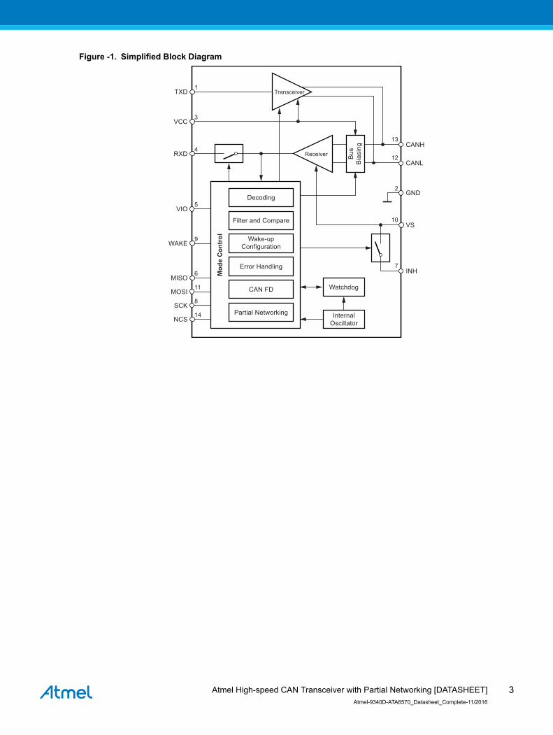
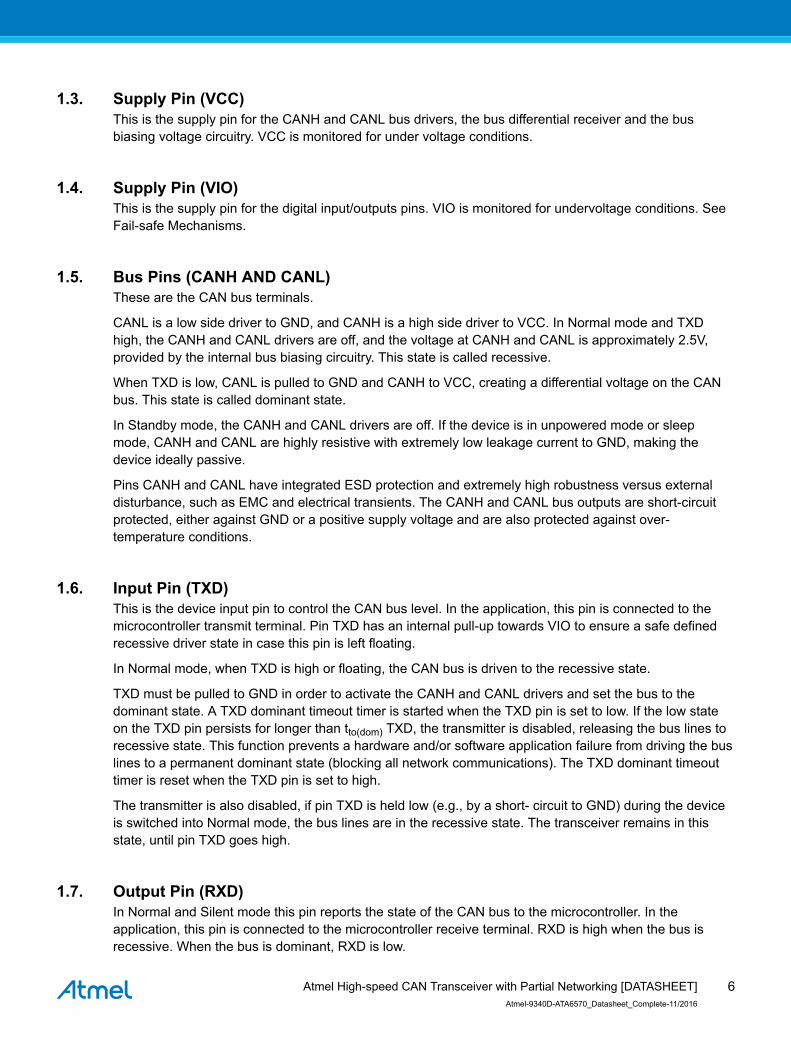
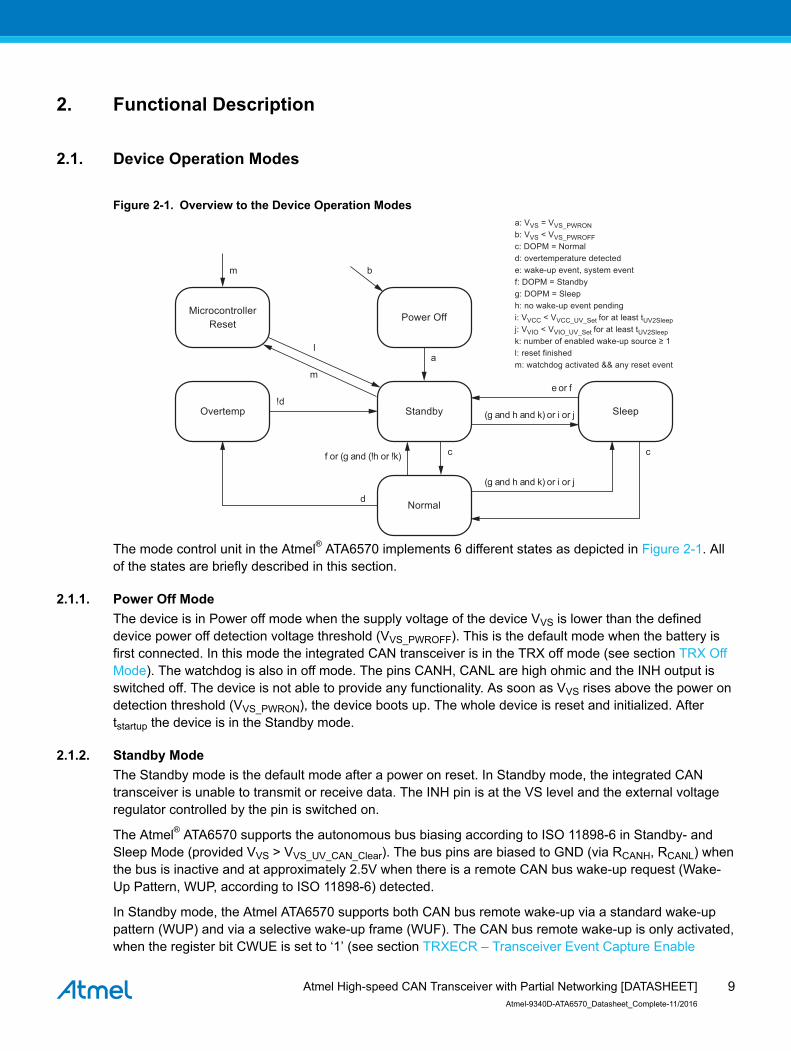
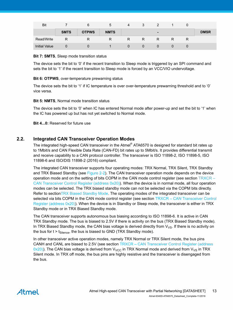
Bit 7 6 5 4 3 2 1 0
SMTS OTPWS NMTS - DMSR
ReadWrite R R R R R R R R
Initial Value 0 0 1 0 0 0 0 0
Bit 7 SMTS Sleep mode transition status
The device sets the bit to lsquo0rsquo if the recent transition to Sleep mode is triggered by an SPI command andsets the bit to lsquo1rsquo if the recent transition to Sleep mode is forced by an VCCVIO undervoltage
Bit 6 OTPWS over-temperature prewarning status
The device sets the bit to lsquo1rsquo if IC temperature is over over-temperature prewarning threshold and to lsquo0rsquovice versa
Bit 5 NMTS Normal mode transition status
The device sets the bit to lsquo0rsquo when IC has entered Normal mode after power-up and set the bit to lsquo1rsquo whenthe IC has powered up but has not yet switched to Normal mode
Bit 40 Reserved for future use
22 Integrated CAN Transceiver Operation ModesThe integrated high-speed CAN transceiver in the Atmelreg ATA6570 is designed for standard bit rates upto 1Mbits and CAN Flexible Data Rate (CAN-FD) bit rates up to 5Mbits It provides differential transmitand receive capability to a CAN protocol controller The transceiver is ISO 11898-2 ISO 11898-5 ISO11898-6 and ISODIS 11898-2 (2016) compliant
The integrated CAN transceiver supports four operating modes TRX Normal TRX Silent TRX Standbyand TRX Biased Standby (see Figure 2-2) The CAN transceiver operation mode depends on the deviceoperation mode and on the setting of bits COPM in the CAN mode control register (see section TRXCR ndashCAN Transceiver Control Register (address 0x20)) When the device is in normal mode all four operationmodes can be selected The TRX biased standby mode can not be selected via the COPM bits directlyRefer to sectionTRX Biased Standby Mode The operating modes of the integrated transceiver can beselected via bits COPM in the CAN mode control register (see section TRXCR ndash CAN Transceiver ControlRegister (address 0x20)) When the device is in Standby or Sleep mode the transceiver is either in TRXStandby mode or in TRX Biased Standby mode
The CAN transceiver supports autonomous bus biasing according to ISO 11898-6 It is active in CANTRX Standby mode The bus is biased to 25V if there is activity on the bus (TRX Biased Standby mode)In TRX Biased Standby mode the CAN bias voltage is derived directly from VVS If there is no activity onthe bus for t gt tSilence the bus is biased to GND (TRX Standby mode)
In other transceiver active operation modes namely TRX Normal or TRX Silent mode the bus pinsCANH and CANL are biased to 25V (see section TRXCR ndash CAN Transceiver Control Register (address0x20)) The CAN bias voltage is derived from VVCC in TRX Normal mode and derived from VVS in TRXSilent mode In TRX off mode the bus pins are highly resistive and the transceiver is disengaged fromthe bus
Atmel High-speed CAN Transceiver with Partial Networking [DATASHEET]Atmel-9340D-ATA6570_Datasheet_Complete-112016
13
Figure 2-2 Overview to the Integrated CAN TRX Operation Modes
TRX OffModeTX offRX off
RXD VIO levelCANHL tri-state
a Device in (Power Off or Overtemp or Reset mode) or VVS lt VVS_UV_CAN_Setb VVS gt VVS_UV_CAN_Clear and device not in Power Off and Overtemp mode
i DOPM = Normalj TXD = HIGH
l COPM = TRX Normal mode with 2rsquob01m COPM = TRX Normal mode with 2rsquob10n RXD recessive clamping detectedo VVCC has been smaller than VVCC_TX_Sd for tSUP_UV_filterp VVCC has been larger than or equal to VVCC_TX_Sd for tSUP_UV_filter
c Bus wake-up event or DOPM = Normal and COPM = TRX Normal with 2lsquob01 and VVCC has been smaller than VVCC_TX_Sd for tSUP_UV_filterd for t gt tsilence no bus activity detectede t lt tsilencef VVCC gt VVCC_UV_Set for tSUP_UV_filterg COPM = TRX Silent and DOPM = Normalh (DOPM = Sleep or Standby) or (DOPM = Normal and COPM = TRX Standby)
k VVCC lt VVCC_UV_Set for tSUP_UV_filter
b
a
all modes
a
i and [ (p and l) or m] and n and j
g or n
g or n
g or (i and [ (p and l)or m] and j)
d and (h or (k and I))
d and (h or (k and I))
i and [ (p and I) or m] and j
d and (h or k and I)
d and (h or k and I)
i and l and o
i and l and p
i and [ (p and I) or m] and j
(i and I and o) or(g and n)
g
d and h
e and h
TRX StandbyModeTX offRX off
RXD wake-upHighCANHL Ground
cd
TRX BiasedModeTX offRX off
RXD wake-upHighCANHL 25V (VS)
TRX SilentModeTX offRX on
RXD bit streamCANHL 25V (VS)
TRX NormalModeTX onRX on
RXD bit streamCANHL 25V (VCC)
TRX ReducedNormal Mode
TX offRX on
RXD bit streamCANHL 25V (VS)
221 TRX Off ModeThe CAN transceiver is completely switched off in the TRX Off mode The CAN bus pins CANH CANLare highly resistive and RXD pin is at the VIO level
As shown in Figure 2-2 the integrated CAN transceiver will enter the TRX Off mode in following cases
1 the device switches to Power off mode or2 the device switches to Overtemp mode or3 VVS falls below the CAN undervoltage detection threshold VVS_UV_CAN_Set
It will be switched on again and enter CAN TRX Standby mode when VVS rises above the CANundervoltage release threshold and the device is no longer in Power Off Overtemp mode
Atmel High-speed CAN Transceiver with Partial Networking [DATASHEET]Atmel-9340D-ATA6570_Datasheet_Complete-112016
14
222 TRX Standby ModeIn the TRX Standby mode the transmitter and the receiver are switched off to reduce currentconsumption The wake-up comparator monitors the bus lines for a valid remote bus wake-up pattern(WUP) provided CAN bus wake-up detection is enabled (CWUE=1) Two periods of dominant bus-levelsseparated by a period of recessive bus-level each of at least tFilter switches the RXD pin to low to signal awake-up request to the microcontroller Figure 2-3 describes the process and timing of the WUPdetection In the TRX Standby mode the bus lines are biased to ground to reduce current consumption toa minimum
Figure 2-3 Timing of CAN Standard Wake-Up via Wake-Up Pattern (WUP)
tdom = tFilter tdom = tFiltertrec = tFilter
t le tWake
VDiff
dominantCANH
CANL
RXD
recessive
Bus-wake-upis signalled
dominant
As shown in Figure 2-2 the CAN transceiver will enter the TRX Standby mode in following cases
1 when the device leaves Power off mode or Overtemp mode and sufficient VVS is applied or2 any of the conditions for CAN TRX Biased Standby mode are valid for longer than tSilence (see
section TRX Biased Standby Mode)
223 TRX Biased Standby ModeThe CAN transceiver behavior in the TRX Biased Standby mode is basically the same as in the TRXStandby mode The only difference is that in the TRX Biased Standby mode the bus pins are biased to25V The integrated CAN transceiver will enter this mode when activity is detected on the CAN bus whilethe transceiver is in TRX Standby mode The transceiver will return to TRX Standby mode if the CAN busis silent for longer than tSilence (see section WUP Detection and Bias Control)
As shown in Figure 2-2 the CAN transceiver will enter the TRX Biased Standby mode in following cases
1 From TRX SilentNormalReduced normal mode when tSilence time out is not detected and thedevice is in Standby (DOPM = 100) or Sleep mode (DOPM = 001) or
2 From TRX SilentNormalReduced normal mode when tSilence time out is not detected and thedevice is in Normal mode (DOPM = 111) and the COPM is set to TRX Standby mode (COPM = 00)or
3 From TRX NormalReduced normal mode (COPM = 01) when VCC lt VVCC_UV_Set is detected andtSilence time out is not detected or
4 From TRX Standby mode when the device is in Normal mode (DOPM = 111) COPM is set to TRXNormal mode (COPM = 01) and VCC lt VVCC_TX_Sd has been detected or
5 From TRX Standby mode when a wake-up event is detected on the CAN bus
Atmel High-speed CAN Transceiver with Partial Networking [DATASHEET]Atmel-9340D-ATA6570_Datasheet_Complete-112016
15
224 TRX Silent ModeThe TRX Silent mode is a receive-only mode of the CAN transceiver It can be used for instance to testthe connection of the bus medium or for the software-driven selective wake-up In the TRX Silent modethe device can still receive data from the bus but the transmitter is disabled and therefore no data can besent to the CAN bus The bus pins are released to recessive state All other IC functions continue tooperate as they do in the TRX Normal mode CAN biasing remains active Silent mode can be used toprevent a faulty CAN controller from disrupting all network communicationsAs shown in Figure 2-2 the CAN transceiver will enter the TRX Silent mode in following cases
1 the device is in Normal mode (DOPM = Normal) and CAN transceiver is in TRX Silent mode(COPM = TRX Silent)
2 the device is in Normal mode and CAN transceiver is in TRX Normal mode and a RXD recessiveclamping failure is detected
It will remain in TRX Silent mode if VCC undervoltage is detected or a RXD recessive clamping failure isdetected even if CAN TRX Normal mode is selected in device Normal mode
225 TRX Normal ModeIn the TRX Normal mode the integrated transceiver is able to transmit and receive data via the CANH andCANL bus lines The output driver stage is active and drives data from the TXD input to the CAN bus Thereceiver converts the analog data on the bus lines into digital data which is output to pin RXD The busbiasing is set to VVCC2 and the undervoltage monitoring of VVCC is active
The slope of the output signals on the bus lines is controlled and optimized in a way that guarantees thelowest possible electromagnetic emission (EME)
As shown in Figure 2-2 the CAN transceiver will enter the TRX Normal mode in following cases
1 the device is in Normal mode (DOPM = Normal) AND the CAN transceiver has been enabled bysetting bits COPM to lsquo01rsquo or lsquo10rsquo AND no VCC undervoltage is detected AND no RXD recessiveclamping is detected
2 the transceiver is in the TRX Reduced Normal mode and VVCC gt VVCC_TX_Sd for t gt tSUP_UV_filter
If pin TXD is held low (eg by a short-circuit to GND) when CAN TRX Normal mode is selected via bitsCOPM the transceiver will not enter CAN TRX Normal mode but will switch to or remain in TRX Silentmode It will remain in TRX Silent mode until pin TXD goes high in order to prevent a hardware andorsoftware application failure from driving the bus lines to an unwanted dominant state
The application can determine whether the CAN transceiver is ready to transmit data or is disabled byreading the CAN Transmitter Status bit (TXS) bit in the Transceiver Status Register (see section TRXSRndash CAN Transceiver Status Register (address 0x22))
226 TRX Reduced Normal ModeIn the TRX Reduced Normal mode the transmitter is switched off as VCC is lower than the VVCC_TX_Sdthreshold All other features available in the TRX Normal mode is also provided in the TRX ReducedNormal mode
As shown in Figure 2-2 the CAN transceiver will enter the TRX Reduced Normal mode when thetransceiver is in TRX Normal mode and VVCC lt VVCC_TX_Sd for t gt tSUP_UV_filter
Atmel High-speed CAN Transceiver with Partial Networking [DATASHEET]Atmel-9340D-ATA6570_Datasheet_Complete-112016
16
227 Related Registers
2271 TRXCR ndash CAN Transceiver Control Register (address 0x20)
Bit 7 6 5 4 3 2 1 0
- CFDPE PNCFOK CPNE - - COPM[10] TRXCR
Read Write R RW RW RW R R RW RW
Initial Value 0 1 0 0 0 0 0 1
Bit 7 Reserved for future use
Bit 6 CFDPE The external microcontroller should set the bit to lsquo1rsquo to enable the CAN FD passive featurewhen selective wake-up is activated should set the bit to lsquo0rsquo vice versa The bit is set to 1 by default afterpower on reset The bit shall be set to 1 for continuous sending dom-rec bits with a bitrate higher than1Mbits
Bit 5 PNCFOK The external microcontroller should set the bit to lsquo1rsquo after successfully configuring thepartial networking registers and to lsquo0rsquo vice versa In addition the device will reset the bit to 0automatically after any write access to the partial networking configuration related registers
Bit 4 CPNE The external microcontroller should set the bit to lsquo1rsquo to enable selective wake-up and to lsquo0rsquovice versa
Bit 32 Reserved for future use
Bit 10 COPM (The TRXCR register is a control register Therefore the state of the transceiver will notbe mirrored to this register COPM bit only defines the expected state of the transceiver when the deviceis switched to Normal mode The finite state machine in Figure 2-2 will not change the COPM bits) [10] ndashSelect CAN Transceiver operation mode
COPM[10] CAN TRX Operation Mode
2rsquob00 TRX Standby mode
2rsquob01
TRX Normal mode (when DOPM = Normal) VCC undervoltage detectionactive for the transceiver finite state machine The transceiver switches to theTRX biased Standby mode immediately after detecting the VCCundervoltage
2rsquob10
TRX Normal mode (when DOPM = Normal) VCC undervoltage detectioninactive for the transceiver finite state machine The transceiver switches fromTRX NormalReduced Normal mode to TRX biased Standby mode when thedevice is forced to Sleep mode by a VCC undervoltage event
2rsquob11 TRX Silent mode
Atmel High-speed CAN Transceiver with Partial Networking [DATASHEET]Atmel-9340D-ATA6570_Datasheet_Complete-112016
17
2272 TRXSR ndash CAN Transceiver Status Register (address 0x22)
Bit 7 6 5 4 3 2 1 0
TXS PNERRS PNCFS PNOSCS CBSS - VCCS TXDOUT TRXSR
ReadWrite R R R R R R R R
Initial Value 0 1 0 0 1 0 0 0
Bit 7 TXS Transmitter status the device sets the bit to lsquo1rsquo if the transmitter is ready to transmit data andto lsquo0rsquo if CAN transmitter is disabled
Bit 6 PNERRS Partial networking error detection status the device sets the bit to lsquo0rsquo if no CAN partialnetworking error detected (PNEFD = 0 ampamp PNCFOK = 1 ampamp no oscillator hardware failure detected(default)) to lsquo1rsquo vice versa (PNEFD = 1 || PNCFOK = 0)
Bit 5 PNCFS Partial networking configuration status the device sets the bit to lsquo0rsquo if partial networkingconfiguration error is detected (PNCFOK = 0) to lsquo1rsquo vice versa
Bit 4 PNOSCS Partial networking oscillator ok the device sets the bit to lsquo1rsquo if CAN partial networkingoscillator is running at target frequency to lsquo0rsquo vice versa
Bit 3 CBSS Bus status the device sets the bit to lsquo1rsquo if CAN bus is inactive (for longer than tSilence) to lsquo0rsquovice versa
Bit 2 Reserved for future use
Bit 1 VCCS VVCC status the device sets the bit to lsquo1rsquo if VVCC is below the undervoltage detectionthreshold to lsquo0rsquo vice versa
Bit 0 TXDOUT TXD time out status the device sets the bit to lsquo1rsquo if CAN transmitter is disabled due to aTXD dominant timeout event to lsquo0rsquo if no TXD dominant timeout event was detected
2273 BFIR - Bus Failure Indication Register (address 0x33)
Bit 7 6 5 4 3 2 1 0
- - - - - - BOUT BSC BFIR
Read Write R R R R R R R R
Initial Value 0 0 0 0 0 0 0 0
Bit 72 Reserved for future use
Bit 1 BOUT bus dominant timeout event indicator the BOUT bit shows the current status of the busdominant timeout detection If the bit reads lsquo1rsquo the bus is currently in dominant timeout state otherwisethe bit reads lsquo0rsquo
Bit 0 BSC bus short-circuit event capture indicator the BSC bit shows the current status of the busshort-circuit event detection If the bit reads lsquo1rsquo the bus is currently in short-circuit state otherwise the bitreads lsquo0rsquo
Atmel High-speed CAN Transceiver with Partial Networking [DATASHEET]Atmel-9340D-ATA6570_Datasheet_Complete-112016
18
2274 TRXESR2 ndash Transceiver Event Status Register 2 (address 0x35)
Bit 7 6 5 4 3 2 1 0
- - - - - - - RXDRCS TRXESR2
Read Write R R R R R R R R
Initial Value 0 0 0 0 0 0 0 0
Bit 71 Reserved for future use
Bit 0 RXDRCS RXD recessive clamping status the device sets the bit to lsquo1rsquo if the event is enabled in theTRXECR2 register and a RXD recessive clamping event is detected The bit is reset to lsquo0rsquo by the deviceeither when the device enters sleep or standby or unpowered mode or the RXD pin shows dominantagain
23 Wake-up in ATA6570
231 Local Wake-up via Pin WAKEThe device provides the high voltage WAKE input pin that can be used to wake up the device It is anedge sensitive pin (low to-high or high to low transition) Thus even if the WAKE pin is at high or lowvoltage it is possible to switch the IC into the Sleep mode It is usually connected to the ignition forgenerating a local wake-up in the application if the ignition is switched on
A glitch suppression circuit is integrated to avoid unexpected wake-up on the Wake pin The voltage onthe pin is detected as stable only when the level remains stable for tlocal_wu Therefore a local wake-uprequest is detected when the logic level on the pin WAKE has been already stable for at least tlocal_wu andthe new level remains stable for at least tlocal_wu
Local wake-up via pin WAKE can be enableddisabled via the register bits LWUFE and LWURE (seesection WKECR ndash WAKE Event Capture Enable Register (address 0x4C)) and the logic level at pinWAKE can be read via the register PWKS (see section PWKS ndash Pin WAKE Status Register (address0x4B)) if a valid interface voltage VVIO is provided
To reduce the battery current during low-power mode the Wake pin has internal pull-uppull-down currentsthat are activated when a stable level at the wake pin has been detected
bull High level on pin is followed by an internal pull up towards VSbull Low level is followed by an internal pull down towards GND
Local wake-up can only be activated in Standby and Sleep mode In Normal mode the status of thevoltage on pin WAKE can always be read via bit PWKVS Otherwise PWKVS is only valid if local wake-up is enabled In applications that donrsquot make use of the local wake-up facility local wake-up should be disabled and theWAKE pin should be connected to GND to ensure optimal EMI performance
232 Remote Wake-up Pattern according to ISO 11898-5 (Partial Networking Disabled)If the CAN transceiver is in TRX Standby mode and CAN bus wake-up is enabled (CWUE = 1) but CANselective wake-up is disabled (CPNE = 0 or PNCFOK = 0) the device will monitor the bus for a standardwake-up pattern as specified in ISO11898-5
This filtering helps to avoid spurious wake-up events which could be triggered by for example adominant clamped bus or by dominant phases due to noise spikes on the bus transients or EMI
Atmel High-speed CAN Transceiver with Partial Networking [DATASHEET]Atmel-9340D-ATA6570_Datasheet_Complete-112016
19
The wake-up pattern consists of multiple consecutive dominant bus levels for a duration of at least tFiltereach separated by a recessive bus level with a duration of at least tFilter Dominant or recessive bits in-between the above mentioned phases which are shorter than tFilter are ignored
The complete dominant-recessive-dominant pattern as shown in Figure 2-3 must be received withintWake to be recognized as a valid wake-up pattern Otherwise the internal wake-up logic is reset Thecomplete wake-up pattern will then need to be retransmitted to trigger a wake-up event
When a valid CAN WUP is detected on the bus the wake-up bit CWUS in the transceiver event statusregister is set (see section TRXESR ndash Transceiver Event Status Register (address 0x63)) and pin RXD isdriven low If the device was in Sleep mode when the wake-up event was detected it will switch pin INHto VS to activate external voltage regulators (eg for supplying VCC and VIO) and enter Standby mode
CAN wake-up via WUP can only be disabled via bit CWUE If CWUE is set to lsquo0rsquo no remote wake-up viathe CAN bus is possible In case CWUE is set to lsquo1rsquo and selective wake-up is disabled the device willswitch to Standby mode after detecting the wake-up pattern (WUP) coming from Sleep mode In caseCWUE is set to lsquo1rsquo and the selective wake-up is enabled the device will first switch on the bus biasingafter detecting the WUP and will only switch afterwards to the Standby mode when it detects a validWUF (please refer to the next section for WUF)
233 Remote Wake-up Frame according to ISO 11898-6
2331 CAN Selective Wake-upPartial networking makes it possible for a CAN node or a CAN sub-network to be woken up individually bymeans of dedicated and predefined frames the so called wake-up frames (WUF) When a particularnodersquos tasks are not required it is in selective sleep mode
The transceiver monitors the bus for dedicated CAN wake-up frames when both CAN wake-up (CWUE =lsquo1rsquo) and CAN selective wake-up (CPNE = lsquo1rsquo) are enabled and the partial networking registers areconfigured correctly (PNCFOK = lsquo1rsquo) An accurate oscillator and a low power high speed comparator arerunning in this case to support the correct detection of the wake-up frame
According to ISO11898-1 a wake-up frame is a CAN frame consisting of an identifier field (ID) a DataLength Code (DLC) a data field and a Cyclic Redundancy Check (CRC) code including the CRCdelimiter
The wake-up CAN frame (ID and data) is fully configurable via SPI communication A standard (11-bit) orextended (29-bit) identifier for the wake-up frame format can be selected via bit IDE in the Frame controlregister CFCR (see section CFCR - CAN Frame Configuration Register (address 0x2F))
In the ID registers (see section CIDR0 - CAN ID Register 0 (address 0x27) to section CIDR3 - CAN IDRegister 3 (address 0x2A)) a valid WUP can be defined and stored To allow a group of identifiers to berecognized as valid by an individual node an ID mask (see section CIDMR0 - CAN ID Mask Register 0(address 0x2B) to section CIDMR3 - CAN ID Mask Register 3 (address 0x2E)) can be defined in themask registers where a 1 means lsquodont carersquo
A single wake-up frame can wake up multiple groups of nodes by comparing the incoming data field withthe data mask as the data field indicates which nodes are to be woken up Groups of nodes can be pre-defined and associated with bits in a data mask
The number of data bytes expected in the data field of a CAN wake-up frame are set with the data lengthcode (bits DLC in the frame control register in section CFCR - CAN Frame Configuration Register(address 0x2F)) If DLC ne 0000 (one or more data bytes expected) at least one bit in the data field of thereceived wake-up frame must be set to 1 and at least one equivalent bit in the associated data maskregister in the transceiver (register for data mask to be defined) must also be set to 1 for a successful
Atmel High-speed CAN Transceiver with Partial Networking [DATASHEET]Atmel-9340D-ATA6570_Datasheet_Complete-112016
20
wake-up Each matching pair of logic 1s indicates a group of nodes to be activated (since the data field isup to 8 bytes long up to 64 groups of nodes can be defined)
If DLC = 0000 a node will wake up if the WUF contains a valid identifier and the received data lengthcode is 0000 regardless of the values stored in the data mask If DLC ne 0000 and all data mask bits areset to 0 the device cannot be woken up via the CAN bus (note that all data mask bits are 1 per default) Ifa WUF contains a valid ID but the DLCs (in the Frame control register and in the WUF) donrsquot match thedata field is ignored and no nodes will be woken up The data length code and the data field can beexcluded from the evaluation of the wake-up frame If bit PNDM = 0 (see section CFCR - CAN FrameConfiguration Register (address 0x2F)) only the identifier field is evaluated to determine if the framecontains a valid wake-up frame If PNDM = 1 (the default value) the data field is included as part of thewake-up filtering
When PNDM = 0 a valid wake-up frame is detected and a wake-up event is captured (and CWUS is setto 1) when
bull the identifier field in the received wake-up frame matches the pattern in the ID registers afterfiltering AND
bull the CRC field in the received frame (including a recessive CRC delimiter) was received withouterror
When PNDM = 1 a valid wake-up frame is detected whenbull the identifier field in the received wake-up frame matches the pattern in the ID registers after
filtering ANDbull the frame is not a Remote frame ANDbull the data length code in the received frame matches the configured data length code (bits DLC)
ANDbull if the data length code is greater than 0 at least one bit in the data field of the received frame is set
and the corresponding bit in the associated data mask register is also set ANDbull the CRC field in the received frame (including a recessive CRC delimiter) was received without
error
The internal error counter will be incremented when an erroneous CAN frame (eg a lsquostuffingrsquo error) isreceived prior the ACK field If a CAN frame is received without any errors appearing in front of the ACKfield the counter will be decremented Any data received after the CRC delimiter and before the nextSOF will be ignored by the partial networking module If the counter overflows (FEC gt ERRCNT seesection EFCR - Error Frame Counter Threshold Register (address 0x3A)) a frame detect error iscaptured (PNEFD = 1 see section TRXESR ndash Transceiver Event Status Register (address 0x63)) and thedevice wakes up the counter is reset to zero when the bias is switched off and partial networking is re-enabled
If partial networking is assumed to be configured correctly the PNCFOK has to be set to 1 by theapplication software The PNCFOK will be cleared after a write access to any of the CAN partialnetworking configuration registers (see section DRCR - Data Rate Configuration Register (address 0x26)to CDMR07 - CAN Data Mask Registers 07 (address 0x68hellip0x6F))
Any valid wake-up pattern (according to ISO 11898-5-6) will trigger a wake- up event if selective wake-up is disabled (CPNE = 0) or partial networking is not configured correctly (PNCFOK = 0) and the CANtransceiver is in TXD Standby mode with wake-up enabled (CWUE = 1)
All wake-up patterns will be ignored if the CAN transceiver is in TRX NormalSilent mode or CAN wake-up is disabled (CWUE = 0)
Atmel High-speed CAN Transceiver with Partial Networking [DATASHEET]Atmel-9340D-ATA6570_Datasheet_Complete-112016
21
2332 CAN Selective Wake-up and CAN FDCAN Flexible Data-rate (CAN FD) is an improved CAN protocol in regards of bandwidth and payload Asspecified in ISO 11898-1 CAN FD is based on the CAN protocol and still uses the CAN bus arbitrationmethod However after the arbitration phase of a classical CAN frame the data rate is increased and thedata bits are transferred with a higher bit rate than in the arbitration phase and returns to the longer bittime at the CRC Delimiter before the receivers transmit their acknowledge bits Besides the increased bitspeed the new CAN FD allows date frames up to 64 bytes compared with the maximum of 8 bytes withclassical CAN
The Atmelreg ATA6570 can be configured to recognize CAN FD frames as valid frames When CFDPE = 1the error counter is decremented every time the control field of a CAN FD frame is received The deviceremains in Sleep mode (CAN FD-passive) with partial networking enabled CAN FD frames are neverrecognized as valid wake-up frames even if PNDM = 0 and the frame contains a valid ID After receivingthe control field of a CAN FD frame the device ignores further bus signals until idle is again detected
When CFDPE is set to 0 CAN FD frames are interpreted as frames with errors by the partial networkingmodule So the error counter is incremented when a CAN FD frame is received Bit PNEFD is set to 1and the device wakes up if the ratio of CAN FD frames to valid CAN frames exceeds the threshold thattriggers error counter overflow
In the presence of CAN FD frames the transceivers can behave as followsbull Non-FD (Only Classical CAN frames) Systematically disturbs CAN- FD frames (eg through
error frames) or wakes up or terminates reception (eg Bus Off) when all or some frames presenton the bus are CAN-FD frames
bull CAN FD silent Capable of receiving defined configurable Classical CAN frames while underdefined conditions successfully ignoring all CAN-FD frames when interleaved with Classical CANframes
bull CAN FD passive Capable of transmitting and receiving all Classical CAN frames while underdefined conditions successfully ignoring all FD frames when interleaved with Classical CAN frames
bull CAN FD active Capable of successfully transmitting and receiving CAN FD frames and ClassicalCAN frames in an interleaved fashion
The Atmel ATA6570 device can be configured into all four modes in order to serve best the givenapplication
234 Wake-up via SPIIn case of an SPI command while the system is in a low power mode but with enabled SPI interface thedevice shall be woken up and enter the operation mode issued together with the SPI command A SPIcommand failure for instance invalid length of SPI command write access to read-only register and etcwill also trigger an interrupt event of the device (see Table 2-3)
235 Related Registers for Configuring the CAN Partial Networking
2351 DRCR - Data Rate Configuration Register (address 0x26)
Bit 7 6 5 4 3 2 1 0
- - - - - DR[20] DRCR
Read Write R R R R R RW RW RW
Initial Value 0 0 0 0 0 1 0 1
Bit 74 Reserved for future use
Atmel High-speed CAN Transceiver with Partial Networking [DATASHEET]Atmel-9340D-ATA6570_Datasheet_Complete-112016
22
Bit 20 DR[20] ndash Select CAN data rate
DR[20] CAN Data Rate (Kbits)
3rsquob000 50
3rsquob001 100
3rsquob010 125
3rsquob011 250
3rsquob100 Reserved (intended for future use currently selects 500Kbits)
3rsquob101 500
3rsquob110 Reserved (intended for future use currently selects 500Kbits)
3rsquob111 1000
2352 CIDR0 - CAN ID Register 0 (address 0x27)
Bit 7 6 5 4 3 2 1 0
ID0[70] CIDR0
ReadWrite RW RW RW RW RW RW RW RW
Initial Value 0 0 0 0 0 0 0 0
Bit 70 ID0 bits ID07 to ID00 of the extended frame format
2353 CIDR1 - CAN ID Register 1 (address 0x28)
Bit 7 6 5 4 3 2 1 0
ID1[70] CIDR1
ReadWrite RW RW RW RW RW RW RW RW
Initial Value 0 0 0 0 0 0 0 0
Bit 70 ID1 bits ID15 to ID08 of the extended frame format
2354 CIDR 2 - CAN ID Register 2 (address 0x29)
Bit 7 6 5 4 3 2 1 0
ID2[70] CIDR2
ReadWrite RW RW RW RW RW RW RW RW
Initial Value 0 0 0 0 0 0 0 0
Bit 72 ID2 bits ID23 to ID18 of the extended frame format bits ID05 to ID00 of the standard frameformat
Bit 10 ID2 bits ID17 to ID16 of the extended frame format
Atmel High-speed CAN Transceiver with Partial Networking [DATASHEET]Atmel-9340D-ATA6570_Datasheet_Complete-112016
23
2355 CIDR3 - CAN ID Register 3 (address 0x2A)
Bit 7 6 5 4 3 2 1 0
- - - ID3[40] CIDR3
Read Write R R R RW RW RW RW RW
Initial Value 0 0 0 0 0 0 0 0
Bit 75 Reserved for future use
Bit 40 ID3 bits ID28 to ID24 of the extended frame format bits ID10 to ID06 of the standard frameformat
2356 CIDMR0 - CAN ID Mask Register 0 (address 0x2B)
Bit 7 6 5 4 3 2 1 0
IDM0[70] CIDMR0
ReadWrite RW RW RW RW RW RW RW RW
Initial Value 0 0 0 0 0 0 0 0
Bit 70 IDM0 Mask bits ID07 to ID00 of the extended frame format 1 means lsquodont carersquo
2357 CIDMR1 - CAN ID Mask Register 1 (address 0x2C)
Bit 7 6 5 4 3 2 1 0
IDM1[70] CIDMR1
ReadWrite RW RW RW RW RW RW RW RW
Initial Value 0 0 0 0 0 0 0 0
Bit 70 IDM1 Mask bits ID15 to ID08 of the extended frame format 1 means lsquodont carersquo
2358 CIDMR2 - CAN ID Mask Register 2 (address 0x2D)
Bit 7 6 5 4 3 2 1 0
IDM2[70] CIDMR2
ReadWrite RW RW RW RW RW RW RW RW
Initial Value 0 0 0 0 0 0 0 0
Bit 72 IDM2 Mask bits ID23 to ID18 of the extended frame format bits ID05 to ID00 of the standardframe format
Bit 10 IDM2 Mask bits ID17 to ID16 of the extended frame format 1 means lsquodont carersquo
2359 CIDMR3 - CAN ID Mask Register 3 (address 0x2E)
Bit 7 6 5 4 3 2 1 0
- - - IDM3[40] CIDMR3
Read Write R R R RW RW RW RW RW
Initial Value 0 0 0 0 0 0 0 0
Bit 75 Reserved for future use
Atmel High-speed CAN Transceiver with Partial Networking [DATASHEET]Atmel-9340D-ATA6570_Datasheet_Complete-112016
24
Bit 40 IDM3 Mask bits ID28 to ID24 of the extended frame format bits ID10 to ID06 of the standardframe format 1 means lsquodont carersquo
23510 CFCR - CAN Frame Configuration Register (address 0x2F)
Bit 7 6 5 4 3 2 1 0
IDE PNDM - - DLC[30] CFCR
Read Write RW RW R R RW RW RW RW
Initial Value 0 1 0 0 0 0 0 0
Bit 7 IDE Identifier format the external microcontroller should set the bit to lsquo1rsquo if identifier is in extendedframe format (29-bit) set to lsquo0rsquo if identifier is in standard frame format (11-bit)
Bit 6 PNDM Partial networking data mask the external microcontroller should set the bit lsquo1rsquo if data lengthcode and data field are evaluated at wake-up set to lsquo0rsquo if data length code and data field are lsquodonrsquot carersquofor wake-up
Bit 54 Reserved for future use
Bit 30 DLC[30] Data length configuration select number of data bytes expected in a CAN frame
DLC[30] Number of Data Bytes
4rsquob0000 0
4rsquob0001 1
4rsquob0010 2
4rsquob0011 3
4rsquob0100 4
4rsquob0101 5
4rsquob0110 6
4rsquob0111 7
4rsquob1000 8
4rsquob1001 to 4rsquob1111 Tolerated 8 bytes expected DM0 (data mask 0) ignored
23511 EFCR - Error Frame Counter Threshold Register (address 0x3A)
Bit 7 6 5 4 3 2 1 0
- - - EERCNT EFCR
ReadWrite R R R RW RW RW RW RW
Initial Value 0 0 0 1 1 1 1 1
Bit 75 Reserved for future use
Bit 40 Set the error frame counter overflow threshold If the counter overflows (counter gt ERRCNT) aframe detect error is captured (PNEFD = 1) and the device wakes up
Atmel High-speed CAN Transceiver with Partial Networking [DATASHEET]Atmel-9340D-ATA6570_Datasheet_Complete-112016
25
23512 FECR ndash Failure Error Counter Register (address 0x3B)
Bit 7 6 5 4 3 2 1 0
- - - FEC FECR
ReadWrite R R R RW RW RW RW RW
Initial Value 0 0 0 0 0 0 0 0
Bit 75 Reserved for future use
Bit 40 If the device receives a CAN frame containing errors (eg a lsquostuffingrsquo error) that are received inadvance of the ACK field an internal error counter is incremented If a CAN frame is received without anyerrors appearing in front of the ACK field the counter is decremented Data received after the CRCdelimiter and before the next SOF is ignored by the partial networking module If the counter overflows(FEC gt ERRCNT see section FECR ndash Failure Error Counter Register (address 0x3B)) a frame detecterror is captured (PNEFD = 1 see section TRXESR ndash Transceiver Event Status Register (address 0x63))and the device wakes up the counter is reset to zero when the bias is switched off and partial networkingis re-enabled
23513 GLFT ndash Glitch Filter Threshold Register (address 0x67)
Bit 7 6 5 4 3 2 1 0
- - - - - GLF[20] GLFT
Read Write R R R R R RW RW RW
Initial Value 0 0 0 0 0 0 1 0
Bit 73 Reserved for future use
Bit 20 Set the glitch filter threshold from 5 to 55 of the arbitration bit rate
GLF[20] samples(le500Kbits) samples(1Mbits)
3rsquob000 1 [lt242lt517] 1 [lt483lt1035]]
3rsquob001 2 [lt483lt776] 2 [lt966lt1552]
3rsquob010 3 [lt725lt1035] 3 [lt1449lt207]]
3rsquob011 4 [lt966lt1294] 4 [lt1932lt2087]
3rsquob100 5 [lt1208lt1552] 5 [lt2415lt3105]
3rsquob101 6 [lt1449lt1811] 6 [lt2899lt3622]
3rsquob110 7 [lt1691lt207] 7 [lt3382lt4140]
3rsquob111 24 [lt5797lt6469] 13 [lt628lt7245]
Assumption clock tolerance plusmn3 transmitter plusmn05 tolerance OSR(le500Kbits) = 40 OSR(1Mbits) = 20
Atmel High-speed CAN Transceiver with Partial Networking [DATASHEET]Atmel-9340D-ATA6570_Datasheet_Complete-112016
26
23514 CDMR07 - CAN Data Mask Registers 07 (address 0x68hellip0x6F)
Bit 7 6 5 4 3 2 1 0
DM0hellip7[70] CDMR
ReadWrite RW RW RW RW RW RW RW RW
Initial Value 1 1 1 1 1 1 1 1
Bit 70 DM0hellip7[70] data mask 0hellip7 configuration
Table 2-2 Data Mask and the CAN Data Filed
CAN frame DLC Byte 0 Byte 1 Byte 2 Byte 3 Byte 4 Byte 5 Byte 6 Byte 7 CRC
Data mask DLC gt 8 DM0 DM1 DM2 DM3 DM4 DM5 DM6 DM7 CRC
CAN frame DLC Byte 0 Byte 1 Byte 2 Byte 3 Byte 4 Byte 5 Byte 6 Byte 7 CRC
Data mask DLC = 8 DM0 DM1 DM2 DM3 DM4 DM5 DM6 DM7 CRC
CAN frame DLC Byte 0 Byte 1 Byte 2 Byte 3 Byte 4 Byte 5 Byte 6 Byte 7 CRC
Data mask DLC = 7 DM1 DM2 DM3 DM4 DM5 DM6 DM7 CRC
CAN frame DLC Byte 0 Byte 1 Byte 2 Byte 3 Byte 4 Byte 5 Byte 6 CRC
Data mask DLC = 6 DM2 DM3 DM4 DM5 DM6 DM7 CRC
CAN frame DLC Byte 0 Byte 1 Byte 2 Byte 3 Byte 4 Byte 5 CRC
Data mask DLC = 5 DM3 DM4 DM5 DM6 DM7 CRC
CAN frame DLC Byte 0 Byte 1 Byte 2 Byte 3 Byte 4 CRC
Data mask DLC = 4 DM4 DM5 DM6 DM7 CRC
CAN frame DLC Byte 0 Byte 1 Byte 2 Byte 3 CRC
Data mask DLC = 3 DM5 DM6 DM7 CRC
CAN frame DLC Byte 0 Byte 1 Byte 2 CRC
Data mask DLC = 2 DM6 DM7 CRC
CAN frame DLC Byte 0 Byte 1 CRC
Data mask DLC = 1 DM7 CRC
CAN frame DLC Byte 0 CRC
DM x
Bit 7 Bit 6 Bit 5 Bit 4 Bit 3 Bit 2 Bit 1 Bit 0
Byte x
Bit 7 Bit 6 Bit 5 Bit 4 Bit 3 Bit 2 Bit 1 Bit 0
Atmel High-speed CAN Transceiver with Partial Networking [DATASHEET]Atmel-9340D-ATA6570_Datasheet_Complete-112016
27
23515 BFECR - Bus Failure Event Capture Enable Register (address 0x32)
Bit 7 6 5 4 3 2 1 0
- - - - - - BOUTE BSCE BFECR
Read Write R R R R R R RW RW
Initial Value 0 0 0 0 0 0 0 0
Bit 72 Reserved for future use
Bit 1 BOUTE bus dominant timeout event capture enable the BOUTE bit must be set to lsquo1rsquo to enablethe bus dominant timeout detection Setting the bit to `0` disables the bus dominant timeout detection
Bit 0 BSCE bus short-circuit event capture enable the BSCE bit must be set to lsquo1rsquo to enable the busshort-circuit event detection Setting the bit to `0` disables the bus short-circuit event detection
23516 PWKS ndash Pin WAKE Status Register (address 0x4B)
Bit 7 6 5 4 3 2 1 0
- - - - - - PWKVS - PWKS
Read Write R R R R R R R R
Initial Value 0 0 0 0 0 0 0 0
Bit 72 Reserved for future use
Bit 1 PWKVS Pin WAKE voltage status the device sets the bit to lsquo1rsquo if WAKE is high to lsquo0rsquo if WAKE islow PWKVS is always ldquo0rdquo in power-down mode if local wake-up is disabled
Bit 0 Reserved for future use
23517 GESR ndash Global Event Status Register (address 0x60)
Bit 7 6 5 4 3 2 1 0
OSCS - BFES - WKES TRXES - SYSES GESR
Read Write R R R R R R R R
Initial Value 0 0 0 0 0 0 0 1
Bit 7 System oscillator status the device sets the bit to lsquo1rsquo if a hardware failure of the system oscillator isdetected and sets the bit to lsquo0rsquo when the system oscillator is disabled for power saving purpose or thehardware failure disappeared after the oscillator is enabled (for instance in device Normal mode)
Bit 6 Reserved for future use
Bit 5 Bus failure event status the device sets the bit to lsquo1rsquo if there is bus failure event pending (any bit inthe BFESR register is lsquo1rsquo) The bit reads lsquo0rsquo if all status bits in the BFESR register are cleared
Bit 4 Reserved for future use
Bit 3 WKES WAKE event status the device sets the bit to lsquo1rsquo if there is a wake pin event pending (any bitin the WKESR register is lsquo1rsquo) The bit reads lsquo0rsquo if all status bits in the WKESR register are cleared
Atmel High-speed CAN Transceiver with Partial Networking [DATASHEET]Atmel-9340D-ATA6570_Datasheet_Complete-112016
28
Bit 2 TRXES Transceiver event status the device sets the bit to lsquo1rsquo if there is a transceiver event pending(any bit in the TRXESR register is lsquo1rsquo) The bit reads lsquo0rsquo if all status bits in the TRXESR register arecleared
Bit 1 Reserved for future use
Bit 0 SYSES System event status the device sets the bit to lsquo1rsquo if there is a system event pending (any bitin the SESR register is lsquo1rsquo) The bit reads lsquo0rsquo if all status bits in the SESR register are cleared
23518 SESR ndash System Event Status Register (address 0x61)
Bit 7 6 5 4 3 2 1 0
- - - PWRONS - OTPW SPIFS - ESR
Read Write R R R RW R RW RW R
Initial Value 0 0 0 1 0 0 0 0
Bit 75 Reserved for future use
Bit 4 PWRONS Power on status the device sets the bit to lsquo1rsquo if the device has left Power off mode afterpower-on The bit can be reset to lsquo0rsquo by writing a lsquo1rsquo to the bit PWRONS is also cleared when the deviceis forced to sleep mode due to an undervoltage event The information stored in PWRONS could be lostin this case Bit NMTS in the Device Mode Status Register (DMSR) which is set to 0 when the deviceswitches to normal mode after power-on compensates for this
Bit 3 Reserved for future use
Bit 2 OTPW Overtemperature prewarning status the device sets the bit to lsquo1rsquo if the event is enabled inthe SECR register and the chip temperature has exceeded the overtemperature prewarning thresholdThe bit can be reset to lsquo0rsquo by writing a lsquo1rsquo to the bit OTPW is also cleared when the device is forced tosleep mode due to an undervoltage event
Bit 1 SPIFS SPI failure status the device sets the bit to lsquo1rsquo if the event is enabled in the SECR registerand an SPI failure is detected The bit can be reset to lsquo0rsquo by writing a lsquo1rsquo to the bit SPIFS is also clearedwhen the device is forced to sleep mode due to an undervoltage event
Bit 0 Reserved for future use
23519 TRXESR ndash Transceiver Event Status Register (address 0x63)
Bit 7 6 5 4 3 2 1 0
- - PNEFD BS - - TRXF CWUS TRXESR
Read Write R RW RW RW R R RW RW
Initial Value 0 0 0 0 0 0 0 0
Bit 76 Reserved for future use
Bit 5 PNEFD Partial networking frame detection status the device sets the bit to lsquo1rsquo if a partialnetworking frame detection error is detected (error counter overflow) The bit can be reset to lsquo0rsquo by writinga lsquo1rsquo to the bit PNEFD is also cleared when the device is forced to sleep mode due to an undervoltageevent
Atmel High-speed CAN Transceiver with Partial Networking [DATASHEET]Atmel-9340D-ATA6570_Datasheet_Complete-112016
29
Bit 4 BS Bus status the device sets the bit to lsquo1rsquo if the event is enabled in the TRXECR register and noactivity on CAN bus is detected for tSilence The bit can be reset to lsquo0rsquo by writing a lsquo1rsquo to the bit BS is alsocleared when the device is forced to sleep mode due to an undervoltage event
Bit 32 Reserved for future use
Bit 1 TRXF Transceiver failure status the device sets the bit to lsquo1rsquo if the event is enabled in the TRXECRregister and a CAN failure event was detected The bit can be reset to lsquo0rsquo by writing a lsquo1rsquo to the bit TRXFis also cleared when the device is forced to sleep mode due to an undervoltage eventTRXF is triggered if
bull TXD is clamped dominant and system is in TRX Normal modebull a VCC undervoltage is detected COPM = 01 and system is in TRX Normal or TRX Reduced
Normal modebull a RXD recessive clamping error is detected and system is in TRX Normal or TRX Silent mode
The RXD recessive clamping error detection must additionally be enabled in the TRXECR2 register
Bit 0 CWUS CAN wake-up status the device sets the bit to lsquo1rsquo if the event is enabled in the TRXECRregister and a CAN wake-up event was detected The bit can be reset to lsquo0rsquo by writing a lsquo1rsquo to the bitCWUS is also cleared when the device is forced to sleep mode due to an undervoltage event
23520 WKESR ndash WAKE Event Status Register (address 0x64)
Bit 7 6 5 4 3 2 1 0
- - PNEFD BS - - TRXF CWUS DMCR
Read Write R RW RW RW R R RW RW
Initial Value 0 0 0 0 0 0 0 0
Bit 72 Reserved for future use
Bit 1 LWURS Local Wake-up Rising Edge Status the device sets the bit to lsquo1rsquo if the event detection isenabled in the WKECR register and a rising edge on the WAKE pin is detected The bit can be reset to lsquo0rsquoby writing a lsquo1rsquo to the bit LWURS is also cleared when the device is forced to sleep mode due to anundervoltage event
Bit 0 LWUFS Local Wake-up Falling Edge Status the device sets the bit to lsquo1rsquo if the event detection isenabled in the WKECR register and a falling edge on WAKE pin is detected The bit can be reset to lsquo0rsquo bywriting a lsquo1rsquo to the bit LWUFS is also cleared when the device is forced to sleep mode due to anundervoltage event
23521 Bus Failure Event Indication Status Register (address 0x65)
Bit 7 6 5 4 3 2 1 0
- - - - - - BOUTS BSCS BFESR
Read Write R R R R R R RW RW
Initial Value 0 0 0 0 0 0 0 0
Bit 72 Reserved for future use
Bit 1 BOUTS bus dominant timeout event status bit the device sets the bit to lsquo1rsquo if a bus dominanttimeout event is detected The bit is set to lsquo0rsquo by writing lsquo1rsquo to the bit via SPI
Atmel High-speed CAN Transceiver with Partial Networking [DATASHEET]Atmel-9340D-ATA6570_Datasheet_Complete-112016
30
Bit 0 BSCS device bus short-circuit event status bit the device sets the bit to lsquo1rsquo if a bus short-circuitevent is detected The bit is set to lsquo0rsquo by writing lsquo1rsquo to the bit via SPI
23522 SECR ndash System Event Capture Enable Register (address 0x04)
Bit 7 6 5 4 3 2 1 0
- - - - - OTPWE SPIFE - SECR
Read Write R R R R R RW RW R
Initial Value 0 0 0 0 0 0 0 0
Bit 73 Reserved for future use
Bit 2 OTPWE overtemperature prewarning event capture the OTPWE bit must be set to lsquo1rsquo to enable theovertemperature prewarning detection Setting the bit to lsquo0rsquo disables the overtemperature prewarningdetection
Bit 1 SPIFE SPI failure event capture the SPIFE bit must be set to lsquo1rsquo to enable the SPI failure detectionSetting the bit to lsquo0rsquo disables the SPI failure detection
Bit 0 Reserved for future use
23523 TRXECR ndash Transceiver Event Capture Enable Register (address 0x23)
Bit 7 6 5 4 3 2 1 0
- - - BSE - - TRXFE CWUE TRXECR
ReadWrite R R R RW R R RW RW
Initial Value 0 0 0 0 0 0 0 0
Bit 75 Reserved for future use
Bit 4 BSE Bus status capture enable the BSE bit must be set to lsquo1rsquo to enable the CAN bus silencedetection Setting the bit to lsquo0rsquo disables the CAN bus silence detection
Bit 32 Reserved for future useBit 1 TRXFE Transceiver failure status capture enable the TRXFE bit must be set to lsquo1rsquo to enable theCAN failure detection Setting the bit to lsquo0rsquo disables the CAN failure detection
Bit 0 CWUE CAN bus wake-up detection enable the CWUE bit must be set to lsquo1rsquo to enable the CANwake-up detection Setting the bit to lsquo0rsquo disables the CAN wake-up detection At an undervoltage eventthe bit is set to lsquo1rsquo automatically
23524 TRXECR2 ndash Transceiver Event Capture Enable Register 2 (address 0x34)
Bit 7 6 5 4 3 2 1 0
- - - - - - - RXDRCE TRXECR2
ReadWrite R R R R R R R RW
Initial Value 0 0 0 0 0 0 0 0
Bit 71 Reserved for future use
Atmel High-speed CAN Transceiver with Partial Networking [DATASHEET]Atmel-9340D-ATA6570_Datasheet_Complete-112016
31
Bit 0 RXDRCE RXD recessive clamping capture enable the RXDRCE bit must be set to lsquo1rsquo to enable theRXD recessive clamping detection Setting the bit to lsquo0rsquo disables the RXD recessive clamping detection
23525 WKECR ndash WAKE Event Capture Enable Register (address 0x4C)
Bit 7 6 5 4 3 2 1 0
- - - - - - LWURE LWUFE WKECR
ReadWrite R R R R R R RW RW
Initial Value 0 0 0 0 0 0 0 0
Bit 72 Reserved for future use
Bit 1 LWURE The bit must be set to ldquo1rdquo to enable the WAKE pin rising edge detection interrupt Settingthe bit to ldquo0rdquo disables the interrupt The LWURE bit is set automatically before a sleep mode is activateddue to an undervoltage event
Bit 0 LWUFE The bit must be set to ldquo1rdquo to enable the WAKE pin falling edge detection interrupt Settingthe bit to ldquo0rdquo disables the interrupt The LWUFE bit is set automatically before a sleep mode is activateddue to an undervoltage event
23526 DIDR ndash Device ID Register (address 0x7E)
Bit 7 6 5 4 3 2 1 0
DID[70] DIDR
ReadWrite R R R R R R R R
Initial Value 0 1 1 1 0 1 0 0
Bit 70 The device ID is 0x74 for ATA6570
23527 RWPR ndash Register Write Protection Register (address 0x0A)
Bit 7 6 5 4 3 2 1 0
- WP6 WP5 WP4 WP3 WP2 WP1 WP0 RWPR
Read Write R RW RW RW RW RW RW RW
Initial Value 0 0 0 0 0 0 0 0
Bit 7 Reserved for future use
Bit 6 address area 0x67 to 0x6F ndash partial networking data byte registers the external microcontrollershould set the bit to lsquo1rsquo to enable register write protection to lsquo0rsquo vice versa
Bit 5 address area 0x50 to 0x5F ndash the external microcontroller should set the bit to lsquo1rsquo to enable registerwrite protection to lsquo0rsquo vice versa
Bit 4 address area 0x40 to 0x4Fndash WAKE pin configuration the external microcontroller should set the bitto lsquo1rsquo to enable register write protection to lsquo0rsquo vice versa
Bit 3 address area 0x30 to 0x3Fndash the external microcontroller should set the bit to lsquo1rsquo to enable registerwrite protection to lsquo0rsquo vice versa
Atmel High-speed CAN Transceiver with Partial Networking [DATASHEET]Atmel-9340D-ATA6570_Datasheet_Complete-112016
32
Bit 2 address area 0x20 to 0x2Fndash transceiver control and partial networking the external microcontrollershould set the bit to lsquo1rsquo to enable register write protection to lsquo0rsquo vice versa
Bit 1 address area 0x10 to 0x1F ndash the external microcontroller should set the bit to lsquo1rsquo to enable registerwrite protection to lsquo0rsquo vice versa
Bit 0 address area 0x06 to 0x09 ndash the external microcontroller should set the bit to lsquo1rsquo to enable registerwrite protection to lsquo0rsquo vice versa
24 Fail-safe Features
241 TXD Dominant Timeout FunctionA TXD dominant timeout timer is started when the TXD pin is set to low and the transceiver is in TRXNormal mode If the low state on the TXD pin persists for longer than tto(dom) the transmitter is disabledreleasing the bus lines to recessive state This function prevents a hardware andor software applicationfailure from driving the bus lines to a permanent dominant state (blocking all network communications)The TXD dominant timeout timer is reset when the TXD pin is set to high The TXD dominant timeout timealso defines the minimum possible bit rate of 4Kbits
When the TXD dominant timeout time is exceeded a CAN failure interrupt is generated (TRXF = 1 seesection TRXESR ndash Transceiver Event Status Register (address 0x63)) if enabled (TRXFE = 1 seesection TRXECR ndash Transceiver Event Capture Enable Register (address 0x23)) In addition the status ofthe TXD dominant timeout can be read via the TXDOUT bit in the transceiver status register (see section TRXSR ndash CAN Transceiver Status Register (address 0x22)) and bit TXS is set to 0 TXDOUT is reset to 0and TXS is set to 1 when the TXD pin is set to high again
242 TXD-to-RXD Short-circuit DetectionWhen a short-circuit appears between the RXD and TXD pins the bus will be locked into a permanentdominant state duo to the typically stronger low-side driver of the RXD pin than the high-side driver of theconnected microcontroller to TXD To prevent such lock-ups the implemented TXD-to-RXD short-circuitdetection disables the transmitter The TXD-dominant time-out-timer is used to detect this failure pleaserefer to section TXD Dominant Timeout Function for the behavior in this case The TXD-dominant time-out-timer is activated when the transceiver is in the TRX normal mode and the TXD pin is low
243 Bus Dominant Clamping DetectionA CAN bus short circuit (to VS VCC or GND) or a failure in one of the other network nodes could result ina differential voltage on the bus high enough to represent a bus dominant state Because a node will notstart transmission if the bus is dominant the Normal bus failure detection will not detect this failure butthe bus dominant clamping detection will The Bus dominant time-out-timer is activated when thetransceiver is in the TRX normal mode the TXD pin is high and the bus is dominant The timer fordetection the bus dominant clamping detection failure will be reset by any signal change at TXD pin or onthe CAN busWhen the bus dominant clamping is detected and the failure detection is enabled (BOUTE = 1 seesection BFECR - Bus Failure Event Capture Enable Register (address 0x32)) the bit BOUT and BOUTSis set to 1 by the device and a bus failure interrupt is generated (BFES = 1 see section GESR ndash GlobalEvent Status Register (address 0x60) The bit BOUT is reset to lsquo0rsquo as soon as the bus state is changed torecessive again In other words the status of the bus dominant clamping can be read via the BOUT bit inthe bus status register (see section BFIR - Bus Failure Indication Register (address 0x33))
244 Bus Recessive Clamping DetectionThe bus failure flag (BSC = 1 see section BFIR - Bus Failure Indication Register (address 0x33)) is set ifthe failure detection is enabled (BSCE = 1 see section BFECR - Bus Failure Event Capture Enable
Atmel High-speed CAN Transceiver with Partial Networking [DATASHEET]Atmel-9340D-ATA6570_Datasheet_Complete-112016
33
Register (address 0x32)) when the device detects a CAN bus recessive clamping for tbus_rec_clamp Incase a bus recessive clamping is detected the bit BSC and BSCS are set to 1 and a bus failure interruptis generated (BFES = 1 see section GESR ndash Global Event Status Register (address 0x60)) The status ofthe bus recessive clamping failure can be read via the BSC bit in the bus status register The bit BSC isreset to lsquo0rsquo as soon as the bus state is changed to dominant again
245 Internal Pull-up Structure at the TXD Input PinThe TXD pin has an internal pull-up structure to VIO This ensures a safe defined state in case the pin isleft floating The pull-up current flows in the pin in all states meaning the pin should be in high stateduring TRX Standby mode to minimize the current consumption
246 Undervoltage Detection on Pin VCCAn enabled CAN failure interrupt is generated (TRXF = 1) when the CAN transceiver supply voltage VVCCfalls below the undervoltage detection threshold (VVCC_UV_Set) provided COPM = 01 In addition statusbit VCCS is set to 1 (see section TRXSR ndash CAN Transceiver Status Register (address 0x22))
247 Short-circuit Protection of the Bus PinsThe CANH and CANL bus outputs are short-circuit protected either against GND or a positive supplyvoltage (VVS VVCC) A current limiting circuit protects the transceiver against damage If the device isheating up due to a continuous short on CANH or CANL the internal over-temperature protectionswitches off the bus transmitter
248 RXD Recessive ClampingThis fail-safe feature prevents the controller from sending data on the bus if its RXD line is clamped tohigh (eg recessive) That is if the RXD pin cannot signalize a dominant bus condition because it is egshorted to VCC the transmitter is disabled to avoid possible data collisions on the bus In TRX Normalmode and TRX Silent mode the device permanently compares the state of the high-speed comparator(HSC) with the state of the RXD pin If the HSC indicates a dominant bus state for more than tRXD_rec_clmpwithout the RXD pin doing the same a recessive clamping situation is detected
Figure 2-4 RXD Recessive Clamping Detection
CAN
TXD
RXD
A CAN transceiver failure interrupt (not denoted at RXD pin) is generated (TRXF = 1 see section TRXESR ndash Transceiver Event Status Register (address 0x63)) if enabled (TRXFE = 1 and RXDRCE = 1see section TRXECR ndash Transceiver Event Capture Enable Register (address 0x23) and section TRXECR2 ndash Transceiver Event Capture Enable Register 2 (address 0x34)) In addition the status of theRXD recessive clamping failure can be read via the RXDRCS bit in the status register (see section TRXESR2 ndash Transceiver Event Status Register 2 (address 0x35)) and bit TXS is set to 0The RXD recessive clamping detection is reset by either entering sleep or standby or unpowered modeor the RXD pin shows dominant again
Atmel High-speed CAN Transceiver with Partial Networking [DATASHEET]Atmel-9340D-ATA6570_Datasheet_Complete-112016
34
249 Over-temperature DetectionThe device provides two levels of over-temperature protection In the case that the chip temperature risesabove the over-temperature protection prewarning threshold (T gt TOT_Prew) the device will first set thestatus bit OTPWS=1 If the over-temperature prewarning event capture is enabled (OTPWE = 1) COPMis set to 00 (and DOPM is set to 111) an over-temperature prewarning interrupt will be generated(OTPW = 1) If DOPM is set to 111 but COPM is not 00 and the over-temperature prewarning eventcapture is enabled (OTPWE = 1) only the over-temperature prewarning flag will be set (OTPW = 1) andno interrupt will be generated The device will enter the Overtemp mode when the chip temperature risesabove the over-temperature protection shutdown threshold (TOT_Sdwn) In the Overtemp mode the CANtransceiver is switched to the TRX Off mode The transmitter and the receiver are both disabled and theCAN pins are highly resistive No wake-up event will be detected A pending wake-up will still be signaledby a low level on pin RXD
2410 Loss of Power at Pin VSA loss of power at pin VS has no influence on the bus lines or on the microcontroller No reverse currentswill flow from the bus
2411 Wake-up and Interrupt Event Diagnosis via Pin RXDWake-up and interrupt event diagnosis in the device is intended to provide the microcontroller withinformation on the status of a range of features and functions This information is stored in the eventstatus registers (see section SESR ndash System Event Status Register (address 0x61) to section Bus FailureEvent Indication Status Register (address 0x65)) and is signaled on pin RXD pin if enabled
The device provides a mechanism which indicates to the microcontroller that a wake-up has occurredThis mechanism works all the time after power on of the device
The device sets the internal wake-up flags (CWUS LWURS and LWUFS see section TRXESR ndashTransceiver Event Status Register (address 0x63) and section WKECR ndash WAKE Event Capture EnableRegister (address 0x4C)) if a valid wake-up event occurs The following mechanisms are implemented tosignal a wake-up to the microcontroller
1 RXD = low if VVS and VVIO are present2 INH pin = active if only VVS is present
A distinction is made between regular wake-up events (see Table 2-3) and interrupt events (see Table2-4) At least one regular wake-up source must be enabled to allow the device to switch to Sleep mode inorder to avoid a deadlock
Table 2-3 Wake-up Events
Symbol Event Power-on Description
CWUS CAN bus wake-up Disabled A CAN wake-up event was detected
LWURS Rising edge on WAKE pin Disabled A rising-edge wake-up was detected on pinWAKE
LWUFS Falling edge on WAKE pin Disabled A falling-edge wake-up was detected on pinWAKE
Atmel High-speed CAN Transceiver with Partial Networking [DATASHEET]Atmel-9340D-ATA6570_Datasheet_Complete-112016
35
Table 2-4 Interrupt Events
Symbol Event Power-on Description
PWRONS Device power-on Alwaysenabled
The device has exited Power off mode(after battery power has been restoredconnected)
OTPW Overtemperatureprewarning Disabled
The device temperature has exceeded theovertemperature warning threshold (only inNormal mode)
SPIFS SPI failure Disabled
SPI clock count error (only 16- 24- and 32-bit commands are valid) illegal DOPMcode or attempted write access to lockedregister (not in Sleep mode)
PNEFD Partial networking framedetection error
Alwaysenabled
Partial networking frame detection errorcounter overflow
BS CAN bus silence Disabled No activity on CAN bus for tSilence
TRXF CAN transceiver failure Disabled
One of the following CAN failure eventsdetected (not in Sleep mode)
bull TXD dominant clamping detected(TXD dominant timeout detected)
bull CAN transceiver deactivated due to aVVCC undervoltage event (ifCOPM = 01 VVCC lt VVCC_UV_Set)
bull CAN transceiver recessive clampingerror detected (TRX Normal or Silentmode only)
BOUTS Bus dominant time outfailure Disabled Bus is detected as dominate for
t gt tBUS_dom (not in sleep mode)
BSCS Bus short-circuit (recessivetime out) failure Disabled
The device detects a CAN bus recessiveclamping for four consecutive dominant-recessive cycles (not in sleep mode)
PWRONS and PNEFD system events are always captured Other wake-up and interrupt event detectioncan be enableddisabled for the remaining events individually via the event capture enable registers (seesection SECR ndash System Event Capture Enable Register (address 0x04) to section WKECR ndash WAKEEvent Capture Enable Register (address 0x4C))
If an event occurs while the associated event capture function is enabled the relevant event status bit isset If the transceiver is in TRX Standby mode pin RXD (if VIO is applied) is forced low to indicate that awake-up or interrupt event has been detected If the device is in Sleep mode when the event occurs pinINH is forced high and the device switches to Standby mode If VIO is applied pin RXD is forced to low Ifthe device is in Standby mode when the event occurs pin RXD is forced low to flag an interruptwake-upevent The detection of any enabled wake-up or interrupt event will trigger a wake-up in Standby or Sleepmode (Please refer to Table 2-3 for an overview on RXD pin in different operating modes)
Atmel High-speed CAN Transceiver with Partial Networking [DATASHEET]Atmel-9340D-ATA6570_Datasheet_Complete-112016
36
The microcontroller can monitor events via the event status registers An extra status register the eventsummery status register (see section GESR ndash Global Event Status Register (address 0x60)) is providedto help speed up software polling routines By polling the global event status register the microcontrollercan quickly determine the type of event captured (system transceiver or WAKE) and then query therelevant register respectively
After the event source has been identified the status bit should be cleared (set to 0) by writing 1 to therelevant bit (writing 0 will have no effect) A number of status bits can be cleared in a single writeoperation by writing 1 to all relevant bits It is strongly recommended to clear only the status bits that wereset to 1 when the status registers were last read This precaution ensures that events triggered justbefore the write access are not lost
2412 Interrupt EventWake-up Event DelayIf interrupt or wake-up events occur very frequently while the transceiver is in CAN TRX Standby modethey can have a significant impact on the software processing time (because pin RXD is repeatedly drivenlow requiring a response from the microcontroller each time a interruptwake-up is generated) Thedevice incorporates an interruptwake-up delay timer to limit the disturbance to the software
When one of the event capture status bits is cleared pin RXD is released (high) and a timer is started Iffurther events occur while the timer is running the relevant status bits are set If one or more events arepending when the timer expires after td(event) pin RXD goes low again to alert the microcontroller
In this way the microcontroller is interrupted once to process a number of events rather than severaltimes to process individual events If all active event capture bits have been cleared (by themicrocontroller) when the timer expires after td_evt_cap pin RXD remains high (since there are no pendingevents) The event capture registers can be read at any time
2413 Sleep Mode ProtectionIt is very important that event detection is configured correctly when the device switches to Sleep mode toensure it will respond to a wake-up event For this reason and to avoid potential system deadlocks atleast one regular wake-up event must be enabled and all event status bits must be cleared before thedevice switches to Sleep mode Otherwise the device will switch to Standby mode in response to a Go-to-Sleep command (DOPM = Sleep)
25 WUP Detection and Bias ControlIn case a WUP shall trigger the system to move from Sleep to another state this WUP must beconfigured in the way that a ldquoNormalrdquo CAN frame will be able to wake the device and start the automaticbus biasing The configuration depends on the CAN data rate and the userrsquos choice how robust thesystem shall be against unintended wake ups in case of disturbances
Atmel High-speed CAN Transceiver with Partial Networking [DATASHEET]Atmel-9340D-ATA6570_Datasheet_Complete-112016
37
Figure 2-5 WUP Detection and Bias Control
Bus recessive gt tFilter
tWAKE expired
tWAKE expired
tSilence expired ANDTRX Biased Standby mode
tSilence expired ANDImplementation in low power mode
TRX Biased Standby mode Recessive state gt tFilterTRX NormalSilent mode Recessive state
TRX Biased Standby mode Dominant state gt tFilterTRX NormalSilent mode Dominant state
From
all
othe
r mod
es
TRX Standby modeafter Power-On
Dominant state gt tFilter
Dominant state gt tFilter
Recessive state gt tFilter
IniBus biasing
inactive
Enter TRX NormalmodeTRX Silent mode
1Bus biasing
inactive
2Bus biasing
inactive
3Bus biasing
inactive
4Bus biasing
inactive
WaitBus biasing
inactive
26 Device IDA byte is reserved at address 0x7E for a device identification code
27 Lock Control RegisterSections of the register address area can be write-protected to protect against unintended modificationsNote that this facility only protects locked bits from being modified via the SPI and will not prevent thedevice updating status registers etc
28 Window WatchdogThe watchdog is used to monitor the proper function of the microcontroller and to trigger a reset if themicrocontroller stops serving the watchdog due to a lock up in the software or any malfunction As in theAtmelreg ATA6570 there is no additional reset output pin available for the microcontroller reset themicrocontroller reset has to be triggered via the INH pin which is switched off for a defined duration in themicrocontroller reset mode Therefore the supply voltage of the microcontroller ramps down and a power
Atmel High-speed CAN Transceiver with Partial Networking [DATASHEET]Atmel-9340D-ATA6570_Datasheet_Complete-112016
38
on reset is performed of the microcontroller The INH is switched off in the microcontroller reset modeThe window watchdog (WWD) built in the Atmel ATA6570 is per default deactivated
When the WWD is enabled it supports two operating modes Window mode (see Figure 2-6 onlyavailable in device normal mode) and Timeout mode (see Figure 2-7) In Window mode a watchdogtrigger event within a closed watchdog window resets the watchdog timer In Timeout mode the watchdogruns continuously and can be reset at any time within the timeout time by a watchdog trigger Watchdogtimeout mode can also be used for cyclic wake-up of the microcontroller
Figure 2-6 Window Watchdog in Window Mode
too early
period
new period
50
50 100
triggerrestartperiod
triggervia SPI
triggervia SPI
lasttrigger point
earliest possibletrigger point
earliestpossibletriggerpoint
latestpossibletriggerpoint
trigger restarts period(with different duration
if desired)
latest possibletrigger point
100
trigger window
too early triggerwindow
Figure 2-7 Window Watchdog in Timeout Mode
triggervia SPI
earliestpossibletriggerpoint
latestpossibletriggerpoint
trigger restarts period(with different duration
if desired)
period
trigger range
new period
time-out
trigger range time-out
Atmel High-speed CAN Transceiver with Partial Networking [DATASHEET]Atmel-9340D-ATA6570_Datasheet_Complete-112016
39
In order to avoid unwanted configuration of the window watchdog (WWD) the Atmel ATA6570 only allowsusers to configure the WWD (write access to WDCR1 register and WDCR2 see Table 2-5 and Table 2-6)when the device is in Standby mode If the WWD is deactivated by default the microcontroller shallconfigure the WWD correctly before the WWD is enabled (WDC=010100) As soon as the WWD isactivated the watchdog takes the latest configuration and starts working If the WWD is active by defaultthe microcontroller is allowed to configure the WWD any time when the device is in Standby mode Everywrite access to the WDCR1 and WDCR2 registers via SPI will reset the watchdog timer and the settingsare immediately valid If Window mode is selected (WDC = 100) the watchdog will remain in (or switchto) Timeout mode until the device enters Normal mode (Window mode is only supported when the deviceis in Normal mode)
Any attempt to configure the watchdog (write access to WDCR1 register and WDCR2 register see Table2-5 and Table 2-6) while the device is not in Standby mode will deactivate the inhibit switch and thedevice will set the watchdog status register correspondingly (illegal watchdog configuration see Table2-7) After reset the device enters the Standby mode
Table 2-5 Watchdog Configuration Register 1 (WDCR1 0x36)
Bits Symbol Access Value Description
75 WDC RW
WatchDog mode control
001 Off mode (default in the Atmel ATA6570)
100 Window mode
43 WDPRE RW
Watchdog Period control (extend watchdogperiod T ms by the factor defined below)
00 Watchdog prescale factor 1 (default)
01 Watchdog prescale factor 15
10 Watchdog prescale factor 25
11 Watchdog prescale factor 35
2 WDSLP RWSet to 1 to let the window watchdog runningin sleep mode otherwise set to 0 Set to 0by default
1 WDLW RW
Set to 1 if a reset to window watchdog timerand a long open window exist after INHswitch to high Otherwise set to 0 Set to 1by default
0 ADCH RWEnable (1) and disable (0) active dischargerof external voltage regulator via VIO pin Bydefault set to 0
Eight watchdog periods (8ms to 4096ms) are supported in the Atmel ATA6570 The watchdog period isprogrammable via the watchdog period bits (WWDP) in the watchdog control register 2 (WDCR2) Theselected period is valid for both Window and Timeout modes The default watchdog period is 128ms Awatchdog trigger event (an SPI write access to WDTRIG register with the pattern 01010101) resets thewatchdog timer The watchdog period and the reset pulse width can also be configured via the WRPL bitsin the watchdog control register 2 A window watchdog active discharger is integrated in the AtmelATA6570 to ensure a predictable reset of the external microcontroller In the Atmel ATA6570 if the WWD
Atmel High-speed CAN Transceiver with Partial Networking [DATASHEET]Atmel-9340D-ATA6570_Datasheet_Complete-112016
40
active discharger is activated (ADCH=1) the discharger will draw a minimum of 2mA discharging currentfrom VIO pin when a microcontroller reset is triggered by the window watchdog
In order to let the WWD continue working when the device is in Sleep mode the WDSLP bit of the WWDcontrol register must be set to 1 When the device goes to sleep mode with WDSLP=rsquo1rsquo the counter getsreset and restarts counting immediately Otherwise the WWD counter is reset when the device switchesto Sleep mode and waits the next INH Low-to-High event to restart itself (entering long window mode ifthe mode is enabled)
Table 2-6 Watchdog Control Register 2 (address 37h)
Bits Symbol Access Value Description
74 WWDP RW
Window watchdog period configuration(ms prescale factor =1 plusmn10)
1000 8
0001 16
0010 32
1011 64
0100 128 (default)
1101 256
1110 1024
0111 4096
03 WRPL RW
Window watchdog reset pulse length (ms)
1000 1 to 15
0001 36 to 5
0010 10 to 125
1011 20 to 25
0100 40 to 50
1101 60 to 75
1110 100 to 125
0111 150 to 190 (default)
The watchdog is a valuable safety mechanism so it is critical that it is configured correctly Two featuresare provided to prevent watchdog parameters being changed by mistake
bull Redundant states of configuration bits WDC WWDP and WRPLbull Reconfiguration protection only configurable in Standby mode
Redundant states associated with control bits WDC WWDP and WRPL ensure that a single bit errorcannot cause the watchdog to be configured incorrectly (at least two bits must be changed to reconfigureWDC WWDP or WRPL) If an attempt is made to write an invalid code to WDCR1 register or WDCR2register the SPI operation is abandoned and the CACC bit in watchdog status register is set
Atmel High-speed CAN Transceiver with Partial Networking [DATASHEET]Atmel-9340D-ATA6570_Datasheet_Complete-112016
41
Table 2-7 Watchdog Status Register (WDSR 0x38h)
Bits Symbol Access Description
Watchdog Status Register
7 OFF R Window watchdog is off
6 CACC RW Corrupted write access to the window watchdogconfiguration registers
5 ILLCONF RW An attempt is made to reconfigure the watchdogcontrol register while the device is not in Standbymode
4 TRIGS R The device set the bit to 1 if window watchdog is infirst half of window and set the bit to 0 of windowwatchdog is in second half of window If the WWDis not in window mode the bit is always be set to 0
3 OF RW Watchdog overflow (Timeout mode or Windowmode in standby or normal mode)
2 OFSLP RW Watchdog overflow in Sleep mode (Timeout mode)
1 ETRIG RW Watchdog triggered too early (Window mode)
0 - R
Writing 1 to the corresponding bit of the watchdog status register will reset the bit
A microcontroller reset is triggered immediately in response to an illegal watchdog configuration(configuration of WWD in normal or sleep mode) a watchdog failure in Window mode (watchdog overflowor triggered too early) and when the watchdog overflows in Timeout mode If a reset is triggered by thewindow watchdog the window watchdog reset event register will be set The device will enter the resetmode and enter Standby mode after reset is finished
If there is a corrupted write access to the window watchdog configuration registers orand an illegalconfiguration of watchdog control register when the watchdog is in off mode the corresponding statusregister bit will be set If the register bits are not reset to zero before enable the window watchdog a resetwill be triggered to the microcontroller immediately after enabling the window watchdog
281 WDTRIG - Watchdog Trigger Register (address 0x39)
Bit 7 6 5 4 3 2 1 0
WDTRIG WDTRIG
ReadWrite W W W W W W W W
Initial Value 0 0 0 0 0 0 0 0
A watchdog trigger event (an SPI write access to WDTRIG register with the pattern 01010101) resets thewatchdog timer
282 Watchdog Behavior in Window ModeThe watchdog runs continuously in Window mode The watchdog will be in Window mode if WDC = 100and the device enters the Normal mode In Window mode the watchdog can only be triggered during the
Atmel High-speed CAN Transceiver with Partial Networking [DATASHEET]Atmel-9340D-ATA6570_Datasheet_Complete-112016
42
second half of the watchdog period If the watchdog overflows or is triggered in the first half of thewatchdog period (defined by WWDP in WDCR2 in Table 2-6) a reset is performed after the device entersthe Reset mode (The INH output switches off for a defined length ) After the reset the reset source(either lsquowatchdog triggered too earlyrsquo or lsquowatchdog overflowrsquo) can be read via the watchdog status bits inthe watchdog status register (WDSR) If the watchdog is triggered in the second half of the watchdogperiod the watchdog timer is restarted
283 Watchdog Behavior in Timeout ModeThe watchdog runs continuously in Timeout mode The watchdog will be in Timeout mode if WDC = 010In Timeout mode the watchdog timer can be reset at any time by a watchdog trigger If the watchdogoverflows a watchdog failure event is captured in the watchdog status register (WDSR) In Timeoutmode the watchdog can be used as a cyclic wake-up source for the microcontroller when the the Atmelreg
ATA6570 is in Sleep mode When the device is in Sleep mode with watchdog Timeout mode selected awake-up event is generated after the nominal watchdog period (WWDP) The device switches to theReset mode
284 Watchdog Behavior during Power-on and after Microcontroller ResetAfter the watchdog has been activated it starts a long open window (600ms to 650ms started from INH ishigh) Within this long open window the watchdog must be triggered by the microcontroller
Otherwise the watchdog will trigger a reset to the microcontroller via INH pin After the first trigger withinthe long open window the WWD starts its normal operating modes
If the WDLW bit from the window watchdog control register is set to 1 (default value) the watchdog timerwill always be reset after INH is switched on and starts the long open window Otherwise the WWD willcontinue its normal operating modes
285 Watchdog During VIO Undervoltage and OvertemperatureThe window watchdog is stopped and reset if the device detects VIO undervoltage event In case thedevice is forced to sleep mode due to VIO undervoltage even if the watchdog is enabled in sleep mode(WDSLP = 1) the window watchdog is stopped The window watchdog is reset and restarts when thedevice leaves the sleep modeThe window watchdog is stopped if the device enters overtemperature mode The watchdog is reset andrestarts when the device enters standby mode
29 General-purpose Memory (GPMn)Device allocates 4 bytes of RAM as general-purpose registers for storing user information The generalpurpose registers can be accessed via the SPI at address 0x06 to 0x09
291 General Purpose Memory 0 (address 0x06)
Bit 7 6 5 4 3 2 1 0
GPM0[70] GPM0
ReadWrite RW RW RW RW RW RW RW RW
Initial Value 0 0 0 0 0 0 0 0
Bit 70 - GPM0[70] General purpose memory bits
Atmel High-speed CAN Transceiver with Partial Networking [DATASHEET]Atmel-9340D-ATA6570_Datasheet_Complete-112016
43
292 General Purpose Memory 1 (address 0x07)
Bit 7 6 5 4 3 2 1 0
GPM1[70] GPM1
ReadWrite RW RW RW RW RW RW RW RW
Initial Value 0 0 0 0 0 0 0 0
Bit 70 - GPM1[70] General purpose memory bits
293 General Purpose Memory 2 (address 0x08)
Bit 7 6 5 4 3 2 1 0
GPM2[70] GPM1
ReadWrite RW RW RW RW RW RW RW RW
Initial Value 0 0 0 0 0 0 0 0
Bit 70 - GPM2[70] General purpose memory bits
294 General Purpose Memory 3 (address 0x09)
Bit 7 6 5 4 3 2 1 0
GPM3[70] GPM3
ReadWrite RW RW RW RW RW RW RW RW
Initial Value 0 0 0 0 0 0 0 0
Bit 70 - GPM3[70] General purpose memory bits
210 VIO Supply PinPin VIO should be connected to the microcontroller supply voltage This will cause the signal levels of theTXD RXD and the SPI interface pins to be adjusted to the IO levels of the microcontroller enablingdirect interfacing without the need for glue logic
211 VCCVIO Undervoltage ProtectionIf an undervoltage is detected on pins VCC or VIO and it remains valid for longer than the undervoltagedetection delay time tVSUP_UV_filter the device is forced to Sleep mode after tUV2Sleep (see Figure 2-1) Anumber of preventative measures are taken when the device is forced to Sleep mode to avoid deadlockand unpredictable states
bull All previously captured events (address range 0x61 to 0x65) are cleared before the device switchesto Sleep Mode to avoid repeated attempts to wake up while an undervoltage is present
bull Both CAN remote wake-up (CWUE = 1) and local wake-up via the WAKE pin (LWUFE =LWURE = 1) are enabled in order to avoid a deadlock situation where the device cannot be wokenup after entering Sleep mode
bull Partial Networking is disabled (CPNE = 0) to ensure immediate wake-up in response to bus trafficafter the device has recovered from an undervoltage event
bull The Partial Networking Configuration bit is cleared (PNCFOK = 0) to indicate that partial networkingmight not have been configured correctly when the device switched to Sleep mode
Atmel High-speed CAN Transceiver with Partial Networking [DATASHEET]Atmel-9340D-ATA6570_Datasheet_Complete-112016
44
Status bit SMTS is set to 1 when a transition to Sleep mode is forced by an undervoltage event (see DMSR ndash Device Mode Status Register (address 0x03)) This bit can be sampled after the device wakesup from Sleep mode to allow the settings of CWUE LWUFE LWURE and CPNE to be re-adjusted if anundervoltage event forced the transition to Sleep mode (SMTS = 1)
212 Serial Peripheral Interface (SPI)
2121 GeneralThe SPI-interface is used to communicate with a microcontroller Commands data and status informationare transferred via SPI In this way the Atmelreg ATA6570 can be configured and operated
The SPI is configured for full duplex data transfer so status information is returned when new control datais shifted in The interface also offers a read-only access option allowing registers to be read back by theapplication without changing the register content
Bit sampling is performed on the falling edge of the clock and data is shifted inout on the rising edge asillustrated in Figure 2-8
Figure 2-8 SPI Timing Protocol
NCS
MOSI
SCK
MISO
X MSB
Sample
MSB-1 MSB-2 MSB-3 2 1 LSB X
X MSB MSB-1 MSB-2 MSB-3 2 1 LSB X
1 2 3 4 5 N-2 N-1 N
Figure 2-9 SPI Data Structure for Write OperationAB6 AB5
Address bits Read only bit Data byte
AB4 AB3 AB2 AB1 AB0 ROB DB7 DB6 DB5 DB4 DB3 DB2 DB1 DB0
AB6 AB5
Address bits Read only bit 1st Data byte 2nd Data byte
AB4 AB3 AB2 AB1 AB0 ROB DB7 DB6 DB9 DB8DB1 DB0 DB15DB14
AB6 AB5
Address bits Read only bit 1st Data byte 2nd Data byte
AB4 AB3 AB2 AB1 AB0 ROB DB7 DB6 DB9 DB8DB1 DB0 DB15DB14 DB17DB16 32-bit SPIStructure
24-bit SPIStructure
16-bit SPIStructure
DB23DB24
3rd Data byte
The SPI data is stored in dedicated 8-bit registers and each register is assigned a unique 7-bit address16 bits must be transmitted to the device for a single register write operation The first byte contains the 7-bit address along with a lsquoread-onlyrsquo bit (the LSB) The read-only bit must be 0 to indicate a write operationIf this bit is 1 a read operation is performed and any data after this bit is ignored The second bytecontains the data to be written to the register The contents of the addressed register(s) are returned viapin MISO while a read or write operation is performed For faster programming 24- and 32-bit read andwrite operations are also supported In this case the register address is automatically incremented oncefor a 24-bit operation and twice for a 32-bit operation
Attempting to write to a non-existing registers is not prohibited if the available address space is exceededduring a write operation the data above the valid address range is ignored (without generating an SPIfailure event)
Atmel High-speed CAN Transceiver with Partial Networking [DATASHEET]Atmel-9340D-ATA6570_Datasheet_Complete-112016
45
The number of the transmitted SPI bits is always monitored during SPI communication and in case ofnumbers not equal to 16 24 or 32 the write operation is abortedAn SPI failure event is captured (SPIF = 1) if the SPI failure detection is enabled (SPIFE = 1) and thefollowing SPI failure is detected
1 SPI clock count error (only 16- 24- and 32-bit commands are valid) both read and write operation2 Illegal DOPM code or3 Attempted write access to locked register
If more than 32 bits are clocked in on pin MOSI during a read operation the data stream on MOSI isreflected on MISO from bit 33 onwards
2122 Register SummaryThe Atmelreg ATA6570 has 128 register with addresses from 0x00 to 0x7F An overview of the register mapping is provided in the table below
Addr Register Bit 7 Bit 6 Bit 5 Bit 4 Bit 3 Bit 2 Bit 1 Bit 0 Page(s)
Device control reg
0x01 DMCR - - - - - DOPM[20] 9
0x03 DMSR SMTS OTPWS NMTS - - - - - 9
0x04 SECR - - - - - OTPWE SPIFE - 23
0x06 GPM0 GPM0[70] 34
0x07 GPM1 GPM1[70] 34
0x08 GPM2 GPM2[70] 34
0x09 GPM3 GPM3[70] 34
0x0A RWPR - WP6 WP5 WP4 WP3 WP2 WP1 WP0
TRX control reg
0x20 TRXCR - CFDPE PNCFOK CPNE - - COPM[10]
0x22 TRXSR TXS PNERRS PNCFS PNOSCS CBSS - VCCS TXDOUT
0x23 TRXECR - - - BSE - - TRXFE CWUE
0x26 DRCR - - - - DR[30]
0x27 CIDR0 ID0[70]
0x28 CIDR1 ID1[70]
0x29 CIDR2 ID2[70]
0x2A CIDR3 - - - ID3[40]
0x2B CIDMR0 IDM0[70]
0x2C CIDMR1 IDM1[70]
0x2D CIDMR2 IDM2[70]
0x2E CIDMR3 - - - IDM3[40]
0x2F CFCR IDE PNDM - - DLC[30]
0x32 BFECR - - - - - - BOUTE BSCE
0x33 BFIR - - - - - - BOUT BSC
0x34 TRXECR2 - - - - - - - RXDRCE
0x35 TRXESR2 - - - - - - - RXDRCS
Atmel High-speed CAN Transceiver with Partial Networking [DATASHEET]Atmel-9340D-ATA6570_Datasheet_Complete-112016
46
Addr Register Bit 7 Bit 6 Bit 5 Bit 4 Bit 3 Bit 2 Bit 1 Bit 0 Page(s)
0x36 WDCR1 WDC[75] WDPRE WDSLP WDLW ADCH
0x37 WDCR2 WWDP[74] WRPL[30]
0x38 WDSR OFF CACC ILLCONF TRIGS OF OFSLP ETRIG -
0x39 WDTRIG WDTRIG[70]
0x3A EFCR ERRCNT[40]
0x3B FECR FEC[40]
0x67 GLF GLF[20]
0x68 CDMR0 DM0[70]
0x69 CDMR1 DM1[70]
0x6A CDMR2 DM2[70]
0x6B CDMR3 DM3[70]
0x6C CDMR4 DM4[70]
0x6D CDMR5 DM5[70]
0x6E CDMR6 DM6[70]
0x6F CDMR7 DM7[70]
WAKE control and statusregisters
0x4B PWKS - - - - - - PWKVS -
0x4C WKECR - - - - - - LWURE LWUFE
Event status registers
0x60 GESR OSCS - BFES - WKES TRXES - SYSES
0x61 SESR - - - PWRONS - OTPW SPIFS -
0x63 - - PNEFD BS - - TRXF CWUS
0x64 WKESR - - - - - - LWURS LWUFS
0x65 - - - - - - BOUTS BSCS
Device ID register
0x7E DIDR DIDR[70]
Further addresses reserved for future and internal use
0x70 FUDI FUDI[70]
0x71 FUDO FUDO[70]
0x72 FUSEL FURE FUWE - - - FUADR[20]
0x73 BGCAL OVTT ENWWD BGCAL[20]
0x74 FRCCAL - - - FRCCAL[40]
0x75 HRCCALL HRCCAL[70]
0x76 HRCCALH FUSED GOST1 GOST2 - - HRCCAL[108]
Atmel High-speed CAN Transceiver with Partial Networking [DATASHEET]Atmel-9340D-ATA6570_Datasheet_Complete-112016
47
2123 Operating Modes and Register Bit SettingsWhen switching from one operating mode to another a number of register bits may change their state automaticallyThis will happen when the device switches to Power off mode or when the device is forced to Sleep mode becauseof an undervoltage eventThese changes are summarized in the table below If an SPI message has been transmitted during state changethe transmission is ignored (automatic state changes have priority)
Register Bit Power Off Standby Normal Sleep Overtemp Forced Sleep(UV)
BS 0 no change no change no change no change 0
BSE 0 no change no change no change no change no change
CBSS 1 actual state actual state actual state actual state actual state
DR 101 no change no change no change no change no change
TRXF 0 no change no change no change no change 0
CFDPE 1 no change no change no change no change no change
TRXFE 0 no change no change no change no change no change
TXDOUT 0 actual state actual state actual state actual state actual state
COPM 01 no change no change no change no change no change
PNOSCS 0 actual state actual state actual state actual state actual state
CPNE 0 no change no change no change no change 0
PNERRS 1 actual state actual state actual state actual state actual state
PNCFS 0 actual state actual state actual state actual state actual state
TXS 0 0 actual state 0 0 0
CWUS 0 no change no change no change no change 0
CWUE 0 no change no change no change no change 1
DMn 11111111 no change no change no change no change no change
DLC 0000 no change no change no change no change no change
SMTS 0 no change no change 0 no change 1
GPMn 00000000 no change no change no change no change no change
IDn 00000000 no change no change no change no change no change
IDE 0 no change no change no change no change no change
DIDR 01110000 01110000 01110000 01110000 01110000 01110000
WPn 0 no change no change no change no change no change
IDMn 00000000 no change no change no change no change no change
DOPM 100 100 111 001 donrsquot care 001
NMTS 1 no change 0 no change no change no change
Atmel High-speed CAN Transceiver with Partial Networking [DATASHEET]Atmel-9340D-ATA6570_Datasheet_Complete-112016
48
Register Bit Power Off Standby Normal Sleep Overtemp Forced Sleep(UV)
OTPW 0 no change no change no change no change 0
OTPWE 0 no change no change no change no change no change
OTPWS 0 actual state actual state actual state actual state actual state
PNCFOK 0 no change no change no change no change 0
PNDM 1 no change no change no change no change no change
PNEFD 0 no change no change no change no change 0
PWRONS 1 no change no change no change no change 0
SPIFS 0 no change no change no change no change 0
SPIFE 0 no change no change no change no change no change
SYSES 1 no change no change no change no change 0
TRXES 0 no change no change no change no change 0
VCCS 0 actual state actual state actual state actual state actual state
OSCS 0 no change no change no change no change no change
BFES 0 no change no change no change no change 0
WKES 0 no change no change no change no change 0
LWUFS 0 no change no change no change no change 0
LWUFE 0 no change no change no change no change 1
LWURE 0 no change no change no change no change 0
LWURE 0 no change no change no change no change 1
PWKVS 0 no change no change no change no change no change
GLF TBD no change no change no change no change no change
RXDRCS 0 no change no change no change no change no change
RXDRCE 0 no change no change no change no change no change
BOUTE 0 no change no change no change no change no change
BSCE 0 no change no change no change no change no change
BOUTS 0 no change no change no change no change no change
BSCS 0 no change no change no change no change no change
Atmel High-speed CAN Transceiver with Partial Networking [DATASHEET]Atmel-9340D-ATA6570_Datasheet_Complete-112016
49
3 Absolute Maximum RatingsStresses beyond those listed under ldquoAbsolute Maximum Ratingsrdquo may cause permanent damage to the deviceThis is a stress rating only and functional operation of the device at these or any other conditions beyond thoseindicated in the operational sections of this specification is not implied Exposure to absolute maximum ratingconditions for extended periods may affect device reliability
Parameters Symbol Min Max Unit
CANH CANLDC voltageTransient voltage according to ISO 7637 part 2
VCANHVCANL
minus27minus150
+42+100
VV
Maximum differential bus voltage VDiff minus5 +18 V
DC voltage on pin TXD RXD MISO MOSINCS SCK VCC VIO Vx minus03 +55 V
DC voltage on pin VS VVS minus03 +40 V
DC voltage on pin VS (for 2ms 2500 pulses) VVS minus2 V
DC voltage on pin INH WAKE VINH VWAKE minus03 +40 V
ESD according to IBEE CAN EMC testspecification following IEC 62228IEC 61000-4-2- Pin VS CANH CANL WAKE to GND
plusmn8 kV
HBM JESD22-A114AEC-Q100-002- Pin CANH CANL to GND- Pin VS WAKE to GND
plusmn6plusmn4
kVkV
HBM JESD22-A114AEC-Q100-002- All pins plusmn2 kV
Charge Device Model ESD AEC-Q100-011 plusmn500 V
Machine Model ESD AEC-Q100-003 plusmn100 V
Storage temperature Tstg minus55 +150 degC
Virtual junction temperature TvJ minus40 +150 degC
Atmel High-speed CAN Transceiver with Partial Networking [DATASHEET]Atmel-9340D-ATA6570_Datasheet_Complete-112016
50
4 Thermal Characteristics
Table 4-1 Thermal Characteristics SO14
Parameters Symbol Min Typ Max Unit
Thermal resistance virtual junction to ambient where ICis soldered to PCB according to JEDEC RthvJA 110 KW
Thermal shutdown of the bus drivers output TJsd 150 175 190 degC
Thermal shutdown hysteresis TJsd_hys 10 degC
Atmel High-speed CAN Transceiver with Partial Networking [DATASHEET]Atmel-9340D-ATA6570_Datasheet_Complete-112016
51
5 Electrical CharacteristicsAll parameters valid for 455V le VVS le 28V 47V le VVCC le 55V 28V le VVIO le 55V all voltages are defined with respect to ground R(CANH-CANL) = 60Ωminus40degC le TvJ le 150degC typical values are given at VVS = 13V Ta = 25degC unless otherwise noted
No Parameters Test Conditions Pin Symbol Min Typ Max Unit Type
VS
010 Supply voltage threshold for poweron detection VVS rising VS VVS_PWRON 42 455 V A
020 Supply voltage threshold for poweroff detection VVS falling VS VVS_PWROFF 28 31 V A
030 Supply voltage threshold for CANTRX undervoltage detection release VVS rising VS VVS_UV_CAN_
Clear45 5 V A
040 Supply voltage threshold for CANTRX undervoltage detection VVS falling VS VVS_UV_CAN_
Set42 455 V A
050
VS supply current
Sleep mode DOPM = SleepCWUE = 1 CAN TRX Standbymode VVS = 7V to 18V Tvj = 85degC
VS IVS_Sleep 30 microA A
051Standby mode DOPM = StandbyCWUE = 1 CAN TRX Standbymode VVS = 7V to 18V)
VS IVS_Stb 40 microA A
052 Additional current in Standby modewith bus biasing ON Tvj = 85degC VS IVS_Bias 140 microA A
053Additional current when partialnetworking enabled bus activeCPNE = 1 PNCFOK = 1
VS ΔIVS_Pn 350 microA A
055Normal mode TRX Normal modepartial networking enabled busactive CPNE = 1 PNCFOK = 1
VS IVS_Norm 1 15 mA A
VCC
110 VCC undervoltage detection setthreshold VVCC falling VCC VVCC_UV_Set 37 425 V A
120 VCC TX undervoltage shutdownthreshold VVCC falling VCC VVCC_TX_Sd 40 47 V A
130
VCC supply current
CAN TRX Normal mode CANrecessive VTXD = VVIO
VCC IVCC_Norm 5 mA A
131 Device Standby Normal mode andCAN TRX Standby mode VCC IVCC_Stb 47 85 microA A
132 Device Sleep mode and CAN TRXStandby mode VCC IVCC_Sleep 38 7 microA A
140 Supply current in normal mode Dominant VTXD = 0V VCC IVCC_dom 30 50 70 mA A
141 Supply current in normal mode Short between CANH and CANL VCC IVCC_short 85 mA B
VIO
210 VIO undervoltage detection setthreshold VVIO falling VIO VVIO_UV_Set 24 28 V A
220 VIO supply current StandbyNormal TXD = 1 VIO IVIO_Stb 71 11 microA A
221 VIO supply current Sleep TXD = 1 Tamb le 125degC VIO IVIO_Sleep 5 8 microA A
230 Active discharge current VIO = 05V VIO IVIO_Disch 2 mA A
MOSI SCK NCS
310 High-level input voltageMOSISCKNCS
VMOSI_HVSCK_HVNCS_H
07timesVVIO
VVIO +03 V A
Atmel High-speed CAN Transceiver with Partial Networking [DATASHEET]Atmel-9340D-ATA6570_Datasheet_Complete-112016
52
No Parameters Test Conditions Pin Symbol Min Typ Max Unit Type
320 Low-level input voltageMOSISCKNCS
VMOSI_LVSCK_LVNCS_L
minus03 03timesVVIO
V A
330 Input current MOSI II_MOSI minus5 +5 microA A
340 Pull-up resistance on pin NCS NCS RPU_NCS 40 60 80 kΩ A
350 Pull-down resistance on pin SCK SCK RPD_SCK 40 60 80 kΩ A
MISO RXD
410 High-level output voltage I = minus4mA MISORXD
VMISO_HVRXD_H
VVIO ndash04 VVIO V A
420 Low-level output voltage I = 4mA MISORXD
VMISO_LVRXD_L
04 V A
440 Off-state leakage current MISO Ileak_MISO minus5 +5 microA A
TXD
510 High-level input voltage TXD VTXD_H07timesVVIO
VVIO +03 V A
520 Low-level input voltage TXD VTXD_L minus03 03timesVVIO
V A
530 Pull- up resistor TXD RPU_TXD 40 60 80 kΩ A
WAKE
610 High-level input current VWAKE = 42V VVS ge 52V WAKE IWAKE_H minus10 minus5 minus1 microA A
620 Low-level input current VWAKE = 23V WAKE IWAKE_L 1 5 10 microA A
630Threshold voltage
WAKE rising WAKE VWAKE_TH 28 41 V A
631 WAKE falling WAKE VWAKE_TH 24 375 V A
640 Input hysteresis voltage WAKE Vhys 025 08 V C
INH
710 On mode high-level voltage Normal mode or Standby modeIINH = minus180microA INH VINH_On
VVSminus08 VVS V A
720 Off mode leakage current Leakage of grounded INH pin in OffMode INH IINH_Off minus2 2 microA A
CANH CANL (see Figure 6-2 for the definition of RL and the test circuit)
810 Single ended dominant outputvoltage RL = 50Ω to 65Ω
CANH VCANH 275 35 45 V B
811 CANL VCANL 05 15 225 V B
830 Transmitter voltage symmetryVSym = (VCANH + VCANL) VCC RL = 60Ω C1 = 47nF fTXD = 1MHz
VSym 09 10 11 D
840
Bus differential output voltage
CAN TRX Normal modeVTXD = 0Vt lt tto(dom)TXDRL = 50Ω to 65ΩVVCC = 47V to 55V
VDiff 15 3 V B
841
CAN TRX Normal modeVTXD = 0Vt lt tto(dom)TXDRL = 45Ω to 70ΩVVCC = 47V to 55V
VDiff 14 32 V B
842
CAN TRX Normal modeVTXD = 0Vt lt tto(dom)TXDRL = 2240ΩVVCC = 47V to 55V
VDiff 15 5 V B
Atmel High-speed CAN Transceiver with Partial Networking [DATASHEET]Atmel-9340D-ATA6570_Datasheet_Complete-112016
53
No Parameters Test Conditions Pin Symbol Min Typ Max Unit Type
850
Recessive output voltage
Single ended output voltage onCANHCANL CAN TRX Normalmode VVCC gt 43V VTXD = VVIOno load
CANH CANL VCANH VCANL 2 05 times
VVCC3 V A
851Single ended output voltage onCANHCANL CAN TRX Standbymode VTXD = VVIO no load
CANH CANL VCANH VCANL minus01 +01 V A
852
Single ended output voltage onCANHCANL CAN TRX BiasedStandbyTRX Silent modeVTXD = VVIO no load
CANH CANL VCANH VCANL 2 25 3 V A
853 Differential output voltage (busbiasing active) no load VDiff minus50 +50 mV A
854 Differential output voltage (busbiasing inactive) no load VDiff minus50 +50 mV A
860
Differential receiver thresholdvoltage
CAN TRX NormalTRX Silentmodes VCANL = VCANH = minus12V to+12V
VDiff_rx_th 05 07 09 V A
861CAN TRX Standbymode VCANL = VCANH = minus12V to+12V
VDiff_rx_th 04 07 115 V A
870 Differential receiver hysteresisvoltage
CAN TRX NormalTRX Silent modeVCANL = VCANH = minus12V to +12V VHys_rx 50 120 200 mV C
880 Leakage current
VVS = VVCC = VVIO = 0VVCANH = VCANL = 5 V
CANHCANL Ileak minus5 +5 microA A
VS = VCC = VIO connected to GNDwith 47kΩ VCANH = VCANL = 5V
CANHCANL Ileak minus5 +5 microA D
890 Maximum driver output current
CAN TRX Normal mode CANdominant VTXD = 0t lt tto(dom)TXD VVCC = 5VVCANH = minus5V
CANH ICANH_max minus75 minus35 mA A
891 Maximum driver output current
CAN TRX Normal mode CANdominant VTXD = 0 t lt tto(dom)VVCC = 5VVCANL = +27V
CANL ICANL_max 35 75 mA A
8100 Single ended input resistance
VCANH = VCANL = 4V CANH CANL RCANH RCANL 9 15 28 kΩ A
minus2V le VCANH le 7Vminus2V le VCANL le 7V
CANH CANL RCANH RCANL 9 15 28 kΩ D
8110 Matching of internal resistancebetween CANH and CANL
VCANH = VCANL = 4VmR = 2 times (RCANH minus RCANL) (RCANH + RCANL)
mR minus001 +001 A
minus2V le VCANH le 7Vminus2V le VCANL le 7VmR = 2 times (RCANH minus RCANL) (RCANH + RCANL)
mR minus001 +001 D
8120 Differential internal resistance
VCANH = VCANL = 4V RDiff 18 30 56 kΩ A
minus2V le VCANH le 7Vminus2V le VCANL le 7V RDiff 18 30 56 kΩ D
8130 Common-mode input capacitance Ci(cm) 20 pF D
8140 Differential input capacitance CDiff 10 pF D
8141 Differential bus voltage range forRecessive state detection
Bus biasing activeBus biasing inactive
VDiff_rec_aVDiff_rec_i
minus30minus30
+05+04
VV
DD
Atmel High-speed CAN Transceiver with Partial Networking [DATASHEET]Atmel-9340D-ATA6570_Datasheet_Complete-112016
54
No Parameters Test Conditions Pin Symbol Min Typ Max Unit Type
8142 Differential bus voltage range forDominant state detection
Bus biasing activeBus biasing inactive
VDIFF_dom_aVDIFF_dom_i
09115
8080
VV
DD
Transceiver Timing Pins WAKE INH CANH CANL TXD and RXD Please refer to Figure 5-1 Figure 5-2 and Figure 6-2 for the definition of the timingparameters and the test circuit
910 Delay time from TXD to busdominant RL = 60Ω C2 = 100pF
CANHCANLTXD
tTXDBUS_dom 65 ns C
920 Delay time from TXD to busrecessive RL = 60Ω C2 = 100pF
CANHCANLTXD
tTXDBUS_rec 90 ns C
930 Delay time from bus dominant toRXD RL = 60Ω C2 = 100pF
CANHCANLRXD
tBUSRXD_dom 60 ns C
940 Delay time from bus recessive toRXD RL = 60Ω C2 = 100pF
CANHCANLRXD
tBUSRXD_rec 65 ns C
950 Propagation delay from TXD to RXD(The input signal on TXD shall haverise- and fall times (1090) ofless than 10ns)(Time span from signal edge onTXD input to next signal edge withsame polarity on RXD output themaximum of delay of both signaledges is to be considered)
RL = 60Ω C2 = 100pFCRXD = 15pF
TXDRXD tLoop 100 220 ns A
951 RL = 150Ω C2 = 100pFCRXD = 15pF
TXDRXD tLoop 300 ns C
960
Received recessive bit time on pinRXD
tB_TXD = 500nsRL = 60Ω C2 = 100pFCRXD = 15pF
RXD tBit(RXD) 400 550 ns C
961tB_TXD = 200nsRL = 60Ω C2 = 100pFCRXD = 15pF
RXD tBit(RXD) 120 220 ns A
970
Receiver timing symmetry
∆tRec = tBit(RXD) minus tBit(Bus)tB_TXD = 500ns (Please refer to the 9100 fortBit(Bus) )
∆tRec minus65 +40 ns C
971
∆tRec = tBit(RXD) minus tBit(Bus)tB_TXD = 200ns (Please refer to the 9110 fortBit(Bus) )
∆tRec minus45 +15 ns A
980 TXD dominant timeout time VTXD = 0V Normal mode TXD tto(dom) 27 33 ms B
990 Bus dominant timeout time VCANH-CANL gt 09 V tBUS_dom 27 33 ms B
9100 Transmitted recessive bit width onthe bus
tB_TXD = 500ns tBit(Bus) 435 530 ns C
9110 tB_TXD = 200ns tBit(Bus) 155 210 ns A
9120 CAN activity filter time for standardremote wake-up pattern (WUP)
First pulse (after first recessive) andsecond pulse for wake-up on pinsCANH and CANL CAN TRXStandby
CANHCANL tFilter 05 18 micros A
9130 Bus bias reaction time CANHCANL tBias 200 micros C
9140 Timeout time for bus inactivity Bus recessive time measurementstarted in all CAN TRX modes
CANHCANL tSilence 095 117 s B
9150 CAN start-up time When switching to CAN TRXNormal mode
CANHCANL tTRX_startup 220 micros A
9160 Event capture delay time CAN TRX Standby mode RXD td_evt_cap 09 11 ms B
Atmel High-speed CAN Transceiver with Partial Networking [DATASHEET]Atmel-9340D-ATA6570_Datasheet_Complete-112016
55
No Parameters Test Conditions Pin Symbol Min Typ Max Unit Type
9180 Delay time from bus wake-up to INHhigh Load on INH pin RLOAD = 10kΩ INH tWU_INH 100 micros A
9190 Undervoltage detection filter time VCCVIO tVSUP_UV_filter 6 54 micros A
9200Delay time from VIOVCCundervoltage detection to enterSleep mode
VCCVIO tUV2Sleep 200 400 ms B
9210 Startup time after power onFrom VVS rises above the power-ondetection threshold VVS_PWRONuntil pin INH high
VS tstartup 28 47 ms A
9220 Standard remote wake-up timeouttime
Between first and second dominantpulses CAN TRX Standby mode tWake 900 1200 micros B
9230 Debouncing time for recessiveclamping state detection
V(CAN_H-CAN_L) gt 900mVRXD = high RXD tRXD_rec_clmp 60 90 175 ns D
9240 Local wake-up time WAKE tlocal_wu 5 50 micros B
9250 Transmitter resume timeFrom TXD goes high to TX operatesafter TXD dominant timeout eventdetected
tTX_resume_TXDOUT
4 micros D
9260 Bus recessive clamping detectiontime
Bus recessive clamping time afterTXD goes low tbus_rec_clamp 1 micros D
SPI Timing
1010 Clock cycle time NormalStandby Sleep mode SPI tclk 250 ns D
1020 SPI enable lead time NormalStandby Sleep mode SPI tEN_Lead 50 ns D
1030 SPI enable lag time NormalStandby Sleep mode SPI tEN_Lag 50 ns D
1040 Clock HIGH time NormalStandby Sleep mode SPI tClk_H 125 ns D
1050 Clock low time NormalStandby Sleep mode SPI tClk_L 125 ns D
1060 Data input set-up time NormalStandby Sleep mode SPI tSetup 50 ns D
1070 Data input hold time NormalStandby Sleep mode SPI tHold 50 ns D
1080 Data output valid time NormalStandby Sleep mode SPI tDout_v 65 ns D
1090 Chip select pulse width high NormalStandby Sleep modepin MISO CL = 20pF SPI tNCS_pw 250 ns D
Temperature Protection
1110 Overtemperature protectionshutdown threshold TOT_Sdwn 157 174 190 degC B
1120 Overtemperature protection releasethreshold TOT_Release 120 134 147 degC B
1130 Overtemperature protectionprewarning threshold TOT_Prew 120 134 147 degC B
Type means A = 100 tested B = 100 correlation tested C = Characterized on samples D = Design parameter
Atmel High-speed CAN Transceiver with Partial Networking [DATASHEET]Atmel-9340D-ATA6570_Datasheet_Complete-112016
56
Figure 5-1 CAN Transceiver Timing Diagram 1
TXD
CANH
HIGH
LOW
HIGH
recessive
LOW
dominant
09V
05V
CANL
RXD
VDiff
td(TXD-busdom) td(TXD-busrec)
td(busdom-RXD)
tPD(TXD-RXD) tPD(TXD-RXD)
td(busrec-RXD)
07VIO03VIO
Figure 5-2 CAN Transceiver Timing Diagram 2
70
30
30
70
500mV
900mV
5 x tBit(TXD) tBit(TXD)
tBit(Bus)
tBit(RXD)
TXD
RXD
VDiff
Atmel High-speed CAN Transceiver with Partial Networking [DATASHEET]Atmel-9340D-ATA6570_Datasheet_Complete-112016
57
6 Application CircuitsFigure 6-1 Typical Application Circuit ATA6570
AtmelATA6570Microcontroller
MOSI
MISO
TXD
RXD
GND
SCK
NCSIO
IO
IO
IO
VDD
GND
TXD
RXD
VS
VBAT
12V
5V
CANH
WAKE
WakeSwitch
10nF
+
100nF
22microF
47nF
10kΩ
60Ω
60Ω
10kΩ
100nF
100nF
+
The value of these capacitors depends on the used external voltage regulators
VIO INH VCC
14 10
9
13
CANL12
5 7
2
3
8
11
6
1
12V
33V
CANH
CANL4
+
Figure 6-2 ATA6570 Test Circuit
RL2
CANH
RL2 C1
C2 VDiff
CRXD
VCANH
CANL
CANH
ATA6570
TXD
RXD
GND
CANL
13
122
4
1
VCANL
Atmel High-speed CAN Transceiver with Partial Networking [DATASHEET]Atmel-9340D-ATA6570_Datasheet_Complete-112016
58
7 Ordering InformationExtended TypeNumber Package
DescriptionRemarks
ATA6570-GNQW1 SO14 CAN transceiver with partial networking and watchdog(default off) CAN FD capable
4k tapedand reeled
Atmel High-speed CAN Transceiver with Partial Networking [DATASHEET]Atmel-9340D-ATA6570_Datasheet_Complete-112016
59
8 Package InformationFigure 8-1 SO14 Package
Package Drawing Contactpackagedrawingsatmelcom
GPC DRAWING NO REV TITLE
6541-505301-4 2
120214
Package SO14150 mil
COMMON DIMENSIONS(Unit of Measure = mm)
MIN NOM MAXSymbol
Dimensions in mm
specificationsaccording to DINtechnical drawings
018 025010A1
865 875855D1)
Note1) Dimensions ldquoDrdquo and ldquoE1rdquo do not include Moldflash or protrusion(MAX 015mm per side)
600 620580E
084 127040L127 BSCe
390 400380E1)
022 025019c042 051033b138 150125A2
155 175135A
1 7
14 8
E
E1
L
c
D
b
e
A
A2A1
Atmel High-speed CAN Transceiver with Partial Networking [DATASHEET]Atmel-9340D-ATA6570_Datasheet_Complete-112016
60
9 Revision HistoryPlease note that the following page numbers referred to in this section refer to the specific revisionmentioned not to this document
Revision No History
9340D-1116bull Section 5 Electrical Characteristics No 880 Sub Test Condition on
page 54 added
Atmel High-speed CAN Transceiver with Partial Networking [DATASHEET]Atmel-9340D-ATA6570_Datasheet_Complete-112016
61
Atmel Corporation 1600 Technology Drive San Jose CA 95110 USA T (+1)(408) 4410311 F (+1)(408) 4364200 | wwwatmelcom
copy 2016 Atmel Corporation Rev Atmel-9340D-ATA6570_Datasheet_Complete-112016
Atmelreg Atmel logo and combinations thereof Enabling Unlimited Possibilitiesreg and others are registered trademarks or trademarks of Atmel Corporation in US andother countries Other terms and product names may be trademarks of others
DISCLAIMER The information in this document is provided in connection with Atmel products No license express or implied by estoppel or otherwise to anyintellectual property right is granted by this document or in connection with the sale of Atmel products EXCEPT AS SET FORTH IN THE ATMEL TERMS ANDCONDITIONS OF SALES LOCATED ON THE ATMEL WEBSITE ATMEL ASSUMES NO LIABILITY WHATSOEVER AND DISCLAIMS ANY EXPRESS IMPLIEDOR STATUTORY WARRANTY RELATING TO ITS PRODUCTS INCLUDING BUT NOT LIMITED TO THE IMPLIED WARRANTY OF MERCHANTABILITYFITNESS FOR A PARTICULAR PURPOSE OR NON-INFRINGEMENT IN NO EVENT SHALL ATMEL BE LIABLE FOR ANY DIRECT INDIRECTCONSEQUENTIAL PUNITIVE SPECIAL OR INCIDENTAL DAMAGES (INCLUDING WITHOUT LIMITATION DAMAGES FOR LOSS AND PROFITS BUSINESSINTERRUPTION OR LOSS OF INFORMATION) ARISING OUT OF THE USE OR INABILITY TO USE THIS DOCUMENT EVEN IF ATMEL HAS BEEN ADVISEDOF THE POSSIBILITY OF SUCH DAMAGES Atmel makes no representations or warranties with respect to the accuracy or completeness of the contents of thisdocument and reserves the right to make changes to specifications and products descriptions at any time without notice Atmel does not make any commitment toupdate the information contained herein Unless specifically provided otherwise Atmel products are not suitable for and shall not be used in automotiveapplications Atmel products are not intended authorized or warranted for use as components in applications intended to support or sustain life
SAFETY-CRITICAL MILITARY AND AUTOMOTIVE APPLICATIONS DISCLAIMER Atmel products are not designed for and will not be used in connection with anyapplications where the failure of such products would reasonably be expected to result in significant personal injury or death (ldquoSafety-Critical Applicationsrdquo) withoutan Atmel officers specific written consent Safety-Critical Applications include without limitation life support devices and systems equipment or systems for theoperation of nuclear facilities and weapons systems Atmel products are not designed nor intended for use in military or aerospace applications or environmentsunless specifically designated by Atmel as military-grade Atmel products are not designed nor intended for use in automotive applications unless specificallydesignated by Atmel as automotive-grade
- Features
- Description
- Table of Contents
- 1 Pin Configuration
-
- 11 Supply Pin (VS)
- 12 Ground Pin (GND)
- 13 Supply Pin (VCC)
- 14 Supply Pin (VIO)
- 15 Bus Pins (CANH AND CANL)
- 16 Input Pin (TXD)
- 17 Output Pin (RXD)
- 18 Inhibit Output Pin (INH)
- 19 Wake Input Pin (WAKE only ATA6570)
- 110 SPI Input Pin (MOSI)
- 111 SPI Output Pin (MISO)
- 112 SPI Clock Pin (SCK)
- 113 SPI Chip Select Pin (NCS)
-
- 2 Functional Description
-
- 21 Device Operation Modes
-
- 211 Power Off Mode
- 212 Standby Mode
- 213 Sleep Mode
- 214 Normal Mode
- 215 Overtemp Mode
- 216 Microcontroller Reset Mode
- 217 Related Registers
-
- 2171 DMCR ndash Device Mode Control Register (address 0x01)
- 2172 DMSR ndash Device Mode Status Register (address 0x03)
-
- 22 Integrated CAN Transceiver Operation Modes
-
- 221 TRX Off Mode
- 222 TRX Standby Mode
- 223 TRX Biased Standby Mode
- 224 TRX Silent Mode
- 225 TRX Normal Mode
- 226 TRX Reduced Normal Mode
- 227 Related Registers
-
- 2271 TRXCR ndash CAN Transceiver Control Register (address 0x20)
- 2272 TRXSR ndash CAN Transceiver Status Register (address 0x22)
- 2273 BFIR - Bus Failure Indication Register (address 0x33)
- 2274 TRXESR2 ndash Transceiver Event Status Register 2 (address 0x35)
-
- 23 Wake-up in ATA6570
-
- 231 Local Wake-up via Pin WAKE
- 232 Remote Wake-up Pattern according to ISO 11898-5 (Partial Networking Disabled)
- 233 Remote Wake-up Frame according to ISO 11898-6
-
- 2331 CAN Selective Wake-up
- 2332 CAN Selective Wake-up and CAN FD
-
- 234 Wake-up via SPI
- 235 Related Registers for Configuring the CAN Partial Networking
-
- 2351 DRCR - Data Rate Configuration Register (address 0x26)
- 2352 CIDR0 - CAN ID Register 0 (address 0x27)
- 2353 CIDR1 - CAN ID Register 1 (address 0x28)
- 2354 CIDR 2 - CAN ID Register 2 (address 0x29)
- 2355 CIDR3 - CAN ID Register 3 (address 0x2A)
- 2356 CIDMR0 - CAN ID Mask Register 0 (address 0x2B)
- 2357 CIDMR1 - CAN ID Mask Register 1 (address 0x2C)
- 2358 CIDMR2 - CAN ID Mask Register 2 (address 0x2D)
- 2359 CIDMR3 - CAN ID Mask Register 3 (address 0x2E)
- 23510 CFCR - CAN Frame Configuration Register (address 0x2F)
- 23511 EFCR - Error Frame Counter Threshold Register (address 0x3A)
- 23512 FECR ndash Failure Error Counter Register (address 0x3B)
- 23513 GLFT ndash Glitch Filter Threshold Register (address 0x67)
- 23514 CDMR07 - CAN Data Mask Registers 07 (address 0x68hellip0x6F)
- 23515 BFECR - Bus Failure Event Capture Enable Register (address 0x32)
- 23516 PWKS ndash Pin WAKE Status Register (address 0x4B)
- 23517 GESR ndash Global Event Status Register (address 0x60)
- 23518 SESR ndash System Event Status Register (address 0x61)
- 23519 TRXESR ndash Transceiver Event Status Register (address 0x63)
- 23520 WKESR ndash WAKE Event Status Register (address 0x64)
- 23521 Bus Failure Event Indication Status Register (address 0x65)
- 23522 SECR ndash System Event Capture Enable Register (address 0x04)
- 23523 TRXECR ndash Transceiver Event Capture Enable Register (address 0x23)
- 23524 TRXECR2 ndash Transceiver Event Capture Enable Register 2 (address 0x34)
- 23525 WKECR ndash WAKE Event Capture Enable Register (address 0x4C)
- 23526 DIDR ndash Device ID Register (address 0x7E)
- 23527 RWPR ndash Register Write Protection Register (address 0x0A)
-
- 24 Fail-safe Features
-
- 241 TXD Dominant Timeout Function
- 242 TXD-to-RXD Short-circuit Detection
- 243 Bus Dominant Clamping Detection
- 244 Bus Recessive Clamping Detection
- 245 Internal Pull-up Structure at the TXD Input Pin
- 246 Undervoltage Detection on Pin VCC
- 247 Short-circuit Protection of the Bus Pins
- 248 RXD Recessive Clamping
- 249 Over-temperature Detection
- 2410 Loss of Power at Pin VS
- 2411 Wake-up and Interrupt Event Diagnosis via Pin RXD
- 2412 Interrupt EventWake-up Event Delay
- 2413 Sleep Mode Protection
-
- 25 WUP Detection and Bias Control
- 26 Device ID
- 27 Lock Control Register
- 28 Window Watchdog
-
- 281 WDTRIG - Watchdog Trigger Register (address 0x39)
- 282 Watchdog Behavior in Window Mode
- 283 Watchdog Behavior in Timeout Mode
- 284 Watchdog Behavior during Power-on and after Microcontroller Reset
- 285 Watchdog During VIO Undervoltage and Overtemperature
-
- 29 General-purpose Memory (GPMn)
-
- 291 General Purpose Memory 0 (address 0x06)
- 292 General Purpose Memory 1 (address 0x07)
- 293 General Purpose Memory 2 (address 0x08)
- 294 General Purpose Memory 3 (address 0x09)
-
- 210 VIO Supply Pin
- 211 VCCVIO Undervoltage Protection
- 212 Serial Peripheral Interface (SPI)
-
- 2121 General
- 2122 Register Summary
- 2123 Operating Modes and Register Bit Settings
-
- 3 Absolute Maximum Ratings
- 4 Thermal Characteristics
- 5 Electrical Characteristics
- 6 Application Circuits
- 7 Ordering Information
- 8 Package Information
- 9 Revision History
-
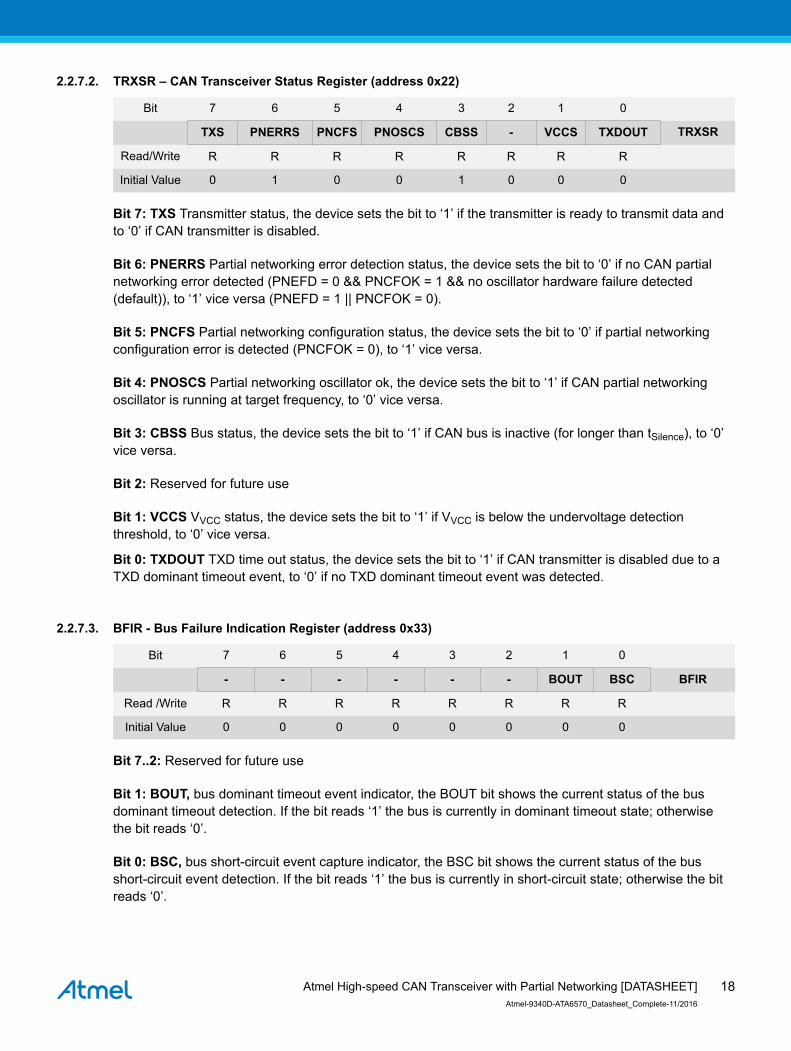
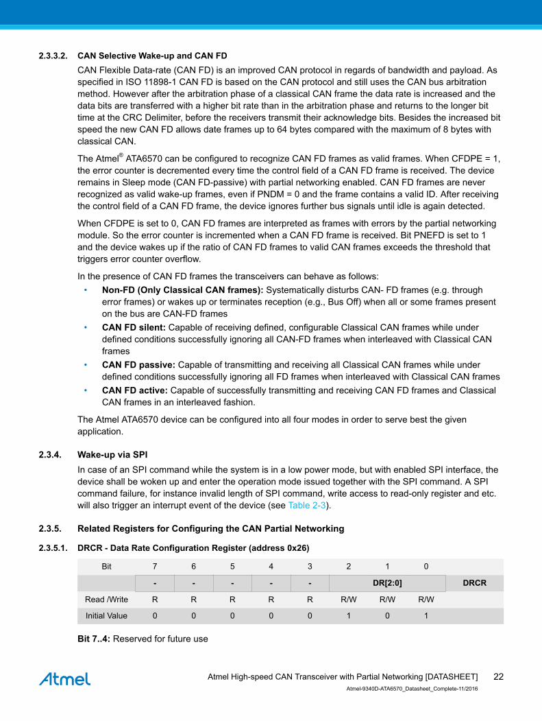
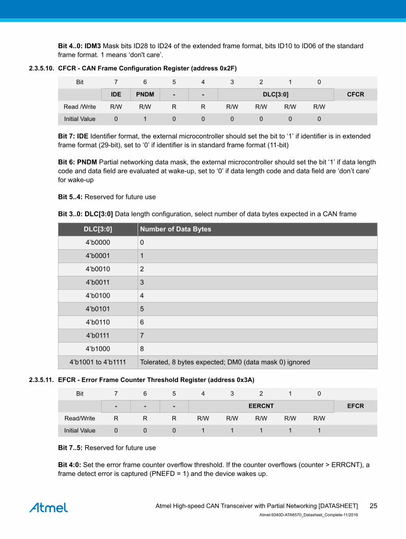
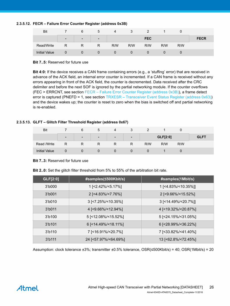
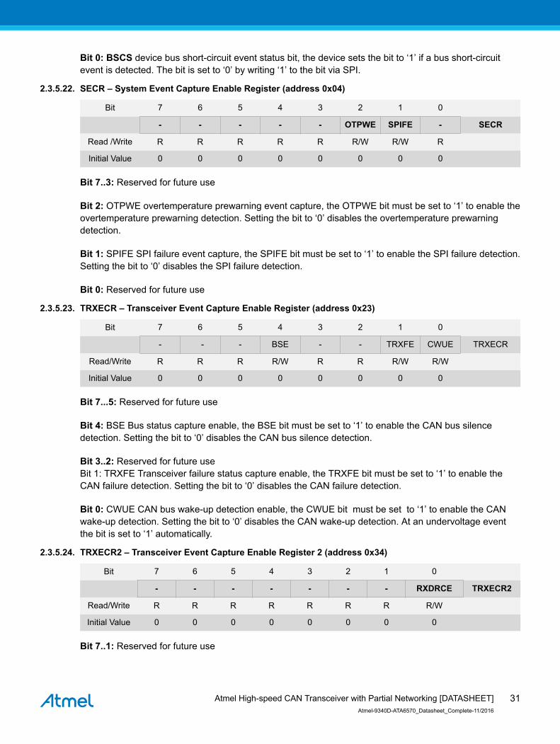
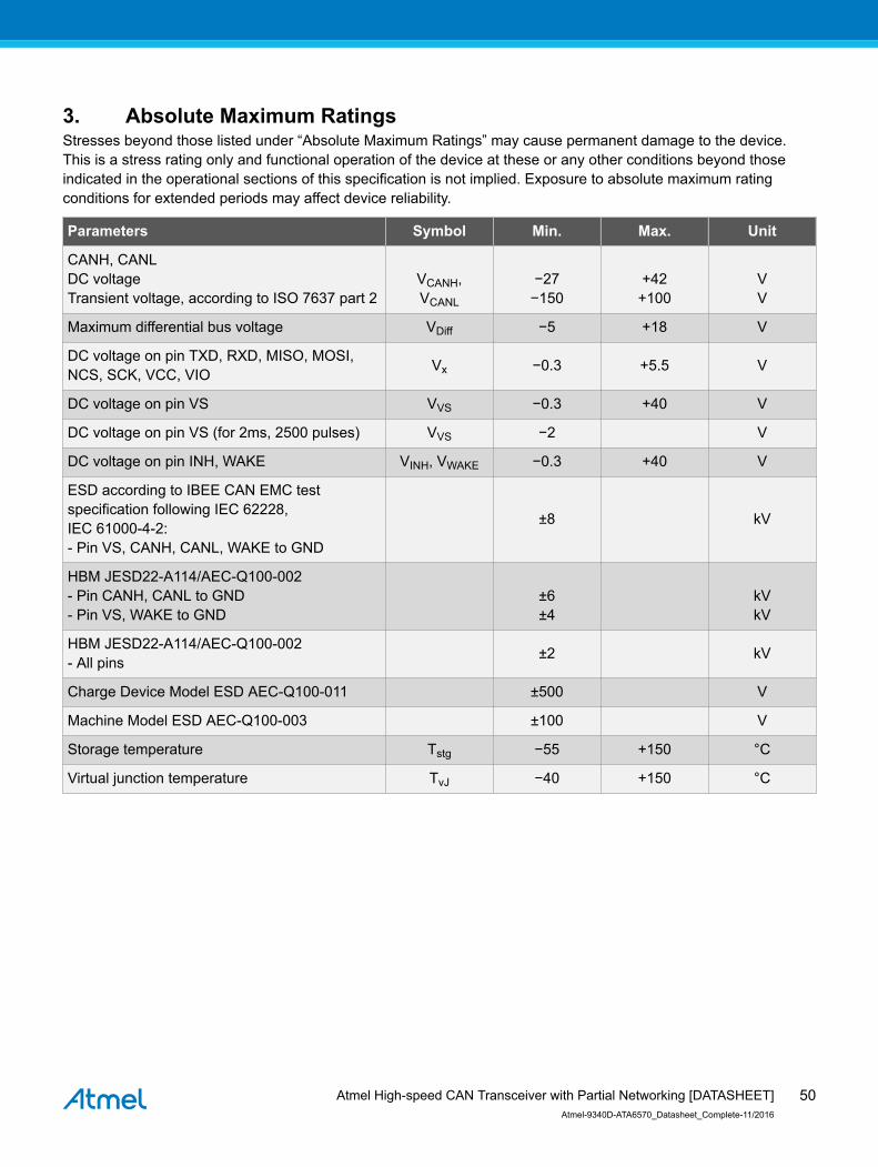

No Parameters Test Conditions Pin Symbol Min Typ Max Unit Type
9180 Delay time from bus wake-up to INHhigh Load on INH pin RLOAD = 10kΩ INH tWU_INH 100 micros A
9190 Undervoltage detection filter time VCCVIO tVSUP_UV_filter 6 54 micros A
9200Delay time from VIOVCCundervoltage detection to enterSleep mode
VCCVIO tUV2Sleep 200 400 ms B
9210 Startup time after power onFrom VVS rises above the power-ondetection threshold VVS_PWRONuntil pin INH high
VS tstartup 28 47 ms A
9220 Standard remote wake-up timeouttime
Between first and second dominantpulses CAN TRX Standby mode tWake 900 1200 micros B
9230 Debouncing time for recessiveclamping state detection
V(CAN_H-CAN_L) gt 900mVRXD = high RXD tRXD_rec_clmp 60 90 175 ns D
9240 Local wake-up time WAKE tlocal_wu 5 50 micros B
9250 Transmitter resume timeFrom TXD goes high to TX operatesafter TXD dominant timeout eventdetected
tTX_resume_TXDOUT
4 micros D
9260 Bus recessive clamping detectiontime
Bus recessive clamping time afterTXD goes low tbus_rec_clamp 1 micros D
SPI Timing
1010 Clock cycle time NormalStandby Sleep mode SPI tclk 250 ns D
1020 SPI enable lead time NormalStandby Sleep mode SPI tEN_Lead 50 ns D
1030 SPI enable lag time NormalStandby Sleep mode SPI tEN_Lag 50 ns D
1040 Clock HIGH time NormalStandby Sleep mode SPI tClk_H 125 ns D
1050 Clock low time NormalStandby Sleep mode SPI tClk_L 125 ns D
1060 Data input set-up time NormalStandby Sleep mode SPI tSetup 50 ns D
1070 Data input hold time NormalStandby Sleep mode SPI tHold 50 ns D
1080 Data output valid time NormalStandby Sleep mode SPI tDout_v 65 ns D
1090 Chip select pulse width high NormalStandby Sleep modepin MISO CL = 20pF SPI tNCS_pw 250 ns D
Temperature Protection
1110 Overtemperature protectionshutdown threshold TOT_Sdwn 157 174 190 degC B
1120 Overtemperature protection releasethreshold TOT_Release 120 134 147 degC B
1130 Overtemperature protectionprewarning threshold TOT_Prew 120 134 147 degC B
Type means A = 100 tested B = 100 correlation tested C = Characterized on samples D = Design parameter
Atmel High-speed CAN Transceiver with Partial Networking [DATASHEET]Atmel-9340D-ATA6570_Datasheet_Complete-112016
56
Figure 5-1 CAN Transceiver Timing Diagram 1
TXD
CANH
HIGH
LOW
HIGH
recessive
LOW
dominant
09V
05V
CANL
RXD
VDiff
td(TXD-busdom) td(TXD-busrec)
td(busdom-RXD)
tPD(TXD-RXD) tPD(TXD-RXD)
td(busrec-RXD)
07VIO03VIO
Figure 5-2 CAN Transceiver Timing Diagram 2
70
30
30
70
500mV
900mV
5 x tBit(TXD) tBit(TXD)
tBit(Bus)
tBit(RXD)
TXD
RXD
VDiff
Atmel High-speed CAN Transceiver with Partial Networking [DATASHEET]Atmel-9340D-ATA6570_Datasheet_Complete-112016
57
6 Application CircuitsFigure 6-1 Typical Application Circuit ATA6570
AtmelATA6570Microcontroller
MOSI
MISO
TXD
RXD
GND
SCK
NCSIO
IO
IO
IO
VDD
GND
TXD
RXD
VS
VBAT
12V
5V
CANH
WAKE
WakeSwitch
10nF
+
100nF
22microF
47nF
10kΩ
60Ω
60Ω
10kΩ
100nF
100nF
+
The value of these capacitors depends on the used external voltage regulators
VIO INH VCC
14 10
9
13
CANL12
5 7
2
3
8
11
6
1
12V
33V
CANH
CANL4
+
Figure 6-2 ATA6570 Test Circuit
RL2
CANH
RL2 C1
C2 VDiff
CRXD
VCANH
CANL
CANH
ATA6570
TXD
RXD
GND
CANL
13
122
4
1
VCANL
Atmel High-speed CAN Transceiver with Partial Networking [DATASHEET]Atmel-9340D-ATA6570_Datasheet_Complete-112016
58
7 Ordering InformationExtended TypeNumber Package
DescriptionRemarks
ATA6570-GNQW1 SO14 CAN transceiver with partial networking and watchdog(default off) CAN FD capable
4k tapedand reeled
Atmel High-speed CAN Transceiver with Partial Networking [DATASHEET]Atmel-9340D-ATA6570_Datasheet_Complete-112016
59
8 Package InformationFigure 8-1 SO14 Package
Package Drawing Contactpackagedrawingsatmelcom
GPC DRAWING NO REV TITLE
6541-505301-4 2
120214
Package SO14150 mil
COMMON DIMENSIONS(Unit of Measure = mm)
MIN NOM MAXSymbol
Dimensions in mm
specificationsaccording to DINtechnical drawings
018 025010A1
865 875855D1)
Note1) Dimensions ldquoDrdquo and ldquoE1rdquo do not include Moldflash or protrusion(MAX 015mm per side)
600 620580E
084 127040L127 BSCe
390 400380E1)
022 025019c042 051033b138 150125A2
155 175135A
1 7
14 8
E
E1
L
c
D
b
e
A
A2A1
Atmel High-speed CAN Transceiver with Partial Networking [DATASHEET]Atmel-9340D-ATA6570_Datasheet_Complete-112016
60
9 Revision HistoryPlease note that the following page numbers referred to in this section refer to the specific revisionmentioned not to this document
Revision No History
9340D-1116bull Section 5 Electrical Characteristics No 880 Sub Test Condition on
page 54 added
Atmel High-speed CAN Transceiver with Partial Networking [DATASHEET]Atmel-9340D-ATA6570_Datasheet_Complete-112016
61
Atmel Corporation 1600 Technology Drive San Jose CA 95110 USA T (+1)(408) 4410311 F (+1)(408) 4364200 | wwwatmelcom
copy 2016 Atmel Corporation Rev Atmel-9340D-ATA6570_Datasheet_Complete-112016
Atmelreg Atmel logo and combinations thereof Enabling Unlimited Possibilitiesreg and others are registered trademarks or trademarks of Atmel Corporation in US andother countries Other terms and product names may be trademarks of others
DISCLAIMER The information in this document is provided in connection with Atmel products No license express or implied by estoppel or otherwise to anyintellectual property right is granted by this document or in connection with the sale of Atmel products EXCEPT AS SET FORTH IN THE ATMEL TERMS ANDCONDITIONS OF SALES LOCATED ON THE ATMEL WEBSITE ATMEL ASSUMES NO LIABILITY WHATSOEVER AND DISCLAIMS ANY EXPRESS IMPLIEDOR STATUTORY WARRANTY RELATING TO ITS PRODUCTS INCLUDING BUT NOT LIMITED TO THE IMPLIED WARRANTY OF MERCHANTABILITYFITNESS FOR A PARTICULAR PURPOSE OR NON-INFRINGEMENT IN NO EVENT SHALL ATMEL BE LIABLE FOR ANY DIRECT INDIRECTCONSEQUENTIAL PUNITIVE SPECIAL OR INCIDENTAL DAMAGES (INCLUDING WITHOUT LIMITATION DAMAGES FOR LOSS AND PROFITS BUSINESSINTERRUPTION OR LOSS OF INFORMATION) ARISING OUT OF THE USE OR INABILITY TO USE THIS DOCUMENT EVEN IF ATMEL HAS BEEN ADVISEDOF THE POSSIBILITY OF SUCH DAMAGES Atmel makes no representations or warranties with respect to the accuracy or completeness of the contents of thisdocument and reserves the right to make changes to specifications and products descriptions at any time without notice Atmel does not make any commitment toupdate the information contained herein Unless specifically provided otherwise Atmel products are not suitable for and shall not be used in automotiveapplications Atmel products are not intended authorized or warranted for use as components in applications intended to support or sustain life
SAFETY-CRITICAL MILITARY AND AUTOMOTIVE APPLICATIONS DISCLAIMER Atmel products are not designed for and will not be used in connection with anyapplications where the failure of such products would reasonably be expected to result in significant personal injury or death (ldquoSafety-Critical Applicationsrdquo) withoutan Atmel officers specific written consent Safety-Critical Applications include without limitation life support devices and systems equipment or systems for theoperation of nuclear facilities and weapons systems Atmel products are not designed nor intended for use in military or aerospace applications or environmentsunless specifically designated by Atmel as military-grade Atmel products are not designed nor intended for use in automotive applications unless specificallydesignated by Atmel as automotive-grade
- Features
- Description
- Table of Contents
- 1 Pin Configuration
-
- 11 Supply Pin (VS)
- 12 Ground Pin (GND)
- 13 Supply Pin (VCC)
- 14 Supply Pin (VIO)
- 15 Bus Pins (CANH AND CANL)
- 16 Input Pin (TXD)
- 17 Output Pin (RXD)
- 18 Inhibit Output Pin (INH)
- 19 Wake Input Pin (WAKE only ATA6570)
- 110 SPI Input Pin (MOSI)
- 111 SPI Output Pin (MISO)
- 112 SPI Clock Pin (SCK)
- 113 SPI Chip Select Pin (NCS)
-
- 2 Functional Description
-
- 21 Device Operation Modes
-
- 211 Power Off Mode
- 212 Standby Mode
- 213 Sleep Mode
- 214 Normal Mode
- 215 Overtemp Mode
- 216 Microcontroller Reset Mode
- 217 Related Registers
-
- 2171 DMCR ndash Device Mode Control Register (address 0x01)
- 2172 DMSR ndash Device Mode Status Register (address 0x03)
-
- 22 Integrated CAN Transceiver Operation Modes
-
- 221 TRX Off Mode
- 222 TRX Standby Mode
- 223 TRX Biased Standby Mode
- 224 TRX Silent Mode
- 225 TRX Normal Mode
- 226 TRX Reduced Normal Mode
- 227 Related Registers
-
- 2271 TRXCR ndash CAN Transceiver Control Register (address 0x20)
- 2272 TRXSR ndash CAN Transceiver Status Register (address 0x22)
- 2273 BFIR - Bus Failure Indication Register (address 0x33)
- 2274 TRXESR2 ndash Transceiver Event Status Register 2 (address 0x35)
-
- 23 Wake-up in ATA6570
-
- 231 Local Wake-up via Pin WAKE
- 232 Remote Wake-up Pattern according to ISO 11898-5 (Partial Networking Disabled)
- 233 Remote Wake-up Frame according to ISO 11898-6
-
- 2331 CAN Selective Wake-up
- 2332 CAN Selective Wake-up and CAN FD
-
- 234 Wake-up via SPI
- 235 Related Registers for Configuring the CAN Partial Networking
-
- 2351 DRCR - Data Rate Configuration Register (address 0x26)
- 2352 CIDR0 - CAN ID Register 0 (address 0x27)
- 2353 CIDR1 - CAN ID Register 1 (address 0x28)
- 2354 CIDR 2 - CAN ID Register 2 (address 0x29)
- 2355 CIDR3 - CAN ID Register 3 (address 0x2A)
- 2356 CIDMR0 - CAN ID Mask Register 0 (address 0x2B)
- 2357 CIDMR1 - CAN ID Mask Register 1 (address 0x2C)
- 2358 CIDMR2 - CAN ID Mask Register 2 (address 0x2D)
- 2359 CIDMR3 - CAN ID Mask Register 3 (address 0x2E)
- 23510 CFCR - CAN Frame Configuration Register (address 0x2F)
- 23511 EFCR - Error Frame Counter Threshold Register (address 0x3A)
- 23512 FECR ndash Failure Error Counter Register (address 0x3B)
- 23513 GLFT ndash Glitch Filter Threshold Register (address 0x67)
- 23514 CDMR07 - CAN Data Mask Registers 07 (address 0x68hellip0x6F)
- 23515 BFECR - Bus Failure Event Capture Enable Register (address 0x32)
- 23516 PWKS ndash Pin WAKE Status Register (address 0x4B)
- 23517 GESR ndash Global Event Status Register (address 0x60)
- 23518 SESR ndash System Event Status Register (address 0x61)
- 23519 TRXESR ndash Transceiver Event Status Register (address 0x63)
- 23520 WKESR ndash WAKE Event Status Register (address 0x64)
- 23521 Bus Failure Event Indication Status Register (address 0x65)
- 23522 SECR ndash System Event Capture Enable Register (address 0x04)
- 23523 TRXECR ndash Transceiver Event Capture Enable Register (address 0x23)
- 23524 TRXECR2 ndash Transceiver Event Capture Enable Register 2 (address 0x34)
- 23525 WKECR ndash WAKE Event Capture Enable Register (address 0x4C)
- 23526 DIDR ndash Device ID Register (address 0x7E)
- 23527 RWPR ndash Register Write Protection Register (address 0x0A)
-
- 24 Fail-safe Features
-
- 241 TXD Dominant Timeout Function
- 242 TXD-to-RXD Short-circuit Detection
- 243 Bus Dominant Clamping Detection
- 244 Bus Recessive Clamping Detection
- 245 Internal Pull-up Structure at the TXD Input Pin
- 246 Undervoltage Detection on Pin VCC
- 247 Short-circuit Protection of the Bus Pins
- 248 RXD Recessive Clamping
- 249 Over-temperature Detection
- 2410 Loss of Power at Pin VS
- 2411 Wake-up and Interrupt Event Diagnosis via Pin RXD
- 2412 Interrupt EventWake-up Event Delay
- 2413 Sleep Mode Protection
-
- 25 WUP Detection and Bias Control
- 26 Device ID
- 27 Lock Control Register
- 28 Window Watchdog
-
- 281 WDTRIG - Watchdog Trigger Register (address 0x39)
- 282 Watchdog Behavior in Window Mode
- 283 Watchdog Behavior in Timeout Mode
- 284 Watchdog Behavior during Power-on and after Microcontroller Reset
- 285 Watchdog During VIO Undervoltage and Overtemperature
-
- 29 General-purpose Memory (GPMn)
-
- 291 General Purpose Memory 0 (address 0x06)
- 292 General Purpose Memory 1 (address 0x07)
- 293 General Purpose Memory 2 (address 0x08)
- 294 General Purpose Memory 3 (address 0x09)
-
- 210 VIO Supply Pin
- 211 VCCVIO Undervoltage Protection
- 212 Serial Peripheral Interface (SPI)
-
- 2121 General
- 2122 Register Summary
- 2123 Operating Modes and Register Bit Settings
-
- 3 Absolute Maximum Ratings
- 4 Thermal Characteristics
- 5 Electrical Characteristics
- 6 Application Circuits
- 7 Ordering Information
- 8 Package Information
- 9 Revision History
-
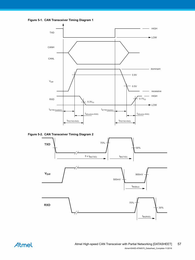
Related Documents