Idongesit Ebong (1-1) Jenna Fu (1-2) Bowei Gai (1-3) Syed Hussain (1-4) Jonathan Lee (1-5) Design Manager: Myron Kwai Overall Project Objective: Design a chip as part of a system that accommodates the growing demand for radio frequency identification (RFID) technology while creating a quicker, more convenient shopping experience. Presentation #9: Smart Cart 525 Stage IX: 16 Mar. 2005 Chip Level Layout

Overall Project Objective:
Dec 30, 2015
Presentation #9: Smart Cart 525. Idongesit Ebong (1-1) Jenna Fu (1-2) Bowei Gai (1-3) Syed Hussain (1-4) Jonathan Lee (1-5) Design Manager : Myron Kwai. Overall Project Objective: - PowerPoint PPT Presentation
Welcome message from author
This document is posted to help you gain knowledge. Please leave a comment to let me know what you think about it! Share it to your friends and learn new things together.
Transcript

Idongesit Ebong (1-1)Jenna Fu (1-2)
Bowei Gai (1-3)Syed Hussain (1-4)Jonathan Lee (1-5)
Design Manager: Myron Kwai
Overall Project Objective:Design a chip as part of a system that accommodates the growing demand for radio frequency identification (RFID)
technology while creating a quicker, more convenient shopping experience.
Presentation #9:
Smart Cart 525
Stage IX: 16 Mar. 2005Chip Level Layout
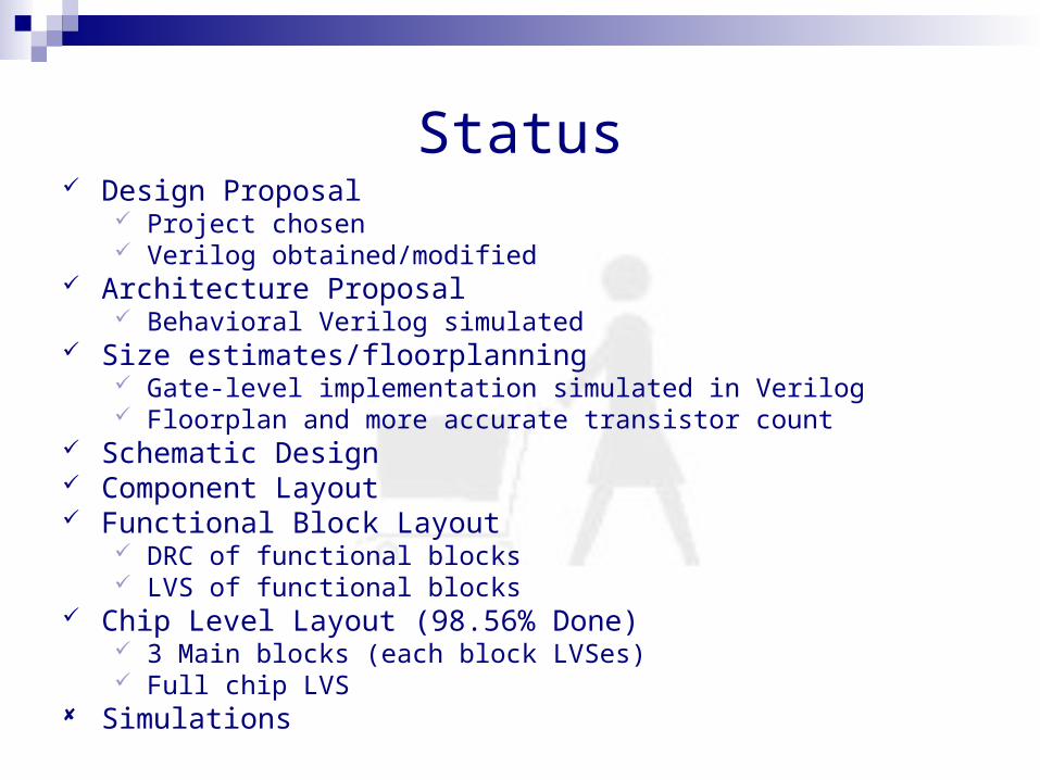
Status Design Proposal
Project chosen Verilog obtained/modified
Architecture Proposal Behavioral Verilog simulated
Size estimates/floorplanning Gate-level implementation simulated in Verilog Floorplan and more accurate transistor count
Schematic Design Component Layout Functional Block Layout
DRC of functional blocks LVS of functional blocks
Chip Level Layout (98.56% Done) 3 Main blocks (each block LVSes) Full chip LVS
Simulations

Design Decisions
Decided to route more wires over the SBOX and use metal 4 to reach registers on the right
Move items in the encryption block higher up and redesign SBOX logic

Previously…
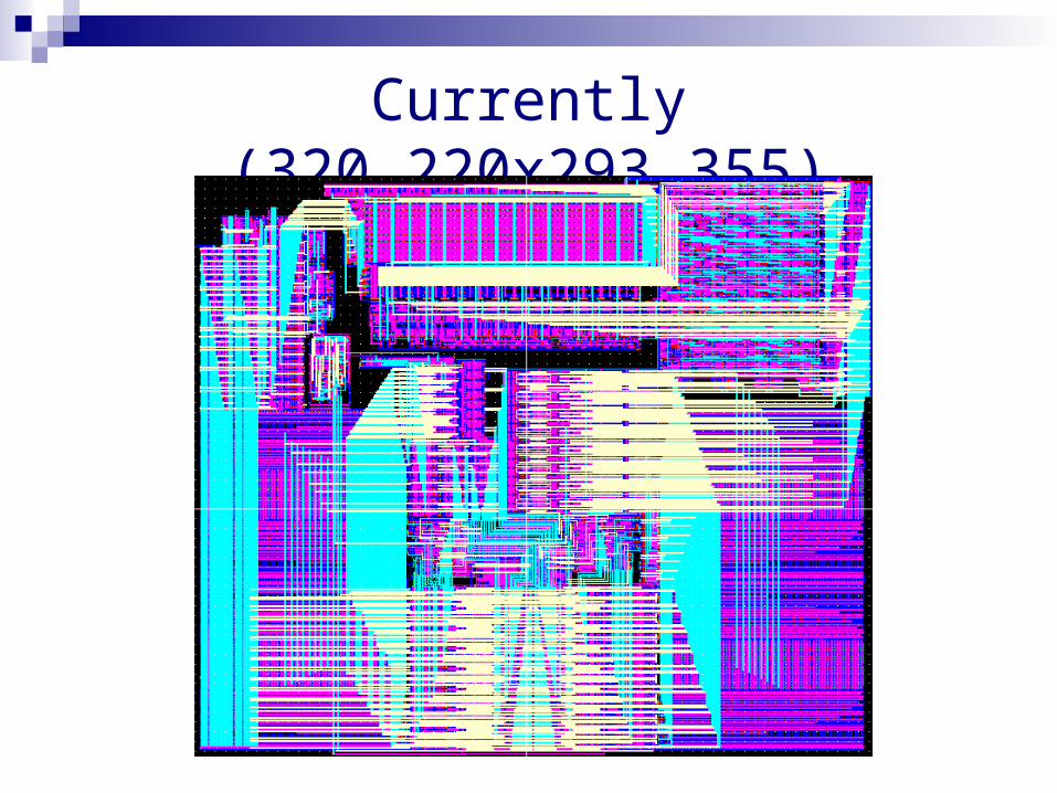
Currently (320.220x293.355)
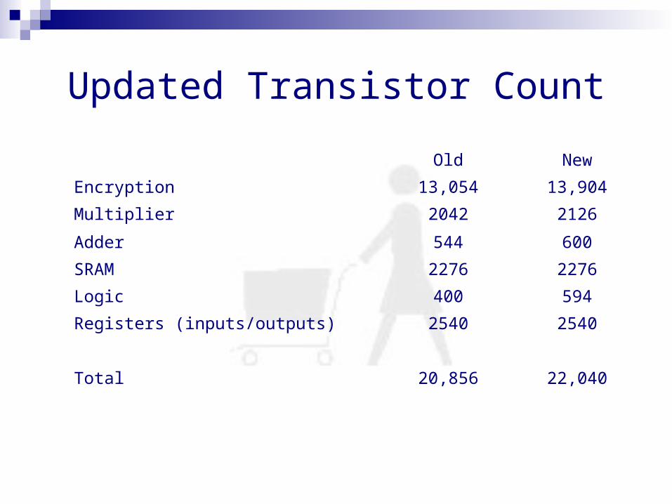
Updated Transistor Count
Old New
Encryption 13,054 13,904
Multiplier 2042 2126
Adder 544 600
SRAM 2276 2276
Logic 400 594
Registers (inputs/outputs) 2540 2540
Total 20,856 22,040

Updated Floorplan
Area: Old (μm2) New (μm2)
Encryption 68,352 60,983
Multiplier 8856 8420
Adder 3920 3429
SRAM 10,695 8183
Logic/Wiring 14,655 14,655
Registers (inputs/outputs, counters)
4490 4266
Total 110,968 91,365
Density: (transistors/μm2)
Aspect ratio:.191.36
0.261.1

Layer MasksPoly

Layer MasksMetal1

Layer MasksMetal2

Layer MasksMetal3
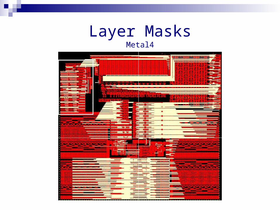
Layer MasksMetal4

Layout: Multiplier
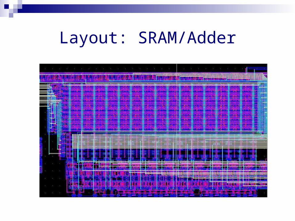
Layout: SRAM/Adder

Layout: FinalText/Initial Permutation

Layout: Mix Column/Rcon

Layout: Key Expand

Layout: SBOX

Problems & Questions
Registers problematic How can we make the chip smaller? Re-doing many of the blocks, learn from previous
mistakes. Reset signal strength and buffer size needed for
it. White space reduction Simulations take a long time.
Related Documents