Organic MEMS/NEMS-based high-efficiency 3D ITO-less flexible photovoltaic cells This article has been downloaded from IOPscience. Please scroll down to see the full text article. 2012 J. Micromech. Microeng. 22 115015 (http://iopscience.iop.org/0960-1317/22/11/115015) Download details: IP Address: 193.136.238.44 The article was downloaded on 29/09/2012 at 10:06 Please note that terms and conditions apply. View the table of contents for this issue, or go to the journal homepage for more Home Search Collections Journals About Contact us My IOPscience

Welcome message from author
This document is posted to help you gain knowledge. Please leave a comment to let me know what you think about it! Share it to your friends and learn new things together.
Transcript

Organic MEMS/NEMS-based high-efficiency 3D ITO-less flexible photovoltaic cells
This article has been downloaded from IOPscience. Please scroll down to see the full text article.
2012 J. Micromech. Microeng. 22 115015
(http://iopscience.iop.org/0960-1317/22/11/115015)
Download details:
IP Address: 193.136.238.44
The article was downloaded on 29/09/2012 at 10:06
Please note that terms and conditions apply.
View the table of contents for this issue, or go to the journal homepage for more
Home Search Collections Journals About Contact us My IOPscience

IOP PUBLISHING JOURNAL OF MICROMECHANICS AND MICROENGINEERING
J. Micromech. Microeng. 22 (2012) 115015 (11pp) doi:10.1088/0960-1317/22/11/115015
Organic MEMS/NEMS-basedhigh-efficiency 3D ITO-less flexiblephotovoltaic cellsSam Kassegne1,4, Kee Moon1, Pablo Martın-Ramos1,2,Mohammad Majzoub1, Gunay Ozturk1, Krishna Desai1, Mihir Parikh1,Bao Nguyen1, Ajit Khosla3 and Pedro Chamorro-Posada2
1 MEMS Research Lab, Mechanical Engineering Department, San Diego State University,5500 Campanile Drive, San Diego, CA 92182, USA2 Depto. de Teorıa de la Senal y Comunicaciones e Ingenierıa Telematica, Universidad de Valladolid,ETSI Telecomunicacion, Campus Miguel Delibes s/n, E-47011 Valladolid, Spain3 School of Engineering Science, Simon Fraser University, Burnaby, BC, V5A 1S6, Canada
E-mail: [email protected]
Received 26 June 2012, in final form 15 August 2012Published 26 September 2012Online at stacks.iop.org/JMM/22/115015
AbstractA novel approach based on three-dimensional (3D) architecture for polymeric photovoltaiccells made up of an array of sub-micron and nano-pillars which not only increase the area ofthe light absorbing surface, but also improve the carrier collection efficiency ofbulk-heterojunction organic solar cells is presented. The approach also introduces coating of3D anodes with a new solution-processable highly conductive transparent polymer (Orgacon
TM)
that replaces expensive vacuum-deposited ITO (indium tin oxide) as well as the additionalhole-collecting layer of conventional PEDOT:PSS (poly(3,4-ethylenedioxythiophene)poly(styrenesulfonate)). In addition, the described procedure is well suited to roll-to-rollhigh-throughput manufacturing. The high aspect-ratio 3D pillars which form the basis for thisnew architecture are patterned through micro-electromechanical-system- andnano-electromechanical-system-based processes. For the particular case of P3HT(poly(3-hexylthiophene)) and PCBM (phenyl-C61-butyric acid methyl ester) active material,efficiencies in excess of 6% have been achieved for these photovoltaic cells of 3D architectureusing ITO-less flexible PET (polyethylene terephthalate) substrates. This increase in efficiencyturns out to be more than twice higher than those achieved for their 2D counterparts.
(Some figures may appear in colour only in the online journal)
1. Introduction
In recent years, there has been a significant increase in interestin various forms of renewable energy sources, which areseen as the key to long-term weaning from strict relianceon fossil fuels such as oil, coal and natural gas [1]. Amongthese, solar energy conversion is perhaps the most appealingsince the energy source is readily available and practicallyinexhaustible.
4 Author to whom any correspondence should be addressed.
To date, silicon photovoltaic (PV) cells with an efficiencyof about 25% have been demonstrated [2]. Unfortunately,such high efficiency bulk-silicon PV cells are prohibitivelyexpensive for mass production. As a result, most of today’scommercial-grade silicon PV cells packaged in modules areless than 20% efficient with typical efficiencies of only≈14–17% [3].
In the meantime, the multi-billion dollar PV industrycontinues to grow at a remarkably high rate. Therefore, findinginnovative approaches for a single device technology that arecompetitive in efficiency and cost with other energy sourcesfor both secondary and primary power generation continues
0960-1317/12/115015+11$33.00 1 © 2012 IOP Publishing Ltd Printed in the UK & the USA
J. Micromech. Microeng. 22 (2012) 115015 S Kassegne et al
to be of great interest and unmet need for the PV researchand industrial communities. As a background to the approachpresented here, we briefly review recent works in improvingefficiencies of PV cells.
A number of concepts for increasing the efficiency of PVcells above the single-junction limit continue to be proposed[4]. These new generations of PV cells are based on severalnew band structure and energy conversion concepts that havethe potential to achieve limiting efficiencies greater than thesingle-junction limit. It is expected that such technologies,which are still emerging, will also be able to achieve costlevels similar to or better than previous generation of PV celltechnologies.
One such example is the multi-junction cell (MJC) whichallows the absorption of a wider range of wavelengths in thesolar spectrum by combining PV cells of varying bandgap in aseries (tandem) stack [5]. At present, however, these cells areexpensive and their use is limited to space applications as wellas terrestrial concentrator systems in solar power stations inwhich a small area is necessary.
Another leading concept for high efficiency is theintermediate band (IB) PV cell [6, 7]. Again, the idea isto absorb more of the solar spectrum by introducing stateswithin the bandgap of a semiconductor material such that low-energy photons can be absorbed in a two-photon process thatpromotes charge carriers to the conduction band. Such a bandstructure would have a theoretical limiting efficiency of ≈60%and thus has great promise [8]. However, to date very few bulkmaterials have been shown to possess such intermediate states.At present, IB PV cell concepts are in the early research stage,although they continue to be of great interest for future PVdevice applications.
A third approach for high efficiency PV cells is theconcept of carrier multiplication where for a single absorbedphoton, more than one electron–hole pair is generated, mainlyby an avalanche-type process employing a high local field[9, 10]. However, the practical aspects of this, including chargeseparation, etc require additional basic research. Further, thereare various efforts in up- or down-conversion of photonsinto a suitable energy regime for a single bandgap PV cell[11]. This is primarily done by the use of an additional layerintegrated above or behind the cell. The layer typically consistsof micron- or nano-sized phosphor particles that absorb partof the spectrum and convert it to more suitable energy for thePV cell in the composite system. To date, efforts in down-conversion have been successful using bulk materials andwith limited success when using nano-structures [12]. Whileresearch continues in developing such ultra-high efficiencyPV cells, there are also significant efforts to develop thin-film single-junction PV cells in order to decrease the cost asreported in a review by Chopra et al [13].
On the other hand, bulk-heterojunction PV cells holdsignificant promise for the future. While conventionalP3HT:PCBM-based bulk-heterojunction PV cells (excludingtandem approaches) have seldom achieved conversionefficiencies in excess of 4–4.5% [14], the introduction oflow-bandgap polymers such as PCPDTBT (poly[2,6-(4,4-bis-(2-ethylhexyl)-4H-cyclopenta[2,1-b;3,4-b′]dithiophene)-alt-4,7-(2,1,3-benzothiadiazole)]) with absorption up to 900 nm
has pushed conversion efficiencies to 5.5% [15] and in a recentcase to 6.1% [16]. A review by Li et al [17] documents recentprogress in conversion efficiencies to the 7–8% range throughother high-performance low-bandgap polymers composed ofthieno[3,4-b]-thiophene (TT) and benzodithiophene (BDT)alternating units.
In addition to advances in photoactive materialdevelopment, an increasing amount of recent work in organicPV cells has concentrated on exploring approaches involvingnewer architectures—particularly architectures that exploit thethickness dimension resulting in 3D configurations [18–26].Coupled with improvements in the chemistry and physics ofphotoactive layers and advances in electrode materials withfavorable bandgap properties, these improvements in overalldevice design and architecture are hoped to enable furtherincreases in conversion efficiencies. In their basic form, mostof these new 3D architectures typically involve sub-micronand—increasingly—nano-structures as part of the electrodematerial or part of the light conversion layer or in some casesboth [19].
In general, these 3D nano-structures applied to PV cellsare usually classified into four types: (a) nanocompositesand nano-structured polycrystalline materials, (b) quantumwells, (c) nano-pillars/nano-wires and (d) nanoparticles andquantum dots. These structures have been employed in variousfunctions and for various performance/energy-conversionenhancement strategies. The review paper by Tsakalakos[20] discusses the major synthetic methods for each of theaforementioned nano-structure classes along with a discussionon the potential advantages and disadvantages of each nano-structure approach. The paper also provides a critical reviewof the major works that have utilized the particular nano-structure type in a PV cell along with works where fundamentalmeasurements of key parameters of interest to PV have beenperformed.
A further review of some of the recent notable works in3D nano-structures is given here. Aryal et al fabricated large-scale high density polymer nanopillars using nanoimprintinglithography for bulk-heterojunction PV cells [21, 22]. Theyproduced nanoporous silicon molds through inductivelycoupled plasma etching which were then used to nano-imprintordered and dense polymer nano-pillars and nanopores inSU-8, PMMA (poly(methyl methacrylate)), P3HT and PCBM.Subsequently, the imprinted P3HT nano-pillars were used tomake bulk-heterojunction PV cells by depositing PCBM ontop of the pillars, proving that the interdigitized heterojunctionmorphology leads to improved PV cell performance. Tsai etal used Au nanopillars and showed higher external quantumefficiency in a narrow wavelength range (∼640–720 nm) wherethe active layer (P3HT:PCBM) absorption is relatively low[23]. Randomly oriented nanorod electrodes (100–150 nmheight and 15–30 nm thickness) deposited on an ITO-coatedglass substrate using an oblique electron-beam evaporationmethod were reported by Yu and colleagues [24] with anincrease in PCE (power conversion efficiency) of 3.4%. Zhouet al used P3HT nanogratings shaped by nanoimprintinglithography to enhance hole mobility and induce a stronganisotropy of conductance due to 3D polymer chain alignment
2

J. Micromech. Microeng. 22 (2012) 115015 S Kassegne et al
Figure 1. Architecture of a 3D organic PV cell. Flexible and transparent substrate (PET) is used, on top of which 3D pillars are fabricatedusing SU-8
R©. On top of these pillars, a metal cathode layer is deposited followed by a thin layer of photoactive material. The final layer
consists of transparent conductive polymer.
[25]. Their reported improvement in PCE from 2.5% to2.76% was driven by improved short-circuit current, Isc. Riderand colleagues reported ITO and hybrid ITO/SiO2 nano-pillars fabricated via glancing angle deposition (GLAD) thatfunction as 3D high surface-area transparent electrodes [26].After adding insulating SiO2 caps above the GLAD ITOnano-pillars to produce a hybrid ITO/SiO2 nanoelectrode,PCE of 2.5% was achieved as a consequence of reducedelectrical shorting and series resistance. Chen and colleaguesreported a hybrid solar cell using electrochemically preparedmetallic carbon nanotube (CNT)–polythiophene (PT) core-shell nanowire networks, with PCBM added in the openings[27]. They demonstrated a PCE of 2.76% at 100 mW cm−2, 1sun (and 3.07% at 1000 mW cm−2, 10 suns).
As these recent works discussed above suggest, we believethat new innovations in PV (particularly organic PV) willcontinue to be driven by architecture-specific advances suchas 3D electrode and light trapping mechanisms as well asinnovative and economical manufacturing techniques thatscale very well. Addressing these research needs serves asthe motivation for this current research.
2. A novel alternative approach: SU-8 pillars-based3D flexible PV cells
In this study, we present the investigation of improvedefficiencies for organic bulk-heterojunction PV cells through3D architecture coupled with anodes coated with a newsolution-processable highly conductive transparent polymer.The particular case of P3HT:PCBM active polymer-basedbulk heterojunction is considered here, even though the sameapproach works for newer high-performance polymers withlow bandgap. Our approach involves the introduction of(i) high aspect-ratio micro- and nano-3D pillar electrodesthat can be manufactured using lithography processescommon for MEMS/NEMS (micro-electromechanical andnano-electromechanical systems), (ii) new optimized and
economical process using conductive polymer that replacesexpensive transparent metal oxides such as ITO (indiumtin oxide) as well as the additional hole-collecting layer ofconventional PEDOT:PSS and (iii) flexible and transparentsubstrates amenable to roll-to-roll (R2R) high-throughputmanufacturing platform. Taken together, we submit that thesethree approaches will offer a significant improvement in theconversion efficiency as well as economics of these almostall-organic bulk-heterojunction PV cells.
2.1. 3D micro- and nano-architecture
The main concept behind 3D electrode architecture PV cellpresented here is the collection of energy not just from twoplanar electrodes, but also from numerous cylinder shaped highaspect-ratio micro- and nano-electrodes as shown in figure 1.The 3D concept presented here consists of a polymer precursor(such as SU-8 R©) patterned into an array of pillars that act as astructural material which support the anode layer, photoactivelayer and cathode layer. Typically, a flexible and transparentsubstrate such as PET is used, on top of which 3D pillarsare fabricated using SU-8 R© which is a high contrast, epoxy-based negative-tone photoresist designed for micromachiningand other microelectronic applications. SU-8 R©which was alsoreported to offer some resistance to degradation due to UV light[28] is assayed as a tentative material for the pillars throughdirect photolithography or nanoimprinting [29]. As shown infigure 1, we introduce the use of a transparent conductivepolymer, namely, OrgaconTM (S305Plus R©) which is coated ontop of 3D pillars to form the anodic component. OrgaconTM isa commercial variety PEDOT:PSS with a work function of5.1 eV [30]. It has also been shown that Orgacon’s workfunction can be reduced to 4.8 eV by the addition of sorbitol[31]. A thin layer of photoactive material in the order of 100 nmand less is then applied through spin-coating. As a final layer,a metal cathode layer of 80–100 nm thickness is thermallyevaporated.
3

J. Micromech. Microeng. 22 (2012) 115015 S Kassegne et al
In general, the benefits of this 3D architecture over thetwo-dimensional (2D) cells include: an increase in the surfacearea, absorbance asymptote reaching to 100% due to reflectionbenefits and broader incident light angle range around highabsorption efficiencies [15–29]. The specific advantages ofPV cells based on 3D nano-pillar architecture are discussedbelow. These discussions are also relevant for 3D pillars in thesub-micron range as well.
(i) Increased optical thickness. The 3D geometry ofthe electrodes enables increased optical thickness(hence access to more light energy) and decreaseddiffusion length for migrating charges [28]. Further,the 3D architecture introduced here supports multiplephotoactive layers of different types to absorb differentpeaks of spectrums within visible light. This, in turn,provides enhanced absorption of photonic energy andhence increased efficiency.
(ii) Reduced optical reflection and enhanced absorption.Nano-pillar arrays provide a unique advantage due totheir anti-reflective and light trapping properties. Nano-pillar-arrays-based PV cells of only several microns inlength have been noted for their strong broadband opticalabsorption and dark visual appearance [32, 33]. Numericalstudies on the optical properties of disordered nano-pillararrays by diffuse scattering [34] and ordered verticalarrays by specular reflection [35] have demonstratedthat nano-pillar arrays have distinct absorption spectracompared to their thin-film counterparts. The orderingof the arrays may be used as light trapping schemesanalogous to random surface texturization or periodicgrating couplers in thin films [36]. Nano-pillar arrayscan be used to redistribute the absorption spectrum fromregions where absorption is not needed to spectral regionswhere absorption enhancement would lead to enhancedphotocurrents. The array material, diameter, length andpitch can all be optimized to tailor the absorption spectrumof the nano-pillar PV cell. Additional parameters suchas tapering of the pillars or pillars of different diametersmay further improve upon the anti-reflective and enhancedabsorption properties [35].
(iii) Enhanced carrier collection efficiency. Nano-pillar-basedPV cells introduce important changes in the dynamicsof carrier collection efficiency as compared to their thin-film counterparts. Among other factors, high efficiencyin traditional thin-film PV cells requires efficient lightabsorption and carrier collection [37]. Yet, absorption andcollection are in competition in thin-film devices [38, 39].Nano-pillar PV cell architectures offer the advantage oforthogonalizing these two processes, thereby relieving thecompetition between them and opening the design spacefor further optimization [38]. In short, device thicknesscan be designed to account for the absorption lengthof the material, while the nano-pillar radial junctionscan be optimized for minority diffusion lengths in thesurrounding medium.
2.2. Conductive transparent polymer anode
Further, the proposed device architecture diverges from thetraditional 2D polymer PV cell [40] not only on the 3Danode structure based on polymer precursors, but also onthe fact that traditional ITO sputtering deposition is nolonger used. This expensive component of the manufacturingprocedure for ITO is replaced by the deposition of a solution-processable, highly conductive transparent polymer calledOrgacon (S305Plus R©), achieving conformal deposition onthe pillars both on rigid and flexible substrates. As it turnsout, the use of this single conductive polymer as an anodematerial also enables a significant advantage of economical,automated R2R high-throughput manufacturing by removingthe expensive vacuum deposition process. To the best of theauthors’ knowledge, this is the first time a deposition of atransparent and conductive polymer such as OrgaconTM isreported on 3D anodic structures with varying aspect ratio andspacings supported on a flexible substrate.
Arrays of electrode pillars with sub-micron and nanometerrange diameter are fabricated. We have investigated a widerange of geometry of the pillar arrays varying from 20 μmdiameter at 20 μm spacing and height of 30 μm down to750 nm diameter at 750 nm spacing. For larger spacings anddiameters in the range of 1 μm and above, direct negativelithography of SU-8 is used. For tighter spacings and diametersin the sub-micron and nanometer ranges, nanoimprinting isused [26]. Nanoimprinting lithography for bulk-heterojunctionPV cells has also been used by several groups such as Aryalet al who have imprinted large-scale high density polymernanopillars for organic PV cells [21, 22].
2.3. Flexible PET substrate
Manufacturing processes well-suited to R2R high-throughputmanufacturing offer an added advantage in commercialcompetitiveness of organic PV cells. We investigate the useof PET (polyethylene terephthalate) which provides highflexibility, transparency, high melting point and compatibilityto lithographic processes as a flexible substrate platform.Further, this organic substrate offers an almost ‘all-organic’PV platform.
In general, the use of high aspect-ratio 3D pillarsmanufactured from a polymer precursor (such as anegative-tone photoresist) and coated with a highlyconductive transparent polymer (as opposed to conventionalconductive metal oxides) that is well-suited to scalableand high-throughput R2R manufacturing process are uniquecontributions of this research.
3. Materials and methods
3.1. Manufacturing procedures
We prepared several 3D PV chips using both PET and glasssubstrates. Typical overall chip sizes are 1.5 cm × 1.5 cm.As experimental control, we also manufactured and tested2D chips on ITO-coated substrates. ITO-coated glass slidespurchased from Delta Technologies (Stillwater, MN) were
4
J. Micromech. Microeng. 22 (2012) 115015 S Kassegne et al
used as a rigid substrate platform and offer experimentalcontrols. PET purchased from McMaster-Carr (Los Angeles,CA) was used for the flexible prototypes.
The 3D nano-pillar array on the anode side was formedeither through nanoimprinting or negative photolithographyprocess (for features larger than 1–2 μm). Nanoimprintingprocess as described in [29] is used to make the nano-pillararray with typical dimensions of 750 nm diameter, 750 nmheight and 750 nm spacing. The alternative manufacturingprocess for larger features in the range of 2 μm andabove involves lithography process using SU-8TM (fromMicrochem R©). The lithography consists of the usual steps5
(with slight variations for the various grades for the negative-tone photoresist): (i) substrate pretreatment; (ii) photoresistcoating by spin-coating at 2000 rpm for 45 s; (iii) soft bakingfor 20 min, starting at 65 ◦C and increasing 5 ◦C every 5 minup to 100 ◦C; (iv) UV light exposure (6 mW cm−2 for 40 s);(v) post-exposure baking for 15 min, starting at 65 ◦C for thefirst 5 min and then increasing to 100 ◦C for the remaining10 min; (vi) developing for 5 min and (vii) hard baking for30 min at 120 ◦C to enhance the strength of the fabricatedstructure. These processes are slightly modified for differentSU-8 grades such as SU8–2, SU8–10 and SU8–100 as well asfor chips of varying spacings and heights.
Once the 3D substrate was prepared, three layers ofS305Plus R© (one of the novel OrgaconTM formulations) areapplied to form the anodic component. S305Plus R© is highlytransparent conductive polymer and was purchased fromAgfa Materials (Mortsel, Belgium). S305Plus R© is compatiblewith almost all types of substrates. The S305Plus R© wasdeposited by spin-coating at 350 rpm for 45 s with bakingcycles in-between depositions to remove solvent (3 min at120 ◦C). The resistance of such layer is then measuredand confirmed not to exceed 150–200 �. This was thenfollowed by a conformal deposition of photoactive materialconsisting of a blend of PCBM (phenyl-C61-butyric acidmethyl ester) and P3HT (poly(3-hexylthiophene)). PCBMwas purchased from nano-C (Westwood, MA) and was usedwithout further purification. P3HT was purchased from RieksMetal Inc. (Lincoln, NE). The solvent dichlorobenzene (DCB)was bought from Sigma-Aldrich (St. Louis, MO). A blendof P3HT/PCBM in 1:1 wt/wt ratio was prepared by firstdissolving P3HT in 1,2- DCB to make a 17 mg ml−1 solution,followed by blending with PCBM in 50 wt%. The blend wasthen stirred overnight, filtered and then spin-coated at 350 rpmfor 45 s. The wet photoactive film was allowed to solidify for90–120 min in a closed container and then annealed overnightin N2 environment at 85 ◦C to improve the degree of self-organization.
The aluminum cathode layer was then thermallyevaporated in an atmosphere of 1 × 10⁻⁶ Torr on top of theorganic layer. The final thickness of the aluminum layer was80–100 nm as measured by the Alpha Step 200 profilometer(Tenkor Instruments). Finally, wire-bonding was done by firstheating the devices at 100 ◦C for 10 min and then using ablend of silver-epoxy and epoxy-hardener in the ratio of 1:1.
5 Microchem. Nano TM SU-8 Negative Tone Photoresist Formulations 50–100 Datasheet.
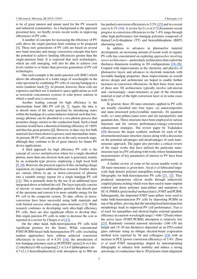
Figure 2. Example of a 3D flexible substrate: pillars on PET slide.No deposition of cathode, photoactive material and anodic layer isdone yet.
The complete optimized fabrication processes are summarizedin table 1.
3.2. Manufacturing conditions
The light conversion efficiency of the cells is stronglydependent on the manufacturing processes. Some of the keyparameters of manufacturing that require process optimizationinclude
(i) Uniform deposition of metal on the sides as well as top ofmicro- and nano-pillars. This is achieved by continuouslyrotating the dies at a diagonally positioned platform whilemaintaining 1 × 10⁻⁶ Torr vacuum for 60 s. The sampleis kept in a vacuum chamber for 20 min.
(ii) The conformal deposition of a thin film of photoactivelayers (P3HT and PCBM). After deposition, the layer isallowed to dry in air. If non-uniformity exists, additionallayers of photoactive materials should be deposited andthen air-dried. This requires annealing in N2 environmentat 85 ◦C to improve self-organization.
(iii) A thin and uniform layer of S305Plus R©which is depositedby spin-coating at 350 rpm for 45 s, with baking cyclesin-between depositions to remove solvent. As many asthree layers are needed for this.
(iv) For tighter spacings of the pillars in sub-micron andnanometer range, it was noted that high vacuum in therange of 1 × 10⁻⁶ Torr is required to thermally evaporatea smooth conformal deposit of aluminum. In typical cases,not applying enough vacuum in this range was observed toresult in the metal layer forming a bridge between adjacentpillars instead of a smooth conformal deposit.
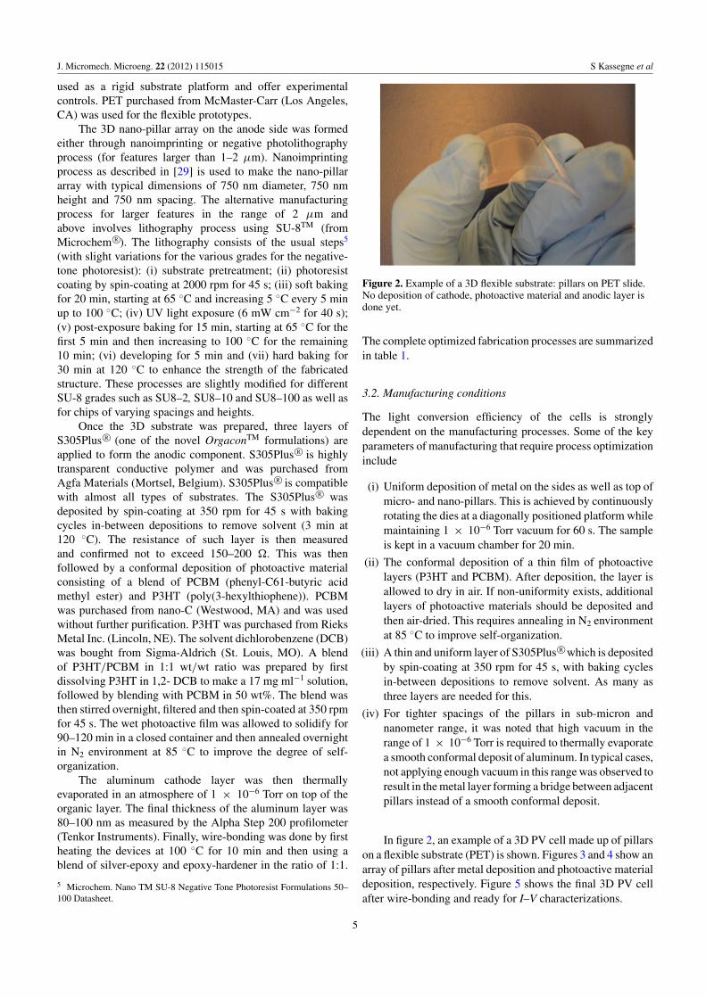
In figure 2, an example of a 3D PV cell made up of pillarson a flexible substrate (PET) is shown. Figures 3 and 4 show anarray of pillars after metal deposition and photoactive materialdeposition, respectively. Figure 5 shows the final 3D PV cellafter wire-bonding and ready for I–V characterizations.
5
J. Micromech. Microeng. 22 (2012) 115015 S Kassegne et al
Figure 3. Detail of pillars before deposition of metal and P3HT/PCBM. Sizes are 10 μm and 2 μm � with 10 μm and 2 μm spacings,respectively.
Table 1. Summary of the lithography process for fabrication of 1.5 cm × 1.5 cm PV chips (optimized for SU8–10).
Step Details Specifications
1. Negative photolithography1.1 Cut substrate PET 1.5 cm × 1.5 cm slide1.2 Clean substrate IPA, acetone twice1.3 Dehydration bake Hot plate 45 min, 50 ◦C1.4 Spin coat neg. photoresist SU-8 (10/100) 2000 to 3000 RPM, 45 s1.5 Soft bake Hot plate 65–100 ◦C, 5 ◦C intervals, 20 min1.6 Cool down Hot plate Gradually reduce temp, 15 min1.7 UV exposure UV lamp 6–8.5 mW cm−2, 20–40 s1.8 Post-exposure bake Hot plate 65–100 ◦C, 5 ◦C intervals, 75 min1.9 Cool down Hot plate Gradually reduce temp, 15 min1.10 Develop photoresist Developer 5 min, fume hood1.11 Rinse and dry IPA, air Blow-dry with N2 gun2. OrgaconTM deposition2.1 Tape slide∗ Teflon tape One edge of slide2.2 Spin coat first layer OrgaconTM 350 RPM, 45 s2.3 Anneal first layer Hot plate 120 ◦C, 3 min2.4 Spin coat second layer OrgaconTM 350 RPM, 45 s2.5 Anneal second layer Hot plate 120 ◦C, 3 min2.6 Spin coat third layer OrgaconTM 350 RPM, 45 s2.7 Anneal third layer Hot plate 120 ◦C, 3 min2.8 Check conductivity Multi-meter <200 Ohms3. P3HT:PCBM deposition3.1 Spin coat P3HT:PCBM 350 RPM, 45 s3.2 Air dry Dark container 2 h3.3 Anneal N2 oven 12–24 h 85 ◦C4. Aluminum deposition4.1 Tape slide Teflon tape Remaining sides, and down the middle4.2 Thermal evaporation TE machine <40 A, 25–30 s4.3 Settle particles Vacuum chamber 10 min5. Remove tape Manual 1 min6. Wire–bonding6.1 Heat the chip Hot plate 100 ◦C for 10 min6.2 Wire bond Wire bonder Blend of silver-epoxy and epoxy-hardener in the ratio of 1:1.
3.3. Testing conditions
Testing was done under the standard simulated AM1.5Girradiation using an Oriel 91159 150 W Full SpectrumSolar Simulator with a 2′′ × 2′′ full spectrum collimatedoutput (1000 W m−2). The AM1.5 solar simulatorspectrum has been double-checked using a calibratedphotodiode at different wavelengths and compared to thestandard. Further, the intensity in suns was always double-
checked prior to the measurements using a calibrationcell.
For testing purposes, the PV cells were always placed in aperfectly horizontal position to eliminate any additional effectof directionality of light. As one of the distinguishing aspectsand unique advantages of PV cells based on 3D architecture isthe increase in the surface area exposed to light; it is expectedthat the solar conversion efficiency could further increasedepending on the orientation of the chip. Our preliminary
6

J. Micromech. Microeng. 22 (2012) 115015 S Kassegne et al
Figure 4. (a) Optical image of array of pillars (10 μm �, 25 μm spacing and 20 μm height) after deposition of metal (Images taken withHirox 3D microscope). (b) SEM image of the same chip after deposition of photoactive material and Orgacon layer.
Figure 5. Final wired flexible device ready for I-V characterization.
geometrical simulation models of a given size of the PVcell taking into account the azimuth and elevation of lightsource suggest that for optimized spacing, diameter and heightof pillars, the total illuminated area approaches a maximumvalue at an angle of elevation of 45◦ and finally reduces to aminimum at 90◦. This aspect is under further investigation andwill be reported in a separate paper. However, for comparisonpurposes and to provide a control experiment, all reportedresults here are based on PV cells exposed to light in theperpendicular direction.
The conversion efficiency (η) of solar cells is typicallyexpressed as follows:
η = FF × ISC × VOC/Pin, (1)
where FF, ISC, VOC and Pin are fill factor, short-circuit current,open-circuit voltage and the incident power, respectively.
4. Results and discussions
The summary of device architectures for the various PVdevices fabricated in this work is presented in table 2 andthe respective device performances are provided in table 3.
Table 2. Device architectures of the various organic PV cells in thiswork.
Device type Device architecture
2D ITO Glass pre-coated withITO/P3HT:PCBM/Al
3D ITO Glass pre-coated with ITO/SU-8Pillars/P3HT:PCBM/Al
2D PET Orgacon PET/OrgaconTM/P3HT:PCBM/Al3D Glass Orgacon Glass/SU-8
Pillars/OrgaconTM/P3HT:PCBM/Al3D PET Orgacon PET/SU-8
Pillars/OrgaconTM/P3HT:PCBM/Al
The series of devices which consists of a total five uniquetypes includes cells manufactured on top of commercial glassslides pre-coated with ITO (i.e. ‘2D ITO’ and ‘3D ITO’),2D PV cells fabricated using PET and OrgaconTM (i.e. 2DPET Orgacon) and two PV cells fabricated with the novelarchitecture introduced in this study (one fabricated on a rigidsubstrate (i.e. 3D Glass Orgacon) and the other on a flexiblePET substrate (i.e. 3D PET Orgacon)). The overall sizes of allthe cells are fixed at 1.5 cm × 1.5 cm. The active surface areawhich is covered by P3HT:PCBM is 1 cm × 1 cm giving a netphotoactive area of 1.0 cm2. Note that the anodic componentof the chip designated as ‘3D ITO’ is still 2D; it is only thecathodic component as well as the photoactive layer that isdeposited on the pillar structures.
The first three devices have been included for comparisonpurposes. The comparison proves to be reliable since the fivedevices have been manufactured consecutively in the samework session using the same starting materials and havingtheir cathodes evaporated simultaneously. Further, all the chipshave a net photoactive area of 1.0 cm2. Our first two devices(i.e. ‘2D ITO’ and ‘3D ITO’) which are analogous to thosepresented by Gang Li et al [40] give lower efficiency resultsas compared to those reported by these authors. This apparentdrawback can be explained because of working with largerdevice areas (1.0 cm2 versus 0.11 cm2). These devices providea reference framework (i.e. control experiment) in which theimprovement factor associated with the novel architecture
7

J. Micromech. Microeng. 22 (2012) 115015 S Kassegne et al
Table 3. Summary of device performance for various organic PV cells in this work.
Device type Imax (mA) Jsc (mA cm−2) Voc (V) Vmax (V) FF (%) Efficiency (%)
2D ITO 6.81 8.00 0.61 0.36 50 2.453D ITO 7.10 8.00 0.61 0.36 52 2.562D PET Orgacon 7.40 8.50 0.60 0.36 52 2.603D Glass Orgacon 13.85 14.75 0.65 0.45 65 6.233D PET Orgacon 13.95 14.85 0.65 0.46 66 6.42
Table 4. Some comparison of 3D organic PV cells reported in the literature. NPs—nano-pillars, NWs—nano-wires, NGs—nanogratings,NRs—nano-rods, NFs—nano-fibers.
Researchers Details Fill factor Efficiency
Gowrishankar et al [42] P3HT/MEH-PPV and nanostructured a-Si:H 55% 0.30%Kalita et al [43] Conducting polymer and n-Si NWs 22% 0.61%Mariani et al [44] P3HT and GaAs NPs 32% 1.44%Jiu et al [45] Conducting polymer NFs and CdSe NRs 44% 1.01%Ju et al [46, 47] Single and double ZnO layers 48% 1.42%Rider et al [26] Hybrid ITO/SiO2 NPs 54% 2.50%Aryal et al [21, 22] Imprinted large-scale high density P3HT NPs 40% 2.57%Zhou et al [25] Nanoimprinted P3HT NGs 45% 2.76%Current Orgacon as anode + 3D high aspect-ratio micro- and NPs 66% 6.42%
and the use of OrgaconTM instead of ITO can be compared.Moreover, the similarity between the efficiency of the ‘2DITO’ device (2.39%) and the ‘3D ITO’ device (2.42%) can beexplained because the surface of the pillars in the latter hasnot been covered with ITO through sputtering resulting in nosignificant increase in the electron collecting anode surface.This leads to the partial conclusion that the pillars require theconducting cover of the anode to accomplish their function.
The third device (2D PET Orgacon) proves that the use ofthe layer of OrgaconTM —even in 2D devices with a flexiblesubstrate—allows efficiencies similar to those of rigid devicesbased on ITO. Regarding fill factors, our work corroborateswhat has been reported in the literature [32] where the twoaspects that have significant impact on FF are the following:(1) the significantly large thickness of the active layer, whichmakes it free of pinholes and micro-cracks, and that can onlybe achieved largely by nano-pillars; and (2) a high degree ofself-organization achieved by controlling the film-growth rate(i.e. the time it takes for the wet films to solidify).
It has to be noted that the performance of such cells canfurther be improved through optimization of the array material,diameter, length and pitch that can all be used to tailor theabsorption spectrum of the PV cell. This study for optimizationis currently being investigated and will be reported in a separatepaper.
As shown in table 3, the two last devices show efficienciesof 6.23% and 6.42%, respectively, and higher fill factors,which are essentially in the right trajectory toward beingcommercially competitive. This significant gain in efficiencyseems to be driven by (i) optimized VOC (open-circuit voltage),(ii) increased Jsc (short-circuit current density) and (iii)increased fill factor (FF), suggesting that the high aspect-ratiomicro- and nano-pillars enable less optical reflection and moreenhanced absorption as well as carrier collection efficiency.Our reported values in Voc which are in the range of 0.6–0.65 V are consistent with what is reported in the literature forthe optimized donor/acceptor system in which the hole and
electron mobilities are balanced [17, 40]. The increase in Jsc istypically associated with improvement in carrier mobility [17]and we believe that the enhanced interpenetrating nanoscaleP3HT:PCBM network with an increased donor/acceptorinterface area around the nano-pillars may have facilitatedexciton separation and its mobility. The increase in the FFseems to be driven by improvement in charge carrier mobilityand charge collection (due to the nano-pillar radial junctions),and improved film morphology and improved mixing betweenP3HT:PCBM networks due to optimized annealing [40].
Further, notwithstanding the achieved high absolutevalues of efficiency, these results are significant because theyclearly show the crucial influence of unique device designversus the influence of materials engineering. The materialsused are identical to those utilized in the third device; however,the efficiencies are 2.75 times higher than those of the pillararrays. The small difference between the 3D Glass Orgaconand the 3D PET Orgacon devices can be attributed to theoptimum compatibility of OrgaconTM with plastic substratesversus glass substrates, as suggested by the manufacturer,Agfa [41]. In this case, unlike what happened with the 3DITO device, the pillars have been completely covered withOrgaconTM, achieving conformal deposition. Therefore, thethorough covering appears to be a sine qua non-condition soas to ensure the operational capacity and efficiency of anyoptimized device.
In comparing our results with other 3D architectureapproaches reported in the literature (table 4), it is clearthat our new architecture provided a significantly higherFFs as well as energy conversion efficiencies. However, itis instructive to note that, while all these reported resultsare based on the exploitation of the thickness dimensionthrough the use of pillar structures, there is significantdifference amongst themselves as well, with efficienciesvarying from 0.3% to 2.76%—a factor of almost 8. A varietyof factors such as variations in material preparations anddepositions, annealing, different device foot-print areas, not
8
J. Micromech. Microeng. 22 (2012) 115015 S Kassegne et al
well-understood interaction between photoactive materialsand other thin films, film morphology, miscibility, etc, couldaccount for these differences [17].
Specifically, for example, in the approach ofGowrishankar et al [42], the performance is low becausehole transfer from a-Si:H to the polymer is inhibited by holetrapping deep in the a-Si:H valence band-tail even thoughefficient energy transfer can occur between polymers anda-Si:H. In the case of Kalita et al [43] as well as Jui et al[45], the suspect in low efficiency seems to be hole mobilityin the polymer, not electron transport in the MWCNs orNFs, respectively. Further, all these approaches do not useP3HT/PCBM. The low efficiency reported by Mariani et al[44] who use P3HT (but not PCBM as an acceptor), canbe attributed to the smaller contact surface (and hence lesscharge transfer) between P3HT and GaAs when compared tothat of P3HT:PCBM bulk-heterojunction PV cells like ourswhere the donor and acceptor are in ‘closer contact’. Withregard to results reported by Ju et al [46, 47], the ZnO nano-pillar structure is used that acts as a carrier collector andtransporter offering a direct carrier transport pathway for theelectrons and hence enhancing performance compared to caseswithout it. The mixture of the active layer is similar to ours(P3HT:PCBM), but the authors do not specifically mention anyannealing treatment or care with regard to the film-growth rate.We suspect that this may have contributed to their efficienciesto be limited to 1.42%.
On the other hand, Aryal et al [21, 22] introduced anarchitecture involving the addition of the PCBM layer ontop of P3HT nano-pillars. Their efficiency of 2.57% suggeststhat this architecture may have had some success in enablingimproved self-organization and a nanoscale structure neededfor better performance. However, we believe that a simpleoverlap of these two layers still leaves large opportunity forimproving the architecture and hence conversion efficiency.A recent work by Zhou et al where they used nanoimprintedP3HT 3D gratings is notable for achieving PCE of 2.76%[25]. This particular architecture is credited for enhancing holemobility and inducing strong anisotropy of conductance dueto 3D polymer chain alignment, which helped to increase theshort-circuit current, Isc.
Therefore, the weaknesses of some of the earlier reportedworks (as supported by efficiencies that rarely exceeded2.5–3% as indicated in table 4) suggest that our improvedconversion efficiency numbers are enabled (in addition tothe 3D architecture) by a combination of (i) the use ofthe optimized donor/acceptor system, in which the holeand electron mobilities are balanced, (ii) the fabrication ofan interpenetrating nanoscale P3HT:PCBM network whichincreases the donor/acceptor interface areas and facilitatesexciton separation and (iii) annealing resulting in controlledfilm-growth and self-organization of the photoactive layer.Taken together, these process and fabrication as well asarchitecture improvements lead to increases in key devicecharacteristics such as VOC, ISC and FF as discussed earlier.
Subsequently, we submit that our significant increase inconversion efficiency which is about 2.3 times greater thanthat of Zhou et al [25] is far less than the differences between
Zhou et al [25] and Gowrishankar et al [42] (which alsouse some variety of 3D architecture), indicating that furtherimprovements in architecture and materials resulting in evenbetter efficiencies are possible.
5. Conclusions
In this paper, we have demonstrated a new generation ofthree-dimensional (3D) photovoltaic (PV) cells made up of alarge array of high aspect-ratio charge-collecting electrodessurrounded by a matrix of polymer photoactive material.This application essentially takes the technology of organic-MEMS/NEMS one step further where the unique advantagesof polymers coupled with patternability through micro- andnano-fabrication technologies offer a unique opportunity formeshing it with organic PV cell technology. The fundamentalsignificance enabled by this marriage of two technologies isthe 3D architecture involving high aspect-ratio polymer postswhere the diffusion length for charge carriers is minimizedwhile offering large enough optical depth for absorbingincident light.
This study has demonstrated that, in the optimizationof organic bulk-heterojunction PV cells, a key role—asequally important as the development of new materials—is played by the design of novel device architectures. Theutilization of 3D structures such as the proposed sub-micronand nano-pillar arrays allows achieving efficiencies 2.75 timeshigher than those of their 2D counterparts. In addition, thisresearch has also introduced coating of 3D anodes witha new solution-processable highly conductive transparentpolymer that replaces expensive vacuum-deposited ITO aswell as the additional hole-collecting layer of conventionalPEDOT:PSS. We believe our improved conversion efficiencynumbers are enabled by a combination of the use ofthe optimized donor/acceptor system, fabrication of aninterpenetrating nanoscale P3HT/PCBM network whichincreases the donor/acceptor interface areas and facilitatesexciton separation, as well as the optimized annealing processthat results in the controlled film-growth and self-organizationof the photoactive layer.
Further, with the added advantages of highly conductivetransparent polymers in addition to the 3D light trappingstructure, this work has demonstrated that it is possible totransfer these high efficiencies to flexible plastic substrates,such as PET, achieving power conversion efficiencies as highas 6.42%. Additional advantages of the proposed system arethe suitability to roll-to-roll manufacturing and the eliminationof the anode sputtering step, a bottleneck in terms ofmanufacturing throughput and price.
Acknowledgment
The authors would like to thank the San Diego FoundationScience & Technology Blasker Grant program for providingfunds under grant number 55890A. PM-R would like tothank Caja Madrid Foundation for the financial support ofhis research scholarship at Kassegne’s MEMS Research Laband Professor J Martın-Gil and Professor L M Navas-Graciafor their insightful discussions.
9

J. Micromech. Microeng. 22 (2012) 115015 S Kassegne et al
References
[1] Brabec J C and Durrant J R 2008 Solution processed organiccells MRS Bull 33 670–5
[2] Zhao J, Wang A, Green M A and Ferrazza F 1998 Novel19.8% efficient ‘honeycomb’ textured multicrystalline and24.4% monocrystalline silicon solar cells Appl. Phys. Lett.73 1991–3
[3] Bruton T M 2002 General trends about photovoltaics based oncrystalline silicon Sol. Energy Mater. Sol. Cells 72 3–10
[4] Green M A 2001 Prog. Photovolt., Res. Appl. 9 123–35[5] Kim J Y, Lee K, Coates N E, Moses D, Nguyen T-Q, Dante M
and Heeger A J 2007 Efficient tandem polymer solar cellsfabricated by all-solution processing Science 317 222–5
[6] Luque A and Marti A 1997 Increasing the efficiency of idealsolar cells by photon induced transitions at intermediatelevels Phys. Rev. Lett. 78 5014
[7] Popescu P, Bester G, Hanna M C, Norman A G and Zunger A2008 Theoretical and experimental examination of theintermediate-band concept for strain-balanced(In,Ga)As/Ga(As,P) quantum dot solar cells Phys. Rev. B78 205321
[8] Strandberg R and Reenaas T W 2010 Limiting efficiency ofintermediate band solar cells with spectrally selectivereflectors Appl. Phys. Lett. 97 031910
[9] Schaller R D and Klimov V I 2004 High efficiency carriermultiplication in PbSe nanocrystals: implications for solarenergy conversion Phys. Rev. Lett. 92 186601
[10] Schaller R D, Agranovich V M and Klimov V I 2005High-efficiency carrier multiplication through directphotogeneration of multi-excitons via virtual single-excitonstates Nature Phys. 1 189
[11] Trupke T, Green M A and Wurfel P 2002 Improving solar cellefficiencies by down-conversion of high-energy photonsJ. Appl. Phys. 92 1668–74
[12] Guerrero-Lemus R, Ben-Hander F A, Vazquez L,Hernandez-Rodrıguez C and Martınez-Duart J M 2003Photoluminescence and AFM characterisation of the initialstages of porous silicon stain etching Phys. Status Solidi a197 409
[13] Chopra K L, Paulson P D and Dutta V 2004 Thin-film solarcells: an overview Prog. Photovolt., Res. Appl. 12 69–92
[14] Dennler G, Scharber M C and Brabec C J 2009Polymer-fullerene bulk-heterojunction solar cells Adv.Mater. 21 1323–38
[15] Peet J et al 2007 Efficiency enhancement in low-bandgappolymer solar cells by processing with alkane dithiolsNature Mater. 6 497–500
[16] Park S H et al 2009 Bulk heterojunction solar cells withinternal quantum efficiency approaching 100% NaturePhoton. 3 297–302
[17] Li G, Zhu R and Yang Y 2012 Polymer solar cells NaturePhoton. 6 153–61
[18] Fan Z et al 2009 Three dimensional nanopillar arrayphotovoltics on low cost and flexible substrates NatureMater. 8 648
[19] Fan Z, Ruebusch D J, Rathore A A, Kapadia R, Ergen O,Leu P W and Javey A 2009 Challenges and prospects ofnanopillar based solar cells Nano Res. 2 829
[20] Tsakalakos L 2008 Nanostructures for photovoltaics Mater.Sci. Eng. R 62 175–89
[21] Aryal M, Buyukserin F, Mielczarek K, Zhao X M, Gao J,Zakhidov A and Hu W 2008 Imprinted large-scale highdensity polymer nanopillars for organic solar cells J. Vac.Sci. Technol. B 26 2562–6
[22] Aryal M, Trivedi K and Hu W 2009 Nano-confinementinduced chain alignment in ordered P3HT nanostructuresdefined by nanoimprint lithography ACS Nano 3 3085–90
[23] Tsai S J, Ballarotto M, Romero D B, Herman W N, Kan H Cand Phaneuf R J 2010 Effect of gold nanopillar arrays onthe absorption spectrum of a bulk heterojunction organicsolar cell Opt. Express A 18 528–35
[24] Yu P, Chang C-H, Su M-S, Hsu M-H and Wei K-H 2010Embedded indium-tin-oxide nanoelectrodes for efficiencyand lifetime enhancement of polymer-based solar cellsAppl. Phys. Lett. 96 153307
[25] Zhou M et al 2010 Hole mobility enhancement by chainalignment in nanoimprinted poly(3-hexylthiophene)nanogratings for organic electronics J. Vac. Sci. Technol. B28 C6M63
[26] Rider D A et al 2011 Indium tin oxide nanopillar electrodes inpolymer fullerene solar cells Nanotechnology 22 085706
[27] Chen Y, Gao H and Luo Y 2011 Coaxial carbonnanotube-polythiophene core-shell nanowire for efficienthole transport in heterojunction photovoltaic device Appl.Phys. Lett. 99 143309
[28] Kim Y J, Kim Y S, Bae J-J, Kang B H, Yeom S-H, Yuan Hand Kang S-W 2011 Passivation films with SU-8 polymersfor organic solar cell protection from ultraviolet ray Sol.Energy Mater. Sol. Cells 95 1238–42
[29] Johnson D W, Miller H, Kubenz M, Reuther Fand Gruetzner G 2007 Nanoimprinting with SU-8 epoxyresists Proc. SPIE 6517 65172A
[30] Koch N, Ghijsen J, Elschner A, Johnson R L, Pireaux J J,Schwartz J and Kahn A 2003 Appl. Phys. Lett. 82 70
[31] Nardes A M, Kemerink M, de Kok M M, Vinken E,Maturova K and Janssen R A J 2008 Org. Electron.9 727–34
[32] Stelzner T, Pietsch M, Andra G, Falk F, Ose Eand Christiansen S 2008 Nanotechnology 19 295203
[33] Peng K Q, Xu Y, Wu Y, Yan Y J, Lee S T and Zhu J 2005Small 1 1062
[34] Muskens O L, Rivas J G, Algra R E, Bakkers E P A Mand Lagendijk A 2008 Nano Lett. 8 2638
[35] Zhu J, Yu Z F, Burkhard G F, Hsu C M, Connor S T, Xu Y Q,Wang Q, McGehee M, Fan S H and Cui Y 2009 Nano Lett.9 279
[36] Stiebig H, Senoussaoui N, Zahren C, Haase C and Muller J2006 Prog. Photovolt., Res. Appl. 14 13
[37] Fahrenbruch A L and Bube R H 1983 Fundamentals of SolarCells: Photovoltaic Solar Energy Conversion (New York:Academic)
[38] Kayes B M, Atwater H A and Lewis N S 2005 Comparison ofthe device physics principles of planar and radial p–njunction nanorod solar cells J. Appl. Phys. 97 114302
[39] Kosyachenko L A, Savchuk A I and Grushko E V 2009Dependence of efficiency of thin-film CdS/CdTe solar cellon parameters of absorber layer and barrier structure ThinSolid Films 517 2386
[40] Li G, Shrotriya V, Huang J, Yao Y, Moriarty T, Emery Kand Yang Y 2005 High efficiency solution processablepolymer photovoltaic cells by self-organization of polymerblends Nature Mater. 4 864–8
[41] Agfa Technical Support Engineers 2012 privatecommunication
[42] Gowrishankar V, Scully S R, McGehee M D, Wang Qand Branz H M 2006 Exciton splitting and carrier transportacross amorphous-silicon/polymer solar cell interface Appl.Phys. Lett. 89 252102
[43] Kalita G, Adhikari S, Aryal H R, Afre R, Soga T, Sharon Mand Umeno M Curr 2009 Functionalization of multi-walledcarbon nanotubes (MWCNTs) with nitrogen plasma forphotovoltaic device application Appl. Phys. 9 346
[44] Mariani G, Laghumavarapu R B, Villers B T, Shapiro J,Senanayake P N, Lin A, Schwartz B and Huffaker D L 2010Hybrid conjugated polymer solar cells using patternedGaAs nanopillars Appl. Phys. Lett. 97
10

J. Micromech. Microeng. 22 (2012) 115015 S Kassegne et al
[45] Jiu T, Reiss P, Guillerez S, Bettignies R d, Bailly Sand Chandezon F 2010 Hybrid solar cells based on blendsof CdSe nanorods and poly(3-alkylthiophene) nanofibersIEEE J. Sel. Top. Quantum Electron. 16 1619–26
[46] Ju X H, Feng W, Varutt K, Hori T, Fujii A and Ozaki M 2008Fabrication of oriented ZnO nanopillar self-assemblies and
their application for photovoltaic devices Nanotechnology19 435706
[47] Ju X, Feng W, Zhang X, Kittichungchit V, Hori T, Moritou H,Fujii A and Ozaki M 2009 Fabrication of organicphotovoltaic cells with double-layer ZnO structure Sol.Energy Mater. Sol. Cells 93 1562–7
11
Related Documents