ORDER NO. PIONEER CORPORATION 4-1, Meguro 1-chome, Meguro-ku, Tokyo 153-8654, Japan PIONEER ELECTRONICS SERVICE, INC. P.O. Box 1760, Long Beach, CA 90801-1760, U.S.A. PIONEER EUROPE NV Haven 1087, Keetberglaan 1, 9120 Melsele, Belgium PIONEER ELECTRONICS ASIACENTRE PTE. LTD. 253 Alexandra Road, #04-01, Singapore 159936 PIONEER CORPORATION 2000 PDP-502MXE PDP-502MX Model No. Order No. Remarks PDP-502MX ARP3078 SCHEMATIC DIAGRAM, PCB DIAGRAM, PCB PARTS LIST and IC INFORMATION PLASMA DISPLAY ARP3075 T–ZZA AUG. 2000 Printed in Japan ¶ This service manual should be used together with the following manual(s). LUCBW/1 –– AC100 – 120V YVLDK/1 –– AC100 – 240V THIS MANUAL IS APPLICABLE TO THE FOLLOWING MODEL(S) AND TYPE(S). Model PDP-502MX PDP-502MXE Type Power Requirement Remarks Confirm it ......................................................... 2 1. SAFETY INFORMATION .................................... 3 2. EXPLODED VIEWS AND PARTS LIST ............. 6 3. BLOCK DIAGRAM AND SCHEMATIC DIAGRAM ....................................................... 18 (For SCHEMATIC DIAGRAM, refer to ARP3078) 4. PCB DIAGRAM ....................... Refer to ARP3078 5. PCB PARTS LIST ................... Refer to ARP3078 6. ADJUSTMENT .................................................. 46 CONTENTS 7. GENERAL INFORMATION .............................. 60 7.1 DIAGNOSIS ................................................ 60 7.1.1 DIAGNOSIS METHOD ...................... 60 7.1.2 DISASSEMBLY ................................. 70 7.1.3 WIRING ............................................. 72 7.2 IC ............................. Refer to ARP3078 8. PANEL FACILITIES AND SPECIFICATIONS ....................................................... 76 In PDP-502MX and PDP-502MXE, there are two different models (original model and value analysis model) respectively. Confirm the mark and serial No. of the product Rear side, and use each service manual. Refer to "Confirm it".

Welcome message from author
This document is posted to help you gain knowledge. Please leave a comment to let me know what you think about it! Share it to your friends and learn new things together.
Transcript
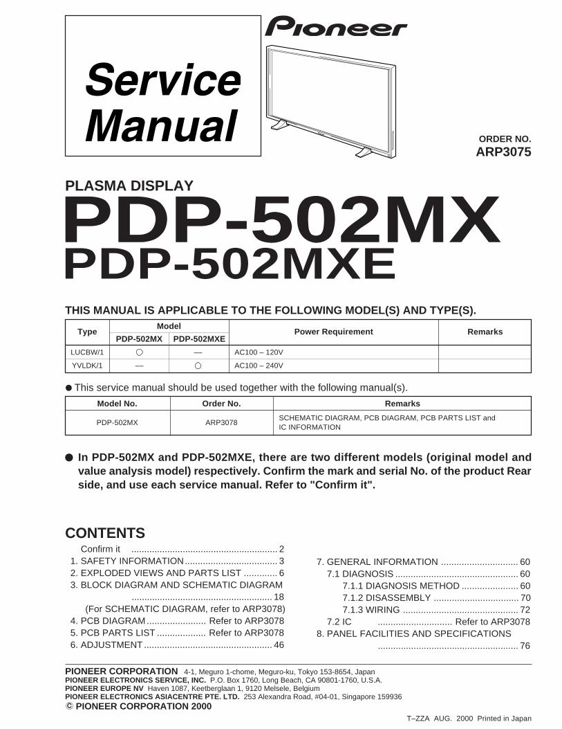
ORDER NO.
PIONEER CORPORATION 4-1, Meguro 1-chome, Meguro-ku, Tokyo 153-8654, JapanPIONEER ELECTRONICS SERVICE, INC. P.O. Box 1760, Long Beach, CA 90801-1760, U.S.A.PIONEER EUROPE NV Haven 1087, Keetberglaan 1, 9120 Melsele, BelgiumPIONEER ELECTRONICS ASIACENTRE PTE. LTD. 253 Alexandra Road, #04-01, Singapore 159936
PIONEER CORPORATION 2000
PDP-502MXEPDP-502MX
Model No. Order No. Remarks
PDP-502MX ARP3078SCHEMATIC DIAGRAM, PCB DIAGRAM, PCB PARTS LIST andIC INFORMATION
PLASMA DISPLAY
ARP3075
T–ZZA AUG. 2000 Printed in Japan
¶ This service manual should be used together with the following manual(s).
LUCBW/1 –– AC100 – 120V
YVLDK/1 –– AC100 – 240V
THIS MANUAL IS APPLICABLE TO THE FOLLOWING MODEL(S) AND TYPE(S).Model
PDP-502MX PDP-502MXEType Power Requirement Remarks
Confirm it ......................................................... 21. SAFETY INFORMATION.................................... 32. EXPLODED VIEWS AND PARTS LIST ............. 63. BLOCK DIAGRAM AND SCHEMATIC DIAGRAM
....................................................... 18(For SCHEMATIC DIAGRAM, refer to ARP3078)
4. PCB DIAGRAM....................... Refer to ARP30785. PCB PARTS LIST ................... Refer to ARP30786. ADJUSTMENT .................................................. 46
CONTENTS
7. GENERAL INFORMATION .............................. 607.1 DIAGNOSIS ................................................ 60
7.1.1 DIAGNOSIS METHOD ...................... 607.1.2 DISASSEMBLY ................................. 707.1.3 WIRING ............................................. 72
7.2 IC ............................. Refer to ARP30788. PANEL FACILITIES AND SPECIFICATIONS
....................................................... 76
In PDP-502MX and PDP-502MXE, there are two different models (original model andvalue analysis model) respectively. Confirm the mark and serial No. of the product Rearside, and use each service manual. Refer to "Confirm it".
PDP-502MX, PDP-502MXE
2
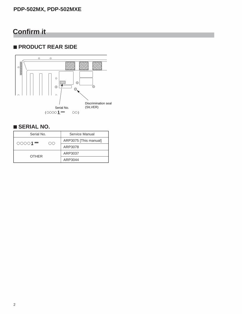
Confirm itConfirm it
Discrimination seal(SILVER)Serial No.
( 1 ∗ ∗ ∗ ∗ ∗ )
SERIAL NO. Serial No. Service Manual
ARP3075 [This manual]
ARP3078
ARP3037 OTHER
ARP3044
PRODUCT REAR SIDE
1 ∗ ∗ ∗ ∗ ∗
PDP-502MX, PDP-502MXE
3
1. SAFETY INFORMATIONThis service manual is intended for qualified service technicians; it is not meant for the casualdo-it-yourselfer. Qualified technicians have the necessary test equipment and tools, and have beentrained to properly and safely repair complex products such as those covered by this manual.Improperly performed repairs can adversely affect the safety and reliability of the product and mayvoid the warranty. If you are not qualified to perform the repair of this product properly and safely, youshould not risk trying to do so and refer the repair to a qualified service technician.
WARNING
This product contains lead in solder and certain electrical parts contain chemicals which are known to the state of California to
cause cancer, bir th defects or other reproductive harm.
Health & Safety Code Section 25249.6 – Proposition 65
1.1 SAFETY PRECAUTIONSNOTICE : Comply with all cautions and safety related notes locatedon or inside the cabinet and on the chassis.The following precautions should be observed :1. When service is required, even though the PDP UNIT an isolation
transformer should be inserted between the power line and theset in safety before any service is performed.
2. When replacing a chassis in the set, all the protective devicesmust be put back in place, such as barriers, nonmetallic knobs,adjustment and compartment covershields, isolation resistor-capacitor, etc.
3. When service is required, observe the original lead dress. Extraprecaution should be taken to assure correct lead dress in thehigh voltage circuitry area.
4. Always use the manufacture's replacement components.Especially critical components as indicated on the circuit diagramshould not be replaced by other manufacture's.Furthermore where a short circuit has occurred, replace thosecomponents that indicate evidence of overheating.
5. Before returning a serviced set to the customer, the servicetechnician must thoroughly test the unit to be certain that it iscompletely safe to operate without danger of electrical shock,and be sure that no protective device built into the set by themanufacture has become defective, or inadvertently defeatedduring servicing. Therefore, the following checks should beperformed for the continued protection of the customer andservice technician.
6. Perform the following precautions against unwanted radiationand rise in internal temperature.• Always return the internal wiring to the original styling.• Attach parts (Ground, Rear Cover, Shield Case) surely after
disassembly.
7. Perform the following precautions for the PDP panel.• When the front case is removed, make sure nothing hits the
panel face, panel corner, and panel edge (so that the glass doesnot break).
• Make sure that the panel vent does not break. (Check that thecover is attached.)
• Handle the FPC connected to the panel carefully.Twisting or pulling the FPC when connecting it to the connectorwill cause it to peel off from the panel.
8. Pay attention to the following.• Be sure to wire the fan. If the fan does not work, the temperature
will rise and cause the protection circuit to operate.• When the front case is removed, infrared ray is radiated and
may disturb reception of the remote control unit.• Pay extreme caution when the front case and rear panel are
removed because this may cause a high risk of disturbance toTVs and radios in the surrounding.
REMARQUE(POUR MODÈLE CANADIEN SEULEMENT)
Les symboles de fusible (fusible de type rapide) et/ou (fusible de type lent) sur CCI indiquent que lespièces de remplacement doivent avoir la même désignation.
NOTICE
(FOR CANADIAN MODEL ONLY)Fuse symbols (fast operating fuse) and/or (slow operating fuse) on PCB indicate that replacement partsmust be of identical designation.
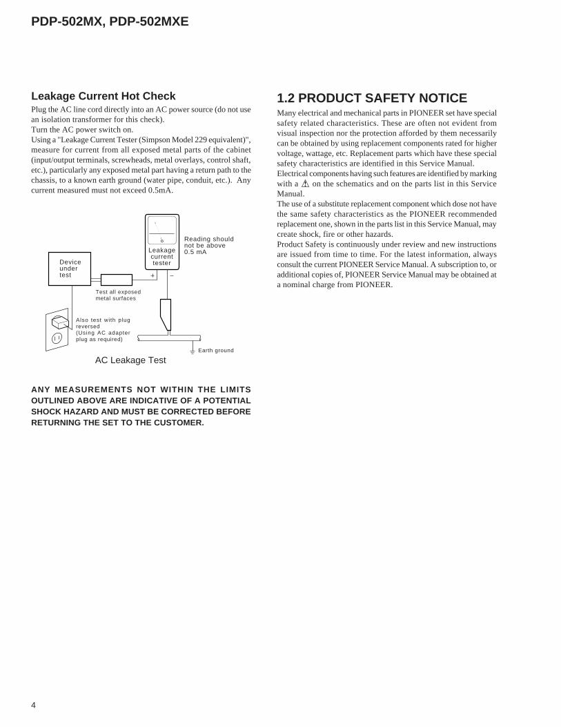
Leakage Current Cold CheckWith the AC plug removed from an AC power source, place ajumper across the two plug prongs. Turn the AC power switch on.Using an insulation tester (DC 500V), connect one lead to thejumpered AC plug and touch the other lead to each exposed metalpart (input/output terminals, screwheads, metal overlays, controlshafts, etc.), particularly any exposed metal part having a returnpath to the chassis. Exposed metal parts having a return path to thechassis should have a minimum resistor reading of 0.3MW and amaximum resistor reading of 5MW. Any resistor value below orabove this range indicates an abnormality which requires correctiveaction. Exposed metal parts not having a return path to the chassiswill indicate an open circuit.
PDP-502MX, PDP-502MXE
4
Leakage Current Hot CheckPlug the AC line cord directly into an AC power source (do not usean isolation transformer for this check).Turn the AC power switch on.Using a "Leakage Current Tester (Simpson Model 229 equivalent)",measure for current from all exposed metal parts of the cabinet(input/output terminals, screwheads, metal overlays, control shaft,etc.), particularly any exposed metal part having a return path to thechassis, to a known earth ground (water pipe, conduit, etc.). Anycurrent measured must not exceed 0.5mA.
ANY MEASUREMENTS NOT WITHIN THE LIMITSOUTLINED ABOVE ARE INDICATIVE OF A POTENTIALSHOCK HAZARD AND MUST BE CORRECTED BEFORERETURNING THE SET TO THE CUSTOMER.
1.2 PRODUCT SAFETY NOTICEMany electrical and mechanical parts in PIONEER set have specialsafety related characteristics. These are often not evident fromvisual inspection nor the protection afforded by them necessarilycan be obtained by using replacement components rated for highervoltage, wattage, etc. Replacement parts which have these specialsafety characteristics are identified in this Service Manual.Electrical components having such features are identified by markingwith a on the schematics and on the parts list in this ServiceManual.The use of a substitute replacement component which dose not havethe same safety characteristics as the PIONEER recommendedreplacement one, shown in the parts list in this Service Manual, maycreate shock, fire or other hazards.Product Safety is continuously under review and new instructionsare issued from time to time. For the latest information, alwaysconsult the current PIONEER Service Manual. A subscription to, oradditional copies of, PIONEER Service Manual may be obtained ata nominal charge from PIONEER.
Also test with plugreversed(Using AC adapterplug as required)
Deviceundertest
Test all exposedmetal surfaces
Earth ground
Leakagecurrenttester
Reading shouldnot be above0.5 mA
AC Leakage Test
PDP-502MX, PDP-502MXE
5
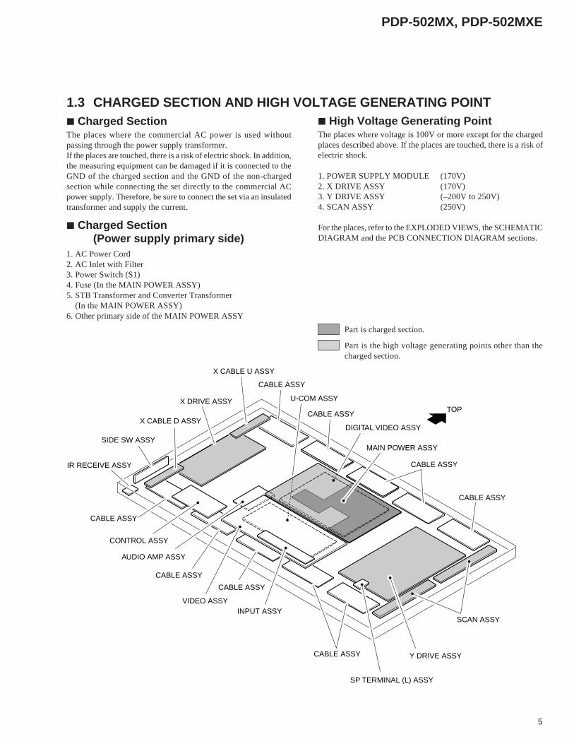
7 Charged SectionThe places where the commercial AC power is used withoutpassing through the power supply transformer.If the places are touched, there is a risk of electric shock. In addition,the measuring equipment can be damaged if it is connected to theGND of the charged section and the GND of the non-chargedsection while connecting the set directly to the commercial ACpower supply. Therefore, be sure to connect the set via an insulatedtransformer and supply the current.
1.3 CHARGED SECTION AND HIGH VOLTAGE GENERATING POINT
7 Charged Section(Power supply primary side)
1. AC Power Cord2. AC Inlet with Filter3. Power Switch (S1)4. Fuse (In the MAIN POWER ASSY)5. STB Transformer and Converter Transformer (In the MAIN POWER ASSY)6. Other primary side of the MAIN POWER ASSY
7 High Voltage Generating PointThe places where voltage is 100V or more except for the chargedplaces described above. If the places are touched, there is a risk ofelectric shock.
1. POWER SUPPLY MODULE (170V)2. X DRIVE ASSY (170V)3. Y DRIVE ASSY (–200V to 250V)4. SCAN ASSY (250V)
For the places, refer to the EXPLODED VIEWS, the SCHEMATICDIAGRAM and the PCB CONNECTION DIAGRAM sections.
Part is the high voltage generating points other than thecharged section.
Part is charged section.
INPUT ASSYVIDEO ASSY
AUDIO AMP ASSY
CONTROL ASSY
DIGITAL VIDEO ASSY
X CABLE U ASSY
X CABLE D ASSY
SIDE SW ASSY
IR RECEIVE ASSY
SCAN ASSY
CABLE ASSY
CABLE ASSY
CABLE ASSY
CABLE ASSY
CABLE ASSY
SP TERMINAL (L) ASSY
CABLE ASSY
CABLE ASSY
CABLE ASSY
U-COM ASSY
MAIN POWER ASSY
TOPX DRIVE ASSY
Y DRIVE ASSY
PDP-502MX, PDP-502MXE
6
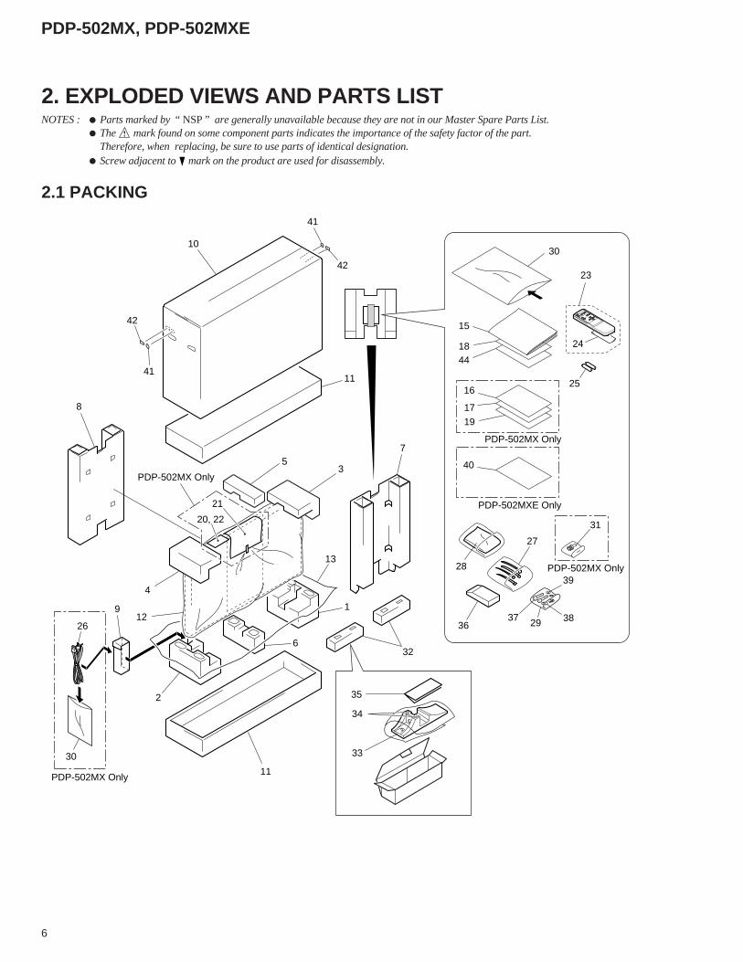
2. EXPLODED VIEWS AND PARTS LIST
2.1 PACKING
NOTES : Parts marked by “ NSP ” are generally unavailable because they are not in our Master Spare Parts List.The mark found on some component parts indicates the importance of the safety factor of the part.Therefore, when replacing, be sure to use parts of identical designation.Screw adjacent to mark on the product are used for disassembly.
41
41
21
32
35
33
34
8
10
4
3
11
75
9
PDP-502MX Only
PDP-502MX Only
PDP-502MX Only
PDP-502MXE Only
PDP-502MX Only
2
11
30
6
1
13
1226
20, 22
15
23
28
40
27
31
24
25
30
3637 29 38
39
1844
16
17
19
42
42
PDP-502MX, PDP-502MXE
7
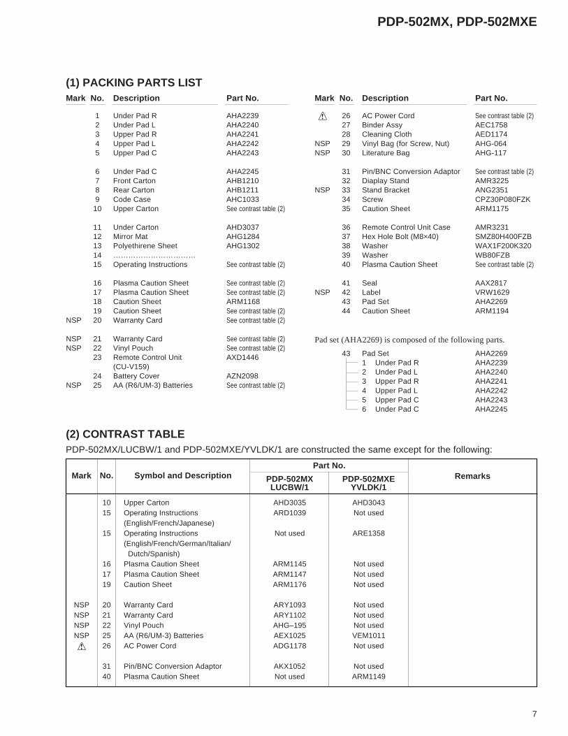
10 Upper Carton AHD3035 AHD304315 Operating Instructions ARD1039 Not used
(English/French/Japanese)15 Operating Instructions Not used ARE1358
(English/French/German/Italian/ Dutch/Spanish)
16 Plasma Caution Sheet ARM1145 Not used17 Plasma Caution Sheet ARM1147 Not used19 Caution Sheet ARM1176 Not used
NSP 20 Warranty Card ARY1093 Not usedNSP 21 Warranty Card ARY1102 Not usedNSP 22 Vinyl Pouch AHG–195 Not usedNSP 25 AA (R6/UM-3) Batteries AEX1025 VEM1011
26 AC Power Cord ADG1178 Not used
31 Pin/BNC Conversion Adaptor AKX1052 Not used40 Plasma Caution Sheet Not used ARM1149
(1) PACKING PARTS LISTMark No. Description Part No.
(2) CONTRAST TABLEPDP-502MX/LUCBW/1 and PDP-502MXE/YVLDK/1 are constructed the same except for the following:
Mark PDP-502MX PDP-502MXELUCBW/1 YVLDK/1
Part No.RemarksSymbol and DescriptionNo.
1 Under Pad R AHA22392 Under Pad L AHA22403 Upper Pad R AHA22414 Upper Pad L AHA22425 Upper Pad C AHA2243
6 Under Pad C AHA22457 Front Carton AHB12108 Rear Carton AHB12119 Code Case AHC1033
10 Upper Carton See contrast table (2)
11 Under Carton AHD303712 Mirror Mat AHG128413 Polyethirene Sheet AHG130214 ……………………………15 Operating Instructions See contrast table (2)
16 Plasma Caution Sheet See contrast table (2)17 Plasma Caution Sheet See contrast table (2)18 Caution Sheet ARM116819 Caution Sheet See contrast table (2)
NSP 20 Warranty Card See contrast table (2)
NSP 21 Warranty Card See contrast table (2)NSP 22 Vinyl Pouch See contrast table (2)
23 Remote Control Unit AXD1446(CU-V159)
24 Battery Cover AZN2098NSP 25 AA (R6/UM-3) Batteries See contrast table (2)
26 AC Power Cord See contrast table (2)27 Binder Assy AEC175828 Cleaning Cloth AED1174
NSP 29 Vinyl Bag (for Screw, Nut) AHG-064NSP 30 Literature Bag AHG-117
31 Pin/BNC Conversion Adaptor See contrast table (2)32 Diaplay Stand AMR3225
NSP 33 Stand Bracket ANG235134 Screw CPZ30P080FZK35 Caution Sheet ARM1175
36 Remote Control Unit Case AMR323137 Hex Hole Bolt (M8×40) SMZ80H400FZB38 Washer WAX1F200K32039 Washer WB80FZB40 Plasma Caution Sheet See contrast table (2)
41 Seal AAX2817NSP 42 Label VRW1629
43 Pad Set AHA226944 Caution Sheet ARM1194
Mark No. Description Part No.
Pad set (AHA2269) is composed of the following parts.
43 Pad Set AHA22691 Under Pad R AHA22392 Under Pad L AHA22403 Upper Pad R AHA22414 Upper Pad L AHA22425 Upper Pad C AHA22436 Under Pad C AHA2245
PDP-502MX, PDP-502MXE
8
3
11
1
15
14
4
4
9
7
32
7
22
20
21
27 (MXE)
27 (MX)
17 10
10
9
PDP-502MXOnly
PDP-502MXOnly
PDP-502MX Only
PDP-502MXOnly
PDP-502MXEOnly
PDP-502MXEOnly
4
4
4
10
10
10
10
10
4
4
9
9
9
99
9 28
9
94
54
912
12
31
29
4
4
4
8
18
19 (MX)30 (MXE)
16
25
13
26
6
33
Refer to "2.3 EXTERIOR (1/3)".
24
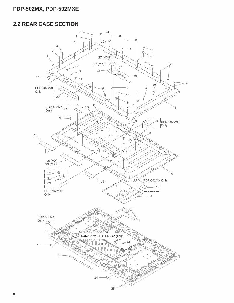
2.2 REAR CASE SECTION
PDP-502MX, PDP-502MXE
9
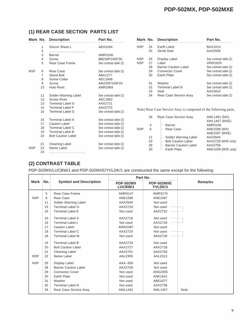
1 Siricon Sheet L AEH10342 ……………………………3 Barrier AMR31664 Screw BBZ40P160FZK5 Rear Case Frame See contrast table (2)
NSP 6 Rear Case See contrast table (2)7 Stand Bolt ABA12778 Screw Collar AEC18489 Screw AMZ30P100FZK
10 Hole Rivet AMR2969
11 Solder Warning Label See contrast table (2)12 Screw Rivet AEC185213 Terminal Label D AAX272114 Terminal Label F AAX272315 Terminal Label G See contrast table (2)
16 Terminal Label A See contrast table (2)17 Caution Label See contrast table (2)18 Terminal Label C See contrast table (2)19 Terminal Label B See contrast table (2)20 Bolt Caution Label See contrast table (2)
21 Cleaning Label See contrast table (2)NSP 22 Name Label See contrast table (2)
23 ……………………………
Mark No. Description Part No.
(1) REAR CASE SECTION PARTS LIST
5 Rear Case Frame AMR3147 AMR3170NSP 6 Rear Case ANE1596 ANE1587
11 Solder Warning Label AAX2644 Not used15 Terminal Label G AAX2724 Not used15 Terminal Label E Not used AAX2722
16 Terminal Label A AAX2718 Not used16 Terminal Label L Not used AAX273417 Caution Label ARW1087 Not used18 Terminal Label C AAX2720 Not used18 Terminal Label M Not used AAX2735
19 Terminal Label B AAX2719 Not used20 Bolt Caution Label AAX2727 AAX272821 Cleaning Label AAX2751 AAX2766
NSP 22 Name Label AAL2309 AAL2313
NSP 26 Display Label AAX–359 Not used28 Barrier Caution Label AAX2759 Not used29 Connector Cover Not used ANG235530 Earth Plate Not used ANK164131 Washer Not used ABE107732 Terminal Label N Not used AAX273634 Rear Case Service Assy AWL1461 AWL1457 Note
(2) CONTRAST TABLEPDP-502MX/LUCBW/1 and PDP-502MXE/YVLDK/1 are constructed the same except for the following:
Mark PDP-502MX PDP-502MXELUCBW/1 YVLDK/1
Part No.RemarksSymbol and DescriptionNo.
NSP 24 Earth Label BAX101425 Serial Seal AAX2609
NSP 26 Display Label See contrast table (2)NSP 27 Label VRW1629
28 Barrier Caution Label See contrast table (2)29 Connector Cover See contrast table (2)30 Earth Plate See contrast table (2)
31 Washer See contrast table (2)32 Terminal Label N See contrast table (2)33 Seal AAX281634 Rear Case Service Assy See contrast table (2)
Mark No. Description Part No.
Note) Rear Case Service Assy is composed of the following parts.
34 Rear Case Service Assy AWL1461 (MX)AWL1457 (MXE)
3 Barrier AMR3166NSP 6 Rear Case ANE1596 (MX)
ANE1587 (MXE)11 Solder Warning Label AAX264420 Bolt Caution Label AAX2728 (MXE only)28 Barrier Caution Label AAX275930 Earth Plate ANK1639 (MXE only)
PDP-502MX, PDP-502MXE
10
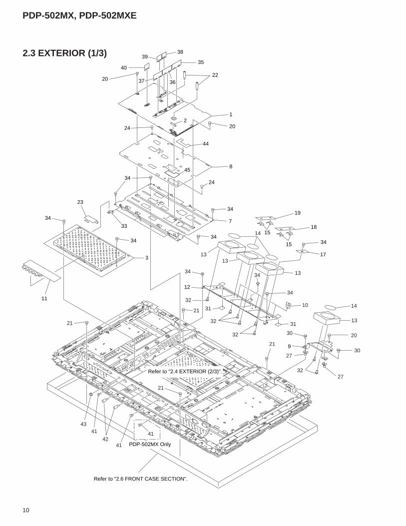
2.3 EXTERIOR (1/3)
23
7
8
44
45
1
22
20
20
40
37
3839
35
36
242
10
30
30
34
3434
13
20
27
27
21
21
21
21
41
4142
4143
31
32
13
1313
14
14
12
34
34
34
34
34
33
3
9
17
34
19
18
15
15
31
32
32
3211
24
Refer to "2.4 EXTERIOR (2/3)".
Refer to "2.6 FRONT CASE SECTION".
PDP-502MX Only
PDP-502MX, PDP-502MXE
11
1 MAIN POWER ASSY AWZ65062 Fuse (10A, FU101) AEK10713 VIDEO ASSY See contrast table (2)4 ……………………………5 ……………………………
6 ……………………………NSP 7 Chassis ANA1605
8 Insulating Sheet AMR31999 Fan Frame A ANG2330
10 Wire Saddle AEC1745
11 INPUT ASSY AWZ6496NSP 12 Fan Frame C ANG2393
13 Fan Motor AXM103614 Fan Label AAX278515 Locking Card Spacer AEC1736
16 ……………………………17 SENSOR (A) ASSY AWZ650118 FAN CABLE (A) ASSY AWZ650219 FAN CABLE (B) ASSY AWZ649720 Screw BMZ30P060FCU
21 Screw BBZ40P160FZK22 Spacer Screw AEF102823 Wire Barrier AMR320924 Nylon Rivet AEC167125 ……………………………
26 ……………………………27 PCB Mold AMR211528 ……………………………29 ……………………………30 Screw ABZ30P160FCU
31 Fan Angle Cushion AED119332 Screw PPZ50P100FZK33 PCB Hinge AEC180734 Screw AMZ30P060FMC35 RCC CONTROL A ASSY AWZ6507
36 RCC CONTROL B ASSY AWZ650837 RCC CONTROL C ASSY AWZ650938 OTL CONTROL A ASSY AWZ651039 OTL CONTROL B ASSY AWZ651140 OTL CONTROL C ASSY AWZ6512
41 Screw BPZ30P080FZK42 Hexagon Screw BBA105143 Nut ABN103344 Insulation Sheet S AMR323345 Insulation Sheet L AMR3234
Mark No. Description Part No.
(1) EXTERIOR (1/3) SECTION PARTS LIST
Mark No. Description Part No.
3 VIDEO ASSY AWZ6495 AWZ6516
(2) CONTRAST TABLEPDP-502MX/LUCBW/1 and PDP-502MXE/YVLDK/1 are constructed the same except for the following:
Mark PDP-502MX PDP-502MXELUCBW/1 YVLDK/1
Part No.RemarksSymbol and DescriptionNo.
PDP-502MX, PDP-502MXE
12
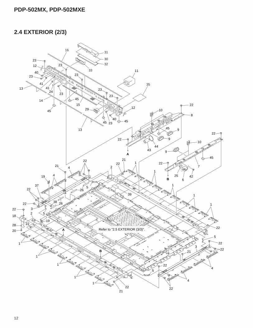
2.4 EXTERIOR (2/3)
45
5
22
22
22
22
5
21
22
3
4
4
1631
33
30
32
35
15
12
40
40
4141
23
23
23
24
45
2323
13
14
13
29 12
11
23
23
23
10
8
9
4344
9
9
10
7
256
42
5
2639
2638
5
3
2237
22
4
4
2222
222
22
21
21
1
1
1
1
1
2221
1
1
1
1
1
2
19
20
28
18
22
22
B
A
A
B
22
22
19
45 45
45
45
Refer to "2.5 EXTERIOR (3/3)".
PDP-502MX, PDP-502MXE
13
1 Frame Shield H ANK16092 Frame H ANG23963 Frame V ANG23444 Frame Shield V ANK16105 Corner Holder ANG2347
6 Ferrite Core (L1) ATX10377 Sub Frame R ANG23958 Sub Frame L ANG24199 Bush C AEC1740
10 Wire Saddle AEC1745
11 AC Inlet with Filter (CN1) See contrast table (2)12 Shield Gasket B ANK164613 Shield Gasket D See contrast table (2)14 Shield Gasket C ANK164715 Terminal Panel See contrast table (2)
16 Shield Gasket E See contrast table (2)17 ……………………………
NSP 18 IR Holder ANG234619 Edging Saddle AEC173720 Nylon Rivet AEC1671
21 Screw AMZ30P080FCU22 Screw AMZ30P060FMC23 Screw BMZ30P060FCU24 Hexagon Screw BBA105125 Ferrite Core Holder AEC1818
26 FPC Cushion AEB134127 ……………………………28 IR RECEIVE ASSY AWZ649829 Power Switch (S1) BSM100630 CONTROL ASSY AWZ6504
NSP 31 Control Shield Case ANK1626NSP 32 Control Shield Cover ANK1627NSP 33 Control Shield Plate ANG2380
34 ……………………………35 SP TERMINAL (L) ASSY AWZ6505
36 ……………………………37 Spacer AEC184738 Screw AMZ30P100FZK
NSP 39 Drive Voltage Label ARW109740 Screw BPZ30P080FZK
41 Nut ABN103342 Screw PMB40P080FMC43 Ferrite Core (L2) ATX103144 Binder AEC185145 Dust Guard AEB1362
11 AC Inlet with Filter (CN1) AKP1210 AKP120913 Shield Gasket D ANK1648 ANK161415 Terminal Panel ANG2341 ANG235316 Shield Gasket E ANK1649 ANK1634
(2) CONTRAST TABLEPDP-502MX/LUCBW/1 and PDP-502MXE/YVLDK/1 are constructed the same except for the following:
Mark PDP-502MX PDP-502MXELUCBW/1 YVLDK/1
Part No.RemarksSymbol and DescriptionNo.
Mark No. Description Part No.
(1) EXTERIOR (2/3) SECTION PARTS LIST
Mark No. Description Part No.
PDP-502MX, PDP-502MXE
14
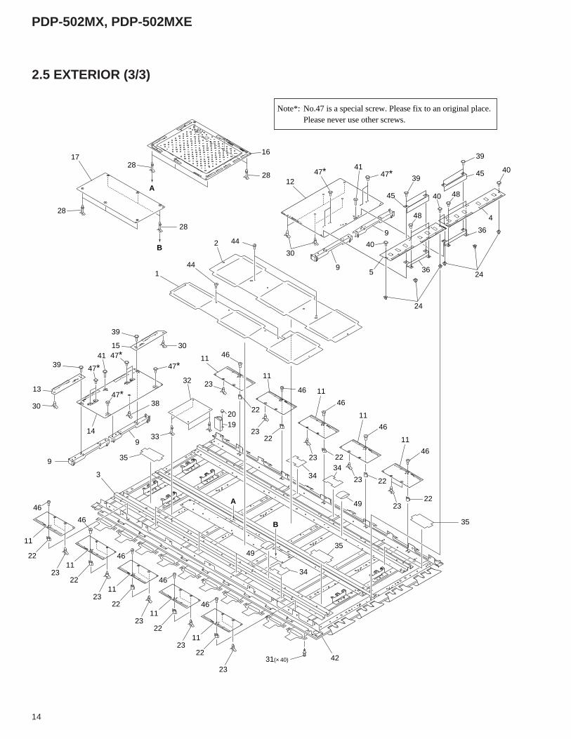
2.5 EXTERIOR (3/3)
A
A
B
B
22
11
46
23
42
2223
46
11
31(× 40)
35
35
34
49
34
34
49
3
359
30
30
13
14
44
44
30
28
2828
1617
28
39
39
1
2
15
47∗47∗47∗
47∗38
41
9
32
33
2019
2223
46
24
36
36
24
4
5
40
40 48
45
45
39
39
48
40
9
9
11
2223
46
11
2223
46
11
22
23
4611
47∗41
47∗12
22
11
46
23
22
11
46
23
22
11
46
23
22
11
46
23
Note*: No.47 is a special screw. Please fix to an original place. Please never use other screws.
PDP-502MX, PDP-502MXE
15
NSP 1 Panel Shield S ANK1633NSP 2 Panel Shield L ANK1632NSP 3 Frame Assy ANA1633
4 SCAN (A) ASSY AWZ65185 SCAN (B) ASSY AWZ6519
6 ……………………………7 ……………………………8 ……………………………9 PCB Spacer AMR3155
10 ……………………………
11 CABLE ASSY AWV184312 Y DRIVE ASSY AWV184713 X CABLE D ASSY AWZ651514 X DRIVE ASSY AWV184215 X CABLE U ASSY AWZ6514
16 DIGITAL VIDEO ASSY AWV184117 UCOM ASSY See contrast table (2)18 ……………………………
NSP 19 Tube Cover AMR3036NSP 20 Push Rivet AEC1748
21 ……………………………22 Dust Guard Collar AMR322723 Locking Spacer AEC179424 Screw Grommet AEC185725 ……………………………
NSP 26 ……………………………27 ……………………………
NSP 28 Circuit Board Spacer AEC174429 ……………………………30 Locking Spacer AEC1796
31 Plastic Rivet AMR106632 AUDIO AMP ASSY AWZ6503
NSP 33 PCB Spacer AEC1446NSP 34 Blind Sheet S AMR3202NSP 35 Blind Sheet L AMR3203
NSP 36 Hot Plate ANG241637 ……………………………38 Circuit Board Spacer AEC179539 Screw ABZ30P160FCU40 Screw BBZ40P120FZK
41 Screw IBZ30P250FCUNSP 42 Plasma Panel Assy AAV1236
43 ……………………………44 Screw ABZ30P060FCU45 Hot Plate Barrier AMR3223
46 Screw ABA105647 Screw ABA120048 Screw ABZ30P060FCU49 Ferrite Core (L4, L5) ATX1041
17 UCOM ASSY AWZ6499 AWZ6520
(2) CONTRAST TABLEPDP-502MX/LUCBW/1 and PDP-502MXE/YVLDK/1 are constructed the same except for the following:
Mark PDP-502MX PDP-502MXELUCBW/1 YVLDK/1
Part No.RemarksSymbol and DescriptionNo.
Mark No. Description Part No.
(1) EXTERIOR (3/3) SECTION PARTS LIST
Mark No. Description Part No.
PDP-502MX, PDP-502MXE
16
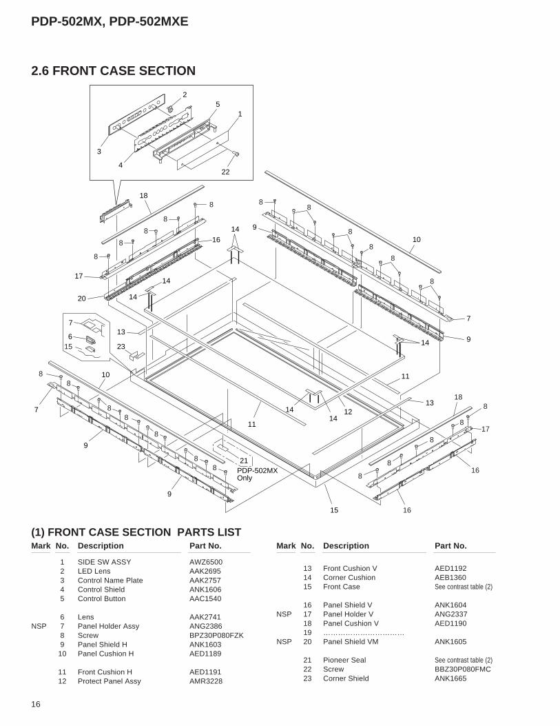
2.6 FRONT CASE SECTION
8
8
8
17
16
16
18
8
8
8
8
8
8
888
8
8
8
8
8
15
8
8
8
8
8
13
11
7
9
9
13
15
7
6
7
9
9
PDP-502MXOnly
3
2
224
51
121414
14
14
17
14
14
11
20
16
18
10
10
21
8
23
1 SIDE SW ASSY AWZ65002 LED Lens AAK26953 Control Name Plate AAK27574 Control Shield ANK16065 Control Button AAC1540
6 Lens AAK2741NSP 7 Panel Holder Assy ANG2386
8 Screw BPZ30P080FZK9 Panel Shield H ANK1603
10 Panel Cushion H AED1189
11 Front Cushion H AED119112 Protect Panel Assy AMR3228
Mark No. Description Part No.
(1) FRONT CASE SECTION PARTS LIST
13 Front Cushion V AED119214 Corner Cushion AEB136015 Front Case See contrast table (2)
16 Panel Shield V ANK1604NSP 17 Panel Holder V ANG2337
18 Panel Cushion V AED119019 ……………………………
NSP 20 Panel Shield VM ANK1605
21 Pioneer Seal See contrast table (2)22 Screw BBZ30P080FMC23 Corner Shield ANK1665
Mark No. Description Part No.
PDP-502MX, PDP-502MXE
17
15 Front Case AMB2649 AMB267921 Pioneer Seal ARW1091 Not used
(2) CONTRAST TABLEPDP-502MX/LUCBW/1 and PDP-502MXE/YVLDK/1 are constructed the same except for the following:
Mark PDP-502MX PDP-502MXELUCBW/1 YVLDK/1
Part No.RemarksSymbol and DescriptionNo.
2.7 PDP SERVICE ASSY (AWU1030)PDP SERVICE ASSY (AWU1030) is composed of the following parts.Please refer to 2.4 and 2.5 for the illustrations of each part.
2.4 EXTERIOR (2/3)1 Frame Shield H ANK16092 Frame H ANG23963 Frame V ANG23444 Frame Shield V ANK16105 Corner Holder ANG2347
21 Screw AMZ30P080FCU22 Screw AMZ30P060FMC26 FPC Cushion AEB134137 Spacer AEC184738 Screw AMZ30P100FZK
NSP 39 Drive Voltage Label ARW1097
2.5 EXTERIOR (3/3)NSP 3 Frame Assy ANA1633NSP 19 Tube Cover AMR3036NSP 20 Push Rivet AEC1748
23 Locking Spacer AEC179424 Screw Grommet AEC1857
NSP 28 Circuit Board Spacer AEC174430 Locking Spacer AEC179631 Plastic Rivet AMR1066
NSP 33 PCB Spacer AEC1446NSP 34 Blind Sheet S AMR3202
NSP 35 Blind Sheet L AMR320338 Circuit Board Spacer AEC1795
NSP 42 Plasma Panel Assy AAV1236
Mark No. Description Part No. Mark No. Description Part No.
OTHERSWire Saddle AEC1797Flat Clamp AEC1858Cable Clip AEC1859
NSP FPC (XGA2-Y) ADY1047NSP FPC (XGA2-X) ADY1053NSP Address Mojule (IC21–IC40) MC-16340
PACKINGButton Bolt ABA1259Corner Pad AHA2203Corner Carton AHA2204Upper Carton AHD2970Under Carton AHD2971
Packing Sheet AHG1291Holder Plate AHK1008Washer WB80FZB
PDP-502MX, PDP-502MXE
18
A
B
C
D
1 2 3 4
1 2 3 4
CABLE ASSY
K1K2
CABLE ASSY
K1K2
CABLE ASSY
K1K2
E17
E7
E12 E10
E8
E22E15
E16E1
E19 E2
E5E3
E35 E6
E3
E2
E
E21
E24
E23
EEPROMIC3601
S5V
S5V14V
E33
RST
REG
R5V
SYSTEMCONT CPU
IC3604
PWR
U-COM ASSY
E18
Vsus
SUSOUT
Psu
s(X
)
F7
Psu
s(X
)
X DRIVE ASSY
To
Pan
el X
-Ele
ctro
de
Vsus12V
SustainPulse Gen.
IC3405
SustainPulse Gen.
IC3402
Vsus12V5V
5V
To
Pan
el X
-Ele
ctro
de
SUSOUT
F5
Vsus
F6
12V
5V
+RST OUT
Psu
s(X
)
RST
SUS
5V
DRVSig.
LogicBLK
OC
PD
Isol
atio
n (P
C)
BLK
+ Reset Pulse Gen.
PD CONTRelay
AC IN
Vad
r
Vsu
s
PD
STB5V
HI PWROFF SW
STB12V
MAIN POWER ASSY
P1
P4
P6
P3
P5
P7
FU101
+B
STBYPWR
PWR
DELAYDELAY
VSUSSW PWR
Vsu
s10
V
VADRSW PWR
12V
8V 14V
PFC
-8V
OCOVC
PD
VCCSW PWR
RGBDAT
RG
B D
AT
HD
,VD
D4
D1
D19
D18
D12
D13
D
D20 D22
CL
IPProcess
CLP PulseGen.
CABLE ASSY
CONTROLASSY
CABLE ASSY
AUDIO AMP ASSY A33 A35
A19
A20
A1
A2
A3
A5
SVDRPr
HDCS
GY
BPb
RGBOUT
RGBIn
IN 3IN 4
RGBDecoderIC1401
In3/In4SEL
YCbC
YPbP
HDVD
YPbPr
Y
RGB
RGB
P&P
SyncSepa
G/Y
HDVD
HD,VD
VD
HD
HD
HD
CLK
CLK
V.ROMRGB
502MXEOnly
SyncU-ComF-DET
CLP,HVBLK
CLP,HVBLK
Sync
IC2402AMP/AD/PLL
SELCONT
DATCLK
A17
A30
-5APLL5VBPLL
9V_PIC9V_SIG
RE
12V
SEL
Audio1/2
Audio3/4
LRLR
12V
CABLE ASSY
B2 B3
12V
15VD-D CON
PWR AMPIC4502
DC DET
PD
R L
12VSTB5V LR V
OL
13V
MUTE
VOL CONT(Main/Sub) LR
R10V
REG
14V
FANDRV
14V
FANCONTBLK
SENSSD
FANMAX
OS
D D
AT
SIDE SWASSY
KEY, LED
12V5V
5V
5V
Vadr Vadr
VadrVadr
Vsus
Vsus
5V
C6 C5 C4 C2
C1
U1
S1
R OUT AudioOut
CombiIn Out
SRIn
SROut
IRRECEIVE
ASSY TxRx
REM
LR
12V
R
S5VPD, VOL
13V,S5V
K1 K2 K1 K2 K1 K2
SDet
REM, Tx, Rx,Vol, Mute
PD
13V DAT, CLKSDet, FDet
SDASCK
RG
B(A
), (
B)
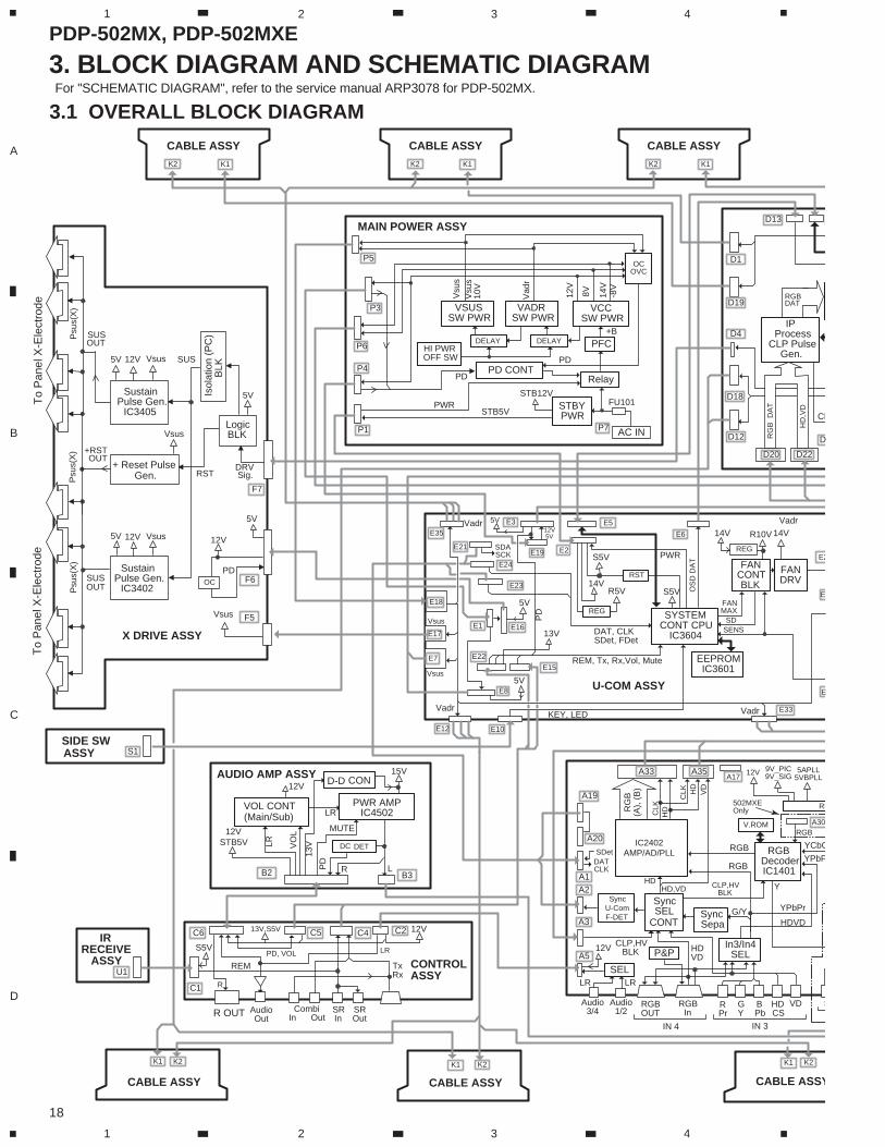
3. BLOCK DIAGRAM AND SCHEMATIC DIAGRAM
3.1 OVERALL BLOCK DIAGRAMFor "SCHEMATIC DIAGRAM", refer to the service manual ARP3078 for PDP-502MX.
PDP-502MX, PDP-502MXE
19
A
B
C
D
5 6 7 8
5 6 7 8
VHIC5V
ADDSEL
PULSE
VHIC5V
ADDSEL
PULSE
VHIC5V
ADDSEL
PULSE
VHIC5V
ADDSEL
PULSE
VHIC5V
ADDSEL
PULSE
VHIC5V
ADDSEL
PULSE
CABLE ASSY
K1K2
E38
E26
E27
E33 To
Pan
el Y
-Ele
ctro
deT
o P
anel
Y-E
lect
rode
DIGITAL VIDEO ASSY
RGBDAT
DRVSig
TOP ADR DAT(64bit * RGB * 20)
Sub-FieldConv.
* Field MEM
IP CPU
PanelCPU
RG
B D
AT
HD
,VD
XY DRVSequencepattern
Gen.
RGBDAT
D16D11
D3D5
D7
D9
D8
D10
9
8
2
D6D13 D14
D17
D20 D22
CLP
5V3.3V
12V
IPProcess
CLP PulseGen.
RGBDAT
AspectConv.FIFO
Gamma-1ABL
DitherOSD Add
OSDGen
Xtal60M
Xtal50M
BOTTOM ADR DAT(64bit * RGB * 20)
VA
DR
Con
t
REG
OCUPV
PD
20
20
V/Y
3DY/Y/SY SEL
C
C SEL
3D Y/C forNTSC
3Line Y/Cfor
PAL/60PALV/Y
C
NTFIL
PALFIL
3DY Y
3DC
PA
LY
SE
C Y
C C
Y SEL C SEL
SDAT
CONT
SERPARACONV.
BW_YSECFIL
FILTER
Y
CABLE ASSY CABLE ASSY CABLE ASSY
A13 VIDEO ASSY5V_PIC5_PLD
5V_RGB
OUTVBSYCSVDHDCS
GY
BPb IN 1IN 2
IN 3
In1/In2SEL V/Y
C
Y, Col diff Decoder
Y,C
SyncSepa
RGBDecoderIC1401
/In4EL
YCbCr
YPbPr
HDVD
YPbPrY
Y IC1201
GB
B
YSyncSEL
V.ROMRGB
2MXEnly
502MX Only
SCL, SDA
A30 A31
13V, 8V, -8V
-5V_IO5V_AD
5APLL5VBPLL
9V_PIC9V_SIG
REG
12V
Vsus12V
Vsus12V
5V
5V
Vsus
H4
Vsus10V
VRN
VH
Vofs
Vsus
IC5V VFZ
14V
-8V
SustainPulse Gen.
IC3702
SU
S O
UT
SustainPulse Gen.
IC3707S
US
OU
T
Vcp
-RST
OFS
VRN
- Reset Pulse Gen.
OFSPulse Gen.
Vofs
5V
H5
H1
VcpBLK
Vcp
12V
SU
SS
US
OVP
D-DCONVBLK
OC
-8V
12V
CPMSK
OFS
Vsus10V
UVPOVP
14V
PD
5V
DRV Sig.
D-D CONVBLK
CP
MS
K, O
FS
VHIC5V
ADDSEL
PULSE
VHIC5V
ADDSEL
PULSE
VHIC5V
ADDSEL
PULSE
Psu
s(Y
)P
sus(
Y)
Y-SUSMASKBLK
SI ,CLK
VHIC5V
ADDSEL
PULSE
VHIC5V
ADDSEL
PULSE
VHIC5V
ADDSEL
PULSE
H2
V10
V9
V8
V11
V12
V13
H3
Y DRIVE ASSY
Psu
s(Y
)
RN
VHIC5V
VHIC5V
LogicBLK
SP(L)ASSY
L OUT
TEMPSENS
IC4101
SENSOR A ASSY
SENS A
R10V
SENS
FAN CABLE AASSY
FAN CABLE BASSY
FAN A
FAN B
FAN C
FAN D
FANDRV A
FANDRV B
FANDRV B
R10V
EG
FANDRV
14V
FANCONTBLK
S
Vadr
Vadr
K1 K2 K1 K2 L1 K2K1
CABLE ASSY
SCAN (A) ASSY
SCAN (B) ASSY
K1
K2
ADRU/B/D/G
VADR
IC IC IC IC
VADR
IC IC IC IC
VADR
DEF DEF DEF DEF
DA
T3
(64b
it)
RG
BR
GB
RG
B
RG
B
RG
B
RG
B
RG
B
RGB
CLKB CLKBCLK CLKVADRGen.
12V5V
3.3V
DA
T2
(64b
it)
DA
T1
(64b
it)
DA
T0
(64b
it)
V14
V7
V6
V5
V4
V3
V2
V1
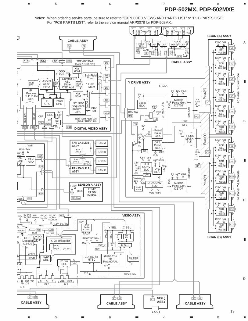
Notes: When ordering service parts, be sure to refer to "EXPLODED VIEWS AND PARTS LIST" or "PCB PARTS LIST".For "PCB PARTS LIST", refer to the service manual ARP3078 for PDP-502MX.
PDP-502MX, PDP-502MXE
20
A
B
C
D
1 2 3 4
1 2 3 4
IC305
2MHz
IC1207
VIDEO SWIC306
(BA7657F)
Multi Component ProcessorRGB Matrix
IC1401(CXA2101AQ)
RGB DECODER
LPF
Y/G 2
Pb/BPr/R
FS
C
HB
LK_C
NR
CLP
_CN
R Y C
SC
L
SD
A
HD/CSVD
4
6
8
10
INP
UT
3 (R
GB
1)
INPUT ASSY(AWZ6496)
To CONTROL ASSY CN4703
RG
B2
INR
GB
2 O
UT
AU
DIO
INP
UT2
(502
MX
)IN
PU
T4 (5
02M
XE
)
AU
DIO
INP
UT1
(502
MX
)IN
PU
T3 (5
02M
XE
)
INP
UT
1IN
PU
T2
CN35062
1
410 6 1 56951
27
45
1
2
4
5
11
1213
3 R
R
L
R
LL14
15
1
2
4
5
11
12
14
15
42
Y
C
3
5
5
7976 75
4
3
11
10
9
7
55 56 31 43
8
EXT_Y
INT_Cr
INT_Cb
INT_Y
EXT_Pb
EXT_Pr
EXT_HD
EXT_VD
SC
L
SD
A
SC
P P_ACL
24
12
4
6
8
10
CN303
7
G
7
4
4
7
1
10
HO
UT
SD
A
SC
L
SY
NC
B
R
HD
VD
9
11
23
13
G1
S_DET
S2_DET
B1
R1
HD1
VD1
G2
B2
21
9
12
5
6
3
2
37
36
35
Y
B–Y
Y SYNC
Y
RGB SYNC
R–Y
710
1
5
3
19
15
22
14
R2
HD2
VD2
R
G
B
IC1204(BA7655AF)
IC506
IC303
Comp
12V
Reg
IC301
Comp
S2_DET
S_DET
IC503
Comp
IC501
Comp
IC1205(NJN1319M)
Comp
Comp
IC507(24LCS21A)
5V_RGB
SCL
VCLK
SDA
HD
VD
Plug & PlayROM
+5V_RGB
9V_PIC
R
15
12
10
G
B HD
VD
2
5
7
12V
9V Reg
9V_S
IG
9V Reg
9V_P
IC
5V Reg
5V_R
GB
5V Reg
5V_P
IC
5V Reg
5V_P
LD
5V Reg
+5A
_PLL
+5D
_PLL
5V Reg
+5A
D
–5V
Reg
–5V
_IO
3.3V
Reg
+3.
3AD
IC1202(TC74HC4538AF)
HBLK Gen.
Y/B–Y/R–Y DECODER SYNC SEPA.TV JUNGLE IC
IC1201(TB1227BW)
SCP Gen.
SHP_SWMAI_SW
FN
C_0
FNC_1
FNC_2 MR_V_SW
1 3
CN302A5
1 2 5 6 7 11CN3401
80
37
39
35
5V_PIC9V_SIG
IC651
IC102
5V_PIC
K1404
SAND CASTLE PULSE GEN.HBLK/VBLK/CLP added
K2013HBLK
K2023HD3
K2024VD3
K2025HD4
K2026VD4
K2014VBLK
4
3
INPUT
OUTPUT
Y
C
SINC
SINY
13
3 YC_VY
YC
_VY
YC_C
YC
_C
SC
LS
DA
13.5
V8V
1 2 3 5
CN304
INT
_Cr
INT
_YIN
T_C
bH
D_P
LD
VD
_PLD
L R
A31
1 3 5 7 9
CN503
11 13
A30C2
PDP-502MX OnlyPDP-502MXE Only
To POWER SUPPLY ASSY CN306 P6
A13
To VIDEO Assy (2/2)A B
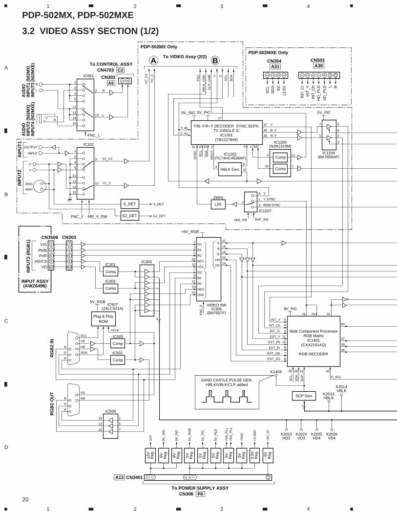
3.2 VIDEO ASSY SECTION (1/2)
PDP-502MX, PDP-502MXE
21
A
B
C
D
5 6 7 8
5 6 7 8
3
4
5
6
1
3
5
7
CN2203
2
3
4
5
6
CN2202
VD_PLD
HD_PLD
Peak ACL
124INT_RINT_R
INT_GINT_G
INT_BINT_B
EXT_REXT_R
EXT_GEXT_G
EXT_BEXT_B
133
139
126
136
141
101
103
98
IN Screen K2904(VD)
K2903(HD)
K2901(CLK)
AD OUT IP Process
NTSC 4:3 60 15.734k 40.28M Single (A) IP
PAL Wide 50 15.625k 53.63M Single (A) IP
PCXGA (60) ORG 60 48.36k 32.50M Dual (A/B) Through
P_ACL_SW
R (B)
G (B)
B (B)
R14
3 1 3
113
111
106 10
4
11 9 10
G B
R (A)
G (A)
B (A)
XCLK
1_2CLK
HD
XCLK
1_2CLK
HD
VD
CN2901
IC104
5 6
5V_PIC
Video DataROM
(24LC01B)
5V_PIC
+3.3AD
+5AD
+5V_PLL
IC140412
1314
SEL_Vout V_STATE
G-Out
B-Out
R-Out
12
11
6
1514
5432 10971
VD_FIL
HD_FIL
VD
_MA
SK
HD
_MA
SK
19
4HD/VD
NOISE GATEPULSE Gen.
IC2004(TC74VHC123AFT)
MMVMMV
HBLK_MAT/VBLK_MAT/CLP_MAT
HD3/VD3/HD4/VD4
SD
A
SC
L
Sync. ControlSync. Select
PLD
IC2005(PDY069)
142
137110
112
102
107
106
103
VD_FIL
VD_PLD
HD_PLD
V_STATE
VD
HD_FIL
AMP/AD/PLL
IC2402(CXA3506R)
K2015CLP
VD_PLDK2032
HD_PLDK2033
K24
17
K24
21
K24
19
K2030
K2029
K2012
XCLKK2012
1_2CLKK2012
HDK2012
VDK2012
K24
18
K24
22
K24
20
G/YK2004
K22
03
K22
04K
2201
K22
02
K2210K2211
K2209
K2212K2213
CLP1CLP2HBLKVBLK
CN2903
Sync. U-COMIC2201
(PD2060A9)
Sync. Sepa for Y/GIC2002
(M52346SP)
D/AIC2301
(CXA1875AM)
12V
+3.3AD
5V_PLD
K2021K2020
1008884 98 96 103
120
114
CLP
_AM
P
HD
_PLL
HO
LD_P
LL
ULK
_PLL
CLP
_AM
P
HD
_PLL
HO
LD_P
LL
ULK
_PLL
SDA
S2_DET
CLK
CLK
DATA
DA
TA
PLL_CE
PLL
_CE
SCL
SD
A
SC
L
18
FN
C_2
S_D
ET
R-Y
_LE
V
B-Y
_LE
V
MA
T_S
W
FN
C_0
FN
C_1
P_A
CL_
SW
KU
_SW
5V_PIC
19
31
16
4
2 22,23
HD
_u, V
D_u
4
4
CLK
DA_0_SV
128
131
132
3
VD
_SE
P
HD
_SE
P
+V
S
–HS
8
8
8
8
8
8
8
8
8
8
88
Reset
Input Freq. Det.
Gate
To
DIG
ITA
L V
IDE
O A
SS
Y
C
N34
03D
20T
o D
IGIT
AL
VID
EO
AS
SY
CN
3405
D22
To
U-C
OM
AS
SY
CN
3612
E24
To
U-C
OM
AS
SY
CN
2202
E23
A33
A35
A2
A1
8
9
10
11
CN2001
To
DIG
ITA
L V
IDE
O A
SS
Y
C
N34
02D
17
A3
R-Y
_LE
V
B-Y
_LE
V
PDP-502MX, PDP-502MXE
22
A
B
C
D
1 2 3 4
1 2 3 4
VC
_YV
3D_Y
in
3D_C
in
5VR
EG
.
LPF
(6.7
MH
z) LPF
(6.7
MH
z)
LPF
(6.
7MH
z)
IC80
3
Low
Lum
.C
NR
Cla
mp
Del
ay
250n
S
3.58
BP
FD
/AIC
703
(CX
A18
75A
M)
SC
L
SD
A 54
4.43
BP
F2
13
45
67
9
12
152 3 5 13 12
11 12 14 2 13
144115
13
4 14
13 1514
2 1 4 3 5
IC11
05
IC11
03
IC11
04
IC10
04S
in_C
3L_V
in
SCL
SDA
IC80
2IC
801
NT
SC
NT
SC
PA
L
PA
L
SE
CA
M
SE
CA
M_C
SIN
CSECAM
3.3V
RE
G.
IC11
01(U
PD
6408
2GF
-3B
A)
IC10
01(C
XD
2064
Q)
IS41
C16
256–
35K
IC11
06
LPF
(6.
7MH
z)
4M D
RA
M
SE
CA
MC
hrom
a T
rap
5VR
EG
.
YC
_C
1 47688 96 57
59
843D
_Y
3D_C
18 5
483
60
8
CS
I
AY
I
3DR
ST
CLP
O
AD
INA
YO
AC
O
9 7
8 5
1 21 4
37
2325
1726
FIN
MN
BPFSW
VSTRP1TRP2
VSBWNPMN
TRP0TRP1
TRP0TRP1
TRP2DLSW10
BPFSW
DLSWTRP2
TR
P2
VS/BW
NP
AC
I
RS
TB
5
IC10
03IC
1002
1 4
8 5
5V_3
D5V
_3D
AY
O
AC
O
5V_3
L
5V_3
L
3.3V
_3D
3.3V
_3D
5V_P
IC
5V_S
IG
TR
P2
FS
C
HB
LK_C
NR
CLP
_CN
R
Y C SC
L
SD
A
8V
3D Y
/C
3Lin
e Y
/C
MA (0:8)
MD (0:15)
To VIDEO Assy (1/2)
To VIDEO Assy (1/2)
3L_Y
3D_C
NTSC_CPAL_C
A
B
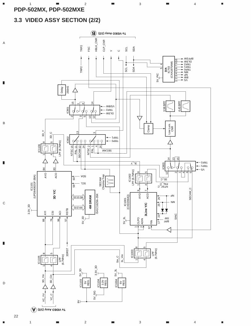
3.3 VIDEO ASSY SECTION (2/2)
PDP-502MX, PDP-502MXE
23
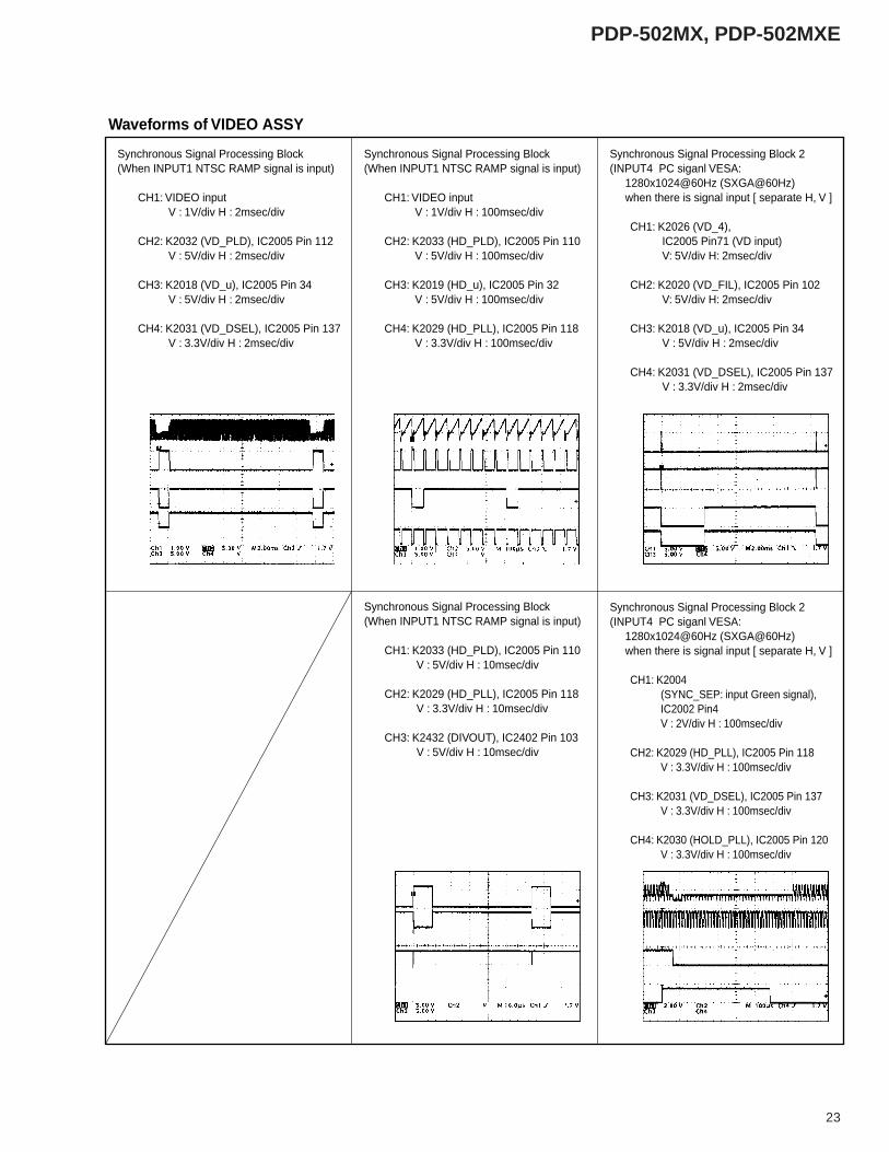
Waveforms of VIDEO ASSY
Synchronous Signal Processing Block(When INPUT1 NTSC RAMP signal is input)
CH1: VIDEO inputV : 1V/div H : 2msec/div
CH2: K2032 (VD_PLD), IC2005 Pin 112V : 5V/div H : 2msec/div
CH3: K2018 (VD_u), IC2005 Pin 34V : 5V/div H : 2msec/div
CH4: K2031 (VD_DSEL), IC2005 Pin 137V : 3.3V/div H : 2msec/div
Synchronous Signal Processing Block(When INPUT1 NTSC RAMP signal is input)
CH1: VIDEO inputV : 1V/div H : 100msec/div
CH2: K2033 (HD_PLD), IC2005 Pin 110V : 5V/div H : 100msec/div
CH3: K2019 (HD_u), IC2005 Pin 32V : 5V/div H : 100msec/div
CH4: K2029 (HD_PLL), IC2005 Pin 118V : 3.3V/div H : 100msec/div
Synchronous Signal Processing Block(When INPUT1 NTSC RAMP signal is input)
CH1: K2033 (HD_PLD), IC2005 Pin 110V : 5V/div H : 10msec/div
CH2: K2029 (HD_PLL), IC2005 Pin 118V : 3.3V/div H : 10msec/div
CH3: K2432 (DIVOUT), IC2402 Pin 103V : 5V/div H : 10msec/div
Synchronous Signal Processing Block 2 (INPUT4 PC siganl VESA: 1280x1024@60Hz (SXGA@60Hz) when there is signal input [ separate H, V ]
CH1: K2026 (VD_4), IC2005 Pin71 (VD input)V: 5V/div H: 2msec/div
CH2: K2020 (VD_FIL), IC2005 Pin 102V: 5V/div H: 2msec/div
CH3: K2018 (VD_u), IC2005 Pin 34V : 5V/div H : 2msec/div
CH4: K2031 (VD_DSEL), IC2005 Pin 137V : 3.3V/div H : 2msec/div
Synchronous Signal Processing Block 2 (INPUT4 PC siganl VESA: 1280x1024@60Hz (SXGA@60Hz) when there is signal input [ separate H, V ]
CH1: K2004(SYNC_SEP: input Green signal),IC2002 Pin4V : 2V/div H : 100msec/div
CH2: K2029 (HD_PLL), IC2005 Pin 118V : 3.3V/div H : 100msec/div
CH3: K2031 (VD_DSEL), IC2005 Pin 137V : 3.3V/div H : 100msec/div
CH4: K2030 (HOLD_PLL), IC2005 Pin 120V : 3.3V/div H : 100msec/div
PDP-502MX, PDP-502MXE
24
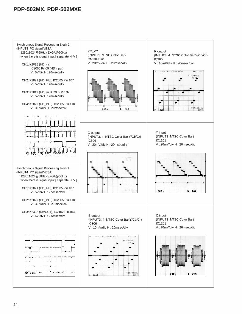
Synchronous Signal Processing Block 2 (INPUT4 PC siganl VESA: 1280x1024@60Hz (SXGA@60Hz) when there is signal input [ separate H, V ]
CH1: K2025 (HD_4), IC2005 Pin69 (HD input)V : 5V/div H : 20msec/div
CH2: K2021 (HD_FIL), IC2005 Pin 107V : 5V/div H : 20msec/div
CH3: K2019 (HD_u), IC2005 Pin 32V : 5V/div H : 20msec/div
CH4: K2029 (HD_PLL), IC2005 Pin 118V : 3.3V/div H : 20msec/div
Synchronous Signal Processing Block 2 (INPUT4 PC siganl VESA: 1280x1024@60Hz (SXGA@60Hz) when there is signal input [ separate H, V ]
CH1: K2021 (HD_FIL), IC2005 Pin 107V : 5V/div H : 2.5msec/div
CH2: K2029 (HD_PLL), IC2005 Pin 118V : 3.3V/div H : 2.5msec/div
CH3: K2432 (DIVOUT), IC2402 Pin 103V : 5V/div H : 2.5msec/div
YC_VY(INPUT1 NTSC Color Bar)CN104 Pin1V : 20mV/div H : 20msec/div
G output(INPUT3, 4 NTSC Color Bar Y/Cb/Cr)IC306V : 20mV/div H : 20msec/div
B output(INPUT3, 4 NTSC Color Bar Y/Cb/Cr)IC306V : 10mV/div H : 20msec/div
R output(INPUT3, 4 NTSC Color Bar Y/Cb/Cr)IC306V : 10mV/div H : 20msec/div
Y input(INPUT1 NTSC Color Bar)IC1201V : 20mV/div H : 20msec/div
C input(INPUT1 NTSC Color Bar)IC1201V : 20mV/div H : 20msec/div
PDP-502MX, PDP-502MXE
25
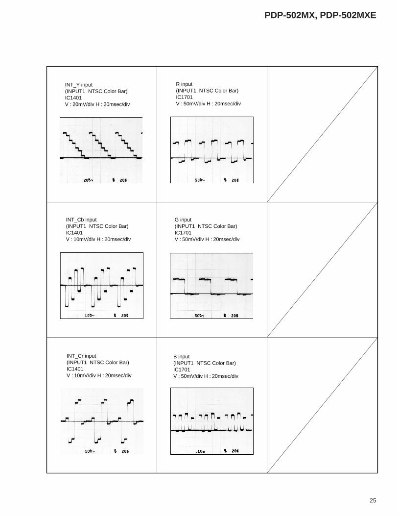
INT_Y input(INPUT1 NTSC Color Bar)IC1401V : 20mV/div H : 20msec/div
INT_Cb input(INPUT1 NTSC Color Bar)IC1401V : 10mV/div H : 20msec/div
INT_Cr input(INPUT1 NTSC Color Bar)IC1401V : 10mV/div H : 20msec/div
R input(INPUT1 NTSC Color Bar)IC1701V : 50mV/div H : 20msec/div
G input(INPUT1 NTSC Color Bar)IC1701V : 50mV/div H : 20msec/div
B input(INPUT1 NTSC Color Bar)IC1701V : 50mV/div H : 20msec/div
PDP-502MX, PDP-502MXE
26
A
B
C
D
1 2 3 4
1 2 3 4
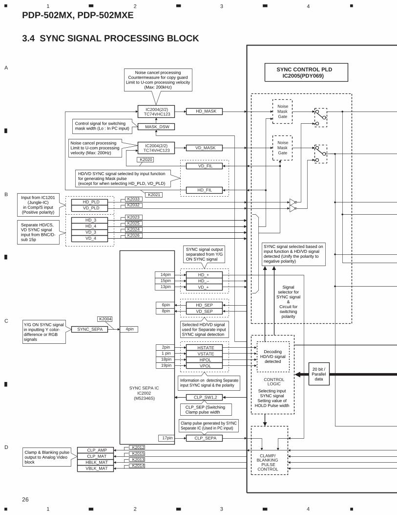
SYNC SEPA ICIC2002
(M52346S)
SYNC_SEPA
CONTROLLOGIC
CLP_SEPA
HSTATE
HPOLVSTATE
VPOL
CLAMP/BLANKING
PULSECONTROL
SYNC CONTROL PLDIC2005(PDY069)
MASK_DSW
CLP_SW1,2
HD_PLD
HD_3HD_4
VD_4VD_3
VD_PLD
IC2004(2/2)TC74VHC123
IC2004(2/2)TC74VHC123
CLP_AMPCLP_MAT
HBLK_MATVBLK_MAT
NoiseMaskGate
VD_FIL
VD_MASK
HD_FIL
HD_MASK
NoiseMaskGate
K2033
K2025K2023
K2032
K2026K2024
K2004
K2021
K2020
K2012K2015K2013K2014
13pin
8pin6pin
14pin HD_+
HD_SEP
VD_SEP
HD_–
VD_+
15pin
17pin
4pin
19pin18pin1 pin2pin
Input from IC1201 (Jungle-IC)
in Comp/S input (Positive polarity)
Separate HD/CS, VD SYNC signal input from BNC/D-sub 15p
Y/G ON SYNC signal in inputting Y color-difference or RGB signals
Clamp & Blanking pulse output to Analog Video block
Control signal for switching mask width (Lo : In PC input)
Noise cancel processing Limit to U-com processing velocity (Max: 200Hz)
HD/VD SYNC signal selected by input functionfor generating Mask pulse(except for when selecting HD_PLD, VD_PLD)
Noise cancel processing Countermeasure for copy guard
Limit to U-com processing velocity (Max: 200kHz)
SYNC signal output separated from Y/G ON SYNC signal
Selected HD/VD signal used for Separate input SYNC signal detection
Information on detecting Separate input SYNC signal & the polarity
CLP_SEP (Switching Clamp pulse width
Clamp pulse generated by SYNC Separate IC (Used in PC input)
SYNC signal selected based on input function & HD/VD signal detected (Unify the polarity to negative polarity)
Signal selector for
SYNC signal &
Circuit for switching polarity
Decoding HD/VD signal
detected
Selecting input SYNC signal
Setting value of HOLD Pulse width
20 bit / Parallel
data
3.4 SYNC SIGNAL PROCESSING BLOCK
PDP-502MX, PDP-502MXE
27
A
B
C
D
5 6 7 8
5 6 7 8
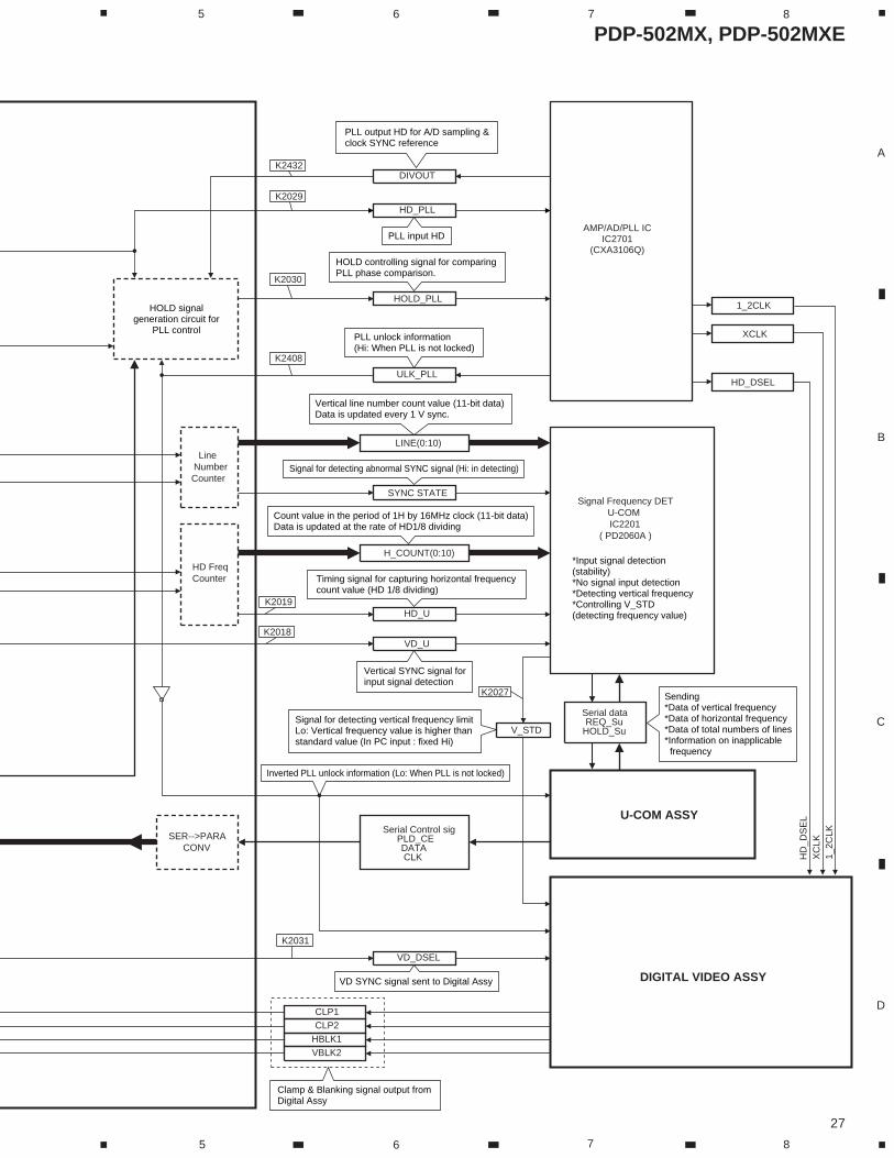
Signal Frequency DETU-COMIC2201
( PD2060A )
AMP/AD/PLL ICIC2701
(CXA3106Q)
HD_U
VD_U
HD_PLL
DIGITAL VIDEO ASSY
CLP1CLP2
HBLK1VBLK2
ULK_PLL
Serial Control sigPLD_CEDATACLK
VD_DSEL
SER-->PARACONV
HOLD_PLL
DIVOUT
U-COM ASSY
V_STD
Serial dataREQ_Su
HOLD_Su
PLL input HD
HD FreqCounter
LineNumberCounter
SYNC STATE
K2030
K2019
K2029
K2018
K2031
K2408
K2432
K2027
HD_DSEL
XCLK
1_2CLK
HD
_DS
EL
XC
LK1_
2CLK
H_COUNT(0:10)
LINE(0:10)
HOLD signal generation circuit for
PLL control
Inverted PLL unlock information (Lo: When PLL is not locked)
Clamp & Blanking signal output from Digital Assy
PLL output HD for A/D sampling &clock SYNC reference
HOLD controlling signal for comparing PLL phase comparison.
PLL unlock information (Hi: When PLL is not locked)
Vertical line number count value (11-bit data) Data is updated every 1 V sync.
Signal for detecting abnormal SYNC signal (Hi: in detecting)
Count value in the period of 1H by 16MHz clock (11-bit data) Data is updated at the rate of HD1/8 dividing
Timing signal for capturing horizontal frequency count value (HD 1/8 dividing)
Vertical SYNC signal for input signal detection
Signal for detecting vertical frequency limitLo: Vertical frequency value is higher than standard value (In PC input : fixed Hi)
VD SYNC signal sent to Digital Assy
*Input signal detection (stability) *No signal input detection *Detecting vertical frequency *Controlling V_STD (detecting frequency value)
Sending*Data of vertical frequency*Data of horizontal frequency *Data of total numbers of lines*Information on inapplicable frequency
PDP-502MX, PDP-502MXE
28
A
B
C
D
1 2 3 4
1 2 3 4
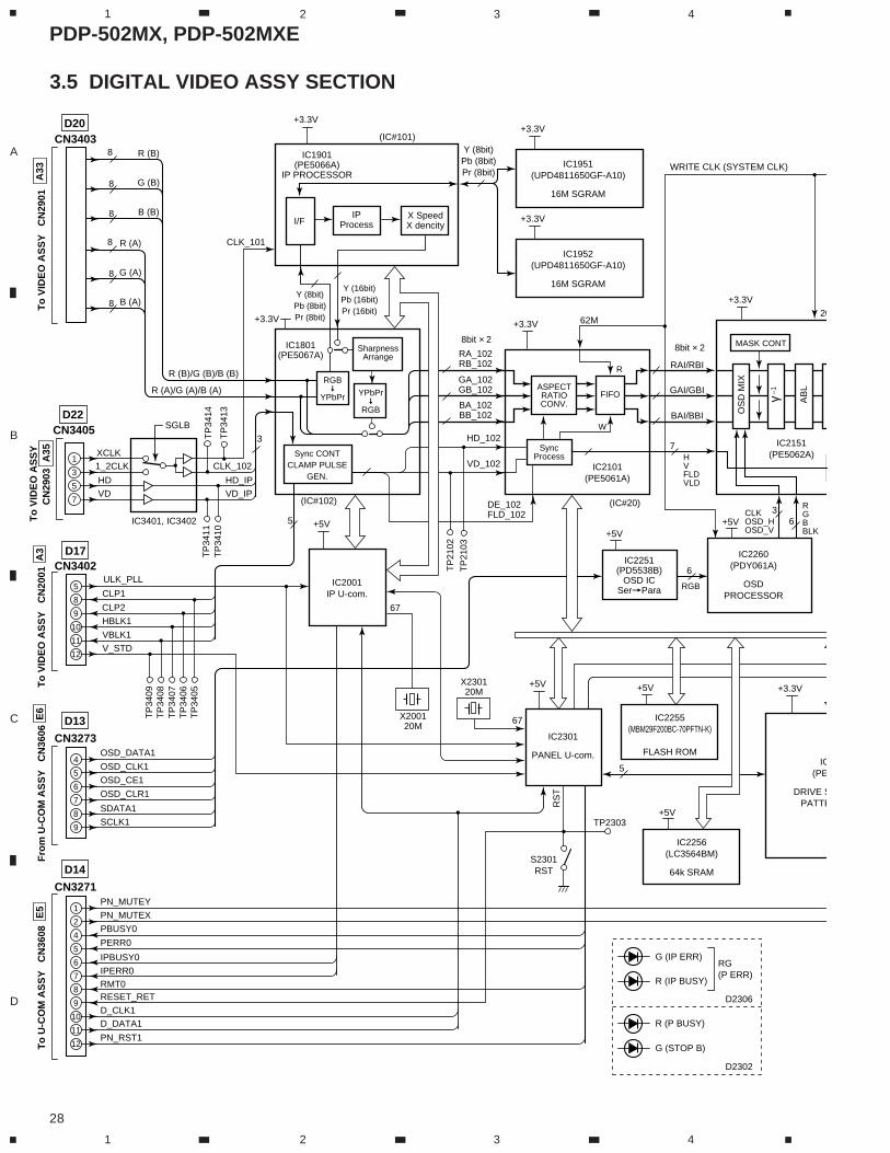
3.5 DIGITAL VIDEO ASSY SECTION
R (A)/G (A)/B (A)
VD_102
DE_102FLD_102
HD_102
RA_102RB_102
8bit × 28bit × 2
GA_102GB_102
BA_102BB_102
R (B)/G (B)/B (B)
OSD_DATA1
OSD_CLK1
OSD_CE1
OSD_CLR1
SDATA1
SCLK1
PN_MUTEY
PN_MUTEX
PBUSY0
PERR0
IPBUSY0
IPERR0RMT0RESET_RET
D_CLK1D_DATA1
PN_RST1
IC1801(PE5067A)
Sync CONTCLAMP PULSE
GEN.
RGB≠
YPbPr
SharpnessArrange
IC2001IP U-com.
IC3401, IC3402
(IC#101)
(IC#102) (IC#20)
IC1901(PE5066A)
IP PROCESSOR
I/FIP
ProcessX SpeedX dencity
IC1951(UPD4811650GF-A10)
16M SGRAM
+3.3V
CLK_101
CLK_102 IC2101(PE5061A)
IC2260(PDY061A)
OSDPROCESSOR
+3.3V 62M
+3.3V
20
+3.3V
+5V
67
67
ULK_PLL
+3.3V
Y (8bit)Pb (8bit)Pr (8bit)
Y (8bit)Pb (8bit)Pr (8bit)
Y (16bit)Pb (16bit)Pr (16bit)
+3.3V
IC1952(UPD4811650GF-A10)
16M SGRAM
+3.3V
5
7
R (B)
G (B)
B (B)
8
8
8
CN3403
3 IC2151(PE5062A)
IC(PE
DRIVE SPATTE
8
5
9
10
11
12
CN3402D17
CN3273
D13
D20
TP
3408
TP
3409
TP
3407
TP
3406
TP
3405
VBLK1
V_STD
HBLK1
CLP2
CLP1
TP
2102
TP
2103
IC2301
PANEL U-com.
S2301RST
TP2303
D2306
D2302
R (IP BUSY)
G (IP ERR)RG(P ERR)
RS
T
+5V
X200120M
X230120M +5V
5
4
6
7
8
9
CN3271
D14
2
1
4
5
6
7
8
9
10
11
12
RAI/RBI
WRITE CLK (SYSTEM CLK)
GAI/GBI
BAI/BBI
HVFLDVLD
CLKOSD_HOSD_V
RGBBLK
RGB
6
5
63
IC2251(PD5538B)
OSD ICSer=Para
IC2255(MBM29F200BC-70PFTN-K)
FLASH ROM
+5V
IC2256(LC3564BM)
64k SRAM
To
U-C
OM
AS
SY
C
N36
08E
5F
rom
U-C
OM
AS
SY
C
N36
06E
6T
o V
IDE
O A
SS
Y
CN
2001
A3
To
VID
EO
AS
SY
C
N29
01A
33
R (A)
G (A)
B (A)
8
8
8
+5V+5V
1
3
5
7
TP
3411
TP
3410
TP
3414
TP
3413
1_2CLK
VDHD
VD_IPHD_IP
XCLK
SGLBCN3405D22
To
VID
EO
AS
SY
CN
2903
A35
OS
D M
IX
AB
L
γ –1
YPbPr≠
RGB
ASPECTRATIOCONV.
W
R
SyncProcess
MASK CONT
FIFO
R (P BUSY)
G (STOP B)
PDP-502MX, PDP-502MXE
29
A
B
C
D
5 6 7 8
5 6 7 8
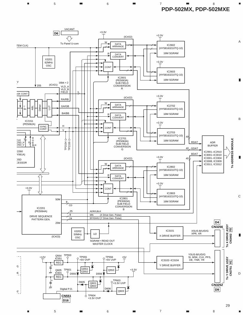
16bit × 2(IC#21)
C2260Y061A)
OSDCESSOR
V
205
+3.3V
IC2151(PE5062A)
IC2201(PE5064A)
DRIVE SEQUENCEPATTERN GEN.
IC2601(PE5063A)SUB FIELD
CONVERSIONR
ADRBUFFER
IC2901–IC2910IC3001–IC3010IC3301–IC3304IC3308, IC3309IC3311, IC3312
IC2701(PE5063A)SUB FIELD
CONVERSIONG
R
WDATA
ARRANGE
DATACONVERT
CONT
(IC#22)
IC2801(PE5063A)SUB FIELD
CONVERSIONB
Q605IC601
Q554IC551
IC2602(HY58163210TQ-10)
16M SGRAM
IC2603(HY58163210TQ-10)
16M SGRAM
IC2702(HY58163210TQ-10)
16M SGRAM
IC2703(HY58163210TQ-10)
16M SGRAM
IC2802(HY58163210TQ-10)
16M SGRAM
IC2803(HY58163210TQ-10)
16M SGRAM
+3.3V
R
W
+3.3V
+3.3V
+3.3V
+3.3V
+3.3V
40
40
40
RDAT
GDAT
BDAT
+3.3V
CN3252
CN3256
D9
D4
TP
2154
TP
2155
06
02
R)
TEM CLK)
VACANT
To Panel U-com
VLD_AVLD_BFIELD
RA/RB
GA/GB
BA/BB
H
V
CLKOSD_HOSD_V
RGBBLK
3
6
8CD
50M
25M
3
IC3101
X DRIVE BUFFER
XSUS-B/U/D/GXPR, XR
IC3102–IC3104
Y DRIVE BUFFER
X320250MHzOSC
SGRAM • READ OUT MASTER CLOCK
X320162MHzOSC
1/2
To
X D
RIV
E A
SS
Y
CN
3402
F9
To
Y D
RIV
E A
SS
Y
CN
3751
H1
To
AD
DR
ES
S M
OD
UL
E
+5V
+3.3V
CN551D16
825 ADR/LBLK
MN (X Drive Gen. Pulse)EF/GH/IJ (Y Drive Gen. Pulse)24
TP601
TP553
D555
Digital P.D.
D605
Q551Q552
TP555+5V OVP
TP604+3.3V OVP
REG
REG
AB
L
γ –1
Dith
er
LUT
DATAARRANGE
DATACONVERT
CONT
SYNCCONT
ASK CONT
(IC#22)
R
WDATA
ARRANGE
DATACONVERT
CONT
(IC#22)
(IC#23)
YSUS-B/U/D/GSI, MSK, CLK, PFS, OE, YNR, YR
D6
+
+
+12V
D556
Q553
TP556+5V UVP
Q601Q602
D606
TP603+3.3V UVP
Q603
PDP-502MX, PDP-502MXE
30
Waveforms of X DIGITAL VIDEO ASSY
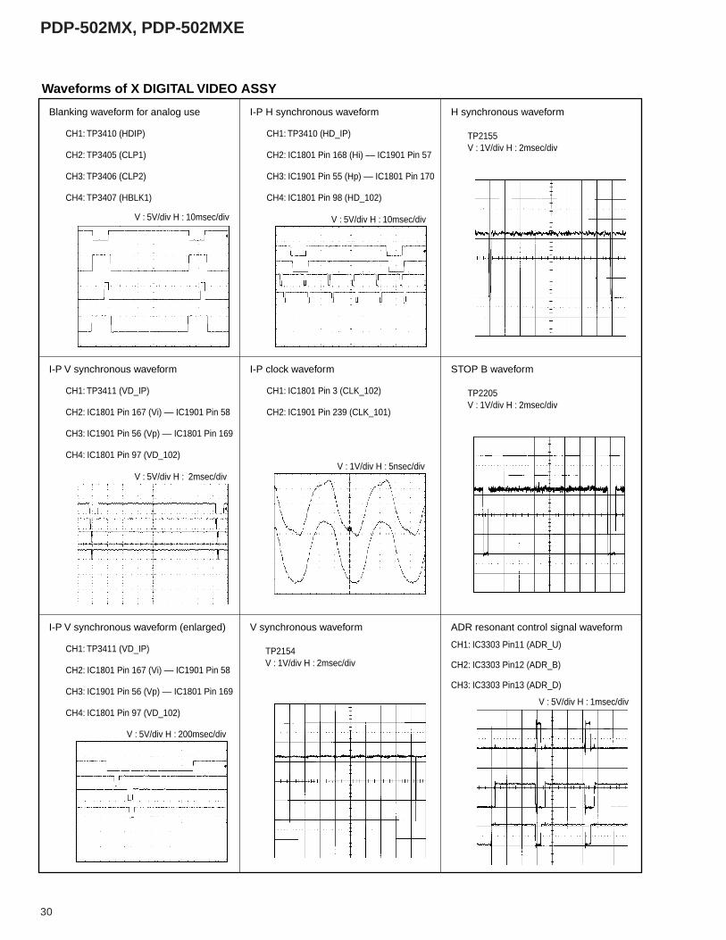
Blanking waveform for analog use
CH1: TP3410 (HDIP)
CH2: TP3405 (CLP1)
CH3: TP3406 (CLP2)
CH4: TP3407 (HBLK1)
I-P V synchronous waveform
CH1: TP3411 (VD_IP)
CH2: IC1801 Pin 167 (Vi) –– IC1901 Pin 58
CH3: IC1901 Pin 56 (Vp) –– IC1801 Pin 169
CH4: IC1801 Pin 97 (VD_102)
I-P V synchronous waveform (enlarged)
CH1: TP3411 (VD_IP)
CH2: IC1801 Pin 167 (Vi) –– IC1901 Pin 58
CH3: IC1901 Pin 56 (Vp) –– IC1801 Pin 169
CH4: IC1801 Pin 97 (VD_102)
I-P H synchronous waveform
CH1: TP3410 (HD_IP)
CH2: IC1801 Pin 168 (Hi) –– IC1901 Pin 57
CH3: IC1901 Pin 55 (Hp) –– IC1801 Pin 170
CH4: IC1801 Pin 98 (HD_102)
I-P clock waveform
CH1: IC1801 Pin 3 (CLK_102)
CH2: IC1901 Pin 239 (CLK_101)
V synchronous waveform
TP2154V : 1V/div H : 2msec/div
H synchronous waveform
TP2155V : 1V/div H : 2msec/div
STOP B waveform
TP2205V : 1V/div H : 2msec/div
ADR resonant control signal waveform
CH1: IC3303 Pin11 (ADR_U)
CH2: IC3303 Pin12 (ADR_B)
CH3: IC3303 Pin13 (ADR_D)
V : 5V/div H : 10msec/div
V : 5V/div H : 2msec/div
V : 5V/div H : 200msec/div
V : 5V/div H : 10msec/div
V : 1V/div H : 5nsec/div
V : 5V/div H : 1msec/div
PDP-502MX, PDP-502MXE
31
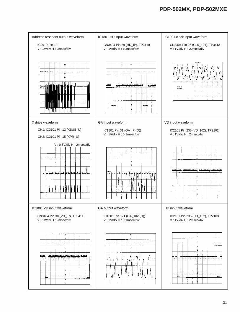
Address resonant output waveform
IC2910 Pin 13V : 1V/div H : 2msec/div
X drive waveform
CH1: IC3101 Pin 12 (XSUS_U)
CH2: IC3101 Pin 15 (XPR_U)
IC1801 VD input waveform
CN3404 Pin 30 (VD_IP), TP3411V : 1V/div H : 2msec/div
IC1801 HD input waveform
CN3404 Pin 29 (HD_IP), TP3410V : 1V/div H : 10msec/div
GA input waveform
IC1801 Pin 31 (GA_IP (O))V : 1V/div H : 0.1msec/div
GA output waveform
IC1801 Pin 121 (GA_102 (O))V : 1V/div H : 0.1msec/div
IC1901 clock input waveform
CN3404 Pin 26 (CLK_101), TP3413V : 1V/div H : 20nsec/div
VD input waveform
IC2101 Pin 236 (VD_102), TP2102V : 1V/div H : 2msec/div
HD input waveform
IC2101 Pin 235 (HD_102), TP2103V : 1V/div H : 2msec/div
V : 0.5V/div H : 2msec/div
PDP-502MX, PDP-502MXE
32
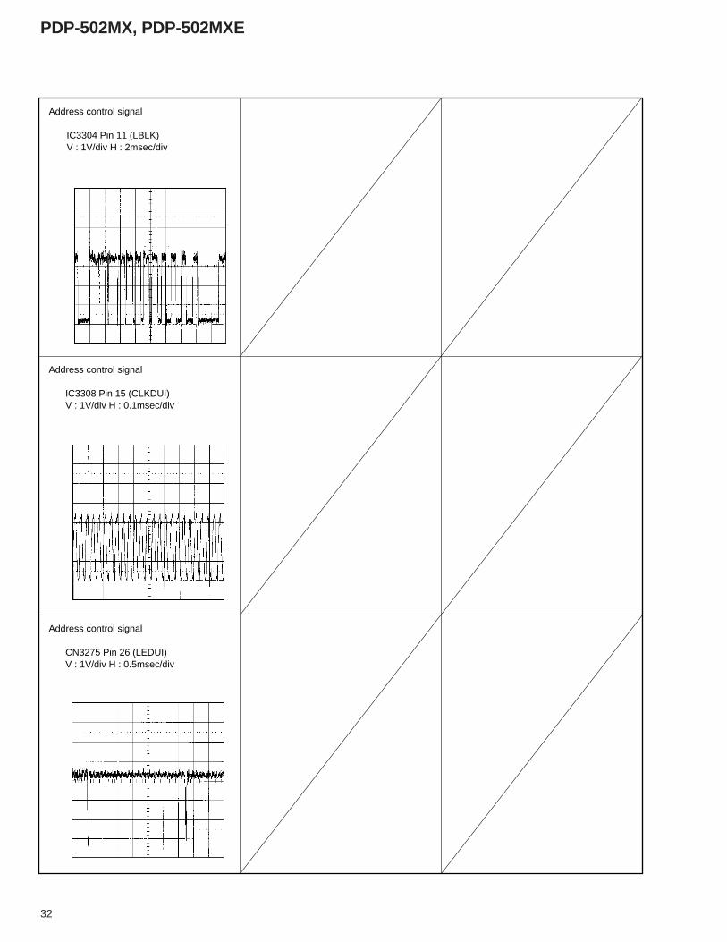
Address control signal
IC3304 Pin 11 (LBLK)V : 1V/div H : 2msec/div
Address control signal
IC3308 Pin 15 (CLKDUI)V : 1V/div H : 0.1msec/div
Address control signal
CN3275 Pin 26 (LEDUI)V : 1V/div H : 0.5msec/div
PDP-502MX, PDP-502MXE
33
A
B
C
D
1 2 3 4
1 2 3 4
XS
US
-BR
3435
IC34
04
IC34
04R
3424
IC34
03(T
C74
AC
11F
)
PD
P P
uls
e M
od
ule
IC34
02(S
TK
795-
450)
+RE
SE
T B
LO
CK
LO
GIC
BL
OC
K
IC34
08(T
C74
AC
08F
)
IC34
03
R34
06
R34
38
+5V
Q34
06
Q34
05
D34
08
K34
10P
.D. (
X.C
.P)
C34
04
Q34
04
Q34
01–Q
3403
11
XS
US
-VX
SU
S-D
XS
US
-GX
PR
-U
9 7
1 3 5
5
6 638
3 9 2 1 5 44 11 10
SU
S-B
1 1312
SUS-DK3412
SUS-GK3414 SUS-U
K3411
SUS-BK3413
PR-UK3409
2
+12
V
75 3
+5V
+5V
VS
US
(175
V)
1
+12
V
XP
D
3 6 7 5
VS
US
(175
V)
1
SU
SG
ND
2 3 4
PD
DE
T.
12V
O. C
DE
T.
SU
S-U
212629
40
20 18 14161
175V
175V
0V
VS
US
(175
V)
P-S
US
(X
)
SU
SG
ND
SU
SG
ND
SU
SG
ND
To
PA
NE
L
24V
SU
S/2
VS
US
SU
SO
UT
SUSG
ND
SU
S-D
VD
D
VC
C
32S
US
-G
VS
US
SU
S-G
SU
S-U
SU
S-B
SU
S-D
175V 0V
R34
10R
3411
D34
03
D3402
t
tX
-PS
US
SU
SG
ND
VS
US
RP
-U
F6
F5
F7
D4 From DIGITAL VIDEO Assy E17 From U-COM AssyE16 From U-COM Assy
PD
P P
uls
e M
od
ule
IC34
05(S
TK
795-
450)
SU
S-B
SU
S-U
212629
40
20 18 14161
VS
US
(175
V)
SU
SG
ND
SU
SG
ND
24V
SU
S/2
VS
US
SU
SO
UT
SUSG
ND
SU
S-D
VD
D
VC
C
32S
US
-G
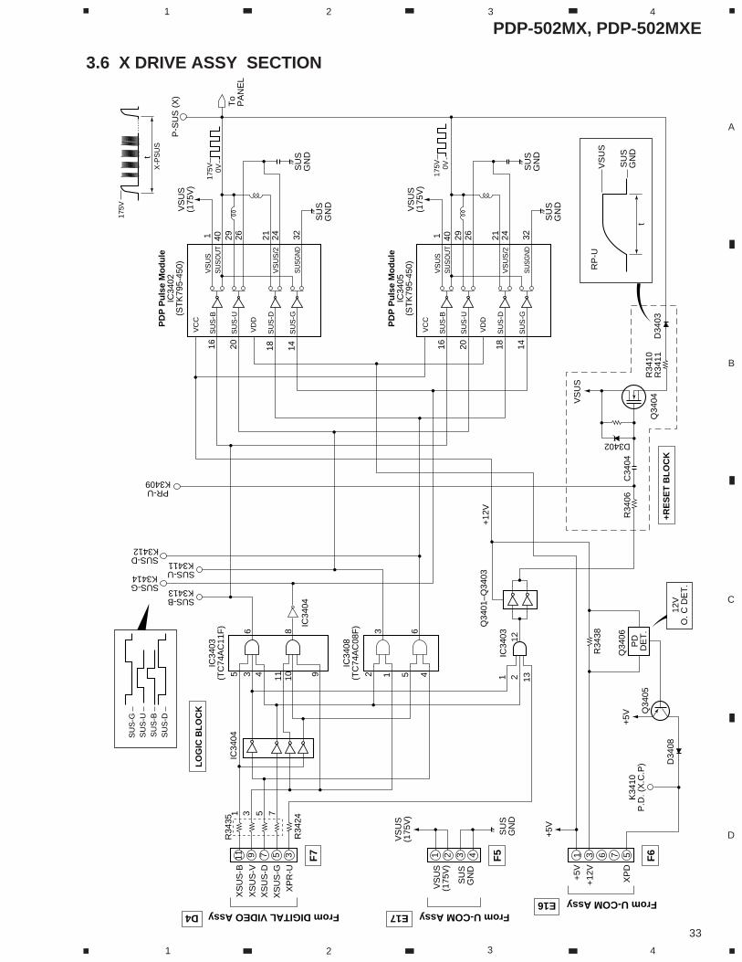
3.6 X DRIVE ASSY SECTION
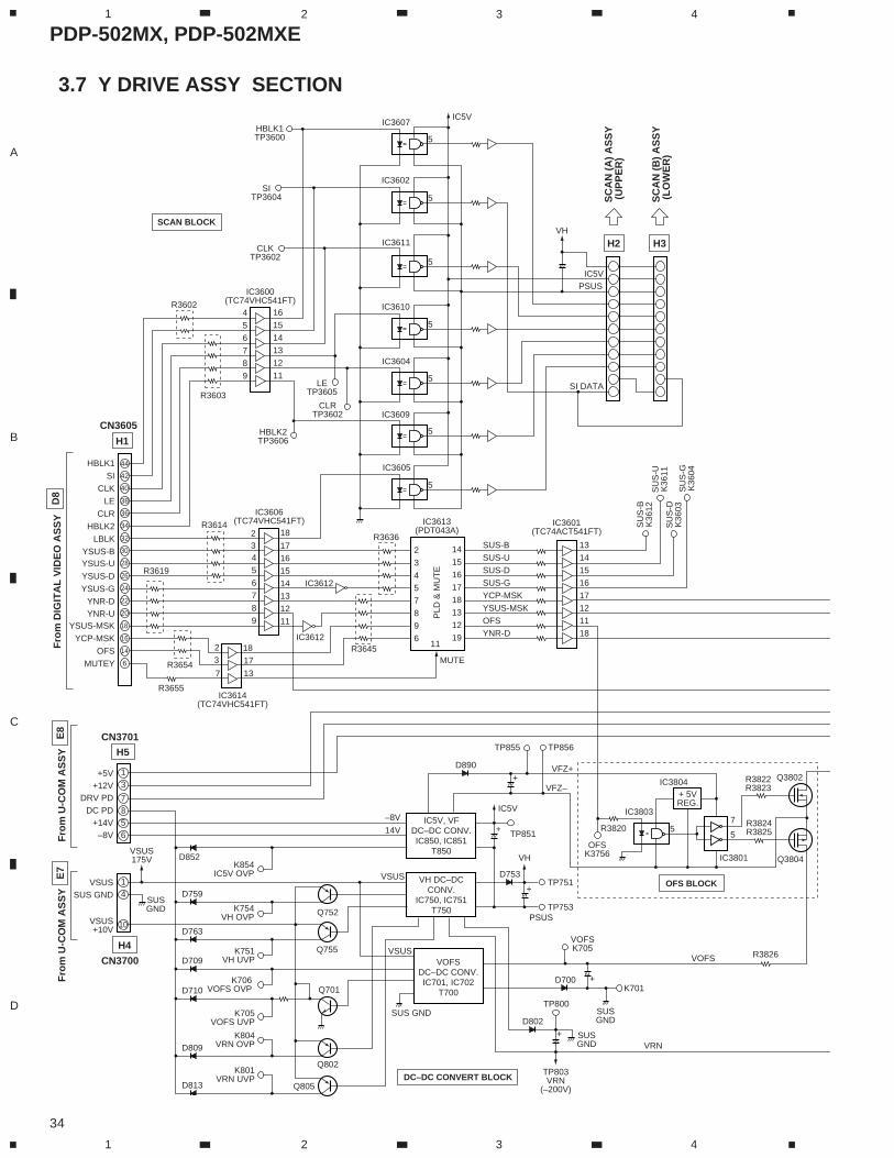
PDP-502MX, PDP-502MXE
34
A
B
C
D
1 2 3 4
1 2 3 4
IC3612
IC3612
R3636
R3645
7856
31
28
26
24
22
20
36
34
38
40
42
44
32
30
18
16
14
6
41
10
SUS GND
D763
D710
D709
D759
D852
14V
–8V
D890
D700
Q752
Q755
D813
D809
Q802
Q805
Q701
H2
SC
AN
(A
) A
SS
Y (
UP
PE
R)
SC
AN
(B
) A
SS
Y (
LO
WE
R)
D8
Fro
m D
IGIT
AL
VID
EO
AS
SY
H1
H3
YNR-D
MUTE
OFSYSUS-MSKYCP-MSKSUS-GSUS-DSUS-USUS-B
PLD
& M
UT
E
YSUS-BLBLK
HBLK2CLR
YNR-DYSUS-GYSUS-DYSUS-U
YNR-U
MUTEY
+5V+12V
DRV PDDC PD
+14V
VSUSSUS GND
VSUS+10V
–8V
OFSYCP-MSK
YSUS-MSK
LECLK
SIHBLK1
1911
12131817161514
1811121716151413
11
7
121314151617
17
13
18
1869875432
987654
987654
R3614
R3602
R3603
R3619
R3654
R3655
SU
S-D
K36
03
IC3601(TC74ACT541FT)
IC3613(PDT043A)
3
3
2
2
IC3607
5
SCAN BLOCK
OFS BLOCK
DC–DC CONVERT BLOCK
SU
S-G
K36
04
SU
S-U
K36
11
SU
S-B
K36
12
TP851
TP855 TP856
TP753PSUS
K701
TP751+
+
HBLK1TP3600
SITP3604
CLKTP3602
LETP3605
CLRTP3602
HBLK2TP3606
IC3600(TC74VHC541FT)
IC3606(TC74VHC541FT)
IC3614(TC74VHC541FT)
12
11
13141516
IC3602
5
IC3611
5
IC3610
5
IC3604
5SI DATA
PSUSIC5V
IC3609
5
IC3605
VH DC–DCCONV.
IC750, IC751T750
K854IC5V OVP
K754VH OVP
K751VH UVP
K706VOFS OVP
K705VOFS UVP
K804VRN OVP
K801VRN UVP
VOFSK705
OFSK3756
IC5V, VFDC–DC CONV.IC850, IC851
T850
VOFSDC–DC CONV.IC701, IC702
T700
5
SUSGND
SUSGND
VSUS
VSUS
SUSGND
D753
+
IC5V
VHVSUS175V
D802
TP803VRN
(–200V)
TP800
+
+
+ 5VREG.
IC3803
IC3801
IC3804
55
7
Q3802R3822R3823
R3824R3825
R3826VOFS
VFZ+
VFZ–
VRN
R3820
Q3804
VH
E8
Fro
m U
-CO
M A
SS
Y
CN3701
CN3605
CN3700
H5
E7
Fro
m U
-CO
M A
SS
Y
H4
IC5V
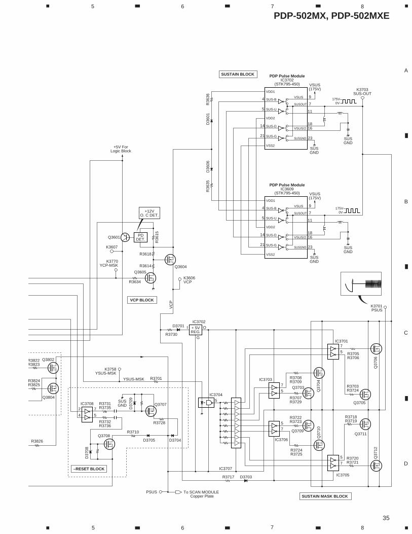
3.7 Y DRIVE ASSY SECTION
PDP-502MX, PDP-502MXE
35
A
B
C
D
5 6 7 8
5 6 7 8
To SCAN MODULE Copper Plate
D3701IC3702
IC3704
IC3703
IC3706
IC3705
IC3701
IC3707
R3701YSUS-MSK
R3730
R3728
D3705 D3704
Q3601
Q3605Q3604
R3634
R3614
R3618
R36
36
PDP Pulse ModuleIC3702
(STK795-450)
SUSTAIN BLOCK
D36
01R
3635
D36
06
SUS-B
SUS-U
18
11
75
14
21
4 9 175V0V
VSUS(175V) K3703
SUS-OUT
SUSGND
SUSGND
16VSUS/2
VSUS
SUSOUT
SUSGND
SUS-D
VDD2
VDD1
VSS2
23SUS-G
PDP Pulse ModuleIC3609
(STK795-450)
SUS-B
SUS-U
18
11
75
14
21
4 9
VSUS(175V)
SUSGND
SUSGND
16VSUS/2
VSUS
SUSOUT
SUSGND
SUS-D
VDD2
VDD1
VSS2
23SUS-G
175V0V
5
VCP BLOCK
–RESET BLOCK
SUSTAIN MASK BLOCK
K3758YSUS-MSK
K3701PSUS
K3606VCP
VC
P
SUSGND
+5V ForLogic Block
R36
15PDDET.
7
5
R3732R3736
R3731R3735
IC37082
4
+ 5VREG.
O
G
I
D3703R3717
Q3802R3822R3823
R3824R3825
R3826
Q3804
Q3708R3710
Q3707
Q3709
Q3703
R3707R3729
R3708R3709
R3722R3723
R3724R3725
R3703R3724
R3705R3706
R3718R3719
R3720R3721
Q37
10Q
3704
Q3705
5
7
7
5
7
5
7
5
Q3711
Q37
12Q
3706
K3770YCP-MSK
K3607
D37
09
D37
08
+12VO. C DET.
PSUS
PDP-502MX, PDP-502MXE
36
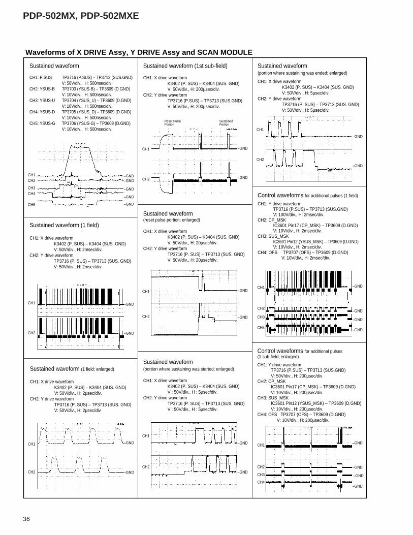
Control waveforms for additional pulses(1 sub-field; enlarged)
CH1: Y drive waveformTP3716 (P.SUS) – TP3713 (SUS.GND)V: 50V/div., H: 200µsec/div.
CH2: CP_MSKIC3601 Pin17 (CP_MSK) – TP3609 (D.GND)V: 10V/div., H: 200µsec/div.
CH3: SUS_MSKIC3601 Pin12 (YSUS_MSK) – TP3609 (D.GND)V: 10V/div., H: 200µsec/div.
CH4: OFS TP3707 (OFS) – TP3609 (D.GND) V: 10V/div., H: 200µsec/div.
–GND–GND
–GND
–GND
–GND
–GND
–GND
–GND
–GND
–GND
–GND
–GND
–GND
–GND
–GND
–GND
–GND
–GND
–GND
–GND
–GND
–GND
–GND
–GND
–GNDCH5
CH4CH3
CH2CH1
CH2
CH1
CH2
CH2
CH1
CH2
CH1
CH1CH1
CH2
CH3
CH4
CH1
CH2
CH3
CH4
CH2
CH1
CH2
CH1
Sustained waveform (1 field; enlarged)
CH1: X drive waveformK3402 (P. SUS) – K3404 (SUS. GND)V: 50V/div., H: 2µsec/div.
CH2: Y drive waveformTP3716 (P. SUS) – TP3713 (SUS. GND)V: 50V/div., H: 2µsec/div
Sustained waveform (1 field)
CH1: X drive waveform K3402 (P. SUS) – K3404 (SUS. GND)V: 50V/div., H: 2msec/div.
CH2: Y drive waveform TP3716 (P. SUS) – TP3713 (SUS. GND)V: 50V/div., H: 2msec/div.
Sustained waveform
CH1: P.SUS TP3716 (P.SUS) – TP3713 (SUS.GND)V: 50V/div., H: 500nsec/div.
CH2: YSUS-B TP3703 (YSUS-B) – TP3609 (D.GND)V: 10V/div., H: 500nsec/div.
CH3: YSUS-U TP3704 (YSUS_U) – TP3609 (D.GND)V: 10V/div., H: 500nsec/div.
CH4: YSUS-D TP3705 (YSUS_D) – TP3609 (D.GND)V: 10V/div., H: 500nsec/div.
CH5: YSUS-G TP3706 (YSUS-G) – TP3609 (D.GND)V: 10V/div., H: 500nsec/div.
Sustained waveform (1st sub-field)
CH1: X drive waveformK3402 (P. SUS) – K3404 (SUS. GND)V: 50V/div., H: 200µsec/div.
CH2: Y drive waveformTP3716 (P.SUS) – TP3713 (SUS.GND)V: 50V/div., H: 200µsec/div.
Sustained waveform (portion where sustaining was ended; enlarged)
CH1: X drive waveformK3402 (P. SUS) – K3404 (SUS. GND)V: 50V/div., H: 5µsec/div.
CH2: Y drive waveformTP3716 (P. SUS) – TP3713 (SUS. GND)V: 50V/div., H: 5µsec/div.
Sustained waveform(reset pulse portion; enlarged)
CH1: X drive waveformK3402 (P. SUS) – K3404 (SUS. GND)V: 50V/div., H: 20µsec/div.
CH2: Y drive waveformTP3716 (P. SUS) – TP3713 (SUS. GND)V: 50V/div., H: 20µsec/div.
Sustained waveform (portion where sustaining was started; enlarged)
CH1: X drive waveformK3402 (P. SUS) – K3404 (SUS. GND)V : 50V/div., H : 5µsec/div.
CH2: Y drive waveformTP3716 (P. SUS) – TP3713 (SUS. GND)V : 50V/div., H : 5µsec/div.
Control waveforms for additional pulses (1 field)
CH1: Y drive waveformTP3716 (P.SUS) – TP3713 (SUS.GND)V: 100V/div., H: 2msec/div.
CH2: CP_MSKIC3601 Pin17 (CP_MSK) – TP3609 (D.GND)V: 10V/div., H: 2msec/div.
CH3: SUS_MSKIC3601 Pin12 (YSUS_MSK) – TP3609 (D.GND)V: 10V/div., H: 2msec/div.
CH4: OFS TP3707 (OFS) – TP3609 (D.GND) V: 10V/div., H: 2msec/div.
Waveforms of X DRIVE Assy, Y DRIVE Assy and SCAN MODULE
Reset PulsePortion
SustainedPortion
PDP-502MX, PDP-502MXE
37
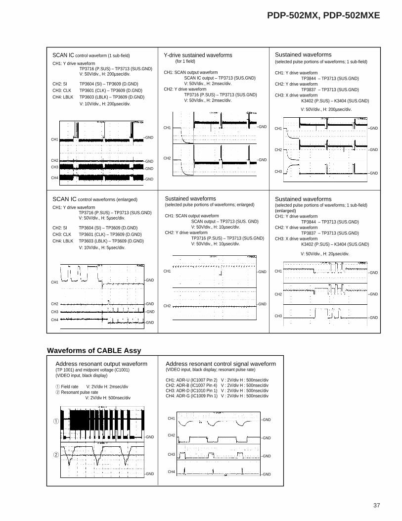
SCAN IC control waveform (1 sub-field)
CH1: Y drive waveformTP3716 (P.SUS) – TP3713 (SUS.GND)V: 50V/div., H: 200µsec/div.
CH2: SI TP3604 (SI) – TP3609 (D.GND)CH3: CLK TP3601 (CLK) – TP3609 (D.GND)CH4: LBLK TP3603 (LBLK) – TP3609 (D.GND)
–GND
–GND
–GND
–GND
–GND–GND
–GND
–GND
–GND
–GND
–GND
–GND
CH4
CH3
CH2
CH1
CH2
CH1
CH2
CH1
CH4
CH3
CH2
CH1
Y-drive sustained waveforms (for 1 field)
CH1: SCAN output waveformSCAN IC output – TP3713 (SUS.GND)V: 50V/div., H: 2msec/div.
CH2: Y drive waveformTP3716 (P.SUS) – TP3713 (SUS.GND)V: 50V/div., H: 2msec/div.
Sustained waveforms(selected pulse portions of waveforms; enlarged)
CH1: SCAN output waveformSCAN output – TP3713 (SUS. GND)V: 50V/div., H: 10µsec/div.
CH2: Y drive waveformTP3716 (P.SUS) – TP3713 (SUS.GND)V: 50V/div., H: 10µsec/div.
SCAN IC control waveforms (enlarged)
CH1: Y drive waveformTP3716 (P.SUS) – TP3713 (SUS.GND)V: 50V/div., H: 5µsec/div.
CH2: SI TP3604 (SI) – TP3609 (D.GND)CH3: CLK TP3601 (CLK) – TP3609 (D.GND)CH4: LBLK TP3603 (LBLK) – TP3609 (D.GND)
V: 10V/div., H: 200µsec/div.
V: 10V/div., H: 5µsec/div.
–GND
–GND
–GND
CH2
CH3
CH1
Sustained waveforms (selected pulse portions of waveforms; 1 sub-field)
CH1: Y drive waveformTP3844 – TP3713 (SUS.GND)
CH2: Y drive waveformTP3837 – TP3713 (SUS.GND)
CH3: X drive waveformK3402 (P.SUS) – K3404 (SUS.GND)
V: 50V/div., H: 200µsec/div.
–GND
–GND
–GND
CH2
CH3
CH1
Sustained waveforms (selected pulse portions of waveforms; 1 sub-field)(enlarged)CH1: Y drive waveform
TP3844 – TP3713 (SUS.GND)CH2: Y drive waveform
TP3837 – TP3713 (SUS.GND)CH3: X drive waveform
K3402 (P.SUS) – K3404 (SUS.GND)
V: 50V/div., H: 20µsec/div.
–GND
–GND
–GND
–GND
–GND
–GND
CH4
CH3
CH2
CH1
Waveforms of CABLE Assy
Address resonant control signal waveform(VIDEO input, black display; resonant pulse rate)
CH1: ADR-U (IC1007 Pin 2) V : 2V/div H : 500nsec/divCH2: ADR-B (IC1007 Pin 4) V : 2V/div H : 500nsec/divCH3: ADR-D (IC1010 Pin 1) V : 2V/div H : 500nsec/divCH4: ADR-G (IC1009 Pin 1) V : 2V/div H : 500nsec/div
Address resonant output waveform (TP 1001) and midpoint voltage (C1001)(VIDEO input, black display)
1 Field rate V: 2V/div H: 2msec/div2 Resonant pulse rate
V: 2V/div H: 500nsec/div
1
2
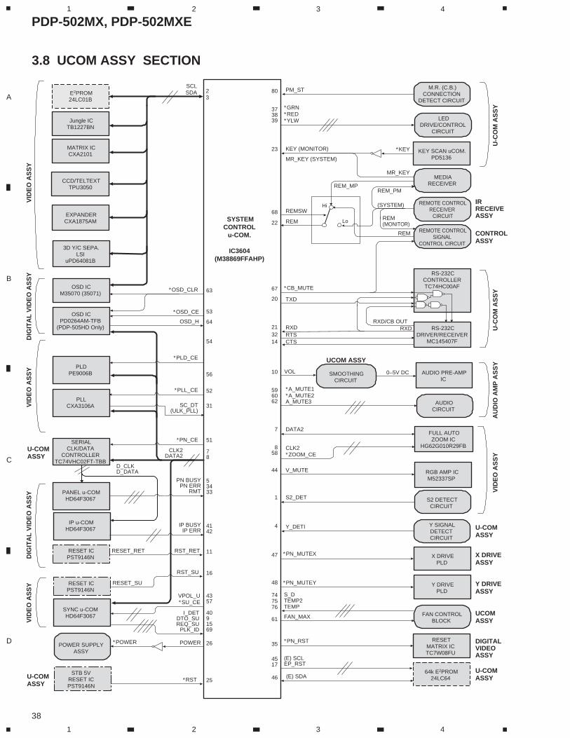
PDP-502MX, PDP-502MXE
38
A
B
C
D
1 2 3 4
1 2 3 4
3.8 UCOM ASSY SECTION
Hi
Lo
E2PROM24LC01B
64k E2PROM24LC64
RESETMATRIX ICTC7W08FU
Y SIGNALDETECTCIRCUIT
S2 DETECTCIRCUIT
RGB AMP ICM52337SP
FULL AUTOZOOM IC
HG62G010R29FB
AUDIOCIRCUIT
AUDIO PRE-AMPIC
SMOOTHINGCIRCUIT
RS-232CDRIVER/RECEIVER
MC145407F
RS-232CCONTROLLERTC74HC00AF
MEDIARECEIVER
KEY SCAN uCOM.PD5136
LEDDRIVE/CONTROL
CIRCUIT
M.R. (C.B.)CONNECTION
DETECT CIRCUIT
REMOTE CONTROLSIGNAL
CONTROL CIRCUIT
REMOTE CONTROLRECEIVER CIRCUIT
FAN CONTROLBLOCK
Y DRIVEPLD
X DRIVEPLD
23
SCLSDA
∗OSD_CLR
∗PLD_CE
∗PLL_CE
VPOL_U∗SU_CE
∗PN_CE
∗POWER
∗RST
SC_DT(ULK_PLL)
CLK2DATA2
D_CLKD_DATA
25
26
4091569
4357
16
11
4142
53433
78
51
31
52
56
54
64
53
63
80
23
68
22
67
20
213214
10
596062
7
44
1
4
47
61
35
4517
46 (E) SDA
∗PN_RST
∗PN_MUTEY
∗PN_MUTEX
FAN_MAX
(E) SCLEP_RST
S_DTEMP2TEMP
Y_DETI
S2_DET
V_MUTE
DATA2
VOL 0–5V DC
RXD RXDRXD/CB OUT
TXD
REM
REMSW
MR_KEY (SYSTEM)
REM_MPREM_PM
(SYSTEM)
REM
REM(MONITOR)
MR_KEY
PM_ST
KEY (MONITOR)
RTSCTS
CLK2∗ZOOM_CE
∗A_MUTE1∗A_MUTE2A_MUTE3
∗CB_MUTE
∗GRN∗RED∗YLW
∗KEY
48
747576
858
373839
PN BUSYPN ERR
RMT
IP BUSYIP ERR
RESET_RET RST_RET
RESET_SU
RST_SU
I_DETDTO_SUREQ_SU
PLK_ID
POWER
∗OSD_CE
OSD_H
Jungle ICTB1227BN
MATRIX ICCXA2101
VID
EO
AS
SY
VID
EO
AS
SY
AU
DIO
AM
P A
SS
YU
-CO
M A
SS
YU
-CO
M A
SS
YV
IDE
O A
SS
Y
VID
EO
AS
SY
DIG
ITA
L V
IDE
O A
SS
YD
IGIT
AL
VID
EO
AS
SY
U-COMASSY
UCOM ASSY
U-COMASSY
UCOMASSY
CONTROLASSY
IRRECEIVEASSY
U-COMASSY
Y DRIVEASSY
X DRIVEASSY
DIGITALVIDEOASSY
U-COMASSY
CCD/TELTEXTTPU3050
EXPANDERCXA1875AM
3D Y/C SEPA.LSI
uPD64081B
OSD ICM35070 (35071)
SYSTEMCONTROL
u-COM.
IC3604(M38869FFAHP)
OSD ICPD0264AM-TFB
(PDP-505HD Only)
PLDPE9006B
PLLCXA3106A
PANEL u-COMHD64F3067
IP u-COMHD64F3067
SYNC u-COMHD64F3067
POWER SUPPLYASSY
STB 5VRESET ICPST9146N
RESET ICPST9146N
RESET ICPST9146N
SERIALCLK/DATA
CONTROLLERTC74VHC02FT-TBB
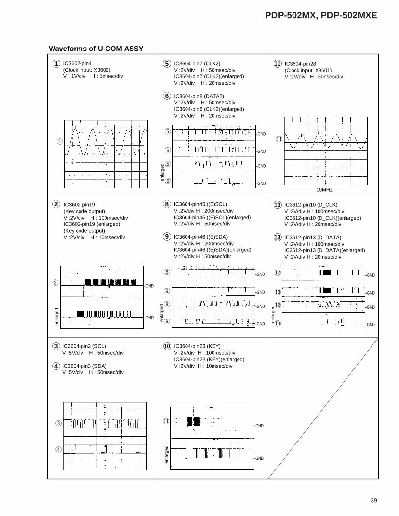
PDP-502MX, PDP-502MXE
39
Waveforms of U-COM ASSY
IC3602-pin4 (Clock input: X3602)V : 1V/div H : 1msec/div
IC3602-pin19(Key code output)V :2V/div H : 100msec/divIC3602-pin19 (enlarged)(Key code output)V :2V/div H : 10msec/div
IC3604-pin2 (SCL)V :5V/div H : 50msec/div
IC3604-pin3 (SDA)V :5V/div H : 50msec/div
IC3604-pin7 (CLK2)V :2V/div H : 50msec/divIC3604-pin7 (CLK2)(enlarged)V :2V/div H : 20msec/div
IC3604-pin8 (DATA2)V :2V/div H : 50msec/divIC3604-pin8 (CLK2)(enlarged)V :2V/div H : 20msec/div
IC3604-pin45 ((E)SCL)V :2V/div H : 200msec/divIC3604-pin45 ((E)SCL)(enlarged)V :2V/div H : 50msec/div
IC3604-pin46 ((E)SDA)V :2V/div H : 200msec/divIC3604-pin46 ((E)SDA)(enlarged)V :2V/div H : 50msec/div
IC3604-pin23 (KEY)V :2V/div H : 100msec/divIC3604-pin23 (KEY)(enlarged)V :2V/div H : 10msec/div
IC3604-pin28 (Clock input: X3601)V :2V/div H : 50nsec/div
IC3612-pin10 (D_CLK)V :2V/div H : 100msec/divIC3612-pin10 (D_CLK)(enlarged)V :2V/div H : 20msec/div
IC3612-pin13 (D_DATA)V :2V/div H : 100msec/divIC3612-pin13 (D_DATA)(enlarged)V :2V/div H : 20msec/div
13
=
-
2
-
=
–GND
–GND
–GND
10MHz
–GND
–GND
–GND
–GND
–GND
–GND
–GND
–GND
–GND
~
~
8
8
9
3
4
9
13
9
8
–GND
–GND
–GND
–GND
5
1
5
6
6
6
51
4
3
2
11
10
enla
rged
enla
rged
enla
rged
enla
rged
enla
rged
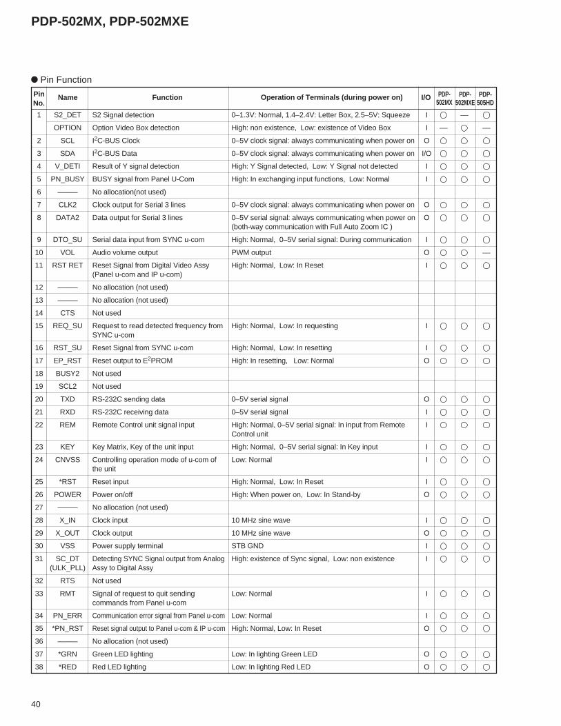
PDP-502MX, PDP-502MXE
40
1 S2_DET S2 Signal detection 0–1.3V: Normal, 1.4–2.4V: Letter Box, 2.5–5V: Squeeze I ––
OPTION Option Video Box detection High: non existence, Low: existence of Video Box I –– ––
2 SCL I2C-BUS Clock 0–5V clock signal: always communicating when power on O
3 SDA I2C-BUS Data 0–5V clock signal: always communicating when power on I/O
4 V_DETI Result of Y signal detection High: Y Signal detected, Low: Y Signal not detected I
5 PN_BUSY BUSY signal from Panel U-Com High: In exchanging input functions, Low: Normal I
6 ––––– No allocation(not used)
7 CLK2 Clock output for Serial 3 lines 0–5V clock signal: always communicating when power on O
8 DATA2 Data output for Serial 3 lines 0–5V serial signal: always communicating when power on O(both-way communication with Full Auto Zoom IC )
9 DTO_SU Serial data input from SYNC u-com High: Normal, 0–5V serial signal: During communication I
10 VOL Audio volume output PWM output O ––
11 RST RET Reset Signal from Digital Video Assy High: Normal, Low: In Reset I(Panel u-com and IP u-com)
12 ––––– No allocation (not used)
13 ––––– No allocation (not used)
14 CTS Not used
15 REQ_SU Request to read detected frequency from High: Normal, Low: In requesting ISYNC u-com
16 RST_SU Reset Signal from SYNC u-com High: Normal, Low: In resetting I
17 EP_RST Reset output to E2PROM High: In resetting, Low: Normal O
18 BUSY2 Not used
19 SCL2 Not used
20 TXD RS-232C sending data 0–5V serial signal O
21 RXD RS-232C receiving data 0–5V serial signal I
22 REM Remote Control unit signal input High: Normal, 0–5V serial signal: In input from Remote IControl unit
23 KEY Key Matrix, Key of the unit input High: Normal, 0–5V serial signal: In Key input I
24 CNVSS Controlling operation mode of u-com of Low: Normal Ithe unit
25 *RST Reset input High: Normal, Low: In Reset I
26 POWER Power on/off High: When power on, Low: In Stand-by O
27 ––––– No allocation (not used)
28 X_IN Clock input 10 MHz sine wave I
29 X_OUT Clock output 10 MHz sine wave O
30 VSS Power supply terminal STB GND I
31 SC_DT Detecting SYNC Signal output from Analog High: existence of Sync signal, Low: non existence I(ULK_PLL) Assy to Digital Assy
32 RTS Not used
33 RMT Signal of request to quit sending Low: Normal Icommands from Panel u-com
34 PN_ERR Communication error signal from Panel u-com Low: Normal I
35 *PN_RST Reset signal output to Panel u-com & IP u-com High: Normal, Low: In Reset O
36 ––––– No allocation (not used)
37 *GRN Green LED lighting Low: In lighting Green LED O
38 *RED Red LED lighting Low: In lighting Red LED O
Pin Function
PinNo.
Name Function Operation of Terminals (during power on) I/O PDP-502MXE
PDP-505HD
PDP-502MX
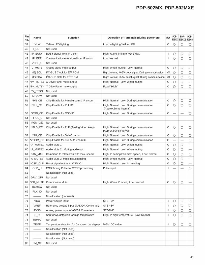
PDP-502MX, PDP-502MXE
41
39 *YLW Yellow LED lighting Low: In lighting Yellow LED O
40 I_DET Not used
41 IP_BUSY BUSY signal from IP u-com High: At the timing of VD SYNC I
42 IP_ERR Communication error signal from IP u-com Low: Normal I
43 VPOL_U Not used
44 V_MUTE Analog video mute output High: When muting, Low: Normal O
45 (E) SCL I2C-BUS Clock for E2PROM High: Normal, 0–5V clock signal: During communication I/O
46 (E) SDA I2C-BUS Data for E2PROM High: Normal, 0–5V serial signal: During communication I/O
47 *PN_MUTEX X Drive Panel mute output High: Normal, Low: When muting O
48 *PN_MUTEY Y Drive Panel mute output Fixed "High" O
49 *V_STDO Not used
50 STDSW Not used
51 *PN_CE Chip Enable for Panel u-com & IP u-com High: Normal, Low: During communication O
52 *PLL_CE Chip Enable for PLL IC High: Normal, Low: During communication O (Approx.80ms interval)
53 *OSD_CE Chip Enable for OSD IC High: Normal, Low: During communication O –– ––
54 HPOL_U Not used
55 PGM_OE Not used
56 *PLD_CE Chip Enable for PLD (Analog Video Assy) High: Normal, Low: During communication O(Approx.80ms interval)
57 *SU_CE Chip Enable for SYNC u-com High: Normal, Low: During communication O
58 *ZOOM_CE Chip Enable for Full Auto Zoom IC High: Normal, Low: During communication O –– ––
59 *A_MUTE1 Audio Mute 1 High: Normal, Low: When muting O ––
60 *A_MUTE2 Audio Mute 2 Muting audio out High: Normal, Low: When muting O ––
61 FAN_MAX Command to rotate Fan with max. speed High: In setting Fan max. speed, Low: Normal O
62 A_MUTE3 Audio Mute 3 Mute in suspending High: When muting, Low: Normal O ––
63 *OSD_CLR Reset signal output to OSD IC High: Normal, Low: In resetting O ––
64 OSD_H OSD Timing Pulse for SYNC processing Pulse input I –– ––
65 ––––– No allocation (Not used)
66 DRV_OFF Not used
67 *CB_MUTE Combination Mute High: When ID is set, Low: Normal O ––
68 REMSW Not used
69 PLK_ID Not used
70 ––––– No allocation (not used)
71 VCC Power source input STB +5V I
72 VREF Reference voltage input of AD/DA Converters STB +5V I
73 AVSS Analog power input of AD/DA Converters STBGND I
74 S_D Shut down detection for high temperature High: In high temperature, Low: Normal I
75 TEMP2 Not used
76 TEMP Temperature detection for On screen bar display 0–5V DC value I
77 ––––– No allocation (Not used)
78 ––––– No allocation (Not used)
79 ––––– No allocation (Not used)
80 PM_ST Not used
PinNo.
Name Function Operation of Terminals (during power on) I/O PDP-502MXE
PDP-505HD
PDP-502MX
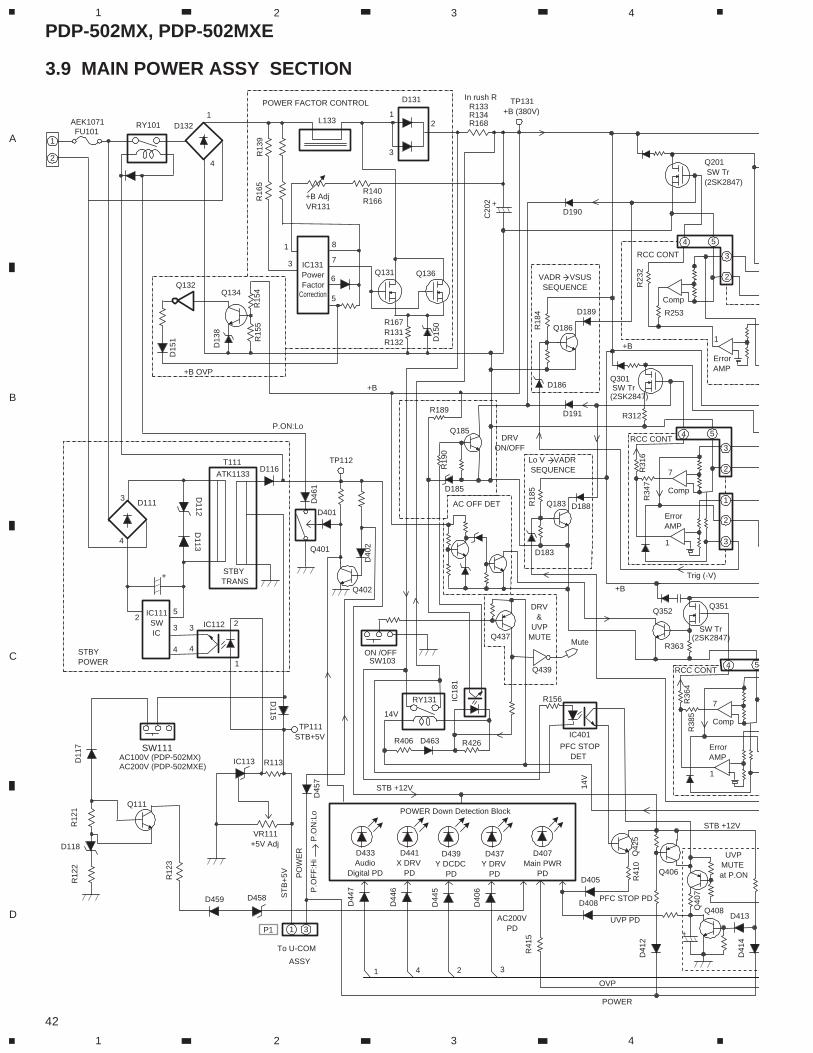
PDP-502MX, PDP-502MXE
42
A
B
C
D
1 2 3 4
1 2 3 4
FU1011
2
D113
+
D112
D115
R12
1D
117
R12
2
D116
R167R131R132
R133R134R168
Q132
D15
1
D132RY101 L133
D131
1
4
1
3
2
In rush R
Q136Q131
D15
0
+B AdjVR131
R140R166
IC131PowerFactor
Correction
1
3
8
6
7
5Q134
R15
4R
155
D13
8
4
D111
ATK1133
T111
STBY TRANS
IC1123
4
1
2
IC113 R113
VR111+5V Adj
SW111AC100V (PDP-502MX)AC200V (PDP-502MXE)
D118
Q111
4
3
52
IC111SWIC
3
R12
3
TP112
Q401
D401
Q402
D40
2
TP111STB+5V
STB +12V
D458D459
AC200VPD
D45
7
OVP
P.ON:Lo
RY131
POWER Down Detection Block
D433Audio
Digital PD
D441X DRV
PD
D439Y DCDC
PD
D437Y DRV
PD
D407Main PWR
PD
+B OVP
1 3
ST
B+
5V PO
WE
R
To U-COM
ASSY
P1
1 2 34
D408
+
UVP PD
R41
5
D44
7
D44
6
D44
5
D40
6
POWER
D413
D41
4
Q408Q40
7
D41
2
Q406
STB +12V
UVPMUTEat P.ON
D405
PFC STOP PD
IC401
Q42
5R
410
P.O
FF
:Hi
P.O
N:L
o
AEK1071
14V
14V
D463R406
SW103ON /OFF
Q437
Q439
DRV&
UVP MUTE
R426 PFC STOPDET
R156
ErrorAMP
Comp
R36
4R
385
54RCC CONT
1
7
1
2ErrorAMP
Comp
R31
6R
347
2
3
54
3
RCC CONT
1
7
Trig (-V)
+
ErrorAMP
Comp
2
54
1
3
R23
2
R253
D188Q183
D183
D189
Q186
D186
D191
D190
Q185
D185
R19
0
R189
C20
2
R18
5R
184
DRVON/OFF
VADR VSUSSEQUENCE
Lo V VADRSEQUENCE
Q201 SW Tr(2SK2847)
Q301 SW Tr(2SK2847)
SW Tr(2SK2847)
RCC CONT
POWER FACTOR CONTROL
D46
1
STBYPOWER
IC18
1
R16
5R
139
R312
R363
Q351Q352
Mute
AC OFF DET
TP131+B (380V)
+B
+B
+B
3.9 MAIN POWER ASSY SECTION
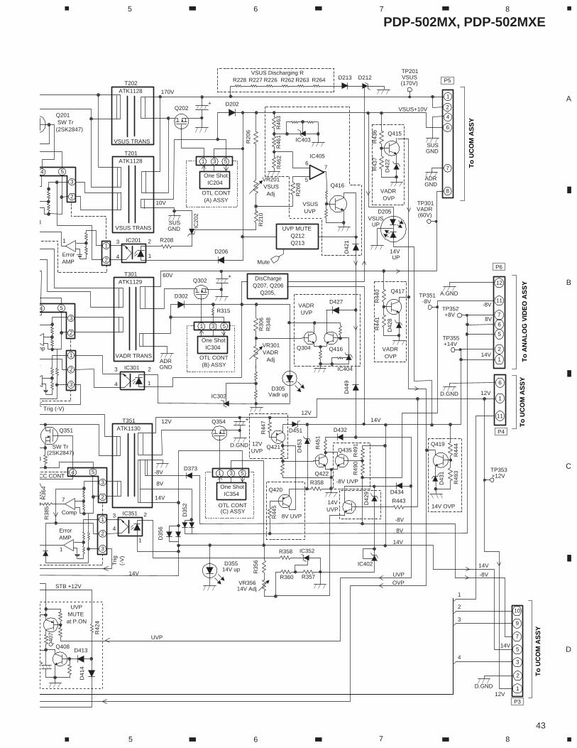
PDP-502MX, PDP-502MXE
43
A
B
C
D
5 6 7 8
5 6 7 8
VADROVP
VADROVP
T202ATK1128
IC2013
4
2
1
+
One ShotIC204
SUSGND IC
202
R208
D202
D206R
206
VR201VSUS
AdjOTL CONT(A) ASSY
R21
0
Q202
T301ATK1129
+
One ShotIC304
ADRGND
IC302
D302
R30
6R
348
VR301VADR
AdjOTL CONT(B) ASSY
Q302
R315
D305Vadr up
R46
3
6
5
7
IC405
R46
2R
461
IC403
Q416
Q304 Q416
D427VADRUVP
VSUSUVP
D42
1
R26
8
T351ATK1130
IC3513
4
2
1
+
One ShotIC354
R35
6
OTL CONT(C) ASSY
Q354
IC352
Q422
Q435
D35
6
14V
8V
-8V
12V
60V
170V
D35
2
D373
R358
R360 R357VR356
14V Adj
Q421
Q420
R44
5
R358
8V UVP
D44
9
D451
D45
3
D432
R49
1R
490
R44
7
R45
1
R443
D434
D42
9
IC402
14V
D35514V up
12V
-8V UVP
14VUVP 14V OVP
Q415
R43
6R
437
D42
2
Q417
R44
0R
441
D42
8
IC404
12VUVP
Q419
R44
4R
493
D43
1
10V
1 3 5
1 3 5
1 3 5
D205VSUS
UP
1
SUSGND
ADRGND
P5
T201ATK1128
14V UP
R228 R227 R226 R262 R263 R264 D213 D212
VSUS+10V
DisChargeQ207, Q206
Q205,
VSUS Discharging R
P6
2
4
6
7
8
D.GND
-8V
8V
14V
11
7
6
5
2
1
1
6
11
D.GND
12V
P4
A.GND
12
7
5
3
2
1
9
10
P312V
D.GND
-8V
14V
8V
UVPOVP
14V
-8V
1
2
3
4
14V
+
D413
D41
4
Q408Q40
7
STB +12V
UVPMUTEat P.ON
R42
4
1
2
1
2
ErrorAMP
Comp
R36
4R
385
2
3
54
3
CC CONT
1
7
Trig
(-V
)
1
2r
mp
2
3
54
3
Trig (-V)
IC3013
4
2
1
ErrorAMP
2
54
1
3
3
VADR TRANS
VSUS TRANS
VSUS TRANS
Q201 SW Tr(2SK2847)
SW Tr(2SK2847)
3
Q351
UVP MUTEQ212Q213
Mute
UVP
TP201VSUS(170V)
TP301VADR(60V)
TP351-8V
TP352+8V
TP355+14V
TP353+12V
14V
To
UC
OM
AS
SY
To
UC
OM
AS
SY
To
UC
OM
AS
SY
To
AN
AL
OG
VID
EO
AS
SY
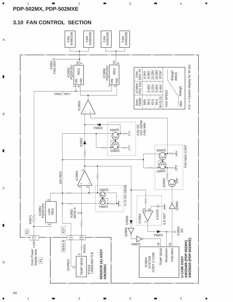
PDP-502MX, PDP-502MXE
44
A
B
C
D
1 2 3 4
1 2 3 4
TE
MP
SE
NS
IC41
01
R
EG
VIN
Vo
Vad
IC39
52P
Q20
VZ
IUF
AN
AX
M10
36
+ –
IC39
54
SE
NS
A
3
10V
RE
G1
1
E27
LM50
CIM
3-T
LB
SE
NS
OR
(A
) A
SS
YA
WZ
6501
K39
52S
EN
S A
21
23
R41
51D
3952
IC39
53
Fro
m P
ower
Sup
ply
assy
0.7V
DC
GE
NE
FA
N M
AX
CO
NT
Q39
59
Q39
60
R
EG
VIN
Vo
Vad
IC39
56P
Q20
VZ
IU
+–
+ –
1 1 44
33
7+
14V
P1
E2
R39
71
+10
VR
EG
IC39
51P
Q20
VZ
IU
13
4.5V
DC
FA
N M
INV
OL
GE
NE
10V
RE
G
61
Q39
66
IC36
04S
YS
TE
MC
ON
T U
-CO
M
Q3962
D3953
Q3957
Q3951
Q3952
Q3953
Q3954D3951
+14V_FAN1
Q3958
FA
N M
AX
Shu
tDow
n
TE
MP
SE
NS
76
D39
59
57
6
IC39
54
K39
54S
DU
-CO
M A
SS
YA
WZ
6499
(P
DP
-502
MX
)A
WZ
6520
(P
DP
-502
MX
E)
EN
V.
TE
MP
MIN
30.0
43.0
45.0
50 (
S.D
)
IC39
54P
in1
Out
4.45
V5.
22V
5.55
V6.
46V
FA
ND
RV
TP
6.04
V6.
08V
13.2
8V16
.58V
ST
OP
MIN
30de
gC
45de
gC(M
AX
)
FA
N S
PE
ED
S.D
= C
autio
n di
spla
y fo
r 30
sec
.
6.5V
DC
S.D
DE
T
K39
51F
AN
DR
V
FA
NA
XM
1036
FA
NA
XM
1036
FA
NA
XM
1036
3.10 FAN CONTROL SECTION

PDP-502MX, PDP-502MXE
45
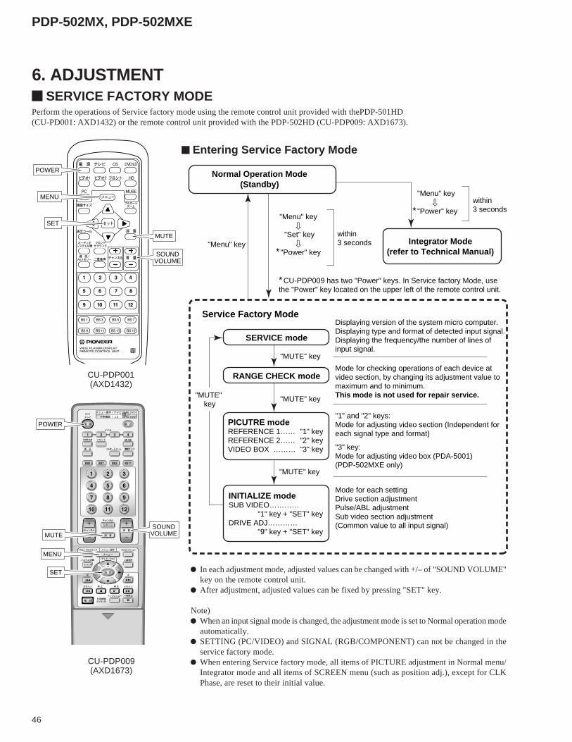
PDP-502MX, PDP-502MXE
46
SERVICE FACTORY MODEPerform the operations of Service factory mode using the remote control unit provided with thePDP-501HD(CU-PD001: AXD1432) or the remote control unit provided with the PDP-502HD (CU-PDP009: AXD1673).
POWER
MENU
SET
MUTE
SOUNDVOLUME
POWER
MENU
SET
MUTESOUND
VOLUME
Normal Operation Mode(Standby)
Service Factory Mode
SERVICE mode
RANGE CHECK mode
Integrator Mode (refer to Technical Manual)
PICUTRE modeREFERENCE 1…… "1" keyREFERENCE 2…… "2" keyVIDEO BOX ……… "3" key
INITIALIZE modeSUB VIDEO………… "1" key + "SET" keyDRIVE ADJ………… "9" key + "SET" key
"Menu" key‘
"Set" key‘
∗"Power" key
"Menu" key‘
∗"Power" key
"Menu" key
"MUTE" key
"MUTE" key"MUTE" key
"MUTE" key
within3 seconds
within3 seconds
∗CU-PDP009 has two "Power" keys. In Service factory Mode, use the "Power" key located on the upper left of the remote control unit.
Mode for checking operations of each device at video section, by changing its adjustment value to maximum and to minimum.This mode is not used for repair service.
Displaying version of the system micro computer.Displaying type and format of detected input signal.Displaying the frequency/the number of lines of input signal.
"1" and "2" keys:Mode for adjusting video section (Independent for each signal type and format)
"3" key:Mode for adjusting video box (PDA-5001)(PDP-502MXE only)
Mode for each setting Drive section adjustment Pulse/ABL adjustmentSub video section adjustment (Common value to all input signal)
CU-PDP001(AXD1432)
CU-PDP009(AXD1673)
Entering Service Factory Mode
In each adjustment mode, adjusted values can be changed with +/– of "SOUND VOLUME"key on the remote control unit.After adjustment, adjusted values can be fixed by pressing "SET" key.
Note)When an input signal mode is changed, the adjustment mode is set to Normal operation modeautomatically.SETTING (PC/VIDEO) and SIGNAL (RGB/COMPONENT) can not be changed in theservice factory mode.When entering Service factory mode, all items of PICTURE adjustment in Normal menu/Integrator mode and all items of SCREEN menu (such as position adj.), except for CLKPhase, are reset to their initial value.
6. ADJUSTMENT
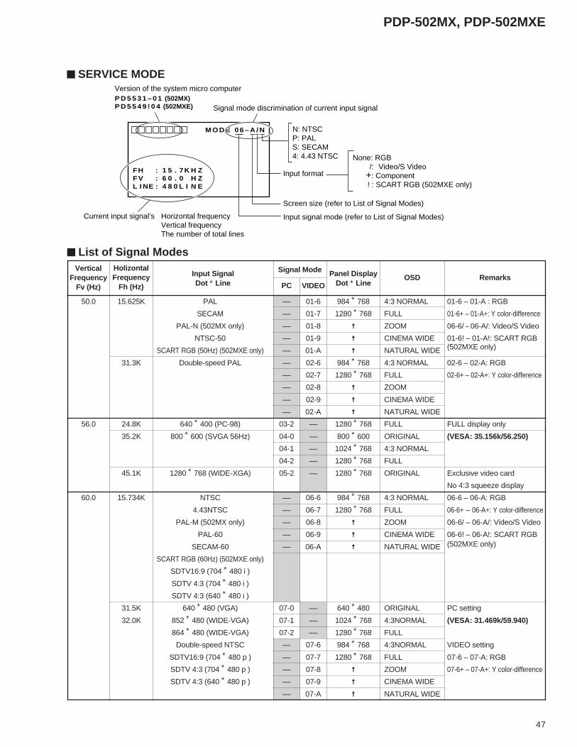
PDP-502MX, PDP-502MXE
47
SERVICE MODE
P D 5 5 3 1 – 0 1 M O D E 0 6 – A / N
P D 5 5 3 1 – 0 1 (502MX)P D 5 5 4 9 ! 0 4 (502MXE)
FH : 1 5 . 7 K H ZF V : 6 0 . 0 H ZL I NE : 4 8 0 L I N E
Version of the system micro computer
Signal mode discrimination of current input signal
Input format
Screen size (refer to List of Signal Modes)
Input signal mode (refer to List of Signal Modes)
N: NTSCP: PALS: SECAM4: 4.43 NTSC None: RGB
/: Video/S Video +: Component ! : SCART RGB (502MXE only)
Current input signal’s Horizontal frequencyVertical frequencyThe number of total lines
List of Signal ModesVertical
FrequencyFv (Hz)
HolizontalFrequency
Fh (Hz)Remarks
Signal Mode
PC VIDEO
Input SignalDot ∗ Line
Panel DisplayDot ∗ Line
OSD
50.0 15.625K PAL –– 01-6 984 ∗ 768 4:3 NORMAL 01-6 – 01-A : RGB
SECAM –– 01-7 1280 ∗ 768 FULL 01-6+ – 01-A+: Y color-difference
PAL-N (502MX only) –– 01-8 ± ZOOM 06-6/ – 06-A/: Video/S Video
NTSC-50 –– 01-9 ± CINEMA WIDE 01-6! – 01-A!: SCART RGB
SCART RGB (50Hz) (502MXE only) –– 01-A ± NATURAL WIDE (502MXE only)
31.3K Double-speed PAL –– 02-6 984 ∗ 768 4:3 NORMAL 02-6 – 02-A: RGB
–– 02-7 1280 ∗ 768 FULL 02-6+ – 02-A+: Y color-difference
–– 02-8 ± ZOOM
–– 02-9 ± CINEMA WIDE
–– 02-A ± NATURAL WIDE
56.0 24.8K 640 ∗ 400 (PC-98) 03-2 –– 1280 ∗ 768 FULL FULL display only
35.2K 800 ∗ 600 (SVGA 56Hz) 04-0 –– 800 ∗ 600 ORIGINAL (VESA: 35.156k/56.250)
04-1 –– 1024 ∗ 768 4:3 NORMAL
04-2 –– 1280 ∗ 768 FULL
45.1K 1280 ∗ 768 (WIDE-XGA) 05-2 –– 1280 ∗ 768 ORIGINAL Exclusive video card
No 4:3 squeeze display
60.0 15.734K NTSC –– 06-6 984 ∗ 768 4:3 NORMAL 06-6 – 06-A: RGB
4.43NTSC –– 06-7 1280 ∗ 768 FULL 06-6+ – 06-A+: Y color-difference
PAL-M (502MX only) –– 06-8 ± ZOOM 06-6/ – 06-A/: Video/S Video
PAL-60 –– 06-9 ± CINEMA WIDE 06-6! – 06-A!: SCART RGB
SECAM-60 –– 06-A ± NATURAL WIDE (502MXE only)
SCART RGB (60Hz) (502MXE only)
SDTV16:9 (704 ∗ 480 i )
SDTV 4:3 (704 ∗ 480 i )
SDTV 4:3 (640 ∗ 480 i )
31.5K 640 ∗ 480 (VGA) 07-0 –– 640 ∗ 480 ORIGINAL PC setting
32.0K 852 ∗ 480 (WIDE-VGA) 07-1 –– 1024 ∗ 768 4:3NORMAL (VESA: 31.469k/59.940)
864 ∗ 480 (WIDE-VGA) 07-2 –– 1280 ∗ 768 FULL
Double-speed NTSC –– 07-6 984 ∗ 768 4:3NORMAL VIDEO setting
SDTV16:9 (704 ∗ 480 p ) –– 07-7 1280 ∗ 768 FULL 07-6 – 07-A: RGB
SDTV 4:3 (704 ∗ 480 p ) –– 07-8 ± ZOOM 07-6+ – 07-A+: Y color-difference
SDTV 4:3 (640 ∗ 480 p ) –– 07-9 ± CINEMA WIDE
–– 07-A ± NATURAL WIDE
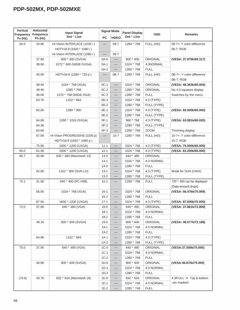
PDP-502MX, PDP-502MXE
48
VerticalFrequency
Fv (Hz)
HolizontalFrequency
Fh (Hz)Remarks
Signal Mode
PC VIDEO
Input SignalDot ∗ Line
Panel DisplayDot ∗ Line
OSD
60.0 33.8K Hi-Vision INTERLACE (1035 i ) –– 08-7 1280 ∗ 768 FULL (HD) 08-7+: Y color-difference
HDTV16:9 (1920 ∗ 1080 i ) 08-7: RGB
Hi-Vision INTERLACE (1080 i ) –– 09-7
37.9K 800 ∗ 600 (SVGA) 0A-0 –– 800 ∗ 600 ORIGINAL (VESA: 37.879k/60.317)
38.0K 1072 ∗ 600 (WIDE-SVGA) 0A-1 –– 1024 ∗ 768 4:3NORMAL
0A-2 –– 1280 ∗ 768 FULL
45.0K HDTV16:9 (1280 ∗ 720 p ) –– 0B-7 1280 ∗ 768 FULL (HD) 0B-7+: Y color-difference
0B-7: RGB
48.4K 1024 ∗ 768 (XGA) 0C-1 –– 1024 ∗ 768 ORIGINAL (VESA: 48.363k/60.004)
48.4K 1280 ∗ 768 0C-2 –– 1280 ∗ 768 ORIGINAL No 4:3 squeeze display
48.0K 1376 ∗ 768 (WIDE-XGA) 0C-2 –– 1280 ∗ 768 FULL Switches by the menu
53.7K 1152 ∗ 864 0D-1 –– 1024 ∗ 768 4:3 (TYPE)
0D-2 –– 1280 ∗ 768 FULL (TYPE)
60.0K 1280 ∗ 960 0E-1 –– 1024 ∗ 768 4:3 (TYPE) (VESA: 60.000k/60.000)
0E-2 –– 1280 ∗ 768 FULL (TYPE)
64.0K 1280 ∗ 1024 (SXGA) 0F-1 –– 960 ∗ 768 4:3 (TYPE) (VESA: 63.981k/60.020)
64.3K 0F-2 –– 1280 ∗ 768 FULL (TYPE)
64.6K 0F-3 –– 1280 ∗ 768 ZOOM Trimming display
67.5K Hi-Vision PROGRESSIVE (1035 p) –– 10-7 1280 ∗ 768 FULL (HD) 10-7+: Y color-difference
HDTV16:9 (1920 ∗ 1080 p ) 10-7: RGB
75.0K 1600 ∗ 1200 (UXGA) 11-1 –– 1024 ∗ 768 4:3 (TYPE) (VESA: 75.000k/60.000)
65.0 81.3K 1600 ∗ 1200 (UXGA) 12-1 –– 1024 ∗ 768 4:3 (TYPE) (VESA: 81.250k/65.000)
66.7 35.0K 640 ∗ 480 (Macintosh 13) 14-0 –– 640 ∗ 480 ORIGINAL
14-1 –– 1024 ∗ 768 4:3 NORMAL
14-2 –– 1280 ∗ 768 FULL
62.0K 1152 ∗ 900 (SUN LO) 13-1 –– 1024 ∗ 768 4:3 (TYPE) Mode for SUN (UNIX)
13-2 –– 1280 ∗ 768 FULL (TYPE)
70.1 31.5K 640 ∗ 400 (PC-H98) 15-2 –– 1280 ∗ 768 FULL 720 ∗ 400 can be displayed
(Data amount drops)
56.5K 1024 ∗ 768 (XGA) 16-1 –– 1024 ∗ 768 ORIGINAL (VESA: 56.476k/70.069)
16-2 –– 1280 ∗ 768 FULL
87.5K 1600 ∗ 1200 (UXGA) 17-1 –– 1024 ∗ 768 4:3 (TYPE) (VESA: 87.500k/70.000)
72.0 37.9K 640 ∗ 480 (VGA) 18-0 –– 640 ∗ 480 ORIGINAL (VESA: 37.861k/72.809)
18-1 –– 1024 ∗ 768 4:3 NORMAL
18-2 –– 1280 ∗ 768 FULL
48.1K 800 ∗ 600 (SVGA) 19-0 –– 800 ∗ 600 ORIGINAL (VESA: 48.077k/72.188)
19-1 –– 1024 ∗ 768 4:3 NORMAL
19-2 –– 1280 ∗ 768 FULL
64.9K 1152 ∗ 864 1A-1 –– 1024 ∗ 768 4:3 (TYPE)
1A-2 –– 1280 ∗ 768 FULL (TYPE)
75.0 37.5K 640 ∗ 480 (VGA) 1C-0 –– 640 ∗ 480 ORIGINAL (VESA:37.500k/75.000)
1C-1 –– 1024 ∗ 768 4:3 NORMAL
1C-2 –– 1280 ∗ 768 FULL
46.9K 800 ∗ 600 (SVGA) 1D-0 –– 800 ∗ 600 ORIGINAL (VESA:46.875k/75.000)
1D-1 –– 1024 ∗ 768 4:3 NORMAL
1D-2 –– 1280 ∗ 768 FULL
(74.6) 49.7K 832 ∗ 624 (Macintosh 16) 1E-0 –– 832 ∗ 624 ORIGINAL 4:3/FULL = Top & bottom
1E-1 –– 1024 ∗ 748 4:3 NORMAL are masked
1E-2 –– 1280 ∗ 748 FULL
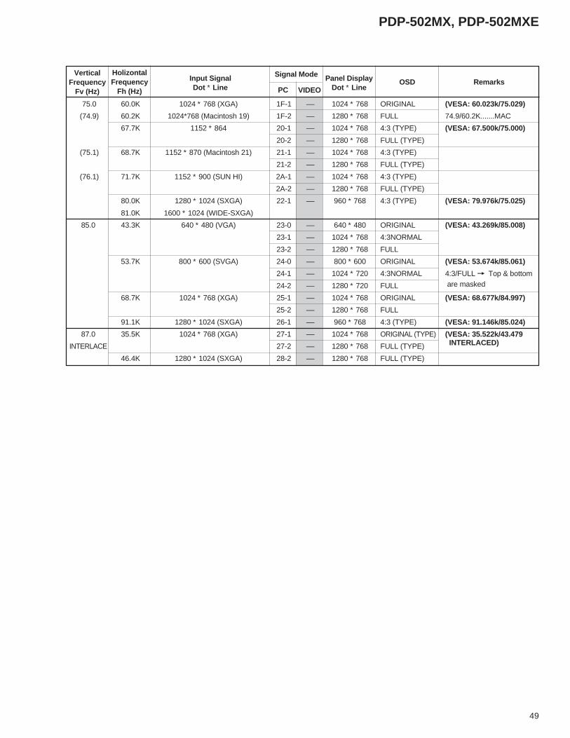
PDP-502MX, PDP-502MXE
49
VerticalFrequency
Fv (Hz)
HolizontalFrequency
Fh (Hz)Remarks
Signal Mode
PC VIDEO
Input SignalDot ∗ Line
Panel DisplayDot ∗ Line
OSD
75.0 60.0K 1024 ∗ 768 (XGA) 1F-1 –– 1024 ∗ 768 ORIGINAL (VESA: 60.023k/75.029)
(74.9) 60.2K 1024*768 (Macintosh 19) 1F-2 –– 1280 ∗ 768 FULL 74.9/60.2K.......MAC
67.7K 1152 ∗ 864 20-1 –– 1024 ∗ 768 4:3 (TYPE) (VESA: 67.500k/75.000)
20-2 –– 1280 ∗ 768 FULL (TYPE)
(75.1) 68.7K 1152 ∗ 870 (Macintosh 21) 21-1 –– 1024 ∗ 768 4:3 (TYPE)
21-2 –– 1280 ∗ 768 FULL (TYPE)
(76.1) 71.7K 1152 ∗ 900 (SUN HI) 2A-1 –– 1024 ∗ 768 4:3 (TYPE)
2A-2 –– 1280 ∗ 768 FULL (TYPE)
80.0K 1280 ∗ 1024 (SXGA) 22-1 –– 960 ∗ 768 4:3 (TYPE) (VESA: 79.976k/75.025)
81.0K 1600 ∗ 1024 (WIDE-SXGA)
85.0 43.3K 640 ∗ 480 (VGA) 23-0 –– 640 ∗ 480 ORIGINAL (VESA: 43.269k/85.008)
23-1 –– 1024 ∗ 768 4:3NORMAL
23-2 –– 1280 ∗ 768 FULL
53.7K 800 ∗ 600 (SVGA) 24-0 –– 800 ∗ 600 ORIGINAL (VESA: 53.674k/85.061)
24-1 –– 1024 ∗ 720 4:3NORMAL 4:3/FULL = Top & bottom
24-2 –– 1280 ∗ 720 FULL are masked
68.7K 1024 ∗ 768 (XGA) 25-1 –– 1024 ∗ 768 ORIGINAL (VESA: 68.677k/84.997)
25-2 –– 1280 ∗ 768 FULL
91.1K 1280 ∗ 1024 (SXGA) 26-1 –– 960 ∗ 768 4:3 (TYPE) (VESA: 91.146k/85.024)
87.0 35.5K 1024 ∗ 768 (XGA) 27-1 –– 1024 ∗ 768 ORIGINAL (TYPE) (VESA: 35.522k/43.479
INTERLACE 27-2 –– 1280 ∗ 768 FULL (TYPE) INTERLACED)
46.4K 1280 ∗ 1024 (SXGA) 28-2 –– 1280 ∗ 768 FULL (TYPE)
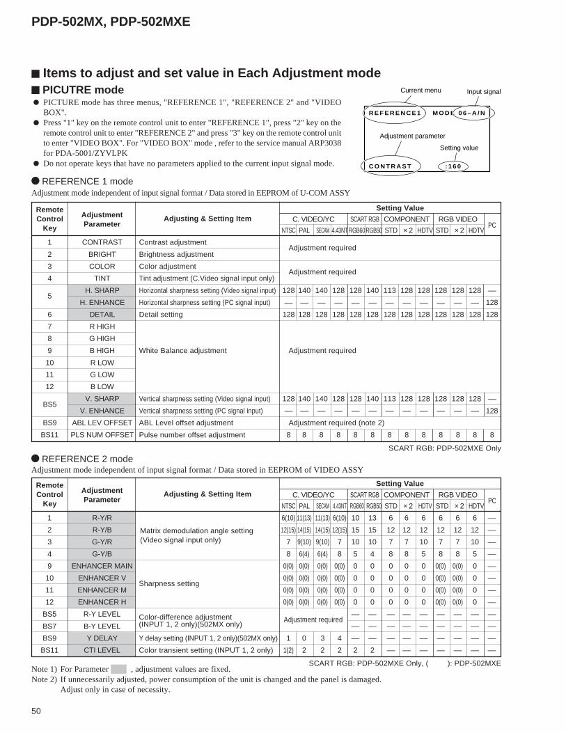
PDP-502MX, PDP-502MXE
50
C. VIDEO/YC SCART RGB COMPONENT RGB VIDEO
NTSC PAL SECAM 4.43NT RGB60RGB50 STD × 2 HDTV STD × 2 HDTVPC
RemoteControl
Key
AdjustmentParameter
Adjusting & Setting ItemSetting Value
REFERENCE 1 mode
C O N T R A S T : 1 6 0
R E F E R E N C E 1 M O D E 0 6 – A / N
Adjustment parameter
Current menu Input signal
Setting value
Items to adjust and set value in Each Adjustment mode PICUTRE mode
Adjustment mode independent of input signal format / Data stored in EEPROM of U-COM ASSY
C. VIDEO/YC SCART RGB COMPONENT RGB VIDEO
NTSC PAL SECAM 4.43NT RGB60 RGB50 STD × 2 HDTV STD × 2 HDTVPC
RemoteControl
Key
AdjustmentParameter
Adjusting & Setting ItemSetting Value
REFERENCE 2 modeAdjustment mode independent of input signal format / Data stored in EEPROM of VIDEO ASSY
Note 1) For Parameter , adjustment values are fixed.Note 2) If unnecessarily adjusted, power consumption of the unit is changed and the panel is damaged.
Adjust only in case of necessity.
PICTURE mode has three menus, "REFERENCE 1", "REFERENCE 2" and "VIDEOBOX".
Press "1" key on the remote control unit to enter "REFERENCE 1", press "2" key on theremote control unit to enter "REFERENCE 2" and press "3" key on the remote control unitto enter "VIDEO BOX". For "VIDEO BOX" mode , refer to the service manual ARP3038for PDA-5001/ZYVLPK
Do not operate keys that have no parameters applied to the current input signal mode.
Matrix demodulation angle setting(Video signal input only)
1 R-Y/R 6(10) 11(13) 11(13) 6(10) 10 13 6 6 6 6 6 6 ––
2 R-Y/B 12(15) 14(15) 14(15) 12(15) 15 15 12 12 12 12 12 12 ––
3 G-Y/R 7 9(10) 9(10) 7 10 10 7 7 10 7 7 10 ––
4 G-Y/B 8 6(4) 6(4) 8 5 4 8 8 5 8 8 5 ––
9 ENHANCER MAIN 0(0) 0(0) 0(0) 0(0) 0 0 0 0 0 0(0) 0(0) 0 ––
10 ENHANCER V 0(0) 0(0) 0(0) 0(0) 0 0 0 0 0 0(0) 0(0) 0 ––Sharpness setting
11 ENHANCER M 0(0) 0(0) 0(0) 0(0) 0 0 0 0 0 0(0) 0(0) 0 ––
12 ENHANCER H 0(0) 0(0) 0(0) 0(0) 0 0 0 0 0 0(0) 0(0) 0 ––
BS5 R-Y LEVEL –– –– –– –– –– –– –– –– ––Color-difference adjustment Adjustment requiredBS7 B-Y LEVEL (INPUT 1, 2 only)(502MX only) –– –– –– –– –– –– –– –– ––
BS9 Y DELAY Y delay setting (INPUT 1, 2 only)(502MX only) 1 0 3 4 –– –– –– –– –– –– –– –– ––
BS11 CTI LEVEL Color transient setting (INPUT 1, 2 only) 1(2) 2 2 2 2 2 –– –– –– –– –– –– ––
1 CONTRAST Contrast adjustmentAdjustment required
2 BRIGHT Brightness adjustment
3 COLOR Color adjustmentAdjustment required
4 TINT Tint adjustment (C.Video signal input only)
H. SHARP Horizontal sharpness setting (Video signal input) 128 140 140 128 128 140 113 128 128 128 128 128 ––5
H. ENHANCE Horizontal sharpness setting (PC signal input) –– –– –– –– –– –– –– –– –– –– –– –– 128
6 DETAIL Detail setting 128 128 128 128 128 128 128 128 128 128 128 128 128
7 R HIGH
8 G HIGH
9 B HIGH White Balance adjustment Adjustment required
10 R LOW
11 G LOW
12 B LOW
V. SHARP Vertical sharpness setting (Video signal input) 128 140 140 128 128 140 113 128 128 128 128 128 ––BS5
V. ENHANCE Vertical sharpness setting (PC signal input) –– –– –– –– –– –– –– –– –– –– –– –– 128
BS9 ABL LEV OFFSET ABL Level offset adjustment Adjustment required (note 2)
BS11 PLS NUM OFFSET Pulse number offset adjustment 8 8 8 8 8 8 8 8 8 8 8 8 8
SCART RGB: PDP-502MXE Only, ( ): PDP-502MXE
SCART RGB: PDP-502MXE Only
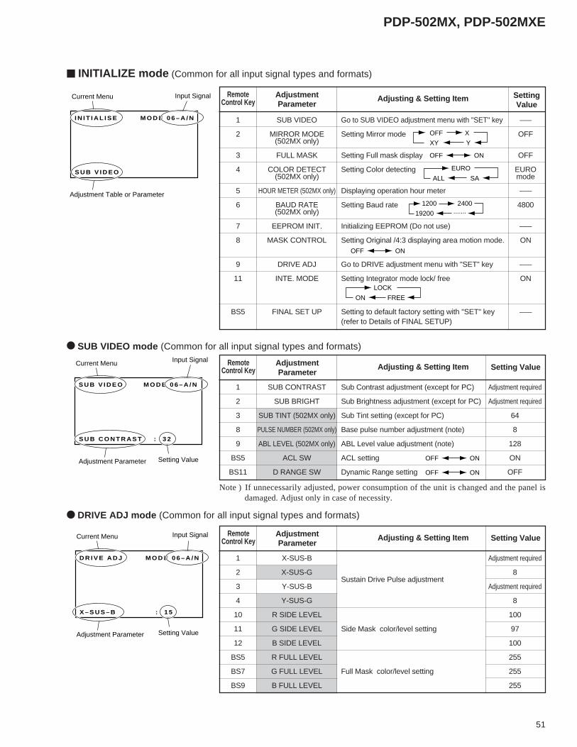
PDP-502MX, PDP-502MXE
51
1 SUB CONTRAST Sub Contrast adjustment (except for PC) Adjustment required
2 SUB BRIGHT Sub Brightness adjustment (except for PC) Adjustment required
3 SUB TINT (502MX only) Sub Tint setting (except for PC) 64
8 PULSE NUMBER (502MX only) Base pulse number adjustment (note) 8
9 ABL LEVEL (502MX only) ABL Level value adjustment (note) 128
BS5 ACL SW ACL setting ON
BS11 D RANGE SW Dynamic Range setting OFF
INITIALIZE mode (Common for all input signal types and formats)
S U B V I D E O
Adjustment Table or Parameter
Current Menu Input Signal
I N I T I A L I S E M O D E 0 6 – A / N 1 SUB VIDEO Go to SUB VIDEO adjustment menu with "SET" key –––
2 MIRROR MODE Setting Mirror mode OFF(502MX only)
3 FULL MASK Setting Full mask display OFF
4 COLOR DETECT Setting Color detecting EURO(502MX only) mode
5 HOUR METER (502MX only) Displaying operation hour meter –––
6 BAUD RATE Setting Baud rate 4800(502MX only)
7 EEPROM INIT. Initializing EEPROM (Do not use) –––
8 MASK CONTROL Setting Original /4:3 displaying area motion mode. ON
9 DRIVE ADJ Go to DRIVE adjustment menu with "SET" key –––
11 INTE. MODE Setting Integrator mode lock/ free ON
BS5 FINAL SET UP Setting to default factory setting with "SET" key –––(refer to Details of FINAL SETUP)
OFF X
XY Y
OFF ON
EURO
ALL SA
1200 2400
19200 .......
OFF ON
LOCK
ON FREE
SUB VIDEO mode (Common for all input signal types and formats)
S U B C O N T R A S T : 3 2
Adjustment Parameter Setting Value
Current Menu Input Signal
S U B V I D E O M O D E 0 6 – A / N
OFF ON
OFF ON
DRIVE ADJ mode (Common for all input signal types and formats)
X – S U S – B : 1 5
Adjustment Parameter Setting Value
Current Menu Input Signal
D R I V E A D J M O D E 0 6 – A / N
Note ) If unnecessarily adjusted, power consumption of the unit is changed and the panel isdamaged. Adjust only in case of necessity.
RemoteControl Key
AdjustmentParameter
Adjusting & Setting Item SettingValue
RemoteControl Key
AdjustmentParameter
Adjusting & Setting Item Setting Value
RemoteControl Key
AdjustmentParameter
Adjusting & Setting Item Setting Value
1 X-SUS-B Adjustment required
2 X-SUS-G 8Sustain Drive Pulse adjustment
3 Y-SUS-B Adjustment required
4 Y-SUS-G 8
10 R SIDE LEVEL 100
11 G SIDE LEVEL Side Mask color/level setting 97
12 B SIDE LEVEL 100
BS5 R FULL LEVEL 255
BS7 G FULL LEVEL Full Mask color/level setting 255
BS9 B FULL LEVEL 255
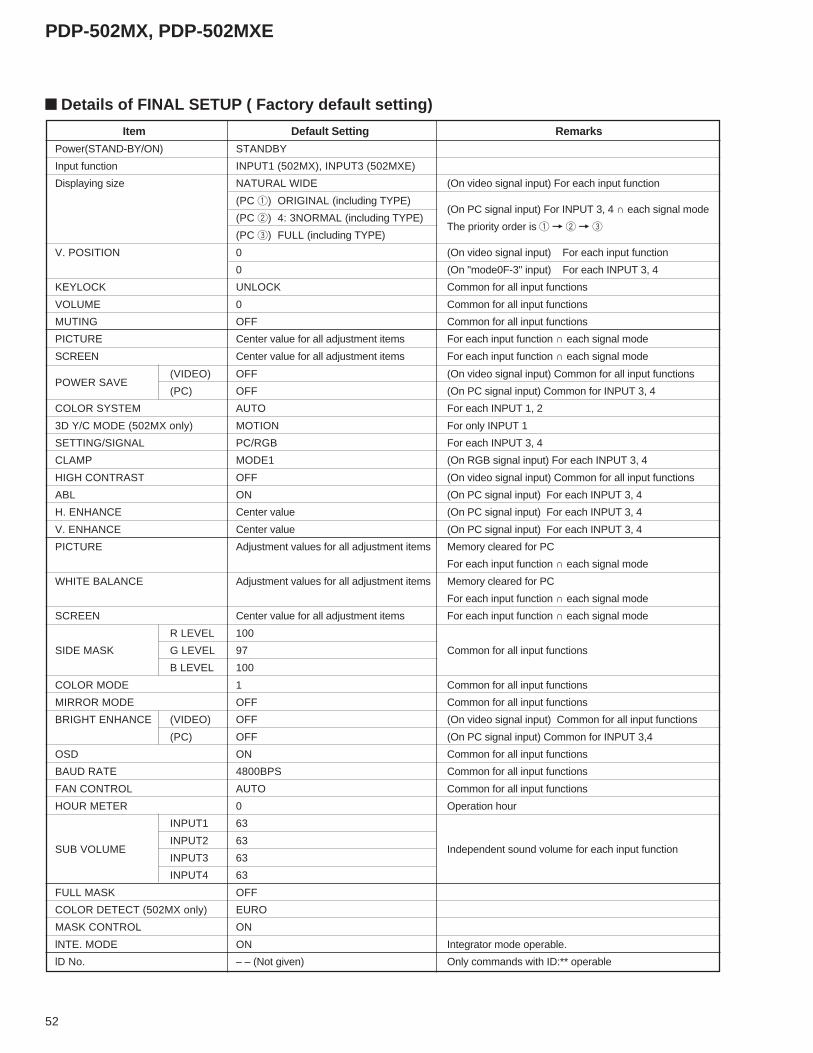
PDP-502MX, PDP-502MXE
52
Item Default Setting Remarks
Power(STAND-BY/ON) STANDBY
Input function INPUT1 (502MX), INPUT3 (502MXE)
Displaying size NATURAL WIDE (On video signal input) For each input function
(PC 1) ORIGINAL (including TYPE)(On PC signal input) For INPUT 3, 4 ∩ each signal mode
(PC 2) 4: 3NORMAL (including TYPE)The priority order is 1 = 2 = 3
(PC 3) FULL (including TYPE)
V. POSITION 0 (On video signal input) For each input function
0 (On "mode0F-3" input) For each INPUT 3, 4
KEYLOCK UNLOCK Common for all input functions
VOLUME 0 Common for all input functions
MUTING OFF Common for all input functions
PICTURE Center value for all adjustment items For each input function ∩ each signal mode
SCREEN Center value for all adjustment items For each input function ∩ each signal mode
(VIDEO) OFF (On video signal input) Common for all input functionsPOWER SAVE
(PC) OFF (On PC signal input) Common for INPUT 3, 4
COLOR SYSTEM AUTO For each INPUT 1, 2
3D Y/C MODE (502MX only) MOTION For only INPUT 1
SETTING/SIGNAL PC/RGB For each INPUT 3, 4
CLAMP MODE1 (On RGB signal input) For each INPUT 3, 4
HIGH CONTRAST OFF (On video signal input) Common for all input functions
ABL ON (On PC signal input) For each INPUT 3, 4
H. ENHANCE Center value (On PC signal input) For each INPUT 3, 4
V. ENHANCE Center value (On PC signal input) For each INPUT 3, 4
PICTURE Adjustment values for all adjustment items Memory cleared for PC
For each input function ∩ each signal mode
WHITE BALANCE Adjustment values for all adjustment items Memory cleared for PC
For each input function ∩ each signal mode
SCREEN Center value for all adjustment items For each input function ∩ each signal mode
R LEVEL 100
SIDE MASK G LEVEL 97 Common for all input functions
B LEVEL 100
COLOR MODE 1 Common for all input functions
MIRROR MODE OFF Common for all input functions
BRIGHT ENHANCE (VIDEO) OFF (On video signal input) Common for all input functions
(PC) OFF (On PC signal input) Common for INPUT 3,4
OSD ON Common for all input functions
BAUD RATE 4800BPS Common for all input functions
FAN CONTROL AUTO Common for all input functions
HOUR METER 0 Operation hour
INPUT1 63
INPUT2 63SUB VOLUME Independent sound volume for each input function
INPUT3 63
INPUT4 63
FULL MASK OFF
COLOR DETECT (502MX only) EURO
MASK CONTROL ON
lNTE. MODE ON Integrator mode operable.
lD No. – – (Not given) Only commands with ID:** operable
Details of FINAL SETUP ( Factory default setting)
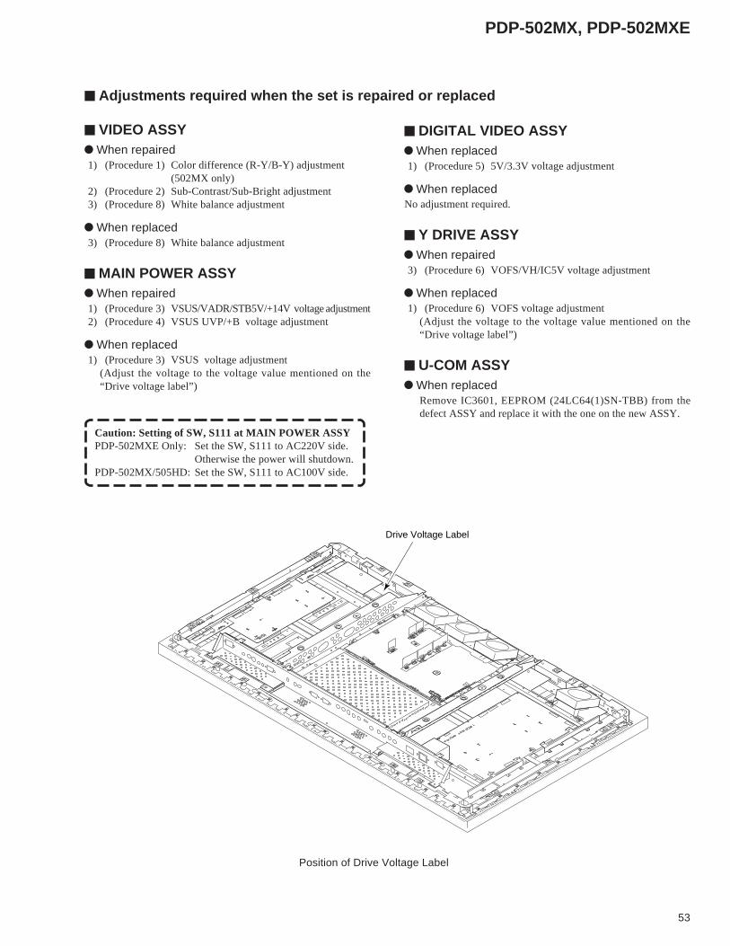
PDP-502MX, PDP-502MXE
53
Adjustments required when the set is repaired or replaced
VIDEO ASSY When repaired
1) (Procedure 1) Color difference (R-Y/B-Y) adjustment(502MX only)
2) (Procedure 2) Sub-Contrast/Sub-Bright adjustment3) (Procedure 8) White balance adjustment
When replaced3) (Procedure 8) White balance adjustment
MAIN POWER ASSY When repaired
1) (Procedure 3)VSUS/VADR/STB5V/+14V voltage adjustment2) (Procedure 4) VSUS UVP/+B voltage adjustment
When replaced1) (Procedure 3) VSUS voltage adjustment
(Adjust the voltage to the voltage value mentioned on the“Drive voltage label”)
Caution: Setting of SW, S111 at MAIN POWER ASSYPDP-502MXE Only: Set the SW, S111 to AC220V side.
Otherwise the power will shutdown.PDP-502MX/505HD: Set the SW, S111 to AC100V side.
DIGITAL VIDEO ASSY When replaced
1) (Procedure 5) 5V/3.3V voltage adjustment
When replacedNo adjustment required.
Y DRIVE ASSY When repaired
3) (Procedure 6) VOFS/VH/IC5V voltage adjustment
When replaced1) (Procedure 6) VOFS voltage adjustment
(Adjust the voltage to the voltage value mentioned on the“Drive voltage label”)
U-COM ASSY When replaced
Remove IC3601, EEPROM (24LC64(1)SN-TBB) from thedefect ASSY and replace it with the one on the new ASSY.
Position of Drive Voltage Label
Drive Voltage Label
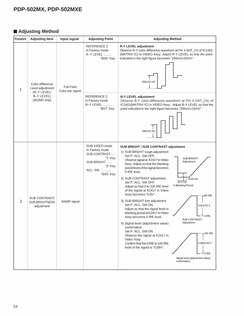
PDP-502MX, PDP-502MXE
54
Adjusting MethodProcedure Adjusting Item Input signal Adjusting Point Adjusting Method
SUB CONTRAST/SUB BRIGHTNESS
adjustment
SUB VIDEO modein Factory modeSUB CONTRAST.…. "1" KeySUB BRIGHT .…. "2" KeyACL. SW .…. .…. "BS5" Key
Color-differenceLevel adjustment
(R–Y LEVEL/B–Y LEVEL)(502MX only)
REFERENCE 2in Factory modeR–Y LEVEL ….…. "BS5" Key
Full FieldColor bar signal
R-Y LEVEL adjustmentObserve R-Y color-difference waveform at Pin 3 (INT_Cr) of IC1401(MATRIX IC) in VIDEO Assy. Adjust R-Y LEVEL so that the pointindicated in the right figure becomes "260mV±15mV".
260±15 mV
REFERENCE 2in Factory modeB–Y LEVEL ….…. "BS7" Key
B-Y LEVEL adjustmentObserve B-Y color-difference waveform at Pin 4 (INT_Cb) ofIC1401(MATRIX IC) in VIDEO Assy. Adjust B-Y LEVEL so that thepoint indicated in the right figure becomes "260mV±15mV".
260±15 mV
1) SUB BRIGHT rough adjustmentSet P. ACL. SW OFF.Observe signal at K2417 in VideoAssy. Adjust so that the blankingperiod level of the signal becomes0 IRE level.
2) SUB CONTRAST adjustmentSet P. ACL. SW OFF.Adjust so that 0 to 100 IRE levelof the signal at K2417 in VideoAssy becomes "0.8V".
3) SUB BRIGHT fine adjustmentSet P. ACL. SW ON.Adjust so that the signal level inblanking period at K2417 in VideoAssy becomes 0 IRE level.
4) Signal level (adjustment value)confirmationSet P. ACL. SW ON.Observe the signal at K2417 inVideo Assy .Confirm that the 0 IRE to 100 IRElevel of the signal is "0.58V".
RAMP signal
0±20 mV
SUB BRIGHTAdjustment
H Blanking Period
100 IRE
0 IRESUB CONTRASTAdjustment
0.8±0.02 V
100 IRE
0 IRE
0.58±0.05 V
Signal level (adjustment value)confirmation
1
2
SUB BRIGHT / SUB CONTRAST adjustment
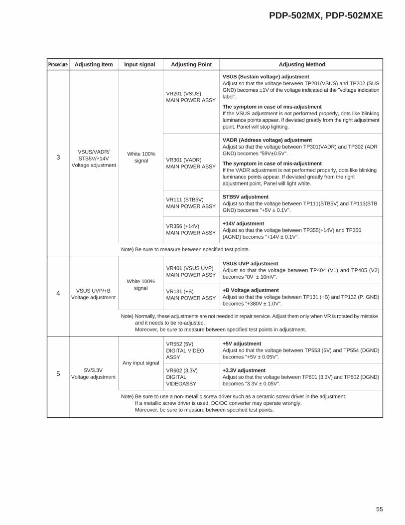
PDP-502MX, PDP-502MXE
55
Procedure Adjusting Item Input signal Adjusting Point Adjusting Method
VR201 (VSUS)MAIN POWER ASSY
VR301 (VADR)MAIN POWER ASSY
VR111 (STB5V)MAIN POWER ASSY
VR356 (+14V)MAIN POWER ASSY
VSUS (Sustain voltage) adjustmentAdjust so that the voltage between TP201(VSUS) and TP202 (SUSGND) becomes ±1V of the voltage indicated at the "voltage indicationlabel".
The symptom in case of mis-adjustmentIf the VSUS adjustment is not performed properly, dots like blinkingluminance points appear. If deviated greatly from the right adjustmentpoint, Panel will stop lighting.
VADR (Address voltage) adjustmentAdjust so that the voltage between TP301(VADR) and TP302 (ADRGND) becomes "59V±0.5V".
The symptom in case of mis-adjustmentIf the VADR adjustment is not performed properly, dots like blinkingluminance points appear. If deviated greatly from the rightadjustment point, Panel will light white.
STB5V adjustmentAdjust so that the voltage between TP111(STB5V) and TP113(STBGND) becomes "+5V ± 0.1V".
+14V adjustmentAdjust so that the voltage between TP355(+14V) and TP356(AGND) becomes "+14V ± 0.1V".
White 100%signal
VSUS/VADR/STB5V/+14V
Voltage adjustment
Note) Be sure to measure between specified test points.
VSUS UVP/+BVoltage adjustment
VR401 (VSUS UVP)MAIN POWER ASSY
VR131 (+B)MAIN POWER ASSY
VSUS UVP adjustmentAdjust so that the voltage between TP404 (V1) and TP405 (V2)becomes "0V ± 10mV".
+B Voltage adjustmentAdjust so that the voltage between TP131 (+B) and TP132 (P. GND)becomes "+380V ± 1.0V".
White 100%signal
Note) Normally, these adjustments are not needed in repair service. Adjust them only when VR is rotated by mistakeand it needs to be re-adjusted.Moreover, be sure to measure between specified test points in adjustment.
VR552 (5V)DIGITAL VIDEOASSY
VR602 (3.3V)DIGITALVIDEOASSY
+5V adjustmentAdjust so that the voltage between TP553 (5V) and TP554 (DGND)becomes "+5V ± 0.05V".
+3.3V adjustmentAdjust so that the voltage between TP601 (3.3V) and TP602 (DGND)becomes "3.3V ± 0.05V".
5V/3.3VVoltage adjustment
Note) Be sure to use a non-metallic screw driver such as a ceramic screw driver in the adjustment.If a metallic screw driver is used, DC/DC converter may operate wrongly.Moreover, be sure to measure between specified test points.
Any input signal
3
4
5
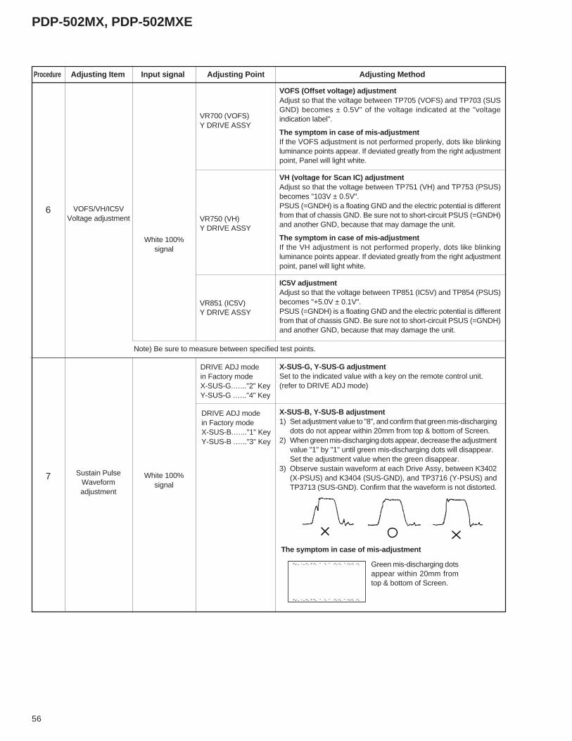
PDP-502MX, PDP-502MXE
56
DRIVE ADJ modein Factory modeX-SUS-G.…..."2" KeyY-SUS-G .….."4" Key
VR700 (VOFS)Y DRIVE ASSY
VR750 (VH)Y DRIVE ASSY
VR851 (IC5V)Y DRIVE ASSY
VOFS (Offset voltage) adjustmentAdjust so that the voltage between TP705 (VOFS) and TP703 (SUSGND) becomes ± 0.5V" of the voltage indicated at the "voltageindication label".
The symptom in case of mis-adjustmentIf the VOFS adjustment is not performed properly, dots like blinkingluminance points appear. If deviated greatly from the right adjustmentpoint, Panel will light white.
VH (voltage for Scan IC) adjustmentAdjust so that the voltage between TP751 (VH) and TP753 (PSUS)becomes "103V ± 0.5V".PSUS (=GNDH) is a floating GND and the electric potential is differentfrom that of chassis GND. Be sure not to short-circuit PSUS (=GNDH)and another GND, because that may damage the unit.
The symptom in case of mis-adjustmentIf the VH adjustment is not performed properly, dots like blinkingluminance points appear. If deviated greatly from the right adjustmentpoint, panel will light white.
IC5V adjustmentAdjust so that the voltage between TP851 (IC5V) and TP854 (PSUS)becomes "+5.0V ± 0.1V".PSUS (=GNDH) is a floating GND and the electric potential is differentfrom that of chassis GND. Be sure not to short-circuit PSUS (=GNDH)and another GND, because that may damage the unit.
White 100%signal
VOFS/VH/IC5VVoltage adjustment
Note) Be sure to measure between specified test points.
Sustain PulseWaveformadjustment
White 100%signal
X-SUS-G, Y-SUS-G adjustmentSet to the indicated value with a key on the remote control unit.(refer to DRIVE ADJ mode)
X-SUS-B, Y-SUS-B adjustment1) Set adjustment value to "8", and confirm that green mis-discharging
dots do not appear within 20mm from top & bottom of Screen.2) When green mis-discharging dots appear, decrease the adjustment
value "1" by "1" until green mis-discharging dots will disappear.Set the adjustment value when the green disappear.
3) Observe sustain waveform at each Drive Assy, between K3402(X-PSUS) and K3404 (SUS-GND), and TP3716 (Y-PSUS) andTP3713 (SUS-GND). Confirm that the waveform is not distorted.
6
7
Procedure Adjusting Item Input signal Adjusting Point Adjusting Method
DRIVE ADJ modein Factory modeX-SUS-B.…..."1" KeyY-SUS-B .….."3" Key
The symptom in case of mis-adjustment
Green mis-discharging dotsappear within 20mm fromtop & bottom of Screen.
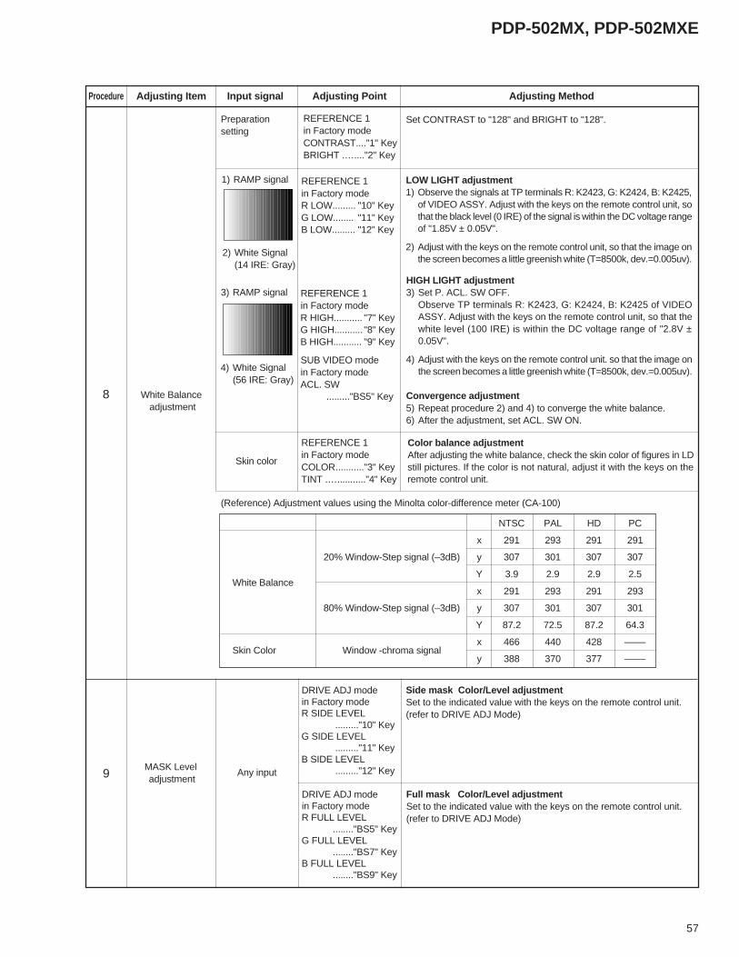
PDP-502MX, PDP-502MXE
57
NTSC PAL HD PC
x 291 293 291 291
20% Window-Step signal (–3dB) y 307 301 307 307
Y 3.9 2.9 2.9 2.5White Balance
x 291 293 291 293
80% Window-Step signal (–3dB) y 307 301 307 301
Y 87.2 72.5 87.2 64.3
x 466 440 428 ––––Skin Color Window -chroma signal
y 388 370 377 ––––
White Balance adjustment
1) RAMP signal REFERENCE 1in Factory modeR LOW......... "10" KeyG LOW........ "11" KeyB LOW......... "12" Key
LOW LIGHT adjustment1) Observe the signals at TP terminals R: K2423, G: K2424, B: K2425,
of VIDEO ASSY. Adjust with the keys on the remote control unit, sothat the black level (0 IRE) of the signal is within the DC voltage rangeof "1.85V ± 0.05V".
2) Adjust with the keys on the remote control unit, so that the image onthe screen becomes a little greenish white (T=8500k, dev.=0.005uv).
2) White Signal(14 IRE: Gray)
3) RAMP signal REFERENCE 1in Factory modeR HIGH........... "7" KeyG HIGH........... "8" KeyB HIGH........... "9" Key
SUB VIDEO modein Factory modeACL. SW ........."BS5" Key
HIGH LIGHT adjustment3) Set P. ACL. SW OFF.
Observe TP terminals R: K2423, G: K2424, B: K2425 of VIDEOASSY. Adjust with the keys on the remote control unit, so that thewhite level (100 IRE) is within the DC voltage range of "2.8V ±0.05V".
4) Adjust with the keys on the remote control unit. so that the image onthe screen becomes a little greenish white (T=8500k, dev.=0.005uv).
Convergence adjustment5) Repeat procedure 2) and 4) to converge the white balance.6) After the adjustment, set ACL. SW ON.
4) White Signal(56 IRE: Gray)
(Reference) Adjustment values using the Minolta color-difference meter (CA-100)
Set CONTRAST to "128" and BRIGHT to "128".
Skin color
REFERENCE 1in Factory modeCOLOR..........."3" KeyTINT .…..........."4" Key
Color balance adjustmentAfter adjusting the white balance, check the skin color of figures in LDstill pictures. If the color is not natural, adjust it with the keys on theremote control unit.
Preparationsetting
8
Procedure Adjusting Item Input signal Adjusting Point Adjusting Method
REFERENCE 1in Factory modeCONTRAST...."1" KeyBRIGHT .…...."2" Key
DRIVE ADJ modein Factory modeR FULL LEVEL ........"BS5" KeyG FULL LEVEL ........"BS7" KeyB FULL LEVEL ........"BS9" Key
Full mask Color/Level adjustmentSet to the indicated value with the keys on the remote control unit.(refer to DRIVE ADJ Mode)
MASK Level adjustment
DRIVE ADJ modein Factory modeR SIDE LEVEL ........."10" KeyG SIDE LEVEL ........."11" KeyB SIDE LEVEL ........."12" Key
Side mask Color/Level adjustmentSet to the indicated value with the keys on the remote control unit.(refer to DRIVE ADJ Mode)
Any input9
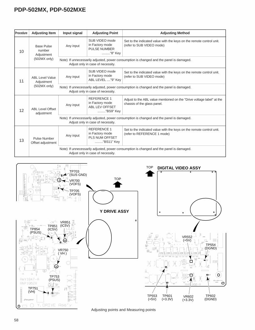
PDP-502MX, PDP-502MXE
58
Base Pulsenumber
Adjustment(502MX only)
Adjusting points and Measuring points
10
Procedure Adjusting Item Input signal Adjusting Point Adjusting Method
Any input
SUB VIDEO modein Factory modePULSE NUMBER ........."8" Key
Note) If unnecessarily adjusted, power consumption is changed and the panel is damaged.Adjust only in case of necessity.
Set to the indicated value with the keys on the remote control unit.(refer to SUB VIDEO mode)
ABL Level ValueAdjustment
(502MX only)11
Any input
SUB VIDEO modein Factory modeABL LEVEL ...."9" Key
Note) If unnecessarily adjusted, power consumption is changed and the panel is damaged.Adjust only in case of necessity.
Set to the indicated value with the keys on the remote control unit.(refer to SUB VIDEO mode)
ABL Level Offsetadjustment
12Any input
REFERENCE 1in Factory modeABL LEV OFFSET ........."BS9" Key
Note) If unnecessarily adjusted, power consumption is changed and the panel is damaged.Adjust only in case of necessity.
Adjust to the ABL value mentioned on the "Drive voltage label" at thechassis of the glass panel.
Pulse NumberOffset adjustment
13Any input
REFERENCE 1in Factory modePLS NUM OFFSET ........."BS11" Key
Note) If unnecessarily adjusted, power consumption is changed and the panel is damaged.Adjust only in case of necessity.
Set to the indicated value with the keys on the remote control unit.(refer to REFERENCE 1 mode)
VR602(+3.3V)
VR552(+5V)
TP554(DGND)
TP602(DGND)
TP601(+3.3V)
TP553(+5V)
DIGITAL VIDEO ASSYTOPTP703(SUS GND)
VR700(VOFS)
TP705(VOFS)
Y DRIVE ASSY
TOP
VR851(IC5V)
TP854(PSUS)
TP851(IC5V)
TP751(VH)
TP753(PSUS)
VR750( VH )
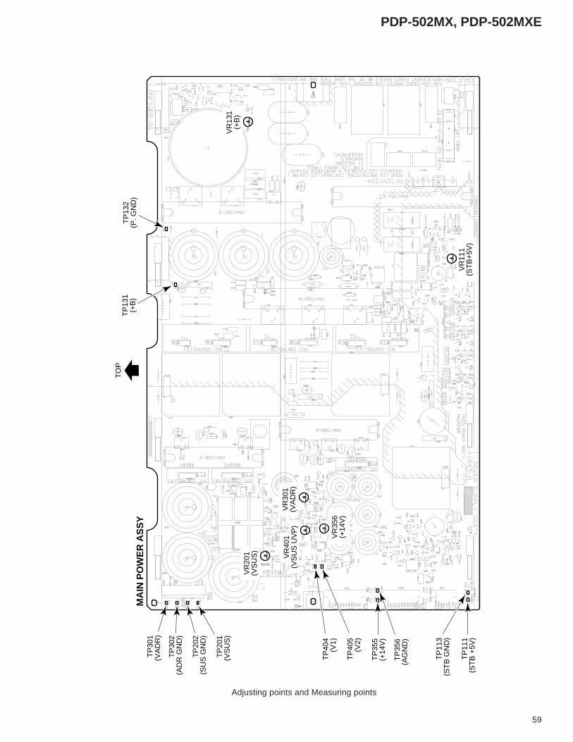
PDP-502MX, PDP-502MXE
59
Adjusting points and Measuring points
TO
P
TP
301
(VA
DR
)
TP
302
(AD
R G
ND
)
TP
202
(SU
S G
ND
)
TP
201
(VS
US
)
TP
404
(V1)
TP
405
(V2)
TP
355
(+14
V)
TP
356
(AG
ND
)
TP
113
(ST
B G
ND
)
TP
111
(ST
B +
5V)
VR
201
(VS
US
)
VR
301
(VA
DR
)
VR
111
(ST
B+
5V)
VR
131
(+B
)
VR
356
(+14
V)
VR
401
(VS
US
UV
P)
TP
132
(P. G
ND
)T
P13
1(+
B)
MA
IN P
OW
ER
AS
SY
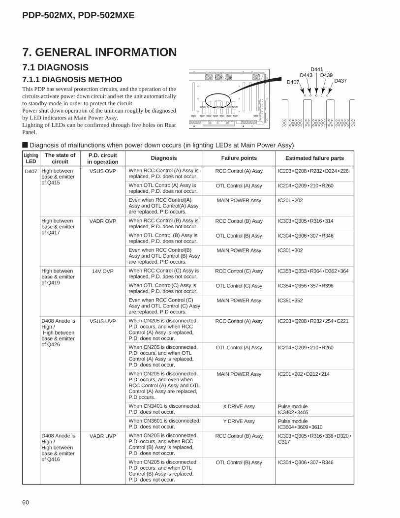
PDP-502MX, PDP-502MXE
60
IC203 • Q208 • R232 • D224 • 226
IC204 • Q209 • 210 • R260
IC201 • 202
IC303 • Q305 • R316 • 314
IC304 • Q306 • 307 • R346
IC301 • 302
IC353 • Q353 • R364 • D362 • 364
IC354 • Q356 • 357 • R396
IC351 • 352
IC203 • Q208 • R232 • 254 • C221
IC204 • Q209 • 210 • R260
IC201 • 202 • D212 • 214
Pulse moduleIC3402 • 3405
Pulse moduleIC3604 • 3609 • 3610
IC303 • Q305 • R316 • 338 • D320 •C317
IC304 • Q306 • 307 • R346
High betweenbase & emitterof Q415
High betweenbase & emitterof Q417
High betweenbase & emitterof Q419
D408 Anode isHigh / High betweenbase & emitterof Q426
D408 Anode isHigh /High betweenbase & emitterof Q416
VSUS OVP
VADR OVP
14V OVP
VSUS UVP
VADR UVP
When RCC Control (A) Assy isreplaced, P.D. does not occur.
When OTL Control(A) Assy isreplaced, P.D. does not occur.
Even when RCC Control(A)Assy and OTL Control(A) Assyare replaced, P.D occurs.
When RCC Control (B) Assy isreplaced, P.D. does not occur.
When OTL Control (B) Assy isreplaced, P.D. does not occur.
Even when RCC Control(B)Assy and OTL Control (B) Assyare replaced, P.D occurs.
When RCC Control (C) Assy isreplaced, P.D. does not occur.
When OTL Control(C) Assy isreplaced, P.D. does not occur.
Even when RCC Control (C)Assy and OTL Control (C) Assyare replaced, P.D occurs.
When CN205 is disconnected,P.D. occurs, and when RCCControl (A) Assy is replaced,P.D. does not occur.
When CN205 is disconnected,P.D. occurs, and when OTLControl (A) Assy is replaced,P.D. does not occur.
When CN205 is disconnected,P.D. occurs, and even whenRCC Control (A) Assy and OTLControl (A) Assy are replaced,P.D occurs.
When CN3401 is disconnected,P.D. does not occur.
When CN3601 is disconnected,P.D. does not occur.
When CN205 is disconnected,P.D. occurs, and when RCCControl (B) Assy is replaced,P.D. does not occur.
When CN205 is disconnected,P.D. occurs, and when OTLControl (B) Assy is replaced,P.D. does not occur.
RCC Control (A) Assy
OTL Control (A) Assy
MAIN POWER Assy
RCC Control (B) Assy
OTL Control (B) Assy
MAIN POWER Assy
RCC Control (C) Assy
OTL Control (C) Assy
MAIN POWER Assy
RCC Control (A) Assy
OTL Control (A) Assy
MAIN POWER Assy
X DRIVE Assy
Y DRIVE Assy
RCC Control (B) Assy
OTL Control (B) Assy
7.1 DIAGNOSIS
This PDP has several protection circuits, and the operation of thecircuits activate power down circuit and set the unit automaticallyto standby mode in order to protect the circuit.Power shut down operation of the unit can roughly be diagnosedby LED indicators at Main Power Assy.Lighting of LEDs can be confirmed through five holes on RearPanel.
7. GENERAL INFORMATIOND441
D439D437
D443D407
Diagnosis of malfunctions when power down occurs (in lighting LEDs at Main Power Assy)
D407
7.1.1 DIAGNOSIS METHOD
The state ofcircuit
P.D. circuitin operation
Diagnosis Failure points Estimated failure partsLightingLED
PDP-502MX, PDP-502MXE
61
D408 Anode isHigh/ Highbetween base &emitter of Q416
D408 Anode isHigh/ Highbetween base &emitter of Q418
D408 Anode isHigh/ Highbetween base &emitter of Q421
D408 Anode isHigh/ Highbetween base &emitter of Q420
D408 Anode isHigh/ Highbetween base &emitter of Q435
D405 Anode isHigh
High betweenbase & emitterof Q111
D852 Anode isHigh.
TP555 Hi
TP556 Hi
TP604 Hi
TP603 Hi
TP555 Lo
TP556 Lo
TP603 Lo
TP604 Lo
D4501 Anode is High.
D3457 Anode isHigh.
K706Hi
K705Hi
K754Hi
VADR UVP
14V UVP
12V UVP
8V UVP
–8V UVP
B OVP
AC200V P.D.
VF OVP
5V OVP
5V UVP
3.3V OVP
3.3V UVP
ICP OPEN
AUDIO P.D.
12V OCP
VOFS OVP
VOFS UVP
VH OVP
When CN205 is disconnected,P.D. occurs, and even whenRCC Control (B) Assy and OTLControl (B) Assy are replaced,P.D occurs.
When CN205 is disconnected,P.D. does not occur.
When CN306 & 354 aredisconnected, P.D. occurs.
When CN306 is disconnected,P.D. does not occur.
When CN354 is disconnected,P.D. does not occur.
When CN355 is disconnected,P.D. occurs.
When CN356 is disconnected,P.D. does not occur.
When CN306 is disconnected,P.D. occurs.
When CN306 is disconnected,P.D. does not occur.
When CN306 is disconnected,P.D. occurs.
When CN306 is disconnected,P.D. does not occur.
AC power input is appropriate.
When the power supply isturned on, a part of the screenshines in white momentarily andP.D. occurs.
Drive section (drive controlsignals & drive signal outputelements) in normal operation.
VOFS D/D Conv. Block innormal operation
MAIN POWER Assy
CABLE Assy
MAIN POWER Assy14V D/D CONV. BLOCK
ANALOG VIDEO Assy
Y DRIVE AssyIC5V D/D CONV. BLOCK
MAIN POWER Assy12V D/D CONV. BLOCK
DIGITAL VIDEO AssyD/D CONV. BLOCK
MAIN POWER Assy8V D/D CONV. BLOCK
ANALOG VIDEO Assy
MAIN POWER Assy–8V D/D CONV. BLOCK
ANALOG VIDEO Assy
MAIN POWER AssyPFC BLOCK
MAIN POWER AssySTB BLOCK
Y DRIVE Assy
DIGITAL VIDEO Assy5V D/D CONV.BLOCK
DIGITAL VIDEO Assy3.3V D/D CONV. BLOCK
CABLE AssyRESONATOR BLOCK
Address Module
DIGITAL VIDEO AssyDIGITAL BLOCK
AUDIO Assy
X DRIVE AssyPulse Module
X DRIVE AssyRESET DRIVE BLOCK
Y DRIVE AssyVOFS D/D CONV. BLOCK
Y DRIVE AssyVOFS D/D CONV. BLOCK
Y DRIVE AssySUS_MSK BLOCK
Y DRIVE AssyVH D/D CONV. BLOCK
IC301 • 302 • Q302
RCC Control (C) Assy • OTLControl (C) Assy • IC351 • 352
IC852
RCC Control (C) Assy • OTLControl (C) Assy • IC351 • 352IC551 • 601 • Q554 • 555 • 604 • 605
RCC Control (C) Assy • OTLControl (C) Assy • IC351 • 352
RCC Control (C) Assy • OTLControl (C) Assy • IC351 • 352 •D373
IC131
IC111 • 112 • 113 • T111
IC852 • 853 • 854
IC551
IC601
IC1008 • Q1001–Q1006
UPD16340 (IC??????)
IC2201
IC4502 • C4520 • 4522
Pulse moduleIC3402 • 3405
Q3401 • 3402 • 3403
IC702 • 704
IC701 • 702 • 704
R3717 • 3730
IC751 • 752
D407
D407•
D443
D407•
D441
D407•
D439
The state ofcircuit
P.D. circuitin operation
Diagnosis Failure points Estimated failure partsLightingLED
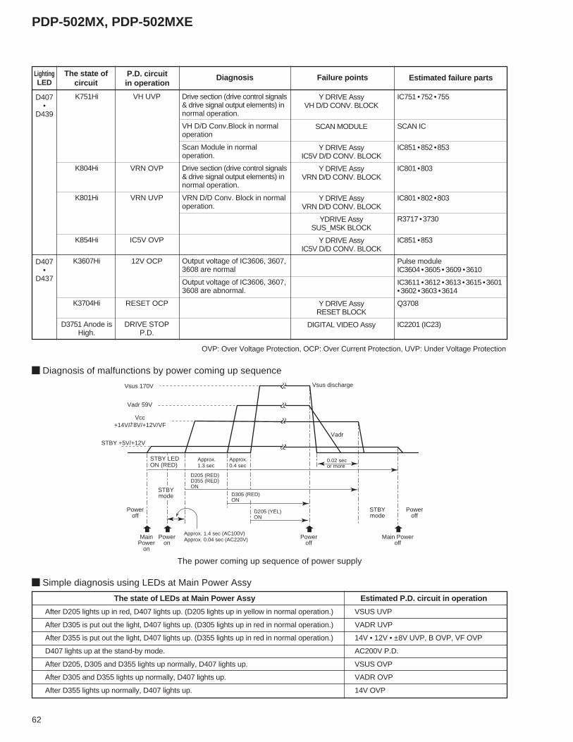
PDP-502MX, PDP-502MXE
62
K751Hi
K804Hi
K801Hi
K854Hi
K3607Hi
K3704Hi
D3751 Anode isHigh.
VH UVP
VRN OVP
VRN UVP
IC5V OVP
12V OCP
RESET OCP
DRIVE STOPP.D.
Drive section (drive control signals& drive signal output elements) innormal operation.
VH D/D Conv.Block in normaloperation
Scan Module in normaloperation.
Drive section (drive control signals& drive signal output elements) innormal operation.
VRN D/D Conv. Block in normaloperation.
Output voltage of IC3606, 3607,3608 are normal
Output voltage of IC3606, 3607,3608 are abnormal.
Y DRIVE AssyVH D/D CONV. BLOCK
SCAN MODULE
Y DRIVE AssyIC5V D/D CONV. BLOCK
Y DRIVE AssyVRN D/D CONV. BLOCK
Y DRIVE AssyVRN D/D CONV. BLOCK
YDRIVE AssySUS_MSK BLOCK
Y DRIVE AssyIC5V D/D CONV. BLOCK
Y DRIVE AssyRESET BLOCK
DIGITAL VIDEO Assy
IC751 • 752 • 755
SCAN IC
IC851 • 852 • 853
IC801 • 803
IC801 • 802 • 803
R3717 • 3730
IC851 • 853
Pulse moduleIC3604 • 3605 • 3609 • 3610
IC3611 • 3612 • 3613 • 3615 • 3601• 3602 • 3603 • 3614
Q3708
IC2201 (IC23)
D407•
D439
D407•
D437
The state ofcircuit
P.D. circuitin operation
Diagnosis Failure points Estimated failure partsLightingLED
OVP: Over Voltage Protection, OCP: Over Current Protection, UVP: Under Voltage Protection
Diagnosis of malfunctions by power coming up sequence
Vsus 170V
Vadr 59V
Vcc+14V/+8V/+12V/VF
STBY +5V/+12V
Approx.1.3 sec
Approx. 1.4 sec (AC100V)Approx. 0.04 sec (AC220V)
Approx.0.4 sec
0.02 secor more
Vsus discharge
Vadr
STBY LEDON (RED)
D205 (RED)D355 (RED)ON
D305 (RED)ON
D205 (YEL)ON
Main Poweroff
Poweroff
Poweroff
MainPower
on
Poweron
STBYmode
STBYmode
Poweroff
The power coming up sequence of power supply
Simple diagnosis using LEDs at Main Power Assy
The state of LEDs at Main Power Assy Estimated P.D. circuit in operation
After D205 lights up in red, D407 lights up. (D205 lights up in yellow in normal operation.) VSUS UVP
After D305 is put out the light, D407 lights up. (D305 lights up in red in normal operation.) VADR UVP
After D355 is put out the light, D407 lights up. (D355 lights up in red in normal operation.) 14V • 12V • ±8V UVP, B OVP, VF OVP
D407 lights up at the stand-by mode. AC200V P.D.
After D205, D305 and D355 lights up normally, D407 lights up. VSUS OVP
After D305 and D355 lights up normally, D407 lights up. VADR OVP
After D355 lights up normally, D407 lights up. 14V OVP
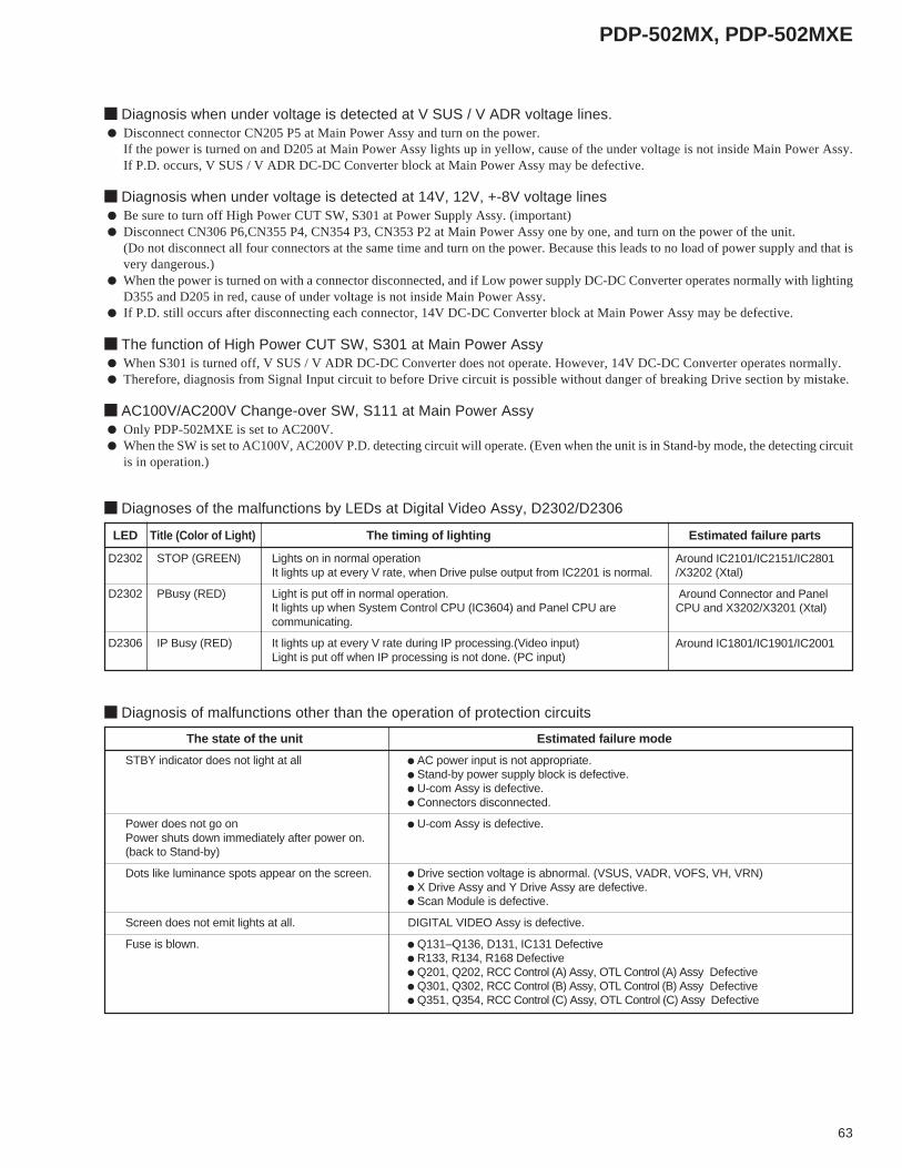
PDP-502MX, PDP-502MXE
63
D2302 STOP (GREEN) Lights on in normal operationIt lights up at every V rate, when Drive pulse output from IC2201 is normal.
D2302 PBusy (RED) Light is put off in normal operation.It lights up when System Control CPU (IC3604) and Panel CPU arecommunicating.
D2306 IP Busy (RED) It lights up at every V rate during IP processing.(Video input)Light is put off when IP processing is not done. (PC input)
The state of the unit Estimated failure mode
STBY indicator does not light at all AC power input is not appropriate. Stand-by power supply block is defective. U-com Assy is defective. Connectors disconnected.
Power does not go on U-com Assy is defective.Power shuts down immediately after power on.(back to Stand-by)
Dots like luminance spots appear on the screen. Drive section voltage is abnormal. (VSUS, VADR, VOFS, VH, VRN) X Drive Assy and Y Drive Assy are defective. Scan Module is defective.
Screen does not emit lights at all. DIGITAL VIDEO Assy is defective.
Fuse is blown. Q131–Q136, D131, IC131 Defective R133, R134, R168 Defective Q201, Q202, RCC Control (A) Assy, OTL Control (A) Assy Defective Q301, Q302, RCC Control (B) Assy, OTL Control (B) Assy Defective Q351, Q354, RCC Control (C) Assy, OTL Control (C) Assy Defective
Diagnosis of malfunctions other than the operation of protection circuits
Around IC2101/IC2151/IC2801/X3202 (Xtal)
Around Connector and PanelCPU and X3202/X3201 (Xtal)
Around IC1801/IC1901/IC2001
Diagnoses of the malfunctions by LEDs at Digital Video Assy, D2302/D2306
LED Title (Color of Light) The timing of lighting Estimated failure parts
Diagnosis when under voltage is detected at V SUS / V ADR voltage lines. Disconnect connector CN205 P5 at Main Power Assy and turn on the power.
If the power is turned on and D205 at Main Power Assy lights up in yellow, cause of the under voltage is not inside Main Power Assy.If P.D. occurs, V SUS / V ADR DC-DC Converter block at Main Power Assy may be defective.
Diagnosis when under voltage is detected at 14V, 12V, +-8V voltage lines Be sure to turn off High Power CUT SW, S301 at Power Supply Assy. (important) Disconnect CN306 P6,CN355 P4, CN354 P3, CN353 P2 at Main Power Assy one by one, and turn on the power of the unit.
(Do not disconnect all four connectors at the same time and turn on the power. Because this leads to no load of power supply and that isvery dangerous.)
When the power is turned on with a connector disconnected, and if Low power supply DC-DC Converter operates normally with lightingD355 and D205 in red, cause of under voltage is not inside Main Power Assy.
If P.D. still occurs after disconnecting each connector, 14V DC-DC Converter block at Main Power Assy may be defective.
The function of High Power CUT SW, S301 at Main Power Assy When S301 is turned off, V SUS / V ADR DC-DC Converter does not operate. However, 14V DC-DC Converter operates normally. Therefore, diagnosis from Signal Input circuit to before Drive circuit is possible without danger of breaking Drive section by mistake.
AC100V/AC200V Change-over SW, S111 at Main Power Assy Only PDP-502MXE is set to AC200V. When the SW is set to AC100V, AC200V P.D. detecting circuit will operate. (Even when the unit is in Stand-by mode, the detecting circuit
is in operation.)
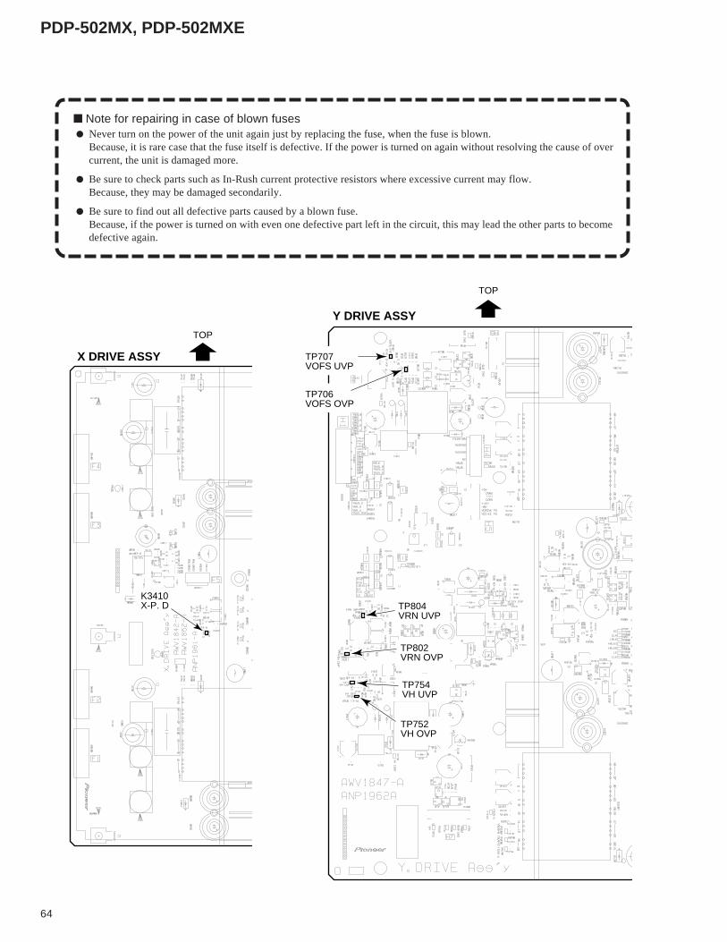
PDP-502MX, PDP-502MXE
64
Note for repairing in case of blown fuses Never turn on the power of the unit again just by replacing the fuse, when the fuse is blown.
Because, it is rare case that the fuse itself is defective. If the power is turned on again without resolving the cause of overcurrent, the unit is damaged more.
Be sure to check parts such as In-Rush current protective resistors where excessive current may flow.Because, they may be damaged secondarily.
Be sure to find out all defective parts caused by a blown fuse.Because, if the power is turned on with even one defective part left in the circuit, this may lead the other parts to becomedefective again.
X DRIVE ASSY
TOP
K3410X-P. D
Y DRIVE ASSY
TOP
TP707VOFS UVP
TP706VOFS OVP
TP804VRN UVP
TP802VRN OVP
TP754VH UVP
TP752VH OVP
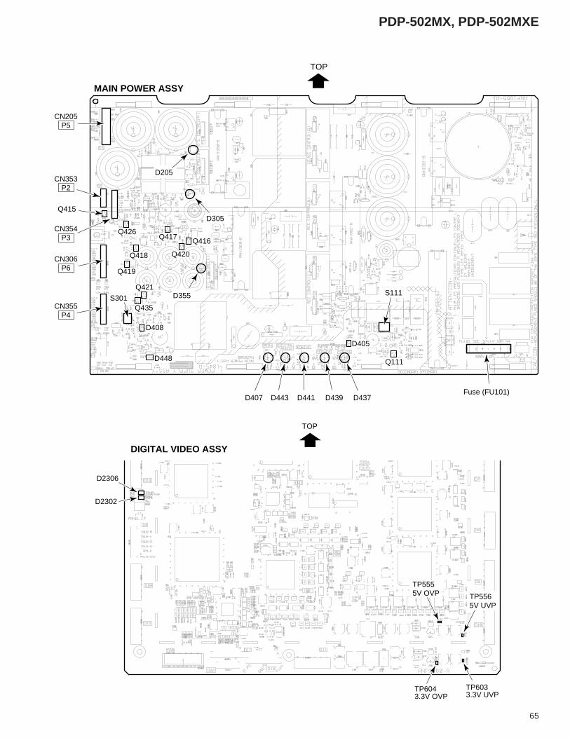
PDP-502MX, PDP-502MXE
65
TOP
MAIN POWER ASSY
D441 D439 D437D443D407
CN353P2
D205
D305
Fuse (FU101)
CN354P3
CN205P5
D355S301
Q419
Q435
D408
D448
Q421
Q418
Q426Q417
Q420
Q416
Q415
CN306P6
CN355P4
S111
Q111
D405
TP6033.3V UVP
TP6043.3V OVP
TP5555V OVP TP556
5V UVP
D2306
D2302
DIGITAL VIDEO ASSY
TOP
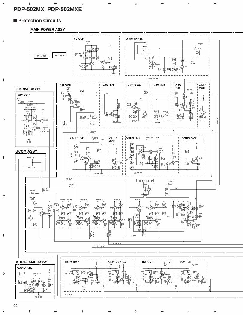
PDP-502MX, PDP-502MXE
66
A
B
C
D
1 2 3 4
1 2 3 4
Protection Circuits
X DRIVE ASSY
MAIN POWER ASSY
AUDIO AMP ASSY
UCOM ASSY
+12V OCP
AUDIO P.D.
+3.3V OVP +3.3V UVP +5V OVP +5V UVP
VSUS OVPVSUS UVPVADROVP
VADR UVP
VF OVP +8V UVP
AC200V P.D.+B OVP
–8V UVP +14VUVP
+14VOVP
+12V UVP
R3438
R3439
R34
40R
3442
R34
43R
3444
C34
25
47/1
610
k
10k
2.2k
10k
5.6k5.6k
R3437
C3424
Q3406 Q3405
D3408
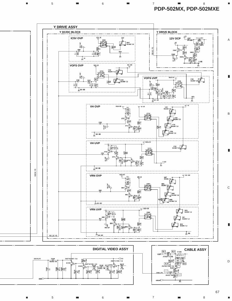
PDP-502MX, PDP-502MXE
67
A
B
C
D
5 6 7 8
5 6 7 8
DIGITAL VIDEO ASSY CABLE ASSY
Y DRIVE ASSY
VRN UVP
VRN OVP
VH UVP
VH OVP
IC5V OVP 12V OCP
Y DC/DC BLOCK Y DRIVE BLOCK
VOFS OVP
VOFS UVP
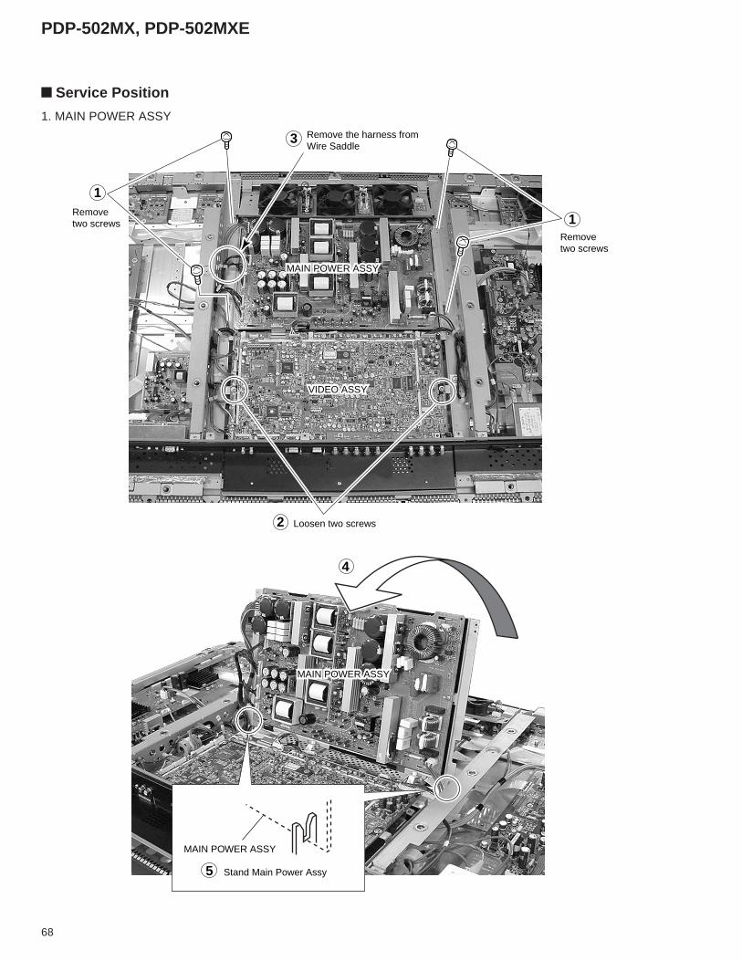
PDP-502MX, PDP-502MXE
68
Service Position
1. MAIN POWER ASSY
4
5
MAIN POWER ASSY
MAIN POWER ASSY
1
1
MAIN POWER ASSY
VIDEO ASSY
Stand Main Power Assy
3
2
Removetwo screws
Removetwo screws
Loosen two screws
Remove the harness fromWire Saddle
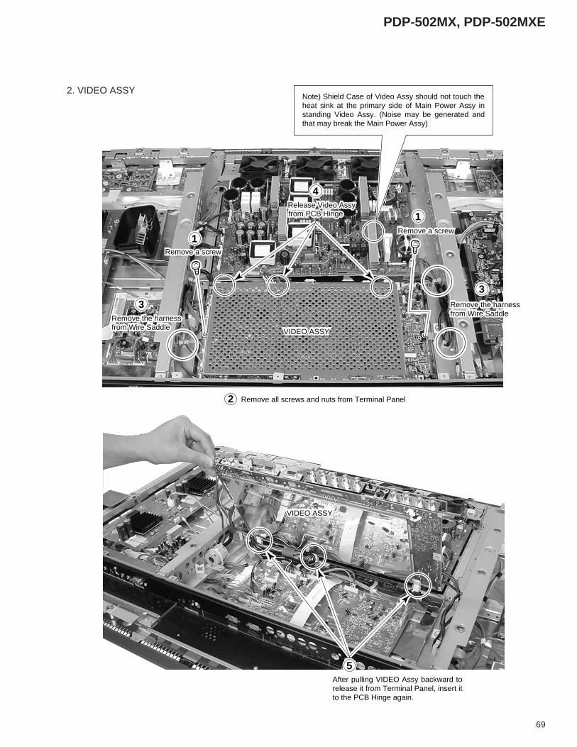
PDP-502MX, PDP-502MXE
69
2. VIDEO ASSY
1
VIDEO ASSY
4
33
1
VIDEO ASSY
5
Note) Shield Case of Video Assy should not touch the heat sink at the primary side of Main Power Assy in standing Video Assy. (Noise may be generated and that may break the Main Power Assy)
2 Remove all screws and nuts from Terminal Panel
Remove a screw
Remove a screw
Remove the harnessfrom Wire Saddle
Remove the harnessfrom Wire Saddle
Release Video Assyfrom PCB Hinge
After pulling VIDEO Assy backward to release it from Terminal Panel, insert it to the PCB Hinge again.
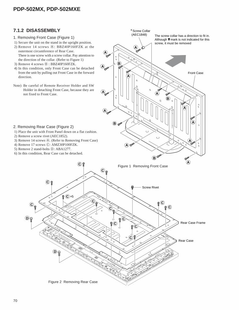
PDP-502MX, PDP-502MXE
70
D
D
CC
C
C
C
CC
C
C
C
C
C
C
×5
Screw Rivet
Rear Case Frame
Rear Case
A
A
A
A
A
A
A
A
A
AA
A
B
B
B
B
∗Screw Collar (AEC1848)
Front Case
The screw collar has a direction to fit in. Although mark is not indicated for this screw, it must be removed
7.1.2 DISASSEMBLY1. Removing Front Case (Figure 1) 1) Secure the unit on the stand in the upright position. 2) Remove 14 screws A : BBZ40P160FZK at the
outermost circumference of Rear Case.There is one screw with a screw collar. Pay attention tothe direction of the collar. (Refer to Figure 1)
3) Remove 4 screws B : BBZ40P160FZK. 4) In this condition, only Front Case can be detached
from the unit by pulling out Front Case in the forwarddirection.
Note) Be careful of Remote Receiver Holder and SWHolder in detaching Front Case, because they arenot fixed to Front Case.
Figure 1 Removing Front Case
2. Removing Rear Case (Figure 2) 1) Place the unit with Front Panel down on a flat cushion. 2) Remove a screw rivet (AEC1852). 3) Remove 14 screws A. (Refer to Removing Front Case) 4) Remove 17 screws C: AMZ30P100FZK. 5) Remove 2 stand-bolts D: ABA1277. 6) In this condition, Rear Case can be detached.
Figure 2 Removing Rear Case
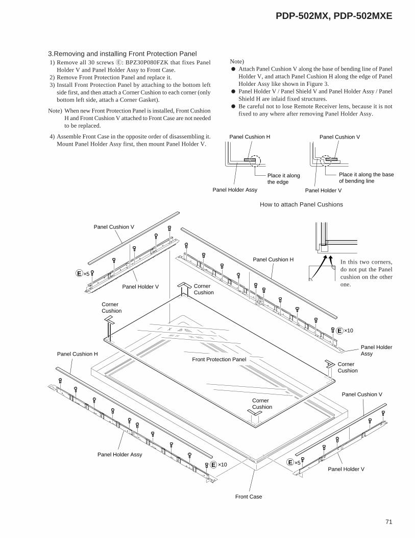
PDP-502MX, PDP-502MXE
71
E ×10
E ×10
E ×5
E ×5
Front Case
Panel Cushion V
Panel Cushion V
Panel Cushion H
Panel Cushion H
Panel Holder V
Panel Holder V
Panel Holder Assy
Panel HolderAssy
Front Protection Panel
CornerCushion
CornerCushion
CornerCushion
CornerCushion
3.Removing and installing Front Protection Panel 1) Remove all 30 screws E: BPZ30P080FZK that fixes Panel
Holder V and Panel Holder Assy to Front Case. 2) Remove Front Protection Panel and replace it. 3) Install Front Protection Panel by attaching to the bottom left
side first, and then attach a Corner Cushion to each corner (onlybottom left side, attach a Corner Gasket).
Note) When new Front Protection Panel is installed, Front CushionH and Front Cushion V attached to Front Case are not neededto be replaced.
4) Assemble Front Case in the opposite order of disassembling it.Mount Panel Holder Assy first, then mount Panel Holder V.
Note) Attach Panel Cushion V along the base of bending line of Panel
Holder V, and attach Panel Cushion H along the edge of PanelHolder Assy like shown in Figure 3.
Panel Holder V / Panel Shield V and Panel Holder Assy / PanelShield H are inlaid fixed structures.
Be careful not to lose Remote Receiver lens, because it is notfixed to any where after removing Panel Holder Assy.
How to attach Panel Cushions
In this two corners,do not put the Panelcushion on the otherone.
Panel Cushion H Panel Cushion V
Place it along the baseof bending line
Place it alongthe edge
Panel Holder Assy Panel Holder V
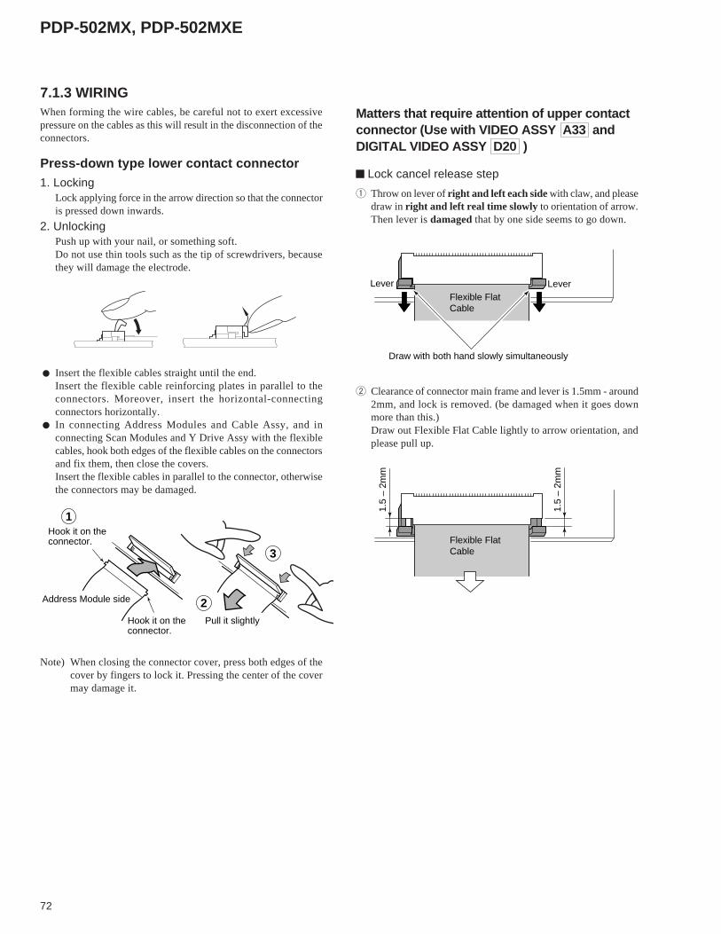
PDP-502MX, PDP-502MXE
72
Press-down type lower contact connector1. Locking
Lock applying force in the arrow direction so that the connectoris pressed down inwards.
2. UnlockingPush up with your nail, or something soft.Do not use thin tools such as the tip of screwdrivers, becausethey will damage the electrode.
7.1.3 WIRING
Insert the flexible cables straight until the end.Insert the flexible cable reinforcing plates in parallel to theconnectors. Moreover, insert the horizontal-connectingconnectors horizontally.
In connecting Address Modules and Cable Assy, and inconnecting Scan Modules and Y Drive Assy with the flexiblecables, hook both edges of the flexible cables on the connectorsand fix them, then close the covers.Insert the flexible cables in parallel to the connector, otherwisethe connectors may be damaged.
When forming the wire cables, be careful not to exert excessivepressure on the cables as this will result in the disconnection of theconnectors.
1
2
3
Hook it on theconnector.
Hook it on theconnector.
Address Module side
Pull it slightly
Note) When closing the connector cover, press both edges of thecover by fingers to lock it. Pressing the center of the covermay damage it.
2 Clearance of connector main frame and lever is 1.5mm - around2mm, and lock is removed. (be damaged when it goes downmore than this.)Draw out Flexible Flat Cable lightly to arrow orientation, andplease pull up.
Matters that require attention of upper contactconnector (Use with VIDEO ASSY A33 andDIGITAL VIDEO ASSY D20 )
Lock cancel release step
1 Throw on lever of right and left each side with claw, and pleasedraw in right and left real time slowly to orientation of arrow.Then lever is damaged that by one side seems to go down.
Flexible FlatCable
Draw with both hand slowly simultaneously
LeverLever
1.5
– 2m
m
1.5
– 2m
m
Flexible FlatCable
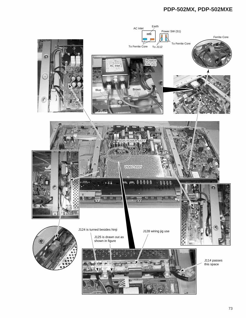
PDP-502MX, PDP-502MXE
73
VIDEO ASSYVIDEO ASSY
MAIN POWER ASSYMAIN POWER ASSY
AC InletAC Inlet
POWERSW (S1)POWERSW (S1)
To J112
Earth
To Ferrite CoreTo Ferrite Core
Ferrite Core
Blue Brown
Power SW (S1)AC Inlet
J114 passesthis space
J128 wiring jig useJ124 is turned besides hinji
J125 is drawn out asshown in figure
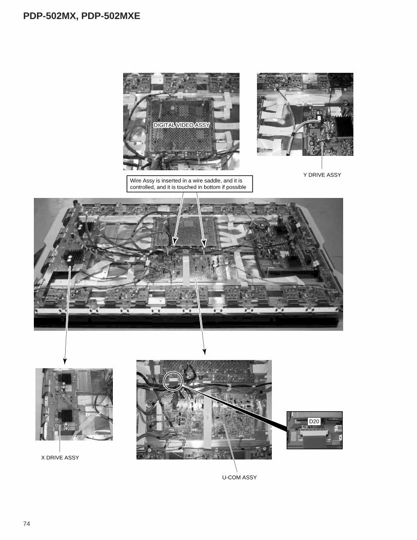
PDP-502MX, PDP-502MXE
74
X DRIVE ASSY
Y DRIVE ASSY
U-COM ASSY
DIGITAL VIDEO ASSYDIGITAL VIDEO ASSY
Wire Assy is inserted in a wire saddle, and it is controlled, and it is touched in bottom if possible
D20
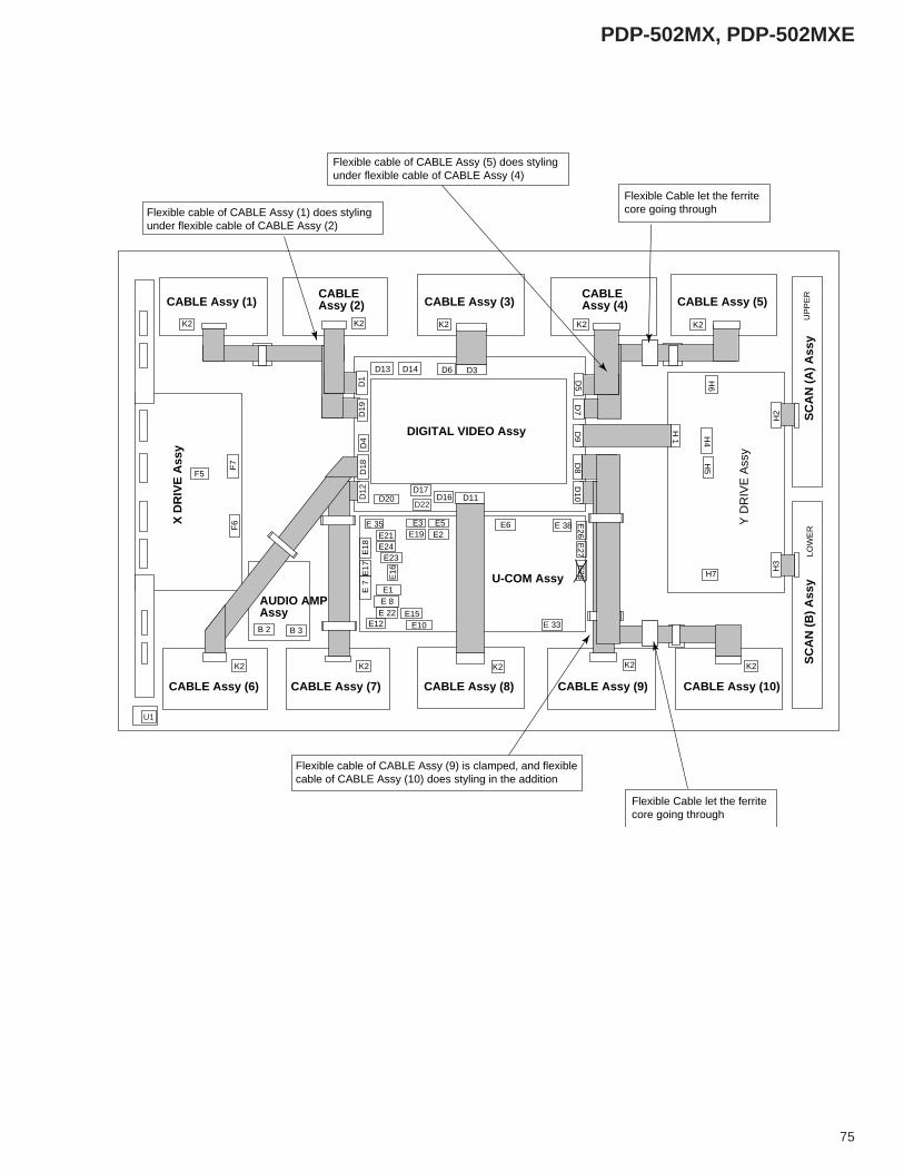
PDP-502MX, PDP-502MXE
75
K2
K2
H 1
H5
H7
H4
K2
H6
K2 K2
U1
D13 D14 D6 D3D
4
D11D16D17
D20
E23
E1
E12 E10
E 8
E3E 35E19 E2
E5
E21E24
E18
E 7
E17
K2
E6 E 38 E26
E28
E27
K2
F7
F6
F5
K2 K2 K2
D18
D7
D9
D8
D1
D19
UP
PE
RLO
WE
R
B 2 B 3E 33
E 22 E15
D22
D5
H3
H2
D12
D10
E16
X D
RIV
E A
ssy
Y D
RIV
E A
ssy
CABLE Assy (1)
CABLE Assy (6)
AUDIO AMPAssy
CABLE Assy (7) CABLE Assy (8)
DIGITAL VIDEO Assy
U-COM Assy
CABLE Assy (9) CABLE Assy (10)
SC
AN
(A
) A
ssy
SC
AN
(B
) A
ssy
CABLEAssy (2) CABLE Assy (3)
CABLEAssy (4) CABLE Assy (5)
Flexible cable of CABLE Assy (9) is clamped, and flexible cable of CABLE Assy (10) does styling in the addition
Flexible cable of CABLE Assy (1) does styling under flexible cable of CABLE Assy (2)
Flexible cable of CABLE Assy (5) does styling under flexible cable of CABLE Assy (4)
Flexible Cable let the ferrite core going through
Flexible Cable let the ferrite core going through
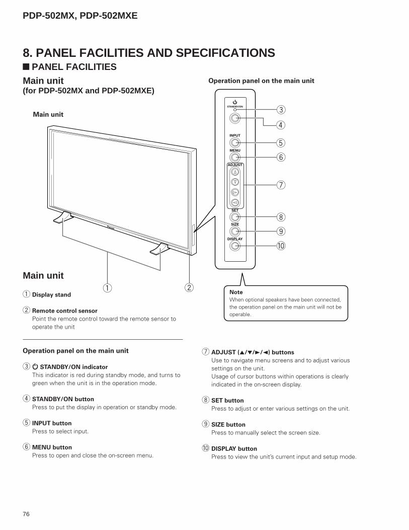
PDP-502MX, PDP-502MXE
76
2
4
5
6
7
8
9
0
3STANDBY/ON
INPUT
MENU
ADJUST
SET
SIZE
DISPLAY
1
8. PANEL FACILITIES AND SPECIFICATIONS PANEL FACILITIES
Main unit
1 Display stand
2 Remote control sensor
Point the remote control toward the remote sensor tooperate the unit
Operation panel on the main unit
3 STANDBY/ON indicator
This indicator is red during standby mode, and turns togreen when the unit is in the operation mode.
4 STANDBY/ON button
Press to put the display in operation or standby mode.
5 INPUT button
Press to select input.
6 MENU button
Press to open and close the on-screen menu.
7 ADJUST (5/∞/3/2) buttons
Use to navigate menu screens and to adjust varioussettings on the unit.Usage of cursor buttons within operations is clearlyindicated in the on-screen display.
8 SET button
Press to adjust or enter various settings on the unit.
9 SIZE button
Press to manually select the screen size.
0 DISPLAY button
Press to view the unit’s current input and setup mode.
Note
When optional speakers have been connected,the operation panel on the main unit will not beoperable.
Main unit
Operation panel on the main unitMain unit(for PDP-502MX and PDP-502MXE)
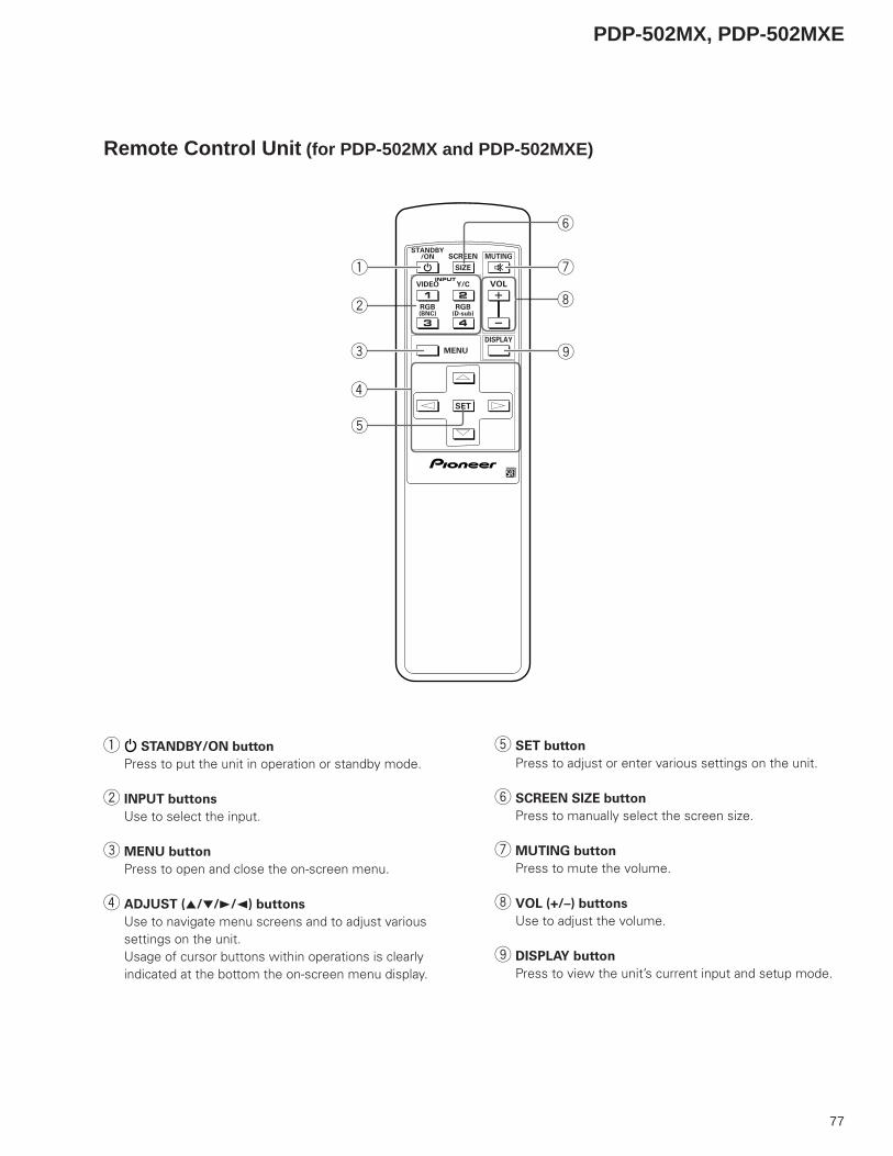
PDP-502MX, PDP-502MXE
77
Î
VIDEOINPUT
Y/C VOL
MENU
STANDBY/ON SCREEN MUTING
DISPLAY
RGB(D-sub)
SET
RGB(BNC)
1 2
3 4
SIZE
8
9
7
6
2
3
4
5
1
1 STANDBY/ON button
Press to put the unit in operation or standby mode.
2 INPUT buttons
Use to select the input.
3 MENU button
Press to open and close the on-screen menu.
4 ADJUST (5/∞/3/2) buttons
Use to navigate menu screens and to adjust varioussettings on the unit.Usage of cursor buttons within operations is clearlyindicated at the bottom the on-screen menu display.
5 SET button
Press to adjust or enter various settings on the unit.
6 SCREEN SIZE button
Press to manually select the screen size.
7 MUTING button
Press to mute the volume.
8 VOL (+/–) buttons
Use to adjust the volume.
9 DISPLAY button
Press to view the unit’s current input and setup mode.
Remote Control Unit (for PDP-502MX and PDP-502MXE)
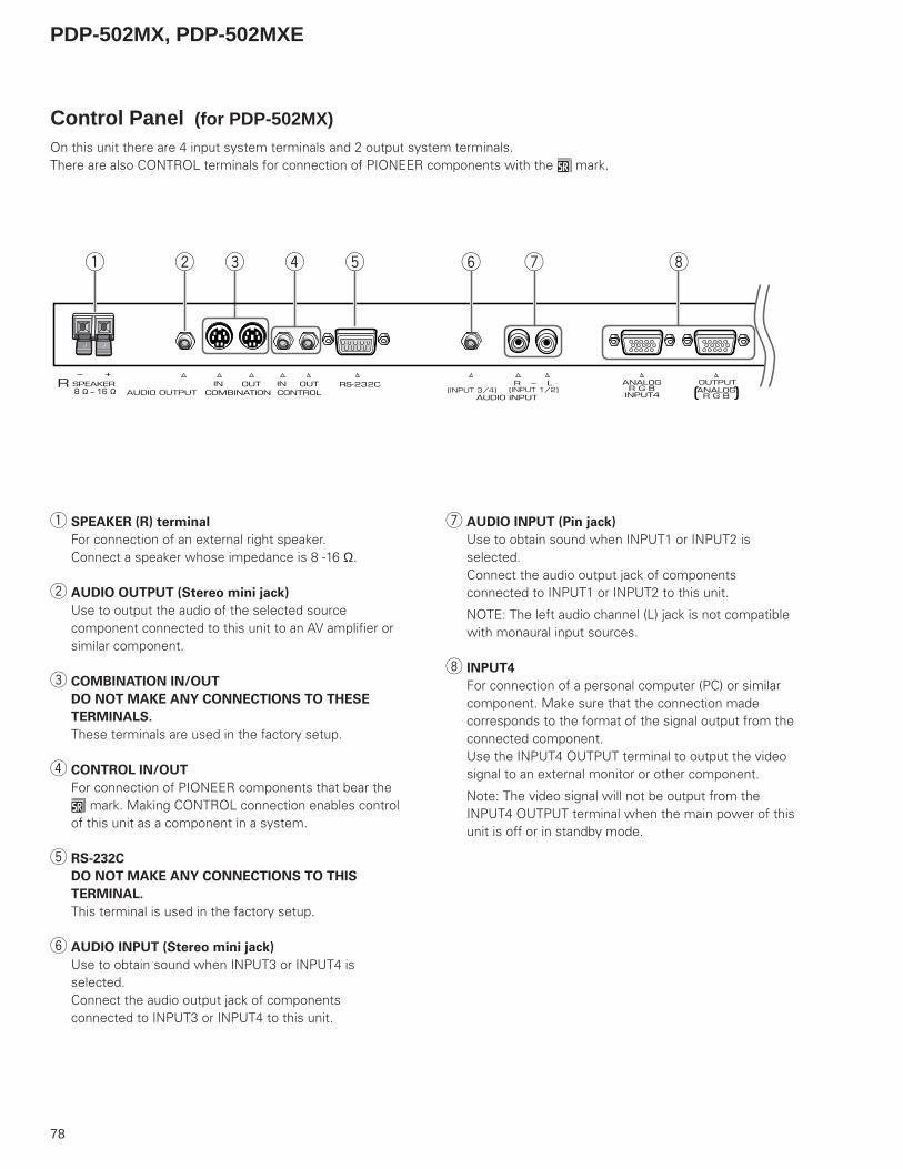
PDP-502MX, PDP-502MXE
78
Control Panel (for PDP-502MX)
1 2 3 4 5 6 7 8
SPEAKER
+–
CONTROLOUT
COMBINATIONIN
AUDIO OUTPUTINOUT RS-232C R – L ANALOG
R G B INPUT4
OUTPUT
AUDIO INPUT
ANALOGR G B( ((INPUT 1/2)(INPUT 3/4)8 Ω – 16 Ω
R
On this unit there are 4 input system terminals and 2 output system terminals.There are also CONTROL terminals for connection of PIONEER components with the Î mark.
1 SPEAKER (R) terminal
For connection of an external right speaker.Connect a speaker whose impedance is 8 -16 Ω.
2 AUDIO OUTPUT (Stereo mini jack)
Use to output the audio of the selected sourcecomponent connected to this unit to an AV amplifier orsimilar component.
3 COMBINATION IN/OUT
DO NOT MAKE ANY CONNECTIONS TO THESE
TERMINALS.
These terminals are used in the factory setup.
4 CONTROL IN/OUT
For connection of PIONEER components that bear theÎ mark. Making CONTROL connection enables controlof this unit as a component in a system.
5 RS-232C
DO NOT MAKE ANY CONNECTIONS TO THIS
TERMINAL.
This terminal is used in the factory setup.
6 AUDIO INPUT (Stereo mini jack)
Use to obtain sound when INPUT3 or INPUT4 isselected.Connect the audio output jack of componentsconnected to INPUT3 or INPUT4 to this unit.
7 AUDIO INPUT (Pin jack)
Use to obtain sound when INPUT1 or INPUT2 isselected.Connect the audio output jack of componentsconnected to INPUT1 or INPUT2 to this unit.
NOTE: The left audio channel (L) jack is not compatiblewith monaural input sources.
8 INPUT4
For connection of a personal computer (PC) or similarcomponent. Make sure that the connection madecorresponds to the format of the signal output from theconnected component.Use the INPUT4 OUTPUT terminal to output the videosignal to an external monitor or other component.
Note: The video signal will not be output from theINPUT4 OUTPUT terminal when the main power of thisunit is off or in standby mode.
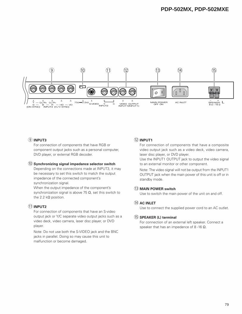
PDP-502MX, PDP-502MXE
79
INPUT3
YG B R
[ON SYNC] [H/V SYNC]INPUT2
CB/PB CR/PR 75Ωj2.2kΩ MAIN POWEROFF ON
AC INLET
9 0 - = ~ ! @
SPEAKER L+–
8 Ω – 16 ΩHD VD S-VIDEO VIDEOINPUT1
OUTPUT(INPUT1)
CY
9 INPUT3
For connection of components that have RGB orcomponent output jacks such as a personal computer,DVD player, or external RGB decoder.
0 Synchronizing signal impedance selector switch
Depending on the connections made at INPUT3, it maybe necessary to set this switch to match the outputimpedance of the connected component’ssynchronization signal.When the output impedance of the component’ssynchronization signal is above 75 Ω, set this switch tothe 2.2 kΩ position.
- INPUT2
For connection of components that have an S-videooutput jack or Y/C separate video output jacks such as avideo deck, video camera, laser disc player, or DVDplayer.
Note: Do not use both the S-VIDEO jack and the BNCjacks in parallel. Doing so may cause this unit tomalfunction or become damaged.
= INPUT1
For connection of components that have a compositevideo output jack such as a video deck, video camera,laser disc player, or DVD player.Use the INPUT1 OUTPUT jack to output the video signalto an external monitor or other component.
Note: The video signal will not be output from the INPUT1OUTPUT jack when the main power of this unit is off or instandby mode.
~ MAIN POWER switch
Use to switch the main power of the unit on and off.
! AC INLET
Use to connect the supplied power cord to an AC outlet.
@ SPEAKER (L) terminal
For connection of an external left speaker. Connect aspeaker that has an impedance of 8 -16 Ω.
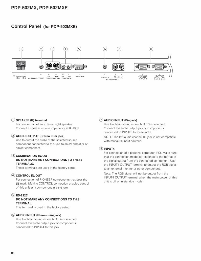
PDP-502MX, PDP-502MXE
80
Control Panel (for PDP-502MXE)
1 2 3 4 5 6 7 8
SPEAKER
+–
CONTROLOUT
COMBINATIONIN
AUDIO OUTPUTINOUT RS-232C R – L ANALOG
R G B INPUT4
OUTPUT
AUDIO INPUT
ANALOGR G B( ((INPUT 3)(INPUT 4)8 Ω – 16 Ω
R
1 SPEAKER (R) terminal
For connection of an external right speaker.Connect a speaker whose impedance is 8 -16 Ω.
2 AUDIO OUTPUT (Stereo mini jack)
Use to output the audio of the selected sourcecomponent connected to this unit to an AV amplifier orsimilar component.
3 COMBINATION IN/OUT
DO NOT MAKE ANY CONNECTIONS TO THESE
TERMINALS.
These terminals are used in the factory setup.
4 CONTROL IN/OUT
For connection of PIONEER components that bear theÎ mark. Making CONTROL connection enables controlof this unit as a component in a system.
5 RS-232C
DO NOT MAKE ANY CONNECTIONS TO THIS
TERMINAL.
This terminal is used in the factory setup.
6 AUDIO INPUT (Stereo mini jack)
Use to obtain sound when INPUT4 is selected.Connect the audio output jack of componentsconnected to INPUT4 to this jack.
7 AUDIO INPUT (Pin jack)
Use to obtain sound when INPUT3 is selected.Connect the audio output jack of componentsconnected to INPUT3 to these jacks.
NOTE: The left audio channel (L) jack is not compatiblewith monaural input sources.
8 INPUT4
For connection of a personal computer (PC). Make surethat the connection made corresponds to the format ofthe signal output from the connected component. Usethe INPUT4 OUTPUT terminal to output the RGB signalto an external monitor or other component.
Note: The RGB signal will not be output from theINPUT4 OUTPUT terminal when the main power of thisunit is off or in standby mode.
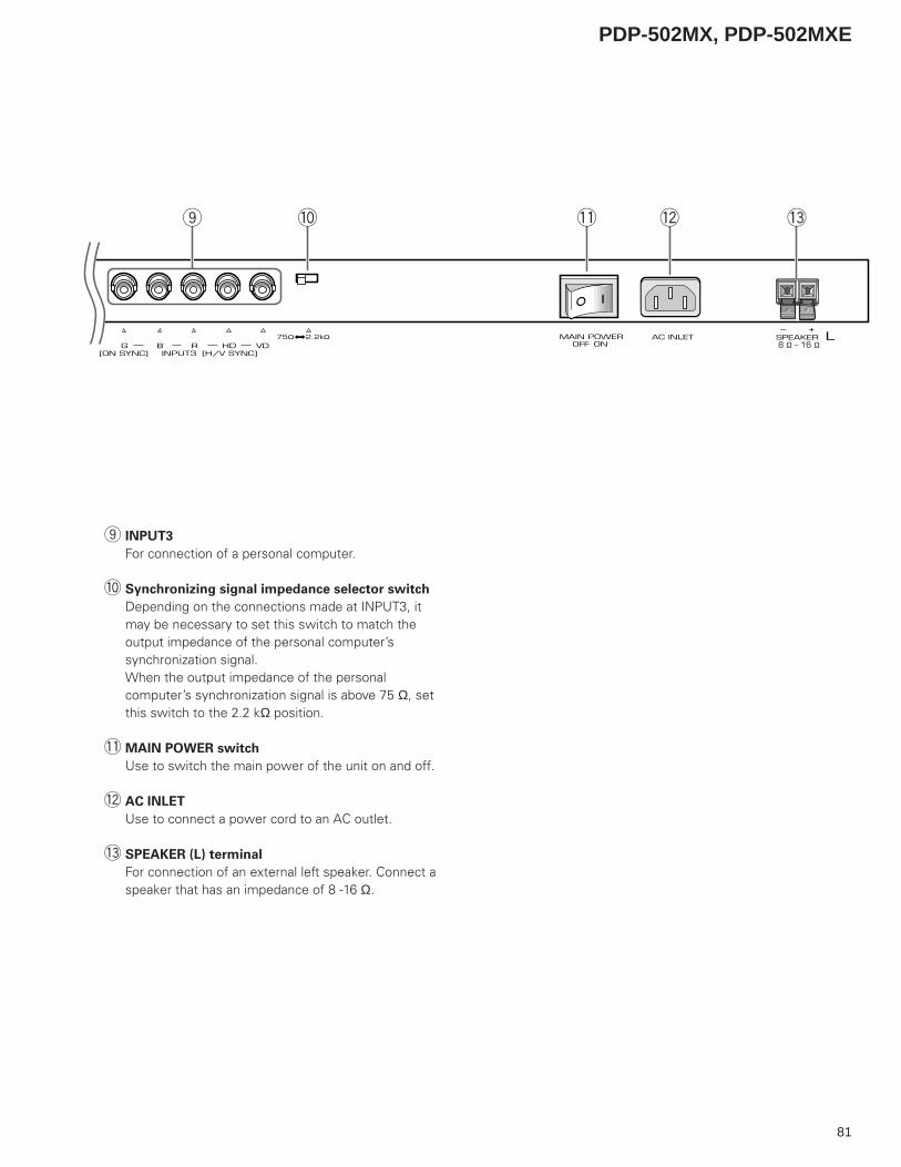
PDP-502MX, PDP-502MXE
81
INPUT3G B R
[ON SYNC] [H/V SYNC]
75Ωj2.2kΩ MAIN POWEROFF ON
AC INLET
9 0 - = ~
SPEAKER L+–
8 Ω – 16 ΩHD VD
9 INPUT3
For connection of a personal computer.
0 Synchronizing signal impedance selector switch
Depending on the connections made at INPUT3, itmay be necessary to set this switch to match theoutput impedance of the personal computer’ssynchronization signal.When the output impedance of the personalcomputer’s synchronization signal is above 75 Ω, setthis switch to the 2.2 kΩ position.
- MAIN POWER switch
Use to switch the main power of the unit on and off.
= AC INLET
Use to connect a power cord to an AC outlet.
~ SPEAKER (L) terminal
For connection of an external left speaker. Connect aspeaker that has an impedance of 8 -16 Ω.
PDP-502MX, PDP-502MXE
82
SPECIFICATIONS
GeneralLight emission panel ............ 50 inch plasma display panelNumber of pixels .............................................. 1280 x 768Power supply ............................. AC 100 - 120 V, 50/60 HzPower consumption ................................................ 470 WStandby power consumption ................................... 0.6 WExternal dimensions ........ 1218 (W) x 714 (H) x 98 (D) mm............................. 47-31/32 (W) x 28-1/8 (H) x 3-7/8 (D) in.
(when using table top stand)...................................... 1218 (W) x 737 (H) x 300 (D) mm..................... 47-31/32 (W) x 29-1/32 (H) x 11-13/16 (D) in.
Weight ............................................. 40.3 kg (88 lbs. 14 oz) (including table top stand) ................... 41 kg (90 lbs. 7 oz)Operating temperature range ..... 0 to 40 °C (32 to 104 °F)Operating atmospheric pressure range........................................ 0.8 to 1.1 atmospheric pressure
Input/output
Video
INPUT 1Input BNC jack
• Composite video signal 1 Vp-p/75 Ω/negative sync.
Output BNC jack75 Ω /with buffer
INPUT 2Input 1 S terminal (Mini DIN 4 pin)
2 BNC jack (x2)• Y/C saparate video signal (S2 compatible)Y . . . 1 Vp-p/75 Ω/negative sync.C . . . 0.286 Vp-p/75 Ω (NTSC)
0.3 Vp-p/75 Ω (PAL)
INPUT 3Input BNC jack (x5)
1 RGB signal (G ON SYNC compatible)RGB ... 0.7 Vp-p/75 Ω/no sync.HD/CS, VD ... TTL level
/positive and negative polarity/75 Ω or 2.2 kΩ(impedance switch)
G ON SYNC ...1 Vp-p/75 Ω/negative sync.
2 Component video signalY ... 1 Vp-p/75 Ω/negative sync.CB/PB, CR/PR
... 0.525 Vp-p/75 Ω(75% satulation level)
INPUT 4Input Mini D-sub 15 pin (socket connector)
1 RGB signal (G ON SYNC compatible)RGB ... 0.7 Vp-p/75 Ω/no sync.HD/CS, VD ... TTL level
/positive and negative polarity/2.2 kΩ
G ON SYNC... 1 Vp-p/75 Ω/negative sync.
*Compatible with Microsoft’s Plug & Play (VESA DDC1/2B)
2 Component video signal Y ... 1 Vp-p/75 Ω/negative sync. CB/PB, CR/PR
... 0.525 Vp-p/75 Ω(75% satulation level)
Output Mini D-sub 15 pin connector (socket)75 Ω/with buffer
Audio
Input AUDIO INPUT (for INPUT 1/2)Pin jack (x2)L/R ... 500mVrms/more than 10 kΩ
AUDIO INPUT (for INPUT 3/4)Stereo mini jackL/R ... 500mVrms/more than 10 kΩ
Output AUDIO OUTPUTStereo mini jackL/R ... 500mVrms (max)/less than 5 kΩ
SPEAKERL/R ... 8 – 16 Ω/2W +2W (at 8 Ω)
Control
RS-232C ... D-sub 9 pin (pin connector)COMBINATION IN/OUT
... Mini DIN 6 pin (x2)CONTROL IN/OUT ... monaural mini jack (x2)
AccessoriesPower cord ....................................................................... 1Pin/BNC conversion adaptor ............................................ 1Remote control unit ......................................................... 1Remote control unit case ................................................. 1AA (R6/UM-3) batteries .................................................... 2Cleaning cloth................................................................... 1Speed clamp .................................................................... 2Bead band ........................................................................ 2Warranty ........................................................................... 1Operations Instructions .................................................... 1Display stand .................................................................... 2Washer (large) .................................................................. 2Washer (small) ................................................................. 2Hex hole bolt (M8X40) ..................................................... 2
÷ Due to improvements, specifications and design are subject tochange without notice.
For PDP-502MX
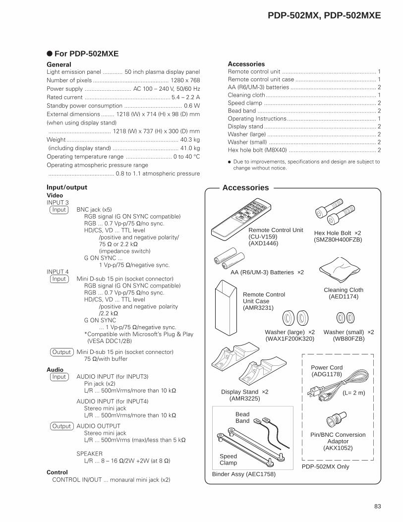
PDP-502MX, PDP-502MXE
83
GeneralLight emission panel ............ 50 inch plasma display panelNumber of pixels .............................................. 1280 x 768Power supply ............................ AC 100 – 240 V, 50/60 HzRated current .................................................... 5.4 – 2.2 AStandby power consumption ................................... 0.6 WExternal dimensions ........ 1218 (W) x 714 (H) x 98 (D) mm(when using display stand)...................................... 1218 (W) x 737 (H) x 300 (D) mm
Weight .................................................................... 40.3 kg (including display stand) ........................................ 41.0 kgOperating temperature range ............................ 0 to 40 °COperating atmospheric pressure range........................................ 0.8 to 1.1 atmospheric pressure
Input/output
Video
INPUT 3Input BNC jack (x5)
RGB signal (G ON SYNC compatible)RGB ... 0.7 Vp-p/75 Ω/no sync.HD/CS, VD ... TTL level
/positive and negative polarity/75 Ω or 2.2 kΩ(impedance switch)
G ON SYNC ...1 Vp-p/75 Ω/negative sync.
INPUT 4Input Mini D-sub 15 pin (socket connector)
RGB signal (G ON SYNC compatible)RGB ... 0.7 Vp-p/75 Ω/no sync.HD/CS, VD ... TTL level
/positive and negative polarity/2.2 kΩ
G ON SYNC... 1 Vp-p/75 Ω/negative sync.
*Compatible with Microsoft’s Plug & Play (VESA DDC1/2B)
Output Mini D-sub 15 pin (socket connector)75 Ω/with buffer
Audio
Input AUDIO INPUT (for INPUT3)Pin jack (x2)L/R ... 500mVrms/more than 10 kΩ
AUDIO INPUT (for INPUT4)Stereo mini jackL/R ... 500mVrms/more than 10 kΩ
Output AUDIO OUTPUTStereo mini jackL/R ... 500mVrms (max)/less than 5 kΩ
SPEAKERL/R ... 8 – 16 Ω/2W +2W (at 8 Ω)
Control
CONTROL IN/OUT ... monaural mini jack (x2)
AccessoriesRemote control unit ......................................................... 1Remote control unit case ................................................. 1AA (R6/UM-3) batteries .................................................... 2Cleaning cloth................................................................... 1Speed clamp .................................................................... 2Bead band ........................................................................ 2Operating Instructions...................................................... 1Display stand .................................................................... 2Washer (large) .................................................................. 2Washer (small) ................................................................. 2Hex hole bolt (M8X40) ..................................................... 2
÷ Due to improvements, specifications and design are subject tochange without notice.
Accessories
STANDBY/ON
SCREEN
VIDEORGB 1
RGB 2MENU
SET
CU-V154
Y/CVOL
MUTE
DISP
Î
SIZE
Remote Control Unit(CU-V159)(AXD1446)
AA (R6/UM-3) Batteries ×2
Display Stand ×2(AMR3225)
Remote ControlUnit Case(AMR3231)
For PDP-502MXE
SpeedClamp
BeadBand
Binder Assy (AEC1758)
Hex Hole Bolt ×2(SMZ80H400FZB)
Washer (small) ×2(WB80FZB)
Washer (large) ×2(WAX1F200K320)
Cleaning Cloth(AED1174)
Power Cord(ADG1178)
Pin/BNC ConversionAdaptor
(AKX1052)
(L= 2 m)
PDP-502MX Only
Related Documents