Power Supply Design Seminar Topic Category: Magnetic Component Design Reproduced from 2010 Texas Instruments Power Supply Design Seminar SEM1900, Topic 5 TI Literature Number: SLUP265 © 2010, 2011 Texas Instruments Incorporated Power Seminar topics and online power- training modules are available at: power.ti.com/seminars Designing Magnetic Components for Optimum Performance in Low-Cost AC/DC Converter Applications

Welcome message from author
This document is posted to help you gain knowledge. Please leave a comment to let me know what you think about it! Share it to your friends and learn new things together.
Transcript

Power Supply Design Seminar
Topic Category:Magnetic Component Design
Reproduced from2010 Texas Instruments Power Supply Design Seminar
SEM1900, Topic 5TI Literature Number: SLUP265
© 2010, 2011 Texas Instruments Incorporated
Power Seminar topics and online power-training modules are available at:
power.ti.com/seminars
Designing Magnetic Components for Optimum Performance in Low-Cost
AC/DC Converter Applications
TexasInstruments 1 SLUP2655-1
Topi
c 5
Designing Magnetic Components for Optimum Performance in Low-Cost
AC/DC Converter ApplicationsSeamus O’Driscoll, Peter Meaney, John Flannery, and George Young
AbstrAct
Assuming that the reader is familiar with basic magnetic design theory, this topic provides design guidance to achieve high efficiency, low electromagnetic interference (EMI), and manufacturing ease for the magnetic components in typical offline power converters. Magnetic-component designs for a 90-W notebook adapter and a 300-W ATX power supply are used as examples. Magnetic applications to be considered include the input EMI filter, power inductor design, high-voltage (HV) level-shifting gate drives, and single- and multiple-output forward-mode transformers in both wound and planar formats. The techniques are also applied to flyback “transformers” (coupled inductors) and will enable lower-profile designs with lower intrinsic common-mode noise generation.
I. IntroductIon
Note: The SI (extended MKS) units system is used throughout this topic.
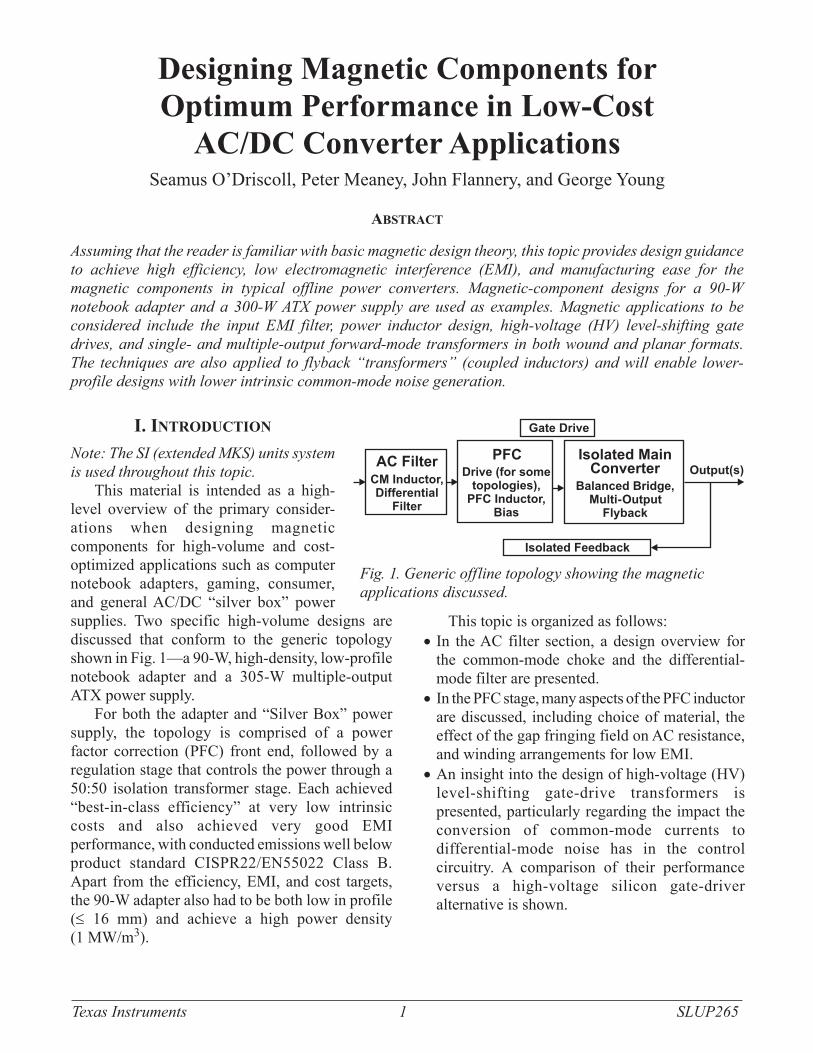
This material is intended as a high-level overview of the primary consider-ations when designing magnetic components for high-volume and cost-optimized applications such as computer notebook adapters, gaming, consumer, and general AC/DC “silver box” power supplies. Two specific high-volume designs are discussed that conform to the generic topology shown in Fig. 1—a 90-W, high-density, low-profile notebook adapter and a 305-W multiple-output ATX power supply.
For both the adapter and “Silver Box” power supply, the topology is comprised of a power factor correction (PFC) front end, followed by a regulation stage that controls the power through a 50:50 isolation transformer stage. Each achieved “best-in-class efficiency” at very low intrinsic costs and also achieved very good EMI performance, with conducted emissions well below product standard CISPR22/EN55022 Class B. Apart from the efficiency, EMI, and cost targets, the 90-W adapter also had to be both low in profile (≤ 16 mm) and achieve a high power density (1 MW/m3).
This topic is organized as follows:In the AC filter section, a design overview for •the common-mode choke and the differential-mode filter are presented.In the PFC stage, many aspects of the PFC inductor •are discussed, including choice of material, the effect of the gap fringing field on AC resistance, and winding arrangements for low EMI.An insight into the design of high-voltage (HV) •level-shifting gate-drive transformers is presented, particularly regarding the impact the conversion of common-mode currents to differential-mode noise has in the control circuitry. A comparison of their performance versus a high-voltage silicon gate-driver alternative is shown.
AC Filter
CM Inductor,
Differential
Filter
PFC
Drive (for some
topologies),
PFC Inductor,
Bias
Output(s)
Isolated Main
Converter
Balanced Bridge,
Multi-Output
Flyback
Isolated Feedback
Gate Drive
Fig. 1. Generic offline topology showing the magnetic applications discussed.
TexasInstruments 2 SLUP2655-2
Topi
c 5
The design of the power transformer for low •EMI and high efficiency is presented with a focus on balanced structure concepts. Flyback trans form ers and achieving fractional turns ratios through a “major-minor” transformer approach are also addressed.
The design techniques employed will have gen-eral applicability to the design of high-performance magnetic components across a broad range of topol ogies. Assembly drawings or photographs are presented for many of the more novel or lower-profile magnetic components.
Therefore, this topic is intended to be a holis tic and qualitative treatment of magnetic com po nent design. For a very useful treatment of basic rele vant magnetic principles, the “Magnetics Design Hand-book” from Texas Instruments [1] is recommended.
II. desIgnIng for effIcIency
The overall optimization to meet the criteria of efficiency, cost, density, and manufacturability for the topologies and magnetic components discussed in this topic has tended to maintain relatively low switching frequencies, in the range of 50 kHz to 300 kHz. Low-loss magnetic design techniques and topology choices have been exploited to simultaneously achieve surprisingly high overall density and cost performance.
A. Fundamental Magnetic Design Considerations
Magnetic design considerations are an integral part of the overall topology and switching fre-quency selection. Topology selection will depend on operating voltages and their ranges, and to a high degree on whether the topology is mostly soft-switched quasi-resonant, resonant, or hard switched. The soft-switched or resonant genres tend to allow higher switching frequencies and will place greater core- and conduction-loss challenges on the design of the magnetic component.
Higher switching frequencies will allow lower volt-seconds and operating flux-density levels per Faraday’s Law (Equation [1]). This benefit may be capitalized on as a magnetic-power processing-density increase or as a magnetic-efficiency increase.
dV N ,
dtf
= × (1)
where N is number of turns and f = magnetic flux. Equation (2) relates this flux (f) to flux density (B) via a lumped parameter Ae for an effective magnetic cross-sectional area:
eB
Af
= (2)
The design processes for both applications led to maintaining relatively low switching frequen-cies: at 100 kHz for the PFC stage and 50 kHz and 125 kHz for the bridge in the ATX supply and the adapter, respectively. This was a result of topology choices to “buck” the voltage early and therefore operate downstream stages at lower voltage. Lowering the voltage counters the increase that would otherwise occur as a result of the lower switching frequency on the operating volt-second or flux-density levels. The maintenance of lower operating flux-density levels through this general strategy of lower voltages, combined with lower frequencies, is important when one considers that core loss is a strong function of AC peak flux density. The mechanisms are through core eddy and hysteresis losses (see section 2 of Reference [1]).
Core loss for a magnetic material is generally represented by an empirical power law, usually named after Steinmetz [2, 3, 4] and given here in Equation (3):
Pv(t) k f B ,βα= × × (3)
where Pv(t) is the time-average power loss per unit volume, B is the peak flux density amplitude, f is the frequency of sinusoidal excitation, and k, α, and β are constants found by curve fitting. For the applications and frequency ranges discussed in this topic, manganese zinc (MnZn) power ferrites are used, with typical values at 100 kHz of α = 1.7 and β = 2.7 [5]. 3C96 ferrite, which was selected for optimal efficiency in these designs, has values α = 1.9 and β = 2.9 (extracted from curves in Reference [6]).
TexasInstruments 3 SLUP2655-3
Topi
c 5
DC flux density and core shape will also modify these curves, and manufacturers’ data sheets should be consulted for this impact.
Lower operating flux-density levels lead to a beneficial reduction in current ripple levels in power-path and filter components. This derives from a lumped magnetic component form (Equation [4]) of Ampere’s law giving the magnetomotive force (MMF) where H = magnetic field intensity, le denotes the effective magnetic path length, N = number of turns, and I = current:
eH l N I× = × (4)
Equation (5) gives the direct relationship between flux density, B, and field intensity, H, where µ signifies magnetic permeability:
B µH= (5)
Equation (6) gives the correspondence between current ripple and operating flux-density level. µ0 = 4π × 10-7 H/m (permeability of free space) and µr = relative permeability:
0 r ACAC
e
N IB
l
× ×µ µ ×= (6)
B. Eddy Current Loss in Windings“Skin effect” describes the tendency for AC
current in a conductor to concentrate towards the outside of the conductor and is caused by its own magnetic field. Induced eddy currents cause the penetrating field and consequent net current density to decay to 1/e times the surface current density at the skin depth.
“Proximity loss” also causes concentration of current densities, usually to either side of a winding layer, but it is caused by the overall field through the winding space. There are many references to these effects, such as in [1] or [4].
Proximity loss is easiest to consider for the case of a single winding or an ungapped inductor. First consider a single turn with a “going” and “return” current. Current will crowd towards the center of the magnetic structure, between the “going” and “return” current turns (consistent with the natural tendency to achieve lowest inductance and stored energy). For multiple layers in either of the “going” or “return” layers, this effect will
combine with a transformer action (primary with equal and opposite induced secondary) at each layer-to-layer interface to cause a successive increase in proximity loss effect as one traverses from layer to layer. Alternatively, consider an increasing winding space field due to the increasing MMF as the layers are traversed. Here the overall field for the winding is considered to be predominantly tangential to each winding layer. The loss equations for a multiple layer winding were originally presented in Reference [13]. For an inductor, the proximity loss will depend on the main AC inductor current. A reduction in inductor current ripple will help reduce this loss.
For a gapped inductor or coupled inductor (flyback “transformer”), the gap field will produce a component of winding space field which will be normal to the main proximity-effect field. This is referred to here as gap-fringe proximity. It can often be the most significant copper loss mechanism, particularly for foil-type windings where the copper paths for substantial eddy-current flows will be present. Gap fringe proximity also generates localized hot-spots.
For a transformer scenario, the primary power-current MMF will be substan tially cancelled by the transformed equal and opposite secondary power current in each half of the winding space. The winding-space MMF will therefore be comprised of a magnetizing field and a leakage field, and hence the proximity effect in a transformer winding space is often associated with the leakage inductance. The proximity effect will indeed vary with frequency and is associated with a reduction in leakage inductance with increasing frequency. Reference [14] provides graphical explanations as to how proximity loss in each half-winding space of a transformer is comparable to that of a single winding inductor.
Transition loss categorizes eddy loss during an interval when current is commutated from one winding to another. Transition loss in the flyback occurs during the relatively short commutation interval, during which time, neither the overall winding-space field nor the gap fringe field change very much. However, during this time, there is local field movement from primary to secondary and vice versa. The copper losses in an example

TexasInstruments 4 SLUP2655-4
Topi
c 5
flyback converter are analyzed in Reference [7] and the results are presented to show that transition copper losses may be ten times as significant as other eddy-loss mechanisms.
Overall AC resistance may be evaluated by considering each individual harmonic and applying Dowell-type analysis or Finite-Element analysis. Alternatively, as derived in Reference [9], for any arbitrary current waveform, the effective resistance (Reff) subject to certain restrictions on layer thickness is related to the rms current (Irms) via Equation (7).
2
eff
I rmsR 1 k Irms
∝ + ω×
′
(7)
Here k is a constant that is dependent on both the number of winding layers and the layer-thickness to skin-depth ratio, with skin depth taken at the fundamental frequency. Also, I′rms denotes the first derivative and w is the fundamental angular frequency. The relationship in Equation (7) gives an insight into why transition loss may be so significant. For example, transition-loss mitigation techniques that use leakage-clamp circuits may become important tools for slowing commutation di/dt and thereby minimizing the effects of commutation leakage. The accuracy of Equation (7) is subject to certain restrictions on layer thickness.
A lower switching frequency leads to a lower fundamental and lower frequency harmonics in current waveforms. This then minimizes the AC winding loss through skin effect, proximity loss, and transition loss.
Particularly for flyback converters, selecting a turns ratio biased towards lowering the normal steady-state operating duty cycle and consequent flux ripple tends to pay more dividends in efficiency than erring on the side of higher stored energies. Experience has shown that transition loss is a surprisingly high component of total copper loss in a flyback transformer. Reducing the magnitude of AC flux or current ripple will reduce this major practical component of loss.
C. Magnetic Manufacturing Strategy Considerations
The manufacturing strategy for the magnetic components is an integral part of overall topology selection and operating voltage levels for each stage. It will also have a strong influence on the balance of magnetic cross-section (Ae) versus turns count.
The isolation stage transformer choice has tended to be planar or hybrid wound-planar, employing copper foils for the low voltage side. A low-profile or low-area footprint, a high copper-fill ratio, and achieving low-loss interconnect with associated power semiconductors have been the motivators. This strategy, combined with “bucked” down volt-ages, has led to a single-turn secondary as being a good choice for low-voltage outputs in terms of copper loss, cost, and practicality. Safety isolation has been achieved by the use of triple-insulated insulation systems. Parallel half turns have further conduction loss merit, but they require much more careful design to achieve AC and DC balance.
Getting to the lowest number of actual turns on either the primary or secondary is not an absolute strategy, however. For high voltages or lower currents—and particularly for conventional wound magnetic components—a higher turns count, lower Ae, and using lighter wires with smaller diameters may be the correct strategy. For a lower turns count and higher currents, wound components become tedious with regards to managing parallel strands and interconnect. This has led to the adop-tion of copper foils. The practical design techniques for wound transformers are not a focus in this topic. They have different practical considerations regarding copper fill factor and safety isolation. Proximity loss influence as per Dowell will be very important for this construction and is well covered in Reference [4]. Wire or track ingress/ egress is always an area that can be optimized. Minimizing crossovers in wound components and vias in planar circuits is also important.
Note also that the achievable copper fill factor may be influenced by the combination of the desired manufacturing technology, the safety system, and the topology choices—including turns ratio.
TexasInstruments 5 SLUP2655-5
Topi
c 5
D. Balanced StructuresAnother general theme for high efficiency and
low EMI is the employment of balanced transformer structures and operating modes. The containment of EMI at each source leads to lower unit-level emissions, with consequently lower overall costs. The term “balanced” here has a number of parallel interpretations.
Core FluxAn operating mode should be chosen to have
an inherent energy reset to actively return operating flux levels to zero (balanced) and at controlled rates of change by the end of every power transfer cycle [8]. One such mode is integral cycle control (ICC), in which power is delivered to the output in finite packets with zero net-magnetizing current. This will occur over all load ranges, including transients and is particularly important for burst-mode type systems. The idea is to minimise higher magnitude and higher frequency reset of magnetic field energy. Symmetrical flux excursions about zero will also minimize the peak flux density level. Bridge, active-clamp or resonant-type topologies naturally achieve this. Unclamped flyback-type systems will tend have higher frequency and higher magnitude flux excursions leading to an increase in EMI from a number of mechanisms; including magnetic near-field (inductive coupling) and electric near-field (capacitive coupling).
Electrostatic ConsiderationsMagnetic components should appear from the
outside as being electrostatically at a low or DC potential. This applies to both windings and core. Balanced operation will mean that windings are arranged where possible to swing spatially such that internal capacitive (displacement) current common-mode generators are minimized and combine to return all such generated currents locally and internal to the structure. These currents will cause winding loss, but more importantly, if not returned internally, they will generate EMI-causing surface electrostatic fields; or winding and core voltages will be created to return the currents through external common-mode current paths. Also structures such as the conventional
full bridge can have a “virtual” ground position in the middle of the winding. Winding voltages will be balanced about this point and this will lead to the lowest magnitude situation for capacitive current or common-mode current generators.
High-Voltage Isolation Transformer CM-to-DM Balance
Balanced will also mean, for example, in the case of HV gate-driver transformers, that common-mode (CM) currents that do flow will cause no net adverse conversions to differential mode (DM). This means that CM currents from the primary to the secondary of such a transformer can be arranged to flow in a balanced, equal, and opposite winding configuration for mutual self cancellation of such adverse DM disturbances.
MMF ProfileConsidering efficiency, transformer structures
with interleaved windings will tend to have the lowest overall loss because the leakage field or MMF-profile magnitude is minimized. Symmet-rical MMF profiles consistent with balanced windings or MMF generation will also tend to have the lowest loss. Section R2 of Reference [1] shows how winding-space MMF or leakage field, combined with the magnetizing field, causes proximity loss. The goal is to minimize the amount of copper which is exposed to a large proximity field (MMF). This applies to unused portions of windings such as the non-energized half of a center tap or a screen. For the case of multiple secondaries with varying MMFs, it may be appropriate to arrange windings such that the highest MMF windings are closest to the primary so that MMF is quickly cancelled over the least amount of winding space.
E. Low EMIA final overall theme is to intrinsically or
struc turally design for low EMI. Magnetic com po-nents are designed to appear externally as being at low magnetic potential. Air gaps and “hot” ends of windings are confined to the center of components where possible. Judicious positioning and orien ta-tion may be exploited to eliminate the requirements for dissipative flux bands or magnetic screens.

TexasInstruments 6 SLUP2655-6
Topi
c 5
III. common-mode choke And dIfferentIAl Input fIlter
The schematic in Fig. 2 shows the main com-po nents in the input filter (common-mode choke, differential-mode inductor) for an offline power supply and buck PFC stage.
A. Common-Mode ChokeThe common-mode (CM) core has high
permeability: µi = 10,000 (initial permeability pertains to small-amplitude AC field strength relative to free space µ0), and is appropriate for the CM inductor because of the very-low core flux densities involved. The windings are such that there is no substantial net differential-mode (DM) voltage. In the high-density design shown in Fig. 3, it is not possible to take advantage of split windings. The windings are wound bifilar such
that any stray linked magnetic field will induce equal and opposite voltages in each winding, thus preventing the conversion to DM noise voltages per Equation (1). The spacing between each turn is controlled to minimize self capacitance and create a higher impedance to higher frequency. In this case, voltage isolation is achieved through the use of insulated wire, as shown in the photograph in Fig. 3. The orientation of the toroid axis is chosen to minimize stray magnetic field coupling, which can be one of the difficulties with CM filter chokes. Equation (1), Equation (5), and Equation (6) (adapted for stray field) show that the high perme-ability of the core could transform a significant CM noise voltage to the input stage of the power supply to create EMI problems. The main source of any stray magnetic field in this case is the gap in the adjacent PFC choke. The first step in
Fig. 2. Schematic showing input filter and buck PFC stage (PFC stage can be high- or low-side drive).
Intermediate
DC Bus
Differential-
Mode Filter
Common-
Mode
Inductor
AC
Bridge
Rectifier
Gate
Drive
PFC
Inductor
PFC FET
Bulk Cap
Y Cap
Fig. 3. Main magnetic components as implemented in the 90-W notebook adapter.
Differential-Input
Filter (2 Stage)
Output Inductor
PFC Inductor
Isolation
Transformer
CM Inductor

TexasInstruments 7 SLUP2655-7
Topi
c 5
resolving the CM EMI issue is to adjust the core size, loca tion, and orientation relative to other gapped mag netic components.
A magnetic material such as steel could be used to perform magnetic shielding and would theoretically reduce stray magnetic field coupling. Practically, however, wrapping the toroid in copper foil is effective in reducing EMI. Copper foil provides effective E-field shielding, an energy-dissipating action for stray fields, and some short-circuit action for noise toward the higher-frequency end of the conducted EMI range (10 to 30 MHz), which will be capacitively coupled to the foil screen.
For this particular design, very good EMI attenuation was achieved by bifilar winding, orientation, and location. There was no need to resort to a copper-foil wrap for the EMI choke. Nevertheless, the solution was discussed because the EMI challenge increases commensurate with density increase.
B. Differential-Mode InductorA Pi or T differential filter format is typically
chosen for the higher attenuation it will provide for a given filter size. This will generally give better attenuation at the switching frequency and its higher harmonics, but one must be careful to
not create cascade LC resonant effects at some higher frequencies. Because of the physical space constraints associated with these designs, this inductor was split into two individual serially connected components.
IV. pfc choke Inductor
For this section, it is assumed that the desired value of inductance, L, is known. For a gapped inductor design, it is difficult to be very prescriptive about the design process; but the theory presented in this section should allow iteration to an efficient low-cost design.
Fig. 4 shows typical 100-kHz core-loss density plots for good powdered iron, distributed-gap material versus a good power ferrite material. The lower loss of ferrite, coupled with the ease of manufacturability—particularly when additional separate bias or sense windings are required—has led to the selection of EE-type ferrite core shapes.
The data upon which the plots in Fig. 4 are based was obtained by measuring toroid cores. To calculate core loss in other core shapes, manu-facturers often quote loss data for a given material for various individual core shapes. For many common ferrite core-set shapes, actual core loss could be as much as two times greater than that for the toroid in the same material.
1x10
1x10
1000
100
10
1
0.1
0.01
5
4
0.01 0.1 1
Peak Flux (T)
Co
re L
oss
(
kW
/m
)
3
PV
Ferrite
PV
Powdered_Iron
Fig. 4. Core loss comparison at 100 kHz for powdered iron versus power ferrite.
TexasInstruments 8 SLUP2655-8
Topi
c 5
The basic equations used to calculate AC and DC flux density are shown. Methods to reduce the AC copper loss caused by the gap fringe field and EMI considerations are presented.
A. Basic Equations for Inductor DesignBasic calculations will ensure that:
1. The required nominal inductance, L, is achieved.
2. The total flux density, BTOT, never exceeds a maximum saturation value, BSAT.
3. The total core and copper loss remain within temperature limits or efficiency criteria.
Inductance is calculated based on the lumped reluctance (R) of the magnetic circuit, i.e. the core and the gap. The reluctance of a magnetic circuit is given as:
e
e
l,
A=µ
R (8)
where le is the magnetic path length and Ae is the cross-sectional area of the magnetic material. The circuit reluctance, R, along with Equation (2), Equation (4), and Equation (5), may be combined to create a lumped magnetic circuit equation analogous to Ohm’s law, where MMF is the magnetomotive force and f is the magnetic flux:
MMF = f×R (9)The reluctance of the core and the gap (assuming a core with a square center leg) are calculated using Equation (10) and Equation (11):
e
core0 r e
l
A=µ µ× ×
R (10)
ggap 2
0 e g
l
( A l ) ×=µ +
R
(11)
Equation (11) contains a factor to represent the fact that the flux fringe at the gap creates an effective cross-sectional area increase in the gap region. There are many approximations for this, depending on the overall structural geometry and the relative gap size. But this formula gives an inductance calculation that correlates well for the
inductor designs here. This is a representation of the material, by Lloyd Dixon, in Section 5 of Reference [1]. L/N2 is often denoted as AL and is the recip rocal of reluctance, R:
L
core gap
1A
=+R R
(12)
The total flux (combination of DC and peak AC contribution) in the core must be less than the saturation flux density of the material:
DC AC TOT SAT
ˆ ˆB B B B+ = ≤ (13)
The DC current will establish a DC flux density, BDC, which may be calculated based on the peak DC current handling required:
DCDC
gap core e
I NB
( ) A =
+ ××
R R (14)
The ferrite gap needs to be adjusted to support the worst-case peak-current requirement of the inductor. The gap extension increases the gap reluctance, Rgap, to reduce the flux density, BDC. For a gapped structure (assuming that the bulk of the energy resides in the gap), Equation (15) (an approximation to Equation [14]) serves as a rough check for flux density:
0 DCDC
g
N IB
lµ × ×
= (15)
L
ACe
V DB
2 N A f××
=× ×
(16)
BAC is the peak amplitude of the AC flux density. VL and D may be calculated for either the positive or negative volt-seconds applied to the inductor. The factor of 2 in Equation (16) assumes sym met-rical AC flux swings about a DC midpoint. It will be valid for transformer situations and inductors that operate with relatively small discontinuous regions. The iterative process of identifying a suit-able core, number of turns, and required gap length is well documented in section 5 of Reference [1]. Flux-density calculations must be valid for all transient situations, such as during start-up or short circuit, where there may not be sufficient volt-seconds for reset.
TexasInstruments 9 SLUP2655-9
Topi
c 5
B. Copper Loss Due to the Gap Fringe Field
An accurate prediction of copper loss in a gapped inductor is tricky to achieve, requiring a finite-element analysis at a collection of the signif icant waveform harmonics [9] while replicating the exact winding configuration. The reduction of inductor copper loss is, however, relatively easy to achieve using the techniques described in the fol low ing sections. These include performing analysis using only the significant harmonics and simpli fying models with approximations to the actual wind ing configurations.
The gap creates an AC fringe field, which is most likely the most significant contribution to AC copper loss. The loss profile for a 22-turn, 55-µH, 100-kHz inductor based on a PQ26/25 core set with a 1.8-mm gap length for a 305-W PFC inductor is used here to illustrate the scale of fringe-field effect on copper loss and the steps that can be taken to reduce this.
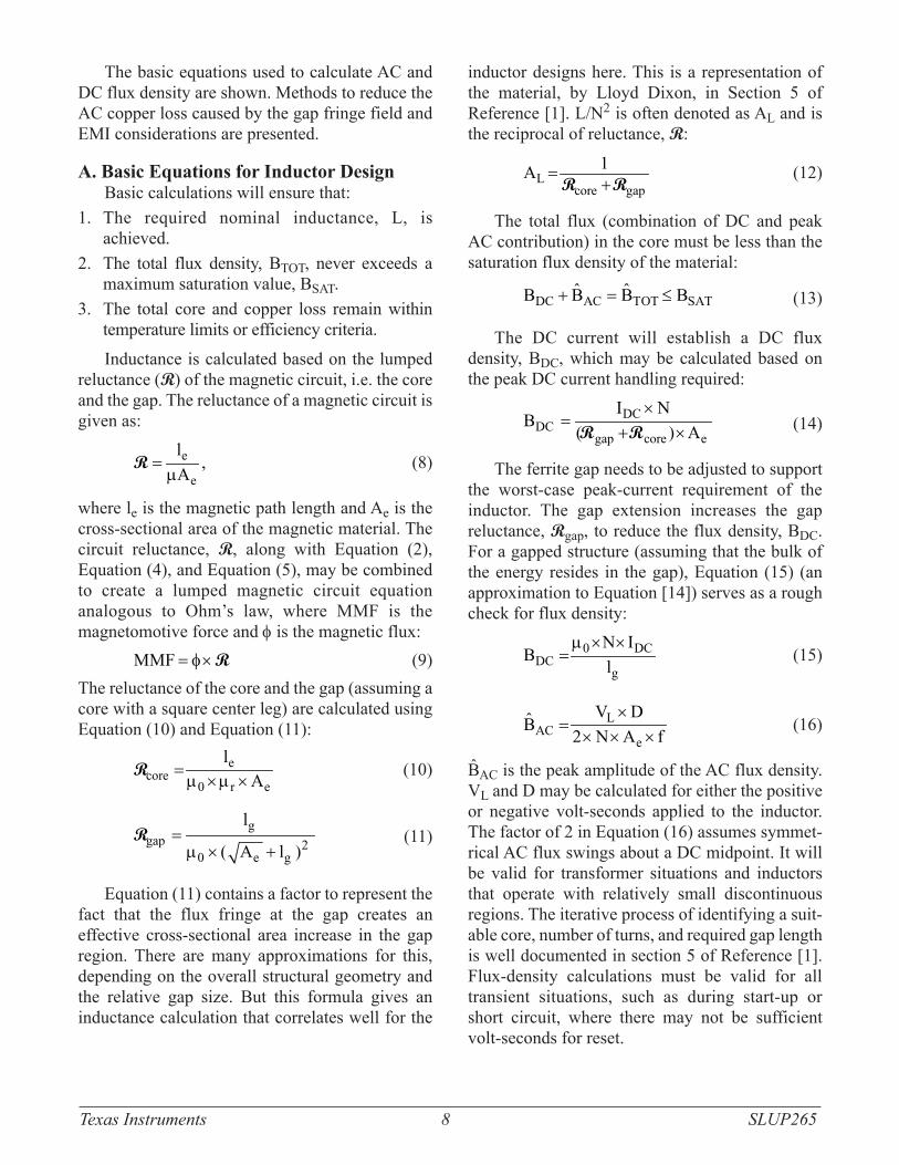
Captured with ANSYS, Inc., Maxwell® field-simulation software, Fig. 5 shows some of the results of a finite-element model of the 22-turn inductor, wound with 1.1-mm enameled copper wire (ECW) with 1 A per turn. The plots showing loss distri bution in the copper turns at 100 kHz clearly show the extremely high loss associated with the gap fringe field. Fig. 5a shows the full core cross-section; Figs. 5b and 5c show just the window area of this 2D, axi-symmetric model.
The combination of skin effect, proximity effect, and gap-fringe proximity effect con trib-ute to an FR >> 1. FR is the ratio of AC resist-ance to DC resistance for a given frequency:
ACR
DC
RF
R=
(17)
Fig. 5c shows what would happen if the gapped ferrite material were replaced with an equivalent inductance-distributed gap material such as powdered iron. FR for this case is seen to reduce fourfold. This indicates that 75% of the AC loss for this structure derives from the proximity loss caused by the fringe field.
Fig. 5. Results of finite-element model.
Core Loss
(
kW/m
)
3
1000.0
533.67
284.80
151.99
81.11
43.29
23.10
12.33
6.58
3.51
1.87
1.00
a. Cross-section through PQ26/25 core set with 3C96 ferrite, a center gap of 1.8 mm, 22 turns of 1.1-mm ECW at 105°C, and RDC = 0.0302 Ω.
b. Copper loss at 100 kHz with RAC = 0.964 Ω and FR = 32.
c. Copper loss with a distributed gap core (µ) of 40 (for equivalent inductance), RAC = 0.249 Ω, and FR = 8.2.
TexasInstruments 10 SLUP2655-10
Topi
c 5
Although the use of a distributed gap core such as a toroid might seem attractive from an AC copper-loss point of view, these materials typically display a much higher core loss than power ferrite materials (Fig. 4). So in every design, an engineering trade-off must be made between core loss, copper loss, size, and cost. For both reference designs, a gapped ferrite core yielded the required optimum perfor-mance from a size, overall loss, and manu factur-ability perspective. Copper-loss issues are dealt with in the following sections.
Skin effect [1, 4] can be dealt with by using wire strands of diameter less that the skin depth, bearing in mind the influence of higher-order harmonics. Skin depth (δ) is calculated using Equation (18), where ρ is the resistivity of copper at the required temperature and f is the frequency:
0
fρ
δ = π× ×µ (18)
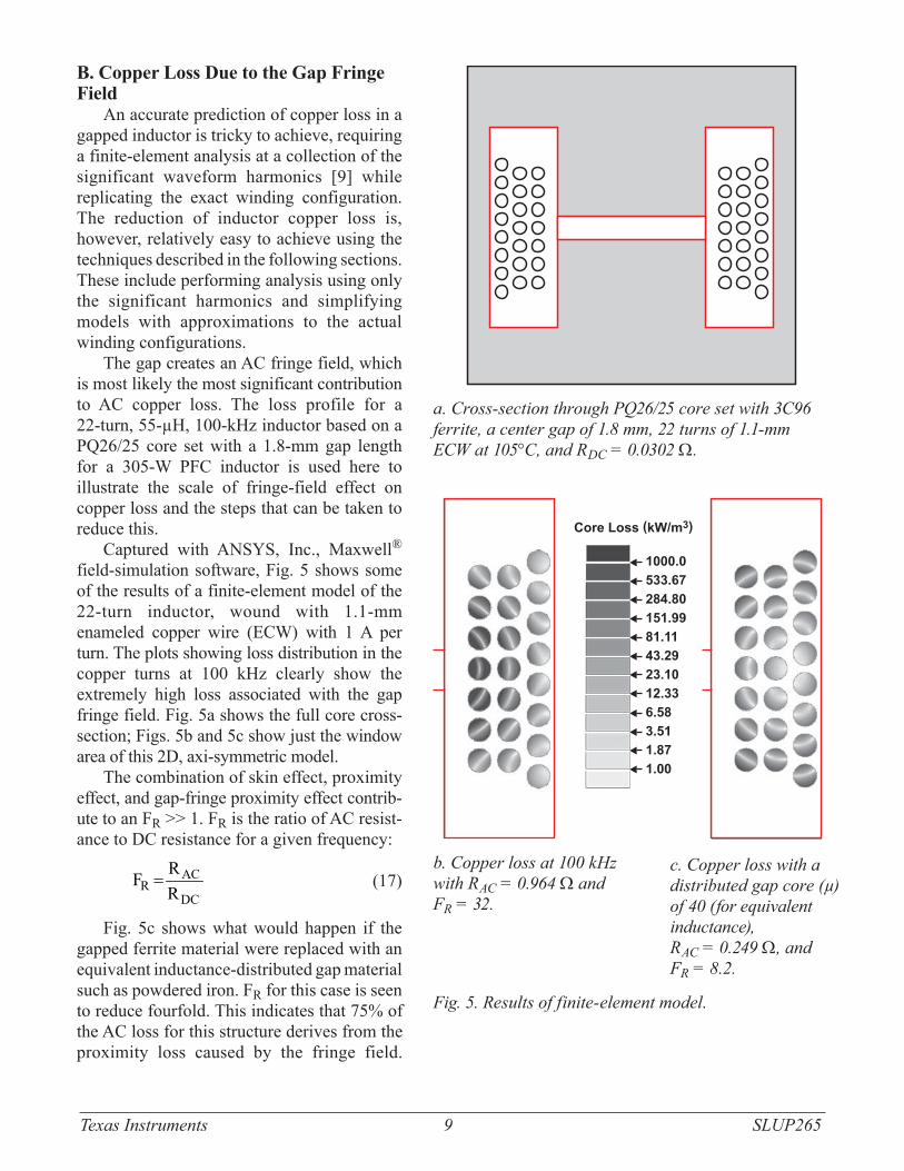
Equation (18) gives the skin depth for copper at 105°C and 100 kHz as 0.24 mm. For this design, multi-stranded wires of 0.1 mm diameter were chosen. Empirically, it was found that a twisted bundle of 126 strands of 0.1-mm ECW gave lowest overall loss. Fig. 6 shows a similar finite-element model of one of the design iterations (91 × 0.1-mm strands), which shows the FR reduction achievable (FR = 1.8) through a reduction of strand diameter to 0.1 mm.
The 2D finite-element model does not account for the increased benefit of using Litz wire, or a “poor man’s Litz” formed by twisting a bundle of normal ECW strands. Twisting is not quite as good as Litz, which has each turn passing through the center point to guarantee equal net currents in each of the strands. The degree of twisting performed does have a dramatic effect on the resulting copper losses. There should be considerably more than two complete twists per mean length per turn (MLT). Power-supply efficiency differences of up to 0.7% were observed, depending on the degree of twisting of the strands in the bundle. This supports the fact that fringe-field proximity is the primary consideration. Four to six twists per MLT is not overkill; the greater reduction in RAC more than compensates for the increased RDC, due to the lengthening of each strand. This required
number of twists is necessary to get a reasonable degree of twisting on the inner strands of the bundle. An FR of 1.8 is shown in Fig. 6 for 90 × 0.1-mm parallel strands.
Experiments with turns of “blocking tape” positioned in the center of the bobbin were also carried out. The purpose was to physically prevent the windings from encroaching on the more intense portion of the gap field, but it is unclear if there is an overall efficiency benefit. The trade-off is in the reduction in useable window area. However, it is recommended to assess the worst-case winding temperature close to the air gap during power-supply qualification. This can usually be achieved by introducing a thermocouple into the bobbin/winding structure.
Fig. 6 shows a loss simulation with the window area of a PQ26/25 core set with 3C96 ferrite, a gap of 1.8 mm, and 22 turns of 91 × 0.1-mm ECW at 105°C. Each strand in each bundle is forced to carry equal current to model perfect current share. For this simulation, RDC = 0.039 Ω, RAC = 0.071 Ω, and FR = 1.8.
C. EMI Considerations for the PFC InductorThere are a few basic techniques to bear in
mind that should give a good reduction in EMI. The winding direction is important from both an efficiency and EMI perspective.
The circuit in Fig. 7 shows the “cold” and “hot” ends of the inductor winding from an EMI electro-static perspective. Hot refers to having rela tively
Core Loss
(
kW/m
)
3
100.0
90.1
80.2
70.3
60.4
50.5
40.6
30.7
20.8
10.9
1.0
Fig. 6. 2D model showing copper loss in PFC inductor at 100 kHz with 0.1-mm copper strands.

TexasInstruments 11 SLUP2655-11
Topi
c 5
large (magnitude and frequency) AC voltage. The windings will self-shield, electro stat ically, if the hot end is positioned closest to the center leg of the core and the windings are wound toward the quiet or cold finish on the outside. This technique may obviate the need for an outer grounded electrostatic shield.
Lower fringe-field induced loss in the windings can occur for evenly distributed gaps in center and outer legs, but managing outer-leg gaps presents a significant mechanical challenge and would neces-sitate magnetic-field leakage containment. Should the design constraints for the particular appli ca tion (size, cost, core versus copper loss) require a gapped ferrite core, the approach recom mended here is to have the higher fringe field concentrated in the center of the struc ture and employ multi-strands of small diam eter wire to mitigate the extra copper loss.
V. hIgh-VoltAge, leVel-shIftIng, gAte-drIVer
trAnsformer
A high-side or galvanically isolated power MOSFET drive is a requirement fre-quently encountered in power electronics. A high-side drive at varying voltages up to 500 V is common for high-side bridge MOSFETs supplied from a boost PFC pre-regulator stage. Some “bridgeless” topol-ogies will require a high-side drive at line voltages. A buck PFC may or may not
require a high-side drive, depending on the topology selected. Gate-drive circuits themselves may be of a wide variety of topologies: forward mode such as push-pull and bridge are frequently used. A resonant reset or active clamp-type circuit will also give very low loss and was the design choice here. Note that the resonant reset frequency may limit the range of duty cycles achievable. A schematic of a transformer-based, resonant-reset, gate-drive circuit for a high-side drive is shown in Fig. 8. In this circuit, the resonant components are the magnetizing inductance of the transformer, the drain-source capacitance (CDS) of the FET, and all of the secondary-side capac itance reflected through the transformer.
Fig. 7. High-side driven PFC inductor showing “hot” and “cold” ends for both buck and boost.
Switch
Node
High Voltage
Main High-
Side FET
C
in
C
ds
L
pfc
C
bulk
ColdHot
a. Buck PFC
Switch
Node
C
in
C
DS
L
pfc
C
bulk
Cold Hot
b. Boost PFC
Fig. 8. Level-shifting transformer circuit (resonant reset example). L could be either a buck inductor or the primary of a bridge-output transformer.
Transformer
HighVoltage
Q-GateDriver
PowerMOSFET
Low-SideSwitch
SwitchNode
Vbias
Wpa Wsa
L
–Vpri
Gate-DriveIC
PWMin GD

TexasInstruments 12 SLUP2655-12
Topi
c 5
The capacitive currents and the conversion to DM disturbances, the focus of this section, are appli cable irrespective of gate-drive topology and deployment.
For a high-side drive, there are two commonly used choices: either high-voltage or isolated silicon-driver ICs in combination with bootstrapped power supplies, or gate-drive transformers with some dis-crete diode/transistor drive and rectifier circuits. Both approaches have merit. This section explains how to balance windings and how balanced windings overcome the biggest difficulty with high-voltage gate-driver transformers: common-mode noise generation in the control circuitry. At the end of this section, a comparison of gate-driver transformer circuits and silicon-driver ICs is presented.
To get acceptable gate-driver transformer per-formance, the leakage inductance between primary and secondary must be minimized, usually with a bifilar winding arrangement. The difficulty arises because obtaining a reduced leakage inductance will cause increased capacitance between primary and secondary, CP-S. See Appendix A for a treat-ment on this capacitance. Because the switch-node voltage of the power circuit (Fig. 7) is so large relative to the driver voltage, CP-S is effectively equal to the physical capacitance, which is mea-sured between the windings. Consider also that the switch node may slew at rates of up to 50 V/ns. This high dV/dt might occur during high current pulses in a bridge or with very high-gm super-junction power MOSFETs, to give two examples. This causes the common-mode current, ICM, to flow between pri mary and secondary of the gate-driver transformer. It might be mitigated by the insertion of a capacitive screen between primary and secondary, but the screen would increase leakage inductance or be completely impractical for a magnetic core such as a toroid. This current may cause serious noise interference in the control circuitry.
For a typical gate-driver transformer in a 220-VAC offline application, peak common-mode cur rent in the 1-A to 2-A range was measured.
The circuit in Fig. 9 was used to measure ICM through the primary winding(s) for the gate-driver transformers under test. A high-mu toroid, EPCOS B64290L0697X038, was used. The transformer
feed and return make a single pass through the center of the core. A 22-turn secondary, ballasted by a 22-Ω shunt, gives 1 V/A.
The toroidal gate-driver transformers that were wound exhibited self-resonant frequencies around 400 kHz. This parameter should be well above the switching frequency to minimize gate-drive circuit- supply current and waveform-distortion effects.
A. Degradation of Gate Drive Due to Conversion of Common Mode to Differential Mode
A more serious difficulty with common-mode (CM) current is that it causes a differential-mode (DM) voltage effect at both the primary and secondary, which acts to counteract desired drive behavior. Depend ing on circuit parameters, this CM to DM feedback has a threshold, up to which there may be no discernible impact of this capacitive current on switching waveforms—and beyond which a gross slowing of MOSFET switching will occur. The key parameters include transformed drive cur rent, reverse common-mode current, MOSFET gm, MOSFET CGS, and MOSFET CGS:CDS ratio. Higher-CP-S transformers and lower-power (higher-RDSON) MOSFETs will exhibit greater sensitivity to this adverse DM effect on switching behavior.
B. Solution for Differential-Mode Degradation Effect
This differential-mode degradation effect may be very successfully prevented by adding two extra single-ended balancing windings (Wpb and Wsb), shown in Fig. 10. Optimum results and practicality
W
pa
I
CM
Fig. 9. Circuit for measurement of common-mode current in the gate-drive circuit.
TexasInstruments 13 SLUP2655-13
Topi
c 5
will deem that Wpa, Wpb, Wsa, and Wsb should be wound quadfilar. One end of each of Wpb and Wsb are electrically connected to their respec tive active winding, with the “free” ends insulated and secured mechanically.
These quadfilar windings were found to be highly effective. ICM in either Wsa or Wpa can be thought of as transforming opposite capac i-tive currents in Wsb and Wpb to cancel the DM disturbance in either side, respectively.
The quadfilar arrangement is very effective in that it reduces the DM disturbance in both the driving side and the driven side of the gate-drive circuit. A trifilar arrangement consisting of Wpa, Wsa, and a single cancellation winding, Wsb—which is connected to the switch node at the power MOSFET—also shows very good benefit.
Additionally, this technique allows for close coupling of all windings and is consistent with achieving the lowest leakage inductance possible. This will reduce driver propagation delay and energy loss due to leakage energy reset.
Note that the balancing windings do not reduce ICM. In fact, they typically double CP-S but cause nearly all of the ICM to be harmlessly returned through the decoupled supply rails.
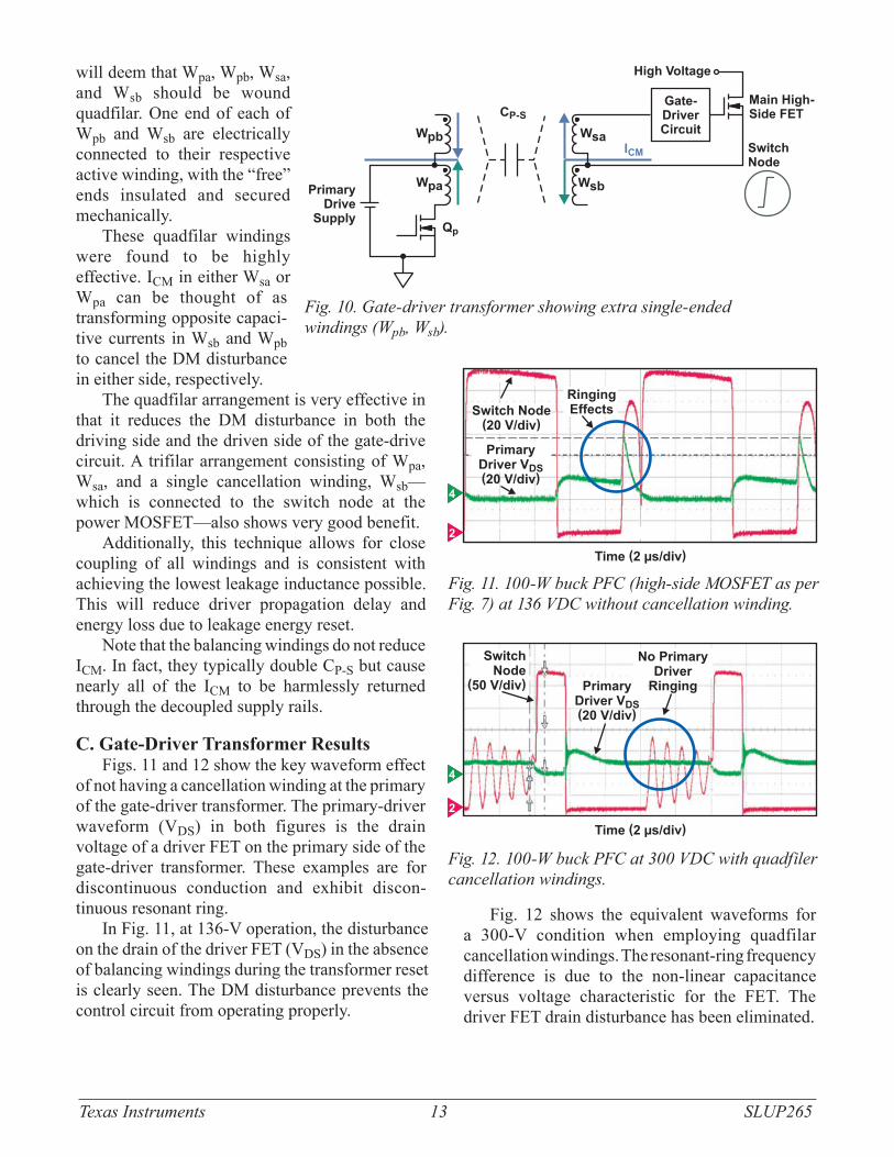
C. Gate-Driver Transformer ResultsFigs. 11 and 12 show the key waveform effect
of not having a cancellation winding at the primary of the gate-driver transformer. The primary-driver waveform (VDS) in both figures is the drain voltage of a driver FET on the primary side of the gate-driver transformer. These examples are for discontinuous conduction and exhibit dis con-tinuous resonant ring.
In Fig. 11, at 136-V operation, the disturbance on the drain of the driver FET (VDS) in the absence of balancing windings during the transformer reset is clearly seen. The DM disturbance prevents the control circuit from operating properly.
C
P-S
Main High-
Side FET
High Voltage
Gate-
Driver
Circuit
Switch
Node
W
pa
Q
p
W
pb
Primary
Drive
Supply
W
sa
I
CM
W
sb
Fig. 10. Gate-driver transformer showing extra single-ended windings (Wpb, Wsb).
Fig. 12 shows the equivalent waveforms for a 300-V condition when employing quadfilar cancellation windings. The resonant-ring frequency difference is due to the non-linear capacitance versus voltage characteristic for the FET. The driver FET drain disturbance has been eliminated.
Time
(
2 µs/div
)
2
4
Switch Node
(
20 V/div
)
Ringing
Effects
Primary
Driver V
(
20 V/div
)
DS
Fig. 11. 100-W buck PFC (high-side MOSFET as per Fig. 7) at 136 VDC without cancellation winding.
Time
(
2 µs/div
)
2
4
Switch
Node
(
50 V/div
)
Primary
Driver V
(
20 V/div
)
DS
No Primary
Driver
Ringing
Fig. 12. 100-W buck PFC at 300 VDC with quadfiler cancellation windings.

TexasInstruments 14 SLUP2655-14
Topi
c 5
Note that the disturbance on the drain of the gate-driver FET is not the main issue but it does give an indication of the CM injection. The real issue is the potential for slowing the switching speed of the power MOSFET. Fig. 13 shows the effects on the gate drive when the sensitivity to the CM to DM effect was increased by chang ing the power MOSFET from a 199-mΩ device to a 385-mΩ device. The CP-S of the gate-driver transformer was also increased by increas ing the number of primary and secondary turns (Np and Ns) in ratio. The turn-off time (Miller region traverse, which is the flat section of VGS) extended from 20 ns to 600 ns by not having DM cancellation windings. Note that the beneficial effect of the balancing windings on the switching behavior for the 199-mΩ MOSFET was not discernible. However, with increased gate-driver trans-former capacitance and a 385-mΩ MOSFET (lower capacitance, smaller die), the effect is dramatic. This is why margin testing against this effect must be conducted.
D. Driver Transformer Comparison with HV Gate-Driver ICs
For power-supply applications where the gate drive is required to cross the safety isolation barrier, a transformer-based solution may be the only choice. For other applications, a silicon-based solution may be an option.
Gate-driver ICs (500-V to 700-V rating) typi cally have their drivers in high-voltage, reverse-junction-isolated silicon wells. These isolated well capacitances give an effective common-mode capacitance that is typically less than a few picofarads. Gate-driver transformers will typically have 20 pF to 50 pF of interwinding capacitance. The power circuit under consideration, when tested with a high-voltage driver IC, gave an ICM_PEAK of 20 mA, a hugely beneficial, fifty-fold reduction over the gate-driver transformer.
For any transformer there will be a volt-second balance question. Requiring a transformer to achieve an 80% duty cycle for a 10-V drive will require an average of 40 V for reset. In reality, reset schemes will require higher voltages; hence, quite high voltage
3
2
Time
(
40 ns/div
)
1
V
(
5 V/div
)
GS
20-ns
Miller Region
a. Quadfilar cancellation.
3
2
Time
(
400 ns/div
)
1
V
(
5 V/div
)
GS
600-ns
Miller Region
b. No cancellation windings.
Fig. 13. Example of turn-off condition for VGS of high-side FET.

TexasInstruments 15 SLUP2655-15
Topi
c 5
ratings will be required in driver components on each side of the transformer. Resonant reset, for instance, might require 200-V components for 80% duty, depending on the tolerance obtainable on the reset ring frequency.
Operating transformers at a greater than 80% duty cycle will practically require dual transformers
configured so that each may support 50% of the volt-seconds, or more complicated push-pull arrangements with separate circuitry to manage turn on and turn off.
Table 1 provides a summary of issues to consider when evaluating transformer- and silicon-driver options.
tAble 1. compArIson of mAgnetIc Versus sIlIcon drIVers
Transformer Gate Drives HV Silicon-Driver ICsHigh voltage or safety isolation may be achieved easily by using an approved insulation system comprising blocking tape or insulated wire.
Safety isolation will require more specialized and costly ICs.
1-mA to 2-mA typical magnetizing quiescent supply current for non-resonant circuits. Resonant or active-clamp-type drive schemes are a small percentage of this, probably < 200 µA.
Quiescent supply current typically 100 µA to 300 µA.
Low-impedance, discrete silicon driver will be required on the primary and secondary sides of the transformer.
Better use of driver silicon and compatibility, with a high degree of silicon or packaging integration.
Practical limit of 70% to 80% duty cycles because of transformer volt-second reset requirement.
No intrinsic duty-cycle limit. It may be advantageous to have a fully-on drive for many cycles. Subject to bootstrap capaci-tor charge and discharge management.
CP-S may typically range from 10 pF to 100 pF. Expensive shielding between primary and secondary windings may be required to get low CM noise-current injection into control circuitry. Unfortunately, such shielding is often not practical.
CP-S may typically be a few pF for 700-V silicon. Extremely low CM noise-current injection into control circuitry.
CM conversion to DM drive self-disturbance may require balancing windings.
Much lower CM disturbance currents and circuitry tech-niques to counteract DM disturbance will be integrated in the driver IC.
Close coupling of windings and low leakage structures can ideally get zero propagation delay in the magnetic. But prac tically, reduction of CP-S (to reduce CM noise injection) means that the leakage inductance will be increased to a level to give comparable propagation delay to the silicon solution. Also, the double requirement for additional discrete low-impedance drivers and rectifiers adds to propagation delays.
Fast level shifting to high-side drive and propagation delays of typically 20 ns to 70 ns.
If a push-pull drive is used on the primary, all gate-drive power can be transferred as part of the gate-drive signal, thus obviating the need for a bootstrap bias supply.
A separate DC bias circuitry will be required.

TexasInstruments 16 SLUP2655-16
Topi
c 5
VI. trAnsformer desIgn for low emI
The 90-W adapter transformer (125-kHz half-bridge operating from 80 VDC) shown in Fig 3 is used here to illustrate the concept of maintaining CM generators internal to the transformer. The sche matic for this transformer is shown in Fig. 14 and is connected as a half-bridge with a center-tapped secondary (Fig. 15). DC voltages and EMI “quiet” points are designated with the letter “C” (cold). AC voltages are normalized as “H” (hot) and phas ing is indicated by “±,” where “H” equals the peak voltage on the secondary side. This is an eight-turn primary with two 4-turn secondaries implemented as a single 8-turn center-tapped winding. The 2 H here is an approximation.
4 T
4 T
8 T
C
C
2 H
H
–H
ps
pf
s1s
s1f
s2f
s2s
Fig. 14. Schematic of transformer in 90-W high-density adapter showing EMI-relevant nodes.
C
Bobbin
Core
0.5 H 1.5 H
s2f s2ss1f s1s
–H HC C
–0.6
6 H
0.3
3 H
–0.3
3 H
0.6
6 H
I s-p
pf ps
I p-c
Fig. 16. Winding design of transformer in Fig. 14 from an average electrostatic potentials perspective. Winding starts (s) and finishes (f) are as indicated.
Fig. 16 shows the final winding design for the transformer shown in Fig. 14 in an EQ25/PLT core set. The primary windings are multi-strand, triple-insulated, 7 × 0.2 mm. In triple-insulated wire, three layers of insulation are extruded over the copper conductors. This allows reinforced insula-tion (IEC60950) to be achieved without the need for barrier tape or interlayer tape.
This primary winding forms the first two layers on the bobbin. The secondary foils (s1, s2) are four turns of 0.125-mm × 3.6-mm copper foil. They are interleaved and wound in parallel outside the eight-turn primary. Fig. 16 shows the winding area relative to the core “C” and Fig. 20 shows the physical implementation of this bobbin.
Vout
+
–
Vin A
B
Fig. 15. Schematic of half bridge with single-output center-tapped secondary.
TexasInstruments 17 SLUP2655-17
Topi
c 5
As described in Reference [10] and the deri va-tion in Appendix A, the effective capac i tance, CEFF, between windings depends on the distribution of their relative voltage difference. Table 2 relates CEFF to the physical capacitance CG.
The average driving voltage for the first layer of the primary windings is 1.5 H (as shown in Fig. 16). This will drive a current, IP-C, into the core through the triple insulation, bobbin material, and air space. The secondary spiral wound foils, which are insulated with layers of Kapton®, will appear to be electrostatically neutral (as “seen” by the core). The lowest EMI contribution obtained for this particular transformer design occurred when the start of secondary 1 (s1f at H potential) was placed next to the primary. This created a current source IS-P, flowing through CEFF. This will help prevent the creation of a larger E-field, which IP-C would otherwise create if the design was configured to minimize IS-P. Tests were performed with the “C” ends of the secondaries on the outside, but this was found to result in higher CM noise. This outside winding, at –H, violates the ideology of having the outer surface electrostatically neutral, and hence this design required an external grounded copper shield inside the case.
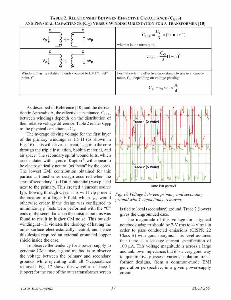
To observe the tendency for a power supply to generate CM noise, a good method is to observe the voltage between the primary and secondary grounds while operating with all Y-capacitance removed. Fig. 17 shows this waveform. Trace 1 (upper) for the case of the outer transformer screen
is tied to local (secondary) ground. Trace 2 (lower) gives the ungrounded case.
The magnitude of this voltage for a typical notebook adapter should be 2-V rms to 4-V rms in order to pass conducted emissions (CISPR 22 Class B) with good margins. This level assumes that there is a leakage current specification of 100 µA. This voltage magnitude is across a large and unknown impedance, but it is a very good way to quantitatively assess various isolation trans-former designs, from a common-mode EMI generation perspective, in a given power-supply circuit.
tAble 2. relAtIonshIp between effectIVe cApAcItAnce (ceff) And physIcAl cApAcItAnce (cg) Versus wIndIng orIentAtIon for A trAnsformer [10]
C C
V
p
nV
p
G 2EFF
CC (1 n
3)n ,= × + +
where n is the turns ratio.
C C
V
p
nV
p
( )2GEFF
CC 1 n
3= −
Winding phasing relative to ends coupled to EMI “quiet” point, C.
Formula relating effective capacitance to physical capaci-tance, CG, depending on voltage phasing:
G 0 rAC d
×ε ×=ε
Time
(
10 µs/div
)
Trace 1
(
2 V/div
)
Trace 2
(
5 V/div
)
Fig. 17. Voltage between primary and secondary ground with Y-capacitance removed.

TexasInstruments 18 SLUP2655-18
Topi
c 5
Adjusting the magnitude and phase of ICM may be used to “tune” the voltage between input ground and output ground to almost zero. Still, this usually does not give optimal EMI control, because the transformer is likely to be compensating for other components and will probably be creating intercomponent current loops that will inductively couple more noise.
Another technique for creating the correct IP-S is to use a coupling foil plate (non-shorted turn) connected to the appropriate potential. This is illustrated in the low-profile transformer design shown in Fig. 18. The design choices led to an entirely wirewound transformer construction in an EFD-type core with primary and secondary wind-ings each on one layer of a bobbin (as shown in Fig. 19). This is a half bridge driven using a scheme similar to that shown in Fig. 15. The difficulty with this low-profile design—where both primary and secondary windings occupy single layers—is that these layers are on average electrostatically neutral and thus do not provide the capacitive-current generator. Conveniently, the gate-driver overwind provided the higher 1.3-H potential that provided optimum EMI by connecting this higher potential to a coupling foil between the primary and secondary. This facilitates the local closing of the capacitive-current generators in the same way that the winding arrangement of Fig. 19 accomplished the task. Note that one must be careful with the connection point to the foil, because it too will have the induced voltage/turn. The center of the turn (i.e., halfway around) is the best place to make the connection. This may be at the top or bottom of the winding layer.
Transformer designs for applications that require very low leakage, such as medical prod-ucts or “no tingle” adapters, will obviously require much more strict attention to interwinding capac-itances. For these critical applications, it may be appropriate to add primary- and/or secondary-referenced shields between the primary and sec-ond ary. A center connection to these shields to create balanced voltage gradients that are in phase is recommended. Foils should be thin (and ideally of higher-resistivity material, such as brass) to reduce eddy loss. As an aside, an alternative is to create a high leakage transformer. One benefit of high leakage inductance in a transformer is that it
6 T
2 T
2 T
1.3 H
–1.3 H
6 T
12 T
C
–Gate Drive Winding (GDB)
+Gate Drive Winding (GDA)
C
2 H
H
–H
ps
pf
Fig. 18. Schematic of alternative adapter transformer.
C
H
Core
–1.3 H
+1.3 H
GDB2 pf
GDA1
GDB1
GDA2 ps
Foil
C
H
Ip-c
Ifoil-p
–H
C
Fig. 19. Transformer winding arrangement with foil plate connected to gate-drive overwind at approximately 1.3-H potential.
TexasInstruments 19 SLUP2655-19
Topi
c 5
will be associated with a low primary-to-secondary capacitance. This will be also be beneficial in creating a low “tingle” adaptor. The LLC topology could benefit from having such high leakage and would be a good choice for applications requiring low leakage to the output. There are also low-magnitude, higher-frequency harmonics in the LLC and hence there should not be a high proximity-loss penalty.
VII. low-profIle flybAck trAnsformer desIgn
A flyback “transformer” (really a coupled inductor) becomes an interesting challenge when a low profile is a requirement.
The magnitude of AC flux—and particularly the AC gap-fringe field—is proportional to mag net-izing current ripple. If minimizing the AC gap field were a primary objective, the choice would be for low-ripple continuous-conduction mode (CCM) as opposed to discontinuous-conduction mode (DCM). Planar windings (sheet area coplanar with the core gap) create a high degree of eddy current loss in low-profile EE-type core structures because they present a large area normal to the gap fringe field, which causes current concentration at the inner edge and therefore greatly increase AC resistance. Low-profile core shapes also tend to have increased leakage between the core top and bottom plates.
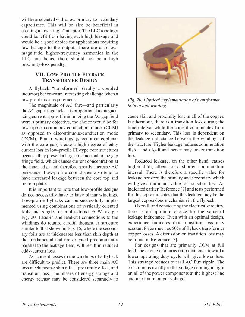
It is important to note that low-profile designs do not necessarily have to have planar windings. Low-profile flybacks can be successfully imple-ment ed using combinations of vertically oriented foils and single- or multi-strand ECW, as per Fig. 20. Lead-in and lead-out connections to the windings do require careful thought. A structure similar to that shown in Fig. 16, where the sec ond-ary foils are at thicknesses less than skin depth at the fundamental and are oriented predominantly parallel to the leakage field, will result in reduced eddy-current loss.
AC current losses in the windings of a flyback are difficult to predict. There are three main AC loss mechanisms: skin effect, proximity effect, and tran si tion loss. The phases of energy storage and energy release may be considered separately to
cause skin and proximity loss in all of the copper. Furthermore, there is a transition loss during the time interval while the current commutates from primary to secondary. This loss is dependent on the leakage inductance between the windings of the structure. Higher leakage reduces commutation dIP/dt and dIS/dt and hence may lower transition loss.
Reduced leakage, on the other hand, causes higher di/dt, albeit for a shorter commutation interval. There is therefore a specific value for leakage between the primary and secondary which will give a minimum value for transition loss. As indicated earlier, Reference [7] and tests performed for this topic indicates that this leakage may be the largest copper-loss mechanism in the flyback.
Overall, and considering the electrical circuitry, there is an optimum choice for the value of leakage inductance. Even with an optimal design, experience indicates that tran si tion loss may account for as much as 50% of flyback transformer copper losses. A discussion on transition loss may be found in Reference [7].
For designs that are primarily CCM at full load, the choice of a turns ratio that tends toward a lower operating duty cycle will give lower loss. This strategy reduces overall AC flux ripple. The constraint is usually in the voltage derating margin on all of the power components at the highest line and maximum output voltage.
Fig. 20. Physical implementation of transformer bobbin and winding.
TexasInstruments 20 SLUP2655-20
Topi
c 5
A key design check with all gapped magnetic components will ensure that local winding hotspot temperatures do not occur near the gap. External winding surface temperatures can be well within ratings while lifetime-degrading temperatures are occurring in the gap-fringe field. As stated previ-ously, thermocouple measurements in a quali fi-cation sample can provide important thermal data.
VIII. low-loss trAnsformer desIgns for moderAte swItchIng frequencIes
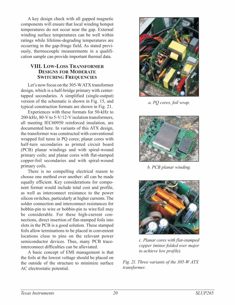
Let’s now focus on the 305-W ATX transformer design, which is a half-bridge primary with center-tapped secondaries. A simplified (single-output) version of the schematic is shown in Fig. 15, and typical construction formats are shown in Fig. 21.
Experiences with these formats for 50-kHz to 200-kHz, 80-V to 5-V/12-V isolation transformers, all meeting IEC60950 reinforced insulation, are documented here. In variants of this ATX design, the transformer was constructed with conventional wrapped foil turns in PQ cores; planar cores with half-turn secondaries as printed circuit board (PCB) planar windings and with spiral-wound primary coils; and planar cores with flat-stamped copper-foil secondaries and with spiral-wound primary coils.
There is no compelling electrical reason to choose one method over another: all can be made equally efficient. Key considerations for compo-nent format would include total cost and profile, as well as interconnect resistance to the power silicon switches, particularly at higher currents. The solder connection and interconnect resistances for bobbin-pin to wire or bobbin-pin to wire/foil may be considerable. For these high-current con-nections, direct insertion of flat-stamped foils into slots in the PCB is a good solution. These stamped foils allow terminations to be placed in convenient locations close to pins on the relevant power semiconductor devices. Thus, many PCB trace-interconnect difficulties can be alleviated.
A basic concept of EMI management is that the foils at the lowest voltage should be placed on the outside of the structure to minimize surface AC electrostatic potential.
Fig. 21. Three variants of the 305-W ATX transformer.
a. PQ cores, foil wrap.
b. PCB planar winding.
c. Planar cores with flat-stamped copper (minor folded over major to achieve low profile).
TexasInstruments 21 SLUP2655-21
Topi
c 5
When considering interleaving from the per-spec tive of primary MMF and the cancelling second ary MMF, the creation of a “sandwich” structure will reduce the field created in the windings. This reduced field in the winding space (leakage field) will result in reduced proximity loss [1]. The trade-off between magnetic loss and circuit loss (with their dependence on the leakage inductance parameter) is complex. Some leakage inductance is to be desired, as it can be used to pro mote resonant transitions. In the flyback mag-netic, it also tends to reduce transition loss. A single triple-sandwich structure of secondary-primary-secondary (S-P-S) gives low loss. More levels of interleaving (for a conventional planar format) provide diminishing overall loss savings.
A further observation is that center-tapped windings are inherently more lossy than the single winding and full-wave rectifier approach, while appreciating the additional diode drop associated with full-wave rectification. Copper losses for a single winding situation can be calculated using the techniques described in Reference [9]. With the center-tapped arrangement, there is always a non-power transferring winding phase exposed to
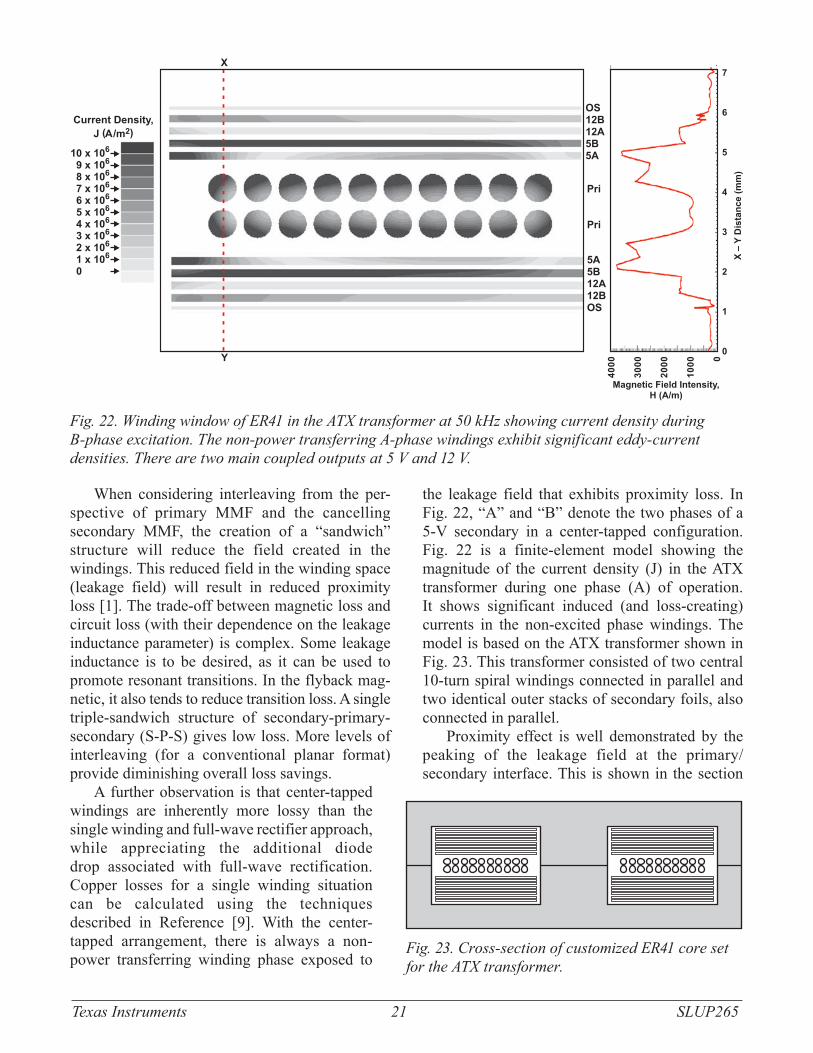
the leakage field that exhibits proximity loss. In Fig. 22, “A” and “B” denote the two phases of a 5-V secondary in a center-tapped configuration. Fig. 22 is a finite-element model showing the magnitude of the current density (J) in the ATX transformer during one phase (A) of operation. It shows significant induced (and loss-creating) currents in the non-excited phase windings. The model is based on the ATX transformer shown in Fig. 23. This trans former consisted of two central 10-turn spiral wind ings connected in parallel and two identical outer stacks of secondary foils, also connected in parallel.
Proximity effect is well demonstrated by the peaking of the leakage field at the primary/ secondary interface. This is shown in the section
10 x 109 x 108 x 10
6
6
6
7 x 106 x 105 x 104 x 103 x 102 x 101 x 100
6
6
6
6
6
6
6
x 106
OS12B12A5B5A
5A5B12A12BOS
7
6
5
4
3
2
1
0
40
00
30
00
20
00
10
00 0
Pri
Pri
Magnetic Field Intensity,H (A/m)
X–
YD
ista
nc
e (
mm
)
Current Density,
J (A/m )2
X
Y
Fig. 22. Winding window of ER41 in the ATX transformer at 50 kHz showing current density during B-phase excitation. The non-power transferring A-phase windings exhibit significant eddy-current densities. There are two main coupled outputs at 5 V and 12 V.
Fig. 23. Cross-section of customized ER41 core set for the ATX transformer.

TexasInstruments 22 SLUP2655-22
Topi
c 5
MMF profile in Fig. 22. Another important idea is to have secondary windings with the greatest NI (transformed cancelling MMF) closest to the primary. Cancelling leakage MMF over the shortest distance will ensure that other secondary windings experience lower MMF and lower loss. Fig. 22 also shows that there will be regions of higher eddy-current loss at foil inside and outside edges where P-S leakage is highest. A final observation based on Fig. 22 is that the winding inside edges, having lower MLT, exhibit greater loss.
Care should be taken to balance losses in sandwich windings with center taps. For example, for an S-P-S sandwich, the order should be SA-SB-P-SB-SA. This symmetrical arrangement (with balanced MMF) gives the lowest overall and instantaneous proximity losses in the foils connected in parallel.
IX. multIple VoltAge trAnsformers
There are many ways to generate multiple out-put voltages from a converter, each with advantages and disadvantages [11]. Computer ATX power supplies have traditionally had two high-power outputs, with typically 60% of the power at 12 V and 40% of the power at 5 V. This requirement was demonstrated to be well satisfied by a tech-nique known as “major-minor” for deriving differ-ent well-coupled voltages. In the ATX transformer implementation, it is relatively straightforward to implement the various necessary design approaches described in this topic.
Computer power-supply requirements may well migrate to a distributed power architecture (DPA), with a main isolated conversion stage providing a single voltage for distribution to downstream point-of-load (POL) power supplies as required. Nevertheless, this section shows the flexibility of magnetic solutions in generating multiple different voltages efficiently.
A. Major-Minor ApproachThe most practical (conventional) transformer
for a multi-output-voltage (e.g., 12-V and 5-V) power supply employing integer numbers of turns may have something like a 7:3 secondary turns ratio. For this example, there are 1.67 V/turn (5 V divided by three turns). This is not well suited to real-world cost considerations, however, and also results in an inefficient usage of ferrite material. Cores with flux levels corresponding to 5 V/turn are considerably more cost-effective and result in materially lower conduction loss. For this example, it would be ideal if the 5-V winding were to have a single turn.
A series connection of two cores, each operat-ing at different volts per turn, is an alternative way to achieve coupling to a winding with a non-integer multiple of volts per turn. The idea (see Fig. 24) is that a high-current winding may be one turn and an extension of this winding through another “minor” core may add or subtract a non-integer multiple of the voltage picked up by the winding portion through the “major” core. Each of the cores is supporting a different number of volts per turn.
For this example, the high-current 5-V winding is a single turn. The 12-V output is derived by having an extra turn on the main winding to give a 10-V level, again in the bi-phase (center-tapped) approach associated with double-ended power conversion. This needs to be augmented by adding a further level of 2 V to each phase. The 2 V comes from a single-turn secondary on the minor transformer, which operates at 2 V/turn. The primary of the minor transformer is driven across the A and B phases of the 5 V to give 10 V. A minor transformer with a 5:1 turns ratio is then consistent with generating the 2 V.
This approach can work very effectively and has been proven to be consistent with very high efficiency at low cost. The volts-per-turn figure for the minor transformer is 2 V/turn, and thus for similar core loss an area 40% of that of the main transformer can be used. This results in a core volume that is typically 25% of the larger core.

TexasInstruments 23 SLUP2655-23
Topi
c 5
The multiple-core approach allows single or even half turns to minimize copper loss and can allow clever circuit interconnect structures.
The schematic for this example approach is shown in Fig. 24.
It is usually desirable to get low leakage between the two phases of a winding, which can reduce the level of voltage “spiking” during transi-tions and accordingly reduce clamp losses. This is
typically achieved by placing the windings in very close proximity, with maximum overlap. However, EMI will be a consideration as leakage is reduced.
An important advantage of the major-minor approach is that it facilitates single-turn foil secondaries. These may then be arranged as discussed earlier for symmetrical MMF profiles such that this again tends to give a copper-loss advantage.
tAble 3. foIl/wIndIng structure formIng the VertIcAl stAck wIthIn the AtX trAnsformer wIndow
12B 12A 5B 5A P P 5A 5B 12A 12B
Primary
0 V
5 V
12 V
++
1 1
1T
1T
1T
1T
10T
5B5A
12B12A
5T Minor
Primary
Major Core
Minor
Core
Fig. 24. Schematic of the center-tapped, major-minor transformer approach.

TexasInstruments 24 SLUP2655-24
Topi
c 5
When a planar core combined with stamped copper foils for the secondary windings is used, the primary windings must fit into a very low-profile window. Producing the windings in a spiral arrangement is very suitable for this (see Fig. 25). Voltage isolation is easily achieved through the use of triple-insulated wire for the primary winding. The planar ER41 core chosen has a window width of 10.82 mm. As a 10-turn winding is required, 0.7-mm, triple-insulated copper proved suitable. Two of the primary coils were connected in parallel to minimize the DC resistance. This winding structure, consisting of the 0.2-mm-thick foils and the 0.7-mm-diameter primary windings in ER41 planar cores, yielded copper dissipation in the major transformer of approximately 1.7 W for a 305-W output.
The transformer was implemented using the secondary foils shown in Fig. 26. The terminations are directly soldered into PTH slots in the mother-board (Fig. 25b). The shapes and outlines of these prototype foils do not represent a final high-volume design, which would involve a further analysis of conduction loss as well as material, manufacturing, and assembly costs.
The primary coil of the minor transformer consists of five turns wound on a customized EQ25 bobbin. The secondaries for the minor are the center/upper sections of the 12A and 12B foils. The minor transformer assembly is completed with EQ25 and EQ25LP core halves. A typical major-minor transformer configuration is shown in Fig. 27.
This technique for generating multiple voltages is fundamentally applicable to many situations. Con sid erations for multiple cores versus multiple turns are as much mechanical as electrical. No significant electrical drawbacks were uncovered with this approach. The idea could be very appropriate for highly integrated or highly automated magnetic constructions.
X. desIgn for mAnufActurAbIlIty And repeAtAbIlIty
A major constraint on the design and implementation of any power magnetic device is that it be manufacturable, with repeatable char ac-ter istics, and that it can be easily assembled into the application at the required cost. In practice, this means that the design must be implemented
Power Silicon
Foil Terminations
Fig. 25. Assembly of the ATX transformer and insertion into application PCB.
a. One half of transformer showing two primary coils in parallel, with center termination brought out along a groove (hidden) in the core face.
b. Proximity of terminations of the direct inserted secondary foils to the output rectifiers, 305 W ATX
TexasInstruments 25 SLUP2655-25
Topi
c 5
with readily available material sets using common manufacturing techniques and with a minimum number of assembly operations.
For transformers with safety implications, creep age/clearance requirements can be addressed either by margin tape, triple-insulated wire, or a specially constructed bobbin, with the material system being a UL-approved insulation system. For high-density designs, the use of margin tape or special bobbins results in a very inefficient use of the winding window area. Some high-volume designs have successfully integrated either the primary or ancillary windings (gate drive, bias, cancellation) into a multilayer PCB with suitable copper-to-edge clearance. The elimination of “flying” wires is a valuable byproduct of such a scheme. This mixed PCB and wound construction methodology gives a good balance of low-cost assembly and high repeatability.
The use of foil windings is common (especially for lower-voltage, higher-current outputs), with the main issue being suitable and reliable high-current terminations between the foil and the PCB. Foil foldovers tend to be fragile, while multiple foils with a bend can lead to unacceptable mechanical tolerance issues with the assembly. A foil thickness of 0.2 mm achieves a practical combination of mechanical stiffness and high current capability, combined with acceptable thickness from a skin-depth point of view for switching square waves up to 200 kHz. The multi-output ATX transformer described in this topic uses secondary foil stacks with foils shaped to allow direct insertion and soldering into the application motherboard without any bending or folding operations. Individual foils shaped to allow PCB terminations can aid optimal component placement (proximity to power silicon). The foils can be shaped to remove unnecessary copper, to allow low-cost stamping operations, and to aid/ease mechanical assembly operations.
The use of semicustom core shapes as shown in Fig. 28 can be very beneficial: slots/cutouts can be specified to accommodate leadouts or specially shaped bob bins, especially for high-density designs. However, any additional cost or logistical impli-cations need to be carefully established; they may vary significantly for different manufacturing facilities.
Fig. 28. Customized EQ25 core with slots to allow ingress and egress of primary windings.
5A 5B
12A 12B
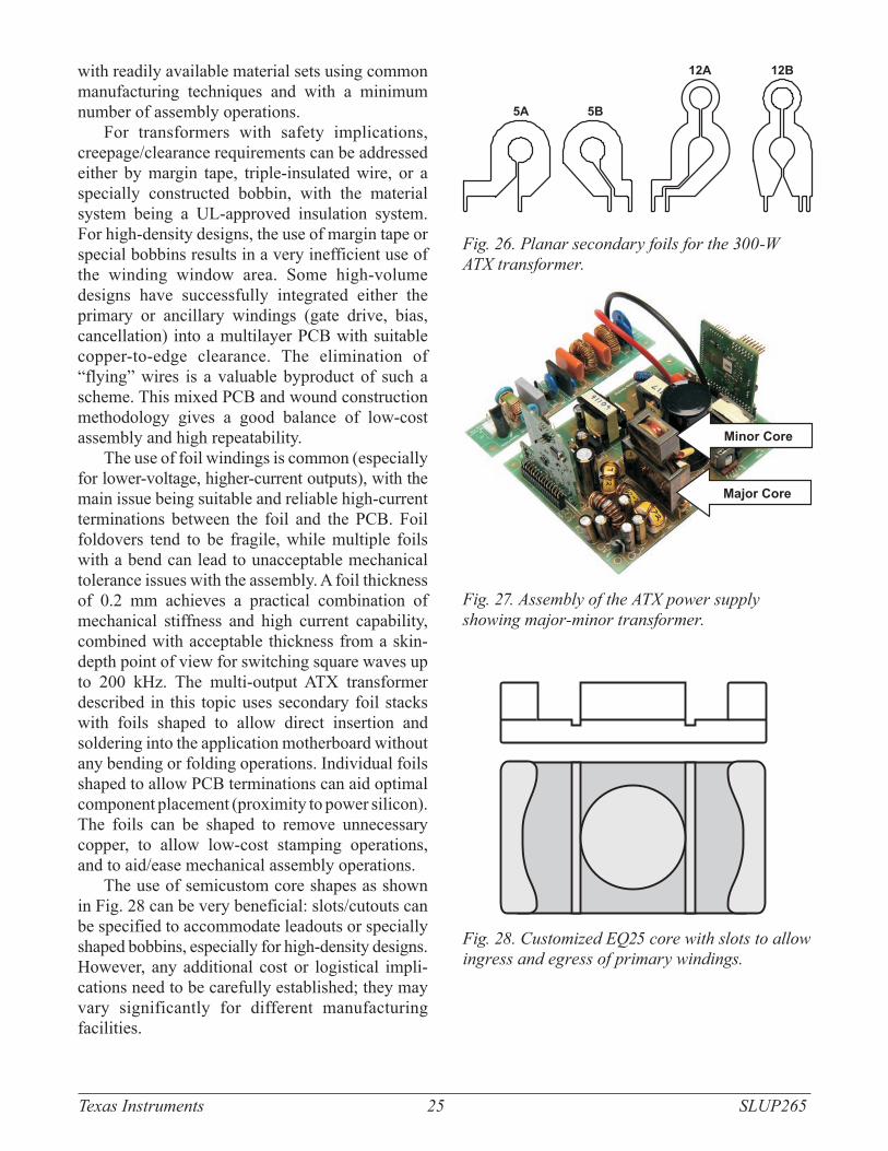
Fig. 26. Planar secondary foils for the 300-W ATX transformer.
Minor Core
Major Core
Fig. 27. Assembly of the ATX power supply showing major-minor transformer.

TexasInstruments 26 SLUP2655-26
Topi
c 5
XI. eXperIences wIth pArAlleled hAlf-turn wIndIngs
One of the efficiency goals was to use single-turn secondary windings where possible. However, there are situations when fractional turns (less than one full turn) are required. Many of these are listed in Reference [1].
For planar PCB windings in particular, it may be worthwhile to consider parallel half-turn windings for high current. A half-turn winding is actually a full turn around half of the total flux, which could be accomplished in an EE-type core with a full turn around one of the outer legs. Paralleling two such half turns will give very low DC resistance.
Perfect balance and symmetry of these wind-ings and the electrical circuits that they complete is necessary. This is to ensure that the outer leg AC fluxes and associated volts per turn are balanced.
As well as achieving AC flux balance between the outer legs, there must also be a perfect DC voltage balance between the outer windings and their circuits. Commutation mismatches between outer-leg circuits or variations in semiconductor resistances can cause a mismatch in net DC volts per turn between the outer legs. This DC mismatch may cause a DC flux to flow in the outer legs only (substantially equal and opposite) even while still maintaining zero DC flux in the center leg. DC fluxes in the outer legs would lead to staircase saturation in the outer legs. Technically, these DC fluxes could be supported by having gaps in the outer legs, but practically, equal gaps across all three legs is best to prevent this flux saturation, even at the expense of increased magnetizing current. The conclusion is that there is more moti-va tion for introducing a gap to the transformer structure in the case of paralleled half turns.
XII. references
[1] Lloyd Dixon, “Magnetics Design Handbook - MAG100A,” [Online]. Available: www-s.ti.com/sc/techzip/slup222.zip
[2] J. E. Brittain, “A Steinmetz Contribution to the AC Power Revolution,” Proceedings of the IEEE, Vol. 72, No. 2, pp. 196–197, Feb. 1984.
[3] S. Mulder, “Power Ferrite Loss Formulas for Transformer Design,” Power Conversion and Intelligent Motion, Vol. 21, No. 7, pp. 22–31, July 1995.
[4] E.C. Snelling, Soft Ferrites: Properties and Applications, 2nd ed.: Butterworth-Heinemann, 1988.
[5] A. Nace and R. Ridley, “Modeling Ferrite Core Losses,” Switching Power Magazine, Vol. 3, No. 1, pp. 6–13, 2002.
[6] Ferroxcube, Soft Ferrites and Accessories, 2005 Data Handbook [Online]. Available: http://www.ferroxcube.com/appl/info/HB2009.pdf
[7] C.R. Sullivan, T. Abdallah, and T. Fujiwara, “Optimization of a Flyback Transformer Winding Considering Two-Dimensional Field Effects, Cost and Loss,” IEEE Applied Power Electronics Conference (APEC), pp. 142–150, March 2001.
[8] J. Schneider and G. Young, “Integral Cycle Control Techniques for High-Efficiency Power Conversion,” Proceedings of PCIM Europe, 2009.
[9] W.G. Hurley, E. Gath, and J.G. Breslin, “Optimizing the AC Resistance of Multilayer Transformer Windings with Arbitrary Current Waveforms,” IEEE Trans. on Power Elec tron-ics, Vol. 15, No. 2, pp. 369–376, March 2000.
[10] I. Jitaru, “Planar Magnetics Technologies—Seminar 6,” IEEE Applied Power Electronics Conference (APEC), 2000.
[11] R. Ridley, “Ways to Generate Multiple Outputs,” Switching Power Magazine, Vol. 4, No. 2, pp. 6–21, 2003.
[12] V. Quinn, “Expert Shortcuts to More Effective Transformer Design—Seminar 18,” IEEE Applied Power Electronics Conference (APEC), 2006.
[13] E. Bennett, Sidney C. Larson, “Effective Resistance of Multilayer Windings,” AIEE Transactions, vol.59, pp. 1010-1016, 1940
[14] Dr. Ray Ridley, “Proximity Loss in Magnetics Windings,” Designer Series XIII, [Online]. Available: www.switchingpowermagazine.com/downloads/13 Proximity Loss.pdf

TexasInstruments 27 SLUP2655-27
Topi
c 5
AppendIX A. derIVAtIon of InterwIndIng cApAcItAnce
a c
b
d
dx
w x
Vx
V
x
V
bd
V
ac
Fig. A-1. Winding variables.
Reference [10] contains a treatment for the derivation of interwinding and intrawinding effective capacitances for some winding and layer structures. With Fig. A-1 used as a reference, the derivation of interwinding capacitance is as follows. The potential difference at element dx is
x bd ac bdx
V V )(V V .w
×= + −
The associated electrostatic energy is2
G bd ac bd1 dx x
dU C V (V V2 w w
) . = × × + − ×
Integration across the winding width, w, gives the total energy as
2 2G bd acd acb
1U C (V V V V .
6)= × × + +×
ANSYS and Maxwell are registered trademarks of ANSYS, Inc. Kapton is a registered trademark of DuPont.

TI Worldwide Technical Support
InternetTI Semiconductor Product Information Center Home Pagesupport.ti.com
TI E2E™ Community Home Pagee2e.ti.com
Product Information CentersAmericas Phone +1(972)644-5580
Brazil Phone 0800-891-2616
Mexico Phone 0800-670-7544
Fax +1(972)927-6377 Internet/Email support.ti.com/sc/pic/americas.htm
Europe, Middle East, and AfricaPhone EuropeanFreeCall 00800-ASK-TEXAS (0080027583927) International +49(0)8161802121 RussianSupport +7(4)959810701
Note:TheEuropeanFreeCall(TollFree)numberisnotactiveinallcountries.Ifyouhavetechnicaldifficultycallingthefreecallnumber,pleaseusetheinternationalnumberabove.
Fax +(49)(0)8161802045Internet support.ti.com/sc/pic/euro.htmDirectEmail [email protected]
JapanPhone Domestic 0120-92-3326
Fax International +81-3-3344-5317 Domestic 0120-81-0036
Internet/Email International support.ti.com/sc/pic/japan.htm Domestic www.tij.co.jp/pic
AsiaPhone International +91-80-41381665 Domestic Toll-FreeNumber Note:Toll-freenumbersdonotsupport
mobileandIPphones. Australia 1-800-999-084 China 800-820-8682 HongKong 800-96-5941 India 1-800-425-7888 Indonesia 001-803-8861-1006 Korea 080-551-2804 Malaysia 1-800-80-3973 NewZealand 0800-446-934 Philippines 1-800-765-7404 Singapore 800-886-1028 Taiwan 0800-006800 Thailand 001-800-886-0010Fax +8621-23073686Email [email protected]@ti.comInternet support.ti.com/sc/pic/asia.htm
A122010
Important Notice:TheproductsandservicesofTexasInstrumentsIncorporatedanditssubsidiariesdescribedhereinaresoldsubjecttoTI’sstandardtermsandconditionsofsale.CustomersareadvisedtoobtainthemostcurrentandcompleteinformationaboutTIproductsandservicesbeforeplacingorders.TIassumesnoliabilityforapplicationsassistance,customer’sapplicationsorproductdesigns,softwareperformance,orinfringementofpatents.Thepublicationofinformationregardinganyothercompany’sproductsorservicesdoesnotconstituteTI’sapproval,warrantyorendorsementthereof.
TheplatformbarandE2EaretrademarksofTexasInstruments.Allothertrademarksarethepropertyoftheirrespectiveowners.
SLUP265

IMPORTANT NOTICE
Texas Instruments Incorporated and its subsidiaries (TI) reserve the right to make corrections, modifications, enhancements, improvements,and other changes to its products and services at any time and to discontinue any product or service without notice. Customers shouldobtain the latest relevant information before placing orders and should verify that such information is current and complete. All products aresold subject to TI’s terms and conditions of sale supplied at the time of order acknowledgment.
TI warrants performance of its hardware products to the specifications applicable at the time of sale in accordance with TI’s standardwarranty. Testing and other quality control techniques are used to the extent TI deems necessary to support this warranty. Except wheremandated by government requirements, testing of all parameters of each product is not necessarily performed.
TI assumes no liability for applications assistance or customer product design. Customers are responsible for their products andapplications using TI components. To minimize the risks associated with customer products and applications, customers should provideadequate design and operating safeguards.
TI does not warrant or represent that any license, either express or implied, is granted under any TI patent right, copyright, mask work right,or other TI intellectual property right relating to any combination, machine, or process in which TI products or services are used. Informationpublished by TI regarding third-party products or services does not constitute a license from TI to use such products or services or awarranty or endorsement thereof. Use of such information may require a license from a third party under the patents or other intellectualproperty of the third party, or a license from TI under the patents or other intellectual property of TI.
Reproduction of TI information in TI data books or data sheets is permissible only if reproduction is without alteration and is accompaniedby all associated warranties, conditions, limitations, and notices. Reproduction of this information with alteration is an unfair and deceptivebusiness practice. TI is not responsible or liable for such altered documentation. Information of third parties may be subject to additionalrestrictions.
Resale of TI products or services with statements different from or beyond the parameters stated by TI for that product or service voids allexpress and any implied warranties for the associated TI product or service and is an unfair and deceptive business practice. TI is notresponsible or liable for any such statements.
TI products are not authorized for use in safety-critical applications (such as life support) where a failure of the TI product would reasonablybe expected to cause severe personal injury or death, unless officers of the parties have executed an agreement specifically governingsuch use. Buyers represent that they have all necessary expertise in the safety and regulatory ramifications of their applications, andacknowledge and agree that they are solely responsible for all legal, regulatory and safety-related requirements concerning their productsand any use of TI products in such safety-critical applications, notwithstanding any applications-related information or support that may beprovided by TI. Further, Buyers must fully indemnify TI and its representatives against any damages arising out of the use of TI products insuch safety-critical applications.
TI products are neither designed nor intended for use in military/aerospace applications or environments unless the TI products arespecifically designated by TI as military-grade or "enhanced plastic." Only products designated by TI as military-grade meet militaryspecifications. Buyers acknowledge and agree that any such use of TI products which TI has not designated as military-grade is solely atthe Buyer's risk, and that they are solely responsible for compliance with all legal and regulatory requirements in connection with such use.
TI products are neither designed nor intended for use in automotive applications or environments unless the specific TI products aredesignated by TI as compliant with ISO/TS 16949 requirements. Buyers acknowledge and agree that, if they use any non-designatedproducts in automotive applications, TI will not be responsible for any failure to meet such requirements.
Following are URLs where you can obtain information on other Texas Instruments products and application solutions:
Products Applications
Audio www.ti.com/audio Communications and Telecom www.ti.com/communications
Amplifiers amplifier.ti.com Computers and Peripherals www.ti.com/computers
Data Converters dataconverter.ti.com Consumer Electronics www.ti.com/consumer-apps
DLP® Products www.dlp.com Energy and Lighting www.ti.com/energy
DSP dsp.ti.com Industrial www.ti.com/industrial
Clocks and Timers www.ti.com/clocks Medical www.ti.com/medical
Interface interface.ti.com Security www.ti.com/security
Logic logic.ti.com Space, Avionics and Defense www.ti.com/space-avionics-defense
Power Mgmt power.ti.com Transportation and Automotive www.ti.com/automotive
Microcontrollers microcontroller.ti.com Video and Imaging www.ti.com/video
RFID www.ti-rfid.com
OMAP Mobile Processors www.ti.com/omap
Wireless Connectivity www.ti.com/wirelessconnectivity
TI E2E Community Home Page e2e.ti.com
Mailing Address: Texas Instruments, Post Office Box 655303, Dallas, Texas 75265Copyright © 2011, Texas Instruments Incorporated
Related Documents