1 Optical properties and phase-change transition in Ge 2 Sb 2 Te 5 flash evaporated thin films studied by temperature dependent spectroscopic ellipsometry J. Orava 1* , T. Wágner 1 , J. Šik 2 , J. Přikryl 1 , L. Beneš 3 , M. Frumar 1 1 Department of General and Inorganic Chemistry, Faculty of Chemical Technology, University of Pardubice, Cs. Legion’s Sq. 565, Pardubice, 532 10 Czech Republic 2 ON Semiconductor Czech Republic, R&D Europe, 1. máje 2230, Rožnov pod Radhoštěm, 756 61 Czech Republic 3 Joint Laboratory of Solid State Chemistry of the Institute of Macromolecular Chemistry AS CR, v.v.i. and University of Pardubice, Studentská 84, Pardubice, 53210 Czech Republic * Corresponding author: tel.: +420 466 037 220, fax: +420 466 037 311 * E-mail address: [email protected] Keywords: Ge 2 Sb 2 Te 5 , optical properties, ellipsometry, amorphous, fcc PACs: 07.60.Fs, 77.84.Bw, 78.20.-e, 78.20.Bh Abstract We studied the optical properties of as-prepared (amorphous) and thermally crystallized (fcc) flash evaporated Ge 2 Sb 2 Te 5 thin films using variable angle spectroscopic ellipsometry in the photon energy range 0.54 - 4.13 eV. We employed Tauc-Lorentz model (TL) and Cody- Lorentz model (CL) for amorphous phase and Tauc-Lorentz model with one additional Gaussian oscillator for fcc phase data analysis. The amorphous phase has optical bandgap energy E g opt = 0.65 eV (TL) or 0.63 eV (CL) slightly dependent on used model. The Urbach edge of amorphous thin film was found to be ~ 70 meV. Both models behave very similarly and accurately fit to the experimental data at energies above 1 eV. The Cody-Lorentz model is more accurate in describing dielectric function in the absorption onset region. The thickness decreases ~ 7 % toward fcc phase. The bandgap energy of fcc phase is significantly lower than amorphous phase, E g opt = 0.53 eV. The temperature dependent ellipsometry revealed crystallization in the range 130 - 150 °C. The bandgap energy of amorphous phase possesses temperature redshift -0.57 meV/K (30 - 110 °C). The crystalline phase has more complex bandgap energy shift, firstly +0.62 meV/K (150 - 180 °C) followed by -0.29 meV/K (190 -

Welcome message from author
This document is posted to help you gain knowledge. Please leave a comment to let me know what you think about it! Share it to your friends and learn new things together.
Transcript

1
Optical properties and phase-change transition in Ge2Sb2Te5 flash evaporated thin films
studied by temperature dependent spectroscopic ellipsometry
J. Orava1*, T. Wágner1, J. Šik2, J. Přikryl1, L. Beneš3, M. Frumar1
1Department of General and Inorganic Chemistry, Faculty of Chemical Technology,
University of Pardubice, Cs. Legion’s Sq. 565, Pardubice, 532 10 Czech Republic 2ON Semiconductor Czech Republic, R&D Europe, 1. máje 2230, Rožnov pod Radhoštěm,
756 61 Czech Republic 3Joint Laboratory of Solid State Chemistry of the Institute of Macromolecular Chemistry AS
CR, v.v.i. and University of Pardubice, Studentská 84, Pardubice, 53210 Czech Republic
*Corresponding author: tel.: +420 466 037 220, fax: +420 466 037 311 *E-mail address: [email protected]
Keywords: Ge2Sb2Te5, optical properties, ellipsometry, amorphous, fcc
PACs: 07.60.Fs, 77.84.Bw, 78.20.-e, 78.20.Bh
Abstract
We studied the optical properties of as-prepared (amorphous) and thermally crystallized
(fcc) flash evaporated Ge2Sb2Te5 thin films using variable angle spectroscopic ellipsometry in
the photon energy range 0.54 - 4.13 eV. We employed Tauc-Lorentz model (TL) and Cody-
Lorentz model (CL) for amorphous phase and Tauc-Lorentz model with one additional
Gaussian oscillator for fcc phase data analysis. The amorphous phase has optical bandgap
energy Egopt = 0.65 eV (TL) or 0.63 eV (CL) slightly dependent on used model. The Urbach
edge of amorphous thin film was found to be ~ 70 meV. Both models behave very similarly
and accurately fit to the experimental data at energies above 1 eV. The Cody-Lorentz model is
more accurate in describing dielectric function in the absorption onset region. The thickness
decreases ~ 7 % toward fcc phase. The bandgap energy of fcc phase is significantly lower than
amorphous phase, Egopt = 0.53 eV. The temperature dependent ellipsometry revealed
crystallization in the range 130 - 150 °C. The bandgap energy of amorphous phase possesses
temperature redshift -0.57 meV/K (30 - 110 °C). The crystalline phase has more complex
bandgap energy shift, firstly +0.62 meV/K (150 - 180 °C) followed by -0.29 meV/K (190 -
2
220 °C). The optical properties of as-prepared and fcc flash evaporated Ge2Sb2Te5 thin films
are very similar to those previously reported for sputtered thin films.
1. Introduction
The chalcogenide Ge2Sb2Te5 thin film alloys are commercially used in optical phase
change data storage media (DVD, blue-ray discs) and non-volatile phase change memories
[1]. The wide application in DVD technology is mainly due to the fast phase change transition
(~ 50 ns), highly repeatable cycles over 106 times and long lifetime of amorphous phase ~ 200
years. The main advantages of non-volatile phase change memories are fast programming
time (< 10 ns), long-term data storage endurance exceeding 1013 programming operations and
low voltage programming capability. This material is also very interesting in the field of
cognitive computing [2]. Despite of the superior properties of Ge2Sb2Te5 there are other
potential materials, which could be used in the field of the phase change memory materials
[3]. The Ge2Sb2Te5 thin films are predominantly prepared by sputtering techniques, where
structural [4], optical [5, 6] and electronic properties [7] have been widely investigated. The
Ge2Sb2Te5 thin films are regarded as p-type narrow-gap degenerated semiconductors, where
the hole concentration increases toward crystalline phase [7]. As far as the authors know, no
papers focused on ellipsometry study of flash evaporated Ge2Sb2Te5 thin films have been
published yet.
In this paper we present the optical function spectra of flash evaporated as-prepared
(amorphous) and annealed (thermally crystallized, i.e., face-centered-cubic phase fcc)
Ge2Sb2Te5 thin films. The optical properties are studied by variable angle spectroscopic
ellipsometry (VASE). We employed Tauc-Lorentz (amorphous and fcc) and/or Cody-Lorentz
(amorphous) models to fit the optical parameters of studied films. The parameterization of
models is also presented. We will show that the Tauc-Lorentz model with one additional
Gaussian oscillator is well sufficient to describe the optical properties of crystalline
Ge2Sb2Te5 thin films. The temperature dependent ellipsometry was done to detect the phase
change transition (amorphous to crystalline) and corresponding change of optical properties
upon heating.
2. Experimental
Ge2Sb2Te5 thin films with thickness ~ 200 nm were deposited from powdered bulk sample
(grain size ≤ 0.4 mm) onto cleaned oxide glass substrates using flash evaporation technique
(FE), which was developed at our laboratories. Deposition rate was kept at 0.3 nm/s and a

3
residual pressure of ~ 10-4 Pa. The crystalline phase was obtained by heating of the as-
prepared films for 2 hours at 200 °C in N2 atmosphere to avoid any surface oxidation.
The optical function spectra of the studied as-prepared and thermally crystallized thin
films were evaluated from data measured using VASE® J. A. Woollam Co., Inc. ellipsometer
with automatic rotating-analyzer (RAE) in the photon energy range from 0.54 to 4.13 eV, i.e.,
photon wavelengths 2300 - 300 nm, at angles of incidence 60°, 65° and 70°. The spectra were
measured after 25 nm steps and the acquisition took about 30 minutes. The ellipsometer is
equipped with AutoRetarder®, which allows the measurement of the ellipsometric parameter
Δ at a 360° interval. The temperature dependent spectral ellipsometry was measured in the N2
ambient in the temperature range 30 - 220 °C (303 - 493 K) in 10 °C step (around the
crystallization with 5 °C steps). The sample was placed into HTC-100 heat cell developed by
J. A. Woollam Co., Inc. and the spectra were taken throughout fused silica windows at fixed
angle of incidence 70°. The phase change (PC) transition upon different heating rates (1 - 5
°C/min) was detected at one wavelength λ = 1700 nm (~ 0.73 eV), which is close to the
optical bandgap energy of amorphous material and was found to be very sensitive for PC
transition. The PC was done in the temperature range 30 - 200 °C.
X-ray diffraction data of thermally crystallized samples were obtained with a D8-Advance
diffractometer (Bruker AXE, Germany) using CuKα radiation with secondary graphite
monochromator.
AFM measurements were realized on Solver Pro M Atomic Force Microscope (NT-MDT;
Russia) operating in semi-contact mode. The high-resolution „Golden“ silicon cantilevers
NSG-10 (Au coating, cone angle less than 22° and typical cantilever spring constant 11.5
N.m-1) were used for all measurements. The images were recorded at engaged oscillation 50
% of free oscillation, scan frequency between 0.5 and 1 Hz for a resolution 256 x 256 pixel.
The smoothness (Sa) was calculated according to ISO 4287-1997.
3. Theory
3.1 Spectroscopic Ellipsometry
Spectroscopic ellipsometry (SE) is known as an effective technique for determination of
optical function spectra of variety of materials. The SE spectra are represented by traditional
ellipsometry parameters Ψ and Δ, which denote the amplitude ratio and phase shift of
perpendicularly polarized waves after their reflection off the surface of studied sample [8, 9].
The Ψ and Δ could be directly detected in nulling ellipsometry as an azimuthal angle of the
4
analyzer and polarizer at which the light intensity is minimal at the detector [8]. In RAE the
time dependent flux I(t) incident on detector for fixed polarizer element varies according to:
I(t) = I0[1 + αcos2A(t) + βsin2A(t)], (1)
A(t) = 2πf0t + θ, (2)
where I0 is the average intensity, α and β the normalized Fourier coefficients describing the
phase and relative amplitude of the ac component of the flux incident on the detector. The
Fourier coefficients α and β are measured in RAE. A represents immediate analyzer azimuth
angle measured with respect to a zero reference. The A is a harmonic function of time, since
the analyzer is rotating continuously. f0 is an optical frequency, which equals to twice a
mechanical rotation frequency and θ is an arbitrary constant phase factor [10]. If the detector
signal is measured as function of time [Eqns. (1) and (2)] then the Fourier coefficients α and β
of the signal could be obtained and the Ψ and Δ ellipsometry parameters in RAE calculated as
follows
ΦΨΦΨα 22
22
tantantantan
+−
= , (3)
ΦΨΦΔΨβ 22 tantan
tancostan2+
= , (4)
Φ−+
=Ψ tan11tan
αα , (5)
21cos
αβΔ−
= , (6)
where Ф stands for polarizer azimuthal angle [11].
A common representation of the SE data Ψ and Δ is a complex pseudodielectric function
<ε> = <ε1>+i<ε2>, which eliminates the angle of incidence dependence of Ψ and Δ [12].
a2
a2
a2
2
a2
21 tancossin11Ni Φ
Φ+Φ
ρ+ρ−
ε=>>=<ε<+>ε>=<ε< , (7)

5
where N represents pseudocomplex refractive index. εa is the ambient dielectric function and
equals 1 in case of air. An angle of incidence is denoted as Фa. The complex pseudodielectric
function <ε> equals complex dielectric function ε only if ellipsometric data Ψ and Δ are
measured from a bulk material with no layer on the top.
SE is an indirect technique and a model calculation is needed for sample analysis.
Calculated model spectra are fitted to the experimental data by varying model parameters.
Our model included surface roughness, thin film and oxide glass substrate. We did not
involve any surface oxide layer into our models. As effective medium models are often used
for modeling of microscopic surface roughness in spectroscopic ellipsometry [13], we
modeled surface roughness by using the Bruggeman effective medium approximation (EMA),
i.e., the surface layer consisting from the same bulk material with void density of 50 % [14].
The optical properties of bulk oxide glassy substrate were evaluated separately to reduce
number of unknown parameters in the entire model. The Cauchy formula [9] was used to
obtain a long-wavelength refractive index 1.4933 and curvature of refractive index toward
higher energies 0.0083 in the entire spectral region, i.e., 300 - 2300 nm. The optical
parameters of glassy substrate were kept constant during modeling process. We also did not
include any correction to the free carrier absorption in this material, which gets significant at
energies below measured region [15].
The number of unknown parameters for data analysis can be greatly reduced if an
appropriate parameterization of optical functions, i.e., model dielectric functions (MDFs), is
available for the materials of interest. A regression analysis is then used to differentiate the
model parameters until the calculated ( Ψimod and Δi
mod) and measured data ( Ψiexp and Δi
exp)
match as closely as possible. This is performed by minimizing the mean square error function
(MSE), which is appropriately weighted to the estimated experimental errors ( σΨ,iexp and
σΔ,iexp).
∑= ∆ψ
σ∆−∆
+
σψ−ψ
−=
N
1i
2
expi,
expi
modi
2
expi,
expi
modi
MN21MSE . (8)
The number of measured ψ and Δ pairs is N and the total number of real valued fit parameters
is M. For detailed information on the principal of ellipsometry we refer to [8, 9 and 11].
3.2 MDFs (model dielectric functions) of FE Ge2Sb2Te5 thin films

6
The optical functions are usually in the form of a complex dielectric function ε = ε1 + iε2
or a complex refractive index N = n + ik, where n is refractive index (real part) and k
extinction coefficient (imaginary part) and ε = N2 Eq. (7). The real and imaginary part of
complex dielectric function and refractive index are connected throughout ε1 = n2 - k2 and ε2
= 2nk. We used two following dispersion models, i.e., Tauc-Lorentz (TL) [16, 17] and Cody-
Lorentz (CL) [18] to obtain optical functions of the studied samples in the entire measured
region. One additional Gaussian oscillator (Gosc) [11] was added into TL model to describe
the more pronounced structure of dielectric function of crystalline sample. The above
mentioned models (TL, TL + Gosc) were also used to evaluate the varying of optical function
spectra of Ge2Sb2Te5 thin films in dependence on temperature [19].
The Tauc-Lorentz model
The Tauc-Lorentz (TL) oscillator model developed by Jellison and Modine [16, 17] was
used to describe the optical functions of amorphous films in the entire measured spectral
region. Using the same model with additional Gaussian oscillator (TL+Gosc) we obtained the
optical functions of the studied fcc Ge2Sb2Te5 thin films. We also made a report on the
oscillator parameters extracted from TL model. The ε2 imaginary part of dielectric function
according to the TL model is obtained by taking into account Tauc joint density of states [20],
Lorentz oscillator [11] and Forouhi and Bloomer formalism [21, 22] of optical function. The
following dispersion is obtained
)E(L)E(GEC)EE(
EACE.E
)EE(nk2)E( 2222
02
02
2optg
TL2 =+−
−==ε . (9)
G(E) and L(E) represent variable band-edge function and Lorentz oscillator function,
respectively. The G(E) represents here the Tauc law, i.e., ħω2ε2 ~ (ħω - Egopt)2. The
parameters in Eq. (9) are amplitude (oscillator strength) A, peak transition energy E0, optical
bandgap energy Egopt and broadening C. The Eq. (9) is used in the range of energies E > Eg
opt.
ε2Tauc-Lorentz is 0 in the range of energies E ≤ Egopt, i.e., below optical bandgap energy. This
model contains only interband transitions. Some defects and/or intraband transitions are not
included in this model. The real part of dielectric function ε1 is calculated by the Kramers-
Kronig integration formula

7
∫∞
−+∞=
optgE
222
11 dE
)(P2)()E( ξξ
ξξεπ
εε , (10)
where P stands for the Cauchy principal part of the integral. ε1(∞) is a fitting parameter in the
model and represents constant contribution to ε1 at high energies beyond the measured
spectral region. The integral could be solved in the closed form which is shown elsewhere [16,
17].
The Cody-Lorentz model
The Cody-Lorentz (CL) oscillator model was developed by Ferlauto et al. [18]. It is
similar to TL in the way that it defines Egopt and Lorentz absorption peak. However the G(E)
behaves differently in the absorption onset region and Urbach absorption term is also
included.
>+−+−
−=
≤<
−
=ε
,EE;EC)EE(
EACE.E)EE(
)EE()E(L)E(G
EE0;E
EEexpEE
t22220
20
2p
2optg
2optg
tu
t1
CL2
where Et is the boundary between Urbach tail transition, which forms the top of valence band
and the band-to-band transition. In Eq. (11a) the expression for 0 < E ≤ Et leads to the Urbach
form of the absorption coefficient, i.e., α(E) ~ exp(E/Eu) [23]. Eu is corresponding weak
Urbach absorption energy. The E1 is defined so that ε2CL(E) is continuous at E = Et; thus E1 =
EtL(Et)G(Et). Ep in Eq. (11) defines a second transition energy (in addition to Et), that
separates the absorption onset behavior E < Ep + Egopt from Lorentz oscillator behavior E >
Ep+Egopt. The other parameters A, C, E0 and Eg
opt in Eq. (11b) have the same meaning as in
Eq. (9). The real part of dielectric function ε1 is again given by Kramers-Kronig integral Eq.
(10).
Additional Gaussian Oscillator
The TL dispersion model was extended by using one additional Gaussian oscillator (Gosc)
[11] to predict the optical function spectra of crystalline phase. The additional Gosc oscillator
(11a)
(11b)
8
helps describe the sharper behavior of ε2 in crystalline phase contrary to amorphous one. The
imaginary part of dielectric function of Gaussian oscillator is given as follows
2
G
G2
G
G
osc
CEE
G
GCEE
G
GG2 exp
CAexp
CA)E(
+−
−−
+=ε . (12)
The AG, EG (EG ~ E0) and CG have the same meaning as in Eqns. (9) and (11b) . The subscript
in the parameters is used to distinguish the additional Gosc parameters from the main
dispersion coefficients of TL model. The real part of dielectric function of Gaussian oscillator
is calculated throughout KK integral [Eq. (10)]. It has to be pointed out that further in the text
the ε1(∞) from Eq. (10) represents summary of total constant contributions to ε1 from TL and
Gosc in the case of crystalline phase. The final dielectric function of studied Ge2Sb2Te5 (fcc) is
then given as follows ε1 = ε1(∞) + ε1TL + ε1Gosc and in the same way the ε2 = ε2TL + ε2Gosc.
4. Results
The composition of FE as-prepared Ge2Sb2Te5 thin films determined by EDAX analysis
was 22.6 at. % Ge, 24.1 at. % Sb and 53.3 at. % Te, which is very close to a nominal
composition of bulk sample (Ge22.2Sb22.2Te55.6). The accuracy of EDAX is ± 0.5 at. %. The
comparison of experimental and modeled pseudodielectric functions according to TL and CL
model of four layers system ambient/roughness/amorphous thin film/glassy substrate is
depicted in Figs. 1a (real part) and 1b (imaginary part). The inserted figures show detail look
at the regions near and below the optical bandgap energy. Both models show very good
agreement with the experimental data. It is seen that in <ε1> the CL data matches the
experimental data better than TL in the absorption onset (Fig. 1a). The calculated parameters
of both TL and CL models are listed in Tab. 1. The errors presented in Tab. 1 are statistical
errors and refer to uncertainty of the final value of the parameter. It is defined as 90 %
probability that the true parameter value lies inside the interval. The comparison of calculated
ε2 according to TL and CL models is shown in Fig. 2. The logarithmic scale of ε2 vs. energy is
preferred to cover the entire spectral region. There is no difference in ε2 at high photon
energies. Significant difference might be seen below the Et = 0.79, where TL model follows
Tauc law resulting in sharp decrease in ε2 below the bandgap energy. On the other hand CL
posses gentle onset of absorption edge as it contains the localized states above the valence
band given by Urbach energy Eu ~ 70 meV (Tab. 1). The bandgap energy is slightly

9
dependent on used model, where Egopt = 0.65 eV (TL) and Eg
opt = 0.63 eV (CL). It should be
noted that both models resulted in the same value of film thickness (~ 195 nm) and surface
roughness (~ 6 nm) according to EMA layer (Tab. 1). In agreement with the same ε2 at higher
energies, the calculated TL and CL peak position E0 and peak broadening C have very similar
values (Tab. 1). The amplitude A in CL model has lower value than in TL as it compensates
different G(E) function in Eqns. (9) and (11).
The good agreement between experimental and modeled pseudodielectric function of
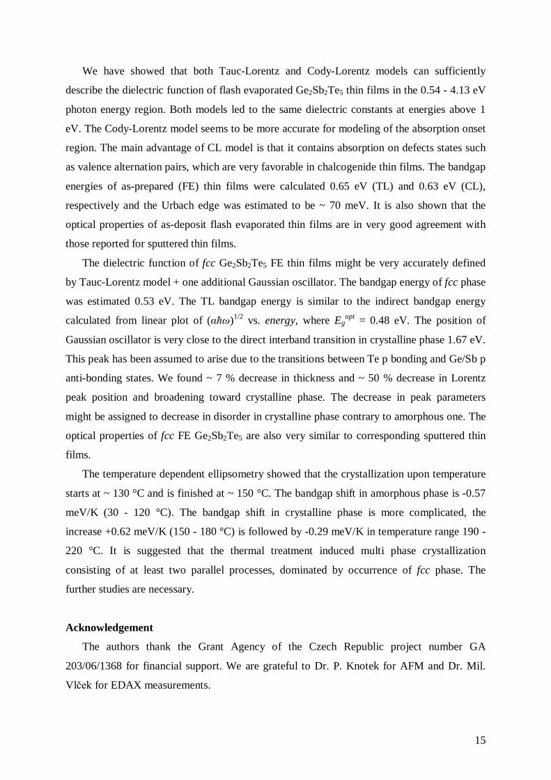
crystalline Ge2Sb2Te5 in the entire spectral region is depicted in Figs. 3a and 3b. There is a
significant decrease in the optical bandgap energy Egopt from 0.65 eV to 0.53 eV and main TL
parameters, i.e., peak broadening C (from 3.91 eV to 2.13 eV) and peak position E0 (2.55 eV
to 1.32 eV) contrary to amorphous phase (Tab. 1). On the other hand the peak amplitude
increased from 114 eV to 181 eV. This increase is also accompanied by higher values of ε2
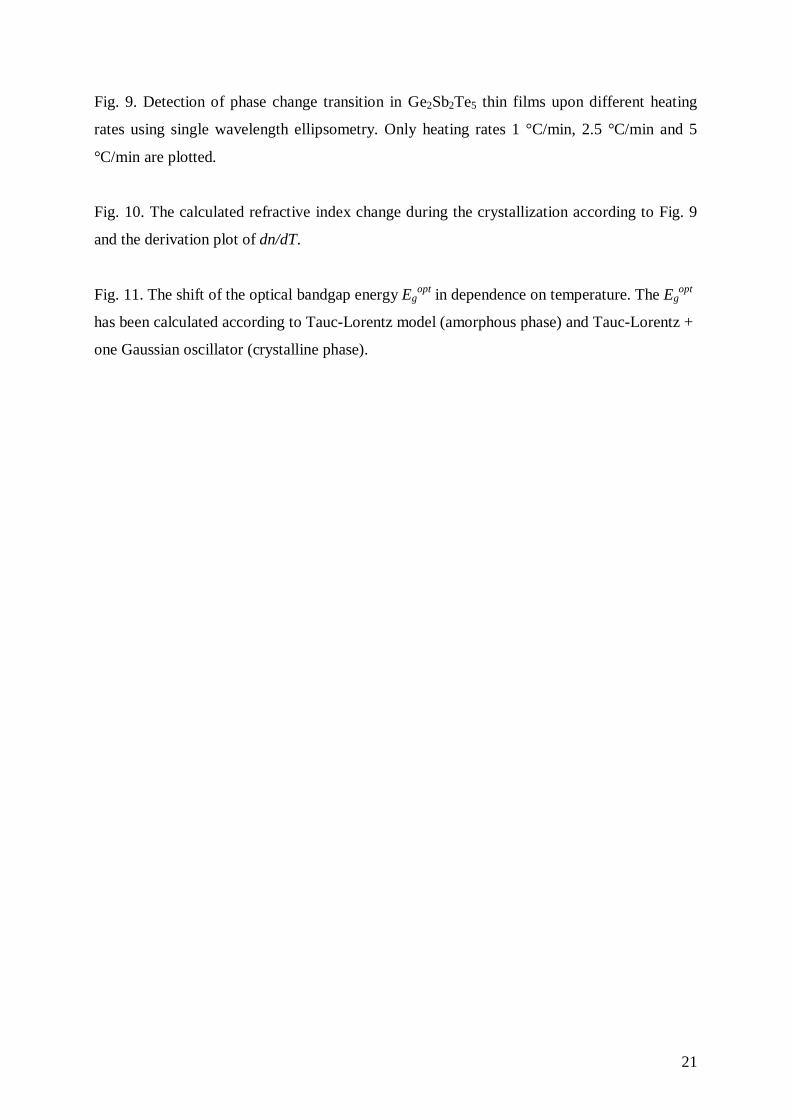
around E0 in crystalline phase contrary to amorphous one (Fig. 4b). The ε2 maximum is
determined by amplitude contributions from Lorentz oscillator, Eq. (9) and additional
Gaussian oscillator, Eq. (12). The Fig. 4 shows calculated values of ε1 and ε2 of studied
samples. The inserted figures show the behavior of refractive index n and extinction
coefficient k. The observed thickness decrease was ~ 7 % from amorphous to crystalline
(from 195 nm to 181 nm). The MSE error of fcc phase is distinctively higher without using
one additional Gaussian oscillator in the entire model MSE ~ 4. Without using the Gaussian
oscillator a significant difference between experimental and modeled data could be found at ~
1 eV photon energy and above. Adding additional oscillator at photon energy ~ 1.8 eV helps
to overcome this experimental to model data discrepancy. Kato et al. [7] showed that the
absorption spectra of fcc phase could be more satisfactory fitted by indirect absorption
formula αћω ~ (ћω - Egopt)2 than by direct, where αћω ~ (ћω - Eg
opt)1/2. The former equation
gave us Egopt = 0.48 eV, which is very close to our TL optical bandgap energy 0.53 eV. The
direct interband transition formula resulted in Egopt = 1.67 eV (Fig. 5).
The differences (errors) between experimental and modeled pseudodielectric spectra of
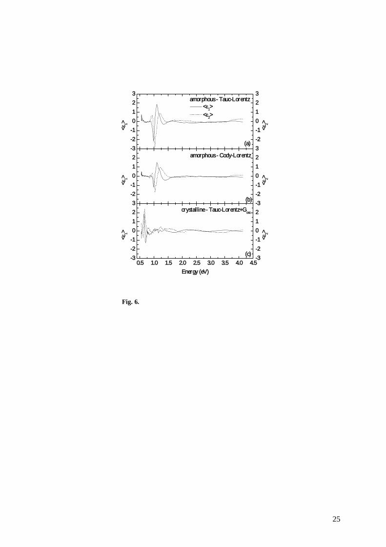
amorphous and crystalline phases are depicted in Fig. 6a (amorphous - Tauc-Lorentz model),
Fig. 6b (amorphous - Cody-Lorentz model) and Fig. 6c (crystalline - Tauc-Lorentz +
Gaussian oscillator model). The deeper look at the region around the bandgap energy of
amorphous phase TL vs. CL is depicted separately in Fig. 7 for <ε1> (Fig. 7a) and <ε2> (Fig.
7b). The difference between experimental and modeled data is slightly lower in the case of
CL model than those fitted by TL around the bandgap energy (Figs. 7a and 7b).

10
The XRD spectra of as-prepared (amorphous) and thermally crystallized (annealed at 220
°C) Ge2Sb2Te5 thin films are shown in Fig. 8. The hkl parameters of fcc phase could be
assigned according to Yamada et al. [24], where (111) 2θ = 25.59°, (200) 2θ = 29.63°, (220)
2θ = 42.40° and (222) 2θ = 52.58°. The AFM surface roughness of studied samples was found
to be lower than the optical surface roughness calculated from ellipsometry. The former
method gave us surface roughness 2.6 nm (amorphous) and 5.7 nm (fcc), respectively. The
surface roughness calculated from ellipsometry was 6 nm and for amorphous and 7.5 nm for
crystalline phase. Higher ellipsometry values may mean that EMA layer accounts for surface
roughness as well as few nanometers of oxide layer. It is supposed that GeSbTe ternary alloys
might be subject to long time oxidation, nevertheless details are not known [7].
The temperature dependent ellipsometry, i.e., behavior of Ψ and Δ upon heating is
depicted in Fig. 9 at λ = 1700 nm. The contribution of bulk oxide glassy substrate to the
change of Ψ and Δ could be considered as negligible, i.e., the change of substrate in Ψ was
detected to be ~ 0.1 deg and in Δ ~ 0.3 deg in the temperature range 30 - 300 °C. The small
change in Ψ and Δ is followed by very slight change of long wavelength refractive index at
third decimal place, which is the detection limit of the temperature dependent spectral
ellipsometry measurement. The abrupt change in Ψ and Δ in the temperature range 130 - 150
°C is due to the phase change transition (amorphous to crystalline) occurring in the Ge2Sb2Te5
thin films. The phase change transition shifts towards higher temperatures with increasing
heating rate, i.e., 1 °C/min, 2.5 °C/min and 5 °C/min. The Fig. 10 shows the temperature
dependence of refractive index on temperature as calculated from Fig. 9 (2 °C/min, λ = 1700
nm). The maximal error in determination of refractive index of Ge2Sb2Te5 thin films at the
single wavelength ellipsometry was ± 0.04. The Fig. 10 also shows temperature derivation of
dn/dT. The spectrum has been taken as single wavelength ellipsometry at λ = 1700 nm with
repeating cycle of one point ~ 6 s.
The temperature dependent spectral ellipsometry (300 - 2300 nm) was done to calculate
the absorption edge shift of amorphous and crystalline phases (Fig. 11). The absorption edge
of amorphous phase shows linear redshift with coefficient -0.57 meV/K, in the temperature
range 30 - 120 °C. The crystalline phase possesses more complex change of short-wavelength
absorption edge. In the temperature range 150 - 180 °C we obtained +0.62 meV/K and 190 -
220 °C -0.29 meV/K shift of optical bandgap energy. The Tauc-Lorentz model was used to
obtain the bandgap shift in the temperature range 30 - 120 °C. The bandgap shift in
temperature range 150 - 180 °C and 190 - 220 °C was calculated using combination of Tauc-
Lorentz with one additional Gaussian oscillator. The characteristic averages MSE for one
11
angle fits (70°) in the entire spectral region are ~ 3.9 in the case of amorphous phase and ~ 1.0
for crystalline phase.
5. Discussion
The both presented models, i.e., Tauc-Lorentz and Cody-Lorentz are able to describe the
dielectric function of flash evaporated amorphous Ge2Sb2Te5 thin films (Figs. 1 and 2). They
possess overall good agreement between experimental and modeled data in the entire spectral
region. Both models behave similarly at higher energies, i.e., ~ 1.5 eV up to 4.13 eV. This
region is governed by the same Lorentz oscillator formula L(E) in both models [Eqns. (9) and
(11b)]. Both TL and CL Lorentz function resemble in the peak broadening C and position E0
(Tab. 1). The main difference is in the amplitude A, where L(E) compensates different
magnitude of G(E) in Eqns. (9) and (11b). First distinguished difference in the ε2 spectra (Fig.
2) is seen at Egopt + Ep = 1.18 eV (Tab.1). In the CL model this region separates the behavior
of absorption onset from Lorentz oscillator behavior. This so called second transition provides
higher flexibility for absorption shape modeling of CL model contrary to TL model [16, 17
and 18]. The outstanding discrepancy in TL and CL ε2 spectra is at first transition energy Et =
0.79 eV (Fig. 2), which corresponds to demarcation energy between the Urbach tail transition
and the band-to-band transition in material according to CL model [Eq. (11a)] [18]. Below
this region (0.79 eV) the TL starts to drop sharply at ε2 = 0 resulting in bandgap energy Egopt =
0.65 eV (Tab. 1), i.e., the TL model does not describe any weak absorption tail bellow the
bandgap energy [Eq. (9)]. On the other hand CL follows Eq. (11a) in the spectral region 0 < E
≤ Et. The corresponding Egopt = 0.63 eV and Eu = 70 meV were calculated (Tab. 1) at room-
temperature. The CL matches better to the experimental data around and below the bandgap
energy as it is seen from the difference plot between <ε1> and <ε2> experimental vs. modeled
data in Figs. 6a, 6b and Figs. 7a and 7b. The found values of Egopt and Eu of amorphous phase
are in good agreement with those reported in [7]. The authors found optical bandgap energy
of DC sputtered amorphous Ge2Sb2Te5 thin films Egopt = 0.74 eV and Urbach energy ~ 50
meV from transmission spectra using Tauc plot [20], respectively. Ju et. al [25] reported
Urbach edge ~ 40 and/or ~ 90 meV in dependence on sputtering deposition rate. Value of
bandgap energy 0.7 eV (TL) and Urbach edge ~ 81 meV was reported by Lee et. al [26]. It
should be noted that the optical properties of sputtered thin films vary dramatically with
deposition conditions [5]. The bandgap energy of FE thin films is close to pulsed laser
deposited amorphous Ge2Sb2Te5 thin films, where Egopt = 0.79 eV according to PDOS model
[27]. The better fit of CL model to experimental data is also represented by lower MSE =

12
1.937 contrary to TL model MSE = 2.476. We might expect that the CL model is favorable
for amorphous Ge2Sb2Te5 thin films. The defects which are represented by non-zero
absorption below Egopt occur naturally in these materials. The defects appear as localized
states above the valence band in density of states (DOS), i.e., Urbach edge is governed by the
valence band tail [28]. It might be plausible to consider these localized states as results of
“wrong” covalently bound atoms in amorphous chalcogenides, i.e., so called valence
alternation pairs (VAPs) [29, 30 and 31]. Some studies suggested that the VAPs defects might
be created due to the over-coordinated 3-fold Te atoms as it was shown in EXAFS studies
[32, 33], since their normal valency is 2-fold. The 3-fold Te+ is then positively charged. The
negative charge is then assumed to be located at 3-fold Ge atoms and/or 2-fold Sb atoms, i.e.,
forming Ge- and/or Sb- charged centers [34, 35 and 36]. It should be noted that the problem is
still under deep study of many researchers and the VAPs model its self seems to be more
complicated in the case of telluride glasses [37] than it was proposed, e.g., for sulfide and/or
selenide glasses [31].
The Ge2Sb2Te5 crystalline phase shows more pronounced structure of dielectric function
spectra contrary to amorphous state (Fig. 4). The sharper shape has been modeled by using
Tauc-Lorentz dispersion formula with additional Gaussian oscillator (Fig. 3). It is not possible
to employ the CL model in crystalline phase. This is mainly due to the impossibility to model
the Urbach edge in highly ordered crystalline phase contrary to amorphous one. The TL
model is also favorable as it has lesser number of varying parameters. The TL model except
of its wide use in amorphous semiconductors is also very acceptable for describing optical
properties of indirect crystalline semiconductors as it was, e.g., shown for polycrystalline
bismuth selenotelluride thin films [38] and GeSbTe thin film alloys [39]. Other authors
applied multiple Lorentz oscillators [11] to describe the dielectric function of meta-stable fcc
phase [26, 40]. Older studies also applied Cauchy model [11] to describe n and k of
Ge2Sb2Te5 sputtered thin films [41]. The MSE error of TL model without using one additional
Gaussian oscillator was ~ 4. The Gaussian oscillator (MSE = 0.998) might be replaced by
classical Lorentz oscillator, i.e., MSE ~ 1.1. The Lorentz oscillator has shallower peak
behavior resulting in ineligible small absorption tail below the bandgap energy. It is of high
interest that the position of Gaussian oscillator EG = 1.77 eV (Tab. 1) is very close to the
direct transition Egopt(direct) = 1.67 eV (Fig. 5) calculated from linear region of (αE)2 vs.
energy plot. Therefore the Gaussian oscillator is assumed to be connected with direct
transition in fcc Ge2Sb2Te5 thin films. The valence band of thermally crystallized Ge2Sb2Te5
is dominated by Te, Ge and Sb p states with minor contribution from s states of Ge and Sb.

13
The conduction band is mainly populated by anti-bonding p states of Ge, Sb and p states of Te
[42]. The peak at 1.77 eV might be assigned to the transitions between Te p bonding and
Ge/Sb p anti-bonding states. Nevertheless the precise determination of the states involved in
this transition is not possible. As we mentioned in the literature data the either TL [39] or
multiple Lorentz oscillators [26, 40] are used to evaluate dielectric function of sputtered fcc
thin films. The combination of TL + Gosc or other type of oscillators as far as we know have
not been published yet for sputtered thin films. It seems to be necessary to consider further
studies of FE thin films with regard to: 1) Is the additional oscillator characteristic only for FE
fcc thermally crystallized thin films? and 2) Is the additional oscillator needed also for laser
crystallized FE thin films? Our preliminary experiments on the optically crystallized FE
Ge2Sb2Te5 thin films show significant difference in behavior of laser crystallized contrary to
thermally crystallized materials and also different approach in evaluating ellipsometry spectra
is needed. The additional oscillator seems to be also important for laser crystallized thin films
and it is plausible to take into account Lorentz oscillator rather than Gaussian oscillator. The
problem is still under study. Just to be noted that Yamanaka et. al [43] modeled
underestimated transition in hexagonal sputtered Ge2Sb2Te5 at 1.2 eV (experimental value ~
1.8 eV). This peak has been supposed to arise due to the Te p to Sb p transitions. The current
consensus supposes that the meta-stable Ge2Sb2Te5 fcc structure posses the rocksalt like
structure, which belongs into the space group Fm-3m [24]. One site (4a) of the lattice is fully
occupied by only Te atoms and the other site (4b) is randomly occupied by Ge/Sb mixing and
20 % of vacancies. [24]. The lattice parameter of ~ 6 Å has been reported for thermally
crystallized thin films [42]. Kolobov et. al proposed that Ge2Sb2Te5 does not posses rocksalt
structure but more likely consists of well-defined rigid building blocks that are randomly
oriented in space consistent with cubic symmetry [33]. The decrease in position of the Lorentz
peak E0 from 2.55 eV to 1.32 eV (amorphous to crystalline) might be caused by increase in
medium-range order (MRO) of crystalline phase [44]. This MRO change is also accompanied
by decrease in peak broadening C from ~ 3.9 eV to ~ 2.1 eV (Tab. 1). The found value of
crystalline bandgap energy 0.53 eV is in good agreement with ~ 0.5 eV reported in [7, 26 and
27]. It should be noted that the found bandgap energy of crystalline phase is at the edge of our
spectral region. Still the accurate calculation of the bandgap energy could be done with
respect to accurate model data and measuring the most part of absorption onset region (Figs.
1, 3, 7 and 8). Weidenhof et al. [45] published 6 % decrease in volume upon crystallization.
We found ~ 7 % thickness depression upon crystallization (Tab. 1). The thickness (volume)
change is expected as the amorphous phase has larger free volume than the crystalline phase.

14
The phase change transition from amorphous to crystalline state shows significant change
in the Ψ and Δ spectra (Fig. 9) and corresponding change of refractive index (Fig. 10). The
crystallization takes place between 130 - 150 °C. Just to be noted that at one measured
wavelength the corresponding refractive index and film thickness are strongly correlated. The
change of refractive index (Fig. 10) was fitted using point-by-point technique, where every
point is fitted separately regardless of any dispersion formula [Eqs. (9), (10) and (11)]. The
only fitting parameter was refractive index. The thickness was set to constant value of
amorphous phase ~ 195 nm. This fitting procedure led to lower absolute value of refractive
index of crystalline phase as the thickness was kept constant, i.e., Δn ~ 0.2 (2.8 %), at λ =
1700 nm and 200 °C. The fitting procedure does not affect the overall behavior of refractive
index as well as the abrupt change due to the crystallization. The resulting MSE of point-by-
point fit was 0.274. It has been shown that Ge2Sb2Te5 thin films may crystallize even at
temperatures ~ 110 °C [46] with grains size ~ 3 nm. This grain size is beyond our detection
limit. If we think about the 1 °C/min in first approximation as an “isothermal” measurement,
the first and second peaks might be assigned to the fast nucleation process followed by slower
grain growth during the thermal treatment [47, 48]. On the other hand the complex behavior
might be due to the coexistence of more crystallographic structures not only of the dominated
fcc phase [49] and/or phases separation could occur. More phases are also supposed to exist in
laser crystallized films, where amorphous phase around fcc grains are expected to coexist
together [24, 50]. The different lattice parameters and/or crystallization and/or separation of
different phases are favorable as the thermal treatment is slow and processes with higher
energy barrier may rise after longer time. The idea of two parallel processes might be also
supported by two significant peaks in dn/dt plot (Fig. 10). The optical bandgap of amorphous
phase shifts linearly with slope -0.57 meV/K (Fig. 11), which is in good agreement with value
found for sputtered films [7]. The bandgap shifts with +0.62 meV/K up to 180°C after the
crystallization has been finished (Figs. 9 and 10). It is of high interest that the slope has
almost the same value but inverse slope in comparison with amorphous state. The bandgap
energy shows again redshift above the 190 °C with slope -0.29 meV/K, which is in good
agreement with [7]. This might be also connected with multi phase crystallization processes
upon thermal treatment, nevertheless the more complex behavior of the bandgap energy in the
crystalline phase is not understood and needs to be studied further.
6. Conclusion
15
We have showed that both Tauc-Lorentz and Cody-Lorentz models can sufficiently
describe the dielectric function of flash evaporated Ge2Sb2Te5 thin films in the 0.54 - 4.13 eV
photon energy region. Both models led to the same dielectric constants at energies above 1
eV. The Cody-Lorentz model seems to be more accurate for modeling of the absorption onset
region. The main advantage of CL model is that it contains absorption on defects states such
as valence alternation pairs, which are very favorable in chalcogenide thin films. The bandgap
energies of as-prepared (FE) thin films were calculated 0.65 eV (TL) and 0.63 eV (CL),
respectively and the Urbach edge was estimated to be ~ 70 meV. It is also shown that the
optical properties of as-deposit flash evaporated thin films are in very good agreement with
those reported for sputtered thin films.
The dielectric function of fcc Ge2Sb2Te5 FE thin films might be very accurately defined
by Tauc-Lorentz model + one additional Gaussian oscillator. The bandgap energy of fcc phase
was estimated 0.53 eV. The TL bandgap energy is similar to the indirect bandgap energy
calculated from linear plot of (αћω)1/2 vs. energy, where Egopt = 0.48 eV. The position of
Gaussian oscillator is very close to the direct interband transition in crystalline phase 1.67 eV.
This peak has been assumed to arise due to the transitions between Te p bonding and Ge/Sb p
anti-bonding states. We found ~ 7 % decrease in thickness and ~ 50 % decrease in Lorentz
peak position and broadening toward crystalline phase. The decrease in peak parameters
might be assigned to decrease in disorder in crystalline phase contrary to amorphous one. The
optical properties of fcc FE Ge2Sb2Te5 are also very similar to corresponding sputtered thin
films.
The temperature dependent ellipsometry showed that the crystallization upon temperature
starts at ~ 130 °C and is finished at ~ 150 °C. The bandgap shift in amorphous phase is -0.57
meV/K (30 - 120 °C). The bandgap shift in crystalline phase is more complicated, the
increase +0.62 meV/K (150 - 180 °C) is followed by -0.29 meV/K in temperature range 190 -
220 °C. It is suggested that the thermal treatment induced multi phase crystallization
consisting of at least two parallel processes, dominated by occurrence of fcc phase. The
further studies are necessary.
Acknowledgement
The authors thank the Grant Agency of the Czech Republic project number GA
203/06/1368 for financial support. We are grateful to Dr. P. Knotek for AFM and Dr. Mil.
Vlček for EDAX measurements.

16

17
References 1. S. R. Ovshinsky, Application of Non-Crystalline Materials, in Insulating and
Semiconductor Glasses, edited by P. Boolchand (World Scientific Publishing Co. Pte. Ltd.,
Singapore, 2000), pp. 729-779. 2. S. R. Ovshinsky, B. Pashmakov, Mat. Res. Soc. Symp. Proc. 803, HH1.1.1. (2004). 3. M. Frumar, B. Frumarova, T. Wagner, M. Hrdlicka, J Mater Sci: Mater Electron 18, S169
(2007). 4. S. Kohara, K. Kato, S. Kimura, Hit. Tanaka, T. Usuki, K. Suzuya, Hir. Tanaka, Y.
Moritomo, T. Matsunaga, N. Yamada, Y. Tanaka, H. Suematsu, M. Takata, Appl. Phys. Lett.
89, 201910 (2006). 5. H. Dieker, M. Wuttig, Thin Solid Films 478, 248 (2005). 6. T. Ohta, S. R. Ovshinsky, Phase-Change Optical Storage Media, in Photo-Induced
Metastability in Amorphous Semiconductors, edited by A. V. Kolobov (Wiley-VCH,
Weinheim, 2003), pp. 310-326. 7. T. Kato, K. Tanaka, Jpn. J. Appl. Phys. 44, 7340 (2005). 8. R. M. A. Azzam and N. M. Bashara, Ellipsometry and Polarized Light (North-Holland,
Amsterdam, 1984). 9. H. G. Tompkins, W. A. McGahan, Spectroscopic Ellipsometry and Reflectometry (Wiley
Inter-Science, New York, 1999). 10. D. E. Aspnes, A. A. Studna, Appl. Opt. 14, 220 (1975). 11. H. G. Tompkins, E. A. Irene, Handbook of Ellipsometry (William Andrew, Inc., New
York, 2005). 12. D. E. Aspnes, A. A. Studna, Phys. Rev. B 27, 98 (1983). 13. D. E. Aspnes, J. B. Theeten, F. Hottier, Phys. Rev. B 20, 3292 (1979). 14. D. A. G. Bruggeman, Ann. Phys. 24 (1935) 636. 15. A. Mendoza-Galvan, J. Gonzalez-Hernandez, J. Appl. Phys. 87, 760 (2000). 16. G. E. Jellison, Jr., F. A. Modine, Appl. Phys. Lett. 69, 371 (1996). 17. G. E. Jellison, Jr., F. A. Modine, Appl. Phys. Lett. 69, 2137 (1996). 18. A. S. Ferlauto, G. M. Ferreira, J. M. Pearce, C. R. Wronski, R. W. Collins, X. Deng, G.
Ganguly J. Appl. Phys. 92, 2424 (2002). 19. N. F. Mott, E. A. Davis, Electronic Processes in Non-Crystalline Materials (Clarendon
Press, Oxford, 1971). 20. J. Tauc, R. Grigorovic, A. Vancu, Phys. Stat. Sol. 15, 627 (1966). 21. A. R. Forouhi, I. Bloomer, Phys. Rev. B 34, 7018 (1986).

18
22. A. R. Forouhi, I. Bloomer, Phys. Rev. B 38, 1865 (1988). 23. J. Tauc, Optical Properties of Non-Crystalline Solids, in Optical Properties of Solids,
edited by F. Abeles (North-Holland Publishing Company, Amsterdam, 1972), pp. 278-313. 24. N. Yamada, T. Mastunaga, J. Appl. Phys. 88, 7020 (2000). 25. T. Ju, J. Viner, H. Li, P. C. Taylor, J. Non-Cryst. Solids (2008),
doi:10.1016/j.jnoncrysol.2007.10.088. 26. Bong-Sub Lee, J. R. Abelson, S. G. Bishop, Dae-Hwan Kang, Byung-ki Cheong, Ki-Bum
Kim, J. Appl. Phys. 97, 093509 (2005). 27. D. Franta, M. Hrdlicka, D. Necas, M. Frumar, I. Ohlidal, M. Pavlista, Phys. Stat. Sol. (c)
1-4 (2008), doi:10.1002/pssc.200777768. 28. K. Tanaka, J. Optoelectron. Adv. Mater. 3, 189 (2001). 29. H. Fritzsche, J. Phys. Chem. Solids 68, 878 (2007). 30. M. Popescu, Structure, Defects and Electronic Properties of Amorphous Semiconductors,
in Photo-Induced Metastability in a-Semiconductors, edited by A. V. Kolobov (WILEY-
VCH, Weinheim, 2003), pp. 1-20. 31. J. Singh, K. Shimakawa, Defects, in: Advances in Amorphous Semiconductors (Taylor &
Francis, London, 2003), pp. 158-203. 32. D. A. Baker, M. A. Paesler, G. Lucovsky, P. C. Taylor, J. Non-Cryst. Solids 352, 1621
(2006). 33. A. V. Kolobov, P. Fons, A. I. Frenkel, A. L. Ankudinov, J. Tominaga, T. Uruga, Nat.
Mater. 3, 703 (2004). 34. M. A. Paesler, D. A. Baker, G. Lucovsky, A. E. Edwards, P. C. Taylor, J. Phys. Chem.
Solids 68, 873 (2007). 35. D. A. Baker, M. A. Paesler, G. Lucovsky, S. C. Agarwal, P. C. Taylor, Phys. Rev. Lett.
96, 25551 (2006). 36. G. Lucovsky, D. A. Baker, M. A. Paesler, J. C. Philips, J. Non-Cryst. Solids 353, 1713
(2007). 37. J. Robertson, K. Xiong, P. W. Peacock, Thin Solid Films 515, 7538 (2007). 38. A. Zimmer, N. Stein, H. Terryn, C. Boulanger, J. Phys. Chem. Solids 68, 1902 (2007). 39. A. Chabli, C. Vergnaud, F. Bertin, V. Gehanno, B. Valon, B. Hyot, B. Bechevet, M.
Burdin, D. Muyard, J. Magn. Magn. Mater. 249, 509 (2002). 40. E. Garcia-Garcia, A. Mendoza-Galvan, Y. Vorobiev, E. Morales-Sanchez, J. Gonzalez-
Hernandez, G. Martinez, B. S. Chao, J. Vac. Sci. Technol. A17, 1805 (1999). 41. T. Ide. M. Suzuki, M. Okada, Jpn. J. Appl. Phys. 34, L529 (1995).

19
42. Z. Sun, S. Krysta, D. Music, R. Ahuja, J. M. Schneider, Solid State Communications 143,
240 (2007). 43. S. Yamanaka, S. Ogawa, I. Morimoto, Y. Ueshima, Jpn. J. Appl. Phys. 37, 3327 (1998). 44. M. Niato, M. Ishimaru, Y. Hirotsu, M. Takashima, J. Non-Cryst. Solids 354&346, 112
(2004). 45. V. Weidenhof, I. Friedrich, S. Ziegler, M. Wuttig, J. Appl. Phys. 86, 5879 (1999). 46. Yu Jin Park, Jeong Yong Lee, Yong Tae Kim, Appl. Surf. Sci. 252, 8102 (2006). 47. Dohyung Kim, Sang Jun Kim, Sung-Hyuck An, Sang Youl Kim, Jpn. J. Appl. Phys. 42
5107 (2003). 48. Sung-Hyuck An, Dohyung Kim, Sang Youl Kim, Jpn. J. Appl. Phys. 41, 7400 (2002). 49. B. J. Kooi, W. M. G. Groot, J. Th. M. De Hosson, J. Appl. Phys. 95, 924 (2004). 50. G. Lucovsky, J. C. Phillips, J. Non-Cryst. Solids (2008),
doi:10.1010/j.jnoncrysol.2007.09.059.

20
Figure captions
Fig. 1. Real <ε1> (a) and imaginary <ε2> (b) parts of the pseudodielectric function <ε> for
amorphous Ge2Sb2Te5 thin films calculated according to Tauc-Lorentz and Cody-Lorentz
models (circles: experimental data, solid lines: best-fit calculation). The inserted figures show
model and experimental data agreement in the absorption onset region.
Fig. 2. Comparison of ε2 of amorphous Ge2Sb2Te5 thin film calculated according to Tauc-
Lorentz and Cody-Lorentz models. The inserted figure shows the behavior of ε2 in the
absorption onset.
Fig. 3. Real <ε1> (a) and imaginary <ε2> (b) parts of the pseudodielectric function <ε> for
crystalline Ge2Sb2Te5 thin films calculated according to Tauc-Lorentz + Gaussian oscillator
(circles: experimental data, solid lines: best-fit calculation).
Fig. 4. The calculated real ε1 (a) and imaginary ε2 (b) part of dielectric function of amorphous
and crystalline Ge2Sb2Te5 thin films. The inserted pictures show the corresponding refractive
index and extinction coefficient.
Fig. 5. Tauc plots: (αE)1/2 - Egopt = 0.48 eV and (αE)2 - Eg
opt = 1.67 eV as function of photon
energy E (~ 195 nm, crystallized Ge2Sb2Te5).
Fig. 6. Difference between experimental and modeled data of (a) amorphous - Tauc-Lorentz,
(b) amorphous - Cody-Lorentz and (c) crystalline - Tauc-Lorentz + Gaussian oscillator
Ge2Sb2Te5 thin films.
Fig. 7. Difference between experimental and modeled data of amorphous Ge2Sb2Te5
calculated according to Tauc-Lorentz and Cody-Lorentz models in the absorption onset
region. (a) Δ<ε1>, (b) Δ<ε2>.
Fig. 8. XRD spectra of as-prepared (amorphous) and thermally crystallized Ge2Sb2Te5 thin
films. The hkl parameters of crystalline phase are assigned according to Ref. 24.
21
Fig. 9. Detection of phase change transition in Ge2Sb2Te5 thin films upon different heating
rates using single wavelength ellipsometry. Only heating rates 1 °C/min, 2.5 °C/min and 5
°C/min are plotted.
Fig. 10. The calculated refractive index change during the crystallization according to Fig. 9
and the derivation plot of dn/dT.
Fig. 11. The shift of the optical bandgap energy Egopt in dependence on temperature. The Eg
opt
has been calculated according to Tauc-Lorentz model (amorphous phase) and Tauc-Lorentz +
one Gaussian oscillator (crystalline phase).

22
0
10
20
30
40
0.52 0.54 0.56 0.58 0.60 0.62 0.64 0.66
10
20
30
<ε2>
Energy (eV)
0.52 0.54 0.56 0.58 0.60 0.62 0.64 0.66
2
4
6
8
10
<ε1>
Energy (eV)
experimental points Tauc-Lorentz Cody-Lorentz
<ε1>
amorphous Ge2Sb2Te5
(a)
0.5 1.0 1.5 2.0 2.5 3.0 3.5 4.0 4.5-30
-20
-10
0
10
20
30
<ε2>
Energy (eV)
(b)
Fig. 1.
0.0 0.5 1.0 1.5 2.0 2.5 3.0 3.5 4.0 4.51E-3
0.01
0.1
1
10
0.4 0.6 0.8 1.00.0
0.2
0.4
0.6
0.8
1.0
ε 2
Energy (eV)
CL TL
Et = 0.79 eV
Eoptg
ε 2
Energy (eV)
CL
TL
Et = 0.79 eV
Egopt + Ep = 1.18 eV
Eoptg
amorphous Ge2Sb2Te5
Fig. 2.
23
0
50
100
<ε1>
experimental data TL + Gosc model
Ge2Sb2Te5 (fcc)
(a)
0.5 1.0 1.5 2.0 2.5 3.0 3.5 4.0 4.5
-50
0
50
<ε2>
Energy (eV)
(b)
Fig. 3.
24
0
30
60
0.5 1.0 1.5 2.0 2.5 3.0 3.5 4.0 4.50
2
4
6
8
Refr
activ
e ind
ex
Energy (eV)
Tauc-Lorentz Cody-Lorentz Tauc-Lorentz + Gosc
ε 1
Ge2Sb2Te5
(a)
amorphous
fcc
0.5 1.0 1.5 2.0 2.5 3.0 3.5 4.0 4.50
20
40
0.5 1.0 1.5 2.0 2.5 3.0 3.5 4.0 4.50
1
2
3
4
5
Extin
ctio
n co
effic
ient
Energy (eV)ε 2
Energy (eV)
(b)
fcc
amorphous
0.5 1.0 1.5 2.0 2.5 3.0 3.5 4.0 4.50
500
1000
1500
2000
2500
indirect transition
(αE)
1/2 (c
m-1
/2eV
1/2 )
Energy (eV)
0.00E+000
1.00E+013
2.00E+013
3.00E+013
direct transition extrapolation
(αE)
2 (cm
-2eV
2 )
R2 = 0.9996
R2 = 0.99812
Fig. 4.
Fig. 5.
25
-3-2-10123
<ε1>
<ε1>
amorphous - Tauc-Lorentz
(a)-2-10123
<ε2>
<ε2>
-2-1012
<ε1>
amorphous - Cody-Lorentz
(b) -3-2-10123
<ε2>
0.5 1.0 1.5 2.0 2.5 3.0 3.5 4.0 4.5-3-2-10123
Energy (eV)
<ε1>
crystalline - Tauc-Lorentz+Gosc
(c)-3-2-1012
<ε2>
Fig. 6.

26
0.0
0.2
0.4
0.6
0.8
1.0
Tauc-Lorentz model Cody-Lorentz model
<ε1>
Ge2Sb2Te5
amorphous(a)
0.50 0.55 0.60 0.65 0.70 0.75 0.80-0.2
0.0
0.2
0.4
0.6
0.8
1.0
Energy (eV)
<ε2>
(b)
Fig. 7.

27
10 20 30 40 50 60 70
XRD
inte
nsity
(a.u
.)
2 Θ (deg)
as-prepared
crystalline
Ge2Sb2Te5
111
200
220
222
40 60 80 100 120 140 160 180 2004
8
12
16
20
24
28
32
Ψ (d
eg)
Temperature (°C)
-50
0
50
100
150
200
250
amorphous
crystalline
Ge2Sb2Te5
λ = 1700 nm 5 °C/min 2.5 °C/min 1 °C/min
∆ (d
eg)
amorphous
crystalline
Fig. 8.
Fig. 9.

28
40 60 80 100 120 140 160 180 2000
1
2
3
n-n 30
°C
Temperature (°C)
0.0
0.1
0.2
0.3
d(n-
n 30°C
)/dT
(1/°C
)
Ge2Sb2Te5
λ = 1700 nm2 °C/min
20 40 60 80 100 120 160 180 200 220
0.48
0.50
0.58
0.60
0.62
0.64
0.66
Eopt
g(e
V)
Temperature (°C)
300 320 340 360 380 420 440 460 480 500Temperature (K)
Ge2Sb2Te5
amorphous
crystalline
Fig. 10.
Fig. 11.
29
Tables
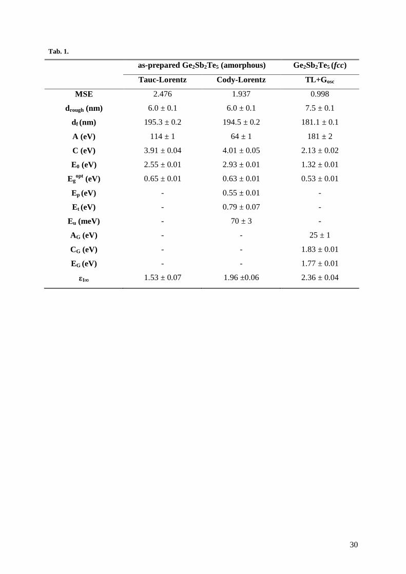
Tab. 1. Tauc-Lorentz, Cody-Lorentz and Gaussian models parameters of the studied
amorphous and crystallized Ge2Sb2Te5 FE thin films. A (AG), C (CG), E0 (EG), Egopt represent
oscillator parameters: amplitude, peak transition energy, broadening and optical bandgap
energy. Eu - Urbach energy, Et and Ep first and second transitions in CL model. ε1(∞) is a
constant contribution to the real part of dielectric function at higher energies.
30
Tab. 1.
as-prepared Ge2Sb2Te5 (amorphous) Ge2Sb2Te5 (fcc)
Tauc-Lorentz Cody-Lorentz TL+Gosc
MSE 2.476 1.937 0.998
drough (nm) 6.0 ± 0.1 6.0 ± 0.1 7.5 ± 0.1
df (nm) 195.3 ± 0.2 194.5 ± 0.2 181.1 ± 0.1
A (eV) 114 ± 1 64 ± 1 181 ± 2
C (eV) 3.91 ± 0.04 4.01 ± 0.05 2.13 ± 0.02
E0 (eV) 2.55 ± 0.01 2.93 ± 0.01 1.32 ± 0.01
Egopt (eV) 0.65 ± 0.01 0.63 ± 0.01 0.53 ± 0.01
Ep (eV) - 0.55 ± 0.01 -
Et (eV) - 0.79 ± 0.07 -
Eu (meV) - 70 ± 3 -
AG (eV) - - 25 ± 1
CG (eV) - - 1.83 ± 0.01
EG (eV) - - 1.77 ± 0.01
ε1∞ 1.53 ± 0.07 1.96 ±0.06 2.36 ± 0.04
Related Documents


