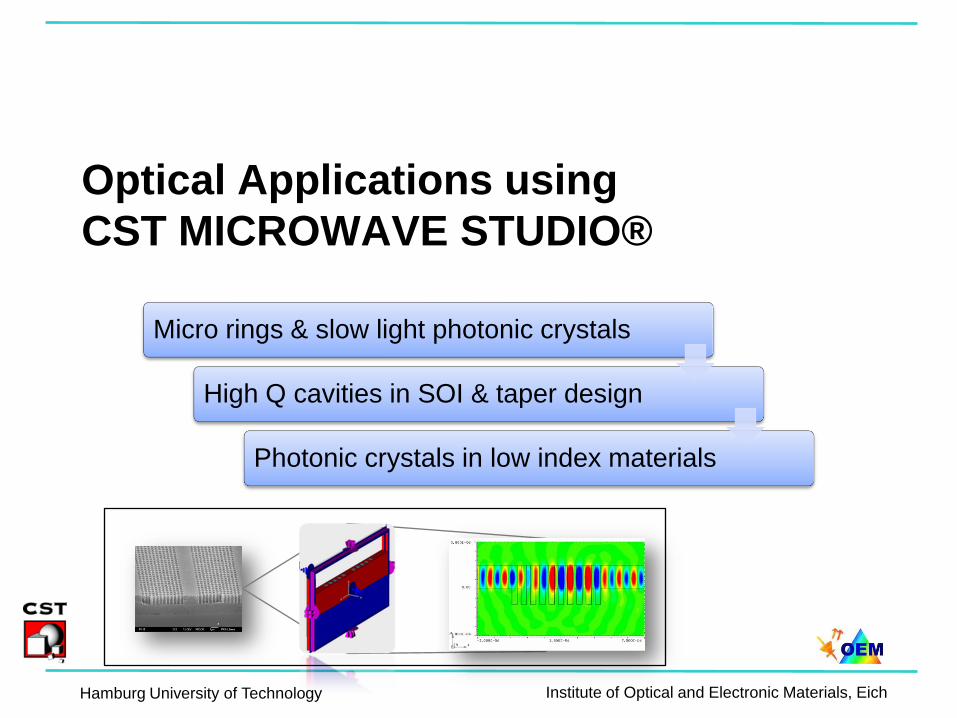
Hamburg University of Technology Institute of Optical and Electronic Materials, Eich Optical Applications using CST MICROWAVE STUDIO® Micro rings & slow light photonic crystals High Q cavities in SOI & taper design Photonic crystals in low index materials

Welcome message from author
This document is posted to help you gain knowledge. Please leave a comment to let me know what you think about it! Share it to your friends and learn new things together.
Transcript
Hamburg University of Technology Institute of Optical and Electronic Materials, Eich
Optical Applications using
CST MICROWAVE STUDIO®
Micro rings & slow light photonic crystals
High Q cavities in SOI & taper design
Photonic crystals in low index materials

Hamburg University of Technology Institute of Optical and Electronic Materials, Eich
Optical Applications using
CST MICROWAVE STUDIO®
Micro rings & slow light photonic crystals
High Q cavities in SOI & taper design
Photonic crystals in low index materials
Hamburg University of Technology Institute of Optical and Electronic Materials, Eich
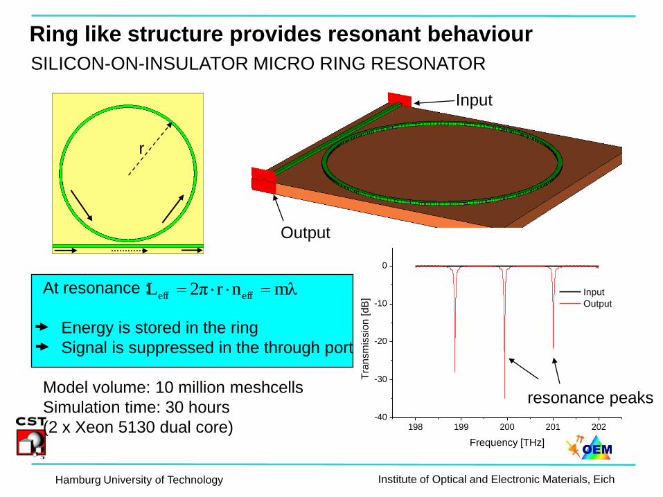
Ring like structure provides resonant behaviour
SILICON-ON-INSULATOR MICRO RING RESONATOR
Input
Output
resonance peaks
At resonance :
Energy is stored in the ring
Signal is suppressed in the through port
Model volume: 10 million meshcells
Simulation time: 30 hours
(2 x Xeon 5130 dual core)
mλnr2π L effeff
r
198 199 200 201 202-40
-30
-20
-10
0
Input
Output
Tra
nsm
issio
n [
dB
]
Frequency [THz]
Hamburg University of Technology Institute of Optical and Electronic Materials, Eich
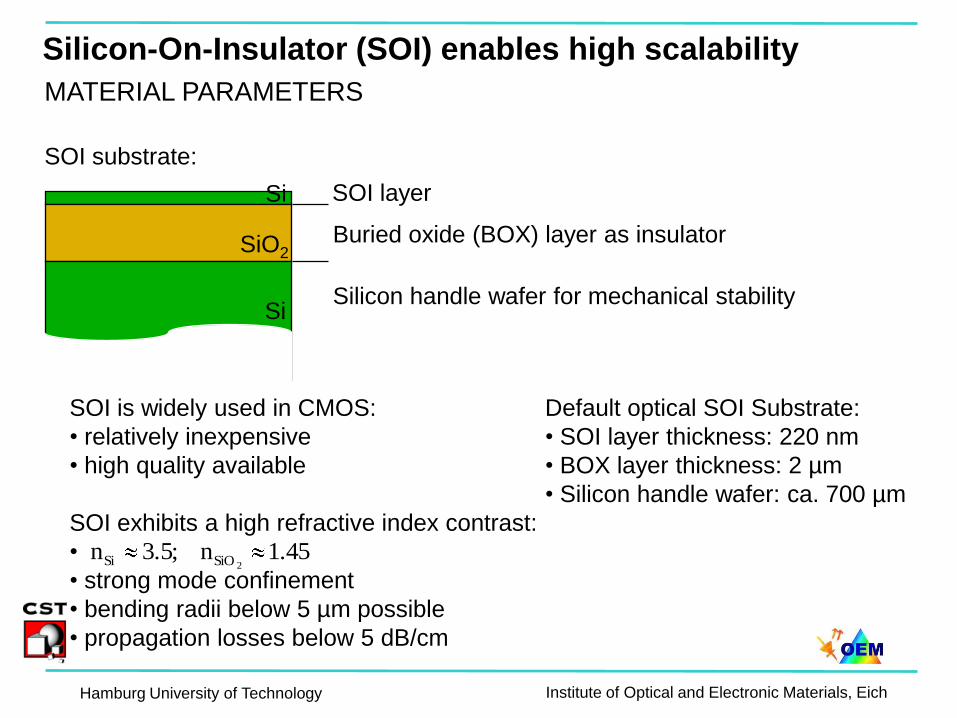
Silicon-On-Insulator (SOI) enables high scalability
MATERIAL PARAMETERS
SOI layer
Buried oxide (BOX) layer as insulator
Silicon handle wafer for mechanical stability
SiO2
Si
Si
SOI substrate:
SOI is widely used in CMOS:
• relatively inexpensive
• high quality available
SOI exhibits a high refractive index contrast:
•
• strong mode confinement
• bending radii below 5 µm possible
• propagation losses below 5 dB/cm
1.45n;3.5n2SiOSi
Default optical SOI Substrate:
• SOI layer thickness: 220 nm
• BOX layer thickness: 2 µm
• Silicon handle wafer: ca. 700 µm
Hamburg University of Technology Institute of Optical and Electronic Materials, Eich
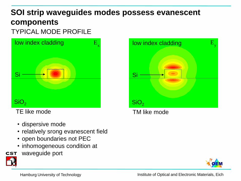
SOI strip waveguides modes possess evanescent
componentsTYPICAL MODE PROFILE
TE like mode TM like mode
• dispersive mode
• relatively srong evanescent field
• open boundaries not PEC
• inhomogeneous condition at
waveguide port
SiO2
low index cladding
Si
SiO2
low index cladding
Si
xE
yE

Hamburg University of Technology Institute of Optical and Electronic Materials, Eich
Race track shape allows more efficient design of coupling
RACE TRACK MODEL EXAMPLE
Lc
r
dcgap
Radius r has influence on:
• effective coupling length Lc
• losses due to both bending and
coupling
Introducing straight part of length
Lc helps tailoring the coupling
condition
r = 10 µm
gap = 400 nm
Lc = 1 – 10 µm

Hamburg University of Technology Institute of Optical and Electronic Materials, Eich
Nanophotonic models may need non standard CST MWS
building blocksMODEL EVOLUTION
• 90° curve model
• 10 µm radius
• default number of
segments
• partly trimed cylinder
More than 3 million meshcells and
more than 1 hour simulation time on a Pentium 4 (3 GHz) CPU
Input
Output
• 1500 segments per
360° turn
• E-field pattern is as
expected

Hamburg University of Technology Institute of Optical and Electronic Materials, Eich
Investigation of coupling demands large models
MODEL FOR DIRECTIONAL COUPLING
50 µm
• almost 30 million meshcells
• 16 hours simulation time
• distributed computing on a 2 x dual core XEON 5130 (8 GB RAM)
Model design:
• 90° bend necessary for absorption reasons (third port)
• field monitors needed
Hamburg University of Technology Institute of Optical and Electronic Materials, Eich
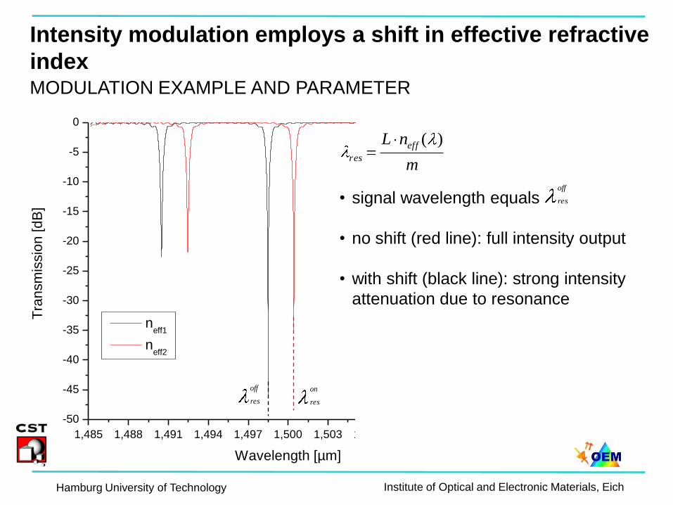
Intensity modulation employs a shift in effective refractive
indexMODULATION EXAMPLE AND PARAMETER
m
nL eff
res
)(
on
res
off
res
• signal wavelength equals
• no shift (red line): full intensity output
• with shift (black line): strong intensity
attenuation due to resonance
off
res
1,485 1,488 1,491 1,494 1,497 1,500 1,503 1,506 1,509 1,512 1,515
-50
-45
-40
-35
-30
-25
-20
-15
-10
-5
0
Tra
nsm
issio
n [d
B]
Wavelength [µm]
neff1
neff2

Hamburg University of Technology Institute of Optical and Electronic Materials, Eich
Two different conditions have been considered
MODELS FOR OPTIMIZING
SiO2
polymer
SiO2
polymer
active zone
silicon strip waveguide
silicon slot waveguide
• quasi TE mode
• both silicon rails act as electrode
• strong evanescent field
enhancement in slot
• quasi TM mode
• silicon strip acts as lower electrode
• upper electrode on top of polymer
optE
optE
External n is transferred
to neff via evanescent field

Hamburg University of Technology Institute of Optical and Electronic Materials, Eich
CST MWS “2D Port Mode Calculation” has been used
MODEL FOR 2D CALCULATION
SiO2
Polymer
Si
active zone
model
length
• models are very short (500 nm)
• length limitation due to port definition
• parameter sweep over geometry and
dielectric constant in actice zone
• user defined result watch (e.g. beta)

Hamburg University of Technology Institute of Optical and Electronic Materials, Eich
CST MWS 3D Eigenmode Solver is used for photonic
band calculationsMODELS FOR BANDDIAGRAM CALCULATION
3D Eigenmode solver:
• single unit cell models
• parameter sweep over phase shift
(defines k) at periodic boundary
• user defined result watch
• quasi 2D model is one mesh cell
in height
quasi 2D model
3D model

Hamburg University of Technology Institute of Optical and Electronic Materials, Eich
Certain photonic crystal (PhC) line defects exhibit “slow
light” regionBANDDIAGRAM AND FIELD DISTRIBUTION
dK
Kdvg
)(
a30,7W0.7a3W1
XZ
a
a aH
Hamburg University of Technology Institute of Optical and Electronic Materials, Eich
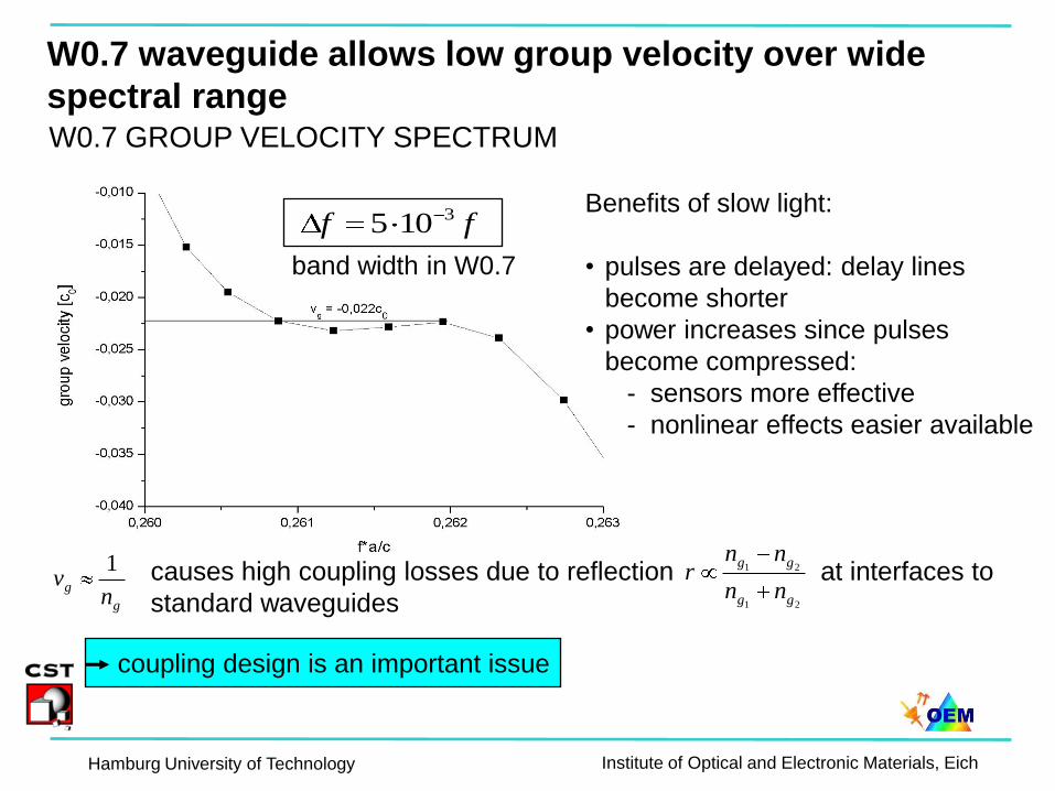
W0.7 waveguide allows low group velocity over wide
spectral rangeW0.7 GROUP VELOCITY SPECTRUM
ff 3105
band width in W0.7
g
gn
v1
21
21
gg
gg
nn
nnr
Benefits of slow light:
• pulses are delayed: delay lines
become shorter
• power increases since pulses
become compressed:
- sensors more effective
- nonlinear effects easier available
causes high coupling losses due to reflection at interfaces to
standard waveguides
coupling design is an important issue

Hamburg University of Technology Institute of Optical and Electronic Materials, Eich
Index distribution at the end of PhC influences coupling
W0.7
0
1
W0.7
CUTTING FACTOR AND SURFACE MODE
X
Z
2,07,0
X
Z
H-field
distribution of a
surface mode
at
• defines position of the cut through PhC lattice constant at
the strip to PhC defect waveguide interface
• different cuts lead to different refractive index distributions
along the interface (x)
• confined modes (evanescent in z) also along the interface
in x direction
and

Hamburg University of Technology Institute of Optical and Electronic Materials, Eich
XZ
Y
Quasi 2D models under investigation have symmetric
conditions at the input and output port
MODEL FOR COUPLING OPTIMIZATION
large models for transient simulations:
• to ensure settled mode transformation
• symmetric conditions for the ports
• reasonable TE mode is selected via magnetic boundaries in y direction and
electric field symmetry along z

Hamburg University of Technology Institute of Optical and Electronic Materials, Eich
Optical Applications using
CST MICROWAVE STUDIO®
Micro rings & slow light photonic crystals
High Q cavities in SOI & taper design
Photonic crystals in low index materials
Hamburg University of Technology Institute of Optical and Electronic Materials, Eich
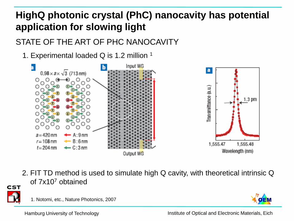
HighQ photonic crystal (PhC) nanocavity has potential
application for slowing light
STATE OF THE ART OF PHC NANOCAVITY
1. Experimental loaded Q is 1.2 million 1
2. FIT TD method is used to simulate high Q cavity, with theoretical intrinsic Q
of 7x10⁷ obtained
1. Notomi, etc., Nature Photonics, 2007
Hamburg University of Technology Institute of Optical and Electronic Materials, Eich
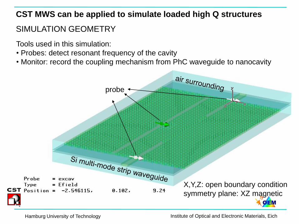
CST MWS can be applied to simulate loaded high Q structures
SIMULATION GEOMETRY
probe
Tools used in this simulation:
• Probes: detect resonant frequency of the cavity
• Monitor: record the coupling mechanism from PhC waveguide to nanocavity
X,Y,Z: open boundary condition
symmetry plane: XZ magnetic
Hamburg University of Technology Institute of Optical and Electronic Materials, Eich
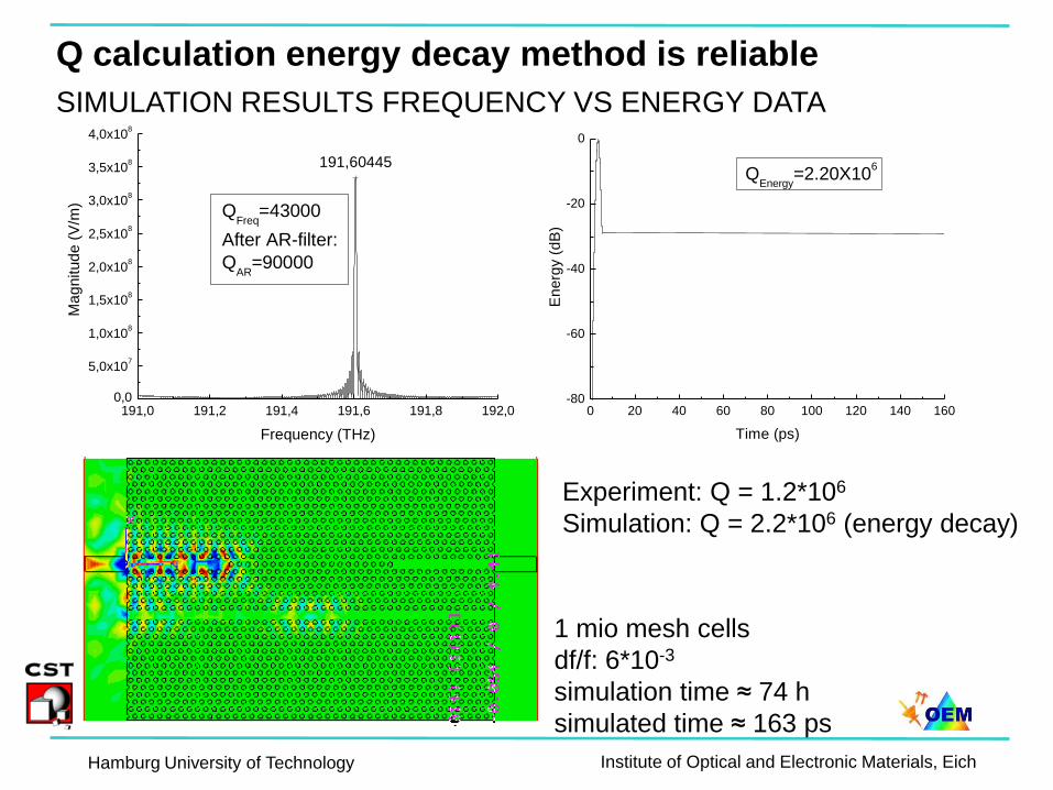
Q calculation energy decay method is reliable
SIMULATION RESULTS FREQUENCY VS ENERGY DATA
Experiment: Q = 1.2*106
Simulation: Q = 2.2*106 (energy decay)
1 mio mesh cells
df/f: 6*10-3
simulation time ≈ 74 h
simulated time ≈ 163 ps
191,0 191,2 191,4 191,6 191,8 192,00,0
5,0x10⁷
1,0x10⁸
1,5x10⁸
2,0x10⁸
2,5x10⁸
3,0x10⁸
3,5x10⁸
4,0x10⁸
191,60445
Ma
gnitud
e (
V/m
)
Frequency (THz)
QFreq
=43000
After AR-filter:
QAR
=90000
0 20 40 60 80 100 120 140 160-80
-60
-40
-20
0
En
erg
y (
dB
)
Time (ps)
QEnergy
=2.20X10⁶

Hamburg University of Technology Institute of Optical and Electronic Materials, Eich
Here is amplitude decay rate, where E(t)=E0*exp(-t/ )
Energy decay per unit (here ps) t1-t2=1ps:
Q factor can be easily calculated from energy decay rateDERIVATION OF Q FROM ENERGY DECAY
)/2exp()/2exp(
)/2exp(
)(
)(
20
10
2
1
tW
tW
tW
tW
)10ln(
)/2(10)]/2lg[exp(10
ps
dB
dt
dW
10
)10ln(/2
ps
dB
dt
dW
][)10ln(
100
psdB
dtdW
Q
dtdW
WQ 0
/2
/
0
0
dtQ
WdW
)/2exp(0 tWW
dtWdW )/2(
0 2 4 6 8 10 12-80
-60
-40
-20
0
Ene
rgy (
dB
)
Time (ps)

Hamburg University of Technology Institute of Optical and Electronic Materials, Eich
Simulation results of low Q PhC nanocavity using CST
MWS are reasonableSIMULATION RESULTS COMPARED WITH EXPERIMENT
7 layers
outs
ide t
he c
avity
Experimental loaded Q ≈ 2600 @ λ≈1567nm
Simulated intrinsic Q ≈ 4100 @ λ= 1563.4nm
x
z
X,Y,Z: open boundary condition
symmetry plane:
• XZ magnetic
• YZ electric
• XY magnetic
0 2 4 6 8 10 12
-100
-80
-60
-40
-20
0
Energ
y (
dB
)
Time (ps)
H7A00 n=3.4
Simulation: Q=4100
Experiment: Q=2600

Hamburg University of Technology Institute of Optical and Electronic Materials, Eich
f=152.706THz
Q=2.84x10⁸
f=152.715THz
Q=9.79x10⁶
Quasi 2D simulation can be used to find out optimal
coupling from PhC waveguide to nanocavity
EXAMPLES AND RESULTS
70 000 mesh cells
4h
Boundary condition:
X, Z: open
Y: magnetic
x
z
152,2 152,4 152,6 152,8 153,0 153,2 153,40,0
2,0x10⁷
4,0x10⁷
6,0x10⁷
8,0x10⁷
3,7x10⁸
3,8x10⁸
3,8x10⁸
Am
plit
ud
e
Frequency (THz)
s0 probe @ inside cavity
s0 probe @ output
s5 probe @ inside cavity
s5 probe @ output

Hamburg University of Technology Institute of Optical and Electronic Materials, Eich
Polymer cladded inverse taper structure optimizes fiber
to chip couplingSIMULATION STRUCTURE
Si taper tip
8million mesh cells
df 30THz
18h (to 4.7ps)polymer
waveguide
air
z x
y
X,Y,Z: open boundary condition
symmetry plane: YZ electricSi taper end

Hamburg University of Technology Institute of Optical and Electronic Materials, Eich
Polymer waveguide covering taper is used to increase
the tolerance of cleavingSIMULATION RESULTS
1,8x10¹⁴
1,9x10¹⁴
1,9x10¹⁴
2,0x10¹⁴
2,0x10¹⁴
2,0x10¹⁴
2,1x10¹⁴
-1,4
-1,3
-1,2
-1,1
-1,0
-0,9
-0,8
-0,7
-0,6
-0,5
Frequency (Hz)
Tra
nsm
issio
n (
dB
)
dis 10µm
dis 30µm
1,8x10¹⁴
1,9x10¹⁴
1,9x10¹⁴
2,0x10¹⁴
2,0x10¹⁴
2,0x10¹⁴
2,1x10¹⁴
-60
-50
-40
-30
-20
-10
Reflectio
n (
dB
)
Frequency (Hz)
dis 10µm
dis 30µm

Hamburg University of Technology Institute of Optical and Electronic Materials, Eich
Transmission properties are stable above 2 µm taper
length
TRANSMISSION AND REFLECTION
taper length
silicaair
X,Y,Z: open boundary condition
symmetry plane: YZ electric2µm: 58000 mesh cells, (10 min)
50µm: 520000 mesh cells, (5 h)
z x
y
1,8x10¹⁴
1,9x10¹⁴
1,9x10¹⁴
2,0x10¹⁴
2,0x10¹⁴
2,0x10¹⁴
2,1x10¹⁴
-0,68
-0,66
-0,64
-0,62
-0,60
-0,58
-0,56
-0,54
-0,52
Tra
nsm
issio
n th
rou
gh
po
rt 2
(d
B)
Frequency (Hz)
2 m
8 m
50 m
Hamburg University of Technology Institute of Optical and Electronic Materials, Eich
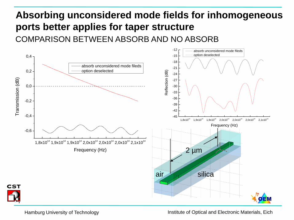
Absorbing unconsidered mode fields for inhomogeneous
ports better applies for taper structure
COMPARISON BETWEEN ABSORB AND NO ABSORB
2 µm
silicaair
1,8x10¹⁴
1,9x10¹⁴
1,9x10¹⁴
2,0x10¹⁴
2,0x10¹⁴
2,0x10¹⁴
2,1x10¹⁴
-0,6
-0,4
-0,2
0,0
0,2
0,4
absorb unconsidered mode fileds
option deselected
Tra
nsm
issio
n (
dB
)
Frequency (Hz)
1,8x10¹⁴
1,9x10¹⁴
1,9x10¹⁴
2,0x10¹⁴
2,0x10¹⁴
2,0x10¹⁴
2,1x10¹⁴
-45
-42
-39
-36
-33
-30
-27
-24
-21
-18
-15
-12
Reflection (
dB
)
Frequency (Hz)
absorb unconsidered mode fileds
option deselected

Hamburg University of Technology Institute of Optical and Electronic Materials, Eich
No absorbing unconsidered mode fields for
inhomogeneous ports better applies for PhC structureCOMPARISON BETWEEN ABSORB AND NO ABSORB
0 20 40 60 80 100 120 140 160-160
-140
-120
-100
-80
-60
-40
-20
0
En
erg
y (
dB
)
Time (ps)
3d simulation of Notomi's model
option deselected
absorb unconsidered mode fields
191,0 191,2 191,4 191,6 191,8 192,0
0,0
5,0x10⁷
1,0x10⁸
1,5x10⁸
2,0x10⁸
2,5x10⁸
3,0x10⁸
3,5x10⁸
4,0x10⁸
191,60445
3d simulation of Notomi's model
option deselected
absorb unconsidered mode fields
Ma
gn
itu
de
(V
/m)
Frequency (THz)
Hamburg University of Technology Institute of Optical and Electronic Materials, Eich
Optical Applications using
CST MICROWAVE STUDIO®
Micro rings & slow light photonic crystals
High Q cavities in SOI & taper design
Photonic crystals in low index materials

Hamburg University of Technology Institute of Optical and Electronic Materials, Eich
Frequency data is used to calculate Q factor of
photonic crystal resonators in a low-n system
30.000 meshcells
Results of interest:
• Transmission spectrum
• Q and Tmax from frequency data
MODEL AND SPECTRUM OF LINE DEFECT RESONATOR

Hamburg University of Technology Institute of Optical and Electronic Materials, Eich
Field monitors are important to understand
mechanisms of the transmission spectrum
PC WAVEGUIDE TRANSMISSION FOR VARYING ETCHING DEPTHS
monochromatic at 1200nm
detch = 1.3µm
detch = 2.5µm
1000 1200 1400 1600 1800 20000,0
0,2
0,4
0,6
0,8
1,0 monochromatic 2D-BB, neff=1.50
3D-BB, etched:
2.5 µm
1.7 µm
1.5 µm
1.3 µm
Tra
nsm
issio
n
[nm]
Böttger, Eich et al., Appl. Phys. Lett. 81, 2517 (2002)

Hamburg University of Technology Institute of Optical and Electronic Materials, Eich
A shift of the hole position can be used to improve the
resonators performance
a1*a
a2*a
a3*a a3*a
a2*a
a1*a
MODEL AND DEFINITION OF PARAMETERS TO BE OPTIMIZED
To find optimal values for a1, a2 and a3
parameter sweep and optimizer were used
Hamburg University of Technology Institute of Optical and Electronic Materials, Eich
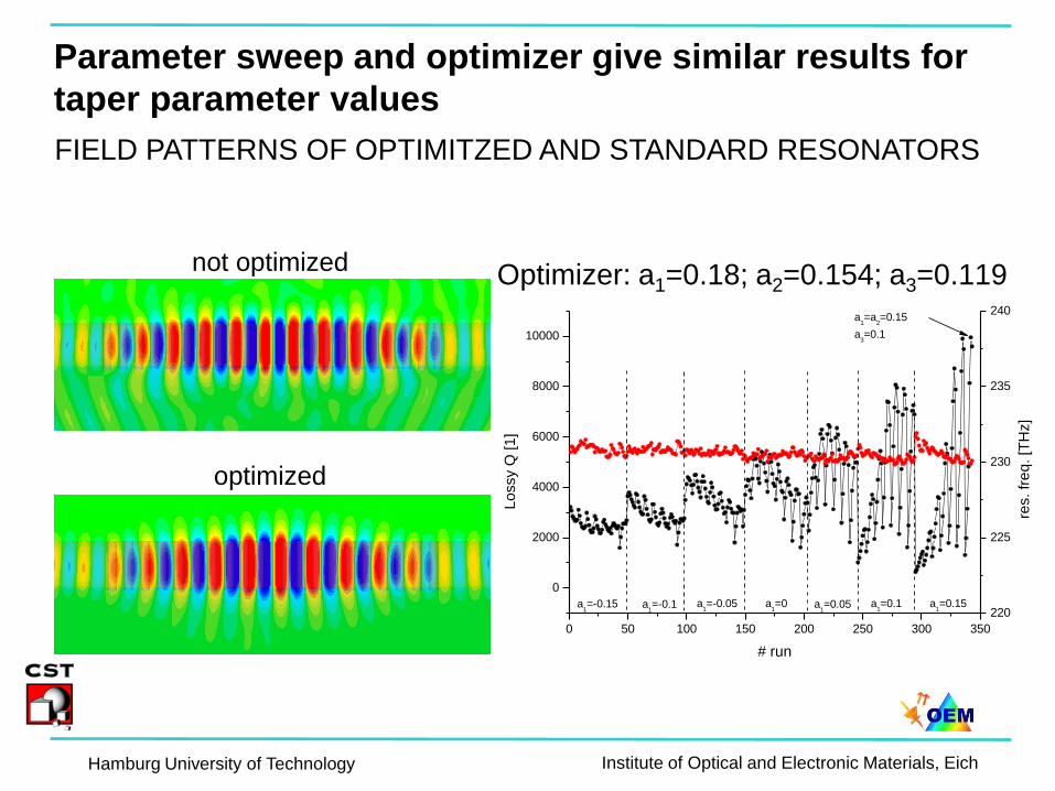
Parameter sweep and optimizer give similar results for
taper parameter values
Optimizer: a1=0.18; a2=0.154; a3=0.119
0 50 100 150 200 250 300 350
0
2000
4000
6000
8000
10000
220
225
230
235
240
a1=0.15a
1=0.1a
1=0.05a
1=0a
1=-0.05a
1=-0.1
Lo
ssy Q
[1
]
# run
a1=-0.15
a1=a
2=0.15
a3=0.1
re
s. fr
eq
. [T
Hz]
not optimized
optimized
FIELD PATTERNS OF OPTIMITZED AND STANDARD RESONATORS

Hamburg University of Technology Institute of Optical and Electronic Materials, Eich
Tapering of lattice parameters around the defect
improves resonator performance
3D SIMULATIONS OF REGULAR AND LATTICE ENGINEERED PC
aCa a
r=80nm...150nm
Three holes taper section
100 1000 10000
0,0
0,1
0,2
0,3
0,4
0,5
0,6
0,7
0,8
0,9
1,0
Tm
ax [a
.u.]
Q [1]
untapered
radius taper
lattice taper
a1 a2 a3aC a1=472nm
a2=468nm
a3=427nm

Hamburg University of Technology Institute of Optical and Electronic Materials, Eich
Ridge waveguide defect resonators require larger
simulation volume
200.000 meshcells
RIDGE WAVEGUIDE DEFECT RESONATOR STRUCTURES
• Transmission spectrum
• Q from frequency data
• High Q and model volume require
long simulation time
• Geometry optimization very time
consuming

Hamburg University of Technology Institute of Optical and Electronic Materials, Eich
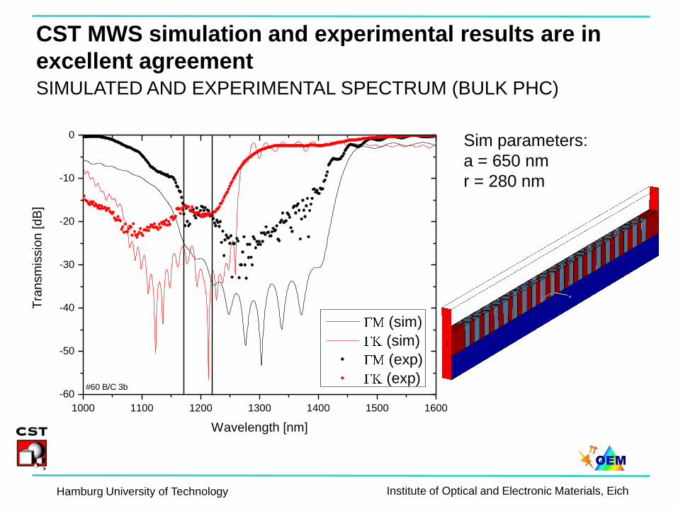
For bulk transmission behavior two transient solver
runs are necessary (ΓM and ΓK directions)
MODELS FOR TRANSMISSION OF BULK TRIANGULAR LATTICES
Same model file for both lattice directions.
Calculation by sweep of hole distances in x and z direction
ΓM
dx=a
dz=sqr(3)*a
ΓK
dx=sqr(3)*a
dz=a
Hamburg University of Technology Institute of Optical and Electronic Materials, Eich
Sim parameters:
a = 650 nm
r = 280 nm
CST MWS simulation and experimental results are in
excellent agreementSIMULATED AND EXPERIMENTAL SPECTRUM (BULK PHC)
1000 1100 1200 1300 1400 1500 1600
-60
-50
-40
-30
-20
-10
0
Tra
nsm
issio
n [dB
]
Wavelength [nm]
(sim)
(sim)
(exp)
(exp)#60 B/C 3b
Hamburg University of Technology Institute of Optical and Electronic Materials, Eich
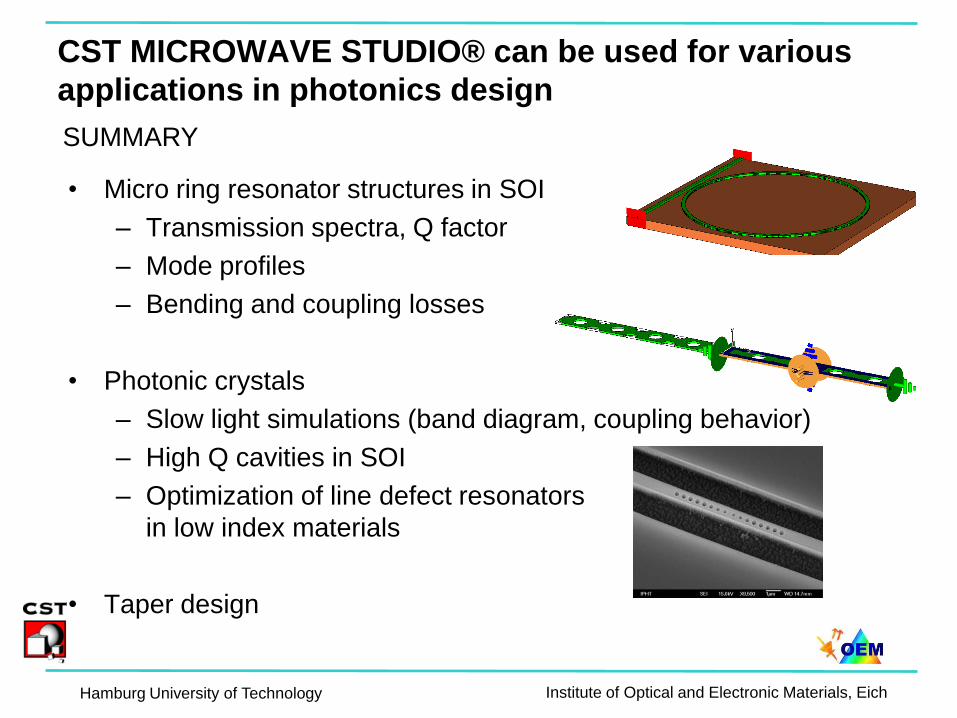
CST MICROWAVE STUDIO® can be used for various
applications in photonics design
SUMMARY
• Micro ring resonator structures in SOI
– Transmission spectra, Q factor
– Mode profiles
– Bending and coupling losses
• Photonic crystals
– Slow light simulations (band diagram, coupling behavior)
– High Q cavities in SOI
– Optimization of line defect resonators
in low index materials
• Taper design

专注于微波、射频、天线设计人才的培养 易迪拓培训 网址:http://www.edatop.com
C S T 视 频 培 训 课 程 推 荐
CST 微波工作室(CST Microwave Studio)是 CST 工作室套装中最核心的一个子软件,主要用于三维
电磁问题的仿真分析,可计算任意结构任意材料电大宽带的电磁问题。广泛应用于高频/微波无源器件
的仿真设计、各种类型的天线设计、雷达散射截面分析、电磁兼容分析和信号完整性分析等各个方面。
易迪拓培训(www.edatop.com)推出的 CST 微波工作室视频培训课程由经验丰富的专家授课,旨在
帮助用户能够快速地学习掌握 CST 微波工作室的各项功能、使用操作和工程应用。购买 CST 教学视
频培训课程套装,还可超值赠送 3 个月免费在线学习答疑,让您学习无忧。
CST 学习培训课程套装
该培训套装由易迪拓培训联合微波 EDA 网共同推出,是最全面、系统、
专业的 CST 微波工作室培训课程套装,所有课程都由经验丰富的专家
授课,视频教学,可以帮助您从零开始,全面系统地学习 CST 微波工
作的各项功能及其在微波射频、天线设计等领域的设计应用。且购买该
套装,还可超值赠送 3 个月免费学习答疑…
课程网址:http://www.edatop.com/peixun/cst/24.html
HFSS 天线设计培训课程套装
套装共含 5 门视频培训课程,课程从基础讲起,内容由浅入深,理论
介绍和实际操作讲解相结合,全面系统的讲解了 CST 微波工作室天线
设计的全过程。是国内最全面、最专业的 CST 天线设计课程,可以帮
助您快速学习掌握如何使用 CST 设计天线,让天线设计不再难…
课程网址:http://www.edatop.com/peixun/cst/127.html
更多 CST 视频培训课程:
CST 微波工作室入门与应用详解 — 中文视频教程
CST 微波工作室初学者的最佳培训课程,由工程经验丰富的资深专家授课,全程中文讲解,高清
视频,直观易学。网址:http://www.edatop.com/peixun/cst/25.html
CST 微波工作室天线设计详解 — 中文视频培训教程
重点讲解天线设计相关知识和使用 CST 进行天线仿真设计的使用操作,是学习掌握使用 CST 微
波工作室进行天线设计的必备课程,网址:http://www.edatop.com/peixun/cst/26.html
CST 阵列天线仿真设计实例详解 —— 中文视频教程
阵列天线设计专业性要求很高,因此相关培训课程是少之又少,该门培训课程由易迪拓培训重金
聘请专家讲解;课程网址:http://www.edatop.com/peixun/cst/123.html
更多 CST 培训课程,敬请浏览:http://www.edatop.com/peixun/cst

`
专注于微波、射频、天线设计人才的培养 易迪拓培训 网址:http://www.edatop.com
关于易迪拓培训:
易迪拓培训(www.edatop.com)由数名来自于研发第一线的资深工程师发起成立,一直致力和专注
于微波、射频、天线设计研发人才的培养;后于 2006 年整合合并微波 EDA 网(www.mweda.com),
现已发展成为国内最大的微波射频和天线设计人才培养基地,成功推出多套微波射频以及天线设计相
关培训课程和 ADS、HFSS 等专业软件使用培训课程,广受客户好评;并先后与人民邮电出版社、电
子工业出版社合作出版了多本专业图书,帮助数万名工程师提升了专业技术能力。客户遍布中兴通讯、
研通高频、埃威航电、国人通信等多家国内知名公司,以及台湾工业技术研究院、永业科技、全一电
子等多家台湾地区企业。
我们的课程优势:
※ 成立于 2004 年,10 多年丰富的行业经验
※ 一直专注于微波射频和天线设计工程师的培养,更了解该行业对人才的要求
※ 视频课程、既能达到现场培训的效果,又能免除您舟车劳顿的辛苦,学习工作两不误
※ 经验丰富的一线资深工程师讲授,结合实际工程案例,直观、实用、易学
联系我们:
※ 易迪拓培训官网:http://www.edatop.com
※ 微波 EDA 网:http://www.mweda.com
※ 官方淘宝店:http://shop36920890.taobao.com
专注于微波、射频、天线设计人才的培养
官方网址:http://www.edatop.com 易迪拓培训 淘宝网店:http://shop36920890.taobao.com
Related Documents