BAPATLA ENGINEERINGCOLLEGE MICROWAVE AND OPTICAL COMMUNICATIONS LAB- (EC462) PREPARED BY Smt. D.SWETHA Lecturer Department of Electronics and Communications Engineering Bapatla Engineering College (Affiliated to Acharya Nagarjuna University) Bapatla-522101 2009-2010 footer

Welcome message from author
This document is posted to help you gain knowledge. Please leave a comment to let me know what you think about it! Share it to your friends and learn new things together.
Transcript
BAPATLA ENGINEERINGCOLLEGE
MICROWAVE AND OPTICAL
COMMUNICATIONS LAB- (EC462)
PREPARED BY
Smt. D.SWETHA Lecturer
Department of Electronics and Communications Engineering Bapatla Engineering College
(Affiliated to Acharya Nagarjuna University) Bapatla-522101
2009-2010
footer
EC461 MWR&OC lab
2
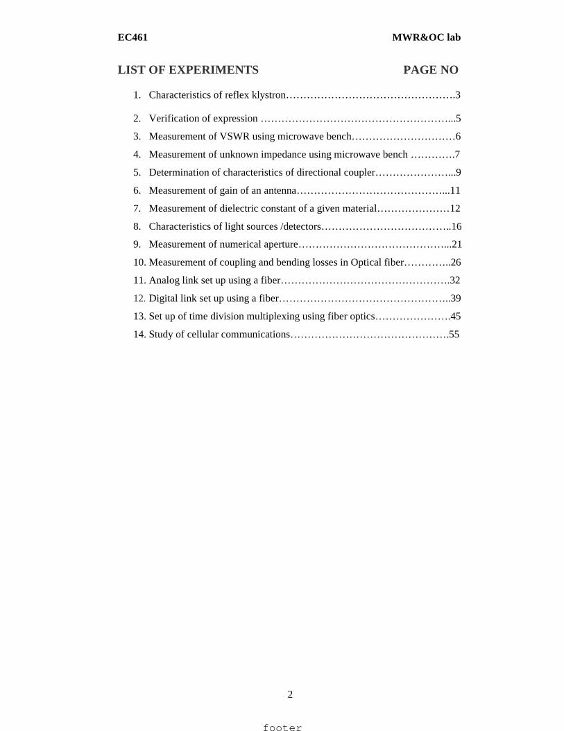
LIST OF EXPERIMENTS PAGE NO
1. Characteristics of reflex klystron………………………………………….3
2. Verification of expression ………………………………………………...5
3. Measurement of VSWR using microwave bench…………………………6
4. Measurement of unknown impedance using microwave bench ………….7
5. Determination of characteristics of directional coupler…………………...9
6. Measurement of gain of an antenna……………………………………...11
7. Measurement of dielectric constant of a given material…………………12
8. Characteristics of light sources /detectors………………………………..16
9. Measurement of numerical aperture……………………………………...21
10. Measurement of coupling and bending losses in Optical fiber…………..26
11. Analog link set up using a fiber………………………………………….32
12. Digital link set up using a fiber…………………………………………..39
13. Set up of time division multiplexing using fiber optics………………….45
14. Study of cellular communications……………………………………….55
footer
EC461 MWR&OC lab
3
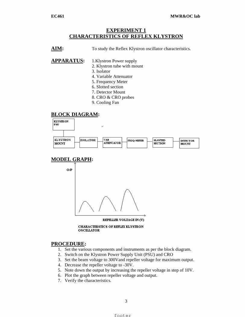
EXPERIMENT 1 CHARACTERISTICS OF REFLEX KLYSTRON
AIM : To study the Reflex Klystron oscillator characteristics. APPARATUS: 1.Klystron Power supply 2. Klystron tube with mount 3. Isolator 4. Variable Attenuator 5. Frequency Meter 6. Slotted section 7. Detector Mount 8. CRO & CRO probes 9. Cooling Fan BLOCK DIAGRAM :
MODEL GRAPH :
PROCEDURE:
1. Set the various components and instruments as per the block diagram. 2. Switch on the Klystron Power Supply Unit (PSU) and CRO 3. Set the beam voltage to 300Vand repeller voltage for maximum output. 4. Decrease the repeller voltage to -30V. 5. Note down the output by increasing the repeller voltage in step of 10V. 6. Plot the graph between repeller voltage and output. 7. Verify the characteristics.
footer

EC461 MWR&OC lab
4
PRECAUTIONS: 1. Beam voltage should be minimum and repeller voltage should be normal
before switch ON/OFF the Klystron PSU. RESULT: The characteristics of Reflex Klystron are verified.
footer

EC461 MWR&OC lab
5
EXPERIMENT 2 VERIFICATION OF EXPRESSION
AIM : To verify the expression 222 /1/1/1 cgm λλλ +=
APPARATUS: 1.Klystron Power supply 2. Klystron tube with mount 3. Isolator 4. Variable Attenuator 5. Frequency Meter 6. Slotted section 7. Detector Mount 8. CRO & CRO probes 9. Cooling Fan BLOCK DIAGRAM :
PROCEDURE:
1. Set the various components and instruments as per the block diagram. 2. Switch on the Klystron Power Supply Unit (PSU) and CRO 3. Set the beam voltage to 300Vand repeller voltage for maximum output. 4. Find the frequency of oscillation by observing the dip of waveform by
rotating the frequency meter i.e., f0 by that we can find out the λ0. 5. Find the cut-off wavelength of the waveguide λc by the relation λc=2a
where a is the hallow dimension of the waveguide. 6. Find the guide wavelength by the relation λg=2(d2-d1) where (d2-d1) is the
distance between two minimas. It is obtained by varying slotted section. 7. Verify the equation.
PRECAUTIONS: 1. Beam voltage should be minimum and repeller voltage should be normal
before switch ON/OFF the Klystron PSU. RESULT:
The expression 222 /1/1/1 cgm λλλ += is verified.
footer
EC461 MWR&OC lab
6
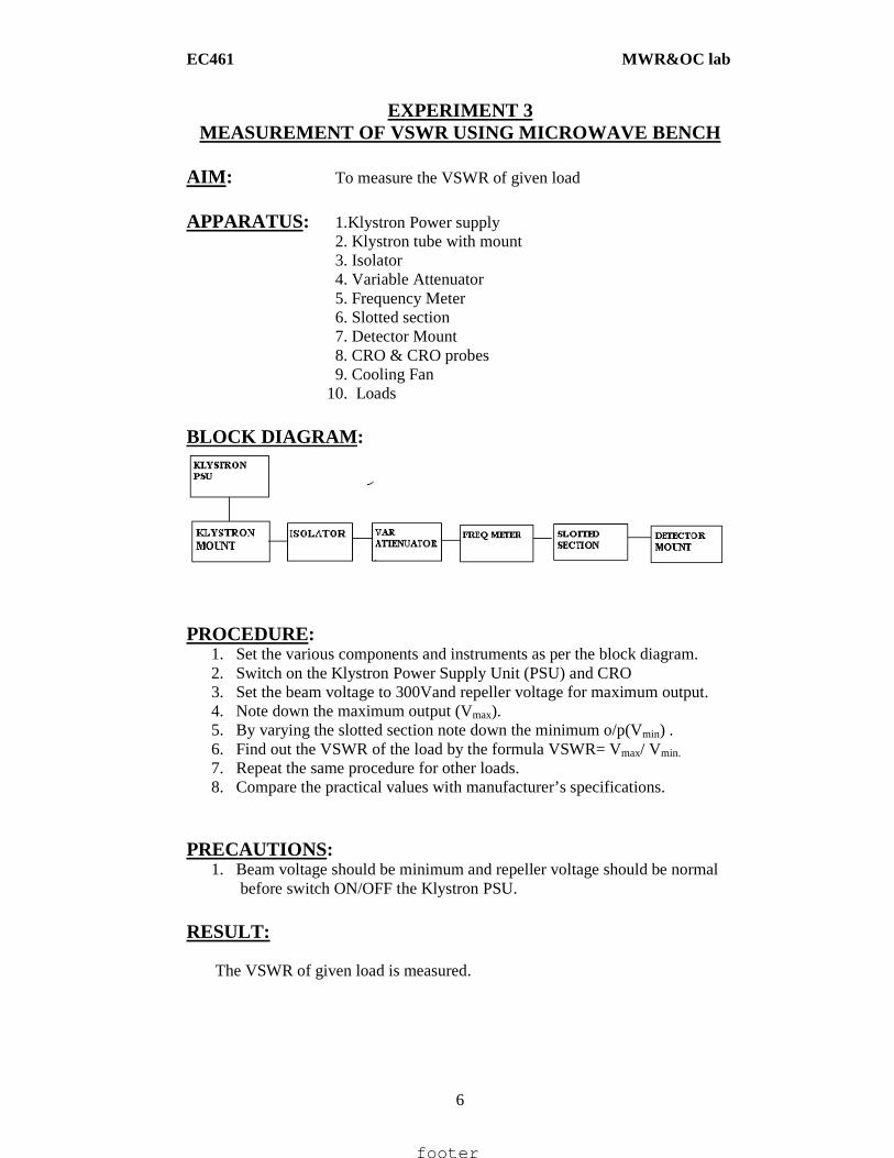
EXPERIMENT 3 MEASUREMENT OF VSWR USING MICROWAVE BENCH
AIM : To measure the VSWR of given load APPARATUS: 1.Klystron Power supply 2. Klystron tube with mount 3. Isolator 4. Variable Attenuator 5. Frequency Meter 6. Slotted section 7. Detector Mount 8. CRO & CRO probes 9. Cooling Fan 10. Loads BLOCK DIAGRAM :
PROCEDURE:
1. Set the various components and instruments as per the block diagram. 2. Switch on the Klystron Power Supply Unit (PSU) and CRO 3. Set the beam voltage to 300Vand repeller voltage for maximum output. 4. Note down the maximum output (Vmax). 5. By varying the slotted section note down the minimum o/p(Vmin) . 6. Find out the VSWR of the load by the formula VSWR= Vmax/ Vmin. 7. Repeat the same procedure for other loads. 8. Compare the practical values with manufacturer’s specifications.
PRECAUTIONS:
1. Beam voltage should be minimum and repeller voltage should be normal before switch ON/OFF the Klystron PSU.
RESULT: The VSWR of given load is measured.
footer
EC461 MWR&OC lab
7
EXPERIMENT 4 MEASUREMENT OF UNKNOWN IMPEDANCE USING
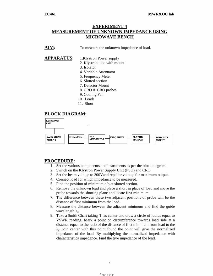
MICROWAVE BENCH AIM : To measure the unknown impedance of load. APPARATUS: 1.Klystron Power supply 2. Klystron tube with mount 3. Isolator 4. Variable Attenuator 5. Frequency Meter 6. Slotted section 7. Detector Mount 8. CRO & CRO probes 9. Cooling Fan 10. Loads 11. Short BLOCK DIAGRAM :
PROCEDURE:
1. Set the various components and instruments as per the block diagram. 2. Switch on the Klystron Power Supply Unit (PSU) and CRO 3. Set the beam voltage to 300Vand repeller voltage for maximum output. 4. Connect load for which impedance to be measured. 5. Find the position of minimum o/p at slotted section. 6. Remove the unknown load and place a short in place of load and move the
probe towards the shorting plane and locate first minimum. 7. The difference between these two adjacent positions of probe will be the
distance of first minimum from the load. 8. Measure the distance between the adjacent minimum and find the guide
wavelength λg. 9. Take a Smith Chart taking ‘l’ as center and draw a circle of radius equal to
VSWR reading. Mark a point on circumference towards load side at a distance equal to the ratio of the distance of first minimum from load to the λg .Join center with this point found the point will give the normalized impedance of the load. By multiplying the normalized impedance with characteristics impedance. Find the true impedance of the load.
footer

EC461 MWR&OC lab
8
PRECAUTIONS: 1. Beam voltage should be minimum and repeller voltage should be normal
before switch ON/OFF the Klystron PSU. RESULT: The unknown impedance of given load is measured.
footer
EC461 MWR&OC lab
9
EXPERIMENT 5 DETERMINATION OF CHARACTERISTICS OF
DIRECTIONAL COUPLER AIM : To measure the coupling factor and directivity of given
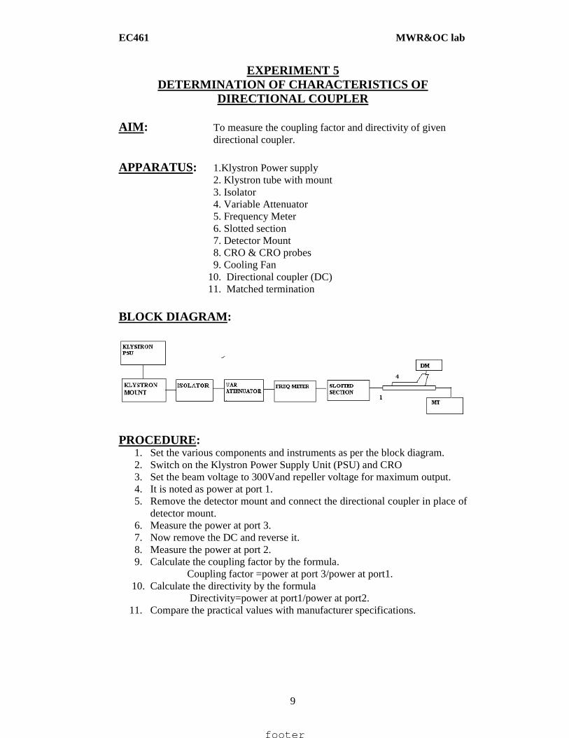
directional coupler. APPARATUS: 1.Klystron Power supply 2. Klystron tube with mount 3. Isolator 4. Variable Attenuator 5. Frequency Meter 6. Slotted section 7. Detector Mount 8. CRO & CRO probes 9. Cooling Fan 10. Directional coupler (DC) 11. Matched termination BLOCK DIAGRAM :
PROCEDURE:
1. Set the various components and instruments as per the block diagram. 2. Switch on the Klystron Power Supply Unit (PSU) and CRO 3. Set the beam voltage to 300Vand repeller voltage for maximum output. 4. It is noted as power at port 1. 5. Remove the detector mount and connect the directional coupler in place of
detector mount. 6. Measure the power at port 3. 7. Now remove the DC and reverse it. 8. Measure the power at port 2. 9. Calculate the coupling factor by the formula. Coupling factor =power at port 3/power at port1.
10. Calculate the directivity by the formula Directivity=power at port1/power at port2.
11. Compare the practical values with manufacturer specifications.
footer

EC461 MWR&OC lab
10
PRECAUTIONS: 1. Beam voltage should be minimum and repeller voltage should be normal
before switch ON/OFF the Klystron PSU. RESULT: The coupling factor and directivity of given directional coupler are measured.
footer
EC461 MWR&OC lab
11
EXPERIMENT 6 MEASUREMENT OF GAIN OF AN ANTENNA
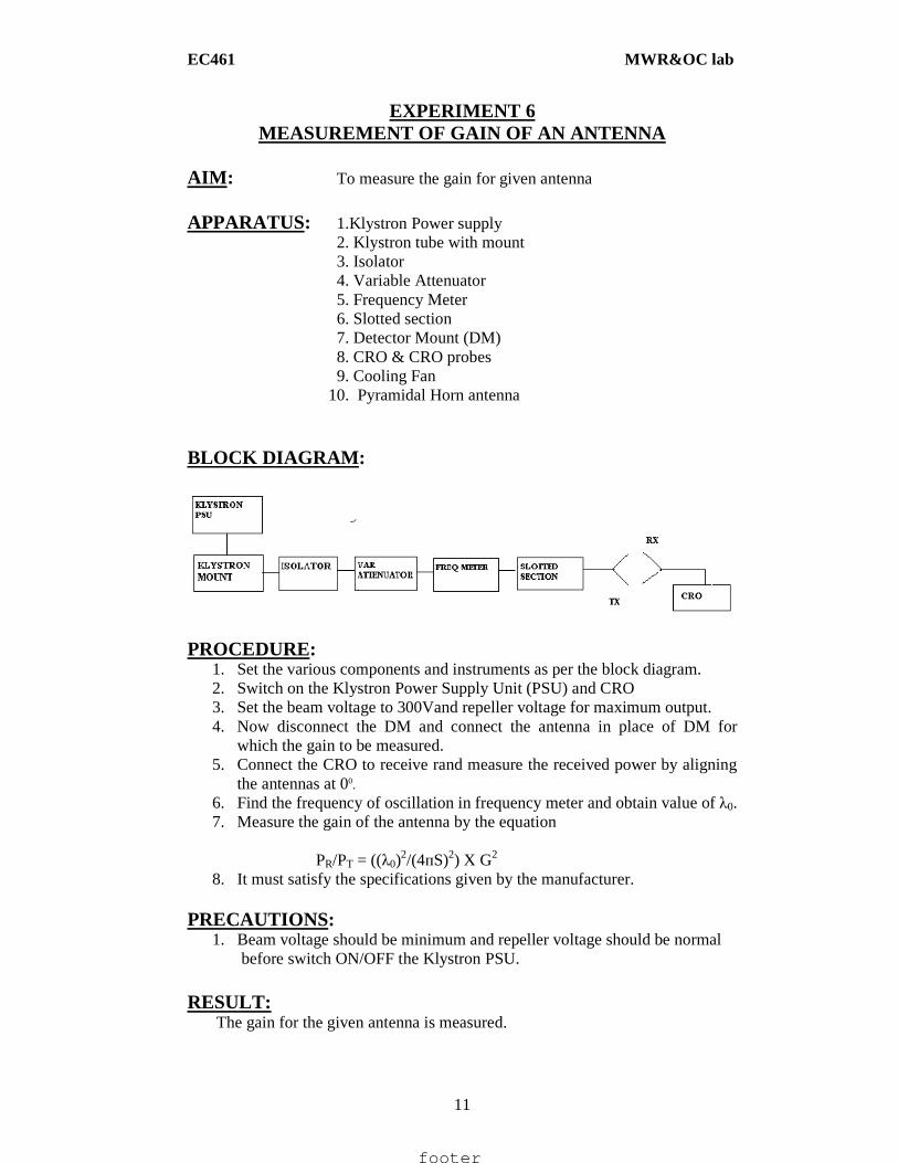
AIM : To measure the gain for given antenna APPARATUS: 1.Klystron Power supply 2. Klystron tube with mount 3. Isolator 4. Variable Attenuator 5. Frequency Meter 6. Slotted section 7. Detector Mount (DM) 8. CRO & CRO probes 9. Cooling Fan 10. Pyramidal Horn antenna BLOCK DIAGRAM :
PROCEDURE:
1. Set the various components and instruments as per the block diagram. 2. Switch on the Klystron Power Supply Unit (PSU) and CRO 3. Set the beam voltage to 300Vand repeller voltage for maximum output. 4. Now disconnect the DM and connect the antenna in place of DM for
which the gain to be measured. 5. Connect the CRO to receive rand measure the received power by aligning
the antennas at 00. 6. Find the frequency of oscillation in frequency meter and obtain value of λ0. 7. Measure the gain of the antenna by the equation PR/PT = ((λ0)
2/(4пS)2) X G2 8. It must satisfy the specifications given by the manufacturer.
PRECAUTIONS:
1. Beam voltage should be minimum and repeller voltage should be normal before switch ON/OFF the Klystron PSU.
RESULT: The gain for the given antenna is measured.
footer
EC461 MWR&OC lab
12
EXPERIMENT 7 MEASUREMENT OF DIELECTRIC CONSTANT OF A GIVEN
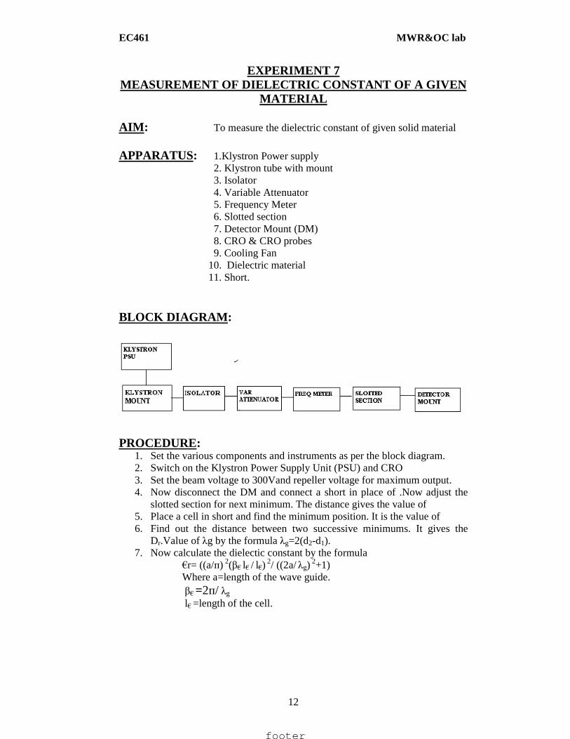
MATERIAL AIM : To measure the dielectric constant of given solid material APPARATUS: 1.Klystron Power supply 2. Klystron tube with mount 3. Isolator 4. Variable Attenuator 5. Frequency Meter 6. Slotted section 7. Detector Mount (DM) 8. CRO & CRO probes 9. Cooling Fan 10. Dielectric material 11. Short. BLOCK DIAGRAM :
PROCEDURE:
1. Set the various components and instruments as per the block diagram. 2. Switch on the Klystron Power Supply Unit (PSU) and CRO 3. Set the beam voltage to 300Vand repeller voltage for maximum output. 4. Now disconnect the DM and connect a short in place of .Now adjust the
slotted section for next minimum. The distance gives the value of 5. Place a cell in short and find the minimum position. It is the value of 6. Find out the distance between two successive minimums. It gives the
Dr.Value of λg by the formula λg=2(d2-d1). 7. Now calculate the dielectic constant by the formula
€r= ((a/п) 2(β€ l€ / l€) 2/ ((2a/ λg)
2+1) Where a=length of the wave guide.
β€ =2п/ λg
l€ =length of the cell.
footer

EC461 MWR&OC lab
13
PRECAUTIONS: 1. Beam voltage should be minimum and repeller voltage should be normal before switch ON/OFF the Klystron PSU.
RESULT: The dielectric constant of given solid material is measured.
footer
EC461 MWR&OC lab
14
INTRODUCTION TO OPTICAL COMMUNICATIONS
An optical fiber is a dielectric wave guide through which light can be transmitted by total internal reflection. Usually optical fibers are flexible, thin, and cylindrical and made of transparent materials such as glass and plastic. The most abundant and widespread material used to make optical fiber is glass and most often this is an oxide glass based on silica (SiO2) with some additives.
There are three types of fiber optic cables: single mode, multimode and plastic optical fiber (POF).Single Mode cable is a single stand of glass fiber with a diameter of 8.3 to 10 microns. (One micron is 1/250th the width of a human hair.) Multimode cable is made of multiple strands of glass fibers, with a combined diameter in the 50-to-100 micron range. Each fiber in a multimode cable is capable of carrying a different signal independent from those on the other fibers in the cable bundle. POF is a newer plastic-based cable which promises performance similar to single mode cable, but at a lower cost.
PRINCIPLES OF FIBER OPTICS :
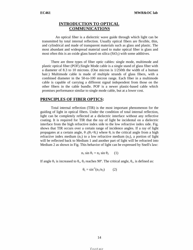
Total internal reflection (TIR) is the most important phenomenon for the guiding of light in optical fibers. Under the condition of total internal reflection, light can be completely reflected at a dielectric interface without any reflective coating. It is required for TIR that the ray of light be incidental on a dielectric interface from the high refractive index side to the low refractive index side. Fig. shows that TIR occurs over a certain range of incidence angles. If a ray of light propagates at a certain angle, θ 1(θ1<θc) where θc is the critical angle from a high refractive index medium (n1) to a low refractive medium (n2), a portion of light will be reflected back to Medium 1 and another part of light will be refracted into Medium 2 as shown in Fig. This behavior of light can be expressed by Snell's law:
n1 sin θ1 = n2 sin θ2 (1)
If angle θ1 is increased to θc, θ2 reaches 90º. The critical angle, θc, is defined as:
θc = sin-1(n1/n2) (2)
footer
EC461 MWR&OC lab
15
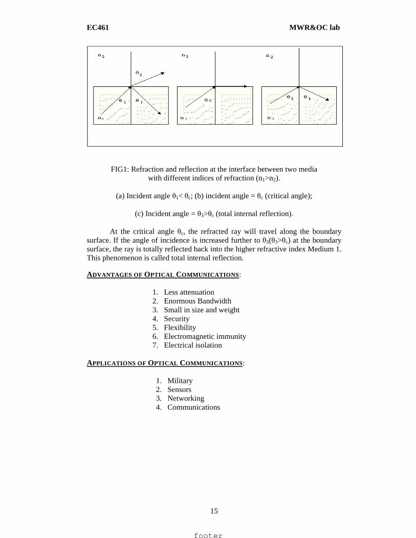
FIG1: Refraction and reflection at the interface between two media with different indices of refraction (n1>n2).
(a) Incident angle θ1< θc; (b) incident angle = θc (critical angle);
(c) Incident angle = θ3>θc (total internal reflection).
At the critical angle θc, the refracted ray will travel along the boundary surface. If the angle of incidence is increased further to θ3(θ3>θc) at the boundary surface, the ray is totally reflected back into the higher refractive index Medium 1. This phenomenon is called total internal reflection.
ADVANTAGES OF OPTICAL COMMUNICATIONS :
1. Less attenuation 2. Enormous Bandwidth 3. Small in size and weight 4. Security 5. Flexibility 6. Electromagnetic immunity 7. Electrical isolation
APPLICATIONS OF OPTICAL COMMUNICATIONS :
1. Military 2. Sensors 3. Networking 4. Communications
footer
EC461 MWR&OC lab
16
EXPERIMENT 8 CHARACTERISTICS OF LIGHT SOURCES /DETECTORS
PART-A: CHARACTERISTICS OF LED: Aim: To study the relationship between the optical power output and dc forward current of LED and determine the linearity of the device at 660 nm as well as 850 nm. APPARATUS:
1. LED TX Kit - λ=660 nm& 850 nm 2. LED RX Kit - λ=660 nm& 850 nm 3. Multimeter 4. Optical Fiber Cable - PMMA Type 5. CRO - 30 MHz
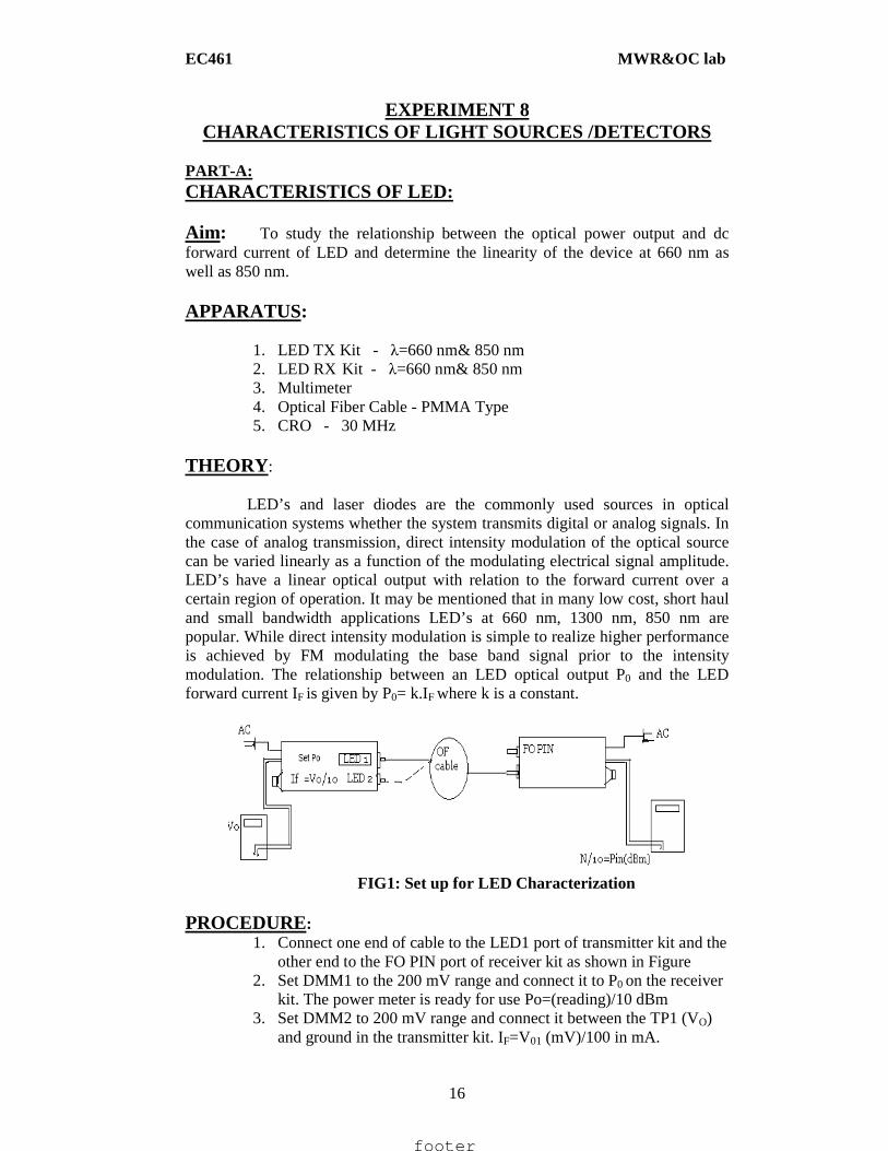
THEORY : LED’s and laser diodes are the commonly used sources in optical communication systems whether the system transmits digital or analog signals. In the case of analog transmission, direct intensity modulation of the optical source can be varied linearly as a function of the modulating electrical signal amplitude. LED’s have a linear optical output with relation to the forward current over a certain region of operation. It may be mentioned that in many low cost, short haul and small bandwidth applications LED’s at 660 nm, 1300 nm, 850 nm are popular. While direct intensity modulation is simple to realize higher performance is achieved by FM modulating the base band signal prior to the intensity modulation. The relationship between an LED optical output P0 and the LED forward current IF is given by P0= k.IF where k is a constant.
FIG1: Set up for LED Characterization PROCEDURE:
1. Connect one end of cable to the LED1 port of transmitter kit and the other end to the FO PIN port of receiver kit as shown in Figure
2. Set DMM1 to the 200 mV range and connect it to P0 on the receiver kit. The power meter is ready for use Po=(reading)/10 dBm
3. Set DMM2 to 200 mV range and connect it between the TP1 (VO) and ground in the transmitter kit. IF=V01 (mV)/100 in mA.
footer
EC461 MWR&OC lab
17
4. Plug the AC mains for both units. Adjust the set gain knob on the transmitter kit to the extreme anticlockwise position to reduce IF to minimum. The reading on the power meter should be out of range.
5. Slowly turn the set gain knob clockwise to increase IF. The power meter should read –30.0 dB approximately. From here change IF in suitable steps and note the power meter readings P0.
6. Record up to the extreme clockwise position. 7. Plot a graph between P0 and IF as shown in the Fig 2.
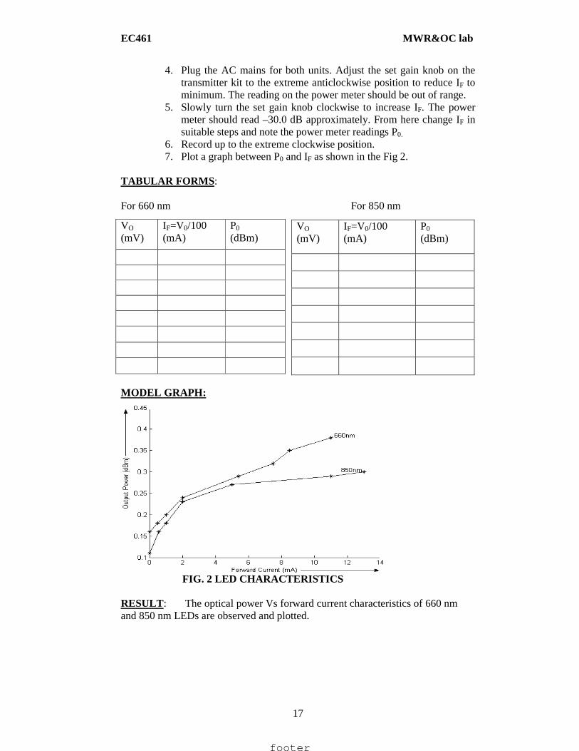
TABULAR FORMS : For 660 nm For 850 nm
MODEL GRAPH:
FIG. 2 LED CHARACTERISTICS RESULT: The optical power Vs forward current characteristics of 660 nm and 850 nm LEDs are observed and plotted.
VO (mV)
IF=V0/100 (mA)
P0 (dBm)
VO (mV)
IF=V0/100 (mA)
P0 (dBm)
footer
EC461 MWR&OC lab
18
PART-B: CHARACTERISTICS OF LASER DIODE: AIM : To find the characteristics of Optical Power (Po) of laser diode vs. Laser diode forward current (IF). APPARATUS:
1. LD TX Kit - λ=660 nm 2. LED RX Kit - λ=660 nm 3. Multimeter 4. Optical Fiber Cable - PMMA Type 5. CRO - 30 MHz
THEORY : Laser diodes (LDs) are used in telecom, data, and video communication applications involving high speeds and long hauls. All single mode optical fiber communication systems use lasers in the 1300 nm and 1500 nm windows. Lasers with very small line-widths also facilitate realization of wavelength division multiplexing (WDM) for high density communication over a single fiber. The inherent properties of LDs that make them suitable for such applications are, high coupled optical power in to the fiber (typically greater than 1mw), high stability of optical intensity, small line-widths (less than 0.05 nm in special devices), high speed (several GHz) and high linearity (over a specified region suitable for analog transmission) special lasers also provide for regeneration / amplification of optical signals within an optical fiber. These fibers are known as erbium doped fiber amplifiers (EDPA). Specifications of a typical laser diode are given in Appendix B.Even though a variety of laser diode constructions are available there are a number of common features in all of them . Very simple device (650nm /2.5mw )is used to demonstrate the functioning of a laser diode A laser diode has a built – in photo detector ,which one can employ to monitor the optical intensity of the laser at a specified forward current . This device is also effectively utilized in designing an optical negative feedback control loop , to stabilize the optical power of a laser in the steep lasing region . The electronic circuit scheme that employs the monitor photo diode to provide a negative feedback for stabilization of optical power is known as the automatic power control mode (APC) . If a closed loop employs current control alone to set optical power then this mode is called the automatic current control mode (ACC) . The disadvantage of ACC scheme is that the optical power output may not be stable at a given current due to the fact that small shifts in the lasing characteristics occur with temperature changes and ageing . The disadvantage of the APC is that the optical feedback loop may cause oscillations , if not designed properly .
footer
EC461 MWR&OC lab
19
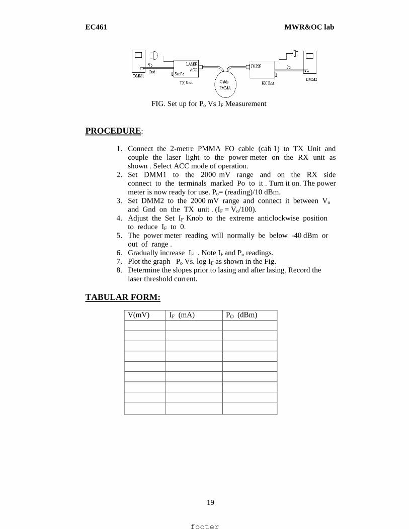
FIG. Set up for Po Vs IF Measurement PROCEDURE:
1. Connect the 2-metre PMMA FO cable (cab 1) to TX Unit and couple the laser light to the power meter on the RX unit as shown . Select ACC mode of operation.
2. Set DMM1 to the 2000 mV range and on the RX side connect to the terminals marked Po to it . Turn it on. The power meter is now ready for use. Po= (reading)/10 dBm.
3. Set DMM2 to the 2000 mV range and connect it between Vo and Gnd on the TX unit . (IF = Vo/100).
4. Adjust the Set IF Knob to the extreme anticlockwise position to reduce IF to 0.
5. The power meter reading will normally be below -40 dBm or out of range .
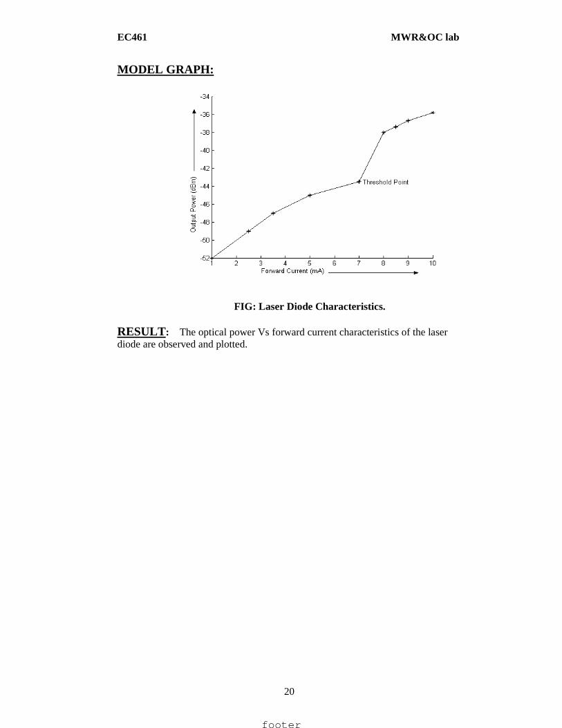
6. Gradually increase IF . Note IF and Po readings. 7. Plot the graph Po Vs. log IF as shown in the Fig. 8. Determine the slopes prior to lasing and after lasing. Record the
laser threshold current. TABULAR FORM:
V(mV) IF (mA) PO (dBm)
footer
EC461 MWR&OC lab
20
MODEL GRAPH:
FIG: Laser Diode Characteristics. RESULT: The optical power Vs forward current characteristics of the laser diode are observed and plotted.
footer
EC461 MWR&OC lab
21
EXPERIMENT 9 MEASUREMENT OF NUMERICAL APERTURE
AIM : To estimate the Numerical Aperture of the 1mm diameter plastic fiber at 650 nm. APPARATUS: 1.OFT Trainer Kit 2. Numerical Aperture Measurement Unit 3. 1mm diameter 1m fiber THEORY :
Numerical aperture of the fiber is a measure of the acceptance angle of light in the fiber. Light which is launched at angles greater than this maximum acceptable angle does not get coupled to propagating modes in the fiber, and therefore does not reach the receiver at other end of the fiber. The NA is useful in the computation of optical power coupled from an optical source to the fiber, from fiber to a photo detector, and between two fibers. PROCEDURE: SETUP:
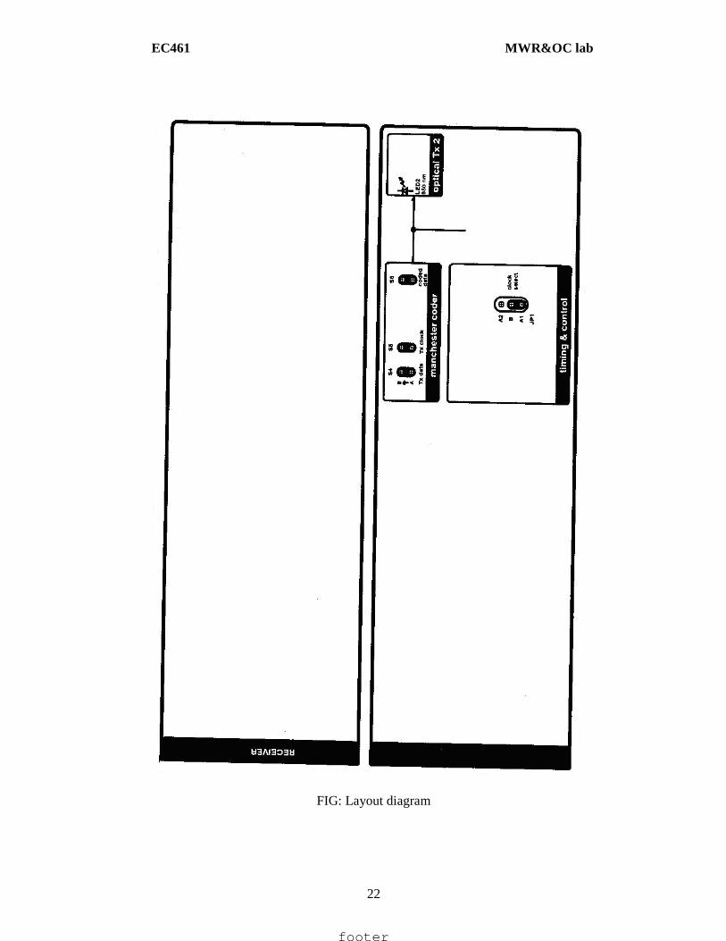
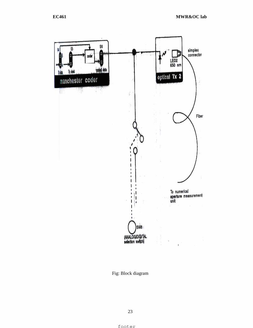
1. The interfaces used in the experiment are summarized in Table. Identify them on OFT kit with the layout diagram. The block diagram is shown in fig. ensure that the shorting plugs of Tx data shorting link S4, coded data shorting link S6, and Tx clock shorting link S5 in the Manchester coder block are in position. Also ensure that the shorting plug of clock select jumper JP1 is across the posts B&A1. A TTL signal from the multiplexer should now be driving LED2 in optical Tx2 block. This experiment is best performed in a less illuminated room.
2. Ensure that the cut planes of the 1m plastic fiber are perpendicular to the axis of the fiber. If required, prepare 1m of plastic fiber as per the instructions in appendix A.
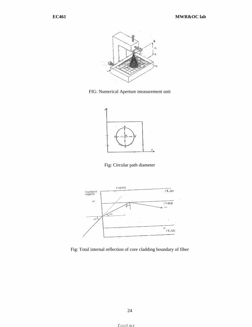
3. Insert one end of fiber in to NA measurement unit as shown in figure. adjust the fiber such that its tip is 10mm from the screen.
4. Gently tighten the screw to hold the fiber firmly in place. 5. Connect the other end of the fiber to LED2 through the simplex
connector. The fiber will project a circular patch of red light on to the screen. Now measure the diameter of the circular patch of red light in two perpendicular directions (BC and DE in Fig). the mean radius of the circular patch is given by
X = (DE +BC)/4
6. Carefully measure the distance d between the tip of the fiber and the illuminated screen (OA in Fig). The Numerical Aperture of the fiber is given by
NA = Sin (Ө) =X/ (√ (d2+X2)
7. Repeat steps 3 to 6 for different values of d. compute the average value
of Numerical aperture.
footer
EC461 MWR&OC lab
22
FIG: Layout diagram
footer
EC461 MWR&OC lab
23
Fig: Block diagram
footer
EC461 MWR&OC lab
24
FIG: Numerical Aperture measurement unit
Fig: Circular path diameter
Fig: Total internal reflection of core cladding boundary of fiber
footer
EC461 MWR&OC lab
25
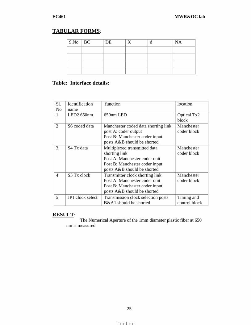
TABULAR FORMS :
S.No BC DE X d NA
Table: Interface details:
RESULT:
The Numerical Aperture of the 1mm diameter plastic fiber at 650 nm is measured.
Sl.No
Identification name
function location
1 LED2 650nm 650nm LED Optical Tx2 block
2 S6 coded data Manchester coded data shorting link post A: coder output Post B: Manchester coder input posts A&B should be shorted
Manchester coder block
3 S4 Tx data Multiplexed transmitted data shorting link Post A: Manchester coder unit Post B: Manchester coder input posts A&B should be shorted
Manchester coder block
4 S5 Tx clock Transmitter clock shorting link Post A: Manchester coder unit Post B: Manchester coder input posts A&B should be shorted
Manchester coder block
5 JP1 clock select Transmission clock selection posts B&A1 should be shorted
Timing and control block
footer
EC461 MWR&OC lab
26
EXPERIMENT 10 MEASUREMENT OF COUPLING AND BENDING LOSSES IN
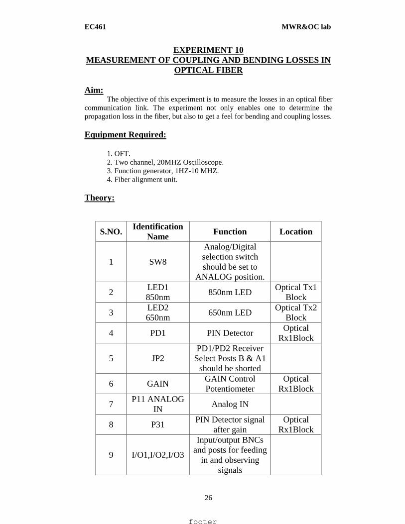
OPTICAL FIBER Aim: The objective of this experiment is to measure the losses in an optical fiber communication link. The experiment not only enables one to determine the propagation loss in the fiber, but also to get a feel for bending and coupling losses. Equipment Required: 1. OFT. 2. Two channel, 20MHZ Oscilloscope. 3. Function generator, 1HZ-10 MHZ. 4. Fiber alignment unit. Theory:
S.NO. Identification
Name Function Location
1 SW8
Analog/Digital selection switch should be set to
ANALOG position.
2 LED1 850nm
850nm LED Optical Tx1
Block
3 LED2 650nm
650nm LED Optical Tx2
Block
4 PD1 PIN Detector Optical
Rx1Block
5 JP2 PD1/PD2 Receiver
Select Posts B & A1 should be shorted
6 GAIN GAIN Control Potentiometer
Optical Rx1Block
7 P11 ANALOG
IN Analog IN
8 P31 PIN Detector signal
after gain Optical
Rx1Block
9 I/O1,I/O2,I/O3
Input/output BNCs and posts for feeding
in and observing signals
footer
EC461 MWR&OC lab
27
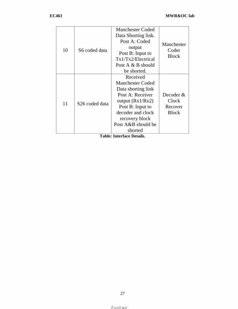
10 S6 coded data
Manchester Coded Data Shorting link.
Post A: Coded output
Post B: Input to Tx1/Tx2/Electrical Post A & B should
be shorted.
Manchester Coder Block
11 S26 coded data
Received Manchester Coded Data shorting link Post A: Receiver output (Rx1/Rx2) Post B: Input to
decoder and clock recovery block
Post A&B should be shorted
Decoder & Clock
Recover Block
Table: Interface Details.
footer
EC461 MWR&OC lab
28
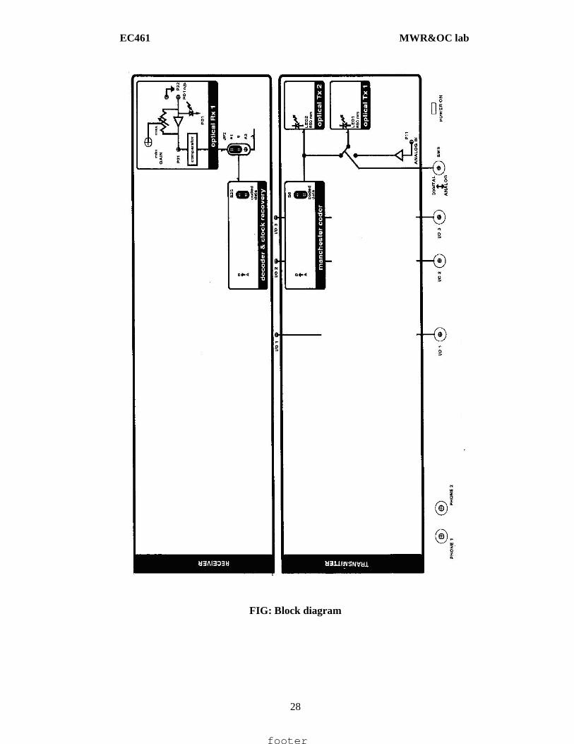
FIG: Block diagram
footer
EC461 MWR&OC lab
29
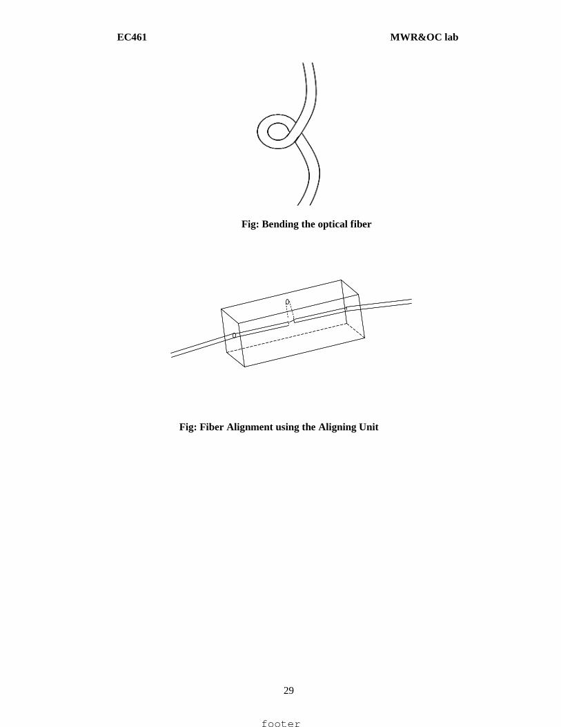
Fig: Bending the optical fiber
Fig: Fiber Alignment using the Aligning Unit
footer
EC461 MWR&OC lab
30
PROCEDURE:
1. Set the switch SW8 to the ANALOG position. Ensure that the shorting plug of the jumper JP2 is across the posts B& A1 (for PD1). Remove the shorting plugs from coded data shorting links. S6 in the Manchester coder block and S26 in the Decoder& clock recovery block.
Attenuation at 850 nm:
2. Take the 1m fiber and setup and analog link using LED1 in the Optical Tx1 block and detector PD1 in the Optical Rx1 block [850nm link]. Drive a 1V p-p 10 KHz sinusoidal signal with zero d.c. at P11. Observe the signal at P31 on the oscilloscope. Use the BNC I/Os for feeding in and observing signals. Adjust the GAIN such that the received signal is not saturated. Do not disturb the level of the signal at the function generator or the gain setting throughout the rest of the experiment.
3. Note the peak value of the signal received at P31 and designated it as V1.
Replace the 1m fiber by the 3m fiber between LED1 and PD1. Again note the peak value of the received signal and designate it as V3. If α is the attenuation in the fiber and I1 and I3 are the exact length of the 1m and 3m fibers in meters respectively, we have
[ ]131
3
1
3 (exp IIV
V
P
P−−== α
Where α is in nepers/m, and P1 and P3 are the received optical power with 1m and 3m fiber respectively. Compute α in dB/m for 850nm wavelength using α’=4.343α where α is in nepers/m.
Attenuation at 650nm:
4. Now setup the 650nm link using LED2, detector PD1 and the 1m fiber. Remove the shorting plugs from S6 and S26 and feed in a TTL signal of 10 KHz at post B of S6. Observe the signal at P31 on the oscilloscope. Adjust the GAIN such that the received signal is not saturated. Note the peak value of the 1m fiber with the 3m fiber between LED2 and PD1. Again without disturbing the GAIN, note the peak value of the received signal and designate it as V3. Compute α’ in dB/m for a 650nm wavelength using the expressions given Step3.
Bending Loss:
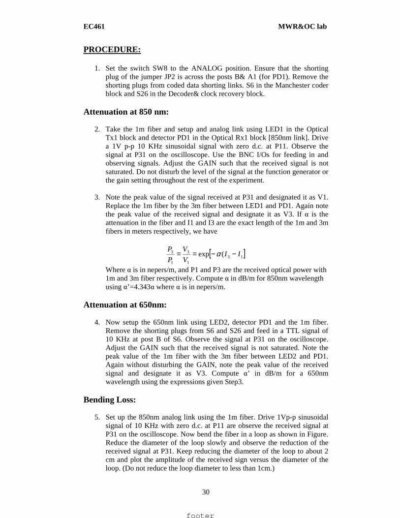
5. Set up the 850nm analog link using the 1m fiber. Drive 1Vp-p sinusoidal signal of 10 KHz with zero d.c. at P11 are observe the received signal at P31 on the oscilloscope. Now bend the fiber in a loop as shown in Figure. Reduce the diameter of the loop slowly and observe the reduction of the received signal at P31. Keep reducing the diameter of the loop to about 2 cm and plot the amplitude of the received sign versus the diameter of the loop. (Do not reduce the loop diameter to less than 1cm.)
footer
EC461 MWR&OC lab
31
Coupling Loss: 6. Connect one end of the 1m fiber to LED2 and the other end to the detector
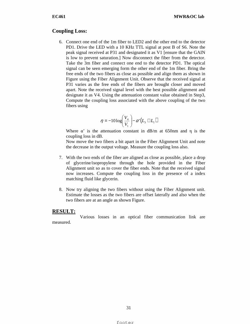
PD1. Drive the LED with a 10 KHz TTL signal at post B of S6. Note the peak signal received at P31 and designated it as V1 [ensure that the GAIN is low to prevent saturation.] Now disconnect the fiber from the detector. Take the 3m fiber and connect one end to the detector PD1. The optical signal can be seen emerging form the other end of the 1m fiber. Bring the free ends of the two fibers as close as possible and align them as shown in Figure using the Fiber Alignment Unit. Observe that the received signal at P31 varies as the free ends of the fibers are brought closer and moved apart. Note the received signal level with the best possible alignment and designate it as V4. Using the attenuation constant value obtained in Step3, Compute the coupling loss associated with the above coupling of the two fibers using
( )131
4 'log10 LLV
V+−
−= αη
Where α’ is the attenuation constant in dB/m at 650nm and η is the coupling loss in dB. Now move the two fibers a bit apart in the Fiber Alignment Unit and note the decrease in the output voltage. Measure the coupling loss also.
7. With the two ends of the fiber are aligned as close as possible, place a drop
of glycerine/isopropylene through the hole provided in the Fiber Alignment unit so as to cover the fiber ends. Note that the received signal now increases. Compute the coupling loss in the presence of a index matching fluid like glycerin.
8. Now try aligning the two fibers without using the Fiber Alignment unit.
Estimate the losses as the two fibers are offset laterally and also when the two fibers are at an angle as shown Figure.
RESULT: Various losses in an optical fiber communication link are measured.
footer
EC461 MWR&OC lab
32
EXPERIMENT 11 ANALOG LINK SET UP USING A FIBER
AIM : To set up an 850nm fiber optic analog link. The linear relationship between the input and output is observed. The effect of gain control on the received signal is also observed, and finally the bandwidth of the link is measured.
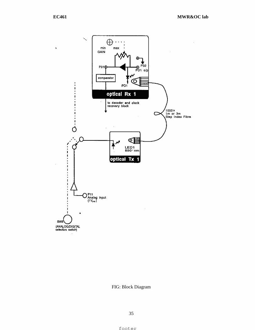
APPARATUS: 1.OFT Trainer Kit 2. CRO and CRO probes 3. Function Generator 4.1mm diameter 1m fiber THEORY: This experiment is familiarizing the user with OFT. An analog fiber optic link is to be setup in this experiment. The preparation of the optical fiber for coupling light into it and the coupling of the fiber to the LED and detector are described in appendix a. the LED used is an 850nm LED. The fiber is a multimedia fiber with a core diameter of 1000µm. the detector is a simple PIN detector.
The LED optical power output is directly proportional to the current driving the LED. Similarly for the pin diode the current is proportional to the amount of light falling on the detector. Thus even though the LED and the pin diode are non-linear devices, the current in the pin diode is directly proportional to the driving current of LED. This makes the optical communication system a linear system.
PROCEDURE: SETUP:
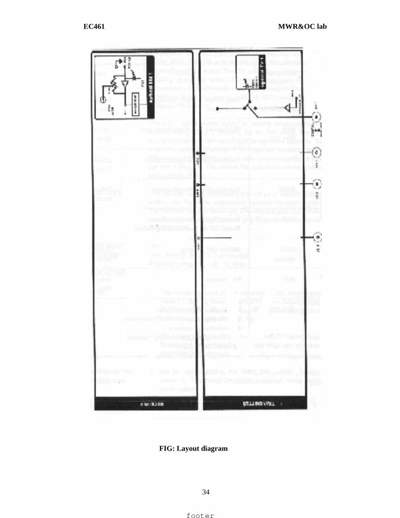
1. The interfaces used in the experiment are summarized in table. Identify them on the OFT with the help of the layout diagram (fig).the block diagram of the subsystems used in this experiment is shown in fig. The 1m and 3m optical fiber provided with OFT are used. Ensure that the ends of the fiber are clean.
Interface details S.NO Identification
name Function Location
1 P11 ANALOG IN
Used to feed in analog sinusoidal 1Vp-p signal
Tx block
2 P32 PD1O/p PINdetector signal monitoring post
Optical Rx1 block
3 P31 Received signal with amplification
Optical Rx1 block
4 GAIN Gain adjustment potentiometer
Optical Rx1 block
5 SW8 Analog/Digital selection switch Should be set to ANALOG
footer
EC461 MWR&OC lab
33
position
6 LED1 850 nm 850nm LED(source)
Optical TX1 Block
7 PD1 PIN detector Optical Rx1 block
9 l/O1,I/O2,I/O3 Input/output BNC’s and posts 1 feeding in signal to experimentor from function generator or 2 to observe signal from the experimentor the oscilloscope
SETTING UP THE ANALOG LINK :
2. Set the switch SW8 to the ANALOG position. switch the power ON the power ON switch is located at the top right hand corner. 3. Feed a 1V p-p (peak-to-peak) sinusoidal signal at 1 KHz (with zero d.c),
from a function generator, to the ANALOG IN post P11 using the following procedure. i) Connect a BNC-BNC cable from the function generator to the BNC socket I/03.
ii) Connect the signal post P11 using a patch cord. With this, the signal from the function generator is fed through to the ANALOG IN signal post P11 from the I/03 BNC Socket.
Connect one end of the 1m fiber to the LED source LED1 in the optical Tx1 block. (See Appendix A for the connection procedure).
footer
EC461 MWR&OC lab
34
FIG: Layout diagram
footer
EC461 MWR&OC lab
35
FIG: Block Diagram
footer
EC461 MWR&OC lab
36
Observe the light out put (red tinge) at the other end of the fiber.
Take care to keep the fiber at a distance from the eyes and avoid direct eye contact with the infra red radiation as it can other wise cause eye-damage.
Increase and decrease the amplitude level of sinusoidal signal (from 0V to max 2V p-p).What happens to the light out put at the other end of the fiber? To observe a fed in signal on an oscilloscope:
1. Use a three-plug patch card to connect the signal post I/03 to the required input post. Use the long half of the patch cord for this, and plug the centre plug into I/03. (Here use the 3-patch cord to connect signal post I/03 to the ANALOG IN post P11 in (ii) above instead of a regular patch cord.) 2. Connect a BNC-BNC cable between the BNC sockets I/02 and the oscilloscope. iii) Connect signal posts I/03 and I/02 together using short half of the 3-plug patch cord 4. Feed a 5V p-p rectangular signal at 0.5 Hz at P11.observe the signal on the oscilloscope. Now observe the intensity (brightness) of the light output at the other end of the fiber. Take care to keep the fiber well away from the eyes. You will notice the light turning on and off (bright and dull) as the driving signal observed on the oscilloscope becomes positive and negative. Now feed a 5V p-p sinusoidal signal at 0.5Hz at P11.Observe the variation in the brightness of the light out put at the other end of the fiber as the driving signal varies sinusoidally. Thus light intensity (brightness) is modulated by an input rectangular or sinusoidal signal. 5. Connect the other end of the fiber to the detector PD1in the optical Rx1 block. INPUT-OUTPUT RELATIONSHIP OF LINK : 6. Feed a sinusoidal wave of 1 KHz, 1V p-p [with zero dc] from the function generator to P11.the PIN detector out put signal is available at P32 in the optical Rx1 block. Vary the input signal level driving the LED and observe the received signal at the PIN detector. Plot the received signal peak-peak amplitude with respect to the input signal peak-peak amplitude. What is the relationship? 7. Repeat step 6 using the 3m fiber instead of the 1m fiber. Plot the received signal amplitude at the PIN detector as a function of input signal amplitude.
footer
EC461 MWR&OC lab
37
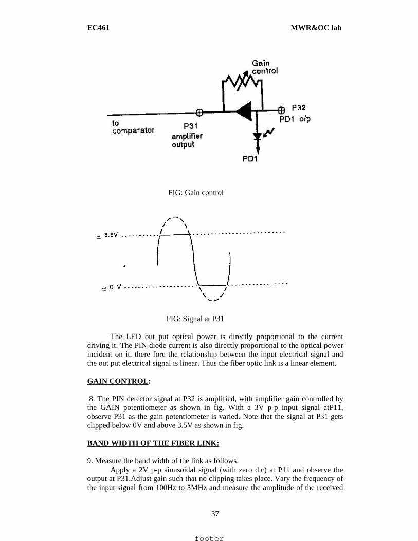
FIG: Gain control
FIG: Signal at P31 The LED out put optical power is directly proportional to the current driving it. The PIN diode current is also directly proportional to the optical power incident on it. there fore the relationship between the input electrical signal and the out put electrical signal is linear. Thus the fiber optic link is a linear element.
GAIN CONTROL : 8. The PIN detector signal at P32 is amplified, with amplifier gain controlled by the GAIN potentiometer as shown in fig. With a 3V p-p input signal atP11, observe P31 as the gain potentiometer is varied. Note that the signal at P31 gets clipped below 0V and above 3.5V as shown in fig. BAND WIDTH OF THE FIBER LINK: 9. Measure the band width of the link as follows:
Apply a 2V p-p sinusoidal signal (with zero d.c) at P11 and observe the output at P31.Adjust gain such that no clipping takes place. Vary the frequency of the input signal from 100Hz to 5MHz and measure the amplitude of the received
footer
EC461 MWR&OC lab
38
signal. Plot the received signal amplitude as a function of frequency (using a logarithmic scale for frequency).Note the frequency range for which the response is flat.
10. Apply a square wave or triangular wave with 1V p-p and zero dc at the input of the transmitter [at P11].Vary the frequency and observe the out put at P31.note the frequency at which the received signal starts getting distorted. Explain this using the band width obtained in the previous step. SUMMING UP :
You have learned the following: • to setup an analog fiber optic link • to modulate the light intensity • the relationship between the input signal driving the LED and the
received signal at the pin diode. • the band width that the link can support. • Next, we move on to setup digital fiber optic link.
footer
EC461 MWR&OC lab
39
EXPERIMENT 12 DIGITAL LINKSET UP USING A FIBER
AIM : The objective of this experiment is to learn to set up 650nm and 850nm digital links, and to measure the maximum bit rates supportable on these links. APPARATUS:
1. OFT 2. Two channel 20MHz oscilloscope 3. Function generator(1Hz-10Hz)
THEORY: The OFT can be used to set up two fiber optic digital links, one at a wavelength of 650nm and the other at 850nm.LED1, in the optical Tx1 block, is an 850nmLED, and LED2, in the optical Tx2 block, is a 650nm LED.PD1, in the optical Rx1 block, is a PIN detector which gives a current proportional to the Optical power falling on the detector. The received signal is amplified and converted to a TTL signal using a comparator. The gain conversion plays a crucial role in this conversion. PD2, in the optical Rx2 block, is another receiver which directly gives out a TTL signal. Both the PIN detectors can receive 650nm as well as 850 nm signals, through their sensitivity is lower at 650nm. PROCEDURE: SET UP: 1. The interfaces used in the experiment are summarized in a table. Identify them on the OFT with the help of the layout diagram. The block diagram of Fig. Set the jumpers and switches as given in table to start the experiment. SETTING UP A DIGITAL LINK AT 850nm 2. Set the switch SW8 to the digital position. 3. Connect a 1m optical fiber between LED1 and PIN diode PD1.Remove the shorting plugs of the coded data shorting links, S6 in the Manchester coder block and S26 in the decoder and clock recovery block. Ensure that the shorting plug of jumper JP2 is across the posts B and A1 [for PD1 receiver selection].
S.NO Identification name Function Location
1. SW8 Analog/Digital selection switch should be set to DIGITAL position
2. LED1 850 nm 850 nm LED Optical Tx1 block 3. LED2 650nm 650 nm LED Optical Tx2 block 4. PD2 Optical receiver with
PD2 out put Optical Rx2 block
5. PD1 PIN detector Optical Rx1 block 6. P31 PIN Detector signal
after gain Optical Rx1 block
7. JP2 PD1/PD2 Receiver select posts B&A1
footer
EC461 MWR&OC lab
40
should be shorted to select PD1.
8. GAIN GAINcontrol potentiometer
Optical Rx1 block
9.
S6 coded data Manchester coded data shorting link postA:coder output postB:input to Tx1/Tx2/Electrical posts A&B should be shorted.
Manchester coder block
10. S26 coded data Received manchester coded data shorting link. Post A: Receiver out put (Rx1/Rx2) post B: input to decoder &clock recovery block. posts A&B should be shorted
Decoder and clock recovery block
11. I/O1,I/O2,I/O3 Input/out put BNCs &posts for feeding in and observing signals
4. Feed a TTL signal of about 20 KHz from the function generator to post B of S6. Use the BNC I/Os for feeding and observing signals as described in experiment 1.Observe the received analog signal at the amplifier post P31 on channel1of the oscilloscope. Note that the signal at P31 gets cutoff above 3.5v. Increase and decrease the gain and observe the effect. 5. Observe the received signal at post A of S26 on channel 2 of channel1 .Note that the signal at S26 is the inverted version of the signal at P31. Vary the gain potentiometer setting. Note that even though the received signal at P31 changes with gain, the out put at S26 does not .Reduce the gain till the signal at P31 is less than 0.5v.[if the signal does not drop 0.5V even at the lowest gain setting, pull the fiber out slightly at the receiver to reduce level below 0.5 V]. Note that the signal at S26 now becomes all high. This is because the P31 signal is fed to the comparator –cum-inverter to give the signal at S26 as shown in fig.The comparator reference voltage is 0.55V, and unless the signal amplitude is greater than 0.55V, the comparator out put is high. Verify this.
6. Set the gain such that the signal at P31 is about 2V.observe the input signal from the function generator on channel 1 and the received TTL signal at post A of S26 on channel2.vary the frequency of the input signal and observe the out put response. What is the maximum bit rate that can be transmitted on this digital link? 7. Repeat steps 4, 5&6 with the 3m fiber. SETTING UP A DIGITAL LINK AT 650 nm 8 .Use the 1m fiber and insert it into LED2.Observe the light out put at the other end of the fiber [keep it away from the eye].The out put is a bright red signal. this is because the light out put at around 650 nm is in the visible range. The other end of the fiber should now be inserted into PD1.
footer
EC461 MWR&OC lab
41
9. Repeat steps 4, 5&6 with this new link. 10. Use the 3m fiber and set up the 650nm digital link between LED2&PD1.Repeat steps 4, 5 & 6.
SETTING UP A TTL TO TTL DIGITAL LINK AT 650nm 11. Change the shorting plug in jumper JP2 across the posts B&A2 [for selection of PD2 receiver].use the 1m fiber to connect LED2 and optical receiver PD2.
12. Feed a TTL signal of 20KHz at postB of S6 &observe the received TTL signal at post A ofS26.display both the signals on the oscilloscope on channels 1&2 respectively[triggering with channel 1].Note that the GAIN control does not play any role now in the operation of the link. The Receiver at PD2 is an integrated PIN diode and comparator that directly gives out a TTL signal. Vary the frequency and find the maximum bit rate that can be transmitted on this link.
13. Repeat steps 11&12 using the 3m fiber.
footer
EC461 MWR&OC lab
42
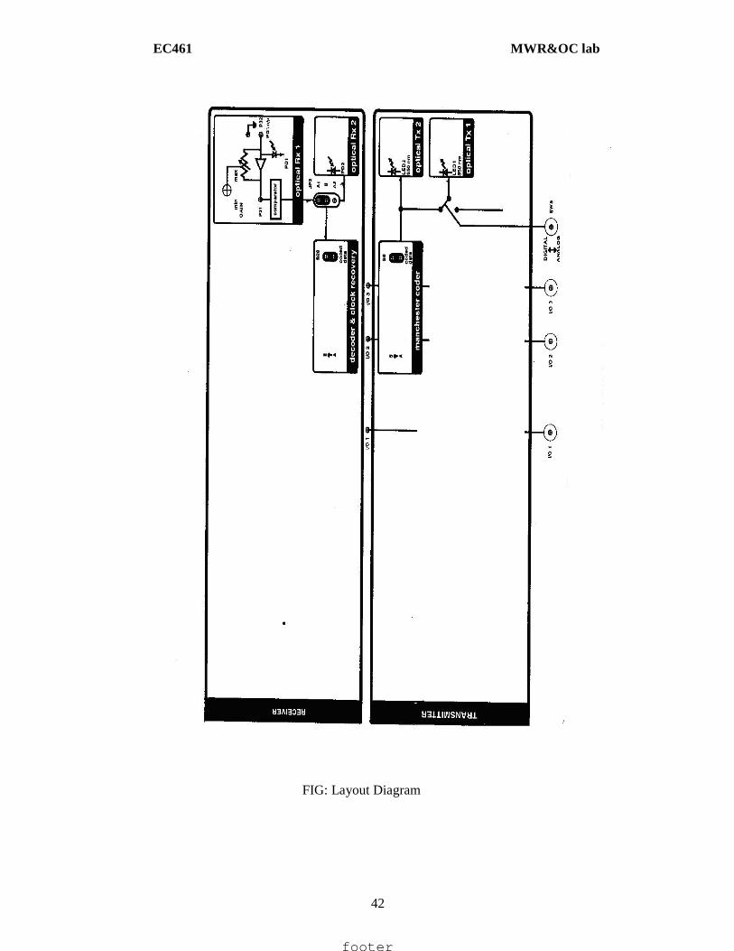
FIG: Layout Diagram
footer
EC461 MWR&OC lab
43
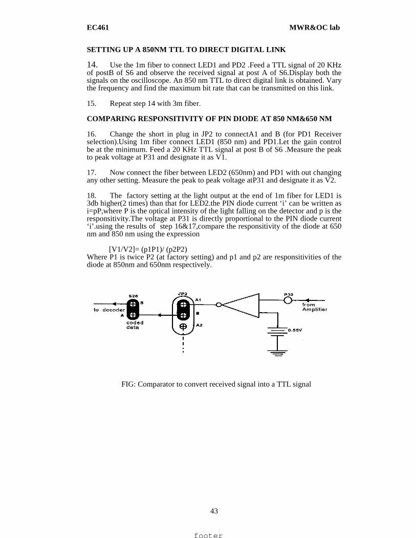
SETTING UP A 850NM TTL TO DIRECT DIGITAL LINK 14. Use the 1m fiber to connect LED1 and PD2 .Feed a TTL signal of 20 KHz of postB of S6 and observe the received signal at post A of S6.Display both the signals on the oscilloscope. An 850 nm TTL to direct digital link is obtained. Vary the frequency and find the maximum bit rate that can be transmitted on this link. 15. Repeat step 14 with 3m fiber. COMPARING RESPONSITIVITY OF PIN DIODE AT 850 NM&650 NM 16. Change the short in plug in JP2 to connectA1 and B (for PD1 Receiver selection).Using 1m fiber connect LED1 (850 nm) and PD1.Let the gain control be at the minimum. Feed a 20 KHz TTL signal at post B of S6 .Measure the peak to peak voltage at P31 and designate it as V1. 17. Now connect the fiber between LED2 (650nm) and PD1 with out changing any other setting. Measure the peak to peak voltage atP31 and designate it as V2. 18. The factory setting at the light output at the end of 1m fiber for LED1 is 3db higher(2 times) than that for LED2.the PIN diode current ‘i’ can be written as i=pP,where P is the optical intensity of the light falling on the detector and p is the responsitivity.The voltage at P31 is directly proportional to the PIN diode current ‘i’.using the results of step 16&17,compare the responsitivity of the diode at 650 nm and 850 nm using the expression
[V1/V2]= (p1P1)/ (p2P2)
Where P1 is twice P2 (at factory setting) and p1 and p2 are responsitivities of the diode at 850nm and 650nm respectively.
FIG: Comparator to convert received signal into a TTL signal
footer
EC461 MWR&OC lab
44
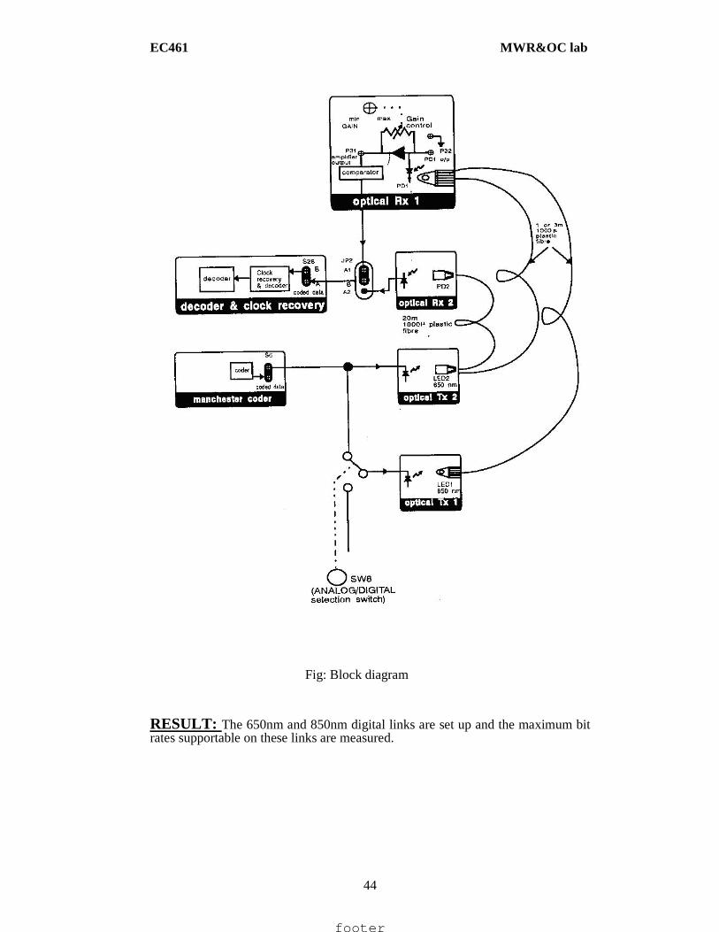
Fig: Block diagram
RESULT: The 650nm and 850nm digital links are set up and the maximum bit rates supportable on these links are measured.
footer
EC461 MWR&OC lab
45
EXPERIMENT 13 SET UP OF TIME DIVISION MULTIPLEXING USING FIBER
OPTICS
AIM : The objective of this experiment is to learn to set up the multiplexer and de-multiplexer and to observe the simultaneous transmission of several channels (two voice and 8 data channels) using Time Division Multiplexing. At the same time, some basic concepts of time switching and asynchronous data interfacing using over sampling are studied. APPARATUS:
1. OFT 2. Two channel 20 MHz Oscilloscope 3. function generator,1Hz-1MHz
THEORY:
OFT is as much a synchronous Time Division Multiplexing unit as it is a fiber optic communication unit. The basic Multiplexer has twelve 64 kbps channels which are time multiplexed. The multiplexed data stream is Manchester coded and the resulting TTL bit-stream drives the LED’s (E/O converters).At the receiver the TTL signal is fed to a Manchester decoder which recovers the clock and the data.
Time Division Multiplexing is also the basis of time- switching used today in telecom services. While multiplexing, say the voice signal from port1,V1 is transmitted before V2, the voice signal from port2.but the receiver ,the first received signal can be fed to port2,and the later signal to port1 ,resulting in switching between the two ports.
If an asynchronous low bit rate signal is to be inserted in a synchronous mux the simplest technique is to sample the input signal using submultiples of mux output clock. How ever this gives rise to jitter in the received signal. This phenomenon is studied in this experiment. PROCEDURE: Set up:
1. The interfaces used in the experiment are summarized in table. The block diagrams of the circuits used in this experiment are shown in fig and for the transmitter and receiver respectively. Set the jumpers and switches and short the shorting links as given in table. The experiment requires the setting up of an 850 nm or 650 nm digital links as discussed in experiment.
footer
EC461 MWR&OC lab
46
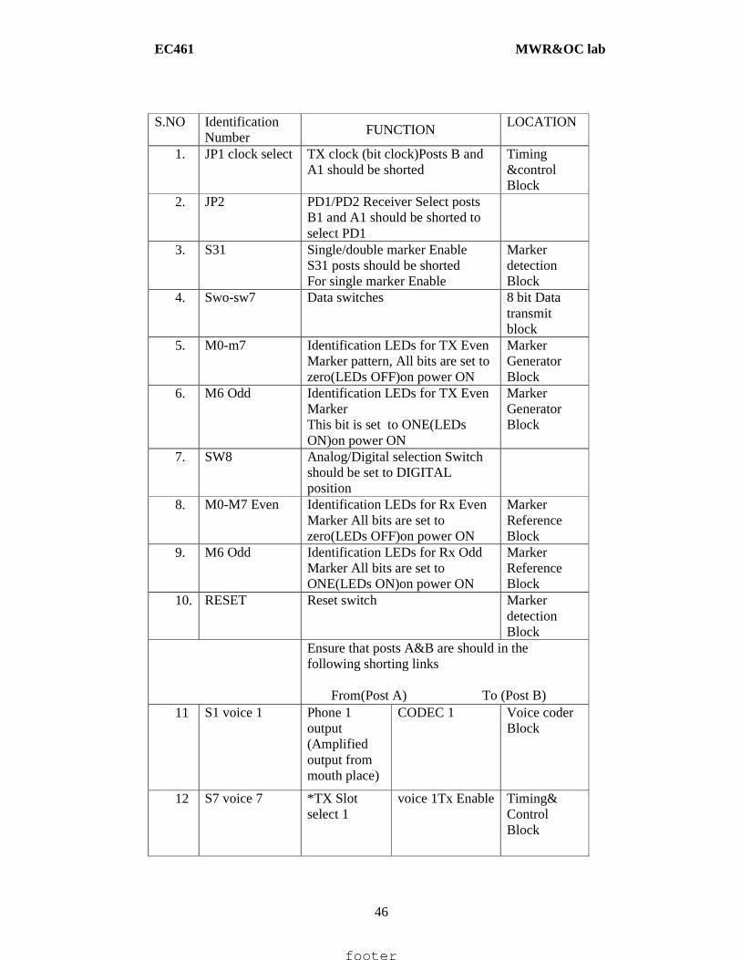
S.NO Identification
Number FUNCTION
LOCATION
1. JP1 clock select TX clock (bit clock)Posts B and A1 should be shorted
Timing &control Block
2. JP2 PD1/PD2 Receiver Select posts B1 and A1 should be shorted to select PD1
3. S31 Single/double marker Enable S31 posts should be shorted For single marker Enable
Marker detection Block
4. Swo-sw7 Data switches 8 bit Data transmit block
5. M0-m7 Identification LEDs for TX Even Marker pattern, All bits are set to zero(LEDs OFF)on power ON
Marker Generator Block
6. M6 Odd Identification LEDs for TX Even Marker This bit is set to ONE(LEDs ON)on power ON
Marker Generator Block
7. SW8 Analog/Digital selection Switch should be set to DIGITAL position
8. M0-M7 Even Identification LEDs for Rx Even Marker All bits are set to zero(LEDs OFF)on power ON
Marker Reference Block
9. M6 Odd Identification LEDs for Rx Odd Marker All bits are set to ONE(LEDs ON)on power ON
Marker Reference Block
10. RESET Reset switch Marker detection Block
Ensure that posts A&B are should in the following shorting links From(Post A) To (Post B)
11 S1 voice 1 Phone 1 output (Amplified output from mouth place)
CODEC 1 Voice coder Block
12 S7 voice 7 *TX Slot select 1
voice 1Tx Enable Timing& Control Block
footer
EC461 MWR&OC lab
47
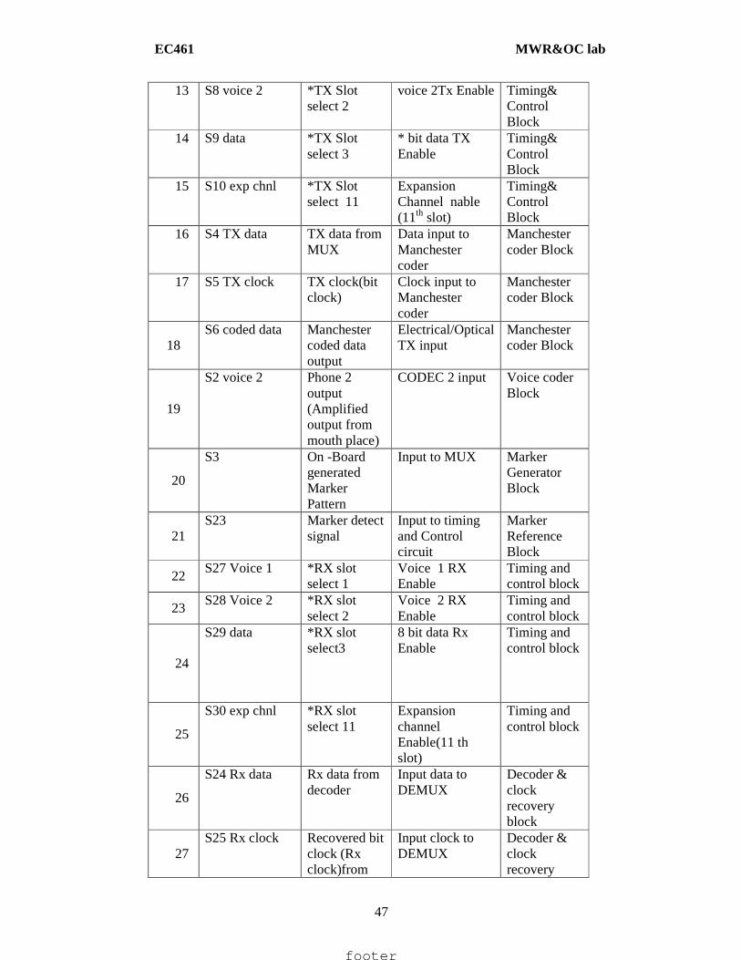
13 S8 voice 2 *TX Slot select 2
voice 2Tx Enable Timing& Control Block
14 S9 data *TX Slot select 3
* bit data TX Enable
Timing& Control Block
15 S10 exp chnl *TX Slot select 11
Expansion Channel nable (11th slot)
Timing& Control Block
16 S4 TX data TX data from MUX
Data input to Manchester coder
Manchester coder Block
17 S5 TX clock TX clock(bit clock)
Clock input to Manchester coder
Manchester coder Block
18 S6 coded data Manchester
coded data output
Electrical/Optical TX input
Manchester coder Block
19
S2 voice 2 Phone 2 output (Amplified output from mouth place)
CODEC 2 input Voice coder Block
20
S3 On -Board generated Marker Pattern
Input to MUX Marker Generator Block
21 S23 Marker detect
signal Input to timing and Control circuit
Marker Reference Block
22 S27 Voice 1 *RX slot
select 1 Voice 1 RX Enable
Timing and control block
23 S28 Voice 2 *RX slot
select 2 Voice 2 RX Enable
Timing and control block
24
S29 data *RX slot select3
8 bit data Rx Enable
Timing and control block
25
S30 exp chnl *RX slot select 11
Expansion channel Enable(11 th slot)
Timing and control block
26
S24 Rx data Rx data from decoder
Input data to DEMUX
Decoder & clock recovery block
27 S25 Rx clock Recovered bit
clock (Rx clock)from
Input clock to DEMUX
Decoder & clock recovery
footer
EC461 MWR&OC lab
48
clock recovery unit
block
28
S26 coded data Out from optical Rx1/Rx2 block
Decoder & clock recovery input
Decoder & clock recovery block
29 LED1 850nm
850 nm LED (Optical Tx1) Optical Tx1 block
30 LED2 650nm
650 nm LED (Optical Tx2) Optical Tx2 block
31 PD2 Optical Receiver with TTL out
put(optical Rx2) Optical Rx2 block
32 PD1 PIN Detector (Optical) Optical Rx1
block
33 GAIN GAIN control Potentiometer Optical Rx1
block
34
P1 TTL in
TTL input at SW7(TxD7)when SW7 is ON
8 bit data transmit block
35
P2 TTL in
TTL input at SW6(TxD6)when SW6 is ON
8 bit data transmit block
36
P5 Signal for Tx&Rx marker programming
8 bit data transmit block
37 P6 Feeding point for TX Even
Marker pattern Programming Marker generator block
38 P7 Feeding point for TX odd
Marker bit Programming Marker generator block
39 P21 TTL out TTL (Rx D7) output 8 bit data
receive block
40 P22 TTL out TTL( Rx D6) output 8 bit data
receive block
41 P23 voice1 CODEC1 output Voice
decoder block
42 P24 Voice2 CODEC2 output Voice
decoder block
43 P26 Feeding point for RxEven Marker
pattern Programming Marker Reference Block
footer
EC461 MWR&OC lab
49
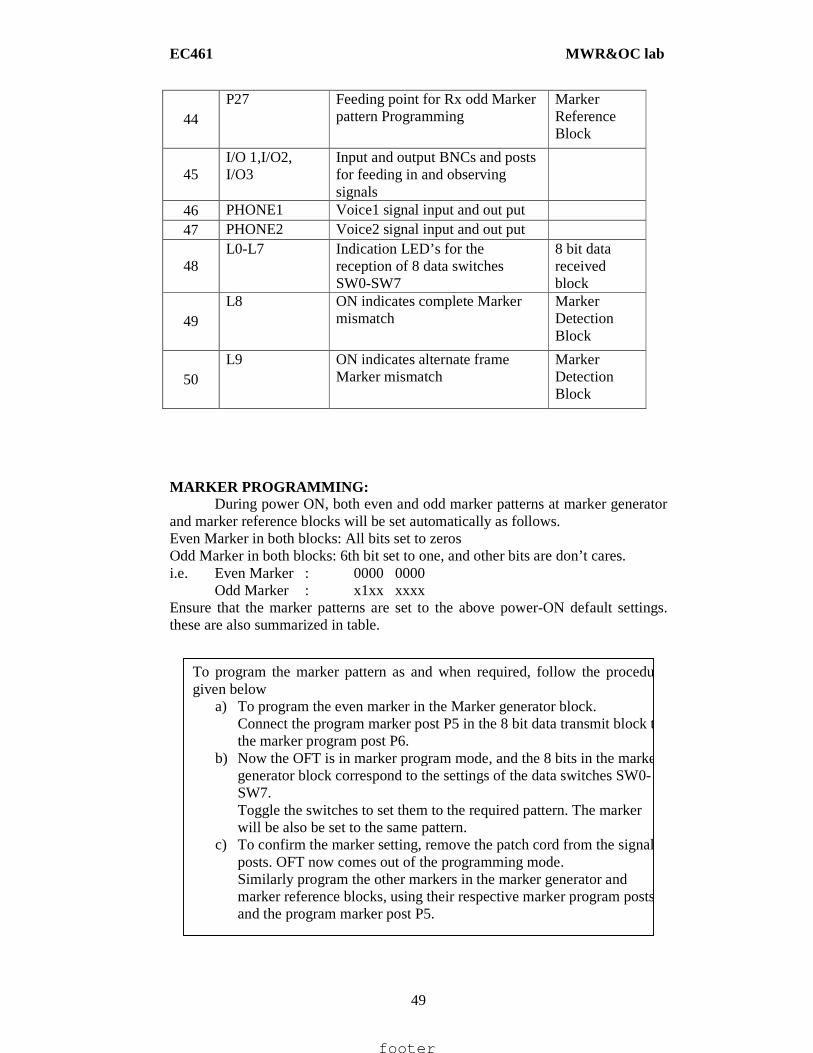
44 P27 Feeding point for Rx odd Marker
pattern Programming Marker Reference Block
45 I/O 1,I/O2, I/O3
Input and output BNCs and posts for feeding in and observing signals
46 PHONE1 Voice1 signal input and out put 47 PHONE2 Voice2 signal input and out put
48 L0-L7 Indication LED’s for the
reception of 8 data switches SW0-SW7
8 bit data received block
49 L8 ON indicates complete Marker
mismatch Marker Detection Block
50 L9 ON indicates alternate frame
Marker mismatch Marker Detection Block
MARKER PROGRAMMING: During power ON, both even and odd marker patterns at marker generator and marker reference blocks will be set automatically as follows. Even Marker in both blocks: All bits set to zeros Odd Marker in both blocks: 6th bit set to one, and other bits are don’t cares. i.e. Even Marker : 0000 0000 Odd Marker : x1xx xxxx Ensure that the marker patterns are set to the above power-ON default settings. these are also summarized in table.
To program the marker pattern as and when required, follow the procedure given below
a) To program the even marker in the Marker generator block. Connect the program marker post P5 in the 8 bit data transmit block to the marker program post P6.
b) Now the OFT is in marker program mode, and the 8 bits in the marker generator block correspond to the settings of the data switches SW0-SW7. Toggle the switches to set them to the required pattern. The marker will be also be set to the same pattern.
c) To confirm the marker setting, remove the patch cord from the signal posts. OFT now comes out of the programming mode. Similarly program the other markers in the marker generator and marker reference blocks, using their respective marker program posts and the program marker post P5.
footer
EC461 MWR&OC lab
50
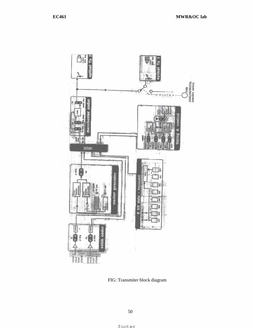
FIG: Transmiter block diagram
footer
EC461 MWR&OC lab
51
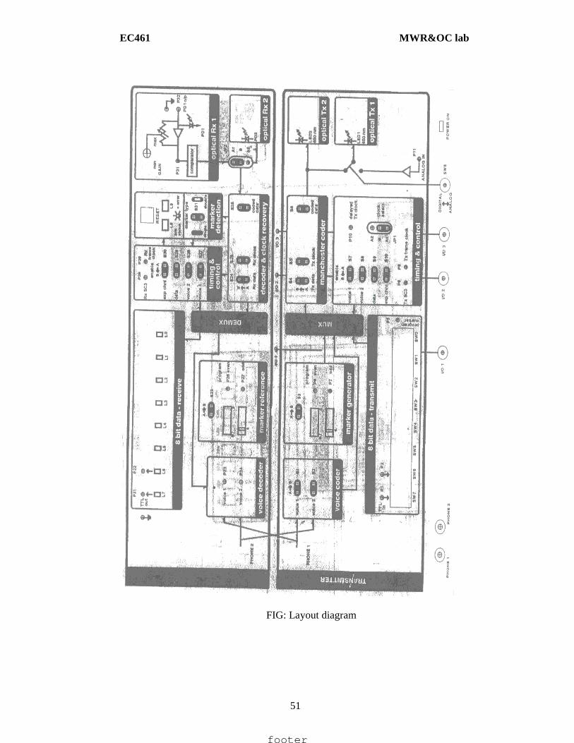
FIG: Layout diagram
footer
EC461 MWR&OC lab
52
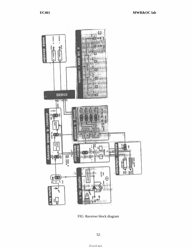
FIG: Receiver block diagram
footer
EC461 MWR&OC lab
53
2. Turn on at least one of the switches SW0-SW7 in the 8 bit data transmit block. This ensures that this multiplexer is correctly aligned, and should be the normal practice when-ever the mux-demux are being used.
3. Connect LED1 in the optical Tx1 block and PD1 in the optical Rx1 block using the 1m optical fiber to set up the 850 nm digital link. Adjust the GAIN control until the LED’s L0-L7 in 8 bit data receiver block light up corresponding to the ON positions of SW0-SW7.when the TDM link is working the LED’s L8 and L9 in the marker detection block will be off with out any flicker. Toggle SWO and observe the toggling of L0.The digital link and the TDM MUX-DEMUX are now set up. Connect the telephone handsets at PHONE 1&PHONE 2. If there is any difficulty in setting up the link, first set up the digital link as described in experiment2.Ensure that the marker pattern settings are as per the power-on settings given in table. Turn the power off and turn it on again to reset the markers in case they are different. Press the reset switch in the marker detection block. The multiplexer demultiplexer should now work.
4. OFT is now being used in the loop-back mode. The data and multiplexed on the transmit side and demultiplexed on the receive side of the trainer. The voice input at the mouth piece is now being looped backed through the fiber to the earpiece. Check this by disturbing the fiber link by removing the fiber from PD1, while speaking into the mouth piece of one of the handsets. Note that you can now no longer hear yourself in the earpiece. .(the best way to check this is to blow into the mouth piece while you disturb the link) TIME SWITCHING OF VOICE :
5. Establish the fiber link again. Remove the shorting plugs of the voice enable shorting links S7 andS8 in the timing and control block on the transmitter side. Using the patch cards, interchange the voice slots by interconnecting the slot Select 1 signal (postA of S7) to the voice enable2 (postB of S8) and the slot select2 signal (post A of S8) to the voice enable1 (postB of S7) at the TX side.voice1 and voice2 are cross connected and the conversation can be carried out between the two people using the two phones. The two slots carrying voice data are now time switched to provide necessary connection. Carry on a conversation, while at the same time turning data switches SW0-SW7 on and off, to observe the simultaneous transmission of 8-bit data in one channel and two voice channels on the link. Reconnect the shorting links S7and S8 to restore the original connection. How ever now remove the shorting plugs of voice enable shorting links S27&S28 in the timing& control block on the receiver side, and cross connect them as explained before. Note that once again the voice1 &voice2 are cross connected. This cross connection is now on the Rx side. Now remove S7&S8 again and cross connect as before. Note that voice 1 TX signal is now connected back to voice1 Rx.switching at both transmitter and receiver cancel out each other.
footer

EC461 MWR&OC lab
54
FIG: Insertion of TTL signals
VOICE BAND WIDTH: 6. Reconnect shorting links S7, S8, S27 and S28.Remove the shorting plug
of voice1 shorting linkS1 in the voice coder block (the phone1 mike is now detached).Feed a sinusoidal signal of 1KHz and 1V p-p with zero DC at postB of S1 and display it on channel 1 of the oscilloscope .Trigger the scope on channel1.Observe the received signal at voice1 signal postP23 on channel2 of the scope. Vary the frequency of the input signal and observe the received signal. Note the lower frequency cutoff and higher frequency cutoff when the out put voltage falls to 0.7V peak to peak (3 db below 1V p-p).
The signal is being digitized by a CODEC at 64 kbps, multiplexed and transmitted on the fiber link. The received optical signal is converted to a TTL signal demultiplexed to obtain the transmitted signal back. The signal at P23 is the reconstructed version of the signal. The frequency response obtained is that of the CODEC used to digitize and reconstruct the voice signal. Observe the received signal closely on the oscilloscope. Note that it is a step approximation of the original signal as shown in fig .can you explain why? ASYNCHRONOUS DATA TRANSMISSION USING OVER SAMPLING :
8. The multiplexer also multiplexes the TTL signals controlled by switches SW0-SW7.
at the receiver, the received signal is demultiplexed and switch inputs are displayed at the LED’s L0-L7 respectively.OFT also provides for directly feeding in two low frequency TTL signals instead of the static switch settings at SW7&SW6.If SW7&SW6 are kept in the ON position, then asynchronous TTL signals from a function generator (the function generator signal is not synchronized to the clock of the multiplexer) can be inserted at P1&P2, as per fig. received signal can then be observed at P21&P22 respectively. RESULT: The simultaneous transmission of several channels (two voice and 8 data channels) using Time Division Multiplexing are observed.
footer
EC461 MWR&OC lab
55
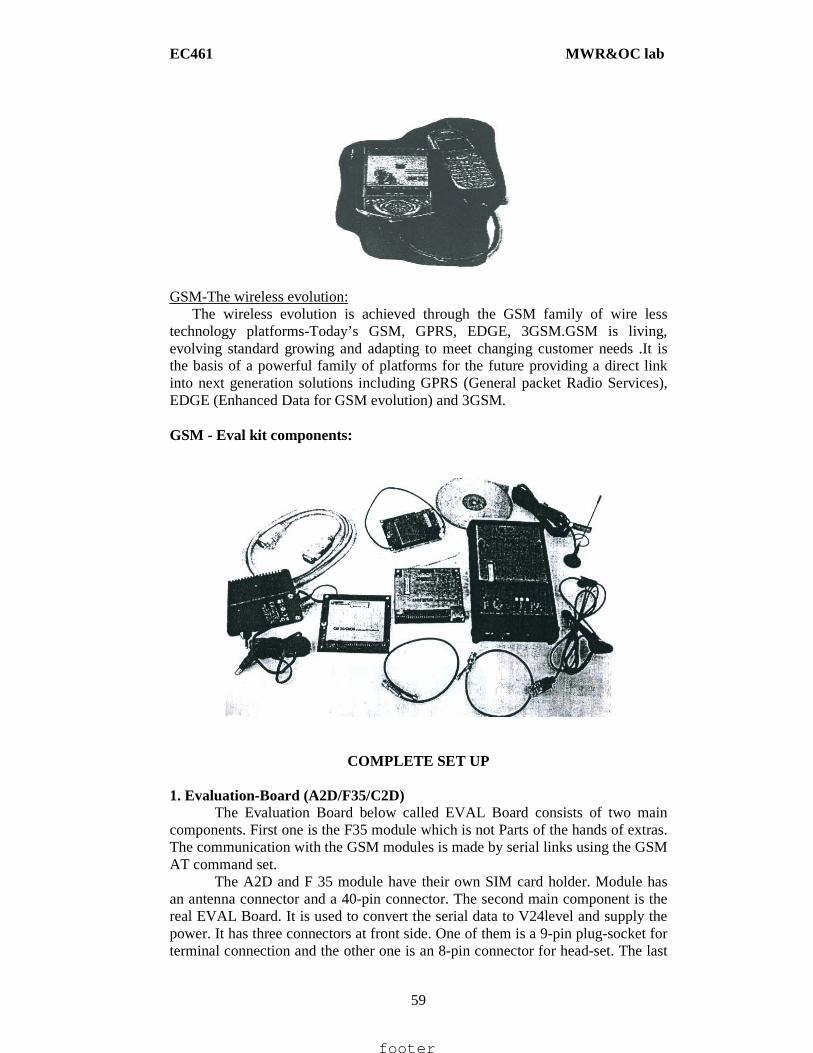
EXPERIMENT 14 STUDY OF CELLULAR COMMUNICATIONS
AIM :
• Understanding theory of GSM technology • Network Architecture • Data services & capability • System up gradation
APPARATUS:
GSM-Eval kit includes following components 1. Evaluation Board (A2D/F35/C2D). 2. F35-A-2:TC35 MODULE with IMEI number. 3. A2D/F35/C2D evaluation board PCB. 4. GSM antenna and cable with coaxial plug(30cm). 5. RS-232 nine pin serial cable. 6. Headset with RJ-45 plug. 7. Wall mount power adapter. 8. A2D-Test software & Hyper Terminal windows s/w. 9. Other extra accessories
THEORY : What is GSM?
The global system for mobile communication (GSM) is an international digital cellular telecommunications standard. The GSM Standard is released by ETSI (European Standard and technology Institute) back in 1989.First commercial services were launched in 1991.After its early introduction on Europe .The standard went global in1992 when GSM services were introduced in Australia .Since then GSM became the most widely adapted and fastest growing digital cellular standard ,and it is positioned to become the world’s dominant cellular standard .In fact ,as of January 1999,GSM accounted for more than 120 million subscribers, according to the GSM Memorandum of Understanding (MoU) Association .With 324GSM networks in operation in 129 countries , GSM provides almost complete coverage around the globe. GSM STANDARDIZATION :
Global System for Mobile (GSM)is a second generation cellular standard that was developed to solve the fragmentation problems of the first cellular systems in Europe.GSM was the world’s first cellular system to specify digital modulation & network level architectures & services and is the world’s most popular 2G technology. Before GSM, European countries used different cellular standard throughout the continent, it was not possible for a customer to use a single subscriber unit throughout Europe. AS of 2001,there were over 350 million GSM subscribers worldwide.
footer
EC461 MWR&OC lab
56
The GSM standard was developed by the Group Special Mobile (SMG) which was an initiative of the conference of European Post and Telecommunications (CEPT) administrations. The underlying aim was to design a uniform pan European mobile System to replace the existing incompatible analog systems. Work on the standard was started in 1982, and the first full set of specifications (phase I) became available in 1990.The responsibility for GSM standardization now resides with SGM under the European Standard and technology Institute (ETSI). GSM SYSTEM ARCHITECTURE: GSM REQUENCIES:
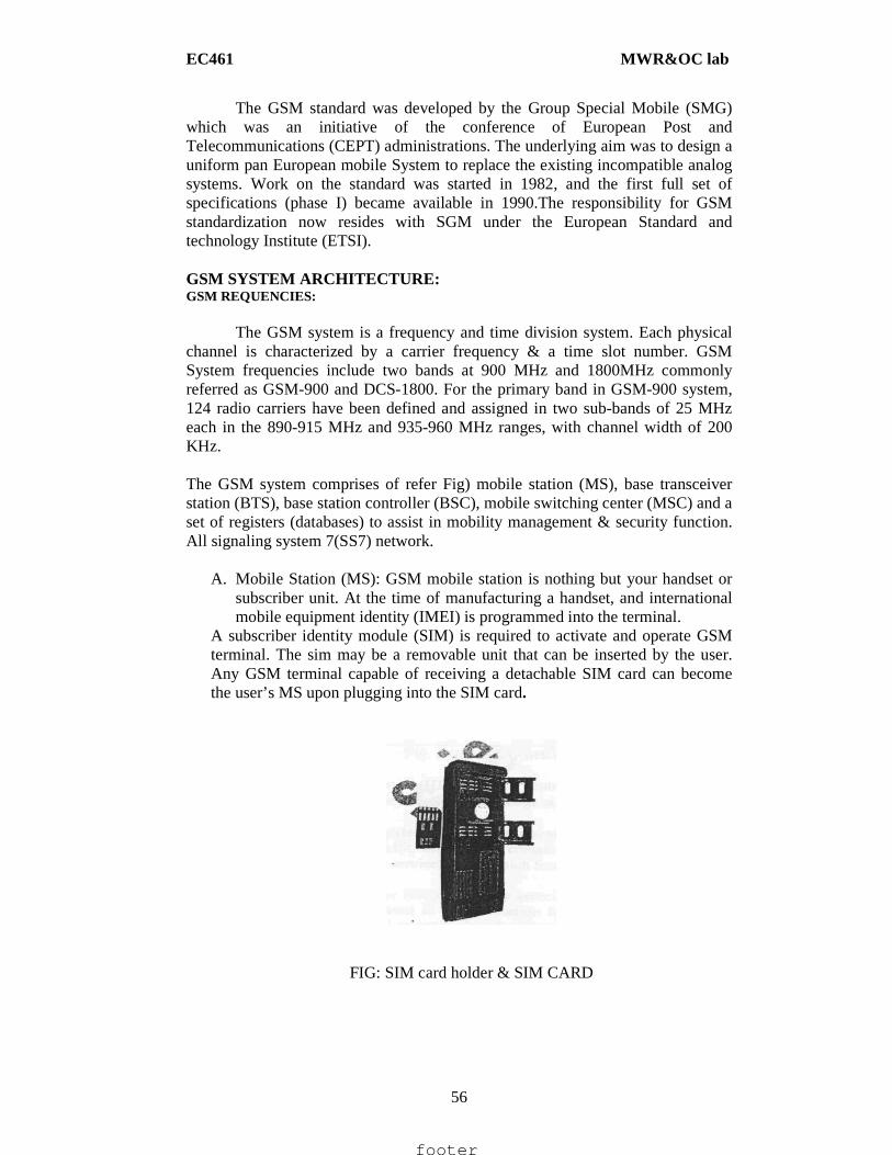
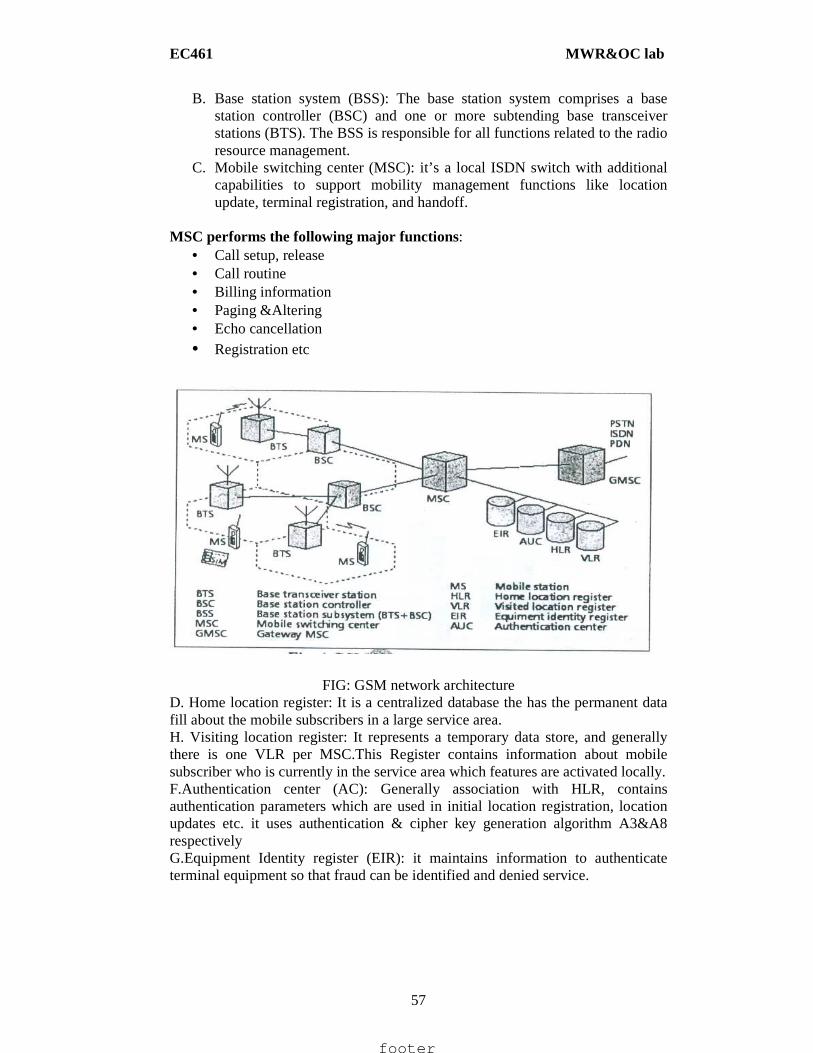
The GSM system is a frequency and time division system. Each physical channel is characterized by a carrier frequency & a time slot number. GSM System frequencies include two bands at 900 MHz and 1800MHz commonly referred as GSM-900 and DCS-1800. For the primary band in GSM-900 system, 124 radio carriers have been defined and assigned in two sub-bands of 25 MHz each in the 890-915 MHz and 935-960 MHz ranges, with channel width of 200 KHz. The GSM system comprises of refer Fig) mobile station (MS), base transceiver station (BTS), base station controller (BSC), mobile switching center (MSC) and a set of registers (databases) to assist in mobility management & security function. All signaling system 7(SS7) network.
A. Mobile Station (MS): GSM mobile station is nothing but your handset or subscriber unit. At the time of manufacturing a handset, and international mobile equipment identity (IMEI) is programmed into the terminal.
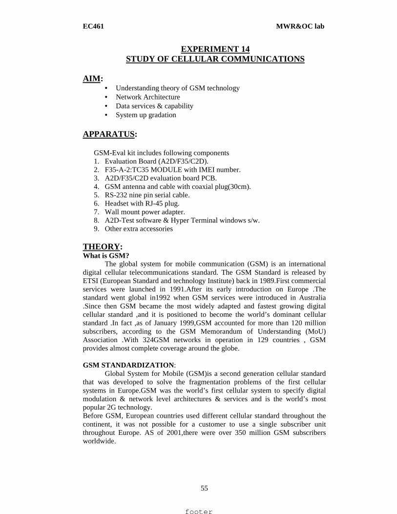
A subscriber identity module (SIM) is required to activate and operate GSM terminal. The sim may be a removable unit that can be inserted by the user. Any GSM terminal capable of receiving a detachable SIM card can become the user’s MS upon plugging into the SIM card.
FIG: SIM card holder & SIM CARD
footer
EC461 MWR&OC lab
57
B. Base station system (BSS): The base station system comprises a base station controller (BSC) and one or more subtending base transceiver stations (BTS). The BSS is responsible for all functions related to the radio resource management.
C. Mobile switching center (MSC): it’s a local ISDN switch with additional capabilities to support mobility management functions like location update, terminal registration, and handoff.
MSC performs the following major functions:
• Call setup, release • Call routine • Billing information • Paging &Altering • Echo cancellation • Registration etc
FIG: GSM network architecture D. Home location register: It is a centralized database the has the permanent data fill about the mobile subscribers in a large service area. H. Visiting location register: It represents a temporary data store, and generally there is one VLR per MSC.This Register contains information about mobile subscriber who is currently in the service area which features are activated locally. F.Authentication center (AC): Generally association with HLR, contains authentication parameters which are used in initial location registration, location updates etc. it uses authentication & cipher key generation algorithm A3&A8 respectively G.Equipment Identity register (EIR): it maintains information to authenticate terminal equipment so that fraud can be identified and denied service.
footer
EC461 MWR&OC lab
58
GSM CAPABILITY & DATA SERVICES : Characteristics of the initial GSM standard include the following
� Fully digital system utilizing the 900MHZ frequency band. � TDMA over radio carrier (200 KHz carrier spacing) � User/terminal authentication for fraud control � Full international roaming capability � Compatibility with ISDN for supplementary services � Support of short message services(SMS)
GSM supports a range of basic and supplementary services like bearer
services, teleservices and supplementary services. The common ISDN like supplementary services supported by GSM include the following.
• Call forwarding • Call barring • Call waiting • Call hold • Call charge etc. Call forwarding & barring are defined in the original GSM specification
(phase 1). GSM data services consist of circuit-switched and packet-switched data. Circuit switched data can be to an analog modem, to an ISDN connection, or to a fax machine. Packet switched data connects to a packet network.
The GSM GPRS extends the packet capabilities of GSM to higher data rates and longer messages. The service supports sending point to point and point to multipoint messages. Two nodes are addressed to the GSM network to support GPRS.
footer
EC461 MWR&OC lab
59
GSM-The wireless evolution:
The wireless evolution is achieved through the GSM family of wire less technology platforms-Today’s GSM, GPRS, EDGE, 3GSM.GSM is living, evolving standard growing and adapting to meet changing customer needs .It is the basis of a powerful family of platforms for the future providing a direct link into next generation solutions including GPRS (General packet Radio Services), EDGE (Enhanced Data for GSM evolution) and 3GSM. GSM - Eval kit components:
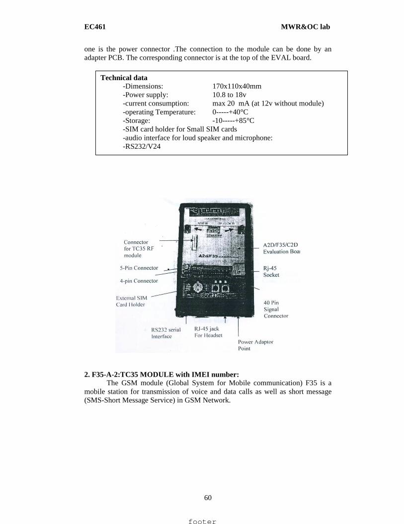
COMPLETE SET UP 1. Evaluation-Board (A2D/F35/C2D)
The Evaluation Board below called EVAL Board consists of two main components. First one is the F35 module which is not Parts of the hands of extras. The communication with the GSM modules is made by serial links using the GSM AT command set.
The A2D and F 35 module have their own SIM card holder. Module has an antenna connector and a 40-pin connector. The second main component is the real EVAL Board. It is used to convert the serial data to V24level and supply the power. It has three connectors at front side. One of them is a 9-pin plug-socket for terminal connection and the other one is an 8-pin connector for head-set. The last
footer
EC461 MWR&OC lab
60
one is the power connector .The connection to the module can be done by an adapter PCB. The corresponding connector is at the top of the EVAL board.
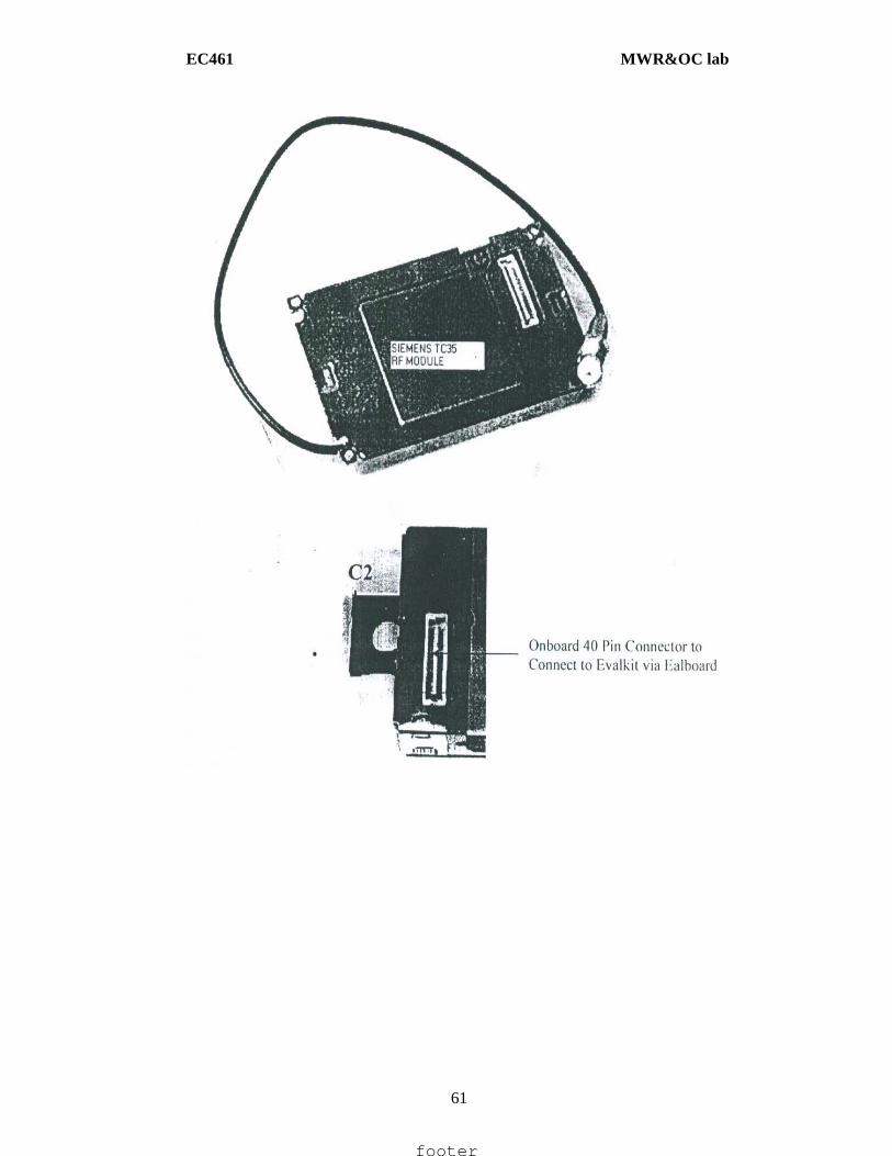
2. F35-A-2:TC35 MODULE with IMEI number:
The GSM module (Global System for Mobile communication) F35 is a mobile station for transmission of voice and data calls as well as short message (SMS-Short Message Service) in GSM Network.
Technical data -Dimensions: 170x110x40mm -Power supply: 10.8 to 18v -current consumption: max 20 mA (at 12v without module) -operating Temperature: 0-----+40°C -Storage: -10-----+85°C -SIM card holder for Small SIM cards -audio interface for loud speaker and microphone: -RS232/V24
footer
EC461 MWR&OC lab
61
footer
EC461 MWR&OC lab
62
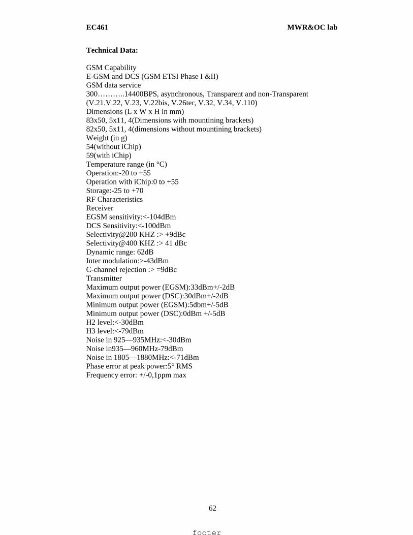
Technical Data: GSM Capability E-GSM and DCS (GSM ETSI Phase I &II) GSM data service 300………..14400BPS, asynchronous, Transparent and non-Transparent (V.21.V.22, V.23, V.22bis, V.26ter, V.32, V.34, V.110) Dimensions (L x W x H in mm) 83x50, 5x11, 4(Dimensions with mountining brackets) 82x50, 5x11, 4(dimensions without mountining brackets) Weight (in g) 54(without iChip) 59(with iChip) Temperature range (in °C) Operation:-20 to +55 Operation with iChip:0 to +55 Storage:-25 to +70 RF Characteristics Receiver EGSM sensitivity:<-104dBm DCS Sensitivity:<-100dBm Selectivity@200 KHZ :> +9dBc Selectivity@400 KHZ :> 41 dBc Dynamic range: 62dB Inter modulation:>-43dBm C-channel rejection :> =9dBc Transmitter Maximum output power (EGSM):33dBm+/-2dB Maximum output power (DSC):30dBm+/-2dB Minimum output power (EGSM):5dbm+/-5dB Minimum output power (DSC):0dBm +/-5dB H2 level:<-30dBm H3 level:<-79dBm Noise in 925—935MHz:<-30dBm Noise in935—960MHz-79dBm Noise in 1805—1880MHz:<-71dBm Phase error at peak power:5° RMS Frequency error: +/-0,1ppm max
footer
EC461 MWR&OC lab
63
4. GSM antenna and cable with coaxial plug(30cm) Operating frequency: 900/1800MHz.
Your modem is actually a low power radio transmitter and receiver. It sends out and receives radio frequency energy .When you use your modem ,the cellular system handling your calls controls both the radio frequency and the power level of your cellular modem.
footer
EC461 MWR&OC lab
64
5. RS232 9 pin serial cable
efault transfer Parameters � Tranfer rate 9600 bps � Echo ON � 8 bit non Parity,1 stop bit
6. Head set with RJ-45 plug
Specifications of RJ45
1. VCC 12 DC 2. RXD (optional) 3. TXD (optional) 4. GND 5. Speaker OUT+ 6. Speaker out- 7. Microphone IN+ 8. Microphone IN
7. Wall mount power adapter
footer
EC461 MWR&OC lab
65
3. RF ENVIRONMENT
PROCEDURE: Step 1: Place Evalboard on a table.
Connect the serial cable to the 9-people COM1 Port of the PC (depending which COM is available) then connect the other end of the serial cable. To the 9-pin SUB-D connector of the EVAL-Board.
Step 2: Remove two screws from the Evalboard.
Pick up an A2D/F35/C2D Evaluation board. Observe it carefully. On left most bottom corner, there is a four pin connector named as BTMP A2D f35. Short rightmost two pins i.e A2D & F35 by jumper (Short Circuit Bridge).
Above this four pin connector, there is another five pin connector. Short pin 3 & 4 from right i.e A2D & BAT. Back side of this board has 40 pins connector (female) socket. Fix it on male 40 pin connector socket available on Evalboard. Proper care should be taken while fixing. All the jumpers should come at bottom side but just above External SIM holder & reset switch. Setp 3: Now take Siemens TC35 module. Fix it on A2D/F35/C2D.Evaluation
board carefully in a similar manner. Caution: do not play with RP module, do not press. Setp 4: How to fix SIM card.
For fixing SIM card, user has two options. Either user can use onboard. Internal SIM holder available on TC35 module or external on Evalkit.
External: Her SIM card fits into the SIM card holder under the plastic. Cover which should be closed by TWISTING the metal flap to “LOCK”.
footer
EC461 MWR&OC lab
66
Internal : On board sim holder is available on tc35 module. BY pressing small push button (c2) take out the holder outside & fixed any working SIM card in it ant fixed. It ant fixed it again in TC35 module. Step5: take GSM 900/1800 MGH antenna. TC35(F35) module has antenna connector and and then lock it properly . Place connected antenna either on top of rack im lab or best way to place it out side of lab in open space environment to get better single strength. Antenna has magnet at bottom side for fixed. Don’ touch antenna while evalkit is on. During experiment, switch of the module & then change antenna position for getting good signal strength & again power on the module. Step 6: for connecting RJ-45plug, user has two positions available. One socket is on evalboard & other is on A2d/F35 board. Choose any one. For example, fixed RJ-45 plug on headphone and mice to EVOL-Board near serial port Step 7: Software interface. Now we can communicate with the module through any terminal program such as Hyper Terminal under Windows. We recommend to use the “A2D-Testsoftware” which is available on the enclosed CD 4.COMMAND LEVEL STUDY :
To control the GSM module there is an advanced set of AT commands according to GSM ETSI (European Telecommunications Standards Institute) 07.07 and 07.05 implemented.
These commands are available in the GSM TRAINER CD-ROM. Open CD-ROM. Go to “manuals” & open “a2dman.pdf”. For that user should have Adobe acrobat reader above 4.0 version. If not available, user can install it from CD-ROM provided. This “a2dman.pdf” document is the set of all ETSI AT commands with GSM 07.05 and 07.07 commands. User should follow this PDF in a sequential order to learn, to understand & to get response from GSM Evalkit with respect to these AT commands. Real Time study of GSM 07.05 & 07.07 AT Commands
a) Command concerning modem & simcard hardware. b) Network registration commands. c) Call control commands d) Call setting commands. e) Call information commands. f) Phone Book commands. g) Serial link control commands.
footer
EC461 MWR&OC lab
67
h) Message setting commands. i) Storing/restoring commands. j) Error message handling &survey & many more………………..
For user reference, some basic as well as important AT commands response is given. INTRODUCTION:
This manual is focused on the GSM data solutions of the FALCOM A2D series from FALCOM GmbH. It contains information about the FALCOM A2D embedded GSM module and the FALCOM A2D-1 GSM modem and phone. It does not contain special information about the GSM related accessories as there are dial-handset, the hands free set, the external battery pack and the mobile data terminals, which are also sold by FALCOM.
Information furnished herein by FALCOM GmbH is believed to be accurate and reliable. However, no responsibility is assumed for its use. Also the information contained herein is subject to change without notice. Users are advised to quickly proceed to the “Security” chapter and read the hints carefully.
Used abbreviations:
ETSI European Telecommunication Standards Institute GSM Global System for Mobile communications IMEI International Mobile station Equipment identity ME Mobile Equipment PLMN Public Land mobile Network PIN Personal identification Number PUK Personal Unblocking Key RP Receive Protocol RXQUAL Received Signal Quality SIM Subscriber identity Module SMS Short Message Service SMS/PP Short Message Service/Point-to-Point TA Terminal Adapter TE Terminal Equipment TP Transmit Protocol
Related documents:
• ETSI GSM 07.05 “Use of Data Terminal Equipment-Data Circuit
Terminating Equipment interface for Short Message Service and Cell Broadcast Service”
• ETSI GSM 07.0 “AT command set for GSM Mobile Equipment”
• ITU-TV.25ter “Serial asynchronous automatic dialing and control”
footer
EC461 MWR&OC lab
68
SECURITY:
IMPORTANT FOR THE EFFICIENT AND SAGE OPERATION OF YOUR GSM MODEM READ THIS INFORMATION BEFORE USE
Your GSM modem is one of the most exciting and innovative electronic products ever developed. With it you can stay in contact with your office, your home, emergency services, and others, wherever service is provided.
GENERAL:
Your modem utilizes the GSM standard for cellular technology. GSM is a newer radio frequency (<<RF>>) technology than the current FM technology that has been used for radio communications for decades. The GSM standard has been established for use in the European community and elsewhere.
Your modem is actually a low power radio transmitter and receiver. It sends out and receives radio frequency energy. When you use your modem the cellular system handling your calls controls both the radio frequency and the power level of your cellular modem.
ESPOSURE TO RF ENERGY:
There has been some public concern about possible health effects of using GSM modem. Although research on health effects from RF energy has focused for many years on the current RF technology, scientists have begun research had been reviewed, and after compliance to all applicable safety standards had been tested, it has been concluded that the product is fit for use.
If you are concerned about exposure to RF energy there are things you can do to minimize exposure. Obviously, limiting the duration of your calls will reduce your exposure to RF energy. In addition, you can reduce RF exposure by operating your cellular modem efficiently by following the below guidelines. EFFICIENT MODEM OPERATION: For your modem to operate at the lowest power level, consistent with satisfactory call quality: If your modem has an extendible antenna, extend it fully. Some models allow you to place a call with the antenna retracted. However your modem operates more efficiently with the antenna fully extended.
Do not hold the antenna when the modem is <<IN USE>>. Holding the antenna affects calls quality and may cause the modem to operate at a higher power level than needed.
footer
EC461 MWR&OC lab
69
ΑΝΤΕΝΝΑ ΑΝΤΕΝΝΑ ΑΝΤΕΝΝΑ ΑΝΤΕΝΝΑ CARE AND REPLACEMENT : Do not use the modern with a damaged antenna. If a damaged antenna comes into contact with the skin, a minor bur may result. Replace a damaged antenna immediately. Consult your manual to see if you may change the antenna yourself. If so, use only a manufacturer-approved antenna. Otherwise, have your antenna repaired by a qualified technician. Use only the supplied or approved antenna. Un-authorized antennas, modifications or attachments, modifications or attachments could damage the modern and may contravene local RF emission regulations or invalidate type approval. DRIVING : Check the laws and regulations on the use of cellular devices in the area where you drive. Always obey them. Also, when using your modem while driving, please : give full attention to driving, pull off the road and park before making of answering a call if driving conditions so require. When applications are prepared for mobile use they should fulfill road-safety instructions of the current law! ΕΕΕΕLECTRONIC DEVICES: Most electronic equipment, for example in hospitals and motor vehicles is shielded from RF energy. However RF energy may affect some malfunctioning or improperly shielded electronic equipment. VEHICLE ELECTRONIC EQUIPMENT: Check your vehicle manufacturer’s representative to determine if any on board electronic equipment is adequately shielded from RF energy. MEDICAL ELECTRONIC EQUIPMENT: Consult the manufacturer of any personal medical devices (such as pacemakers, hearing aids, etc…..) to determine if they are adequately shielded from external RF energy. Turn your modem OFF in health care facilities when any regulations posted in the area instruct you to do so. Hospitals or health care facilities may be using RF monitoring equipment. AIRCRAFT: Turn your modem OFF before boarding any aircraft. Use it on the ground only with crew permission. Do not use in the air. To prevent possible interference with aircraft systems, Federal Aviation Administration (FAA) regulations require you to have permission from a crew member to use your modem while the plane is on the ground. To prevent interference with cellular systems, local RF regulations prohibit using your modem whilst airborne.
CHILDREN: Do not allow children to play with your modern. It is not a toy. Children could hurt themselves or others (by poking themselves or others in the eye with the antenna, for example).children could damage the modem, or make calls that increase your modem bills. BLASTING AREAS TO avoid interfering with blasting operations, turn your unit OFF when in a<<blasting area>>or in areas posted:<turn off two-way radio>>.construction crew often use remote control RF devices to set off explosives.
footer

EC461 MWR&OC lab
70
POTENTIALLY EXPLOSIVE ATMOSPHERES Turn your modem OFF when in any area with a potentially explosive atmosphere. It is rare, but your modem or its accessories could generate sparks. Sparks in such areas could cause an explosion or fire resulting in bodily injury or even death. Areas with a potentially explosive atmosphere are often, but not always, clearly marked. They include fuelling areas such as petrol stations; below decks on boats; fuel or chemical transfer or storage facilities; and areas where the air contains chemicals or particles. Such as grain, dust, or metal powders. Do not transport or store flammable gas, liquid, or explosives, in the compartment of your vehicle which contains your modem or accessories .Before using your modem in a vehicle powered by liquefied petroleum gas (such as propane or butane) ensure that the vehicle complies with the relevant fire and safety regulations of the country in which the vehicle is to be used. NON-IONISING RADIATION As with other mobile radio transmitting equipment, users are advised that for satisfactory operation and for the safety of personnel, it is recommended that no part of the human body be allowed to come too close to the antenna during operation of the equipment. The radio equipment shall be connected to the antenna via a non-radiating 50ohm coaxial cable. The antenna shall be mounted in such a position that no part of the human body will normally rest close to any part of the antenna. It is also recommended to use the equipment not close to medical devices as for example hearing aids and pacemakers. SAFETY STANDARDS THIS CELLULAR MODEM COMPLIES WITH ALL APPLICABLE RF SAFETY STANDARDS .
COMMANDS : HARDWARE COMMANDS:
1. AT+CGMI 2. AT+CGMM 3. AT+CGMR 4. AT+CGSN 5. AT+CIMI 6. AT+CCID
NETWORK REGISTRATION COMMANDS
1. AT+CPIN 2. AT+CREG 3. AT+COPS 4. AT+CSQ 5. AT+CCED
footer
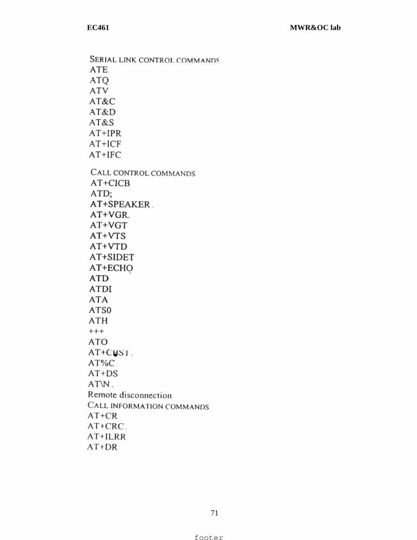
EC461 MWR&OC lab
71
footer
Related Documents