Uw logo Opportunities for HALT/HASS in designing robust electronics Isabelle Vervenne Flanders’ Mechatronics Engineering Centre Katholieke Hogeschool Brugge-Oostende

Welcome message from author
This document is posted to help you gain knowledge. Please leave a comment to let me know what you think about it! Share it to your friends and learn new things together.
Transcript
Uw logo
Opportunities for HALT/HASS in designing robust electronics
Isabelle Vervenne
Flanders’ Mechatronics Engineering CentreKatholieke Hogeschool Brugge-Oostende

Uw logo
Outline
• Introduction
• HALT
• HASS/HASA

Uw logo 3
Predominant failure causes

Uw logo
Environmental Stress Screening
• Goal: remove the “weak” ones out of the whole population
• Method:– Start with an identical population
– Increase the temperature and vibration stress
• Other method:– HASS

Uw logo
Objective of HALT
• Highly Accelerated Life Testing
• Objective:find weak links in design and fabrication processes of a product during design phase
• �DVT: Design Verification Testing – Tests done before product release

Uw logo
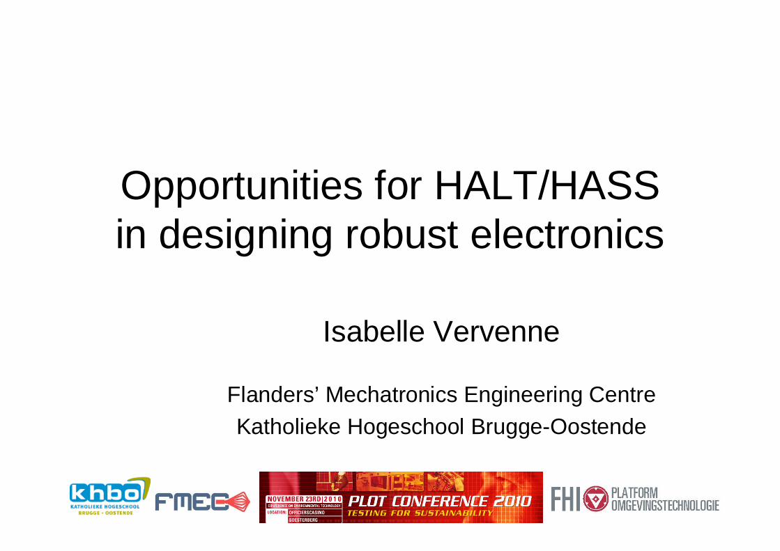
HALT: what is it?
• Process of discovery and optimization– Operating limits and destruct limits: points where the
system ceases to work as specified but will return to operation if the stress is removed (operating limit) and ceases to operate even if the stress is removed (destruct limit)
– Try to maximize the operating and destruct margins of the product
• Not a pass/fail test
Uw logo
HALT: what is it?
• Product is stressed well outside operating specifications– Stress until “fundamental limits of technology”
• Stimulate failures (not simulate the environment)
• Find failures - fix “on the fly” and continue testing
Uw logo
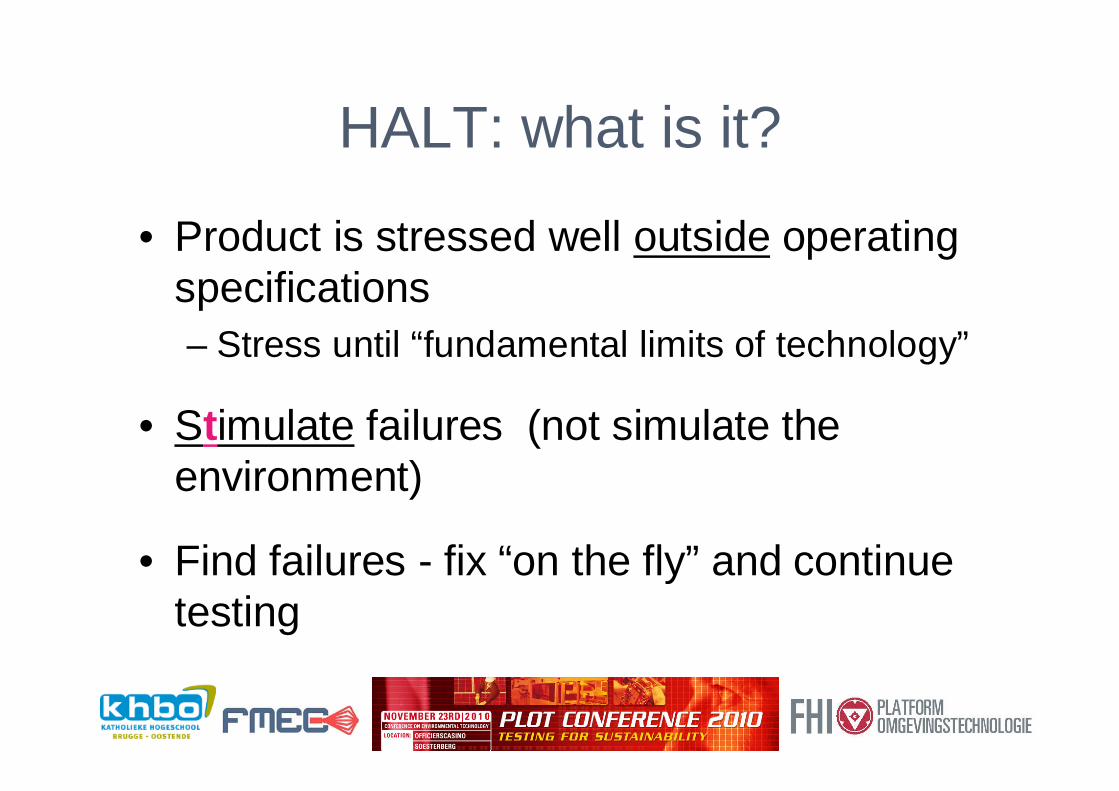
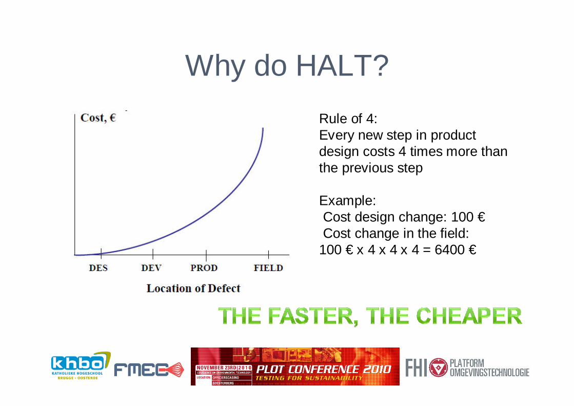
Why do HALT?
Uw logo
Why do HALT?
Rule of 4:Every new step in product design costs 4 times more than the previous step
Example:Cost design change: 100 €Cost change in the field:
100 € x 4 x 4 x 4 = 6400 €
Uw logo
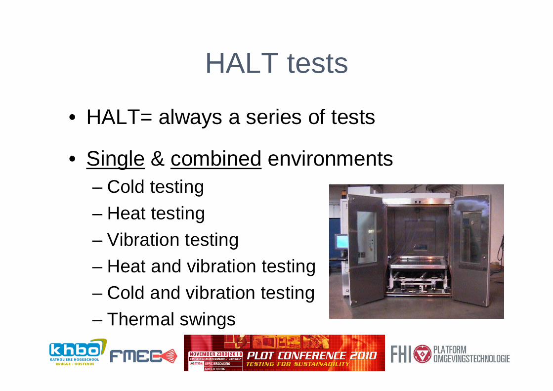
HALT tests
• HALT= always a series of tests
• Single & combined environments– Cold testing
– Heat testing
– Vibration testing
– Heat and vibration testing
– Cold and vibration testing
– Thermal swings
Uw logo
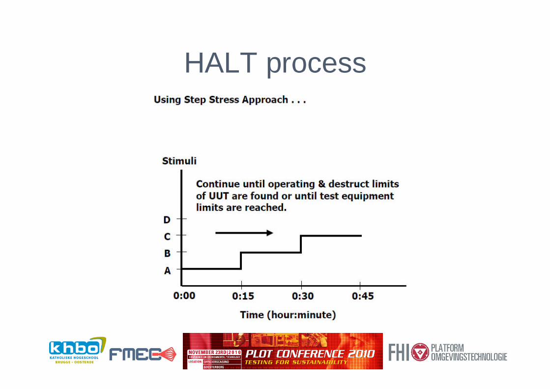
HALT process

Uw logo
HALT test results
Uw logo
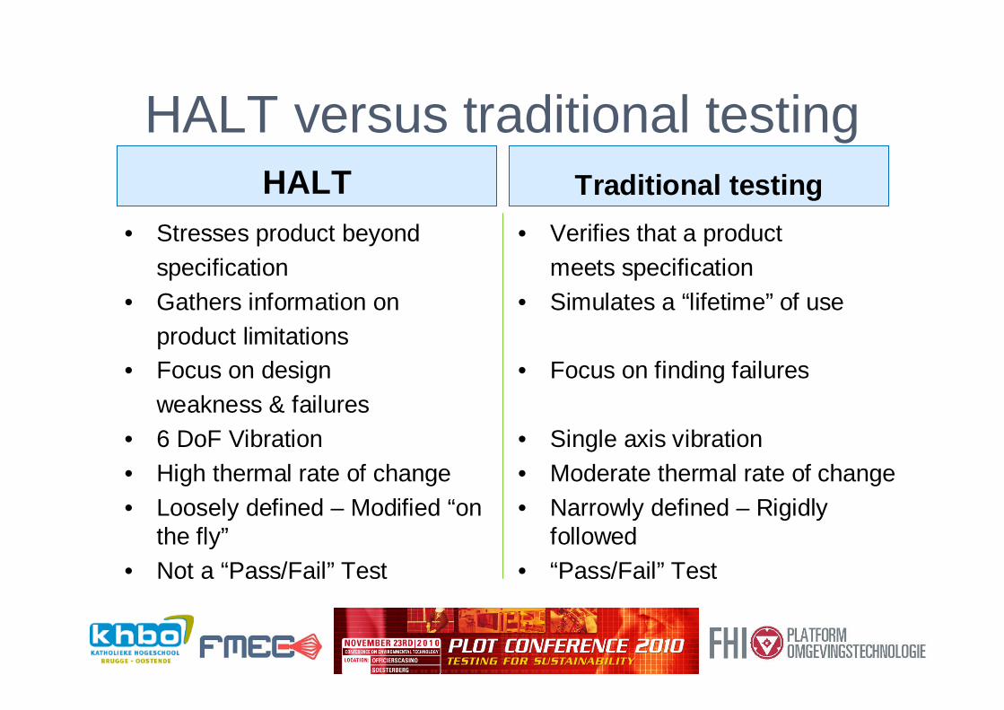
HALT versus traditional testingHALT
• Stresses product beyondspecification
• Gathers information onproduct limitations
• Focus on designweakness & failures
• 6 DoF Vibration• High thermal rate of change• Loosely defined – Modified “on
the fly”• Not a “Pass/Fail” Test
Traditional testing
• Verifies that a productmeets specification
• Simulates a “lifetime” of use
• Focus on finding failures
• Single axis vibration• Moderate thermal rate of change• Narrowly defined – Rigidly
followed• “Pass/Fail” Test

Uw logo
HALT benefits
• Quickly discover design & process limitations
• Evaluate & improve design margins
• Characterize statistical information on margins
• Faster time to market
• Increased reliability �more robust products
• Greater customer satisfaction
• Lowered warranty cost through higher MTBF
• Minimized chance of product recalls
Uw logo
When is HALT not indicated?
• HALT is not recommended or cost effective for extremely low production rates products
• HALT is not recommended for one of a kind or very expensive products
• HALT does not replace qualification testing such as that performed for spaceapplications
Uw logo
HASS/HASA
• Highly accelerated stress screen/audit
• Less extreme version of HALT-test on sub-assembly or final assembly level
• Performed on all production units or on a statistical relevant amount of units
• Precipitate latent defects/workmanship defects and correct

Uw logo
Benefits of HASS/HASA• Detect & correct design & process changes• Reduce production time and cost• Increase out-of-box quality and field reliability• Decrease field service and warranty costs• Reduce infant mortality rate at product
introductionHASS is not a test, it’s a process
Each product has its own process
Uw logo
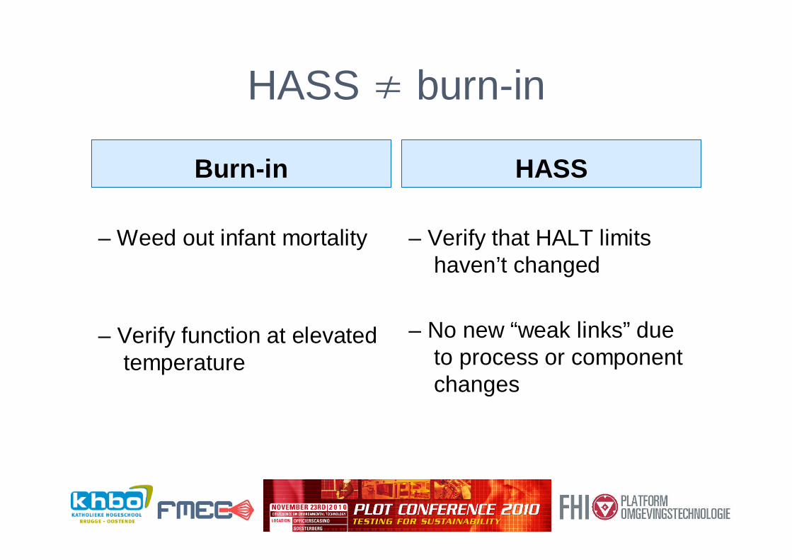
HASS ≠ burn-in
Burn -in
– Weed out infant mortality
– Verify function at elevated temperature
HASS
– Verify that HALT limits haven’t changed
– No new “weak links” due to process or component changes

Uw logo
HASS screen diagram
Uw logo
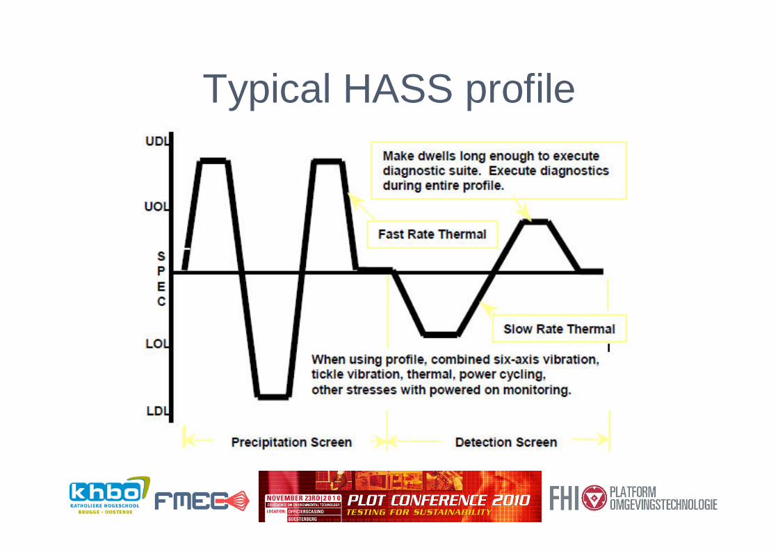
Typical HASS profile
Uw logo
Proof-of-screen
• Serves two key purposes:– Verify that the screen is not taking excessive life out of the product
– Verify that the screen is effectively finding defective units
Uw logo
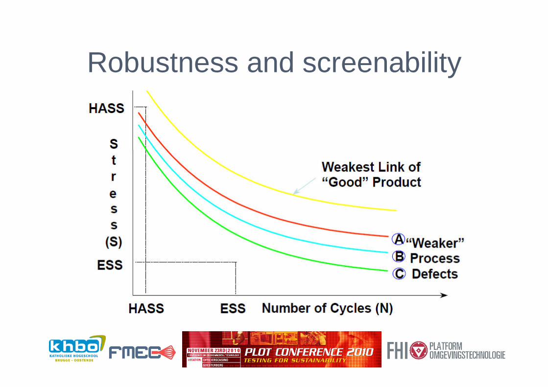
Robustness and screenability
Uw logo
Typical defects detected in HASS
• IC process changes
• Solder issues
• Electrical tolerance
• Component placement
• Mechanical tolerance
• IC process problems
• Timing problems
• Raw board problems
Uw logo
When is HASS not indicated?
• HASS is not needed if a product is mature and the vendors and manufacturing process cannot be changed
• HASA can be used for high production products to provide nearly the same protection as 100% HASS screening

Uw logo
HASS versus ESS
Current Stress Screening
HASS
Screening coverage 100% (on every unit) 100% (on every unit)
Screening time/unit 36h 4h
Lifetime reduction Unknown Less than 3%
Stress nature Temperature and vibration separatedLow thermal transition rates
Temperature and multi-axis vibration combinedHigh thermal transition rates
Fixture (mounting) Only for vibration Dedicated to have uniform temperature and vibration stress
When to use For all quantities Not for very low quantities
Uw logo
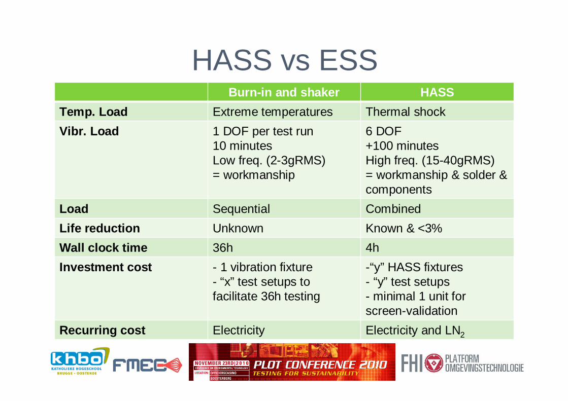
HASS vs ESSBurn-in and shaker HASS
Temp. Load Extreme temperatures Thermal shock
Vibr. Load 1 DOF per test run10 minutesLow freq. (2-3gRMS)= workmanship
6 DOF+100 minutesHigh freq. (15-40gRMS)= workmanship & solder & components
Load Sequential Combined
Life reduction Unknown Known & <3%
Wall clock time 36h 4h
Investment cost - 1 vibration fixture- “x” test setups to facilitate 36h testing
-“y” HASS fixtures- “y” test setups- minimal 1 unit for screen-validation
Recurring cost Electricity Electricity and LN2
Related Documents