16 Operational Amplifiers and Active Filters: A Bond Graph Approach Gilberto González and Roberto Tapia University of Michoacan Mexico 1. Introduction The most important single linear integrated circuit is the operational amplifier. Operational amplifiers (op-amp) are available as inexpensive circuit modules, and they are capable of performing a wide variety of linear and nonlinear signal processing functions (Stanley, 1994). In simple cases, where the interest is the configuration gain, the ideal op-amp in linear circuits, is used. However, the frequency response and transient response of operational amplifiers using a dynamic model can be obtained. The bond graph methodology is a way to get an op-amp model with important parameters to know the performance. A bond graph is an abstract representation of a system where a collection of components interact with each other through energy ports and are place in the system where energy is exchanged (Karnopp & Rosenberg, 1975). Bond graph modelling is largely employed nowadays, and new techniques for structural analysis, model reduction as well as a certain number of software packages using bond graph have been developed. In (Gawthrop & Lorcan, 1996) an ideal operational amplifier model using the bond graph technique has been given. This model only considers the open loop voltage gain and show an application of active bonds. In (Gawthrop & Palmer, 2003), the `virtual earth' concept has a natural bicausal bond graph interpretation, leading to simplified and intuitive models of systems containing active analogue electronic circuits. However, this approach does not take account the type of the op-amp to consider their internal parameters. In this work, a bond graph model of an op-amp to obtain the time and frequency responses is proposed. The input and output resistances, the open loop voltage gain, the slew rate and the supply voltages of the operational amplifier are the internal parameters of the proposed bond graph model. In the develop of this work, the Bond Graph model in an Integral causality assignment (BGI) to determine the properties of the state variables of a system is used (Wellstead, 1979; Sueur & Dauphin-Tanguy, 1991). Also, the symbolic determination of the steady state of the variables of a system based on the Bond Graph model in a Derivative causality assignment (BGD) is applied (Gonzalez et al., 2005). Finally, the simulations of the systems represented Source: New Approaches in Automation and Robotics, Book edited by: Harald Aschemann, ISBN 978-3-902613-26-4, pp. 392, May 2008, I-Tech Education and Publishing, Vienna, Austria Open Access Database www.intehweb.com www.intechopen.com

Welcome message from author
This document is posted to help you gain knowledge. Please leave a comment to let me know what you think about it! Share it to your friends and learn new things together.
Transcript
16
Operational Amplifiers and Active Filters: A Bond Graph Approach
Gilberto González and Roberto Tapia University of Michoacan
Mexico
1. Introduction
The most important single linear integrated circuit is the operational amplifier. Operational amplifiers (op-amp) are available as inexpensive circuit modules, and they are capable of performing a wide variety of linear and nonlinear signal processing functions (Stanley, 1994). In simple cases, where the interest is the configuration gain, the ideal op-amp in linear circuits, is used. However, the frequency response and transient response of operational amplifiers using a dynamic model can be obtained. The bond graph methodology is a way to get an op-amp model with important parameters to know the performance. A bond graph is an abstract representation of a system where a collection of components interact with each other through energy ports and are place in the system where energy is exchanged (Karnopp & Rosenberg, 1975). Bond graph modelling is largely employed nowadays, and new techniques for structural analysis, model reduction as well as a certain number of software packages using bond graph have been developed. In (Gawthrop & Lorcan, 1996) an ideal operational amplifier model using the bond graph technique has been given. This model only considers the open loop voltage gain and show an application of active bonds. In (Gawthrop & Palmer, 2003), the `virtual earth' concept has a natural bicausal bond graph interpretation, leading to simplified and intuitive models of systems containing active analogue electronic circuits. However, this approach does not take account the type of the op-amp to consider their internal parameters. In this work, a bond graph model of an op-amp to obtain the time and frequency responses is proposed. The input and output resistances, the open loop voltage gain, the slew rate and the supply voltages of the operational amplifier are the internal parameters of the proposed bond graph model. In the develop of this work, the Bond Graph model in an Integral causality assignment (BGI) to determine the properties of the state variables of a system is used (Wellstead, 1979; Sueur & Dauphin-Tanguy, 1991). Also, the symbolic determination of the steady state of the variables of a system based on the Bond Graph model in a Derivative causality assignment (BGD) is applied (Gonzalez et al., 2005). Finally, the simulations of the systems represented
Source: New Approaches in Automation and Robotics, Book edited by: Harald Aschemann, ISBN 978-3-902613-26-4, pp. 392, May 2008, I-Tech Education and Publishing, Vienna, Austria
Ope
n A
cces
s D
atab
ase
ww
w.in
tehw
eb.c
om
www.intechopen.com
New Approaches in Automation and Robotics
284
by bond graph models using the software 20-Sim by Controllab Products are realized (Controllab Products, 2007). Therefore, the main result of this work is to present a bond graph model of an op-amp considering the internal parameters of a type of linear integrated circuit and external elements connected to the op-amp, for example, the feedback circuit and the load. The outline of the paper is as follows. Section 2 and 3 summarizes the background of bond graph modelling with an integral and derivative causality assignment. Section 4 the bond graph model of an operational amplifier is proposed. Also, the frequency responses of the some linear integrated circuits that represent operational amplifier using the proposed bond graph model are obtained. Section 5 gives a comparator circuit using a bond graph model and obtaining the time response. Section 6 presents the proposed bond graph model of an feedback op-amp; the input and output resistances, bandwidth, slew rate and supply voltages of a non-inverting amplifier using BGI and BGD are determined. Section 7 gives the filters using a bond graph model of an op-amp. In this section, we apply the filters for a complex signal in the physical domain. The bond graph model of an op-amp to design a Proportional and Integral (PI) controller and to control the velocity of a DC motor in a closed loop system is applied in section 8. Finally, the conclusions are given in section 9.
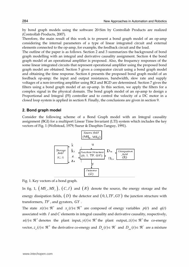
2. Bond graph model
Consider the following scheme of a Bond Graph model with an Integral causality assignment (BGI) for a multiport Linear Time Invariant (LTI) system which includes the key vectors of Fig. 1 (Wellstead, 1979; Sueur & Dauphin-Tanguy, 1991).
Fig. 1. Key vectors of a bond graph.
In fig. 1, ( ),e f
MS MS , ( ),C I and ( )R denote the source, the energy storage and the
energy dissipation fields, ( )D the detector and ( )0,1, ,TF GY the junction structure with
transformers, TF , and gyrators, GY .
The state ( )∈ℜnx t and ( )∈ℜm
dx t are composed of energy variables ( )p t and ( )q t
associated with I andC elements in integral causality and derivative causality, respectively,
( )∈ℜ pu t denotes the plant input, ( )∈ℜq
y t the plant output, ( )∈ℜnz t the co-energy
vector, ( )∈ℜm
dz t the derivative co-energy and ( )∈ℜr
inD t and ( )∈ℜr
outD t are a mixture
www.intechopen.com
Operational Amplifiers and Active Filters: A Bond Graph Approach
285
of ( )e t and ( )f t showing the energy exchanges between the dissipation field and the
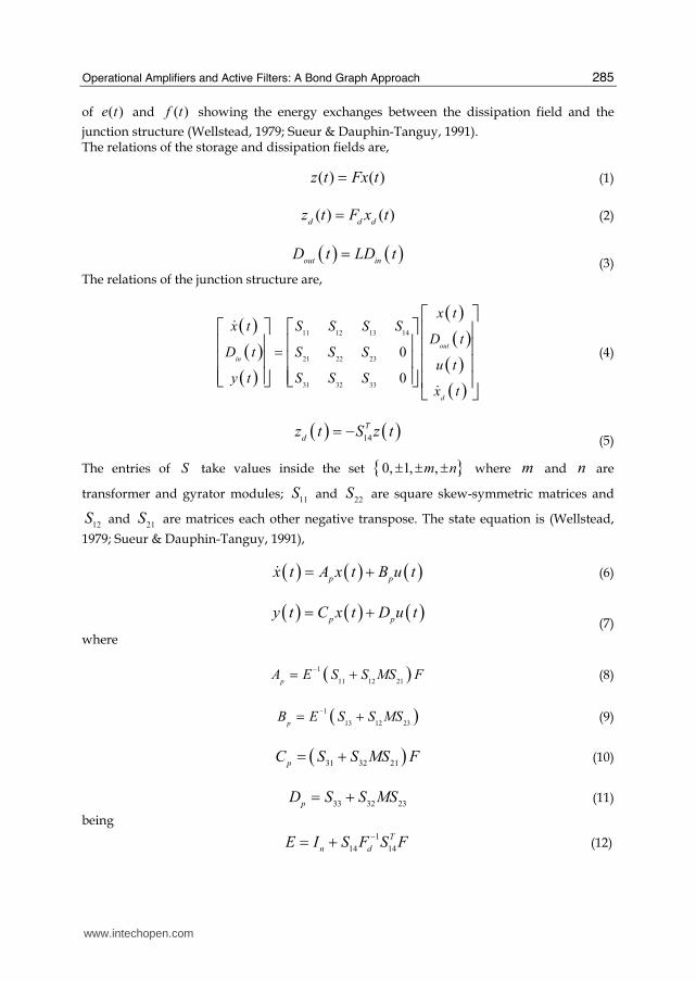
junction structure (Wellstead, 1979; Sueur & Dauphin-Tanguy, 1991). The relations of the storage and dissipation fields are,
( ) ( )=z t Fx t (1)
( ) ( )=d d dz t F x t (2)
( ) ( )=
out inD t LD t
(3) The relations of the junction structure are,
( )( )( )
( )( )( )( )
11 12 13 14
21 22 23
31 32 33
0
0
=⎡ ⎤⎡ ⎤ ⎡ ⎤ ⎢ ⎥⎢ ⎥ ⎢ ⎥ ⎢ ⎥⎢ ⎥ ⎢ ⎥ ⎢ ⎥⎢ ⎥ ⎢ ⎥⎣ ⎦ ⎣ ⎦ ⎢ ⎥⎣ ⎦
&
&
out
in
d
x tx t S S S S
D tD t S S S
u ty t S S S
x t
(4)
( ) ( )14
= − T
dz t S z t
(5)
The entries of S take values inside the set { }0, 1, ,± ± ±m n where m and n are
transformer and gyrator modules; 11S and
22S are square skew-symmetric matrices and
12S and
21S are matrices each other negative transpose. The state equation is (Wellstead,
1979; Sueur & Dauphin-Tanguy, 1991),
( ) ( ) ( )= +&p p
x t A x t B u t (6)
( ) ( ) ( )= +
p py t C x t D u t
(7) where
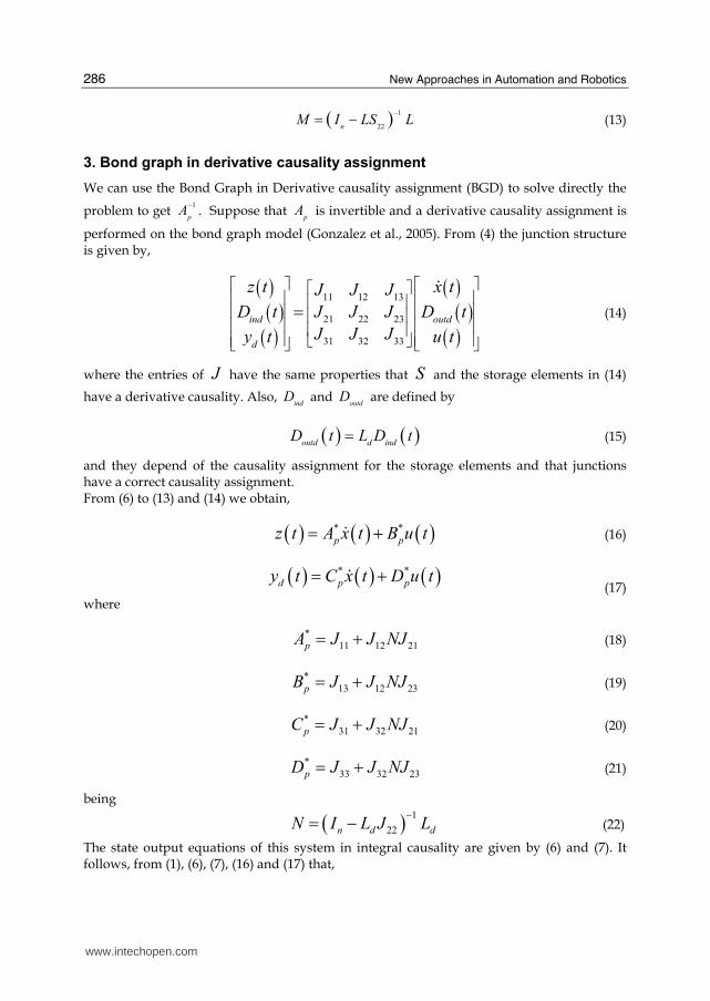
( )1
11 12 21
−= +pA E S S MS F (8)
( )1
13 12 23
−= +pB E S S MS (9)
( )31 32 21= +
pC S S MS F (10)
33 32 23
= +pD S S MS (11)
being
1
14 14
−= + T
n dE I S F S F (12)
www.intechopen.com
New Approaches in Automation and Robotics
286
( ) 1
22
−= −n
M I LS L (13)
3. Bond graph in derivative causality assignment
We can use the Bond Graph in Derivative causality assignment (BGD) to solve directly the
problem to get 1−pA . Suppose that
pA is invertible and a derivative causality assignment is
performed on the bond graph model (Gonzalez et al., 2005). From (4) the junction structure is given by,
( )( )( )( )( )( )
11 12 13
21 22 23
31 32 33
⎡ ⎤ ⎡ ⎤⎡ ⎤⎢ ⎥ ⎢ ⎥⎢ ⎥⎢ ⎥ ⎢ ⎥⎢ ⎥⎢ ⎥ ⎢ ⎥⎢ ⎥⎢ ⎥ ⎢ ⎥⎣ ⎦⎣ ⎦ ⎣ ⎦=
&
ind outd
d
z t x tJ J J
D t J J J D t
J J Jy t u t
(14)
where the entries of J have the same properties that S and the storage elements in (14)
have a derivative causality. Also, indD and
outdD are defined by
( ) ( )=outd d indD t L D t (15)
and they depend of the causality assignment for the storage elements and that junctions have a correct causality assignment. From (6) to (13) and (14) we obtain,
( ) ( ) ( )* *
p pz t A x t B u t= +& (16)
( ) ( ) ( )* *
d p py t C x t D u t= +& (17)
where
*
11 12 21pA J J NJ= + (18)
*
13 12 23pB J J NJ= + (19)
*
31 32 21pC J J NJ= + (20)
*
33 32 23pD J J NJ= + (21)
being
( ) 1
22n d dN I L J L−= − (22)
The state output equations of this system in integral causality are given by (6) and (7). It follows, from (1), (6), (7), (16) and (17) that,
www.intechopen.com
Operational Amplifiers and Active Filters: A Bond Graph Approach
287
* 1
p pA FA−= (23)
* 1
p p pB FA B−= − (24)
* 1
p p pC C A−= (25)
* 1
p p p p pD D C A B−= − (26)
Considering ( ) 0x t =& , the steady state of a LTI MIMO system defined by
1
ss p p ssx A B u−= − (27)
( )1
ss p p p p ssy D C A B u−= − (28)
where ssx and ssy are the steady state of the state variables and the output, respectively.
In an approach of the BGD, the steady state is determined by
1 *
ss p ssx F B u−= (29)
*
ss p ssy D u= (30)
4. A bond graph model of an operational amplifier
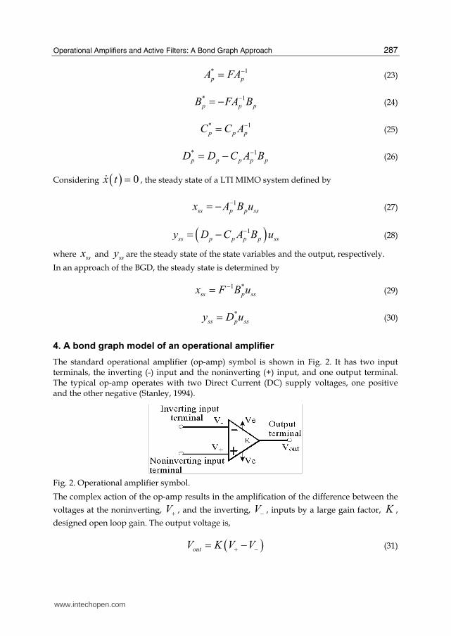
The standard operational amplifier (op-amp) symbol is shown in Fig. 2. It has two input terminals, the inverting (-) input and the noninverting (+) input, and one output terminal. The typical op-amp operates with two Direct Current (DC) supply voltages, one positive and the other negative (Stanley, 1994).
Fig. 2. Operational amplifier symbol.
The complex action of the op-amp results in the amplification of the difference between the
voltages at the noninverting, V+ , and the inverting, V− , inputs by a large gain factor, K ,
designed open loop gain. The output voltage is,
( )outV K V V+ −= − (31)
www.intechopen.com
New Approaches in Automation and Robotics
288
The assumptions of the ideal op-amp are (Barna & Porat, 1989): 1) The input impedance is infinite. 2) The output impedance is zero. 3) The open loop gain is infinite. 4) Infinite bandwidth so that any frequency signal from 0 to ∞ Hz can be amplified without attenuation. 5) Infinite slew rate so that output voltage charges simultaneously with input voltage charges. The implications of the assumptions are: no current will flow either into or out of either input terminal of the op-amp, also, the voltage at the output terminal does not charge as the
loading is varied and finally, from 3H , + −− = outV
V VK
, if we take the limit when K→∞, note
that V V+ −= , which indicates that the voltages at the two input terminals are forced to be
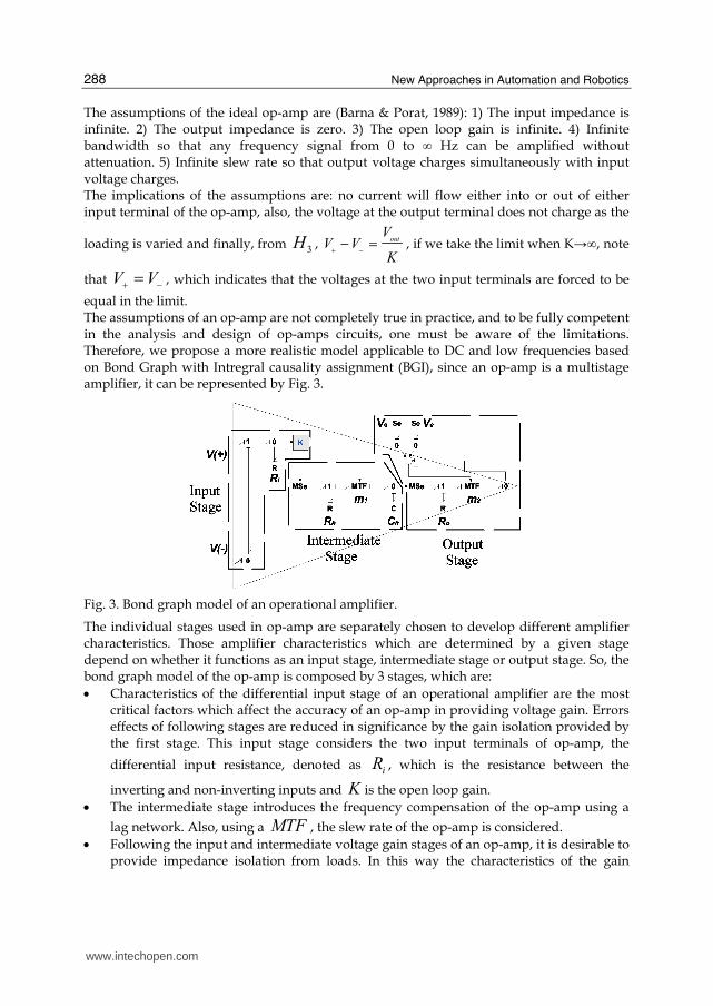
equal in the limit. The assumptions of an op-amp are not completely true in practice, and to be fully competent in the analysis and design of op-amps circuits, one must be aware of the limitations. Therefore, we propose a more realistic model applicable to DC and low frequencies based on Bond Graph with Intregral causality assignment (BGI), since an op-amp is a multistage amplifier, it can be represented by Fig. 3.
Fig. 3. Bond graph model of an operational amplifier.
The individual stages used in op-amp are separately chosen to develop different amplifier characteristics. Those amplifier characteristics which are determined by a given stage depend on whether it functions as an input stage, intermediate stage or output stage. So, the bond graph model of the op-amp is composed by 3 stages, which are:
• Characteristics of the differential input stage of an operational amplifier are the most critical factors which affect the accuracy of an op-amp in providing voltage gain. Errors effects of following stages are reduced in significance by the gain isolation provided by the first stage. This input stage considers the two input terminals of op-amp, the
differential input resistance, denoted as iR , which is the resistance between the
inverting and non-inverting inputs and K is the open loop gain.
• The intermediate stage introduces the frequency compensation of the op-amp using a
lag network. Also, using a MTF , the slew rate of the op-amp is considered.
• Following the input and intermediate voltage gain stages of an op-amp, it is desirable to provide impedance isolation from loads. In this way the characteristics of the gain
www.intechopen.com
Operational Amplifiers and Active Filters: A Bond Graph Approach
289
stages are preserved under load, and adequate signal current is made available to the load. In addition, the output stage provides isolation to the preceding stage and a low output impedance to the load. This stage is formed by the output terminal, the output
resistance of the op-amp denoted as oR and the adjustment of supply voltages, positive
voltage cV and negative voltage eV , are applied using a MTF element.
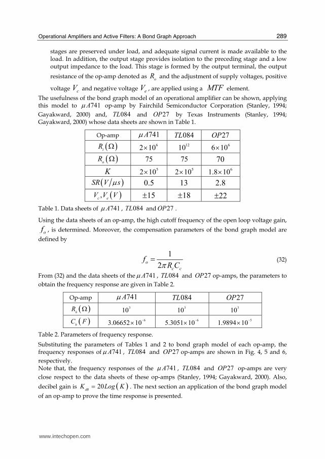
The usefulness of the bond graph model of an operational amplifier can be shown, applying this model to 741μA op-amp by Fairchild Semiconductor Corporation (Stanley, 1994;
Gayakward, 2000) and, 084TL and 27OP by Texas Instruments (Stanley, 1994; Gayakward, 2000) whose data sheets are shown in Table 1.
Op-amp 741μA 084TL 27OP ( )ΩiR 6
2 10× 12
10 6
6 10× ( )ΩoR 75 75 70
K 5
2 10× 5
2 10× 6
1.8 10× ( )μSR V s 0.5 13 2.8 ( ),c eV V V 15± 18± 22±
Table 1. Data sheets of 741μA , 084TL and 27OP .
Using the data sheets of an op-amp, the high cutoff frequency of the open loop voltage gain,
of , is determined. Moreover, the compensation parameters of the bond graph model are
defined by
1
2o
c c
fR Cπ= (32)
From (32) and the data sheets of the 741μA , 084TL and 27OP op-amps, the parameters to
obtain the frequency response are given in Table 2.
Op-amp 741μA 084TL 27OP ( )ΩhR 3
10 3
10 3
10
( )hC F 6
3.06652 10−×
65.3051 10
−× 5
1.9894 10−×
Table 2. Parameters of frequency response.
Substituting the parameters of Tables 1 and 2 to bond graph model of each op-amp, the frequency responses of 741μA , 084TL and 27OP op-amps are shown in Fig. 4, 5 and 6,
respectively. Note that, the frequency responses of the 741μA , 084TL and 27OP op-amps are very
close respect to the data sheets of these op-amps (Stanley, 1994; Gayakward, 2000). Also,
decibel gain is ( )20=dBK Log K . The next section an application of the bond graph model
of an op-amp to prove the time response is presented.
www.intechopen.com

New Approaches in Automation and Robotics
290
Fig. 4. Frequency response of 741μA op-amp.
Fig. 5. Frequency response of 084TL op-amp.
Fig. 6. Frequency response of 27OP op-amp.
5. Comparator circuit
Comparator circuits represent to the first class of circuits we have considered that are
basically nonlinear in operation. Specifically, comparator circuits produce two or more
discrete outputs, each of which is dependent on the input level (Floyd & Buchla, 1999). In
this application, the op-amp is used in the open loop configuration with the input voltage on
one input and a reference voltage on the other, which is shown in Fig. 7.
www.intechopen.com
Operational Amplifiers and Active Filters: A Bond Graph Approach
291
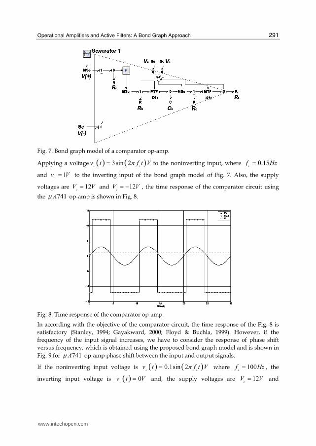
Fig. 7. Bond graph model of a comparator op-amp.
Applying a voltage ( ) ( )3sin 2π+ +=v t f t V to the noninverting input, where 0.15+ =f Hz
and 1− =v V to the inverting input of the bond graph model of Fig. 7. Also, the supply
voltages are 12=cV V and 12= −
eV V , the time response of the comparator circuit using
the 741μA op-amp is shown in Fig. 8.
Fig. 8. Time response of the comparator op-amp.
In according with the objective of the comparator circuit, the time response of the Fig. 8 is
satisfactory (Stanley, 1994; Gayakward, 2000; Floyd & Buchla, 1999). However, if the
frequency of the input signal increases, we have to consider the response of phase shift
versus frequency, which is obtained using the proposed bond graph model and is shown in
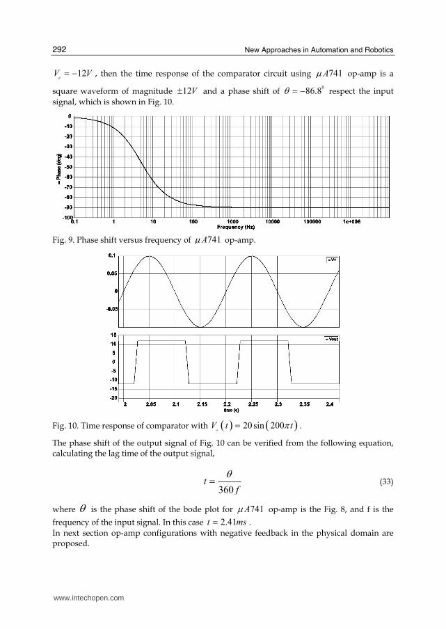
Fig. 9 for 741μA op-amp phase shift between the input and output signals.
If the noninverting input voltage is ( ) ( )0.1sin 2π+ +=v t f t V where 100+ =f Hz , the
inverting input voltage is ( ) 0− =v t V and, the supply voltages are 12=cV V and
www.intechopen.com
New Approaches in Automation and Robotics
292
12= −eV V , then the time response of the comparator circuit using 741μA op-amp is a
square waveform of magnitude 12± V and a phase shift of 0
86.8θ = − respect the input
signal, which is shown in Fig. 10.
Fig. 9. Phase shift versus frequency of 741μA op-amp.
Fig. 10. Time response of comparator with ( ) ( )20 sin 200π+ =V t t .
The phase shift of the output signal of Fig. 10 can be verified from the following equation, calculating the lag time of the output signal,
360
θ=tf
(33)
where θ is the phase shift of the bode plot for 741μA op-amp is the Fig. 8, and f is the
frequency of the input signal. In this case 2.41=t ms .
In next section op-amp configurations with negative feedback in the physical domain are proposed.
www.intechopen.com
Operational Amplifiers and Active Filters: A Bond Graph Approach
293
6. Feedback operational amplifier
An op-amp that uses feedback is called a feedback is called a feedback amplifier. A feedback amplifier is sometimes referred to as a closed loop amplifier because the feedback forms a closed loop between the input and the output. A feedback amplifier essentially consists of two parts: an op-amp and a feedback circuit. The feedback circuit can take any form whatsoever, depending on the intended application of the amplifier. This means that the feedback circuit may be made up of either passive components, active components, or combinations of both (Gayakward, 2000). A closed loop amplifier can be represented by using two blocks, one for an op-amp and another for a feedback circuit. There are four ways to connect theses two blocks. These connections are classified according to whether the voltage or current is fed back to the input in series or in parallel, as follows: 1) Voltage series feedback, 2) Voltage shunt feedback, 3) Current series feedback and 4) Current shunt feedback (Gayakward, 2000) and (Floyd & Buchla, 1999). The voltage series feedback configuration is one of the most important because this is commonly used. An in depth analysis of this configuration in the physical domain is presented in this section, computing voltage gain, input resistance, output resistance and the bandwidth.
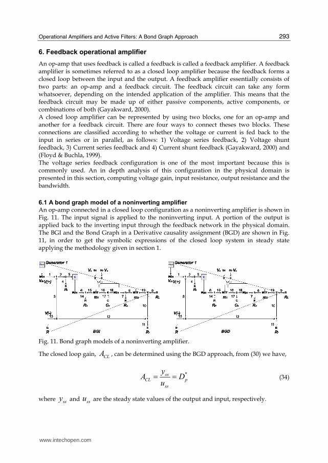
6.1 A bond graph model of a noninverting amplifier
An op-amp connected in a closed loop configuration as a noninverting amplifier is shown in Fig. 11. The input signal is applied to the noninverting input. A portion of the output is applied back to the inverting input through the feedback network in the physical domain. The BGI and the Bond Graph in a Derivative causality assignment (BGD) are shown in Fig. 11, in order to get the symbolic expressions of the closed loop system in steady state applying the methodology given in section 1.
Fig. 11. Bond graph models of a noninverting amplifier.
The closed loop gain, CLA , can be determined using the BGD approach, from (30) we have,
*ss
CL p
ss
yA D
u= = (34)
where ssy and ssu are the steady state values of the output and input, respectively.
www.intechopen.com
New Approaches in Automation and Robotics
294
We now derive the closed loop gain of the noninverting amplifier using the BGD. The key vectors of BGD are given by,
[ ][ ]
17 17 17
1 9
4 7 9 11 13 14
4 7 9 11 13 14
( ) ( ); ( ) ( ); ( ) ( )
( ) ( ); ( ) ( )
( ) ( ) ( ) ( ) ( ) ( ) ( )
( ) ( ) ( ) ( ) ( ) ( ) ( )
= = == ===
&
ind
outd
x t q t x t f t z t e t
u t e t y t e t
D t e t e t e t f t f t f t
D t f t f t f t e t e t e t
(35)
the constitutive relations are,
1=h
FC
(36)
1 1
, , , ,= ⎧ ⎫⎨ ⎬⎩ ⎭d F h
i o
L diag R R RR R
(37)
and the junction structure is,
[ ]
2 2
1 1 1
21 22 23
2
12 32
1 1
13 11 31 33
1
0 0 0 0 1 0 10
100 0 0
0
0 0 0 1 1 0 0; ;0
0 1 0 0 0 00
1 1 0 0 0 01
0 0 0 0 0 0 0
10 0 0 0 ; 0 0 0 1 1 0
;
−− −−
−= = =−
−
− −= = −
= = = =
⎡ ⎤ ⎡ ⎤⎡ ⎤ ⎢ ⎥ ⎢ ⎥⎢ ⎥ ⎢ ⎥ ⎢ ⎥⎢ ⎥ ⎢ ⎥ ⎢ ⎥⎢ ⎥ ⎢ ⎥ ⎢ ⎥⎢ ⎥ ⎢ ⎥ ⎢ ⎥⎢ ⎥ ⎢ ⎥ ⎢ ⎥⎢ ⎥ ⎢ ⎥ ⎢ ⎥⎢ ⎥ ⎢ ⎥ ⎢ ⎥⎢ ⎥ ⎢ ⎥ ⎢ ⎥⎢ ⎥⎣ ⎦ ⎣ ⎦ ⎣ ⎦⎡ ⎤⎢ ⎥⎣ ⎦
K Km m
m m m
J J J
m
m
m
KJ J
m m
KJ J J J
m0
(38)
From (21), (22), (34), (36), (37) and (38), the closed loop gain of the noninverting amplifier is,
( )
( )2 1
2
1 2 2 1
+ += Δ + + + +⎡ ⎤⎣ ⎦⎡ ⎤⎣ ⎦
L i f o
CL
o L i L f i i
R m R K R R m RRA
m R KRm R R R m m R R R RR (39)
where ( )( )Δ = + + +i L f i
R R R R RR
www.intechopen.com
Operational Amplifiers and Active Filters: A Bond Graph Approach
295
Note that the closed loop gain (39) takes account the internal parameters and the external elements connected to op-amp. A normal operation of the op-amp using the bond graph model indicates the modules of
´MTF s are1
1=m , the slew rate is sufficient of the op-amp, and2
1=m , the supply voltages
allow to obtain the output voltage depending the input voltage and the gain of the op-amp.
Considering, 1
1=m , 2
1=m and 0=oR , we obtain
( )1
1
+=+ + +⎛ ⎞⎜ ⎟⎝ ⎠
f
CL
f
f i
i
R RA
R RR R RR
K R
(40)
Applying the ( )1→∞
→∞i
CLR
K
Lim A , the ideal closed loop gain of this amplifier, ( )CL iA , is determined,
( ) 1f
CL i
RA
R= + (41)
The time response of the noninverting amplifier using 741μA op-amp, 10= ΩR K ,
190= ΩR K and the input signal is ( ) ( )0.5sin 2π=i iv t f t V where 1=
if KHz , is shown
in Fig. 12.
Fig. 12. Time response of the noninverting amplifier.
6.1.1 Input resistance of the noninverting amplifier
The input resistance of the noninverting amplifier can be determined using the BGD of Fig.
11. Considering the output ( )1f t , the submatrices
31J ,
32J and
33J from (38) are changed
by
www.intechopen.com
New Approaches in Automation and Robotics
296
[ ]23 13 331 0 0 0 0 0 ; 0= = =J J J (42)
From (21), (22), (37) and (38) the input resistance is determined by,
( )( ) ( )( )( )
+ + + + + + += + + +⎡ ⎤ ⎡ ⎤⎣ ⎦⎣ ⎦o i L f i L i L f i i
iF
f o L o L
R R R R R RR KRR R R R R R RRR
R R R R R R (43)
where ( )1 sse and ( )1 ss
f are the steady state values of the input1e and output
1f , respectively.
If 0=oR we reduce,
( )1
1= + ++ +⎛ ⎞⎜ ⎟⎝ ⎠
f
iF i
f f
RRKRR R
R R R R (44)
finally, the term + +f
i
f f
R R KRR
R R R R hence the ideal input resistance of the noninverting
amplifier ( )iF iR is defined by,
( ) 1= + +⎛ ⎞⎜ ⎟⎝ ⎠iF ii
f
KRR R
R R (45)
The result of (45) indicates that the ideal input resistance of the op-amp with feedback is ( )1+ +f
KR R R times that without feedback. In addition, the equation (43) allows to
determine the input resistance of the op-amp considering the internal parameters and
external elements for this configuration. Equation (45) can be verified in (Stanley, 1994;
Gayakward, 2000).
6.1.2 Output resistance of the noninverting amplifier
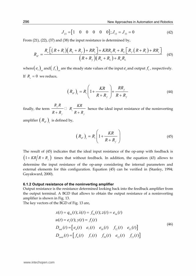
Output resistance is the resistance determined looking back into the feedback amplifier from
the output terminal. A BGD that allows to obtain the output resistance of a noninverting
amplifier is shown in Fig. 13.
The key vectors of the BGD of Fig. 13 are,
[ ][ ]
16 16 16
1 1
4 7 10 12 13
4 7 10 12 13
( ) ( ); ( ) ( ); ( ) ( )
( ) ( ); ( ) ( )
( ) ( ) ( ) ( ) ( ) ( )
( ) ( ) ( ) ( ) ( ) ( )
= = == ===
&
ind
outd
x t q t x t f t z t e t
u t e t y t f t
D t e t e t e t f t e t
D t f t f t f t e t f t
(46)
www.intechopen.com
Operational Amplifiers and Active Filters: A Bond Graph Approach
297
Fig. 13. Derivation of output resistance of a bond graph model of a noninverting amplifier.
the constitutive relations are,
1 1 1 1
, , , ,= ⎧ ⎫⎨ ⎬⎩ ⎭i o f h
L diag RR R R R
(47)
1=h
FC
(48)
and the junction structure of the BGD is,
[ ]
22 21 21 32
12 11 13 31 33
0 0 0 1 0 0 0
0 0 0 1 0 1
; ;0 0 0 1 0 0 1
1 0 1 0 0 0 0
0 0 0 0 0 1 0
0 0 0 1 ; 0
−− −
= = = = −−
= − − = = = =
⎡ ⎤ ⎡ ⎤ ⎡ ⎤⎢ ⎥ ⎢ ⎥ ⎢ ⎥⎢ ⎥ ⎢ ⎥ ⎢ ⎥⎢ ⎥ ⎢ ⎥ ⎢ ⎥⎢ ⎥ ⎢ ⎥ ⎢ ⎥⎢ ⎥ ⎢ ⎥ ⎢ ⎥⎢ ⎥ ⎢ ⎥ ⎢ ⎥⎣ ⎦ ⎣ ⎦ ⎣ ⎦
T
K
J J J J
J K J J J J
(49)
Substituting (22), (47), (49) into (21) the output resistance of a noninverting amplifier is obtained,
( )( ) ( ) ( )[ ]( ) ( )
1*1
1
− + += = = + + + + +o i f fss
oF p
i f f o iss
R R R R RReR D
f R R R KR RR R R R (50)
Calculating ( )1
lim→∞
=i
oF oFR
R R we have,
( ) ( )1
+= + + +o f
oF
f o
R R RR
R R KR R (51)
www.intechopen.com

New Approaches in Automation and Robotics
298
finally, + + + + +o f fR R R KR R R KR , the ideal output resistance ( )
oF iR of the
noninverting amplifier is given by,
( )1
=+ +
o
oF i
f
RR
KR
R R
(52)
This result shows that the ideal output resistance of the noninverting amplifier is
( )1
1+ +f
KR R R times the output resistance
oR of the op-amp. That is , the output
resistance of the op-amp with feedback is much smaller than the output resistance without feedback. In addition (52) can be verified in (Stanley, 1994; Gayakward, 2000).
6.1.3 Bandwidth of the noninverting amplifier The bandwidth of an amplifier is defined as the band (range) of frequency for which the gain remains constant. Manufacturers generally specify either the gain-bandwidth product or supply open loop gain versus frequency curve for the op-amp (Gayakward, 2000). Fig. 4 shows the open loop gain versus frequency curve of the 741μA op-amp. From this
curve for a gain of 200,000, the bandwidth is approximately 5Hz ; or the gain-bandwidth
product is 1MHz . On the other extreme, the bandwidth is approximately 1MHzwhen the gain is 1. Hence, the frequency at which the gain equals 1 is known as the unity gain bandwidth (UGB).
Since for an op-amp with a single break frequency of , the gain-bandwidth product is
constant, and equal to UGB, we can write,
( )( ) ( )( )= =o CL F
UGB K f A f (53)
where Ff bandwidth with feedback.
Therefore, the bandwidth of an feedback op-amp is,
( )( )o
F
CL
K ff
A= (54)
Fig. 14. Frequency response of the noninverting amplifier.
www.intechopen.com
Operational Amplifiers and Active Filters: A Bond Graph Approach
299
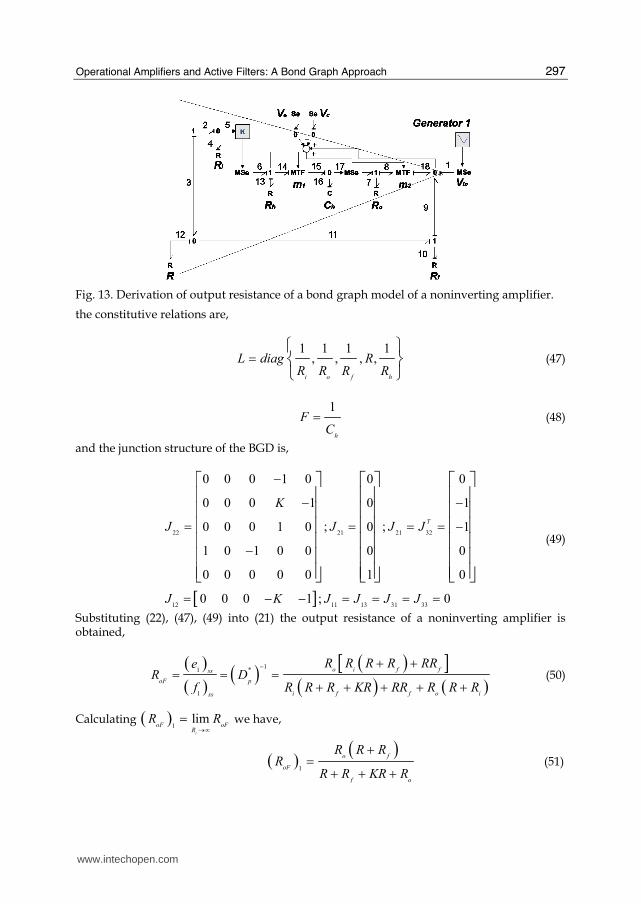
The frequency response of the noninverting amplifier based on BGI of Fig. 11, using 741μA
op-amp, 1= ΩR K , 5= ΩfR K and the input signal is ( ) ( )1.0 sin 2π=
i iv t f t V where
30=if KHz , is shown in Fig. 14.
Note that the frequency response of this amplifier indicates that the closed loop gain is
6 15.56= =CLA dB until approximately 166KHz , which is verified from (54).
6.1.4 Slew rate
Another important frequency related parameter of an op-amp is the slew rate. The slew rate is the maximum rate of change of output voltage with respect to time, usually specified in
μV s . Ideally, we would like an infinity slew rate so that the op-amp's output voltage
would change simultaneously with the input. Practical op-amps are available with slew
rates from 0.1 μV s to well above 1000 μV s . The slew rate ( )SR can be obtained by,
6
2/
10
π μ= pfV
SR V s (55)
where f is the input frequency and pV is the peak value of the output sine wave.
In order to show the effect of the slew rate of an op-amp, the time responses of the noninverting amplifier based on BGI of Fig. 11, using 741μA and 27OP op-amps,
1= ΩR K , 5= ΩfR K and the input signal is ( ) 1.0 sin(2 )π=
i iv t f t V where 30=
if KHz ,
are shown in Fig. 15. The ideal closed gain is then ( ) 6=CL iA .
Fig.15. Effect of the slew rate of the noninverting amplifier using 741μA and 27OP op-
amps.
www.intechopen.com
New Approaches in Automation and Robotics
300
From (55), the minimum slew rate of an op-amp with the previous conditions is
1.13 μ=SR V s . Therefore, the slew rate of the 27OP op-amp, which is 2.8 μV s is
enough for the input signal with the given conditions. Fig. 15, shows the output signal of the
741μA op-amp has distortion because of the slew rate is 0.5 μV s .
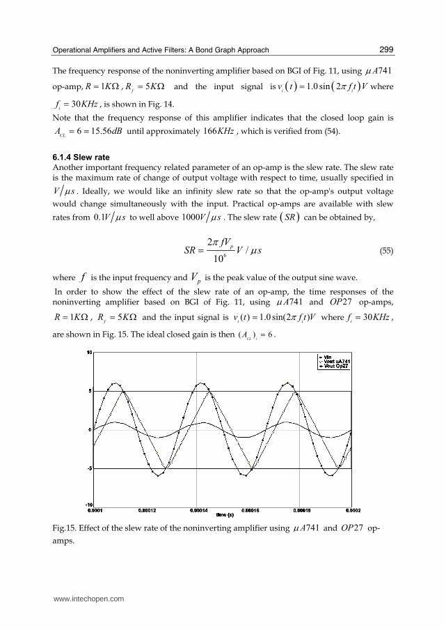
6.1.5 Supply volages
The most linear integrated circuits, particularly op-amps, use one or more differential
amplifier stages, and differential amplifiers require both a positive ( )cV and negative ( )eV
power supply for proper operation of the circuit. The supply voltages of the proposed bond graph model of an op-amp can be tested
applying an input signal ( ) 3sin(2 )π=i iv t f t , 30=
if KHz , 1= ΩR K , 5= Ω
fR K and
12=cV V and 12= −
eV V to 741μA op-amp, the time response is shown in Fig. 16.
The ideal closed loop gain is ( ) 6=CL iA , of this form the ideal output signal would be
( ) 18sin(2 )π=out iV t f t . However, the supply voltages of the op-amp are 12± V , limiting the
output signal to this rank of voltage. Next section, the op-amp integrator that is one the most interesting configurations on a bond graph model is designed.
Fig.16. Time response with slew rate and supply voltages using 741μA op-amp.
6.2 The operational amplifier integrator
An op-amp integrator simulates mathematical integration, which is basically a summing
process that determines the total area under the curve of a function (Floyd & Buchla, 1999).
A basic integrator on a BGD model is shown in Fig. 17. Notice that the feedback element is a
capacitor that forms an RC circuit with the input.
www.intechopen.com
Operational Amplifiers and Active Filters: A Bond Graph Approach
301
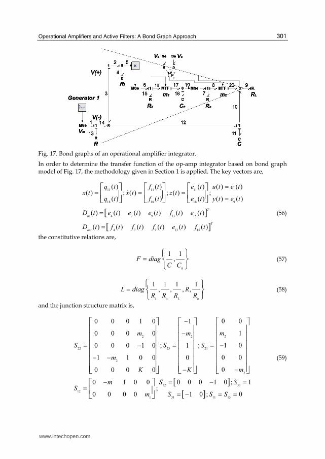
Fig. 17. Bond graphs of an operational amplifier integrator.
In order to determine the transfer function of the op-amp integrator based on bond graph model of Fig. 17, the methodology given in Section 1 is applied. The key vectors are,
[ ][ ]
11 11 11 1
18 18 18 9
4 7 9 13 15
4 7 9 13 15
( ) ( ) ( ) ( ) ( )( ) ; ( ) ; ( ) ;
( ) ( ) ( ) ( ) ( )
( ) ( ) ( ) ( ) ( ) ( )
( ) ( ) ( ) ( ) ( ) ( )
== = = ===
⎡ ⎤ ⎡ ⎤ ⎡ ⎤⎢ ⎥ ⎢ ⎥ ⎢ ⎥⎣ ⎦ ⎣ ⎦ ⎣ ⎦&
T
in
T
out
q t f t e t u t e tx t x t z t
q t f t e t y t e t
D t e t e t e t f t e t
D t f t f t f t e t f t
(56)
the constitutive relations are,
1 1
,= ⎧ ⎫⎨ ⎬⎩ ⎭hF diagC C
(57)
1 1 1 1
, , , ,= ⎧ ⎫⎨ ⎬⎩ ⎭i o L h
L diag RR R R R
(58)
and the junction structure matrix is,
[ ][ ]
22 2
22 23 21
2
2
32 33
12
31 11 131
0 00 0 0 1 0 1
10 0 0 0
; ; 1 00 0 0 1 0 1
0 01 1 0 0 0
00 0 0 0
0 0 0 1 0 ; 10 1 0 0;
1 0 ; 00 0 0 0
−−
= = = −−− −
−−= − =−= = − = =
⎡ ⎤⎡ ⎤ ⎡ ⎤ ⎢ ⎥⎢ ⎥ ⎢ ⎥ ⎢ ⎥⎢ ⎥ ⎢ ⎥ ⎢ ⎥⎢ ⎥ ⎢ ⎥ ⎢ ⎥⎢ ⎥ ⎢ ⎥ ⎢ ⎥⎢ ⎥ ⎢ ⎥ ⎢ ⎥⎢ ⎥ ⎢ ⎥⎣ ⎦ ⎣ ⎦ ⎣ ⎦⎡ ⎤⎢ ⎥⎣ ⎦
mm m
S S S
m
mK K
S SmS
S S Sm
(59)
www.intechopen.com
New Approaches in Automation and Robotics
302
From (8), (13), (57), (58) and (59) the pA matrix is,
( )( ) ( )( ) ( )
2
2 2
2 1
2 1 2
1 1
1
− −+ + += −− + Δ +
⎡ ⎤⎢ ⎥⎢ ⎥⎢ ⎥⎢ ⎥⎣ ⎦
o L i i L
h
p
o L i i L
h h
R m R R R R R m RC C
Am
R m R m KRR m KRR RC C R
(60)
where ( )[ ] 2
2Δ = + + +
o L i i L iR R R R RR m RR R
Substituting (13), (58) (59) into (9), pB is determined by,
( )( )
2
2
1
11
+= −Δ
⎡ ⎤⎢ ⎥⎢ ⎥⎢ ⎥⎣ ⎦i o L
p
o i L
h
R R m R
Bm KR R R
R
(61)
From (10), (13), (57), (58) and (59) the pC matrix is,
( )2
1 1 1−= +Δ⎡ ⎤⎢ ⎥⎣ ⎦p i o L i L
h
C R R R R m RR RC C
(62)
Finally, substituting (13), (58) and (59) into (11), pD is given by,
1= Δp o i L
D R R R (63)
The transfer function of a system represented in space state can be calculated by,
( ) 1
( )−= − +
p n p p pG s C sI A B D (64)
Substituting (60), (61), (62) and (63) into (64), the transfer function of the op-amp integrator of Fig. 17 is,
( )( )
2 2
1 1 2
2 2 2
1 2 1 1
( )+ −= Δ + Δ + + Δ + Λ
h h o o L i
h h h h L i
s CC R R sCR m Km m R RG s
s CC R s C R CRR R Km m Cm m (65)
where ( )( )2
2Λ = + +
i o LR R R m R .
Considering a normal operation of the op-amp, 1 2
1= =m m and 0=oR , we have,
1
2
1( )
11 1
−=+ + + + + +⎡ ⎛ ⎞ ⎤ ⎛ ⎞⎜ ⎟ ⎜ ⎟⎢ ⎥⎣ ⎝ ⎠ ⎦ ⎝ ⎠
h h h h
i i
G sCC R R C R R CR R
s s CRK K R K K R
(66)
www.intechopen.com
Operational Amplifiers and Active Filters: A Bond Graph Approach
303
In addition, applying 1
lim ( )→∞→∞iR
K
G s , the ideal transfer function, ( )iG s , is determined by,
1
( )iG ssRC
−= (67)
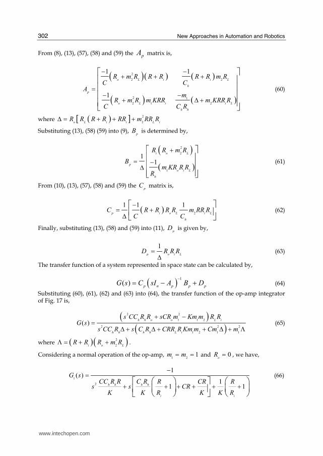
Note that, (67) is the typical transfer function of a integral controller. However, the equation (65) is the transfer function of a integral controller based on op-amp and considering their internal parameters and external elements. The time response of the integrator circuit using 741μA op-amp and 10= ΩR , 100μ=C F
and ( ) sin(2 )π=i iv t f t V where 1=
if KHz shows in Fig. 18. The output signal proves that the
bond graph model of Fig. 18, is an integrator of the input signal.
Fig. 18. Time response of the integrator.
The frequency response of the integrator circuit of Fig. 17 is shown in Fig. 19. Note that (67) is represented by Fig. 19.
Fig. 19. Frequency response of the integrator circuit.
Next section an important application of the op-amp that is an active filter in the physical domain is proposed.
www.intechopen.com
New Approaches in Automation and Robotics
304
7. Active filters using bond graph models
An electric filter is often a frequency selective circuit that passes a specified band of frequencies and blocks or attenuates signals of frequencies outside this band. Filters may be classified in a number of ways (Gayakward, 2000): 1. Analog or digital. Analog filters are designed to process analog signals, while digital
filters process analog signals using digital techniques. 2. Passive or active. Passive filters use resistors, capacitors and inductors in their
construction and the active filters employ transistor or op-amps in addition to resistors and capacitors.
An active filter offers the following advantages over a passive filter: a) Gain and frequency adjustment flexibility. b) No loading problem. c) Cost. A filter will usually conform to one of four basic response types: low-pass, high-pass, band-pass and band-reject.
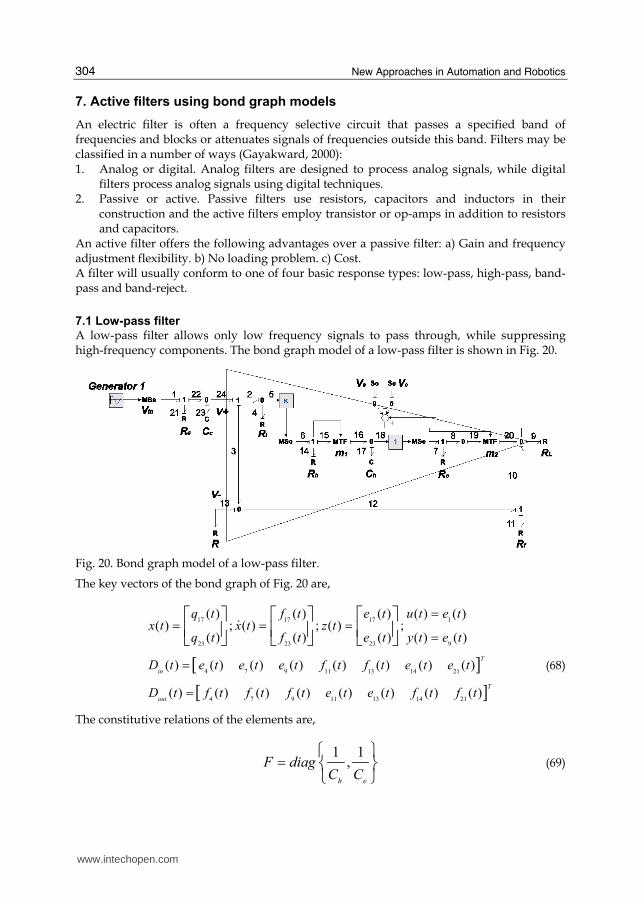
7.1 Low-pass filter
A low-pass filter allows only low frequency signals to pass through, while suppressing high-frequency components. The bond graph model of a low-pass filter is shown in Fig. 20.
Fig. 20. Bond graph model of a low-pass filter.
The key vectors of the bond graph of Fig. 20 are,
[ ][ ]
17 17 17 1
23 23 23 9
4 7 9 11 13 14 21
4 7 9 11 13 14 21
( ) ( ) ( ) ( ) ( )( ) ; ( ) ; ( ) ;
( ) ( ) ( ) ( ) ( )
( ) ( ) ( ) ( ) ( ) ( ) ( ) ( )
( ) ( ) ( ) ( ) ( ) ( ) ( ) ( )
== = = ===
⎡ ⎤ ⎡ ⎤ ⎡ ⎤⎢ ⎥ ⎢ ⎥ ⎢ ⎥⎣ ⎦ ⎣ ⎦ ⎣ ⎦&
T
in
T
out
q t f t e t u t e tx t x t z t
q t f t e t y t e t
D t e t e t e t f t f t e t e t
D t f t f t f t e t e t f t f t
(68)
The constitutive relations of the elements are,
1 1
,= ⎧ ⎫⎨ ⎬⎩ ⎭h e
F diagC C
(69)
www.intechopen.com
Operational Amplifiers and Active Filters: A Bond Graph Approach
305
1 1 1 1 1
, , , , , ,= ⎧ ⎫⎨ ⎬⎩ ⎭f
i o L h c
L diag R RR R R R R
(70)
and the junction structure is
[ ]
3 3 1
22 1 2 2 7 2 21 3 2
2 3 2 1
1 6 1
12 2 4 23
32 1 3 1 2 11 13 31 33
0 1
0 1 0
0 0 ; 0
0
0 1
0 0 00 ;
1 0 1 1
0 1 1 0 ; 0
×
× × ×
×
××
× ×
= − =−
−= =−= − = = = =
⎡ ⎤⎢ ⎥⎡ ⎤ ⎢ ⎥⎢ ⎥ ⎢ ⎥⎢ ⎥ ⎢ ⎥⎢ ⎥⎣ ⎦ ⎢ ⎥⎢ ⎥⎣ ⎦⎡ ⎤ ⎡ ⎤⎢ ⎥ ⎢ ⎥⎣ ⎦ ⎣ ⎦
T
P
S P S
P m K
mS S
S S S S S
(71)
where
1 2 2 2
0 10
;0 0
1 1
− −= − =−
⎡ ⎤ ⎡ ⎤⎢ ⎥ ⎢ ⎥⎢ ⎥ ⎣ ⎦⎢ ⎥⎣ ⎦K
P m m P (72)
From (8), (13), (69), (70) and (71), the pA matrix of the low-pass filter is,
( )( )( )
2
21 21 1 1
2
22
2
1 1
− −− − + +Δ Δ= − − + + +Δ Δ
⎡ ⎤⎡ ⎤⎣ ⎦⎢ ⎥⎢ ⎥⎢ ⎥⎡ ⎤⎢ ⎥⎣ ⎦⎣ ⎦
L i
o L f L f
h h h h h h
p
L
f o L o L
h c c h
m m KRR Rm m K m RKR R R m R R
R C C R C CA
m RRR R R m R R R
C R C C
(73)
where ( )( )[ ] ( )[ ]2
2Δ = + + + + + +
o L f i i L f i L f iR R R R R RR m RR R R R R R
Substituting (70) and (71) into (13), the pB matrix is obtained
1
0= ⎡ ⎤⎢ ⎥⎣ ⎦T
p
c
BR
(74)
Finally, from (10), (13), (69), (70) and (71), the pC matrix is
www.intechopen.com
New Approaches in Automation and Robotics
306
( )2= + +Δ Δ⎡ ⎤⎡ ⎤⎢ ⎥⎣ ⎦⎣ ⎦
L oL
p i f i f
h h
RR Rm RC R R R R R
C C (75)
and 0=pD
From (73) to (75), and (64), and considering ideal characteristics of the op-amp, 0=oR ,
= ∞iR , = ∞K and = ∞
LR , the ideal transfer function of the low-pass filter, denoted by
( )iG s is obtained ( )
1= +
CL C C
i
c C
A R CG s
s R C where 1= + f
CL
RA
R.
The ideal transfer function of the low-pass filter indicates that on the pass band the gain is
almost CLA and the pole of the system is located at the high cutoff frequency hf defined
by 1
2π=h
C C
fC R
.
The frequency response of the low-pass filter based on bond graph model using the μA741 op-amp and considering the numerical values of the Table 3 is shown in Fig 21.
R fR
LR
cR
CC
10 ΩK 10 ΩK 1 ΩK 15.9 ΩK 81 10
−× F
Table 3. Numerical values of the low-pass filter.
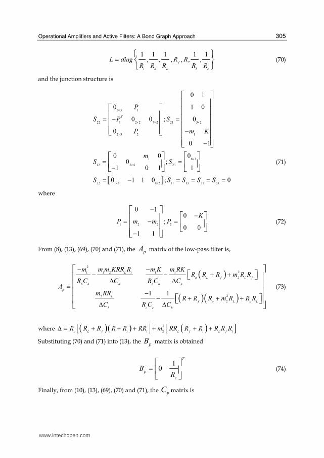
Fig. 21. Frequency response of the low-pass filter.
The Fig 21 shows that 1=hf KHz . Also, we have a first order filter, because the filter has a
pole and the rolloff rate of the filter is 20 dB per decade.
7.2 High-pass filter
A high pass filter allows only frequencies above a certain break point to pass through. In other words, it attenuates low frequency components. A first order high-pass filter on bond graph model is shown in Fig. 22.
www.intechopen.com
Operational Amplifiers and Active Filters: A Bond Graph Approach
307
Fig. 22. Bond graph model of a high-pass filter.
The mathematical model of the filter can be determined in the same manner that the low-pass filter. However, for all the remaining filters of this paper, we use the software 20-sim to know the performance of the filter on the physical domain, considering the internal characteristics of the op-amp and the external components connected to the op-amp in order to get the filter type. Using the same numerical values that the low-pass filter, the frequency response of the filter shows in Fig. 23.
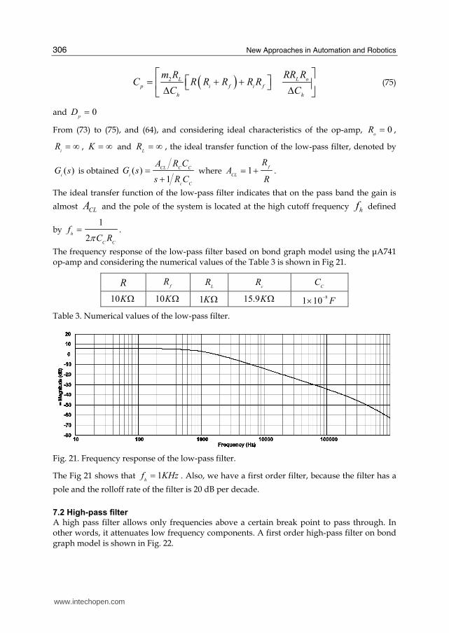
Fig. 23. Frequency response of the high-pass filter.
The Fig. 23 indicates that we have a first order filter and the low cutoff frequency Lf is
1KHz .
7.3 Band-pass filter
The band-pass filter can be thought of as a combination of high and low pass filters. It
allows only frequencies within a specified rang to pass through. In Fig. 24 a band-pass filter
on bond graph model is proposed. The characteristic of this filter is a narrow band-pass
using multiple feedback .
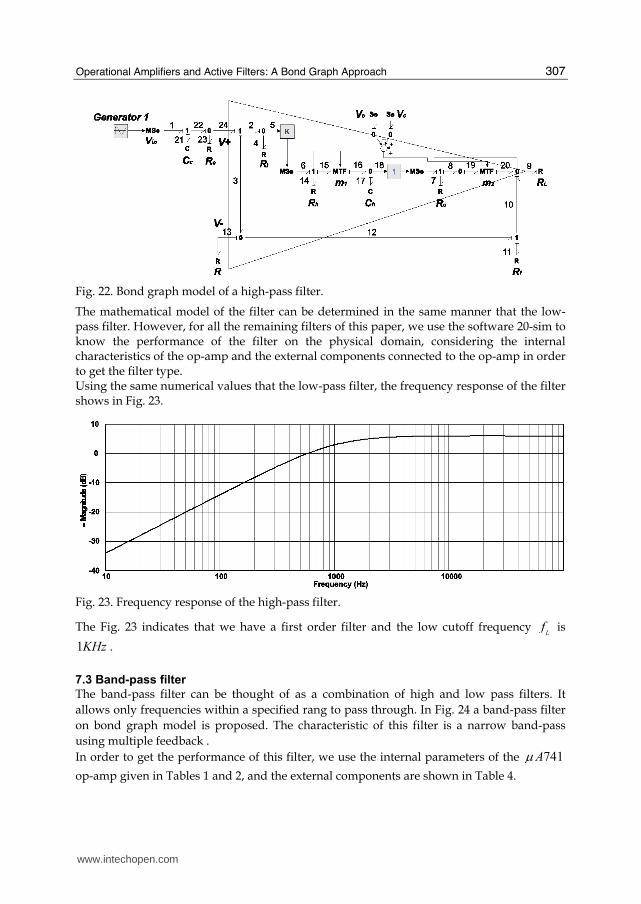
In order to get the performance of this filter, we use the internal parameters of the 741μA
op-amp given in Tables 1 and 2, and the external components are shown in Table 4.
www.intechopen.com
New Approaches in Automation and Robotics
308
Fig. 24. Bond graph model of a band-pass filter.
cR f
R LR
2cR
cC
2cC
4.77 ΩK 100 ΩK 10 ΩK 0.2 ΩK 0.01μF 0.01μF
Table 4. Numerical values of the external components
The frequency response of the band-pass filter is shown in Fig. 25.
Fig. 25. Frequency response of the band-pass filter.
Note that, the response of the filter allows to pass the frequency component of 1KHz with
a closed loop gain of 10 and the low and high frequencies respect to 1KHz have a small magnitude.
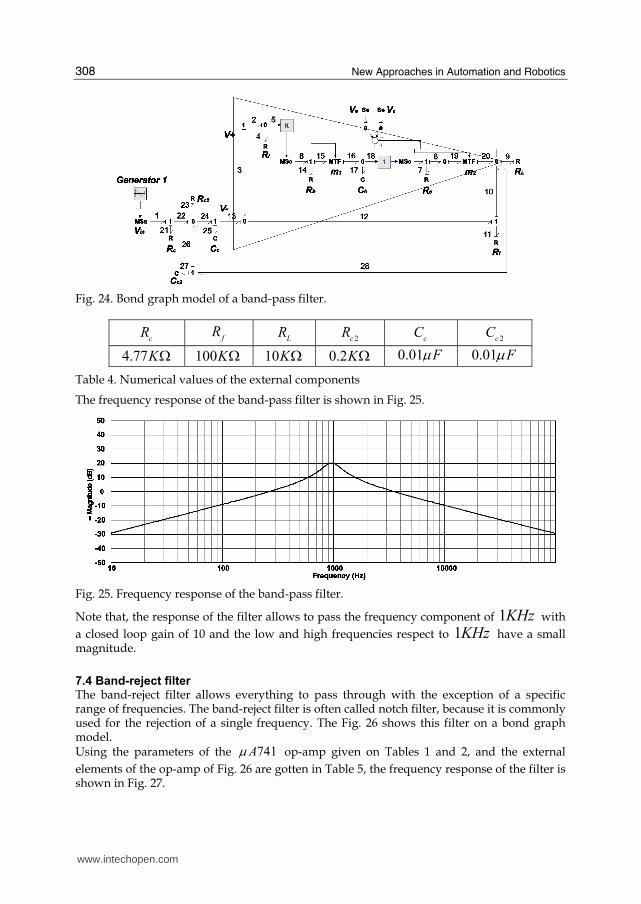
7.4 Band-reject filter The band-reject filter allows everything to pass through with the exception of a specific range of frequencies. The band-reject filter is often called notch filter, because it is commonly used for the rejection of a single frequency. The Fig. 26 shows this filter on a bond graph model. Using the parameters of the 741μA op-amp given on Tables 1 and 2, and the external
elements of the op-amp of Fig. 26 are gotten in Table 5, the frequency response of the filter is shown in Fig. 27.
www.intechopen.com
Operational Amplifiers and Active Filters: A Bond Graph Approach
309
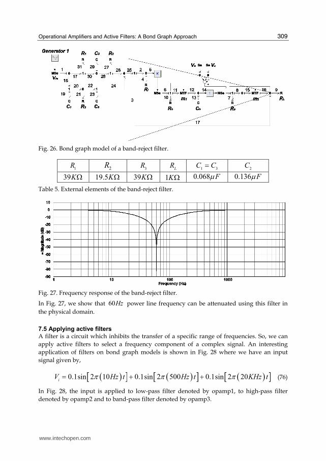
Fig. 26. Bond graph model of a band-reject filter.
1R 2R
3R
LR
1 3=C C
2C
39 ΩK 19.5 ΩK 39 ΩK 1 ΩK 0.068μF 0.136μF
Table 5. External elements of the band-reject filter.
Fig. 27. Frequency response of the band-reject filter.
In Fig. 27, we show that 60Hz power line frequency can be attenuated using this filter in
the physical domain.
7.5 Applying active filters
A filter is a circuit which inhibits the transfer of a specific range of frequencies. So, we can
apply active filters to select a frequency component of a complex signal. An interesting
application of filters on bond graph models is shown in Fig. 28 where we have an input
signal given by,
( )[ ] ( )[ ] ( )[ ]0.1sin 2 10 0.1sin 2 500 0.1sin 2 20π π π= + +iV Hz t Hz t KHz t (76)
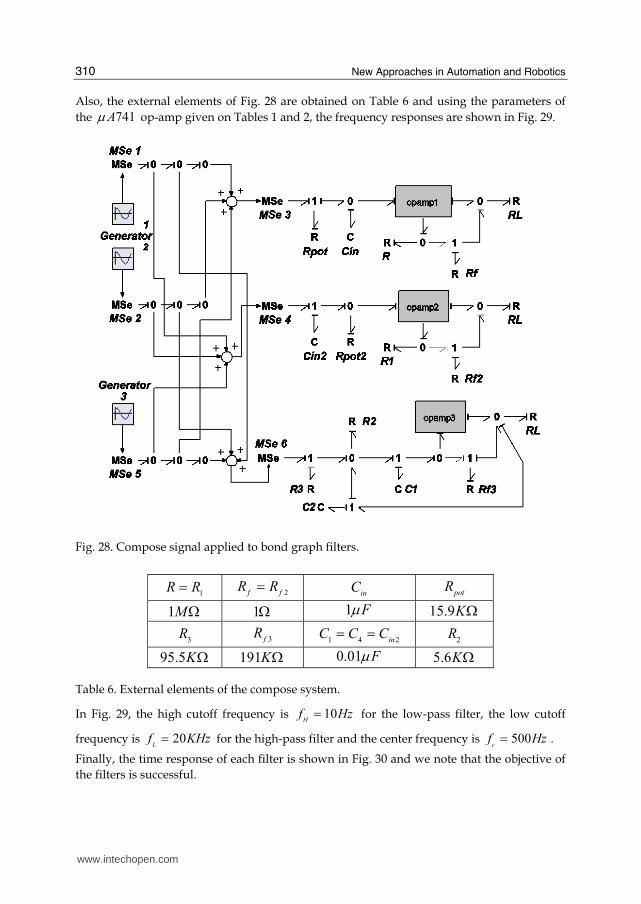
In Fig. 28, the input is applied to low-pass filter denoted by opamp1, to high-pass filter
denoted by opamp2 and to band-pass filter denoted by opamp3.
www.intechopen.com
New Approaches in Automation and Robotics
310
Also, the external elements of Fig. 28 are obtained on Table 6 and using the parameters of
the 741μA op-amp given on Tables 1 and 2, the frequency responses are shown in Fig. 29.
Fig. 28. Compose signal applied to bond graph filters.
1=R R 2
=f fR R
inC pot
R
1 ΩM 1Ω 1μF 15.9 ΩK
3R 3f
R 1 4 2= =
inC C C
2R
95.5 ΩK 191 ΩK 0.01μF 5.6 ΩK
Table 6. External elements of the compose system.
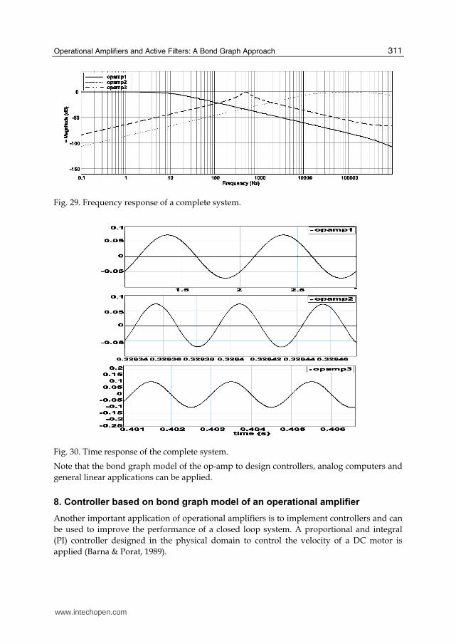
In Fig. 29, the high cutoff frequency is 10=Hf Hz for the low-pass filter, the low cutoff
frequency is 20=Lf KHz for the high-pass filter and the center frequency is 500=
cf Hz .
Finally, the time response of each filter is shown in Fig. 30 and we note that the objective of
the filters is successful.
www.intechopen.com
Operational Amplifiers and Active Filters: A Bond Graph Approach
311
Fig. 29. Frequency response of a complete system.
Fig. 30. Time response of the complete system.
Note that the bond graph model of the op-amp to design controllers, analog computers and
general linear applications can be applied.
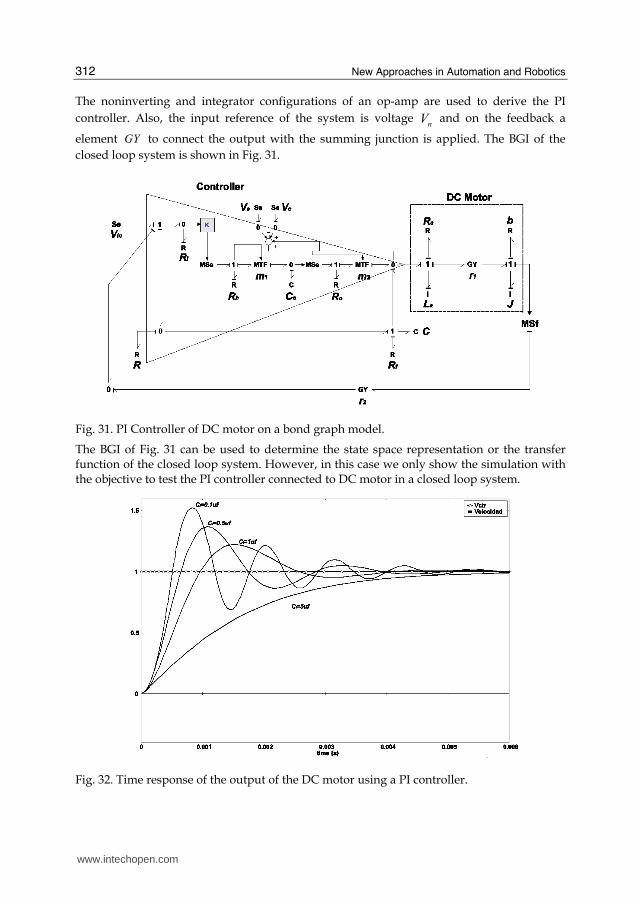
8. Controller based on bond graph model of an operational amplifier
Another important application of operational amplifiers is to implement controllers and can
be used to improve the performance of a closed loop system. A proportional and integral
(PI) controller designed in the physical domain to control the velocity of a DC motor is
applied (Barna & Porat, 1989).
www.intechopen.com
New Approaches in Automation and Robotics
312
The noninverting and integrator configurations of an op-amp are used to derive the PI
controller. Also, the input reference of the system is voltage nV and on the feedback a
element GY to connect the output with the summing junction is applied. The BGI of the
closed loop system is shown in Fig. 31.
Fig. 31. PI Controller of DC motor on a bond graph model.
The BGI of Fig. 31 can be used to determine the state space representation or the transfer function of the closed loop system. However, in this case we only show the simulation with the objective to test the PI controller connected to DC motor in a closed loop system.
Fig. 32. Time response of the output of the DC motor using a PI controller.
www.intechopen.com

Operational Amplifiers and Active Filters: A Bond Graph Approach
313
The time response of the output using a 741μA op-amp, 10= ΩR K , 90= ΩfR K ,
2= ΩaR , 0.01=
aL mH ,
20.001=J Kgm and 1 / /=b Nm rad s , is shown in Fig. 32.
Note that the PI Controller yields a steady state output equal to input reference of the
system and the transient response depends of the parameters of the system and controller.
9. Conclusions
In this work an operational amplifier is shown in a bond graph model. The proposed bond
graph takes account the input and output resistances, open loop gain, supply voltages, slew
rate and frequency compensation of an operational amplifier. Therefore, an advantage of
this model is to determine the performance of applications based on operational amplifiers
considering the type of linear integrated circuit to obtain the internal parameters from the
data sheets. Finally, open loop and closed loop configurations of the operational amplifier in
the physical domain have been shown.
10. References
Arpad Barna and Dan I. Porat, (1989). Operational Amplifiers, John Wiley & Sons,ISBN:0-471-
63764-5, Canada
C. Sueur, G. Dauphin-Tanguy, (1991), Bond graph approach for structural analysis of MIMO
linear systems, Journal of the Franklin Institute, vol. 328, no.1 , (55-70).
Dean C. Karnopp, Ronald C. Rosenberg, (1975). System Dynamics: A Unified Approach, Wiley,
John & Sons,
Forbes T. Brown (2001)., Engineering System Dynamics, Marcel Dekker Inc, ISBN:0-8247-0616-
1, United States of America.
Gilberto Gonzalez, Dauphin- Tanguy G. Galindo R and De Leon J. (2005), Steady State Error
for a Closed Loop Physical System with a Bond Graph Approach, Proceedings of
International Conference on Bond Graph Modeling and Simulation, pp. 107-112, ISBN:1-
56555-287-3, New Orleans, January 2005, SCS.
Norman S. Nise, (2000). Control Systems Engineering, John Wiley & Sons, ISBN:970-24-0254-9,
United States of America.
Peter Gawthrop, Lorcan Smith (1996)., Metamodelling, Prentice-Hall,ISBN:0-13-489824-9,
Great Britain.
P.E. Wellstead, (1979). Physical System Modelling, Academic Press, ISBN:0-12-744380-0
London.
P. J. Gawthrop and D. Palmer, (2003). A bicausal bond graph representation of operational
amplifiers", Proceedings of the Institution of Mechanical Engineers Part I: Journal
Systems and Control Engineering, Vol. 217
Ramakant A. Gayakward, (2000), Op-amps and Linear Integrated Circuit, Prentice Hall,
ISBN:0-13-280868-4, United States of America.
www.intechopen.com

New Approaches in Automation and Robotics
314
Thomas L. Floyd and David Buchla, (1999), Basic Operational Amplifiers and Linear Integrated
Circuits, Prentice-Hall, ISBN:0-13-082987-0, United States of America.
William D. Stanley, (1994). Operational Amplifiers with Linear Integrated Circuits, Maxwell
Macmillan International
20-Sim, Controllab Products (2007) B. V., 20-Sim, http://www.20sim.com/ product/20sim.html
www.intechopen.com

New Approaches in Automation and RoboticsEdited by Harald Aschemann
ISBN 978-3-902613-26-4Hard cover, 392 pagesPublisher I-Tech Education and PublishingPublished online 01, May, 2008Published in print edition May, 2008
InTech EuropeUniversity Campus STeP Ri Slavka Krautzeka 83/A 51000 Rijeka, Croatia Phone: +385 (51) 770 447 Fax: +385 (51) 686 166www.intechopen.com
InTech ChinaUnit 405, Office Block, Hotel Equatorial Shanghai No.65, Yan An Road (West), Shanghai, 200040, China
Phone: +86-21-62489820 Fax: +86-21-62489821
The book New Approaches in Automation and Robotics offers in 22 chapters a collection of recentdevelopments in automation, robotics as well as control theory. It is dedicated to researchers in science andindustry, students, and practicing engineers, who wish to update and enhance their knowledge on modernmethods and innovative applications. The authors and editor of this book wish to motivate people, especiallyunder-graduate students, to get involved with the interesting field of robotics and mechatronics. We hope thatthe ideas and concepts presented in this book are useful for your own work and could contribute to problemsolving in similar applications as well. It is clear, however, that the wide area of automation and robotics canonly be highlighted at several spots but not completely covered by a single book.
How to referenceIn order to correctly reference this scholarly work, feel free to copy and paste the following:
Gilberto Gonzalez and Roberto Tapia (2008). Operational Amplifiers and Active Filters: A Bond GraphApproach, New Approaches in Automation and Robotics, Harald Aschemann (Ed.), ISBN: 978-3-902613-26-4,InTech, Available from:http://www.intechopen.com/books/new_approaches_in_automation_and_robotics/operational_amplifiers_and_active_filters__a_bond_graph_approach
Related Documents


