LM101AQML www.ti.com SNOSAI0A – JANUARY 2006 – REVISED MARCH 2013 LM101AQML Operational Amplifiers Check for Samples: LM101AQML 1FEATURES • Offset Current 20 nA Maximum Over Temperature 2• Available with Radiation Guarantee • Ensured Drift Characteristics • Offset Voltage 3 mV Maximum Over • Offsets Specified Over Entire Common Mode Temperature and Supply Voltage Ranges • Input Current 100 nA Maximum Over • Slew Rate of 10 V/μS as a Summing Amplifier Temperature DESCRIPTION The LM101A is a general purpose operational amplifier which features improved performance over industry standards such as the LM709. Advanced processing techniques make possible an order of magnitude reduction in input currents, and a redesign of the biasing circuitry reduces the temperature drift of input current. Improved specifications include: • Offset voltage 3 mV maximum over temperature • Input current 100 nA maximum over temperature • Offset current 20 nA maximum over temperature • Specified drift characteristics • Offsets ensured over entire common mode and supply voltage ranges • Slew rate of 10V/μs as a summing amplifier – This amplifier offers many features which make its application nearly foolproof: overload protection on the input and output, no latch-up when the common mode range is exceeded, and freedom from oscillations and compensation with a single 30 pF capacitor. It has advantages over internally compensated amplifiers in that the frequency compensation can be tailored to the particular application. For example, in low frequency circuits it can be overcompensated for increased stability margin. Or the compensation can be optimized to give more than a factor of ten improvement in high frequency performance for most applications. – In addition, the device provides better accuracy and lower noise in high impedance circuitry. The low input currents also make it particularly well suited for long interval integrators or timers, sample and hold circuits and low frequency waveform generators. Further, replacing circuits where matched transistor pairs buffer the inputs of conventional IC op amps, it can give lower offset voltage and a drift at a lower cost. 1 Please be aware that an important notice concerning availability, standard warranty, and use in critical applications of Texas Instruments semiconductor products and disclaimers thereto appears at the end of this data sheet. 2All trademarks are the property of their respective owners. PRODUCTION DATA information is current as of publication date. Copyright © 2006–2013, Texas Instruments Incorporated Products conform to specifications per the terms of the Texas Instruments standard warranty. Production processing does not necessarily include testing of all parameters.

Welcome message from author
This document is posted to help you gain knowledge. Please leave a comment to let me know what you think about it! Share it to your friends and learn new things together.
Transcript

LM101AQML
www.ti.com SNOSAI0A –JANUARY 2006–REVISED MARCH 2013
LM101AQML Operational AmplifiersCheck for Samples: LM101AQML
1FEATURES • Offset Current 20 nA Maximum OverTemperature
2• Available with Radiation Guarantee• Ensured Drift Characteristics• Offset Voltage 3 mV Maximum Over• Offsets Specified Over Entire Common ModeTemperature
and Supply Voltage Ranges• Input Current 100 nA Maximum Over• Slew Rate of 10 V/µS as a Summing AmplifierTemperature
DESCRIPTIONThe LM101A is a general purpose operational amplifier which features improved performance over industrystandards such as the LM709. Advanced processing techniques make possible an order of magnitude reductionin input currents, and a redesign of the biasing circuitry reduces the temperature drift of input current. Improvedspecifications include:• Offset voltage 3 mV maximum over temperature• Input current 100 nA maximum over temperature• Offset current 20 nA maximum over temperature• Specified drift characteristics• Offsets ensured over entire common mode and supply voltage ranges• Slew rate of 10V/μs as a summing amplifier
– This amplifier offers many features which make its application nearly foolproof: overload protection on theinput and output, no latch-up when the common mode range is exceeded, and freedom from oscillationsand compensation with a single 30 pF capacitor. It has advantages over internally compensated amplifiersin that the frequency compensation can be tailored to the particular application. For example, in lowfrequency circuits it can be overcompensated for increased stability margin. Or the compensation can beoptimized to give more than a factor of ten improvement in high frequency performance for mostapplications.
– In addition, the device provides better accuracy and lower noise in high impedance circuitry. The low inputcurrents also make it particularly well suited for long interval integrators or timers, sample and hold circuitsand low frequency waveform generators. Further, replacing circuits where matched transistor pairs bufferthe inputs of conventional IC op amps, it can give lower offset voltage and a drift at a lower cost.
1
Please be aware that an important notice concerning availability, standard warranty, and use in critical applications ofTexas Instruments semiconductor products and disclaimers thereto appears at the end of this data sheet.
2All trademarks are the property of their respective owners.
PRODUCTION DATA information is current as of publication date. Copyright © 2006–2013, Texas Instruments IncorporatedProducts conform to specifications per the terms of the TexasInstruments standard warranty. Production processing does notnecessarily include testing of all parameters.
LM101AQML
SNOSAI0A –JANUARY 2006–REVISED MARCH 2013 www.ti.com
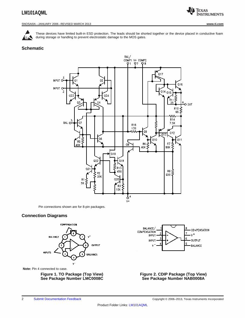
These devices have limited built-in ESD protection. The leads should be shorted together or the device placed in conductive foamduring storage or handling to prevent electrostatic damage to the MOS gates.
Schematic
Pin connections shown are for 8-pin packages.
Connection Diagrams
Note: Pin 4 connected to case.
Figure 1. TO Package (Top View) Figure 2. CDIP Package (Top View)See Package Number LMC0008C See Package Number NAB0008A
2 Submit Documentation Feedback Copyright © 2006–2013, Texas Instruments Incorporated
Product Folder Links: LM101AQML
LM101AQML
www.ti.com SNOSAI0A –JANUARY 2006–REVISED MARCH 2013
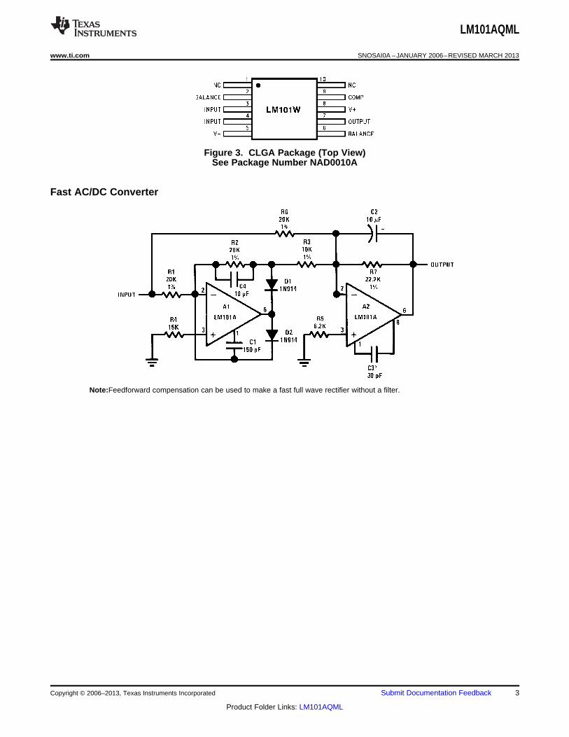
Figure 3. CLGA Package (Top View)See Package Number NAD0010A
Fast AC/DC Converter
Note:Feedforward compensation can be used to make a fast full wave rectifier without a filter.
Copyright © 2006–2013, Texas Instruments Incorporated Submit Documentation Feedback 3
Product Folder Links: LM101AQML
LM101AQML
SNOSAI0A –JANUARY 2006–REVISED MARCH 2013 www.ti.com
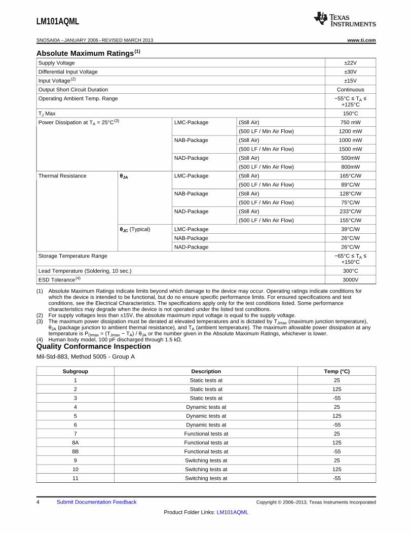
Absolute Maximum Ratings (1)
Supply Voltage ±22V
Differential Input Voltage ±30V
Input Voltage (2) ±15V
Output Short Circuit Duration Continuous
Operating Ambient Temp. Range −55°C ≤ TA ≤+125°C
TJ Max 150°C
Power Dissipation at TA = 25°C (3) LMC-Package (Still Air) 750 mW
(500 LF / Min Air Flow) 1200 mW
NAB-Package (Still Air) 1000 mW
(500 LF / Min Air Flow) 1500 mW
NAD-Package (Still Air) 500mW
(500 LF / Min Air Flow) 800mW
Thermal Resistance θJA LMC-Package (Still Air) 165°C/W
(500 LF / Min Air Flow) 89°C/W
NAB-Package (Still Air) 128°C/W
(500 LF / Min Air Flow) 75°C/W
NAD-Package (Still Air) 233°C/W
(500 LF / Min Air Flow) 155°C/W
θJC (Typical) LMC-Package 39°C/W
NAB-Package 26°C/W
NAD-Package 26°C/W
Storage Temperature Range −65°C ≤ TA ≤+150°C
Lead Temperature (Soldering, 10 sec.) 300°C
ESD Tolerance (4) 3000V
(1) Absolute Maximum Ratings indicate limits beyond which damage to the device may occur. Operating ratings indicate conditions forwhich the device is intended to be functional, but do no ensure specific performance limits. For ensured specifications and testconditions, see the Electrical Characteristics. The specifications apply only for the test conditions listed. Some performancecharacteristics may degrade when the device is not operated under the listed test conditions.
(2) For supply voltages less than ±15V, the absolute maximum input voltage is equal to the supply voltage.(3) The maximum power dissipation must be derated at elevated temperatures and is dictated by TJmax (maximum junction temperature),
θJA (package junction to ambient thermal resistance), and TA (ambient temperature). The maximum allowable power dissipation at anytemperature is PDmax = (TJmax − TA) / θJA or the number given in the Absolute Maximum Ratings, whichever is lower.
(4) Human body model, 100 pF discharged through 1.5 kΩ.Quality Conformance InspectionMil-Std-883, Method 5005 - Group A
Subgroup Description Temp (°C)
1 Static tests at 25
2 Static tests at 125
3 Static tests at -55
4 Dynamic tests at 25
5 Dynamic tests at 125
6 Dynamic tests at -55
7 Functional tests at 25
8A Functional tests at 125
8B Functional tests at -55
9 Switching tests at 25
10 Switching tests at 125
11 Switching tests at -55
4 Submit Documentation Feedback Copyright © 2006–2013, Texas Instruments Incorporated
Product Folder Links: LM101AQML
LM101AQML
www.ti.com SNOSAI0A –JANUARY 2006–REVISED MARCH 2013
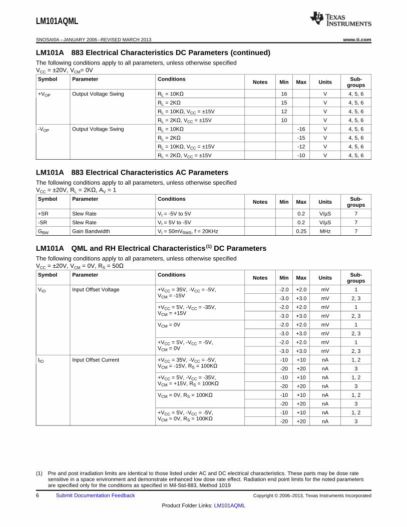
LM101A 883 Electrical Characteristics DC ParametersThe following conditions apply to all parameters, unless otherwise specifiedVCC = ±20V, VCM= 0V
Symbol Parameter Conditions Sub-Notes Min Max Units groups
VIO Input Offset Voltage VCM = -15V, RS = 50Ω -2.0 2.0 mV 1
-3.0 3.0 mV 2, 3
VCM = 15V, RS = 50Ω -2.0 2.0 mV 1
-3.0 3.0 mV 2, 3
RS = 50Ω -2.0 2.0 mV 1
-3.0 3.0 mV 2, 3
VCC = ±5V, RS = 50Ω -2.0 2.0 mV 1
-3.0 3.0 mV 2, 3
IIO Input Offset Current VCM = -15V -10 10 nA 1
-20 20 nA 2, 3
VCM = 15V -10 10 nA 1
-20 20 nA 2, 3
-10 10 nA 1
-20 20 nA 2, 3
VCC = ±5V -10 10 nA 1
-20 20 nA 2, 3
±IIB Input Bias Current VCM = -15V 1.0 75 nA 1
1.0 100 nA 2, 3
VCM = 15V 1.0 75 nA 1
1.0 100 nA 2, 3
1.0 75 nA 1
1.0 100 nA 2, 3
VCC = ±5V 1.0 75 nA 1
1.0 100 nA 2, 3
PSRR+ Power Supply Rejection Ratio +VCC = +20V and +5V, -VCC=-20V, 80 dB 1, 2, 3RS=50ΩPSRR- Power Supply Rejection Ratio +VCC = +20V, 80 dB 1, 2, 3-VCC= -20V and -5V, RS=50ΩCMRR Common Mode Rejection Ratio -15V ≤ VCM ≤ 15V, RS = 50Ω 80 dB 1, 2, 3
ICC Supply Current 3.0 mA 1
2.5 mA 2
3.5 mA 3
+VIO Adj Input Offset Voltage Adjust 4.0 mV 1, 2, 3
−VIO Adj Input Offset Voltage Adjust -4.0 mV 1, 2, 3
+IOS Short Circuit Current -45 -7.0 mA 1, 2, 3
-IOS Short Circuit Current 7.0 45 mA 1, 2, 3
VI Input Voltage Range VCC = ±20V See (1) -15 15 V 1, 2, 3
+AVS Large Signal Gain VCC = ±15V, RS = 0, RL=2KΩ, VO 50 V/mV 4=10V 25 V/mV 5, 6
-AVS Large Signal Gain VCC = ±15V, RS = 0, RL=2KΩ, VO 50 V/mV 4=-10V 25 V/mV 5, 6
RI Input Resistance See (2) 1.5 MΩ 4
see (2) 0.5 MΩ 5, 6
(1) Parameter specified by the input conditions of several DC parameters(2) Parameter specified by design, not tested.
Copyright © 2006–2013, Texas Instruments Incorporated Submit Documentation Feedback 5
Product Folder Links: LM101AQML
LM101AQML
SNOSAI0A –JANUARY 2006–REVISED MARCH 2013 www.ti.com
LM101A 883 Electrical Characteristics DC Parameters (continued)The following conditions apply to all parameters, unless otherwise specifiedVCC = ±20V, VCM= 0V
Symbol Parameter Conditions Sub-Notes Min Max Units groups
+VOP Output Voltage Swing RL = 10KΩ 16 V 4, 5, 6
RL = 2KΩ 15 V 4, 5, 6
RL = 10KΩ, VCC = ±15V 12 V 4, 5, 6
RL = 2KΩ, VCC = ±15V 10 V 4, 5, 6
-VOP Output Voltage Swing RL = 10KΩ -16 V 4, 5, 6
RL = 2KΩ -15 V 4, 5, 6
RL = 10KΩ, VCC = ±15V -12 V 4, 5, 6
RL = 2KΩ, VCC = ±15V -10 V 4, 5, 6
LM101A 883 Electrical Characteristics AC ParametersThe following conditions apply to all parameters, unless otherwise specifiedVCC = ±20V, RL = 2KΩ, AV = 1
Symbol Parameter Conditions Sub-Notes Min Max Units groups
+SR Slew Rate VI = -5V to 5V 0.2 V/µS 7
-SR Slew Rate VI = 5V to -5V 0.2 V/µS 7
GBW Gain Bandwidth VI = 50mVRMS, f = 20KHz 0.25 MHz 7
LM101A QML and RH Electrical Characteristics (1) DC ParametersThe following conditions apply to all parameters, unless otherwise specifiedVCC = ±20V, VCM = 0V, RS = 50ΩSymbol Parameter Conditions Sub-Notes Min Max Units groups
VIO Input Offset Voltage +VCC = 35V, -VCC = -5V, -2.0 +2.0 mV 1VCM = -15V -3.0 +3.0 mV 2, 3
+VCC = 5V, -VCC = -35V, -2.0 +2.0 mV 1VCM = +15V -3.0 +3.0 mV 2, 3
VCM = 0V -2.0 +2.0 mV 1
-3.0 +3.0 mV 2, 3
+VCC = 5V, -VCC = -5V, -2.0 +2.0 mV 1VCM = 0V -3.0 +3.0 mV 2, 3
IIO Input Offset Current +VCC = 35V, -VCC = -5V, -10 +10 nA 1, 2VCM = -15V, RS = 100KΩ -20 +20 nA 3
+VCC = 5V, -VCC = -35V, -10 +10 nA 1, 2VCM = +15V, RS = 100KΩ -20 +20 nA 3
VCM = 0V, RS = 100KΩ -10 +10 nA 1, 2
-20 +20 nA 3
+VCC = 5V, -VCC = -5V, -10 +10 nA 1, 2VCM = 0V, RS = 100KΩ -20 +20 nA 3
(1) Pre and post irradiation limits are identical to those listed under AC and DC electrical characteristics. These parts may be dose ratesensitive in a space environment and demonstrate enhanced low dose rate effect. Radiation end point limits for the noted parametersare specified only for the conditions as specified in Mil-Std-883, Method 1019
6 Submit Documentation Feedback Copyright © 2006–2013, Texas Instruments Incorporated
Product Folder Links: LM101AQML
LM101AQML
www.ti.com SNOSAI0A –JANUARY 2006–REVISED MARCH 2013
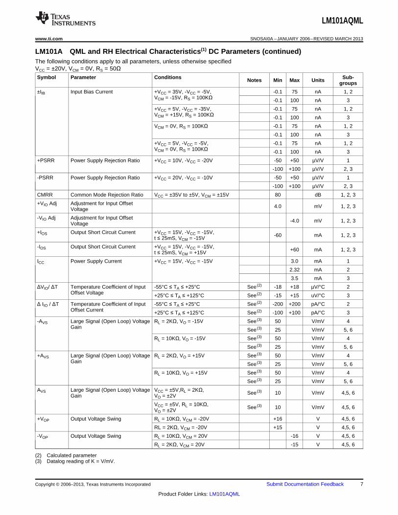
LM101A QML and RH Electrical Characteristics(1) DC Parameters (continued)The following conditions apply to all parameters, unless otherwise specifiedVCC = ±20V, VCM = 0V, RS = 50ΩSymbol Parameter Conditions Sub-Notes Min Max Units groups
±IIB Input Bias Current +VCC = 35V, -VCC = -5V, -0.1 75 nA 1, 2VCM = -15V, RS = 100KΩ -0.1 100 nA 3
+VCC = 5V, -VCC = -35V, -0.1 75 nA 1, 2VCM = +15V, RS = 100KΩ -0.1 100 nA 3
VCM = 0V, RS = 100KΩ -0.1 75 nA 1, 2
-0.1 100 nA 3
+VCC = 5V, -VCC = -5V, -0.1 75 nA 1, 2VCM = 0V, RS = 100KΩ -0.1 100 nA 3
+PSRR Power Supply Rejection Ratio +VCC = 10V, -VCC = -20V -50 +50 µV/V 1
-100 +100 µV/V 2, 3
-PSRR Power Supply Rejection Ratio +VCC = 20V, -VCC = -10V -50 +50 µV/V 1
-100 +100 µV/V 2, 3
CMRR Common Mode Rejection Ratio VCC = ±35V to ±5V, VCM = ±15V 80 dB 1, 2, 3
+VIO Adj Adjustment for Input Offset 4.0 mV 1, 2, 3Voltage
-VIO Adj Adjustment for Input Offset -4.0 mV 1, 2, 3Voltage
+IOS Output Short Circuit Current +VCC = 15V, -VCC = -15V, -60 mA 1, 2, 3t ≤ 25mS, VCM = -15V
-IOS Output Short Circuit Current +VCC = 15V, -VCC = -15V, +60 mA 1, 2, 3t ≤ 25mS, VCM = +15V
ICC Power Supply Current +VCC = 15V, -VCC = -15V 3.0 mA 1
2.32 mA 2
3.5 mA 3
ΔVIO/ ΔT Temperature Coefficient of Input -55°C ≤ TA ≤ +25°C See (2) -18 +18 µV/°C 2Offset Voltage +25°C ≤ TA ≤ +125°C See (2) -15 +15 uV/°C 3
Δ IIO / ΔT Temperature Coefficient of Input -55°C ≤ TA ≤ +25°C See (2) -200 +200 pA/°C 2Offset Current +25°C ≤ TA ≤ +125°C See (2) -100 +100 pA/°C 3
-AVS Large Signal (Open Loop) Voltage RL = 2KΩ, VO = -15V See (3) 50 V/mV 4Gain See (3) 25 V/mV 5, 6
RL = 10KΩ, VO = -15V See (3) 50 V/mV 4
See (3) 25 V/mV 5, 6
+AVS Large Signal (Open Loop) Voltage RL = 2KΩ, VO = +15V See (3) 50 V/mV 4Gain See (3) 25 V/mV 5, 6
RL = 10KΩ, VO = +15V See (3) 50 V/mV 4
See (3) 25 V/mV 5, 6
AVS Large Signal (Open Loop) Voltage VCC = ±5V,RL = 2KΩ, See (3) 10 V/mV 4,5, 6Gain VO = ±2V
VCC = ±5V, RL = 10KΩ, See (3) 10 V/mV 4,5, 6VO = ±2V
+VOP Output Voltage Swing RL = 10KΩ, VCM = -20V +16 V 4,5, 6
RL = 2KΩ, VCM = -20V +15 V 4,5, 6
-VOP Output Voltage Swing RL = 10KΩ, VCM = 20V -16 V 4,5, 6
RL = 2KΩ, VCM = 20V -15 V 4,5, 6
(2) Calculated parameter(3) Datalog reading of K = V/mV.
Copyright © 2006–2013, Texas Instruments Incorporated Submit Documentation Feedback 7
Product Folder Links: LM101AQML
LM101AQML
SNOSAI0A –JANUARY 2006–REVISED MARCH 2013 www.ti.com
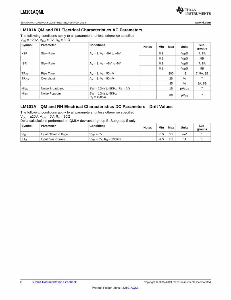
LM101A QM and RH Electrical Characteristics AC ParametersThe following conditions apply to all parameters, unless otherwise specifiedVCC = ±20V, VCM = 0V, RS = 50ΩSymbol Parameter Conditions Sub-Notes Min Max Units groups
+SR Slew Rate AV = 1, VI = -5V to +5V 0.3 V/µS 7, 8A
0.2 V/µS 8B
-SR Slew Rate AV = 1, VI = +5V to -5V 0.3 V/µS 7, 8A
0.2 V/µS 8B
TRTR Rise Time AV = 1, VI = 50mV 800 nS 7, 8A, 8B
TROS Overshoot AV = 1, VI = 50mV 25 % 7
35 % 8A, 8B
NIBB Noise Broadband BW = 10Hz to 5KHz, RS = 0Ω 15 µVRMS 7
NIPC Noise Popcorn BW = 10Hz to 5KHz, 80 µVPK 7RS = 100KΩ
LM101A QM and RH Electrical Characteristics DC Parameters Drift ValuesThe following conditions apply to all parameters, unless otherwise specifiedVCC = ±20V, VCM = 0V, RS = 50ΩDelta calculations performed on QMLV devices at group B, Subgroup 5 only.
Symbol Parameter Conditions Sub-Notes Min Max Units groups
VIO Input Offset Voltage VCM = 0V -0.5 0.5 mV 1
± IIB Input Bias Current VCM = 0V, RS = 100KΩ -7.5 7.5 nA 1
8 Submit Documentation Feedback Copyright © 2006–2013, Texas Instruments Incorporated
Product Folder Links: LM101AQML
LM101AQML
www.ti.com SNOSAI0A –JANUARY 2006–REVISED MARCH 2013
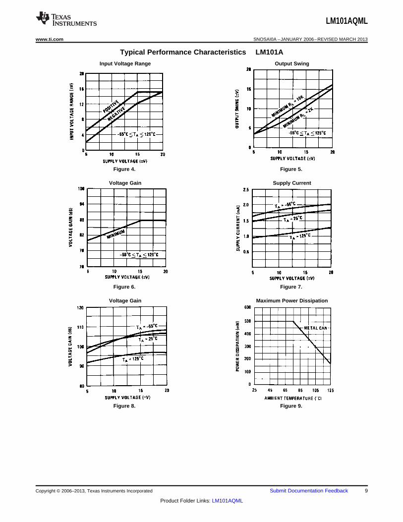
Typical Performance Characteristics LM101A
Input Voltage Range Output Swing
Figure 4. Figure 5.
Voltage Gain Supply Current
Figure 6. Figure 7.
Voltage Gain Maximum Power Dissipation
Figure 8. Figure 9.
Copyright © 2006–2013, Texas Instruments Incorporated Submit Documentation Feedback 9
Product Folder Links: LM101AQML
LM101AQML
SNOSAI0A –JANUARY 2006–REVISED MARCH 2013 www.ti.com
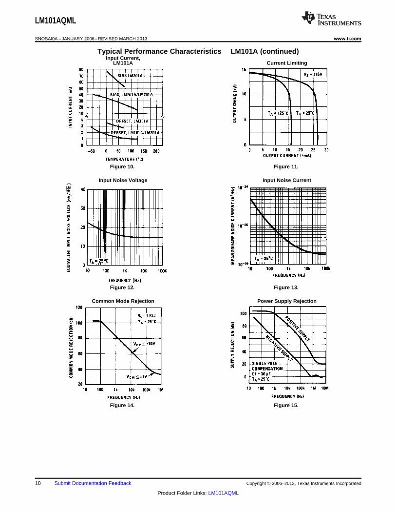
Typical Performance Characteristics LM101A (continued)Input Current,
LM101A Current Limiting
Figure 10. Figure 11.
Input Noise Voltage Input Noise Current
Figure 12. Figure 13.
Common Mode Rejection Power Supply Rejection
Figure 14. Figure 15.
10 Submit Documentation Feedback Copyright © 2006–2013, Texas Instruments Incorporated
Product Folder Links: LM101AQML
LM101AQML
www.ti.com SNOSAI0A –JANUARY 2006–REVISED MARCH 2013
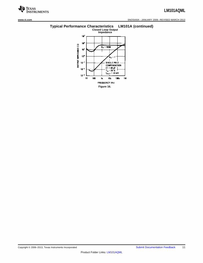
Typical Performance Characteristics LM101A (continued)Closed Loop Output
Impedance
Figure 16.
Copyright © 2006–2013, Texas Instruments Incorporated Submit Documentation Feedback 11
Product Folder Links: LM101AQML
LM101AQML
SNOSAI0A –JANUARY 2006–REVISED MARCH 2013 www.ti.com
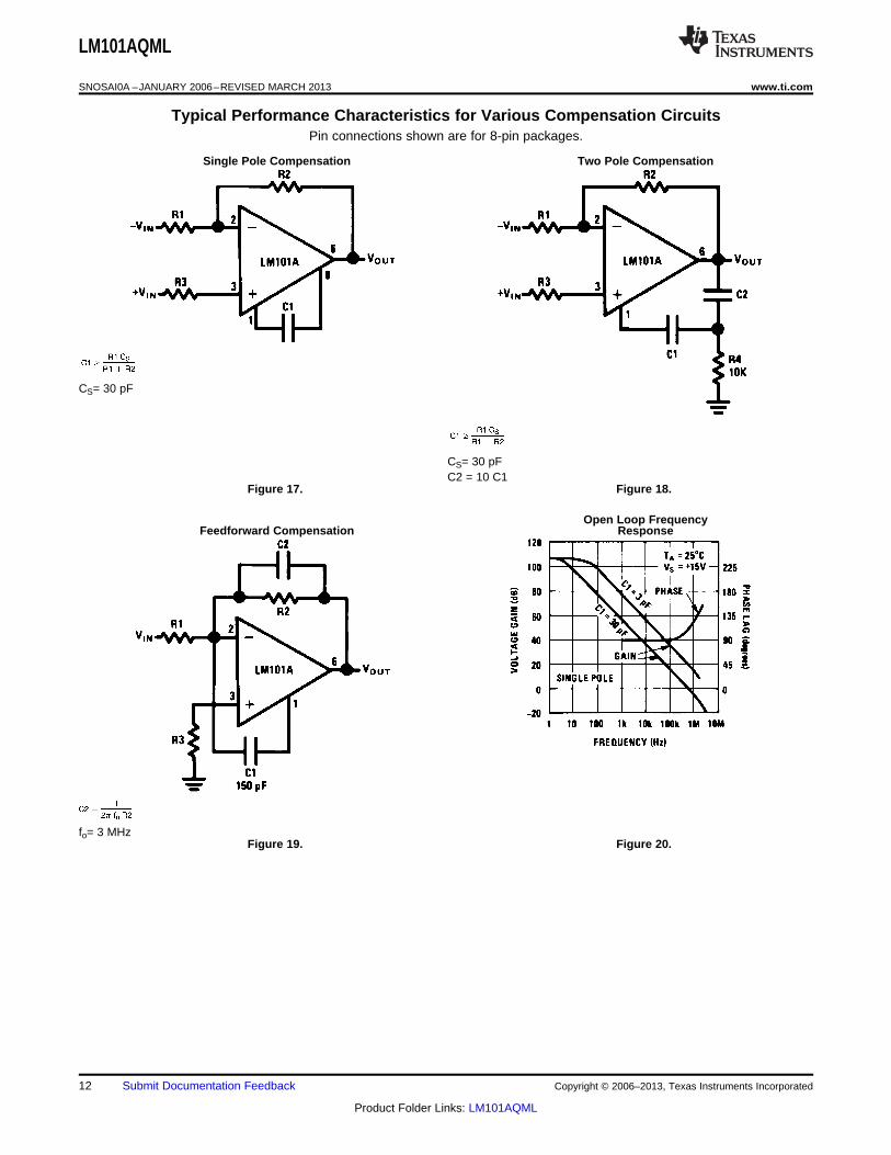
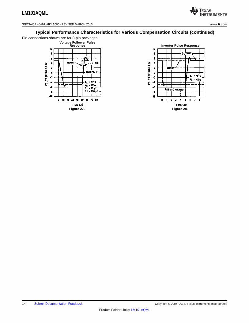
Typical Performance Characteristics for Various Compensation CircuitsPin connections shown are for 8-pin packages.
Single Pole Compensation Two Pole Compensation
CS= 30 pF
CS= 30 pFC2 = 10 C1
Figure 17. Figure 18.
Open Loop FrequencyFeedforward Compensation Response
fo= 3 MHzFigure 19. Figure 20.
12 Submit Documentation Feedback Copyright © 2006–2013, Texas Instruments Incorporated
Product Folder Links: LM101AQML
LM101AQML
www.ti.com SNOSAI0A –JANUARY 2006–REVISED MARCH 2013
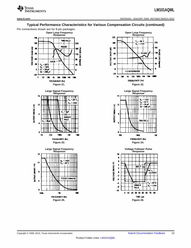
Typical Performance Characteristics for Various Compensation Circuits (continued)Pin connections shown are for 8-pin packages.
Open Loop Frequency Open Loop FrequencyResponse Response
Figure 21. Figure 22.
Large Signal Frequency Large Signal FrequencyResponse Response
Figure 23. Figure 24.
Large Signal Frequency Voltage Follower PulseResponse Response
Figure 25. Figure 26.
Copyright © 2006–2013, Texas Instruments Incorporated Submit Documentation Feedback 13
Product Folder Links: LM101AQML
LM101AQML
SNOSAI0A –JANUARY 2006–REVISED MARCH 2013 www.ti.com
Typical Performance Characteristics for Various Compensation Circuits (continued)Pin connections shown are for 8-pin packages.
Voltage Follower PulseResponse Inverter Pulse Response
Figure 27. Figure 28.
14 Submit Documentation Feedback Copyright © 2006–2013, Texas Instruments Incorporated
Product Folder Links: LM101AQML
LM101AQML
www.ti.com SNOSAI0A –JANUARY 2006–REVISED MARCH 2013
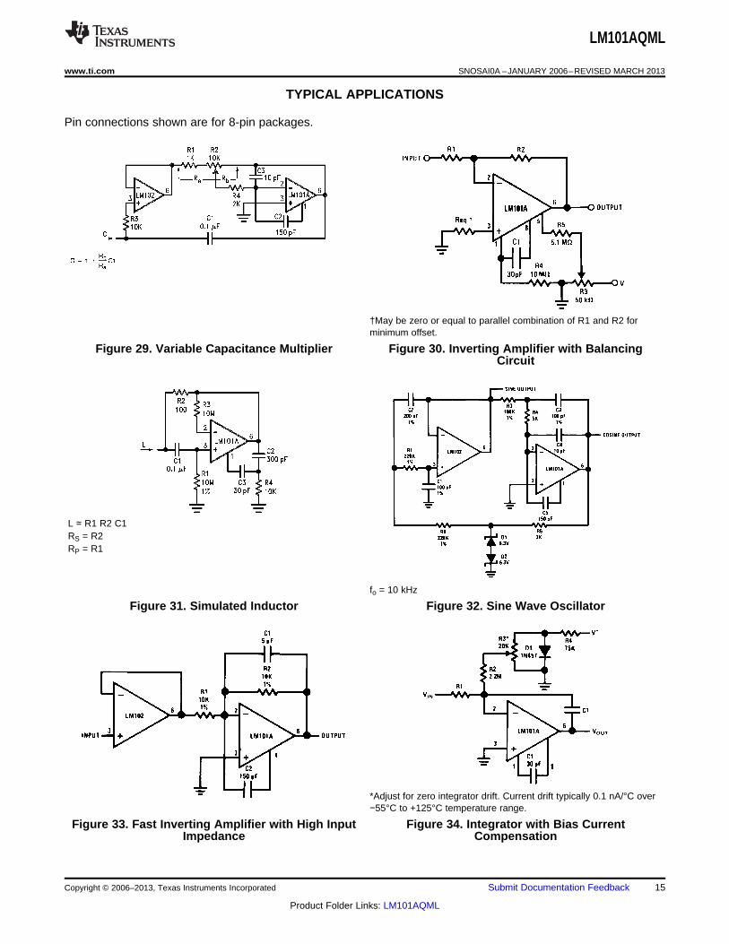
TYPICAL APPLICATIONS
Pin connections shown are for 8-pin packages.
†May be zero or equal to parallel combination of R1 and R2 forminimum offset.
Figure 29. Variable Capacitance Multiplier Figure 30. Inverting Amplifier with BalancingCircuit
L ≃ R1 R2 C1RS = R2RP = R1
fo = 10 kHz
Figure 31. Simulated Inductor Figure 32. Sine Wave Oscillator
*Adjust for zero integrator drift. Current drift typically 0.1 nA/°C over−55°C to +125°C temperature range.
Figure 33. Fast Inverting Amplifier with High Input Figure 34. Integrator with Bias CurrentImpedance Compensation
Copyright © 2006–2013, Texas Instruments Incorporated Submit Documentation Feedback 15
Product Folder Links: LM101AQML

LM101AQML
SNOSAI0A –JANUARY 2006–REVISED MARCH 2013 www.ti.com
Application Hints
*Protects input†Protects output‡Protects output—not needed when R4 is used.
Figure 35. Protecting Against Gross Fault Conditions
Figure 36. Compensating for Stray Input Capacitances or Large Feedback Resistor
Figure 37. Isolating Large Capacitive Loads
16 Submit Documentation Feedback Copyright © 2006–2013, Texas Instruments Incorporated
Product Folder Links: LM101AQML

LM101AQML
www.ti.com SNOSAI0A –JANUARY 2006–REVISED MARCH 2013
Although the LM101A is designed for trouble free operation, experience has indicated that it is wise to observecertain precautions given below to protect the devices from abnormal operating conditions. It might be pointedout that the advice given here is applicable to practically any IC op amp, although the exact reason why maydiffer with different devices.
When driving either input from a low-impedance source, a limiting resistor should be placed in series with theinput lead to limit the peak instantaneous output current of the source to something less than 100 mA. This isespecially important when the inputs go outside a piece of equipment where they could accidentally beconnected to high voltage sources. Large capacitors on the input (greater than 0.1 μF) should be treated as alow source impedance and isolated with a resistor. Low impedance sources do not cause a problem unless theiroutput voltage exceeds the supply voltage. However, the supplies go to zero when they are turned off, so theisolation is usually needed.
The output circuitry is protected against damage from shorts to ground. However, when the amplifier output isconnected to a test point, it should be isolated by a limiting resistor, as test points frequently get shorted to badplaces. Further, when the amplifer drives a load external to the equipment, it is also advisable to use some sortof limiting resistance to preclude mishaps.
Precautions should be taken to insure that the power supplies for the integrated circuit never becomereversed—even under transient conditions. With reverse voltages greater than 1V, the IC will conduct excessivecurrent, fusing internal aluminum interconnects. If there is a possibility of this happening, clamp diodes with ahigh peak current rating should be installed on the supply lines. Reversal of the voltage between V+ and V− willalways cause a problem, although reversals with respect to ground may also give difficulties in many circuits.
The minimum values given for the frequency compensation capacitor are stable only for source resistances lessthan 10 kΩ, stray capacitances on the summing junction less than 5 pF and capacitive loads smaller than 100pF. If any of these conditions are not met, it becomes necessary to overcompensate the amplifier with a largercompensation capacitor. Alternately, lead capacitors can be used in the feedback network to negate the effect ofstray capacitance and large feedback resistors or an RC network can be added to isolate capacitive loads.
Although the LM101A is relatively unaffected by supply bypassing, this cannot be ignored altogether. Generally itis necessary to bypass the supplies to ground at least once on every circuit card, and more bypass points maybe required if more than five amplifiers are used. When feed-forward compensation is employed, however, it isadvisable to bypass the supply leads of each amplifier with low inductance capacitors because of the higherfrequencies involved.
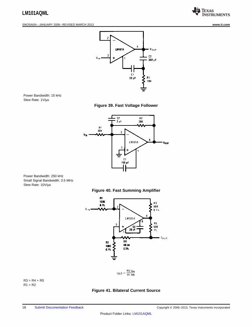
Typical Applications
Pin connections shown are for 8-pin packages.
Figure 38. Standard Compensation and Offset Balancing Circuit
Copyright © 2006–2013, Texas Instruments Incorporated Submit Documentation Feedback 17
Product Folder Links: LM101AQML
LM101AQML
SNOSAI0A –JANUARY 2006–REVISED MARCH 2013 www.ti.com
Power Bandwidth: 15 kHzSlew Rate: 1V/μs
Figure 39. Fast Voltage Follower
Power Bandwidth: 250 kHzSmall Signal Bandwiidth: 3.5 MHzSlew Rate: 10V/μs
Figure 40. Fast Summing Amplifier
R3 = R4 + R5R1 = R2
Figure 41. Bilateral Current Source
18 Submit Documentation Feedback Copyright © 2006–2013, Texas Instruments Incorporated
Product Folder Links: LM101AQML

LM101AQML
www.ti.com SNOSAI0A –JANUARY 2006–REVISED MARCH 2013
Note: Feedforward compensation can be used to make a fast full wave rectifier without a filter.
Figure 42. Fast AC/DC Converter
R1 = R4; R2 = R3
*,† Matching determines CMRR.
Figure 43. Instrumentation Amplifier
Copyright © 2006–2013, Texas Instruments Incorporated Submit Documentation Feedback 19
Product Folder Links: LM101AQML
LM101AQML
SNOSAI0A –JANUARY 2006–REVISED MARCH 2013 www.ti.com
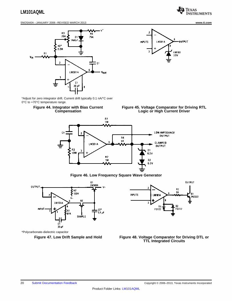
*Adjust for zero integrator drift. Current drift typically 0.1 nA/°C over0°C to +70°C temperature range.
Figure 44. Integrator with Bias Current Figure 45. Voltage Comparator for Driving RTLCompensation Logic or High Current Driver
Figure 46. Low Frequency Square Wave Generator
*Polycarbonate-dielectric capacitor
Figure 47. Low Drift Sample and Hold Figure 48. Voltage Comparator for Driving DTL orTTL Integrated Circuits
20 Submit Documentation Feedback Copyright © 2006–2013, Texas Instruments Incorporated
Product Folder Links: LM101AQML

LM101AQML
www.ti.com SNOSAI0A –JANUARY 2006–REVISED MARCH 2013
REVISION HISTORY SECTION
Date Revision Section Originator ChangesReleased
01/05/06 A New Release to corporate format L. Lytle 2 MDS datasheets converted into one Corp.datasheet format. MNLM101A-X Rev 0A0 andMRLM101A-X-RH rev 1C2 MDS datasheets willbe archived.
03/20/13 A All - Changed layout of National Data Sheet to TIformat
Copyright © 2006–2013, Texas Instruments Incorporated Submit Documentation Feedback 21
Product Folder Links: LM101AQML
PACKAGE OPTION ADDENDUM
www.ti.com 7-Oct-2021
Addendum-Page 1
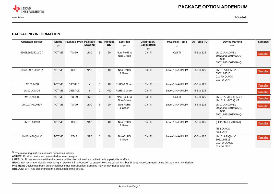
PACKAGING INFORMATION
Orderable Device Status(1)
Package Type PackageDrawing
Pins PackageQty
Eco Plan(2)
Lead finish/Ball material
(6)
MSL Peak Temp(3)
Op Temp (°C) Device Marking(4/5)
Samples
5962L9951501VGA ACTIVE TO-99 LMC 8 20 Non-RoHS &Non-Green
Call TI Call TI -55 to 125 LM101AHLQMLV5962L9951501VGA Q ACO5962L9951501VGA Q >T
5962L9951501VPA ACTIVE CDIP NAB 8 40 Non-RoHS& Green
Call TI Level-1-NA-UNLIM -55 to 125 LM101AJLQMLV5962L9951501VPA Q ACO01VPA Q >T
LM101 MDR ACTIVE DIESALE Y 0 40 RoHS & Green Call TI Level-1-NA-UNLIM -55 to 125
LM101A MD8 ACTIVE DIESALE Y 0 400 RoHS & Green Call TI Level-1-NA-UNLIM -55 to 125
LM101AH/883 ACTIVE TO-99 LMC 8 20 Non-RoHS &Non-Green
Call TI Call TI -55 to 125 LM101AH/883 Q ACOLM101AH/883 Q >T
LM101AHLQMLV ACTIVE TO-99 LMC 8 20 Non-RoHS& Green
Call TI Level-1-NA-UNLIM -55 to 125 LM101AHLQMLV5962L9951501VGA Q ACO5962L9951501VGA Q >T
LM101AJ/883 ACTIVE CDIP NAB 8 40 Non-RoHS& Green
Call TI Level-1-NA-UNLIM -55 to 125 (LF412MJ, LM101AJ) /883 Q ACO/883 Q >T
LM101AJLQMLV ACTIVE CDIP NAB 8 40 Non-RoHS& Green
Call TI Level-1-NA-UNLIM -55 to 125 LM101AJLQMLV5962L9951501VPA Q ACO01VPA Q >T
(1) The marketing status values are defined as follows:ACTIVE: Product device recommended for new designs.LIFEBUY: TI has announced that the device will be discontinued, and a lifetime-buy period is in effect.NRND: Not recommended for new designs. Device is in production to support existing customers, but TI does not recommend using this part in a new design.PREVIEW: Device has been announced but is not in production. Samples may or may not be available.OBSOLETE: TI has discontinued the production of the device.
PACKAGE OPTION ADDENDUM
www.ti.com 7-Oct-2021
Addendum-Page 2
(2) RoHS: TI defines "RoHS" to mean semiconductor products that are compliant with the current EU RoHS requirements for all 10 RoHS substances, including the requirement that RoHS substancedo not exceed 0.1% by weight in homogeneous materials. Where designed to be soldered at high temperatures, "RoHS" products are suitable for use in specified lead-free processes. TI mayreference these types of products as "Pb-Free".RoHS Exempt: TI defines "RoHS Exempt" to mean products that contain lead but are compliant with EU RoHS pursuant to a specific EU RoHS exemption.Green: TI defines "Green" to mean the content of Chlorine (Cl) and Bromine (Br) based flame retardants meet JS709B low halogen requirements of <=1000ppm threshold. Antimony trioxide basedflame retardants must also meet the <=1000ppm threshold requirement.
(3) MSL, Peak Temp. - The Moisture Sensitivity Level rating according to the JEDEC industry standard classifications, and peak solder temperature.
(4) There may be additional marking, which relates to the logo, the lot trace code information, or the environmental category on the device.
(5) Multiple Device Markings will be inside parentheses. Only one Device Marking contained in parentheses and separated by a "~" will appear on a device. If a line is indented then it is a continuationof the previous line and the two combined represent the entire Device Marking for that device.
(6) Lead finish/Ball material - Orderable Devices may have multiple material finish options. Finish options are separated by a vertical ruled line. Lead finish/Ball material values may wrap to twolines if the finish value exceeds the maximum column width.
Important Information and Disclaimer:The information provided on this page represents TI's knowledge and belief as of the date that it is provided. TI bases its knowledge and belief on informationprovided by third parties, and makes no representation or warranty as to the accuracy of such information. Efforts are underway to better integrate information from third parties. TI has taken andcontinues to take reasonable steps to provide representative and accurate information but may not have conducted destructive testing or chemical analysis on incoming materials and chemicals.TI and TI suppliers consider certain information to be proprietary, and thus CAS numbers and other limited information may not be available for release.
In no event shall TI's liability arising out of such information exceed the total purchase price of the TI part(s) at issue in this document sold by TI to Customer on an annual basis.
OTHER QUALIFIED VERSIONS OF LM101AQML, LM101AQML-SP :
• Military : LM101AQML
• Space : LM101AQML-SP
NOTE: Qualified Version Definitions:
• Military - QML certified for Military and Defense Applications
• Space - Radiation tolerant, ceramic packaging and qualified for use in Space-based application
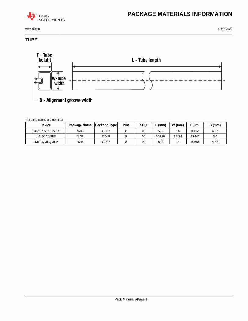
TUBE
*All dimensions are nominal
Device Package Name Package Type Pins SPQ L (mm) W (mm) T (µm) B (mm)
5962L9951501VPA NAB CDIP 8 40 502 14 10668 4.32
LM101AJ/883 NAB CDIP 8 40 506.98 15.24 13440 NA
LM101AJLQMLV NAB CDIP 8 40 502 14 10668 4.32
PACKAGE MATERIALS INFORMATION
www.ti.com 5-Jan-2022
Pack Materials-Page 1
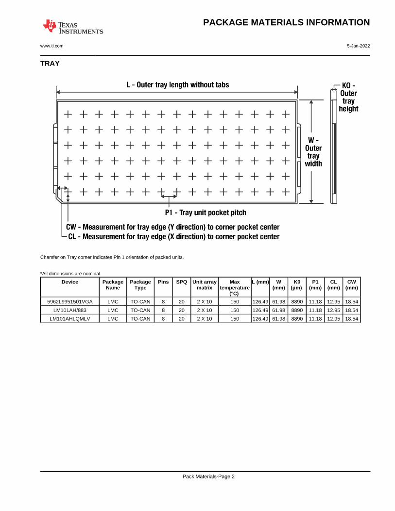
TRAY
Chamfer on Tray corner indicates Pin 1 orientation of packed units.
*All dimensions are nominal
Device PackageName
PackageType
Pins SPQ Unit arraymatrix
Maxtemperature
(°C)
L (mm) W(mm)
K0(µm)
P1(mm)
CL(mm)
CW(mm)
5962L9951501VGA LMC TO-CAN 8 20 2 X 10 150 126.49 61.98 8890 11.18 12.95 18.54
LM101AH/883 LMC TO-CAN 8 20 2 X 10 150 126.49 61.98 8890 11.18 12.95 18.54
LM101AHLQMLV LMC TO-CAN 8 20 2 X 10 150 126.49 61.98 8890 11.18 12.95 18.54
PACKAGE MATERIALS INFORMATION
www.ti.com 5-Jan-2022
Pack Materials-Page 2


MECHANICAL DATA
NAB0008A
www.ti.com
J08A (Rev M)

IMPORTANT NOTICE AND DISCLAIMERTI PROVIDES TECHNICAL AND RELIABILITY DATA (INCLUDING DATA SHEETS), DESIGN RESOURCES (INCLUDING REFERENCE DESIGNS), APPLICATION OR OTHER DESIGN ADVICE, WEB TOOLS, SAFETY INFORMATION, AND OTHER RESOURCES “AS IS” AND WITH ALL FAULTS, AND DISCLAIMS ALL WARRANTIES, EXPRESS AND IMPLIED, INCLUDING WITHOUT LIMITATION ANY IMPLIED WARRANTIES OF MERCHANTABILITY, FITNESS FOR A PARTICULAR PURPOSE OR NON-INFRINGEMENT OF THIRD PARTY INTELLECTUAL PROPERTY RIGHTS.These resources are intended for skilled developers designing with TI products. You are solely responsible for (1) selecting the appropriate TI products for your application, (2) designing, validating and testing your application, and (3) ensuring your application meets applicable standards, and any other safety, security, regulatory or other requirements.These resources are subject to change without notice. TI grants you permission to use these resources only for development of an application that uses the TI products described in the resource. Other reproduction and display of these resources is prohibited. No license is granted to any other TI intellectual property right or to any third party intellectual property right. TI disclaims responsibility for, and you will fully indemnify TI and its representatives against, any claims, damages, costs, losses, and liabilities arising out of your use of these resources.TI’s products are provided subject to TI’s Terms of Sale or other applicable terms available either on ti.com or provided in conjunction with such TI products. TI’s provision of these resources does not expand or otherwise alter TI’s applicable warranties or warranty disclaimers for TI products.TI objects to and rejects any additional or different terms you may have proposed. IMPORTANT NOTICE
Mailing Address: Texas Instruments, Post Office Box 655303, Dallas, Texas 75265Copyright © 2022, Texas Instruments Incorporated
Related Documents