On Computation and Implementation Techniques for Fast and Parallel Electromagnetic Transient Power System Simulation by Tong Duan A thesis submitted in partial fulfillment of the requirements for the degree of Doctor of Philosophy in Energy Systems Department of Electrical and Computer Engineering University of Alberta c Tong Duan, 2021

Welcome message from author
This document is posted to help you gain knowledge. Please leave a comment to let me know what you think about it! Share it to your friends and learn new things together.
Transcript
On Computation and Implementation Techniques for Fast and ParallelElectromagnetic Transient Power System Simulation
by
Tong Duan
A thesis submitted in partial fulfillment of the requirements for the degree of
Doctor of Philosophyin
Energy Systems
Department of Electrical and Computer EngineeringUniversity of Alberta
c©Tong Duan, 2021
Abstract
Electromagnetic transient (EMT) simulation is a paramount tool to study the electrical sys-
tem’s behavior and reproduce the transient waveforms prior to manufacturing and de-
ployment. However, the simulation process slows down significantly when the circuit
scale expands, and thus the fast and parallel circuit simulation techniques are required to
be studied and applied, especially for modern large-scale AC/DC grids where the MMC
converters composed of hundreds of submodules generate a large matrix. Besides, the tra-
ditional power system is evolving into a complex cyber-physical system (CPS), which also
proposes a new challenge to simulate the entire behavior of the system for quickly and
adequately evaluating the interplay between digital world and physical appliance.
To conduct fast EMT simulation for large and complex power systems, in this thesis,
the existing computation and implementation techniques are investigated and improved,
including the the multi-rate (MR) scheme, variable time-stepping (VTS) scheme, domain
decomposition (DD) scheme, and hardware based acceleration. 1) For the MR scheme,
an extended multi-rate mixed-solver (MRMS) hardware architecture is proposed for real-
time EMT emulation of hybrid AC/DC networks, which is an implementation-level work
taking advantages of the hybrid FPGA-MPSoC platform to emulate AC/DC systems in
real-time while guaranteeing the accuracy and low resource cost. 2) For the VTS scheme,
the new mathematical computational processes for the universal line model (ULM) and
universal machine (UM) model are proposed, which greatly improve the stability of the
models when the time-step changes compared to the traditional ULM and UM model.
The faster-than-real-time emulation architecture on FPGA and 4-level parallelism archi-
tecture on GPU are also proposed to conduct the VTS-based EMT simulation in parallel.
3) For the DD scheme, a novel linking-domain extraction (LDE) decomposition method
is proposed, which is a matrix-based decomposition method and can obtain the general
formulation of the inverse of the circuit conductance matrix based on the mathematical
analysis. Using the LDE method, a circuit can be simulated in parallel for the decomposed
subsystems. To fully exploit the potential of the LDE method, the hierarchical LDE decom-
ii
position method is also proposed for further applications. 4) In addition, by leveraging the
fast and parallel computing capabilities of FPGA/MPSoC/GPU hardware platforms, the
real-time co-emulation hardware architectures of EMT-based power system and commu-
nication network are proposed on both the FPGA-MPSoC and Jetson�-FPGA platforms to
accelerate the co-simulation process for AC/DC cyber-physical power systems and study
the communication-enabled global control schemes.
Although the proposed methods belong to different computation and implementation
techniques, the essential goal of those works is the same: conducting fast and parallel EMT
simulation to deal with the complexity of large-scale power systems and to significantly
accelerate the simulation process. The proposed mathematical models, computational ap-
proaches, and implementation architectures contribute to the exiting EMT simulation tech-
niques and have potential to be applied in the future EMT simulation research.
iii
Preface
The material presented in this thesis is based on original work by Tong Duan. As detailed
in the following, material from some chapters of this thesis has been published as journal
articles under the supervision of Dr. Venkata Dinavahi in concept formation and by pro-
viding comments and corrections to the article manuscript.
Chapter 2 includes the results from the following paper:
• T. Duan, Z. Shen, and V. Dinavahi, “Multi-rate mixed-solver for real-time nonlinear
electromagnetic transient emulation of AC/DC networks on FPGA-MPSoC architec-
ture,” IEEE Power Energy Technol. Syst. J., vol. 6, no. 4, pp. 183-194, Dec. 2019.
• Z. Shen, T. Duan and V. Dinavahi, “Design and implementation of real-time MPSoC-
FPGA based electromagnetic transient emulator of CIGRE DC grid for HIL applica-
tion,” IEEE Power Energy Technol. Syst. J., vol. 5, no. 3, pp. 104-116, Sept. 2018.
Chapter 3 includes the results from the following paper:
• T. Duan and V. Dinavahi, “Adaptive time-stepping universal line and machine mod-
els for real-time and faster-than-real-time hardware emulation,” IEEE Trans. Ind.
Electron., vol. 67, no. 8, pp. 6173-6182, Aug. 2020.
• T. Duan and V. Dinavahi, “Variable time-stepping parallel electromagnetic transient
simulation of hybrid AC/DC grids,” IEEE J. Emerg. Sel. Topics. Ind. Electron., vol. 2,
no. 1, pp. 90-98, Jan. 2021.
Chapter 4 includes the results from the following paper:
• T. Duan and V. Dinavahi, “A novel linking-domain extraction decomposition method
for parallel electromagnetic transient simulation of large-scale AC/DC networks,”
IEEE Trans. Power Del., early-access, pp. 1-9, May 2020.
Chapter 5 includes the results from the following papers:
iv
• T. Duan and V. Dinavahi, “Hierarchical linking-domain extraction decomposition
method for fast and parallel power system electromagnetic transient simulation,”
Submitted to IEEE Open J. Ind. Appl., pp.1-9, 2020.
Chapter 6 includes the results from the following paper:
• T. Duan, Z. Huang, and V. Dinavahi, “RTCE: real-time co-emulation framework for
EMT-based power system and communication network on FPGA-MPSoC hardware
architecture,” IEEE Trans. Smart Grid, early-access, pp. 1-10, 2020.
Chapter 7 includes the results from the following paper:
• T. Duan, T. Cheng, and V. Dinavahi, “Heterogeneous real-time co-emulation for
communication-enabled global control of AC/DC grid integrated with renewable
energy,” IEEE Open J. Ind. Electron. Soc., vol. 1, pp. 261-270, Sept. 2020.
v

To my parents and my wife,
for their unconditional support and love.
vi

Acknowledgements
I would like to express my genuine gratitude to Dr. Venkata Dinavahi, who is the super-
visor of my Ph.D. program at the University of Alberta. Without his excellent academic
proposals and patient thesis supervision, it is hard to imagine that I could overcome so
many challenges on the path of this research. His passion, patience and positive attitude
also helped me a lot during the research and daily life.
I have spent a fantastic time in the RTX-Lab, which provided wonderful hybrid hard-
ware emulation environment for my research, including the latest FPGA, MPSoC and GPU
devices. I would like to thank all the colleagues in our Lab for their kind help and sugges-
tions.
I am sincerely grateful for the unconditional support from my family: my father, Xin
Duan, my mother Guoping An, and my wife, Junqi Wang. During the study at the Univer-
sity of Alberta, they gave me a lot of psychological help that made me always feel warm
and peaceful.
The research of this thesis was supported by the China Scholarship Council, the Uni-
versity of Alberta, and NSERC. I greatly appreciate their financial support.
vii
Table of Contents
1 Introduction 11.1 Research Definition and Literature Review . . . . . . . . . . . . . . . . . . . 2
1.1.1 Multi-Rate Simulation Method . . . . . . . . . . . . . . . . . . . . . . 31.1.2 Variable Time-Stepping Simulation . . . . . . . . . . . . . . . . . . . . 31.1.3 Network Domain Decomposition . . . . . . . . . . . . . . . . . . . . 51.1.4 Co-Simulation between Communication and Power Systems . . . . 61.1.5 GPU, FPGA and SoC . . . . . . . . . . . . . . . . . . . . . . . . . . . . 6
1.2 Research Objectives . . . . . . . . . . . . . . . . . . . . . . . . . . . . . . . . . 81.3 Summary of Contributions . . . . . . . . . . . . . . . . . . . . . . . . . . . . . 91.4 Thesis Outline . . . . . . . . . . . . . . . . . . . . . . . . . . . . . . . . . . . . 12
2 Multi-Rate Mixed-Solver for Real-Time Nonlinear Electromagnetic Transient Em-ulation on FPGA-MPSoC Architecture 152.1 Proposed Multi-Rate Mixed-Solver for EMT Simulation . . . . . . . . . . . . 152.2 Comprehensive Real-Time Emulator Implementation . . . . . . . . . . . . . 192.3 Results and Verification . . . . . . . . . . . . . . . . . . . . . . . . . . . . . . 23
2.3.1 Hardware Resource Utilization and Latency . . . . . . . . . . . . . . 232.3.2 Real-Time Emulation Results . . . . . . . . . . . . . . . . . . . . . . . 25
2.4 Summary . . . . . . . . . . . . . . . . . . . . . . . . . . . . . . . . . . . . . . . 27
3 Variable Time-Stepping Universal Line and Machine Models and Implementa-tion on FPGA and GPU Platforms 283.1 Universal Transmission Line Model Computation . . . . . . . . . . . . . . . 283.2 Universal Machine Model Computation . . . . . . . . . . . . . . . . . . . . . 323.3 Time-Step Configuration and Control Scheme . . . . . . . . . . . . . . . . . . 343.4 Real-Time FPGA-Based Implementation . . . . . . . . . . . . . . . . . . . . . 36
3.4.1 Hardware Implementation . . . . . . . . . . . . . . . . . . . . . . . . 363.4.2 Latency and Hardware Resource Utilization . . . . . . . . . . . . . . 38
3.5 4-Level Parallel GPU-Based Implementation . . . . . . . . . . . . . . . . . . 393.5.1 GPU-Based VTS Simulation Architecture . . . . . . . . . . . . . . . . 393.5.2 GPU-Based Parallel Implementation . . . . . . . . . . . . . . . . . . . 41
3.6 Results and Verification . . . . . . . . . . . . . . . . . . . . . . . . . . . . . . 44
viii
3.6.1 Verification of the ULM Model . . . . . . . . . . . . . . . . . . . . . . 443.6.2 Real-Time Emulation Results of IEEE 39-Bus System on FPGA . . . . 443.6.3 Latency and Speed-Up of AC/DC Grid on GPU . . . . . . . . . . . . 47
3.7 Summary . . . . . . . . . . . . . . . . . . . . . . . . . . . . . . . . . . . . . . . 48
4 Linking-Domain Extraction Decomposition Method for Parallel ElectromagneticTransient Simulation of AC/DC Networks 494.1 Schur Complement Method . . . . . . . . . . . . . . . . . . . . . . . . . . . . 494.2 Proposed Linking-Domain Extraction based Decomposition Method . . . . 51
4.2.1 LDE Matrix Decomposition . . . . . . . . . . . . . . . . . . . . . . . . 514.2.2 Mathematical Analysis over LDM . . . . . . . . . . . . . . . . . . . . 524.2.3 Inverse Matrix of the Sum of LDM and DBM . . . . . . . . . . . . . . 564.2.4 Parallel Computation Using LDE . . . . . . . . . . . . . . . . . . . . . 574.2.5 Advantages and Limitations of LDE . . . . . . . . . . . . . . . . . . . 574.2.6 Optimal Decomposition based on LDE . . . . . . . . . . . . . . . . . 59
4.3 Simulation Results and Speed-Up . . . . . . . . . . . . . . . . . . . . . . . . . 594.3.1 Simple Demonstration Case . . . . . . . . . . . . . . . . . . . . . . . . 604.3.2 Speed-Up of Matrix Equation Solution on FPGA . . . . . . . . . . . . 604.3.3 Large-Scale AC/DC Network Simulation on GPU . . . . . . . . . . . 62
4.4 Summary . . . . . . . . . . . . . . . . . . . . . . . . . . . . . . . . . . . . . . . 64
5 Hierarchical Linking-Domain Extraction Decomposition Method for Fast and Par-allel Power System Electromagnetic Transient Simulation 655.1 Introduction . . . . . . . . . . . . . . . . . . . . . . . . . . . . . . . . . . . . . 665.2 Improved Linking-Domain Extraction based Decomposition Method . . . . 67
5.2.1 LDE Matrix Decomposition . . . . . . . . . . . . . . . . . . . . . . . . 675.2.2 Improved LDE Computation Procedure . . . . . . . . . . . . . . . . . 68
5.3 Hierarchical LDE Method . . . . . . . . . . . . . . . . . . . . . . . . . . . . . 695.3.1 Multi-Level LDE Decomposition . . . . . . . . . . . . . . . . . . . . . 695.3.2 Computational Complexity Analysis of Hierarchical LDE . . . . . . 705.3.3 Specific Decomposition Principles . . . . . . . . . . . . . . . . . . . . 73
5.4 CPU-Based Sequential and GPU-Based Parallel Implementation . . . . . . . 745.4.1 Sequential and Parallel Configuration . . . . . . . . . . . . . . . . . . 745.4.2 Test System Decomposition . . . . . . . . . . . . . . . . . . . . . . . . 75
5.5 Simulation Results and Verification . . . . . . . . . . . . . . . . . . . . . . . . 775.5.1 Speed-Up of GPU-Based Parallel H-LDE Computation . . . . . . . . 775.5.2 Speed-Up of CPU-Based Sequential H-LDE Computation . . . . . . 79
5.6 Summary . . . . . . . . . . . . . . . . . . . . . . . . . . . . . . . . . . . . . . . 81
ix
6 Real-Time Co-Emulation Framework for EMT-Based Power System and Commu-nication Network on FPGA-MPSoC Hardware Architecture 826.1 Introduction . . . . . . . . . . . . . . . . . . . . . . . . . . . . . . . . . . . . . 836.2 Co-simulation Background . . . . . . . . . . . . . . . . . . . . . . . . . . . . 85
6.2.1 Power System Simulation . . . . . . . . . . . . . . . . . . . . . . . . . 856.2.2 Communication Network Simulation . . . . . . . . . . . . . . . . . . 866.2.3 Co-Simulation . . . . . . . . . . . . . . . . . . . . . . . . . . . . . . . . 87
6.3 Proposed Real-Time Co-Emulation (RTCE) Framework . . . . . . . . . . . . 886.3.1 Motivation . . . . . . . . . . . . . . . . . . . . . . . . . . . . . . . . . . 886.3.2 RTCE Hardware Architecture . . . . . . . . . . . . . . . . . . . . . . . 88
6.4 Hardware Implementation of RTCE . . . . . . . . . . . . . . . . . . . . . . . 916.4.1 Multi-Board EMT Emulation . . . . . . . . . . . . . . . . . . . . . . . 926.4.2 Communication Protocol and Implementation . . . . . . . . . . . . . 93
6.5 Real-Time Emulation Results and Verification . . . . . . . . . . . . . . . . . . 956.5.1 Processing Delay and Hardware Resource Cost . . . . . . . . . . . . 956.5.2 Case Study 1: Overcurrent of Load . . . . . . . . . . . . . . . . . . . . 966.5.3 Case Study 2: Communication Link Failure . . . . . . . . . . . . . . . 97
6.6 Summary . . . . . . . . . . . . . . . . . . . . . . . . . . . . . . . . . . . . . . . 98
7 Heterogeneous Real-Time Co-Emulation for Communication-Enabled Global Con-trol of AC/DC Grid Integrated with Renewable Energy 997.1 Introduction . . . . . . . . . . . . . . . . . . . . . . . . . . . . . . . . . . . . . 1007.2 ICT-Enabled Hybrid AC/DC Grid . . . . . . . . . . . . . . . . . . . . . . . . 101
7.2.1 Hybrid AC/DC Power System . . . . . . . . . . . . . . . . . . . . . . 1017.2.2 Communication Network . . . . . . . . . . . . . . . . . . . . . . . . . 1027.2.3 ICT-Enabled Power System Equipment . . . . . . . . . . . . . . . . . 103
7.3 Heterogenous Real-Time Co-Emulation Architecture on Multiple Jetson�-FPGA Platform . . . . . . . . . . . . . . . . . . . . . . . . . . . . . . . . . . . 1037.3.1 Co-Emulation Architecture . . . . . . . . . . . . . . . . . . . . . . . . 1047.3.2 Hybrid AC/DC Grid EMT Emulation . . . . . . . . . . . . . . . . . . 1057.3.3 Communication Network Emulation . . . . . . . . . . . . . . . . . . 105
7.4 Hardware Implementation of Test System . . . . . . . . . . . . . . . . . . . . 1067.4.1 Heterogeneous Co-Emulator Hardware Resources and Set-Up . . . . 1067.4.2 FPGA Implementation . . . . . . . . . . . . . . . . . . . . . . . . . . . 1077.4.3 Jetson� Implementation . . . . . . . . . . . . . . . . . . . . . . . . . . 109
7.5 Real-Time Hardware Emulation Results for Communication-Enabled GlobalControl . . . . . . . . . . . . . . . . . . . . . . . . . . . . . . . . . . . . . . . . 1117.5.1 Case Study 1: Power Overflow Protection . . . . . . . . . . . . . . . . 1127.5.2 Case Study 2: DC Fault Protection . . . . . . . . . . . . . . . . . . . . 113
7.6 Summary . . . . . . . . . . . . . . . . . . . . . . . . . . . . . . . . . . . . . . . 115
x
8 Conclusions and Future Work 1168.1 Contributions of This Thesis . . . . . . . . . . . . . . . . . . . . . . . . . . . . 1178.2 Applications of the Proposed Works . . . . . . . . . . . . . . . . . . . . . . . 1188.3 Directions for Future Work . . . . . . . . . . . . . . . . . . . . . . . . . . . . . 118
Bibliography 120
xi
List of Tables
2.1 Hardware Resource Utilization of the Case Study . . . . . . . . . . . . . . . 242.2 Processing Latency of Communication and Subsystems . . . . . . . . . . . . 24
3.1 Demonstration of FTRT . . . . . . . . . . . . . . . . . . . . . . . . . . . . . . . 373.2 Processing Latency of Different Subsystems . . . . . . . . . . . . . . . . . . . 383.3 Hardware Resource Utilization of the Case Study . . . . . . . . . . . . . . . 383.4 Application of Dynamic Parallelism and Cores Used in Each Level . . . . . 423.5 Execution Time and Speed-up of Different Methods for 10s Simulation . . . 47
4.1 Execution Time and Speed-up of Different Decompositions for One Cycle(16.67ms) Simulation on GPU . . . . . . . . . . . . . . . . . . . . . . . . . . . 63
5.1 Computational Latency of 5000 Steps with Constant Matrix . . . . . . . . . . 805.2 Computational Latency (ms) of 5000 Steps with Changeable Matrix . . . . . 81
6.1 Hardware Resource Consumption of the Case Study . . . . . . . . . . . . . . 95
7.1 FPGA Hardware Resource Consumption of the Test System . . . . . . . . . 109
xii
List of Figures
1.1 Illustration of GPU dynamic parallelism. . . . . . . . . . . . . . . . . . . . . 71.2 Contributions of the proposed research and structure of this thesis. . . . . . 10
2.1 Decomposing a network into separated pure linear and nonlinear network. 162.2 Illustration of the multi-rate mixed-solver simulation. . . . . . . . . . . . . 182.3 Data-flow in the proposed multi-rate mixed-solver. . . . . . . . . . . . . . . 202.4 Topology of the AC/DC grid test case. . . . . . . . . . . . . . . . . . . . . . 212.5 Hardware emulation of the case study on two FPGA boards and one MPSoC
board. . . . . . . . . . . . . . . . . . . . . . . . . . . . . . . . . . . . . . . . . 212.6 Steady-state operation of converters. (a) DC voltage at 3-terminals; (b) Power
flow change operation of multi-converters. . . . . . . . . . . . . . . . . . . . 252.7 Lightning transient results. (a)∼(c) PSCAD/EMTDC� results with 10, 20μs
time-step and MRMS results without surge arresters deployed; (d) Resultswith surge arresters installed. . . . . . . . . . . . . . . . . . . . . . . . . . . . 26
3.1 Equivalent circuit of the ULM. . . . . . . . . . . . . . . . . . . . . . . . . . . 293.2 Illustration for the process-reversed model for the ULM. . . . . . . . . . . . 313.3 Equivalent circuit for the universal machine model. . . . . . . . . . . . . . . 333.4 TSA-based variable time-stepping control scheme: (a) global scheme, (b)
local scheme. . . . . . . . . . . . . . . . . . . . . . . . . . . . . . . . . . . . . 343.5 Example of synchronization between TSAs. . . . . . . . . . . . . . . . . . . 353.6 Test system and the hardware emulation on two interfaced FPGA boards. . 363.7 GPU-based VTS simulation: dynamic parallelism based simulation on GPUs.
. . . . . . . . . . . . . . . . . . . . . . . . . . . . . . . . . . . . . . . . . . . . 393.8 Topology of the AC/DC grid test case with time-step areas (TSAs). . . . . . 403.9 GPU implementation: (a) detailed parallel processing on GPU; (b) parallel
computing for MMC and ULM. . . . . . . . . . . . . . . . . . . . . . . . . . 423.10 Waveforms under time-step change operation: (a) traditional ULM model;
(b) proposed process-reversed ULM model. . . . . . . . . . . . . . . . . . . 433.11 Lightning transient results of i14−4 and vbus36. (a) PSCAD results with 10us
fixed time-step; (b)(c) FPGA-based emulator with 10us and 20us time-steps;(d) FPGA-based emulator with VTS. . . . . . . . . . . . . . . . . . . . . . . . 45
xiii
3.12 Demonstration of FTRT results. (a) Real-time results in VTS; (b) Results ofFTRT2 mode in VTS. . . . . . . . . . . . . . . . . . . . . . . . . . . . . . . . . 46
4.1 Example of matrix decomposition: (a) Schur decomposition method; (b)Proposed LDE method. . . . . . . . . . . . . . . . . . . . . . . . . . . . . . . 50
4.2 Example of multiple linking-domain matrices: (a) linking-domain matrixdecomposition; (b)(c) C and Λ matrix construction. . . . . . . . . . . . . . . 56
4.3 Example of two decomposed subsystems: (a) subsystem connection; (b) ma-trix decomposition. . . . . . . . . . . . . . . . . . . . . . . . . . . . . . . . . . 58
4.4 Simple demonstration case: (a) two connected subsystems (SS1 and SS2)and their equivalent circuits; (b) corresponding linking-domain matrix, Cand Λ matrix. . . . . . . . . . . . . . . . . . . . . . . . . . . . . . . . . . . . . 60
4.5 Test circuits: (a) IEEE 39-bus test system; (b) hybrid AC/DC grid; (c) de-composition of each phase circuit of MMC. . . . . . . . . . . . . . . . . . . . 61
4.6 IEEE 39-bus execution time comparison between the GJ, SC, and LDE methodunder varying number of decomposed subsystems on the FPGA. . . . . . . 61
5.1 Example of LDE decomposition of two subsystems: (a) decomposition of G;(b) Λ matrix; (c) transformation matrix C. . . . . . . . . . . . . . . . . . . . . 67
5.2 Demonstration of hierarchical LDE decomposition. . . . . . . . . . . . . . . 715.3 Recursive complexity analysis of the hierarchical LDE decomposition. . . . 725.4 Diagram of the IEEE 118-Bus test power system. . . . . . . . . . . . . . . . . 745.5 Topology partitioning of the IEEE 118-Bus test power system using the 4-
level LDE decomposition. . . . . . . . . . . . . . . . . . . . . . . . . . . . . . 765.6 Assembling process for inverting the block matrices of the first-level decom-
position with a 4-level H-LDE decomposition. . . . . . . . . . . . . . . . . . 765.7 GPU-based computational time comparison between the SC, O-LDE and H-
LDE method under different numbers of decomposed subsystems and dif-ferent decomposition levels (Latencies of 5000 time-steps of matrix equationsolution). . . . . . . . . . . . . . . . . . . . . . . . . . . . . . . . . . . . . . . 78
6.1 Example of interaction between power system and communication networksimulation. . . . . . . . . . . . . . . . . . . . . . . . . . . . . . . . . . . . . . 87
6.2 Demonstration of real-time co-emulation (RTCE) architecture on FPGA-MPSoCplatform. . . . . . . . . . . . . . . . . . . . . . . . . . . . . . . . . . . . . . . . 89
6.3 Example of co-emulating a cyber-physical system on multi-board hardwareplatform. . . . . . . . . . . . . . . . . . . . . . . . . . . . . . . . . . . . . . . . 91
6.4 Illustration of detailed block design on a single FPGA/MPSoC board. . . . 946.5 Overcurrent fault case study: (a) active power of load at Bus 7; (b) total load
current at Bus 7; (c) voltage of Bus 7. . . . . . . . . . . . . . . . . . . . . . . . 97
xiv
6.6 Communication link failure case study: (a) active power of load at Bus 7; (b)total load current at Bus 7. . . . . . . . . . . . . . . . . . . . . . . . . . . . . . 98
7.1 Hybrid AC/DC test power system used in this work. . . . . . . . . . . . . . 1027.2 Top level architecture of the heterogeneous co-emulation hardware architec-
ture on the multiple Jetson�-FPGA platform. . . . . . . . . . . . . . . . . . 1047.3 Hardware setup for the heterogeneous co-emulator. . . . . . . . . . . . . . . 1077.4 The ICT-enabled PD-SPWM MMC control scheme. . . . . . . . . . . . . . . 1107.5 Demonstration of interaction between power system emulation and com-
munication network simulation. . . . . . . . . . . . . . . . . . . . . . . . . . 1107.6 Power overflow case: a) comparison of the power flowing to Bus36 and
Bus38 with 55ms, 250ms response delay and without protection; b-c) com-parison of phasor magnitude of the current flowing to Bus36 and Bus38 andbus voltages with 55ms and 250ms response delay. . . . . . . . . . . . . . . 112
7.7 DC fault protection case: (a-b) power flowing to different buses with andwithout subsequent protection; (c-d) positive, negative pole voltage and DCvoltage of converter Bb-A1 and Bb-C2 with and without subsequent protec-tion. . . . . . . . . . . . . . . . . . . . . . . . . . . . . . . . . . . . . . . . . . 114
xv
List of Acronyms
APU Application Processing UnitATP Alternative Transients ProgramAVM Average Value ModelAXI Advanced eXtensible InterfaceBE Backward EulerBLM Bergeron Line ModelBRAM Block Random Access MemoryCFM Curve-Fitting ModelCPS Cyber-Physical SystemCPU Central Processing UnitDBM Diagonal Block MatrixDD Domain DecompositionDDR4 Double Data Rate Fourth-generationDIDT di/dtDMA Direct Memory AccessDP Dynamic ParallelismDSP Digital Signal Processing (Processor)DVDT dv/dtEMT Electro-Magnetic TransientFDLM Frequency-Dependent Line ModelFE Forward EulerFF Flip-FlopFIFO First-In First-OutFPGA Field-Programmable Gate ArrayFTRT Faster-Than-Real-TimeFTS Fixed Time-StepGJ Gauss-JordanGPU Graphics Processing UnitGT Gigabit TransceiverH-LDE Hierarchical Linking-Domain ExtractionHBSM Half-Bridge Sub-ModuleHIL Hardware-In-the-LoopHLS High-Level SynthesisHVDC High Voltage Direct CurrentI/O Input/OutputICT Information and Communication TechniqueIGBT Insulated Gate Bipolar TransistorIP Internet Protocol
xvi
KCL Kirchhoff’s Current LawKVL Kirchhoff’s Voltage LawLDE Linking-Domain ExtractionLDM Linking-Domain MatrixLIM Latency Insertion MethodLSS Linear Subsystem SolverLTE Local Truncation ErrorLUT Look-Up TablelwIP light weight Internet ProtocolMAC Media Access ControllerMMC Modular Multi-Level ConverterMPSoC Multi-Processor System-on-ChipMR Multi-RateMRMS Multi-Rate Mixed-SolverMTDC Multi-Terminal DCN-R Newton-RaphsonNSS Nonlinear Subsystem SolverPCIe Peripheral Component Interconnect expressPCS Physical Coding SublayerPD Phase-DispositionPDC Phasor Data ConcentratorPL Programmable Logic, Piecewise LinearizationPMU Phasor Measurement UnitPS Processing SystemPWM Pulse Width ModulationQSFP Quad Small Form-Factor PluggableRAM Random Access MemoryRTCE Real-Time Co-EmulationSC Schur ComplementSDK Software Development KitSFP Small Form-Factor PluggableSG Smart GridSM Sub-ModuleSPWM Sinusoidal Pulse Width ModulationSS SubSystemSTDC Super Transient Data ConcentratorTCP Transmission Control ProtocolTDC Transient Data ConcentratorTLM Transmission Line ModelTLN Transmission-Level NetworkingTMU Transient Measurement UnitTR Trapezoidal RuleTSA Time-Step AreaTSSM Two-State Switching ModelULM Universal Line ModelUM Universal MachineVTS Variable Time-Stepping
xvii
1Introduction
Electromagnetic Transient (EMT) simulation is a paramount tool in planning, operation,design and commissioning of power systems [1–4]. In EMT simulation, the power sys-tem can be described using a set of differential equations based on Kirchhoff’s currentlaw (KCL) and voltage law (KVL) analysis, where the unknown variables of the equationsare to be solved using numerical integration schemes within each discrete time slot (so-called time-step, typically at microsecond level); if the modeled system contains nonlinearelements, iterative solution is often necessary to obtain accurate results. However, the sim-ulation process slows down significantly when the circuit scale expands: the direct matrixinversion or other algorithms such as the Gauss-Jordan elimination and LU factorizationmethod have large computational complexities, which result in a high computational la-tency for large-scale networks [5]. Therefore, the fast simulation technique is becomingone of the most important areas in the EMT simulation research, and is increasingly re-quired to be studied and applied. Besides, the traditional power system is evolving into acommunication-enabled cyber-physical system (CPS), which also proposes new challengesto conduct fast simulation for the entire system while considering the interplay betweencommunication infrastructure and power system appliance [6].
To deal with the complexity of the EMT simulation for large-scale power systems, threeexisting fast simulation techniques are commonly used: the multi-rate (MR) scheme thatuses different time-step sizes for different decomposed subsystems to balance the accuracyand computational cost; the variable time-stepping (VTS) scheme that changes the time-step size during the simulation to accelerate the process under normal conditions whileguaranteeing accuracy; and the domain decomposition (DD) scheme that decomposes alarge-scale system into small subsystems and then handles the small subsystems in par-allel. However, there is still a lot of room to improve those methods and to study how
1
Chapter 1. Introduction 2to implement those methods on practical hardware platforms such as field-programmablegate array (FPGA), multi-processor system-on-chip (MPSoC) and graphics processing unit(GPU) for acceleration.
Based on the above observations, the goal of this research is to conduct fast and paral-lel EMT simulation for complex power systems to significantly accelerate the simulationprocess by proposing new computation methods and implementation architectures:
1. In the computation level, new power equipment models with VTS and new mathe-matical methods for DD are proposed in this thesis: the new mathematical compu-tational processes of the universal line model (ULM) and universal machine (UM)model are proposed, which greatly improve the stability of the models when thetime-step changes compared to the traditional ULM and UM model; a novel linking-domain extraction (LDE) method is proposed, which is a new non-overlapping de-composition method that can compute the matrix inversion in parallel based on thefound general formula of the inverse of circuit conductance matrix. To fully exploitthe potential of LDE method, the hierarchical LDE decomposition method is furtherproposed.
2. In the implementation level, the new simulation architectures on hardware platformsare proposed: for the MR scheme, an extended multi-rate mixed-solver (MRMS)hardware architecture is proposed for real-time EMT emulation of hybrid AC/DCnetworks, which takes advantages of the hybrid FPGA-MPSoC platform to emulateAC/DC systems in real-time; for the VTS scheme, the faster-than-real-time archi-tecture on FPGA and 4-level parallel architecture on GPU are proposed to conductmassively parallel simulation with variable time-steps. In addition, the novel real-time co-emulation architectures for the power system and communication networkare also proposed and conducted on the FPGA-MPSoC platform and FPGA-Jetson�
platform respectively to accelerate the co-simulation process of cyber-physical powersystems.
The proposed mathematical models, computational approaches, and implementationarchitectures contribute to the exiting EMT simulation research and have potential to beapplied in the future EMT simulation area.
1.1 Research Definition and Literature Review
The principal objective of the proposed research is to perform fast and parallel EMT simu-lation for large-scale power systems on GPU/FPGA/MPSoC hardware architectures basedon both the existing and the proposed simulation acceleration techniques. The key aspectsof the proposed research are presented in this section.
Chapter 1. Introduction 3
1.1.1 Multi-Rate Simulation Method
In modern power systems, the high voltage AC and DC transmission networks co-exist,wherein both may contain nonlinear elements [7]. The hardware emulation of solvingnonlinear elements has been evaluated in [8], which provides the nonlinear solver for thiswork. Since iterative solution of the large-scale system may involve extremely intensivecomputation, the complete system can be decomposed into multiple smaller subsystemsby leveraging the traveling wave latencies of the widely distributed long-distance trans-mission lines. The location and the contained nonlinear elements can vary for differentsubsystems. In fact, there is no need to apply the same step-size for all subsystems [9] sincethe size of the simulation time-step is dependent on the changing rate during the transientin a certain subsystem and the accuracy requirement. For example, a small time-step (ofthe order of tens of nanoseconds) that is chosen to capture the device-level switching tran-sients of AC/DC converters results in excessive execution run time, while a relatively largetime-step chosen for modeling only the system-level transients would be obviously inef-fectual in reproducing the device transients.
Therefore, the multi-rate (MR) simulation is usually adopted to accelerate the simula-tion process and reduce computational resource consumption. In multi-rate simulation,different subsystems may apply different time-steps, and the selected time-step sizes aredetermined by the changing rate of the concerned waveforms and the accuracy require-ments [10]. In multi-rate simulation, both the iterative solver for nonlinear elements andthe conventional non-iterative solver can be applied for different subsystems, which en-ables applying iterative schemes locally to reduce the computational effort. Different fromthe variable time-stepping simulation [11] that changes the time-step over the simula-tion time, in multi-rate simulation the time-steps of different subsystems are fixed, whichshould be evaluated and configured by users properly in advance to the simulation begin.
1.1.2 Variable Time-Stepping Simulation
Most real-time simulators as well as off-line EMT simulators such as the PSCAD/EMTDC�
[12], ATP [13], EMTP-RV [14], PSpice [15] and HSPICE [16] use a fixed time-step (FTS) toproceed the simulation; however, it may be not an efficient approach when the time con-stants of the power equipment in a system are widely varying and do not change veryfrequently. For example, a large time-step is usually enough to show the waveforms undernormal steady-state conditions, but a small time-step is required when the fast transientshappen. Although the variable time-stepping (VTS) method that changes the time-stepduring simulation according to accuracy requirements has been adopted in the Saber [17]simulator, it is purely targeting on the device-level simulation of power electronics. To ac-celerate the power simulation process without losing accuracy, the VTS method has beenstudied and applied in power system simulation over the past years [11, 18–24].
In modern power systems the AC and DC grids are interconnected, wherein linear and
Chapter 1. Introduction 4
nonlinear elements co-exist. In such a system, measuring the system perturbation is theprerequisite to determine the time-step change and control scheme. In this work, differentmethods are applied to estimate the accuracy:
(1) Linear Equipment: It is easy to find the solution for linear elements even with variabletime-steps because the network conductance matrix only depends on the history items attn−1. The local truncation error (LTE) is usually used to estimate the accuracy of the solvedvariable x, given by [25]:
LTE(tn) ≈ Cp+1Δtp+1n (p+ 1)! g[tn, ..., tn−1−p] (1.1)
where Cp+1 is the error constant of a specific discretization method, p is the order, andg[tn−1, ..., tn−1−k] can be calculated step-by-step:
g(tn−1) = xn−1 (1.2)
g[tn−1, ..., tn−k] =g[tn−1, ..., tn−k+1]− g[tn−2, ..., tn−k]
tn−1 − tn−k(1.3)
(2) Nonlinear Equipment: Finding xn for nonlinear equipment requires solving the non-linear system using an iterative approach. The standard method is to first use an explicitmethod or interpolation polynomial (called the predictor) to get a candidate value of xn,and then use it as the initial solution to apply Newton’s iterative method for the implicitintegrator (called the corrector) until convergence is achieved. For the predictor, the inter-polation polynomial is commonly used:
x(0)n = xn−1 +p∑
k=1
[k∏
j=1
(tn − tn−j)]g[tn−1, ..., tn−1−k] (1.4)
Then the LTE can be estimated by comparing the initial solution x0n and final solutionxn [25]:
LTE(tn) ≈ Cp+1
1− Cp+1(xn − x0n) (1.5)
(3) AC/DC Converter. Although a modular multilevel converter (MMC) is also madeup of linear and nonlinear equipment such as the IGBT switches, capacitors and induc-tors, the LTE method may not be suitable for MMC because it is hard to find which statevariable is most representative among the thousands of switches and capacitors and sixarm inductors. Thus for the system-level simulation, the differential value dv/dt (DVDT)or di/dt (DIDT) of DC voltage or current is computed to measure the system disturbanceand determine the time-step change [23]; for the device-level simulation, the switchingoperation is used to trigger the time-step change.
Since the universal line model (ULM) [26] and universal machine (UM) [27] modelserve a wide range of transmission lines and rotating machines, they are required to beproperly modeled for variable time-stepping (VTS) EMT simulation. Although the vari-able time-stepping model for the traveling-wave line model has already been studied
Chapter 1. Introduction 5
in [18, 20], to the best of our knowledge, the VTS models for ULM and UM have not beenderived. The work [21, 22] applied the variable time-stepping simulation in frequency-domain, but the frequency-domain line model was simplified without involving the con-volution process and both works simulated the system in software but not in hardware forreal-time. The work [24] implemented the variable time-stepping simulation in real-timewith nonlinear systems such as the power electronic converters and surge arresters; how-ever, all of the power equipment models use the same time-step size, which is not suitablefor the VTS simulation of large-scale systems. Although the system decomposition canbe applied to use different time-steps for different subsystems [10], the time-step of eachsubsystem also changes in the VTS simulation; thus how to deal with data exchange andsynchronization between subsystems with variable time-steps remains to be discussed.
1.1.3 Network Domain Decomposition
To deal with the complexity of simulating large-scale systems, network domain decompo-sition [28] is a commonly-used method that splits a large network into small subsystemsand simulates them in parallel. One main challenge of using domain decomposition is howto uncouple the inter-connected subsystems, which leads to two representative categoriesof decomposition methods [29]: overlapping domain decomposition and non-overlappingdomain decomposition. In overlapping domain decomposition, the basic logic is to al-locate the overlapping domain between two connected subsystems (multiple subsystemshave the same procedure) into both subsystems, so that each subsystem can compute thevalues of the overlapping domain simultaneously. However, to obtain the correct valuesof the overlapping domain, data exchange and iteration are required to guarantee the dif-ference of results between the two subsystems are smaller than a predetermined threshold.In addition, when the number of decomposed subsystems increases, the convergence timewill become much longer, and thus the overlapping domain decomposition method is notthe scope of this work.
In non-overlapping domain decomposition, the decomposed subsystems have no over-lapping domains thus they could be simulated in parallel while not requiring iteration tosynchronize the connected subsystems. For the non-overlapping domain decomposition,the most widely-used methods are the transmission line modeling (TLM) [30, 31], latencyinsertion method (LIM) [32, 33] and Schur Complement (SC) method [29]. The TLM andLIM methods are latency-based decomposition methods, which leverage the transmissionlatency between two ends of a line or the latency produced by the LC circuits to decomposethe network. Both methods need to consider the simulation time-step size. For example, ifthe transmission latency of a line is smaller than the time-step size, then the two ends of theline could not be calculated simultaneously. For networks where transmission lines do notexist, the SC method is most commonly used [34, 35], which is a matrix-based decomposi-tion method. It moves all the overlapping area in the network conductance matrix to the
Chapter 1. Introduction 6
bottom right; then the remaining parts are diagonal block matrices that can be handled inparallel. However, the SC method could not obtain the network matrix inversion directly,thus the corresponding procedures need to be executed in each time-step. In addition, theefficiency reduces quickly when the overlapping domain expands.
1.1.4 Co-Simulation between Communication and Power Systems
With the development of cyber physical power systems, the co-simulation between powersystems and communication networks is becoming a hot topic in EMT simulation. Var-ious co-simulation frameworks for interacting communication and power domains havebeen proposed in the recent past since the first interface for the EMTDC/PSCAD� simu-lator [36] to integrate an agent-based distributed application into the simulation was de-veloped. Most of these works are not to design a complete simulator that could finishsimulation in one package but are targeting interfacing two existing simulators in each do-main [37–42], because there are already various mature power system and network simula-tors to use. For example, EMTDC/PSCAD�, DigSilent�, PowerWorld�, and OpenDSS�
etc are widely used in power system simulation; while NS-2/NS-3, OMNeT++, OPNETand NeSSi have been successfully used in network development and evaluation. Unfor-tunately, there does not have existing interfaces for data exchange between simulators ofthe two domains due to the different working principles. Thus the main concern of exist-ing co-simulator frameworks is to properly handle data exchange and synchronization forrelated events in both domains at run-time [6, 43]. However, the performance of software-based simulators is relatively low compared with actual power and network devices evenwithout taking the data exchange and synchronization time between two simulators intoaccount. It is therefore difficult to simulate and test the adequacy of manufactured pro-tection and control equipment responding to damage and upset by transient in real-time.To the best of our knowledge, the real-time co-simulator implemented on FPGA/MPSoCboard has not been studied. Instead of interfacing the software based simulators, FPGAenables flexible programmability and highly paralleled computing, which is able to cap-ture and response to the system change quickly in both power system and communicationnetwork domains.
1.1.5 GPU, FPGA and SoC
For large-scale power systems, the parallel simulation is often required to accelerate thesimulation process, which is usually achieved on the parallel computing architectures:the graphics processing unit (GPU), field-programmable gate array (FPGA) and multi-processor system-on-chip (MPSoC). The GPU device is composed of a huge amount ofprocessing cores, which enables the generation of numerous grids, blocks, and threadsand parallel simulation of large-scale power systems [44–47]. FPGA provides numeroushardware and rich I/O resources, which has been used in both industry and academia for
Chapter 1. Introduction 7
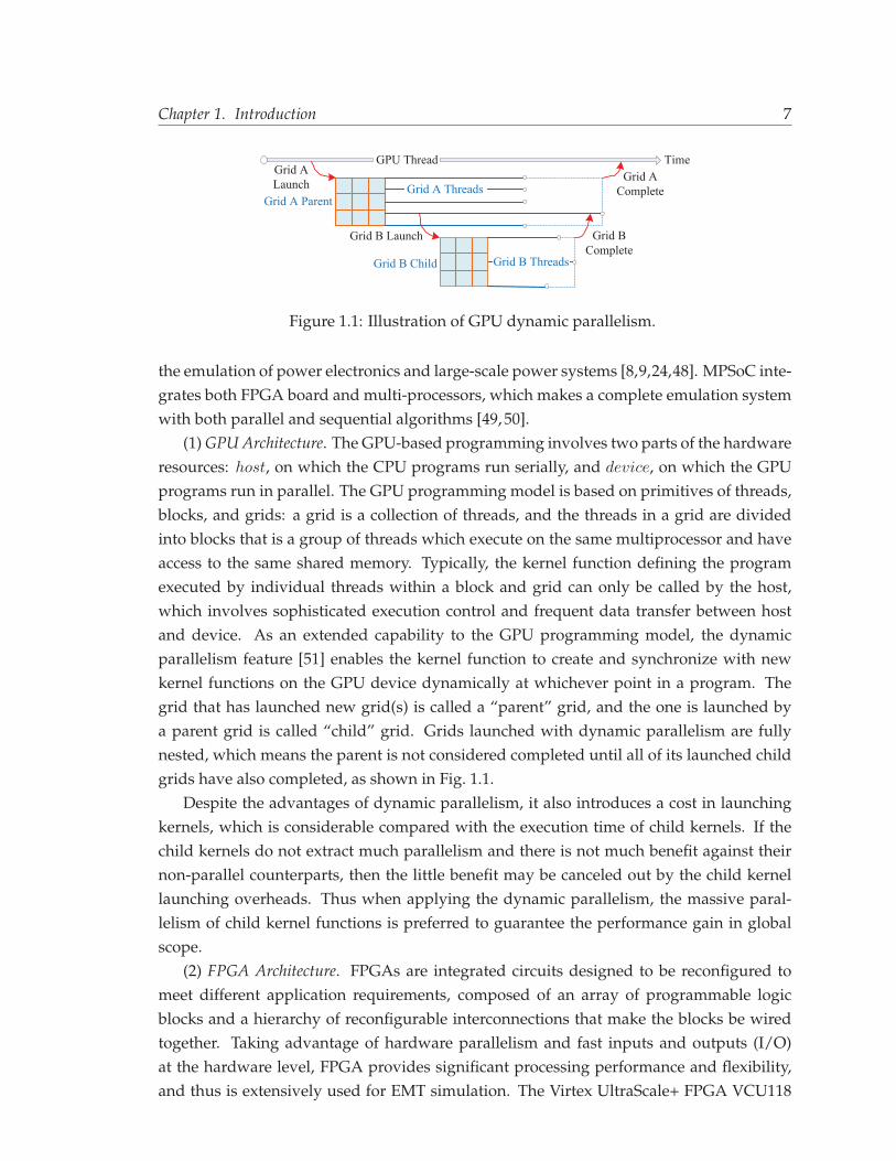
GPU Thread TimeGrid ALaunch
Grid A Parent
Grid B Child
Grid A Threads
Grid B Launch
Grid AComplete
Grid B Threads
Grid BComplete
Figure 1.1: Illustration of GPU dynamic parallelism.
the emulation of power electronics and large-scale power systems [8,9,24,48]. MPSoC inte-grates both FPGA board and multi-processors, which makes a complete emulation systemwith both parallel and sequential algorithms [49, 50].
(1) GPU Architecture. The GPU-based programming involves two parts of the hardwareresources: host, on which the CPU programs run serially, and device, on which the GPUprograms run in parallel. The GPU programming model is based on primitives of threads,blocks, and grids: a grid is a collection of threads, and the threads in a grid are dividedinto blocks that is a group of threads which execute on the same multiprocessor and haveaccess to the same shared memory. Typically, the kernel function defining the programexecuted by individual threads within a block and grid can only be called by the host,which involves sophisticated execution control and frequent data transfer between hostand device. As an extended capability to the GPU programming model, the dynamicparallelism feature [51] enables the kernel function to create and synchronize with newkernel functions on the GPU device dynamically at whichever point in a program. Thegrid that has launched new grid(s) is called a “parent” grid, and the one is launched bya parent grid is called “child” grid. Grids launched with dynamic parallelism are fullynested, which means the parent is not considered completed until all of its launched childgrids have also completed, as shown in Fig. 1.1.
Despite the advantages of dynamic parallelism, it also introduces a cost in launchingkernels, which is considerable compared with the execution time of child kernels. If thechild kernels do not extract much parallelism and there is not much benefit against theirnon-parallel counterparts, then the little benefit may be canceled out by the child kernellaunching overheads. Thus when applying the dynamic parallelism, the massive paral-lelism of child kernel functions is preferred to guarantee the performance gain in globalscope.
(2) FPGA Architecture. FPGAs are integrated circuits designed to be reconfigured tomeet different application requirements, composed of an array of programmable logicblocks and a hierarchy of reconfigurable interconnections that make the blocks be wiredtogether. Taking advantage of hardware parallelism and fast inputs and outputs (I/O)at the hardware level, FPGA provides significant processing performance and flexibility,and thus is extensively used for EMT simulation. The Virtex UltraScale+ FPGA VCU118
Chapter 1. Introduction 8
board [52] used in this research contains both highly programmable UltraScale XCVU9Pdevice and rich external resources such as block RAMs, transceivers, DSP slices and I/Opins, which enables the usage of iterative method and the detailed models applied in thiswork. High-level synthesis (HLS), provided by Xilinx�, translates C/C++ language toHDL with highly paralleled hardware structure [53]. HLS supports the arbitrary dataprecision and provides abundant directives for optimization, such as loop unroll, arraypartition, pipelining, etc. Since C/C++ language has much higher abstraction than HDL,the coding effort is substantially reduced.
(3) MPSoC Architecture. The MPSoC itself integrates the programmable logic (PL) re-source and the ARM� multi-core processor system (PS) on the same chip. Compared withthe solution of using discrete CPU and FPGA on different boards, the single-chip solutionprovides substantially higher communication bandwidth and coherence between the PSand the PL. The improved overall performance of both sequential and parallel computingby using FPGA-MPSoC platform enables the usage of the iterative method and the de-tailed models applied in this work. The Zynq ZCU102 board [54] used in this research isfeatured with a quad-core ARM� Cortex-A53, dual-core Cortex-R5 real-time processors,and a Mail-400 MP2 graphics processing unit (GPU) based on programmable logic fabric.The PS communicate with the PL using high-bandwidth Advanced eXtensible Interface(AXI) channels, enabling low-latency data exchange. Using such an architecture, sequen-tial computing and configurations can be moved into PS that can achieve high clock fre-quency, while parallel computing can be processed in PL that can achieve high parallelism.
1.2 Research Objectives
The motivation of this thesis is consistent with one of the most concerned aspects in thegeneral research of EMT simulation area, which is to accelerate the simulation process forcomplex power systems while guaranteeing reasonable accuracies. The new technologiesof hardware platforms and emerging cyber-physical power systems also require the cor-responding developments of the simulation architectures. Such challenges come from thehigher demand of simulation efficiencies for the modern grid, which requires the solutionsfrom both the computation methods and hardware implementation architectures.
The major tasks and specific research objectives for this work are listed as following:
• Multi-Rate Mixed-Solver Architecture for AC/DC Network EmulationIn modern AC/DC systems, linear and nonlinear elements co-exist, while differentpower equipment has widely different time constants. To simulate such a power sys-tem, the multi-rate scheme requires to be applied. The task of this work is to designa multi-rate real-time emulation architecture with linear and nonlinear solvers de-ployed, called the “multi-rate mixed-solver” architecture, to emulate the AC/DCnetwork in real-time. The emulation is expected to be conducted on the hybrid
Chapter 1. Introduction 9
FPGA-MPSoC hardware platform to fully utilize the advantages in both parallel andserial computing.
• Variable Time-Stepping Universal Line and Machine Models and ImplementationIn the research of variable time-stepping power equipment modeling, the universalline model (ULM) and universal machine (UM) models with variable time-steps havenot been investigated. Due to the convolution computation in ULM and exciter ofUM, the instability problem when the time-step changes should be addressed. Thegoal of this work is to propose a stable ULM and UM model no matter how the time-step changes. Besides, the parallel VTS simulation architecture is quite different fromthe FTS architecture, which should also be proposed and implemented on both theFPGA and GPU platform.
• Linking-Domain Extraction Based Domain Decomposition MethodDifferent from the latency-based decomposition method, the matrix-based non-overl-apping domain decomposition methods still have a lot of room to be studied. Thetraditional Schur complement decomposition method is not efficient when the num-ber of decomposed subsystems increases. The task of this work is to study the specialfeatures of the conductance matrix of the traditional power systems, and to find thegeneral formulation of the matrix inversion and solve the matrix equations in paral-lel. The simulation and verification is expected to be conducted on FPGA, GPU andCPU for different test systems and application contexts.
• Co-Emulation Hardware Architecture for Cyber-Physical SystemsThe emerging cyber-physical power system combines the physical layer with the in-formation and communication techniques (ICT), which propose a new challenge tothe fast co-simulation of power system and communication networks. The influ-ence of communication behaviours between the smart meters, phasor measurementunit, controller and controllable devices should be evaluated practically and pre-cisely. The goal of this work is to implement the real-time co-emulator (RTCE) onhybrid FPGA-MPSoC hardware platform and FPGA-Jetson� platform instead of in-terfacing the software-based simulators, which aims to leverage the hardware basedsimulator that is able to response to the system change quickly in both power systemand communication network domains.
1.3 Summary of Contributions
The major contributions of this work can be summarized into two aspects: computationalmethod and implementation architecture, as shown in Fig. 1.2. The proposed computa-tional methods are based on the mathematical analysis and discoveries; while the pro-
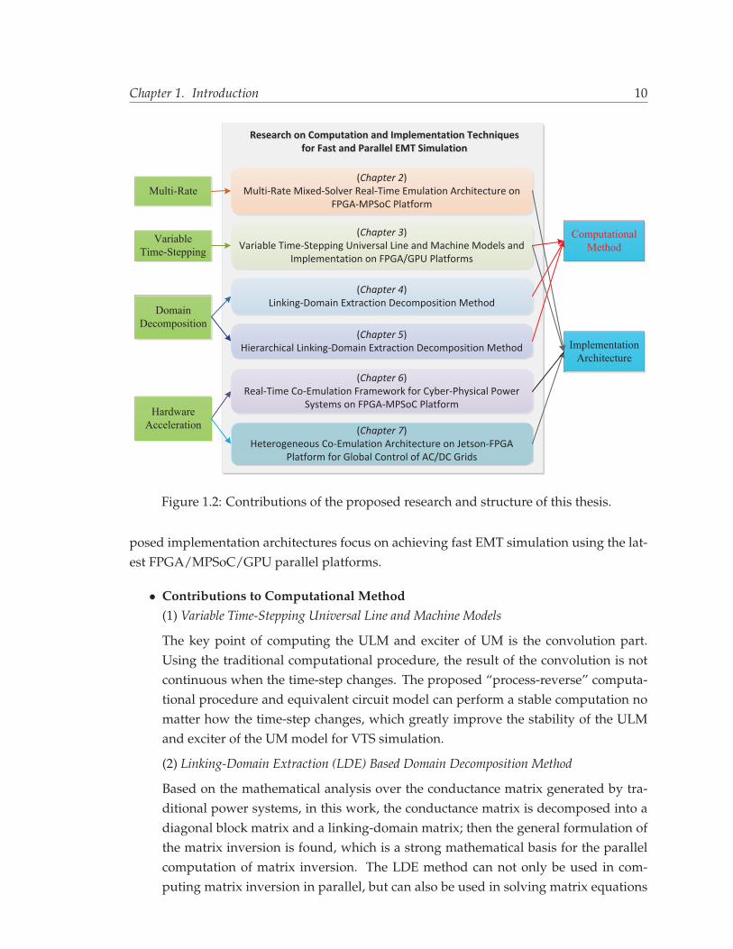
Chapter 1. Introduction 10
Multi-Rate
VariableTime-Stepping
DomainDecomposition
(Chapter 2)Multi-Rate Mixed-Solver Real-Time Emulation Architecture on
FPGA-MPSoC Platform
(Chapter 3)Variable Time-Stepping Universal Line and Machine Models and
Implementation on FPGA/GPU Platforms
(Chapter 4)Linking-Domain Extraction Decomposition Method
(Chapter 5)Hierarchical Linking-Domain Extraction Decomposition Method
(Chapter 6)Real-Time Co-Emulation Framework for Cyber-Physical Power
Systems on FPGA-MPSoC Platform
(Chapter 7)Heterogeneous Co-Emulation Architecture on Jetson-FPGA
Platform for Global Control of AC/DC Grids
Research on Computation and Implementation Techniquesfor Fast and Parallel EMT Simulation
Research on Computation and Implementation Techniques for Fast and Parallel EMT Simulation
ComputationalMethod
ImplementationArchitecture
HardwareAcceleration
Figure 1.2: Contributions of the proposed research and structure of this thesis.
posed implementation architectures focus on achieving fast EMT simulation using the lat-est FPGA/MPSoC/GPU parallel platforms.
• Contributions to Computational Method(1) Variable Time-Stepping Universal Line and Machine Models
The key point of computing the ULM and exciter of UM is the convolution part.Using the traditional computational procedure, the result of the convolution is notcontinuous when the time-step changes. The proposed “process-reverse” computa-tional procedure and equivalent circuit model can perform a stable computation nomatter how the time-step changes, which greatly improve the stability of the ULMand exciter of the UM model for VTS simulation.
(2) Linking-Domain Extraction (LDE) Based Domain Decomposition Method
Based on the mathematical analysis over the conductance matrix generated by tra-ditional power systems, in this work, the conductance matrix is decomposed into adiagonal block matrix and a linking-domain matrix; then the general formulation ofthe matrix inversion is found, which is a strong mathematical basis for the parallelcomputation of matrix inversion. The LDE method can not only be used in com-puting matrix inversion in parallel, but can also be used in solving matrix equations
Chapter 1. Introduction 11
with several advantages over the traditional Schur complement method.
(3) Hierarchical LDE Decomposition Method
The original LDE method is inefficient in both the computational procedure and stor-age cost. To proposed hierarchical LDE (H-LDE) method is an all-round improve-ment over the original LDE method, which eliminates the necessity of computing theentire conductance matrix inversion and uses a multi-level decomposition to acceler-ate the process of inverting the decomposed block matrices. The H-LDE method caneven achieve lower computation latencies than the sparse LU based solvers within acertain power system scale.
• Contributions to Implementation Architecture(1) Real-Time Multi-Rate Mixed-Solver Emulation Architecture on FPGA-MPSoC Platform
To simulate AC/DC power systems in real-time, the multi-rate mixed-solver emu-lation architecture is proposed. By moving the MMC control tasks into the ARM�
based processor system of MPSoC board, the MMC model can be computed in real-time; by re-using the linear solvers when the nonlinear solvers are working, the hard-ware resource costs can be reduced a lot; by allocating the large system into multipleFPGA boards, the multi-board solution is exploited and the fast data exchange be-tween different boards is achieved via the Xilinx� Aurora core.
(2) Faster-than-Real-Time Emulation Architecture on FPGA and 4-level Parallel SimulationArchitecture on GPU for VTS Simulation
The parallel VTS simulation architecture is quite different from the FTS architec-ture due to the synchronization between decomposed subsystems. In this work, theFPGA-based and GPU-based parallel simulation architectures are proposed for VTSsimulation. Through elaborate configuration to the time-step sizes of different sub-systems, the “faster-than-real-time” mode is achieved on FPGA; using the dynamicparallelism features and hierarchical decomposition, the massively parallel VTS sim-ulation is achieved on GPU.
(3) Co-Emulation Hardware Architecture for Cyber-Physical Systems
The existing software-based co-simulation platforms are facing the difficulties of ac-celerating the simulation process due to the large overhead of data exchange and syn-chronization. In the proposed real-time co-emulation (RTCE) framework on FPGA-MPSoC based hardware architecture, the real-time discrete-time based power systemEMT emulation and the discrete-event based communication network emulation canbe achieved. The data exchange between two domains is handled within each boardwith an extremely low latency, which is sufficiently fast for real-time interaction.In the proposed heterogeneous Jetson�-FPGA based co-emulation architecture, thecommunication-enabled global control schemes are studied for AC/DC cyber phys-ical power systems.
Chapter 1. Introduction 12
1.4 Thesis Outline
This thesis consists of eight chapters. The subsequent chapters shown in Fig. 1.2 are out-lined as follows:
• Chapter 2This chapter proposes a novel multi-rate mixed-solver architecture for AC/DC sys-tem emulation to fully utilize the time space and optimize hardware computationresources without loss of accuracy, wherein both iterative and non-iterative solverswith different time-steps are applied to the decomposed subsystems, and the linearsolvers are reused within each time-step. The proposed solver and the complete real-time emulation system are implemented on FPGA-MPSoC platform. The real-timeresults are captured by the oscilloscope and verified with PSCAD/EMTDC� andSaberRD� for system-level and device-level performance evaluation.
• Chapter 3This chapter derives the VTS models for ULM and UM, and the proposed ULMmodel is more stable than the traditional model. Both VTS models are emulatedon the parallel and pipelined architecture of the FPGA. The proposed subsystem-based VTS scheme and the local truncation error (LTE) based time-step control en-able the large-scale systems to be simulated in real-time. The “faster-than-real-time”modes on FPGA boards, and 4-level dynamic parallelism architecture on GPU arealso proposed for variable time-stepping EMT simulation. The transient waveformsand execution time speed-ups indicate that the proposed method can extremely ac-celerate the simulation process while guaranteeing reasonable accuracy compared tothe fixed time-step based simulation.
• Chapter 4In this chapter, a novel linking-domain extraction (LDE) based decomposition methodis proposed, in which the network matrix is expressed as the sum of a linking-domainmatrix (LDM) and a diagonal block matrix (DBM) composed of multiple block ma-trices in diagonal. Through mathematical analysis over LDM, one lemma about thenature of LDM and its proof are proposed. Based on this lemma, the general formu-lation of the inverse matrix of the sum of LDM and DBM can be found using theWoodbury matrix identity, and based on the formulation the network matrix inver-sion can be directly computed in parallel to accelerate the matrix inversion process.Test systems were implemented on both the FPGA and GPU parallel architectures,and the simulation results and speed-ups over the Schur complement method andGauss-Jordan elimination demonstrate the validity and efficiency of the proposedLDE method.
• Chapter 5
Chapter 1. Introduction 13
In this chapter, a novel hierarchical LDE (H-LDE) method is proposed to further im-prove the LDE method, which leverages all the hidden features of LDE that are notexploited in the original work to perform a multi-level decomposition of power sys-tems. The LDE-based matrix equation solution computation procedure is first pro-posed to eliminate the necessity of computing the entire matrix inversion, and thenthe multi-level computation structure is proposed for fast matrix inversion of thedecomposed sub-matrices. The 4-level LDE decomposition is applied on the IEEE118-bus test power system and implemented in both sequential and parallel, whichis used to verify the validity and efficiency of the proposed H-LDE decompositionmethod. The simulation results of various benchmark test power systems show thatthe proposed H-LDE method can achieve lower computation latency than the classi-cal LU factorization and sparse KLU method within a certain system scale.
• Chapter 6This chapter proposes a novel real-time co-emulation (RTCE) framework on FPGA-MPSoC based hardware architecture for a more practical emulation of real-worldcyber-physical systems. The discrete-time based power system electromagnetic tran-sient (EMT) emulation is executed in programmable hardware units so that the tran-sient level behaviour can be captured in real-time, while the discrete-event based com-munication network emulation is modeled in abstraction-level or directly executedon the hardware PHY and network ports of the FPGA-MPSoC platform, which canperform the communication networking in real-time. The data exchange betweentwo domains is handled within each platform with an extremely low latency, whichis sufficiently fast for real-time interaction; and the multi-board scheme is deployedto practically emulate the communication between different power system areas. Thehardware resource cost and emulation latency for the test system and case studiesare evaluated to demonstrate the validity and effectiveness of the proposed RTCEframework.
• Chapter 7In this chapter, a heterogeneous hardware real-time co-emulator composed of FP-GAs, many-core GPU, and multi-core CPU devices is proposed to study the com-munication enabled global control schemes of hybrid AC/DC networks. The elec-tromagnetic transient (EMT) power system emulation is conducted on the Xilinx�
FPGA boards to provide nearly continuous instantaneous waveforms for cyber layersampling; the communication layer is simulated on the ARM� CPU cores of the em-bedded NVIDIA� Jetson platform for flexible computing and programming; and thecontrol functions for modular multi-level converters are executed on GPU cores ofthe Jetson� platform for parallel calculation. The data exchange between FPGAs andJetson� is achieved via the PCI express interface, which simulates the sampling op-eration of the AC phasor measurement unit (PMU) and DC merging unit (DC-MU).
Chapter 1. Introduction 14
The power overflow and DC fault cases are investigated to demonstrate the valid-ity and effectiveness of the proposed co-emulation hardware architecture and globalcontrol schemes.
• Chapter 8This chapter summarizes the contributions of this research and discusses the futurework for the EMT simulation study.
2Multi-Rate Mixed-Solver for Real-Time
Nonlinear Electromagnetic TransientEmulation on FPGA-MPSoC Architecture
Nonlinear phenomena widely exist in AC/DC power systems, which should be accountedfor accurately in real-time EMT simulation for obtaining precise results for hardware-in-the-loop applications. However, iterative solutions such as the Newton-Raphason methodthat can precisely obtain the results for highly nonlinear elements, are time consuming andcomputationally onerous. To fully utilize the time space and optimize hardware compu-tation resources without loss of accuracy, this chapter proposes a novel multi-rate mixed-solver hardware architecture for real-time emulation of AC/DC systems, wherein bothiterative and non-iterative solvers with different time-steps are applied to the decomposedsubsystems, and the linear solvers are reused within each time-step. The proposed solverand the complete real-time emulation system are implemented on FPGA-MPSoC platform.The real-time results are captured by the oscilloscope and verified with PSCAD/EMTDC�
for system-level performance evaluation.
2.1 Proposed Multi-Rate Mixed-Solver for EMT Simulation
In the real-time EMT simulation, the size of simulation time-step is an essential variablethat directly determines the time-step dependent parameters and influences the elementmodel selection and computational resource costs. Since the time-step requirements canvary between different subsystems, the multi-rate mixed-solver for real-time EMT simula-tion is proposed to reduce the hardware resource costs and improve the overall accuracy.
Typically, by applying the KVL and KCL to the network to be solved, the network
15
Chapter 2. Multi-Rate Mixed-Solver for Real-Time Nonlinear Electromagnetic TransientEmulation on FPGA-MPSoC Architecture 16
i1
i2
in
v1v2
vn
...
...
v1v2
vn
...
[Y ]l [G ]nlLinearNetwork
NonlinearNetwork
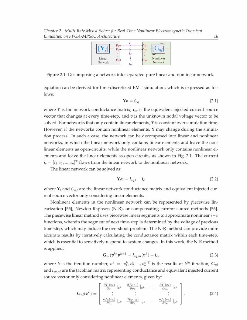
Figure 2.1: Decomposing a network into separated pure linear and nonlinear network.
equation can be derived for time-discretized EMT simulation, which is expressed as fol-lows:
Yv = ieq (2.1)
where Y is the network conductance matrix, ieq is the equivalent injected current sourcevector that changes at every time-step, and v is the unknown nodal voltage vector to besolved. For networks that only contain linear elements, Y is constant over simulation time.However, if the networks contain nonlinear elements, Y may change during the simula-tion process. In such a case, the network can be decomposed into linear and nonlinearnetworks, in which the linear network only contains linear elements and leave the non-linear elements as open-circuits, while the nonlinear network only contains nonlinear el-ements and leave the linear elements as open-circuits, as shown in Fig. 2.1. The currentic = [i1, i2, ..., in]
T flows from the linear network to the nonlinear network.The linear network can be solved as:
Ylv = ieq,l − ic (2.2)
where Yl and ieq,l are the linear network conductance matrix and equivalent injected cur-rent source vector only considering linear elements.
Nonlinear elements in the nonlinear network can be represented by piecewise lin-earization [55], Newton-Raphson (N-R), or compensating current source methods [56].The piecewise linear method uses piecewise linear segments to approximate nonlinear i−v
functions, wherein the segment of next time-step is determined by the voltage of previoustime-step, which may induce the overshoot problem. The N-R method can provide moreaccurate results by iteratively calculating the conductance matrix within each time-step,which is essential to sensitively respond to system changes. In this work, the N-R methodis applied:
Gnl(vk)vk+1 = ieq,nl(vk) + ic, (2.3)
where k is the iteration number, vk = [vk1 , vk2 , ..., v
kn]
T is the results of kth iteration, Gnl
and ieq,nl are the Jacobian matrix representing conductance and equivalent injected currentsource vector only considering nonlinear elements, given by:
Gnl(vk) =
⎡⎢⎢⎣
∂f1(v1)∂v1
|vk∂f1(v1)∂v2
|vk · · · ∂f1(v1)∂vn
|vk
......
...∂fn(vn)
∂v1|vk
∂fn(vn)∂v2
|vk · · · ∂fn(vn)∂vn
|vk
⎤⎥⎥⎦ . (2.4)
Chapter 2. Multi-Rate Mixed-Solver for Real-Time Nonlinear Electromagnetic TransientEmulation on FPGA-MPSoC Architecture 17
where the function fi(vi) represents the nonlinear i− v characteristics for node voltage vi.Then the iterative matrix equation for solving the nonlinear network can be derived from(2.2) and (2.3) by eliminating ic:
[Yl + Gnl(vk)]vk+1 = ieq,l + ieq,nl(vk) (2.5)
Since the iteration times are uncertain and the conductance matrix could be re-factorized,the N-R method could consume more time and resource than piecewise linear method.Thus, it is extremely hard to apply N-R method in large AC/DC systems where the ma-trix size is large. However, since transmission lines widely exist in AC/DC systems andthe line length is usually sufficiently long to guarantee the traveling time is longer thanthe simulation time-step, the large AC/DC network can be decomposed into m subsys-tems using the traveling-wave line model or frequency-dependent line model (FDLM), asshown below: ⎡
⎢⎢⎢⎣Y11 0 · · · 00 Y22 · · · 0...
......
0 0 · · · Ymm
⎤⎥⎥⎥⎦
⎛⎜⎜⎜⎝
vS1
vS2...
vSm
⎞⎟⎟⎟⎠ =
⎛⎜⎜⎜⎝
ieq,S1ieq,S2
...ieq,Sm
⎞⎟⎟⎟⎠ (2.6)
where Yii is the conductance matrix of subsystem Si, 1 � i � m. Assume the first ml
subsystems are linear networks, and the last mnl subsystems are nonlinear. These subsys-tems can be solved concurrently within each time-step. The linear solver only involves oneprocess of solving the matrix equations, whereas the nonlinear solver may need several it-erations of such process, which could take several times the latency of processing than thatof the linear solver. Therefore, during the processing of nonlinear solver iterations in eachtime-step, there will be much idle time for linear solver, and as a result, there will be a lotof hardware resource wasted. On the other hand, the transient behaviors of subsystemswhere transients such as lightning and switching occur need to be adequately modeledand precisely revealed, while the subsystems distant from the transients are only slightlyaffected by them and thus they do not need very small time-step to capture the systembehavior.
Based on the above observations, the multi-rate mixed-solver is proposed: to ensurehigh accuracy, both the iterative solver for nonlinear elements and the conventional non-iterative linear solver are applied for different subsystems; and to reduce computationresource consumption, the multiple time-step scheme is used and carefully designed fordifferent subsystems. The proposed multi-rate mixed-solver can be formulated as follows:
YiivΔtl(i)Si = iΔtl(i)
eq,Si , 1 � i � ml (2.7)
Yii(vk,Δtnl(i)Si )vk+1,Δtnl(i)
Si = iΔtnl(i)eq,Si (vk,Δtnl(i)
Si ), ml + 1 � i � m (2.8)
whereYii(v
k,Δtnl(i)Si ) = Yl,i + Gnl,i(v
k,Δtnl(i)Si ) (2.9)
Chapter 2. Multi-Rate Mixed-Solver for Real-Time Nonlinear Electromagnetic TransientEmulation on FPGA-MPSoC Architecture 18
NSS1:Iteration 1
NSS1:Iteration 1
Linear solverSmall time-step
NSS1:Iteration 1
...
∆ts
Time
NSS1:Iteration 1
NonlinearIterative solver
Linear solverSmall time-stepLSS 1 (S )
NSS1:Iteration 1
...
Smalltime-step
Linear solverSmall time-stepNSS1:Iteration 1
Linear solverLarge time-step
...
1S
Linear solverSmall time-step
NSS1:Iteration 1
...
∆ts
NSS1:Iteration 1
NonlinearIterative solver
Linear solverSmall time-step
NSS1:Iteration 1
...
Smalltime-step
NSS1:Iteration 1
∆tL
Largetim
e-step
Linear solverLarge time-step
NSS1:Iteration1
NSS1:Iteration2
NSS1:Iterationm
NSS1:Iterationm
NSS1:Iteration1
NSS1:Iteration2
LSS 1 (S )2S
LSS 1 (S )hS
LSS 1 (S )1S
LSS 1 (S )2S
LSS 1 (S )hS
LSS 1 (S )1L
LSS 1 (S )2L
LSS 1 (S )k-1L
LSS 1 (S )kL
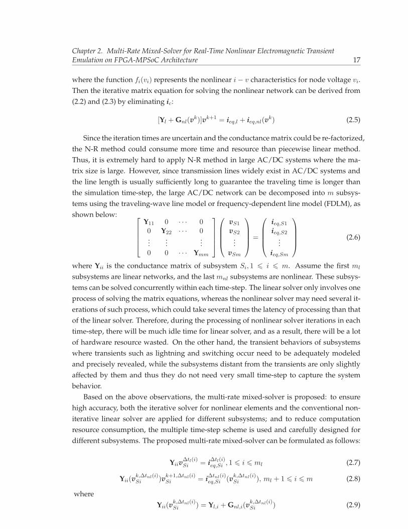
Figure 2.2: Illustration of the multi-rate mixed-solver simulation.
iΔtnl(i)eq,Si (vk,Δtnl(i)
Si ) = iΔtnl(i)eq,l,Si + iΔtnl(i)
eq,nl,Si(vk,Δtnl(i)Si ) (2.10)
Δtl(i),Δtnl(i) ∈ {Δtj |1 � j � p} (2.11)
Equation (2.11) denotes that there are p different time-steps (Δt1, ...,Δtp) applied, and sub-system Si is assigned time-step Δtl(i) or Δtnl(i) depending on linear or nonlinear systems.Equations (2.9) and (2.10) have the same form as the derived iterative matrix equation(2.5). After each time-step, the results may need to be exchanged between connected sub-systems, thus interpolation is required if the two subsystems use different time-steps. Forexample, if subsystem Si needs the results vΔtl(j)
Sj at simulation time t (t is exactly integermultiple of Δtl(i)) from subsystem Sj , then Si should interpolate the results received fromSj into the data for its own use. In this work, linear interpolation is used:
vΔtl(j)Sj |t= vΔtl(j)
Sj |t1 +t− t1Δtl(j)
(vΔtl(j)Sj |t2 −vΔtl(j)
Sj |t1), (2.12)
t1 = rounddown(t
Δtl(j))×Δtl(j) (2.13)
t2 = roundup(t
Δtl(j))×Δtl(j) (2.14)
For the case shown in Fig. 2.2 as an example, there are two time-steps applied (smalltime-step ΔtS and large time-step ΔtL). Within one small time-step, nonlinear subsystemsolvers (NSS) perform iterative calculations, while the linear subsystem solver (LSS) withsmall time-step is reused by subsystems SS
1 − SSh to fully use the time space; and within
one large time-step, linear solvers with large time-step are reused by subsystems SL1 − SL
k
and the results at the end of small time-step can be obtained by interpolation between two
Chapter 2. Multi-Rate Mixed-Solver for Real-Time Nonlinear Electromagnetic TransientEmulation on FPGA-MPSoC Architecture 19
large time-step results. After each time-step, results of the NSS and LSS with small time-step and the LSS with large time-step are outputted for display respectively and historyitems are exchanged between adjacent subsystems.
In the proposed multi-rate mixed-solver, the selection of time-step sizes and solvertypes for different subsystems should be carefully analyzed. Assume there are m subsys-tems S (S1, S2, ..., Sm), and p different rates with time-step sizes of ΔT (Δt1,Δt2, ...,Δtp) tobe selected. Other than the time-step size, reuse of the linear solver for multiple subsys-tems should also be evaluated. Let K = (K1,K2, ...,Kq) denotes the used solvers includinglinear and nonlinear solvers, then the selection can be seen as a mapping g : S �→ (ΔT,K).The principle of time-step selection is to minimize the total cost including the accuracy andhardware resource consumption while guaranteeing the accuracy requirements, which canbe formulated as follows:
minC(g) =m∑i=1
p∑j=1
q∑k=1
[αE(i, j, k) + βR(i, j, k)] · g(i, j, k) (2.15)
s.t. E(i, j, k) · g(i, j, k) � Eth,i (2.16)m∑i=1
g(i, j, k) · tk � Δtj (2.17)
where g(i, j, k) = 1 if Si uses Δtj as time-step, and is calculated by the solver Kk; andotherwise g(i, j, k) = 0. E(i, j, k) and R(i, j, k) represent the simulation error and the cor-responding resource cost respectively of subsystem Si with time-step size of Δtj usingsolver Kk, and they are both nonlinear functions of mapping g. Besides, as indicated in(2.16), E(i, j, k)g(i, j, k) should not be bigger than the pre-determined threshold error Eth,i
of subsystem Si, which means if E(i, j) is larger than Eth,i then g(i, j, k) should be equalto zero. Equation (2.17) indicates that the total calculating time of each solver selected bysubsystem Si (denoted as ti) should not exceed the selected time-step size, the summationsign means the reuse of solver is taken into consideration. α and β are scaling factors thatunify the two parts of cost. It also should be noted that the number of used solvers q isnot a pre-determined constant but a variable of which the optimal value can be solved by(2.15). However, the equations above are just the principle for time-step selection, becausethe precise function of E(i, j, k) and R(i, j, k) can only be obtained by experiment and canvary between different systems and different implementation platforms.
2.2 Comprehensive Real-Time Emulator Implementation
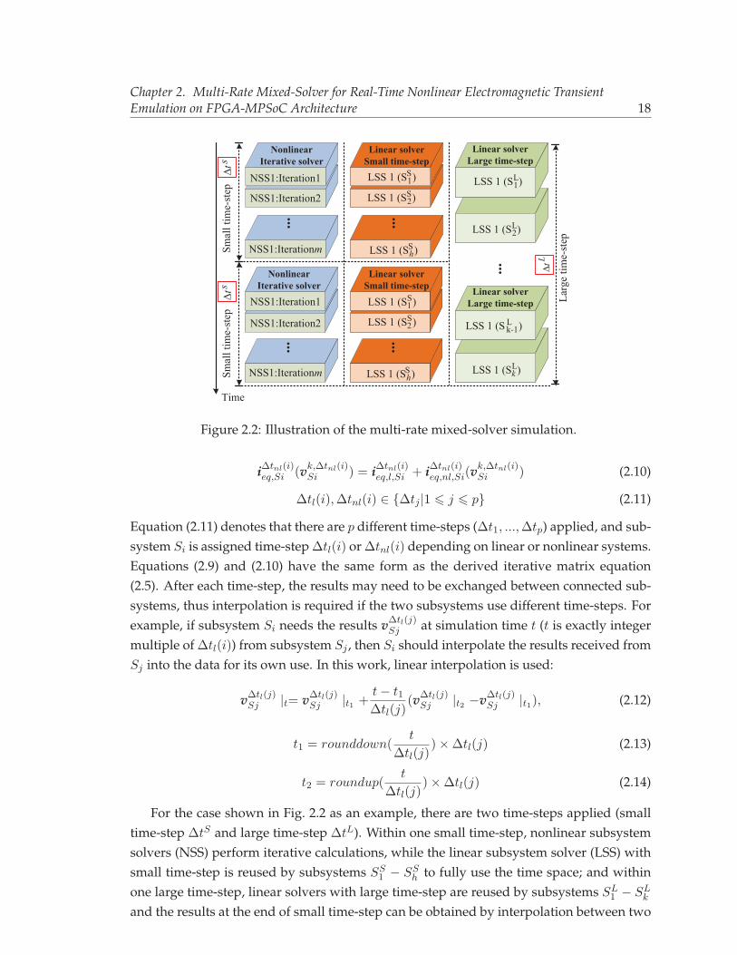
The data-flow of the MRMS simulation is illustrated in Fig. 2.3. In the example, there aretwo rates with time-step of Δt1 and Δt2, and three solvers named NSS1, LSS1 and LSS2.NSS1 is a nonlinear subsystem solver performing several iterations, after each iteration thevoltage v and conductance matrix G is updated until |(vk − vk−1)/vk| is smaller than the
Chapter 2. Multi-Rate Mixed-Solver for Real-Time Nonlinear Electromagnetic TransientEmulation on FPGA-MPSoC Architecture 20
time
LSS 1
1t
2t
Y , i v1 1 1LSS 1
v2 2 2 LSS 1v3 3 3
...vIteration 1 Iteration 2 Iteration 3
NSS 1
hist S1
S4
S2 S3hist
2tLSS 2
...
... ...
v4Y , i4 4
hist hist
S4
LSS 2v44 4
hist hist
1t
2t
3t
hist(t - )1,41hist(t - )1,41 hist(t - )1,42 hist(t - )1,43
v , G(1) (1) (2) (2)
hist hist hist hist
v , G S5
Y , i
Y , i Y , i
Figure 2.3: Data-flow in the proposed multi-rate mixed-solver.
pre-determined threshold. LSS1∼2 are linear solvers, and LSS1 is reused by subsystemsS1, S2, and S3. For simplicity, Fig. 2.3 only illustrates the data exchange between subsystemS1 and S4, and the other connections are omitted.
For thorough analysis of the proposed MRMS solver on real-time FPGA-MPSoC em-ulator, an AC/DC grid composed of two IEEE 39-bus systems [57] and a three-terminalHVDC system was chosen as the circuit topology, as shown in Fig. 2.4. In each IEEE 39-bussystem, 10 generators, 12 transformers, 19 loads and 34 transmission lines are deployed,and the two IEEE 39-bus systems are connected by three AC/DC MMC converter stationsthat are connected via two DC transmission lines. The control of converter C1 is used forDC voltage regulation, while in the converters C2/C3 the active power flow is chosen asthe controlled variable. To protect generators, transformers, cables and other devices fromovervoltages caused by lightning, short circuit, switching, etc, 6 surge arresters are alsoinstalled in the system.
The MPSoC ZCU102 board [54] used in this chapter is featured with a quad-core ARM�
Cortex-A53, dual-core Cortex-R5 real-time processors, and a Mail-400 MP2 graphics pro-cessing unit (GPU) based on programmable logic fabric. These processors (PS) communi-cate with the programmable logic (PL) using high-bandwidth Advanced eXtensible Inter-face (AXI) channels, enabling low-latency data exchange. The hybrid Virtex UltraScale+FPGA VCU118 board [52] and MPSoC ZCU102 board platform enable the usage of theiterative method and the detailed models applied.
To extend the resource capacity for simulating the large system, the multi-board so-lution is applied in this work, as shown in Fig. 2.5, there are totally three FPGA/MPSoCboards (two VCU118 boards and one ZCU102 board) used to run the study case. ZCU102board is the master board connecting with two VCU118 boards and sending instructionsto control the behavior of the other two boards. The two VCU118 boards are slave boards,which start or stop to perform simulation under the instruction of the master board. The
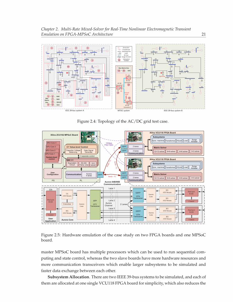
Chapter 2. Multi-Rate Mixed-Solver for Real-Time Nonlinear Electromagnetic TransientEmulation on FPGA-MPSoC Architecture 21
37
25
2
1
30
39
9 8
765
4
3110
11
12
13
15
163
1817
26
27
28 29
24
19
20
32
34 33
21 22
35
23
36
38
14
MTDC system
AC-DC Converter 2AC-DC
Converter 1
AC-DC Converter 3
40
41
42
GroundFault
37
25
2
1
30
39
9 8
765
4
3110
11
12
13
15
163
1817
26
27
28 29
24
19
20
32
34 33
21 22
35
23
36
38
14Lightning
IEEE 39-bus system A IEEE 39-bus system B
Overhead line
Generator
Load
Transformer
DC lineSurge Arrester
C1
C2
C3
1 2 3
5
4
9
6
7
81 6~ 6×67 9×98 12×12
9 11~ 3×3
11
10
MaxMatrixSize:
14~ 5×5Max Matrix Size:
12
13
14
xx Subsystem number
12
Figure 2.4: Topology of the AC/DC grid test case.
QSFP
Xilinx ZCU102 MPSoC Board
PS PL
Xilinx VCU118 FPGA Board
QSFP
QSFP
APU Core 4
APU Core 3
APU Core 2
APU Core 1
System-levelcontrol
AXI
Communication Aurora4 lanes
hist(t -
)
hist(t - )
hist(t -)
Matrix Solver
Subsystems
Sync. machine Transformer FDLM Load
Communication
2 lanes
2 lanes
UserConfiguration
C1 Value-level ControlCapacitor Voltage
BalancingGate SignalGenerate
MMC C1DC-DC
Trans. LineEquivalentCircuit
SFP
GTYTransceiver
Aurora Core
Lane 1
Lane 2
Lane 4
AuroraChannel
Lane 3
UserApplication
32b
64b
64b
Aurora 64B/66BCommmunication
2 Lanes
SurgeArrester
9×9 solver 6×6 solver 3×3 solver12×12 solver
5×5solver
3 separate control
10GbpsFiber Optic
Xilinx VCU118 FPGA Board
QSFP
QSFP
Matrix Solver
SubsystemsSync. machine Transformer FDLM Load
Communication
2 lanes
2 lanes
SurgeArrester
9×9 solver 6×6 solver 3×3 solver12×12 solver
Dual-portRAM
Control
TXAXI Stream
Correction
RXAXI Stream
AuroraLane
QSFP
GTHTransceiver
AuroraLane
RXAXI Stream
RXAXI Stream Dual-port
RAM
Control
QSFP
GTHTransceiver
AuroraLane
RXAXI Stream
RXAXI Stream Dual-port
RAM
Control
Figure 2.5: Hardware emulation of the case study on two FPGA boards and one MPSoCboard.
master MPSoC board has multiple processors which can be used to run sequential com-puting and state control, whereas the two slave boards have more hardware resources andmore communication transceivers which enable larger subsystems to be simulated andfaster data exchange between each other.
Subsystem Allocation. There are two IEEE 39-bus systems to be simulated, and each ofthem are allocated at one single VCU118 FPGA board for simplicity, which also reduces the
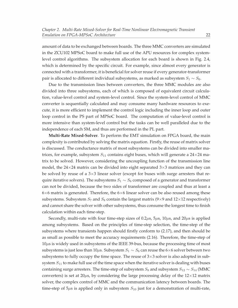
Chapter 2. Multi-Rate Mixed-Solver for Real-Time Nonlinear Electromagnetic TransientEmulation on FPGA-MPSoC Architecture 22
amount of data to be exchanged between boards. The three MMC converters are simulatedin the ZCU102 MPSoC board to make full use of the APU resources for complex system-level control algorithms. The subsystem allocation for each board is shown in Fig. 2.4,which is determined by the specific circuit. For example, since almost every generator isconnected with a transformer, it is beneficial for solver reuse if every generator-transformerpair is allocated to different individual subsystems, as marked as subsystem S1 ∼ S6.
Due to the transmission lines between converters, the three MMC modules are alsodivided into three subsystems, each of which is composed of equivalent circuit calcula-tion, value-level control and system-level control. Since the system-level control of MMCconverter is sequentially calculated and may consume many hardware resources to exe-cute, it is more efficient to implement the control logic including the inner loop and outerloop control in the PS part of MPSoC board. The computation of value-level control ismore intensive than system-level control but the tasks can be well paralleled due to theindependence of each SM, and thus are performed in the PL part.
Multi-Rate Mixed-Solver. To perform the EMT simulation on FPGA board, the maincomplexity is contributed by solving the matrix equation. Firstly, the reuse of matrix solveris discussed. The conductance matrix of most subsystems can be divided into smaller ma-trices, for example, subsystem S11 contains eight buses, which will generate a 24×24 ma-trix to be solved. However, considering the uncoupling function of the transmission linemodel, the 24×24 matrix can be divided into eight separated 3×3 matrices and they canbe solved by reuse of a 3×3 linear solver (except for buses with surge arresters that re-quire iterative solvers). The subsystems S1 ∼ S6 composed of a generator and transformercan not be divided, because the two sides of transformer are coupled and thus at least a6×6 matrix is generated. Therefore, the 6×6 linear solver can be also reused among thesesubsystems. Subsystem S7 and S8 contain the largest matrix (9×9 and 12×12 respectively)and cannot share the solver with other subsystems, thus consume the longest time to finishcalculation within each time-step.
Secondly, multi-rate with four time-step sizes of 0.2μs, 5μs, 10μs, and 20μs is appliedamong subsystems. Based on the principles of time-step selection, the time-step of thesubsystems where transients happen should firstly conform to (2.17), and then should beas small as possible to meet the accuracy requirements (2.16). Therefore, the time-step of10μs is widely used in subsystems of the IEEE 39-bus, because the processing time of mostsubsystems is just less than 10μs. Subsystem S1 ∼ S6 can reuse the 6×6 solver between twosubsystems to fully occupy the time space. The reuse of 3×3 solver is also adopted in sub-system S11 to make full use of the time space when the iterative solver is dealing with busescontaining surge arresters. The time-step of subsystem S8 and subsystem S12 ∼ S14 (MMCconverters) is set at 20μs, by considering the large processing delay of the 12×12 matrixsolver, the complex control of MMC and the communication latency between boards. Thetime-step of 5μs is applied only in subsystem S10 just for a demonstration of multi-rate,

Chapter 2. Multi-Rate Mixed-Solver for Real-Time Nonlinear Electromagnetic TransientEmulation on FPGA-MPSoC Architecture 23
because subsystem S10 has the smallest scale and matrix size. The time-step of 0.2μs isadopted for device-level simulation, and considering the limited hardware resources inthe MPSoC board only the first SM of MMC C2 is simulated in device-level to produce thedevice-level transient. The simple curve-fitting model is applied so that the device-levelbehaviours can be emulated in real-time.
Data Exchange. The history values of the two ends of a transmission line are exchangedafter each time-step and stored in a FIFO, and the FIFO shift based on the common time-step size, which is the minimum step-size for the system (5μs). For example, if the time-step of a subsystem is 10μs, then the shifted-register will shift 2 to store the data, whichmakes the same location of the memory in different subsystems store the data generatedsimultaneously.
If the two ends of a line are computed in different boards, the communication betweeninterfaced boards should be designed. To enable high-speed communication between thethree boards, lightweight communication protocol should be used instead of the com-mon TCP/IP protocol that involves too much time cost during connection establishment.Xilinx� provides a scalable link-layer communication protocol, Aurora [58], which is openand supported by different type of transceivers such as GTY and GTH transceivers. TheXilinx� aurora core can automatically initialize and maintain the channel, and the AXI-4user interface enables users to conveniently generate and receive data without consideringthe transmission details and handling transmission states. The communication part of theimplementation is shown in Fig. 2.5, the three boards are connected with each other viatwo lanes. After channel establishment, the aurora core reads data from the RAM and a64b AXI-4 stream based data is generated by combining the 32b user data and 32b addresstogether. The 32b address is used to identify the user data and put it into the right addressof the RAM after receiving.
2.3 Results and Verification
The example test case described above is emulated on the three FPGA/MPSoC boards andthe results are compared with PSCAD/EMTDC� and SaberRD� to show the effectivenessof the proposed multi-rate mixed-solver. The APU cores of MPSoC board run at 1.2GHz,while the clock frequency of FPGA boards is set at 100 MHz.
2.3.1 Hardware Resource Utilization and Latency
According to the hardware implementation details and subsystem allocation describedabove, the system-level hardware resource consumption and time-step size are presentedin Table 2.1, in which VCU118-1 represents the version that does not reuse the mixed-solver, and VCU118-2 represents the optimized cost by reusing the linear solvers. Since thetwo VCU118 boards have nearly the same cost by simulating the same size of circuit topol-
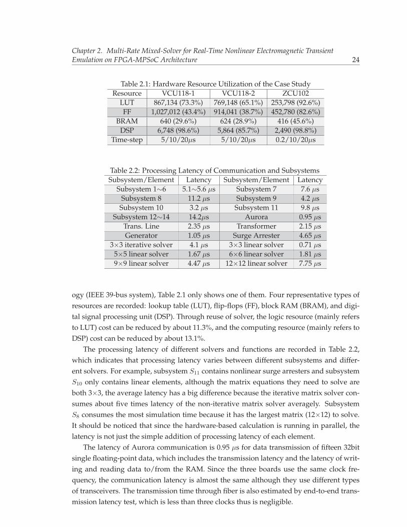
Chapter 2. Multi-Rate Mixed-Solver for Real-Time Nonlinear Electromagnetic TransientEmulation on FPGA-MPSoC Architecture 24
Table 2.1: Hardware Resource Utilization of the Case StudyResource VCU118-1 VCU118-2 ZCU102
LUT 867,134 (73.3%) 769,148 (65.1%) 253,798 (92.6%)FF 1,027,012 (43.4%) 914,041 (38.7%) 452,780 (82.6%)
BRAM 640 (29.6%) 624 (28.9%) 416 (45.6%)DSP 6,748 (98.6%) 5,864 (85.7%) 2,490 (98.8%)
Time-step 5/10/20μs 5/10/20μs 0.2/10/20μs
Table 2.2: Processing Latency of Communication and SubsystemsSubsystem/Element Latency Subsystem/Element Latency
Subsystem 1∼6 5.1∼5.6 μs Subsystem 7 7.6 μsSubsystem 8 11.2 μs Subsystem 9 4.2 μsSubsystem 10 3.2 μs Subsystem 11 9.8 μs
Subsystem 12∼14 14.2μs Aurora 0.95 μsTrans. Line 2.35 μs Transformer 2.15 μsGenerator 1.05 μs Surge Arrester 4.65 μs
3×3 iterative solver 4.1 μs 3×3 linear solver 0.71 μs5×5 linear solver 1.67 μs 6×6 linear solver 1.81 μs9×9 linear solver 4.47 μs 12×12 linear solver 7.75 μs
ogy (IEEE 39-bus system), Table 2.1 only shows one of them. Four representative types ofresources are recorded: lookup table (LUT), flip-flops (FF), block RAM (BRAM), and digi-tal signal processing unit (DSP). Through reuse of solver, the logic resource (mainly refersto LUT) cost can be reduced by about 11.3%, and the computing resource (mainly refers toDSP) cost can be reduced by about 13.1%.
The processing latency of different solvers and functions are recorded in Table 2.2,which indicates that processing latency varies between different subsystems and differ-ent solvers. For example, subsystem S11 contains nonlinear surge arresters and subsystemS10 only contains linear elements, although the matrix equations they need to solve areboth 3×3, the average latency has a big difference because the iterative matrix solver con-sumes about five times latency of the non-iterative matrix solver averagely. SubsystemS8 consumes the most simulation time because it has the largest matrix (12×12) to solve.It should be noticed that since the hardware-based calculation is running in parallel, thelatency is not just the simple addition of processing latency of each element.
The latency of Aurora communication is 0.95 μs for data transmission of fifteen 32bitsingle floating-point data, which includes the transmission latency and the latency of writ-ing and reading data to/from the RAM. Since the three boards use the same clock fre-quency, the communication latency is almost the same although they use different typesof transceivers. The transmission time through fiber is also estimated by end-to-end trans-mission latency test, which is less than three clocks thus is negligible.
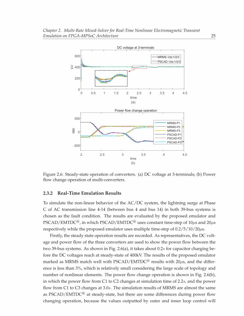
Chapter 2. Multi-Rate Mixed-Solver for Real-Time Nonlinear Electromagnetic TransientEmulation on FPGA-MPSoC Architecture 25
0 0.5 1 1.5 2 2.5 3 3.5 4 4.5time(a)
0
200
400
600
kV
DC voltage at 3-terminals
2 2.5 3 3.5 4 4.5time(b)
-500
0
500
MW
Power flow change operation
MRMS-P1MRMS-P2MRMS-P3PSCAD-P1PSCAD-P2PSCAD-P3
MRMS-Vdc1/2/3PSCAD-Vdc1/2/3
Figure 2.6: Steady-state operation of converters. (a) DC voltage at 3-terminals; (b) Powerflow change operation of multi-converters.
2.3.2 Real-Time Emulation Results
To simulate the non-linear behavior of the AC/DC system, the lightning surge at PhaseC of AC transmission line 4-14 (between bus 4 and bus 14) in both 39-bus systems ischosen as the fault condition. The results are evaluated by the proposed emulator andPSCAD/EMTDC�, in which PSCAD/EMTDC� uses constant time-step of 10μs and 20μsrespectively while the proposed emulator uses multiple time-step of 0.2/5/10/20μs.
Firstly, the steady state operation results are recorded. As representatives, the DC volt-age and power flow of the three converters are used to show the power flow between thetwo 39-bus systems. As shown in Fig. 2.6(a), it takes about 0.2s for capacitor charging be-fore the DC voltages reach at steady-state of 400kV. The results of the proposed emulatormarked as MRMS match well with PSCAD/EMTDC� results with 20μs, and the differ-ence is less than 3%, which is relatively small considering the large scale of topology andnumber of nonlinear elements. The power flow change operation is shown in Fig. 2.6(b),in which the power flow from C1 to C2 changes at simulation time of 2.2s, and the powerflow from C1 to C3 changes at 3.0s. The simulation results of MRMS are almost the sameas PSCAD/EMTDC� at steady-state, but there are some differences during power flowchanging operation, because the values outputted by outer and inner loop control will
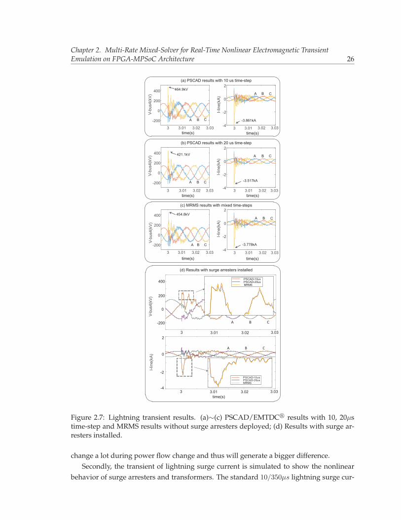
Chapter 2. Multi-Rate Mixed-Solver for Real-Time Nonlinear Electromagnetic TransientEmulation on FPGA-MPSoC Architecture 26
3 3.01 3.02 3.03-4
-2
0
2
I-line(kA)
3 3.01 3.02 3.03-4
-2
0
2
I-line(kA)
3 3.01 3.02 3.03
-200
0
200
400
V-bus4(kV)
3 3.01 3.02 3.03
-200
0
200
400V-bus4(kV)
3 3.01 3.02 3.03
-200
0
200
400
V-bus4(kV)
(a) PSCAD results with 10 us time-step
(b) PSCAD results with 20 us time-step
(c) MRMS results with mixed time-steps
A B C
A B C
A B C
A B C
A B C
A B C
464.9kV
421.1kV
454.8kV
-3.861kA
-3.517kA
-3.778kA
time(s) time(s)
time(s) time(s)
time(s) time(s)3 3.01 3.02 3.03
-4
-2
0
2
I-line(kA)
(d) Results with surge arresters installed
time(s)
V-bus4(kV)
I-line(kA)
0
200
400
-200
0
-2
-4
2
A B C
PSCAD-10usPSCAD-20usMRMS
3 3.01 3.02 3.03
A B C
PSCAD-10usPSCAD-20usMRMS
3 3.01 3.02 3.03
Figure 2.7: Lightning transient results. (a)∼(c) PSCAD/EMTDC� results with 10, 20μstime-step and MRMS results without surge arresters deployed; (d) Results with surge ar-resters installed.
change a lot during power flow change and thus will generate a bigger difference.Secondly, the transient of lightning surge current is simulated to show the nonlinear
behavior of surge arresters and transformers. The standard 10/350μs lightning surge cur-
Chapter 2. Multi-Rate Mixed-Solver for Real-Time Nonlinear Electromagnetic TransientEmulation on FPGA-MPSoC Architecture 27
rent [59] is applied in this work, given as:
ILS(t) = CIm(t/τ1)ke−tτ2 /[1 + (t/τ1)
k] (2.18)
where the coefficient C = 1.075, k = 10; the time constant τ1 = 19μs, τ2 = 485μs; themaximum value of the surge current Im = 10kA. In this simulation, the lightning surgecurrent is applied at exactly 3s of the simulation, and the results without and with surgearresters are shown in Fig. 2.7(a)∼(c) and (d) respectively. The peak value and transientdetails of surge voltage and current without surge arresters installed indicate that changingthe time-step value will significantly impact the accuracy. MRMS uses mixed time-step of0.2/5/10/20μs, and the results are more reasonable than the PSCAD/EMTDC� resultswith 20μs time-step and are close to that of 10μs. When the surge arresters are installed,MRMS uses the iterative solver to solve the nonlinear elements for accuracy, although thenonlinear function is simplified to piecewise linear segments. But in PSCAD/EMTDC�,the piecewise linear method is used to deal with the nonlinearity of surge arresters. Asshown in Fig. 2.7(d), the MRMS results are close to those of the PSCAD/EMTDC� with10μs time-step, and can even show more details although there is not a judgement whichone is more correct.
2.4 Summary
To optimize the accuracy as well as the resource cost, a novel multi-rate mixed-solver hard-ware emulation architecture is proposed. In the proposed solver, the power system isdecomposed into several subsystems, in which multiple time-steps are applied for differ-ent subsystems according to the accuracy requirements; by applying the iterative schemeslocally and reusing the linear solver among subsystems, the computational resource con-sumption is reduced. The AC/DC network composed of two IEEE 39-bus systems andthree MMC converters is emulated in real-time on the hybrid FPGA-MPSoC platform. Theprocessing delay of different subsystems and solvers is evaluated, which shows the prac-ticality of multi-rate with 0.2/5/10/20μs time-steps applied. The multi-rate mixed-solvercan be used for large AC/DC system simulations that consist of various types of elementswith requirements of high accuracy and optimum computation resource consumption. Inthe future work, the emulation system can be further enlarged with more complicatednonlinear models [60–63] for conventional power equipment as well as power electronicapparatus.
3Variable Time-Stepping Universal Line and
Machine Models and Implementation onFPGA and GPU Platforms
In the conventional EMT simulator the time-step is fixed, which may lead to inefficiencieswhen the time constants of the system change. The variable time-stepping (VTS) methodcan efficaciously solve this problem; however, the VTS schemes for the universal trans-mission line model (ULM) and universal machine (UM) model remain to be investigated.This chapter derives the VTS models for ULM and UM, and the proposed ULM model ismore stable than the traditional model. Both VTS models combined with other equipmentare emulated on the parallel architecture of the FPGA and GPU platform. The proposedhierarchical VTS scheme and the local truncation error (LTE) based time-step control en-able the large-scale systems to be simulated in real-time and “faster-than-real-time” modeson FPGA. The 4-level massively parallel VTS simulation architecture is also proposed forGPU implementation. The IEEE 39-bus and 118-bus test power systems with VTS modelswere emulated on FPGA and GPU boards respectively, and the emulation results com-pared with PSCAD/EMTDC� and fixed time-stepping (FTS) hardware emulator verifiedthe effectiveness of the proposed models and implementation architectures.
3.1 Universal Transmission Line Model Computation
The ULM and UM model computation for VTS is not the same as that for the fixed time-step because the model parameters may change when the time-step changes. The equiva-lent circuit for ULM is shown in Fig. 3.1, in which the two ends (k and m) of the line areabstracted into two disconnected parts, and each part combines an equivalent conductance
28
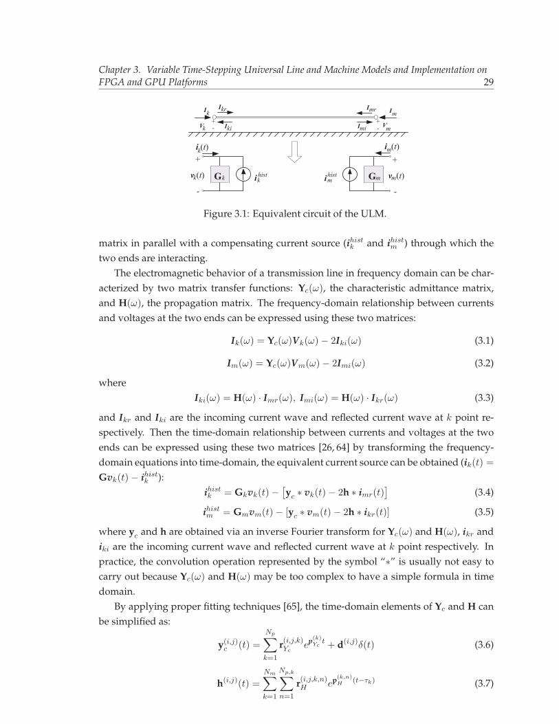
Chapter 3. Variable Time-Stepping Universal Line and Machine Models and Implementation onFPGA and GPU Platforms 29
+
-
I
Gv (t)k
i (t)k
ikhist+
-
Gimhist v (t)m
i (t)m
k +
-Vk
Im
- mV
+
Ikr
Iki
Imr
Imi
k m
Figure 3.1: Equivalent circuit of the ULM.
matrix in parallel with a compensating current source (ihistk and ihistm ) through which thetwo ends are interacting.
The electromagnetic behavior of a transmission line in frequency domain can be char-acterized by two matrix transfer functions: Yc(ω), the characteristic admittance matrix,and H(ω), the propagation matrix. The frequency-domain relationship between currentsand voltages at the two ends can be expressed using these two matrices:
Ik(ω) = Yc(ω)Vk(ω)− 2Iki(ω) (3.1)
Im(ω) = Yc(ω)Vm(ω)− 2Imi(ω) (3.2)
whereIki(ω) = H(ω) · Imr(ω), Imi(ω) = H(ω) · Ikr(ω) (3.3)
and Ikr and Iki are the incoming current wave and reflected current wave at k point re-spectively. Then the time-domain relationship between currents and voltages at the twoends can be expressed using these two matrices [26, 64] by transforming the frequency-domain equations into time-domain, the equivalent current source can be obtained (ik(t) =Gvk(t)− ihistk ):
ihistk = Gkvk(t)−[yc ∗ vk(t)− 2h ∗ imr(t)
](3.4)
ihistm = Gmvm(t)− [yc ∗ vm(t)− 2h ∗ ikr(t)] (3.5)
where yc and h are obtained via an inverse Fourier transform for Yc(ω) and H(ω), ikr andiki are the incoming current wave and reflected current wave at k point respectively. Inpractice, the convolution operation represented by the symbol “∗” is usually not easy tocarry out because Yc(ω) and H(ω) may be too complex to have a simple formula in timedomain.
By applying proper fitting techniques [65], the time-domain elements of Yc and H canbe simplified as:
y(i,j)c (t) =
Np∑k=1
r(i,j,k)Ycep(k)
Yct + d(i,j)δ(t) (3.6)
h(i,j)(t) =
Nm∑k=1
Np,k∑n=1
r(i,j,k,n)H ep(k,n)H (t−τk) (3.7)
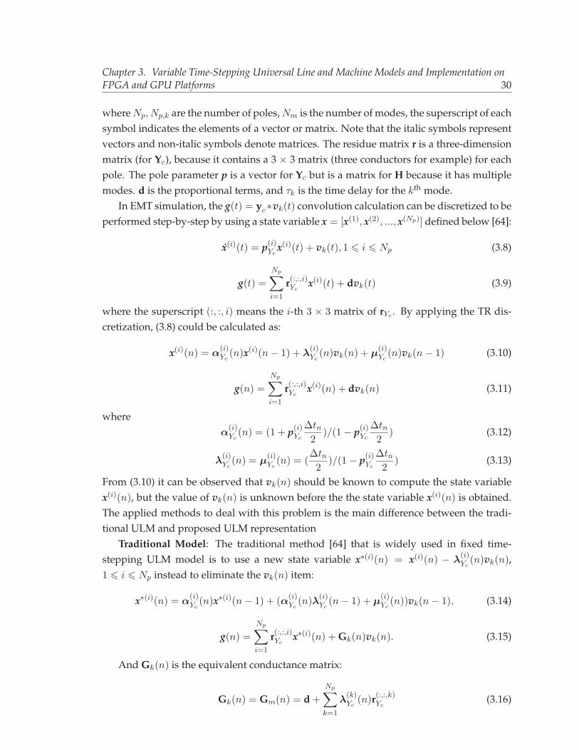
Chapter 3. Variable Time-Stepping Universal Line and Machine Models and Implementation onFPGA and GPU Platforms 30
where Np, Np,k are the number of poles, Nm is the number of modes, the superscript of eachsymbol indicates the elements of a vector or matrix. Note that the italic symbols representvectors and non-italic symbols denote matrices. The residue matrix r is a three-dimensionmatrix (for Yc), because it contains a 3 × 3 matrix (three conductors for example) for eachpole. The pole parameter p is a vector for Yc but is a matrix for H because it has multiplemodes. d is the proportional terms, and τk is the time delay for the kth mode.
In EMT simulation, the g(t) = yc∗vk(t) convolution calculation can be discretized to beperformed step-by-step by using a state variable x = [x(1), x(2), ..., x(Np)] defined below [64]:
x(i)(t) = p(i)Yc
x(i)(t) + vk(t), 1 � i � Np (3.8)
g(t) =Np∑i=1
r(:,:,i)Ycx(i)(t) + dvk(t) (3.9)
where the superscript (:, :, i) means the i-th 3 × 3 matrix of rYc . By applying the TR dis-cretization, (3.8) could be calculated as:
x(i)(n) = α(i)Yc(n)x(i)(n− 1) + λ
(i)Yc(n)vk(n) + μ
(i)Yc(n)vk(n− 1) (3.10)
g(n) =Np∑i=1
r(:,:,i)Ycx(i)(n) + dvk(n) (3.11)
whereα
(i)Yc(n) = (1 + p(i)
Yc
Δtn2
)/(1− p(i)Yc
Δtn2
) (3.12)
λ(i)Yc(n) = μ
(i)Yc(n) = (
Δtn2
)/(1− p(i)Yc
Δtn2
) (3.13)
From (3.10) it can be observed that vk(n) should be known to compute the state variablex(i)(n), but the value of vk(n) is unknown before the the state variable x(i)(n) is obtained.The applied methods to deal with this problem is the main difference between the tradi-tional ULM and proposed ULM representation
Traditional Model: The traditional method [64] that is widely used in fixed time-stepping ULM model is to use a new state variable x∗(i)(n) = x(i)(n) − λ
(i)Yc(n)vk(n),
1 � i � Np instead to eliminate the vk(n) item:
x∗(i)(n) = α(i)Yc(n)x∗(i)(n− 1) + (α
(i)Yc(n)λ
(i)Yc(n− 1) + μ
(i)Yc(n))vk(n− 1), (3.14)
g(n) =Np∑i=1
r(:,:,i)Ycx∗(i)(n) + Gk(n)vk(n). (3.15)
And Gk(n) is the equivalent conductance matrix:
Gk(n) = Gm(n) = d +
Np∑k=1
λ(k)Yc
(n)r(:,:,k)Yc(3.16)
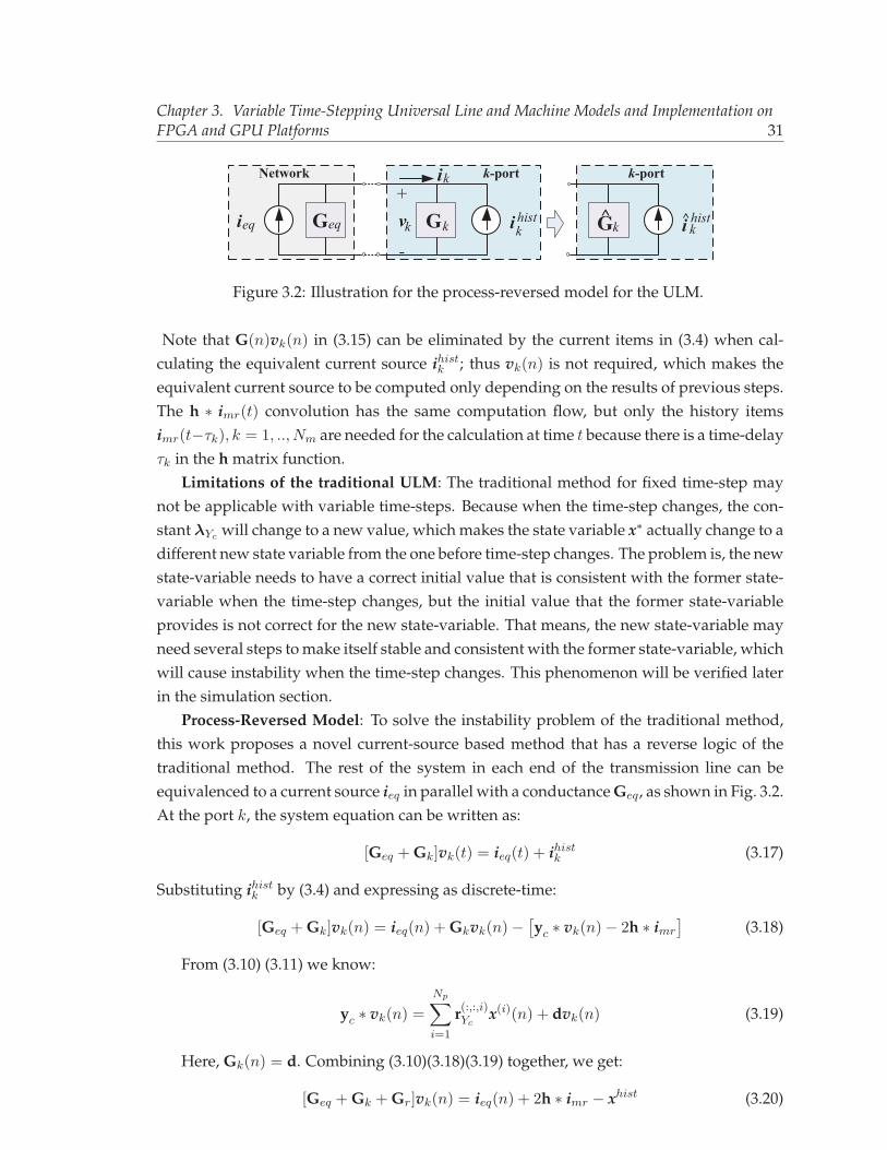
Chapter 3. Variable Time-Stepping Universal Line and Machine Models and Implementation onFPGA and GPU Platforms 31
+
-Gvk
ik
ikhistGieq keq
Network k-port
G i khistk
k-port
^ ^
Figure 3.2: Illustration for the process-reversed model for the ULM.
Note that G(n)vk(n) in (3.15) can be eliminated by the current items in (3.4) when cal-culating the equivalent current source ihistk ; thus vk(n) is not required, which makes theequivalent current source to be computed only depending on the results of previous steps.The h ∗ imr(t) convolution has the same computation flow, but only the history itemsimr(t−τk), k = 1, .., Nm are needed for the calculation at time t because there is a time-delayτk in the h matrix function.
Limitations of the traditional ULM: The traditional method for fixed time-step maynot be applicable with variable time-steps. Because when the time-step changes, the con-stant λYc will change to a new value, which makes the state variable x∗ actually change to adifferent new state variable from the one before time-step changes. The problem is, the newstate-variable needs to have a correct initial value that is consistent with the former state-variable when the time-step changes, but the initial value that the former state-variableprovides is not correct for the new state-variable. That means, the new state-variable mayneed several steps to make itself stable and consistent with the former state-variable, whichwill cause instability when the time-step changes. This phenomenon will be verified laterin the simulation section.
Process-Reversed Model: To solve the instability problem of the traditional method,this work proposes a novel current-source based method that has a reverse logic of thetraditional method. The rest of the system in each end of the transmission line can beequivalenced to a current source ieq in parallel with a conductance Geq, as shown in Fig. 3.2.At the port k, the system equation can be written as:
[Geq + Gk]vk(t) = ieq(t) + ihistk (3.17)
Substituting ihistk by (3.4) and expressing as discrete-time:
[Geq + Gk]vk(n) = ieq(n) + Gkvk(n)−[yc ∗ vk(n)− 2h ∗ imr
](3.18)
From (3.10) (3.11) we know:
yc ∗ vk(n) =
Np∑i=1
r(:,:,i)Ycx(i)(n) + dvk(n) (3.19)
Here, Gk(n) = d. Combining (3.10)(3.18)(3.19) together, we get:
[Geq + Gk + Gr]vk(n) = ieq(n) + 2h ∗ imr − xhist (3.20)
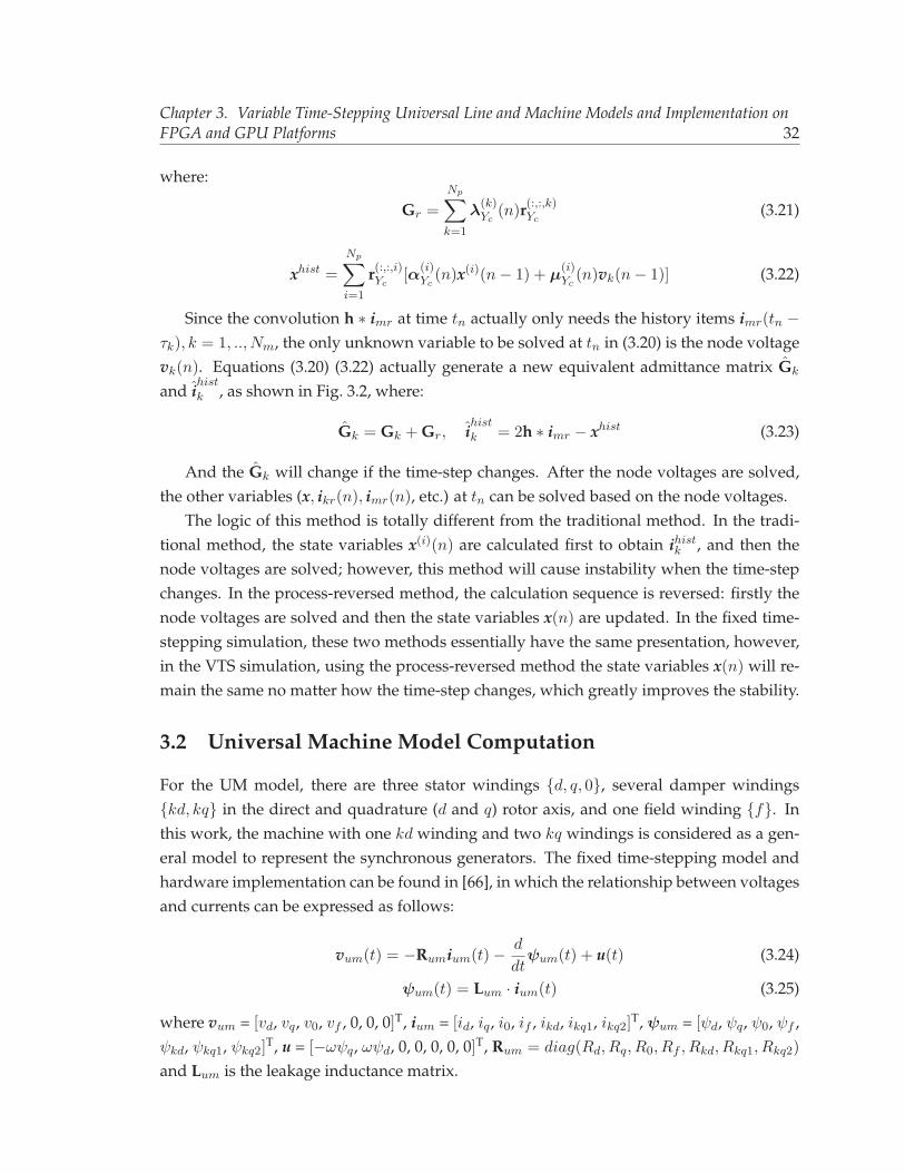
Chapter 3. Variable Time-Stepping Universal Line and Machine Models and Implementation onFPGA and GPU Platforms 32
where:
Gr =
Np∑k=1
λ(k)Yc
(n)r(:,:,k)Yc(3.21)
xhist =Np∑i=1
r(:,:,i)Yc[α
(i)Yc(n)x(i)(n− 1) + μ
(i)Yc(n)vk(n− 1)] (3.22)
Since the convolution h ∗ imr at time tn actually only needs the history items imr(tn −τk), k = 1, .., Nm, the only unknown variable to be solved at tn in (3.20) is the node voltagevk(n). Equations (3.20) (3.22) actually generate a new equivalent admittance matrix Gk
and ihist
k , as shown in Fig. 3.2, where:
Gk = Gk + Gr, ihist
k = 2h ∗ imr − xhist (3.23)
And the Gk will change if the time-step changes. After the node voltages are solved,the other variables (x, ikr(n), imr(n), etc.) at tn can be solved based on the node voltages.
The logic of this method is totally different from the traditional method. In the tradi-tional method, the state variables x(i)(n) are calculated first to obtain ihistk , and then thenode voltages are solved; however, this method will cause instability when the time-stepchanges. In the process-reversed method, the calculation sequence is reversed: firstly thenode voltages are solved and then the state variables x(n) are updated. In the fixed time-stepping simulation, these two methods essentially have the same presentation, however,in the VTS simulation, using the process-reversed method the state variables x(n) will re-main the same no matter how the time-step changes, which greatly improves the stability.
3.2 Universal Machine Model Computation
For the UM model, there are three stator windings {d, q, 0}, several damper windings{kd, kq} in the direct and quadrature (d and q) rotor axis, and one field winding {f}. Inthis work, the machine with one kd winding and two kq windings is considered as a gen-eral model to represent the synchronous generators. The fixed time-stepping model andhardware implementation can be found in [66], in which the relationship between voltagesand currents can be expressed as follows:
vum(t) = −Rumium(t)− d
dtψum(t) + u(t) (3.24)
ψum(t) = Lum · ium(t) (3.25)
where vum = [vd, vq, v0, vf , 0, 0, 0]T, ium = [id, iq, i0, if , ikd, ikq1, ikq2]T, ψum = [ψd, ψq, ψ0, ψf ,ψkd, ψkq1, ψkq2]
T, u = [−ωψq, ωψd, 0, 0, 0, 0, 0]T, Rum = diag(Rd, Rq, R0, Rf , Rkd, Rkq1, Rkq2)
and Lum is the leakage inductance matrix.
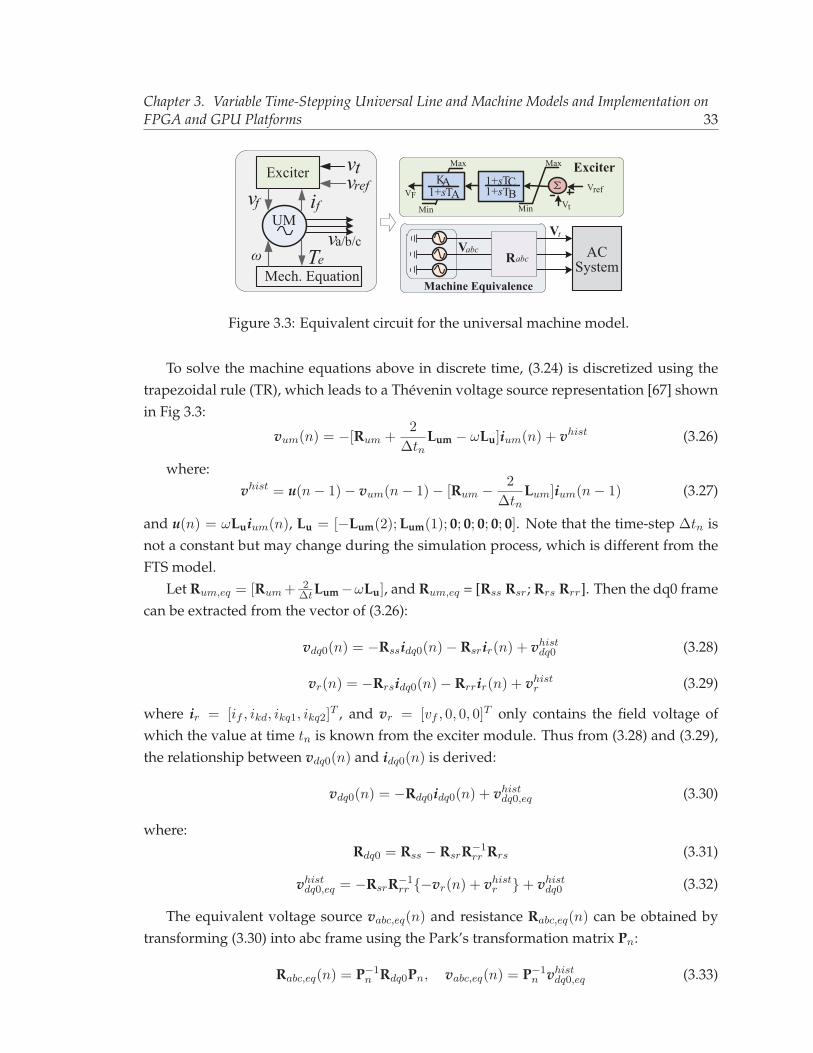
Chapter 3. Variable Time-Stepping Universal Line and Machine Models and Implementation onFPGA and GPU Platforms 33
ACSystem
UM
ExciterExciter
ifvfvref
Mech. EquationTeω
tv
a/b/cvRabc
Vref
Vt
TC1+sTB1+s
KATA1+s
Max
Min
VF
Max
Min
VabcVt
Machine Equivalence
Figure 3.3: Equivalent circuit for the universal machine model.
To solve the machine equations above in discrete time, (3.24) is discretized using thetrapezoidal rule (TR), which leads to a Thevenin voltage source representation [67] shownin Fig 3.3:
vum(n) = −[Rum +2
ΔtnLum − ωLu]ium(n) + vhist (3.26)
where:vhist = u(n− 1)− vum(n− 1)− [Rum − 2
ΔtnLum]ium(n− 1) (3.27)
and u(n) = ωLuium(n), Lu = [−Lum(2);Lum(1); 0; 0; 0; 0; 0]. Note that the time-step Δtn isnot a constant but may change during the simulation process, which is different from theFTS model.
Let Rum,eq = [Rum+ 2ΔtLum −ωLu], and Rum,eq = [Rss Rsr; Rrs Rrr]. Then the dq0 frame
can be extracted from the vector of (3.26):
vdq0(n) = −Rssidq0(n)− Rsrir(n) + vhistdq0 (3.28)
vr(n) = −Rrsidq0(n)− Rrrir(n) + vhistr (3.29)
where ir = [if , ikd, ikq1, ikq2]T , and vr = [vf , 0, 0, 0]
T only contains the field voltage ofwhich the value at time tn is known from the exciter module. Thus from (3.28) and (3.29),the relationship between vdq0(n) and idq0(n) is derived:
vdq0(n) = −Rdq0idq0(n) + vhistdq0,eq (3.30)
where:Rdq0 = Rss − RsrR−1rr Rrs (3.31)
vhistdq0,eq = −RsrR−1rr {−vr(n) + vhist
r }+ vhistdq0 (3.32)
The equivalent voltage source vabc,eq(n) and resistance Rabc,eq(n) can be obtained bytransforming (3.30) into abc frame using the Park’s transformation matrix Pn:
Rabc,eq(n) = P−1n Rdq0Pn, vabc,eq(n) = P−1n vhistdq0,eq (3.33)
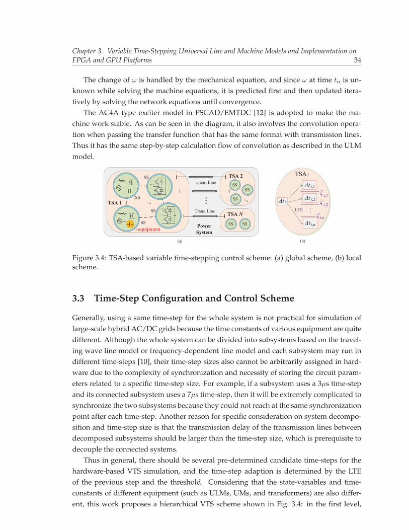
Chapter 3. Variable Time-Stepping Universal Line and Machine Models and Implementation onFPGA and GPU Platforms 34
The change of ω is handled by the mechanical equation, and since ω at time tn is un-known while solving the machine equations, it is predicted first and then updated itera-tively by solving the network equations until convergence.
The AC4A type exciter model in PSCAD/EMTDC [12] is adopted to make the ma-chine work stable. As can be seen in the diagram, it also involves the convolution opera-tion when passing the transfer function that has the same format with transmission lines.Thus it has the same step-by-step calculation flow of convolution as described in the ULMmodel.
TSA 1SS
SS
SS
SS
...
Trans. Line
equipment
...
...
...
...
TSA 2
...
TSA NTrans. Line
PowerSystem
...
TSA i
Δt
Δt i,1
i
Δti,n
Δt i,2ξ i,1ξ
ξ
…
LTEi,2
i,n
(a) (b)
SSSS
SS
SS SS
Figure 3.4: TSA-based variable time-stepping control scheme: (a) global scheme, (b) localscheme.
3.3 Time-Step Configuration and Control Scheme
Generally, using a same time-step for the whole system is not practical for simulation oflarge-scale hybrid AC/DC grids because the time constants of various equipment are quitedifferent. Although the whole system can be divided into subsystems based on the travel-ing wave line model or frequency-dependent line model and each subsystem may run indifferent time-steps [10], their time-step sizes also cannot be arbitrarily assigned in hard-ware due to the complexity of synchronization and necessity of storing the circuit param-eters related to a specific time-step size. For example, if a subsystem uses a 3μs time-stepand its connected subsystem uses a 7μs time-step, then it will be extremely complicated tosynchronize the two subsystems because they could not reach at the same synchronizationpoint after each time-step. Another reason for specific consideration on system decompo-sition and time-step size is that the transmission delay of the transmission lines betweendecomposed subsystems should be larger than the time-step size, which is prerequisite todecouple the connected systems.
Thus in general, there should be several pre-determined candidate time-steps for thehardware-based VTS simulation, and the time-step adaption is determined by the LTEof the previous step and the threshold. Considering that the state-variables and time-constants of different equipment (such as ULMs, UMs, and transformers) are also differ-ent, this work proposes a hierarchical VTS scheme shown in Fig. 3.4: in the first level,
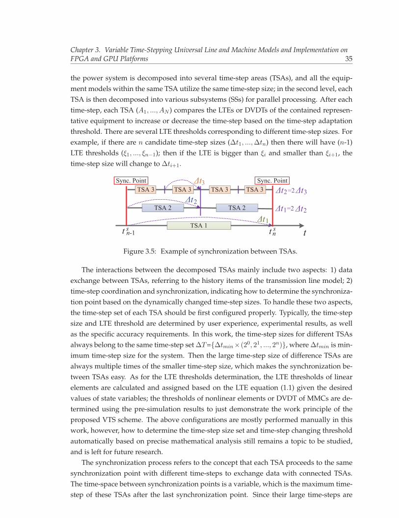
Chapter 3. Variable Time-Stepping Universal Line and Machine Models and Implementation onFPGA and GPU Platforms 35
the power system is decomposed into several time-step areas (TSAs), and all the equip-ment models within the same TSA utilize the same time-step size; in the second level, eachTSA is then decomposed into various subsystems (SSs) for parallel processing. After eachtime-step, each TSA (A1, ..., AN ) compares the LTEs or DVDTs of the contained represen-tative equipment to increase or decrease the time-step based on the time-step adaptationthreshold. There are several LTE thresholds corresponding to different time-step sizes. Forexample, if there are n candidate time-step sizes (Δt1, ...,Δtn) then there will have (n-1)LTE thresholds (ξ1, ..., ξn−1); then if the LTE is bigger than ξi and smaller than ξi+1, thetime-step size will change to Δti+1.
Δt1TSA 1
TSA 2 TSA 2
t sn-1 t sn t
Δt2TSA 3 TSA 3 TSA 3 TSA 3
Δt3
Δt1=2 Δt2
Δt2 Δt3=2Sync. PointSync. Point
Figure 3.5: Example of synchronization between TSAs.
The interactions between the decomposed TSAs mainly include two aspects: 1) dataexchange between TSAs, referring to the history items of the transmission line model; 2)time-step coordination and synchronization, indicating how to determine the synchroniza-tion point based on the dynamically changed time-step sizes. To handle these two aspects,the time-step set of each TSA should be first configured properly. Typically, the time-stepsize and LTE threshold are determined by user experience, experimental results, as wellas the specific accuracy requirements. In this work, the time-step sizes for different TSAsalways belong to the same time-step set ΔT={Δtmin× (20, 21, ..., 2n)}, where Δtmin is min-imum time-step size for the system. Then the large time-step size of difference TSAs arealways multiple times of the smaller time-step size, which makes the synchronization be-tween TSAs easy. As for the LTE thresholds determination, the LTE thresholds of linearelements are calculated and assigned based on the LTE equation (1.1) given the desiredvalues of state variables; the thresholds of nonlinear elements or DVDT of MMCs are de-termined using the pre-simulation results to just demonstrate the work principle of theproposed VTS scheme. The above configurations are mostly performed manually in thiswork, however, how to determine the time-step size set and time-step changing thresholdautomatically based on precise mathematical analysis still remains a topic to be studied,and is left for future research.
The synchronization process refers to the concept that each TSA proceeds to the samesynchronization point with different time-steps to exchange data with connected TSAs.The time-space between synchronization points is a variable, which is the maximum time-step of these TSAs after the last synchronization point. Since their large time-steps are
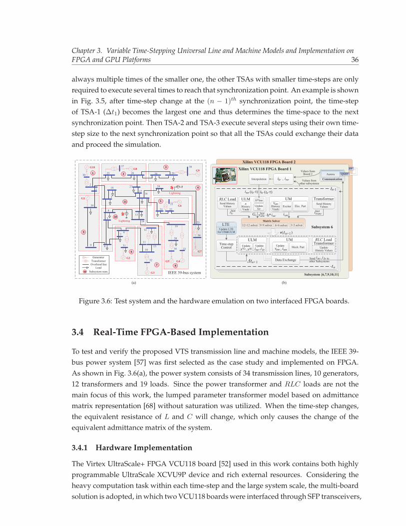
Chapter 3. Variable Time-Stepping Universal Line and Machine Models and Implementation onFPGA and GPU Platforms 36
always multiple times of the smaller one, the other TSAs with smaller time-steps are onlyrequired to execute several times to reach that synchronization point. An example is shownin Fig. 3.5, after time-step change at the (n − 1)th synchronization point, the time-stepof TSA-1 (Δt1) becomes the largest one and thus determines the time-space to the nextsynchronization point. Then TSA-2 and TSA-3 execute several steps using their own time-step size to the next synchronization point so that all the TSAs could exchange their dataand proceed the simulation.
QSFP37
25
2
1
30
39
9 8
76
5
4
3110
11
12
13
15
163
1817
26
27
28 29
24
19
20
32
34 33
21 22
35
23
36
38
14
Lightning
IEEE 39-bus system
Overhead line
Generator
Load
Transformer
G10 G8 G9
G1
G2
G3
G7
G5 G4
G6
Xilinx VCU118 FPGA Board 1
Matrix Solver
Communication
Aurora
9×9 solver 6×6 solver 3×3 solver12×12 solver
QSFPValues fromBoard 2
kri mri,Interpolation
n-1t
nt
kri (t - )τ nmri (t - )τ n
H*Imr
Update LTEfor UM&ULM
Send HistoryValues
RLC Load ULMSend History
Values
Transformer
UpdateHistory Values
Transformer
xHistoryVaule
UpdateGr
Elec. Part
UM
HistoryVaule
lcihistulmxhistrG transihist
umimri,h*
umvExciter
Subsystem 6v( )n+1t
Update
ULMUpdate
UMUpdate Mech. PartumvxYc xH mri, , kri
Time-stepControl
Send toother Subsystems
mri kri,Data Exchange
(a) (b)
9
11
1
xx Subsystem num.
2
3
5
4
6
7 8
10
RLC Load
LTE
Δtn+1
Lightning
Xilinx VCU118 FPGA Board 2
umi,
Subsystem {6,7,9,10,11}
Values fromother subsystems
Figure 3.6: Test system and the hardware emulation on two interfaced FPGA boards.
3.4 Real-Time FPGA-Based Implementation
To test and verify the proposed VTS transmission line and machine models, the IEEE 39-bus power system [57] was first selected as the case study and implemented on FPGA.As shown in Fig. 3.6(a), the power system consists of 34 transmission lines, 10 generators,12 transformers and 19 loads. Since the power transformer and RLC loads are not themain focus of this work, the lumped parameter transformer model based on admittancematrix representation [68] without saturation was utilized. When the time-step changes,the equivalent resistance of L and C will change, which only causes the change of theequivalent admittance matrix of the system.
3.4.1 Hardware Implementation
The Virtex UltraScale+ FPGA VCU118 board [52] used in this work contains both highlyprogrammable UltraScale XCVU9P device and rich external resources. Considering theheavy computation task within each time-step and the large system scale, the multi-boardsolution is adopted, in which two VCU118 boards were interfaced through SFP transceivers,
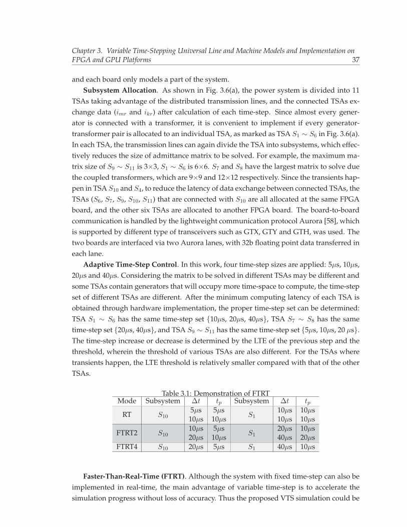
Chapter 3. Variable Time-Stepping Universal Line and Machine Models and Implementation onFPGA and GPU Platforms 37
and each board only models a part of the system.Subsystem Allocation. As shown in Fig. 3.6(a), the power system is divided into 11
TSAs taking advantage of the distributed transmission lines, and the connected TSAs ex-change data (imr and ikr) after calculation of each time-step. Since almost every gener-ator is connected with a transformer, it is convenient to implement if every generator-transformer pair is allocated to an individual TSA, as marked as TSA S1 ∼ S6 in Fig. 3.6(a).In each TSA, the transmission lines can again divide the TSA into subsystems, which effec-tively reduces the size of admittance matrix to be solved. For example, the maximum ma-trix size of S9 ∼ S11 is 3×3, S1 ∼ S6 is 6×6. S7 and S8 have the largest matrix to solve duethe coupled transformers, which are 9×9 and 12×12 respectively. Since the transients hap-pen in TSA S10 and S4, to reduce the latency of data exchange between connected TSAs, theTSAs (S6, S7, S9, S10, S11) that are connected with S10 are all allocated at the same FPGAboard, and the other six TSAs are allocated to another FPGA board. The board-to-boardcommunication is handled by the lightweight communication protocol Aurora [58], whichis supported by different type of transceivers such as GTX, GTY and GTH, was used. Thetwo boards are interfaced via two Aurora lanes, with 32b floating point data transferred ineach lane.
Adaptive Time-Step Control. In this work, four time-step sizes are applied: 5μs, 10μs,20μs and 40μs. Considering the matrix to be solved in different TSAs may be different andsome TSAs contain generators that will occupy more time-space to compute, the time-stepset of different TSAs are different. After the minimum computing latency of each TSA isobtained through hardware implementation, the proper time-step set can be determined:TSA S1 ∼ S6 has the same time-step set {10μs, 20μs, 40μs}, TSA S7 ∼ S8 has the sametime-step set {20μs, 40μs}, and TSA S9 ∼ S11 has the same time-step set {5μs, 10μs, 20 μs}.The time-step increase or decrease is determined by the LTE of the previous step and thethreshold, wherein the threshold of various TSAs are also different. For the TSAs wheretransients happen, the LTE threshold is relatively smaller compared with that of the otherTSAs.
Table 3.1: Demonstration of FTRTMode Subsystem Δt tp Subsystem Δt tp
5μs 5μs 10μs 10μsRT S10 10μs 10μs
S1 10μs 10μs10μs 5μs 20μs 10μs
FTRT2 S10 20μs 10μsS1 40μs 20μs
FTRT4 S10 20μs 5μs S1 40μs 10μs
Faster-Than-Real-Time (FTRT). Although the system with fixed time-step can also beimplemented in real-time, the main advantage of variable time-step is to accelerate thesimulation progress without loss of accuracy. Thus the proposed VTS simulation could be
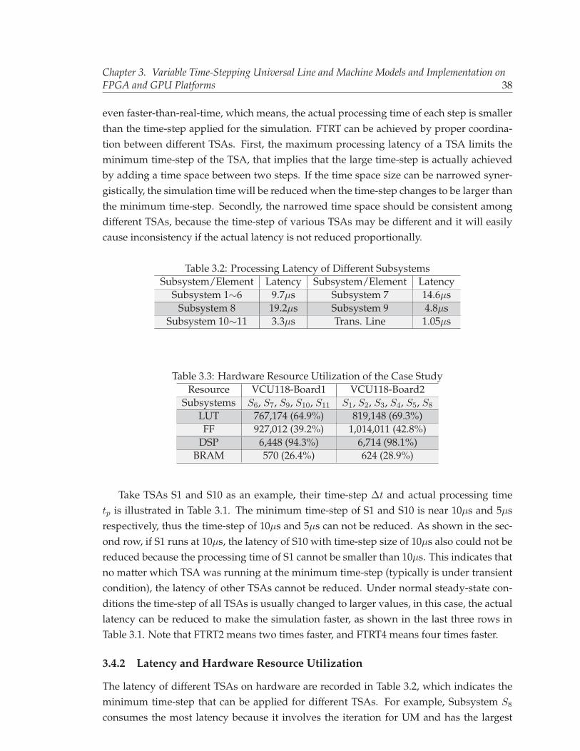
Chapter 3. Variable Time-Stepping Universal Line and Machine Models and Implementation onFPGA and GPU Platforms 38
even faster-than-real-time, which means, the actual processing time of each step is smallerthan the time-step applied for the simulation. FTRT can be achieved by proper coordina-tion between different TSAs. First, the maximum processing latency of a TSA limits theminimum time-step of the TSA, that implies that the large time-step is actually achievedby adding a time space between two steps. If the time space size can be narrowed syner-gistically, the simulation time will be reduced when the time-step changes to be larger thanthe minimum time-step. Secondly, the narrowed time space should be consistent amongdifferent TSAs, because the time-step of various TSAs may be different and it will easilycause inconsistency if the actual latency is not reduced proportionally.
Table 3.2: Processing Latency of Different SubsystemsSubsystem/Element Latency Subsystem/Element Latency
Subsystem 1∼6 9.7μs Subsystem 7 14.6μsSubsystem 8 19.2μs Subsystem 9 4.8μs
Subsystem 10∼11 3.3μs Trans. Line 1.05μs
Table 3.3: Hardware Resource Utilization of the Case StudyResource VCU118-Board1 VCU118-Board2
Subsystems S6, S7, S9, S10, S11 S1, S2, S3, S4, S5, S8
LUT 767,174 (64.9%) 819,148 (69.3%)FF 927,012 (39.2%) 1,014,011 (42.8%)
DSP 6,448 (94.3%) 6,714 (98.1%)BRAM 570 (26.4%) 624 (28.9%)
Take TSAs S1 and S10 as an example, their time-step Δt and actual processing timetp is illustrated in Table 3.1. The minimum time-step of S1 and S10 is near 10μs and 5μsrespectively, thus the time-step of 10μs and 5μs can not be reduced. As shown in the sec-ond row, if S1 runs at 10μs, the latency of S10 with time-step size of 10μs also could not bereduced because the processing time of S1 cannot be smaller than 10μs. This indicates thatno matter which TSA was running at the minimum time-step (typically is under transientcondition), the latency of other TSAs cannot be reduced. Under normal steady-state con-ditions the time-step of all TSAs is usually changed to larger values, in this case, the actuallatency can be reduced to make the simulation faster, as shown in the last three rows inTable 3.1. Note that FTRT2 means two times faster, and FTRT4 means four times faster.
3.4.2 Latency and Hardware Resource Utilization
The latency of different TSAs on hardware are recorded in Table 3.2, which indicates theminimum time-step that can be applied for different TSAs. For example, Subsystem S8
consumes the most latency because it involves the iteration for UM and has the largest
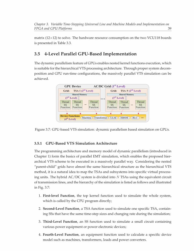
Chapter 3. Variable Time-Stepping Universal Line and Machine Models and Implementation onFPGA and GPU Platforms 39
matrix (12×12) to solve. The hardware resource consumption on the two VCU118 boardsis presented in Table 3.3.
3.5 4-Level Parallel GPU-Based Implementation
The dynamic parallelism feature of GPUs enables nested kernel functions execution, whichis suitable for the hierarchical VTS processing architecture. Through proper system decom-position and GPU run-time configurations, the massively parallel VTS simulation can beachieved.
GPU Device AC/DC Grid (1st Level)TSA 1 (2nd Level)
Shared Memory
Device Functions(4th Level) Machine Transformer ULM ...HBSM
Grid:
......
ThreadSS
Function
RLC
TSA N (2nd Level)Shared Memory
Grid:
(3rd Level) (3rd Level)ThreadSS
Function
ThreadSS
Function
ThreadSS
Function
ThreadSS
Function
ThreadSS
Function...
Figure 3.7: GPU-based VTS simulation: dynamic parallelism based simulation on GPUs.
3.5.1 GPU-Based VTS Simulation Architecture
The programming architecture and memory model of dynamic parallelism (introduced inChapter 1) form the basics of parallel EMT simulation, which enables the proposed hier-archical VTS scheme to be executed in a massively parallel way. Considering the nested“parent-child” grids have almost the same hierarchical structure as the hierarchical VTSmethod, it is a natural idea to map the TSAs and subsystems into specific virtual process-ing units. The hybrid AC/DC system is divided into N TSAs using the equivalent circuitof transmission lines, and the hierarchy of the simulation is listed as follows and illustratedin Fig. 3.7:
1. First-level Function, the top kernel function used to simulate the whole system,which is called by the CPU program directly;
2. Second-Level Function, a TSA function used to simulate one specific TSA, contain-ing SSs that have the same time-step sizes and changing rate during the simulation;
3. Third-Level Function, an SS function used to simulate a small circuit containingvarious power equipment or power electronic devices;
4. Fourth-Level Function, an equipment function used to calculate a specific devicemodel such as machines, transformers, loads and power converters.
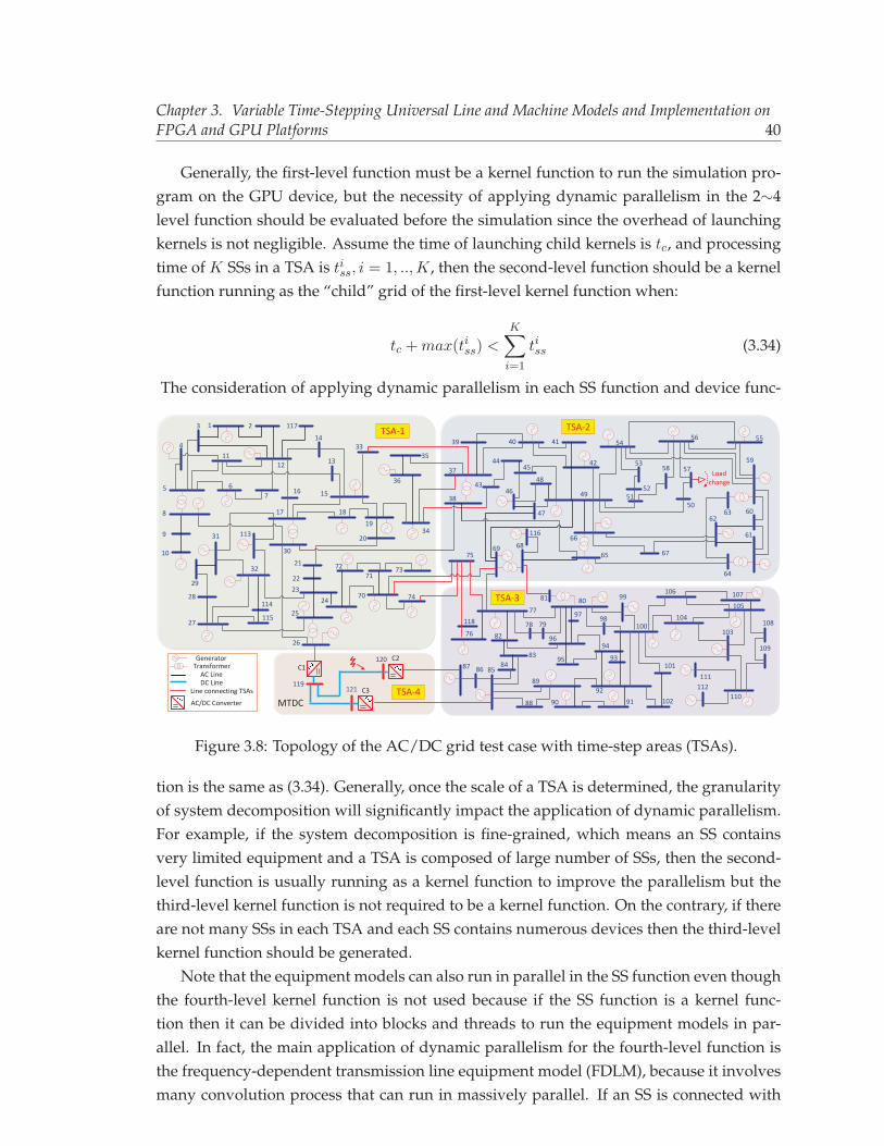
Chapter 3. Variable Time-Stepping Universal Line and Machine Models and Implementation onFPGA and GPU Platforms 40
Generally, the first-level function must be a kernel function to run the simulation pro-gram on the GPU device, but the necessity of applying dynamic parallelism in the 2∼4level function should be evaluated before the simulation since the overhead of launchingkernels is not negligible. Assume the time of launching child kernels is tc, and processingtime of K SSs in a TSA is tiss, i = 1, ..,K, then the second-level function should be a kernelfunction running as the “child” grid of the first-level kernel function when:
tc +max(tiss) <
K∑i=1
tiss (3.34)
The consideration of applying dynamic parallelism in each SS function and device func-
3 1
AC Line
GeneratorTransformer
2 117
12
1433
35
36
13
1576
4
5
11
8
9
16
17 18
19
10
2034
30
31 113
21
2229
28
27
2324
25
26
115
114
32 7271
70 74
73
75
37
43
38
69
39 40 41
4445 42
4648
49
47
5150
52
53
54
58 57
56 55
59
60
61
63
66
65 67
62
64
116
68
81
7780 99
106 107
104105
1009897
9694
95 93
9289
90 91
87 86 85
118
76 82
8384
88
101
102 110
108
109
103
111112
78 79
Line connecting TSAs
MTDC
119
120C1
C2
C3121DC Line
AC/DC Converter
Loadchange
TSA-1 TSA-2
TSA-3
TSA-4
Figure 3.8: Topology of the AC/DC grid test case with time-step areas (TSAs).
tion is the same as (3.34). Generally, once the scale of a TSA is determined, the granularityof system decomposition will significantly impact the application of dynamic parallelism.For example, if the system decomposition is fine-grained, which means an SS containsvery limited equipment and a TSA is composed of large number of SSs, then the second-level function is usually running as a kernel function to improve the parallelism but thethird-level kernel function is not required to be a kernel function. On the contrary, if thereare not many SSs in each TSA and each SS contains numerous devices then the third-levelkernel function should be generated.
Note that the equipment models can also run in parallel in the SS function even thoughthe fourth-level kernel function is not used because if the SS function is a kernel func-tion then it can be divided into blocks and threads to run the equipment models in par-allel. In fact, the main application of dynamic parallelism for the fourth-level function isthe frequency-dependent transmission line equipment model (FDLM), because it involvesmany convolution process that can run in massively parallel. If an SS is connected with
Chapter 3. Variable Time-Stepping Universal Line and Machine Models and Implementation onFPGA and GPU Platforms 41
many other SSs via transmission lines, then these transmission line equipment modelsshould be executed in kernel functions to achieve fully parallel calculation and improvethe overall performance.
3.5.2 GPU-Based Parallel Implementation
To test and verify the advantages of the proposed GPU-based VTS parallel simulationarchitecture, the integrated AC/DC grid composed of one IEEE 118-bus system [69] andthree MMC converter stations is selected as the case study. As shown in Fig. 3.8, theAC power system consists of 118 buses, 54 generators, 177 lines, 9 transformers, and 91loads; the DC power system consists of three AC/DC converter stations connected via DCtransmission lines.
The GPU device used in this chapter is the NVIDIA Tesla V100 GPU featured with 5120cores, 16GB HBM2 memory and a memory path with bandwidth of 900GB/s. The V100GPU’s 7.0 computation capability enables the application of dynamic parallelism, and thelarge number of cores allows the utilization of detailed equipment models and massivelyparallel calculation of large-scale EMT simulation. Using such an architecture, the hybridAC/DC test system can be mapped and computed efficiently.
System Partition. To decompose the system into TSAs, two problems are involved: 1)determining the number of TSAs; 2) partitioning the topology given the number of TSAs.The number of TSAs is configured by users, for example, in the test system in Fig. 3.8, the118-bus is partitioned into three TSAs to demonstrate the hierarchical time-step controlscheme. But it can also be configured as just one TSA, if only distinguishing the AC systemfrom DC system. Once the number of TSAs is determined, how to partition the topology isan optimization problem when taking the synchronization latency into account. Althoughthe partitioning for the case study in Fig. 3 is performed manually for simplicity, minimiz-ing the connection links between different TSAs may be a good optimization goal if auto-matic partition algorithm is exploited. Based on the above discussion, the hybrid AC/DCgrid is firstly decomposed into four TSAs to apply the proposed hierarchical VTS methodon the GPU cores, where the 118-bus system is decomposed into three TSAs and the DCsystem is separated as one TSA. Every TSA is only connected with two adjacent TSAs toreduce the data exchange. Then each TSA is decomposed into small SSs based on the con-nected transmission lines since the two ports of the transmission line can be calculatedseparately. The principle of SS decomposition is decomposing the system as fine-grainedas possible according to the abundant GPU cores. Therefore, if there are transmission linesconnecting SSs, then these SSs could be decomposed for parallel computing.
After decomposition, TSA-1 contains 42 SSs (45 buses), TSA-2 contains 30 SSs (35buses), TSA-3 contains 37 SSs (38 buses), and TSA-4 contains 3 SSs. The SSs in AC sidehave simple equipment and small matrix (6×6 in maximum) to solve; however, in TSA-4,each SS refers to an MMC converter with DC transmission line connections, which in-
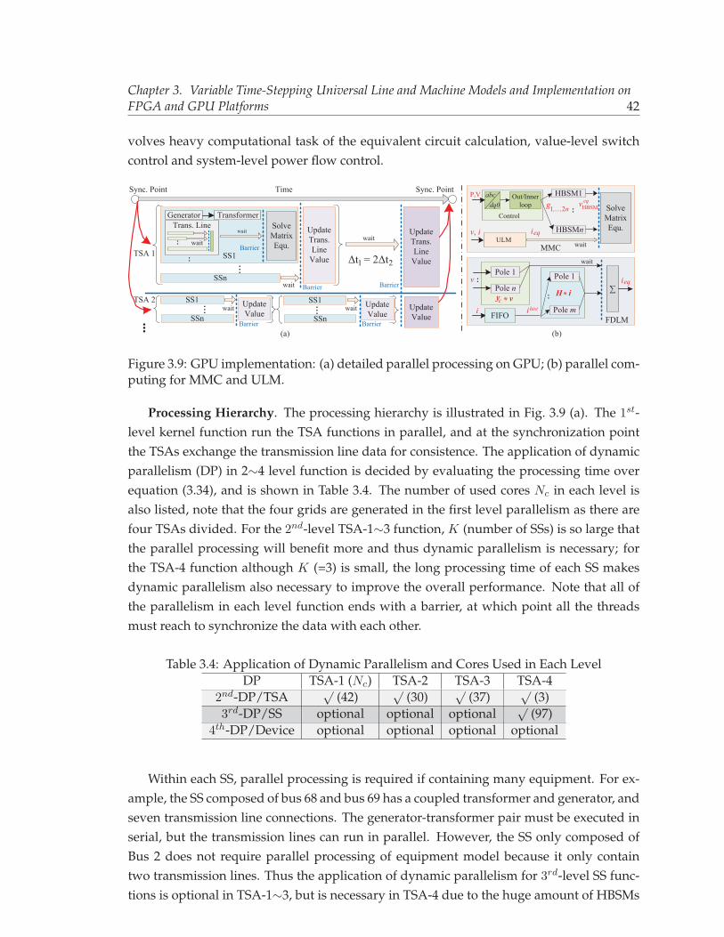
Chapter 3. Variable Time-Stepping Universal Line and Machine Models and Implementation onFPGA and GPU Platforms 42
volves heavy computational task of the equivalent circuit calculation, value-level switchcontrol and system-level power flow control.
...
TSA 1
SSn
UpdateTrans.LineValue
UpdateTrans.LineValue
TSA 2
wait
Barrier Barrier
Sync. Point Sync. PointTime
Generator Transformer
..
Barrier
SolveMatrixEqu.
SS1
UpdateValueSSn
UpdateValue
SS1 ...
wait
wait
Δt = 2Δt1 2
Trans. Line
wait
..
SSn
UpdateValue
SS1
Barrier Barrier(a) (b)
SolveMatrixEqu.
MMC wait
wait wait
...
...
P,V
Control
ULMv, i ieq
HBSM1
HBSMn
g1,...,2n .. vHBSMeq
abcdq0
Out/Innerloop
∑
FDLM
waitPole 1
Pole n
..
FIFO
ieq
yc * v
v ..
i histi
Pole 1
Pole m
.. H* i
Figure 3.9: GPU implementation: (a) detailed parallel processing on GPU; (b) parallel com-puting for MMC and ULM.
Processing Hierarchy. The processing hierarchy is illustrated in Fig. 3.9 (a). The 1st-level kernel function run the TSA functions in parallel, and at the synchronization pointthe TSAs exchange the transmission line data for consistence. The application of dynamicparallelism (DP) in 2∼4 level function is decided by evaluating the processing time overequation (3.34), and is shown in Table 3.4. The number of used cores Nc in each level isalso listed, note that the four grids are generated in the first level parallelism as there arefour TSAs divided. For the 2nd-level TSA-1∼3 function, K (number of SSs) is so large thatthe parallel processing will benefit more and thus dynamic parallelism is necessary; forthe TSA-4 function although K (=3) is small, the long processing time of each SS makesdynamic parallelism also necessary to improve the overall performance. Note that all ofthe parallelism in each level function ends with a barrier, at which point all the threadsmust reach to synchronize the data with each other.
Table 3.4: Application of Dynamic Parallelism and Cores Used in Each LevelDP TSA-1 (Nc) TSA-2 TSA-3 TSA-4
2nd-DP/TSA√
(42)√
(30)√
(37)√
(3)3rd-DP/SS optional optional optional
√(97)
4th-DP/Device optional optional optional optional
Within each SS, parallel processing is required if containing many equipment. For ex-ample, the SS composed of bus 68 and bus 69 has a coupled transformer and generator, andseven transmission line connections. The generator-transformer pair must be executed inserial, but the transmission lines can run in parallel. However, the SS only composed ofBus 2 does not require parallel processing of equipment model because it only containtwo transmission lines. Thus the application of dynamic parallelism for 3rd-level SS func-tions is optional in TSA-1∼3, but is necessary in TSA-4 due to the huge amount of HBSMs
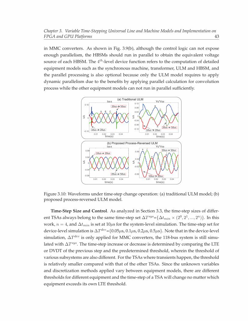
Chapter 3. Variable Time-Stepping Universal Line and Machine Models and Implementation onFPGA and GPU Platforms 43
in MMC converters. As shown in Fig. 3.9(b), although the control logic can not exposeenough parallelism, the HBSMs should run in parallel to obtain the equivalent voltagesource of each HBSM. The 4th-level device function refers to the computation of detailedequipment models such as the synchronous machine, transformer, ULM and HBSM, andthe parallel processing is also optional because only the ULM model requires to applydynamic parallelism due to the benefits by applying parallel calculation for convolutionprocess while the other equipment models can not run in parallel sufficiently.
(a) Traditional ULM
0.01 0.02 0.03 0.04time(s)
-0.10
0
0.10
kA
I39-9
A B C
0.01 0.02 0.03 0.04time(s)
-0.12
-0.08
-0.04
0
0.04
0.08
0.12
kA
Yc*V39
A
BC
10us 20us 10us 20us20us 50us
(b) Proposed Process-Reversed ULM
time(s)
I39-9
0.01 0.02 0.03 0.04time(s)
-0.06
-0.02
0
0.02
0.06
kA
Yc*V39
0.01 0.02 0.03 0.04
-0.08
-0.04
0
0.04
0.08
kA
20us 50usA B C
A
B C
10us 20us
20us 50us
20us 50us
10us 20us
Figure 3.10: Waveforms under time-step change operation: (a) traditional ULM model; (b)proposed process-reversed ULM model.
Time-Step Size and Control. As analyzed in Section 3.3, the time-step sizes of differ-ent TSAs always belong to the same time-step set ΔT sys={Δtmin × (20, 21, ..., 2n)}. In thiswork, n = 4, and Δtmin is set at 10μs for the system-level simulation. The time-step set fordevice-level simulation is ΔT dev={0.05μs, 0.1μs, 0.2μs, 0.5μs}. Note that in the device-levelsimulation, ΔT dev is only applied for MMC converters, the 118-bus system is still simu-lated with ΔT sys. The time-step increase or decrease is determined by comparing the LTEor DVDT of the previous step and the predetermined threshold, wherein the threshold ofvarious subsystems are also different. For the TSAs where transients happen, the thresholdis relatively smaller compared with that of the other TSAs. Since the unknown variablesand discretization methods applied vary between equipment models, there are differentthresholds for different equipment and the time-step of a TSA will change no matter whichequipment exceeds its own LTE threshold.
Chapter 3. Variable Time-Stepping Universal Line and Machine Models and Implementation onFPGA and GPU Platforms 44
3.6 Results and Verification
The two test cases described above were simulated on the FPGA and GPU platform re-spectively and the results are compared with PSCAD/EMTDC� to show the effectivenessof the proposed VTS models. Note that PSCAD/EMTDC� is only a representative of fixedtime-stepping EMT simulation tools, and it does not matter if other software are used forcomparison because the ULM and UM model with fixed time-steps are both commonly-used models. The clock frequency of FPGA boards is set at 100 MHz.
3.6.1 Verification of the ULM Model
Before the ULM model is integrated into the IEEE 39-bus system, it is necessary to verifythe stability of the propose process-reversed method. Note that the UM model in VTS isstable because the state variable remains the same when the time-step changes. To solelyvalidate the proposed ULM model, the subsystem S9 in Fig. 3.6(a) with ideal voltage sourceis simulated while keeping the load and connection with other subsystems as open circuit.At time 0.005s, the time-step changes from 10μs to 20μs; and at time 0.035s, the time-stepchanges from 20μs to 50μs.
The results of i39−9 (from Bus39 to Bus9) and Yc ∗ v39 using the traditional model areshown in Fig. 3.10(a), when the time-step changes, there will have a large oscillation. Sincethe actual state variable changes when the time-step changes, the initial value of the newstate variable will be incorrect, which causes an abrupt change of the convolution results.However, when using the proposed process-reversed model, it can be observed that theconvolution results will remain continuous and stable, which results in a stable currenti39−9 when the time-step changes.
3.6.2 Real-Time Emulation Results of IEEE 39-Bus System on FPGA
To simulate the dynamic behavior of the system, the lightning surge at phase C of trans-mission line L4−14 (between bus 4 and bus 14) and L23−24 is chosen as the transient test.The results are evaluated by the proposed emulator and PSCAD/EMTDC� that used afixed time-step of 10μs while the proposed emulator used adaptive time-steps describedin Section 3.4. The standard 10/350μs lightning surge current [59] is applied in this work,given as:
ILS(t) = CIm(t/τ1)ke−tτ2 /[1 + (t/τ1)
k] (3.35)
where the coefficient C = 1.075, k = 10; the time constant τ1 = 19μs, τ2 = 485μs; the maxi-mum value of the surge current Im = 3kA. The lightning surge current at L4−14 and L23−24is applied at exactly 2s and 2.5s of the simulation to demonstrate the transient behavior ofULM and UM respectively.
First, the simulation is executed in real-time and compared with PSCAD and the hard-ware emulator with fixed time-step (FTS), and the results are recorded in Fig. 3.11. The
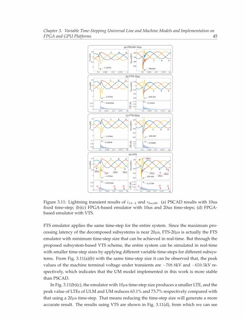
Chapter 3. Variable Time-Stepping Universal Line and Machine Models and Implementation onFPGA and GPU Platforms 45
(a) PSCAD-10us
(s)
(kA)
I14-4
(c) FTS-20us
(s)
(kA)
I14-4
(kV)
Vbus36
(kV)
Vbus36
(s)
LTE(A)
(d) ATS
(s)
(kA)
I14-4
(kV)
Vbus36
LTE(A)
(b) FTS-10us
(s)
(kA)
I14-4
(kV)
V bus36
LTE(A)
2.0 2.005 2.01 2.015
-1
-0.5
0
0.5
-1.232kA
2.5 2.505 2.51 2.515
-500
-300
-100
100
-708.8kV
ABC
ABC
-1
-0.5
0
0.5
2.0 2.005 2.01 2.0150
0.01
0.02 0.02639A
-1.247kA -600
-400
-200
0
200
2.5 2.505 2.51 2.5150
0.040.080.12
(s)
-659.5kV
0.1242A
ABC
ABC
-1
-0.5
0
0.5
2.0 2.005 2.01 2.0150
0.02
0.06
0.1
-1.243kA
0.1003A
-600
-400
-200
0
200
2.5 2.505 2.51 2.5150
0.10.20.3
ABC
ABC
-658.4kV
(s)
0.3368A
-1
-0.5
0
0.5
2.0 2.005 2.01 2.0150
0.01
0.02
-1.252kA
0.02356A
ABC
20us5us 10us 20us
ξ1 ξ2 ξ3
-600
-400
-200
0
200
ABC
-659.4kV
2.5 2.505 2.51 2.5150
0.040.080.12
(s)
40us
10us20us
40us
0.1279Aξ1 ξ2 ξ3
Figure 3.11: Lightning transient results of i14−4 and vbus36. (a) PSCAD results with 10usfixed time-step; (b)(c) FPGA-based emulator with 10us and 20us time-steps; (d) FPGA-based emulator with VTS.
FTS emulator applies the same time-step for the entire system. Since the maximum pro-cessing latency of the decomposed subsystems is near 20μs, FTS-20μs is actually the FTSemulator with minimum time-step size that can be achieved in real-time. But through theproposed subsystem-based VTS scheme, the entire system can be simulated in real-timewith smaller time-step sizes by applying different variable time-steps for different subsys-tems. From Fig. 3.11(a)(b) with the same time-step size it can be observed that, the peakvalues of the machine terminal voltage under transients are −708.8kV and −659.5kV re-spectively, which indicates that the UM model implemented in this work is more stablethan PSCAD.
In Fig. 3.11(b)(c), the emulator with 10μs time-step size produces a smaller LTE, and thepeak value of LTEs of ULM and UM reduces 63.1% and 73.7% respectively compared withthat using a 20μs time-step. That means reducing the time-step size will generate a moreaccurate result. The results using VTS are shown in Fig. 3.11(d), from which we can see
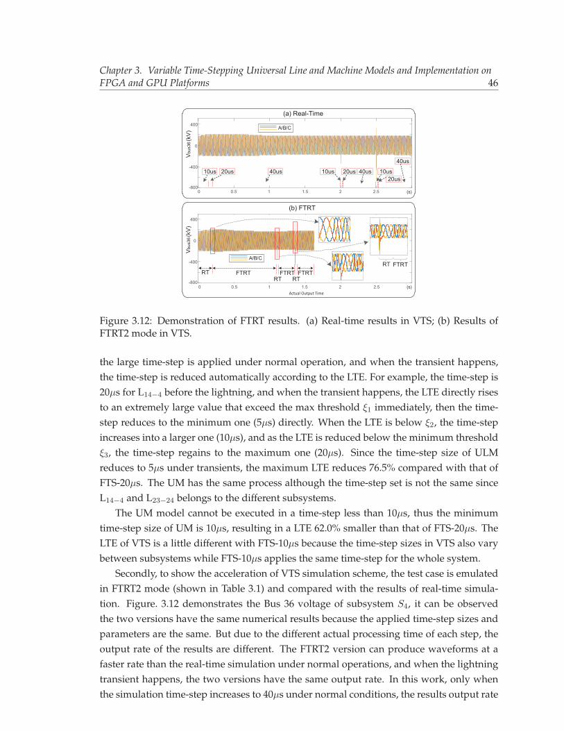
Chapter 3. Variable Time-Stepping Universal Line and Machine Models and Implementation onFPGA and GPU Platforms 46
0 0.5 1 1.5 2 2.5-800
-400
0
400
(a) Real-Time
(kV)
Vbus36
(s)
(b) FTRT
10us 20us 40us 10us 20us 40us 10us
40us
20us
0 0.5 1 1.5 2 2.5-800
-400
0
400
(s)
A/B/C
A/B/C
RT FTRTRT RTFTRT FTRT
(kV)
Vbus36
Actual Output Time
RT FTRT
Figure 3.12: Demonstration of FTRT results. (a) Real-time results in VTS; (b) Results ofFTRT2 mode in VTS.
the large time-step is applied under normal operation, and when the transient happens,the time-step is reduced automatically according to the LTE. For example, the time-step is20μs for L14−4 before the lightning, and when the transient happens, the LTE directly risesto an extremely large value that exceed the max threshold ξ1 immediately, then the time-step reduces to the minimum one (5μs) directly. When the LTE is below ξ2, the time-stepincreases into a larger one (10μs), and as the LTE is reduced below the minimum thresholdξ3, the time-step regains to the maximum one (20μs). Since the time-step size of ULMreduces to 5μs under transients, the maximum LTE reduces 76.5% compared with that ofFTS-20μs. The UM has the same process although the time-step set is not the same sinceL14−4 and L23−24 belongs to the different subsystems.
The UM model cannot be executed in a time-step less than 10μs, thus the minimumtime-step size of UM is 10μs, resulting in a LTE 62.0% smaller than that of FTS-20μs. TheLTE of VTS is a little different with FTS-10μs because the time-step sizes in VTS also varybetween subsystems while FTS-10μs applies the same time-step for the whole system.
Secondly, to show the acceleration of VTS simulation scheme, the test case is emulatedin FTRT2 mode (shown in Table 3.1) and compared with the results of real-time simula-tion. Figure. 3.12 demonstrates the Bus 36 voltage of subsystem S4, it can be observedthe two versions have the same numerical results because the applied time-step sizes andparameters are the same. But due to the different actual processing time of each step, theoutput rate of the results are different. The FTRT2 version can produce waveforms at afaster rate than the real-time simulation under normal operations, and when the lightningtransient happens, the two versions have the same output rate. In this work, only whenthe simulation time-step increases to 40μs under normal conditions, the results output rate
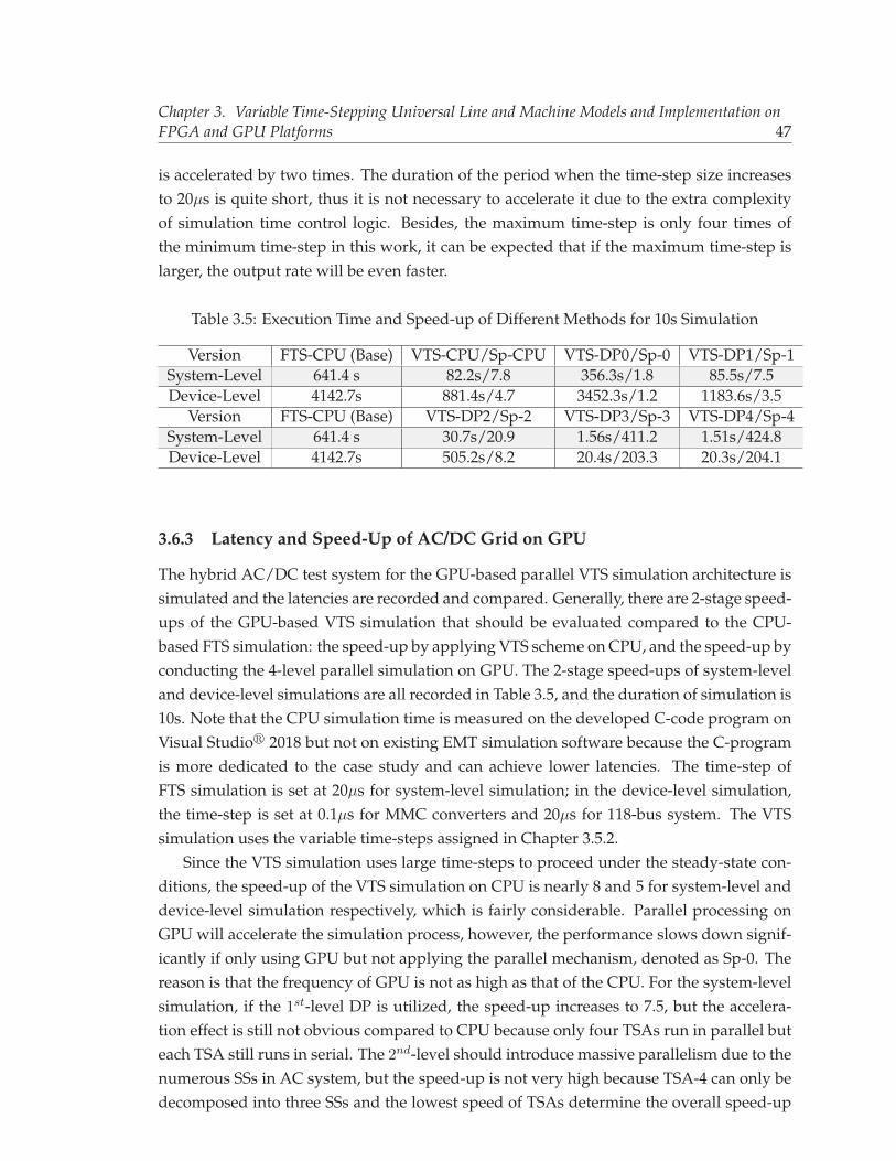
Chapter 3. Variable Time-Stepping Universal Line and Machine Models and Implementation onFPGA and GPU Platforms 47
is accelerated by two times. The duration of the period when the time-step size increasesto 20μs is quite short, thus it is not necessary to accelerate it due to the extra complexityof simulation time control logic. Besides, the maximum time-step is only four times ofthe minimum time-step in this work, it can be expected that if the maximum time-step islarger, the output rate will be even faster.
Table 3.5: Execution Time and Speed-up of Different Methods for 10s Simulation
Version FTS-CPU (Base) VTS-CPU/Sp-CPU VTS-DP0/Sp-0 VTS-DP1/Sp-1System-Level 641.4 s 82.2s/7.8 356.3s/1.8 85.5s/7.5Device-Level 4142.7s 881.4s/4.7 3452.3s/1.2 1183.6s/3.5
Version FTS-CPU (Base) VTS-DP2/Sp-2 VTS-DP3/Sp-3 VTS-DP4/Sp-4System-Level 641.4 s 30.7s/20.9 1.56s/411.2 1.51s/424.8Device-Level 4142.7s 505.2s/8.2 20.4s/203.3 20.3s/204.1
3.6.3 Latency and Speed-Up of AC/DC Grid on GPU
The hybrid AC/DC test system for the GPU-based parallel VTS simulation architecture issimulated and the latencies are recorded and compared. Generally, there are 2-stage speed-ups of the GPU-based VTS simulation that should be evaluated compared to the CPU-based FTS simulation: the speed-up by applying VTS scheme on CPU, and the speed-up byconducting the 4-level parallel simulation on GPU. The 2-stage speed-ups of system-leveland device-level simulations are all recorded in Table 3.5, and the duration of simulation is10s. Note that the CPU simulation time is measured on the developed C-code program onVisual Studio� 2018 but not on existing EMT simulation software because the C-programis more dedicated to the case study and can achieve lower latencies. The time-step ofFTS simulation is set at 20μs for system-level simulation; in the device-level simulation,the time-step is set at 0.1μs for MMC converters and 20μs for 118-bus system. The VTSsimulation uses the variable time-steps assigned in Chapter 3.5.2.
Since the VTS simulation uses large time-steps to proceed under the steady-state con-ditions, the speed-up of the VTS simulation on CPU is nearly 8 and 5 for system-level anddevice-level simulation respectively, which is fairly considerable. Parallel processing onGPU will accelerate the simulation process, however, the performance slows down signif-icantly if only using GPU but not applying the parallel mechanism, denoted as Sp-0. Thereason is that the frequency of GPU is not as high as that of the CPU. For the system-levelsimulation, if the 1st-level DP is utilized, the speed-up increases to 7.5, but the accelera-tion effect is still not obvious compared to CPU because only four TSAs run in parallel buteach TSA still runs in serial. The 2nd-level should introduce massive parallelism due to thenumerous SSs in AC system, but the speed-up is not very high because TSA-4 can only bedecomposed into three SSs and the lowest speed of TSAs determine the overall speed-up
Chapter 3. Variable Time-Stepping Universal Line and Machine Models and Implementation onFPGA and GPU Platforms 48
due to the requirement of synchronization. Once the 3rd-level DP is applied, the speed-upincreases dramatically because of the parallel computation of HBSMs in MMC and devicefunctions in TSA-1∼3. The speed-up by adding the 4th-level DP is not as obvious as the2nd-level and 3rd-level DP, however, it is also necessary to fully exploit the abundant GPUcores.
For device-level simulation, the speed-up is not as large as that of system-level sim-ulation because TSA-4 consumes much more latency than TSA-1∼3 then the speed-upsof TSA-1∼3 can not be revealed in the overall performance. Compared to the FTS sim-ulation on CPU, the overall speed-ups of GPU-based VTS simulation are 424.8 and 204.1respectively for system-level and device-level simulation.
3.7 Summary
In this section, the variable time-stepping universal transmission line model and univer-sal machine model are proposed, and the real-time and faster-than-real-time emulationarchitectures are proposed for FPGA based implementation, while the 4-level parallel sim-ulation architecture is proposed for GPU based implementation. In the proposed ULMmodel, through a novel process-reversal of the traditional model, the stability is signifi-cantly improved during the time-step change operation. By using LTE as the time-stepchange criteria, the time-step can be adjusted properly when the transient happens. Thehardware emulator for large-scale power systems is presented, in which the system is di-vided into small TSAs and each TSA maintains its own time-step set and LTE threshold.By elaborate coordination between TSAs, the faster-than-real-time mode and 4-level parallelVTS simulation can be achieved on FPGA and GPU respectively. The hardware resourcecost, processing delay and speed-ups of test power systems are evaluated, which showsthe practicality of variable time-stepping scheme for EMT simulation.
4Linking-Domain Extraction Decomposition
Method for Parallel Electromagnetic TransientSimulation of AC/DC Networks
Domain decomposition of the network conductance matrix is one of the efficient approachesto solve large-scale networks in parallel. In this work, a novel Linking-Domain Extraction(LDE) based decomposition method is proposed, in which the network matrix is expressedas the sum of a linking-domain matrix (LDM) and a diagonal block matrix (DBM) com-posed of multiple block matrices in diagonal. Through mathematical analysis over LDM,one lemma about the nature of LDM and its proof are proposed. Based on this lemma, thegeneral formulation of the inverse matrix of the sum of LDM and DBM can be found usingthe Woodbury matrix identity, and based on the formulation the network matrix inversioncan be directly computed in parallel to significantly accelerate the matrix inversion pro-cess. Test systems were implemented on both the FPGA and GPU parallel architectures,and the simulation results and speed-ups over the SC method and Gauss-Jordan elimina-tion demonstrate the validity and efficiency of the proposed LDE method.
4.1 Schur Complement Method
The Schur complement (SC) method is one of the representative non-overlapping domaindecomposition methods. Once the network equations have been gathered, the solution ofa linear network reduces to a solution of the linear algebraic system:
G v = ieq (4.1)
The SC method is a non-overlapping method, which means the network conductance
49
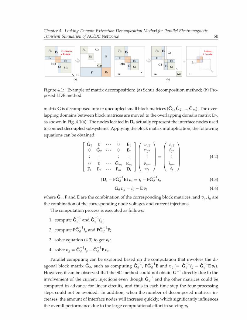
Chapter 4. Linking-Domain Extraction Decomposition Method for Parallel ElectromagneticTransient Simulation of AC/DC Networks 50
G1 E1
F1
G2E2
F2M12
G1
E
F
G2
Dt
...Gm
... G(a)
G1 E1
F1
G2E2
F2M12
Gm...
G
(b)
Gd
+
G1
F1
E1 G1
G2E2
F2
...G2
Gd L
Ls12
...
OverlappingDomain
Linking-Domain
Figure 4.1: Example of matrix decomposition: (a) Schur decomposition method; (b) Pro-posed LDE method.
matrix G is decomposed into m uncoupled small block matrices (G1, G2, ..., Gm). The over-lapping domains between block matrices are moved to the overlapping domain matrix Dt,as shown in Fig. 4.1(a). The nodes located in Dt actually represent the interface nodes usedto connect decoupled subsystems. Applying the block matrix multiplication, the followingequations can be obtained:
⎡⎢⎢⎢⎢⎢⎣
G1 0 · · · 0 E1
0 G2 · · · 0 E2...
......
...0 0 · · · Gm Em
F1 F2 · · · Fm Dt
⎤⎥⎥⎥⎥⎥⎦
⎛⎜⎜⎜⎜⎜⎝
vg1
vg2...
vgm
vt
⎞⎟⎟⎟⎟⎟⎠
=
⎛⎜⎜⎜⎜⎜⎝
ig1ig2...
igmit
⎞⎟⎟⎟⎟⎟⎠
(4.2)
(Dt − FG−1d E) vt = it − FG
−1d ig (4.3)
Gd vg = ig − E vt (4.4)
where Gd, F and E are the combination of the corresponding block matrices, and vg, ig arethe combination of the corresponding node voltages and current injections.
The computation process is executed as follows:
1. compute G−1d and G
−1d ig;
2. compute FG−1d ig and FG
−1d E;
3. solve equation (4.3) to get vt;
4. solve vg = G−1d ig − G
−1d E vt.
Parallel computing can be exploited based on the computation that involves the di-agonal block matrix Gd, such as computing G
−1d , FG
−1d E and vg (= G
−1d ig − G
−1d E vt).
However, it can be observed that the SC method could not obtain G−1 directly due to theinvolvement of the current injections even though G
−1d and the other matrices could be
computed in advance for linear circuits, and thus in each time-step the four processingsteps could not be avoided. In addition, when the number of decomposed matrices in-creases, the amount of interface nodes will increase quickly, which significantly influencesthe overall performance due to the large computational effort in solving vt.
Chapter 4. Linking-Domain Extraction Decomposition Method for Parallel ElectromagneticTransient Simulation of AC/DC Networks 51
4.2 Proposed Linking-Domain Extraction based DecompositionMethod
Focusing on the overlapping domain between subsystems, the linking-domain matrix isdefined and extracted from the original network matrix. Through mathematical analysisover the linking-domain matrix, an important lemma is put forward, based on which theinverse matrix of the network matrix can be computed in parallel.
4.2.1 LDE Matrix Decomposition
Different from the logic of the SC method that operates on the decomposition of the orig-inal conductance matrix, the proposed LDE method decomposes the original matrix intotwo separate matrices: the diagonal block matrix Gd and the linking-domain matrix L.
G = Gd + L (4.5)
As shown in Fig. 4.1(b), the sizes of the decomposed block matrices (G1,G2, ...,Gm) arelarger than using the SC method, because in the SC method all the overlapping areas andtheir corresponding rows and columns are removed from the block matrices, while in theLDE method only the linking-domain matrix is extracted from the original matrix and thesize of each block matrix does not decrease. Note that the linking-domain has a differentmeaning from the overlapping domain, because the elements in the overlapping domainactually are the sum of the corresponding values in the linking-domain matrix and theblock matrices, as marked in Fig. 4.1.
The construction of L matrix is as follows: let the linking-domain matrix contain a smallmatrix with non-zero diagonal elements (Ls) and the other all-zero matrices, as illustratedin Fig. 4.1(b). The location of Ls is the same as the overlapping domain in G and thesize of Ls is (n1 + n2) × (n1 + n2), where n1 is the number of interface nodes belongingto the first subsystem and n2 is the number of interface nodes belonging to the secondsubsystem (taking two decomposed subsystems as an example). Ls can be regarded as thecombination of four block matrices: the top left block matrix and the bottom right blockmatrix are both diagonal matrices, and the top right and bottom left block matrices aretranspose of each other. The top right (n1×n2) and bottom left (n2×n1) block matrices arethe same as those of the overlapping domain matrix, and after the two parts are assigned,the diagonal elements in the top left (n1 × n1) and bottom right (n2 × n2) block matrix are
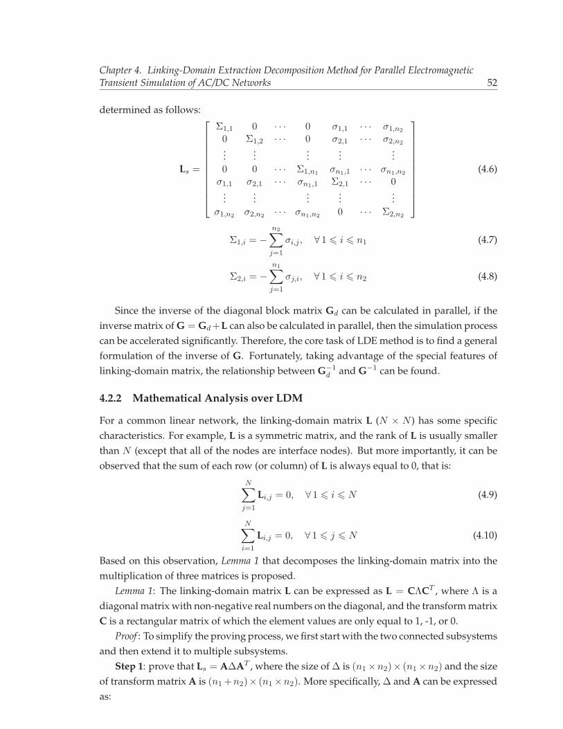
Chapter 4. Linking-Domain Extraction Decomposition Method for Parallel ElectromagneticTransient Simulation of AC/DC Networks 52
determined as follows:
Ls =
⎡⎢⎢⎢⎢⎢⎢⎢⎢⎢⎢⎣
Σ1,1 0 · · · 0 σ1,1 · · · σ1,n2
0 Σ1,2 · · · 0 σ2,1 · · · σ2,n2
......
......
...0 0 · · · Σ1,n1 σn1,1 · · · σn1,n2
σ1,1 σ2,1 · · · σn1,1 Σ2,1 · · · 0...
......
......
σ1,n2 σ2,n2 · · · σn1,n2 0 · · · Σ2,n2
⎤⎥⎥⎥⎥⎥⎥⎥⎥⎥⎥⎦
(4.6)
Σ1,i = −n2∑j=1
σi,j , ∀ 1 � i � n1 (4.7)
Σ2,i = −n1∑j=1
σj,i, ∀ 1 � i � n2 (4.8)
Since the inverse of the diagonal block matrix Gd can be calculated in parallel, if theinverse matrix of G = Gd+L can also be calculated in parallel, then the simulation processcan be accelerated significantly. Therefore, the core task of LDE method is to find a generalformulation of the inverse of G. Fortunately, taking advantage of the special features oflinking-domain matrix, the relationship between G−1
d and G−1 can be found.
4.2.2 Mathematical Analysis over LDM
For a common linear network, the linking-domain matrix L (N × N ) has some specificcharacteristics. For example, L is a symmetric matrix, and the rank of L is usually smallerthan N (except that all of the nodes are interface nodes). But more importantly, it can beobserved that the sum of each row (or column) of L is always equal to 0, that is:
N∑j=1
Li,j = 0, ∀ 1 � i � N (4.9)
N∑i=1
Li,j = 0, ∀ 1 � j � N (4.10)
Based on this observation, Lemma 1 that decomposes the linking-domain matrix into themultiplication of three matrices is proposed.
Lemma 1: The linking-domain matrix L can be expressed as L = CΛCT , where Λ is adiagonal matrix with non-negative real numbers on the diagonal, and the transform matrixC is a rectangular matrix of which the element values are only equal to 1, -1, or 0.
Proof : To simplify the proving process, we first start with the two connected subsystemsand then extend it to multiple subsystems.
Step 1: prove that Ls = AΔAT , where the size of Δ is (n1×n2)× (n1×n2) and the sizeof transform matrix A is (n1+n2)× (n1×n2). More specifically, Δ and A can be expressedas:
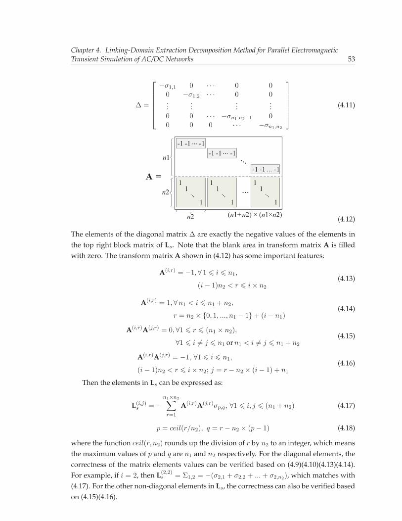
Chapter 4. Linking-Domain Extraction Decomposition Method for Parallel ElectromagneticTransient Simulation of AC/DC Networks 53
Δ =
⎡⎢⎢⎢⎢⎢⎣
−σ1,1 0 · · · 0 00 −σ1,2 · · · 0 0...
......
...0 0 · · · −σn1,n2−1 00 0 0 · · · −σn1,n2
⎤⎥⎥⎥⎥⎥⎦
(4.11)
A =1
...1
1
(n1+n2) × (n1×n2)
1...
1
1
1...
1
1...
n2
n2
n1
-1 -1 -1...-1 -1-1 ...
-1 -1 ... -1...
(4.12)
The elements of the diagonal matrix Δ are exactly the negative values of the elements inthe top right block matrix of Ls. Note that the blank area in transform matrix A is filledwith zero. The transform matrix A shown in (4.12) has some important features:
A(i,r) = −1, ∀ 1 � i � n1,
(i− 1)n2 < r � i× n2
(4.13)
A(i,r) = 1, ∀n1 < i � n1 + n2,
r = n2 × {0, 1, ..., n1 − 1}+ (i− n1)(4.14)
A(i,r)A(j,r) = 0, ∀1 � r � (n1 × n2),
∀1 � i �= j � n1 orn1 < i �= j � n1 + n2
(4.15)
A(i,r)A(j,r) = −1, ∀1 � i � n1,
(i− 1)n2 < r � i× n2; j = r − n2 × (i− 1) + n1
(4.16)
Then the elements in Ls can be expressed as:
L(i,j)s = −
n1×n2∑r=1
A(i,r)A(j,r)σp,q, ∀1 � i, j � (n1 + n2) (4.17)
p = ceil(r/n2), q = r − n2 × (p− 1) (4.18)
where the function ceil(r, n2) rounds up the division of r by n2 to an integer, which meansthe maximum values of p and q are n1 and n2 respectively. For the diagonal elements, thecorrectness of the matrix elements values can be verified based on (4.9)(4.10)(4.13)(4.14).For example, if i = 2, then L(2,2)
s = Σ1,2 = −(σ2,1 + σ2,2 + ... + σ2,n2), which matches with(4.17). For the other non-diagonal elements in Ls, the correctness can also be verified basedon (4.15)(4.16).
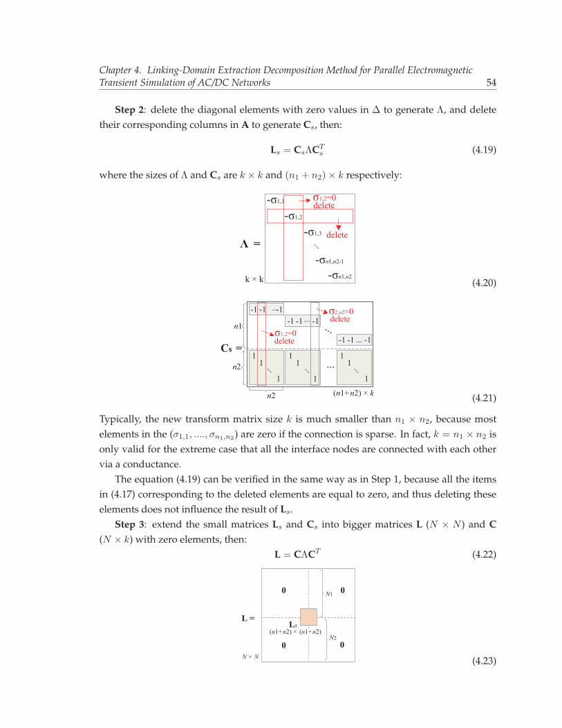
Chapter 4. Linking-Domain Extraction Decomposition Method for Parallel ElectromagneticTransient Simulation of AC/DC Networks 54
Step 2: delete the diagonal elements with zero values in Δ to generate Λ, and deletetheir corresponding columns in A to generate Cs, then:
Ls = CsΛCTs (4.19)
where the sizes of Λ and Cs are k × k and (n1 + n2)× k respectively:
Λ =
-σ1,1
...
k × k
-σ1,2
-σ1,3
-σn1,n2-1-σn1,n2
deleteσ1,2=0
delete
(4.20)
Cs =1
...1
1
(n1+n2) × k
1...
1
1
1...
1
1...
n2
n2
n1
-1 -1 -1...-1 -1-1 ...
-1 -1 ... -1...
deleteσ1,2=0
deleteσ2,n2=0
(4.21)
Typically, the new transform matrix size k is much smaller than n1 × n2, because mostelements in the (σ1,1, ...., σn1,n2) are zero if the connection is sparse. In fact, k = n1 × n2 isonly valid for the extreme case that all the interface nodes are connected with each othervia a conductance.
The equation (4.19) can be verified in the same way as in Step 1, because all the itemsin (4.17) corresponding to the deleted elements are equal to zero, and thus deleting theseelements does not influence the result of Ls.
Step 3: extend the small matrices Ls and Cs into bigger matrices L (N × N ) and C(N × k) with zero elements, then:
L = CΛCT (4.22)
L =Ls
0 0
0 0N × N
(n1+n2) × (n1+n2)
N1
N2
(4.23)
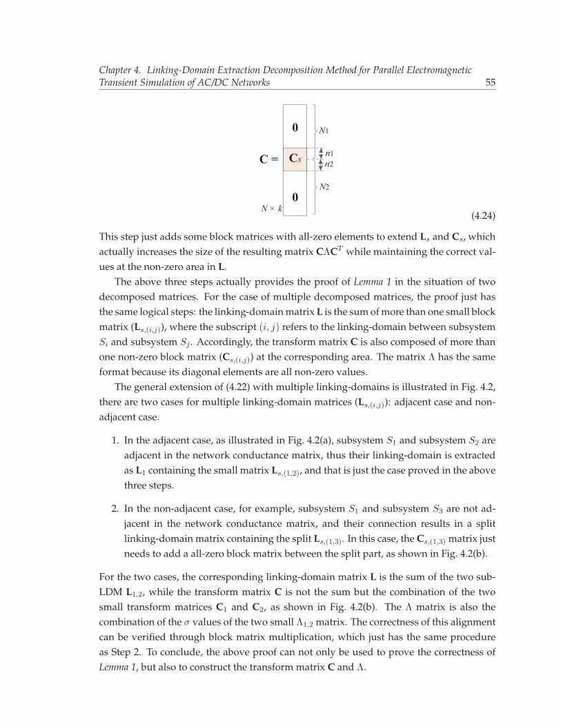
Chapter 4. Linking-Domain Extraction Decomposition Method for Parallel ElectromagneticTransient Simulation of AC/DC Networks 55
C = Cs
0
0N × k
N1
N2
n1n2
(4.24)
This step just adds some block matrices with all-zero elements to extend Ls and Cs, whichactually increases the size of the resulting matrix CΛCT while maintaining the correct val-ues at the non-zero area in L.
The above three steps actually provides the proof of Lemma 1 in the situation of twodecomposed matrices. For the case of multiple decomposed matrices, the proof just hasthe same logical steps: the linking-domain matrix L is the sum of more than one small blockmatrix (Ls,(i,j)), where the subscript (i, j) refers to the linking-domain between subsystemSi and subsystem Sj . Accordingly, the transform matrix C is also composed of more thanone non-zero block matrix (Cs,(i,j)) at the corresponding area. The matrix Λ has the sameformat because its diagonal elements are all non-zero values.
The general extension of (4.22) with multiple linking-domains is illustrated in Fig. 4.2,there are two cases for multiple linking-domain matrices (Ls,(i,j)): adjacent case and non-adjacent case.
1. In the adjacent case, as illustrated in Fig. 4.2(a), subsystem S1 and subsystem S2 areadjacent in the network conductance matrix, thus their linking-domain is extractedas L1 containing the small matrix Ls,(1,2), and that is just the case proved in the abovethree steps.
2. In the non-adjacent case, for example, subsystem S1 and subsystem S3 are not ad-jacent in the network conductance matrix, and their connection results in a splitlinking-domain matrix containing the split Ls,(1,3). In this case, the Cs,(1,3) matrix justneeds to add a all-zero block matrix between the split part, as shown in Fig. 4.2(b).
For the two cases, the corresponding linking-domain matrix L is the sum of the two sub-LDM L1,2, while the transform matrix C is not the sum but the combination of the twosmall transform matrices C1 and C2, as shown in Fig. 4.2(b). The Λ matrix is also thecombination of the σ values of the two small Λ1,2 matrix. The correctness of this alignmentcan be verified through block matrix multiplication, which just has the same procedureas Step 2. To conclude, the above proof can not only be used to prove the correctness ofLemma 1, but also to construct the transform matrix C and Λ.
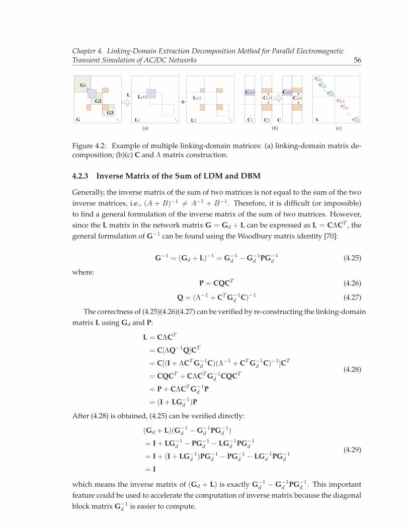
Chapter 4. Linking-Domain Extraction Decomposition Method for Parallel ElectromagneticTransient Simulation of AC/DC Networks 56
(a)
L+
G1
...
G2
G
Ls12 Ls13
...G3
...L1 L2
Cs12Cs13
C(b)
C1 C2
Cs12Cs13
Λ
σ
σσ
σ
...
...
σ
σ
s12s12
s12
s13
s13
s13
1
2
k1
k2
2
1
(c)
Figure 4.2: Example of multiple linking-domain matrices: (a) linking-domain matrix de-composition; (b)(c) C and Λ matrix construction.
4.2.3 Inverse Matrix of the Sum of LDM and DBM
Generally, the inverse matrix of the sum of two matrices is not equal to the sum of the twoinverse matrices, i.e., (A + B)−1 �= A−1 + B−1. Therefore, it is difficult (or impossible)to find a general formulation of the inverse matrix of the sum of two matrices. However,since the L matrix in the network matrix G = Gd + L can be expressed as L = CΛCT , thegeneral formulation of G−1 can be found using the Woodbury matrix identity [70]:
G−1 = (Gd + L)−1 = G−1d − G−1
d PG−1d (4.25)
where:P = CQCT (4.26)
Q = (Λ−1 + CT G−1d C)−1 (4.27)
The correctness of (4.25)(4.26)(4.27) can be verified by re-constructing the linking-domainmatrix L using Gd and P:
L = CΛCT
= C[ΛQ−1Q]CT
= C[(I + ΛCT G−1d C)(Λ−1 + CT G−1
d C)−1]CT
= CQCT + CΛCT G−1d CQCT
= P + CΛCT G−1d P
= (I + LG−1d )P
(4.28)
After (4.28) is obtained, (4.25) can be verified directly:
(Gd + L)(G−1d − G−1
d PG−1d )
= I + LG−1d − PG−1
d − LG−1d PG−1
d
= I + (I + LG−1d )PG−1
d − PG−1d − LG−1
d PG−1d
= I
(4.29)
which means the inverse matrix of (Gd + L) is exactly G−1d − G−1
d PG−1d . This important
feature could be used to accelerate the computation of inverse matrix because the diagonalblock matrix G−1
d is easier to compute.
Chapter 4. Linking-Domain Extraction Decomposition Method for Parallel ElectromagneticTransient Simulation of AC/DC Networks 57
4.2.4 Parallel Computation Using LDE
Based on (4.25), computing the inverse matrix of G actually only needs to know the valueof G−1
d , because the diagonal elements of Λ−1 are just reciprocals of those of Λ, and C isconstant once the network circuit topology is determined. Since Gd is a diagonal blockmatrix, the inverse matrix of its block sub-matrices on the diagonal can be computed inparallel. As suggested by (4.25)(4.26)(4.27), P = CQCT should be calculated first andthen G−1
d PG−1d is computed; however, this procedure may be not efficient because the
size of P is N × N , which increases the size of Q and improves the complexity of matrixmultiplication. It is suggested that T = G−1
d C is computed first and then computing TQTT .Because generally the block matrices in Gd is symmetric, which means G−1
d is symmetric,then:
(G−1d C)T = CT (G−1
d )T = CT G−1d = TT (4.30)
Besides, based on the special feature of transformation matrix C, T = G−1d C could be
obtained directly even without multiplication operations. Therefore, the parallel matrixinversion procedure can be performed as follows:
1. compute G−1d and Λ−1;
2. compute Q = (Λ−1 + CT G−1d C)−1;
3. compute T = G−1d C and TQTT ;
4. compute G−1 = G−1d − TQTT .
Complexity analysis: For the first step, the computation of the inverse matrix can be ex-ecuted in parallel with a computational complexity of O(N3
j ), where Nj is the maximumsize of the diagonal block matrices. For the second step, since the transform matrix C isalready known and only contains +1, -1, or 0, the elements in CT G−1
d C actually can beobtained from G−1
d with only plus or minus operations. This means, Q−1 can be obtainedwithout multiplication operations after the first step. Then the computational complexityof computing Q is O(k3). For the third step, the complexity is determined by the compu-tation of TQTT , which depends on the parallel technique applied to calculate the matrixmultiplication. If the matrix multiplications run in parallel for each block matrix, the com-plexity will be O(N3
j ); if the matrix multiplication run in massively parallel fashion foreach row and each column, then the complexity is O(N2
j ). Thus the total complexity of theLDE method is O(N3
j +k3) if block-based parallel processing is exploited for the third step.
4.2.5 Advantages and Limitations of LDE
Compared to the SC method that requires the information of the equivalent current injec-tions, the biggest advantage of the LDE method is that it does not need to know the righthand side of the network matrix equation, because it could directly compute the inverse
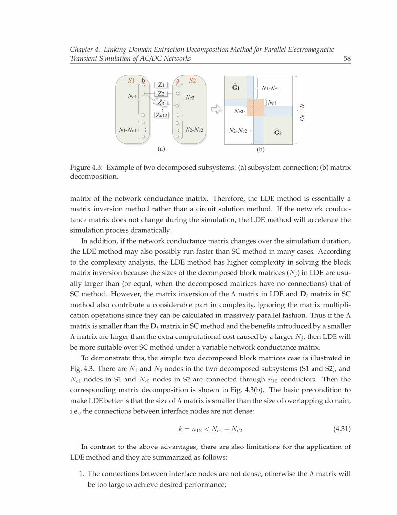
Chapter 4. Linking-Domain Extraction Decomposition Method for Parallel ElectromagneticTransient Simulation of AC/DC Networks 58
G1
G2
(a)
Z1Z2
Zn12
...
Nc1
...N1-Nc1
S1
Nc2
N2-Nc2
Z3
...
S2
N1+N2
N1-Nc1
Nc1Nc2
N2-Nc2
(b)
ab
Figure 4.3: Example of two decomposed subsystems: (a) subsystem connection; (b) matrixdecomposition.
matrix of the network conductance matrix. Therefore, the LDE method is essentially amatrix inversion method rather than a circuit solution method. If the network conduc-tance matrix does not change during the simulation, the LDE method will accelerate thesimulation process dramatically.
In addition, if the network conductance matrix changes over the simulation duration,the LDE method may also possibly run faster than SC method in many cases. Accordingto the complexity analysis, the LDE method has higher complexity in solving the blockmatrix inversion because the sizes of the decomposed block matrices (Nj) in LDE are usu-ally larger than (or equal, when the decomposed matrices have no connections) that ofSC method. However, the matrix inversion of the Λ matrix in LDE and Dt matrix in SCmethod also contribute a considerable part in complexity, ignoring the matrix multipli-cation operations since they can be calculated in massively parallel fashion. Thus if the Λ
matrix is smaller than the Dt matrix in SC method and the benefits introduced by a smallerΛ matrix are larger than the extra computational cost caused by a larger Nj , then LDE willbe more suitable over SC method under a variable network conductance matrix.
To demonstrate this, the simple two decomposed block matrices case is illustrated inFig. 4.3. There are N1 and N2 nodes in the two decomposed subsystems (S1 and S2), andNc1 nodes in S1 and Nc2 nodes in S2 are connected through n12 conductors. Then thecorresponding matrix decomposition is shown in Fig. 4.3(b). The basic precondition tomake LDE better is that the size of Λ matrix is smaller than the size of overlapping domain,i.e., the connections between interface nodes are not dense:
k = n12 < Nc1 +Nc2 (4.31)
In contrast to the above advantages, there are also limitations for the application ofLDE method and they are summarized as follows:
1. The connections between interface nodes are not dense, otherwise the Λ matrix willbe too large to achieve desired performance;
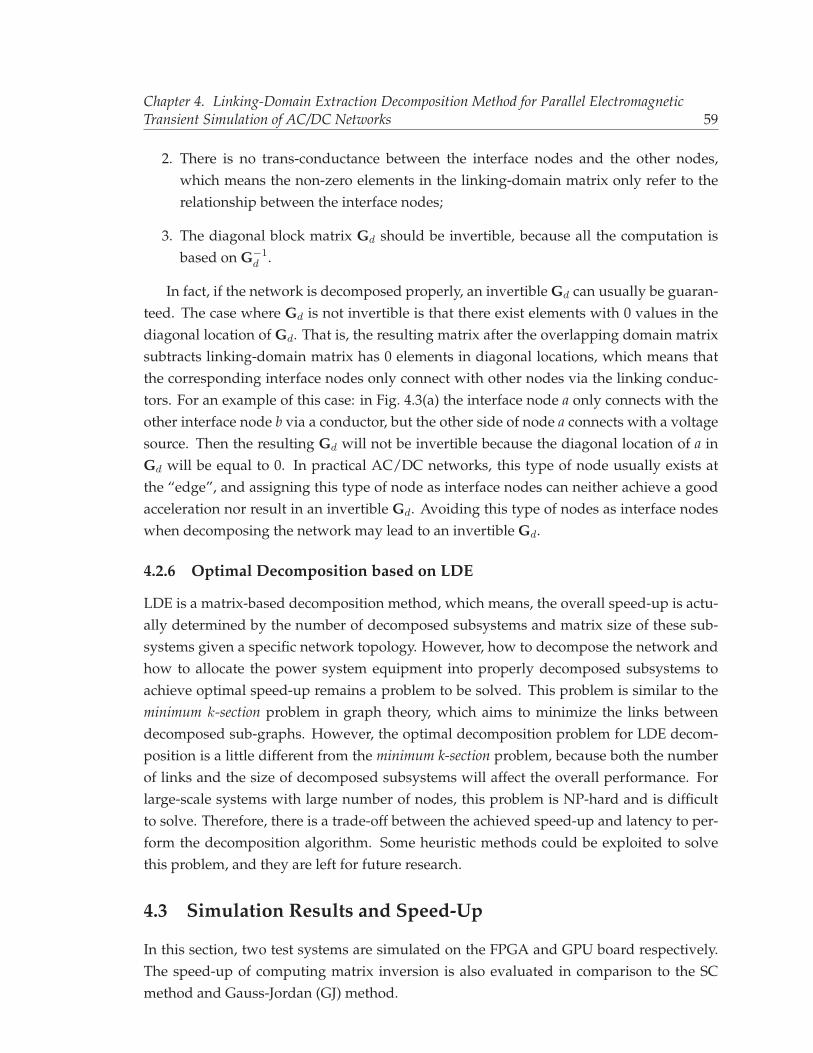
Chapter 4. Linking-Domain Extraction Decomposition Method for Parallel ElectromagneticTransient Simulation of AC/DC Networks 59
2. There is no trans-conductance between the interface nodes and the other nodes,which means the non-zero elements in the linking-domain matrix only refer to therelationship between the interface nodes;
3. The diagonal block matrix Gd should be invertible, because all the computation isbased on G−1
d .
In fact, if the network is decomposed properly, an invertible Gd can usually be guaran-teed. The case where Gd is not invertible is that there exist elements with 0 values in thediagonal location of Gd. That is, the resulting matrix after the overlapping domain matrixsubtracts linking-domain matrix has 0 elements in diagonal locations, which means thatthe corresponding interface nodes only connect with other nodes via the linking conduc-tors. For an example of this case: in Fig. 4.3(a) the interface node a only connects with theother interface node b via a conductor, but the other side of node a connects with a voltagesource. Then the resulting Gd will not be invertible because the diagonal location of a inGd will be equal to 0. In practical AC/DC networks, this type of node usually exists atthe “edge”, and assigning this type of node as interface nodes can neither achieve a goodacceleration nor result in an invertible Gd. Avoiding this type of nodes as interface nodeswhen decomposing the network may lead to an invertible Gd.
4.2.6 Optimal Decomposition based on LDE
LDE is a matrix-based decomposition method, which means, the overall speed-up is actu-ally determined by the number of decomposed subsystems and matrix size of these sub-systems given a specific network topology. However, how to decompose the network andhow to allocate the power system equipment into properly decomposed subsystems toachieve optimal speed-up remains a problem to be solved. This problem is similar to theminimum k-section problem in graph theory, which aims to minimize the links betweendecomposed sub-graphs. However, the optimal decomposition problem for LDE decom-position is a little different from the minimum k-section problem, because both the numberof links and the size of decomposed subsystems will affect the overall performance. Forlarge-scale systems with large number of nodes, this problem is NP-hard and is difficultto solve. Therefore, there is a trade-off between the achieved speed-up and latency to per-form the decomposition algorithm. Some heuristic methods could be exploited to solvethis problem, and they are left for future research.
4.3 Simulation Results and Speed-Up
In this section, two test systems are simulated on the FPGA and GPU board respectively.The speed-up of computing matrix inversion is also evaluated in comparison to the SCmethod and Gauss-Jordan (GJ) method.
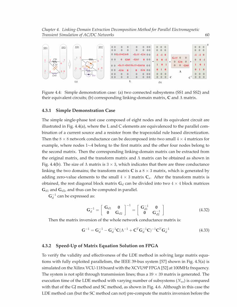
Chapter 4. Linking-Domain Extraction Decomposition Method for Parallel ElectromagneticTransient Simulation of AC/DC Networks 60
1
2
3
4
6
5
L45
r36
C35
Il45
Gl45
Ic35
Gc35
Gc35
L
G36+ 0
Gl450
-Gc35 -G36
0-Gl45
-Gl45-Gc35
-G36 0
Gc35
G36
+Gl45 0
0
00
00
0
0 0 0 0 0 0 0 0
00
0
00
0000
00
-1 -1 0
0 0 -1
1 0 1
0 1 0
C
=
0 0 00 0 0
0 0 00 0 0
×Gc35
G36Gl45
0 00
000
Λ
-1 -1 0
0 0 -1
1 0 1
0 1 0
C0 0 00 0 0
0 0 00 0 0
T
T
×
(a) (b)
0 0 0 0 0 0 0 0
0 0 0 0 0 0 0 00 0 0 0 0 0 0 0
1
2
7
8
3
4
7
8
6
5
SS1 SS2 SS1 SS2
Figure 4.4: Simple demonstration case: (a) two connected subsystems (SS1 and SS2) andtheir equivalent circuits; (b) corresponding linking-domain matrix, C and Λ matrix.
4.3.1 Simple Demonstration Case
The simple single-phase test case composed of eight nodes and its equivalent circuit areillustrated in Fig. 4.4(a), where the L and C elements are equivalenced to the parallel com-bination of a current source and a resistor from the trapezoidal rule based dircretization.Then the 8× 8 network conductance can be decomposed into two small 4× 4 matrices forexample, where nodes 1∼4 belong to the first matrix and the other four nodes belong tothe second matrix. Then the corresponding linking-domain matrix can be extracted fromthe original matrix, and the transform matrix and Λ matrix can be obtained as shown inFig. 4.4(b). The size of Λ matrix is 3 × 3, which indicates that there are three conductancelinking the two domains; the transform matrix C is a 8 × 3 matrix, which is generated byadding zero-value elements to the small 4 × 3 matrix Cs. After the transform matrix isobtained, the rest diagonal block matrix Gd can be divided into two 4 × 4 block matricesGd1 and Gd2, and thus can be computed in parallel.
G−1d can be expressed as:
G−1d =
[Gd1 0
0 Gd2
]−1=
[G−1
d1 00 G−1
d2
](4.32)
Then the matrix inversion of the whole network conductance matrix is:
G−1 = G−1d − G−1
d C(Λ−1 + CT G−1d C)−1CT G−1
d (4.33)
4.3.2 Speed-Up of Matrix Equation Solution on FPGA
To verify the validity and effectiveness of the LDE method in solving large matrix equa-tions with fully exploited parallelism, the IEEE 39-bus system [57] shown in Fig. 4.5(a) issimulated on the Xilinx VCU-118 board with the XCVU9P FPGA [52] at 100MHz frequency.The system is not split through transmission lines; thus a 39× 39 matrix is generated. Theexecution time of the LDE method with varying number of subsystems (Nss) is comparedwith that of the GJ method and SC method, as shown in Fig. 4.6. Although in this case theLDE method can (but the SC method can not) pre-compute the matrix inversion before the
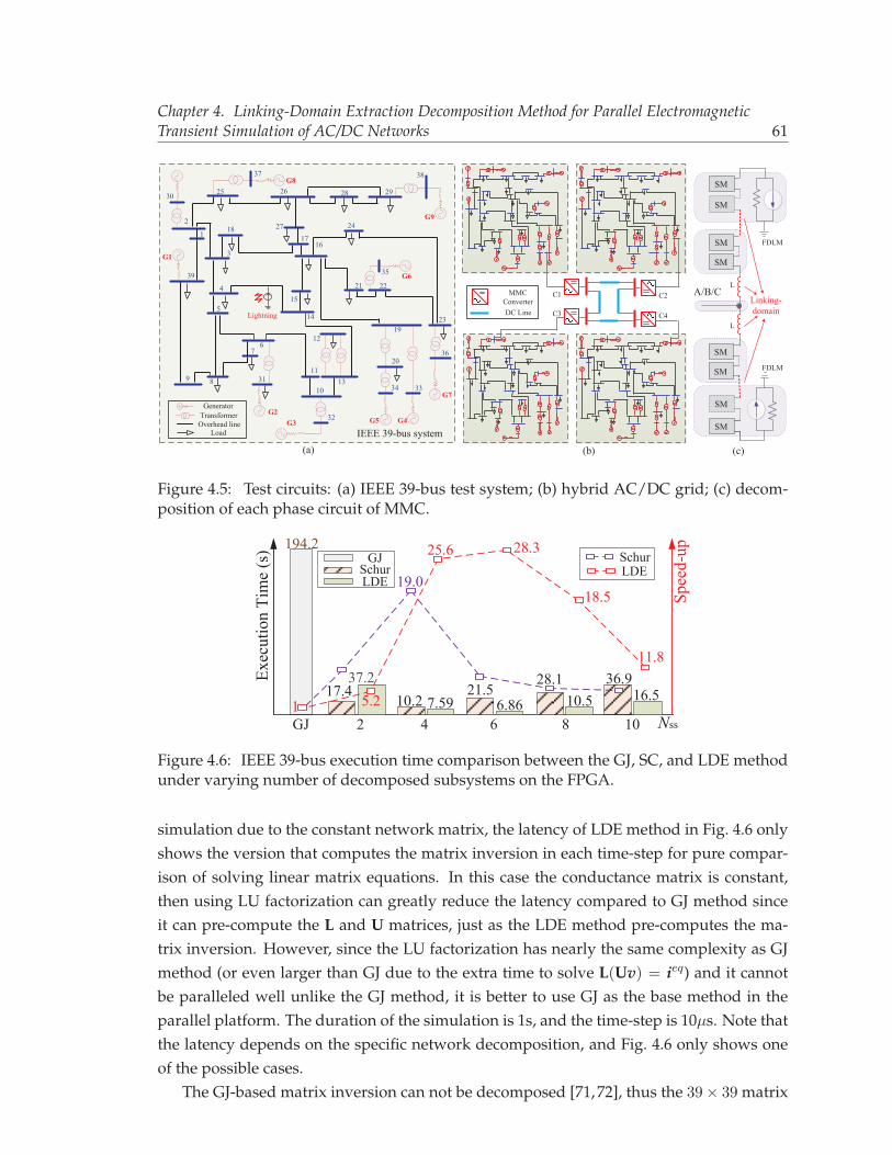
Chapter 4. Linking-Domain Extraction Decomposition Method for Parallel ElectromagneticTransient Simulation of AC/DC Networks 61
C1
C4C3
C2
37
25
2
1
30
39
9 8
76
5
4
3110
11
12
13
15
163
1817
26
27
28 29
24
19
20
32
34 33
21 22
35
23
36
38
14
IEEE 39-bus systemOverhead line
Generator
Load
Transformer
G8
G9
G1
G2G3
G7
G5 G4
G6
Lightning
(a) (b)
MMCConverterDC Line
(c)
SM
SM
SM
SM
SM
A/B/C
FDLM
FDLM
L
L
SM
SM
SM
Linking-domain
Figure 4.5: Test circuits: (a) IEEE 39-bus test system; (b) hybrid AC/DC grid; (c) decom-position of each phase circuit of MMC.
37.2
NssGJ
ExecutionTime(s)
4
194.2
7.59 6.86
GJ
LDE
Speed-up
210.5 16.5
1 5.2
25.6 28.3
18.5
11.8
6 8 10
17.410.2
21.528.1 36.9
Schur19.0
LDESchur
Figure 4.6: IEEE 39-bus execution time comparison between the GJ, SC, and LDE methodunder varying number of decomposed subsystems on the FPGA.
simulation due to the constant network matrix, the latency of LDE method in Fig. 4.6 onlyshows the version that computes the matrix inversion in each time-step for pure compar-ison of solving linear matrix equations. In this case the conductance matrix is constant,then using LU factorization can greatly reduce the latency compared to GJ method sinceit can pre-compute the L and U matrices, just as the LDE method pre-computes the ma-trix inversion. However, since the LU factorization has nearly the same complexity as GJmethod (or even larger than GJ due to the extra time to solve L(Uv) = ieq) and it cannotbe paralleled well unlike the GJ method, it is better to use GJ as the base method in theparallel platform. The duration of the simulation is 1s, and the time-step is 10μs. Note thatthe latency depends on the specific network decomposition, and Fig. 4.6 only shows oneof the possible cases.
The GJ-based matrix inversion can not be decomposed [71,72], thus the 39× 39 matrix
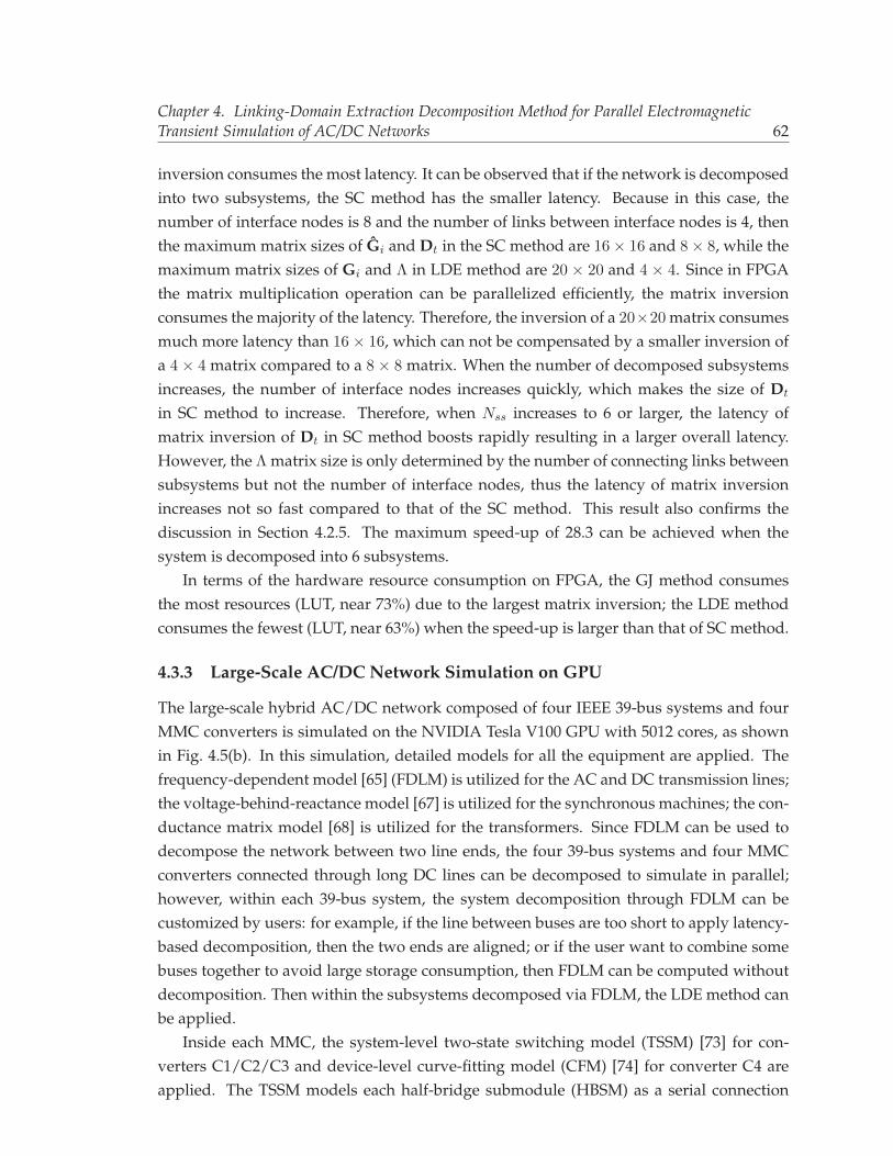
Chapter 4. Linking-Domain Extraction Decomposition Method for Parallel ElectromagneticTransient Simulation of AC/DC Networks 62
inversion consumes the most latency. It can be observed that if the network is decomposedinto two subsystems, the SC method has the smaller latency. Because in this case, thenumber of interface nodes is 8 and the number of links between interface nodes is 4, thenthe maximum matrix sizes of Gi and Dt in the SC method are 16× 16 and 8× 8, while themaximum matrix sizes of Gi and Λ in LDE method are 20 × 20 and 4 × 4. Since in FPGAthe matrix multiplication operation can be parallelized efficiently, the matrix inversionconsumes the majority of the latency. Therefore, the inversion of a 20×20 matrix consumesmuch more latency than 16× 16, which can not be compensated by a smaller inversion ofa 4 × 4 matrix compared to a 8 × 8 matrix. When the number of decomposed subsystemsincreases, the number of interface nodes increases quickly, which makes the size of Dt
in SC method to increase. Therefore, when Nss increases to 6 or larger, the latency ofmatrix inversion of Dt in SC method boosts rapidly resulting in a larger overall latency.However, the Λ matrix size is only determined by the number of connecting links betweensubsystems but not the number of interface nodes, thus the latency of matrix inversionincreases not so fast compared to that of the SC method. This result also confirms thediscussion in Section 4.2.5. The maximum speed-up of 28.3 can be achieved when thesystem is decomposed into 6 subsystems.
In terms of the hardware resource consumption on FPGA, the GJ method consumesthe most resources (LUT, near 73%) due to the largest matrix inversion; the LDE methodconsumes the fewest (LUT, near 63%) when the speed-up is larger than that of SC method.
4.3.3 Large-Scale AC/DC Network Simulation on GPU
The large-scale hybrid AC/DC network composed of four IEEE 39-bus systems and fourMMC converters is simulated on the NVIDIA Tesla V100 GPU with 5012 cores, as shownin Fig. 4.5(b). In this simulation, detailed models for all the equipment are applied. Thefrequency-dependent model [65] (FDLM) is utilized for the AC and DC transmission lines;the voltage-behind-reactance model [67] is utilized for the synchronous machines; the con-ductance matrix model [68] is utilized for the transformers. Since FDLM can be used todecompose the network between two line ends, the four 39-bus systems and four MMCconverters connected through long DC lines can be decomposed to simulate in parallel;however, within each 39-bus system, the system decomposition through FDLM can becustomized by users: for example, if the line between buses are too short to apply latency-based decomposition, then the two ends are aligned; or if the user want to combine somebuses together to avoid large storage consumption, then FDLM can be computed withoutdecomposition. Then within the subsystems decomposed via FDLM, the LDE method canbe applied.
Inside each MMC, the system-level two-state switching model (TSSM) [73] for con-verters C1/C2/C3 and device-level curve-fitting model (CFM) [74] for converter C4 areapplied. The TSSM models each half-bridge submodule (HBSM) as a serial connection
Chapter 4. Linking-Domain Extraction Decomposition Method for Parallel ElectromagneticTransient Simulation of AC/DC Networks 63
Table 4.1: Execution Time and Speed-up of Different Decompositions for One Cycle(16.67ms) Simulation on GPU
marm mMMC nL Nmax Latency (s) Speed-up1 5 6 301×301 213331s 12 11 12 76×76 11241s 193 17 18 44×44 4293s 504 23 24 31×31 2919s 735 29 30 30×30 2703s 796 35 36 36×36 3232s 66
of an equivalent resistor and a voltage source, thus the HBSM equivalent circuits in eacharm can be merged as a arm resistor and voltage source. However, the CFM equivalencefor each HBSM cannot be merged because the switching transient details will be lost af-ter merging. To avoid solving the resulting extremely large matrix (usually composed ofhundreds of HBSMs in each arm), a traditional method is to use the current source of thelast time-step on the HBSM side to calculate the voltage source on the main circuit side,for which the one-step delay will generate an error [75]. In this work, the large matrixis inverted using the LDE method. Since the HBSMs are connected with wires (or shortlines), to generate the linking-domain matrix, the wires between decomposed HBSMs arerepresented by the π-section circuit [76], although the values are very small. Figure 4.5(c)illustrates the decomposition between HBSMs in one phase leg using the LDE method.
The four 39-bus systems and three TSSM-based MMC converters (101-level) are simu-lated at system-level with the time-step of 10μs, while the device-level CFM-based MMCconverter is simulated at 0.1μs. To synchronize these decomposed systems, the system-level simulations need to wait for the completion of device-level simulation every 10μs,thus the overall speed-up is actually produced by the acceleration of CFM-based MMCmodule [45,46]. The overall speed-ups for the hybrid AC/DC network with varying num-ber of decomposed HBSM systems in each MMC arm are recorded in Table 4.1. Note thatif there are marm HBSM systems decomposed in each arm, then the total MMC circuit isactually decomposed into mMMC = (6marm − 1) subsystems, where the HBSM systemsconnecting the DC line equivalence consist of three phases while the others only containone phase. The case marm = 2 is shown in Fig. 4.5(c). In Table 4.1, nL is the number oflinking-domains, and Nmax denotes the size of the largest matrix to be inverted. Since in-verting the entire matrix (605 × 605) involves too huge computational effort that exceedsthe parallel capability, the MMC circuit is first decomposed to five subsystems (marm = 1)as the basic decomposition. Although the GPU-based implementation consumes muchmore latency than FPGA due to the limitations of parallelism, the maximum speed-upof matrix inversion process can be even larger because of the large system scale and thesparse connection links between HBSMs in each arm. As show in the Table, the maximum
Chapter 4. Linking-Domain Extraction Decomposition Method for Parallel ElectromagneticTransient Simulation of AC/DC Networks 64
speed-up over the basic decomposition is 79, which indicates the latency can be reducedby much more than 79 times compared to directly solving the whole MMC circuit. Besides,when the number of decomposed subsystems exceeds 29, the speed-up starts to decreasedue to the increased size of Λ matrix.
4.4 Summary
In this chapter, a new non-overlapping domain decomposition method is proposed: thelinking-domain extraction (LDE) based decomposition method. In LDE, the linking-domainmatrix (LDM) is first extracted from the original network conductance matrix, which makesthe remaining part to be a diagonal block matrix (DBM) that is easy to calculate in paral-lel. An important lemma describing the feature of LDM and its proof are presented, whichindicates that the LDM can be transformed from a diagonal matrix. Based on this lemma,the general formulation of the inverse matrix of the sum of LDM and DBM can be foundusing the Woodbury matrix identity, and then the network matrix inversion can be com-puted for each block in parallel. Compared to the Schur complement (SC) method, LDEmethod can compute the matrix inversion directly; and when the network matrix changes,the LDE method can also run faster than the SC method in many cases. The simulationresults for the IEEE 39-bus system and speed-ups over the SC method and Gauss-Jordanmethod demonstrate the validity and efficiency of the proposed LDE method.
5Hierarchical Linking-Domain Extraction
Decomposition Method for Fast and ParallelPower System Electromagnetic Transient
Simulation
The linking-domain extraction (LDE) decomposition method is a new non-overlappingdomain decomposition method for parallel circuit simulation. However, the original LDEmethod is inefficient in both the computational procedure and storage cost. In this chap-ter, a hierarchical LDE (H-LDE) method is proposed to further improve the LDE method,which leverages all the hidden features of LDE that are not exploited in the original workto perform a multi-level decomposition of power systems. The improved LDE compu-tation procedure is first proposed to eliminate the necessity of computing the entire ma-trix inversion, and then the multi-level computation structure is proposed for fast matrixinversion of the decomposed sub-matrices. The mathematical complexity of the H-LDEmethod is analyzed, which is used to derive the two principles for decomposing a powersystem. These principles can be applied on both parallel and sequential compute archi-tecture. The 4-level LDE decomposition is applied on the IEEE 118-bus test power systemand implemented in both sequential and parallel, which is used to verify the validity andefficiency of the proposed H-LDE decomposition method. The simulation results of var-ious benchmark test power systems show that the proposed H-LDE method can achievelower computation latencies than the classical LU factorization and sparse KLU methodwithin a certain system scale.
65

Chapter 5. Hierarchical Linking-Domain Extraction Decomposition Method for Fast and ParallelPower System Electromagnetic Transient Simulation 66
5.1 Introduction
The new linking-domain extraction (LDE) decomposition method [78] is similar to theSchur complement method, but it can find the general matrix inversion formulation of thecircuit conductance matrix. The efficiency of the LDE method is achieved by computingthe inversion of the small decomposed block matrices (in serial or parallel, which occupiesmuch smaller computational latencies compared to computing the whole matrix equation)and then assembling the inverted block matrices via a correction matrix to obtain the inver-sion of the entire conductance matrix. However, this process is not scalable due to severalreasons: 1) For large-scale power systems, the conductance matrix is large and sparse, butthe inverted matrix is usually dense, which costs much more storage than simply solv-ing the matrix equations and makes the LDE method inapplicable. That is why the LUfactorization [5] and fast sparse solutions such as the KLU [79] and NICSLU [80] meth-ods are widely applied in the commercial and open-source power system simulators suchas EMTDC/PSCAD� [12] and SPICE [81]. 2) The original LDE method decomposes theconductance matrix once, which may also result in a large size of the decomposed blockmatrices and computing the inversion of the block matrices is also costly. Therefore, al-though the LDE method has a strong mathematical base, it seems that it can only achievelower latencies than the classical solvers in simulating a very small-scale power system.
To improve the original LDE method, in this chapter, the hierarchical LDE (H-LDE) de-composition method is proposed, which utilizes all the hidden features of the LDE methodto achieve an all-around improvement. First, the matrix equation solver computation pro-cedure based on LDE is proposed, which avoids computing the entire matrix inversion sothat the storage cost is reduced significantly; second, a multi-level decomposition structureis proposed to reduce the computational cost of inverting the decomposed block matrices.The approximate complexity of H-LDE decomposition is analyzed, based on which thetwo decomposition principles are presented to instruct the detailed decomposition config-uration for a specific number of decomposition levels: before the last level, the decompo-sition does not need to find a balance between the sizes of the DBMs and LDM; and in thelast level, the decomposition should take the balance between DBMs and LDM into consid-eration. The detailed decomposition logic depends on the power system topology at hand,the parallelism capabilities of the parallel platform used and the number of decompositionlevels.
The IEEE 118-bus test system is used to verify the validity and efficiency of the pro-posed H-LDE decomposition performance, both the sequential and GPU-based parallelimplementation are discussed. The performance of H-LDE is also compared with the LUfactorization and KLU method in several standard benchmarks, which shows the H-LDEmethod is much more scalable than the original LDE method and could achieve lower la-tencies than the pure LU factorization. The computational latencies also shows that theH-LDE cost lower latencies than the sparse KLU solver within a certain system scale.
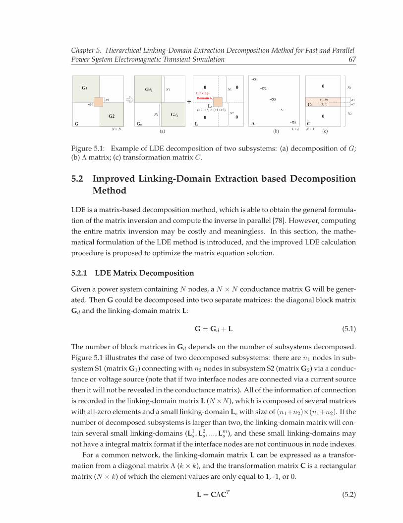
Chapter 5. Hierarchical Linking-Domain Extraction Decomposition Method for Fast and ParallelPower System Electromagnetic Transient Simulation 67
G(a)
+
G1
G2Gd
Linking-Domain
L
Ls
0 0
0 0
N × N
(n1+n2) × (n1+n2)
N1
N2
N1
N2
n1n2
Gd
Gd
2
1
-σ1
...
k × k
-σ2
-σ3
-σkΛ(b)
C
Cs
0
0
N × k
N1
N2
(c)
n1n2
(-1, 0)(1, 0)
Figure 5.1: Example of LDE decomposition of two subsystems: (a) decomposition of G;(b) Λ matrix; (c) transformation matrix C.
5.2 Improved Linking-Domain Extraction based DecompositionMethod
LDE is a matrix-based decomposition method, which is able to obtain the general formula-tion of the matrix inversion and compute the inverse in parallel [78]. However, computingthe entire matrix inversion may be costly and meaningless. In this section, the mathe-matical formulation of the LDE method is introduced, and the improved LDE calculationprocedure is proposed to optimize the matrix equation solution.
5.2.1 LDE Matrix Decomposition
Given a power system containing N nodes, a N ×N conductance matrix G will be gener-ated. Then G could be decomposed into two separate matrices: the diagonal block matrixGd and the linking-domain matrix L:
G = Gd + L (5.1)
The number of block matrices in Gd depends on the number of subsystems decomposed.Figure 5.1 illustrates the case of two decomposed subsystems: there are n1 nodes in sub-system S1 (matrix G1) connecting with n2 nodes in subsystem S2 (matrix G2) via a conduc-tance or voltage source (note that if two interface nodes are connected via a current sourcethen it will not be revealed in the conductance matrix). All of the information of connectionis recorded in the linking-domain matrix L (N×N ), which is composed of several matriceswith all-zero elements and a small linking-domain Ls with size of (n1+n2)×(n1+n2). If thenumber of decomposed subsystems is larger than two, the linking-domain matrix will con-tain several small linking-domains (L1
s,L2s, ...,Lm
s ), and these small linking-domains maynot have a integral matrix format if the interface nodes are not continuous in node indexes.
For a common network, the linking-domain matrix L can be expressed as a transfor-mation from a diagonal matrix Λ (k × k), and the transformation matrix C is a rectangularmatrix (N × k) of which the element values are only equal to 1, -1, or 0.
L = CΛCT (5.2)
Chapter 5. Hierarchical Linking-Domain Extraction Decomposition Method for Fast and ParallelPower System Electromagnetic Transient Simulation 68
Note that k is the number of links connecting the decomposed matrices. Take the case oftwo decomposed subsystems as an example, as shown in Fig. 5.1(b)(c), Λ has k negativeelements in diagonal, and C is composed of all-zero matrices and a small transformationmatrix Cs with size of (n1 + n2) × k. Cs can be regarded as two parts: the upper n1 rowsC(1)s and the lower n2 rows C(2)
s ; every column of C(1)s only has one element equal to -1,
and the other elements are equal to 0; while every column of C(2)s only has one element
equal to 1, and the other elements are equal to 0.Then the general formulation of the inverse matrix of G = Gd+L could be found based
on the Woodbury matrix identity [70]:
G−1 = (Gd + L)−1 = G−1d − G−1
d CQCT G−1d (5.3)
where:Q = (Λ−1 + CT G−1
d C)−1 (5.4)
5.2.2 Improved LDE Computation Procedure
Although computing the matrix inversion G−1 directly could accelerate the simulationprocess significantly when the the conductance matrix G does not change over the sim-ulation duration, the storage and I/O cost increase dramatically when the power systemscale expands. Therefore, in this chapter, the LDE computation procedure is improvedaccordingly.
The improved computational procedure is used to solve the matrix equations withoutstoring the inverted conductance matrix. The goal is to solve for the node voltages v:
Gv = ieq (5.5)
Applying the LDE matrix inversion:
v = G−1ieq = [G−1d − G−1
d CQCT G−1d ]ieq
= G−1d ieq − G−1
d CQCT G−1d ieq
= vDBM − G−1d C(Λ−1 + CT G−1
d C)−1CT vDBM
(5.6)
where vDBM = G−1d ieq is the solution of each decomposed subsystems. The matrix in-
version process of (Λ−1 + CT G−1d C) can also be avoided to reduce the computational and
storage cost:
v = vDBM − G−1d C(Λ−1 + CT G−1
d C)−1CT vDBM
= vDBM − G−1d CvLDM
(5.7)
where vLDM is the solution of the matrix equation below:
(Λ−1 + CT G−1d C)vLDM = CT vDBM (5.8)
Chapter 5. Hierarchical Linking-Domain Extraction Decomposition Method for Fast and ParallelPower System Electromagnetic Transient Simulation 69
As stated in the matrix inversion procedure, C and CT matrix have very special features,which make the computation of G−1
d C and CT vDBM simple without multiplication oper-ations. Therefore, the improved LDE solver computation procedure can be executed asfollows:
1. compute G−1d and vDBM = G−1
d ieq;
2. compute T = G−1d C;
3. compute Λ−1 + CT T and solve vLDM ;
4. compute the final solution v = vDBM − TvLDM ;
Using the above improved LDE computation procedure, the storage cost can be dra-matically reduced. For a N × N conductance matrix that is decomposed into m sub-matrices with equal sizes, the storage cost of the improved LDE method is O[m(N/m)2 +
k2] = O(N2/m+ k2), which is reduced nearly m times over the original LDE method. Al-though the storage is still large compared to the sparse LU factorization based solvers, thebenefits of the fast solution process can be reflected within a certain power system scale.
5.3 Hierarchical LDE Method
From the above procedure it can be observed that the computation of G−1d cannot be
avoided although the computation of G−1 is eliminated. Since only the diagonal blockmatrices in G−1
d are non-zeros, the storage cost can be reduced significantly. However,for large-scale power systems, the conductance matrix could not be decomposed in a fine-grained fashion because such decomposition will result in a large Λ matrix that is not ben-eficial to the overall performance. Therefore, the LDE decomposition will generate largeblock matrices in Gd even after decomposition, which makes the computation of G−1
d alsocostly.
Fortunately, the LDE method is essentially a matrix inversion method, which is able toaccelerate the matrix inversion process of the block matrices in Gd. This means, althoughthe LDE matrix inversion is not used in the improved computation procedure, it can alsobe used to compute G−1
d , and this application of LDE method is just to decompose the sub-systems into further sub-subsystems. Based on this, the multi-level LDE decomposition isproposed, which is called “hierarchical LDE (H-LDE) method”.
5.3.1 Multi-Level LDE Decomposition
When the decomposed subsystems also have relatively large scales, computing the inver-sion of block matrices in Gd still requires a lot of compute effort. In the H-LDE decom-position, the computation of G−1
d could be executed based on the second or even higher
Chapter 5. Hierarchical Linking-Domain Extraction Decomposition Method for Fast and ParallelPower System Electromagnetic Transient Simulation 70
level LDE decomposition to reduce the computational latency. Thus the application ofLDE method could be extended to simulate power systems in a hierarchical manner:
1. decompose the whole system into subsystems for the first-level LDE decomposition,and solve the unknown state-variables using the improved LDE computation proce-dure;
2. if the sizes of decomposed subsystems are still large, decompose the subsystems intosmall sub-subsystems for the second-level LDE decomposition; else, calculate theinversion of the decomposed block matrices directly;
3. if the second-level decomposition still has room for deeper decomposition, then thethird or even higher level decompositions could be exploited to increase the paral-lelism and accelerate the overall execution.
The improved LDE computation procedure is applied for the first level LDE decom-position to reduce the storage and computation cost, because there is no need to computethe inversion of the whole matrix; however, the second or higher level LDE decompositionshould be computed using the original LDE matrix inversion procedure, because the goalof multi-level LDE decomposition is to obtain G−1
d quickly, which could not be avoided.
5.3.2 Computational Complexity Analysis of Hierarchical LDE
Assume the complexity of inverting a N ×N matrix is O(N3) based on the Gauss-Jordanmethod. Then the original LDE method has a complexity of O[N3
j + k3], where Nj is themaximum size of the decomposed block matrices, and k is the number of links connect-ing these decomposed subsystems (SSs). However, this is not applicable for the H-LDEmethod, because complexity of computing G−1
d should be re-evaluated. Assume that thereare r levels of LDE decomposition in total, and the decomposed subsystems nearly havethe same size while the number of links between the decomposed sub-subsystems are alsothe same for the decomposition of different subsystems. This assumption may be not rig-orous, but considering that the power system topology is not dense and the connectionsare relatively distributed on average, this assumption is just an approximation and makessense in the complexity analysis. As shown in Fig. 5.2, after the ith-level decomposition,there are m(i) subsystems decomposed from each subsystem located on the upper level inFig. 5.2, and each decomposed subsystem contains N(i) nodes with total k(i) links connect-ing these subsystems. The relationship between N(i) and m(i) are:
N(i−1) = m(i)N(i) (5.9)
N = m(1)N(1) = ... = (
i∏1
m(i))N(i) (5.10)
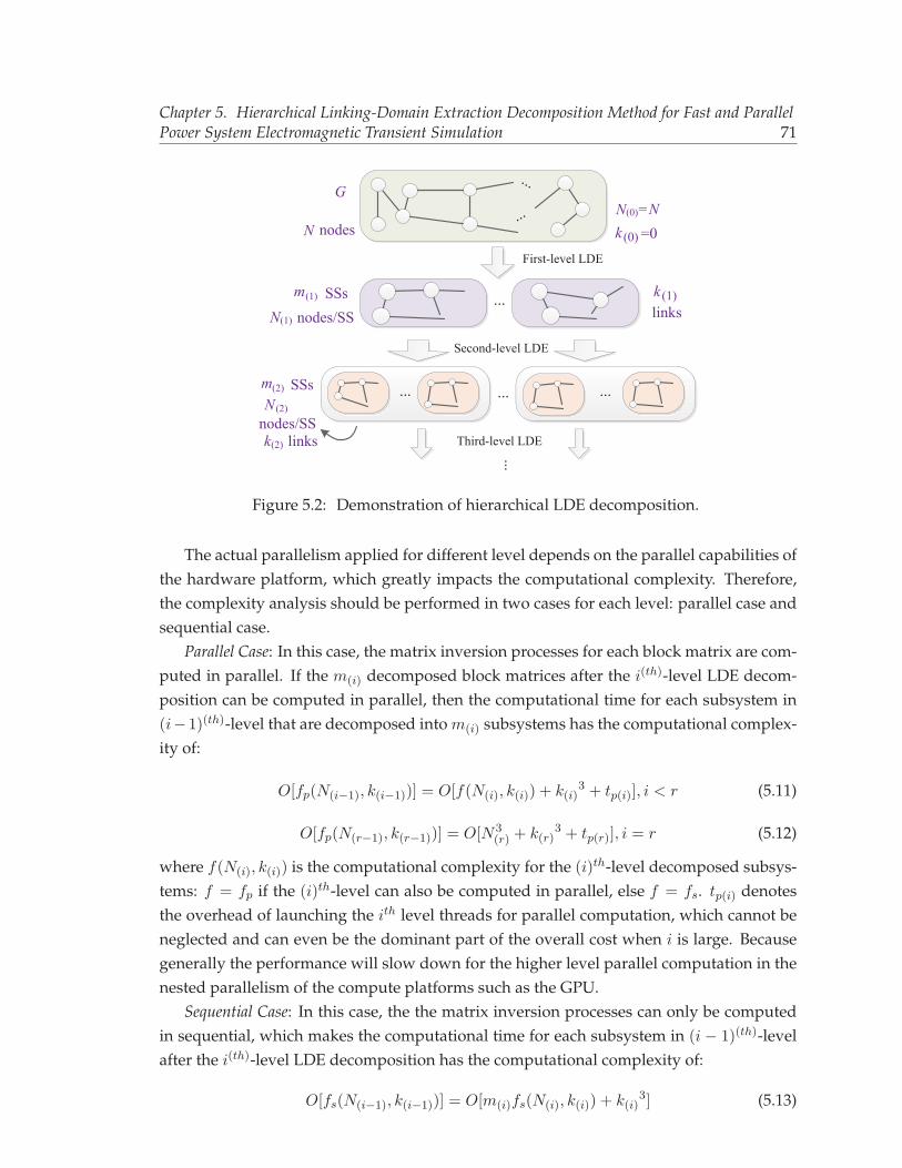
Chapter 5. Hierarchical Linking-Domain Extraction Decomposition Method for Fast and ParallelPower System Electromagnetic Transient Simulation 71
...
First-level LDE
...
......
...
...
G
m
N nodes
SSsN(1) links
k (1)
...... ...
Second-level LDE
Third-level LDE
(1)
nodes/SS
m SSsN (2)
(2)
nodes/SSlinksk(2)
k (0) =0N(0)=N
Figure 5.2: Demonstration of hierarchical LDE decomposition.
The actual parallelism applied for different level depends on the parallel capabilities ofthe hardware platform, which greatly impacts the computational complexity. Therefore,the complexity analysis should be performed in two cases for each level: parallel case andsequential case.
Parallel Case: In this case, the matrix inversion processes for each block matrix are com-puted in parallel. If the m(i) decomposed block matrices after the i(th)-level LDE decom-position can be computed in parallel, then the computational time for each subsystem in(i− 1)(th)-level that are decomposed into m(i) subsystems has the computational complex-ity of:
O[fp(N(i−1), k(i−1))] = O[f(N(i), k(i)) + k(i)3 + tp(i)], i < r (5.11)
O[fp(N(r−1), k(r−1))] = O[N3(r) + k(r)
3 + tp(r)], i = r (5.12)
where f(N(i), k(i)) is the computational complexity for the (i)th-level decomposed subsys-tems: f = fp if the (i)th-level can also be computed in parallel, else f = fs. tp(i) denotesthe overhead of launching the ith level threads for parallel computation, which cannot beneglected and can even be the dominant part of the overall cost when i is large. Becausegenerally the performance will slow down for the higher level parallel computation in thenested parallelism of the compute platforms such as the GPU.
Sequential Case: In this case, the the matrix inversion processes can only be computedin sequential, which makes the computational time for each subsystem in (i − 1)(th)-levelafter the i(th)-level LDE decomposition has the computational complexity of:
O[fs(N(i−1), k(i−1))] = O[m(i)fs(N(i), k(i)) + k(i)3] (5.13)
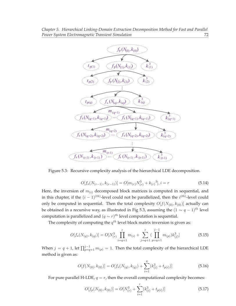
Chapter 5. Hierarchical Linking-Domain Extraction Decomposition Method for Fast and ParallelPower System Electromagnetic Transient Simulation 72
f (N ,k )p (0) (0)
f (N ,k )p (1) (1) k (1)3
m (q+1)
f (N ,k )p (2) (2) k (2)3
...
k (q)3
f (N ,k )s (q+1) (q+1) k(q+1)3
f (N ,k )s (q) (q)
...
k(q+2)3...
m(q+2)
...
k (r-1)3...
m (r-1)
f (N ,k )s (q+1) (q+1)
f (N ,k )s (q+2) (q+2) f (N ,k )s (q+2) (q+2)
f (N ,k )s (r-1) (r-1) f (N ,k )s (r-1) (r-1)
t p(1)
tp(2)
tp(q)
Figure 5.3: Recursive complexity analysis of the hierarchical LDE decomposition.
O[fs(N(r−1), k(r−1))] = O[m(r)N3(r) + k(r)
3], i = r (5.14)
Here, the inversion of m(i) decomposed block matrices is computed in sequential, andin this chapter, if the (i − 1)(th)-level could not be parallelized, then the i(th)-level couldonly be computed in sequential. Then the total complexity O[f(N(0), k(0))] actually canbe obtained in a recursive way, as illustrated in Fig 5.3, assuming the (1 ∼ q − 1)th levelcomputation is parallelized and (q ∼ r)th level computation is sequential.
The complexity of computing the qth level block matrix inversion is given as:
O[fs(N(q), k(q))] = O[N3(r)
r∏i=q+1
m(i) +
r∑j=q+1
(
j−1∏p=q+1
m(p))k3(j)] (5.15)
When j = q + 1, let∏j−1
p=q+1m(p) = 1. Then the total complexity of the hierarchical LDEmethod is given as:
O[f(N(0), k(0))] = O[fs(N(q), k(q)) +
q∑i=1
(k3(i) + tp(i))] (5.16)
For pure parallel H-LDE, q = r, then the overall computational complexity becomes:
O[fp(N(0), k(0))] = O[N3(r) +
r∑i=1
(k3(i) + tp(i))] (5.17)
Chapter 5. Hierarchical Linking-Domain Extraction Decomposition Method for Fast and ParallelPower System Electromagnetic Transient Simulation 73
For pure sequential H-LDE, q = 0, then the overall computational complexity becomes:
O[fs(N(0), k(0))] = O[N3(r)
r∏i=1
m(i) +
r∑j=1
(
j−1∏p=1
m(p))k3(j)] (5.18)
where∏0
p=1m(p) = 1. Note that (5.16)-(5.18) are only the approximation and ideal re-sults of complexity analysis, but they can still be used to guide the specific decompositionconfiguration given a power system case at hand.
5.3.3 Specific Decomposition Principles
Based on the complexity analysis, the number of decomposition levels and the numberof decomposed subsystems in each level can be evaluated given a specific power systemtopology and parallel platform. Generally, two decomposition principles are proposed toimprove the decomposition performance.
Principle 1: In the (i = 1 ∼ r − 1)th level, make the number of connecting links k(i) tobe smaller than the size of the decomposed subsystems N(i); and in the rth level, make abalance between k(r) and N(r).
This principle is inspired by (5.11)-(5.14), as can be seen that if k(i) > N(i) in the (i =
1 ∼ r− 1)th level, then O[k3(i)] will be the dominant part of the complexity no matter in theparallel case or sequential case, which means, there is no need to perform a higher leveldecomposition. And in the rth level, the balance should be made between k(r) and N(r)
because it is the last level and should make sure that O[f(N(r−1), k(r−1))] is minimized, justlike the one-level traditional LDE method.
Principle 2: The launching of a higher level should achieve a lower computation timebut not result in a larger latency, that is, for parallel computing:
O[f(N(i), k(i)) + k(i)3 + tp(i)] < O[N3
(i−1)] (5.19)
where tp(i) contains the overhead of launching child kernels for parallel computation aswell as the latency of synchronization between the kernels. And for sequential computing:
O[m(i)fs(N(i), k(i)) + k(i)3] < O[N3
(i−1)] (5.20)
This principle is used to judge whether a deeper decomposition is required, becausethe common parallel platforms such as GPU have limited capabilities of parallelism andthe overhead of launching child kernels is significant. For sequential computation, thedecomposition should also make sure the sum of latencies for each subsystem computationis smaller than the latency without decomposition. For example, when decomposing a60×60 block matrix into three 20×20 block matrices for sequential computing, it shouldbe guaranteed that 3 × t20 + tk20 < t60, where t20 denotes the latency of computing theinversion of a 20×20 block matrix, and tk20 denotes the latency of computing the Q matrix
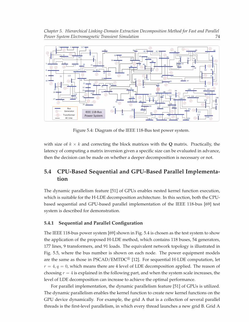
Chapter 5. Hierarchical Linking-Domain Extraction Decomposition Method for Fast and ParallelPower System Electromagnetic Transient Simulation 74
3 1 2 117
12
14 33
35
36
13
1576
4
5
11
8
9
16
17 18
19
1020
34
30
31 113
21
2229
28
27
2324
25
26
115
114
32 7271
70
74
73
75
37
4338
69
39 40 41
4445 42
4648
49
47
5150
52
53
54
58 57
56 55
59
60
61
63
66
65 67
62
64
116
6881
7780 99
106 107
104
105
1009897
9694
95 93
9289
90 91
87
86
85
118
76 82
8384
88
101
102 110
108
109
103
111112
78 79
IEEE 118-BusPower System
AC Line
Generator
Transformer
Bus
Figure 5.4: Diagram of the IEEE 118-Bus test power system.
with size of k × k and correcting the block matrices with the Q matrix. Practically, thelatency of computing a matrix inversion given a specific size can be evaluated in advance,then the decision can be made on whether a deeper decomposition is necessary or not.
5.4 CPU-Based Sequential and GPU-Based Parallel Implementa-tion
The dynamic parallelism feature [51] of GPUs enables nested kernel function execution,which is suitable for the H-LDE decomposition architecture. In this section, both the CPU-based sequential and GPU-based parallel implementation of the IEEE 118-bus [69] testsystem is described for demonstration.
5.4.1 Sequential and Parallel Configuration
The IEEE 118-bus power system [69] shown in Fig. 5.4 is chosen as the test system to showthe application of the proposed H-LDE method, which contains 118 buses, 54 generators,177 lines, 9 transformers, and 91 loads. The equivalent network topology is illustrated inFig. 5.5, where the bus number is shown on each node. The power equipment modelsare the same as those in PSCAD/EMTDC� [12]. For sequential H-LDE computation, letr = 4, q = 0, which means there are 4 level of LDE decomposition applied. The reason ofchoosing r = 4 is explained in the following part, and when the system scale increases, thelevel of LDE decomposition can increase to achieve the optimal performance.
For parallel implementation, the dynamic parallelism feature [51] of GPUs is utilized.The dynamic parallelism enables the kernel function to create new kernel functions on theGPU device dynamically. For example, the grid A that is a collection of several parallelthreads is the first-level parallelism, in which every thread launches a new grid B. Grid A
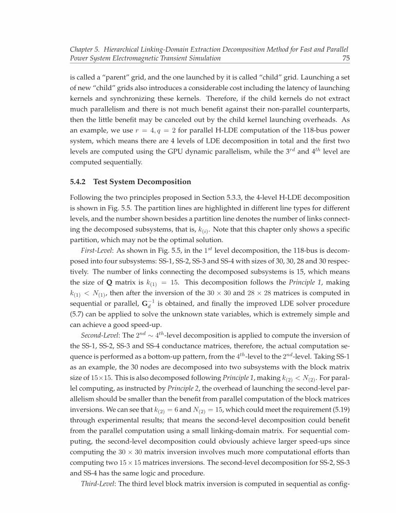
Chapter 5. Hierarchical Linking-Domain Extraction Decomposition Method for Fast and ParallelPower System Electromagnetic Transient Simulation 75
is called a “parent” grid, and the one launched by it is called “child” grid. Launching a setof new “child” grids also introduces a considerable cost including the latency of launchingkernels and synchronizing these kernels. Therefore, if the child kernels do not extractmuch parallelism and there is not much benefit against their non-parallel counterparts,then the little benefit may be canceled out by the child kernel launching overheads. Asan example, we use r = 4, q = 2 for parallel H-LDE computation of the 118-bus powersystem, which means there are 4 levels of LDE decomposition in total and the first twolevels are computed using the GPU dynamic parallelism, while the 3rd and 4th level arecomputed sequentially.
5.4.2 Test System Decomposition
Following the two principles proposed in Section 5.3.3, the 4-level H-LDE decompositionis shown in Fig. 5.5. The partition lines are highlighted in different line types for differentlevels, and the number shown besides a partition line denotes the number of links connect-ing the decomposed subsystems, that is, k(i). Note that this chapter only shows a specificpartition, which may not be the optimal solution.
First-Level: As shown in Fig. 5.5, in the 1st level decomposition, the 118-bus is decom-posed into four subsystems: SS-1, SS-2, SS-3 and SS-4 with sizes of 30, 30, 28 and 30 respec-tively. The number of links connecting the decomposed subsystems is 15, which meansthe size of Q matrix is k(1) = 15. This decomposition follows the Principle 1, makingk(1) < N(1), then after the inversion of the 30 × 30 and 28 × 28 matrices is computed insequential or parallel, G−1
d is obtained, and finally the improved LDE solver procedure(5.7) can be applied to solve the unknown state variables, which is extremely simple andcan achieve a good speed-up.
Second-Level: The 2nd ∼ 4th-level decomposition is applied to compute the inversion ofthe SS-1, SS-2, SS-3 and SS-4 conductance matrices, therefore, the actual computation se-quence is performed as a bottom-up pattern, from the 4th-level to the 2nd-level. Taking SS-1as an example, the 30 nodes are decomposed into two subsystems with the block matrixsize of 15×15. This is also decomposed following Principle 1, making k(2) < N(2). For paral-lel computing, as instructed by Principle 2, the overhead of launching the second-level par-allelism should be smaller than the benefit from parallel computation of the block matricesinversions. We can see that k(2) = 6 and N(2) = 15, which could meet the requirement (5.19)through experimental results; that means the second-level decomposition could benefitfrom the parallel computation using a small linking-domain matrix. For sequential com-puting, the second-level decomposition could obviously achieve larger speed-ups sincecomputing the 30 × 30 matrix inversion involves much more computational efforts thancomputing two 15×15 matrices inversions. The second-level decomposition for SS-2, SS-3and SS-4 has the same logic and procedure.
Third-Level: The third level block matrix inversion is computed in sequential as config-
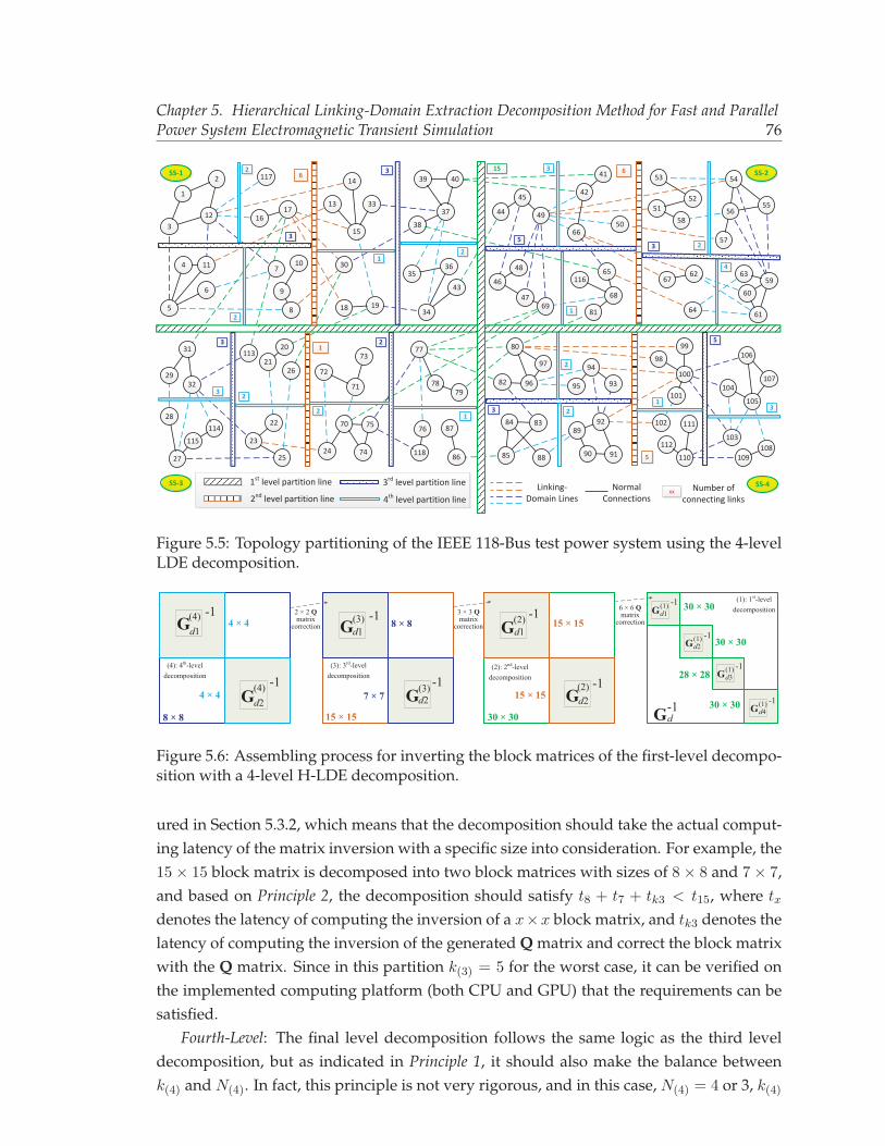
Chapter 5. Hierarchical Linking-Domain Extraction Decomposition Method for Fast and ParallelPower System Electromagnetic Transient Simulation 76
1
2 117
9
10
76
36
312
14
13
15
1918
1716
85
7
6
114
32
11331
29
28114
115
27 25
23
21
22
20
30
26
71
73
72
70
24
66
65
68
116
81
6762
60
6164
5655
5963
57
5851
52
53 54
49
42
50
41
45
48
46
4769
38
43
44
34
37
39 40
33
35
100
101
9998
102
106
107
105
108
104
109
103
110
111
112
93
94
95
92
91
97
80
7996
89
88
838487
86 8574
75
118
77
78 82
90
15 66
5
1
1st level partition line
2nd level partition line
3rd level partition line
4th level partition lineLinking-
Domain LinesNormal
Connectionsxx Number of
connecting links
2SS-1 SS-2
SS-4SS-3
3
2
3
23
3
12
2
12
5
3
1
3 2
4
3 2
2
5
13
Figure 5.5: Topology partitioning of the IEEE 118-Bus test power system using the 4-levelLDE decomposition.
30 × 30
30 × 30
28 × 28
30 × 3015 × 15
30 × 3015 × 15
6 × 6 Qmatrix
correction
(1): 1st-leveldecomposition
G-1
d1(2)
G-1
d2(2)
(2): 2nd-leveldecomposition
3 × 3 Qmatrix
correction
15 × 15
7 × 7
8 × 8G-1
d1(3)
G-1
d2(3)
(3): 3rd-leveldecomposition
2 × 2 Qmatrix
correction
8 × 8
4 × 4
4 × 4G-1
d1(4)
G-1
d2(4)
(4): 4th-leveldecomposition
G-1d
G-1
d1(1)
G-1
d2(1)
G-1
d3(1)
G-1
d4(1)
Figure 5.6: Assembling process for inverting the block matrices of the first-level decompo-sition with a 4-level H-LDE decomposition.
ured in Section 5.3.2, which means that the decomposition should take the actual comput-ing latency of the matrix inversion with a specific size into consideration. For example, the15× 15 block matrix is decomposed into two block matrices with sizes of 8× 8 and 7× 7,and based on Principle 2, the decomposition should satisfy t8 + t7 + tk3 < t15, where tx
denotes the latency of computing the inversion of a x×x block matrix, and tk3 denotes thelatency of computing the inversion of the generated Q matrix and correct the block matrixwith the Q matrix. Since in this partition k(3) = 5 for the worst case, it can be verified onthe implemented computing platform (both CPU and GPU) that the requirements can besatisfied.
Fourth-Level: The final level decomposition follows the same logic as the third leveldecomposition, but as indicated in Principle 1, it should also make the balance betweenk(4) and N(4). In fact, this principle is not very rigorous, and in this case, N(4) = 4 or 3, k(4)
Chapter 5. Hierarchical Linking-Domain Extraction Decomposition Method for Fast and ParallelPower System Electromagnetic Transient Simulation 77
is also equal to or smaller than 3.Fifth or Higher Level: From Fig. 5.5 it can be seen that for N(4) = 4 or 3, making a
higher level LDE decomposition is not necessary. Because computing the inverse of a 4×4
matrix does not involve much overhead, and if it is decomposed into smaller matrices,computing smaller matrix inversions and correcting them with the Q matrix will introduceextra latencies, which are larger than the benefit of decomposition and simply violate thePrinciple 2.
From the above multi-level decomposition configurations, it can be observed that themaximum matrix that is actually required to be inverted is 4×4 for block matrices and 6×6
for Q matrices (k(2) = 6). The 15 × 15 Q matrix (k(1) = 15) is not required to be inverteddue to the proposed improved LDE computation procedure (5.7); the 30 × 30 and 28 × 28
block matrices inversions are actually assembled using the inverted 4 × 4 and 3 × 3 blockmatrices of the 4th-level decomposition, as shown in Fig. 5.6. Therefore, the computationaleffort of H-LDE is greatly reduced compared to the original LDE method that computesthe 30× 30 and 28× 28 block matrices inversions directly.
5.5 Simulation Results and Verification
In this section, the matrix equations of the IEEE 39, 57, 118, and 300 bus benchmark testpower systems [83] and the auto-generated 400/500/600-bus power systems are solvedusing the H-LDE method, and the speed-ups are evaluated on both the Intel� i5-7300HQ2.GHZ CPU with 8G RAM and the NVIDIA� Tesla V100 GPU platform with 5012 cores[82] by comparing with the Gauss-Jordan method, original LDE method, LU factorizationwith Gauss’s algorithm [5] and KLU sparse matrix equation solution [79] method.
5.5.1 Speed-Up of GPU-Based Parallel H-LDE Computation
The performance evaluation of GPU-based parallel H-LDE computation is separated fromthe CPU-based sequential computation, because they have different orders of magnitudein latencies and different application contexts. In this case, the conductance is regarded aschangeable during simulation, therefore, the Gauss-Jordan (GJ) method is chosen as thebase, since the pure LU factorization without re-ordering has a slightly larger complexityfor a changeable conductance matrix and could not expose much parallelism possibilitiescompared to the GJ method. The matrix equation solver latency of the proposed H-LDEmethod is compared with the traditional Gauss-Jordan (GJ), Schur Complement (SC) andoriginal LDE (O-LDE) method. In this chapter, 2-level dynamic parallelism is exploited:the computation procedure of the GJ method could be not expose much parallelism, al-though some rows and columns of the pivoting or reduction operations can be computedin parallel; the matrix inversion of the block matrices generated by the SC and O-LDEmethod could be computed in parallel for the first level parallelism, but the application
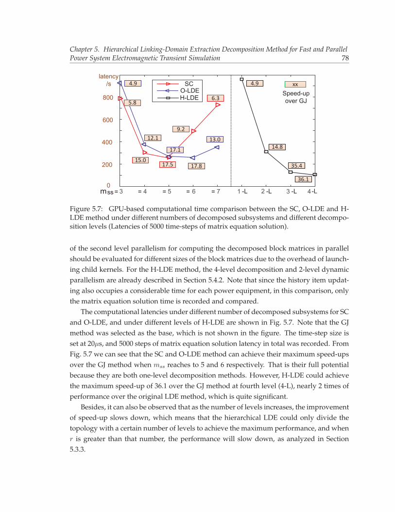
Chapter 5. Hierarchical Linking-Domain Extraction Decomposition Method for Fast and ParallelPower System Electromagnetic Transient Simulation 78
3 4 5 6 7 1 2 3 40
200
400
600
800
SCO-LDEH-LDE
xxSpeed-upover GJ
latency/s
ss= = = = = -L -L -L -L
5.8
m
15.017.5
9.2
6.3
4.9
12.1
17.1
17.8
13.0
4.9
14.8
35.4
36.1
Figure 5.7: GPU-based computational time comparison between the SC, O-LDE and H-LDE method under different numbers of decomposed subsystems and different decompo-sition levels (Latencies of 5000 time-steps of matrix equation solution).
of the second level parallelism for computing the decomposed block matrices in parallelshould be evaluated for different sizes of the block matrices due to the overhead of launch-ing child kernels. For the H-LDE method, the 4-level decomposition and 2-level dynamicparallelism are already described in Section 5.4.2. Note that since the history item updat-ing also occupies a considerable time for each power equipment, in this comparison, onlythe matrix equation solution time is recorded and compared.
The computational latencies under different number of decomposed subsystems for SCand O-LDE, and under different levels of H-LDE are shown in Fig. 5.7. Note that the GJmethod was selected as the base, which is not shown in the figure. The time-step size isset at 20μs, and 5000 steps of matrix equation solution latency in total was recorded. FromFig. 5.7 we can see that the SC and O-LDE method can achieve their maximum speed-upsover the GJ method when mss reaches to 5 and 6 respectively. That is their full potentialbecause they are both one-level decomposition methods. However, H-LDE could achievethe maximum speed-up of 36.1 over the GJ method at fourth level (4-L), nearly 2 times ofperformance over the original LDE method, which is quite significant.
Besides, it can also be observed that as the number of levels increases, the improvementof speed-up slows down, which means that the hierarchical LDE could only divide thetopology with a certain number of levels to achieve the maximum performance, and whenr is greater than that number, the performance will slow down, as analyzed in Section5.3.3.
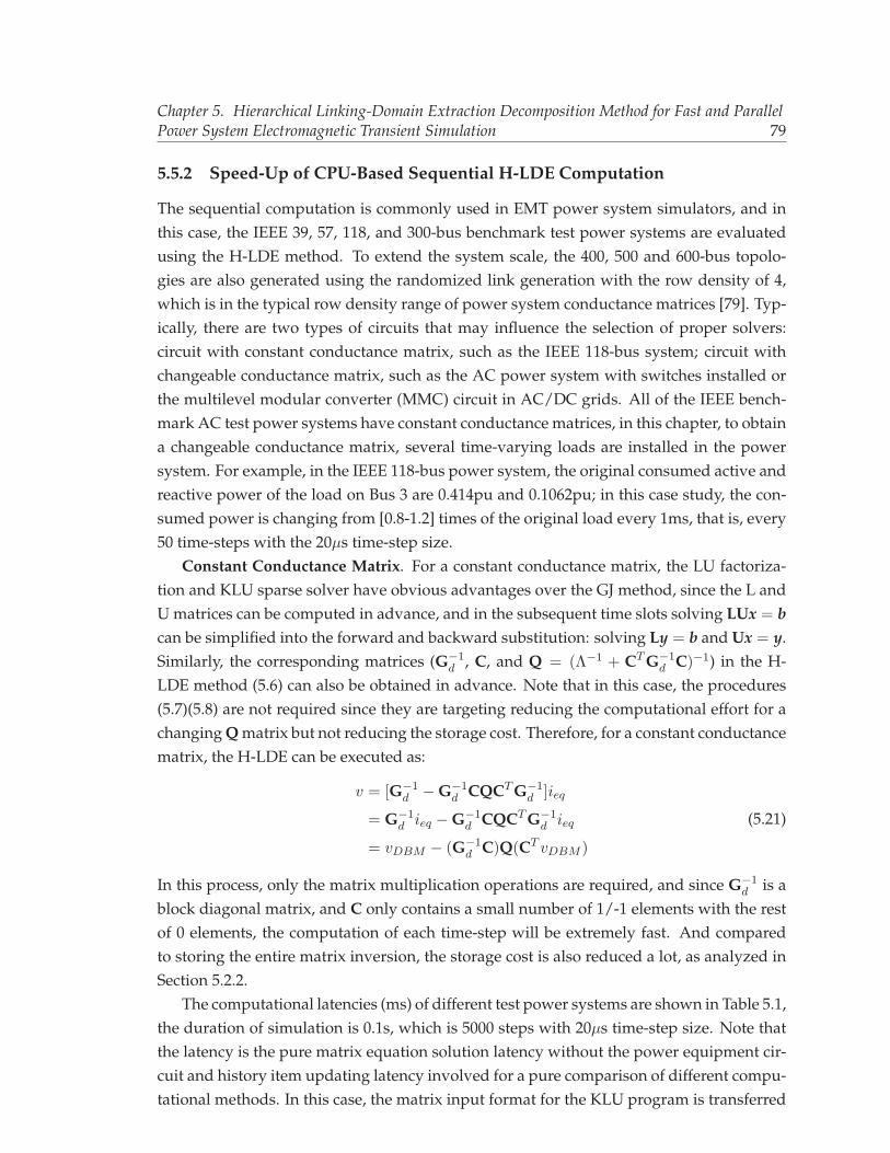
Chapter 5. Hierarchical Linking-Domain Extraction Decomposition Method for Fast and ParallelPower System Electromagnetic Transient Simulation 79
5.5.2 Speed-Up of CPU-Based Sequential H-LDE Computation
The sequential computation is commonly used in EMT power system simulators, and inthis case, the IEEE 39, 57, 118, and 300-bus benchmark test power systems are evaluatedusing the H-LDE method. To extend the system scale, the 400, 500 and 600-bus topolo-gies are also generated using the randomized link generation with the row density of 4,which is in the typical row density range of power system conductance matrices [79]. Typ-ically, there are two types of circuits that may influence the selection of proper solvers:circuit with constant conductance matrix, such as the IEEE 118-bus system; circuit withchangeable conductance matrix, such as the AC power system with switches installed orthe multilevel modular converter (MMC) circuit in AC/DC grids. All of the IEEE bench-mark AC test power systems have constant conductance matrices, in this chapter, to obtaina changeable conductance matrix, several time-varying loads are installed in the powersystem. For example, in the IEEE 118-bus power system, the original consumed active andreactive power of the load on Bus 3 are 0.414pu and 0.1062pu; in this case study, the con-sumed power is changing from [0.8-1.2] times of the original load every 1ms, that is, every50 time-steps with the 20μs time-step size.
Constant Conductance Matrix. For a constant conductance matrix, the LU factoriza-tion and KLU sparse solver have obvious advantages over the GJ method, since the L andU matrices can be computed in advance, and in the subsequent time slots solving LUx = bcan be simplified into the forward and backward substitution: solving Ly = b and Ux = y.Similarly, the corresponding matrices (G−1
d , C, and Q = (Λ−1 + CT G−1d C)−1) in the H-
LDE method (5.6) can also be obtained in advance. Note that in this case, the procedures(5.7)(5.8) are not required since they are targeting reducing the computational effort for achanging Q matrix but not reducing the storage cost. Therefore, for a constant conductancematrix, the H-LDE can be executed as:
v = [G−1d − G−1
d CQCT G−1d ]ieq
= G−1d ieq − G−1
d CQCT G−1d ieq
= vDBM − (G−1d C)Q(CT vDBM )
(5.21)
In this process, only the matrix multiplication operations are required, and since G−1d is a
block diagonal matrix, and C only contains a small number of 1/-1 elements with the restof 0 elements, the computation of each time-step will be extremely fast. And comparedto storing the entire matrix inversion, the storage cost is also reduced a lot, as analyzed inSection 5.2.2.
The computational latencies (ms) of different test power systems are shown in Table 5.1,the duration of simulation is 0.1s, which is 5000 steps with 20μs time-step size. Note thatthe latency is the pure matrix equation solution latency without the power equipment cir-cuit and history item updating latency involved for a pure comparison of different compu-tational methods. In this case, the matrix input format for the KLU program is transferred
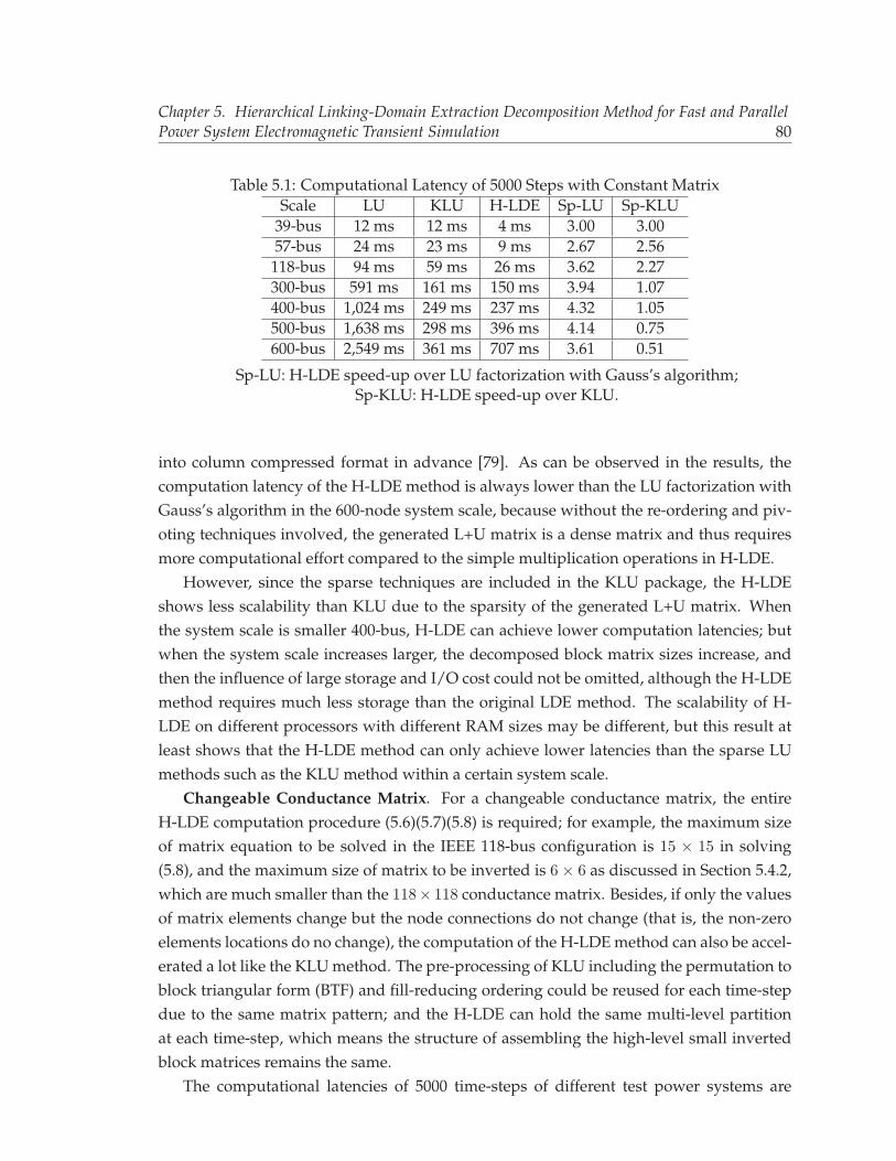
Chapter 5. Hierarchical Linking-Domain Extraction Decomposition Method for Fast and ParallelPower System Electromagnetic Transient Simulation 80
Table 5.1: Computational Latency of 5000 Steps with Constant MatrixScale LU KLU H-LDE Sp-LU Sp-KLU
39-bus 12 ms 12 ms 4 ms 3.00 3.0057-bus 24 ms 23 ms 9 ms 2.67 2.56
118-bus 94 ms 59 ms 26 ms 3.62 2.27300-bus 591 ms 161 ms 150 ms 3.94 1.07400-bus 1,024 ms 249 ms 237 ms 4.32 1.05500-bus 1,638 ms 298 ms 396 ms 4.14 0.75600-bus 2,549 ms 361 ms 707 ms 3.61 0.51
Sp-LU: H-LDE speed-up over LU factorization with Gauss’s algorithm;Sp-KLU: H-LDE speed-up over KLU.
into column compressed format in advance [79]. As can be observed in the results, thecomputation latency of the H-LDE method is always lower than the LU factorization withGauss’s algorithm in the 600-node system scale, because without the re-ordering and piv-oting techniques involved, the generated L+U matrix is a dense matrix and thus requiresmore computational effort compared to the simple multiplication operations in H-LDE.
However, since the sparse techniques are included in the KLU package, the H-LDEshows less scalability than KLU due to the sparsity of the generated L+U matrix. Whenthe system scale is smaller 400-bus, H-LDE can achieve lower computation latencies; butwhen the system scale increases larger, the decomposed block matrix sizes increase, andthen the influence of large storage and I/O cost could not be omitted, although the H-LDEmethod requires much less storage than the original LDE method. The scalability of H-LDE on different processors with different RAM sizes may be different, but this result atleast shows that the H-LDE method can only achieve lower latencies than the sparse LUmethods such as the KLU method within a certain system scale.
Changeable Conductance Matrix. For a changeable conductance matrix, the entireH-LDE computation procedure (5.6)(5.7)(5.8) is required; for example, the maximum sizeof matrix equation to be solved in the IEEE 118-bus configuration is 15 × 15 in solving(5.8), and the maximum size of matrix to be inverted is 6× 6 as discussed in Section 5.4.2,which are much smaller than the 118× 118 conductance matrix. Besides, if only the valuesof matrix elements change but the node connections do not change (that is, the non-zeroelements locations do no change), the computation of the H-LDE method can also be accel-erated a lot like the KLU method. The pre-processing of KLU including the permutation toblock triangular form (BTF) and fill-reducing ordering could be reused for each time-stepdue to the same matrix pattern; and the H-LDE can hold the same multi-level partitionat each time-step, which means the structure of assembling the high-level small invertedblock matrices remains the same.
The computational latencies of 5000 time-steps of different test power systems are
Chapter 5. Hierarchical Linking-Domain Extraction Decomposition Method for Fast and ParallelPower System Electromagnetic Transient Simulation 81
Table 5.2: Computational Latency (ms) of 5000 Steps with Changeable MatrixScale LU KLU H-LDE Sp-LU Sp-KLU
39-bus 74 ms 138 ms 31 ms 2.39 4.4557-bus 196 ms 339 ms 90 ms 2.18 3.77118-bus 1,379 ms 953 ms 331 ms 4.17 2.88300-bus 19,808 ms 2,536 ms 1,371 ms 14.45 1.85400-bus 37,814 ms 3,493 ms 2,476 ms 15.27 1.41500-bus 89,133 ms 4,538 ms 5,702 ms 15.63 0.80600-bus 218,758 ms 5,101 ms 13,115 ms 16.68 0.39
shown in Table 5.2, the H-LDE speed-up over the LU factorization without sparse tech-niques involved is increasing as the system scale increases, which shows that the H-LDEmethod is more scalable than the pure LU factorization. For the KLU, since the pre-processing procedures are involved, it could not obtain good performance in the smallscale system. But as the fill-in reducing algorithms are applied, the generated L+U ma-trix is still a sparse matrix and thus the method can scale very well when the system scaleexpands. For the H-LDE method, the computational procedure for computing the blockmatrices inversions can be significantly accelerated, and thus within the 400-bus systemscale it can even achieve lower latencies than the sparse KLU method. It can be expectedthat if the CPU multi-core parallel architecture is utilized, the block matrices inversions canbe computed in parallel to achieve a faster speed. Therefore, although sparse techniquesare suitable for large-scale circuit simulation, the H-LDE method can also be applied forthe fast and parallel EMT power system simulation within a certain power system scale.
5.6 Summary
In this chapter, the capability of LDE method is fully exploited by the proposed hierar-chical LDE (H-LDE) method. First, the LDE computation procedure is improved to avoidstoring the entire inverted conductance matrix to reduce the storage cost. Based on this,the detailed decomposition configuration for a specific number of decomposition levels ispresented. Then, the complexity of H-LDE decomposition is analyzed, based on which thetwo decomposition principles are proposed to improve the decomposition performance.Based on the proposed decomposition principles, the IEEE 118-bus test power system isdecomposed into four levels to demonstrate the application of the H-LDE method. Thesimulation results and speed-ups over the original LDE method, the classical LU factoriza-tion and the KLU sparse matrix equation solvers show that the proposed H-LDE methodcould achieve a lower latency in the 400-bus level power system. Therefore, the H-LDEmethod can be applied for the fast and parallel power system circuit simulation within acertain power system scale.
6Real-Time Co-Emulation Framework for
EMT-Based Power System andCommunication Network on FPGA-MPSoC
Hardware Architecture
With the expansion of smart grid infrastructure world-wide, modeling the interaction be-tween power systems and communication networks becomes paramount and has createda new challenge of co-simulating the two domains before commissioning. Existing co-simulation methods mostly concentrate on the off-line software-level interface design tosynchronize messages between the simulators of both domains. Instead of simulating insoftware with a large latency, this chapter proposes a novel real-time co-emulation (RTCE)framework on FPGA-MPSoC based hardware architecture for a more practical emulationof real-world cyber-physical systems. The discrete-time based power system electromag-netic transient (EMT) emulation is executed in programmable hardware units so that thetransient-level behaviour can be captured in real-time, while the discrete-event based com-munication network emulation is modeled in abstraction-level or directly executed on thehardware PHY and network ports of the FPGA-MPSoC platform, which can perform thecommunication networking in real-time. The data exchange between two domains is han-dled within each platform with an extremely low latency, which is sufficiently fast forreal-time interaction; and the multi-board scheme is deployed to practically emulate thecommunication between different power system areas. The hardware resource cost andemulation latency for the test system and case studies are evaluated to demonstrate thevalidity and effectiveness of the proposed RTCE framework.
82
Chapter 6. Real-Time Co-Emulation Framework for EMT-Based Power System andCommunication Network on FPGA-MPSoC Hardware Architecture 83
6.1 Introduction
With the innovations in electric power grids and information and communication tech-nologies (ICT), the traditional power systems are evolving into complex cyber-physicalsystems (CPS), which increasingly leverages the capabilities of data communication andcomputation to enhance the flexibility of power transfer [6] in the smart grid (SG). Onemajor concern in smart grid research is to simulate the entire behavior of the system to ad-equately evaluate the influence of the interplay between digital world and physical equip-ment. However, since the power system and communication network have distinctly dif-ferent working principles and simulation tools, simulating the entire behavior of the twodomains (so-called co-simulation) is quite challenging [6, 43].
Various co-simulation frameworks have been proposed in the recent past since the firstinterface for the PSCAD/EMTDC� simulator [36] to integrate an agent-based distributedapplication into the simulation was developed. Most of these works are not to design acomplete simulator that could finish all required functions in one software package butattempt interfacing two existing simulators of each domain, because there are alreadyvarious mature power system and communication network simulators available. Unfor-tunately, there does not exist universally accepted interfaces for data exchange betweensimulators of the two domains due to their different working principles or even oper-ation systems. Thus, the main concern of these co-simulator frameworks [37–42] is toproperly handle data exchange and synchronization for related events in both domains atruntime. Most co-simulators mainly distinguish from each other by the type of power sys-tem/communication network simulators used, the methods applied for synchronization,and the application scenarios. For example, EPOCHS [40] is mainly used for wide areamonitoring, which uses PSCAD/EMTDC� and PSLF� for power system simulation, andNS-2 for communication network simulation; the periodic synchronization mechanism isadopted. GECO [41] interfaces the power system simulator PSLF� and network simulatorNS-2, and the synchronization is based on a global event driven on-demand mechanism.INSPIRE [42] uses dynamic synchronization points for the interfacing of DigSilent� andOPNET simulators. In [84] the Matlab and C++ based platforms are applied for powersystem and cyber system simulation respectively, and the how a cyber-contingency affectspower system operations was investigated. The co-simulation platform presented in [85]was implemented based on OPAL-RT� real-time simulator and Riverbed Modeler to ex-amine the power grid vulnerabilities to cyber-physical attacks.
However, the performance of the software-based simulators is relatively low comparedwith actual power and communication network devices even without taking the data ex-change and synchronization time between two simulators into account. If the electromag-netic transient (EMT) is concerned, the simulation process will be extremely slow due tothe small time-step size and massive synchronization requirements. It is therefore diffi-cult to practically simulate and test the adequacy of manufactured protection and control
Chapter 6. Real-Time Co-Emulation Framework for EMT-Based Power System andCommunication Network on FPGA-MPSoC Hardware Architecture 84
equipment responding to potential damage created by transient events in real-time. Al-though the real-time power system simulation approaches have been extensively studiedin past works, the real-time co-simulation of power system and communication networkhas rarely been investigated. In [86] and [87], the real-time co-simulation frameworks werediscussed. Similar with the other software-based co-simulators, in these two works, theinterface design and synchronization scheme are still the main concerns. To achieve real-time power system simulation, the commercial simulator RT-LAB� was utilized; thus theimplementation details of the entire co-simulator are absent. In [88] and [89], the hybridhardware and software platforms are applied: the communication network simulation ranon the OPNET software simulator on PC computers, while the real-time power systemsimulation was conducted on the RTDS� hardware simulator. The interface design be-tween the two different platforms (dedicated hardware and PC software) is even morecomplicated with loss of generality.
Different from the pure software-based or hybrid hardware and software based co-simulation discussed above, there is no relevant work available for the more practical hard-ware based co-emulation on FPGAs, due to the complexity and specificity of the cyberphysical power system and FPGA/MPSoC platforms. Although the FPGA-MPSoC plat-form that enables flexible programmability and highly paralleled computing environmenthas been used in multi-rate mixed-solver [50], it was purely applied for power systemEMT simulation and no communication networks were involved. If the entire resourcesincluding the fast and parallel computation capabilities of programmable logics and soft-processors, and the physical ethernet network ports could be leveraged for the co-emulationof the power system and communication network, it can be expected that the testing andevaluation process of cyber-physical energy systems would be more practical and be ac-celerated significantly.
Based on the above observations, this work proposes a real-time co-emulation (RTCE)framework executed on hardware FPGA-MPSoC platform instead of interfacing two soft-ware based simulators. To the best of our knowledge, this is the first work that conductsreal-time co-emulation on hybrid FPGA-MPSoC hardware platform. In this work, the en-tire hardware architecture and implementation details for co-emulating the power systemand communication network are given, which utilize all the programmable logics, soft-processor and networking port resources on the FPGA and MPSoC platform, and providea new vision of co-emulation of emerging cyber-physical systems. The advantages andfeatures of the proposed real-time co-emulator are as follows:
1. Power system EMT emulation is carried out on programmable hardware units sothat transients can be captured in real-time;
2. Communication network emulation is modeled in abstraction for transmission-levelnetworking and directly conducted on real-world physical ports to form the function-level networking;
Chapter 6. Real-Time Co-Emulation Framework for EMT-Based Power System andCommunication Network on FPGA-MPSoC Hardware Architecture 85
3. Power system and communication network emulation modules are embedded withineach FPGA/MPSoC board so that the data exchange and synchronization betweenthe two domains are sufficiently fast for real-time interaction;
4. System monitoring and control applications are executed within the soft processorsof FPGA-MPSoC platform so that the system control can be programmed flexiblyto respond to the physical system events such as overcurrents or communicationbreakdown such as link failures.
Based on the above advantages, the proposed RTCE framework can achieve real-timeco-emulation of power system and communication network, which resembles a real-worldcyber-physical system. The IEEE 39-bus system is chosen as the test case emulated on thehybrid FPGA-MPSoC hardware platform, and the real-time emulation results are capturedfor the overcurrent and communication link failure case studies.
6.2 Co-simulation Background
In general, simulation plays an important role in design and test of both power systemand communication networks. Power system simulation is mainly used for system plan-ning and operating, while the network simulation is mainly used for developing and test-ing new architecture or protocols. This section introduces the basic concepts and com-monly used methods in both simulation domains, and then presents the main challengesof power-communication co-simulation.
6.2.1 Power System Simulation
The power system simulation methods can be classified into two categories: steady-statesimulation and continuous-time simulation. Steady-state simulation is mainly used forpower flow calculation, which uses large time steps (typically seconds/minutes) and is notable to capture the transient dynamics. Continuous-time simulation is commonly used tocapture the transient behaviour through continuous time model, which requires solvingthe system equations within a very small time-step (typically at microsecond level). Sincein most cases co-simulation is used to analyze the impact of short-term communicationfailure or the instant response of system control, continuous-time simulation is mainlyapplied for dynamic power system simulation and therefore is the main focus of this work.
In EMT simulation, each power equipment can be modeled into an equivalent circuitusing basic power elements such as the resistor, capacitor and current source. Then thewhole power system can be described using a set of differential equations obtained bygathering all the power equipment models and applying circuit laws, where the state vari-ables of differential equations are to be solved. The numerical integration algorithms suchas Trapezoidal Rule and Backward Euler methods are usually applied to those differential
Chapter 6. Real-Time Co-Emulation Framework for EMT-Based Power System andCommunication Network on FPGA-MPSoC Hardware Architecture 86
equations to solve the state variables within each discrete time-step. Therefore, the EMTpower system simulation is discrete-time based simulation, and a small time-step size (typ-ically at microsecond level) is always required to capture the transient level behaviours.
6.2.2 Communication Network Simulation
Different from power systems, the elements in communication networks are modeled notbased on physical principles but on their functionality, and thus there are no differentialequations or matrix equations to be solved. Instead, the components in communicationnetworks simply receive, modify and send data packets, and thus the process of each net-work element is always modeled into a sequence of discrete events that occur unevenlyin time, where each event represents an operation of packet processing or transmission.In this context, the communication network simulator refers to a program running onsoftware or hardware to simulate the behaviour of a user-defined network topology, andeach node in the simulator executes the packet processing procedure similar to real-worldequipment.
The basic network component in the cyber-physical power system is the sampling andreporting device, or a smart meter, which is responsible to measure the electrical values ofthe power system and report the measurements to the system controller. The phasor mea-surement unit (PMU) [90] is a commonly used basic network component that is deployedin each single process bus or substation model to measure the electrical quantities; and af-ter sampling the data values it computes the corresponding phasor values and then reportsthem to the phasor data concentrator (PDC), which is responsible to monitor a power areaand collects the measurements from the PMUs in the area. In fact, the main function of thecommunication network is to provide a two-way communication between smart meters,data concentrators and controllers to modify the related circuit parameters according tothe service requirements.
Over the past, many communication network simulators have been adopted in co-simulation research, of which the representative examples are NS-2/NS-3, OMNeT++, OP-NET, etc. NS-2/3 (from network simulator) is a series of discrete-event network simulatorsthat are primarily used in academic research. The network protocols such as TCP/UDP,routing algorithms, multicast schemes are supported in this simulator, thus the traditionalnetwork function can be well evaluated. For example, both NS-2 and NS-3 were usedin [91–95] for communication network modeling in the co-simulation. OMNeT++ is anopen-source discrete event based simulator for communication networks, which was usedto model smart grid in [96–98]. Different from NS-2/3 and OMNeT++, OPNET is a morepowerful discrete event network simulator mainly for commercial use, enabling abundantnetwork models such as wired networks, wireless networks and ad-hoc networks. OP-NET offers a visual high-level user interface to access the C/C++ based blocks that areused for different models and functions, which also enables users to customize network
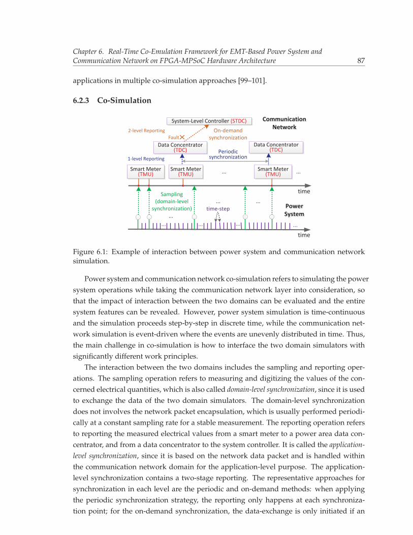
Chapter 6. Real-Time Co-Emulation Framework for EMT-Based Power System andCommunication Network on FPGA-MPSoC Hardware Architecture 87
applications in multiple co-simulation approaches [99–101].
6.2.3 Co-Simulation
Fault
...
time-step
... ... ...
PowerSystemPower System
CommunicationNetwork
Communication Network
...
...
Smart Meter(TMU)
Sampling(domain-level
synchronization)
Smart Meter(TMU)
Smart Meter(TMU)
Data Concentrator(TDC)
Data Concentrator(TDC)Periodic
synchronization
System-Level Controller (STDC)
...
On-demand synchronization
...
1-level Reporting
time
time
...
2-level Reporting
Figure 6.1: Example of interaction between power system and communication networksimulation.
Power system and communication network co-simulation refers to simulating the powersystem operations while taking the communication network layer into consideration, sothat the impact of interaction between the two domains can be evaluated and the entiresystem features can be revealed. However, power system simulation is time-continuousand the simulation proceeds step-by-step in discrete time, while the communication net-work simulation is event-driven where the events are unevenly distributed in time. Thus,the main challenge in co-simulation is how to interface the two domain simulators withsignificantly different work principles.
The interaction between the two domains includes the sampling and reporting oper-ations. The sampling operation refers to measuring and digitizing the values of the con-cerned electrical quantities, which is also called domain-level synchronization, since it is usedto exchange the data of the two domain simulators. The domain-level synchronizationdoes not involves the network packet encapsulation, which is usually performed periodi-cally at a constant sampling rate for a stable measurement. The reporting operation refersto reporting the measured electrical values from a smart meter to a power area data con-centrator, and from a data concentrator to the system controller. It is called the application-level synchronization, since it is based on the network data packet and is handled withinthe communication network domain for the application-level purpose. The application-level synchronization contains a two-stage reporting. The representative approaches forsynchronization in each level are the periodic and on-demand methods: when applyingthe periodic synchronization strategy, the reporting only happens at each synchroniza-tion point; for the on-demand synchronization, the data-exchange is only initiated if an
Chapter 6. Real-Time Co-Emulation Framework for EMT-Based Power System andCommunication Network on FPGA-MPSoC Hardware Architecture 88
event of interest is detected, and under normal conditions the corresponding measure-ment values are regarded as unchanged. An example is shown in Fig. 6.1, it can be seenthat the domain-level synchronization is performed at a constant sampling rate; while thetwo stages of the application-level synchronization are performed using the periodic andon-demand strategies respectively.
6.3 Proposed Real-Time Co-Emulation (RTCE) Framework
Based on the co-simulation background, this section describes the architecture and workprinciples of the proposed hardware-based real-time co-emulator.
6.3.1 Motivation
To conclude from the state of the art, most leading research in this area is either builton existing simulators or the development of a middleware to interface simulators fromthe two domains; thus their performance is dramatically limited by the software envi-ronment and achieving fast simulation for large-scale cyber-physical power systems be-comes difficult. There comes an alternative strategy into mind that combines both pro-grammability and high-speed computation: hardware-based co-emulation. Furthermore,the real-time power system simulation has already been extensively carried on FPGA, andcommunication network functions such as Ethernet, TCP/IP are also available as vendorspecific IP cores or soft-codes built on FPGA. The multiprocessor system-on-chip (MP-SoC) [54] integrates the FPGA based programmable hardware logic and the ARM� basedmulti-core processor systems within one platform, which enable complex embedded ap-plications to be developed. So why not deploy FPGA-MPSoC platform for implementingpower-communication co-simulation? First, the FPGA has a large amount of hardwareprogrammable logic resources that can be customized by the engineer to achieve specificfunctions; secondly, there are rich I/O transceivers in FPGA that enable several proto-typing boards to be interconnected to extend the compute capability for real-time powersystem EMT emulation or for emulating real communication network functions. In addi-tion, the processors integrated on the FPGA chip (such as Microblaze processor in Xilinx�
FPGAs) or the additional ARM� based APU processors in the MPSoC board provide theability to develop monitor and control systems for the cyber-physical system. Thus in thiswork, a real-time co-emulation (RTCE) framework based on an integrated FPGA-MPSoChardware platform is proposed to take advantage of the above mentioned features.
6.3.2 RTCE Hardware Architecture
The top-level architecture of RTCE framework is shown in Fig. 6.2, wherein the powersystem EMT emulation and the communication network emulation are integrated on eachboard. In power system domain, each board emulates a subsystem of the entire system,
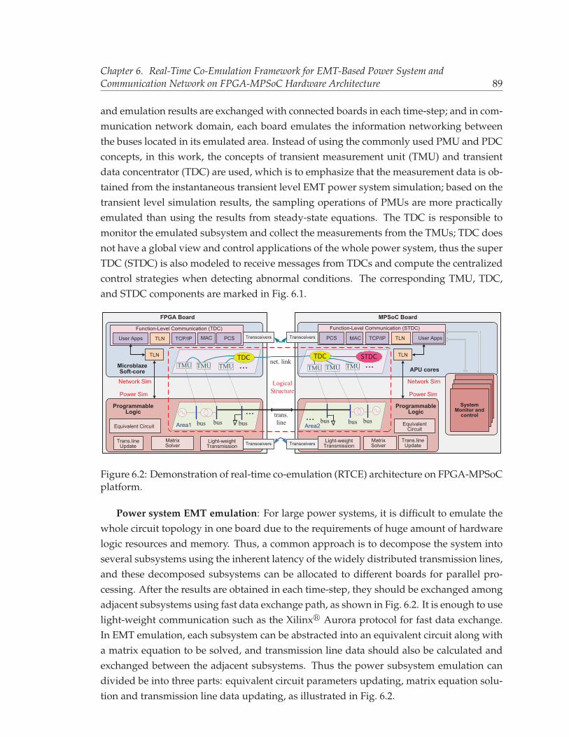
Chapter 6. Real-Time Co-Emulation Framework for EMT-Based Power System andCommunication Network on FPGA-MPSoC Hardware Architecture 89
and emulation results are exchanged with connected boards in each time-step; and in com-munication network domain, each board emulates the information networking betweenthe buses located in its emulated area. Instead of using the commonly used PMU and PDCconcepts, in this work, the concepts of transient measurement unit (TMU) and transientdata concentrator (TDC) are used, which is to emphasize that the measurement data is ob-tained from the instantaneous transient level EMT power system simulation; based on thetransient level simulation results, the sampling operations of PMUs are more practicallyemulated than using the results from steady-state equations. The TDC is responsible tomonitor the emulated subsystem and collect the measurements from the TMUs; TDC doesnot have a global view and control applications of the whole power system, thus the superTDC (STDC) is also modeled to receive messages from TDCs and compute the centralizedcontrol strategies when detecting abnormal conditions. The corresponding TMU, TDC,and STDC components are marked in Fig. 6.1.
Function-Level Communication (TDC)
Transceivers
MicroblazeSoft-core
Trans.lineUpdate
Equivalent Circuit
MatrixSolver
TCP/IP
trans.line
... ...
net. link...
bus bus bus bus bus bus
TDCTMU TMU TMU
TDCTMU TMU TMU
STDC
FPGA Board
Area1 Area2
...LogicalStructure
Transceivers
Transceivers
MAC PCS
Light-weightTransmission
Light-weightTransmission
ProgrammableLogic
MPSoC Board
Function-Level Communication (STDC)
TCP/IPMACPCS
SystemMonitor andcontrol
EquivalentCircuit
Trans.lineUpdate
MatrixSolver
TransceiversUser Apps User AppsTLN
TLN TLN
TLN
APU cores
ProgrammableLogic
Power Sim
Network Sim
Power Sim
Network Sim
Figure 6.2: Demonstration of real-time co-emulation (RTCE) architecture on FPGA-MPSoCplatform.
Power system EMT emulation: For large power systems, it is difficult to emulate thewhole circuit topology in one board due to the requirements of huge amount of hardwarelogic resources and memory. Thus, a common approach is to decompose the system intoseveral subsystems using the inherent latency of the widely distributed transmission lines,and these decomposed subsystems can be allocated to different boards for parallel pro-cessing. After the results are obtained in each time-step, they should be exchanged amongadjacent subsystems using fast data exchange path, as shown in Fig. 6.2. It is enough to uselight-weight communication such as the Xilinx� Aurora protocol for fast data exchange.In EMT emulation, each subsystem can be abstracted into an equivalent circuit along witha matrix equation to be solved, and transmission line data should also be calculated andexchanged between the adjacent subsystems. Thus the power subsystem emulation candivided be into three parts: equivalent circuit parameters updating, matrix equation solu-tion and transmission line data updating, as illustrated in Fig. 6.2.
Chapter 6. Real-Time Co-Emulation Framework for EMT-Based Power System andCommunication Network on FPGA-MPSoC Hardware Architecture 90
Communication network emulation: Since each FPGA/MPSoC board has limited I/Oresources and soft-processors, it can only operate as one network device. However, the net-work nodes (TMUs) in a smart grid can even have the same number as the buses, so it isimpossible to emulate all of the network nodes with bit-level details in hardware and ob-tain the correct transmission parameters between each TMU and STDC. Thus in this work,RTCE emulates the communication network with the two-level model: transmission-levelnetworking and function-level networking. The transmission-level networking is used tomodel the end-to-end packet transmission characteristics such as delay and loss, whilethe function-level networking is used to emulate the TDCs and model the specific net-work functions or protocols such as Ethernet or TCP/IP. The transmission-level emulationis inspired by work [102], which simply models individual network components such asrouters, hosts, links, and protocols with specific abstractions rather than completely imple-menting all the details to avoid complex hardware-based networking executions that arenot concerned in power system analysis. In this work, the transmission-level networkingmodels all of the transmission characteristics between TMUs and TDCs and between TDCsand STDC using parameters such as the link losses and delays, which can be obtainedthrough software simulators such as NS-2/3. The function-level networking is carried outdirectly on the I/O resources of FPGA/MPSoC boards, because the physical coding sub-layer (PCS) and media access controller (MAC) functions can be implemented using hard-ware logic resources, and the Internet protocol (IP) or other upper network layer functions(TCP, UDP, etc.) can run in the soft-processors (such as Xilinx� MicroBlaze) to handle thecomplex control tasks such as routing, connection establishment and flow control.
As shown in Fig. 6.2, each TMU receives the measurement from power system em-ulation as the sampling operation, and then sends the data packet to the correspondingfunction-level TDC module via the transmission-level networking (TLN) module as thereporting operation. Then the TDCs send data packets to the function-level STDC modulevia the real-world communication link if detecting abnormal conditions, but still need topass the TLN module in the function-level networking to emulate the transmission processbetween the TDC and STDC since TDCs/STDC are not directly connected in practical net-work. Using this method, the specific network functionalities can be emulated to observethe interaction between power and communication domains, while the detailed transmis-sion processes between TMUs, TDCs and the STDC are simplified and abstracted as crucialand practical transmission parameters.
Co-emulation: In each board, power system EMT emulation and communication net-work emulation run concurrently. Thus, the data exchange and synchronization betweenthe two domains are simplified: the results of power system emulation in each bus andeach time-step can be output to the network emulation module directly without any de-lays to emulate the sampling process of the TMU in a single process bus. That means, atevery hardware clock the results of the two domains can be exchanged within the FPGA
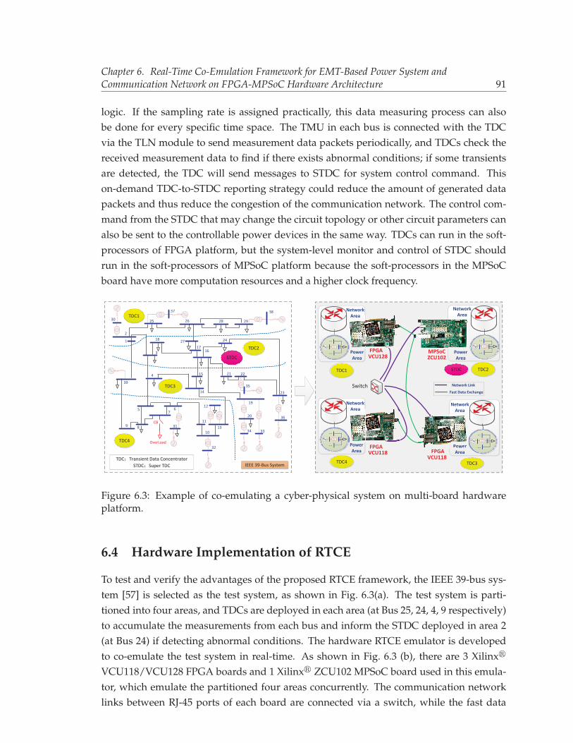
Chapter 6. Real-Time Co-Emulation Framework for EMT-Based Power System andCommunication Network on FPGA-MPSoC Hardware Architecture 91
logic. If the sampling rate is assigned practically, this data measuring process can alsobe done for every specific time space. The TMU in each bus is connected with the TDCvia the TLN module to send measurement data packets periodically, and TDCs check thereceived measurement data to find if there exists abnormal conditions; if some transientsare detected, the TDC will send messages to STDC for system control command. Thison-demand TDC-to-STDC reporting strategy could reduce the amount of generated datapackets and thus reduce the congestion of the communication network. The control com-mand from the STDC that may change the circuit topology or other circuit parameters canalso be sent to the controllable power devices in the same way. TDCs can run in the soft-processors of FPGA platform, but the system-level monitor and control of STDC shouldrun in the soft-processors of MPSoC platform because the soft-processors in the MPSoCboard have more computation resources and a higher clock frequency.
37
25
2
1
30
39
9 8
765
4
3110
11
12
13
15
163
18
17
26
27
28 29
24
19
20
32
34 33
21 22
35
23
36
38
14
OverLoad
TDC3
TDC1
TDC2
TDC4
STDC
NetworkArea
PowerArea
MPSoC
FPGAFPGA
TDC4 TDC3TDC Transient Data Concentrator
STDC Super TDCTDC Transient Data Concentrator
STDC Super TDC IEEE 39-Bus System
...
...
...
NetworkArea
PowerArea
...
...
...
STDC TDC2
NetworkArea
PowerArea
...
...
...
NetworkArea
PowerArea
FPGA
TDC1
...
...
...
Network LinkFast Data Exchange
VCU128
VCU118VCU118
ZCU102
CB
Switch
Area
Power
Figure 6.3: Example of co-emulating a cyber-physical system on multi-board hardwareplatform.
6.4 Hardware Implementation of RTCE
To test and verify the advantages of the proposed RTCE framework, the IEEE 39-bus sys-tem [57] is selected as the test system, as shown in Fig. 6.3(a). The test system is parti-tioned into four areas, and TDCs are deployed in each area (at Bus 25, 24, 4, 9 respectively)to accumulate the measurements from each bus and inform the STDC deployed in area 2(at Bus 24) if detecting abnormal conditions. The hardware RTCE emulator is developedto co-emulate the test system in real-time. As shown in Fig. 6.3 (b), there are 3 Xilinx�
VCU118/VCU128 FPGA boards and 1 Xilinx� ZCU102 MPSoC board used in this emula-tor, which emulate the partitioned four areas concurrently. The communication networklinks between RJ-45 ports of each board are connected via a switch, while the fast data
Chapter 6. Real-Time Co-Emulation Framework for EMT-Based Power System andCommunication Network on FPGA-MPSoC Hardware Architecture 92
exchange links for power system emulation are connected on the SFP/SFP+ ports via the10G optical fiber. The detailed hardware block design in each board is shown in Fig. 6.4.
6.4.1 Multi-Board EMT Emulation
In this work, the applied power equipment models (synchronous machine, power trans-former, transmission line and loads, etc.) are just the same as those of PSCAD/EMTDC�
[12] for verification. For real-time multi-board EMT emulation, the power system is usu-ally partitioned by the long transmission lines. Then the fast data exchange path is re-quired to exchange the transmission line model data among adjacent subsystems. In thiswork, the lightweight communication module is used: Xilinx� 64-bit Aurora core. Insteadof using the complex communication functionalities such as the Ethernet protocol, the sim-ple high-speed Aurora communication core enables direct data transfer through differenttypes of transceivers on FPGA/MPSoC boards with up to 10Gb/s speed.
To interact with the communication networking emulation, the abnormal conditiondetection is the prerequisite to determine the data packets generation. State estimator isusually used to predict the next state variable values and be compared with the real valueto determine if the system is running in control. For transient-level analysis of this work,the local truncation error (LTE) is used to estimate the perturbation, and the abnormalcondition is found once the LTE or the measured current and voltage exceed the prede-termined threshold. After the main conductance matrix is solved in each time-step, thestate variables of linear equipment are obtained, and then the LTE of the nth time-step iscomputed for the linear equipment, given by [25]:
LTE(tn) ≈ Cp+1Δtp+1n (p+ 1)! g[tn, ..., tn−1−p] (6.1)
where Cp+1 is the error constant of a specific discretization method, p is the order, andg[tn−1, ..., tn−1−k] can be calculated as:
g(tn−1) = xn−1 (6.2)
g[tn−1, ..., tn−k] =g[tn−1, ..., tn−k+1]− g[tn−2, ..., tn−k]
tn−1 − tn−k(6.3)
For the subsystems where nonlinear equipment exists, the iterative approach is involved.The standard method is to first use an explicit method or interpolation polynomial (calledthe predictor) to compute a candidate value of the state variable to be solved, and then useit as the initial solution to apply Newton’s method for the implicit integrator (called thecorrector) until convergence is achieved. Then the LTE can be estimated by comparing theinitial solution x0n and final solution xn [25]:
LTE(tn) ≈ Cp+1
1− Cp+1(xn − x0n) (6.4)
Chapter 6. Real-Time Co-Emulation Framework for EMT-Based Power System andCommunication Network on FPGA-MPSoC Hardware Architecture 93
6.4.2 Communication Protocol and Implementation
In order to practically emulate the communication network, the standardized communica-tion protocol, IEC 61850 - Communication Networks and Systems in Substations [103], isapplied in this work. IEC 61850 is used to manage the large number of communication de-vices. The existing communication protocols such as the Ethernet, TCP/IP typically definehow data bytes are transmitted on the wire, however, they did not specify the applicationlayer data organization. The 61850 model defines how the application data bits should bearranged and how the created data items/objects and services are mapped to any otherexisting under layer protocols that can meet the service requirements. In this work, allthe measurement data packets are encapsulated based the IEC 61850 standard that defineshow to transmit synchrophasor information according to IEEE C37.118 [104].
In the communication network emulation, each bus is alligned with a TMU, which isable to digitize the base measurement quantities at the source and transmit the resultingsample values to the TDC. The measurement data includes voltages, currents, and somestatus information (LTE). As introduced in Section 6.3.2, in RTCE architecture the data istransferred from power emulation to communication networking emulation in each time-step to do real-time EMT analysis, which means the sampling rate of TMU is related tothe actually applied time-step size. Different from the TMU measurement gathering thatdoes not involve network packet generation, the TDC collects data from the TMUs in itsarea based on a specific reporting rate. In this work, the reporting rate from TMU to TDCis set at 60Hz. As mentioned before, each TDC is required to compare the LTE, currentor voltage with the specific threshold; once the measurement exceeds the threshold, theabnormal condition is detected and then it is responsible to create a measurement datapacket to be sent to the STDC.
Transmission-level networking. The data packet networking is achieved in two modes:transmission-level networking and function-level networking. In the transmission-levelemulation, the transmission process between TMUs and the TDC and between TDCs andthe STDC is modeled as bandwidth, communication delay and loss rate. The transmission-level networking is implemented in the soft-processor of FPGA/MPSoC boards, becausethe transmission parameters can be flexibly configured in software without modification ofthe hardware design. As illustrated in Fig. 6.4, for example, if the TMU in Bus 6 generatesa packet to be sent to the TDC at Bus 9, then the data packet is generated in the hardwaremodule and then is sent to the soft-processor and passes the TLN function; and if the TDC(run as the function-level networking module) at Bus 9 detects an abnormal condition andsend a data packet to the STDC at Bus 24, the packet needs to first pass the TLN func-tion in the application layer of TCP/IP stack and then be sent to the lower TCP/IP andMAC layer. The implementation of the TLN function is quite straightforward: based onthe Xilinx� timer() function, the TLN function detects the source and destination of the in-put packet and searches for the corresponding end-to-end transmission delay; then, after

Chapter 6. Real-Time Co-Emulation Framework for EMT-Based Power System andCommunication Network on FPGA-MPSoC Hardware Architecture 94
the delay outputs the input data packet. The real communication delay is related to thedistance and hops between the source and destination, while the loss rate refers to the pos-sibility of an unsuccessful transmission process. In this implementation, the values chosenfor the delay and loss are determined based on the testing results from the real networksimulator NS-3 [105].
RJ45
Xilinx 1G/2.5G High Speed Ethernet Subsystem
GTH/GTY Transceivers
Ethernet PCS/PMA
AXI Ethernet MAC
AXI DMAAXI Interconnect
DDRMemory
MemoryInterface
FPGA MicroBlaze/MPSoC APU
Ethernet Driver
lwIP TCP/IP Stack
User Application(IEC61850)
AXI Interface
Stream Interface
Memory BlockMemoryInterface
Fast Data ExchangeXilinx Aurora Core
TMU MeasurementLTE Update Packet Generate ...
Network Data PathControl Command Path
Transmission-LevelNetworking (TLN) Measurement Data
CircuitUpdate
History ValueUpdate
MatrixSolver
Tran.Line
PowerSimulation
HardwareResource
DMA Driver
TLN
Figure 6.4: Illustration of detailed block design on a single FPGA/MPSoC board.
Function-level networking. For function-level communication network emulation,the high-level view is shown in Fig. 6.4. The Xilinx� 1G/2.5G High Speed Ethernet Sub-system core is used to implement the Media Access Controller (MAC) with a Physical Cod-ing Sublayer (PCS) based on the hardware logic and I/O resources. The upper networklayer functions are implemented in the Lightweight IP (lwIP) stack [106], which is an opensource TCP/IP networking stack for embedded systems and is available in the Xilinx�
programming tools. The Xilinx� Software Development Kit (SDK) provides lwIP softwarecustomized to run on various embedded systems that can be MicroBlaze soft-processor inFPGA chip or the ARM�-based SoC devices. Through the lwIP application programminginterface, users can add networking capability to an embedded system. Since the echoserver application that can create a TCP connection and sets up a callback on a connectionbeing accepted is already provided by Xilinx� SDK, the IEC 61850 protocol and data en-capsulation are implemented based on the existing echo server code to achieve the specificcommunication patterns of smart grid.
The function-level networking data path is marked as green arrows in Fig. 6.4, whichis achieved by the stream interface between direct memory access (DMA) module andEthernet module; the control command path that is used to send control commands fromthe controller in the soft-processor to the power emulation module is marked as red ar-rows in Fig. 6.4, which is achieved though the memory interface between DMA moduleand the block memory; the measurement data path that is used to send measurementdata from each TMU to the TDC is marked as the purple arrows, which is transmitted via
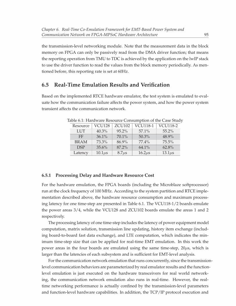
Chapter 6. Real-Time Co-Emulation Framework for EMT-Based Power System andCommunication Network on FPGA-MPSoC Hardware Architecture 95
the transmission-level networking module. Note that the measurement data in the blockmemory on FPGA can only be passively read from the DMA driver function; that meansthe reporting operation from TMU to TDC is achieved by the application on the lwIP stackto use the driver function to read the values from the block memory periodically. As men-tioned before, this reporting rate is set at 60Hz.
6.5 Real-Time Emulation Results and Verification
Based on the implemented RTCE hardware emulator, the test system is emulated to eval-uate how the communication failure affects the power system, and how the power systemtransient affects the communication network.
Table 6.1: Hardware Resource Consumption of the Case StudyResource VCU128 ZCU102 VCU118-1 VCU118-2
LUT 40.3% 95.2% 57.1% 55.2%FF 36.1% 70.1% 50.3% 48.9%
BRAM 73.3% 86.9% 77.4% 75.5%DSP 35.6% 87.2% 64.1% 62.8%
Latency 10.1μs 8.7μs 16.2μs 13.1μs
6.5.1 Processing Delay and Hardware Resource Cost
For the hardware emulation, the FPGA boards (including the Microblaze softprocessor)run at the clock frequency of 100 MHz. According to the system partition and RTCE imple-mentation described above, the hardware resource consumption and maximum process-ing latency for one time-step are presented in Table 6.1. The VCU118-1/2 boards emulatethe power areas 3/4, while the VCU128 and ZCU102 boards emulate the areas 1 and 2respectively.
The processing latency of one time-step includes the latency of power equipment modelcomputation, matrix solution, transmission line updating, history item exchange (includ-ing board-to-board fast data exchange), and LTE computation, which indicates the min-imum time-step size that can be applied for real-time EMT emulation. In this work thepower areas in the four boards are emulated using the same time-step, 20μs, which islarger than the latencies of each subsystem and is sufficient for EMT-level analysis.
For the communication network emulation that runs concurrently, since the transmission-level communication behaviors are parameterized by real emulator results and the function-level emulation is just executed on the hardware transceivers for real world network-ing, the communication network emulation also runs in real-time. However, the real-time networking performance is actually confined by the transmission-level parametersand function-level hardware capabilities. In addition, the TCP/IP protocol execution and
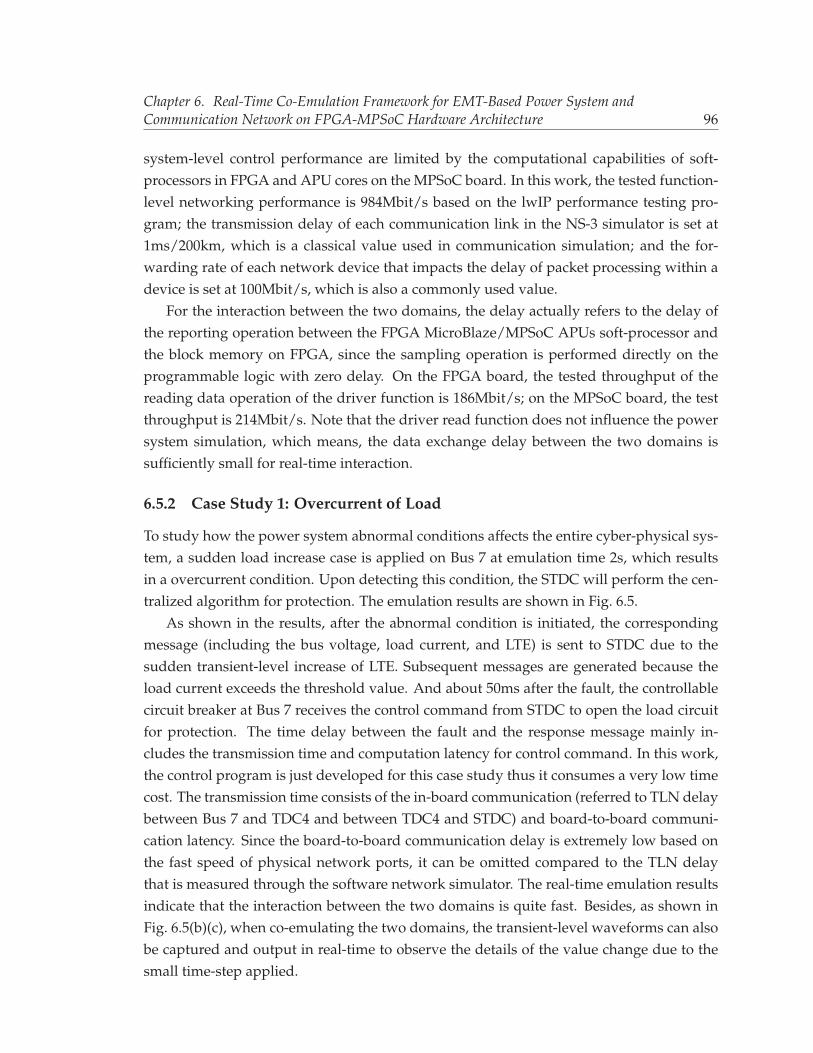
Chapter 6. Real-Time Co-Emulation Framework for EMT-Based Power System andCommunication Network on FPGA-MPSoC Hardware Architecture 96
system-level control performance are limited by the computational capabilities of soft-processors in FPGA and APU cores on the MPSoC board. In this work, the tested function-level networking performance is 984Mbit/s based on the lwIP performance testing pro-gram; the transmission delay of each communication link in the NS-3 simulator is set at1ms/200km, which is a classical value used in communication simulation; and the for-warding rate of each network device that impacts the delay of packet processing within adevice is set at 100Mbit/s, which is also a commonly used value.
For the interaction between the two domains, the delay actually refers to the delay ofthe reporting operation between the FPGA MicroBlaze/MPSoC APUs soft-processor andthe block memory on FPGA, since the sampling operation is performed directly on theprogrammable logic with zero delay. On the FPGA board, the tested throughput of thereading data operation of the driver function is 186Mbit/s; on the MPSoC board, the testthroughput is 214Mbit/s. Note that the driver read function does not influence the powersystem simulation, which means, the data exchange delay between the two domains issufficiently small for real-time interaction.
6.5.2 Case Study 1: Overcurrent of Load
To study how the power system abnormal conditions affects the entire cyber-physical sys-tem, a sudden load increase case is applied on Bus 7 at emulation time 2s, which resultsin a overcurrent condition. Upon detecting this condition, the STDC will perform the cen-tralized algorithm for protection. The emulation results are shown in Fig. 6.5.
As shown in the results, after the abnormal condition is initiated, the correspondingmessage (including the bus voltage, load current, and LTE) is sent to STDC due to thesudden transient-level increase of LTE. Subsequent messages are generated because theload current exceeds the threshold value. And about 50ms after the fault, the controllablecircuit breaker at Bus 7 receives the control command from STDC to open the load circuitfor protection. The time delay between the fault and the response message mainly in-cludes the transmission time and computation latency for control command. In this work,the control program is just developed for this case study thus it consumes a very low timecost. The transmission time consists of the in-board communication (referred to TLN delaybetween Bus 7 and TDC4 and between TDC4 and STDC) and board-to-board communi-cation latency. Since the board-to-board communication delay is extremely low based onthe fast speed of physical network ports, it can be omitted compared to the TLN delaythat is measured through the software network simulator. The real-time emulation resultsindicate that the interaction between the two domains is quite fast. Besides, as shown inFig. 6.5(b)(c), when co-emulating the two domains, the transient-level waveforms can alsobe captured and output in real-time to observe the details of the value change due to thesmall time-step applied.
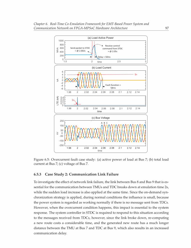
Chapter 6. Real-Time Co-Emulation Framework for EMT-Based Power System andCommunication Network on FPGA-MPSoC Hardware Architecture 97
(b) Load Current
(a) Load Active Power
Send packet to STDC≈ @ 2.002s
1.5 2 2.5 3time0
200400600800
1000
MVA
Receive control command from STDC
≈ @ 2.05s
Delay ≈ 50ms
time
-250
-150
-50050
150
250
kV
(c) Bus Voltage
1.98 2 2.02 2.04 2.06 2.08 2.1 2.12 2.14-6-4-20246
kA
1.98 2 2.02 2.04 2.06 2.08 2.1 2.12 2.140
0.10.20.30.4
time
LTE(kA)
ξth
ξth
1.98 2 2.02 2.04 2.06 2.08 2.1 2.12 2.14
A B C
Fault Duration ≈ 58ms
Figure 6.5: Overcurrent fault case study: (a) active power of load at Bus 7; (b) total loadcurrent at Bus 7; (c) voltage of Bus 7.
6.5.3 Case Study 2: Communication Link Failure
To investigate the effect of network link failure, the link between Bus 8 and Bus 9 that is es-sential for the communication between TMUs and TDC breaks down at emulation time 2s,while the sudden load increase is also applied at the same time. Since the on-demand syn-chronization strategy is applied, during normal conditions the influence is small, becausethe power system is regarded as working normally if there is no message sent from TDCs.However, when the overcurrent condition happens, this impact is essential to the systemresponse. The system controller in STDC is required to respond to this situation accordingto the messages received from TDCs, however, since the link broke down, re-computinga new route costs a considerable time, and the generated new route has a much longerdistance between the TMU at Bus 7 and TDC at Bus 9, which also results in an increasedcommunication delay.
Chapter 6. Real-Time Co-Emulation Framework for EMT-Based Power System andCommunication Network on FPGA-MPSoC Hardware Architecture 98
(b) Load Current
(a) Load Active Power
1.5 2 2.5 3time0
200400600800
1000
MVA
Delay ≈ 120ms
1.98 2 2.02 2.04 2.06 2.08 2.1 2.12 2.14-6-4-20246
kA
ξth
Send packet to STDC≈ @ 2.002s
Receive control command from STDC
≈ @ 2.12s
time
Duration ≈ 128ms
Figure 6.6: Communication link failure case study: (a) active power of load at Bus 7; (b)total load current at Bus 7.
As shown in Fig. 6.6, the system is supposed to respond to the overcurrent conditioncaused by the sudden load change within a short delay, however, due to the transmissionlink failure, the system response becomes relatively slow. Since the link failure impacts thetransmission-level communication delay, the increased latency is actually obtained fromthe NS-3 simulator. From Fig. 6.6(b) it can be observed that the total duration of overcur-rent condition raises to 128ms, which greatly increases the duration of damage.
6.6 Summary
For fast co-simulation of cyber-physical systems, this work proposes to use the FPGA-MPSoC based hardware platform instead of the software-based architecture to conduct thesimulation. In the proposed real-time co-emulation (RTCE) framework, the power systemEMT emulation is carried out on programmable hardware units so that transients can becaptured in real-time; and the communication network emulation is modeled in abstrac-tion for transmission-level characteristics and directly conducted on real-world physicalports to form the specific networking functions, which can emulate the communicationnetworking in real-time. The power system and communication network emulation mod-ules are embedded within each FPGA/MPSoC board so that the data exchange and syn-chronization between the two domains are sufficiently fast for real-time interaction. TheIEEE 39-bus system test system is implemented and emulated on FPGA-MPSoC platform.The effect of power system faults and communication link faults are studied, and the real-time emulation results show the effectiveness of the RTCE emulator. The proposed RTCEframework can be utilized for the study of emerging cyber-physical systems as well as fastemulation of test systems.
7Heterogeneous Real-Time Co-Emulation forCommunication-Enabled Global Control of
AC/DC Grid Integrated with RenewableEnergy
The information and communication technologies (ICTs) are increasingly merging withthe conventional power systems. For the design and development of modern AC/DCgrids with integrated renewable energy sources, the system-level control schemes withICTs involved should be evaluated in a co-simulation framework. In this chapter, a het-erogeneous hardware real-time co-emulator composed of FPGAs, many-core GPU, andmulti-core CPU devices is proposed to study the communication-enabled global controlschemes of hybrid AC/DC networks. The electromagnetic transient (EMT) power systememulation is conducted on the Xilinx� FPGA boards to provide nearly continuous instan-taneous waveforms for cyber layer sampling; the communication layer is simulated onthe ARM� CPU cores of the embedded NVIDIA� Jetson platform for flexible computingand programming; and the control functions for modular multi-level converters are ex-ecuted on GPU cores of the Jetson� platform for parallel calculation. The data exchangebetween FPGAs and Jetson� is achieved via the PCI express interface, which simulates thesampling operation of the AC phasor measurement unit (PMU) and DC merging unit (DC-MU). The power overflow and DC fault cases are investigated to demonstrate the validityand effectiveness of the proposed co-emulation hardware architecture and global controlschemes.
99
Chapter 7. Heterogeneous Real-Time Co-Emulation for Communication-Enabled Global Controlof AC/DC Grid Integrated with Renewable Energy 100
7.1 Introduction
With the development of modern power systems, the information and communicationtechnologies (ICT) are increasingly involved in the control, protection and normal oper-ation of power system equipment and infrastructure, which enables the evolution of theso called cyber-physical system. In such a system, various power equipment such as thegenerator, circuit breaker and power electronics converter can be controlled by the central-ized system-level controller through communication links [107]. The ICT-enabled powersystem operation and control needs to be evaluated in a co-simulation platform, whichcreates new challenges to the existing power system simulators [6, 43]. To simulate theentire behaviours of a cyber-physical system, the precise evaluation of power and commu-nication system is required while the interaction between the two domains should also beconsidered. The existing co-simulation research is mostly focused on the software-basedapproaches to combine the simulators in the two domains together by designing specificdata exchange interface and synchronization policies. Such software-based co-simulatorsmainly distinguish from each other by the type of power/communication system simu-lators used, the scheme of data exchange between the two domains, and the applicationscenarios, as discussed in Chapter 6.
On the other hand, the AC/DC grid with integrated renewable energies proposes chal-lenges to the system-level control for stability, security and fault recovery [108, 109]. Thepower generated by renewable generators such as offshore wind farms is transmitted tothe AC grid through the high voltage DC (HVDC) transmission, which should be con-trolled dynamically to match the generation and consumption. The existing AD/DC con-trol schemes mostly focused on the control algorithm for a single modular multilevel con-verter (MMC) [110, 111], or the control strategy in a small scale system without communi-cation networks involved [112–114]. However, the local measurement based control is notoptimized in the system-scale and easily delayed without a global view [115]. The cyberlayer creates the required capabilities to perform the global measurement and control, andICT-enabled power electronic converters that play important roles for power flow controlcan also receive the control command from the system-level controller to change the cor-responding parameters. Some utilities/consultants have used real time simulations withactually communication systems implemented in their labs in planning stages for complexcontrol schemes for remedial action scheme for stability enhancing control. This type ofcontrol for the large scale AC/DC grid with integrated renewable energies should also beevaluated in terms of system stability, but few works have been concentrated on this topicand no integrated simulation platforms that contain both the power system and commu-nication network simulation have been developed.
Based on the above observations, this work proposes an heterogeneous real-time EMT-based power and communication system co-emulator realized on multiple Jetson� andFPGA platforms for global control of hybrid AC/DC networks. The NVIDIA� Jetson AGX
Chapter 7. Heterogeneous Real-Time Co-Emulation for Communication-Enabled Global Controlof AC/DC Grid Integrated with Renewable Energy 101
Xavier embedded platform [116] is an artificial intelligence (AI) computer for autonomousmachines, delivering the performance of a 512-core GPU workstation within an embeddedmodule, which can perform heavy computation tasks. Taking advantage of the PCI express(PCIe) interface based connection between Jetson� and the FPGA, a complete hardwaresolution is developed to provide all the required capabilities for cyber-physical systemco-emulation. The contributions of this work are summarized as follows:
1. The EMT-based power system emulation is executed on FPGA boards with a mi-crosecond level time-step, which can provide a nearly continuous measurement tothe AC and DC sampling unit; the MMC converter control functions and commu-nication modules run on the Jetson� embedded platform, which perform fast andflexible computation for complex tasks;
2. The interaction between the two domains are emulated in a realistic way: powersystem measurement data sampling and converter controller sampling operation isachieved via the read operation from the FPGA memory, and the control and protec-tion commands are pushed to the power system emulation via the write operation tothe FPGA memory;
3. Based on the proposed heterogeneous co-emulation architecture, the global controlschemes are studied on the AC/DC grid integrated with wind farms. By utilizingthe communication network to perform global control strategies with fast responses,the influence of power overflow and DC fault can be reduced efficiently.
7.2 ICT-Enabled Hybrid AC/DC Grid
This section introduces the AC/DC test power system with integrated renewable energies,the corresponding communication network, and the ICT-enabled power equipment.
7.2.1 Hybrid AC/DC Power System
To investigate the global control and protection of modern power systems, a hybrid AC/DCgrid composed of onshore and offshore generation, AC and DC transmission, AC/DCand DC-DC converters as well as renewable energy sources is required. In this work, theAC/DC grid composed of an onshore IEEE 39-bus system [117], a subsystem of the CIGREB4 DC test grid [117] and two offshore wind farms is chosen as the test system, which canemulate a modern AC/DC power system practically. The CIGRE DC grid consists of threeinterconnected DC systems (DCSs) called DCS1, DCS2, and DCS3, and the bipole HVDCmeshed grid DCS3 with ±200kV is selected for DC test system, as shown in Fig. 7.1. TheMMC converter topology is applied to the AC/DC converters. The offshore wind farmsare responsible to power generation, and the generated power is transmitted to the ACgrid through the AC/DC and DC/AC conversion. Such a complex AC/DC power system
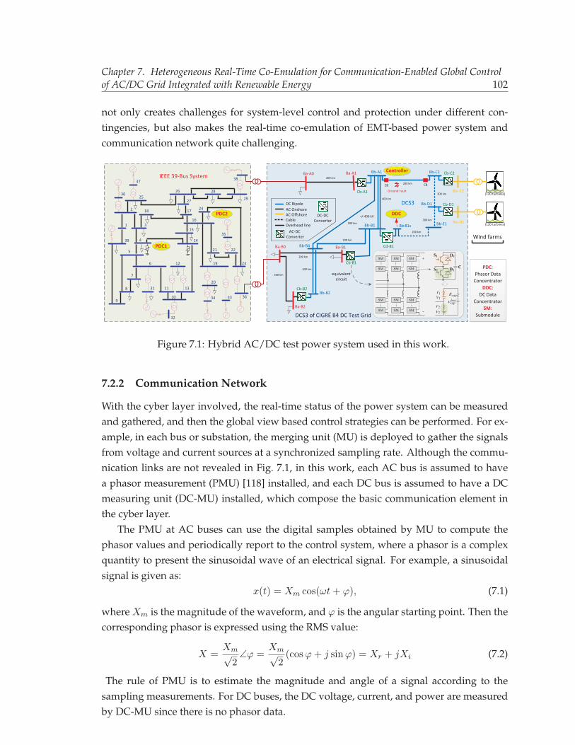
Chapter 7. Heterogeneous Real-Time Co-Emulation for Communication-Enabled Global Controlof AC/DC Grid Integrated with Renewable Energy 102
not only creates challenges for system-level control and protection under different con-tingencies, but also makes the real-time co-emulation of EMT-based power system andcommunication network quite challenging.
DCS3
Bb-B1
Ba-A1
Ba-B2
Ba-B1
Bb-B2
Bb-B4
Bb-B1s Bb-E1
Bb-D1
Bb-C2Bb-A1Ba-A0
200 km
200 km
200 km
200 km
200 km
300 km
300 km
400 km
200 km
200 km
500 km
+/-400 kV
Cb-A1
Cb-C2
Cb-D1
Cb-B2
Cb-B1
Cd-B1Ba-B0
IEEE 39-Bus System
DCS3 of CIGRÉ B4 DC Test Grid
Wind farms
DC BipoleAC Onshore
AC OffshoreCableOverhead line
AC-DC Converter
DC-DC Converter
Bo-C2
Bo-D1
(120 turbines)
(120 turbines)
37
25
2
1
30
39
9
8
7
6
5
4
31
10
11
12
13
14
15
163
18 17
26
27
28
29
24
19
20
32
34 33
21 22
35
23
36
38
PDC1
PDC2 DDC
equivalent circuit
SM
SM
SM
SM
SM
SM
SM
SM
SM
SM
SM
SM
S1 D1
S2 D2
r1v1r2v2
Rcapvcaphist
+
-
C
... ... ...
... ... ...
Controller
CB CB
Ground Fault
PDC: Phasor Data
ConcentratorDDC:
DC Data Concentrator
SM: Submodule
Figure 7.1: Hybrid AC/DC test power system used in this work.
7.2.2 Communication Network
With the cyber layer involved, the real-time status of the power system can be measuredand gathered, and then the global view based control strategies can be performed. For ex-ample, in each bus or substation, the merging unit (MU) is deployed to gather the signalsfrom voltage and current sources at a synchronized sampling rate. Although the commu-nication links are not revealed in Fig. 7.1, in this work, each AC bus is assumed to havea phasor measurement (PMU) [118] installed, and each DC bus is assumed to have a DCmeasuring unit (DC-MU) installed, which compose the basic communication element inthe cyber layer.
The PMU at AC buses can use the digital samples obtained by MU to compute thephasor values and periodically report to the control system, where a phasor is a complexquantity to present the sinusoidal wave of an electrical signal. For example, a sinusoidalsignal is given as:
x(t) = Xm cos(ωt+ ϕ), (7.1)
where Xm is the magnitude of the waveform, and ϕ is the angular starting point. Then thecorresponding phasor is expressed using the RMS value:
X =Xm√2∠ϕ =
Xm√2(cosϕ+ j sinϕ) = Xr + jXi (7.2)
The rule of PMU is to estimate the magnitude and angle of a signal according to thesampling measurements. For DC buses, the DC voltage, current, and power are measuredby DC-MU since there is no phasor data.
Chapter 7. Heterogeneous Real-Time Co-Emulation for Communication-Enabled Global Controlof AC/DC Grid Integrated with Renewable Energy 103
The control system is built on the cyber layer, in which the local controllers and central-ized system-level control center are connected via specific control network architecturessuch as the tree-based topology and mesh topology. The local controller can be a phasordata concentrator (PDC) that collects AC phasor measurements from PMUs in its region,or a DC data concentrator (DDC) that collects DC measurements from DC-MUs. The mea-surement collection operation of PDC is performed using a specific reporting rate [118].In fact, the main function of the communication network is to provide a two-way com-munication between smart meters and controllers to modify the related circuit parametersaccording to the service requirements. In this work, two PDCs (PDC1 and PDC2) are de-ployed at AC Bus4 and Bus24, and one DDC is deployed at DC bus Bb-B1s, as shown inFig. 7.1. The system-level controller is deployed at Bb-A1.
7.2.3 ICT-Enabled Power System Equipment
In the conventional power system, the power equipment is generally controlled by elec-trical quantities locally. In cyber-physical power systems, the ICT-enabled devices canreceive control commands from remote controllers to change the corresponding parame-ters. By utilizing the ICT-enabled controllable power equipment, flexible strategies andfast response to faults can be realized. Typically, the AC/DC circuit breakers (CBs) areICT-enabled for protection. For example, when a DC line ground fault is detected by aDC breaker, the line could be isolated by the DC breaker immediately; but the correspond-ing fault information is required to be sent to the centralized controller for subsequentstability control. The communication functions are also increasingly deployed in gener-ator and controllable load for flexible power supply and load balancing. For example, ifthe power generated from a machine exceeds the consumption, the corresponding controlcommand from the control center can guide the machine to reduce power generation orjust close the supply for a period. Another important power system equipment is the con-verter in DC grid, which is typically controlled by the outer/inner loop control and mod-ulation schemes for DC voltage or power regulations. However, with ICT involved, thepower electronics converter can also receive the control command from remote controllersto change the values of regulated quantities according to system-level purpose [119].
7.3 Heterogenous Real-Time Co-Emulation Architecture on Mul-tiple Jetson�-FPGA Platform
Based on the above introduced aspects in cyber-physical power systems, this section de-scribes the proposed real-time co-emulation architecture on the Jetson�-FPGA embeddedplatform.
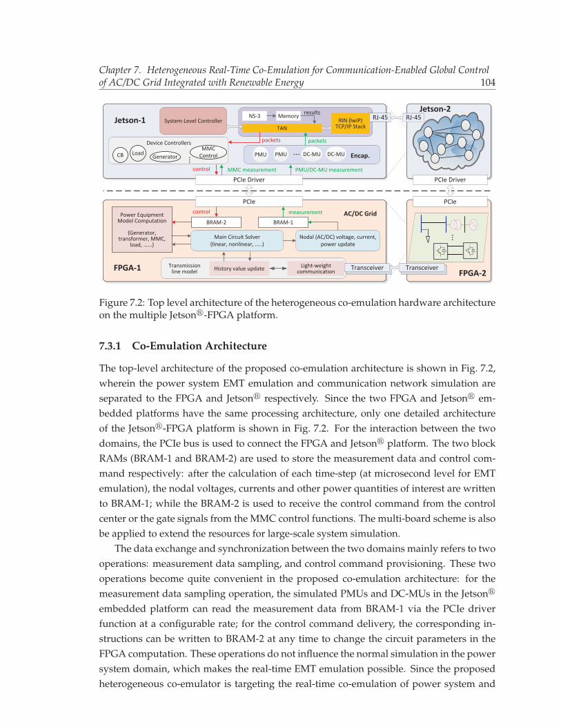
Chapter 7. Heterogeneous Real-Time Co-Emulation for Communication-Enabled Global Controlof AC/DC Grid Integrated with Renewable Energy 104
Light-weight communicationFPGA-1 FPGA-2
PCIe
PCIe Driver
PCIe
PCIe Driver
Jetson-1Jetson-2
RJ-45
History value update
...
BRAM-1
measurementcontrol
BRAM-2Power Equipment
Model Computation
(Generator, transformer, MMC,
load, …...)
control PMU/DC-MU measurement
PMU PMU ...LoadCB ...
Device Controllers
GeneratorMMC
Control
Transmission line model
Main Circuit Solver(linear, nonlinear, …..)
Nodal (AC/DC) voltage, current, power update
AC/DC Grid
packets
RJ-45
packets
MMC measurement
RIN (lwIP)TCP/IP StackTAN
NS-3 MemorySystem-Level Controller
Encap.
results
DC-MU DC-MU
TransceiverTransceiverTransceiver TransceiverTransceiverTransceiver
Figure 7.2: Top level architecture of the heterogeneous co-emulation hardware architectureon the multiple Jetson�-FPGA platform.
7.3.1 Co-Emulation Architecture
The top-level architecture of the proposed co-emulation architecture is shown in Fig. 7.2,wherein the power system EMT emulation and communication network simulation areseparated to the FPGA and Jetson� respectively. Since the two FPGA and Jetson� em-bedded platforms have the same processing architecture, only one detailed architectureof the Jetson�-FPGA platform is shown in Fig. 7.2. For the interaction between the twodomains, the PCIe bus is used to connect the FPGA and Jetson� platform. The two blockRAMs (BRAM-1 and BRAM-2) are used to store the measurement data and control com-mand respectively: after the calculation of each time-step (at microsecond level for EMTemulation), the nodal voltages, currents and other power quantities of interest are writtento BRAM-1; while the BRAM-2 is used to receive the control command from the controlcenter or the gate signals from the MMC control functions. The multi-board scheme is alsobe applied to extend the resources for large-scale system simulation.
The data exchange and synchronization between the two domains mainly refers to twooperations: measurement data sampling, and control command provisioning. These twooperations become quite convenient in the proposed co-emulation architecture: for themeasurement data sampling operation, the simulated PMUs and DC-MUs in the Jetson�
embedded platform can read the measurement data from BRAM-1 via the PCIe driverfunction at a configurable rate; for the control command delivery, the corresponding in-structions can be written to BRAM-2 at any time to change the circuit parameters in theFPGA computation. These operations do not influence the normal simulation in the powersystem domain, which makes the real-time EMT emulation possible. Since the proposedheterogeneous co-emulator is targeting the real-time co-emulation of power system and
Chapter 7. Heterogeneous Real-Time Co-Emulation for Communication-Enabled Global Controlof AC/DC Grid Integrated with Renewable Energy 105
communication network, the hybrid Jetson�-FPGA hardware platform is utilized, whichmay not be as flexible as the pure software-based co-simulator and more programmingeffort needs to be invested when the emulated test system changes.
7.3.2 Hybrid AC/DC Grid EMT Emulation
In this work, the EMT emulation is conducted for the power system, because it not onlycan capture the transient-level waveforms, but can also provide continuous signals dueto the small time-step sizes so that the measured data to PMUs and DC-MUs is accurateenough. Typically, real-time emulation can be achieved on FPGA boards even for large-scale AC/DC grids [120]. However, in co-emulation, the extra operations are introduced:writing measurement data to BRAM-1 and reading control command from BRAM-2. Thenumber of measured data is large if the electrical quantities of each bus are required, thenit costs a considerable latency to write data to BRAM-1 since in each clock cycle only onedata can be written. In this work, this operation is delayed for one time-step, which means,the results of the last time-step calculation are written to the BRAM-1 while the circuit iscomputed for the current time-step. Since the interval of sampling is larger than the time-step size of EMT emulation, the one time-step delay is acceptable. The same policy can beapplied to the read operations to achieve real-time EMT emulation.
When the multi-board solution is adopted, the power system is decomposed into sub-systems using the traveling-wave line model (TLM) or frequency-dependent line model(FDLM). Then the two ends of a transmission line can be computed in two FPGA boardsconcurrently and exchange their data after each time-step. This type of data exchangebetween the two FPGA boards should be executed via fast transmission protocol andtransceivers to ensure the transmission delay is minimized for real-time emulation.
7.3.3 Communication Network Emulation
The communication network is built on communication devices with specific protocols,thus the task of communication system simulation is to simulate the behaviour of net-work forwarding devices and transmission links. In the related works, various networksimulators such as NS-2/NS-3, OpenNet, OMNet++ have been utilized to conduct thenetwork-domain simulation. However, the existing solutions are not applicable to theproposed co-emulation architecture, because: 1) using the created virtual network, newinterfaces are required to be developed for synchronizing the measurement data, which istime-costly and make the real-time co-emulation infeasible; 2) for large-scale AC/DC testpower systems, hundreds of nodes need to be instantiated if each node is regarded witha PMU installed, then each node needs to receive the corresponding sampling data andgenerate data packets, which greatly increases the simulation latency.
Different from the pure network simulation that aims to investigate the packet trans-mission or test new protocols, the essential goal of the co-emulation is to study the in-
Chapter 7. Heterogeneous Real-Time Co-Emulation for Communication-Enabled Global Controlof AC/DC Grid Integrated with Renewable Energy 106
fluence of the cyber layer on the physical layer, i.e., how the power system is improvedunder the support of communication network. Therefore, the end-to-end communicationparameters such as the transmission latencies and packet losses are of the greatest concern.Based on this observation, in this work, the communication module is implemented in ahybrid manner as shown in Fig. 7.2: transmission abstraction based networking (TAN)and real network interface based networking (RIN). TAN on a Jetson� embedded plat-form is used for the networking within the corresponding power system area emulated onthe connected FPGA board, which reads the results from the NS-3 simulator in advanceand then uses the resulting transmission parameters to abstract the packet transmission.This simplification is to accelerate the co-emulation process to real-time, while the usedtransmission parameters obtained by the network simulator are also practical and reason-able. RIN is used for inter-board networking, which is executed on the real-world networkinterfaces of the Jetson� embedded platform to simulate the packet transmission betweendifferent power system areas. The measurement data packet generation function is also in-cluded in the architecture, which is used to simulate the behaviour of PMUs and DC-MUsthat sample measurement data from power system and encapsulate the measurement intonetwork packets to be sent to the PDC.
7.4 Hardware Implementation of Test System
The test system is implemented on the Jetson�-FPGA platform. Two Xilinx� VCU118FPGA boards and two NVIDIA� Jetson embedded platforms are utilized.
7.4.1 Heterogeneous Co-Emulator Hardware Resources and Set-Up
The Xilinx� VCU118 evaluation board provides a hardware environment for develop-ing and evaluating designs targeting the UltraScale+ XCVU9P-L2FLGA2104 device. TheVCU118 evaluation board provides features common to many evaluation systems, includ-ing the dual small form-factor pluggable (QSFP+) connector and sixteen-lane PCI expressinterface. The 16-lane PCIe edge connector performs data transfers at the rate of 8.0 GT/sfor Gen3 applications, and the XCVU9P-L2FLGA2104 device is deployed on the VCU118to support up to Gen3 x8 channels. The two quad (4-channel) QSFP+ (28 Gb/s) connectorsaccept 28 Gb/s QSFP+ optical modules. Each connector is housed within a single 28 Gb/sQSFP+ cage assembly.
The NVIDIA� Jetson embedded platforms provide the performance and power effi-ciency to run autonomous machines software. Each Jetson� embedded platform is a com-plete System-on-Module (SOM), with CPU, GPU, PMIC, DRAM, and flash storage—savingdevelopment time and money. The 512-core Volta GPU with tensor cores, the 8-core ARM�
v8.2 64-bit CPU, 32GB 256-bit memory, x8 PCIe interface and RJ45 gigabit ethernet inter-face enable the proposed heterogeneous co-emulation architecture to be completed imple-
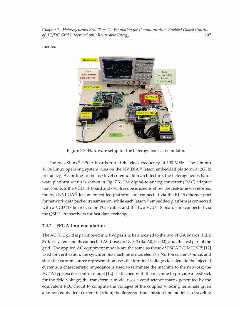
Chapter 7. Heterogeneous Real-Time Co-Emulation for Communication-Enabled Global Controlof AC/DC Grid Integrated with Renewable Energy 107
mented.
Oscilloscope
Xilinx® VCU118
Xilinx® VCU118
DAC Board
Nvidia® Jetson
Nvidia® Jetson
QSFP(Aurora based
Data Exchange)
QSFP
RJ45(Network Data
Packet Transmission)
PCIe
RJ45
Figure 7.3: Hardware setup for the heterogeneous co-emulator.
The two Xilinx� FPGA boards run at the clock frequency of 100 MHz. The Ubuntu18.04 Linux operating system runs on the NVIDIA� Jetson embedded platform at 2GHzfrequency. According to the top level co-emulation architecture, the heterogeneous hard-ware platform set up is shown in Fig. 7.3. The digital-to-analog converter (DAC) adapterthat connects the VCU118 board and oscilloscope is used to show the real-time waveforms;the two NVIDIA� Jetson embedded platforms are connected via the RJ-45 ethernet portfor network data packet transmission, while each Jetson� embedded platform is connectedwith a VCU118 board via the PCIe cable; and the two VCU118 boards are connected viathe QSFP+ transceivers for fast data exchange.
7.4.2 FPGA Implementation
The AC/DC grid is partitioned into two parts to be allocated to the two FPGA boards: IEEE39-bus system and its connected AC buses in DCS-3 (Ba-A0, Ba-B0), and, the rest part of thegrid. The applied AC equipment models are the same as those of PSCAD/EMTDC� [12]used for verification: the synchronous machine is modeled as a Norton current source, andsince the current source representation uses the terminal voltages to calculate the injectedcurrents, a characteristic impedance is used to terminate the machine to the network; theAC4A type exciter control model [12] is attached with the machine to provide a feedbackfor the field voltage; the transformer model uses a conductance matrix generated by theequivalent RLC circuit to compute the voltages of the coupled winding terminals givena known equivalent current injection; the Bergeron transmission line model is a traveling
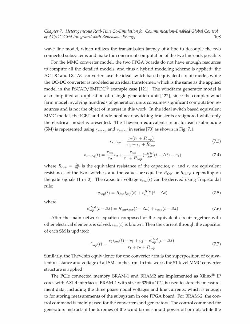
Chapter 7. Heterogeneous Real-Time Co-Emulation for Communication-Enabled Global Controlof AC/DC Grid Integrated with Renewable Energy 108
wave line model, which utilizes the transmission latency of a line to decouple the twoconnected subsystems and make the concurrent computation of the two line ends possible.
For the MMC converter model, the two FPGA boards do not have enough resourcesto compute all the detailed models, and thus a hybrid modeling scheme is applied: theAC-DC and DC-AC converters use the ideal switch based equivalent circuit model, whilethe DC-DC converter is modeled as an ideal transformer, which is the same as the appliedmodel in the PSCAD/EMTDC� example case [121]. The windfarm generator model isalso simplified as duplication of a single generation unit [122], since the complex windfarm model involving hundreds of generation units consumes significant computation re-sources and is not the object of interest in this work. In the ideal switch based equivalentMMC model, the IGBT and diode nonlinear switching transients are ignored while onlythe electrical model is presented. The Thevenin equivalent circuit for each submodule(SM) is represented using rsm,eq and vsm,eq in series [73] as shown in Fig. 7.1:
rsm,eq =r2(r1 +Rcap)
r1 + r2 +Rcap(7.3)
vsm,eq(t) =rsmr2
v2 +rsm
r1 +Rcap(vHist
cap (t−Δt)− v1) (7.4)
where Rcap = Δt2C is the equivalent resistance of the capacitor, r1 and r2 are equivalent
resistances of the two switches, and the values are equal to RON or ROFF depending onthe gate signals (1 or 0). The capacitor voltage vcap(t) can be derived using Trapezoidalrule:
vcap(t) = Rcapicap(t) + vHistcap (t−Δt) (7.5)
wherevHistcap (t−Δt) = Rcapicap(t−Δt) + vcap(t−Δt) (7.6)
After the main network equation composed of the equivalent circuit together withother electrical elements is solved, ism(t) is known. Then the current through the capacitorof each SM is updated:
icap(t) =r2ism(t) + v1 + v2 − vHist
cap (t−Δt)
r1 + r2 +Rcap(7.7)
Similarly, the Thevenin equivalence for one converter arm is the superposition of equiva-lent resistance and voltage of all SMs in the arm. In this work, the 51-level MMC converterstructure is applied.
The PCIe connected memory BRAM-1 and BRAM2 are implemented as Xilinx� IPcores with AXI-4 interfaces. BRAM-1 with size of 32bit×1024 is used to store the measure-ment data, including the three phase nodal voltages and line currents, which is enoughto for storing measurements of the subsystem in one FPGA board. For BRAM-2, the con-trol command is mainly used for the converters and generators. The control command forgenerators instructs if the turbines of the wind farms should power off or not; while the
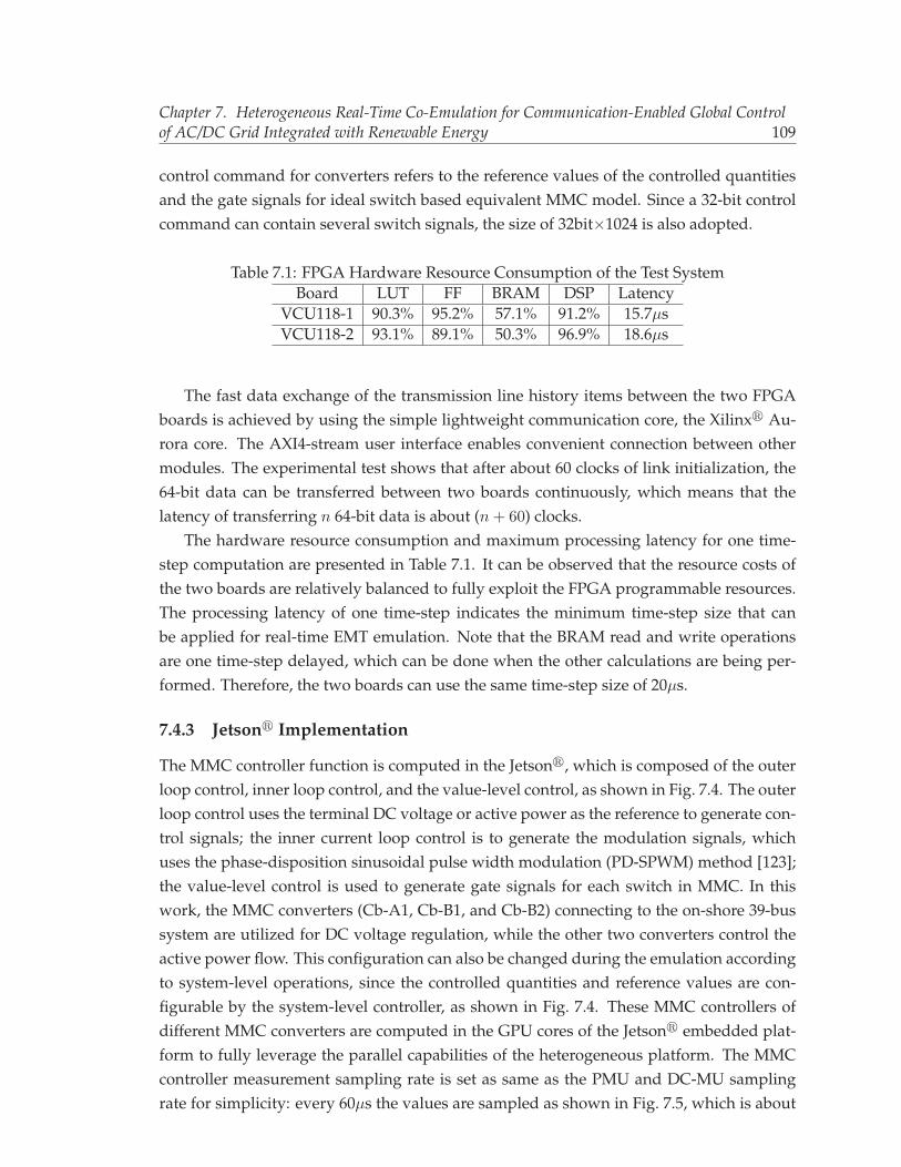
Chapter 7. Heterogeneous Real-Time Co-Emulation for Communication-Enabled Global Controlof AC/DC Grid Integrated with Renewable Energy 109
control command for converters refers to the reference values of the controlled quantitiesand the gate signals for ideal switch based equivalent MMC model. Since a 32-bit controlcommand can contain several switch signals, the size of 32bit×1024 is also adopted.
Table 7.1: FPGA Hardware Resource Consumption of the Test SystemBoard LUT FF BRAM DSP Latency
VCU118-1 90.3% 95.2% 57.1% 91.2% 15.7μsVCU118-2 93.1% 89.1% 50.3% 96.9% 18.6μs
The fast data exchange of the transmission line history items between the two FPGAboards is achieved by using the simple lightweight communication core, the Xilinx� Au-rora core. The AXI4-stream user interface enables convenient connection between othermodules. The experimental test shows that after about 60 clocks of link initialization, the64-bit data can be transferred between two boards continuously, which means that thelatency of transferring n 64-bit data is about (n+ 60) clocks.
The hardware resource consumption and maximum processing latency for one time-step computation are presented in Table 7.1. It can be observed that the resource costs ofthe two boards are relatively balanced to fully exploit the FPGA programmable resources.The processing latency of one time-step indicates the minimum time-step size that canbe applied for real-time EMT emulation. Note that the BRAM read and write operationsare one time-step delayed, which can be done when the other calculations are being per-formed. Therefore, the two boards can use the same time-step size of 20μs.
7.4.3 Jetson� Implementation
The MMC controller function is computed in the Jetson�, which is composed of the outerloop control, inner loop control, and the value-level control, as shown in Fig. 7.4. The outerloop control uses the terminal DC voltage or active power as the reference to generate con-trol signals; the inner current loop control is to generate the modulation signals, whichuses the phase-disposition sinusoidal pulse width modulation (PD-SPWM) method [123];the value-level control is used to generate gate signals for each switch in MMC. In thiswork, the MMC converters (Cb-A1, Cb-B1, and Cb-B2) connecting to the on-shore 39-bussystem are utilized for DC voltage regulation, while the other two converters control theactive power flow. This configuration can also be changed during the emulation accordingto system-level operations, since the controlled quantities and reference values are con-figurable by the system-level controller, as shown in Fig. 7.4. These MMC controllers ofdifferent MMC converters are computed in the GPU cores of the Jetson� embedded plat-form to fully leverage the parallel capabilities of the heterogeneous platform. The MMCcontroller measurement sampling rate is set as same as the PMU and DC-MU samplingrate for simplicity: every 60μs the values are sampled as shown in Fig. 7.5, which is about
Chapter 7. Heterogeneous Real-Time Co-Emulation for Communication-Enabled Global Controlof AC/DC Grid Integrated with Renewable Energy 110
278 samples per cycle (16.67kHz) for the 60Hz power system.
refdcV
dcV
refPP
PI
PI
dv
ωL
PI
dqabc
refdi
di
ωL
PIrefqi
qi
qv
Limiter abcm
abcdq
ABCsv
ABCsi abc
dq
PLL
Inner LoopControl
Value LevelControl
1 2ncapv
1 4ng
armi
DetermineInsertedSM
number
Sorting
Carrier
Gatesignals
Outer LoopControl
Controloptions
Ref.values
Figure 7.4: The ICT-enabled PD-SPWM MMC control scheme.
time...
time-step(20us)
... ... ...
FPGAFPGA
measure data
JetsonJetson
time
...
...
MMC Control/PMU,DC-MU
Sampling (16.67kHz)
MMC Control/PMU,DC-MU
MMC Control/PMU,DC-MU
PDC/DDC PDC/DDCperiodicreporting
(30Hz)
System-Level Controller
...
on-demand message
data packet
...
data packet
Figure 7.5: Demonstration of interaction between power system emulation and communi-cation network simulation.
The packet generation module uses the PCIe driver functions to read the measurementdata in BRAM-1 of the FPGA at the sampling rate. Then the corresponding phasors arecomputed using the measurement voltage and current, and the phasor data are encapsu-lated as the network packets and sent to the PDC functions with a reporting rate of 30Hz.This process is to simulate the measurement operation of PMUs and DC-MUs. The IEEEStd. C37.118.2 [90] primarily describes the presentation of synchrophasor data packet in abit-mapped format. The standardized communication protocol, IEC 61850 - Communica-tion Networks and Systems in Substations [103], also describes a similar approach to pre-sentation and has been mainly used in the communication between protection relays andcontrol systems. In this work, the bit-map of the packet follows IEC 61850. The PDC/DDCfunction checks the received phasor data or DC data to see if there are abnormal condi-
Chapter 7. Heterogeneous Real-Time Co-Emulation for Communication-Enabled Global Controlof AC/DC Grid Integrated with Renewable Energy 111
tions; and if abnormal conditions are detected, the corresponding messages are sent to thecenter system-level controller in an “on-demand” pattern, as shown in Fig. 7.5.
In the transmission abstraction based networking (TAN), the transmission process be-tween PMUs and PDCs and between PDCs and the system-level controller is handledbased on the resulting parameters: end-to-end communication delay and loss rate. Forexample, if the PMU at Bus 7 generates a data packet to be sent to the PDC at Bus 4, thenthe data packet is generated in packet generation module and then is sent to the PDCfunction by passing the TAN function. In this implementation, the values chosen for thedelay and loss are determined based on the testing results from the real network simulatorNS-3 [105]. The corresponding capabilities of the network devices and links are config-urable in the NS-3 simulator. In fact, there are two essential parameters in the NS-3 setupthat may affect the end-to-end transmission delay: the transmission delay of each link,and, the forwarding rate of each device. In this work, the forwarding rate of each deviceis set at 100Mbps, which is a common value for devices in cyber-physical systems; andthe transmission delay is set at 1ms/200km, which is also a practical value for the signaltransmission. Then the link delays of different transmission lines with different length arecomputed accordingly.
In the real network interface based networking (RIN), the light-weight IP (lwIP) stack[106] is installed. Through the lwIP application programming interface, users can addcustomized networking functions. In this work, the IEC 61850 packet format and dataencapsulation are implemented based on the existing echo server code to achieve the spe-cific communication patterns of cyber-physical systems. Since the TAN module uses theresulting end-to-end parameters output by NS-3 and the measurement sampling is alsoperformed using the system timer, the network simulation actually runs in real-time. Bycoordinating with the power system emulation, the real-time co-emulation can be achievedon the heterogeneous Jetson�-FPGA platform.
7.5 Real-Time Hardware Emulation Results for Communication-Enabled Global Control
Based on the implementation of the proposed hardware co-emulator, the global controlschemes for the AC/DC test power system is studied and emulated for the two cases:power overflow and DC fault protection. Since the existing co-simulators are not fullyopen-sourced and are implemented on disparate platforms, it is extremely difficult to eval-uate the test power system using the existing co-simulators for comparison. However, theemulation results and the proposed ICT-enabled global control scheme are still reasonabledue to the standard test power systems, commonly used power equipment EMT models,practical fault cases, and realistic control strategies.
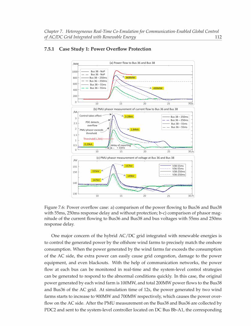
Chapter 7. Heterogeneous Real-Time Co-Emulation for Communication-Enabled Global Controlof AC/DC Grid Integrated with Renewable Energy 112
7.5.1 Case Study 1: Power Overflow Protection
(a) Power flow to Bus 36 and Bus 38
(b) PMU phasor measurement of current flow to Bus 36 and Bus 38
10 15 20 25 300
200
400
600
800
1000
10 15 20 25 300
1
2
/kA
/MW
/s
/s
Bus 38 - NoPBus 36 - NoP
Bus 36 – 250msBus 38 – 250ms
Bus 38 – 55msBus 36 – 55ms
Bus 36 – 250msBus 38 – 250ms
Bus 38 – 55msBus 36 – 55ms
Threshold(1.2kA)
PDC detectsoverflow
868MW
499MW
PMU phasor exceeds threshold
delay of reporting≈ 33ms
3.28kA
1.84kA
0.29kA
3
0.5
1.5
2.5
Control takes effect
10 15 20 25 30130
140
150
155 V38-55msV36-55msV38-250msV36-250ms
(c) PMU phasor measurement of voltage at Bus 36 and Bus 38
/s
/kV
157kV
155kV
149kV147kV
Figure 7.6: Power overflow case: a) comparison of the power flowing to Bus36 and Bus38with 55ms, 250ms response delay and without protection; b-c) comparison of phasor mag-nitude of the current flowing to Bus36 and Bus38 and bus voltages with 55ms and 250msresponse delay.
One major concern of the hybrid AC/DC grid integrated with renewable energies isto control the generated power by the offshore wind farms to precisely match the onshoreconsumption. When the power generated by the wind farms far exceeds the consumptionof the AC side, the extra power can easily cause grid congestion, damage to the powerequipment, and even blackouts. With the help of communication networks, the powerflow at each bus can be monitored in real-time and the system-level control strategiescan be generated to respond to the abnormal conditions quickly. In this case, the originalpower generated by each wind farm is 100MW, and total 200MW power flows to the Bus38and Bus36 of the AC grid. At simulation time of 12s, the power generated by two windfarms starts to increase to 900MW and 700MW respectively, which causes the power over-flow on the AC side. After the PMU measurement on the Bus38 and Bus36 are collected byPDC2 and sent to the system-level controller located on DC Bus Bb-A1, the corresponding
Chapter 7. Heterogeneous Real-Time Co-Emulation for Communication-Enabled Global Controlof AC/DC Grid Integrated with Renewable Energy 113
control commands that instruct the wind farms to decrease the generation are sent to thetwo wind farms; and the commands that change the reference values of power flows aresent to the converter Cb-C2 and Cb-D1.
This process was emulated on the heterogeneous hardware co-emulator, and the resultswith 55ms and 250ms response delay and without protection (NoP) are shown in Fig. 7.6.Note that the response delay is between the time when the PMU phasor magnitude ex-ceeded the threshold and the time when the corresponding power equipment received thecontrol command. The 55ms delay was obtained by the real-time co-emulation, whichincluded the reporting delay (30Hz, about 33ms), transmission delay (13ms), control com-mand generation delay, and the control taking effect delay. The 250ms delay is chosen tobe compared to the 55ms delay to show the influence of longer response, which can beregarded as the situation where a communication link fault happens and a larger responselatency is generated due to the latency of data packet re-routing. The waveforms of powerand current phasor magnitude in Fig. 7.6 are all from the view of PMUs and DC-MUs. Itcan be observed from Fig. 7.6(a) that without the system-level control, the power overflowcould cause huge increase of the power to Bus38 and Bus36.
For the case with protection, the PDC2 detected the current flow to Bus38 and Bus36,and the threshold of phasor magnitude (RMS value) is set at 1.2kA, which is 4 times ofthat under the normal condition. After the current phasor magnitude of PMU38 at Bus38exceeded the threshold, the PDC2 detected the abnormal condition after a reporting delay.In this case, since the 30Hz reporting rate is used, the reporting delay is at most 33ms.Then the PDC2 generated related data packets and sent to the controller via the communi-cation network. The total communication delay included the delay from PMU38 to PDC2,the delay from PDC2 to controller, and from controller to windfarm and converter Cb-C2/Cb-D1, which was about 13ms resulting from the NS-3 simulator. The system-levelcontroller held a global view of the system topology and made a decision that shut downsome turbines of the wind farms to reduce the generated power to 100MW and reducesthe reference values of the converters. From Fig. 7.6(b)(c) it can be observed that when thepower generated by the wind farms increased quickly, the impact of difference of responsedelay was amplified on the resulting current and voltage. Therefore, a small communica-tion delay can benefit the global stability. Besides, it can be also seen that after the controlcommand took effect, there was still a short increase of the current, because it took time torelease the power stored in the capacitors of MMC submodules.
7.5.2 Case Study 2: DC Fault Protection
The DC line ground fault is an important type of faults that can cause inreversible damagesto the converters and should be protected against prior to the commissioning of HVDCgrid. DC circuit breakers can be installed on the two ends of the DC lines, and they canisolate the fault when it is detected. The fast transient signal detection scheme [124] can be
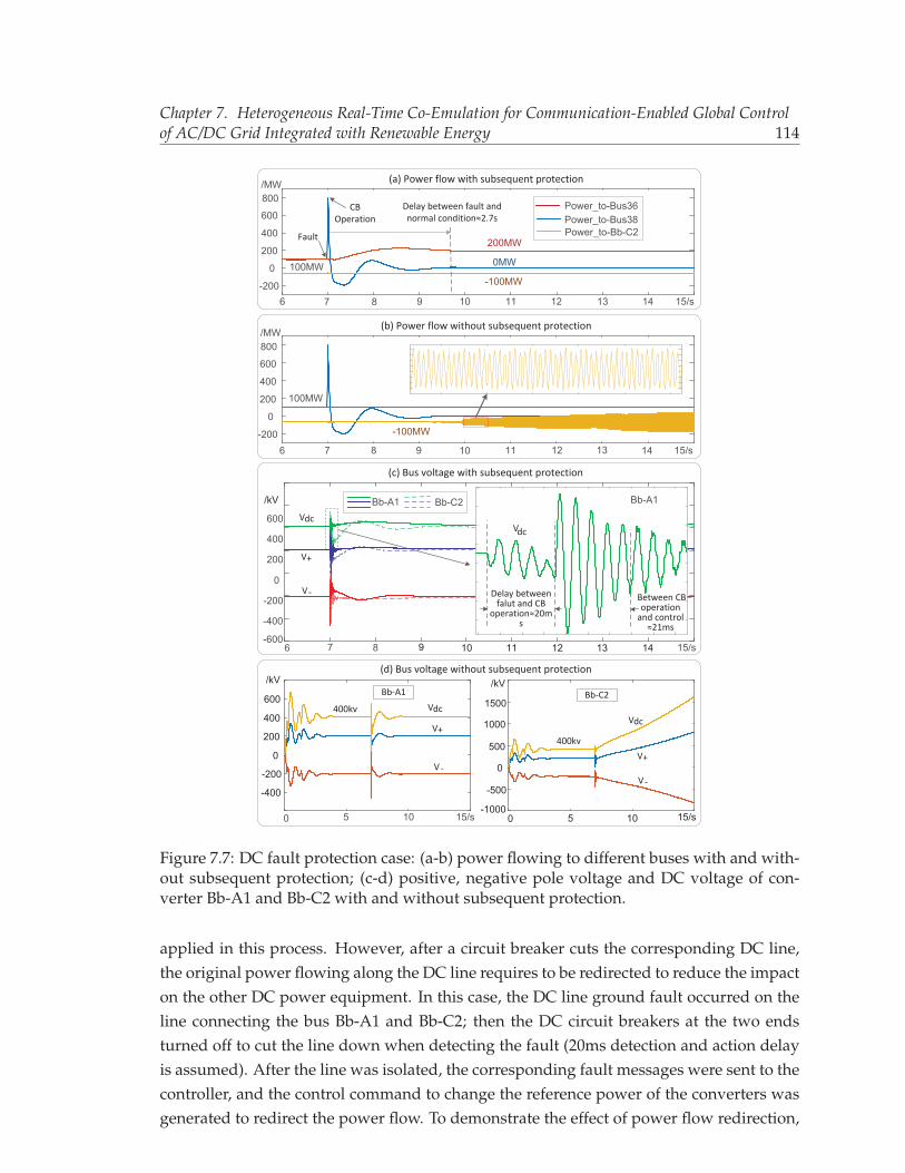
Chapter 7. Heterogeneous Real-Time Co-Emulation for Communication-Enabled Global Controlof AC/DC Grid Integrated with Renewable Energy 114
(a) Power flow with subsequent protection
(b) Power flow without subsequent protection
6 7 8 9 10 11 12 13 14 15/s
6 7 8 9 10 11 12 13 14 15/s-200
0
200
400
600
800
(d) Bus voltage without subsequent protection
(c) Bus voltage with subsequent protection
-200
0
200
400
600
800
0 5 10 15/s
/MW
/MW
0 5 10 15/s-1000
-500
0
500
1000
1500
/kV
V+
V-
Vdc
400kv
Bb-C2
6 7 8 15/s-600
-400
-200
0
200
400
600
/kV
9 10 11 12 13 14
Power_to-Bus36Power_to-Bus38Power_to-Bb-C2
100MW
200MW
0MW
-100MW
100MW
Bb-A1 Bb-C2
V+
V-
Vdc
-100MW
Vdc
Bb-A1
Delay between falut and CB
operation≈20ms
Delay between fault and normal condition≈2.7s
Between CB operation
and control ≈21ms
Fault
CBOperation
-400
-200
0
200
400
600
/kVBb-A1
400kv
V+
V-
Vdc
Figure 7.7: DC fault protection case: (a-b) power flowing to different buses with and with-out subsequent protection; (c-d) positive, negative pole voltage and DC voltage of con-verter Bb-A1 and Bb-C2 with and without subsequent protection.
applied in this process. However, after a circuit breaker cuts the corresponding DC line,the original power flowing along the DC line requires to be redirected to reduce the impacton the other DC power equipment. In this case, the DC line ground fault occurred on theline connecting the bus Bb-A1 and Bb-C2; then the DC circuit breakers at the two endsturned off to cut the line down when detecting the fault (20ms detection and action delayis assumed). After the line was isolated, the corresponding fault messages were sent to thecontroller, and the control command to change the reference power of the converters wasgenerated to redirect the power flow. To demonstrate the effect of power flow redirection,
Chapter 7. Heterogeneous Real-Time Co-Emulation for Communication-Enabled Global Controlof AC/DC Grid Integrated with Renewable Energy 115
the line between bus Bb-C2 and Bb-D1 was open at the beginning, and it was closed whenthe controller sent command to bus Bb-C2 and Bb-D1 after the DC fault.
The process was emulated on the hardware co-emulator and the results are presentedin Fig. 7.7. It can be observed from Fig. 7.7(a)(b) that with system-level control, the original100MW power flowing on the DC line between Bb-A1 and Bb-C2 was redirected to DC busBb-D1, and thus the power flowing to Bus36 increased to 200MW; although it took about2.7s to return to the normal condition. Without the system-level control, the extra powercould cause instability of the converter Cb-C2. From the DC voltages shown in Fig. 7.7(c),it can be seen that after the CB operation, there is a 21ms of transmission and controlcomputation delay before the control command took effect. The power redirection did notcause a big perturbation to the Vdc, which indicates the global control strategy is reasonableto reduce the system instability compared to purely cutting off the line without subsequentprotection operations.
7.6 Summary
To study the ICT-enabled global control for AC/DC grids integrated with renewable en-ergy, the co-simulation platform is required to evaluate the interaction between the powersystem and communication network. In this chapter, a heterogeneous hardware real-timeco-emulator is proposed and built on the multiple Jetson�-FPGA platform. The EMT-based power system simulation is executed on FPGA boards to provide a continuous mea-surement to the phasor measurement unit (PMU) and DC merging unit (DC-MU); theMMC converter control functions and communication modules run on the Jetson� em-bedded platform to perform fast and flexible computational tasks; and the interaction be-tween the two domains are simulated through the read and write operations via the PCIeconnector. The multi-board scheme is applied to extend the computational capabilities andresources to accommodate large-scale systems. The hybrid AC/DC grid with wind farmsis emulated on the FPGA-Jeston based co-emulator, and the ICT-enabled global controlschemes are investigated for the two case studies: power overflow and DC fault. The pro-posed heterogeneous co-emulator can be applied in fast emulation of practical large-scalecyber-physical power systems, and the investigated global control schemes can be appliedto improve the system stability and controllability.
8Conclusions and Future Work
With the development of AC power equipment, AC/DC power electronic converters, ICT-based smart meters, and controllable devices in modern power systems, fast and paral-lel hardware based simulation techniques are increasingly needed to deal with the large-scale complex power systems. The challenges in the EMT simulation area come from bothcomputational methods and implementation architectures: in the computation level, newpower equipment models are to be derived and applied for higher accuracy, and newcomputing methods are to be studied for faster matrix equation solutions; in the imple-mentation level, the advancements in the integrated circuit (IC) technology and computingscience should be leveraged to accommodate large systems and accelerate the simulationprocess.
In this thesis, three computational methods (multi-rate scheme, variable time-step-pingscheme and domain decomposition) and hardware (FPGA, MPSoC and GPU) based im-plementation architectures for fast and parallel power system EMT simulation are studiedand improved. For the multi-rate scheme, an extended multi-rate mixed-solver (MRMS)hardware architecture is first proposed for real-time EMT simulation of hybrid AC/DCnetworks. For the variable time-stepping scheme, the new mathematical computationalprocesses of the universal line model (ULM) and universal machine (UM) model are pro-posed to improve the stability. For the domain decomposition, a novel linking-domain ex-traction (LDE) decomposition method is proposed to solve the matrix equation in parallel.The hierarchical LDE method is further proposed to fully improve the LDE method. Forthe hardware based co-simulation architecture, the novel real-time co-emulation frame-works of the EMT-based power system and communication networks are proposed andconducted on the FPGA-MPSoC platform and Jetson�-FPGA platform respectively to ac-celerate the co-simulation for cyber-physical power systems.
116

Chapter 8. Conclusions and Future Work 117
The proposed computational methods and implementation architectures can be ap-plied in different aspects of the current EMT simulation research, and also benefit thedevelopment of the software or hardware based simulation tools. However, more workis required to be conducted in the future to follow the path of the completed works andextend the corresponding research. The specific and detailed contributions of this thesis,corresponding applications, and the directions of future work are described in this chapter.
8.1 Contributions of This Thesis
The main contributions of this thesis are summarized as follows:
• Computation-Level Contributions(1) Variable Time-Stepping Universal Line and Machine Models. The proposed “process-reverse” computational procedure and equivalent circuit for the ULM model andexciter of UM model can perform a stable computation no matter how the time-stepchanges, which greatly improve the stability of the traditional ULM and UM modelsfor VTS simulation.
(2) Linking-Domain Extraction (LDE) Based Domain Decomposition Method. The pro-posed LDE method can find the general formula of the matrix inversion to computethe matrix inverse in parallel, which is a new mathematical approach. The LDEmethod can not only be used in computing matrix inversion in parallel, but can alsoused in solving matrix equations after decomposing the system into subsystems.
(3) Hierarchical LDE (H-LDE) Decomposition Method. The proposed H-LDE methodeliminates the necessity of computing the entire conductance matrix and can fur-ther decompose the decomposed subsystems into sub-subsystems to accelerate theprocess of inverting the decomposed block matrices, which can achieve much lowerstorage costs and computation latencies than the original LDE method.
• Implementation-Level Contributions(1) Real-Time Multi-Rate Mixed-Solver Emulation Architecture on FPGA-MPSoC Plat-form. The multi-rate mixed-solver emulation architecture is proposed to simulatethe AC/DC power systems in real-time. By integrating the ARM� based processorsystem and FPGA based parallel computing, the proposed emulation architecturecan combine AC and DC power systems simulation together with hybrid linear andnonlinear solvers.
(2) Faster-than-Real-Time Emulation Architecture on FPGA and 4-Level Parallel SimulationArchitecture on GPU for VTS Simulation. The FPGA-based and GPU-based parallelsimulation architectures are proposed for VTS simulation. Through elaborate con-figuration to the time-step sizes of different subsystems, the “faster-than-real-time”
Chapter 8. Conclusions and Future Work 118
mode is achieved on FPGA; using the dynamic parallelism features and hierarchicaldecomposition, the massively parallel VTS simulation is achieved on GPU.
(3) Co-Emulation Hardware Architecture for Cyber-Physical Systems. The proposed real-time co-emulation (RTCE) framework is the first FPGA/MPSoC based emulation ar-chitecture to accelerate the co-emulation process of the EMT based power system andcommunication networks. The Jetson�-FPGA based heterogeneous co-emulationplatform is also proposed to practically study the communication enabled globalcontrol of hybrid AC/DC grids.
8.2 Applications of the Proposed Works
This section describes the potential applications of the proposed computation and imple-mentation techniques:
• The proposed multi-rate mixed-solver emulation architecture can be applied in theEMT simulation of large-scale AC/DC networks: the system decomposition andtime-step coordination, the multi-board solution, and collaboration between soft-processors and programmable logics can be utilized in various FPGA and embeddedarchitectures.
• The proposed VTS based universal line and machine models can be applied in theVTS power system simulation combining with other existing power equipment mod-els. The proposed “faster-than-real-time” simulation architecture on FPGA and 4-level hierarchically parallel simulation architecture on GPU can be applied in differ-ent platforms to conduct fast VTS-based EMT simulation.
• The proposed linking-domain decomposition method is a matrix-based decomposi-tion method, which can be applied in cases where the latency-based decompositionmethods cannot be used. The (hierarchical) LDE method can also be applied in tran-sient stability or power flow simulation within a certain power system scale.
• The proposed real-time co-emulation framework can be applied in emulating themodern cyber-physical power systems on programmable hardware platforms suchas FPGA and MPSoC, or the heterogeneous platforms such as the Jetson�-FPGAplatform, which can benefit the design, planning, and testing of the system levelcontrol schemes or new communication techniques in cyber-physical power systems.
8.3 Directions for Future Work
The following topics are proposed for future work:
Chapter 8. Conclusions and Future Work 119
• In the multi-rate simulation, different subsystems use different time-step sizes. Howto decompose a given power system into different subsystems automatically andhow to determine proper time-step sizes for the decomposed subsystems to guaran-tee reasonable accuracies remain to be investigated for the complete application ofthe multi-rate scheme.
• Similar to the automatic time-step configuration for multi-rate simulation, the vari-able time-stepping simulation also faces the problem of assigning proper time-stepsizes during the hardware based simulation. Although the LTE-based time-step con-trol schemes have been studied, how to determine the candidate time-step set priorto the simulation remains to be investigated.
• The automation problems also exit in the proposed LDE/H-LDE method. Althoughthere are already some topology partition algorithms available, they require to beintegrated with the LDE computation procedure. Besides, when the LDE decompo-sition comes to multi-levels, finding the automatic multi-level partition is requiredto make the H-LDE method really usable to users.
• The LDE method not only can be used in EMT simulation, but can also be used in thetransient stability and power flow simulation, which is the future application work.Besides, the application of the LDE method in finite element based power equipmentsimulation also needs to be further exploited.
• Since the proposed real-time co-emulators for the power system and communicationnetwork are implemented on hardware, the configuration for a test power system isnot as flexible as the software-based co-simulators, thus more programming effortneeds to be invested to provide an interface similar to what users use in practice.
• The conventional centralized power system structure is transforming into a moredistributed and autonomous pattern, which proposes new scenarios and challengesin co-simulating the cyber-physical systems such as ICT-enhanced microgrids andpower distribution systems. The corresponding co-simulation architectures requireto be designed and implemented.
Bibliography
[1] G. G. Parma and V. Dinavahi, “Real-time digital hardware simulation of power elec-tronics and drives,” IEEE Trans. Power Del., vol. 22, no. 2, pp. 1235-1246, Apr. 2007.
[2] B. Lu, X. Wu, H. Figueroa and A. Monti, “A low-cost real-time hardware-in-the-looptesting approach of power electronics controls,” IEEE Trans. Ind. Electron., vol. 54, no. 2,pp. 919-931, Apr. 2007.
[3] M. O. Faruque and V. Dinavahi, “Hardware-in-the-loop simulation of power electronicsystems using adaptive discretization,” IEEE Trans. Ind. Electron., vol. 57, no. 4, pp. 1146-1158, Apr. 2010.
[4] S. U. Grabic, et al., “Ultralow latency HIL platform for rapid development of complexpower electronics systems,” IEEE Trans. Power Electron., vol. 27, no. 11, pp. 4436-4444,Nov. 2012.
[5] F. N. Najm. Circuit Simulation. USA, Hoboken: John Wiley & Sons, 2010.
[6] K. Mets, J. A. Ojea, and C. Develder, “Combining power and communication networksimulation for cost-effective smart grid analysis,” IEEE Commun. Surveys Tuts., vol. 16,no. 3, pp. 1771-1796, 2014.
[7] B. Wu, High-Power Converters and AC Drives. Hoboken, NJ, USA: John Wiley & Sons,2006, pp. 3-13.
[8] Y. Chen and V. Dinavahi, “An iterative real-time nonlinear electromagnetic transientsolver on FPGA,” IEEE Trans. Ind. Electron., vol. 58, no. 6, pp. 2547-2555, Jun. 2011.
[9] Y. Chen and V. Dinavahi, “Multi-FPGA digital hardware design for detailed large-scalereal-time electromagnetic transient simulation of power systems,” IET Gener. Transm.Distrib., vol. 7, no. 5, pp. 451-463, May 2013.
[10] C. Deml and P. Turkes, “Fast simulation technique for power electronic circuits withwidely different time constants,” IEEE Trans. Ind. Appl., vol. 35, no. 3, pp. 657-662, May.1999.
[11] J. J. Sanchez-Gasca et al., “Extended-term dynamic simulation using variable timestep integration,” IEEE Comput. Appl. Power, vol. 6, no. 4, pp. 23-28, Oct. 1993.
120
Bibliography 121
[12] EMTDC� User’s Guide: A Comprehensive Resource for EMTDC, Version 4.7, ManitobaHVDC Research Centre, Winnipeg, Manitoba, Canada, 2010.
[13] Alternative Transient Program (ATP), http://www.emtp.org
[14] EMTP Alliance�, http://emtp-software.com/Overview
[15] PSpice� User’s Guide, Cadence Design Systems, Inc., 2000
[16] HSPICE� User Guide: Simulation and Analysis, Version B-2008.09, Synopsys, Inc.,2008
[17] Saber� User Guide, Version V-2004.06-SP1. Synopsys, Inc., 2004
[18] S. Hui, K. Fung, M. Zhang and C. Christopoulos, “Variable time step technique fortransmission line modeling,” IEE Proceedings A - Science, Measurement and Technology,vol. 140, no. 4, pp. 299-302, Jul. 1993.
[19] J. J. Sanchez-Gasca, R. D’Aquila, W. W. Price and J. J. Paserba, “Variable time step,implicit integration for extended-term power system dynamic simulation,” Proc. IEEEPower Ind. Comput. Appl. Conf., Salt Lake City, USA, pp. 183-189, May 1995.
[20] S. Henschel, A. I. Ibrahim and H. W. Dommel, “Transmission line model for vari-able step size simulation algorithms,” International Journal of Electrical Power & EnergySystems, vol. 21, no. 3, pp. 191-198, Mar. 1999.
[21] A. Ramirez and R. Iravani, “Frequency-domain simulation of electromagnetic tran-sients using variable sampling time-step,” IEEE Trans. Power Del., vol. 30, no. 6, pp.2602-2604, Dec. 2015.
[22] F. Camara, A. C. S. Lima and K. Strunz, “Full-frequency dependent models for vari-able time-step simulations,” CIGRE Session Papers & Proceedings, no. C4-302, pp. 1-11,2018.
[23] N. Lin and V. Dinavahi, “Variable time-stepping modular multi-level converter modelfor fast and parallel transient simulation of multi-terminal DC grid,” IEEE Trans. Ind.Electron., vol. 66, no. 9, pp. 6661-6670, Sept. 2019.
[24] Z. Shen and V. Dinavahi, “Dynamic variable time-stepping schemes for real-timeFPGA-based nonlinear electromagnetic transient emulation,” IEEE Trans. Ind. Electron.,vol. 64, no. 5, pp. 4006-4016, Jan. 2017.
[25] F. N. Najm, Circuit Simulation. USA, Hoboken: John Wiley & Sons, pp. 241-252, 2010.
[26] A. Morched, B. Gustavsen and M. Tartibi, “A universal model for accurate calculationof electromagnetic transients on overhead lines and underground cables,” IEEE Trans.Power Del., vol. 14, no. 3, pp. 1032-1038, Jul. 1999.
Bibliography 122
[27] H. K. Lauw and W. Scott Meyer, “Universal machine modeling for the representationof rotating electric machinery in an electromagnetic transients program,” IEEE Trans.Power Appl. Syst., vol. 101, no. 6, pp. 1342-1351, Jun. 1982.
[28] T. F. Chan and T. P. Mathew. Domain decomposition algorithms. Cambridge UniversityPress, 1994.
[29] A. Toselli and O.B. Widlund. Domain decomposition methods: algorithms and theory.Springer-Verlag Berlin Heidelberg, 2005.
[30] S. Y. R. Hui, K. K. Fung, and C. Christopoulos, “Decoupled simulation of multi-stage power electronic systems using transmission-line links,” in Proc. Rec. IEEE PowerElectron. Specialists Conf., Toledo, Spain, 1992, pp. 1324-1330.
[31] S. Y. R. Hui and K. K. Fung, “Fast decoupled simulation of large power electronicsystems using new two-port companion link models,” IEEE Trans. Power Electron., vol.12, no. 3, pp. 462-473, May 1997.
[32] J. E. Schutt-Aine, “Latency insertion method (LIM) for the fast transient simulationof large networks,” IEEE Trans. Circuits Syst. I: Fundam. Theory Appl., vol. 48, no. 1, pp.81-89, Jan. 2001.
[33] S. N. Lalgudi, M. Swaminathan, and Y. Kretchmer, “On-chip power-grid simulationusing latency insertion method,” IEEE Trans. Circuits Syst. I, vol. 55, no. 3, pp. 914-931,Apr. 2008.
[34] P. Aristidou, D. Fabozzi and T.V. Cutsem, “Dynamic simulation of large-scale powersystems using a parallel Schur complement-based decomposition method,” IEEE Trans.Parallel Distrib. Syst., vol. 25, no. 10, pp. 2561-2570, Oct. 2014.
[35] P. Aristidou, S. Lebeau and T.V. Cutsem, “Power system dynamic simulations usinga parallel two-level Schur complement decomposition,” IEEE Trans. Power Syst., vol. 31,no. 5, pp. 3984-3995, Sept. 2016.
[36] M. Baran, R. Sreenath, and N. Mahajan, “Extending EMTP for simulating agent baseddistributed applications,” IEEE Power Eng. Rev., pp. 52-54, Dec. 2002.
[37] J. Bergmann, C. Glomb, J. Goandtz, J. Heuer, R. Kuntschke, and M. Winter, “Scala-bility of smart grid protocols: Protocols and their simulative evaluation for massivelydistributed DERs,” in Proc. 1st IEEE Int. Conf. Smart Grid Commun. 2010 (SmartGrid-Comm’10), Oct. 2010, pp. 131-136.
[38] T. Godfrey, S. Mullen, R. C. Dugan, C. Rodine, D. W. Griffith, and N. Golmie, “Mod-eling smart grid applications with co-simulation,” in Proc. 1st IEEE Int. Conf. on SmartGrid Commun. 2010 (SmartGrid-Comm’10), 2010.

Bibliography 123
[39] V. Liberatore and A. Al-Hammouri, “Smart grid communication and co-simulation,”in Proc. IEEE Energytech 2011, may 2011, pp. 1-5.
[40] K. Hopkinson, X. Wang, R. Giovanini, J. Thorp, K. Birman, and D. Coury, “EPOCHS:a platform for agent-based electric power and communication simulation built fromcommercial off-the-shelf components,” IEEE Trans. Power Syst., vol. 21, no. 2, pp. 548-558, May 2006.
[41] H. Lin, S. Veda, S. Shukla, L. Mili, and J. Thorp, “GECO: Global event-drivenco-simulation framework for interconnected power system and communication net-works,” IEEE Trans. Smart Grid, vol. 3, no. 3, pp. 1444-1456, Sep. 2012.
[42] H. Georg, S. C. Muller, C. Rehtanz, and C. Wietfeld, “Analyzing cyberphysical energysystems: The INSPIRE co-simulation of power and ICT systems using HLA,” IEEETrans. Ind. Informat., vol. 10, no. 4, pp. 2364-2373, Nov. 2014.
[43] S. C. Muller, et al., “Interfacing power system and ICT simulators: challenges, state-of-the-art, and case studies,” IEEE Trans. Smart Grid, vol. 9, no. 1, pp. 14-24, Jan. 2018.
[44] V. Jalili-Marandi, Z. Zhou and V. Dinavahi, “Large-scale transient stability simulationof electrical power systems on parallel GPUs,” IEEE Trans. Parallel Distrib. Syst., vol. 23,no. 7, pp. 1255-1266, July 2012.
[45] Z. Zhou and V. Dinavahi, “Parallel massive-thread electromagnetic transient simula-tion on GPU,” IEEE Trans. Power Del., vol. 29, no. 3, pp. 1045-1053, June 2014.
[46] Z. Zhou and V. Dinavahi, “Fine-grained network decomposition for massively par-allel electromagnetic transient simulation of large power systems,” IEEE Power EnergyTechnol. Syst. J., vol. 4, no. 3, pp. 54-64, Sept., 2014.
[47] S. Yan, Z. Y. Zhou and V. Dinavahi, “Large-scale nonlinear device-level power elec-tronic circuit simulation on massively parallel graphics processing architectures,” IEEETrans. Power Electron., vol. 33, no. 6, pp. 4660-4678, June 2018.
[48] Y. Chen and V. Dinavahi, “FPGA-based real-time EMTP,” IEEE Trans. Power Del., vol.24, no. 2, pp. 892-902, Apr. 2009.
[49] Z. Shen and V. Dinavahi, “Design and implementation of real-time Mpsoc-FPGA-based electromagnetic transient emulator of CIGRE DC grid for HIL application,” IEEEPower Energy Technol. Syst. J., vol. 5, no. 3, pp. 104-116, Sept. 2018.
[50] T. Duan, Z. Shen and V. Dinavahi, “Multi-rate mixed-solver for real-time nonlinearelectromagnetic transient emulation of AC/DC networks on FPGA-MPSoC architec-ture,” IEEE Power Energy Technol. Syst. J., vol. 6, no. 4, pp. 183-194, Dec. 2019.
Bibliography 124
[51] NVIDIA Corporation, Dynamic parallelism in Cuda, downloaded in June 2018.
[52] VCU118 Evaluation Board User Guide (UG1224), Xilinx Inc., San Jose, CA, USA, Oct.2018.
[53] Vivado Design Suite User Guide, High-Level Synthesis, UG902 (v2015.1). Xilinx, Inc.,2015
[54] ZCU102 Evaluation Board User Guide (UG1182), Xilinx Inc., San Jose, CA, USA, Oct.2018.
[55] L. O. Chua, “Efficient computer algorithms for piecewise linear analysis of resistivenonlinear networks,” IEEE Trans. Circuit Theory, vol. 18, no. 1, pp. 73-85, Jan. 1971.
[56] H. W. Dommel, “Nonlinear and time-varying elements in digital simulation of elec-tromagnetic transients,” IEEE Trans. Power App. Syst., vol. 90, no. 6, pp. 2561-2567, Nov.1971.
[57] PSCADTM IEEE 39 Bus System, Revision 1, Manitoba HVDC Research Centre, Win-nipeg, Manitoba, Canada, 2010.
[58] Aurora 64B/66B LogiCORE IP Product Guide, PG074 (V11.2), Xilinx Inc., San Jose, CA,USA, Apr. 2018.
[59] Protection Against Lightning Electromagnetic Impulse - Part I : General Principles,IEC Standard 1312-I, Feb. 1995.
[60] N. R. Tavana and V. Dinavahi, “Real-time nonlinear magnetic equivalent circuitmodel of induction machine on FPGA for hardware-in-the-loop simulation,” IEEETrans. Energy Convers., vol. 31, no. 2, pp. 520-530, June 2016.
[61] J. Liu and V. Dinavahi, “Detailed magnetic equivalent circuit based real-time non-linear power transformer model on FPGA for electromagnetic transient studies,” IEEETrans. Ind. Electron., vol. 63, no. 2, pp. 1191-1202, Feb. 2016.
[62] W. Wang, Z. Shen and V. Dinavahi, “Physics-based device-level power electroniccircuit hardware emulation on FPGA,” IEEE Trans. Ind. Informat., vol. 10, no. 4, pp.2166-2179, Nov. 2014.
[63] N. Lin and V. Dinavahi, “Dynamic electro-magnetic-thermal modeling of MMC-based DC-DC converter for real-time simulation of MTDC grid,” IEEE Trans. PowerDel., vol. 33, no. 3, pp. 1337-1347, June 2018.
[64] B. Gustavsen, G. Irwin, R. Mangelrod, D. Brandt and K. Kent, “Transmission linemodels for the simulation of interaction phenomena between parallel AC and DC over-head lines,” IPST’99 International Conference on Power Systems Transients, Budapest Hun-gary, pp. 61-68, Jun. 1999.
Bibliography 125
[65] B. Gustavsen and A. Semlyen, “Simulation of transmission line transients using vec-tor fitting and modal decomposition,” IEEE Trans. Power Del., vol. 13, no. 2, pp. 605-614,Apr. 1998.
[66] Y. Chen and V. Dinavahi, “Digital hardware emulation of universal machine anduniversal line models for real-time electromagnetic transient simulation,” IEEE Trans.Ind. Electron., vol. 59, no. 2, pp. 1300-1309, Feb. 2012.
[67] L. Wang and J. Jatskevich, “A voltage-behind-reactance synchronous machine modelfor the EMTP-type solution,” IEEE Trans. Power Syst., vol. 21, no. 4, pp. 1539-1549, Nov.2006.
[68] J. Liu and V. Dinavahi, “A real-time nonlinear hysteretic power transformer transientmodel on FPGA,” IEEE Trans. Ind. Electron., vol. 61, no. 7, pp. 3587-3597, Jul. 2014.
[69] PSCADTM IEEE 118 Bus System, Revision 1, Manitoba HVDC Research Centre, Win-nipeg, Manitoba, Canada, 2010.
[70] M. A. Woodbury. Inverting modified matrices. Memorandum Rept. 42, Statistical Re-search Group, Princeton University, Princeton, NJ, 1950.
[71] Y. Chen and V. Dinavahi, “Multi-FPGA digital hardware design for detailed large-scale real-time electromagnetic transient simulation of power systems,” IET Gener.Transm. Distrib., vol. 7, no. 5, pp. 451-463, May 2013.
[72] Y. Chen and V. Dinavahi, “Hardware emulation building blocks for real-time simu-lation of large-scale power grids,” IEEE Trans. Ind. Informat., vol. 10, no. 1, pp. 373-381,Feb. 2014.
[73] Z. Shen and V. Dinavahi, “Real-time device-level transient electrothermal model formodular multilevel converter on FPGA,” IEEE Trans. Power Electron., vol. 31, no. 9, pp.6155-6168, Sept. 2016.
[74] Z. Huang and V. Dinavahi, “A fast and stable method for modeling generalizednonlinearities in power electronic circuit simulation and its real-time implementation,”IEEE Trans. Power Electron., vol. 34, no. 4, pp. 3124-3138, Apr. 2019.
[75] N. Lin and V. Dinavahi, “Detailed device-level electrothermal modeling of the proac-tive hybrid HVDC breaker for real-time hardware-in-the-loop simulation of DC grids,”IEEE Trans. Power Electron., vol. 33, no. 2, pp. 1118-1134, Feb. 2018.
[76] J. J. Grainger, W. D. Stevenson, Power System Analysis. McGraw Hill Inc., 1994.
[77] K. Sun, Q. Zhou, K. Mohanram and D. C. Sorensen, “Parallel domain decompositionfor simulation of large-scale power grids,” 2007 IEEE/ACM International Conference onComputer-Aided Design, no. 9789742, San Jose, CA, USA, Nov. 2007
Bibliography 126
[78] T. Duan and V. Dinavahi, “A novel linking-domain extraction decomposition methodfor parallel electromagnetic transient simulation of large-scale AC/DC networks,” IEEETrans. Power Del., early-access, May 2020.
[79] T. A. Davis, and E. P. Natarajan, “Algorithm 907: KLU, a direct sparse solver for circuitsimulation problems,” ACM Trans. Mathematical Software, vol. 37, no. 6, pp. 36:1-36:17,2010.
[80] X. Chen, Y. Wang, and H. Yang, “NICSLU: an adaptive sparse matrix solver for par-allel circuit simulation,” IEEE Trans. Comput.-Aided Design Integr. Circuits Syst., vol. 32,no. 2, pp. 261-274, Feb 2013.
[81] EECS Department of the University of California at Berke-ley, “SPICE: Simulation Program with Integrated Circuit Emphasis,”http://bwrcs.eecs.berkeley.edu/Classes/IcBook/SPICE/
[82] NVIDIA Tesla V100 Datasheet. Dec. 2017. [Online]. Available:http://www.nvidia.com/content/PDF/Volta-Datasheet.pdf
[83] S. Peyghami, P. Davari, M. Fotuhi-Firuzabad, and F. Blaabjerg, “Standard test systemsfor modern power system analysis: an overview,” IEEE Ind. Electron. Mag., vol. 13, no.4, pp. 86-105, Dec. 2019.
[84] Y. Cao, X. Shi, Y. Li, Y. Tan, M. Shahidehpour and S. Shi, “A simplified co-simulationmodel for investigating impacts of cyber-contingency on power system operations,”IEEE Tran. Smart Grid, vol. 9, no. 5, pp. 4893-4905, Sept. 2018.
[85] A. A. Jahromi, A. Kemmeugne, D. Kundur and A. Haddadi, “Cyber-physical attackstargeting communication-assisted protection schemes,” IEEE Tran. Power Syst., vol. 35,no. 1, pp. 440-450, Jan. 2020.
[86] Q. Wang, W. Tai, Y. Tang, Y. Liang, L. Huang and D. Wang, “Architecture and applica-tion of real-time co-simulation platform for cyber-physical power system,” in Proc. 7thIEEE Int. Conf. Cyber Technol. in Autom., Control and Intell. Syst., Hawaii, USA, pp. 81-85,July 31-August 4, 2017.
[87] G. Cao, W. Gu, C. Gu, W. Sheng, J. Pan, R. Li and L. Sun, “Real-time cyber-physicalsystem co-simulation testbed for microgrids control,” IET Cyber-Phys. Syst., Theory Appl.,Vol. 4, Iss. 1, pp. 38-45, Feb. 2019.
[88] B. Chen, K. L. Butler-Purry, A. Goulart and D. Kundur, “Implementing a real-timecyber-physical system test bed in RTDS and OPNET,” 2014 North American Power Sym-posium (NAPS), Pullman, USA, pp. 1-6, Sept. 2014.
Bibliography 127
[89] H. Tong, M. Ni, L. Zhao and M. Li, “Flexible hardware-in-the-loop testbed for cyberphysical power system simulation,” IET Cyber-Phys. Syst., Theory Appl., Vol. 4, Iss. 4, pp.374-381, Aug. 2019.
[90] “IEEE Standard for Synchrophasor Measurements for Power Systems,” IEEE StdC37.118.1, IEEE Power & Energy Society, New York, NY, 2011.
[91] J. Bergmann, C. Glomb, J. Goandtz, J. Heuer, R. Kuntschke, and M. Winter, “Scala-bility of smart grid protocols: Protocols and their simulative evaluation for massivelydistributed DERs,” in Proc. 1st IEEE Int. Conf. Smart Grid Commun. 2010 (SmartGrid-Comm’10), Oct. 2010, pp. 131-136.
[92] V. Liberatore and A. Al-Hammouri, “Smart grid communication and co-simulation,”in Proc. IEEE Energytech 2011, may 2011, pp. 1-5.
[93] T. Godfrey, S. Mullen, R. C. Dugan, C. Rodine, D. W. Griffith, and N. Golmie, “Mod-eling smart grid applications with co-simulation,” in Proc. 1st IEEE Int. Conf. on SmartGrid Commun. 2010 (SmartGrid-Comm’10), 2010.
[94] H. Lin, S. Sambamoorthy, S. Shukla, J. Thorp, and L. Mili, “Power system and com-munication network co-simulation for smart grid applications,” in Proc. IEEE/PES Inno-vative Smart Grid Technol. 2011 (ISGT’11), Jan. 2011, pp. 1-6.
[95] F. Aalamifar, A. Schlogl, D. Harris, and L. Lampe. “Modelling power line communi-cation using network simulator-3.” http://www.ece.ubc.ca/ faribaa/paper.pdf.
[96] J. Nutaro, “Designing power system simulators for the smart grid: combining con-trols, communications, and electro-mechanical dynamics,” in Proc. IEEE Power and En-ergy Society General Meeting 2011 (PES’11), 2011, pp. 1-5.
[97] K. Mets, T. Verschueren, C. Develder, T. L. Vandoor, and L. Vandevelde, “Integratedsimulation of power and communication networks for smart grid applications,” in Proc.IEEE 16th Int. Workshop Computer Aided Modeling and Design of Commun. Links and Net-works 2011 (CAMAD’11), Kyoto, Japan, 10-11, June 2011.
[98] R. Mora et al., “Demand management communications architecture,” in Proc. 20thInt. Conf. Electricity Distribution (CIRED’09), Prague, 2009, pp. 8-11.
[99] T. Sidhu and Y. Yin, “Modelling and simulation for performance evaluation ofIEC61850-based substation communication systems,” IEEE Trans. Power Del., vol. 22,no. 3, pp. 1482-1489, July 2007.
[100] W. Li, A. Monti, M. Luo, and R. Dougal, “VPNET: A co-simulation framework foranalyzing communication channel effects on power systems,” in Proc. IEEE Electric ShipTechnologies Symp. 2011 (ESTS’11), April 2011, pp. 143-149.
Bibliography 128
[101] K. Zhu, M. Chenine, and L. Nordstrom, “ICT architecture impact on wide areamonitoring and control systems’ reliability,” IEEE Trans. Power Del., vol. 26, no. 4, pp.2801-2808, Oct. 2011.
[102] E. Moradi-Pari, N. Nasiriani, Y. P. Fallah, P. Famouri, S. Bossart and K. Dodrill, “De-sign, modeling, and simulation of on-demand communication mechanisms for cyber-physical energy systems,” IEEE Trans. Ind. Informat., vol. 10, no. 4, pp. 2330-2339, Nov.2014.
[103] “Communication networks and systems for power utility automation - Part 1: In-troduction and overview,” IEC TR 61850-1:2013, 2013.
[104] “Communication networks and systems for power utility automation - Part 90-5:Use of IEC 61850 to transmit synchrophasor information according to IEEE C37.118,”IEC TR 61850-90-5, Jan. 2012.
[105] F. Aalamifar, A. Schlogl, D. Harris, and L. Lampe. “Modelling power line communi-cation using network simulator-3.” http://www.ece.ubc.ca/faribaa/paper.pdf.
[106] Xilinx Doc. XAPP1026 (v5.1), “LightWeight IP Application Examples,” Nov. 21,2014.
[107] R. Abe, H. Taoka, and D. McQuilkin, “Digital grid: communicative electrical gridsof the future,” IEEE Trans. Smart Grid, vol. 2, no. 2, pp. 399-410, June 2011.
[108] M. Davari, and Y. A. I. Mohamed, “Dynamics and robust control of a grid-connectedVSC in multiterminal DC grids considering the instantaneous power of DC- and AC-side filters and DC grid uncertainty,” IEEE Trans. Power Electron., vol. 31, no. 3, pp.1942-1958, Mar. 2016.
[109] X. Li, L. Guo, C. Hong, Y. Zhang, Y. W. Li, and C. Wang, “Hierarchical controlof multiterminal DC grids for large-scale renewable energy integration,” IEEE Trans.Sustain. Energy, vol. 9, no. 3, pp. 1448-1457, July 2018.
[110] S. Debnath, J. Qin, B. Bahrani,M. Saeedifard, and P. Barbosa, “Operation, control,and applications of the modular multilevel converter: A review,” IEEE Trans. PowerElectron., vol. 30, no. 1, pp. 37-53, Jan. 2015.
[111] X. Shi, B. Liu, Z. Wang, Y. Li, L. M. Tolbert, and F. Wang, “Modeling, control design,and analysis of a startup scheme for modular multilevel converters,” IEEE Trans. Ind.Electron., vol. 62, no. 11, pp. 7009-7024, Nov. 2015.
[112] P. Wang, C. Jin, D. Zhu, Y. Tang, P. C. Loh, and F. H. Choo, “Distributed control forautonomous operation of a three-port AC/DC/DS hybrid microgrid,” IEEE Trans. Ind.Electron., vol. 62, no. 2, pp. 1279-1290, Feb.. 2015.
Bibliography 129
[113] C. Qi, K. Wang, Y. Fu, G. Li, B. Han, R. Huang, and T. Pu, “A decentralized optimaloperation of AC/DC hybrid distribution grids,” IEEE Trans. Smart Grid, vol. 9, no. 6,pp. 6095-6105, Nov. 2018.
[114] L. Zhang, Y. Tang, S. Yang, and F. Gao, “Decoupled power control for a modular-multilevel-converter-based hybrid AC–DC grid integrated with hybrid energy storage,”IEEE Trans. Ind. Electron., vol. 66, no. 4, pp. 2926-2934, April 2019.
[115] J. Zhai, et al., “Hierarchical and robust scheduling approach for VSC-MTDC meshedAC/DC grid with high share of wind power,” IEEE Trans. Power Syst., early-access, pp.1-12, July 2020.
[116] NVIDIA�, “NVIDIA Jetson AGX Xavier developer kit: powering AI in autonomousmachines,” Data Sheet, Oct. 2018.
[117] S. Peyghami, P. Davari, M. Fotuhi-Firuzabad, and F. Blaabjerg, “Standard test sys-tems for modern power system analysis: an overview,” IEEE Ind. Electron. Mag., vol.13, no. 4, pp. 86-105, Dec. 2019.
[118] M. Adamiak, B. Kasztenny, and W. Premerlani, “Synchrophasors: definition, mea-surement, and application,” presented at the 59th Annu. Georgia Tech Protective Relaying,Atlanta, GA, Apr. 27-29, 2005.
[119] R. Burgos and J. Sun, “The future of control and communication: power electronics-enabled power grids,” IEEE Power Electron. Mag., vol. 7, no. 2, pp. 34-36, June 2020.
[120] Z. Shen, T. Duan and V. Dinavahi, “Design and implementation of real-time MPSoC-FPGA based electromagnetic transient emulator of CIGRE DC grid for HIL application,”IEEE Power Energy Technol. Syst. J., vol. 5, no. 3, pp. 104-116, Sept. 2018.
[121] PSCAD/EMTDC�, “CIGRE B4-57 working group developed models,” ExampleCase, available at: https://www.pscad.com/knowledge-base/article/57
[122] Z. Shen and V. Dinavahi, “Comprehensive electromagnetic transient simulation ofAC/DC grid with multiple converter topologies and hybrid modeling schemes,” IEEEPower Energy Technol. Syst. J., vol. 4, no. 3, pp. 40-50, Sept. 2017.
[123] G. Carrara, S. Gardella, M. Marchesoni, R. Salutari and G. Sciutto, “A new multilevelPWM method: a theoretical analysis,” IEEE Trans. Power Electron., vol. 7, no. 3, pp. 497-505, Jul. 1992.
[124] L. Liu, M. Popov, P. Palensky, and M. V. D. Meijden, “A fast protection of multi-terminal HVDC system based on transient signal detection,” IEEE Trans. Power Del.,early-access, pp. 1-9, 2020. DOI: 10.1109/TPWRD.2020.2979811.
Related Documents