EE225C Final Report Fall 2000 12/12/2000 OFDM Receiver Design Yun Chiu, Dejan Markovic, Haiyun Tang, Ning Zhang {chiuyun, dejan, tangh, ningzh}@eecs.berkeley.edu Abstract Othogonal Frequency Division Multiplex (OFDM) has gained considerable attention in recent years. It has been adopted for various standards include the 802.11a wireless LAN standard. In this project, we implemented an OFDM receiver based 802.11a standard. Furthermore, since spatial diversity is the ultimate way to increase system capacity in bandwidth-cautious wireless applications, the SVD antenna-array processing algorithm is also implemented and will be integrated with the OFDM receiver. Key system blocks including Cordic, FFT, Viterbi decoder, and SVD are implemented in both Simulink and Module Compiler. Simulink simulation of the OFDM receiver is performed and BER is determined. Total chip area of the OFDM system in 0.25mm process is 430mm 2 and dissipates about 2.6W of power, dominated by the SVD array.

Ofdm Receiver Design
Oct 24, 2015
OFDM Receiver Design
Welcome message from author
This document is posted to help you gain knowledge. Please leave a comment to let me know what you think about it! Share it to your friends and learn new things together.
Transcript
EE225C Final Report Fall 2000 12/12/2000
OFDM Receiver Design
Yun Chiu, Dejan Markovic, Haiyun Tang, Ning Zhang
{chiuyun, dejan, tangh, ningzh}@eecs.berkeley.edu
Abstract Othogonal Frequency Division Multiplex (OFDM) has gained considerable attention in recent years. It has been adopted for various standards include the 802.11a wireless LAN standard. In this project, we implemented an OFDM receiver based 802.11a standard. Furthermore, since spatial diversity is the ultimate way to increase system capacity in bandwidth-cautious wireless applications, the SVD antenna-array processing algorithm is also implemented and will be integrated with the OFDM receiver. Key system blocks including Cordic, FFT, Viterbi decoder, and SVD are implemented in both Simulink and Module Compiler. Simulink simulation of the OFDM receiver is performed and BER is determined. Total chip area of the OFDM system in 0.25mm process is 430mm2 and dissipates about 2.6W of power, dominated by the SVD array.
1. Overview
1.1 Background Orthogonal Frequency Division Multiplex (OFDM) system has inherent advantage over single carrier system in frequency-selective fading channel. It has been adopted by various standards in recent years including DSL and 802.11a wireless LAN standards.
1.2 Project goal The goal of the project is to: 1. Implement an OFDM digital receiver that conforms to the 802.11a standard 2. Integrate antenna-array processing module into the OFDM system.
The antenna-array processing module implements the SVD algorithm proposed in the TFS radio project.
1.3 Report organization The report is organized into six sections. The second section discusses the basics of OFDM and various practical problems with OFDM. The system architecture of 802.11a is introduced in the third section. The synchronization and channel estimation schemes are discussed. Section four discusses the system Simulink simulation including the detailed implementation of individual blocks. Section five talks about the VHDL implementation of several key blocks of the OFDM receiver as well as the testing and simulation results for these blocks. The reported is concluded by section six.
2. Introduction to OFDM
2.1 Signal representation In an OFDM system, data is carried on narrow-band sub-carriers in frequency domain. Data was
transformed into time-domain using IFFT at the transmitter and transformed back to frequency-domain using FFT at the receiver. The total number of sub-carriers translates into the number of points of the IFFT/FFT.
Suppose the data set to be transmitted is )12/(,),12/(),2/( −+−− NUNUNU K
where N is the total number of sub-carriers. The discrete-time representation of the signal after IFFT is
∑−
−=
π=
12/
2/
2)(
1)(
N
Nk
nNk
jekU
Nnu
where )2/,2/[ NNn −∈ . At the receiver side, the data is recovered by performing FFT on the received signal, i.e.
∑−
−=
π−=
12/
2/
2)(
1)(
N
Nn
kNn
jenu
NkU
where )2/,2/[ NNk −∈ . Most literature uses the continuous-time representation of the signal, i.e.
∑−
−=
−π12/
2/
)2/(2)(
1 N
Nk
TtTk
jekU
N
where ),0[ Tt ∈ and T is the symbol period. The k-th datum )(kU is carried on the k-th narrowband carrier
tTk
je
π2
Notice that the samples of the continuous-time signal at
NTN
NT
NT )1(
,,2
,,0−
K
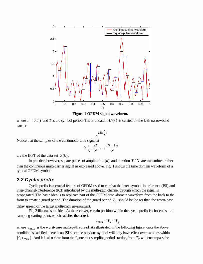
are the IFFT of the data set )(kU . In practice, however, square pulses of amplitude )(nu and duration NT / are transmitted rather
than the continuous multi-carrier signal as expressed above. Fig. 1 shows the time domain waveform of a typical OFDM symbol.
2.2 Cyclic prefix Cyclic prefix is a crucial feature of OFDM used to combat the inter-symbol-interference (ISI) and
inter-channel-interference (ICI) introduced by the multi-path channel through which the signal is propagated. The basic idea is to replicate part of the OFDM time-domain waveform from the back to the front to create a guard period. The duration of the guard period gT should be longer than the worst-case
delay spread of the target multi-path environment. Fig. 2 illustrates the idea. At the receiver, certain position within the cyclic prefix is chosen as the
sampling starting point, which satisfies the criteria gx TT <<τmax
where maxτ is the worst-case multi-path spread. As illustrated in the following figure, once the above condition is satisfied, there is no ISI since the previous symbol will only have effect over samples within
],0[ maxτ . And it is also clear from the figure that sampling period starting from xT will encompass the
0 0.1 0.2 0.3 0.4 0.5 0.6 0.7 0.8 0.9 10
0.5
1
1.5
2
2.5
3
t/T
Continuous-time waveformSquare-pulse waveform
Figure 1 OFDM signal waveform.
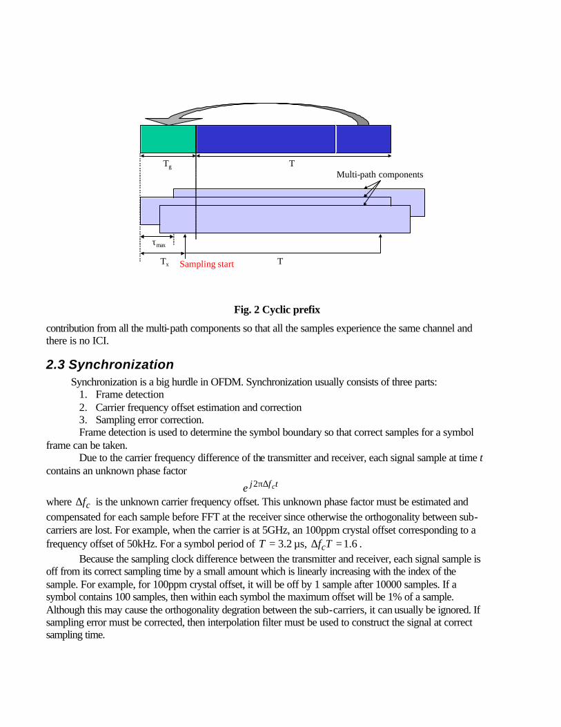
contribution from all the multi-path components so that all the samples experience the same channel and there is no ICI.
2.3 Synchronization Synchronization is a big hurdle in OFDM. Synchronization usually consists of three parts:
1. Frame detection 2. Carrier frequency offset estimation and correction 3. Sampling error correction. Frame detection is used to determine the symbol boundary so that correct samples for a symbol
frame can be taken. Due to the carrier frequency difference of the transmitter and receiver, each signal sample at time t
contains an unknown phase factor
where cf∆ is the unknown carrier frequency offset. This unknown phase factor must be estimated and compensated for each sample before FFT at the receiver since otherwise the orthogonality between sub-carriers are lost. For example, when the carrier is at 5GHz, an 100ppm crystal offset corresponding to a frequency offset of 50kHz. For a symbol period of 2.3=T µs, 6.1=∆ Tfc .
Because the sampling clock difference between the transmitter and receiver, each signal sample is off from its correct sampling time by a small amount which is linearly increasing with the index of the sample. For example, for 100ppm crystal offset, it will be off by 1 sample after 10000 samples. If a symbol contains 100 samples, then within each symbol the maximum offset will be 1% of a sample. Although this may cause the orthogonality degration between the sub-carriers, it can usually be ignored. If sampling error must be corrected, then interpolation filter must be used to construct the signal at correct sampling time.
Tg T
τmax
Tx
Multi-path components
TSampling start
Fig. 2 Cyclic prefix
tfj ce ∆π2
2.4 Channel estimation For burst communication system, training symbols are used at the beginning of each burst. Since the burst is short, the channel is assumed static over a whole burst so that once the channel is estimated, the inverse of the estimated channel response will be used to compensate the signal for the whole burst. Assuming the received signal after FFT is
)()()()( kZkXkCkY += where k is sub-carrier index, C is the channel, X is the pilot data, and Z is the noise. The simplest way to estimate the channel is then by
)()(
)(ˆkXkY
kC =
i.e. dividing the received signal by the known pilot. Without noise, this gives the correct estimation. When noise is present, there could be error.
3. System architecture
3.1 System parameters The following table shows the main system parameters of the 802.11a wireless LAN standard.
Sample rate 20MHz Chip duration 50ns Number of FFT points 64 Number of sub-carriers 52 Number of data sub-carriers 48 Number of pilot sub-carriers 4 OFDM symbol period 4µs (80 chips)
Cyclic prefix 0.8µs (16 chips)
FFT symbol period 3.2µs (64 chips) Modulation scheme BPSK, QPSK, 16QAM, 64QAM Coding ½ convolutional, constraint length 7, optional puncturing Data rate 6, 9, 12, 18, 24, 36, 48, 54 Mbps
The system is operating at a sampling rate of 20MHz. It uses 64-point FFT. The OFDM frame duration worths 80 chips where 64 is for data while 16 is cyclic prefix. This corresponds an efficiency of 4/5. Out of the 64 narrow-band sub-carriers, only 52 are carrying signal and other 12 are zeros. Four of the 52 sub-carriers are used as pilots and the other 48 are used for data. Using different modulation scheme combined with puncturing of the convolutional encoder, variable data rate can be achieved with a minimum of 6 Mbps and maximum of 54 Mbps.
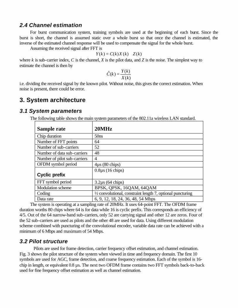
3.2 Pilot structure Pilots are used for frame detection, carrier frequency offset estimation, and channel estimation.
Fig. 3 shows the pilot structure of the system when viewed in time and frequency domain. The first 10 symbols are used for AGC, frame detection, and coarse frequency estimation. Each of the symbol is 16-chip in length, or equivalent 0.8 µs. The next two OFDM frame contains two FFT symbols back-to-back used for fine frequency offset estimation as well as channel estimation.
When viewed in frequency domain, the first 10 short symbols uses 12 sub-carriers each. Four out of the 52 carriers are used as pilot for correcting the residual frequency offset error which tends to accumulate over symbols.
3.3 Frame detection The first ten short symbols are the same and used for frame detection. The received signal is
correlated with the known short symbol waveform. The received signal also correlated with itself with a delay of one short symbol. The correlation with known symbol creates peaks. The self-correlation of the signal creates a plateau of the length of 10 short symbols. If the correlation peaks are within the plateau. The last peak is used as the beacon position from where the start of the next symbol is determined.
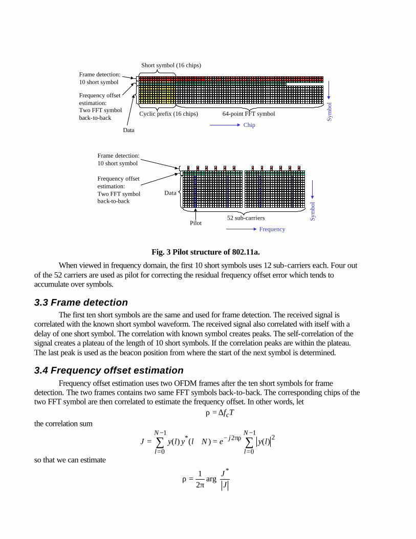
3.4 Frequency offset estimation Frequency offset estimation uses two OFDM frames after the ten short symbols for frame
detection. The two frames contains two same FFT symbols back-to-back. The corresponding chips of the two FFT symbol are then correlated to estimate the frequency offset. In other words, let
Tfc∆=ρ the correlation sum
∑∑−
=
πρ−−
==+=
1
0
221
0
* )()()(N
l
jN
llyeNlylyJ
so that we can estimate
π=ρ
JJ *
arg21
Cyclic prefix (16 chips)
Short symbol (16 chips)
64-point FFT symbol
Frame detection: 10 short symbol
Frequency offset estimation: Two FFT symbol back-to-back
DataChip
Sym
bol
52 sub-carriers
Frequency
Sym
bol
Frame detection: 10 short symbol
Frequency offset estimation: Two FFT symbol back-to-back
Data
Pilot
Fig. 3 Pilot structure of 802.11a.
In view of the possibility that ρ may be bigger than 1 (e.g. 1.6 at 100ppm crystal offset), a coarse estimation on ρ is performed using short symbols. Correlating adjacent short symbols, we have
∑∑−
=
πρ−−
==+=
14/
0
24/214/
0
* )()4/()(N
l
jN
llyeNlylyK
so that
π=
ρKK*
arg21
4
Since ρ/4 is less than 1 even at 100ppm, there is no ambiguity in determining the value of ρ. On the other hand, since it correlates only 1/4 of the total chips in a symbol the result is less accurate. Combining the above coarse and fine estimation, we arrive at the estimation
π+
π=ρ
JJ
KK **
arg21
24
where means truncating to integer towards zero.
3.5 Channel estimation Channel estimation uses the same two OFDM symbols as the frequency offset estimation. Once frame start is detected, frequency offset is estimated, and signal samples are compensated. They are transformed into frequency domain by FFT. For each sub-carrier, we have
)()()()( kZkXkCkY += and the channel C is estimated as
)()(
)(ˆkXkY
kC =
Conv.Encoder
IFFT CyclicPrefix
ViterbiDecoder FFT
ChannelEst. & Comp.
Synchroni-zation
Multi-pathChannel
Tx SVD
Rx SVD
OFDM
SVD Feedback Link
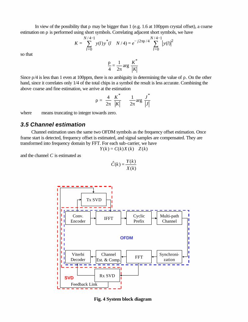
Fig. 4 System block diagram

4. System simulation The system simulation is implemented in Simulink. The system block diagram is shown in Fig. 4. In order to do system level simulation, a transmitter-channel-receiver chain is modeled in Matlab/ Simulink. Besides the fixed-point blocks we implemented, there are several blocks which we left out for hardware implementation, yet they are necessary to make the whole system together. These blocks are described below and they are modeled with floating-point.
4.1. Synchronization, Frequency Offset Compensation
Txer and rxer frequency offset is problematic in OFDM multi-carrier communication systems due to the close spacing between sub-carriers and therefore the high sensitivity to loss of orthogonality. Digital signal processing techniques are explored in this project study to implement efficient offset estimation and compensation schemes. Since the operation of these blocks exhibits a close relationship with the synchronization and frame timing circuits of the receiver, a joint design study of both modules for an IEEE 802.11a receiver is carried out. In this report, we will present a robust double correlation based frame synchronization algorithm. The worst case sync uncertainty of 8 chips (samples) is obtained, which directly corresponds to the max multi-path delay of the channel. This is well below the specified 16-chip cyclic prefix length, therefore results in no loss of performance after CP removal. A coarse-fine joint frequency estimation algorithm is also designed to enable a large freq offset of ±100ppm at 5.8GHz carrier freq to be detected. The simulated accuracy of the estimation module is ≤1% under 15dB SNR at the front-end of the rxer. A txer model that is fully compatible with the IEEE 802.11a standard is also written in SIMULINK to enable the system simulation of the full receiver.
Figure 4.1 Double correlation based frame synchronization scheme
4.1.2. Frame Start Synchronization
IEEE 802.11a specifies two preambles to use for frame synchronization, frequency offset estimation, and channel estimation. We exploit the short (16 chip) periodicity of the first preamble to derive the frame start signal as soon as the preamble ends. Correlation of the rxed sample to the known short preamble sequence is performed first. Due to the excellent auto-correlation peoperty of the preamble, it results in periodic strong peaks that enables the detection of the symbol boundary precisely. However, random data following the preamble may generate short correlation peaks that resemble the desired peaks. To improve the robustness of the algorithm, the auto-correlation of the rxed samples with a delayed copy of itself is also performed. Due to the periodic nature of the preamble, a 160 chip long plateau is produced which is unique to the preamble period. A joint decision of the frame sync is based on both of the correlation results. The long plateau rules out any short glitches following the real preamble. Multi-path channel response and frequency offset between txer and rxer do not degrade the performance of the sync function due to the periodicity and the property of auto-correlation. However, multi-path component may introduce multiple peaks within half of the CP range, which results in a max uncertainty of 8 chips. This ambiguity is removed as the CP (16 chips) is discarded afterwards.
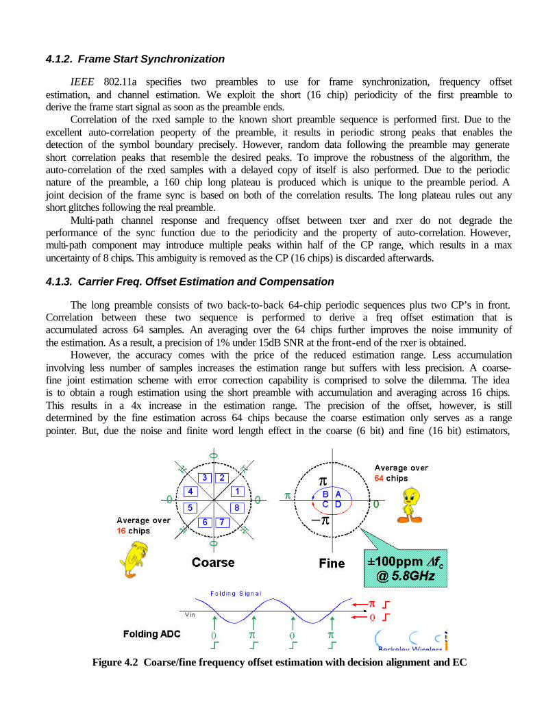
4.1.3. Carrier Freq. Offset Estimation and Compensation
The long preamble consists of two back-to-back 64-chip periodic sequences plus two CP’s in front. Correlation between these two sequence is performed to derive a freq offset estimation that is accumulated across 64 samples. An averaging over the 64 chips further improves the noise immunity of the estimation. As a result, a precision of 1% under 15dB SNR at the front-end of the rxer is obtained. However, the accuracy comes with the price of the reduced estimation range. Less accumulation involving less number of samples increases the estimation range but suffers with less precision. A coarse-fine joint estimation scheme with error correction capability is comprised to solve the dilemma. The idea is to obtain a rough estimation using the short preamble with accumulation and averaging across 16 chips. This results in a 4x increase in the estimation range. The precision of the offset, however, is still determined by the fine estimation across 64 chips because the coarse estimation only serves as a range pointer. But, due the noise and finite word length effect in the coarse (6 bit) and fine (16 bit) estimators,
Figure 4.2 Coarse/fine frequency offset estimation with decision alignment and EC
two estimations may not agree with each other right on the coarse boundaries where the fine estimation wraps around its [-π , π] range. Decision alignment error-correction scheme is proposed that solves the alignment problem. The situation is analogous to the “bit-alignment” scheme used in folding ADC’s to overcome the cross boundary ambiguity problem. Since the author had just finished his EE247 class project, in which he studied cascaded folding ADC in details, the error-correction method is directly ported to applied. The efficiency of the algorithm results in a robust yet accurate freq offset estimation module. The estimation range is also greatly enlarged to ±100ppm at 5.8GHz max carrier freq. Compensation is performed by a modified CORDIC algorithm, in which a modulo-2π up to ±5π (or ±100ppm) scheme is comprised to enable the usual CORDIC algorithm to handle large angles beyond ±π/2.
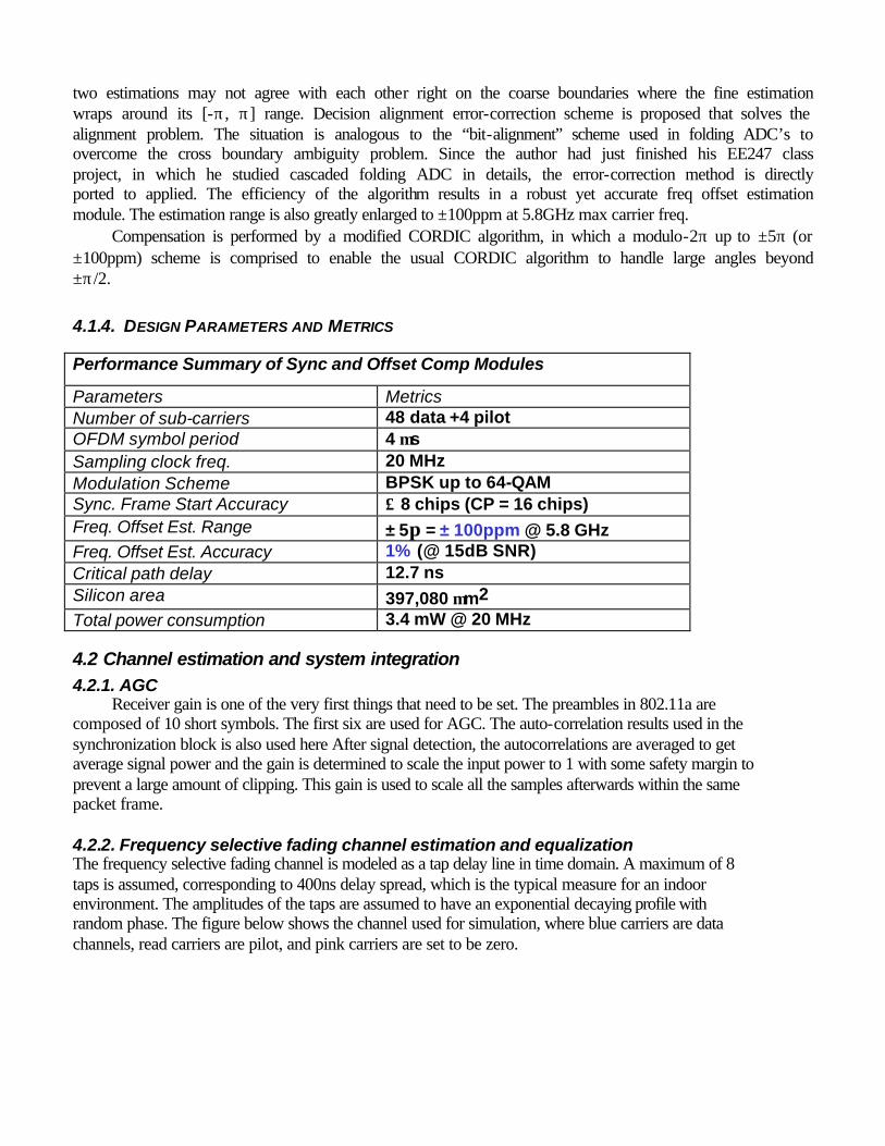
4.1.4. DESIGN PARAMETERS AND METRICS
Performance Summary of Sync and Offset Comp Modules
Parameters Metrics Number of sub-carriers 48 data +4 pilot OFDM symbol period 4 µs Sampling clock freq. 20 MHz Modulation Scheme BPSK up to 64-QAM Sync. Frame Start Accuracy ≤ 8 chips (CP = 16 chips) Freq. Offset Est. Range ± 5π = ± 100ppm @ 5.8 GHz Freq. Offset Est. Accuracy 1% (@ 15dB SNR) Critical path delay 12.7 ns Silicon area 397,080 µm2 Total power consumption 3.4 mW @ 20 MHz
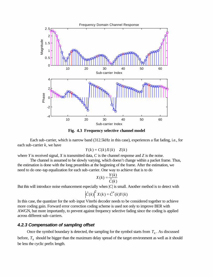
4.2 Channel estimation and system integration 4.2.1. AGC Receiver gain is one of the very first things that need to be set. The preambles in 802.11a are composed of 10 short symbols. The first six are used for AGC. The auto-correlation results used in the synchronization block is also used here After signal detection, the autocorrelations are averaged to get average signal power and the gain is determined to scale the input power to 1 with some safety margin to prevent a large amount of clipping. This gain is used to scale all the samples afterwards within the same packet frame. 4.2.2. Frequency selective fading channel estimation and equalization The frequency selective fading channel is modeled as a tap delay line in time domain. A maximum of 8 taps is assumed, corresponding to 400ns delay spread, which is the typical measure for an indoor environment. The amplitudes of the taps are assumed to have an exponential decaying profile with random phase. The figure below shows the channel used for simulation, where blue carriers are data channels, read carriers are pilot, and pink carriers are set to be zero.
10 20 30 40 50 600
0.5
1
1.5
2
2.5Frequency Domain Channel Response
Sub-carrier Index
Mag
nitu
de
10 20 30 40 50 60-4
-2
0
2
4
Sub-carrier Index
Pha
se
Fig. 4.3 Frequency selective channel model
Each sub-carrier, which is narrow band (312.5kHz in this case), experiences a flat fading, i.e., for
each sub-carrier k, we have )()()()( kZkXkCkY +=
where Y is received signal, X is transmitted data, C is the channel response and Z is the noise. The channel is assumed to be slowly varying, which doesn’t change within a packet frame. Thus,
the estimation is done with the long preambles at the beginning of the frame. After the estimation, we need to do one-tap equalization for each sub-carrier. One way to achieve that is to do
)(ˆ)(
)(kCkY
kX =
But this will introduce noise enhancement especially when |C| is small. Another method is to detect with
)()(ˆ)()(ˆ *2kYkCkXkC =
In this case, the quantizer for the soft-input Viterbi decoder needs to be considered together to achieve more coding gain. Forward error correction coding scheme is used not only to improve BER with AWGN, but more importantly, to prevent against frequency selective fading since the coding is applied across different sub-carriers.
4.2.3 Compensation of sampling offset Once the symbol boundary is detected, the sampling for the symbol starts from xT . As discussed before, xT should be bigger than the maximum delay spread of the target environment as well as it should be less the cyclic prefix length.
On the other hand, the receiver usually uses the peak energy correlation with the known pilot symbol to determine the symbol boundary. Due to the multi-path effect, the position of the peak is somewhere within the delay spread profile.
Using the transmitter time, assuming the peak correlation occurs at xτ which is an unknown quantity and combining this with the sampling time offset xT , the timing offset of the receiver is then
xxT τ+ which translates into a phase factor )(2 xxTfje τ+π
in frequency domain. Since in OFDM, data is encoded on the frequency domain sub-carrier Tkfk /= where k is sub-carrier index and T is the FFT symbol period. There is then a phase factor
)(2)(2 xxxx NNNkjT
Tk
jee
τ+πτ+π=
for each sub-carrier that must be compensated. Since xτ is unknown, this factor must be learned. Since there is unknown channel response for
each sub-carrier as well, this factor can be lumped into the unknown sub-carrier channel response, which is estimated using the long preambles. After performing FFT on the preambles, the frequency domain values are compared with the known preamble values to get the channel responses.
4.2.4 Frequency offset correction residual error The frequency offset correction is not perfect and the residual error tends to accumulate over samples. This residual error will cause orthogonality loss among sub-carriers. But this effect is minor since the accumulation is limited within a symbol. The accumulation is more prominent across symbols. There will be phase factor to each symbol due to the residual error. Four pilot sub-carriers are used for each data symbol to estimate the phase factor due to the residual error and ther carriers are then compensated.
4.2.5 BER simulation The Matlab/Simulink simulation parameters include:
• frequency offset (-100ppm to 100ppm) • frequency selective channel • simulation length
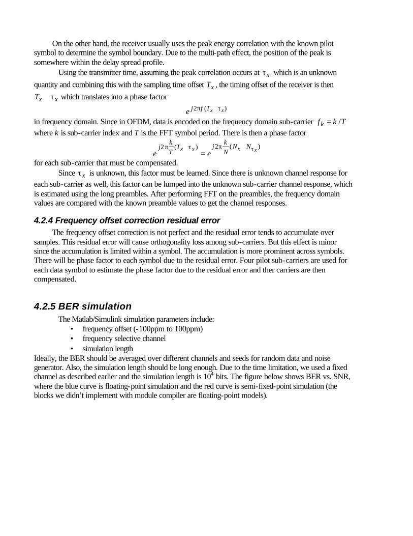
Ideally, the BER should be averaged over different channels and seeds for random data and noise generator. Also, the simulation length should be long enough. Due to the time limitation, we used a fixed channel as described earlier and the simulation length is 104 bits. The figure below shows BER vs. SNR, where the blue curve is floating-point simulation and the red curve is semi-fixed-point simulation (the blocks we didn’t implement with module compiler are floating-point models).
6 7 8 9 10 11 1210
-4
10-3
10-2
10-1
100
SNR (dB)
BE
R
Figure 4.4. BER simulation
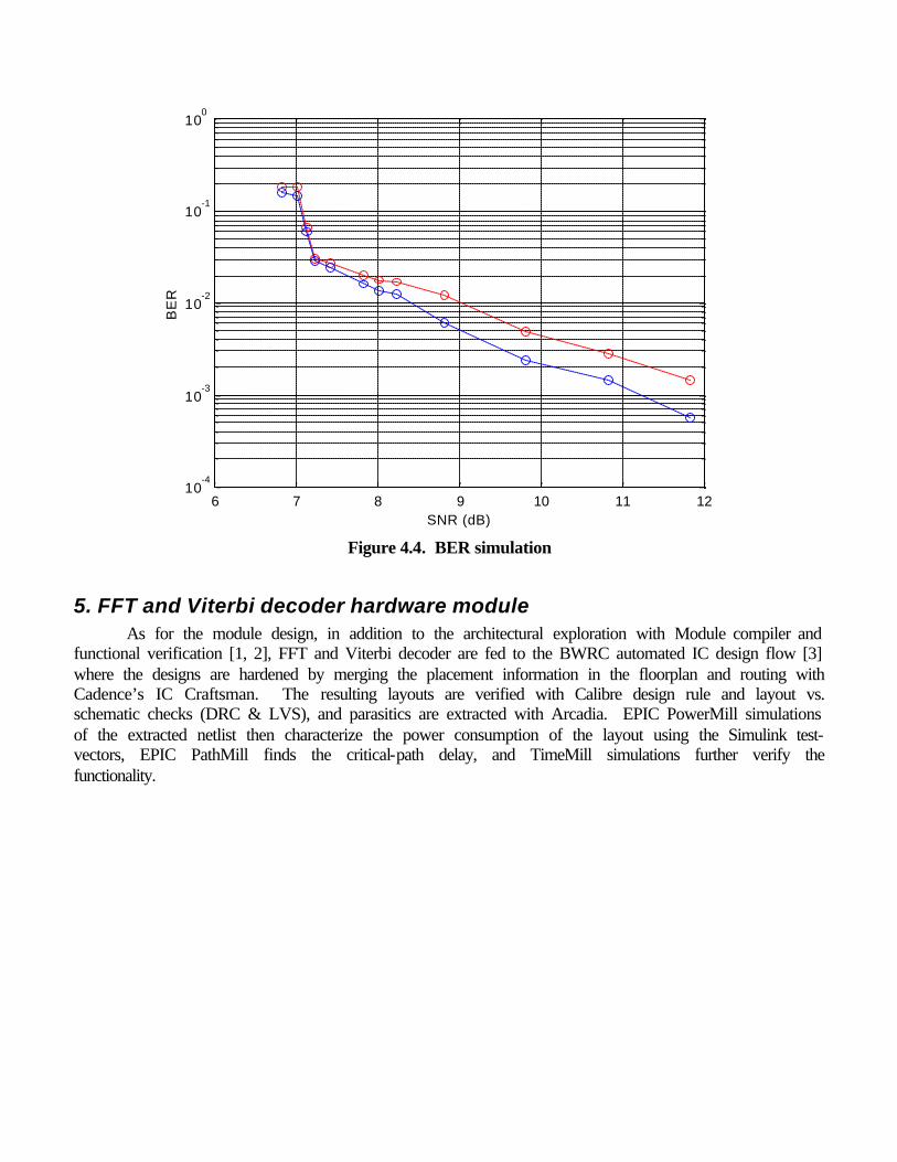
5. FFT and Viterbi decoder hardware module As for the module design, in addition to the architectural exploration with Module compiler and
functional verification [1, 2], FFT and Viterbi decoder are fed to the BWRC automated IC design flow [3] where the designs are hardened by merging the placement information in the floorplan and routing with Cadence’s IC Craftsman. The resulting layouts are verified with Calibre design rule and layout vs. schematic checks (DRC & LVS), and parasitics are extracted with Arcadia. EPIC PowerMill simulations of the extracted netlist then characterize the power consumption of the layout using the Simulink test-vectors, EPIC PathMill finds the critical-path delay, and TimeMill simulations further verify the functionality.
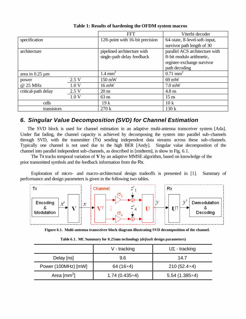
Table 1: Results of hardening the OFDM system macros
FFT Viterbi decoder specification 128-point with 16-bit precision 64-state, 8-level-soft-input,
survivor path length of 30 architecture pipelined architecture with
single-path delay feedback parallel ACS architecture with 8-bit modulo arithmetic, register-exchange survivor path decoding
area in 0.25 µm 1.4 mm2 0.71 mm2 2.5 V 150 mW 69 mW power
@ 25 MHz 1.0 V 16 mW 7.0 mW 2.5 V 20 ns 4.8 ns critical-path delay 1.0 V 63 ns 15 ns
cells 19 k 10 k transistors 270 k 130 k 6. Singular Value Decomposition (SVD) for Channel Estimation The SVD block is used for channel estimation in an adaptive multi-antenna transceiver system [Ada]. Under flat fading, the channel capacity is achieved by decomposing the system into parallel sub-channels through SVD, with the transmitter (Tx) sending independent data streams across these sub-channels. Typically one channel is not used due to the high BER [Andy]. Singular value decomposition of the channel into parallel independent sub-channels, as described in [midterm], is show in Fig. 6.1. The Tx tracks temporal variation of V by an adaptive MMSE algorithm, based on knowledge of the prior transmitted symbols and the feedback information from the Rx. Exploration of micro- and macro-architectural design tradeoffs is presented in [1]. Summary of performance and design parameters is given in the following two tables.
Table 6.1. MC Summary for 0.25µm technology (default design parameters)
V - tracking UΣ - tracking
Delay [ns] 9.6 14.7
Power (100MHz) [mW] 64 (16×4) 210 (52.4×4)
Area [mm2] 1.74 (0.435×4) 5.54 (1.385×4)
Figure 6.1. Multi-antenna transceiver block diagram illustrating SVD decomposition of the channel.
Summary of design parameters: • Wordlength (default w=8) • Adder type (default fat=”csa”) {cla, clsa, csa, ripple} • Multiplier type (default mut=”booth”) {booth, nonbooth}
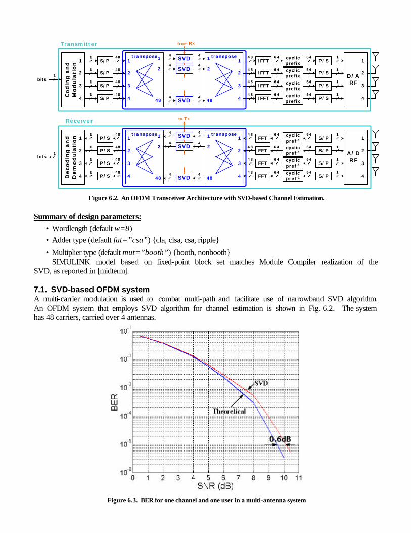
SIMULINK model based on fixed-point block set matches Module Compiler realization of the SVD, as reported in [midterm]. 7.1. SVD-based OFDM system A multi-carrier modulation is used to combat multi-path and facilitate use of narrowband SVD algorithm. An OFDM system that employs SVD algorithm for channel estimation is shown in Fig. 6.2. The system has 48 carriers, carried over 4 antennas.
481
2
4
3
1
2
48
transpose1
2
4
3
1
2
48
transposeSVD4 4
SVD4 4
SVD4 4
48
48
48
48
48
48
48
from Rx
S/P
S/P
S/P
S/PCo
din
g a
nd
Mo
du
lati
on
1
2
3
4
1
1
1
1
1bits
IFFT
IFFT
IFFT
IFFT
64
64
64
64
cyclicprefix
cyclicprefix
cyclicprefix
cyclicprefix
64
64
64
64
P/S
P/S
P/S
P/S
D/ARF
1
2
3
4
1
1
1
1
481
2
4
3
1
2
48
transpose1
2
4
3
1
2
48
transposeSVD4 4
SVD4 4
SVD4 448
48
48
48
48
48
48
to Tx
P/S
P/S
P/S
P/SDeco
din
g a
nd
Dem
od
ula
tio
n 1
2
3
4
1
1
1
1
1bits
FFT
FFT
FFT
FFT64
cyclicpref-1 S/P
S/P
S/P
S/P
A/DRF
1
2
3
4
1
1
1
1
cyclicpref-1
cyclicpref-1
cyclicpref-1
64
64
64
64
64
64
64
Transmitter
Receiver
Figure 6.2. An OFDM Transceiver Architecture with SVD-based Channel Estimation.
Figure 6.3. BER for one channel and one user in a multi-antenna system
Feasibility of the SVD tracking algorithms for U, Σ, and V is explored by BER simulations, using 100,000 long input bit stream. Simulation results are depicted in Fig. 6.3. It exhibits 0.6dB variation from ideal QPSK BER curve, at BER of 10-5. The V-tracking algorithm is placed and routed using the BWRC in-house automated design flow.
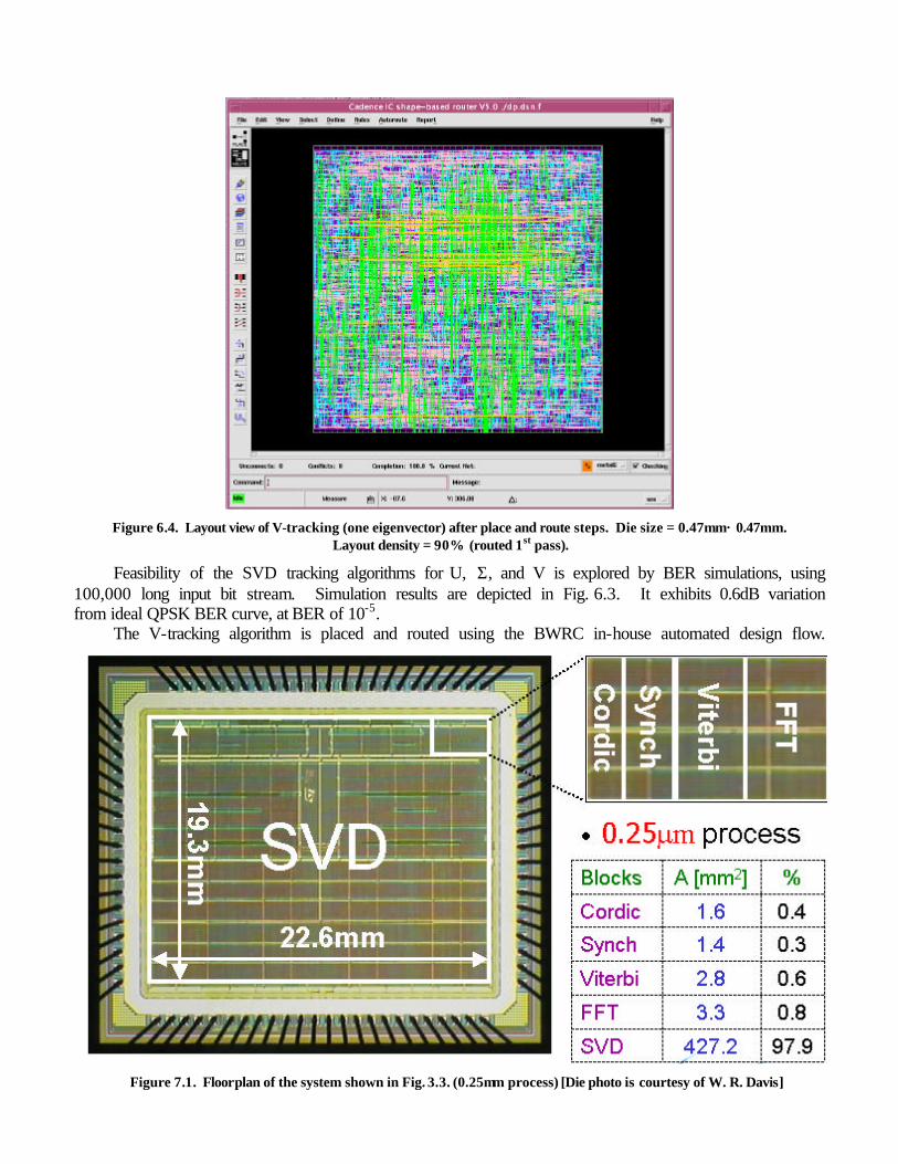
Figure 6.4. Layout view of V-tracking (one eigenvector) after place and route steps. Die size = 0.47mm× 0.47mm.
Layout density = 90% (routed 1st pass).
Figure 7.1. Floorplan of the system shown in Fig. 3.3. (0.25µm process) [Die photo is courtesy of W. R. Davis]
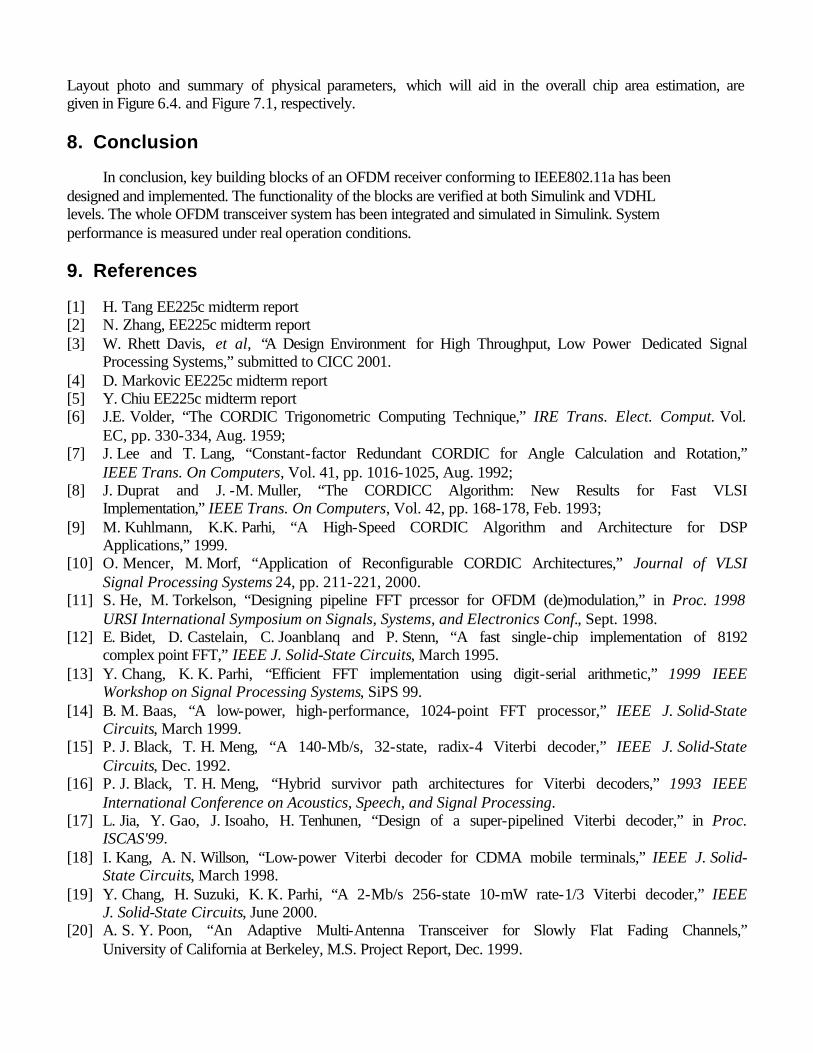
Layout photo and summary of physical parameters, which will aid in the overall chip area estimation, are given in Figure 6.4. and Figure 7.1, respectively. 8. Conclusion
In conclusion, key building blocks of an OFDM receiver conforming to IEEE802.11a has been designed and implemented. The functionality of the blocks are verified at both Simulink and VDHL levels. The whole OFDM transceiver system has been integrated and simulated in Simulink. System performance is measured under real operation conditions. 9. References
[1] H. Tang EE225c midterm report [2] N. Zhang, EE225c midterm report [3] W. Rhett Davis, et al, “A Design Environment for High Throughput, Low Power Dedicated Signal
Processing Systems,” submitted to CICC 2001. [4] D. Markovic EE225c midterm report [5] Y. Chiu EE225c midterm report [6] J.E. Volder, “The CORDIC Trigonometric Computing Technique,” IRE Trans. Elect. Comput. Vol.
EC, pp. 330-334, Aug. 1959; [7] J. Lee and T. Lang, “Constant-factor Redundant CORDIC for Angle Calculation and Rotation,”
IEEE Trans. On Computers, Vol. 41, pp. 1016-1025, Aug. 1992; [8] J. Duprat and J. -M. Muller, “The CORDICC Algorithm: New Results for Fast VLSI
Implementation,” IEEE Trans. On Computers, Vol. 42, pp. 168-178, Feb. 1993; [9] M. Kuhlmann, K.K. Parhi, “A High-Speed CORDIC Algorithm and Architecture for DSP
Applications,” 1999. [10] O. Mencer, M. Morf, “Application of Reconfigurable CORDIC Architectures,” Journal of VLSI
Signal Processing Systems 24, pp. 211-221, 2000. [11] S. He, M. Torkelson, “Designing pipeline FFT prcessor for OFDM (de)modulation,” in Proc. 1998
URSI International Symposium on Signals, Systems, and Electronics Conf., Sept. 1998. [12] E. Bidet, D. Castelain, C. Joanblanq and P. Stenn, “A fast single-chip implementation of 8192
complex point FFT,” IEEE J. Solid-State Circuits, March 1995. [13] Y. Chang, K. K. Parhi, “Efficient FFT implementation using digit-serial arithmetic,” 1999 IEEE
Workshop on Signal Processing Systems, SiPS 99. [14] B. M. Baas, “A low-power, high-performance, 1024-point FFT processor,” IEEE J. Solid-State
Circuits, March 1999. [15] P. J. Black, T. H. Meng, “A 140-Mb/s, 32-state, radix-4 Viterbi decoder,” IEEE J. Solid-State
Circuits, Dec. 1992. [16] P. J. Black, T. H. Meng, “Hybrid survivor path architectures for Viterbi decoders,” 1993 IEEE
International Conference on Acoustics, Speech, and Signal Processing. [17] L. Jia, Y. Gao, J. Isoaho, H. Tenhunen, “Design of a super-pipelined Viterbi decoder,” in Proc.
ISCAS'99. [18] I. Kang, A. N. Willson, “Low-power Viterbi decoder for CDMA mobile terminals,” IEEE J. Solid-
State Circuits, March 1998. [19] Y. Chang, H. Suzuki, K. K. Parhi, “A 2-Mb/s 256-state 10-mW rate-1/3 Viterbi decoder,” IEEE
J. Solid-State Circuits, June 2000. [20] A. S. Y. Poon, “An Adaptive Multi-Antenna Transceiver for Slowly Flat Fading Channels,”
University of California at Berkeley, M.S. Project Report, Dec. 1999.
[21] J. Ma, K. K. Parhi, and E. F. Deprettere, “An algorithm transformation approach to CORDIC based parallel singular value decompositions architectures,” in Proc. 33rd Asilomar Conf. on Signals, Systems, and Computers, pp. 1401-1405, Oct. 1999.
[22] M. Otte, M. Bucker, and J. Gotze, “Complex Cordic-Like Algorithms for Linearly Constrained MVDR Beamforming,” ?, 2000 IEEE
[23] O. Edfors et al., “OFDM Channel Estimation by Singular Value Decomposition,” IEEE Trans. Communications, vol. 46, pp. 931-939, July 1998.
[24] M. –H. Hsieh and C. –H. Wei, “Channel Estimation for OFDM Systems Based on Comb-Type Pilot Arrangement in Frequency Selective Fading Channels,” IEEE Trans. Consumer Electronics, pp. 217-225, Feb. 1998.
APPENDIX
OFDM group
Related Documents