~ ANALOG ~ DEVICES HighAccuracy, 22-Bit IntegratingAIDConverter FEATURES High Resolution: 22 Bits Wide Dynamic Range: 133dB Low Nonlinearity: Integral: :t 0.5ppm max Differential: :t 0.5LSB max High Stability: Gain: :!:1ppm/oC max Zero: :to.5J.lVrC max INL: :to.01ppmrC DNL: :!:O.OO25ppm/oC High Throughput Rate: 20 Conversions/Second Microprocessor Compatible Interface Compact Modular Package APPLICATIONS Data Acquisition Systems Scientific Instruments Medical Instruments Weighing Systems Automatic Test Equipment Test and Measurement Equipment GENERAL DESCRIPTION The AD 1175 is a very high resolution integrating A/D converter intended for applications that require the highest possible accuracy without sacrificing conversion speed, board space or modest pricing. This converter provides the performance of large bench top or rack mount instruments in a compact, modular package. The AD 1175 utilizes an auto-zeroed, multislope, integrating principle that features 22-bit resolution with extremely low nonlinearity (Integral: :!:O.5ppm max and Differential: :!:O.5LSB max). Temperature stability is specified at :!:O.5ppmrC maximum for gain (exclusive of reference), :!:0.5ILV/oC maximum for zero, :!:O.OlppmrC for integral nonlinearity, and:!: 0.0025ppm/oC for differential nonlinearity. The integration time is user selectable for maximum, line frequency noise rejection at either 60Hz or 50Hz. The conversion rate is 20 or 16 per second respectively, which is many times faster than benchtop instruments of similar performance. The nominal full-scale input range is :!:5V; however, rated accuracy is specified for inputs up to 10% over nominal, yielding a total dynamic range of greater than 4.6 million to I. The analog input is a high impedance, high CMRR, true differential input pair. The input low operates within:!: 100m V of analog ground and is used to sense signal low (at the source) to minimize ground loop problems. The output of the AD 1175 consists of four addressable 8-bit bytes (STATUS and 3 DATA) presented at an 8-bit tri-stated port with standard chip select. Information furnished by Analog Devices is believed to be accurate and reliable. However. no responsibility is assumed by Analog Devices for its use; nor for any infringements of patents or other rights of third parties which may result from its use. No license is granted by implica- tion or otherwise under any patent or patent rights of Analog Devices. Several modes of operation are available and allow writing to one of several addressable locations to program gain and offset, or to initiate a conversion. The AD 1175 requires no external components and operates from:!: l5V de and + 5V de power. All digital inputs and outputs are LSTTL compatible. The 3.7" x 5.2" x 0.53" metal case package provides excellent electrostatic and electromagnetic shielding. PRODUCT HIGHLIGHTS I. The unparalleled dynamic range, accuracy, linearity and stability of the AD 1175 represent a breakthrough for an A/D converter offering small size and modest cost. Only large, expensive bench top meters offer similar performance. 2. The AD1l75 converts approximately ten times as fast as digital meters with like performance. 3. The microprocessor interface of the AD1175 provides for straightforward operation, but with the features required for optimum system performance. Simple commands control offset adjust, gain adjust, external offset null and initiate conversions. The output bytes indicate input polarity, off-scale condition and a variety of additional status information. 4. The AD 1175 is a complete A/D converter including a precision internal reference, clock and integration capacitor. Offset and coarse gain adjust are bus controlled, while user accessible trim potentiometers allow fine gain adjust and:!: full-scale balance adjust. 5. Conversions may be made using either the offset and coarse gain settings stored in internal nonvolatile memory, or new settings made via the bus. The nonvolatile memory may be updated on command with the new settings. One Technology Way; P. O. Box 9106; Norwood, MA 02062-9106 U.S.A. Tel: 617/329-4700 Twx: 710/394-6577 Telex: 924491 Cables: ANALOG NORWOODMASS OBSOLETE

Welcome message from author
This document is posted to help you gain knowledge. Please leave a comment to let me know what you think about it! Share it to your friends and learn new things together.
Transcript
~ ANALOG~ DEVICES
HighAccuracy,22-BitIntegratingAIDConverter
FEATURESHigh Resolution: 22 BitsWide Dynamic Range: 133dBLow Nonlinearity:
Integral: :t 0.5ppm maxDifferential: :t 0.5LSB max
High Stability:Gain: :!:1ppm/oC maxZero: :to.5J.lVrC maxINL: :to.01ppmrCDNL: :!:O.OO25ppm/oC
High Throughput Rate: 20 Conversions/SecondMicroprocessor Compatible InterfaceCompact Modular Package
APPLICATIONS
Data Acquisition SystemsScientific InstrumentsMedical InstrumentsWeighing SystemsAutomatic Test EquipmentTest and Measurement Equipment
GENERAL DESCRIPTION
The AD 1175 is a very high resolution integrating A/D converterintended for applications that require the highest possible accuracywithout sacrificing conversion speed, board space or modestpricing. This converter provides the performance of large bench topor rack mount instruments in a compact, modular package.
The AD 1175 utilizes an auto-zeroed, multislope, integratingprinciple that features 22-bit resolution with extremely lownonlinearity (Integral: :!:O.5ppm max and Differential: :!:O.5LSBmax). Temperature stability is specified at :!:O.5ppmrC maximumfor gain (exclusive of reference), :!:0.5ILV/oC maximum for zero,:!:O.OlppmrC for integral nonlinearity, and:!: 0.0025ppm/oC fordifferential nonlinearity.
The integration time is user selectable for maximum, line frequencynoise rejection at either 60Hz or 50Hz. The conversion rate is
20 or 16 per second respectively, which is many times fasterthan benchtop instruments of similar performance.
The nominal full-scale input range is :!:5V; however, rated
accuracy is specified for inputs up to 10% over nominal, yieldinga total dynamic range of greater than 4.6 million to I. Theanalog input is a high impedance, high CMRR, true differentialinput pair. The input low operates within:!: 100m V of analogground and is used to sense signal low (at the source) to minimizeground loop problems.
The output of the AD 1175 consists of four addressable 8-bitbytes (STATUS and 3 DATA) presented at an 8-bit tri-statedport with standard chip select.
Information furnished by Analog Devices is believed to be accurateand reliable. However. no responsibility is assumed by Analog Devicesfor its use; nor for any infringements of patents or other rights of thirdparties which may result from its use. No license is granted by implica-tion or otherwise under any patent or patent rights of Analog Devices.
Several modes of operation are available and allow writing toone of several addressable locations to program gain and offset,or to initiate a conversion.
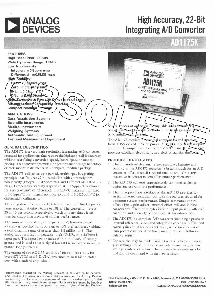
The AD 1175 requires no external components and operatesfrom:!: l5V de and + 5V de power. All digital inputs and outputsare LSTTL compatible. The 3.7" x 5.2" x 0.53" metal case packageprovides excellent electrostatic and electromagnetic shielding.
PRODUCT HIGHLIGHTS
I. The unparalleled dynamic range, accuracy, linearity andstability of the AD 1175 represent a breakthrough for an A/Dconverter offering small size and modest cost. Only large,expensive bench top meters offer similar performance.
2. The AD1l75 converts approximately ten times as fast asdigital meters with like performance.
3. The microprocessor interface of the AD1175 provides forstraightforward operation, but with the features required foroptimum system performance. Simple commands controloffset adjust, gain adjust, external offset null and initiateconversions. The output bytes indicate input polarity, off-scalecondition and a variety of additional status information.
4. The AD 1175 is a complete A/D converter including a precisioninternal reference, clock and integration capacitor. Offset andcoarse gain adjust are bus controlled, while user accessibletrim potentiometers allow fine gain adjust and:!: full-scalebalance adjust.
5. Conversions may be made using either the offset and coarsegain settings stored in internal nonvolatile memory, or newsettings made via the bus. The nonvolatile memory may beupdated on command with the new settings.
One Technology Way; P. O. Box 9106; Norwood, MA 02062-9106 U.S.A.Tel: 617/329-4700 Twx: 710/394-6577Telex: 924491 Cables: ANALOGNORWOODMASS
OBSOLETE
SPECIFICATIONS(tyPica'@+25°C,Model---------RESOLUTION
DYNAMIC RANGE
ACCURACY
Integral Nonlinearity'Differential Nonlinearity (~l 22 Bits)Total Noise (Ref to Input, 95% Confidence)
STABILITYGain T.e. (Excluding Reference)ZeroT.e.
Integral Nonlinearity T.e.Differential Nonlinearity T.e.
POWER SUPPLY REJECTION RATIO(", I5V)
WARMUP TIME
Relative Accuracy (for Rated Performance)Full Rated Performance
REFERENCEExternal Reference In
For Rated Performance
Maximum Input (Operating Only)Reference Output
VoltageOutput ResistanceTemperature CoefficientDrift with Time'
1st IS Days OperatingAfter IS Days Operation
Noise, 0.01 to JOHz (95% Confidence)User Reference Output
Gain (Referred to Reference In)Current
Stability: Temperature Coefficient
THROUGHPUTRATE6<!"Integrate Time of 1/30 sec (60Hz)(wIntegrate Time of 1/25 sec(50Hz)
ANALOG INPUT CHARACTERISTICS
Voltage Range7.,Max VINH (at Input Hi, Without Damage)Max V'NL (at Input Lo, Without Damage)Max V'NLR (Input Lo, for Rated Performance)Input Resistance (Input Hi, or Input Lo)Input BiasCurrent, Input Hi or Input Lo
( + JOoCto + 50°C)Input Bandwidth 9
Small SignalLarge Signal
CMRR at dc to 60Hz
ADJUSTMENTSOffset (Programmable)
RangeResolution
Gain-Coarse (Programmable)'RangeResolution
Gain-Fine RangeS.'Gain-Balance ('" Full Scale) RangeS
DIGITAL LEVELS
InputsLow
HighOutputs
Low(~14mA)High«!l JOOfLA)
POWER REQUIREMENTSSupply Voliages (for Rated Accuracy)
",Vs+Vo
Supply Current Drain~! '" I5V
After Warm-UpDuring Warm-Up
~l +5V
ENVIRONMENTALRated Performance
Operating
Size
Shielding
Weight
22-bits + 10%Overrange(4,600,000 Counts) min
133dB
'" 0.5ppm F.S.R.', max'" O.5LSB,max5fLVp-pmax
'" IppmRDG/oC,max"'O.5fLVrC,max"'O.OlppmF.S.R.'/oC'" 0.0025ppmF.S.R.'/oC
'" 5ppmF.S.R'iV
IS Minutes45 Minutes
+6.95V"'2%3+9.6V
+6.95 "'Z%Z500
'" OAppm/'C ('" 0.8ppmrC, max)
'" Ippm/Day'" Z5ppmlv'1000hrs., maxIppmp-p,max
l.000to1.0IZ'"'ZmA,max"'lfLV/oC,max
ZOconversions/sec16conversions/sec
'" 5V Bipolar'" 12V",3V'" JOOmVlOOOMO
'" JOnA, typ; '" 40nA, max
Z.OMHz150kHz80dB,min
",75mV
I LSB Steps
<4.7Vto>5.6V
0.009% Steps"'0.006%F.S.'" 0.005% F.S.
0.8V max2.0V min
OA5V maxZAV min
",I5V(",0.3Veach)+5V(-O.ZVto +OAV)
+ 55mA, - 70mAI5OmA175mA
JOOCto + 50°C, 70% RHOto+70'C- Z5°C to + 70°C
3.Tx5.2"xO.53"max
Electrostatic, 6 SidesElectromagnetic,S Sides170 grams
- + 5V unlessothelWise
NOTES
'Integtal Nonhnmity is specified ove< the enti" input span (NOMINAL FULL-SCALE + '0% Ove",nge).It is specified using the "End Point" definition, whm the moo is mm",ed afteo "moving the ofr." moo andthc gain mo," at plm and minus full "ale.
'FSR means Full Soak Range which = 10 vol".'Single ended, g<ound "fe",d.'Avmge t"nd hne.'Adiu"ment is penocmed v~ u"o a"",ible IO-tum "im potentiom"eo'Integoation Time is selwable to eith" 1/30", foc 60H, "iwion. 00 1/25 "c foe SOH, "jwion.'Thc Nominal Analog Input Voltagc Rangc is "V, but thc ADI175 may be eahbtated foe input voltag" f<om
,4.7V to,5.6V and maint.;n specified a"",,,y ove< thc cnti" tango. induding a 10% on-"ak ovmangc.Th"cfo", input voltag" of up to ,6.16V will be a"",ately convened whcn eahboated foe ,5.6V Nominal input.
'Conv"", "ction GAIN is digitally adiu"abk. via thc data bus. in "eps of 0.009% f<om <4.7 to >5.6V FSA um a"",iblc 10-tum "im potentiom"" is also p<ovidcd foe rmc GAIN adiu" (, 0.006% ..ngc).Alluni" acefactoryeahb..ted foc '5V NominalFull Scalcto within' 50eV
'Input Bandwid!h specifications a" foc tcuc integcation without""hpping.
Specifications subiw to changc without notice.
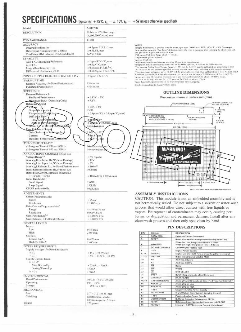
OUTLINE DIMENSIONSDimensions shown in inches and (mm),
NONCONOUCTIVE LABELTAIM.POTENTIOMETEAACCESS IFAA SIDEI
'-I'_J
NONCONDUCTtVEHEADEA
NOTE, SEEPAGE8FOAAECOMMENDEDSOCKET
ASSEMBLY INSTRUCTIONSCAUTION: This module is not an embedded assembly and isnot hermetically sealed, Do not subject to a solvent or water-washprocess that would allow dir.ect contact with free liquids orvapors, Entrapment of contaminants may occur, causing per-formance degradation and permanent damage, Install after anyclean/wash process and then only spot clean by hand,
PIN DESCRIPTIONS
-2-
PIN SIGNAL DESCRIPTION4 CONVCMD External ConvertCommand5 RESET Aeset Internal Microcomputer Following Pow eo-Up
60Hz/50HzWhen Set Low. Integration Time is 1/25 see
6 When Set High. Integration Time is 1/30 sec7 DONOTCDNNECT Used Only for Factooy Test8 +5V Digital Poweo Supply9.10 DIGGND Digital Ground (Both Pins are TiedTogetheolnternally)11-18 DBD-DB7 Bidirectional Data Bus (LSB-MSBI19 AD Address. Bit leco2D A1 Addoess. Bit One21 AD READ22 WA WRITE23 CS CHIP SELECT24 BUSY BUSY. Respondin9 to a Bus Command25 DATARDY DATA READY48.49 +15VRTN&GND Analog Power Ground and Case (Tied Together Internallyl58 ANAINLO Analog Input. Low59 ANAINHI Analog Input. High61 15V Negative Analog Power Supply62 SIGNALRTN Signal Rotum (Non.Cucrent Cacrying Groundl63 +15V Positive Analog Power Supply64 USERREFOUT Bulleoed Output of Reference at REF IN65 REFIN Reference Input. Noomally Connected to AEFOUT66 REF OUT Internal + 6.95V Refeoence Output. Unbulleoed
OBSOLETE
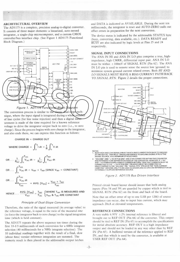
ARCHITECTURAL OVERVIEW
The AD 1175 is a complete, precision analog-to-digital converter.It consists of three major elements: a linearized, auto-zeroedintegrator, a single-chip microcomputer, and a custom CMOScontroller/bus interface chip. (See Figure I AD 1175 FunctionalBlock Diagram.)
4) CONV CMD
6) 60H.150H.
]) DO NOT CONNECT
Figure 1. AD1175 Functional Block Diagram
The conversion process is similar to the classic dual-slope tech-nique, where the input signal is integrated during a whole numberof line cycles (for line noise rejection) and then a digital meas-urement is made of the time required for a known referencevoltage to drive the integrator output back to zero (i.e., to zerocharge). Since the process begins with zero charge in the integrator,and also ends there, we can express this function as follows:
CHARGE IN = CHARGE OUT
WHERE CHARGE = i\ dt = ~ i\ dt
ITSIG
OR. .. -R' VS1G dtINT 0
, f TREF
R'NT Jo VREF dt
fTSIGOR, .. Jo VSIGdt = VREFX TREF(SINCE VREF= CONSTANT)
fTSIGOR. .. Jo VSIGdt
~ = AVG. [VSIG] = VREF x TREFTslG
HENCE... AVG. [VSIG] = TREF{WHERE TREFIS MEASURED AND
VREF TslG VREF& TslG ARE CONSTANT
Principle of Dual-Slope Conversion
Therefore, the ratio of the signal measured (its average value) tothe reference voltage, is equal to the ratio of the measuredtime(to force the integrator back to zero charge) to the signal integrationtime (which is held constant).
The AD 1175 repeats the above sequence ten times during thefirst 33-1/3 milliseconds of each conversion for a 60Hz integrateselection (40 milliseconds for a 50Hz integrate selection). The
10 individual readings together with the result of a final, slow(about 6ms) vernier reference integration are summed. Thenumeric result is then placed in the addressable output latches
and DATA is indicated as AYAILABLE. During the next tenmilliseconds, the integrator is reset and AUTO-ZERO nulls outoffset errors in preparation for the next conversion.
The device status is indicated by the addressable STATUS byte(busy, converting, data available, etc.). DATA READY andBUSY are also indicated by logic levels at Pins 25 and 24respectively.
SIGNAL INPUT CONNECTIONSThe ANA IN HI and ANA IN LO pins comprise a true, high-impedance, high CMRR, differential input pair. ANA IN LOmust be within:!: 1O0mYof SIGNAL RTN (Pin 62). The ANAIN La pin is used to remote sense the source low (ground) tominimize system ground current related errors. Both HI ANDLO SIGNALS MUST HAYE A BIAS CURRENT PATH BACKTO SIGNAL RTN. Figure 2 details the proper connections.
AD"]5"
A2
60H'f5ijH,~DONOTCONNECT(7
F---'I
II
I
62) SIGNALRTN /' ~: ISEENOTE"ANA IN HI I
I
58) ANA IN La ir J
D.
Do
READ
WRITE
BUS
DECODE
A"
NOTES1. BOTH HIGH AND LOW SIGNALS MUST HAVEA BIAS CURRENT PATH BACK TO GROUND
ATTHEAD1175. "ANA IN lO" SHOULD REFERENCE TO GROUND ISIGNAl RTNI ATTHESIGNAL SOURCE. VIA A MINIMUM OF RESISTANCE.
2. "DIG GND" AND" '"15V RTN& GND" ARE STAR CONNECTED WITHIN THE CONVERTER,AND INTENDED TO BE SEPARATE OUTSIDE OFTHE CONVERTER. HOWEVER,IF '" 15V
AND + 5V POWER SHARE A SINGLE COMMON RETURN. THEN THAT COMMON MUST BECONNECTED TO THE" '"15V RTN & GND" PIN WHICH MUST BE CONNECTED VIAHEAVY COPPER TO THE "DIG GND" PIN. "SIGNAL RTN" (PIN 6211S THE "NON-CURRENT
CARRYING" GROUND, ONLY TO BE USED AS SHOWN AND AS GROUND REFERENCE FOR ANEXTERN All Y SUPPLIED REFERENCE SOURCE.
Figure 2, AD 1175 Bus Driven Interface
Printed circuit board layout should insure that both analog
inputs (Pins 58 and 59) are guarded by copper which is tied toSIGNAL RTN (Pin 62) on the front and back of the board.
Note that an offset error of up to one LSB per l20n of sourceimpedance can occur, due to input bias current, which mayapproach 20nA at elevated temperatures.
REFERENCE CONNECTIONSA very stable 6.95Y :!:2% internal reference is filtered andbrought out to REF OUT (Pin 66) of the converter. This outputshould be tied to REF IN (Pin 65) to accomplish the specificationsfor initial absolute accuracy. REF OUT is a high impedanceoutput and should not be loaded in any way other than by REFIN (Pin 65). A buffered version of the reference applied to REFIN, and that which is used by the converter, is available atUSER REF OUT (Pin 64).
-3-
OBSOLETE
When making ratiometric measurements, where the sourceexcitation is derived from the converter reference, use the referencesignal present at USER REF OUT (Pin 64). The load appliedto Pin 64 should not exceed two milliamps. If an external referencesource is to be used, it should be applied to REF IN (Pin 65).
POWER SUPPLIES AND GROUNDS
The power supply pins are all well bypassed internally to theirrespective common or ground pins. The converter is very tolerantof dc and low frequency noise (slOOs of Hz) on any of thesupplies, as evidenced in the power supply rejection specifications.High frequency noise (::o:IMHz) in excess of 10mV on the:!: 15Vsupplies could, however, degrade the converter's performance.
To avoid large, digital-rate, circulating ground currents, thesystem's analog supply common and that of the digital supplyshould be kept separate and then tied together at the converterby a heavy track (to supplement that which is internal to theconverter) from:!: 15V RTN & GND (Pins 48 and 49) to DIGGND (Pins 9 & 10).
If the logic supply and analog supply share a single common,then that common should be brought to :!:15V RTN & GND(Pins 48 and 49) and then from these pins a heavy track shouldbe run to DIG GND (Pins 9 & 10).
RESET (Pin 5; Input)After power-up and before access may be made to the converter,a reset of the internal microcomputer must be accomplished.The RESET (Pin 5) may be driven from an external source,such as may exist in most computer-based systems, or it may beconnected to a simple RC circuit which will automatically generatea reset sequence upon power-up. See Figure 2 for the recommendedcircuit.
When driven from an external source, RESET must be heldhigh for a minimum of 3 microseconds, but must not terminatebefore the + 5V logic supply and the:!: 15V analog supply havebeen stable (> + 4.7V, and> :!:II V) for 300 microseconds.
60Hz/50Hz (Pin 6; Input)Pin 6 of the module selects either 33-1/3 milliseconds or 40
milliseconds for the signal integration time. This input is internallypulled up to 5V via IOkD.and may be left open for 60Hz normal-mode rejection. The pin should be connected to Digital Groundfor operation in a 50Hz line frequency environment.
CONY CMD (Pin 4; Input)A negative logic transition on this input causes a MODCONconversion to occur (see CALIBRATION section). A minimumhold time of 1.5/Lsis required at both the High and the Lowstates, to operate properly. The BUSY output (Pin 24) will notrespond, and BUSY (bit 0) of the STATUS word will not beindicated, but all other bits of the STATUS word will be active.DATA RDY (Pin 25) will occur per Figure 8.
This input is provided to allow externally triggered conversionswhich will use the temporarily programmed gain and offsetvalues (or the start-up defaults if no changes have been made).
DATA RDY (Pin 25; Output)
This signal will go to logic" I" when any conversion's new data
has become stable in the output latches. It will remain high forthe duration of the auto-zero phase (about 10 milliseconds) andgo low at the end of that phase (at the end of BUSY).
BUSY (Pin 24; Output)When a COMMAND byte is written to the microprocessorcompatible port, this line is set low and remains low for the
duration of the converter's response to that command. It is tHeopposite state of the BUSY bit within the STATUS byte.
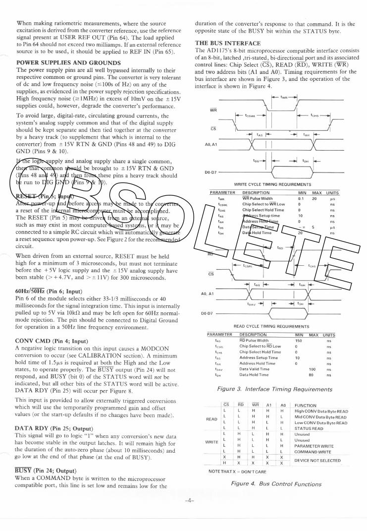
THE BUS INTERFACE
The AD 1175's 8-bit microprocessor compatible interface consistsof an 8-bit, latched ,tri-stated, bi-directional port and its associatedcontrol lines: Chip Select (CS), READ (RD), WRITE (WR)and two address bits (AI and AO). Timing requirements for thebus interface are shown in Figure 3, and the operation of theinterface is shown in Figure 4.
r- tWR~
WR j l- r- tCSWl I I I tCHS --1CS~ - r
=j tAgt- ~ tAHI;-J II JC
tOS-1 ~ ~ tOH r\ I
AO.A1
00-07
r- tR°-1RD \ 1
1- tCSRl J
1
- tCHS-1CS~ I r
::1 tAgf- ~ tAHt~I 1,[
tOAv -+I I+- -+I tOH r< 'j
AO. A1
00-07
READ CYCLE TIMING REQUIREMENTS
Figure 3. Interface Timing Requirements
READ
L
WRITE LLL
A1 I AD I FUNCTION- -c-- - -r--- .""
H H! High CONV Data Byte READ
H . L i Mid CONV Data Byte READL H' LowCONVDataByteREAD
L L I_STATUS READH H: UnusedH L I Unused
L .. H I PARAMETER WRITE
! L..-L L_~J,,(;..CJI'v1_~~D.."Y~ITE.._~.X
DEVICE NOT SELECTED
NOTE THAT X = DON'TCARE
Figure 4. Bus Control Functions
-4-
WRITE CYCLE TIMING REQUIREMENTS
PARAMETER DESCRIPTION MIN MAX UNITStWR WR Pulse Width 0.1 20 J.<s
toswl Chip Select to WR Low 0 ns
tCHS Chip Select Hold Time 0 ns
tAg Address Setup time 10 ns
tAH Address Hold Time 0 ns
tos Data Setup Time -x 5 J.<s
tOH Data Hold Time 20 ns
PARAMETER DESCRIPTION MIN MAX UNITS
tAD RD Pulse Width 150 ns
tCSAl Chip Select to RD Low 0 ns
tCHS Chip Select Hold Time 0 ns
tAg Address Setup Time 10 ns
tAH Address HoldTime 0 ns
tDAV Data Valid Time 100 ns
toH Data Hold Time 80 ns
OBSOLETE
BIT #
POS. OVERLOAD
+ 1.25 x FULL SCAL+ FULL SCALE+ 1/2 SCALE
ZERO
-1/2 SCALE- FULL SCALE
.=-~5 x FULLSCNEG. OVERLO,
Figure 5. Data Format
OUTPUT DATA FORMATThe result of a conversion is made available in three 8-bit bytes(addressed as shown in Figure 4). The numeric result is presentedas an offset binary number, where the offset value is equal to2en (40,00,00 Hex), i.e., zero volts input yields this numericaloutput. Therefore the nominal plus and minus full scale are2e22 ::!::2e21,or 60,00,00 Hex and 20,00,00 Hex respectively.For inputs greater than approximately 1.3 x nominal full scale,the converter will indicate an overload error (Bit 5 of theSTATUS
byte) and will also flag the occurrence by forcing all "l"s in theconversion result, i.e., FF,FF,FF Hex. Bit 23 (MSB) cannot bea "1" for any legitimate conversion result, so that bit is used toflag an overload. The data format is depicted in Figure 5.
COMMAND BYTEThe COMMAND BYTE allows eight different instructions tobe given. Five of these will require that a parameter be loadedinto the PARAMETER * register prior to writing the commandregister. The commands are written at address 00 (ADDRESSlines Al and AO, Pins 20 and 19 respectively) while a parameteris written to address 01. See Figure 4 for Bus Control Functions.Figure 8 details command timing requirements.
The commands are described below, preceded by an opcodename and the digital code (in hex). Figure 6 summarizes eachcommand and its execution time.
DEFCON fOOlDEFault CONversion initiates a conversion, using the gain andoffset values which are stored in the nonvolatile memory (power-up defaults).
MODCON [OlJMODified CONversion initiates a conversion using the gain andoffset values which have been modified (since power-up) as incommands 02 through 07 below.
NEWOS [02JNEW OffSet subtracts the result of the last conversion from all
subsequent MODCON conversions, i.e., acquire a new systemoffset. The maximum range of this offset is 65,536 codes(= ::!::75mV). Attempts to acquire an offset outside of this rangewill be ignored and BIT 5 and BIT 6 (Overload and commandbyte ERRor) will be set in the STATUS byte.
INCROS [03JINCRease OffSet alters the offset (in LSBs) used by MODCONin the positive direction by a number between zero and 255(decimal), which has already been written to PARAMETER*.
'The PARAMETER register retains the last word written to it. Any subsequentcommands will repeatedly use that PARAMETER until it is updated.
--
This may be performed repeatedlyuntil a maximum offset of+ 75mV has been reached, as indicated by an Overload/BITSresponse in the STATUS byte.
DECROS [04JDECRease OffSet alters the offset (in LSBs) used by MODCONin the negative direction by a number between zero and 255(decimal), which has already been written to PARAMETER*.This may be performed repeatedly until a maximum offset of- 75mV has been reached, as indicated by an Overload/BIT 5response in the STATUS byte.
INCGAN [05J
INCrease GAiN by N x 0.01%, where N (a decimal numberbetween 0 and 255) has already been written to PARAMETER*.This may be performed repeatedly until a maximum gain ( <4. 7Vfull scale) has been reached, as indicated by an Overload/BIT 5response in the STATUS byte. Further INCGAN commandswill have no other effect.
DECGAN [06J
DECrease GAiN by N x 0.01%, where N (a decimal numberbetween 0 and 255) has already been written to PARAMETER*.This may be performed repeatedly until a minimum gain (>5.6Vfull scale) has been reached, as indicated by an Overload/BIT 5response in the STATUS byte. Further DECGAN commandswill have no other effect.
UPDATE [07J
Takes the current modified gain and offset values and writesthem to nonvolatile memory as the new start-up defaults. Toenable this function, decimal 165 (AS in hex) must first beloaded into PARAMETER* - failure to do so will result in anERRor (BlT6) response in the STATUS byte.
Note: Codes other than 00 through 07 will do nothing, exceptcause an ERRor (BIT 6) response in the STATUS byte.
I- .~_I\JEM0~!C-J-~u~-~19!"~_[)E~(;.F!~TI9~_.~~_-~--
DEFCON ; Initiate a Convecsion Using the Power-UpI Default Offset and Gain
j InitiateaConversionUsingtheModifiedOff;~t !50;";;-and Gain Values
EXECUTION TIMEAPPROXIMATE)
MODCON
NEWOS
INCROS Increase the Offset Used by MODCON
DECROS Decrease the Offset Used by MODCON
INCGAN fncrease the Gain Used by MODCONConversions- - .. --. ._-Decrease the Gain Used by MODCON(;onVer~on~_-Write Most Recent Modified Offset &Gain
DECGAIIJ
UPDATE
Figure 6. Synopsis of Commands
-5-
OBSOLETE
THE STATUS BYTE
The STATUS byte contains eight bits of information about the
current statUs of the AD 1175. This byte may be examined bythe host processor at any time. The individual bits in the statUsbyte are assigned the following functions:
BIT 0
BIT I
BIT 2
BIT 3
BIT 4
BIT 5
BIT 6
BIT 7
The BUSY bit is always set when the COMMANDBYTE is written, and cleared when the initiated routinehas terminated. BUSY is also indicated at BUSY (Pin24) of the module.
The CONVerting bit is set when the converter is inthe active process of converting and computation. It isinitiated by writing DEFCON or MODCON to theCOMMAND-BYTE, or by a negative transition atCONY CMD (Pin 4).
The Data AVail able bit indicates that a new conversion
is complete and the result is in the output latches.This bit sets to "I" at the conclusion of the convertingprocess and remains" I" for the remainder of the mini-mum AUTO-ZERO time (about 10 milliseconds). It isreset to "0" at the end of BUSY.
The MODified bit, when set to "I", means that modifiedgain and offset values are being used for the currentconversion; i.e., a conversion initiated by MODCONor an external signal at CONY CMD (Pin 4).
The VALue bit responds to COMMANDS 02 through07 by setting to "I" at the end of BUSY, and remains
until the next write to the COMMAND byte. This bitsignals that a gain or offset value used by MODCONhas been altered, or that the current MODCON gainand offset values have been loaded to nonvolatile memoryas the new power-up defaults.
The Overload bit will be set following any conversionwhere the integrator has been exposed to an overloadvoltage. Following commands 03 through 06, it indicatesthat a parameter (gain or offset) has been incremented
to its maximum or minimum possible value (note thatfurther attempts to increment that parameter will notcause an overflow or underflow). Also, followingNEWOS (02) command, this bit implies that an attemptwas made, and ignored, to acquire an offset outside ofthe allowable range of :!:75m V.
The ERRor bit indicates one of the following: 1. ACOMMAND-BYTE was written which was not within
the allowable range of 00 to 07. 2. An update (07)command was attempted without the KEY number(165 decimal) having first been written to PARAMETERat ADDRESS 01. 3. A NEWOS (02) command was
attempted for a value outside the permissible range of:!:32,768 codes (>75mV) from zero.
The WaRMUP bit flags the three second time-oUttaken by the converter following RESET, to allow thereference and auto-zero circuits to settle. The converter
will not convert during this time.
87
Figure 7. The Status Byte -
CALIBRA nON
The AD 1175 is factory calibrated for plus and minus full scale
(2e21) to be within:!: 50fLV of five volts, absolute. Since theconverter will operate within specifications for inputs up to tenpercent over nominal full scale, those inputs between:!: 5.5Vwill be converted accurately. (See Figure 9 for typical linearityvs. inpUt voltage.)
To correct for system offset voltage (particularly larger offset
voltages - up to :!:75m V) the NEWOS (03) command subtractsthe result of the last conversion from all subsequent MODCONconversions. If source noise is a concern when making the offset
adjustment, follow a single NEWOS command with multipleMODCON conversions, average the results and adjust offsetincrementally using the INCROS (03) or DECROS (04)commands.
The INCGAN OSand DECGAN 06 commands are the coarse
gain increment and decrement controls respectively. The minimumgain attainable will require greater than 5.6V to achieve a full-scaleoutput. At maximum gain, less than 4.7V will be required toyield a full-scale indication. The user accessible GAIN AD}potentiometer is the vernier, or fine gain trim (10 tUrns, with atotal adjustment range of about :!:0.006% FS).
The modified offset and gain resulting from commands 02, 03,04, OSand 06 are used only when conversions are initiated byMODCON (command 01), or conversions triggered by a negativelogic transition at the CONY CMD (Pin 4 of the converter).This pin requires a minimum hold time of 1.5fLSat both theHigh and the Low states, in order to operate properly.
The GAIN AD} potentiometer changes the overall gain for bothpositive and negative inputs. The BAL AD} potentiometerchanges the gain for positive inpUts only and allows setting ofplus and minus full-scale tracking to within:!: Ippm.
To Calibrate the AD1l75:
1. Attach a calibration source and set its output to zero volts.
2. Perform MODCON conversions and null out any observedoffset (via external computation, or by executing one or moreof the AD1175's offset controlling commands: INCROS,DECROS and NEWOS).
3. Set the GAIN AD} potentiometer fully clockwise (10 tUrns,i.e., maximum gain).
4. Apply -a negative full-scale calibration voltage ( - 4. 7V to- 5.6V).
5. Using the INCGAN or DECGAN command, coarse adjust
the gain such that a subsequent MODCON conversion yieldsa result just larger than minus full scale. In other words, asubsequent DECGAN by 01 would just yield a result that isless than or equal to minus full scale.
6. Adjust the GAIN AD} potentiometer to yield the precisevalue desired by tUrning counterclockwise and observingconversion results. When the correct gain is reached, rotatethe potentiometer about 3 degrees in the opposite directionto remove the tension from its wiper.
7. Switch the polarity of the calibration source to positive.
8. Adjust the BAL AD} potentiometer to yield the same gain asthat achieved in Step 6 above.
9. Save the new offset value and coarse gain value, if you wantthem to become the power-up defaults, by performing UP-DATE (Command 07).
Note: See the COMMAND BYTE section for details of command
operation.
-6-
--- --- ---
OBSOLETE

SIGNAL INTEGAA nON
A COMMAND BYTE Initiated Conve..ion
COMMAND WAITE"
{" Conve..ion Uses
--, - - - - - MODHiedPa,amete..
- -,- - - - - -{lftheAnalOg InputisToola,ge
{lfTh",eisaCommandEHo,
I I I I I0 10 20 30 40 SOms
~~
B. COMMAND BYTE Initiated Change to Gain andlo' Offset
VAL
Ol
EAA
'NOTE: COMMAND WAITE Always Causes Aew"te olthe Enti'e STATUS Byte.Fo, Example: If the Ovedoad Bit (Oll is Setas the Aesult of a Conve..ion,It Will Aemain Set in the STATUS Byte UnH! the Next COMMAND WAITE.
C. CONVEATCOMMAND !pin 41 Initiated Conve..ion
STATUSBiTS
CONVEAT
COMMAND ~;USY I {INACTIVE
CONV
DAV
MOD
--, {"AnaIOglnput,dool.,ge
OL
I I I I I0 to 20 30 40 SOms
BUSY I I INACTIVE(PIN241 ,---r-
DATAADY ~(PIN251
Figure 8. Command Timing Requirements
LINEARITY ERROA
(ppmFS)
10%OVEA.AANGE
'DVEA.LOAD
': ~~-t~-===UOV ~FS 1.IFS -1.3FS1/2FS
_INPUT VOLTAGE-'OVERLOAD CONDITION IS INDICATED BY BIT S OF THE STATUS BYTEAND A "1" IN BIT 23 OF THE OUTPUT DATA BYTE.
Figure 9. Typical Linearity Transfer Function
FACTORY TESTING -Each AD 1175 converter is factory calibrated via test apparatus
designed and constructed by Analog Devices. The heart of thetest system is a digitally programmable voIrage reference capableof sub-ppm accuracy and stability. Calibration of the test systemis verified daily using the highest precision instruments com-mercially available, e.g., FLUKE* model nOA Kelvin Varleyvoltage divider (accurate to within ::I::O.lppml) and model 732Adc secondary voIrage standard (accurate to within ::I::1.5ppm ofthe international voir!).
IBM PC INTERFACEFigure 10 is an example of an AD 1175/IBM interface suitablefor the IBM PC, XT or AT** personal computers. In this case,the AD 1175 is interfaced in the I/O space; a DIP switch controlsthe specific location of the AD 1175 within the available addressspace.
D7IA2I
D6IA3I
D51A41
D4IAS!
D3IA61
D'IA71
D1IA81
DOIA91
+5V ,IBM PCiXT
.us
A91AW
A81A'31
A71A'41
A6IA'S!
ASlA'61
A4IA27I
AENIAlll
IOWIB'3I
iOR IB141E)~ii\ RD
COMMAND WAITE" Lr fI
BUSY~Ir1 {"valueiSChanged
J to the MAXIMIN
1
1-- --- - -. -.{
" NEW Offsetis>~75mV
A31A'81
A2IA291
A1IA301
AOIA3'1
Figure 10. ADl175 to IBM PC/XT/A T Interface
*FLUKE is a registered tradedmark of John Fluke ManufacturingCompany, Inc.
**IBM PClXTI AT is a trademark ofInternational Business Machines Corp.
ITraceableto the NATIONAL BUREAU OF STANDARDS
-7-
--
BUSY
CONV
DAV
STATUSBITS
MOD
Ol
EAA
BUSY(PIN 241
DATAADY(PIN2S)
OBSOLETE
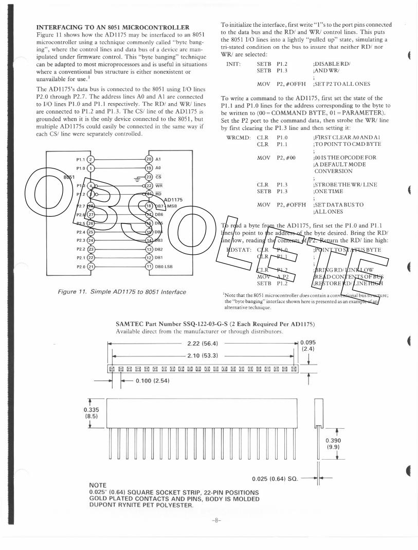
INTERFACING TO AN 8051 MICROCONTROLLERFigure II shows how the AD 1175 may be interfaced to an 8051microcontroller using a technique commonly called "byte bang-ing", where the control lines and data bus of a device are man-ipulated under firmware control. This "byte banging" techniquecan be adapted to most microprocessors and is useful in situationswhere a conventional bus structure is either nonexistent orunavailable for use. I
The AD 1175's data bus is connected to the 8051 using I/O linesP2.0 through P2.7. The address lines AOand Al are connectedto I/O lines PLO and PI. I respectively. The RD/ and WR/ linesare connected to Pl.2 and P1.3. The CS/ line of the AD1l75 is
grounded when it is the only device connected to the 8051, butmultiple AD 1175s could easily be connected in the same way ifeach CS/ line were separately controlled.
8051
Figure 11. Simple AD 1175 to BO51 Interface
To initialize the interface, first write" I"s to the port pins connec[eclto the data bus and the RD/ and WR/ control lines. This putsthe 8051 I/O lines into a lightly "pulled up" state, simulating atri-stated condition on the bus to insure that neither RD/ norWR/ are selected:
INIT: SETB PI.2SETB P1.3
4;DISABLE RDI;AND WR/
;SET P2 TO ALL ONES
To write a command to the AD1l75, first set the state of thePI. I and PLO lines for the address corresponding to the byte tobe written to (00 = COMMAND BYTE, 01 = PARAMETER).Set the P2 port to the command data, then strobe the WR/ lineby first clearing the Pl.3 line and then setting it:
WRCMD: CLR PI.O ;F1RSTCLEARAOANDAICLR Pl.l ;TOPOINTTOCMDBYTE
MOV P2, #OFFH
MOV P2, #00
CLR P1.3SETB P1.3
MOV P2, #OFFH
;00 IS THE arCaDE FOR;A DEFAULT MODECONVERSION
;STROBE THE WR/ LINE
;ONE TIME «
;SET DATA BUSTO;ALL ONES
To read a byte from the AD 1175, first set the PLO and PI. Ilines to point to the address of the byte desired. Bring the RD/line low, reading the contents of P2. Return the RD/ line high:
-8-
RDSTAT: CLRCLR
PI.OPI. I
;POINT TO STATUS BYTE
;BRING RDI LINE LOW;READ CONTENTS OF BUS;RESTORE RD/ LINE HIGH
4CLR PI.2
MOV A,P2SETB PI.2
'Note that the 8051 microcontroller does contain a conventional bus structure;the "byte banging" interface shown here is presented as an example of analternative technique.
SAMTEC Part Number SSQ-122-03-G-S (2 Each Required Per AD1l75)Available direct from the manufacturer or through distributors.
42.22 (56.4)
2.10 (53.3) l0.095(2.4)
~~~~~~~~~~~~~~~~~~~@~~~
0.100 (2.54)
r-0.335(8.5)~
T
--r0.390(9.9)
~
0.025 (O..OJ SO. ~~NOTE0.025" (0.64) SQUARE SOCKET STRIP, 22-PIN POSITIONSGOLD PLATED CONTACTS AND PINS, BODV IS MOLDEDDUPONT RVNITE PET POL VESTER.
4
OBSOLETE
Related Documents