For price, delivery, and to place orders, please contact Hittite Microwave Corporation: 20 Alpha Road, Chelmsford, MA 01824 Phone: 978-250-3343 Fax: 978-250-3373 Order On-line at www.hittite.com 11 11 - 178 LINEAR & POWER AMPLIFIERS - SMT HMC453QS16G / 453QS16GE InGaP HBT 1.6 WATT POWER AMPLIFIER, 0.4 - 2.2 GHz v01.0205 General Description Features Functional Diagram The HMC453QS16G & HMC453QS16GE are high dynamic range GaAs InGaP Heterojunction Bipo- lar Transistor (HBT) 1.6 watt MMIC power amplifiers operating between 0.4 and 2.2 GHz. Packaged in a miniature 16 lead QSOP plastic package, the amp- lifier gain is typically 21.5 dB at 0.4 GHz and 8 dB at 2.1 GHz. Utilizing a minimum number of external components and a single +5V supply, the amplifier output IP3 can be optimized to +47 dBm at 0.4 GHz or +51 dBm at 2.1 GHz. The power control (VPD) can be used for full power down or RF output power/ current control. The high output IP3 and PAE make the HMC453QS16G(E) ideal power amplifiers for Cellular/PCS/3G, WLL, ISM and Fixed Wireless applications. Output IP3: +51 dBm 21.5 dB Gain @ 400 MHz 8 dB Gain @ 2100 MHz 45% PAE @ +32 dBm Pout +25 dBm CDMA2000 Channel Power@ -45 dBc ACP Single +5V Supply Integrated Power Control (VPD) QSOP16G SMT Package: 29.4 mm 2 Electrical Specifications, T A = +25°C, Vs= +5V, VPD = +5V [1] Typical Applications The HMC453QS16G / HMC453QS16GE is ideal for applications requiring a high dynamic range amplifier: • GSM, GPRS & EDGE • CDMA & W-CDMA • CATV/Cable Modem • Fixed Wireless & WLL Parameter Min. Typ. Max. Min. Typ. Max. Min. Typ. Max. Min. Typ. Max. Min. Typ. Max. Units Frequency Range 400 - 410 450 - 496 810 - 960 1710 - 1990 2010 - 2170 MHz Gain 19 21.5 18 20.5 12 15 6 9 6 8 dB Gain Variation Over Temperature 0.012 0.02 0.012 0.02 0.012 0.02 0.012 0.02 0.012 0.02 dB / °C Input Return Loss 12 15 12 10 15 dB Output Return Loss 10 10 15 13 18 dB Output Power for 1dB Compression (P1dB) 29 32 29 32 29 32 28.5 31.5 30 33 dBm Saturated Output Power (Psat) 32.25 32.25 32.5 32 33.5 dBm Output Third Order Intercept (IP3) [2] 44 47 47 50 46 49 44 50 48 51 dBm Noise Figure 7 8.5 7 7.5 6.5 dB Supply Current (Icq) 725 725 725 725 725 mA Control Current (IPD) 12 12 12 12 12 mA [1] Specifications and data reflect HMC453QS16G measured using the respective application circuits for each designated frequency band found herein. Contact the HMC Applications Group for assistance in optimizing performance for your application. [2] Two-tone input power of -10 dBm per tone, 1 MHz spacing. Information furnished by Analog Devices is believed to be accurate and reliable. However, no responsibility is assumed by Analog Devices for its use, nor for any infringements of patents or other rights of third parties that may result from its use. Specifications subject to change without notice. No license is granted by implication or otherwise under any patent or patent rights of Analog Devices. Trademarks and registered trademarks are the property of their respective owners. For price, delivery, and to place orders: Analog Devices, Inc., One Technology Way, P.O. Box 9106, Norwood, MA 02062-9106 Phone: 781-329-4700 • Order online at www.analog.com Application Support: Phone: 1-800-ANALOG-D

Welcome message from author
This document is posted to help you gain knowledge. Please leave a comment to let me know what you think about it! Share it to your friends and learn new things together.
Transcript
For price, delivery, and to place orders, please contact Hittite Microwave Corporation:20 Alpha Road, Chelmsford, MA 01824 Phone: 978-250-3343 Fax: 978-250-3373
Order On-line at www.hittite.com
11
11 - 178
LIN
EA
R &
PO
WE
R A
MP
LIF
IER
S -
SM
THMC453QS16G / 453QS16GE
InGaP HBT 1.6 WATT POWER
AMPLIFIER, 0.4 - 2.2 GHz
v01.0205
General Description
Features
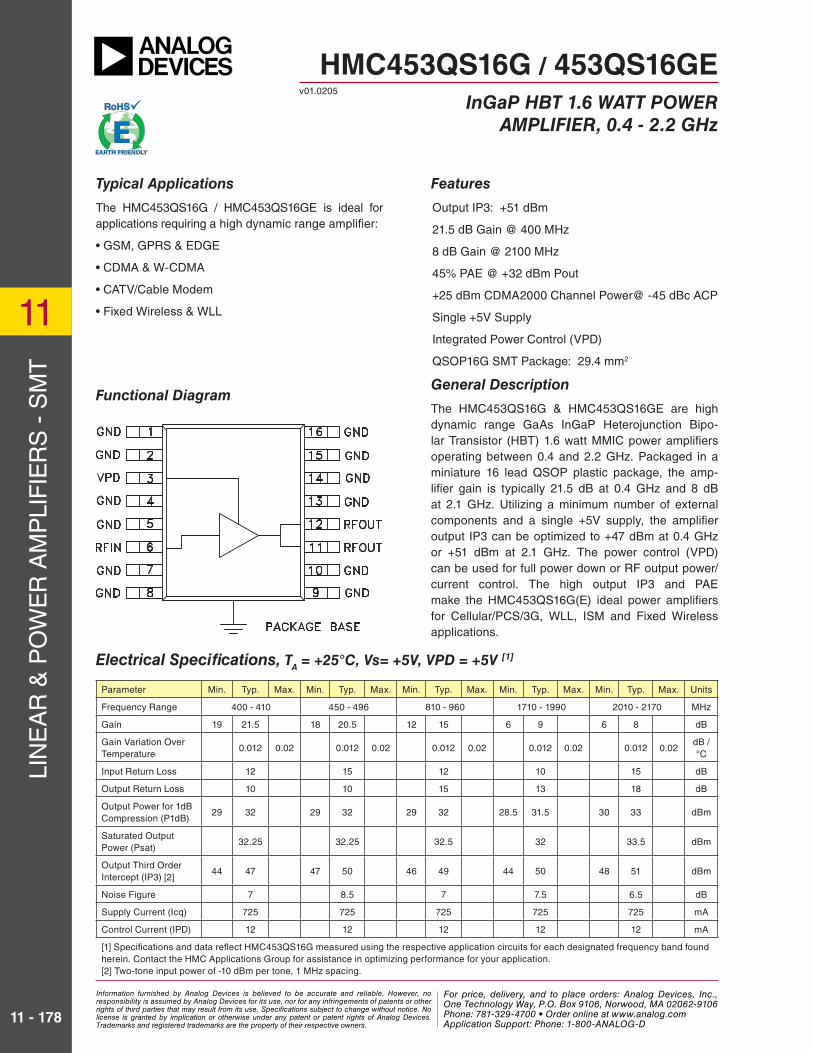
Functional DiagramThe HMC453QS16G & HMC453QS16GE are high dynamic range GaAs InGaP Heterojunction Bipo-lar Transistor (HBT) 1.6 watt MMIC power amplifi ers operating between 0.4 and 2.2 GHz. Packaged in a miniature 16 lead QSOP plastic package, the amp-lifi er gain is typically 21.5 dB at 0.4 GHz and 8 dB at 2.1 GHz. Utilizing a minimum number of external components and a single +5V supply, the amplifi er output IP3 can be optimized to +47 dBm at 0.4 GHz or +51 dBm at 2.1 GHz. The power control (VPD) can be used for full power down or RF output power/current control. The high output IP3 and PAE make the HMC453QS16G(E) ideal power amplifi ers for Cellular/PCS/3G, WLL, ISM and Fixed Wireless applications.
Output IP3: +51 dBm
21.5 dB Gain @ 400 MHz
8 dB Gain @ 2100 MHz
45% PAE @ +32 dBm Pout
+25 dBm CDMA2000 Channel Power@ -45 dBc ACP
Single +5V Supply
Integrated Power Control (VPD)
QSOP16G SMT Package: 29.4 mm2
Electrical Specifi cations, TA = +25°C, Vs= +5V, VPD = +5V [1]
Typical Applications
The HMC453QS16G / HMC453QS16GE is ideal for applications requiring a high dynamic range amplifi er:
• GSM, GPRS & EDGE
• CDMA & W-CDMA
• CATV/Cable Modem
• Fixed Wireless & WLL
Parameter Min. Typ. Max. Min. Typ. Max. Min. Typ. Max. Min. Typ. Max. Min. Typ. Max. Units
Frequency Range 400 - 410 450 - 496 810 - 960 1710 - 1990 2010 - 2170 MHz
Gain 19 21.5 18 20.5 12 15 6 9 6 8 dB
Gain Variation Over Temperature
0.012 0.02 0.012 0.02 0.012 0.02 0.012 0.02 0.012 0.02dB / °C
Input Return Loss 12 15 12 10 15 dB
Output Return Loss 10 10 15 13 18 dB
Output Power for 1dB Compression (P1dB)
29 32 29 32 29 32 28.5 31.5 30 33 dBm
Saturated Output Power (Psat)
32.25 32.25 32.5 32 33.5 dBm
Output Third Order Intercept (IP3) [2]
44 47 47 50 46 49 44 50 48 51 dBm
Noise Figure 7 8.5 7 7.5 6.5 dB
Supply Current (Icq) 725 725 725 725 725 mA
Control Current (IPD) 12 12 12 12 12 mA
[1] Specifi cations and data refl ect HMC453QS16G measured using the respective application circuits for each designated frequency band found herein. Contact the HMC Applications Group for assistance in optimizing performance for your application.[2] Two-tone input power of -10 dBm per tone, 1 MHz spacing.
Information furnished by Analog Devices is believed to be accurate and reliable. However, no responsibility is assumed by Analog Devices for its use, nor for any infringements of patents or other rights of third parties that may result from its use. Specifications subject to change without notice. No license is granted by implication or otherwise under any patent or patent rights of Analog Devices. Trademarks and registered trademarks are the property of their respective owners.
For price, delivery, and to place orders: Analog Devices, Inc., One Technology Way, P.O. Box 9106, Norwood, MA 02062-9106 Phone: 781-329-4700 • Order online at www.analog.com Application Support: Phone: 1-800-ANALOG-D
For price, delivery, and to place orders, please contact Hittite Microwave Corporation:20 Alpha Road, Chelmsford, MA 01824 Phone: 978-250-3343 Fax: 978-250-3373
Order On-line at www.hittite.com
LIN
EA
R &
PO
WE
R A
MP
LIF
IER
S -
SM
T
11
11 - 179
Input Return Loss
vs. Temperature @ 400 MHz
Output Return Loss
vs. Temperature @ 400 MHz
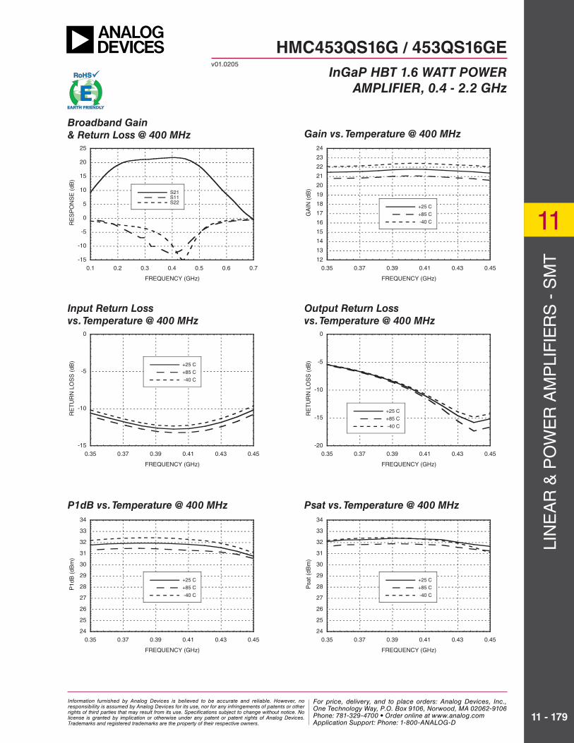
Broadband Gain
& Return Loss @ 400 MHz Gain vs. Temperature @ 400 MHz
P1dB vs. Temperature @ 400 MHz Psat vs. Temperature @ 400 MHz
-15
-10
-5
0
5
10
15
20
25
0.1 0.2 0.3 0.4 0.5 0.6 0.7
S21S11S22
RE
SP
ON
SE
(dB
)
FREQUENCY (GHz)
12
13
14
15
16
17
18
19
20
21
22
23
24
0.35 0.37 0.39 0.41 0.43 0.45
+25 C
+85 C
-40 C
GA
IN (
dB)
FREQUENCY (GHz)
-15
-10
-5
0
0.35 0.37 0.39 0.41 0.43 0.45
+25 C
+85 C
-40 C
RE
TU
RN
LO
SS
(dB
)
FREQUENCY (GHz)
-20
-15
-10
-5
0
0.35 0.37 0.39 0.41 0.43 0.45
+25 C
+85 C
-40 C
RE
TU
RN
LO
SS
(dB
)
FREQUENCY (GHz)
24
25
26
27
28
29
30
31
32
33
34
0.35 0.37 0.39 0.41 0.43 0.45
+25 C
+85 C
-40 C
P1d
B (
dBm
)
FREQUENCY (GHz)
24
25
26
27
28
29
30
31
32
33
34
0.35 0.37 0.39 0.41 0.43 0.45
+25 C
+85 C
-40 C
Psa
t (dB
m)
FREQUENCY (GHz)
HMC453QS16G / 453QS16GEv01.0205
InGaP HBT 1.6 WATT POWER
AMPLIFIER, 0.4 - 2.2 GHz
Information furnished by Analog Devices is believed to be accurate and reliable. However, no responsibility is assumed by Analog Devices for its use, nor for any infringements of patents or other rights of third parties that may result from its use. Specifications subject to change without notice. No license is granted by implication or otherwise under any patent or patent rights of Analog Devices. Trademarks and registered trademarks are the property of their respective owners.
For price, delivery, and to place orders: Analog Devices, Inc., One Technology Way, P.O. Box 9106, Norwood, MA 02062-9106 Phone: 781-329-4700 • Order online at www.analog.com Application Support: Phone: 1-800-ANALOG-D
For price, delivery, and to place orders, please contact Hittite Microwave Corporation:20 Alpha Road, Chelmsford, MA 01824 Phone: 978-250-3343 Fax: 978-250-3373
Order On-line at www.hittite.com
11
11 - 180
LIN
EA
R &
PO
WE
R A
MP
LIF
IER
S -
SM
T
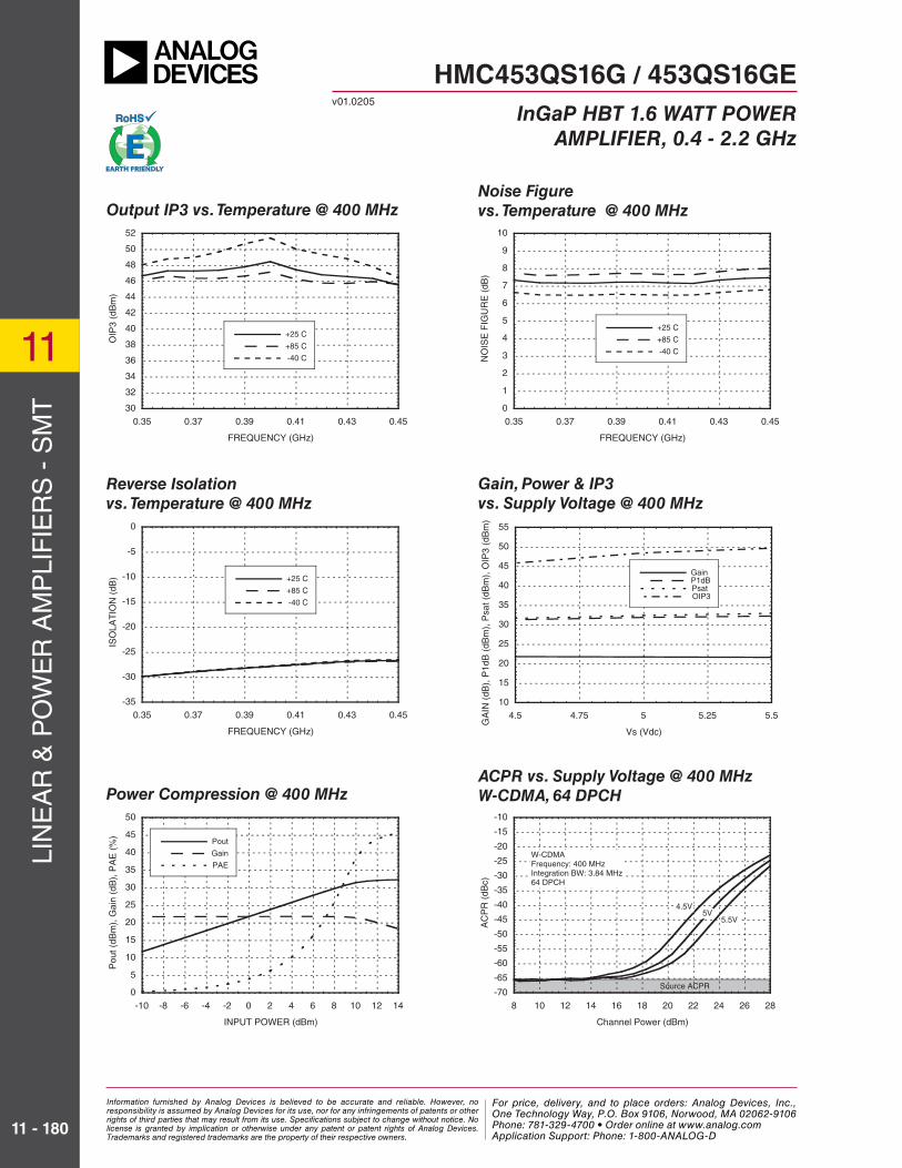
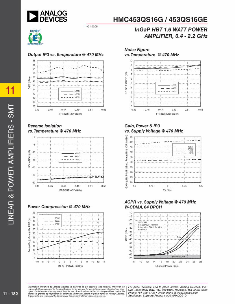
Output IP3 vs. Temperature @ 400 MHzNoise Figure
vs. Temperature @ 400 MHz
Gain, Power & IP3
vs. Supply Voltage @ 400 MHz
Reverse Isolation
vs. Temperature @ 400 MHz
ACPR vs. Supply Voltage @ 400 MHz
W-CDMA, 64 DPCH
10
15
20
25
30
35
40
45
50
55
4.5 4.75 5 5.25 5.5
GainP1dBPsatOIP3
GA
IN (
dB),
P1d
B (
dBm
), P
sat (
dBm
), O
IP3
(dB
m)
Vs (Vdc)
-35
-30
-25
-20
-15
-10
-5
0
0.35 0.37 0.39 0.41 0.43 0.45
+25 C
+85 C
-40 C
ISO
LAT
ION
(dB
)
FREQUENCY (GHz)
0
1
2
3
4
5
6
7
8
9
10
0.35 0.37 0.39 0.41 0.43 0.45
+25 C
+85 C
-40 C
NO
ISE
FIG
UR
E (
dB)
FREQUENCY (GHz)
30
32
34
36
38
40
42
44
46
48
50
52
0.35 0.37 0.39 0.41 0.43 0.45
+25 C
+85 C
-40 C
OIP
3 (d
Bm
)
FREQUENCY (GHz)
-70
-65
-60
-55
-50
-45
-40
-35
-30
-25
-20
-15
-10
8 10 12 14 16 18 20 22 24 26 28
AC
PR
(dB
c)
Channel Power (dBm)
W-CDMAFrequency: 400 MHzIntegration BW: 3.84 MHz64 DPCH
5V4.5V
5.5V
Source ACPR
HMC453QS16G / 453QS16GEv01.0205
Power Compression @ 400 MHz
0
5
10
15
20
25
30
35
40
45
50
-10 -8 -6 -4 -2 0 2 4 6 8 10 12 14
Pout
Gain
PAE
Pou
t (dB
m),
Gai
n (d
B),
PA
E (
%)
INPUT POWER (dBm)
InGaP HBT 1.6 WATT POWER
AMPLIFIER, 0.4 - 2.2 GHz
Information furnished by Analog Devices is believed to be accurate and reliable. However, no responsibility is assumed by Analog Devices for its use, nor for any infringements of patents or other rights of third parties that may result from its use. Specifications subject to change without notice. No license is granted by implication or otherwise under any patent or patent rights of Analog Devices. Trademarks and registered trademarks are the property of their respective owners.
For price, delivery, and to place orders: Analog Devices, Inc., One Technology Way, P.O. Box 9106, Norwood, MA 02062-9106 Phone: 781-329-4700 • Order online at www.analog.com Application Support: Phone: 1-800-ANALOG-D
For price, delivery, and to place orders, please contact Hittite Microwave Corporation:20 Alpha Road, Chelmsford, MA 01824 Phone: 978-250-3343 Fax: 978-250-3373
Order On-line at www.hittite.com
LIN
EA
R &
PO
WE
R A
MP
LIF
IER
S -
SM
T
11
11 - 181
Input Return Loss
vs. Temperature @ 40 MHz
Output Return Loss
vs. Temperature @ 470 MHz
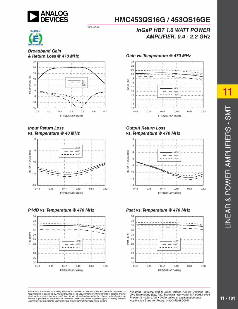
Broadband Gain
& Return Loss @ 470 MHz Gain vs. Temperature @ 470 MHz
P1dB vs. Temperature @ 470 MHz Psat vs. Temperature @ 470 MHz
-15
-10
-5
0
5
10
15
20
25
0.1 0.2 0.3 0.4 0.5 0.6 0.7
S21S11S22
RE
SP
ON
SE
(dB
)
FREQUENCY (GHz)
-14
-12
-10
-8
-6
-4
-2
0
0.43 0.45 0.47 0.49 0.51 0.53
+25C
+85C
-40C
RE
TU
RN
LO
SS
(dB
)
FREQUENCY (GHz)
-20
-15
-10
-5
0
0.43 0.45 0.47 0.49 0.51 0.53
+25C
+85C
-40C
RE
TU
RN
LO
SS
(dB
)
FREQUENCY (GHz)
24
25
26
27
28
29
30
31
32
33
34
0.43 0.45 0.47 0.49 0.51 0.53
+25C
+85C
-40C
Psa
t (dB
m)
FREQUENCY (GHz)
24
25
26
27
28
29
30
31
32
33
34
0.43 0.45 0.47 0.49 0.51 0.53
+25C
+85C
-40C
P1d
B (
dBm
)
FREQUENCY (GHz)
12
13
14
15
16
17
18
19
20
21
22
23
0.43 0.45 0.47 0.49 0.51 0.53
+25C
+85C
-40C
GA
IN (
dB)
FREQUENCY (GHz)
HMC453QS16G / 453QS16GEv01.0205
InGaP HBT 1.6 WATT POWER
AMPLIFIER, 0.4 - 2.2 GHz
Information furnished by Analog Devices is believed to be accurate and reliable. However, no responsibility is assumed by Analog Devices for its use, nor for any infringements of patents or other rights of third parties that may result from its use. Specifications subject to change without notice. No license is granted by implication or otherwise under any patent or patent rights of Analog Devices. Trademarks and registered trademarks are the property of their respective owners.
For price, delivery, and to place orders: Analog Devices, Inc., One Technology Way, P.O. Box 9106, Norwood, MA 02062-9106 Phone: 781-329-4700 • Order online at www.analog.com Application Support: Phone: 1-800-ANALOG-D
For price, delivery, and to place orders, please contact Hittite Microwave Corporation:20 Alpha Road, Chelmsford, MA 01824 Phone: 978-250-3343 Fax: 978-250-3373
Order On-line at www.hittite.com
11
11 - 182
LIN
EA
R &
PO
WE
R A
MP
LIF
IER
S -
SM
T 36
38
40
42
44
46
48
50
52
54
56
58
0.43 0.45 0.47 0.49 0.51 0.53
+25C
+85C
-40C
OIP
3 (d
Bm
)
FREQUENCY (GHz)
10
15
20
25
30
35
40
45
50
55
4.5 4.75 5 5.25 5.5
GainP1dBPsatOIP3
GA
IN (
dB),
P1d
B (
dBm
), P
sat (
dBm
), O
IP3
(dB
m)
Vs (Vdc)
-30
-25
-20
-15
-10
-5
0
0.43 0.45 0.47 0.49 0.51 0.53
+25C
+85C
-40C
ISO
LAT
ION
(dB
)
FREQUENCY (GHz)
0
1
2
3
4
5
6
7
8
9
10
0.43 0.45 0.47 0.49 0.51 0.53
+25C
+85C
-40C
NO
ISE
FIG
UR
E (
dB)
FREQUENCY (GHz)
Output IP3 vs. Temperature @ 470 MHzNoise Figure
vs. Temperature @ 470 MHz
Gain, Power & IP3
vs. Supply Voltage @ 470 MHz
Reverse Isolation
vs. Temperature @ 470 MHz
HMC453QS16G / 453QS16GEv01.0205
ACPR vs. Supply Voltage @ 470 MHz
W-CDMA, 64 DPCHPower Compression @ 470 MHz
0
5
10
15
20
25
30
35
40
45
50
55
-10 -8 -6 -4 -2 0 2 4 6 8 10 12 14
Pout
Gain
PAE
Pou
t (dB
m),
Gai
n (d
B),
PA
E (
%)
INPUT POWER (dBm)
-70
-65
-60
-55
-50
-45
-40
-35
-30
-25
-20
-15
-10
8 10 12 14 16 18 20 22 24 26 28
AC
PR
(dB
c)
Channel Power (dBm)
W-CDMAFrequency: 470 MHzIntegration BW: 3.84 MHz64 DPCH
5V4.5V
5.5V
Source ACPR
InGaP HBT 1.6 WATT POWER
AMPLIFIER, 0.4 - 2.2 GHz
Information furnished by Analog Devices is believed to be accurate and reliable. However, no responsibility is assumed by Analog Devices for its use, nor for any infringements of patents or other rights of third parties that may result from its use. Specifications subject to change without notice. No license is granted by implication or otherwise under any patent or patent rights of Analog Devices. Trademarks and registered trademarks are the property of their respective owners.
For price, delivery, and to place orders: Analog Devices, Inc., One Technology Way, P.O. Box 9106, Norwood, MA 02062-9106 Phone: 781-329-4700 • Order online at www.analog.com Application Support: Phone: 1-800-ANALOG-D
For price, delivery, and to place orders, please contact Hittite Microwave Corporation:20 Alpha Road, Chelmsford, MA 01824 Phone: 978-250-3343 Fax: 978-250-3373
Order On-line at www.hittite.com
LIN
EA
R &
PO
WE
R A
MP
LIF
IER
S -
SM
T
11
11 - 183
Input Return Loss
vs. Temperature @ 900 MHz
Output Return Loss
vs. Temperature @ 900 MHz
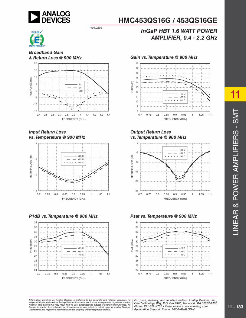
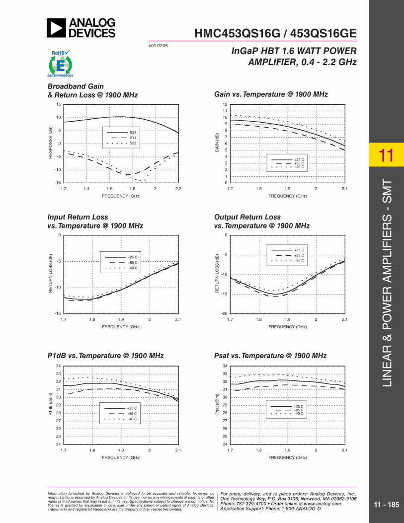
Broadband Gain
& Return Loss @ 900 MHz Gain vs. Temperature @ 900 MHz
P1dB vs. Temperature @ 900 MHz Psat vs. Temperature @ 900 MHz
-15
-10
-5
0
5
10
15
20
0.4 0.5 0.6 0.7 0.8 0.9 1 1.1 1.2 1.3 1.4
S21
S11
S22
RE
SP
ON
SE
(dB
)
FREQUENCY (GHz)
8
9
10
11
12
13
14
15
16
17
18
0.7 0.75 0.8 0.85 0.9 0.95 1 1.05 1.1
+25 C
+85 C
-40 C
GA
IN (
dB)
FREQUENCY (GHz)
-15
-10
-5
0
0.7 0.75 0.8 0.85 0.9 0.95 1 1.05 1.1
+25 C
+85 C
-40 C
RE
TU
RN
LO
SS
(dB
)
FREQUENCY (GHz)
-25
-20
-15
-10
-5
0
0.7 0.75 0.8 0.85 0.9 0.95 1 1.05 1.1
+25 C
+85 C
-40 C
RE
TU
RN
LO
SS
(dB
)
FREQUENCY (GHz)
24
25
26
27
28
29
30
31
32
33
34
0.7 0.75 0.8 0.85 0.9 0.95 1 1.05 1.1
+25 C
+85 C
-40 C
P1d
B (
dBm
)
FREQUENCY (GHz)
24
25
26
27
28
29
30
31
32
33
34
0.7 0.75 0.8 0.85 0.9 0.95 1 1.05 1.1
+25 C
+85 C
-40 C
Psa
t (dB
m)
FREQUENCY (GHz)
HMC453QS16G / 453QS16GEv01.0205
InGaP HBT 1.6 WATT POWER
AMPLIFIER, 0.4 - 2.2 GHz
Information furnished by Analog Devices is believed to be accurate and reliable. However, no responsibility is assumed by Analog Devices for its use, nor for any infringements of patents or other rights of third parties that may result from its use. Specifications subject to change without notice. No license is granted by implication or otherwise under any patent or patent rights of Analog Devices. Trademarks and registered trademarks are the property of their respective owners.
For price, delivery, and to place orders: Analog Devices, Inc., One Technology Way, P.O. Box 9106, Norwood, MA 02062-9106 Phone: 781-329-4700 • Order online at www.analog.com Application Support: Phone: 1-800-ANALOG-D
For price, delivery, and to place orders, please contact Hittite Microwave Corporation:20 Alpha Road, Chelmsford, MA 01824 Phone: 978-250-3343 Fax: 978-250-3373
Order On-line at www.hittite.com
11
11 - 184
LIN
EA
R &
PO
WE
R A
MP
LIF
IER
S -
SM
T
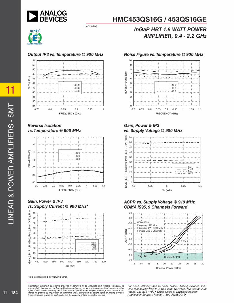
Output IP3 vs. Temperature @ 900 MHz Noise Figure vs. Temperature @ 900 MHz
Gain, Power & IP3
vs. Supply Voltage @ 900 MHz
Reverse Isolation
vs. Temperature @ 900 MHz
ACPR vs. Supply Voltage @ 910 MHz
CDMA IS95, 9 Channels Forward
34
36
38
40
42
44
46
48
50
52
54
0.75 0.8 0.85 0.9 0.95 1
+25 C
+85 C
-40 C
OIP
3 (d
Bm
)
FREQUENCY (GHz)
0
1
2
3
4
5
6
7
8
9
10
0.7 0.75 0.8 0.85 0.9 0.95 1 1.05 1.1
+25 C
+85 C
-40 C
NO
ISE
FIG
UR
E (
dB)
FREQUENCY (GHz)
-30
-25
-20
-15
-10
-5
0
0.7 0.75 0.8 0.85 0.9 0.95 1 1.05 1.1
+25 C
+85 C
-40 C
ISO
LAT
ION
(dB
)
FREQUENCY (GHz)
10
15
20
25
30
35
40
45
50
55
480 520 560 600 640 680 720 760 800
GainP1dBPsatOIP3
GA
IN (
dB),
P1d
B (
dBm
), P
sat (
dBm
), O
IP3
(dB
m)
Icq (mA)
10
15
20
25
30
35
40
45
50
55
4.5 4.75 5 5.25 5.5
GainP1dBPsatOIP3
GA
IN (
dB),
P1d
B (
dBm
), P
sat (
dBm
), O
IP3
(dB
m)
Vs (Vdc)
Gain, Power & IP3
vs. Supply Current @ 900 MHz*
-70
-65
-60
-55
-50
-45
-40
-35
-30
-25
12 14 16 18 20 22 24 26 28 30
AC
PR
(dB
c)
Channel Power (dBm)
Source ACPR
CDMA IS95Frequency: 910 MHzIntegration BW: 1.228 MHzForward Link, 9 Channels
5.5V
4.5V
5V
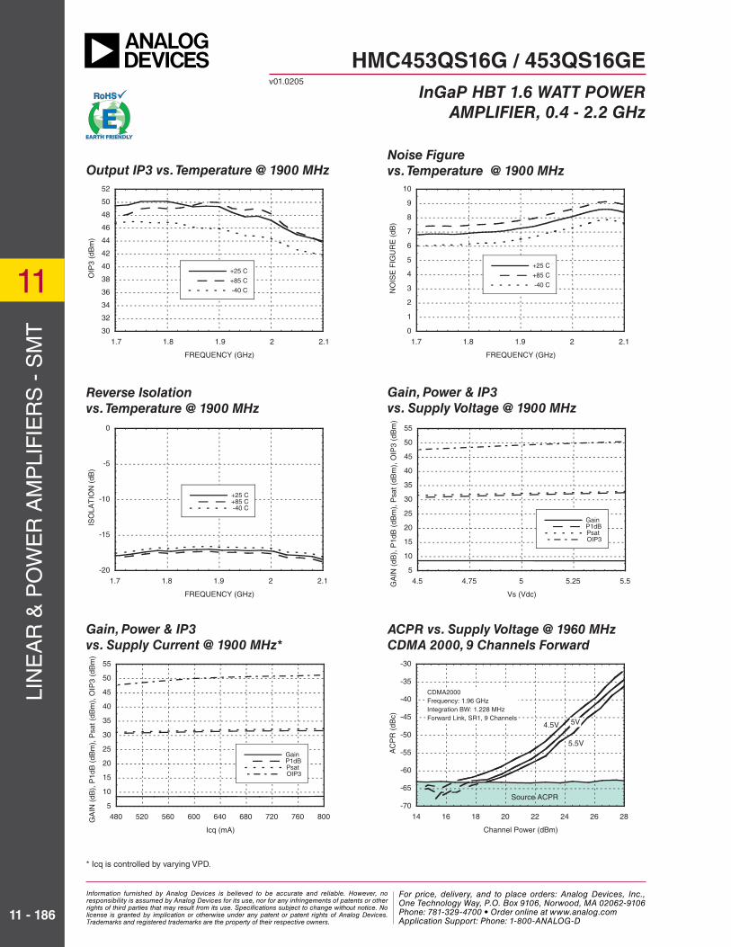
* Icq is controlled by varying VPD.
HMC453QS16G / 453QS16GEv01.0205
InGaP HBT 1.6 WATT POWER
AMPLIFIER, 0.4 - 2.2 GHz
Information furnished by Analog Devices is believed to be accurate and reliable. However, no responsibility is assumed by Analog Devices for its use, nor for any infringements of patents or other rights of third parties that may result from its use. Specifications subject to change without notice. No license is granted by implication or otherwise under any patent or patent rights of Analog Devices. Trademarks and registered trademarks are the property of their respective owners.
For price, delivery, and to place orders: Analog Devices, Inc., One Technology Way, P.O. Box 9106, Norwood, MA 02062-9106 Phone: 781-329-4700 • Order online at www.analog.com Application Support: Phone: 1-800-ANALOG-D
For price, delivery, and to place orders, please contact Hittite Microwave Corporation:20 Alpha Road, Chelmsford, MA 01824 Phone: 978-250-3343 Fax: 978-250-3373
Order On-line at www.hittite.com
LIN
EA
R &
PO
WE
R A
MP
LIF
IER
S -
SM
T
11
11 - 185
Input Return Loss
vs. Temperature @ 1900 MHz
Output Return Loss
vs. Temperature @ 1900 MHz
Broadband Gain
& Return Loss @ 1900 MHz Gain vs. Temperature @ 1900 MHz
P1dB vs. Temperature @ 1900 MHz Psat vs. Temperature @ 1900 MHz
-15
-10
-5
0
5
10
15
1.2 1.4 1.6 1.8 2 2.2
S21
S11
S22
RE
SP
ON
SE
(dB
)
FREQUENCY (GHz)
0
1
2
3
4
5
6
7
8
9
10
11
12
1.7 1.8 1.9 2 2.1
+25 C+85 C -40 C
GA
IN (
dB)
FREQUENCY (GHz)
-15
-10
-5
0
1.7 1.8 1.9 2 2.1
+25 C
+85 C
-40 C
RE
TU
RN
LO
SS
(dB
)
FREQUENCY (GHz)
-20
-15
-10
-5
0
1.7 1.8 1.9 2 2.1
+25 C
+85 C
-40 C
RE
TU
RN
LO
SS
(dB
)
FREQUENCY (GHz)
24
25
26
27
28
29
30
31
32
33
34
1.7 1.8 1.9 2 2.1
+25 C
+85 C
-40 C
P1d
B (
dBm
)
FREQUENCY (GHz)
24
25
26
27
28
29
30
31
32
33
34
1.7 1.8 1.9 2 2.1
+25 C+85 C -40 CP
sat (
dBm
)
FREQUENCY (GHz)
HMC453QS16G / 453QS16GEv01.0205
InGaP HBT 1.6 WATT POWER
AMPLIFIER, 0.4 - 2.2 GHz
Information furnished by Analog Devices is believed to be accurate and reliable. However, no responsibility is assumed by Analog Devices for its use, nor for any infringements of patents or other rights of third parties that may result from its use. Specifications subject to change without notice. No license is granted by implication or otherwise under any patent or patent rights of Analog Devices. Trademarks and registered trademarks are the property of their respective owners.
For price, delivery, and to place orders: Analog Devices, Inc., One Technology Way, P.O. Box 9106, Norwood, MA 02062-9106 Phone: 781-329-4700 • Order online at www.analog.com Application Support: Phone: 1-800-ANALOG-D
For price, delivery, and to place orders, please contact Hittite Microwave Corporation:20 Alpha Road, Chelmsford, MA 01824 Phone: 978-250-3343 Fax: 978-250-3373
Order On-line at www.hittite.com
11
11 - 186
LIN
EA
R &
PO
WE
R A
MP
LIF
IER
S -
SM
T
Output IP3 vs. Temperature @ 1900 MHzNoise Figure
vs. Temperature @ 1900 MHz
Gain, Power & IP3
vs. Supply Voltage @ 1900 MHzReverse Isolation
vs. Temperature @ 1900 MHz
ACPR vs. Supply Voltage @ 1960 MHz
CDMA 2000, 9 Channels Forward
Gain, Power & IP3
vs. Supply Current @ 1900 MHz*
30
32
34
36
38
40
42
44
46
48
50
52
1.7 1.8 1.9 2 2.1
+25 C
+85 C
-40 C
OIP
3 (d
Bm
)
FREQUENCY (GHz)
0
1
2
3
4
5
6
7
8
9
10
1.7 1.8 1.9 2 2.1
+25 C
+85 C
-40 C
NO
ISE
FIG
UR
E (
dB)
FREQUENCY (GHz)
-20
-15
-10
-5
0
1.7 1.8 1.9 2 2.1
+25 C+85 C -40 C
ISO
LAT
ION
(dB
)
FREQUENCY (GHz)
5
10
15
20
25
30
35
40
45
50
55
4.5 4.75 5 5.25 5.5
GainP1dBPsatOIP3
GA
IN (
dB),
P1d
B (
dBm
), P
sat (
dBm
), O
IP3
(dB
m)
Vs (Vdc)
5
10
15
20
25
30
35
40
45
50
55
480 520 560 600 640 680 720 760 800
GainP1dBPsatOIP3
GA
IN (
dB),
P1d
B (
dBm
), P
sat (
dBm
), O
IP3
(dB
m)
Icq (mA)
-70
-65
-60
-55
-50
-45
-40
-35
-30
14 16 18 20 22 24 26 28
AC
PR
(dB
c)
Channel Power (dBm)
Source ACPR
CDMA2000Frequency: 1.96 GHzIntegration BW: 1.228 MHzForward Link, SR1, 9 Channels
5.5V
4.5V 5V
* Icq is controlled by varying VPD.
HMC453QS16G / 453QS16GEv01.0205
InGaP HBT 1.6 WATT POWER
AMPLIFIER, 0.4 - 2.2 GHz
Information furnished by Analog Devices is believed to be accurate and reliable. However, no responsibility is assumed by Analog Devices for its use, nor for any infringements of patents or other rights of third parties that may result from its use. Specifications subject to change without notice. No license is granted by implication or otherwise under any patent or patent rights of Analog Devices. Trademarks and registered trademarks are the property of their respective owners.
For price, delivery, and to place orders: Analog Devices, Inc., One Technology Way, P.O. Box 9106, Norwood, MA 02062-9106 Phone: 781-329-4700 • Order online at www.analog.com Application Support: Phone: 1-800-ANALOG-D
For price, delivery, and to place orders, please contact Hittite Microwave Corporation:20 Alpha Road, Chelmsford, MA 01824 Phone: 978-250-3343 Fax: 978-250-3373
Order On-line at www.hittite.com
LIN
EA
R &
PO
WE
R A
MP
LIF
IER
S -
SM
T
11
11 - 187
Input Return Loss
vs. Temperature @ 2100 MHz
Output Return Loss
vs. Temperature @ 2100 MHz
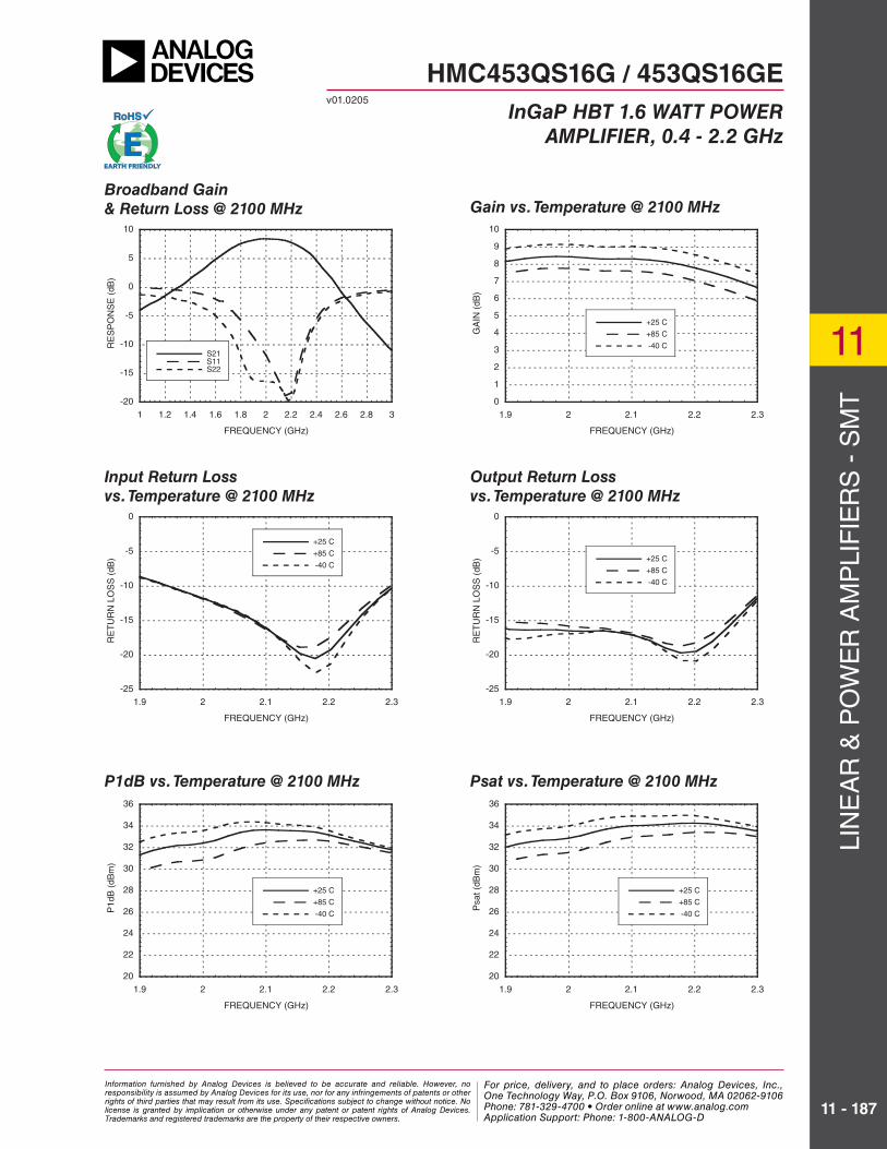
Broadband Gain
& Return Loss @ 2100 MHz Gain vs. Temperature @ 2100 MHz
P1dB vs. Temperature @ 2100 MHz Psat vs. Temperature @ 2100 MHz
-20
-15
-10
-5
0
5
10
1 1.2 1.4 1.6 1.8 2 2.2 2.4 2.6 2.8 3
S21S11S22
RE
SP
ON
SE
(dB
)
FREQUENCY (GHz)
-25
-20
-15
-10
-5
0
1.9 2 2.1 2.2 2.3
+25 C
+85 C
-40 C
RE
TU
RN
LO
SS
(dB
)
FREQUENCY (GHz)
-25
-20
-15
-10
-5
0
1.9 2 2.1 2.2 2.3
+25 C
+85 C
-40 C
RE
TU
RN
LO
SS
(dB
)
FREQUENCY (GHz)
20
22
24
26
28
30
32
34
36
1.9 2 2.1 2.2 2.3
+25 C
+85 C
-40 CP1d
B (
dBm
)
FREQUENCY (GHz)
20
22
24
26
28
30
32
34
36
1.9 2 2.1 2.2 2.3
+25 C
+85 C
-40 C
Psa
t (dB
m)
FREQUENCY (GHz)
0
1
2
3
4
5
6
7
8
9
10
1.9 2 2.1 2.2 2.3
+25 C
+85 C
-40 C
GA
IN (
dB)
FREQUENCY (GHz)
HMC453QS16G / 453QS16GEv01.0205
InGaP HBT 1.6 WATT POWER
AMPLIFIER, 0.4 - 2.2 GHz
Information furnished by Analog Devices is believed to be accurate and reliable. However, no responsibility is assumed by Analog Devices for its use, nor for any infringements of patents or other rights of third parties that may result from its use. Specifications subject to change without notice. No license is granted by implication or otherwise under any patent or patent rights of Analog Devices. Trademarks and registered trademarks are the property of their respective owners.
For price, delivery, and to place orders: Analog Devices, Inc., One Technology Way, P.O. Box 9106, Norwood, MA 02062-9106 Phone: 781-329-4700 • Order online at www.analog.com Application Support: Phone: 1-800-ANALOG-D
For price, delivery, and to place orders, please contact Hittite Microwave Corporation:20 Alpha Road, Chelmsford, MA 01824 Phone: 978-250-3343 Fax: 978-250-3373
Order On-line at www.hittite.com
11
11 - 188
LIN
EA
R &
PO
WE
R A
MP
LIF
IER
S -
SM
T
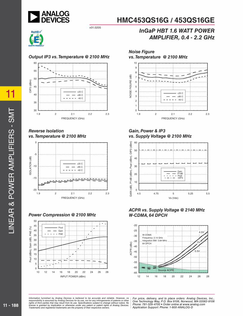
Output IP3 vs. Temperature @ 2100 MHzNoise Figure
vs. Temperature @ 2100 MHz
Gain, Power & IP3
vs. Supply Voltage @ 2100 MHz
Reverse Isolation
vs. Temperature @ 2100 MHz
0
10
20
30
40
50
60
4.5 4.75 5 5.25 5.5
GainP1dBPsatOIP3
GA
IN (
dB),
P1d
B (
dBm
), P
sat (
dBm
), O
IP3
(dB
m)
Vs (Vdc)
-20
-15
-10
-5
0
1.9 2 2.1 2.2 2.3
+25 C
+85 C
-40 C
ISO
LAT
ION
(dB
)
FREQUENCY (GHz)
0
1
2
3
4
5
6
7
8
9
10
1.9 2 2.1 2.2 2.3
+25 C
+85 C
-40 C
NO
ISE
FIG
UR
E (
dB)
FREQUENCY (GHz)
30
35
40
45
50
55
60
1.9 2 2.1 2.2 2.3
+25 C
+85 C
-40 C
OIP
3 (d
Bm
)
FREQUENCY (GHz)
HMC453QS16G / 453QS16GEv01.0205
ACPR vs. Supply Voltage @ 2140 MHz
W-CDMA, 64 DPCHPower Compression @ 2100 MHz
0
5
10
15
20
25
30
35
40
45
50
10 12 14 16 18 20 22 24 26 28
Pout
Gain
PAE
Pou
t (dB
m),
Gai
n (d
B),
PA
E (
%)
INPUT POWER (dBm)
-65
-60
-55
-50
-45
-40
-35
-30
-25
-20
12 14 16 18 20 22 24 26 28
AC
PR
(dB
c)
Source ACPR
W-CDMAFrequency: 2.14 GHzIntegration BW: 3.84 MHz64 DPCH 5V
5.5V
4.5V
InGaP HBT 1.6 WATT POWER
AMPLIFIER, 0.4 - 2.2 GHz
Information furnished by Analog Devices is believed to be accurate and reliable. However, no responsibility is assumed by Analog Devices for its use, nor for any infringements of patents or other rights of third parties that may result from its use. Specifications subject to change without notice. No license is granted by implication or otherwise under any patent or patent rights of Analog Devices. Trademarks and registered trademarks are the property of their respective owners.
For price, delivery, and to place orders: Analog Devices, Inc., One Technology Way, P.O. Box 9106, Norwood, MA 02062-9106 Phone: 781-329-4700 • Order online at www.analog.com Application Support: Phone: 1-800-ANALOG-D
For price, delivery, and to place orders, please contact Hittite Microwave Corporation:20 Alpha Road, Chelmsford, MA 01824 Phone: 978-250-3343 Fax: 978-250-3373
Order On-line at www.hittite.com
LIN
EA
R &
PO
WE
R A
MP
LIF
IER
S -
SM
T
11
11 - 189
Outline Drawing
Absolute Maximum Ratings
Collector Bias Voltage (Vcc) +6.0 Vdc
Control Voltage (Vpd) +5.4 Vdc
RF Input Power (RFIN)(Vs = Vpd = +5Vdc) +32 dBm
Junction Temperature 150 °C
Continuous Pdiss (T = 85 °C)(derate 58.5 mW/°C above 85 °C)
3.8 W
Thermal Resistance(junction to ground paddle)
17.1 °C/W
Storage Temperature -65 to +150 °C
Operating Temperature -40 to +85 °C
NOTES:
1. LEADFRAME MATERIAL: COPPER ALLOY
2. DIMENSIONS ARE IN INCHES [MILLIMETERS]
3. DIMENSION DOES NOT INCLUDE MOLDFLASH OF 0.15mm PER SIDE.
4. DIMENSION DOES NOT INCLUDE MOLDFLASH OF 0.25mm PER SIDE.
5. ALL GROUND LEADS AND GROUND PADDLE MUST BE SOLDERED TO
PCB RF GROUND.
1
1.5
2
2.5
3
3.5
4
4.5
0 5 10 15 20 25
PO
WE
R D
ISS
IPA
TIO
N (
W)
INPUT POWER (dBm)
Max Pdiss @ +85C
900 MHz
1900 MHz
Power Dissipation
Part Number Package Body Material Lead Finish MSL Rating Package Marking [3]
HMC453QS16G Low Stress Injection Molded Plastic Sn/Pb Solder MSL1 [1] H453XXXX
HMC453QS16GE RoHS-compliant Low Stress Injection Molded Plastic 100% matte Sn MSL1 [2] H453XXXX
[1] Max peak refl ow temperature of 235 °C[2] Max peak refl ow temperature of 260 °C[3] 4-Digit lot number XXXX
Package Information
HMC453QS16G / 453QS16GEv01.0205
InGaP HBT 1.6 WATT POWER
AMPLIFIER, 0.4 - 2.2 GHz
ELECTROSTATIC SENSITIVE DEVICEOBSERVE HANDLING PRECAUTIONS
Information furnished by Analog Devices is believed to be accurate and reliable. However, no responsibility is assumed by Analog Devices for its use, nor for any infringements of patents or other rights of third parties that may result from its use. Specifications subject to change without notice. No license is granted by implication or otherwise under any patent or patent rights of Analog Devices. Trademarks and registered trademarks are the property of their respective owners.
For price, delivery, and to place orders: Analog Devices, Inc., One Technology Way, P.O. Box 9106, Norwood, MA 02062-9106 Phone: 781-329-4700 • Order online at www.analog.com Application Support: Phone: 1-800-ANALOG-D
For price, delivery, and to place orders, please contact Hittite Microwave Corporation:20 Alpha Road, Chelmsford, MA 01824 Phone: 978-250-3343 Fax: 978-250-3373
Order On-line at www.hittite.com
11
11 - 190
LIN
EA
R &
PO
WE
R A
MP
LIF
IER
S -
SM
T
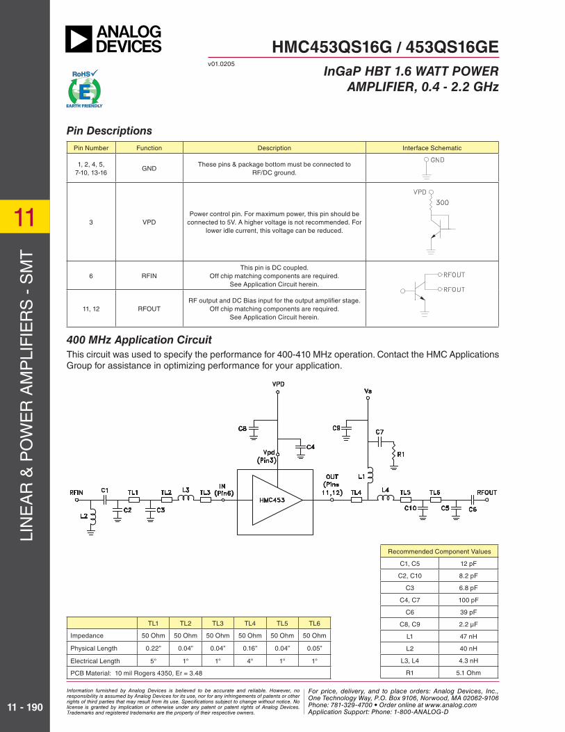
Pin Descriptions
Pin Number Function Description Interface Schematic
1, 2, 4, 5, 7-10, 13-16
GNDThese pins & package bottom must be connected to
RF/DC ground.
3 VPDPower control pin. For maximum power, this pin should be
connected to 5V. A higher voltage is not recommended. For lower idle current, this voltage can be reduced.
6 RFINThis pin is DC coupled.
Off chip matching components are required. See Application Circuit herein.
11, 12 RFOUTRF output and DC Bias input for the output amplifi er stage.
Off chip matching components are required. See Application Circuit herein.
400 MHz Application Circuit
Recommended Component Values
C1, C5 12 pF
C2, C10 8.2 pF
C3 6.8 pF
C4, C7 100 pF
C6 39 pF
C8, C9 2.2 μF
L1 47 nH
L2 40 nH
L3, L4 4.3 nH
R1 5.1 Ohm
TL1 TL2 TL3 TL4 TL5 TL6
Impedance 50 Ohm 50 Ohm 50 Ohm 50 Ohm 50 Ohm 50 Ohm
Physical Length 0.22” 0.04” 0.04” 0.16” 0.04” 0.05”
Electrical Length 5° 1° 1° 4° 1° 1°
PCB Material: 10 mil Rogers 4350, Er = 3.48
This circuit was used to specify the performance for 400-410 MHz operation. Contact the HMC Applications Group for assistance in optimizing performance for your application.
HMC453QS16G / 453QS16GEv01.0205
InGaP HBT 1.6 WATT POWER
AMPLIFIER, 0.4 - 2.2 GHz
Information furnished by Analog Devices is believed to be accurate and reliable. However, no responsibility is assumed by Analog Devices for its use, nor for any infringements of patents or other rights of third parties that may result from its use. Specifications subject to change without notice. No license is granted by implication or otherwise under any patent or patent rights of Analog Devices. Trademarks and registered trademarks are the property of their respective owners.
For price, delivery, and to place orders: Analog Devices, Inc., One Technology Way, P.O. Box 9106, Norwood, MA 02062-9106 Phone: 781-329-4700 • Order online at www.analog.com Application Support: Phone: 1-800-ANALOG-D
For price, delivery, and to place orders, please contact Hittite Microwave Corporation:20 Alpha Road, Chelmsford, MA 01824 Phone: 978-250-3343 Fax: 978-250-3373
Order On-line at www.hittite.com
LIN
EA
R &
PO
WE
R A
MP
LIF
IER
S -
SM
T
11
11 - 191
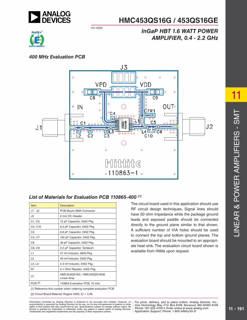
400 MHz Evaluation PCB
The circuit board used in this application should use RF circuit design techniques. Signal lines should have 50 ohm impedance while the package ground leads and exposed paddle should be connected directly to the ground plane similar to that shown. A sufficient number of VIA holes should be used to connect the top and bottom ground planes. The evaluation board should be mounted to an appropri-ate heat sink. The evaluation circuit board shown is available from Hittite upon request.
List of Materials for Evaluation PCB 110865-400 [1]
Item Description
J1 - J2 PCB Mount SMA Connector
J3 2 mm DC Header
C1, C5 12 pF Capacitor, 0402 Pkg.
C2, C10 8.2 pF Capacitor, 0402 Pkg.
C3 6.8 pF Capacitor, 0402 Pkg.
C4, C7 100 pF Capacitor, 0402 Pkg.
C6 39 pF Capacitor, 0402 Pkg.
C8, C9 2.2 μF Capacitor, Tantalum
L1 47 nH Inductor, 0603 Pkg.
L2 40 nH Inductor, 0402 Pkg.
L3, L4 4.3 nH Inductor, 0402 Pkg.
R1 5.1 Ohm Resistor, 0402 Pkg.
U1HMC453QS16G / HMC453QS16GE Linear Amp
PCB [2] 110863 Evaluation PCB, 10 mils
[1] Reference this number when ordering complete evaluation PCB
[2] Circuit Board Material: Rogers 4350, Er = 3.48
HMC453QS16G / 453QS16GEv01.0205
InGaP HBT 1.6 WATT POWER
AMPLIFIER, 0.4 - 2.2 GHz
Information furnished by Analog Devices is believed to be accurate and reliable. However, no responsibility is assumed by Analog Devices for its use, nor for any infringements of patents or other rights of third parties that may result from its use. Specifications subject to change without notice. No license is granted by implication or otherwise under any patent or patent rights of Analog Devices. Trademarks and registered trademarks are the property of their respective owners.
For price, delivery, and to place orders: Analog Devices, Inc., One Technology Way, P.O. Box 9106, Norwood, MA 02062-9106 Phone: 781-329-4700 • Order online at www.analog.com Application Support: Phone: 1-800-ANALOG-D
For price, delivery, and to place orders, please contact Hittite Microwave Corporation:20 Alpha Road, Chelmsford, MA 01824 Phone: 978-250-3343 Fax: 978-250-3373
Order On-line at www.hittite.com
11
11 - 192
LIN
EA
R &
PO
WE
R A
MP
LIF
IER
S -
SM
T
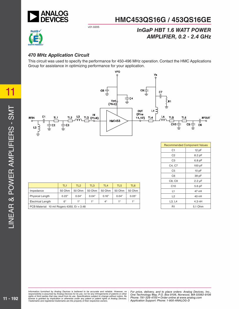
470 MHz Application Circuit
Recommended Component Values
C1 12 pF
C2 8.2 pF
C3 6.8 pF
C4, C7 100 pF
C5 10 pF
C6 39 pF
C8, C9 2.2 μF
C10 5.6 pF
L1 47 nH
L2 40 nH
L3, L4 4.3 nH
R1 5.1 Ohm
TL1 TL2 TL3 TL4 TL5 TL6
Impedance 50 Ohm 50 Ohm 50 Ohm 50 Ohm 50 Ohm 50 Ohm
Physical Length 0.22” 0.04” 0.04” 0.16” 0.04” 0.05”
Electrical Length 6° 1° 1° 4° 1° 1°
PCB Material: 10 mil Rogers 4350, Er = 3.48
This circuit was used to specify the performance for 450-496 MHz operation. Contact the HMC Applications Group for assistance in optimizing performance for your application.
HMC453QS16G / 453QS16GEInGaP HBT 1.6 WATT POWER
AMPLIFIER, 0.2 - 2.4 GHz
v01.0205
Information furnished by Analog Devices is believed to be accurate and reliable. However, no responsibility is assumed by Analog Devices for its use, nor for any infringements of patents or other rights of third parties that may result from its use. Specifications subject to change without notice. No license is granted by implication or otherwise under any patent or patent rights of Analog Devices. Trademarks and registered trademarks are the property of their respective owners.
For price, delivery, and to place orders: Analog Devices, Inc., One Technology Way, P.O. Box 9106, Norwood, MA 02062-9106 Phone: 781-329-4700 • Order online at www.analog.com Application Support: Phone: 1-800-ANALOG-D
For price, delivery, and to place orders, please contact Hittite Microwave Corporation:20 Alpha Road, Chelmsford, MA 01824 Phone: 978-250-3343 Fax: 978-250-3373
Order On-line at www.hittite.com
LIN
EA
R &
PO
WE
R A
MP
LIF
IER
S -
SM
T
11
11 - 193
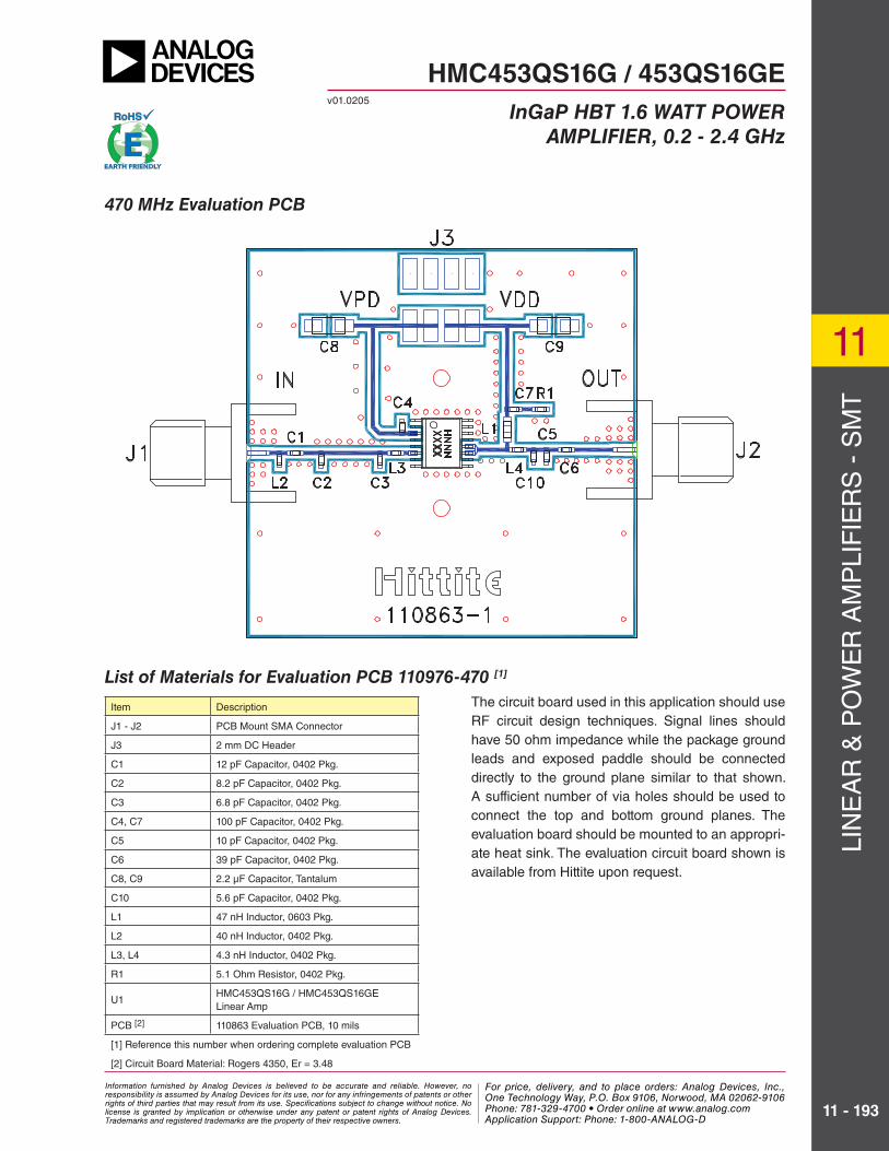
470 MHz Evaluation PCB
The circuit board used in this application should use RF circuit design techniques. Signal lines should have 50 ohm impedance while the package ground leads and exposed paddle should be connected directly to the ground plane similar to that shown. A sufficient number of via holes should be used to connect the top and bottom ground planes. The evaluation board should be mounted to an appropri-ate heat sink. The evaluation circuit board shown is available from Hittite upon request.
List of Materials for Evaluation PCB 110976-470 [1]
Item Description
J1 - J2 PCB Mount SMA Connector
J3 2 mm DC Header
C1 12 pF Capacitor, 0402 Pkg.
C2 8.2 pF Capacitor, 0402 Pkg.
C3 6.8 pF Capacitor, 0402 Pkg.
C4, C7 100 pF Capacitor, 0402 Pkg.
C5 10 pF Capacitor, 0402 Pkg.
C6 39 pF Capacitor, 0402 Pkg.
C8, C9 2.2 μF Capacitor, Tantalum
C10 5.6 pF Capacitor, 0402 Pkg.
L1 47 nH Inductor, 0603 Pkg.
L2 40 nH Inductor, 0402 Pkg.
L3, L4 4.3 nH Inductor, 0402 Pkg.
R1 5.1 Ohm Resistor, 0402 Pkg.
U1HMC453QS16G / HMC453QS16GELinear Amp
PCB [2] 110863 Evaluation PCB, 10 mils
[1] Reference this number when ordering complete evaluation PCB
[2] Circuit Board Material: Rogers 4350, Er = 3.48
HMC453QS16G / 453QS16GEInGaP HBT 1.6 WATT POWER
AMPLIFIER, 0.2 - 2.4 GHz
v01.0205
Information furnished by Analog Devices is believed to be accurate and reliable. However, no responsibility is assumed by Analog Devices for its use, nor for any infringements of patents or other rights of third parties that may result from its use. Specifications subject to change without notice. No license is granted by implication or otherwise under any patent or patent rights of Analog Devices. Trademarks and registered trademarks are the property of their respective owners.
For price, delivery, and to place orders: Analog Devices, Inc., One Technology Way, P.O. Box 9106, Norwood, MA 02062-9106 Phone: 781-329-4700 • Order online at www.analog.com Application Support: Phone: 1-800-ANALOG-D
For price, delivery, and to place orders, please contact Hittite Microwave Corporation:20 Alpha Road, Chelmsford, MA 01824 Phone: 978-250-3343 Fax: 978-250-3373
Order On-line at www.hittite.com
11
11 - 194
LIN
EA
R &
PO
WE
R A
MP
LIF
IER
S -
SM
T
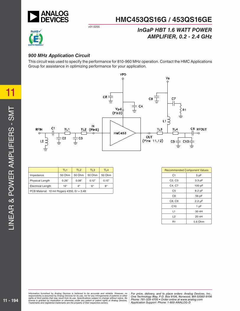
900 MHz Application Circuit
This circuit was used to specify the performance for 810-960 MHz operation. Contact the HMC Applications Group for assistance in optimizing performance for your application.
Recommended Component Values
C1 5 pF
C2, C3 3.3 pF
C4, C7 100 pF
C5 8.2 pF
C6 56 pF
C8, C9 2.2 μF
C10 1 pF
L1 30 nH
L2 20 nH
R1 5.6 Ohm
TL1 TL2 TL3 TL4
Impedance 50 Ohm 50 Ohm 50 Ohm 50 Ohm
Physical Length 0.26” 0.08” 0.12” 0.15”
Electrical Length 14° 4° 6° 8°
PCB Material: 10 mil Rogers 4350, Er = 3.48
HMC453QS16G / 453QS16GEInGaP HBT 1.6 WATT POWER
AMPLIFIER, 0.2 - 2.4 GHz
v01.0205
Information furnished by Analog Devices is believed to be accurate and reliable. However, no responsibility is assumed by Analog Devices for its use, nor for any infringements of patents or other rights of third parties that may result from its use. Specifications subject to change without notice. No license is granted by implication or otherwise under any patent or patent rights of Analog Devices. Trademarks and registered trademarks are the property of their respective owners.
For price, delivery, and to place orders: Analog Devices, Inc., One Technology Way, P.O. Box 9106, Norwood, MA 02062-9106 Phone: 781-329-4700 • Order online at www.analog.com Application Support: Phone: 1-800-ANALOG-D
For price, delivery, and to place orders, please contact Hittite Microwave Corporation:20 Alpha Road, Chelmsford, MA 01824 Phone: 978-250-3343 Fax: 978-250-3373
Order On-line at www.hittite.com
LIN
EA
R &
PO
WE
R A
MP
LIF
IER
S -
SM
T
11
11 - 195
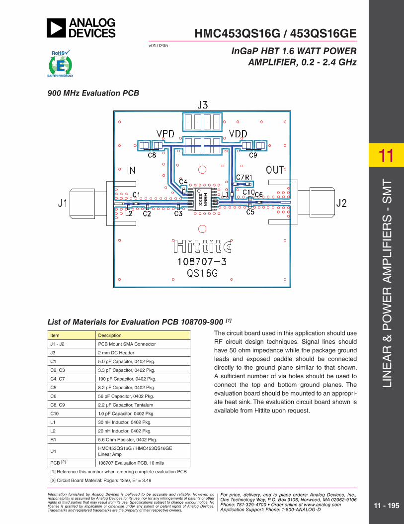
900 MHz Evaluation PCB
The circuit board used in this application should use RF circuit design techniques. Signal lines should have 50 ohm impedance while the package ground leads and exposed paddle should be connected directly to the ground plane similar to that shown. A sufficient number of via holes should be used to connect the top and bottom ground planes. The evaluation board should be mounted to an appropri-ate heat sink. The evaluation circuit board shown is available from Hittite upon request.
List of Materials for Evaluation PCB 108709-900 [1]
Item Description
J1 - J2 PCB Mount SMA Connector
J3 2 mm DC Header
C1 5.0 pF Capacitor, 0402 Pkg.
C2, C3 3.3 pF Capacitor, 0402 Pkg.
C4, C7 100 pF Capacitor, 0402 Pkg.
C5 8.2 pF Capacitor, 0402 Pkg.
C6 56 pF Capacitor, 0402 Pkg.
C8, C9 2.2 μF Capacitor, Tantalum
C10 1.0 pF Capacitor, 0402 Pkg.
L1 30 nH Inductor, 0402 Pkg.
L2 20 nH Inductor, 0402 Pkg.
R1 5.6 Ohm Resistor, 0402 Pkg.
U1HMC453QS16G / HMC453QS16GELinear Amp
PCB [2] 108707 Evaluation PCB, 10 mils
[1] Reference this number when ordering complete evaluation PCB
[2] Circuit Board Material: Rogers 4350, Er = 3.48
HMC453QS16G / 453QS16GEInGaP HBT 1.6 WATT POWER
AMPLIFIER, 0.2 - 2.4 GHz
v01.0205
Information furnished by Analog Devices is believed to be accurate and reliable. However, no responsibility is assumed by Analog Devices for its use, nor for any infringements of patents or other rights of third parties that may result from its use. Specifications subject to change without notice. No license is granted by implication or otherwise under any patent or patent rights of Analog Devices. Trademarks and registered trademarks are the property of their respective owners.
For price, delivery, and to place orders: Analog Devices, Inc., One Technology Way, P.O. Box 9106, Norwood, MA 02062-9106 Phone: 781-329-4700 • Order online at www.analog.com Application Support: Phone: 1-800-ANALOG-D
For price, delivery, and to place orders, please contact Hittite Microwave Corporation:20 Alpha Road, Chelmsford, MA 01824 Phone: 978-250-3343 Fax: 978-250-3373
Order On-line at www.hittite.com
11
11 - 196
LIN
EA
R &
PO
WE
R A
MP
LIF
IER
S -
SM
T
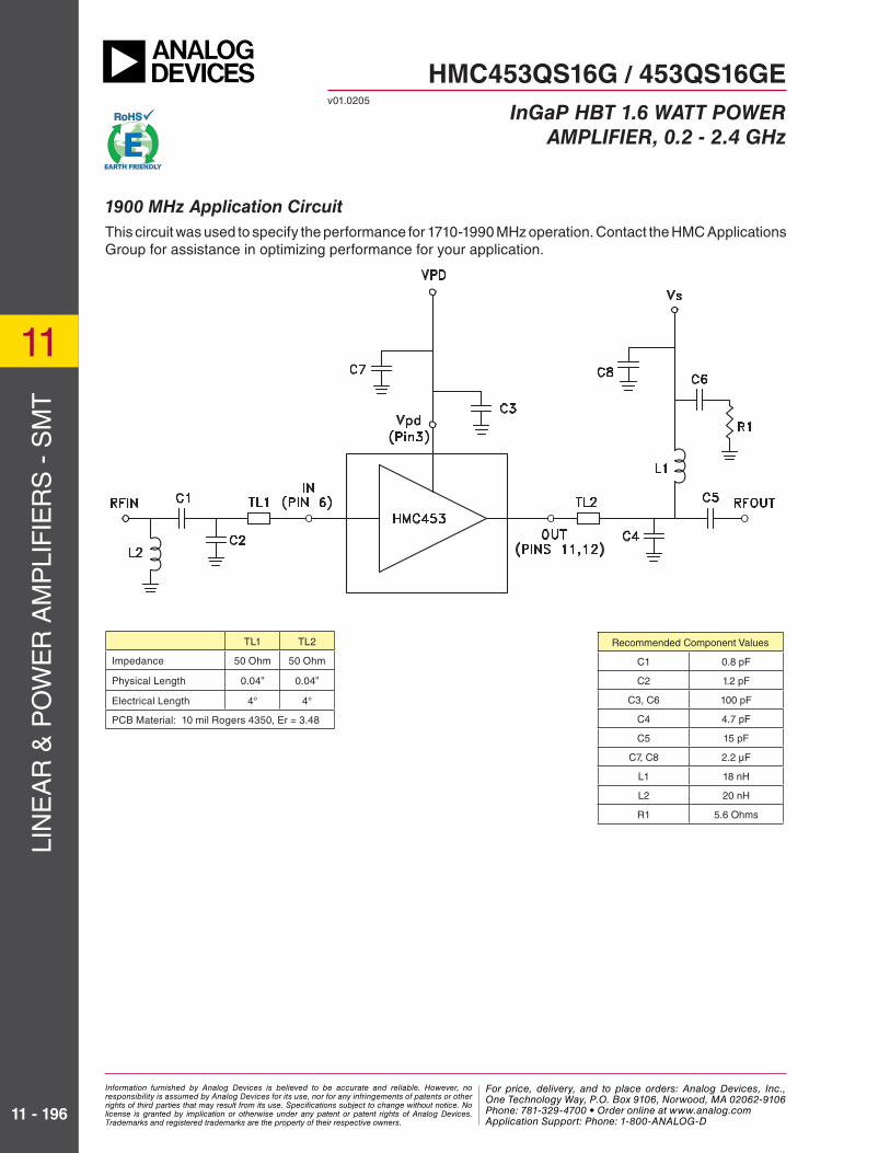
1900 MHz Application Circuit
Recommended Component Values
C1 0.8 pF
C2 1.2 pF
C3, C6 100 pF
C4 4.7 pF
C5 15 pF
C7, C8 2.2 μF
L1 18 nH
L2 20 nH
R1 5.6 Ohms
This circuit was used to specify the performance for 1710-1990 MHz operation. Contact the HMC Applications Group for assistance in optimizing performance for your application.
TL1 TL2
Impedance 50 Ohm 50 Ohm
Physical Length 0.04” 0.04”
Electrical Length 4° 4°
PCB Material: 10 mil Rogers 4350, Er = 3.48
HMC453QS16G / 453QS16GEInGaP HBT 1.6 WATT POWER
AMPLIFIER, 0.2 - 2.4 GHz
v01.0205
Information furnished by Analog Devices is believed to be accurate and reliable. However, no responsibility is assumed by Analog Devices for its use, nor for any infringements of patents or other rights of third parties that may result from its use. Specifications subject to change without notice. No license is granted by implication or otherwise under any patent or patent rights of Analog Devices. Trademarks and registered trademarks are the property of their respective owners.
For price, delivery, and to place orders: Analog Devices, Inc., One Technology Way, P.O. Box 9106, Norwood, MA 02062-9106 Phone: 781-329-4700 • Order online at www.analog.com Application Support: Phone: 1-800-ANALOG-D
For price, delivery, and to place orders, please contact Hittite Microwave Corporation:20 Alpha Road, Chelmsford, MA 01824 Phone: 978-250-3343 Fax: 978-250-3373
Order On-line at www.hittite.com
LIN
EA
R &
PO
WE
R A
MP
LIF
IER
S -
SM
T
11
11 - 197
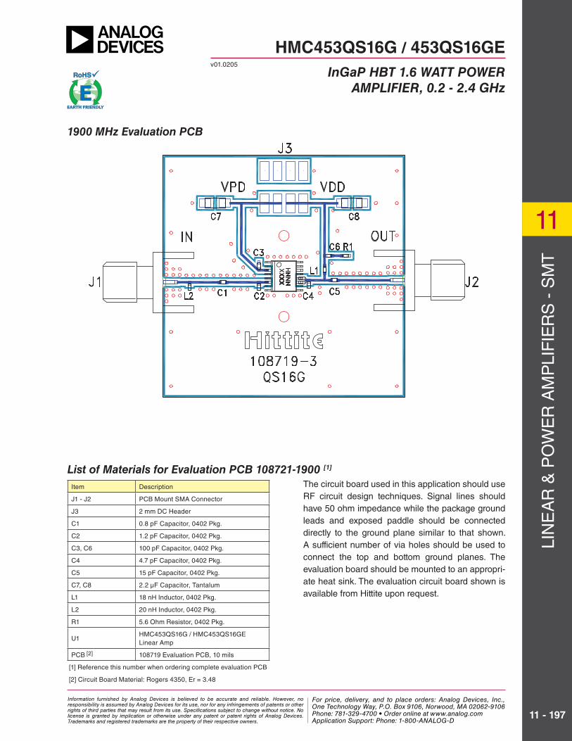
1900 MHz Evaluation PCB
The circuit board used in this application should use RF circuit design techniques. Signal lines should have 50 ohm impedance while the package ground leads and exposed paddle should be connected directly to the ground plane similar to that shown. A sufficient number of via holes should be used to connect the top and bottom ground planes. The evaluation board should be mounted to an appropri-ate heat sink. The evaluation circuit board shown is available from Hittite upon request.
List of Materials for Evaluation PCB 108721-1900 [1]
Item Description
J1 - J2 PCB Mount SMA Connector
J3 2 mm DC Header
C1 0.8 pF Capacitor, 0402 Pkg.
C2 1.2 pF Capacitor, 0402 Pkg.
C3, C6 100 pF Capacitor, 0402 Pkg.
C4 4.7 pF Capacitor, 0402 Pkg.
C5 15 pF Capacitor, 0402 Pkg.
C7, C8 2.2 μF Capacitor, Tantalum
L1 18 nH Inductor, 0402 Pkg.
L2 20 nH Inductor, 0402 Pkg.
R1 5.6 Ohm Resistor, 0402 Pkg.
U1HMC453QS16G / HMC453QS16GELinear Amp
PCB [2] 108719 Evaluation PCB, 10 mils
[1] Reference this number when ordering complete evaluation PCB
[2] Circuit Board Material: Rogers 4350, Er = 3.48
HMC453QS16G / 453QS16GEInGaP HBT 1.6 WATT POWER
AMPLIFIER, 0.2 - 2.4 GHz
v01.0205
Information furnished by Analog Devices is believed to be accurate and reliable. However, no responsibility is assumed by Analog Devices for its use, nor for any infringements of patents or other rights of third parties that may result from its use. Specifications subject to change without notice. No license is granted by implication or otherwise under any patent or patent rights of Analog Devices. Trademarks and registered trademarks are the property of their respective owners.
For price, delivery, and to place orders: Analog Devices, Inc., One Technology Way, P.O. Box 9106, Norwood, MA 02062-9106 Phone: 781-329-4700 • Order online at www.analog.com Application Support: Phone: 1-800-ANALOG-D
For price, delivery, and to place orders, please contact Hittite Microwave Corporation:20 Alpha Road, Chelmsford, MA 01824 Phone: 978-250-3343 Fax: 978-250-3373
Order On-line at www.hittite.com
11
11 - 198
LIN
EA
R &
PO
WE
R A
MP
LIF
IER
S -
SM
T
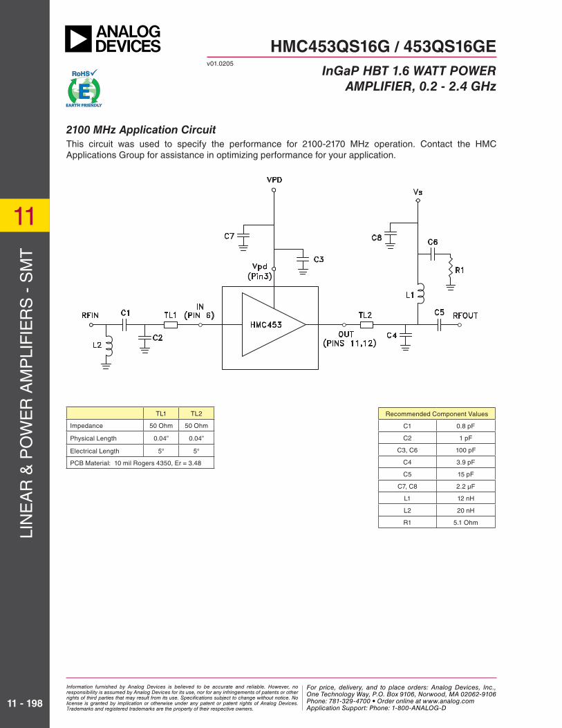
2100 MHz Application Circuit
This circuit was used to specify the performance for 2100-2170 MHz operation. Contact the HMC Applications Group for assistance in optimizing performance for your application.
Recommended Component Values
C1 0.8 pF
C2 1 pF
C3, C6 100 pF
C4 3.9 pF
C5 15 pF
C7, C8 2.2 μF
L1 12 nH
L2 20 nH
R1 5.1 Ohm
TL1 TL2
Impedance 50 Ohm 50 Ohm
Physical Length 0.04” 0.04”
Electrical Length 5° 5°
PCB Material: 10 mil Rogers 4350, Er = 3.48
HMC453QS16G / 453QS16GEInGaP HBT 1.6 WATT POWER
AMPLIFIER, 0.2 - 2.4 GHz
v01.0205
Information furnished by Analog Devices is believed to be accurate and reliable. However, no responsibility is assumed by Analog Devices for its use, nor for any infringements of patents or other rights of third parties that may result from its use. Specifications subject to change without notice. No license is granted by implication or otherwise under any patent or patent rights of Analog Devices. Trademarks and registered trademarks are the property of their respective owners.
For price, delivery, and to place orders: Analog Devices, Inc., One Technology Way, P.O. Box 9106, Norwood, MA 02062-9106 Phone: 781-329-4700 • Order online at www.analog.com Application Support: Phone: 1-800-ANALOG-D

For price, delivery, and to place orders, please contact Hittite Microwave Corporation:20 Alpha Road, Chelmsford, MA 01824 Phone: 978-250-3343 Fax: 978-250-3373
Order On-line at www.hittite.com
LIN
EA
R &
PO
WE
R A
MP
LIF
IER
S -
SM
T
11
11 - 199
2100 MHz Evaluation PCB
The circuit board used in this application should use RF circuit design techniques. Signal lines should have 50 ohm impedance while the package ground leads and exposed paddle should be connected directly to the ground plane similar to that shown. A sufficient number of via holes should be used to connect the top and bottom ground planes. The evaluation board should be mounted to an appropri-ate heat sink. The evaluation circuit board shown is available from Hittite upon request.
List of Materials for Evaluation PCB 109994-2100 [1]
Item Description
J1 - J2 PCB Mount SMA Connector
J3 2 mm DC Header
C1 0.8 pF Capacitor, 0402 Pkg.
C2 1.0 pF Capacitor, 0402 Pkg.
C3, C6 100 pF Capacitor, 0402 Pkg.
C4 3.9 pF Capacitor, 0402 Pkg.
C5 15 pF Capacitor, 0402 Pkg.
C7, C8 2.2 μF Capacitor, Tantalum
L1 12 nH Inductor, 0402 Pkg.
L2 20 nH Inductor, 0402 Pkg.
R1 5.1 Ohm Resistor, 0402 Pkg.
U1HMC453QS16G / HMC453QS16GE Linear Amp
PCB [2] 108719 Evaluation PCB, 10 mils
[1] Reference this number when ordering complete evaluation PCB
[2] Circuit Board Material: Rogers 4350, Er = 3.48
HMC453QS16G / 453QS16GEInGaP HBT 1.6 WATT POWER
AMPLIFIER, 0.2 - 2.4 GHz
v01.0205
Information furnished by Analog Devices is believed to be accurate and reliable. However, no responsibility is assumed by Analog Devices for its use, nor for any infringements of patents or other rights of third parties that may result from its use. Specifications subject to change without notice. No license is granted by implication or otherwise under any patent or patent rights of Analog Devices. Trademarks and registered trademarks are the property of their respective owners.
For price, delivery, and to place orders: Analog Devices, Inc., One Technology Way, P.O. Box 9106, Norwood, MA 02062-9106 Phone: 781-329-4700 • Order online at www.analog.com Application Support: Phone: 1-800-ANALOG-D
Related Documents