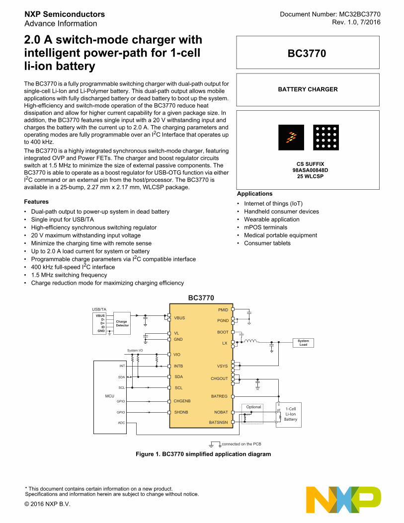
Document Number: MC32BC3770 Rev. 1.0, 7/2016 NXP Semiconductors Advance Information * This document contains certain information on a new product. Specifications and information herein are subject to change without notice. © 2016 NXP B.V. 2.0 A switch-mode charger with intelligent power-path for 1-cell li-ion battery The BC3770 is a fully programmable switching charger with dual-path output for single-cell Li-Ion and Li-Polymer battery. This dual-path output allows mobile applications with fully discharged battery or dead battery to boot up the system. High-efficiency and switch-mode operation of the BC3770 reduce heat dissipation and allow for higher current capability for a given package size. In addition, the BC3770 features single input with a 20 V withstanding input and charges the battery with the current up to 2.0 A. The charging parameters and operating modes are fully programmable over an I 2 C Interface that operates up to 400 kHz. The BC3770 is a highly integrated synchronous switch-mode charger, featuring integrated OVP and Power FETs. The charger and boost regulator circuits switch at 1.5 MHz to minimize the size of external passive components. The BC3770 is able to operate as a boost regulator for USB-OTG function via either I 2 C command or an external pin from the host/processor. The BC3770 is available in a 25-bump, 2.27 mm x 2.17 mm, WLCSP package. Features • Dual-path output to power-up system in dead battery • Single input for USB/TA • High-efficiency synchronous switching regulator • 20 V maximum withstanding input voltage • Minimize the charging time with remote sense • Up to 2.0 A load current for system or battery • Programmable charge parameters via I 2 C compatible interface • 400 kHz full-speed I 2 C interface • 1.5 MHz switching frequency • Charge reduction mode for maximizing charging efficiency Figure 1. BC3770 simplified application diagram BATTERY CHARGER BC3770 CS SUFFIX 98ASA00848D 25 WLCSP Applications • Internet of things (IoT) • Handheld consumer devices • Wearable application • mPOS terminals • Medical portable equipment • Consumer tablets LX PGND System I/O GND System Load PMID BOOT VBUS D- D+ ID GND USB/TA NOBAT SDA SCL INTB INT SDA SCL MCU CHGENB VSYS GPIO BATSNSN VL SHDNB CHGOUT BATREG GPIO VIO connected on the PCB ADC Optional BC3770 Charge Detector + - VF 1-Cell Li-Ion Battery VBUS

Welcome message from author
This document is posted to help you gain knowledge. Please leave a comment to let me know what you think about it! Share it to your friends and learn new things together.
Transcript
Document Number: MC32BC3770Rev. 1.0, 7/2016
NXP Semiconductors Advance Information
* This document contains certain information on a new product. Specifications and information herein are subject to change without notice.
© 2016 NXP B.V.
2.0 A switch-mode charger with intelligent power-path for 1-cell li-ion batteryThe BC3770 is a fully programmable switching charger with dual-path output for single-cell Li-Ion and Li-Polymer battery. This dual-path output allows mobile applications with fully discharged battery or dead battery to boot up the system. High-efficiency and switch-mode operation of the BC3770 reduce heat dissipation and allow for higher current capability for a given package size. In addition, the BC3770 features single input with a 20 V withstanding input and charges the battery with the current up to 2.0 A. The charging parameters and operating modes are fully programmable over an I2C Interface that operates up to 400 kHz.
The BC3770 is a highly integrated synchronous switch-mode charger, featuring integrated OVP and Power FETs. The charger and boost regulator circuits switch at 1.5 MHz to minimize the size of external passive components. The BC3770 is able to operate as a boost regulator for USB-OTG function via either I2C command or an external pin from the host/processor. The BC3770 is available in a 25-bump, 2.27 mm x 2.17 mm, WLCSP package.
Features
• Dual-path output to power-up system in dead battery• Single input for USB/TA• High-efficiency synchronous switching regulator• 20 V maximum withstanding input voltage • Minimize the charging time with remote sense• Up to 2.0 A load current for system or battery• Programmable charge parameters via I2C compatible interface• 400 kHz full-speed I2C interface• 1.5 MHz switching frequency• Charge reduction mode for maximizing charging efficiency
Figure 1. BC3770 simplified application diagram
BATTERY CHARGER
BC3770
CS SUFFIX98ASA00848D
25 WLCSP
Applications
• Internet of things (IoT)• Handheld consumer devices• Wearable application• mPOS terminals• Medical portable equipment• Consumer tablets
LX
PGND
System I/O
GND SystemLoad
PMID
BOOT
VBUSD-D+ID
GND
USB/TA
NOBAT
SDA
SCL
INTBINT
SDA
SCL
MCUCHGENB
VSYS
GPIO
BATSNSN
VL
SHDNB
CHGOUT
BATREG
GPIO
VIO
connected on the PCB
ADC
Optional
BC3770
ChargeDetector
+
-
VF 1-CellLi-IonBattery
VBUS
NXP Semiconductors 2
BC3770
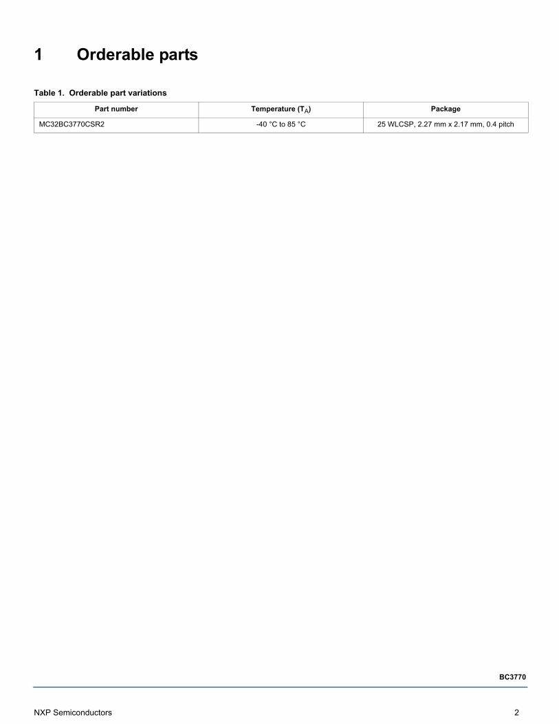
1 Orderable parts
Table 1. Orderable part variations
Part number Temperature (TA) Package
MC32BC3770CSR2 -40 °C to 85 °C 25 WLCSP, 2.27 mm x 2.17 mm, 0.4 pitch
3 NXP Semiconductors
BC3770
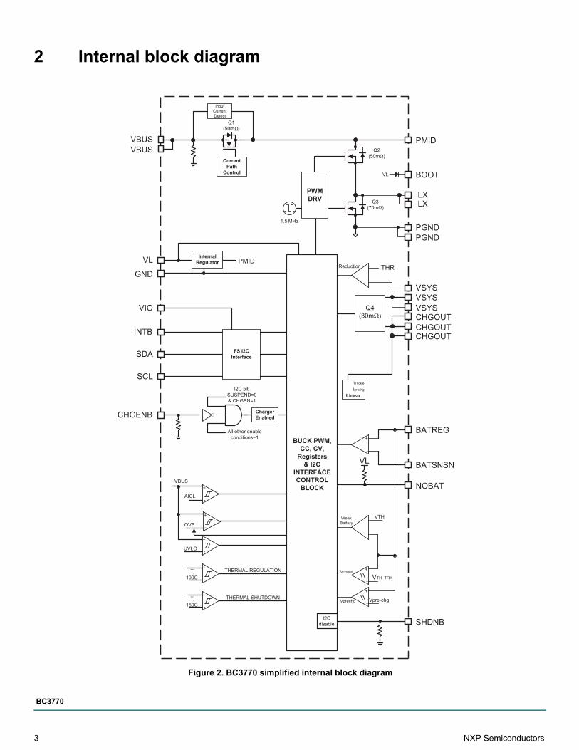
2 Internal block diagram
Figure 2. BC3770 simplified internal block diagram
VBUS
LX
CurrentPath
Control
150CTj
PGND
BUCK PWM,CC, CV,
Registers& I2C
INTERFACECONTROL
BLOCKAICL
OVP
UVLO
+
-
+
-
+
-
THERMAL SHUTDOWN
GND
PWMDRV
VBUS
VTH
+
-
VTrickle
VTH_TRK
WeakBattery
PMID
BOOT
+
-Vprechg Vpre-chg
InputCurrentDetect
Linear
ITrickle
Iprechg
Q1(50mΩ)
Q2(50mΩ)
Q3(70m )
NOBAT
+
-
SDA
SCL
INTB
FS I2CInterface
VL
CHGENB
VSYS
1.5 MHz
VL
All other enable conditions=1
ChargerEnabled
I2C bit,SUSPEND=0& CHGEN=1
BATSNSN
VL InternalRegulator PMID
+
-
Q4(30mΩ)
THRReduction
100CTj
+
-
THERMAL REGULATION
SHDNB
CHGOUT
BATREG
I2Cdisable
VIO
LX
PGND
VSYS
VSYS
CHGOUTCHGOUT
VBUS
Ω
NXP Semiconductors 4
BC3770
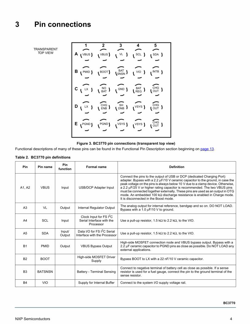
3 Pin connections
Figure 3. BC3770 pin connections (transparent top view)
Functional descriptions of many of these pins can be found in the Functional Pin Description section beginning on page 13.
Table 2. BC3770 pin definitions
Pin Pin namePin
functionFormal name Definition
A1, A2 VBUS Input USB/DCP Adapter Input
Connect the pins to the output of USB or DCP (dedicated Charging Port) adapter. Bypass with a 2.2 μF/10 V ceramic capacitor to the ground, in case the peak voltage on the pins is always below 10 V due to a clamp device. Otherwise, a 2.2 μF/25 V or higher rating capacitor is recommended. The two VBUS pins must be connected together externally. These pins are used as an output in OTG mode. An embedded 100 kΩ discharge resistance is enabled in Charge mode. It is disconnected in the Boost mode.
A3 VL Output Internal Regulator OutputThe analog output for internal reference, bandgap and so on. DO NOT LOAD. Bypass with a 1.0 μF/10 V to ground.
A4 SCL Input Clock Input for FS I2C Serial Interface with the
ProcessorUse a pull-up resistor, 1.5 kΩ to 2.2 kΩ, to the VIO.
A5 SDAInput/Output
Data I/O for FS I2C Serial Interface with the Processor
Use a pull-up resistor, 1.5 kΩ to 2.2 kΩ, to the VIO.
B1 PMID Output VBUS Bypass OutputHigh-side MOSFET connection node and VBUS bypass output. Bypass with a 2.2 μF ceramic capacitor to PGND pins as close as possible. Do NOT LOAD any external applications.
B2 BOOTHigh-side MOSFET Driver
SupplyBypass BOOT to LX with a 22 nF/10 V ceramic capacitor.
B3 BATSNSN Battery - Terminal SensingConnect to negative terminal of battery cell as close as possible. If a sense resistor is used for a fuel gauge, connect the pin to the ground terminal of the sense resistor.
B4 VIO Supply for Internal Buffer Connect to the system I/O supply voltage rail.
TRANSPARENTTOP VIEW A
B
C
D
E
1 2 3 4 5
VBUS
PMID
LX
LX
PGND
VBUS
BOOT
NO
CHG
PGND
BAT
ENB
VL
BAT
GND
SH
VSYS
SNSN
DNB
SCL
VIO
BAT
VSYS
VSYS
REG
SDA
INTB
CHGOUT
CHGOUT
CHGOUT
5 NXP Semiconductors
BC3770
B5 INTB Output Logic Output for InterruptAn open-drain output with an external pull-up resistor, 200 kΩ, to the system I/O supply. Active-low when status change on interrupt registers occurs.
C1, D1 LX Switching NodeConnect a 1.0 μH inductor. The two LX pins must be connected together externally.
C2 NOBAT InputLogic Input for Battery Presence Detection
Connect the pin to VF or ID pin on the battery cell. It has an internal pull-up resistance, 300 kΩ typ, to the VL. If a logic-high threshold is detected on the pin, the charging is suspended immediately. If this pin is not used, connect it to ground.
C3 GND Ground Device Ground Must be connected to the system ground.
C4 BATREG Battery + Terminal Sensing Connect to positive terminal of battery cell as close as possible.
C5, D5, E5 CHGOUT Output Battery Charger OutputThese pins must be connected together externally. Bypass with a 4.7 μF/10 V or higher to ground.
D2 CHGENB Input Charger Enable Logic Input
Logic-low to enable charger. Logic-high to disable the charger, not to disable buck converter. It has an internal 300 kΩ resistance to ground. If this pin is not used, leave it open or connect it to ground. The serial interface, I2C, is still available in CHGENB = High.
D3 SHDNB InputLogic Input for Disabling I2C
Interface
If there is no valid input source, logic-low is to put the I2C interface into Disabled mode to reduce the idle current as low as possible. In the Shutdown mode, I2C interface is not available but the Q4 FET is kept ON. A valid power source on VBUS is able to overwrite to wake-up the device for Charge mode even in SHDNB = Low. This pin is not effective as long as a valid input power source is present. This pin has an internal pull-down resistance, 300 kΩ typ. If this pin is not used, tie it to the system I/O supply rail or an appropriate rail to reduce idle current as low as possible.
D4, E3, E4 VSYS Output System Supply Output
VSYS is the power supply for the system load. When a valid power source at VBUS is attached, VSYS is regulated at 3.6 V until the BATREG hits the threshold of VSYS_MIN x RDS(on)_Q4. When the +Terminal on the battery cell is regulated at VBATREG, the VSYS output is regulated to the IFAST_CHG x RDS(on)_Q4 above BATREG. Bypass with a 10 μF/10 V ceramic capacitor to ground.
E1, E2 PGND GroundPower Ground for the Buck
ConverterThe two PGND pins must be connected together externally.
Table 2. BC3770 pin definitions (continued)
Pin Pin namePin
functionFormal name Definition
NXP Semiconductors 6
BC3770
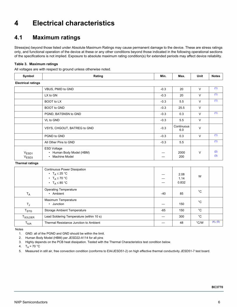
4 Electrical characteristics
4.1 Maximum ratings
Stress(es) beyond those listed under Absolute Maximum Ratings may cause permanent damage to the device. These are stress ratings only, and functional operation of the device at these or any other conditions beyond those indicated in the following operational sections of the specifications is not implied. Exposure to absolute maximum rating condition(s) for extended periods may affect device reliability.
Table 3. Maximum ratings
All voltages are with respect to ground unless otherwise noted.
Symbol Rating Min. Max. Unit Notes
Electrical ratings
VBUS, PMID to GND -0.3 20 V (1)
LX to GN -0.3 20 V (1)
BOOT to LX - 0.3 5.5 V (1)
BOOT to GND - 0.3 25.5 V
PGND, BATSNSN to GND - 0.3 0.3 V (1)
VL to GND - 0.3 5.5 V
VSYS, CHGOUT, BATREG to GND - 0.3Continuous
6.0V
PGND to GND - 0.3 0.3 V (1)
All Other Pins to GND - 0.3 5.5 (1)
VESD1VESD3
ESD Voltage• Human Body Model (HBM)• Machine Model
——
2000200
V (2)
(3)
Thermal ratings
Continuous Power Dissipation• TA ≤ 25 °C
• TA ≤ 70 °C
• TA ≤ 85 °C
———
2.081.14
0.832
W
TA
Operating Temperature • Ambient - 40 85
°C
TJ
Maximum Temperature • Junction — 150
°C
TSTG Storage Ambient Temperature -65 150 °C
TSOLDER Lead Soldering Temperature (within 10 s) — 300 °C
TθJA Thermal Resistance Junction to Ambient — 48 °C/W (4), (5)
Notes1. GND: all of the PGND and GND should be within the limit.2. Human Body Model (HBM) per JESD22-A114 for all pins3. Highly depends on the PCB heat dissipation. Tested with the Thermal Characteristics test condition below.4. TA = 70 °C
5. Measured in still air, free convection condition (conforms to EIA/JESD51-2) on high effective thermal conductivity JESD51-7 test board.
7 NXP Semiconductors
BC3770
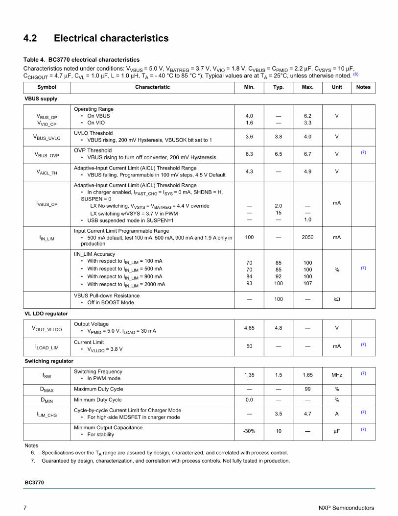
4.2 Electrical characteristics
Table 4. BC3770 electrical characteristics
Characteristics noted under conditions: VVBUS = 5.0 V, VBATREG = 3.7 V, VVIO = 1.8 V, CVBUS = CPMID = 2.2 μF, CVSYS = 10 μF, CCHGOUT = 4.7 μF, CVL = 1.0 μF, L = 1.0 μH, TA = - 40 °C to 85 °C *). Typical values are at TA = 25°C, unless otherwise noted. (6)
Symbol Characteristic Min. Typ. Max. Unit Notes
VBUS supply
VBUS_OPVVIO_OP
Operating Range• On VBUS• On VIO
4.01.6
——
6.23.3
V
VBUS_UVLOUVLO Threshold
• VBUS rising, 200 mV Hysteresis, VBUSOK bit set to 13.6 3.8 4.0 V
VBUS_OVPOVP Threshold
• VBUS rising to turn off converter, 200 mV Hysteresis6.3 6.5 6.7 V (7)
VAICL_THAdaptive-Input Current Limit (AICL) Threshold Range
• VBUS falling, Programmable in 100 mV steps, 4.5 V Default4.3 — 4.9 V
IVBUS_OP
Adaptive-Input Current Limit (AICL) Threshold Range• In charger enabled, IFAST_CHG = ISYS = 0 mA, SHDNB = H, SUSPEN = 0
LX No switching, VVSYS = VBATREG = 4.4 V override
LX switching w/VSYS = 3.7 V in PWM• USB suspended mode in SUSPEN=1
———
2.015—
——1.0
mA
IIN_LIM
Input Current Limit Programmable Range• 500 mA default, test 100 mA, 500 mA, 900 mA and 1.9 A only in production
100 — 2050 mA
IIN_LIM Accuracy• With respect to IIN_LIM = 100 mA
• With respect to IIN_LIM = 500 mA
• With respect to IIN_LIM = 900 mA
• With respect to IIN_LIM = 2000 mA
70708493
858592
100
100100100107
% (7)
VBUS Pull-down Resistance• Off in BOOST Mode
— 100 — kΩ
VL LDO regulator
VOUT_VLLDOOutput Voltage
• VPMID = 5.0 V, ILOAD = 30 mA4.65 4.8 — V
ILOAD_LIMCurrent Limit
• VVLLDO = 3.8 V50 — — mA (7)
Switching regulator
fSWSwitching Frequency
• In PWM mode1.35 1.5 1.65 MHz (7)
DMAX Maximum Duty Cycle — — 99 %
DMIN Minimum Duty Cycle 0.0 — — %
ILIM_CHGCycle-by-cycle Current Limit for Charger Mode
• For high-side MOSFET in charger mode— 3.5 4.7 A (7)
Minimum Output Capacitance• For stability
-30% 10 — μF (7)
Notes6. Specifications over the TA range are assured by design, characterized, and correlated with process control.
7. Guaranteed by design, characterization, and correlation with process controls. Not fully tested in production.
NXP Semiconductors 8
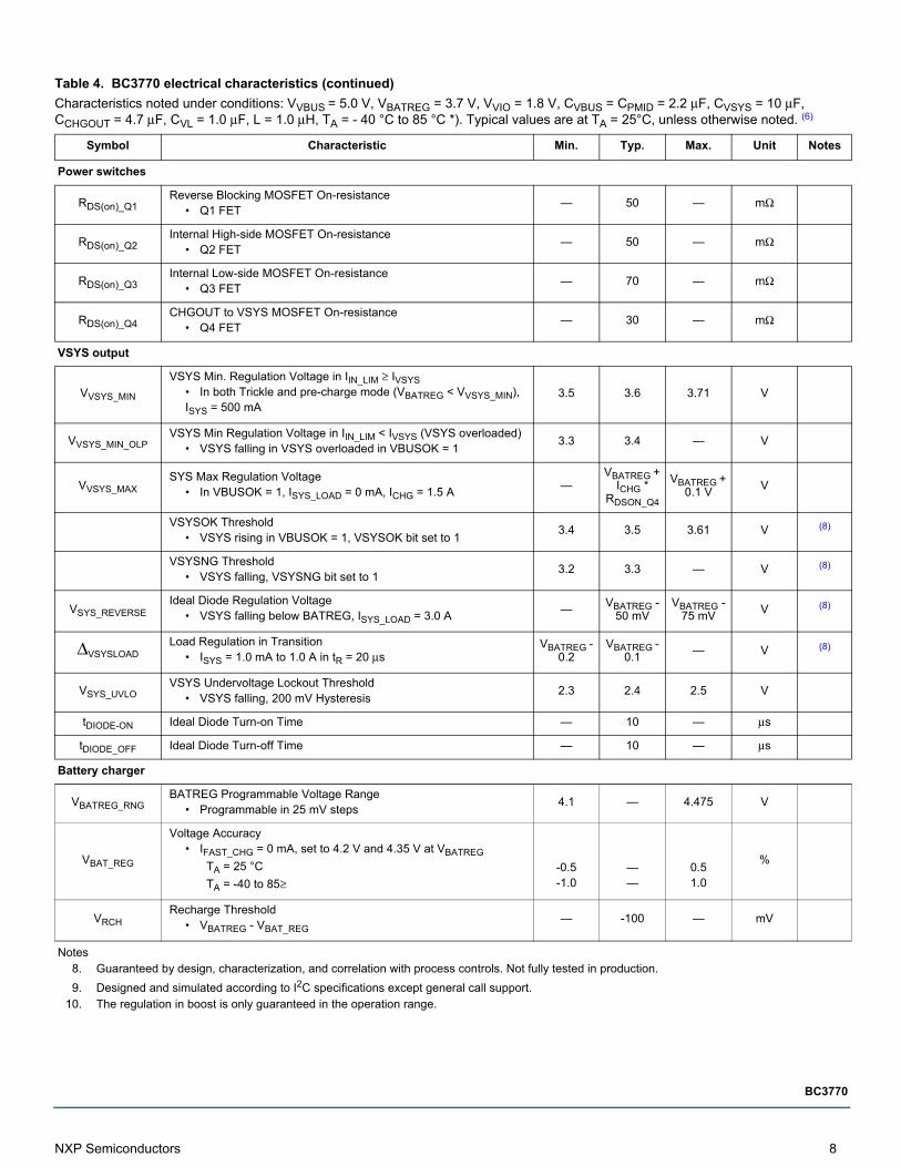
BC3770
Power switches
RDS(on)_Q1Reverse Blocking MOSFET On-resistance
• Q1 FET— 50 — mΩ
RDS(on)_Q2Internal High-side MOSFET On-resistance
• Q2 FET— 50 — mΩ
RDS(on)_Q3Internal Low-side MOSFET On-resistance
• Q3 FET— 70 — mΩ
RDS(on)_Q4CHGOUT to VSYS MOSFET On-resistance
• Q4 FET— 30 — mΩ
VSYS output
VVSYS_MIN
VSYS Min. Regulation Voltage in IIN_LIM ≥ IVSYS• In both Trickle and pre-charge mode (VBATREG < VVSYS_MIN), ISYS = 500 mA
3.5 3.6 3.71 V
VVSYS_MIN_OLPVSYS Min Regulation Voltage in IIN_LIM < IVSYS (VSYS overloaded)
• VSYS falling in VSYS overloaded in VBUSOK = 13.3 3.4 — V
VVSYS_MAXSYS Max Regulation Voltage
• In VBUSOK = 1, ISYS_LOAD = 0 mA, ICHG = 1.5 A—
VBATREG + ICHG *
RDSON_Q4
VBATREG + 0.1 V
V
VSYSOK Threshold• VSYS rising in VBUSOK = 1, VSYSOK bit set to 1
3.4 3.5 3.61 V (8)
VSYSNG Threshold• VSYS falling, VSYSNG bit set to 1
3.2 3.3 — V (8)
VSYS_REVERSEIdeal Diode Regulation Voltage
• VSYS falling below BATREG, ISYS_LOAD = 3.0 A—
VBATREG -50 mV
VBATREG -75 mV
V (8)
ΔVSYSLOADLoad Regulation in Transition
• ISYS = 1.0 mA to 1.0 A in tR = 20 μsVBATREG -
0.2VBATREG -
0.1— V (8)
VSYS_UVLOVSYS Undervoltage Lockout Threshold
• VSYS falling, 200 mV Hysteresis2.3 2.4 2.5 V
tDIODE-ON Ideal Diode Turn-on Time — 10 — μs
tDIODE_OFF Ideal Diode Turn-off Time — 10 — μs
Battery charger
VBATREG_RNGBATREG Programmable Voltage Range
• Programmable in 25 mV steps4.1 — 4.475 V
VBAT_REG
Voltage Accuracy• IFAST_CHG = 0 mA, set to 4.2 V and 4.35 V at VBATREG
TA = 25 °C
TA = -40 to 85≥-0.5-1.0
——
0.51.0
%
VRCHRecharge Threshold
• VBATREG - VBAT_REG— -100 — mV
Notes8. Guaranteed by design, characterization, and correlation with process controls. Not fully tested in production.
9. Designed and simulated according to I2C specifications except general call support.10. The regulation in boost is only guaranteed in the operation range.
Table 4. BC3770 electrical characteristics (continued)
Characteristics noted under conditions: VVBUS = 5.0 V, VBATREG = 3.7 V, VVIO = 1.8 V, CVBUS = CPMID = 2.2 μF, CVSYS = 10 μF, CCHGOUT = 4.7 μF, CVL = 1.0 μF, L = 1.0 μH, TA = - 40 °C to 85 °C *). Typical values are at TA = 25°C, unless otherwise noted. (6)
Symbol Characteristic Min. Typ. Max. Unit Notes
9 NXP Semiconductors
BC3770
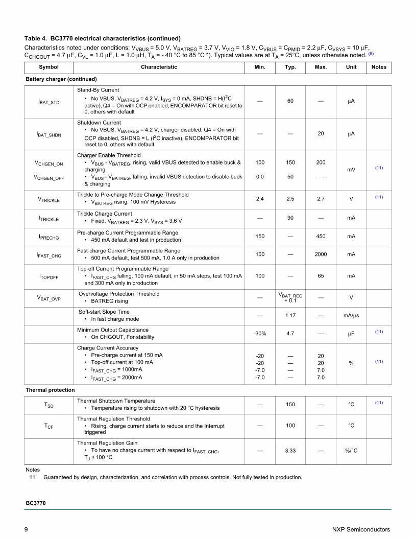
Battery charger (continued)
IBAT_STD
Stand-By Current
• No VBUS, VBATREG = 4.2 V, ISYS = 0 mA, SHDNB = H(I2C active), Q4 = On with OCP enabled, ENCOMPARATOR bit reset to 0, others with default
— 60 — μA
IBAT_SHDN
Shutdown Current• No VBUS, VBATREG = 4.2 V, charger disabled, Q4 = On with
OCP disabled, SHDNB = L (I2C inactive), ENCOMPARATOR bit reset to 0, others with default
— — 20 μA
VCHGEN_ON
VCHGEN_OFF
Charger Enable Threshold• VBUS - VBATREG, rising, valid VBUS detected to enable buck & charging• VBUS - VBATREG, falling, invalid VBUS detection to disable buck & charging
100
0.0
150
50
200
—mV (11)
VTRICKLETrickle to Pre-charge Mode Change Threshold
• VBATREG rising, 100 mV Hysteresis2.4 2.5 2.7 V (11)
ITRICKLETrickle Charge Current
• Fixed, VBATREG = 2.3 V, VSYS = 3.6 V— 90 — mA
IPRECHGPre-charge Current Programmable Range
• 450 mA default and test in production150 — 450 mA
IFAST_CHGFast-charge Current Programmable Range
• 500 mA default, test 500 mA, 1.0 A only in production100 — 2000 mA
ITOPOFF
Top-off Current Programmable Range• IFAST_CHG falling, 100 mA default, in 50 mA steps, test 100 mA and 300 mA only in production
100 — 65 mA
VBAT_OVP Overvoltage Protection Threshold
• BATREG rising—
VBAT_REG + 0.1
— V
Soft-start Slope Time• In fast charge mode
— 1.17 — mA/μs
Minimum Output Capacitance• On CHGOUT, For stability
-30% 4.7 — μF (11)
Charge Current Accuracy• Pre-charge current at 150 mA• Top-off current at 100 mA• IFAST_CHG = 1000mA
• IFAST_CHG = 2000mA
-20-20-7.0-7.0
————
20207.07.0
% (11)
Thermal protection
TSDThermal Shutdown Temperature
• Temperature rising to shutdown with 20 °C hysteresis— 150 — °C (11)
TCF
Thermal Regulation Threshold• Rising, charge current starts to reduce and the Interrupt triggered
— 100 — °C
Thermal Regulation Gain• To have no charge current with respect to IFAST_CHG, TJ ≥ 100 °C
— 3.33 — %/°C
Notes11. Guaranteed by design, characterization, and correlation with process controls. Not fully tested in production.
Table 4. BC3770 electrical characteristics (continued)
Characteristics noted under conditions: VVBUS = 5.0 V, VBATREG = 3.7 V, VVIO = 1.8 V, CVBUS = CPMID = 2.2 μF, CVSYS = 10 μF, CCHGOUT = 4.7 μF, CVL = 1.0 μF, L = 1.0 μH, TA = - 40 °C to 85 °C *). Typical values are at TA = 25°C, unless otherwise noted. (6)
Symbol Characteristic Min. Typ. Max. Unit Notes
NXP Semiconductors 10
BC3770
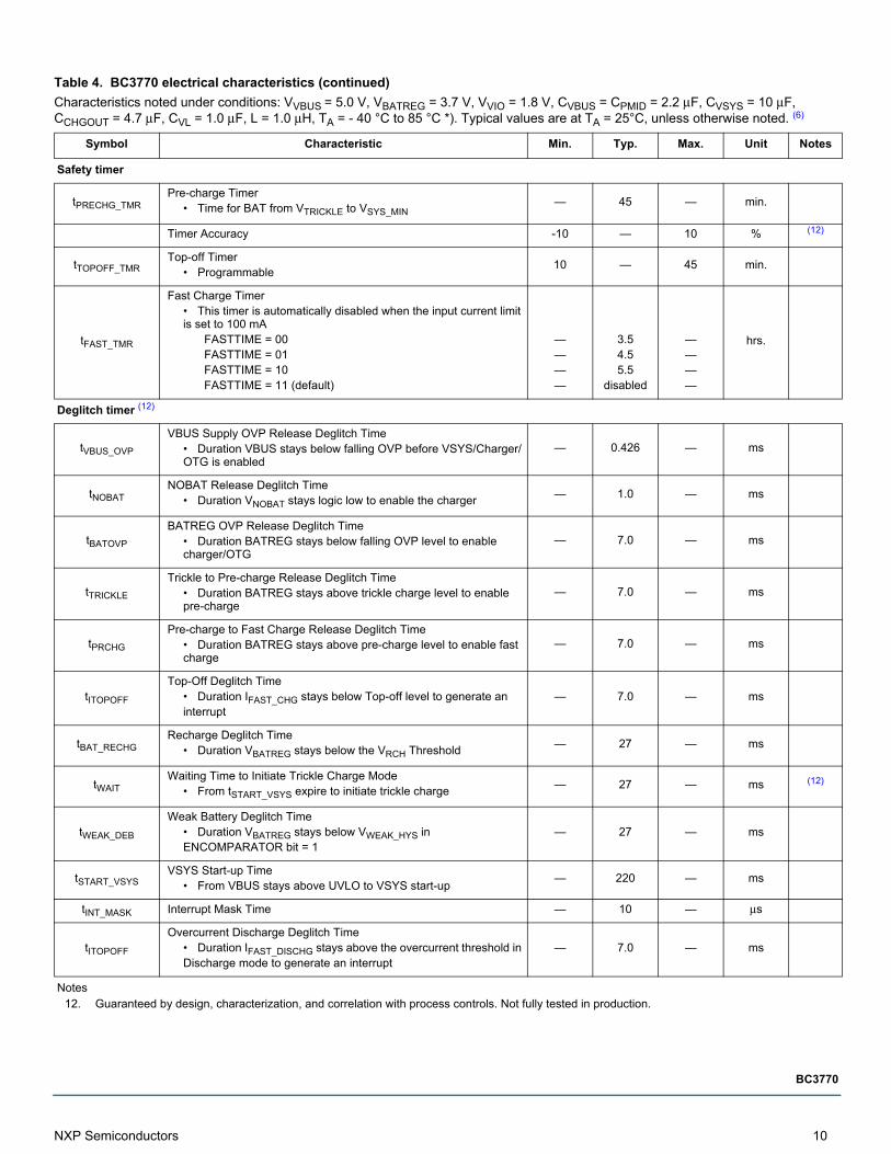
Safety timer
tPRECHG_TMRPre-charge Timer
• Time for BAT from VTRICKLE to VSYS_MIN— 45 — min.
Timer Accuracy -10 — 10 % (12)
tTOPOFF_TMRTop-off Timer
• Programmable10 — 45 min.
tFAST_TMR
Fast Charge Timer• This timer is automatically disabled when the input current limit is set to 100 mA
FASTTIME = 00FASTTIME = 01FASTTIME = 10FASTTIME = 11 (default)
————
3.54.55.5
disabled
————
hrs.
Deglitch timer (12)
tVBUS_OVP
VBUS Supply OVP Release Deglitch Time• Duration VBUS stays below falling OVP before VSYS/Charger/OTG is enabled
— 0.426 — ms
tNOBATNOBAT Release Deglitch Time
• Duration VNOBAT stays logic low to enable the charger— 1.0 — ms
tBATOVP
BATREG OVP Release Deglitch Time• Duration BATREG stays below falling OVP level to enable charger/OTG
— 7.0 — ms
tTRICKLE
Trickle to Pre-charge Release Deglitch Time• Duration BATREG stays above trickle charge level to enable pre-charge
— 7.0 — ms
tPRCHG
Pre-charge to Fast Charge Release Deglitch Time• Duration BATREG stays above pre-charge level to enable fast charge
— 7.0 — ms
tITOPOFF
Top-Off Deglitch Time• Duration IFAST_CHG stays below Top-off level to generate an interrupt
— 7.0 — ms
tBAT_RECHGRecharge Deglitch Time
• Duration VBATREG stays below the VRCH Threshold— 27 — ms
tWAITWaiting Time to Initiate Trickle Charge Mode
• From tSTART_VSYS expire to initiate trickle charge— 27 — ms (12)
tWEAK_DEB
Weak Battery Deglitch Time• Duration VBATREG stays below VWEAK_HYS in ENCOMPARATOR bit = 1
— 27 — ms
tSTART_VSYSVSYS Start-up Time
• From VBUS stays above UVLO to VSYS start-up— 220 — ms
tINT_MASK Interrupt Mask Time — 10 — μs
tITOPOFF
Overcurrent Discharge Deglitch Time• Duration IFAST_DISCHG stays above the overcurrent threshold in Discharge mode to generate an interrupt
— 7.0 — ms
Notes12. Guaranteed by design, characterization, and correlation with process controls. Not fully tested in production.
Table 4. BC3770 electrical characteristics (continued)
Characteristics noted under conditions: VVBUS = 5.0 V, VBATREG = 3.7 V, VVIO = 1.8 V, CVBUS = CPMID = 2.2 μF, CVSYS = 10 μF, CCHGOUT = 4.7 μF, CVL = 1.0 μF, L = 1.0 μH, TA = - 40 °C to 85 °C *). Typical values are at TA = 25°C, unless otherwise noted. (6)
Symbol Characteristic Min. Typ. Max. Unit Notes
11 NXP Semiconductors
BC3770
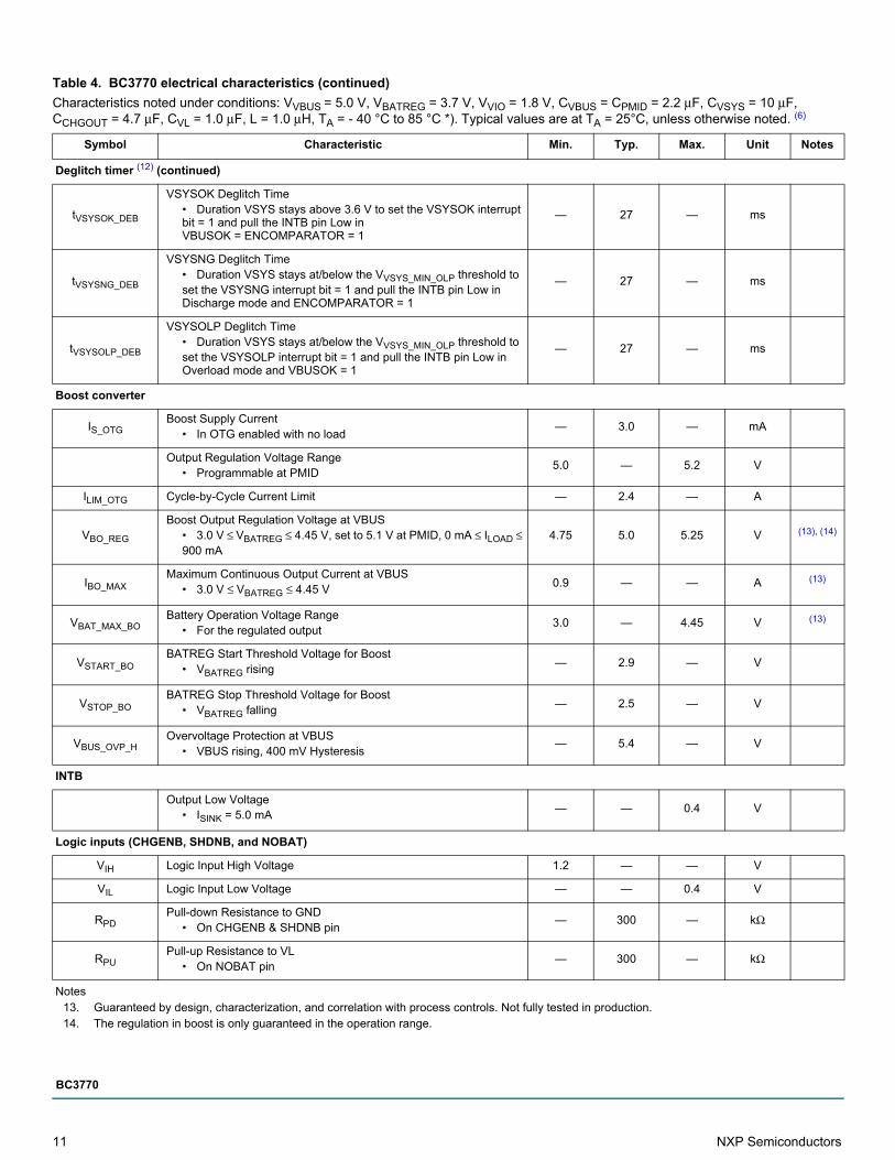
Deglitch timer (12) (continued)
tVSYSOK_DEB
VSYSOK Deglitch Time• Duration VSYS stays above 3.6 V to set the VSYSOK interrupt bit = 1 and pull the INTB pin Low in VBUSOK = ENCOMPARATOR = 1
— 27 — ms
tVSYSNG_DEB
VSYSNG Deglitch Time• Duration VSYS stays at/below the VVSYS_MIN_OLP threshold to set the VSYSNG interrupt bit = 1 and pull the INTB pin Low in Discharge mode and ENCOMPARATOR = 1
— 27 — ms
tVSYSOLP_DEB
VSYSOLP Deglitch Time• Duration VSYS stays at/below the VVSYS_MIN_OLP threshold to set the VSYSOLP interrupt bit = 1 and pull the INTB pin Low in Overload mode and VBUSOK = 1
— 27 — ms
Boost converter
IS_OTGBoost Supply Current
• In OTG enabled with no load— 3.0 — mA
Output Regulation Voltage Range• Programmable at PMID
5.0 — 5.2 V
ILIM_OTG Cycle-by-Cycle Current Limit — 2.4 — A
VBO_REG
Boost Output Regulation Voltage at VBUS• 3.0 V ≤ VBATREG ≤ 4.45 V, set to 5.1 V at PMID, 0 mA ≤ ILOAD ≤ 900 mA
4.75 5.0 5.25 V (13), (14)
IBO_MAXMaximum Continuous Output Current at VBUS
• 3.0 V ≤ VBATREG ≤ 4.45 V0.9 — — A (13)
VBAT_MAX_BOBattery Operation Voltage Range
• For the regulated output3.0 — 4.45 V (13)
VSTART_BOBATREG Start Threshold Voltage for Boost
• VBATREG rising— 2.9 — V
VSTOP_BOBATREG Stop Threshold Voltage for Boost
• VBATREG falling— 2.5 — V
VBUS_OVP_HOvervoltage Protection at VBUS
• VBUS rising, 400 mV Hysteresis— 5.4 — V
INTB
Output Low Voltage• ISINK = 5.0 mA
— — 0.4 V
Logic inputs (CHGENB, SHDNB, and NOBAT)
VIH Logic Input High Voltage 1.2 — — V
VIL Logic Input Low Voltage — — 0.4 V
RPDPull-down Resistance to GND
• On CHGENB & SHDNB pin— 300 — kΩ
RPUPull-up Resistance to VL
• On NOBAT pin— 300 — kΩ
Notes13. Guaranteed by design, characterization, and correlation with process controls. Not fully tested in production.14. The regulation in boost is only guaranteed in the operation range.
Table 4. BC3770 electrical characteristics (continued)
Characteristics noted under conditions: VVBUS = 5.0 V, VBATREG = 3.7 V, VVIO = 1.8 V, CVBUS = CPMID = 2.2 μF, CVSYS = 10 μF, CCHGOUT = 4.7 μF, CVL = 1.0 μF, L = 1.0 μH, TA = - 40 °C to 85 °C *). Typical values are at TA = 25°C, unless otherwise noted. (6)
Symbol Characteristic Min. Typ. Max. Unit Notes
NXP Semiconductors 12
BC3770
Weak battery detection
VWEAK_LWeak Battery Programmable Range
• BATREG falling, programmable in 50 mV steps3.0 — 3.75 V
Weak Battery Threshold Accuracy -5.0 — 0.4 % (15)
VWEAK_HYSWeak Battery Voltage Hysteresis
• BATREG rising— 100 — mV
I2C interface (15), (16)
VIH_I2CI2C Logic Input High Threshold Voltage
• SDA, SCL1.2 — — V
VIL_I2CI2C Logic Input Low Threshold Voltage
• SDA, SCL— — 0.4 V
VOL_I2CI2C Logic Output Low Voltage
• SDA at 3.0 mA sink current— — 0.4 V
fSCL SCL Clock Frequency 0.0 — 400 kHz
Notes15. Guaranteed by design, characterization, and correlation with process controls. Not fully tested in production.16. The regulation in boost is only guaranteed in the operation range.
Table 4. BC3770 electrical characteristics (continued)
Characteristics noted under conditions: VVBUS = 5.0 V, VBATREG = 3.7 V, VVIO = 1.8 V, CVBUS = CPMID = 2.2 μF, CVSYS = 10 μF, CCHGOUT = 4.7 μF, CVL = 1.0 μF, L = 1.0 μH, TA = - 40 °C to 85 °C *). Typical values are at TA = 25°C, unless otherwise noted. (6)
Symbol Characteristic Min. Typ. Max. Unit Notes
13 NXP Semiconductors
BC3770
5 Functional device operation
5.1 Introduction
The BC3770 is a fully programmable switching charger with a single-input for USB/DCP adapter and a dual-path output for single-cell Li-Ion and Li-Polymer batteries. The dual-path output allows mobile applications with a fully discharged or dead battery to boot up the system through the VSYS output. High-efficiency and switch-mode operation of the BC3770 reduce thermal dissipation and allows the battery to charge faster with a higher current capability. The BC3770 supports single input up to 20 V max. absolute voltage and charges the battery with the current up to 2.0 A. Owing to a high-efficiency in a wide range of input voltages and charging currents, the switch mode charger is a good choice for fast charging with less power loss and better thermal management than a linear charger. The charging parameters and operating modes are fully programmable over an I2C interface that operates up to 400 kHz in full speed. The BC3770 features a highly integrated synchronous switch-mode charger, intelligent power-path, VSYS stable control scheme in overload condition, and an automatic battery detection function. The charger and boost regulator circuit switches at 1.5 MHz, to minimize the size of external passive components.
To ensure USB compliance and minimize charging time, the input current is able to be limited to the value set through the I2C. The setting of charge top-off current is also programmable over I2C.
The BC3770 provides battery charging in four modes: trickle, pre-charge, fast charge (constant current), and full-charge (constant voltage). The charging restart circuit automatically restarts the fast-charge cycle in full-charge mode when the battery falls below an internal threshold over the deglitch time and detected top-off threshold. Input and charge status are reported to the processors through the interrupt pin, INTB. Charge current is reduced when the die temperature reaches 100 °C, while the system current is maintained. The BC3770 is able to operate as a boost regulator for USB-OTG devices over I2C.
5.2 Features
• Dual-path output to power-up system in dead battery• Single Input for USB/TA• High-efficiency synchronous switching regulator• 20 V maximum withstanding input voltage • Minimize the charging time with remote sense• Up to 2.0 A load current for system or battery• Programmable charge parameters via I2C compatible interface
• Fast charge current• Charge termination current• Battery regulation voltage• Pre-charge current• Fast charge threshold voltage• Charge reduction threshold voltage
• 400 kHz full-speed I2C interface• 1.5 MHz switching frequency• Charge reduction mode for maximizing charging efficiency• Protection
• Thermal protection• Thermal regulation• Input/output overvoltage protection• Adaptive input current limit protection (AICL)• Reverse leakage protection• No battery detection over pin detection• Battery OVP protection• Overcurrent protection in discharge mode
• Boost mode operation for USB OTG• Output voltage: 5.0 V to 5.2 V, programmable at 900 mA
NXP Semiconductors 14
BC3770
5.3 Operational modes
5.3.1 Undervoltage lockout (UVLO)The BC3770 has a typical undervoltage lockout threshold of 3.8 V, with a 200 mV hysteresis, rising on VBUS. VSYS also has a falling 2.5 V typical with 200 mV hysteresis. When the input supply voltage is below the 3.6 V typical UVLO falling level, the PWM buck converter turns off.
5.3.2 Registers resetAll programmable registers in the device are reset to the default values when the following condition is met.
• Reset Condition: VSYS ≤ VSYS_UVLO
5.3.3 Q4 FET on in no valid VBUSIf the battery is connected with the voltage above a typical of 2.4 V and no any valid input power source is attached, the Q4 FET between VSYS and CHGOUT turns On and connects the Battery to the system, regardless of status of SHDNB. The VL regulator stays off.
5.3.4 Charge modeThe BC3770 performs the following pre-qualification process before initiating the Charging mode:
1. Input Voltage: Detect the validation of VBUS power source, charger enable threshold, and Adaptive-Input Current Limit (AICL) threshold. If the falling VBUS hits the AICL threshold, the charging current is reduced to limit the amount of drop on VBUS power source. In addition, the device senses the input voltage is at least above BATREG + 150 mV.
2. Battery Presence Detection: Detect the status of battery presence through the NOBAT pin. If the voltage on the NOBAT pin is above the logic high threshold, the charging is suspended (Internal Q4 FET is open). However, VSYS is regulated at VVSYS_MAX as long as a valid input source is attached.
3. Battery Voltage: Sense the battery voltage if it is less than the BAT OVP threshold.
4. Die Temperature: If the die temperature is above 130 °C or less than 150 °C, charging is suspended.
5. Overvoltage Detection (OVP): Sense if the VBUS is less than the OVP threshold. If the OVP condition is detected, the PWM converter is immediately shut off.
6. Validation of Software and Hardware Enable signals: Detect the status of software enable bit, CHGEN=1, SUSPEN=0, and hardware pin of CHGENB=LOW.
This pre-qualification process is continuously monitored and charging is suspended until all conditions are met.
5.3.5 Charging profile
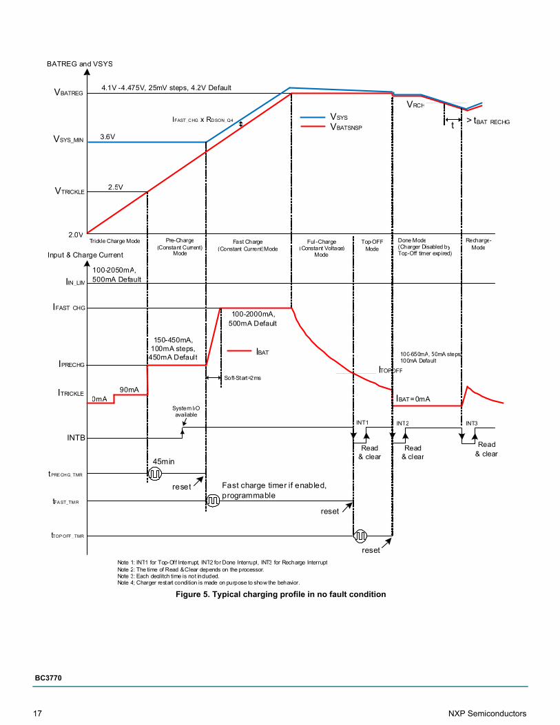
5.3.5.1 Trickle-charge mode
Trickle-charge mode is automatically enabled in 27 ms after the VSYS start-up time expires. The battery is charged with a fixed 90 mA charge current until the battery voltage reaches the threshold, 2.5 V typical in rising. This threshold is not programmable over I2C. As soon as the battery voltage crosses over the threshold, a pre-charge mode is activated automatically after the fixed deglitch time. This allows the protection circuit in the battery pack to be reset with no damage, and brings the battery voltage to a higher level.
5.3.5.2 Pre-charge mode
The Pre-charge mode is enabled in tTRICKLE when the battery voltage crosses over a typical 2.5 V. The safety timer called pre-charge timer, tPRECHG_TMR, 45-minute counts at the same time as well. This timer is reset as soon as the Fast-charge mode is initiated. This allows a deeply discharged battery to charge safely. The pre-charge current is programmable from 150 mA to 450 mA in 100 mA steps over I2C. If the battery voltage does not exceed the VVSYS_MIN threshold before the timer expires, charging is suspended and a fault signal is asserted via the INTB pin. If the VSYS voltage drops due to the limited input power source during the mode, the charge current is automatically reduce to maintain the VSYS as low as at 3.4 V. If the load is still overloaded, even in no charge current and limited input current, the VSYS can't help the collapse.
15 NXP Semiconductors
BC3770
5.3.5.3 Fast-charge mode (constant-current mode)
The Fast-charge mode is entered in tPRECHG when the battery voltage exceeds the VVSYS_MIN threshold of a typical 3.6 V. During this mode, the battery is charged with a programmable fast-charge current. The fast-charge current is programmable from 100 mA to 2000 mA with a 500 mA default. Fast-charge current is always limited by the input current limit setting. As soon as the battery voltage reaches the VVSYS_MIN threshold, VSYS tracks the battery voltage through the Q4. This is called 'tracking mode”. In tracking mode, power dissipation is minimized by RDSON_Q4 x IFAST_CHG. However, if the VSYS voltage drops during the fast-charge mode, the charge current is automatically reduce to keep the dropout voltage, to ensure proper operation of charging circuitry. During this fast-charge mode, the safety timer called fast charge timer, tFAST_TMR, counts. If the battery voltage does not reach the VBAT_REG threshold before the timer expires, charging is suspended and a fault signal is asserted via the INTB pin. This timer is programmable and is disabled by default. This timer is automatically disabled when the input current limit is set to 100 mA.
5.3.5.4 Full-charge mode (constant-voltage mode)
As soon as the BATREG voltage reaches the VBAT_REG threshold, the fast-charge current is reduced to a programmable top-off current. The VBAT_REG regulation threshold is programmable from 4.1 V to 4.475 V in 25 mV steps.
5.3.5.5 Top-off mode (constant-voltage mode)
If the charge current down to a pre-programmed top-off current threshold is sensed over tITOPOFF, the safety timer called top-off timer, tTOPOFF_TMR, 45-minute by default, automatically counts. The top-off interrupt event is reported to the processor via the INTB. As soon as the processor reads the interrupt registers, the processor is able to turn off the charger by either CHGENB = H, CHGEN = 0, or wait until the timer expires in AUTOSTOP=1. The top-off current is programmable from 100 mA to 650 mA in 50 mA steps. 100 mA is the default.
5.3.5.6 Done mode (constant-voltage mode)
After the top-off timer expires, the charger is Off automatically in AUTOSTOP=1. However, the charger stays at CV (Constant-voltage mode) in AUTOSTOP=0 even though the top-off timer expires. The interrupt signal of Done is reported to the processors via the INTB pin, regardless of the AUTOSTOP status.
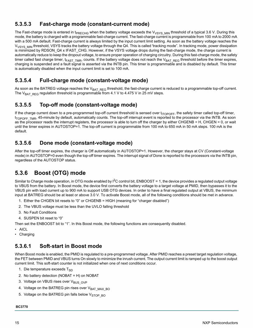
5.3.6 Boost (OTG) modeSimilar to Charge mode operation, in OTG mode enabled by I2C control bit, ENBOOST = 1, the device provides a regulated output voltage to VBUS from the battery. In Boost mode, the device first converts the battery voltage to a target voltage at PMID, then bypasses it to the VBUS pin with load current up to 900 mA to support USB OTG devices. In order to have a final regulated output at VBUS, the minimum input at BATREG should be at least or above 3.0 V. To activate Boost mode, all of the following conditions should be met in advance.
1. Either the CHGEN bit resets to “0” or CHGENB = HIGH (meaning for “charger disabled”)
2. The VBUS voltage must be less than the UVLO falling threshold
3. No Fault Conditions
4. SUSPEN bit reset to “0”
Then set the ENBOOST bit to “1”. In this Boost mode, the following functions are consequently disabled.
• AICL• Charging
5.3.6.1 Soft-start in Boost mode
When Boost mode is enabled, the PMID is regulated to a pre-programmed voltage. After PMID reaches a preset target regulation voltage, the FET between PMID and VBUS turns On slowly to minimize the inrush current. The output current limit is ramped up to the boost output current limit. This soft-start counter is not initialized when one of next conditions occur.
1. Die temperature exceeds TSD
2. No battery detection (NOBAT = H) on NOBAT
3. Voltage on VBUS rises over VBUS_OVP
4. Voltage on the BATREG pin rises over VBAT_MAX_BO
5. Voltage on the BATREG pin falls below VSTOP_BO
NXP Semiconductors 16
BC3770
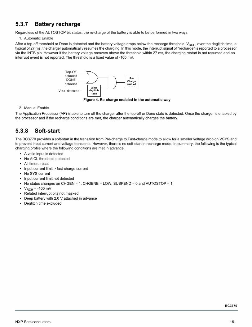
5.3.7 Battery rechargeRegardless of the AUTOSTOP bit status, the re-charge of the battery is able to be performed in two ways.
1. Automatic Enable
After a top-off threshold or Done is detected and the battery voltage drops below the recharge threshold, VRCH, over the deglitch time, a typical of 27 ms, the charger automatically resumes the charging. In this mode, the interrupt signal of “recharge” is reported to a processor via the INTB pin. However if the battery voltage recovers above the threshold within 27 ms, the charging restart is not resumed and an interrupt event is not reported. The threshold is a fixed value of -100 mV.
Figure 4. Re-charge enabled in the automatic way
2. Manual Enable
The Application Processor (AP) is able to turn off the charger after the top-off or Done state is detected. Once the charger is enabled by the processor and if the recharge conditions are met, the charger automatically charges the battery.
5.3.8 Soft-startThe BC3770 provides a soft-start in the transition from Pre-charge to Fast-charge mode to allow for a smaller voltage drop on VSYS and to prevent input current and voltage transients. However, there is no soft-start in recharge mode. In summary, the following is the typical charging profile where the following conditions are met in advance.
• A valid input is detected• No AICL threshold detected• All timers reset • Input current limit > fast-charge current • No SYS current• Input current limit not detected• No status changes on CHGEN = 1, CHGENB = LOW, SUSPEND = 0 and AUTOSTOP = 1• VRCH = -100 mV• Related interrupt bits not masked• Deep battery with 2.0 V attached in advance• Deglitch time excluded
Top-Off detected
Re-Charge enabled
VRCH detected
DONE detected
27ms deglitch
time
17 NXP Semiconductors
BC3770
Figure 5. Typical charging profile in no fault condition
BATREG and VSYS
VBATREG4.1V -4.475V , 25mV steps, 4.2V Default
VSYS_MIN 3.6V
VTRICKLE2.5V
VSYS
VBATSNSP
Trickle Charge Mode Pre-Charge (Constant Current)
Mode
Fast Charge (Constant Current) Mode
Top-OFF Mode
Done Mode(Charger Disabled by Top-Off timer expired)
ITRICKLE90mA
Soft-Start=2ms
IPRECHG
150-450mA, 100mA steps,
450mA Default
IFAST CHG
Input & Charge Current
IBAT
100-2000mA, 500mA Default
ITOPOFF
100-650mA, 50mA steps, 100mA Default
IBAT =0mA
INTBRead
& clear
Full-Charge (Constant Voltage)
Mode
Read & clear
Note 1: INT1 for Top-Off Interrupt, INT2 for Done Interrupt, INT3 for Recharge Interrupt Note 2: The time of Read & Clear depends on the processor.Note 3: Each deglitch time is not included. Note 4; Charger restart condition is made on purpose to show the behavior.
IIN_LIM 100-2050mA,500mA Default
0mA
IFAST_CHG x RDSON_Q4
INT1 INT2
tPRE CHG_TMR
45min
reset
tFA ST _TM R
Fast charge timer if enabled, programmable
reset
tTOP OFF_TMR
VRCH
> tBAT RECHGt
Read & clear
INT3
Recharge-Mode
2.0V
System I/O available
reset
NXP Semiconductors 18
BC3770
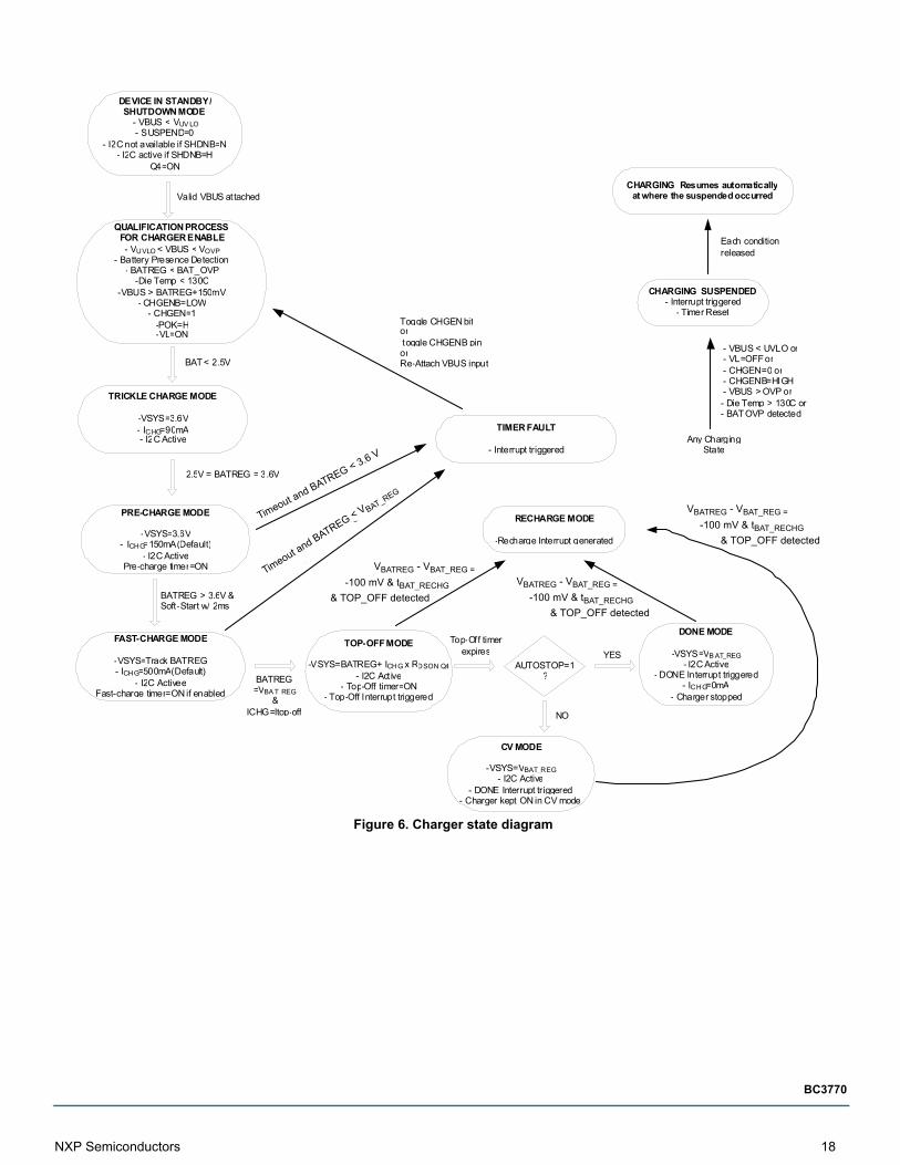
Figure 6. Charger state diagram
DEVICE IN STANDBY/SHUTDOWN MODE
- VBUS < VUV LO- SUSPEND= 0
- I2C not available if SHDNB=N- I2C active if SHDNB=H
Q4=ON
Valid VBUS attached
QUALIFICATION PROCESS FOR CHARGER ENABLE- VUVLO < VBUS < VOVP
- Battery Presence Detection- BATREG < BAT_OVP
-Die Temp < 130C-VBUS > BATREG+150mV
- CHGENB =LOW- CHGEN=1
-POK=H-VL=ON
TIMER FAULT
- Interrupt triggeredAny Charging
State
- VBUS < UVLO or- VL=OFF or- CHGEN=0 or- CHGENB=HIGH
TRICKLE CHARGE MODE
-VSYS=3.6V- ICHG=90mA- I2C Active
BAT < 2.5V
2.5V = BATREG = 3.6V
PRE-CHARGE MODE
-VSYS=3.6V- ICHG=150 mA (Default)
- I2C ActivePre-charge timer=ON
Timer-O
ut &
BATREG <3.6
V
FAST-CHARGE MODE
-VSYS=Track BATREG- ICHG=500mA(Default)
- I2C ActiveeFast-charge timer=ON if enabled
BATREG > 3.6V & Soft-Start w/ 2ms
TOP-OFF MODE
-VSYS=BATREG+ ICHG x RDSON_Q4
- I2C Act ive- Top-Off timer=ON
- Top-Off Interrupt triggered
BATREG =VBA T_REG
&ICHG=Itop -off
Timer-
Out &
BATR
EG <
VBAT_REG
DONE MODE
-VSYS=VB AT_REG- I2C Active
- DONE Interrupt triggered- ICHG=0mA
- Charger stopped
Top-Off timer expires
RECHARGE MODE
-Recharge Interrupt generated
AUTOSTOP=1?
YES
CV MODE
-VSYS=VBAT_REG- I2C Active
- DONE Interrupt triggered- Charger kept ON in CV mode
NO
VBATREG-VBAT_R
EG?
-100mV
& tBAT_RECHG
& Top-OFF detected
V BATREG-VBAT_REG ?
-100mV & tBAT_RECHG
& Top-OFF
detected
VBATREG-VBAT_REG ?
-100mV& tBAT_RECHG &
Top-Off detected
Toggle CHGEN bit ortoggle CHGENB pinor Re-Attach VBUS input
CHARGING SUSPENDED- Interrupt triggered
- Timer Reset
CHARGING Resumes automaticallyat where the suspended occurred
- VBUS > OVP or- Die Temp > 130C or- BAT OVP detected
Each condition released
Timeout and BATREG < 3.6 V
Timeout a
nd BATREG < V BAT_REG
VBATREG - VBAT_REG =
-100 mV & tBAT_RECHG
& TOP_OFF detected
VBATREG - VBAT_REG =
-100 mV & tBAT_RECHG
& TOP_OFF detected
VBATREG - VBAT_REG =
-100 mV & tBAT_RECHG
& TOP_OFF detected
19 NXP Semiconductors
BC3770
5.3.9 Safety timerThere are three safety timers on the device: a pre-charge timer, a fast charge timer, and a top-off timer. The pre-charge is fixed at 45 minutes, and the fast charge and the top-off timer are programmable over I2C. The reset conditions for each timer are described with the following.
1. Pre-charge timer is reset in one or more of the following ways:• BATREG crosses over the VSYS minimum threshold of 3.6 V• Falling VBUS UVLO detected• CHGENB = HIGH
2. Fast-charge timer is reset in one or more of the following ways:• BATREG hits the regulation voltage VBAT_REG and the charge current hits the top-off current threshold• Falling VBUS UVLO detected• CHGENB=HIGH or CHGEN reset to “0” before expiration
3. Top-off timer is reset in one or more of the following ways:• BATREG hits the regulation voltage VBAT_REG, the charge current hits the top-off current threshold, and the timer expires in
AUTOSTOP = 1• Falling VBUS UVLO detected• CHGENB = HIGH or CHGEN reset to “0” before expiration
However, all safety timers are reset commonly in the following fault conditions:
• BAT OVP detected• VBUS OVP detected• Thermal shutdown
If all fault conditions are released, the timer resumes to start.
5.3.10 VSYSWhen being charged from VBUS, if the battery voltage becomes close to the minimum system voltage threshold, VVSYS_MIN (3.6 V), VSYS tracks the battery voltage up to a preset VBAT_REG. A load current from an input is provided to both VSYS and the battery with up to a maximum input limit programmed value.
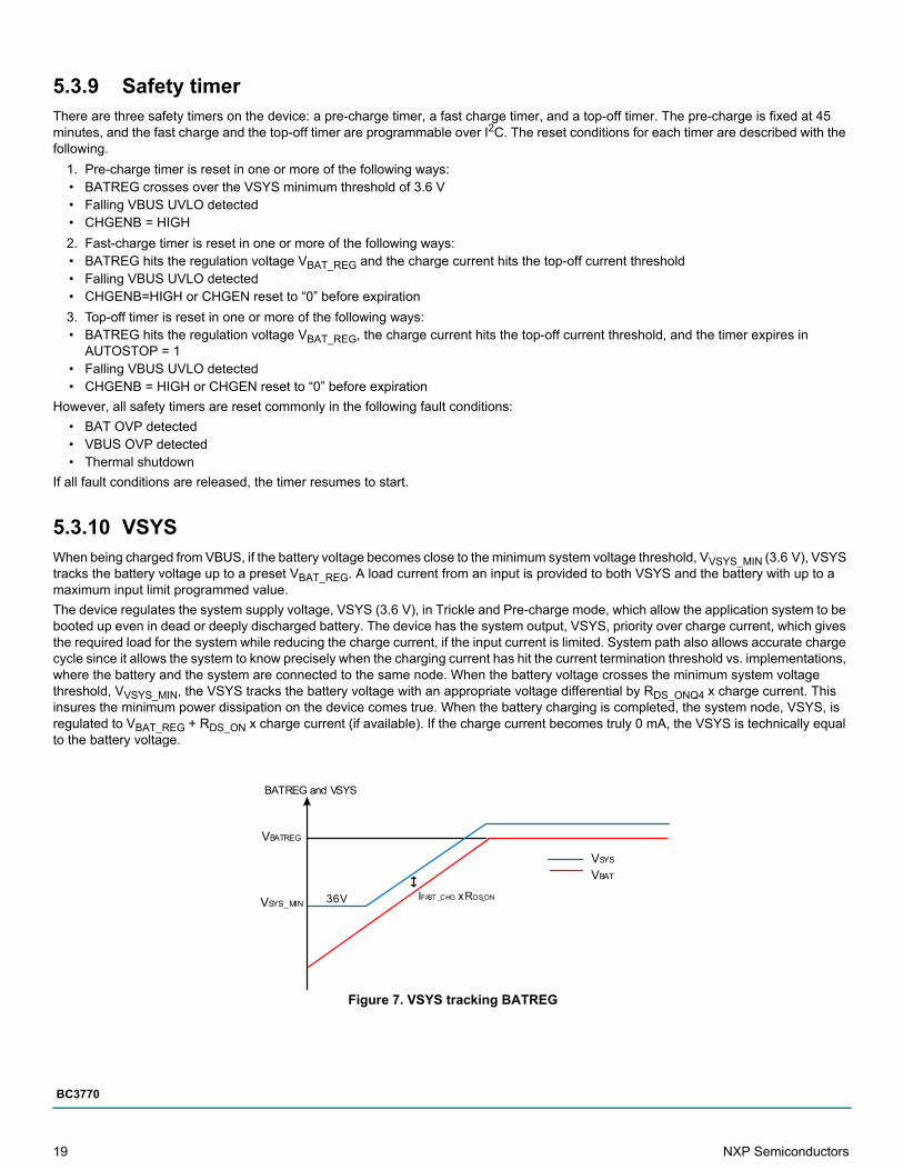
The device regulates the system supply voltage, VSYS (3.6 V), in Trickle and Pre-charge mode, which allow the application system to be booted up even in dead or deeply discharged battery. The device has the system output, VSYS, priority over charge current, which gives the required load for the system while reducing the charge current, if the input current is limited. System path also allows accurate charge cycle since it allows the system to know precisely when the charging current has hit the current termination threshold vs. implementations, where the battery and the system are connected to the same node. When the battery voltage crosses the minimum system voltage threshold, VVSYS_MIN, the VSYS tracks the battery voltage with an appropriate voltage differential by RDS_ONQ4 x charge current. This insures the minimum power dissipation on the device comes true. When the battery charging is completed, the system node, VSYS, is regulated to VBAT_REG + RDS_ON x charge current (if available). If the charge current becomes truly 0 mA, the VSYS is technically equal to the battery voltage.
Figure 7. VSYS tracking BATREG
BATREG and VSYS
VBATREG
VSYS_MIN 3.6V
VSYS
VBAT
IFAST _CHG x RDS_ON
NXP Semiconductors 20
BC3770
5.3.10.1 Charger enable control
The CHGEN bit in the control register and CHGENB pin are used to enable or disable the charging process.
Figure 8. Charger enable
If the CHGENB pin is not used in the application, leave the pin float since CHGENB has an internal 300 kΩ pull-down resistance to ground.
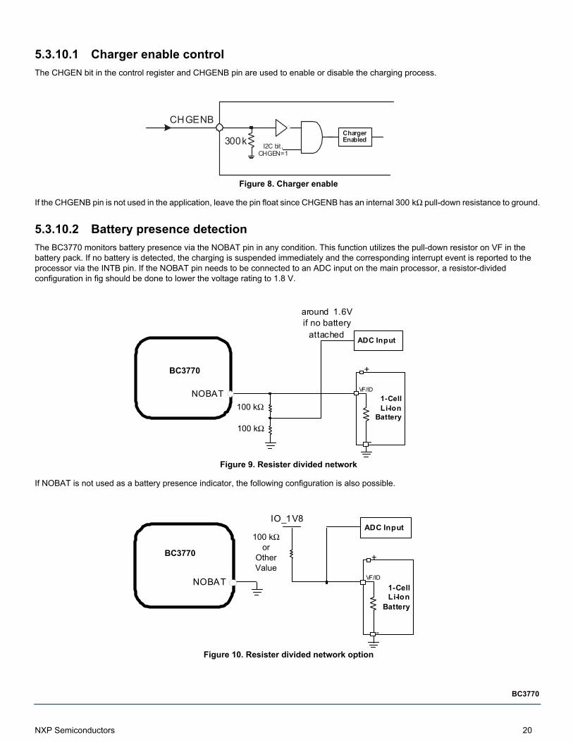
5.3.10.2 Battery presence detection
The BC3770 monitors battery presence via the NOBAT pin in any condition. This function utilizes the pull-down resistor on VF in the battery pack. If no battery is detected, the charging is suspended immediately and the corresponding interrupt event is reported to the processor via the INTB pin. If the NOBAT pin needs to be connected to an ADC input on the main processor, a resistor-divided configuration in fig should be done to lower the voltage rating to 1.8 V.
Figure 9. Resister divided network
If NOBAT is not used as a battery presence indicator, the following configuration is also possible.
Figure 10. Resister divided network option
CHGENB
300kChargerEnabled
I2C bit , CHGEN=1
1-CellLi-Ion
Battery
+
VF/ID
-
NOBAT
ADC Input
SM5418
100k?
100k?
around 1.6V if no battery
attached
BC3770
100 kΩ
100 kΩ
1-CellLi-Ion
Battery
+
VF/ID
-
NOBAT
ADC Input100k?
or other value
SM5418
IO_1V8
BC3770
100 kΩor
OtherValue
21 NXP Semiconductors
BC3770
5.3.10.3 Battery remote sensing
In order for the device to exactly regulate the + terminal on the battery cell as close to a preset VBAT_REG as possible, the BATREG and BATSNSN pins are used. In the real application, there may be some voltage drop between the CHGOUT pin and the + terminal, which comes from parasitic resistance, due to the PCB trace and a charge current. This voltage drop makes the VBAT_REG not regulate at the target regulation voltage. To reduce the charging time, place those two pins, BATREG and BATSNSN, as close to each + and - terminal on the battery pack as possible.
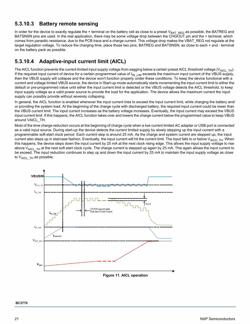
5.3.10.4 Adaptive-input current limit (AICL)
The AICL function prevents the current limited input supply voltage from sagging below a certain preset AICL threshold voltage (VAICL_TH). If the required input current of device for a certain programmed value of IIN_LIM exceeds the maximum input current of the VBUS supply, then the VBUS supply will collapse and the device won't function properly under these conditions. To keep the device functional with a current and voltage limited VBUS source, the device in Start-up mode automatically starts incrementing the input current limit to either the default or pre-programmed value until either the input current limit is detected or the VBUS voltage detects the AICL threshold, to keep input supply voltage as a valid power source to provide the load for the application. The device allows the maximum current the input supply can possibly provide without severely collapsing.
In general, the AICL function is enabled whenever the input current tries to exceed the input current limit, while charging the battery and/or providing the system load. At the beginning of the charge cycle with discharged battery, the required input current could be lower than the VBUS current limit. The input current increases as the battery voltage increases. Eventually, the input current may exceed the VBUS input current limit. If this happens, the AICL function takes over and lowers the charge current below the programmed value to keep VBUS around VAICL_TH.
Most of the time charge reduction occurs at the beginning of charge cycle when a low current limited AC adapter or USB port is connected as a valid input source. During start-up the device detects the current limited supply by slowly stepping up the input current with a programmable soft-start clock period. Each current step is around 25 mA. As the charge and system current are stepped up, the input current also steps up in staircase fashion. Eventually, the input current will hit the current limit. The input falls to or below VAICH_TH. When this happens, the device steps down the input current by 25 mA at the next clock rising edge. This allows the input supply voltage to rise above VAICL_TH at the next soft start clock cycle. The charge current is stepped up again by 25 mA. This again allows the input current to be exceed. The input reduction continues to step up and down the input current by 25 mA to maintain the input supply voltage as close to VAICL_TH as possible.
Figure 11. AICL operation
VAICL_TH
IIN_ LIM
IIN_ LIM
ICHG+SYS
VBAT
VBAT _RE G
IIN_LIM
VBUSIN
OTP-Programmable Soft Star t Clock Period
25mA
NXP Semiconductors 22
BC3770
5.3.10.5 Supplement mode
When the VSYS voltage falls below the battery voltage while a valid input is attached, the Q4 FET turns On and the Q4 FET gate regulates the gate drive of Q4 so the minimum VSYS stays at 50 mV below BATREG in the Supplement mode. This prevents oscillation from entering and exiting Supplement mode. As the discharge current increases, the Q4 gate is regulated with a higher voltage, to reduce RDS(on) until Q4 is full conduction.
5.3.10.6 Charging current reduction in VSYS overload
When the input current limit is detected in Charge mode by either a system overload or a programmed value is lower than the sum of load current and charge current, the device reduces the charge current until the limited input current falls below the preset current limit threshold, and the input voltage rises above the input voltage limit while maintaining the VSYS voltage at 3.4 V.
Although the charge current is reduced to 0 mA, the input power source is still overloaded, and the system voltage starts to drop. Once the system voltage falls 50 mV below the battery voltage, the device automatically enters the Supplement mode and the battery starts discharging so the system is supported from the both the input supply and battery. An corresponding interrupt for VSYS overload triggers via the INTB pin.
5.4 Protection and diagnosis features
5.4.1 Input overvoltage protectionWhen the input voltage exceeds the overvoltage protection (OVP) threshold, internal switches immediately turn off and disconnect the load and the charger from the power source, preventing damage to any downstream components. Simultaneously, the fault flag is triggered, alerting the system. As soon as the OVP event stays over the deglitch time, tINPUT_OVP, the converter resumes.
5.4.2 Battery (BAT) overvoltage protectionWhen the BATREG voltage exceeds the battery overvoltage protection threshold, VBAT_OVP (typ. VBAT_REG+ 0.1 V), the device turns off the PWM converter and sets the fault status bit. Simultaneously, the fault flag is asserted, alerting the system. There is a 0.1 V hysteresis in the internal threshold voltage. If the OVP event over the deglitch time is released, the converter and charging resume.
5.4.3 Reverse blockingIn the reverse blocking mode (VBUS - VBATREG) ≤ 50 mV (typ.), charging is disabled and the device is entered into Charger-suspended mode to minimize current drain from BATREG.
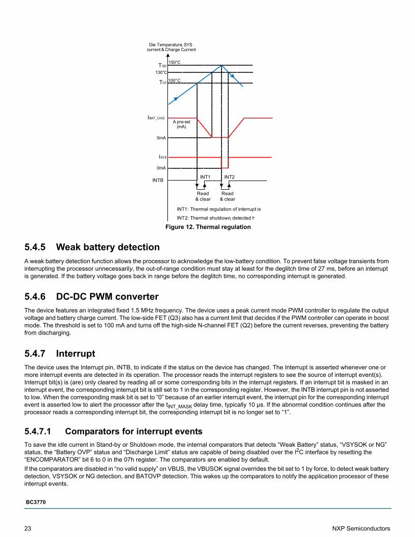
5.4.4 Thermal regulation and protectionWhen the device’s die temperature reaches TCF (around 100 °C), the device reduces the charge current by around 3.33% of the fast-charge current per °C. This drives the charge current down to 0 mA at 130 °C. Since the system load has priority over the battery charging, the battery charge current is reduced to 0 mA before the input limiter drops the system load current. If the junction temperature rises beyond 130 °C and then hits 150 °C, the PWM switcher shuts down to allow no input current from the input source. This prevents further die heating. In this condition, the system output voltage is regulated at BATREG. This internal thermal protection helps to improve device reliability. The device automatically goes back to normal operation when the die temperature cools down below 130 °C. In these thermal regulation and shutdown modes, I2C access is still active.
23 NXP Semiconductors
BC3770
Figure 12. Thermal regulation
5.4.5 Weak battery detectionA weak battery detection function allows the processor to acknowledge the low-battery condition. To prevent false voltage transients from interrupting the processor unnecessarily, the out-of-range condition must stay at least for the deglitch time of 27 ms, before an interrupt is generated. If the battery voltage goes back in range before the deglitch time, no corresponding interrupt is generated.
5.4.6 DC-DC PWM converterThe device features an integrated fixed 1.5 MHz frequency. The device uses a peak current mode PWM controller to regulate the output voltage and battery charge current. The low-side FET (Q3) also has a current limit that decides if the PWM controller can operate in boost mode. The threshold is set to 100 mA and turns off the high-side N-channel FET (Q2) before the current reverses, preventing the battery from discharging.
5.4.7 InterruptThe device uses the Interrupt pin, INTB, to indicate if the status on the device has changed. The Interrupt is asserted whenever one or more interrupt events are detected in its operation. The processor reads the interrupt registers to see the source of interrupt event(s). Interrupt bit(s) is (are) only cleared by reading all or some corresponding bits in the interrupt registers. If an interrupt bit is masked in an interrupt event, the corresponding interrupt bit is still set to 1 in the corresponding register. However, the INTB interrupt pin is not asserted to low. When the corresponding mask bit is set to “0” because of an earlier interrupt event, the interrupt pin for the corresponding interrupt event is asserted low to alert the processor after the tINT_MASK delay time, typically 10 µs. If the abnormal condition continues after the processor reads a corresponding interrupt bit, the corresponding interrupt bit is no longer set to “1”.
5.4.7.1 Comparators for interrupt events
To save the idle current in Stand-by or Shutdown mode, the internal comparators that detects “Weak Battery” status, “VSYSOK or NG” status, the “Battery OVP” status and “Discharge Limit” status are capable of being disabled over the I2C interface by resetting the “ENCOMPARATOR” bit 6 to 0 in the 07h register. The comparators are enabled by default.
If the comparators are disabled in “no valid supply” on VBUS, the VBUSOK signal overrides the bit set to 1 by force, to detect weak battery detection, VSYSOK or NG detection, and BATOVP detection. This wakes up the comparators to notify the application processor of these interrupt events.
IBAT_CHG
Die Temperature, SYS current & Charge Current
INTB
Read & clear
TCF 100°C
TSD150°C
0mA
A pre-set (mA)
130°C
ISYS
0mA
Read & clear
INT1: Thermal regulation of interrupt is asserted.
INT1 INT2
INT2: Thermal shutdown, detected by TDIE=150°C.
NXP Semiconductors 24
BC3770
5.5 Logic commands and registers
5.5.1 Serial interfaceI2C is a two-wire serial interface developed by Phillips Semiconductor. The bus consists of a data line, SDA, and a clock line, SCL, with pull-up structures. When the bus is idle, both the SDA and SCL lines are pulled high. All the I2C compatible devices connect to the I2C bus through open drain I/O pins, SDA, and SCL. A master generates the clock signal and device addresses. The master also generates specific conditions that indicate the START and STOP of data transfer. A slave device receives and/or transmits data on the bus under the master device.
The device works as a slave and is compatible with the following data transfer modes, as defined in the I2C-Bus Specification: Standard mode (100 kbps) and Fast mode (400 kbps). The interface adds flexibility to all necessary control options of the program, and enables most functions to be programmed to the new values, depending on the instantaneous application requirements. I2C is asynchronous, which means that it runs off of SCL.The data transfer protocol for Standard and Fast modes is exactly the same.
5.5.1.1 Bus speed
The device I2C interface supports bus SCL clock speeds up to 400 kbps for Full-speed mode. The SCL and SDA input buffers incorporate spike suppression and Schmitt triggers to reject short glitches, as required by the I2C specifications.
5.5.1.2 Data validity
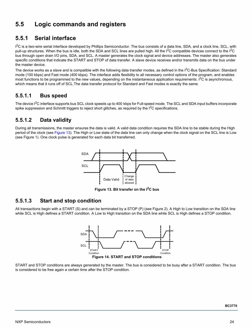
During all transmissions, the master ensures the data is valid. A valid data condition requires the SDA line to be stable during the High period of the clock (see Figure 13). The High or Low state of the data line can only change when the clock signal on the SCL line is Low (see Figure 1). One clock pulse is generated for each data bit transferred.
Figure 13. Bit transfer on the I2C bus
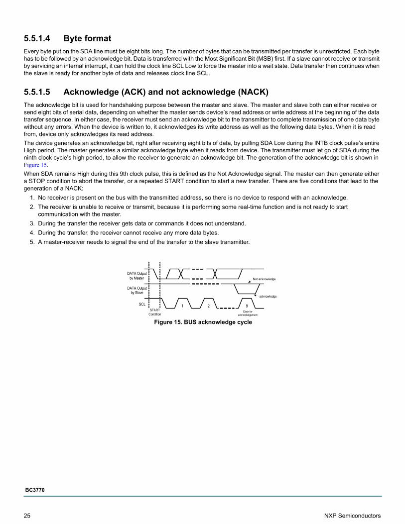
5.5.1.3 Start and stop condition
All transactions begin with a START (S) and can be terminated by a STOP (P) (see Figure 2). A High to Low transition on the SDA line while SCL is High defines a START condition. A Low to High transition on the SDA line while SCL is High defines a STOP condition.
Figure 14. START and STOP conditions
START and STOP conditions are always generated by the master. The bus is considered to be busy after a START condition. The bus is considered to be free again a certain time after the STOP condition.
SDA
SCL
Data ValidChange of data allowed
SDA
SCL
START Condition
STOPCondition
25 NXP Semiconductors
BC3770
5.5.1.4 Byte format
Every byte put on the SDA line must be eight bits long. The number of bytes that can be transmitted per transfer is unrestricted. Each byte has to be followed by an acknowledge bit. Data is transferred with the Most Significant Bit (MSB) first. If a slave cannot receive or transmit by servicing an internal interrupt, it can hold the clock line SCL Low to force the master into a wait state. Data transfer then continues when the slave is ready for another byte of data and releases clock line SCL.
5.5.1.5 Acknowledge (ACK) and not acknowledge (NACK)
The acknowledge bit is used for handshaking purpose between the master and slave. The master and slave both can either receive or send eight bits of serial data, depending on whether the master sends device’s read address or write address at the beginning of the data transfer sequence. In either case, the receiver must send an acknowledge bit to the transmitter to complete transmission of one data byte without any errors. When the device is written to, it acknowledges its write address as well as the following data bytes. When it is read from, device only acknowledges its read address.
The device generates an acknowledge bit, right after receiving eight bits of data, by pulling SDA Low during the INTB clock pulse’s entire High period. The master generates a similar acknowledge byte when it reads from device. The transmitter must let go of SDA during the ninth clock cycle’s high period, to allow the receiver to generate an acknowledge bit. The generation of the acknowledge bit is shown in Figure 15.
When SDA remains High during this 9th clock pulse, this is defined as the Not Acknowledge signal. The master can then generate either a STOP condition to abort the transfer, or a repeated START condition to start a new transfer. There are five conditions that lead to the generation of a NACK:
1. No receiver is present on the bus with the transmitted address, so there is no device to respond with an acknowledge.
2. The receiver is unable to receive or transmit, because it is performing some real-time function and is not ready to start communication with the master.
3. During the transfer the receiver gets data or commands it does not understand.
4. During the transfer, the receiver cannot receive any more data bytes.
5. A master-receiver needs to signal the end of the transfer to the slave transmitter.
Figure 15. BUS acknowledge cycle
Not acknowledge
acknowledge
DATA Output by Master
START Condition
Clock for acknowledgement
SCL
DATA Output by Slave
1 2 9
NXP Semiconductors 26
BC3770
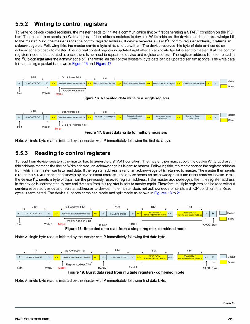
5.5.2 Writing to control registersTo write to device control registers, the master needs to initiate a communication link by first generating a START condition on the I2C bus. The master then sends the Write address. If the address matches to device’s Write address, the device sends an acknowledge bit to the master. Next, the master sends the control register address. If device receives a valid I2C control register address, it returns an acknowledge bit. Following this, the master sends a byte of data to be written. The device receives this byte of data and sends an acknowledge bit back to master. The internal control register is updated right after an acknowledge bit is sent to master. If all the control registers need to be updated at once, there is no need to repeat the device and register address. The register address is incremented in the I2C block right after the acknowledge bit. Therefore, all the control registers’ byte data can be updated serially at once. The write data format in single packet is shown in Figure 16 and Figure 17.
Figure 16. Repeated data write to a single register
Figure 17. Burst data write to multiple registers
Note: A single byte read is initiated by the master with P immediately following the first data byte.
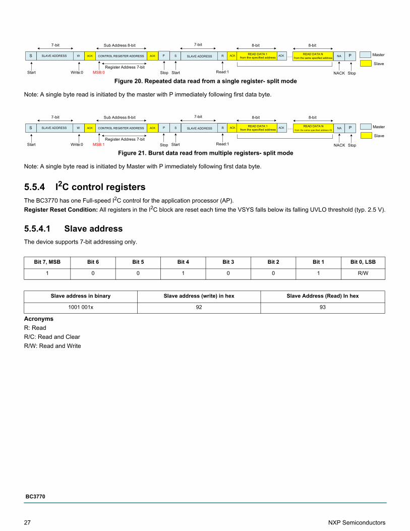
5.5.3 Reading to control registersTo read from device registers, the master has to generate a START condition. The master then must supply the device Write address. If this address matches the device Write address, an acknowledge bit is sent to master. Following this, the master sends the register address from which the master wants to read data. If the register address is valid, an acknowledge bit is returned to master. The master then sends a repeated START condition followed by device Read address. The device sends an acknowledge bit if the Read address is valid. Next, the device I2C sends a byte of data from the previously received register address. If the master acknowledges, then the register address in the device is incremented by one and the data from this register is sent to master again. Therefore, multiple registers can be read without sending repeated device and register addresses to device. If the master does not acknowledge or sends a STOP condition, the Read cycle is terminated. The device supports combined mode and split mode as shown in Figures 18 to 21.
Figure 18. Repeated data read from a single register- combined mode
Note: A single byte read is initiated by the master with P immediately following first data byte.
Figure 19. Burst data read from multiple registers- combined mode
Note: A single byte read is initiated by the master with P immediately following first data byte.
Master
SlaveS ACKSLAVE ADDRESS W ACK Data to the Control Register P
7-bit
Start Write:0
8-bit
MSB:0
Data to the Control RegisterCONTROL REGISTER ADDRESS ACK ACK ACK ACK
Sub Address 8-bit
Register Address 7-bit
Data to the Control Register Data to the Control Register
Master
SlaveS ACKSLAVE ADDRESS W ACK P
7-bit
Start Write:0
8-bit
MSB:1
Data to the Control Register K+1CONTROL REGISTER ADDRESS ACK ACK ACK ACK
Sub Address 8-bit
K Register Address 7-bit
Data to the Control Register K
Data to the Control Register K+2
Data to the Control Register K+N-1
S ACKSLAVE ADDRESS W ACKREAD DATA 1
from the specified address NASrCONTROL REGISTER ADDRESS RR PACK
7-bit
Start Write:0
Sub Address 8-bit
Re-Start
SLAVE ADDRESS
Read:1
7-bit
…. READ DATA Nfrom the same specified address
Master
Slave
8-bit
NACK
ACK
StopMSB:0 Register Address 7-bit
8-bit
S ACKSLAVE ADDRESS W ACKREAD DATA 1
from the specified address NASrCONTROL REGISTER ADDRESS RR PACK
7-bit
Start Write:0
Sub Address 8-bit
Re-Start
SLAVE ADDRESS
Read:1
7-bit
…. READ DATA Nfrom the same specified address +N
Master
Slave
8-bit
NACK
ACK
StopMSB:1 Register Address 7-bit
8-bit
27 NXP Semiconductors
BC3770
Figure 20. Repeated data read from a single register- split mode
Note: A single byte read is initiated by the master with P immediately following first data byte.
Figure 21. Burst data read from multiple registers- split mode
Note: A single byte read is initiated by Master with P immediately following first data byte.
5.5.4 I2C control registersThe BC3770 has one Full-speed I2C control for the application processor (AP).
Register Reset Condition: All registers in the I2C block are reset each time the VSYS falls below its falling UVLO threshold (typ. 2.5 V).
5.5.4.1 Slave address
The device supports 7-bit addressing only.
Acronyms
R: Read
R/C: Read and Clear
R/W: Read and Write
Bit 7, MSB Bit 6 Bit 5 Bit 4 Bit 3 Bit 2 Bit 1 Bit 0, LSB
1 0 0 1 0 0 1 R/W
Slave address in binary Slave address (write) in hex Slave Address (Read) In hex
1001 001x 92 93
S ACKSLAVE ADDRESS W ACKREAD DATA 1
from the specified address NASCONTROL REGISTER ADDRESS RR PACK
7-bit
Start Write:0
Sub Address 8-bit
Stop
SLAVE ADDRESS
Read:1
7-bit
…. READ DATA Nfrom the same specified address
Master
Slave
8-bit
NACK
ACK
StopMSB:0 Register Address 7-bit
8-bit
P
Start
S ACKSLAVE ADDRESS W ACKREAD DATA 1
from the specified address NASCONTROL REGISTER ADDRESS RR PACK
7-bit
Start Write:0
Sub Address 8-bit
Stop
SLAVE ADDRESS
Read:1
7-bit
…. READ DATA Nfrom the same specified address +N
Master
Slave
8-bit
NACK
ACK
StopMSB:1 Register Address 7-bit
8-bit
P
Start
NXP Semiconductors 28
BC3770
5.5.5 Control register map
5.5.5.1 INT1: interrupt register 1 for abnormal conditions
Address(hex)
Register name
Reset(hex)
Bit 7 Bit 6 Bit 5 Bit 4 Bit 3 Bit 2 Bit 1 Bit 0
00 INT1 00 VBUSOVP VBUSUVLO VBUSINOK AICL VBUSLIMIT BATOVP THEMSHDN THEMREG
01 INT2 00 FASTTMROFF NOBAT WEAKBAT OTGFAIL PRETMROFF CHGRSTF DONE TOPOFF
02 INT3 00 Reserved Reserved Reserved Reserved VSYSOK VSYSNG VSYSOLP DISLIMIT
03 INTMSK1 03 VBUSOVPM VBUSUVLOM VBUSINOKM AICLMVBUSINLIMIT
MBATOVPM THEMSHDNM THEMREGM
04 INTMSK2 B8FASTTMROFF
MNOBATM WEAKBATM OTGFAILM
PRETMROFFM
CHGRSTFM DONEM TOPOFFM
05 INTMSK3 FF Reserved Reserved Reserved Reserved VSYSOKM VSYSNGM VSYSOLPM DISLIMITM
06 STATUS N/A Reserved Reserved Reserved VSYSOLP DISLIMIT THEMSHDN BATDET SUSPEND
07 CTRL 42 ReservedENCOMPARA
TORReserved Reserved RESET SUSPEN CHGEN ENBOOST
08 VBUSCTRL 08 Reserved Reserved VBUSLIMIT
09 CHGCTRL1 2F Reserved AICLTH AUTOSTOP AICLEN PRECHG
0A CHGCTRL2 08 Reserved Reserved FASTCHG
0B CHGCTRL3 4C BATREG WEAKBAT
0C CHGCTRL4 05 Reserved TOPOFF DISLIMIT
0D CHGCTRL5 0F Reserved Reserved VOTG FASTTIMER TOPOFFTIMER
Address (hex) Mode Reset condition:VSYS ≤ VSYS_UVLO
Reset: 0x0000 R/C
Bit Name Reset Description
7 VBUSOVP 0 1: VBUS OVP event detected
6 VBUSUVLO 0 1: VBUS falling UVLO detected
5 VBUSINOK 0 1: Valid VBUS detected
4 AICL 0 1: AICL threshold detected
3 VBUSLIMIT 0 1: VBUS input current limit detected
2 BATOVP (17), (18) 0 1: BAT OVP detected
1 THEMSHDN 0 1: Thermal shutdown detected
0 THEMREG 0 1: Thermal regulation threshold detected
Notes17. These interrupts are to be set to 1 when “ENCOMPARATOR” bit 7 in the 07h register set to “1” AND no valid VBUS supply is at preset. If
“ENCOMPARATOR” bit 7 is reset to “0” in no valid VBUS supply, these interrupt events are in no response.18. These interrupts are to be forcibly overridden to alert the interrupt events in a valid VBUS attached.
29 NXP Semiconductors
BC3770
5.5.5.2 INT2: interrupt register 2
5.5.5.3 INT3: interrupt register 3
Address (hex) Mode Reset condition:VSYS ≤ VSYS_UVLO
Reset: 0x0001 R/C
Bit Name Reset Description
7 FASTTMROFF 0 1: Fast charger timer expired
6 NOBAT 0 1: No battery threshold detected
5 WEAKBAT (19), (20) 0 1: Weak battery threshold detected
4 OTGFAIL 0 1: Boost failed detected due to overload
3 PRETMROFF 0 1: Pre-charge timer expired
2 CHGRSTF 0 1: Charger restart detected
1 DONE 0 1: Top-off charge timer expired
0 TOPOFF 0 1: Top-off threshold is detected
Notes19. These interrupts are to be set to 1 when “ENCOMPARATOR” bit 7 in the 07h register set to “1” AND no valid VBUS supply is at preset. If
“ENCOMPARATOR” bit 7 is reset to “0” in no valid VBUS supply, these interrupt events are in no response.20. These interrupts are to be forcibly overridden to alert the interrupt events in a valid VBUS attached.
Address (hex) Mode Reset condition:VSYS ≤ VSYS_UVLO
Reset: 0x0002 R/C
Bit Name Reset Description
7:4 Reserved 0000 Write “0000”
3 VSYSOK (21), (22) 0 1: VSYS rising 3.6 V detected in a valid VBUS attached
2 VSYSNG (21), (22) 0 1: VSYS falling 3.4 V detected in a valid VBUS attached
1 VSYSOLP 01: VSYS overload condition debounced is detected (VSYS ≤ 3.4 V) in a valid VBUS attached
0 DISLIMIT (21) 0 1: Current limit threshold detected in discharge mode
Notes21. These interrupts are to be set to 1 when “ENCOMPARATOR” bit 7 in the 07h register set to “1” AND no valid VBUS supply is at preset. If
“ENCOMPARATOR” bit 7 is reset to “0” in no valid VBUS supply, these interrupt events are in no response.22. These interrupts are to be forcibly overridden to alert the interrupt events in a valid VBUS attached.
NXP Semiconductors 30
BC3770
5.5.5.4 INTMSK1: interrupt mask register 1
5.5.5.5 INTMSK2: interrupt mask register 2
Address (hex) MODE Reset condition:VSYS ≤ VSYS_UVLO
Reset: 0x0303 R/W
Bit Name Reset Description
7 VBUSOVPM 00: Interrupt is enabled1: VBUS OVP interrupt masked
6 VBUSUVLOM 00: Interrupt is enabled1: VBUS falling UVLO interrupt masked
5 VBUSINOKM 00: Interrupt is enabled1: Valid VBUS interrupt masked
4 AICLM 00: Interrupt is enabled1: AICL interrupt masked
3 VBUSINLIMITM 00: Interrupt is enabled1: VBUS Input Current Limit interrupt masked
2 BATOVPM 00: Interrupt is enabled1: BAT OVP interrupt masked
1 THEMSHDNM 10: Interrupt is enabled1: Thermal shutdown interrupt masked
0 THEMREGM 10: Interrupt is enabled1: Thermal regulation interrupt masked
Address (hex) Mode Reset condition:VSYS ≤ VSYS_UVLO
Reset: 0xB804 R/W
Bit Name Reset Description
7 FASTTMROFFM 10: Interrupt is enabled1: Fast charger timer expired interrupt masked
6 NOBATM 00: Interrupt is enabled1: No Battery interrupt masked
5 WEAKBATM 10: Interrupt is enabled1: Weak battery interrupt masked
4 OTGFAILM 10: Interrupt is enabled1: Boost failed interrupt masked
3 PRETMROFFM 10: Interrupt is enabled1: Pre-charge timer expired interrupt masked
2 CHGRSTFM 00: Interrupt is enabled1: Charger restart interrupt masked
1 DONEM 00: Interrupt is enabled1: Done interrupt masked
0 TOPOFFM 00: Interrupt is enabled1: Top-Off threshold interrupt masked

31 NXP Semiconductors
BC3770
5.5.5.6 INTMSK3: interrupt mask register 3
5.5.5.7 STATUS – status register
Address (hex) Mode Reset condition:VSYS ≤ VSYS_UVLO
Reset: 0xFF05 R/W
Bit Name Reset Description
7:4 Reserved 1111 Write “1111”
3 VSYSOKM 10: Interrupt is enabled1: VSYS rising 3.6 V detection masked
2 VSYSNGM 10: Interrupt is enabled1: VSYS falling 3.4 V detection masked
1 VSYSOLPM 10: Interrupt is enabled1: VSYS overload condition detection masked
0 DISLIMITM 10: Interrupt is enabled1: Current limit threshold detection masked
Address(hex)
Mode Reset condition:VSYS ≤ VSYS_UVLO
Reset: N/A
06 R
Bit Name Reset Description
7:5 Reserved Reserved for future use
4 VSYSOLP0: VSYS output is healthy (3.6 V ≤ VSYS ≤ VBAT_REG)1: VSYS overloaded with a valid VBUS (VSYS ≤ 3.4 V)
3 DISLIMIT0: Current limit threshold not detected in discharge mode1: Current limit threshold detected in discharge mode
2 THEMSHDN0: The die temperature is less than 130 °C.1: The die temperature is between 150 °C and 130 °C
1 BATDET0: Battery detached (No Battery)1: Battery attached (Battery at present)
0 SUSPEND0: Suspend mode is disabled1: Suspend mode is enabled
NXP Semiconductors 32
BC3770
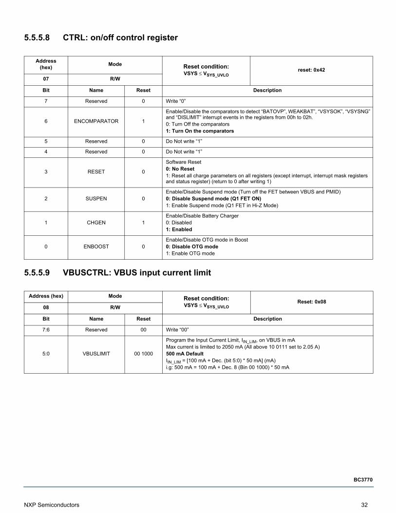
5.5.5.8 CTRL: on/off control register
5.5.5.9 VBUSCTRL: VBUS input current limit
Address(hex)
Mode Reset condition:VSYS ≤ VSYS_UVLO
reset: 0x42
07 R/W
Bit Name Reset Description
7 Reserved 0 Write “0”
6 ENCOMPARATOR 1
Enable/Disable the comparators to detect “BATOVP”, WEAKBAT”, “VSYSOK”, “VSYSNG” and “DISLIMIT” interrupt events in the registers from 00h to 02h.0: Turn Off the comparators 1: Turn On the comparators
5 Reserved 0 Do Not write “1”
4 Reserved 0 Do Not write “1”
3 RESET 0
Software Reset0: No Reset1: Reset all charge parameters on all registers (except interrupt, interrupt mask registers and status register) (return to 0 after writing 1)
2 SUSPEN 0Enable/Disable Suspend mode (Turn off the FET between VBUS and PMID)0: Disable Suspend mode (Q1 FET ON)1: Enable Suspend mode (Q1 FET in Hi-Z Mode)
1 CHGEN 1Enable/Disable Battery Charger0: Disabled1: Enabled
0 ENBOOST 0Enable/Disable OTG mode in Boost0: Disable OTG mode1: Enable OTG mode
Address (hex) Mode Reset condition:VSYS ≤ VSYS_UVLO
Reset: 0x0808 R/W
Bit Name Reset Description
7:6 Reserved 00 Write “00”
5:0 VBUSLIMIT 00 1000
Program the Input Current Limit, IIN_LIM, on VBUS in mAMax current is limited to 2050 mA (All above 10 0111 set to 2.05 A)500 mA DefaultIIN_LIM = [100 mA + Dec. (bit 5:0) * 50 mA] (mA)i.g: 500 mA = 100 mA + Dec. 8 (Bin 00 1000) * 50 mA
33 NXP Semiconductors
BC3770
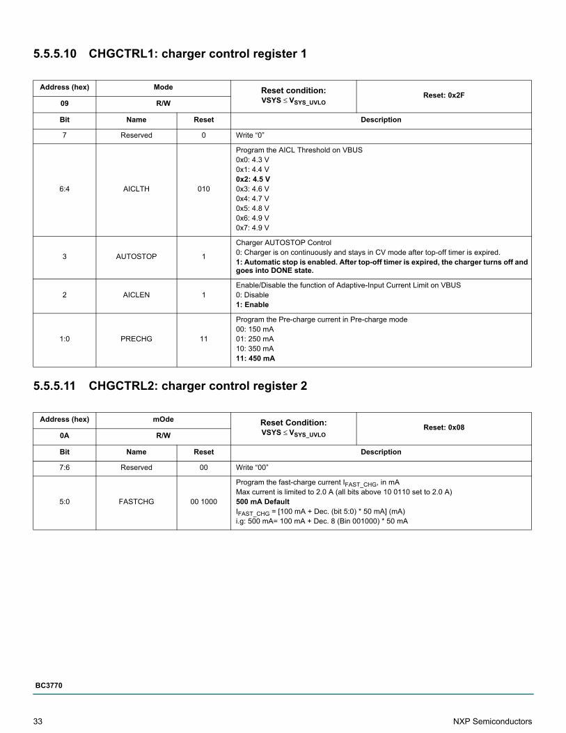
5.5.5.10 CHGCTRL1: charger control register 1
5.5.5.11 CHGCTRL2: charger control register 2
Address (hex) Mode Reset condition:VSYS ≤ VSYS_UVLO
Reset: 0x2F09 R/W
Bit Name Reset Description
7 Reserved 0 Write “0”
6:4 AICLTH 010
Program the AICL Threshold on VBUS0x0: 4.3 V0x1: 4.4 V0x2: 4.5 V0x3: 4.6 V0x4: 4.7 V0x5: 4.8 V0x6: 4.9 V0x7: 4.9 V
3 AUTOSTOP 1
Charger AUTOSTOP Control0: Charger is on continuously and stays in CV mode after top-off timer is expired.1: Automatic stop is enabled. After top-off timer is expired, the charger turns off and goes into DONE state.
2 AICLEN 1Enable/Disable the function of Adaptive-Input Current Limit on VBUS0: Disable 1: Enable
1:0 PRECHG 11
Program the Pre-charge current in Pre-charge mode00: 150 mA01: 250 mA10: 350 mA11: 450 mA
Address (hex) mOde Reset Condition:VSYS ≤ VSYS_UVLO
Reset: 0x080A R/W
Bit Name Reset Description
7:6 Reserved 00 Write “00”
5:0 FASTCHG 00 1000
Program the fast-charge current IFAST_CHG, in mAMax current is limited to 2.0 A (all bits above 10 0110 set to 2.0 A)500 mA DefaultIFAST_CHG = [100 mA + Dec. (bit 5:0) * 50 mA] (mA)i.g: 500 mA= 100 mA + Dec. 8 (Bin 001000) * 50 mA
NXP Semiconductors 34
BC3770
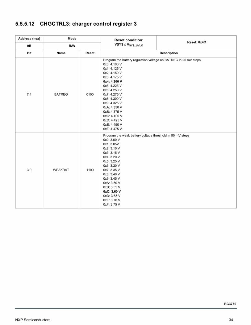
5.5.5.12 CHGCTRL3: charger control register 3
Address (hex) Mode Reset condition:VSYS ≤ VSYS_UVLO
Reset: 0x4C0B R/W
Bit Name Reset Description
7:4 BATREG 0100
Program the battery regulation voltage on BATREG in 25 mV steps0x0: 4.100 V0x1: 4.125 V0x2: 4.150 V0x3: 4.175 V0x4: 4.200 V0x5: 4.225 V0x6: 4.250 V0x7: 4.275 V0x8: 4.300 V0x9: 4.325 V0xA: 4.350 V0xB: 4.375 V0xC: 4.400 V0xD: 4.425 V0xE: 4.450 V0xF: 4.475 V
3:0 WEAKBAT 1100
Program the weak battery voltage threshold in 50 mV steps0x0: 3.00 V0x1: 3.05V0x2: 3.10 V0x3: 3.15 V0x4: 3.20 V0x5: 3.25 V0x6: 3.30 V0x7: 3.35 V0x8: 3.40 V0x9: 3.45 V0xA: 3.50 V0xB: 3.55 V0xC: 3.60 V0xD: 3.65 V0xE: 3.70 V0xF: 3.75 V
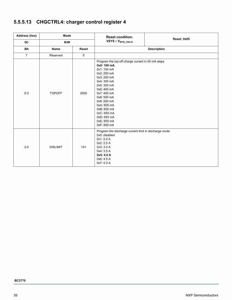
35 NXP Semiconductors
BC3770
5.5.5.13 CHGCTRL4: charger control register 4
Address (hex) Mode Reset condition:VSYS ≤ VSYS_UVLO
Reset: 0x050C R/W
Bit Name Reset Description
7 Reserved 0
6:3 TOPOFF 0000
Program the top-off charge current in 50 mA steps0x0: 100 mA0x1: 150 mA0x2: 200 mA0x3: 250 mA0x4: 300 mA0x5: 350 mA0x6: 400 mA0x7: 450 mA0x8: 500 mA0x9: 550 mA0xA: 600 mA0xB: 650 mA0xC: 650 mA0xD: 650 mA0xE: 650 mA0xF: 650 mA
2:0 DISLIMIT 101
Program the discharge current limit in discharge mode0x0: disabled0x1: 2.0 A0x2: 2.5 A0x3: 3.0 A0x4: 3.5 A0x5: 4.0 A0x6: 4.5 A0x7: 5.0 A
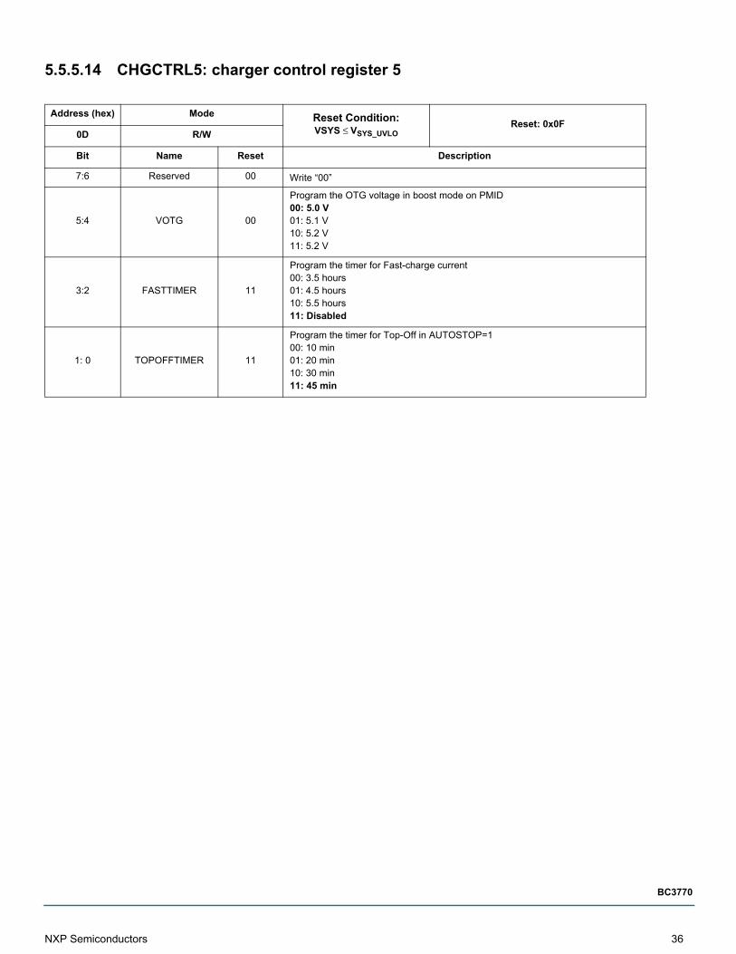
NXP Semiconductors 36
BC3770
5.5.5.14 CHGCTRL5: charger control register 5
Address (hex) Mode Reset Condition:VSYS ≤ VSYS_UVLO
Reset: 0x0F0D R/W
Bit Name Reset Description
7:6 Reserved 00 Write “00”
5:4 VOTG 00
Program the OTG voltage in boost mode on PMID00: 5.0 V 01: 5.1 V10: 5.2 V11: 5.2 V
3:2 FASTTIMER 11
Program the timer for Fast-charge current00: 3.5 hours 01: 4.5 hours10: 5.5 hours11: Disabled
1: 0 TOPOFFTIMER 11
Program the timer for Top-Off in AUTOSTOP=100: 10 min 01: 20 min10: 30 min11: 45 min
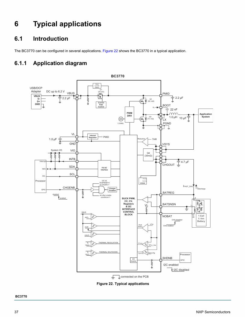
37 NXP Semiconductors
BC3770
6 Typical applications
6.1 Introduction
The BC3770 can be configured in several applications. Figure 22 shows the BC3770 in a typical application.
6.1.1 Application diagram
Figure 22. Typical applications
DC up to 6.2 V
Interrupt
SDA
SCL
Processor
GPIO
Processor
GPIO
1-CellLi-Ion
Battery
VBUS
LX
CurrentPath
Control
150 CTj
PGND
+
VF/ID
-
BUCK PWM,CC, CV,
Registers& I2C
INTERFACECONTROL
BLOCKAICL
OVP
UVLO
+
-
+
-
+
-
THERMAL SHUTDOWN
System I/O
GND
2.2 μF
ApplicationSystem
IFAST_CHG
PWMDRV
VBUS
VTH
Idischarge
+
-
VTrickle
VTH_TRK
WeakBattery
2.2 μFPMID
BOOT
+
-Vprechg Vpre-chg
InputCurrentDetect
Linear
ITrickle
Iprechg
VBUSD-D+
GND
USB/DCPAdapter
Q1(50 mΩ)
Q2(50 mΩ)
Q3(70 mΩ)
NOBAT
+
-
SDA
SCL
INTB
FS I2CInterface
VL
CHGENB
VSYS
BC3770
disabled
enabled
1.5 MHz
VL
All other enable conditions=1
ChargerEnabled
I2C bit,SUSPEND=0& CHGEN=1
1-CellLi-Ion
Battery
BATSNSN
VL InternalRegulator PMID
+
-
Q4(30mΩ)
THRReduction
100 CTj
+
-
THERMAL REGULATION
CHG disabled
CHG enabled
1.0 μF
22 nF
1.0 μH 10 μF
4.7 μF
SHDNB
CHGOUT
BATREG
I2Cdisable
I2C enabled
I2C disabled
connected on the PCB
VIO
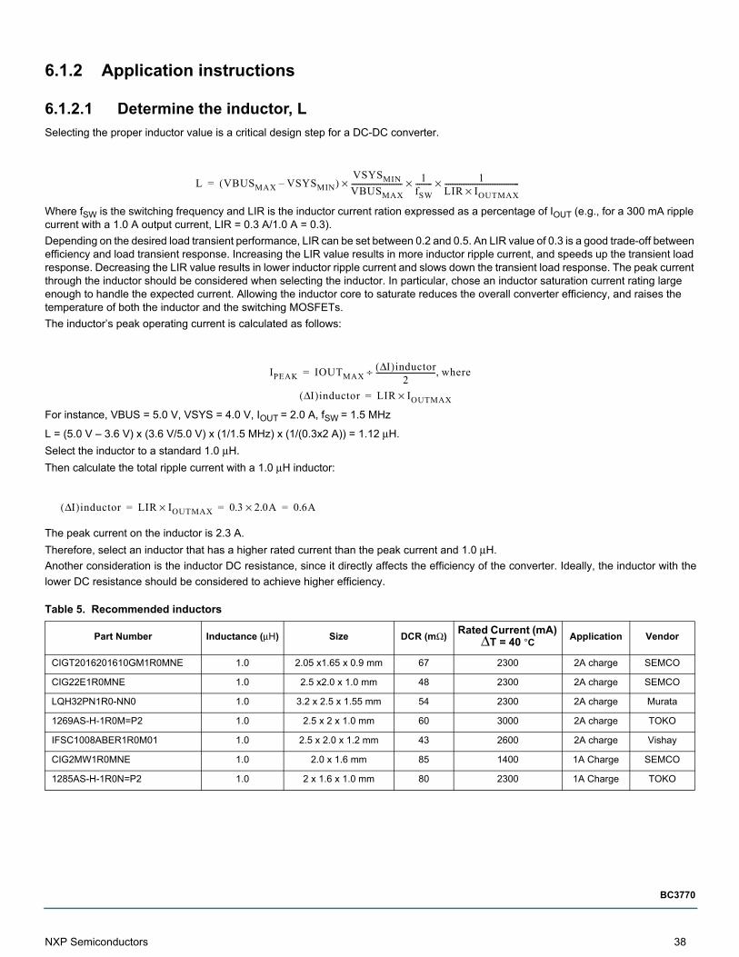
NXP Semiconductors 38
BC3770
6.1.2 Application instructions
6.1.2.1 Determine the inductor, L
Selecting the proper inductor value is a critical design step for a DC-DC converter.
Where fSW is the switching frequency and LIR is the inductor current ration expressed as a percentage of IOUT (e.g., for a 300 mA ripple current with a 1.0 A output current, LIR = 0.3 A/1.0 A = 0.3).
Depending on the desired load transient performance, LIR can be set between 0.2 and 0.5. An LIR value of 0.3 is a good trade-off between efficiency and load transient response. Increasing the LIR value results in more inductor ripple current, and speeds up the transient load response. Decreasing the LIR value results in lower inductor ripple current and slows down the transient load response. The peak current through the inductor should be considered when selecting the inductor. In particular, chose an inductor saturation current rating large enough to handle the expected current. Allowing the inductor core to saturate reduces the overall converter efficiency, and raises the temperature of both the inductor and the switching MOSFETs.
The inductor’s peak operating current is calculated as follows:
For instance, VBUS = 5.0 V, VSYS = 4.0 V, IOUT = 2.0 A, fSW = 1.5 MHz
L = (5.0 V – 3.6 V) x (3.6 V/5.0 V) x (1/1.5 MHz) x (1/(0.3x2 A)) = 1.12 μH.
Select the inductor to a standard 1.0 μH.
Then calculate the total ripple current with a 1.0 μH inductor:
The peak current on the inductor is 2.3 A.
Therefore, select an inductor that has a higher rated current than the peak current and 1.0 μH.
Another consideration is the inductor DC resistance, since it directly affects the efficiency of the converter. Ideally, the inductor with the
lower DC resistance should be considered to achieve higher efficiency.
Table 5. Recommended inductors
Part Number Inductance (μH) Size DCR (mΩ)Rated Current (mA)
ΔT = 40 °CApplication Vendor
CIGT2016201610GM1R0MNE 1.0 2.05 x1.65 x 0.9 mm 67 2300 2A charge SEMCO
CIG22E1R0MNE 1.0 2.5 x2.0 x 1.0 mm 48 2300 2A charge SEMCO
LQH32PN1R0-NN0 1.0 3.2 x 2.5 x 1.55 mm 54 2300 2A charge Murata
1269AS-H-1R0M=P2 1.0 2.5 x 2 x 1.0 mm 60 3000 2A charge TOKO
IFSC1008ABER1R0M01 1.0 2.5 x 2.0 x 1.2 mm 43 2600 2A charge Vishay
CIG2MW1R0MNE 1.0 2.0 x 1.6 mm 85 1400 1A Charge SEMCO
1285AS-H-1R0N=P2 1.0 2 x 1.6 x 1.0 mm 80 2300 1A Charge TOKO
L VBUSMAX VSYSMIN–( )VSYSMIN
VBUSMAX---------------------------- 1
fSW--------- 1
LIR IOUTMAX×-----------------------------------------×××=
IPEAK IOUTMAXIΔ( )inductor
2---------------------------------÷ where,=
IΔ( )inductor LIR IOUTMAX×=
IΔ( )inductor LIR IOUTMAX× 0.3 2.0A× 0.6A= = =
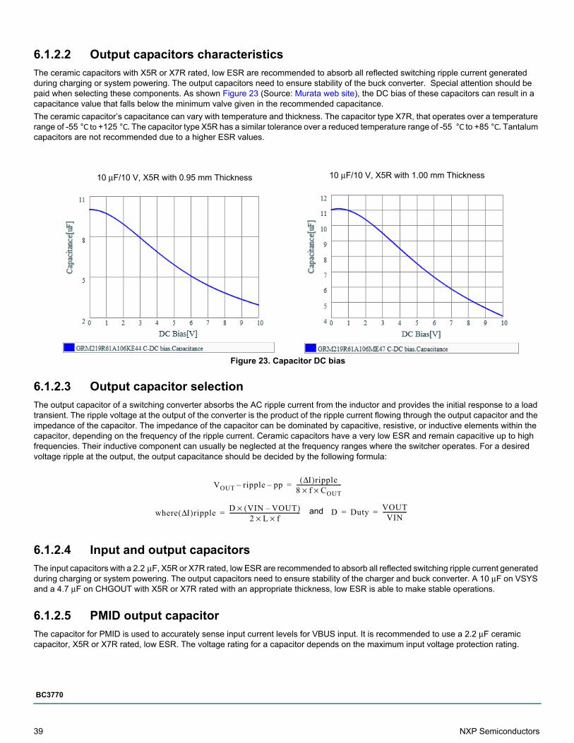
39 NXP Semiconductors
BC3770
6.1.2.2 Output capacitors characteristics
The ceramic capacitors with X5R or X7R rated, low ESR are recommended to absorb all reflected switching ripple current generated during charging or system powering. The output capacitors need to ensure stability of the buck converter. Special attention should be paid when selecting these components. As shown Figure 23 (Source: Murata web site), the DC bias of these capacitors can result in a capacitance value that falls below the minimum valve given in the recommended capacitance.
The ceramic capacitor’s capacitance can vary with temperature and thickness. The capacitor type X7R, that operates over a temperature range of -55 °C to +125 °C. The capacitor type X5R has a similar tolerance over a reduced temperature range of -55 °C to +85 °C. Tantalum capacitors are not recommended due to a higher ESR values.
Figure 23. Capacitor DC bias
6.1.2.3 Output capacitor selection
The output capacitor of a switching converter absorbs the AC ripple current from the inductor and provides the initial response to a load transient. The ripple voltage at the output of the converter is the product of the ripple current flowing through the output capacitor and the impedance of the capacitor. The impedance of the capacitor can be dominated by capacitive, resistive, or inductive elements within the capacitor, depending on the frequency of the ripple current. Ceramic capacitors have a very low ESR and remain capacitive up to high frequencies. Their inductive component can usually be neglected at the frequency ranges where the switcher operates. For a desired voltage ripple at the output, the output capacitance should be decided by the following formula:
6.1.2.4 Input and output capacitors
The input capacitors with a 2.2 μF, X5R or X7R rated, low ESR are recommended to absorb all reflected switching ripple current generated during charging or system powering. The output capacitors need to ensure stability of the charger and buck converter. A 10 μF on VSYS and a 4.7 μF on CHGOUT with X5R or X7R rated with an appropriate thickness, low ESR is able to make stable operations.
6.1.2.5 PMID output capacitor
The capacitor for PMID is used to accurately sense input current levels for VBUS input. It is recommended to use a 2.2 μF ceramic capacitor, X5R or X7R rated, low ESR. The voltage rating for a capacitor depends on the maximum input voltage protection rating.
10 μF/10 V, X5R with 0.95 mm Thickness 10 μF/10 V, X5R with 1.00 mm Thickness
VOUT ripple– pp–IΔ( )ripple
8 f× COUT×--------------------------------=
where IΔ( )rippleD VIN VOUT–( )×
2 L× f×--------------------------------------------------= D Duty
VOUTVIN
-----------------= =and
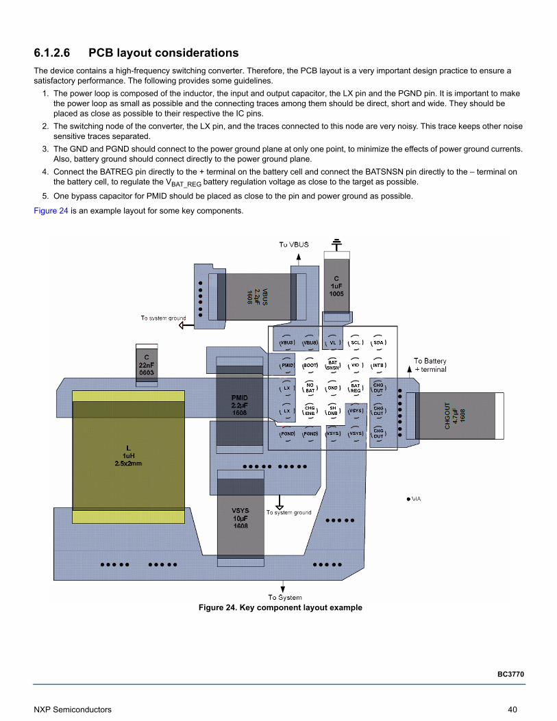
NXP Semiconductors 40
BC3770
6.1.2.6 PCB layout considerations
The device contains a high-frequency switching converter. Therefore, the PCB layout is a very important design practice to ensure a satisfactory performance. The following provides some guidelines.
1. The power loop is composed of the inductor, the input and output capacitor, the LX pin and the PGND pin. It is important to make the power loop as small as possible and the connecting traces among them should be direct, short and wide. They should be placed as close as possible to their respective the IC pins.
2. The switching node of the converter, the LX pin, and the traces connected to this node are very noisy. This trace keeps other noise sensitive traces separated.
3. The GND and PGND should connect to the power ground plane at only one point, to minimize the effects of power ground currents. Also, battery ground should connect directly to the power ground plane.
4. Connect the BATREG pin directly to the + terminal on the battery cell and connect the BATSNSN pin directly to the – terminal on the battery cell, to regulate the VBAT_REG battery regulation voltage as close to the target as possible.
5. One bypass capacitor for PMID should be placed as close to the pin and power ground as possible.
Figure 24 is an example layout for some key components.
Figure 24. Key component layout example
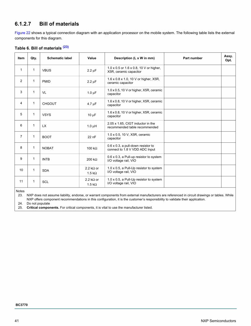
41 NXP Semiconductors
BC3770
6.1.2.7 Bill of materials
Figure 22 shows a typical connection diagram with an application processor on the mobile system. The following table lists the external
components for this diagram.
Table 6. Bill of materials (23)
Item Qty. Schematic label Value Description (L x W in mm) Part numberAssy. Opt.
1 1 VBUS 2.2 μF1.0 x 0.5 or 1.6 x 0.8, 10 V or higher, X5R, ceramic capacitor
2 1 PMID 2.2 μF1.6 x 0.8 x 1.0, 10 V or higher, X5R, ceramic capacitor
3 1 VL 1.0 μF1.0 x 0.5, 10 V or higher, X5R, ceramic capacitor
4 1 CHGOUT 4.7 μF1.6 x 0.8, 10 V or higher, X5R, ceramic capacitor
5 1 VSYS 10 μF1.6 x 0.8, 10 V or higher, X5R, ceramic capacitor
6 1 LX 1.0 μH2.05 x 1.65, CIGT inductor in the recommended table recommended
7 1 BOOT 22 nF1.0 x 0.5, 10 V, X5R, ceramic capacitor
8 1 NOBAT 100 kΩ0.6 x 0.3, a pull-down resistor to connect to 1.8 V VDD ADC Input
9 1 INTB 200 kΩ0.6 x 0.3, a Pull-up resistor to system I/O voltage rail, VIO
10 1 SDA2.2 kΩ or
1.5 kΩ
1.0 x 0.5, a Pull-Up resistor to system I/O voltage rail, VIO
11 1 SCL2.2 kΩ or
1.5 kΩ1.0 x 0.5, a Pull-Up resistor to system I/O voltage rail, VIO
Notes 23. NXP does not assume liability, endorse, or warrant components from external manufacturers are referenced in circuit drawings or tables. While
NXP offers component recommendations in this configuration, it is the customer’s responsibility to validate their application.24. Do not populate25. Critical components. For critical components, it is vital to use the manufacturer listed.
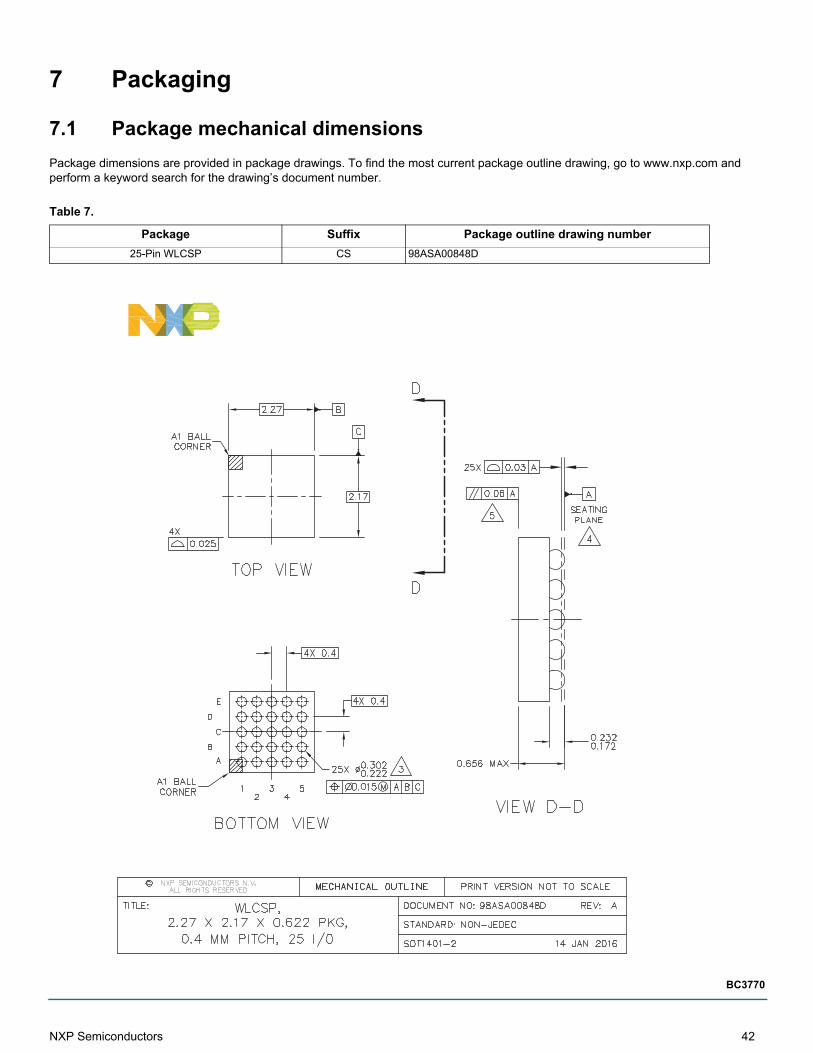
NXP Semiconductors 42
BC3770
7 Packaging
7.1 Package mechanical dimensions
Package dimensions are provided in package drawings. To find the most current package outline drawing, go to www.nxp.com and perform a keyword search for the drawing’s document number.
Table 7.
Package Suffix Package outline drawing number
25-Pin WLCSP CS 98ASA00848D
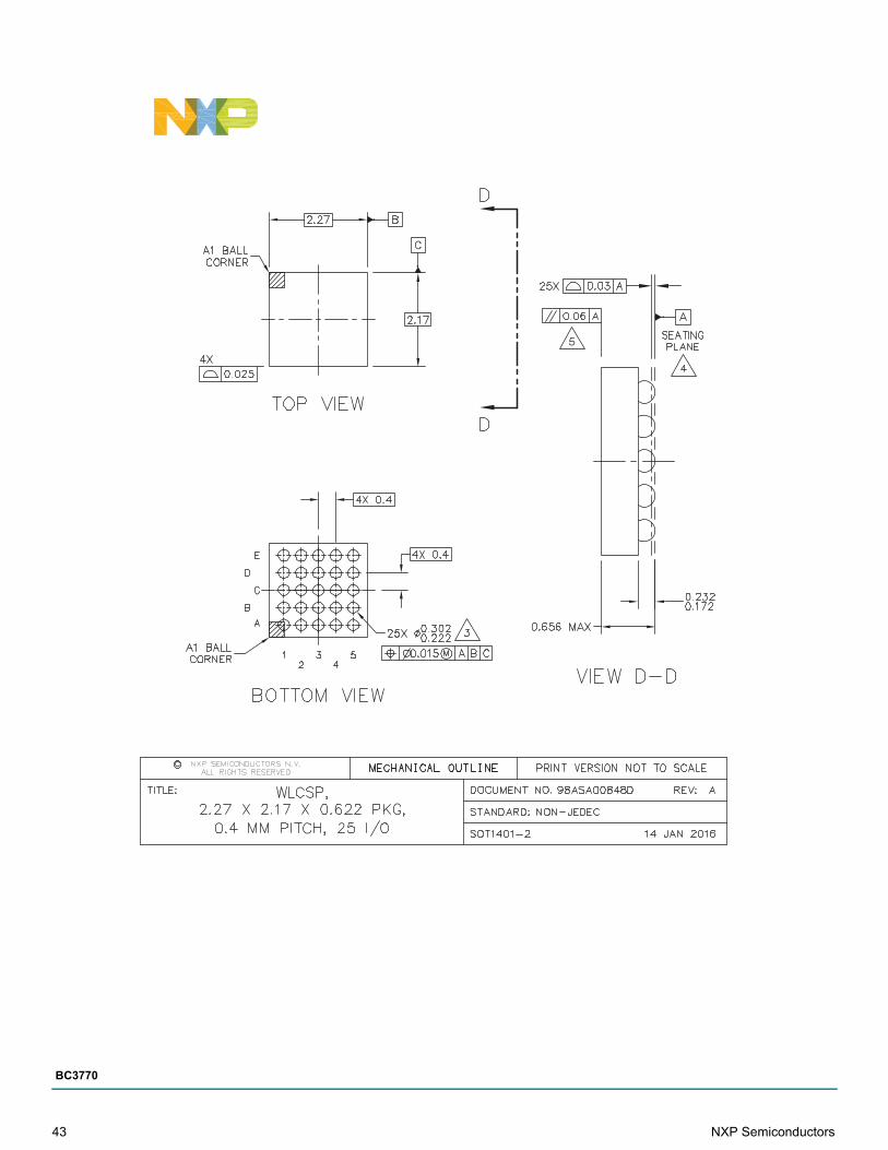
43 NXP Semiconductors
BC3770
NXP Semiconductors 44
BC3770
8 Revision history
Revision Date Description of Changes
1.0
12/2014 • Initial release
2/2015• Corrected Figure 1• Updated Applications on page 1• Corrected typo in Table 2, BC3770 pin definitions
10/2015 • Corrected part number in Table 1, Orderable part variations
7/2016 • Updated to NXP document form and style
Document Number: MC32BC3770Rev. 1.0
7/2016
Information in this document is provided solely to enable system and software implementers to use NXP products.
There are no expressed or implied copyright licenses granted hereunder to design or fabricate any integrated circuits
based on the information in this document. NXP reserves the right to make changes without further notice to any
products herein.
NXP makes no warranty, representation, or guarantee regarding the suitability of its products for any particular
purpose, nor does NXP assume any liability arising out of the application or use of any product or circuit, and
specifically disclaims any and all liability, including without limitation, consequential or incidental damages. "Typical"
parameters that may be provided in NXP data sheets and/or specifications can and do vary in different applications,
and actual performance may vary over time. All operating parameters, including "typicals," must be validated for each
customer application by the customer's technical experts. NXP does not convey any license under its patent rights nor
the rights of others. NXP sells products pursuant to standard terms and conditions of sale, which can be found at the
following address:
http://www.nxp.com/terms-of-use.html.
How to Reach Us:Home Page: NXP.com
Web Support: http://www.nxp.com/support
NXP, the NXP logo, Freescale, the Freescale logo and SMARTMOS are trademarks of NXP B.V. All other product or
service names are the property of their respective owners. All rights reserved.
© 2016 NXP B.V.
Related Documents