Advances in Ceramic Science and Engineering (ACSE) Volume 3, 2014 www.acse-journal.org Nucleation and Growth Mechanisms of Zirconia Film Deposited on Porous Nickel Oxide – Zirconia Substrate by Electron Beam – Physical Vapor Deposition Oleksandr Vasylyev *1 , Mykola Brychevskyi 1 , Iegor Brodnikovskyi 1 , Sergiy Firstov 1 , Mariusz Andrzejczuk 2 , Maciek Spychalski 2 , Małgorzata Lewandowska 2 , Krzysztof Jan Kurzydlowski 2 , Robert Steinberger-Wilckens 3 , Josef Mertens 4 , Jürgen Malzbender 4 1 Frantcevych Institute for Problems of Materials Science, Kyiv, 03680, Ukraine 2 Warsaw University of Technology, Warsaw, 00-661, Poland 3 University of Birmingham, College of Engineering and Physical Sciences, Edgbaston, B15 2TT, UK 4 Forschungszentrum Jülich GmbH, Institute of Energy and Climate Research, 52428 Jülich, Germany *1 [email protected]; 2 [email protected]; 3 [email protected]; 4 jo.mertens@fz- juelich.de Received 21 November, 2013; Revised 10 January, 2014; Accepted 20 January, 2014; Published 18 May, 2014 © 2014 Science and Engineering Publishing Company Abstract The structure of the transitional zone between a zirconia film deposited by EB-PVD and its porous NiO-ZrO2 substrate were studied using transmission and scanning electron microscopy. The plausible condensation mechanisms of zirconia from its vapor phase onto zirconia and nickel oxide phases of the substrate were established. The condensation of zirconia was identified as a two-stage process with two mechanisms of growth, planar and cellular, similar to solidification from the liquid phase. ZrO2 condensation on ZrO2 and NiO phases occurs with different routes. During the planar growth on the ZrO2, the ZrO2 film nucleates and grows up to ~0.3-0.5 µm with no orientation preference as continuous "layer by layer" defective film. The planar ZrO2 film on the NiO of ~0.5-0.7 µm thickness is discontinuous and porous; it consists of oriented structurally perfect "islands". The differences found are probably the result of differences in the melting temperature of ZrO2 and NiO, and Zr and Ni affinities to oxygen as well as their different behavior under high vacuum. The deposition affected zone surrounding the ZrO2 nucleation site is established. Keywords Zirconia Film; Nucleation Mechanism; Growth Mechanism; Thin Structure; Solid Oxide Fuel Cell; Electron Beam – Physical Vapor Deposition Introduction Electron beam – physical vapor deposition (EB-PVD) is a promising process that might enhance the electrochemical performance of solid oxide fuel cells (SOFCs). EB-PVD deposited thin layers contribute to the SOFC lifetime increase and their cost reduction. SOFC based on electrolyte made of zirconia stabilized with 10-mol. % Sc2O3 and 1-mol. % CeO2 (1Ce10ScSZ) deposited by EB-PVD have demonstrated an area specific resistance of ~0.6 ohm·cm 2 at 600 o C and a He leakage rate below 10 -4 mbar·l·cm -2 ·s -1 (Andrzejczuk et al 2012). The conductivity of EB-PVD deposited films on a NiO-8YSZ anode is ~50 % higher than that of layers made with traditional SOFC technology (Vasylyev et al 2009). This high performance is the result of a combination of 1Ce10ScSZ powder, ensuring high electrolyte conductivity, and the electron beam technique, ensuring dense unidirectional nano-sized structure on highly porous NiO-8YSZ anode substrate. Additionally, a strong adhesion of the EB-PVD electrolyte to the anode is achieved, which in itself is a very important prerequisite for high quality SOFCs. The EB-PVD films consist of columns (nanosized 25

Welcome message from author
This document is posted to help you gain knowledge. Please leave a comment to let me know what you think about it! Share it to your friends and learn new things together.
Transcript
Advances in Ceramic Science and Engineering (ACSE) Volume 3, 2014 www.acse-journal.org
Nucleation and Growth Mechanisms of Zirconia Film Deposited on Porous Nickel Oxide – Zirconia Substrate by Electron Beam – Physical Vapor Deposition Oleksandr Vasylyev*1, Mykola Brychevskyi1, Iegor Brodnikovskyi1, Sergiy Firstov1, Mariusz Andrzejczuk2, Maciek Spychalski2, Małgorzata Lewandowska2, Krzysztof Jan Kurzydlowski2, Robert Steinberger-Wilckens3, Josef Mertens4, Jürgen Malzbender4 1Frantcevych Institute for Problems of Materials Science, Kyiv, 03680, Ukraine 2Warsaw University of Technology, Warsaw, 00-661, Poland 3University of Birmingham, College of Engineering and Physical Sciences, Edgbaston, B15 2TT, UK 4Forschungszentrum Jülich GmbH, Institute of Energy and Climate Research, 52428 Jülich, Germany *[email protected]; [email protected]; [email protected]; [email protected]
Received 21 November, 2013; Revised 10 January, 2014; Accepted 20 January, 2014; Published 18 May, 2014 © 2014 Science and Engineering Publishing Company Abstract
The structure of the transitional zone between a zirconia film deposited by EB-PVD and its porous NiO-ZrO2 substrate were studied using transmission and scanning electron microscopy. The plausible condensation mechanisms of zirconia from its vapor phase onto zirconia and nickel oxide phases of the substrate were established. The condensation of zirconia was identified as a two-stage process with two mechanisms of growth, planar and cellular, similar to solidification from the liquid phase. ZrO2 condensation on ZrO2 and NiO phases occurs with different routes. During the planar growth on the ZrO2, the ZrO2 film nucleates and grows up to ~0.3-0.5 µm with no orientation preference as continuous "layer by layer" defective film. The planar ZrO2 film on the NiO of ~0.5-0.7 µm thickness is discontinuous and porous; it consists of oriented structurally perfect "islands". The differences found are probably the result of differences in the melting temperature of ZrO2 and NiO, and Zr and Ni affinities to oxygen as well as their different behavior under high vacuum. The deposition affected zone surrounding the ZrO2 nucleation site is established.
Keywords
Zirconia Film; Nucleation Mechanism; Growth Mechanism; Thin Structure; Solid Oxide Fuel Cell; Electron Beam – Physical Vapor Deposition
Introduction
Electron beam – physical vapor deposition (EB-PVD) is a promising process that might enhance the electrochemical performance of solid oxide fuel cells (SOFCs). EB-PVD deposited thin layers contribute to the SOFC lifetime increase and their cost reduction. SOFC based on electrolyte made of zirconia stabilized with 10-mol. % Sc2O3 and 1-mol. % CeO2 (1Ce10ScSZ) deposited by EB-PVD have demonstrated an area specific resistance of ~0.6 ohm·cm2 at 600 oC and a He leakage rate below 10-4 mbar·l·cm-2·s-1 (Andrzejczuk et al 2012). The conductivity of EB-PVD deposited films on a NiO-8YSZ anode is ~50 % higher than that of layers made with traditional SOFC technology (Vasylyev et al 2009).
This high performance is the result of a combination of 1Ce10ScSZ powder, ensuring high electrolyte conductivity, and the electron beam technique, ensuring dense unidirectional nano-sized structure on highly porous NiO-8YSZ anode substrate. Additionally, a strong adhesion of the EB-PVD electrolyte to the anode is achieved, which in itself is a very important prerequisite for high quality SOFCs. The EB-PVD films consist of columns (nanosized
25
www.acse-journal.org Advances in Ceramic Science and Engineering (ACSE) Volume 3, 2014
diameters and microsized length) and microlamellae; they have a cubic crystalline structure. In addition, the films made of 1Ce10ScSZ powders are doped with Ni and Y due to an interdiffusion of dopants between the anode substrate and the deposited EB-PVD film. The Ni content at the anode – electrolyte interface (AEI) can exceed 2-wt. % that may decrease its conductivity significantly in a course of SOFC operation. An area of EB-PVD film bordering AEI has higher the elasticity modulus than average (Vasylyev et al 2009).
However, one problem that has yet to be solved is the comparatively high gas leakage through zirconia films deposited on porous (>30 %) NiO-ZrO2 substrates. This requires both further elaborations of comparatively thick films deposited on highly porous two-phase (NiO and ZrO2) substrates and comprehensive structural characterization of EB-PVD films. This not only refers to the bulk of a film, but mainly to its interface with the heterogeneous substrate, in order to gain an insight into nucleation and the initial growth stages.
The available literature deals mainly with the nucleation and the growth of thin films deposited on perfect dense substrates. A few models (Volmer-Weber – "island" or 3-d nucleation; Frank-Van der Merwe – ideal epitaxy or "layer by layer"; and mixed model by Stranski-Krastanov, SK Growth) of epitaxial film growth (Movchan et al 1983, Ohring 1992) and four stage microstructural evolution (nucleation, islanding, channel filling, and continuous film growth) based on structural studies of film surfaces at different stages of their growth are well developed (Ohring 1992, Petrov et al 2003), as well as many theoretical models of these processes. As to the structure of thick films, mainly thermal barrier coatings, models developed by Movchan and Demchishin (Movchan et al 1969, 1983), Thornton (Thornton 1977) or their combinations are considered.
In general, for thin films or the initial growth stages of thicker films, it might be concluded that the available knowledge considers the nucleation and growth of films on the substrate surface as a growth of a two-dimensional object on a perfectly homogenous, monocrystalline substrate - like silicon, sapphire or rock salt, which are generally used in the production of different electronic components. The knowledge on thick films deposited on heterogeneous substrates, for instance, thermal barrier coatings, concentrates mainly on the structure of the film bulk and, in particular, the formation of different structure zones in deposited
layers in dependence on substrate temperature, deposition angle, substrate rotation and other technological parameters.
The structure of the substrate-film interface, for unknown reasons, is largely ignored by researchers. There seems to be an assumption that the deposited film adheres to the substrate with some weak forces like that keeps water on a window glass, i.e., with no strong interaction as it can be seen, e.g., in the educational guides to PVD coating.
The purpose of this study is to examine the structural features in the zone of the transition from a porous NiO-8YSZ substrate to a dense EB-PVD 1Ce10ScSZ film, or the zone of the anode-electrolyte interface (AEI), in order to establish the nucleation and growth mechanisms and structural features of electrolyte films formed at electron beam - physical vapor deposition.
Experimental
The 1-mol. % CeO2 – 10-mol. % Sc2O3 – ZrO2 co-deposited powder used in the experiments described here was developed by Prof. Victor Vereshchak and produced at Vil'nohirs'k Mining & Metallurgical Plant, Ukraine. The doping of the zirconia with ~0.5 wt. % SiO2 and ~0.025-wt. % Al2O3, as well as the nano size (20-30 nm) of the initial particles are chemical and structural features of the powder, which insures high electrical conductivity at its SOFC electrolyte application (Vasylyev et al 2011).
Porous (20-25 %) 1Ce10ScSZ cylindrical powder compacts of ∅12-15 mm and 10-15 mm height were prepared with uniaxial pressing and subsequent sintering at 1200 - 1300 °C for 1 hour in air and then used as targets in the EB-PVD process. For deposition, the VU-2M installation (Smorgon, Belarus) operating under hydrocarbon free vacuum (10-5 Pa) was used.
1Ce10ScSZ electrolyte films of 9, 20 and 65 µm thicknesses were deposited. The substrate temperature during the deposition process was either 700 or 900 oC. Samples were annealed for 1.5 hour in air at temperatures in range of 700 to 1200 oC.
Thick (1 to 1.5 mm) porous NiO-8YSZ pellets containing ~30 µm dense electrochemically active NiO-8YSZ anode layer were used as substrates. It could be reasonable to assume that during cooling after the EB-PVD process of applying the electrolyte film a mechanical stress develops in the plane of the AEI due to differences in thermal expansion of electrolyte layer and substrate. This stress might lead
26
Advances in Ceramic Science and Engineering (ACSE) Volume 3, 2014 www.acse-journal.org
to delamination of the electrolyte film from the support. In fact, in-plane stresses are larger for thin films, however, since the fracture is a result of the elastically stored energy; thicker films are more prone to fail due to delamination. The available results suggest an optimum film thickness of ~10 µm, which is chosen mainly based on electrochemical requirements along with the need to obtain a gastight film.
The crystalline structure was studied with X-ray diffraction (XRD) using DRON, Burevestnik, RF.
The structural characterization of the samples was carried out on cross-sections with scanning electron microscopes (SEM, Carl Zeiss CMI SEM LEO 460 and Hitachi SU-70, 2-10 kV). More localized structural investigations were based on scanning transmission electron microscope (STEM, Hitachi HD-2700, 200 kV). The thin foils for STEM investigations were prepared using the Focused Ion Beam (FIB, Hitachi FB 2100) technique.
Results and Discussion
Structure Revealed at a Micron Level
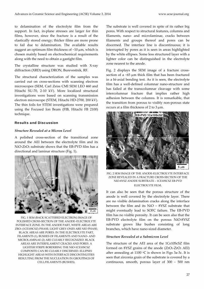
A polished cross-section of the transitional zone around the AEI between the electrolyte film and its NiO-ZrO2 substrate shows that the EB-PVD film has a directional and laminar structure (Fig. 1).
FIG. 1 SEM (BACK SCATTERED ELECTRON) IMAGE OF
POLISHED CROSS-SECTION OF THE ANODE–ELECTROLYTE INTERFACE ZONE. IN THE ANODE PART, WHITE AREAS ARE
ZRO2 (1CE10SCSZ) PHASE; LIGHT GREY ONES ARE NIO PHASE; BLACK AREAS ARE PORES. IN THE ELECTROLYTE PART,
FILAMENTS (1), BUSHES OF FILAMENTS AND NANO- AND MICROLAMINAE (2) ARE CLEARLY RECOGNIZED. BLACK
AREAS ARE INTERFILAMENT CRACKS AND PORES. A LIGHTER STRIPE BORDERING THE NIO-1CE10SCSZ
COMPOSITE CAN BE CLEARLY DISCERNED. ELLIPSES HIGHLIGHT AREAS WITH INTERFACE DISCONTINUITIES RESULTING FROM THE NUCLEATION IN GROUPINGS OF
CELL/FILAMENTS (BUSHES).
The substrate is well covered in spite of its rather big pores. With respect to structural features, columns and filaments, nano- and microlaminae, cracks between filaments and groups thereof and pores can be discerned. The interface line is discontinuous; it is interrupted by pores as it is seen in areas highlighted by the white ellipses. Some less structured layer with a lighter color can be distinguished in the electrolyte zone nearest to the anode.
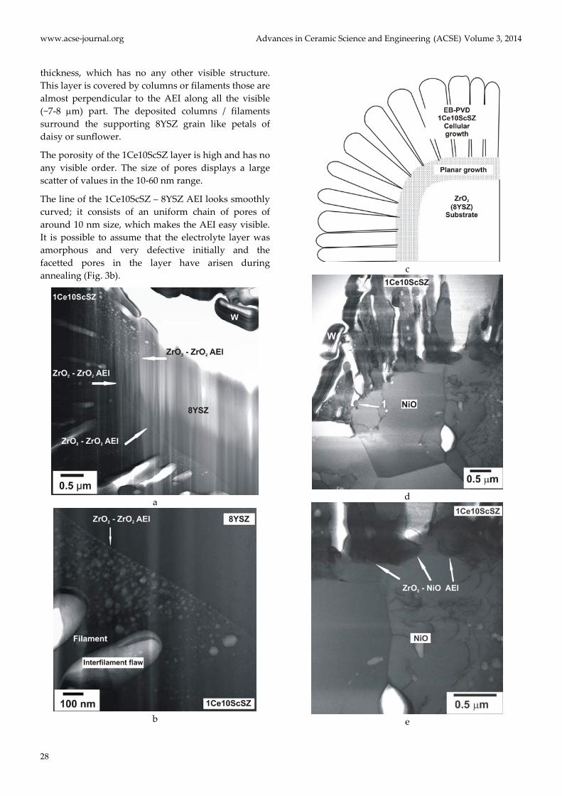
Fig. 2 displays the SEM image of a fracture cross-section of a ~65 µm thick film that has been fractured in a bi-axial bending test. As it is seen, the electrolyte film has a well-defined columnar nano-structure and has failed at the transcolumnar cleavage with some intercolumnar fracture that implies rather high adhesion between the columns. It is remarkable, that the transition from porous to visibly non-porous state occurs at a film thickness of 2 to 3 µm.
FIG. 2 SEM IMAGE OF THE ANODE-ELECTROLYTE INTERFACE
ZONE REVEALED IN A FRACTURE CROSS-SECTION OF THE NIO-8YSZ ANODE SUBSTRATE – 1CE10SCSZ EB-PVD
ELECTROLYTE FILM.
It can also be seen that the porous structure of the anode is well covered by the electrolyte layer. There are no visible delamination cracks along the interface between the film and its NiO – 8YSZ substrate that might eventually lead to SOFC failure. The EB-PVD film has no visible porosity. It can be seen also that the EB-PVD electrolyte film on the porous NiO-8YSZ substrate grows like bushes consisting of long branches, which have nano-sized diameter.
Structure Revealed at a Submicron Level
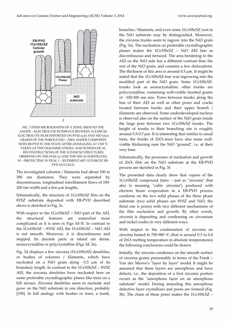
The structure of the AEI area of the 1Ce10ScSZ film formed on 8YSZ grains of the anode (ZrO2-ZrO2 AEI) after annealing at 1100 oC is shown in Figs 3a-3c. It is seen that zirconia grain of the substrate is covered by a continuous, smooth, porous layer of 300 – 500 nm
27
www.acse-journal.org Advances in Ceramic Science and Engineering (ACSE) Volume 3, 2014
thickness, which has no any other visible structure. This layer is covered by columns or filaments those are almost perpendicular to the AEI along all the visible (~7-8 µm) part. The deposited columns / filaments surround the supporting 8YSZ grain like petals of daisy or sunflower.
The porosity of the 1Ce10ScSZ layer is high and has no any visible order. The size of pores displays a large scatter of values in the 10-60 nm range.
The line of the 1Ce10ScSZ – 8YSZ AEI looks smoothly curved; it consists of an uniform chain of pores of around 10 nm size, which makes the AEI easy visible. It is possible to assume that the electrolyte layer was amorphous and very defective initially and the facetted pores in the layer have arisen during annealing (Fig. 3b).
a
b
c
d
e
28
Advances in Ceramic Science and Engineering (ACSE) Volume 3, 2014 www.acse-journal.org
f
FIG. 3 STEM MICROGRAPHS OF A ZONE AROUND THE ANODE – ELECTROLYTE INTERFACE BETWEEN 1CE10SCSZ
ELECTROLYTE FILM DEPOSITED ON 8YSZ (a,b) AND NIO (d,e) GRAINS OF THE POROUS NIO – ZRO2 ANODE COMPOSITE
WITH EB-PVD IN THE STATE AFTER ANNEALING AT 1100 °C TAKEN AT TWO MAGNIFICATIONS, AND SCHEMATICAL
RECONSTRUCTIONS OF THE 1CE10SCSZ STRUCTURES OBSERVED ON THE 8YSZ (c) AND THE NIO (f) SUBSTRATES.
W – PROTECTING W FILM, 1 – RUDIMENTARY 1CE10SCSZ EB-PVD NUCLEUS.
The investigated columns / filaments had about 100 to 300 nm diameters. They were separated by discontinuous, longitudinal interfilament flaws of 100-200 nm width and a few µm lengths.
Schematically, the structure of 1Ce10ScSZ film on the 8YSZ substrate deposited with EB-PVD described above is sketched in Fig. 3c.
With respect to the 1Ce10ScSZ – NiO part of the AEI, the structural features are somewhat more complicated as it is seen in Figs 3d-3f. In contrast to the 1Ce10ScSZ – 8YSZ AEI, the 1Ce10ScSZ – NiO AEI is not smooth. Moreover, it is discontinuous and stepped. Its discrete parts or island are dense, monocrystalline or polycrystalline (Figs 3d, 3e).
Fig. 3d displays a few zirconia (1Ce10ScSZ) dendrites, or bushes of columns / filaments, which have nucleated on a NiO grain along ~3.5 µm of its boundary length. In contrast to the 1Ce10ScSZ – 8YSZ AEI, the zirconia dendrites have nucleated here on some preferable crystallographic planes like trees on a hill terrace. Zirconia dendrites seem to nucleate and grow on the NiO substrate in one direction, probably [100]. In full analogy with bushes or trees, a trunk,
branches / filaments, and even some 1Ce10ScSZ root in the NiO substrate may be distinguished. Moreover, the zirconia trunks seem to ingrow into the NiO grain (Fig. 3e). The nucleation on preferable crystallographic planes makes the 1Ce10ScSZ – NiO AEI line as discontinuous and terraced. The area bordering to the AEI on the NiO side has a different contrast than the rest of the NiO grain, and contains a few dislocations. The thickness of this area is around 0.5 µm. It might be stated that the 1Ce10ScSZ-tree was ingrowing into the modified part of the NiO grain. Some 1Ce10ScSZ-trunks look as monocrystalline; other trunks are polycrystalline, containing well-visible facetted grains of ~100-300 nm size. Pores between trunks along the line of their AEI as well as other pores and cracks located between trunks and their upper branch / filaments are observed. Some underdeveloped nucleus is observed also on the surface of the NiO grain inside the large pore between two 1Ce10ScSZ trunks. The height of trunks to their branching site is roughly around 0.5-0.7 µm. It is interesting that similar to usual trees, the trunks of ZrO2-trees have also some well-visible thickening near the NiO "ground", i.e. at their very base.
Schematically, the processes of nucleation and growth of ZrO2 film on the NiO substrate at the EB-PVD process are sketched in Fig. 3f.
The presented data clearly show that vapors of the 1Ce10ScSZ compound (later – just as "zirconia" that also is meaning "cubic zirconia") produced with electron beam evaporation in a EB-PVD process condense on the two solid phases of the three phase substrate (two solid phases are 8YSZ and NiO, the third one is pores) with two different mechanisms of the film nucleation and growth. By other words, zirconia is depositing and condensing on zirconium and nickel oxides in very different ways.
With respect to the condensation of zirconia on zirconia heated to 700-900 oC (that is around 0.3 to 0.4 of ZrO2 melting temperature in absolute temperatures) the following conclusions could be drawn:
Initially, the zirconia condenses on the smooth surface of zirconia grains presumably in terms of the Frank – Van der Merwe's "layer by layer" model. It might be assumed that these layers are amorphous and have defects, i.e., the deposition of a first zirconia portion occurs as the "amorphous layer on an amorphous substrate" model. During annealing this amorphous defective layer crystallizes and pores are formed (Fig. 3b). The chain of these pores makes the 1Ce10ScSZ –
29
www.acse-journal.org Advances in Ceramic Science and Engineering (ACSE) Volume 3, 2014
8YSZ AEI well visible. Pores are observed across the band of 0.3 to 0.5 µm thickness where no other structural features are visible by TEM. Moreover, there is no visible order in the pore arrangement that could indicate any 3D-island growth. The porous band appears to be non-coherent defective material that is not densified fully even during heat treatment at 1100 oC. In spite of the non-ideal structure of this porous band, it is followed by cells / filaments, which can be seen as evidence that the mechanism of film growth was planar and it might be termed as "defective layer by defective layer".
In terms of the condensation developed for solidification of the liquid phase, the planar growth is realized as perfectly pure material, whose purity is ensured by pushing outwards any alloying elements or impurities at the front of the solid-liquid interface (i.e. the phenomenon of zone refinement, Chalmers 1964).
The solid-liquid interface moves as a planar surface in a direction opposite to the direction of heat removal pushing impurities ahead its front where they are accumulated afterwards. Eventually, their segregated amount may become critical, i.e. enough for the so-called constitutional supercooling that means literally that the thermal supercooling is reached locally for the portion of liquid, which is enriched by the segregating elements in comparison with the pure liquid.
As result, the growth mechanism will be changed. A few new cells / branches / filaments will be nucleated at the solidification front, which will jump ahead due to quick solidification of the enriched liquid portion. The latent heat of fusion will be released at this moment that will result in some stop of the solidification front and redistribution of a new portion of impurities. The planar growth will be replaced by the cellular one since new nuclei will be created and conditions for solidification are changed chemically, or constitutionally. A superposition of at least three physical phenomena namely the thermal supercooling, the fusion latent heat release and the constitutional supercooling occur. It results in structural and chemical heterogeneity, or laminarity, which is well-visible at the micro level in single crystals, metallic welds (Vasilyev 1980) and EB-PVD films as we could observe here (Fig. 1). As an aside, it is generally accepted that some technical instabilities are reasons for the laminar growth.
In full analogy with the solidification of the liquid phase, with the condensation of ZrO2 on a
monocrystalline zirconia substrate (locally, within one ZrO2 grain of porous NiO-ZrO2 composite) heated up to 700-900 oC, we indeed see that zirconia initially condenses according to a planar mechanism and the material grows by "layer by layer" up to about 0.5 µm thickness. The only visible structural feature of the material condensed during this stage is nanosized porosity that is revealed after annealing.
It means that the conditions, which are able to change the EB-PVD film growth mechanism, are reached at the ~0.5 µm film thickness. The planar mechanism is changed by a cellular one. New nuclei are visible. These nuclei transform into cells, which may grow, in our case, as long filaments across all the film thickness. They were nucleated like islands but not on the original ZrO2 substrate (zirconia grain) but the new zirconia film formed by the planar mechanism on the original zirconia substrate.
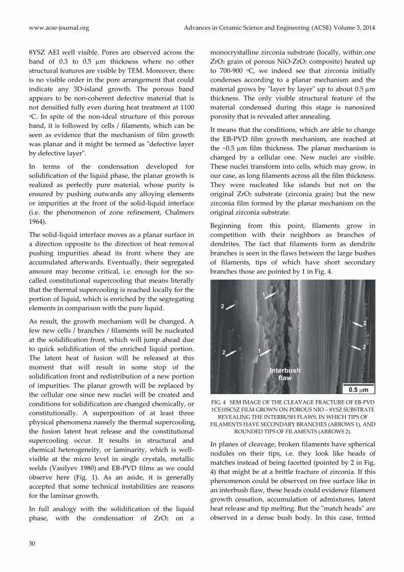
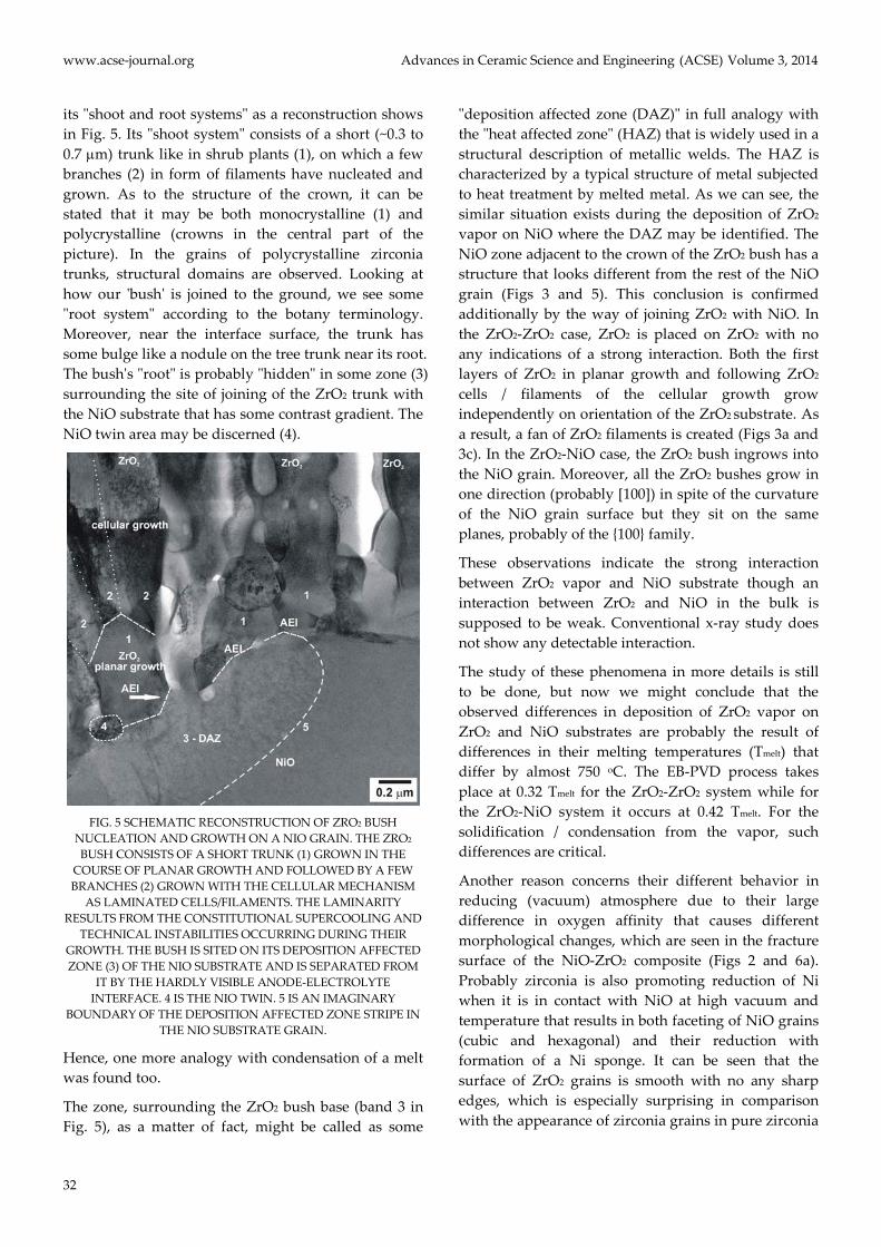
Beginning from this point, filaments grow in competition with their neighbors as branches of dendrites. The fact that filaments form as dendrite branches is seen in the flaws between the large bushes of filaments, tips of which have short secondary branches those are pointed by 1 in Fig. 4.
FIG. 4 SEM IMAGE OF THE CLEAVAGE FRACTURE OF EB-PVD 1CE10SCSZ FILM GROWN ON POROUS NIO – 8YSZ SUBSTRATE
REVEALING THE INTERBUSH FLAWS, IN WHICH TIPS OF FILAMENTS HAVE SECONDARY BRANCHES (ARROWS 1), AND
ROUNDED TIPS OF FILAMENTS (ARROWS 2).
In planes of cleavage, broken filaments have spherical nodules on their tips, i.e. they look like heads of matches instead of being facetted (pointed by 2 in Fig. 4) that might be at a brittle fracture of zirconia. If this phenomenon could be observed on free surface like in an interbush flaw, these heads could evidence filament growth cessation, accumulation of admixtures, latent heat release and tip melting. But the "match heads" are observed in a dense bush body. In this case, fritted
30
Advances in Ceramic Science and Engineering (ACSE) Volume 3, 2014 www.acse-journal.org
appearance of a broken filament tip may evidence a release of energy localized in nano-sized filament due to limited heat dissipation at its deformation before fracture similar to observed spheroids in metallic glasses (Matthews et al 2008).
In the course of their growth, the filaments create their own condensation laminarity, a collective picture of which is clearly seen on the polished cross-sections of bulk samples (Fig. 1). The filaments bend to the vapor flow in order to grow like plants, which bend and turn to the sunlight in order to ensure their growth. As the filament is growing, conditions favoring supercooling may arise again; as a result, secondary filaments will nucleate on the tips of the primary ones.
So, the moment when the filament bush can be formed is approaching. Nevertheless, it has to be kept in mind, that in the very beginning, the cell-filaments arise perpendicularly to the substrate surface, which may result in the formation of a ‘fan’ around the substrate ZrO2 grain as can be seen in Fig. 3a and sketched in Fig. 3c.
The high nano-porosity formed at the stage of planar growth of the ZrO2 layer on the ZrO2 substrate and observed in samples annealed at 1100 oC (Fig. 3b) cannot yet be explained consistently. This porosity might indicate the low density of the initial portions of condensed zirconia in high vacuum that act as reducing agent. The evidence of this may be the well-known fact that as-deposited zirconia coatings look grey, which is always interpreted as a result of an oxygen deficiency. Annealing in air eliminates this deficit; the zirconia film becomes transparent and shines brilliantly. As it can be seen in the TEM, though, this procedure is not able to densify zirconia produced at this stage. The initially deposited zirconia is loose and probably amorphous. It has a lot of defects, which may promote oxygen ionic conductivity. The reasons for this condensation behavior could be the comparatively low temperature of the substrate and, as a result, a high condensation rate. However, the circumstance that a vaporized zirconia deposits on the zirconia substrate, which has some oxygen deficit due to the deep vacuum conditions (we used ~10-5 Pa vacuum free of hydrocarbons) and temperature of 700 oC, is sufficient for the deposited zirconia to lose oxygen. Annealing just recrystallizes pores and makes them visible (defect annealing). Indeed, we see that annealed nanosized pores are well-facetted (Fig. 3b).
In the case of heterogeneous condensation of zirconia
on the nickel oxide substrate, some different
microstructural features can be seen, although the main conclusions on the growth of zirconia films with two (planar and cellular) mechanisms are confirmed here also.
The first distinction is that there is no initial continuous ZrO2 film that could grow with the planar mechanism along the whole surface of the NiO grain (Figs 3d, 3e) as it is observed at the ZrO2 – ZrO2 deposition (Figs 3a-3c). Instead of "one" wide nucleus where the whole zirconia grain serves as the nucleus and zirconia condensates by "layer by layer" at the stage of the planar mechanism, a number of much smaller nuclei can be detected, more than a dozen in our case. It is possible to assume that these nuclei were initiated as "islands" but instead of lateral spreading in order to occupy the entire NiO grain surface, they grow in height. As a result, several separate crystals have been nucleated and grown on each NiO grain.
The second distinction is that the initial part of ZrO2 film grown on the NiO substrate by the planar mechanism has no any visible pores even after annealing (Figs 3d, 3e). As a result, the ZrO2-NiO AEI is hardly visible in comparison with the ZrO2 – ZrO2 AEI.
Considering these features, the only might be concluded that these zirconia crystals are bushes of filaments, which have grown with two mechanisms also – planar and cellular growth. The very short trunk of the bush grows as the planar structure, and the branching filaments grow with the cellular mechanism. As result, no continuous band of planar growth exists. Instead of a band, islands of planar growth covered by a few cell / filaments are observed (Figs 3d-3f). The cells / filaments nucleate as a result of the constitutional supercooling in the frame of each planar island, thus, appearing as trunks of bushes. However, the islands do not spread along the entire NiO grain surface in order to occupy it completely. They had no enough material and time.
Talking about the sites of nucleation and orientation of the ZrO2 bushes on NiO substrates, we may say that they are sited on the curved surface of the NiO grain as terrace (Figs 3 and 5). They cover all the curved grain surface like trees on terraces of a steep hill, i.e. all the bushes have grown in one direction, likely [100], and on the same crystallographic planes, probably the {100} family.
Using the botany terminology, we might say that the ZrO2 bush, which has grown on the NiO substrate has
31
www.acse-journal.org Advances in Ceramic Science and Engineering (ACSE) Volume 3, 2014
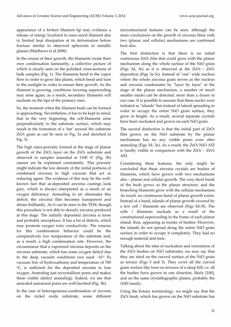
its "shoot and root systems" as a reconstruction shows in Fig. 5. Its "shoot system" consists of a short (~0.3 to 0.7 µm) trunk like in shrub plants (1), on which a few branches (2) in form of filaments have nucleated and grown. As to the structure of the crown, it can be stated that it may be both monocrystalline (1) and polycrystalline (crowns in the central part of the picture). In the grains of polycrystalline zirconia trunks, structural domains are observed. Looking at how our 'bush' is joined to the ground, we see some "root system" according to the botany terminology. Moreover, near the interface surface, the trunk has some bulge like a nodule on the tree trunk near its root. The bush's "root" is probably "hidden" in some zone (3) surrounding the site of joining of the ZrO2 trunk with the NiO substrate that has some contrast gradient. The NiO twin area may be discerned (4).
FIG. 5 SCHEMATIC RECONSTRUCTION OF ZRO2 BUSH
NUCLEATION AND GROWTH ON A NIO GRAIN. THE ZRO2 BUSH CONSISTS OF A SHORT TRUNK (1) GROWN IN THE
COURSE OF PLANAR GROWTH AND FOLLOWED BY A FEW BRANCHES (2) GROWN WITH THE CELLULAR MECHANISM
AS LAMINATED CELLS/FILAMENTS. THE LAMINARITY RESULTS FROM THE CONSTITUTIONAL SUPERCOOLING AND
TECHNICAL INSTABILITIES OCCURRING DURING THEIR GROWTH. THE BUSH IS SITED ON ITS DEPOSITION AFFECTED ZONE (3) OF THE NIO SUBSTRATE AND IS SEPARATED FROM
IT BY THE HARDLY VISIBLE ANODE-ELECTROLYTE INTERFACE. 4 IS THE NIO TWIN. 5 IS AN IMAGINARY
BOUNDARY OF THE DEPOSITION AFFECTED ZONE STRIPE IN THE NIO SUBSTRATE GRAIN.
Hence, one more analogy with condensation of a melt was found too.
The zone, surrounding the ZrO2 bush base (band 3 in Fig. 5), as a matter of fact, might be called as some
"deposition affected zone (DAZ)" in full analogy with the "heat affected zone" (HAZ) that is widely used in a structural description of metallic welds. The HAZ is characterized by a typical structure of metal subjected to heat treatment by melted metal. As we can see, the similar situation exists during the deposition of ZrO2 vapor on NiO where the DAZ may be identified. The NiO zone adjacent to the crown of the ZrO2 bush has a structure that looks different from the rest of the NiO grain (Figs 3 and 5). This conclusion is confirmed additionally by the way of joining ZrO2 with NiO. In the ZrO2-ZrO2 case, ZrO2 is placed on ZrO2 with no any indications of a strong interaction. Both the first layers of ZrO2 in planar growth and following ZrO2 cells / filaments of the cellular growth grow independently on orientation of the ZrO2 substrate. As a result, a fan of ZrO2 filaments is created (Figs 3a and 3c). In the ZrO2-NiO case, the ZrO2 bush ingrows into the NiO grain. Moreover, all the ZrO2 bushes grow in one direction (probably [100]) in spite of the curvature of the NiO grain surface but they sit on the same planes, probably of the {100} family.
These observations indicate the strong interaction between ZrO2 vapor and NiO substrate though an interaction between ZrO2 and NiO in the bulk is supposed to be weak. Conventional x-ray study does not show any detectable interaction.
The study of these phenomena in more details is still to be done, but now we might conclude that the observed differences in deposition of ZrO2 vapor on ZrO2 and NiO substrates are probably the result of differences in their melting temperatures (Tmelt) that differ by almost 750 oC. The EB-PVD process takes place at 0.32 Tmelt for the ZrO2-ZrO2 system while for the ZrO2-NiO system it occurs at 0.42 Tmelt. For the solidification / condensation from the vapor, such differences are critical.
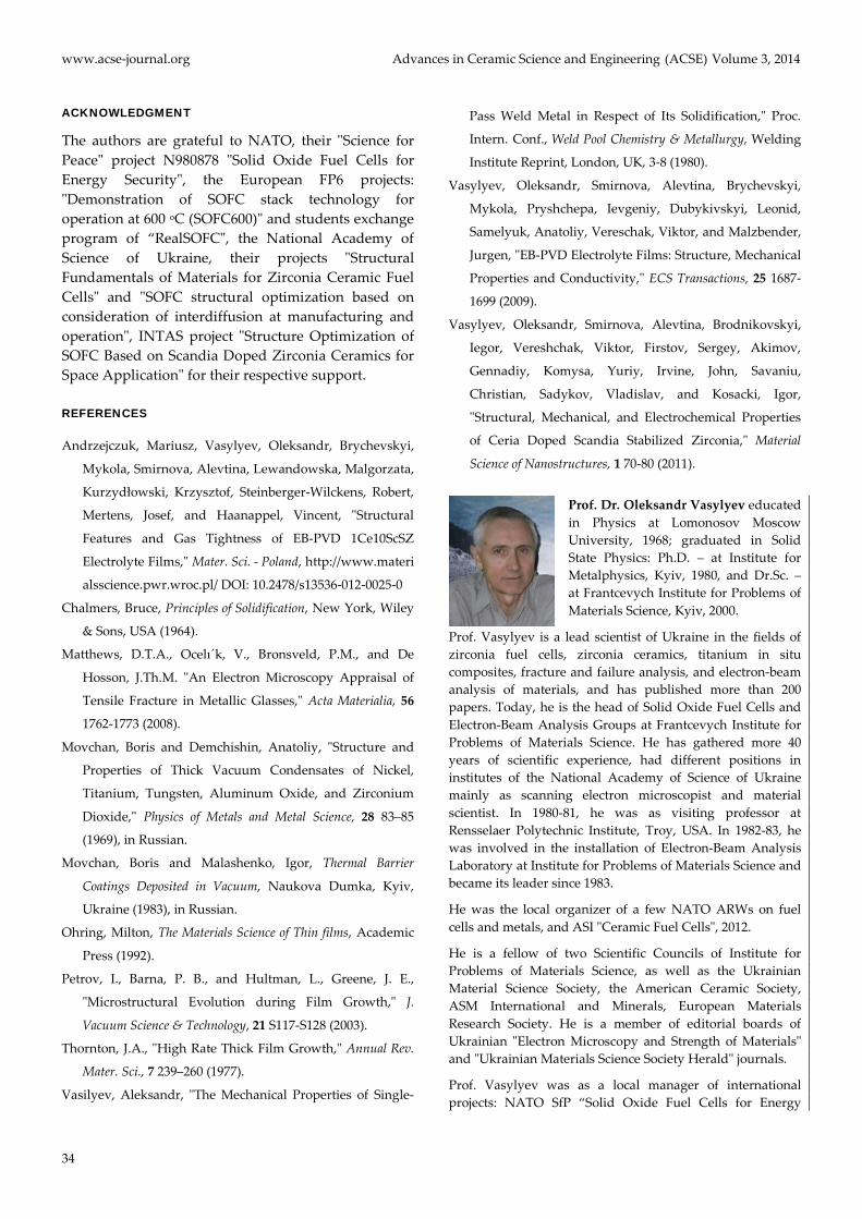
Another reason concerns their different behavior in reducing (vacuum) atmosphere due to their large difference in oxygen affinity that causes different morphological changes, which are seen in the fracture surface of the NiO-ZrO2 composite (Figs 2 and 6a). Probably zirconia is also promoting reduction of Ni when it is in contact with NiO at high vacuum and temperature that results in both faceting of NiO grains (cubic and hexagonal) and their reduction with formation of a Ni sponge. It can be seen that the surface of ZrO2 grains is smooth with no any sharp edges, which is especially surprising in comparison with the appearance of zirconia grains in pure zirconia
32
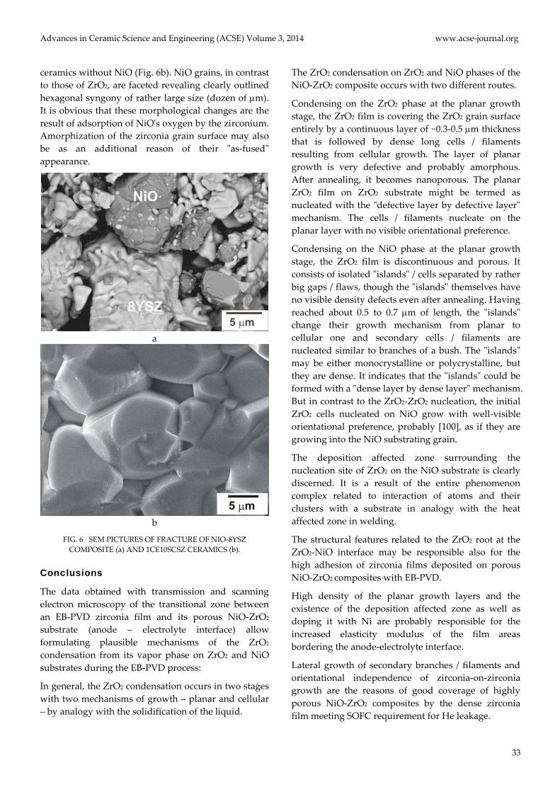
Advances in Ceramic Science and Engineering (ACSE) Volume 3, 2014 www.acse-journal.org
ceramics without NiO (Fig. 6b). NiO grains, in contrast to those of ZrO2, are faceted revealing clearly outlined hexagonal syngony of rather large size (dozen of µm). It is obvious that these morphological changes are the result of adsorption of NiO's oxygen by the zirconium. Amorphization of the zirconia grain surface may also be as an additional reason of their "as-fused" appearance.
a
b
FIG. 6 SEM PICTURES OF FRACTURE OF NIO-8YSZ COMPOSITE (a) AND 1CE10SCSZ CERAMICS (b).
Conclusions
The data obtained with transmission and scanning electron microscopy of the transitional zone between an EB-PVD zirconia film and its porous NiO-ZrO2
substrate (anode – electrolyte interface) allow formulating plausible mechanisms of the ZrO2 condensation from its vapor phase on ZrO2 and NiO substrates during the EB-PVD process:
In general, the ZrO2 condensation occurs in two stages with two mechanisms of growth – planar and cellular – by analogy with the solidification of the liquid.
The ZrO2 condensation on ZrO2 and NiO phases of the NiO-ZrO2 composite occurs with two different routes.
Condensing on the ZrO2 phase at the planar growth stage, the ZrO2 film is covering the ZrO2 grain surface entirely by a continuous layer of ~0.3-0.5 µm thickness that is followed by dense long cells / filaments resulting from cellular growth. The layer of planar growth is very defective and probably amorphous. After annealing, it becomes nanoporous. The planar ZrO2 film on ZrO2 substrate might be termed as nucleated with the "defective layer by defective layer" mechanism. The cells / filaments nucleate on the planar layer with no visible orientational preference.
Condensing on the NiO phase at the planar growth stage, the ZrO2 film is discontinuous and porous. It consists of isolated "islands" / cells separated by rather big gaps / flaws, though the "islands" themselves have no visible density defects even after annealing. Having reached about 0.5 to 0.7 µm of length, the "islands" change their growth mechanism from planar to cellular one and secondary cells / filaments are nucleated similar to branches of a bush. The "islands" may be either monocrystalline or polycrystalline, but they are dense. It indicates that the "islands" could be formed with a "dense layer by dense layer" mechanism. But in contrast to the ZrO2-ZrO2 nucleation, the initial ZrO2 cells nucleated on NiO grow with well-visible orientational preference, probably [100], as if they are growing into the NiO substrating grain.
The deposition affected zone surrounding the nucleation site of ZrO2 on the NiO substrate is clearly discerned. It is a result of the entire phenomenon complex related to interaction of atoms and their clusters with a substrate in analogy with the heat affected zone in welding.
The structural features related to the ZrO2 root at the ZrO2-NiO interface may be responsible also for the high adhesion of zirconia films deposited on porous NiO-ZrO2 composites with EB-PVD.
High density of the planar growth layers and the existence of the deposition affected zone as well as doping it with Ni are probably responsible for the increased elasticity modulus of the film areas bordering the anode-electrolyte interface.
Lateral growth of secondary branches / filaments and orientational independence of zirconia-on-zirconia growth are the reasons of good coverage of highly porous NiO-ZrO2 composites by the dense zirconia film meeting SOFC requirement for He leakage.
33
www.acse-journal.org Advances in Ceramic Science and Engineering (ACSE) Volume 3, 2014
ACKNOWLEDGMENT
The authors are grateful to NATO, their "Science for Peace" project N980878 "Solid Oxide Fuel Cells for Energy Security", the European FP6 projects: "Demonstration of SOFC stack technology for operation at 600 oC (SOFC600)" and students exchange program of “RealSOFC", the National Academy of Science of Ukraine, their projects "Structural Fundamentals of Materials for Zirconia Ceramic Fuel Cells" and "SOFC structural optimization based on consideration of interdiffusion at manufacturing and operation", INTAS project "Structure Optimization of SOFC Based on Scandia Doped Zirconia Ceramics for Space Application" for their respective support.
REFERENCES
Andrzejczuk, Mariusz, Vasylyev, Oleksandr, Brychevskyi,
Mykola, Smirnova, Alevtina, Lewandowska, Malgorzata,
Kurzydłowski, Krzysztof, Steinberger-Wilckens, Robert,
Mertens, Josef, and Haanappel, Vincent, "Structural
Features and Gas Tightness of EB-PVD 1Ce10ScSZ
Electrolyte Films," Mater. Sci. - Poland, http://www.materi
alsscience.pwr.wroc.pl/ DOI: 10.2478/s13536-012-0025-0
Chalmers, Bruce, Principles of Solidification, New York, Wiley
& Sons, USA (1964).
Matthews, D.T.A., Ocelı´k, V., Bronsveld, P.M., and De
Hosson, J.Th.M. "An Electron Microscopy Appraisal of
Tensile Fracture in Metallic Glasses," Acta Materialia, 56
1762-1773 (2008).
Movchan, Boris and Demchishin, Anatoliy, "Structure and
Properties of Thick Vacuum Condensates of Nickel,
Titanium, Tungsten, Aluminum Oxide, and Zirconium
Dioxide," Physics of Metals and Metal Science, 28 83–85
(1969), in Russian.
Movchan, Boris and Malashenko, Igor, Thermal Barrier
Coatings Deposited in Vacuum, Naukova Dumka, Kyiv,
Ukraine (1983), in Russian.
Ohring, Milton, The Materials Science of Thin films, Academic
Press (1992).
Petrov, I., Barna, P. B., and Hultman, L., Greene, J. E.,
"Microstructural Evolution during Film Growth," J.
Vacuum Science & Technology, 21 S117-S128 (2003).
Thornton, J.A., "High Rate Thick Film Growth," Annual Rev.
Mater. Sci., 7 239–260 (1977).
Vasilyev, Aleksandr, "The Mechanical Properties of Single-
Pass Weld Metal in Respect of Its Solidification," Proc.
Intern. Conf., Weld Pool Chemistry & Metallurgy, Welding
Institute Reprint, London, UK, 3-8 (1980).
Vasylyev, Oleksandr, Smirnova, Alevtina, Brychevskyi,
Mykola, Pryshchepa, Ievgeniy, Dubykivskyi, Leonid,
Samelyuk, Anatoliy, Vereschak, Viktor, and Malzbender,
Jurgen, "EB-PVD Electrolyte Films: Structure, Mechanical
Properties and Conductivity," ECS Transactions, 25 1687-
1699 (2009).
Vasylyev, Oleksandr, Smirnova, Alevtina, Brodnikovskyi,
Iegor, Vereshchak, Viktor, Firstov, Sergey, Akimov,
Gennadiy, Komysa, Yuriy, Irvine, John, Savaniu,
Christian, Sadykov, Vladislav, and Kosacki, Igor,
"Structural, Mechanical, and Electrochemical Properties
of Ceria Doped Scandia Stabilized Zirconia," Material
Science of Nanostructures, 1 70-80 (2011).
Prof. Dr. Oleksandr Vasylyev educated in Physics at Lomonosov Moscow University, 1968; graduated in Solid State Physics: Ph.D. – at Institute for Metalphysics, Kyiv, 1980, and Dr.Sc. – at Frantcevych Institute for Problems of Materials Science, Kyiv, 2000.
Prof. Vasylyev is a lead scientist of Ukraine in the fields of zirconia fuel cells, zirconia ceramics, titanium in situ composites, fracture and failure analysis, and electron-beam analysis of materials, and has published more than 200 papers. Today, he is the head of Solid Oxide Fuel Cells and Electron-Beam Analysis Groups at Frantcevych Institute for Problems of Materials Science. He has gathered more 40 years of scientific experience, had different positions in institutes of the National Academy of Science of Ukraine mainly as scanning electron microscopist and material scientist. In 1980-81, he was as visiting professor at Rensselaer Polytechnic Institute, Troy, USA. In 1982-83, he was involved in the installation of Electron-Beam Analysis Laboratory at Institute for Problems of Materials Science and became its leader since 1983.
He was the local organizer of a few NATO ARWs on fuel cells and metals, and ASI "Ceramic Fuel Cells", 2012.
He is a fellow of two Scientific Councils of Institute for Problems of Materials Science, as well as the Ukrainian Material Science Society, the American Ceramic Society, ASM International and Minerals, European Materials Research Society. He is a member of editorial boards of Ukrainian "Electron Microscopy and Strength of Materials" and "Ukrainian Materials Science Society Herald" journals.
Prof. Vasylyev was as a local manager of international projects: NATO SfP “Solid Oxide Fuel Cells for Energy
34

Advances in Ceramic Science and Engineering (ACSE) Volume 3, 2014 www.acse-journal.org
Security” and FP6 SOFC600 "Demonstration of SOFC stack technology for operation at 600 oC", and is of FP7 Nanomat-EPC "Deployment of Societally Beneficial Nano-and Material
Technologies in European Partnership Countries", as well as a few National projects on structural optimization of ceramic fuel cells.
35
Related Documents