NOTICE OF CHANGE MILITARY HANDBOOK RELIABILITY PREDICTION OF ELECTRONIC To all holdersofMIL-HDBK-217F NOT MEASUREMENT SENSITIVE * MIL-HDBK-217F NOTICE 1 10 JULY 1992 EQUIPMENT 1. The following pages of MIL-HDBK-217F have been revised and supersede the pages listed. New Page(s) vii 5-3 5-4 5-7 5-8 5-9 5-1o 5-11 5-12 5-13 5-14 5-19 5-20 6-15 6-16 7-1 7-2 12-3 12-4 A-1 A-2 A-3 A-4 A-5 A-6 A-7 A-8 A-9 A-1 O A-1 1 A-12 A-13 A-14 A-15 A-16 Date Superseded Page(s) Date 2 December 1991 2 December 1991 2 December 1991 2 December 1991 2 December 1991 2 December 1991 2 December 1991 2 December 1991 2 December 1991 2 December 1991 2 December 1991 2 December 1991 2 December 1991 .. 23 5-4 5-7 5-8 5-9 5-1o 5-11 5-12 5-13 5-14 5-19 5-20 6-15 S16 7-1 7-2 12-3 12-4 A-1 A-2 A-3 A-4 A-5 A-6 A-7 A-8 A-9 A-1 O A-1 1 A-12 A-13 A-14 A-15 A-16 2 Deoendxr 19QI 2 Deoe~er 1991 2 December 1991 2 Dece@er 1991 Reprinted without change 2 Decetier 1991 Reprinted without change Reprinted without change 2 Decetier 1991 2 Dece~er 1991 Reprinted without change 2 December 1991 Reprinted without change 2 Decerrber 1991 Reprinted without change Reprinted without change 2 Dece~er 1991 2 December 1991 Reprinted without change Reprinted without change 2 Decenber 1991 2 Dece~r 1991 Reprinted without change 2 Decentxx 1991 2 Deoenber 1991 2 December 1991 2 Decerlber 1991 2 Decerrber 1991 Reprinted without change Reprinted without change 2 Dece~r 1991 2 Decetir 1991 2Dece~er1991 Reprinted without change 2 December 1991 AMSC NIA ~: Approved for public reiease; distribution uniimited. AREA=RELI 1

Welcome message from author
This document is posted to help you gain knowledge. Please leave a comment to let me know what you think about it! Share it to your friends and learn new things together.
Transcript

NOTICE OF CHANGE
MILITARY HANDBOOKRELIABILITY PREDICTION OF ELECTRONIC
To all holdersofMIL-HDBK-217F
NOT MEASUREMENTSENSITIVE*
MIL-HDBK-217FNOTICE 1
10 JULY 1992
EQUIPMENT
1. The following pages of MIL-HDBK-217F have been revised and supersede the pages listed.
New Page(s)vii
5-35-45-75-85-9
5-1o5-115-125-135-145-195-206-156-167-17-212-312-4A-1A-2A-3A-4A-5A-6A-7A-8A-9A-1 OA-1 1A-12A-13A-14A-15A-16
Date Superseded Page(s) Date
2 December 1991
2 December 19912 December 1991
2 December 1991
2 December 1991
2 December 19912 December 1991
2 December 19912 December 1991
2 December 1991
2 December 19912 December 1991
2 December 1991
..
235-45-75-85-9
5-1o5-115-125-135-145-195-206-15S167-17-212-312-4A-1A-2A-3A-4A-5A-6A-7A-8A-9
A-1 OA-1 1A-12A-13A-14A-15A-16
2 Deoendxr 19QI2 Deoe~er 19912 December 19912 Dece@er 1991Reprinted without change2 Decetier 1991Reprinted without changeReprinted without change2 Decetier 19912 Dece~er 1991Reprinted without change2 December 1991Reprinted without change2 Decerrber 1991Reprinted without changeReprinted without change2 Dece~er 19912 December 1991Reprinted without changeReprinted without change2 Decenber 19912 Dece~r 1991Reprinted without change2 Decentxx 19912 Deoenber 19912 December 19912 Decerlber 19912 Decerrber 1991Reprinted without changeReprinted without change2 Dece~r 19912 Decetir 19912Dece~er1991Reprinted without change2 December 1991
AMSC NIA~: Approved for public reiease; distribution uniimited.
AREA=RELI1
MIL-HDBK-217FNOTICE 1
—
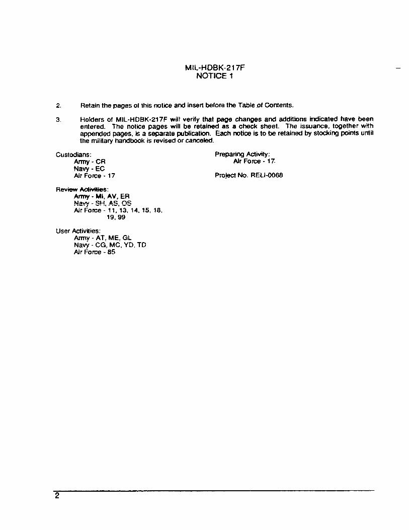
2. Retain the pages of this notice and insert before the Table .of Contents.
3. Holders of MIL-HOBK-217F wilt verify that page changes and additkms indicated have beenentered. The notice pages will be retained as a check sheet. The issuance, together withappended pages, is a separate publication. Each notice is to be retained by stocking points untilthe military handbook is revised or canceled.
Custodians: Preparing Activity:Amly-cR Air Force -17-Navy - ECAh Force-17 Project No. RELI-0088
Review Activities:Army - Ml, AV, ERNavy - SH, AS, OSAir Force -11, 13, 14, 15, 18,
19,99
User Activities:Army - AT, ME, GLNavy - CG, MC, YD, TOAir Force -85

MIL-HDBK-217FNOTICE 1
FOREWORD
MIL-HDBK-217F, Notice 1 is issued to correct minor typographical errors in the basic F Revision. MIL-HDBK-217F (base document) provides the following changes based upon recently completed studies(see Ref. 30 and 32 listed in Appendix C):
1. New failure rate prediction models are provided for the following nine major classesmicrocircuits:
● Monolithic Bipolar Digital and Linear Gate/Logic Array Devices
● Monolithic MOS Digital and Linear Gate/Logic Array Devices
● Monolithic Bipolar and MOS Digital Microprocessor Devices (Including Controllers)
● Monolithic Bipolar and MOS Memory Devices
● Monolithic GaAs Dgital Devices
9 Monolithic GaAs MMIC Devices
● Hybrid Microcircuits
● Magnetic Bubble Memories
● Surface Acoustic Wave Devices
This revision provides new prediction models for bipolar and MOS microcircuits with gate counts up
of
to
60,000, linear microcircuits with up to 3000 transistors, bipolar and MOS digital microprocessor and co-
processor up to 32 bits, memory devices with up to 1 million bits, GaAs monolithic microwave integrated
circuits (MMtCs) with up to 1,000 active elements, and GaAs dgital ICS with up to 10,000 transistors. The
Cl factors have been extensively revised to reflect new technology devices with improved reliability, and
the activation energies representing the temperature sensitivity of the dice (XT) have been changed for
MOS devices and for memories. The C2 factor remains unchanged from the previous Handbook version,
but includes pin grid arrays and surface mount packages using the same model as hermetic, solder-seated
dual in-line packages. New values have been included for the qual~y faaor (~)t the Ieamiw factor (XL)!
and the (MWimnmedal factor (nE). Th8 model for hybrid microcircuits has been revised to be si~ler to
use, to delete the temperature dependence of the seal and interconnect failure rate contributions, and to
provide a method of calculating chip junction temperatures.
2. A new model for Very High Speed Integrated Ckcuits (VHSIC/VHSIC Like) and Very LargeScale Integration (VLSI) devices (gate oounts above 60,000).
3. The reformatting of the entire handbook to make it easier to use.
4. A reduotion in the number of environmental faOtOfS (~E) from 27 to 14.
5. A revised failure rate model for Network Resistors.
6. Revised models for MS and Klystrons based on data supplied by the Electronic IndustriesAssociation Microwave Tube Division.
Supersedes page vii of Revision F vii

MIL-HDBK-217FNOTICE 1
5.1 MICROCIRCUITS, GATE/LOGIC ARRAYS AND MICROPROCESSORS
DESCRIPTION1. Bipolar Devices, Digital and Linear Gate/Logic Arrays2. MOS Devices, Digiial and Linear Gate/Logic Arrays3. Fieid Programmable Logic Array (PLA) and
Programmable Array Logic (PAL)4. Microprocessors
Bi@at Dgital and
DgitalNo. Gates I c,
1 to 100101 to 1,000
1,001 to 3,0003,001 to 10,000
10,001 to 30,00030,001 to 60,000
.0025
.0050
.010
.020
.040
.080
-hear Gate/Logic Array Die Con@exity Failure Rate -Cl
Linear PLA/PALNo. Transistors 1 c, No. (%tes c,
1 to 100 .010 up to 200 .010101 to 300 .020 201 to 1,000 .021301 to 1,000 .040 1,001 to 5,000 .042
1,001 to 10,000 .060
~ Digital and Linear Gate/Logic Array Die Con@exity Failure Rate - Cl”
DgitalNo. Gates
1101
1,0013,001
10,00130,001
to 100to 1,000to 3,000to 10,000to 30,000to 60,000
c,
.010
.020
.040
.080
.16
.29
LinearNo. Transistors I c,
1 to 100 .010101 to 300 .020301 to 1,000 .040
1,001 to 10,000 .060
PLA/PALNo. Gates
up to 500501 to 2,000
2,001 to 5,0005,001 to 20,000
●NOTE: For CMOS gate counts above 60,000 use the VHSICA/t+SIC-Like model in Section 5.3
Die Corr@ex&y Failure Rate -Cl
Bipolar MOSNo. Bits c, c,
UP to 8 .060
Upto 16 .12
lJP to 32 .24
.14
.28
.56I
All Other McParameter
C2
c,
.00085
.0017
.0034
.0068
lel ParametersRefer to
Section 5.8
Section 5.9
Section 5.10
Supersedes page 5-3 of Revision F 5-3

MIL-HDBK-217FNOTICE 1
5.2 MICROCIRCUITS, MEMORIES
DESCRIPTION1. Read Only Memories (ROM)2. Programmable Read Only Memories (PROM)3. LMraviolet Eraseable PROMS (UVEPROM)4. “Flash,- MNOS and Floating Gate Electrically
Eraseable PROMS (EEPROM). Includes bothfbating gate tunnel oxide (FLOTOX) and texturedpotysilicon type EEPROMS
5. Static Random Access Memories (SRAM)6. Dynamic Random Access Memories (DRAM)
Die Complexity Failure Rate - Cl
Merno~ Size, B (Bits)
up to 16K16K<BS64K~K < Bs 256K256K<Bs1M
ROM
.00065
.0013
.0026
.0052
—
EEPROM, DRAMEAPROM
.00085 .0013
.0017 .0025
.0034 .0050
.0068 .010
SRAM(htfos &
BiCMOS)
.0078
.016
.031
.062
Big lar
ROM,PROM
.0094
.019
.038
.075
SRAM
.0052
.011
.021
.042
*’”-’A, Factor for 4 Factor for Xw Cakulation
Total No. of Programmin~ [ 1Total No. ofPmgrarnningCycles Over
EEPROM Life, C
up to 100100< CS2OO200< CS500500< CS1K1K<CS3K3K<CS7K7K<CS15K15K<CS20K20K<CS30K30K<CSIOOKIOOK<CS200K200K < C s 400K400K<CS500K
Flotox ‘
.00070
.0014
.0034
.0068
.020
.049
.10
.14
.20
.681.32.73.4
Textured-
Poly2
.0097
.014
.023
.033
.061
.14
.30
.30
.30
.30
.30
.30
.30
1. Al =6.817x 10⁻⁶ (C)
2. No underlying equation for Textured-Poty.
Cycles Over EEPROM - Textured-Poly A2Life, C
UP to 300K o
300K < C s 400K 1.1
400K < C s 500K 2.3
Atl Other MaParameter
%T
c~
~EI ~) XL
&yC (EEPROMS
onty)
el ParametersRefer to
Section 5.8
Section 5.9
Section 5.10
Page 5-5
~= O For all other devices.
5-4 Su~efsedes page 5-4 of Revision F
9
—
MIL-HDBK-217FNOTICE 1
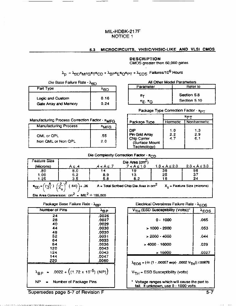
5.3 MICROCIRCUITS, VHSIC/VHSIC-LIKE AND VLSI CMOS
DESCRIPTIONCMOS greater than 60,000 gates
~ = %D%FGnVCD + ~p~E~@FJT + ~~s FaihreW106 Hour.
Die Base Failure Rate - ~D Al Other Model Parameters4
Part Type ‘BDParameter Refer to.
XT Section 5.8Logic and Custom 0.16
Gate Array and Memory~E, ~Q Section 5.10
0.24
1 I 1 Package Type Correction Factor - ~pT#
‘PTManufacturing Process Correction Factor - XMFG I
Package Type Hermetic NonhermeticManufacturing Process ‘MFG
DIP 1.0 1.3
QML or QPL .55 Pii Grkf my 2.2 2.9Chip Carrier 4.7
Non QML or Non QPL6.1
2.0 (Surface Mountb Technology)
Die Corr@exity Correction Factor- ~D-.
r Feature Size I Die An3a (cm*)(Microns) As.4 ,4< As.7 .7< As”l.0- 1.0< As2.O 2.0< A s 3.0
.80 8.0 14 19 38 581.00 5.2 8.9 13 25 371.25 3.5 5.8 8.2 16 24
b-w)(H‘“’4))+”%A = Total ScribedChip Die Area in cmz X~ = Feature Sue (rnicmns)
Die Area Conversion: cm2 = MIL2 + 1!55,000
Pack~e Base Failure Rate - ~p
Nu~r of Pins
2420404448526484
120124144220
—.
‘BP.0026.0027.0029.0030.0030.0031.0033.0036.0043.0043.0047.0060 4
kBp = .0022+ ((1.72X 10⁻⁵) (NP))
NP = Number of Package Pins
Electrical OverStress Failure Rate - kac
VTH (ESD SUSC8@bll~ (vOkS))*
o- 1000
>1000-2000
>2000-4000
>4000- 16000
> 1600C)
~‘EOS
.065
.053
.044
.029
.0027
~S = (-In (1 -.00057 exp(- .0002 V~)) /.00876
VW= ESD Susceptibility (volts)
“ Vottage ranges whch will cause the part tofail. If unknown, use O -1000 votts.
Supersedes page 5-7 of Revision F 5“7

MIL-HDBK-217F
5.4 MICROCIRCUITS, @As MMIC AND DIGITAL DEVICES
DESCRIPTIONGallium Arsenide Mimwave Monolithic Integrated Circuit(~- MMIC) and &As ~d hte(jmted Ciiuits lkw
MESFET Transistors and Gold Based Metallization
~= [ cl~~A + C2nE J7cL~ FailuresH06 Hours
w: Die Complexity Faihre Rates - c,/
Complexity c,(No. of Eiements) 1
1 to 100 4.5101 to 1000 7.2
1. Cl accounts for the folbwing active
elements: transistor, diodes.
m: Die Complexity Failure Rates - Cl
Complexity c,(No. ofElements)
1 to 1000 251,001 to 10,000 51
1. Cl aocounts for the following active
elements: transistors, diodes.
Device Application Factor - Xi.Application
MMIC -S
Low NokBe&b wPower(sloornw)
Driver &Hi@ POwer(>100mW)Unknown
Digital DevicesAll Dgital AppIiitions
1.03.03.0
1.0
All Other Model ParametersParameter Refer to
%T S-ion 5.8
c~ Section 5.9
~E, XL, ~Q Section 5.10
5-8

MIL-HDBK-217FNOTICE 1
5.5 MICROCIRCUITS, HYBRIDS
DESCRIPTIONHybrid Microcircuits
Nc = Number of Each Particular Corrpnent
kc = Failure Rate of Each Particular Component
The general procedure for cfevebping an overall hybrid failure rate is to calculate an individual faiiure ratefor each cmmponent type used in the hybrid and then sum them. This summation is then modified toaccwnt for the overall hybrid function (%F), screening tevel (~), and maturity (XL). The hybrid package
failure rate is a function of the active component failure modified by the environmental faCtOf (i.e., (1 + .2~E) ). Onty the conpment types listed in the following table are oonsk%md to contribute significantly to
the overall failure rate of most hybrids. All other component types (e.g., resistors, inductors, etc.) arecxmsidered to contribute insignificantly to the overall hybrid failure rate, and are assumed to have a failurerate of zero. This simplifkxtion is valid for most hybrids; however, if the hybrid consists of mostiy passivecomponents then a failure rate should be calculated for these devices. If factoring in other componenttYp& aSWme ma = 1,XE =1 and TA = Hybrid Case Temperature for these calculations.
Determination of X.
Determine Ac for These
Component Types
Micmcircults
Discrete Semiconductors
Capacitors
Handbook Section
5
6
10
Mak; These Assumptions When Determining
‘c
C2=0, ~Q=l, ~L = 1, TJ as Determined from
Section 5.12, ~P = O (for VHSIC),
nE = 1 (fOr SAW).
XQ = 1, TJ as Determined from Section 6.14,
~E=l.
%=l’TA = Hybrid Case Temperature,
RE=l.
NOTE: tf maxirrwrn rated stress for a die is udumwn, assume the same as for a discretely packagedie of the same type. If the same die has several ratings based on the discrete packagedtype, assume the lowestrating.Power rating used should be based on case temperaturefor discrete semiconductors. -
Circuit Functbn Faotor - %F
Circuit Type I ~F I
Digital 1.0
Video, 10MHz<f<l GHz 1.2
Micruwave, f >1 GHz 2.6
Linear, f <10 MHz 5.8
Power 21
All Other Hybrid Model Parameters
XL, ~Q, ~E Refer to Section 5.10
Supersedes page 5-9 of Revision F 5-9.
MIL-HDBK-217F
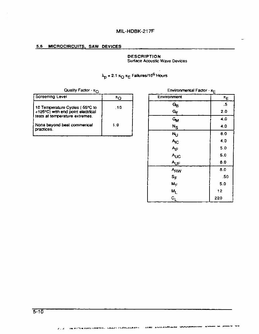
5.6 MICROCIRCUITS, SAW DEVICES
Quality Factor - ZO
Screening Level
10 Temperature Cycles (-55~ to+1250C) with end point electricaltests at temperature extremes.
None beyond best cornrnerkalpractioes.
DESCRIPTIONSurface Acoust”k Wave
~ = 2.1 XQ ZE Failures/106 Hours
7CQ
.10
1.0
Environmental Faotor -xcL
Environment ~E
% .5
GF 2.0
% 4.0
Ns 4.0
Nu 6.0
Alc 4.0
‘IF 5.0
%c 5.0
‘UF 8.0
‘RW 8,0
SF .50
lul~ 5.0
ML 12
CL 220
MIL-HDBK-217F
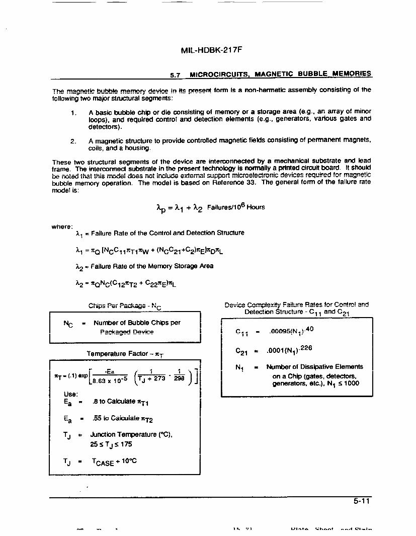
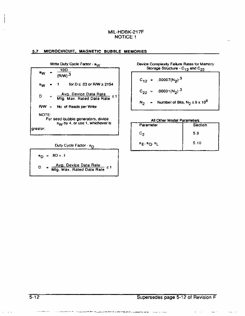
5.7 MICROCIRCUITS, MAGNETIC BUBBLE MEMORIES
The magnetic bubble memory device in its present form IS a non-hermetic assembly mnsisting of thefollowing two major structural segments:
1. A basic bubble chip or die consisting of memory or a storage area (e.g., an array of minorloops), and required control and detection elements (e.g., generators, various gates anddetectors).
2. A magnetic structure to provide contmlied magnetic fields consisting of permanent magnets,coiis, and a housing.
These two structural segments of the device are interconnected by a meohanioai substrate and leadframe. The interconnect substrate in the present technology is norrnaily a prtnted circuit board. It shouldbe noted that this modei does not inciude extemai support rnioroeiectronic devices required for magneticbubbie memory operation. The rrmdei is based on Reference 33. The generai form of the failure ratemodel is: -
~= Al + ~~ Faii.re#106Wum
where:x, = Faiiure Rate of the Control and Detection Stmcture
xl = ~Q [~cc 11 ~Tl ~w + (NCC21 +c2)@~D~L
~. Failure Rate of the Memory Storage Area
Chips Per Package - Nc
I %= Number of Bubble Chips per
Packaged Device
Temperature Factor - ~T
[
-Ea
(
1 1%T=(.1)8W
8.63 x 10⁻⁵ TJ +273-%6 )1Use:Ea = .8 to Calculate %~1
Ea = .= to Catiiate %T2
TJ = Junctbn Teqxwature (W),
25$ TJS 175
TJ = TCASE + 10”C
Device Complexity Faiiure Rates tor Contmi andDetection Structure - Cl 1 and C21
c,, == .00095 (N1).40
c~, = .0001 (N1)”226
N, = Number of Dissipative Elements
on a Chip (gates, detectors,generators, etc.), N1 s 1000
,
I
MIL-t+DBK-217FNOTICE 1
5.7 MICROCIRCUIT, MAGNETIC BUBBLE MEMORIES
Write Duty Cycle Factor - ~
XW
Icw
D
[Uu
(q.3
1 for Ds.030r RAN22154
Avg. Device Data Rate <,Mfg. Max. Rated Data Rate -
No. of Reads per Write
NOTE:For seed-bubble generators, divide
nw by 4, or use 1, whichever is
jreater.
Duty Cycle Factor - ZD
q) = .9D + .1
D=Avg. Device Data Rate <,
Mfg. Max. Rated Data Rate -
Device Ccm@exity Failure Rates for MemoryStorage Structure - Cl 2 and C22—
C,* = .00007 (N2)”3
C*Z = .00001 (N2)-3
N2 = Number of B~s, N2s 9 x 10⁶
Atl Other Model ParametersParameter Section
c~ 5.9
~E, ~Q, XL 5.10
5-12 Supersedes page 5-12 of Revision F
MIL-HDBK-217FNOTICE 1
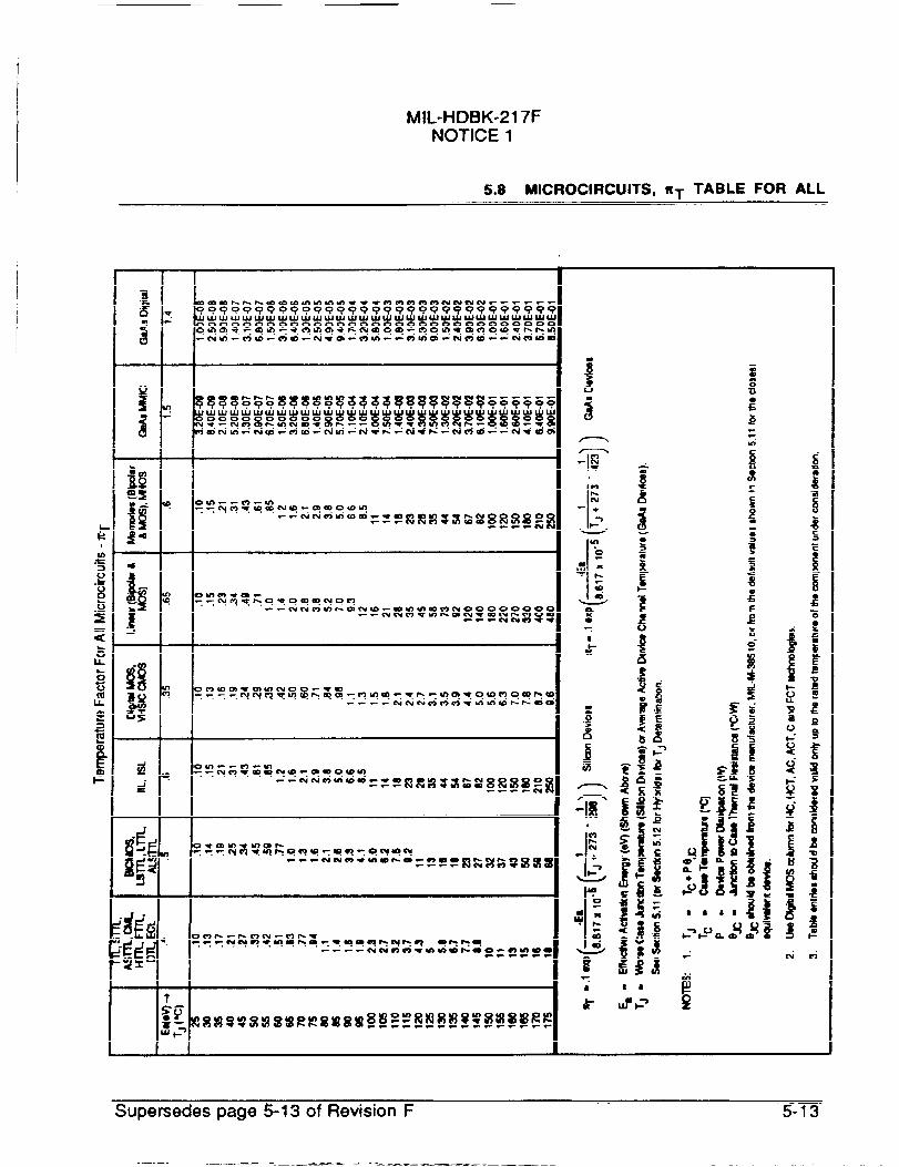
5.8 MICROCIRCUITS, %T TABLE FOR ALL
-In
IT I k
Supersedes page 5-130f Revision F 5-13

MIL-HDBK-217F
5.9 MICROCIRCUITS, C9 TABLE FOR ALL
Package Failure Rate for all Microcircuits - C2
Packaaa Tvoe—.— -- —Hermetic: DIPs
w/Solder or Norlhermetic:Number of Weld Seal, Pin DIPs with Glass Flatpacks with Cans4 DIPs, PGA,Functional Grid Army SeaF Axial Leads on SMT (Leaded
Pins, Np (PGA)l , SMT 50 Mil Centers3 and
(Leaded and Nonleaded)5Nonleaded)
3 .00092 .00047 .00022 .00027 .00124 .0013 .00073 .00037 .00049 .0016
.0019 .0013 .00078 .0011 .0025: .0026 .0021 .0013 .0020 .003410 .0034 .0029 .0020 .0031 .004312 .0041 .0038 .0028 .0044 .005314 .0048 .0048 .0037 .0060 .006216 .0056 .0059 .0047 .0079 .007218 .0064 .0071 .0058 .008222 .0079 .0096 .0083 .01024 .0087 .011 .0098 .01128 .010 .014 .01336 .013 .020 .01740 .015 .024 .01964 .025 .048 .03280 .032 .041128 .053 .068180 .076 .098224 .097 .12
1. C2=2.8 X 10⁴ (N$ 1“W 2. C2 = 9.0 x 10⁻⁵ (NP)’ .5’
3. Cz = 3.0 x 10⁻⁵ (N$l .82 4. Cz = 3.0 x 10⁻⁵ (N$2.01
5. C2=3.6 X 10⁴ (N$’”m
NOTES:
1. SMT: Suffaoe Mount Tectmdqy
2. DIP: Dual h!-ine Pm
3. tf DIP Seal type is urWmwn, a8stmm @ass
4. m pacbge fabe rate (C2) aooounts for failures associated only with the package itself.
Fallums associated with mounting the package to a cimutt board are acoounted for inSection 16, Interconnection AsseMies.
5“14
MIL-HDBK-217FNOTICE 1
5.12 MICROCIRCUITS, TJ DETERMINATION, (FOR HYBRIDS)
. Jr —. . -, ---- -- --------------
Conductivity,Typkal Feature Ki
Material Typical Usage Thiikness, From Figure ()()1 ~i
() (
W/in2Ki
+ (In.) 5-1Vln in2 QC/W
Silicon Chip Device 0.010 A 2.20 .0045
Chip Devioe 0.0070 A .76 .0092
Au EuWctic Chip Attach 0.0001 B 6.9 .000014
Solder Chip/Substrate Attach 0.0030 B/E 1.3 .0023
Epoxy (Dielectric) Chip/Substrate Attach 0.0035 B/E .0060 .58
Epoxy (Conductive) Chip Attach 0.0035 B .15 .023
mid Fih Dielectric Glass Insulating Layer 0.0030 c .66 .0045
Alumina Substrate, MHP 0.025 D .64 .039
Beryllium Oxide Substrate, PHP 0.025 D 6.6 .0038
Kovar Case, MHP 0.020 F .42 .048
Aluminum Case, MtiP 0.020 F 4.6 .0043
Copper Case, PHP 0.020 F 9.9 .0020
NOTE: MHP: Muttichip Hybrid Package, PHP: Power Hybrid Package (Pwr: z 2W, Typically)
n = Number of Material Layers
Ki =()
W/in*Thermal conductivity of ith Material ~ (User Pmided or From Tabie)
L, - “Thuhess of ith Matehal (in) (User Provided or Fmrn TabIe)
A= D& Ama (#). If Die Area cannot be readlfy determined, estimate as fotkws:
A= [ .00276 (No. of Die Adhte Wire Terminals)+ .041~
Estimate TJ as Follows:
TJ = Tc + (e~ (p~
Tc =
eJ~ =
PD =
Hybrid Case Temperature (~). ff unknown, use the Tc Default Table shown in Section 5.11.
Junction-to-Case Thermal Resistance (°C/W) (As determined above)
Die Power Dissipatbn (W)
Supersedes page 5-19 of Revision F 5-19

MIL-HDBK-217F
5.13 MICROCIRCUITS, EXAMPLES
Example 1: CMOS Digftal Gate Array
Given: A CMOS digital timing chip (4046) in an airborne inhabited argo application, case temperature48”C, 75mW power dissipation. The device k prwured with normal manufacturers screeningconsisting of temperature cycJing, constant acceleration, electrical testing, seal test and externalvisual inspection, in the sequence given. The component manufacturer also performs a B-levelbum-in followed by electrical testing. All screens and tests are performed to the applicable MIL-STD-883 screening methd. The pakage is a 24 pin ceramic DIP with a glass seal. The devicehas been manufactured for several years and has 1000 transistors.
Section 5.1
c1 = .020
XT = .29
c~ = .011
nE = 4.0
~Q = 3.1
1000 Transistor -250 Gates, MOS Cl Table, Digital Column
Determine TJ from -ion 5.11
TJ = 48°C + (28°C/W)(.075W) = 50”C
Determine XT from s~ion 5.8, Digital MOS ~mn.
Section 5.9
Section 5,10
Section 5.10
Group 1 TestsGroup 3 Tests (B-1evel)TOTAL
50 Pointso~
80 Points
XL = 1 Section 5.10
~= [ (.020)(.29) + (.011) (4)] (3.1)(1) -.15 Failure/106 Hours
Example 2: EEPROM
Given: A 128K Fiotox EEPROM that is expeoted to have a TJ of 80”C and experience 10,000
reacVwrite cycles over the life of the system. The part k procured to all requirements ofParagraph 1.2.1, MIL-STD-863, Class B screening level requirements and has been ina~n for three years- H ~ ~a~ in a 28 @n DIP with a glass seal and will be USed in artairborne uninhabtied cargo application.
~=(cl~T+c2w+*)mfiL Section 5.2
c, = .0034 Section 5.2
%T = 3.8 Section 5.8
C2 - .014 Section 5.9
tI
MIL-HDBK-217FNOTICE 1
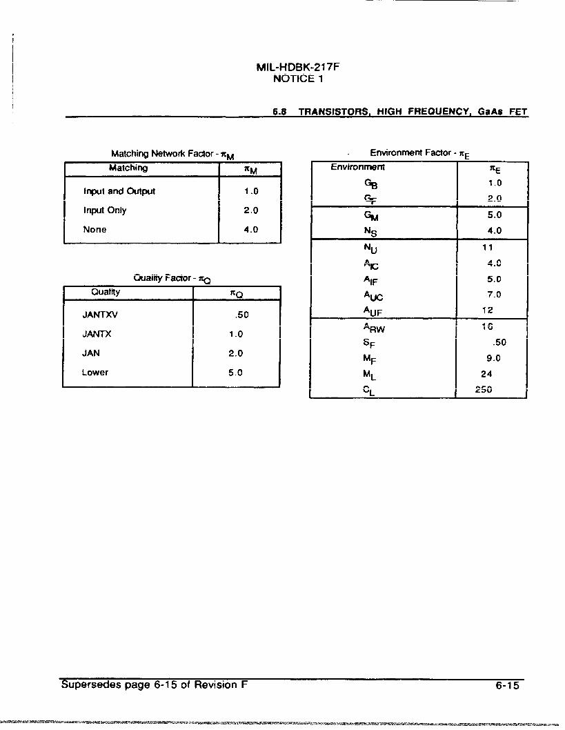
6.8 TRANSISTORS, HIGH FREQUENCY, GaAs FET
Matching Network Factor - XM
Matching
Inputand Output 1.0
Input Only 2.0
None 4.0
Qualtty Fac?or - ~
Quality
JANTXV
MN-rx
JAN
Lower
.50
1.0
2.0
5.0
. Environment Factor - XCL
Envkonrnent ~E
% 1.0
% 2.0
%t 5.0
Ns 4.0
Nu 11
AC 4.0
‘IF 5.0
Am 7.0
‘UF 12
‘RW 16
SF .50
MF 9.0
ML 24
C’ 250
Supersedes page 6-15 of Revision F 6-15
MIL-HDBK-217F
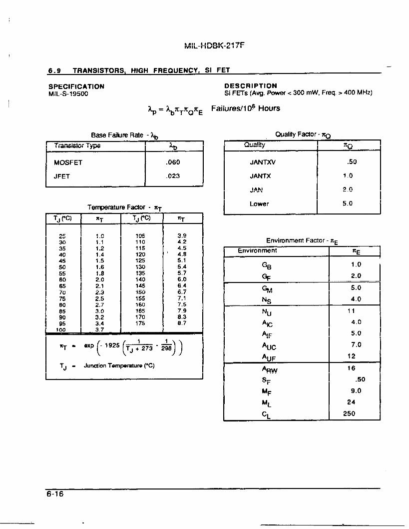
6.9 TRANSISTORS, HIGH FREQUENCY, S1 FET
SPECIFICATIONMIL-S-19500
Base Failure Rate - ~
I MOSFET
I.060
IJFET .023
h \
Temperature Factor - XT
TJ (oC) %T TJ (“C) XT
25 1.0 105 3.930 1.1 110 4.235 1.2 115 4.540 1.4 120 ‘ 4.845 1.5 125 5.150 1.6 130 5.455 13560 ;:: 140 :::65 2.1 145 6.470 2.3 15075 2.5 155 H80 2.7 160 7.585 3.0 165 7.990 3.2 170 8.395 3.4 175 0.7
100 3.7
((
1%T = exp
))
-1925 q; 273 - ~
TJ - Junckn Temperature (°C)
DESCRIPTIONSi F=s (Avg. Power< 300 mW, Freq. >400 Mliz)
Failures/l 06 Hours
Quality Factor - ~
Quality YCQ
JANTXV .50
JANTX 1.0
JAN 2.0
Lower 5.0
Environment Factor - xc
Environment
GB
*
Nu
Ac
‘IF
‘Uc
‘UF
&w
SF
MF
ML
c,
1.0
2.0
5.0
4.0
11
4.0
5.0
7.0
12
16
.50
9.0
24
250
MIL-HDBK-217F
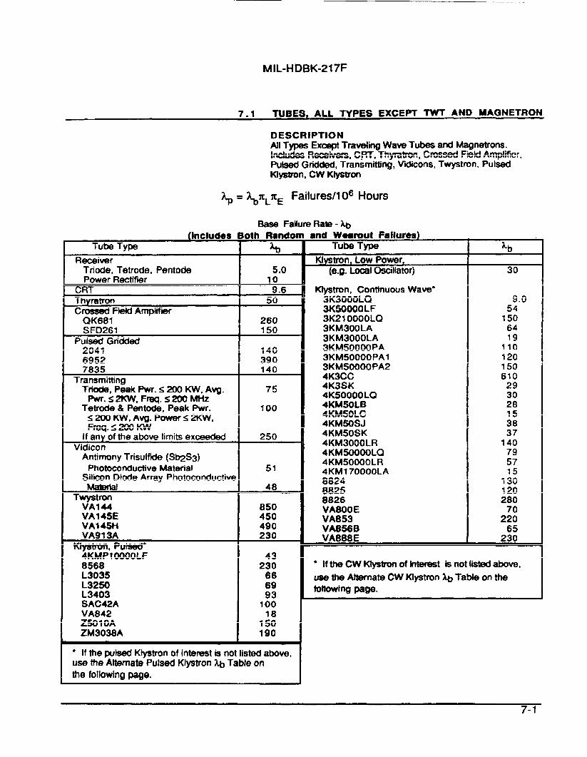
7.1 TUBES, ALL lYPES EXCEPT T’WT AND MAONETRON
DESCRIPTIONAll Types Except Traveling Wave Tubes and Magnetrons.Includes Rece’hmm, CORT,Thyratron, Crossed F@ld Amplifier,Pulsed Gridded, Transmitting, Vidicons, Twystron, PukedKlystron, CW KJystron -
b= %XL%Failures/l OGHours
Base FaWe Rate - ~(Includes Both Rafbdof
Tube Type bReceiver
Triode, Tetrode, Pentode 5.0Power Rectifier 10
CRT I Oc
ThyratmCrossed Fi@d AmPtifief I
QK681 ‘ I 260SFD261 150
Pulsed Gridded2041
I140
6952 3907835
Tra;$rnittingTnode, Peak Pwr. s 200 KW, Avg.
Pwr. s2KW, Freq. S200MHzTetrode & Pentode, Peak Pwr.
5200 W, Avg. Powers 2KW,Freq. s200KW
If any of the above limits exceededVidicon
Antimony Trisulfide (Sb2S3)
140
75
100
250
Photoconductive MaterialI
51Silicon Diode Array Photoconductive
Maledal -Twystron
VA144VA145EVAI 45HVA913A
Klystron, ~UkOCf*4wtf WOOOLF8568L3035L3250L3403SAC42AVA842Z501 OAZM3038A
48
850450490230
43230
666993
10018
150190
c If the pulsed Klystron of interest is not listed above,use the Altamate Pulsed Klystron ~ Table onthe following page.
and We@rout Faltures)Tube Type
Klystron, Low Power,(e.g. Local OscNator)
Klystron, Continuous Wave*3K3000LQ3K50000LF3K21 0000103KM300LA3KM3000LA3KM50000PA3KM50000PA13KM50000PA24K3CC4K3SK4K50000LQ4KM50LB4KM50LC4KM50SJ4KM50SK4KM3000LR4KM50000LQ4KM50000LR4KM170000LA882488258826VA800 EVA853VA856BVA888E
9.054
1506419
110120150610
293028153837
140795715
130120280
70220
65230
● If the CW Klystron of fntemst k not listed above,
uae the Alternate CW Klystron ~ Table on thefollowing page.
/-1

..
MIL-HDBK-217FNOTICE 1
7.1 TUBES, ALL TYPES EXCEPT IWT AND MAGNETRON
Alternate” Base Failure Rate for Pulsed Klystrons - A
F(GHz))@fw) .2 .4 .6 .8 1.0 2.0 4,0 6.0
.01 16 16 16 16 16 16 16 16
.30 16 16 17 17 17 10 20 21
.80 16 17 17 18 18 21 25 3017 17 18 18 19 22 28 34
$: 18 20 21 23 25 34 515.0 19 22 25 28 31 45 758.0 21 25 30 35 40 63 1100 2228 34 40 45 755 31 45 60 75 90 180
%)” 2.94 (F)(P) + 16
F . Operating Frequency in C3HZ,0.2s Fs 6
P- Peak Output PowerIn MW, .01 s P ~ 25 andP s 490 F-2.95
“Sea previouspage for other Klystron Base FailureRates.
Atternate* Base Fatture Rate for CW K@tr’ona - ~
F(MHz)P(KW) 300 500 8001000 2000 4000 6000 800C
0.1 30 31 33 34 38 47 57 6632 33 34 39 48 57 66
$; :; 333435 40 49 585.0 33 34 35 36 41 508.0 34 35 37 38 42
10 35 3638394330 4550 :H:80 E 71 73
100 80 81
%- 0.5P + .aM6F + 29
P = Average Output Power in KW, O.ls Ps 100
and P s 6Lqlo)6(F)-’ .7F = OpamtingFrequencyin MHz.
300s Fs8000
“Sao pr.vious page for other Ktystmn Base FailureRates.
Learning Factor - X[
“T (years) ‘L
<1 10
2 2.3
23 1.0
10(T) -2”’, 1 sT<3~L =w IO, Ts1= 1,T23
T = Number of Years since introductionto F*td Use
Environment Factor - nE
Environment ~E
GB .50
GF 1.0
GM 14
Ns 8.0
Nu 24
%C 5.0
‘iF 8,0
%c 6.0
*UF 12
Am 40
SF .20
MF 22
ML 57
c’ 1(mI
—
7-2 Supersedes page 7-2 of Revision F
o ucLalIuc L Azuu
MIL-HDBK-217FNOTICE 1
I
I
I
I
II
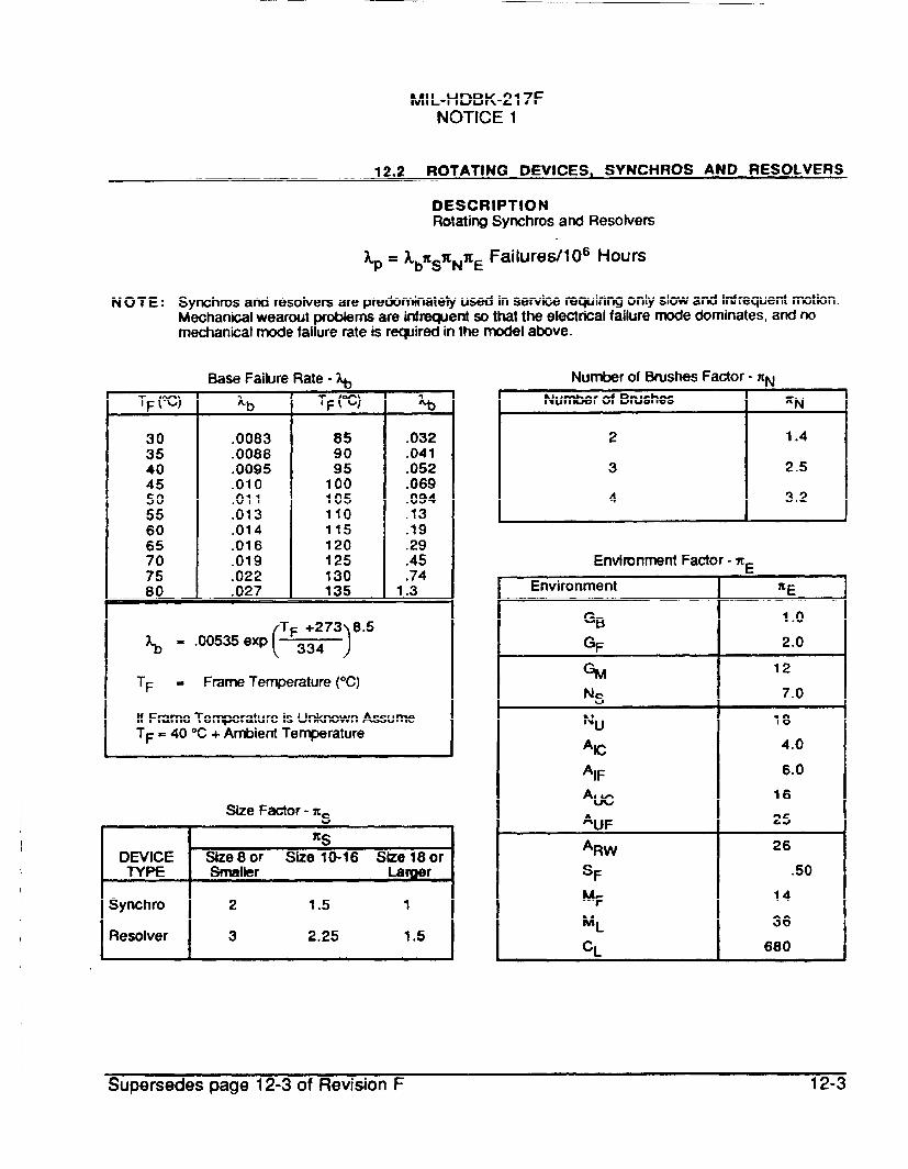
12.2 ROTATING DEVICES, SYNCt-fROS AND RESOLVERS
DESCRIPTIONRotating Synchros and Resolvers
kp = kbfi~x~z~ Failures/l OGHours
N O TE: Synchros and resolvers are predominately used in service requiring only slow and infrequent motion.M-echanical wearout problems are Infrequent so that the electkal failure mode dominates, and nomechan”kal mode failure rate is required in the model above.
i3ase Failure Rate - ~
TF (Z) k~ TF (%) h
30 .0083 85 .03235 .0088 90 .04140 .0095 95 .05245 .010 100 .06950 .011 105 .09455 .013 110 .1360 .014 115 .1965 .016 120 .2970 .019 125 .4575 .022 130 .7480 .027 135 1.3
%= .00535 exp
C’J:’3)8”5
TF = Frame Temperature (“C)
If Frame Te~rature is Unknown AssumeTF = 40 ‘C + Ambient Temperature
Size Factor - ZS
%s
DEVICE Size 8 or Size 10-16 Size 18 orTYPE Smaller LaWr
Synchro 2 1.5 1
Resolver 3 2.25 1.5
Number of Brushes Factor-XNNumber of Brushes 1 %N
2 1.4
3 2.5
4 3.2
Environment Factor - n.
Environment
GB
GF
%
Ns
Nu
AC
‘IF
‘UF
‘RW
SF
MF
E
ltE
1.0
2.0
12
7.0
18
4.0
6.0
16
25
26
.50
14
36
680
Supersedes page 12-3 of Revision F 12-3

MIL-HDBK-217F
._.
12.3 ROTATING DEVICES, ELAPSED TIME METERS
DESCRIPTION
Base Faik.we Rate - k
-.– —--- —mapsea
x Failures/l Oe l-tours‘P = ‘b% E
Type IAb
A.C.
Inverter Driven
Commutator D.C.
20
30
80
Temperature Stress Factor - ~T
-rating T (“C)/Rated T (%) I XT
o to .5 .5
.6 .6
.0 .8
1.0 1.0
Environment Factor - Xr*
Environment nE
%3 1.0
+ 2.0
GM 12
his 7.0
Nu 18
AC 5.0
‘IF 8.0
Am 16
‘UF 25
‘RW 26
SF .
MF 14
ML 38
CL N/A
.50
12-4
M1l--HDBK-2l 7F
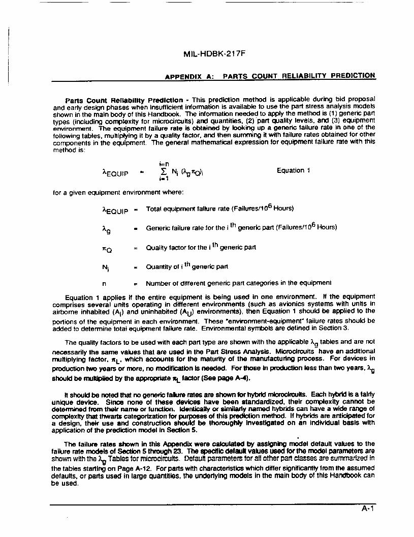
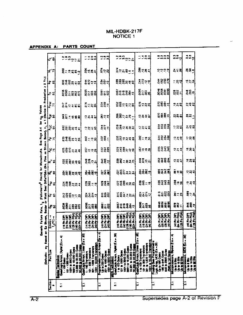
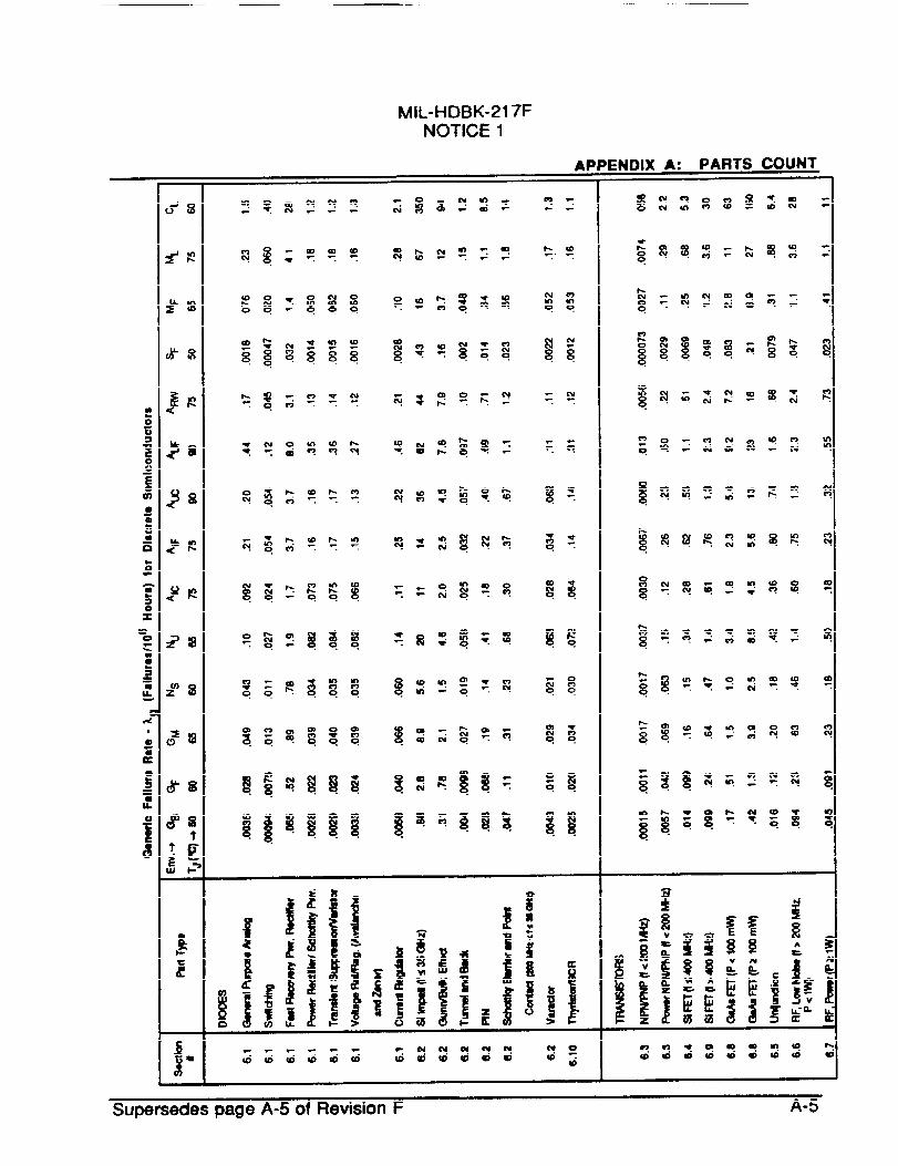
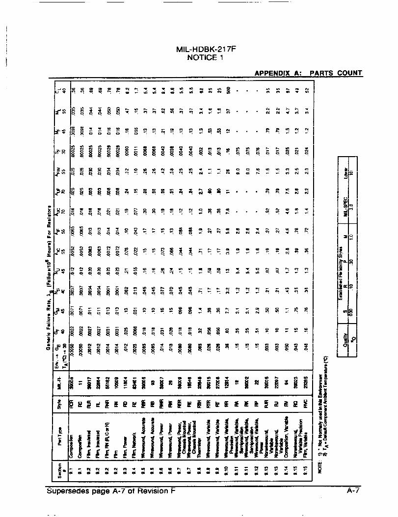
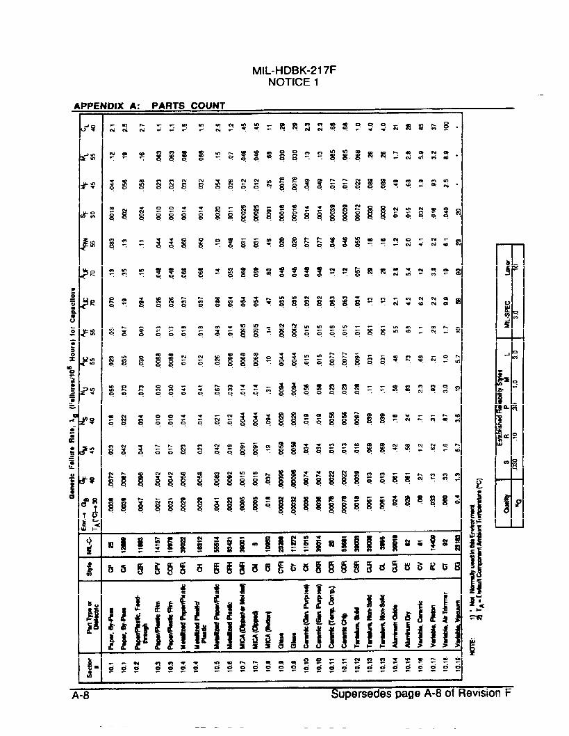
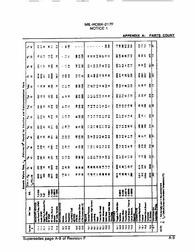
APPENDIX A: PARTS COUNT RELIABILITY PREDICTION
Parts Count Reliability PredictIon - This prediction method is applicable during bid proposaland early desgn phases when insufficient Informatbn is avaiiable to use the parl stress anaiysis modelsshown in the main body of this Handbook. The informat~n needed to appiy the method is (1)generic parttypes (inciuding complexity for micmcircuk) and quantities, (2) “part quality Ieveis, and (3) equipmentenvironment. The equipment failure rate is obtained by looking up a generio failure rate in one of thefoiiowing tables, multiplying it by a quali factor, and then summing it with failure rates obtained for othercomponents in the equipment. The general mathematical expression for equipment failure rate with thismethod is:
i= n
‘EQUiP = Z ‘i (~~i Equation 1i= 1
for a given equipment environment where:
Total equipment fafiure rate (Failures/106 Hours)
Generic faiiure rate for the i ‘h generic part (Faiiure#l 06 Hours)
Quaiity factor for the i ‘h generic part
“thQuantity of I generic part
Number of different generic part categories in the equipment
Equation 1 appiies if the entire equipment is being used in one environment. If the equipmentcomprises severai units operating in different environments (such as avionics systems with units inairborne inhabited (Ai) and uninhabited (Au) environments), tmn Equat@n 1 shou~ ~ aPPiied to the
portions of the equipment in each environment. These “environment-equipment” faiiure rates should beadded to determine totai equipment failure rate. Environmental symbols are defined in Section 3.
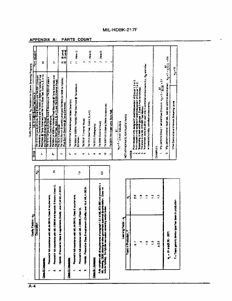
The quality factors to be used with each part type are shown with the applicable Ag tabies and are not
necessarily the same values that are used in the Part Stress Analysis. Microcircuits have an additionalmultiplying faotor, %L, which aooounts fOr the ~tUfitY Of the ~n@aduffn9 Pmce~. For dev~s in
production tw years or more, no rnodifioatbn fs needed. For those in pmductfon less than two years,%
should be nnJlt@lied by the appmpdate ~ factor (See page A4).
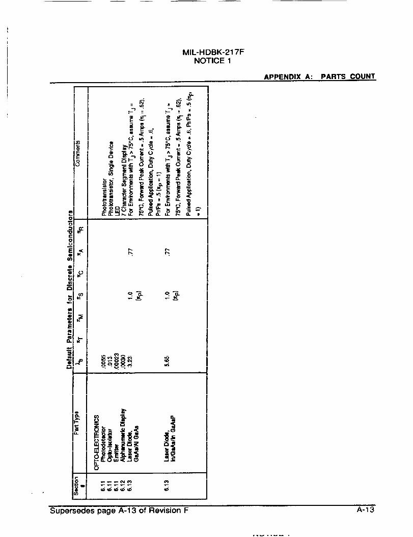
It should be noted that m gene~ failure rates are shown for hybrfd rnbrodrcults. Eachhybrfdk a talrtyunique devke. Shoe none of these devices have been standardized, their complexity canmt bedetermined from their name or function. identically or similarly named hybrids can have a wide range ofcomplexity that thwarts categorization for pwposes of this prediction method. If hybrkfs are anticipated fora design, their use and instruction should be thoroughly Investigated on an individual basis withapplication of the prediction model in Section 5.
The failure rates shown in this ~ndlx were oabuiated by assigning rnckel default values to thefailure rate models of Seotbn 5 through 23. The speolfio defwk vake6 used for the model parameters areShOWflwith the ~ Tables for tiU’OCiKMitS. Default pararl10tef6 for all other part classes are sununarized in
the tabies starting on Page A-12. For parts with characteristics which differ signif”~ntiy from the assumeddefautts, or parts used in large quantities, the underlying models in the main body of this Handbook canbe used.
I I la. ❑ ldKILl
A-1
LJ I
MIL-HDBK-217FNOTICE 1
APPENDIX A: PARTS COUNT
,
. . .u+ IUi I4 IUi I
A-2 Supersedes page A-2 of F3evision F

MIL-HDBK-217FNOTICE 1
APPENDIX A: PARTS COUNT
.mwo
..-ed. . . .
hmhutm co-ooo-0000.
-tomr-Qmu000-.
mu)al*tnln 80.000
I I I
Nai*loom000. . .
Inf-cw Q0-.000
!3W?g. . .
,
II m
1
Supersedes page A-3 of f3evision F A-3
=., . --—- —- -v -. *w p”*.””
MIL-HDBK-217F
APPENDIX A: PARTS COUNT —
mId8
+Cu
t?
m
?
0
.
A-4
d’s
MIL-HDBK-217FNOTICE 1
AP
r-Cu @!&f0-0
E !!II>
ENDIX A: PARTS COUNT
!?
Supersedes page A-5 of Revision F A-5

MIL-HDBK-217FNOTICE 1
APPENDIX A: PARTS COUNT
A-6 Supersedes page A-6 of Revision F
MIL-HDBK-217FNOTICE 1
APPEhlDIX A: PARTS COUNT.
?%persedes page A-7 of Revision F A-7
MIL-HDBK-217FNOTICE 1
DIX A: PARTS COUNT
0 0*“
0
mi
0
*
0
Ui
i-0
t,
w00.
CN
$
G8
A-0 Supersedes page A-80f Revision F
MIL-HDBK-217FNOTICE 1
APPENDIX A: PARTS COUNT
Ii9
Supersedes page A-90f Revision F A-9

MIL-HDBK-217F
APPENDIX A: PARTS COUNT
to
*
m
8
Ui
!30
*A
(u
Ui
mei
ml
m
*
.
UI
0“
1
I
— ,I
A-10

MIL-HDBK-217F
APPENDIX A: PARTS COUNT
r-Oi
0.
0u)
0ti
0w
0O.i
0.
0Oi
0.
0Ln
0.
0Y
00 0-. .
F
egii
.
A-n

MIL-HDBK-217FNOTICE I
—
Ann~UIniV A . Da D-e nnI IIIT
w
A-12 Supersedes page A-12 of Revision F
I
I
MIL-HDBK-217FNOTICE 1
APPENDIX A: PARTS COUNT
A
+7
u
1!IL
34
i%
Supersedes page A-13 of Revision F A-13
-—-- —..—

MIL-HDBK-217FNOTICE 1
APPENDIX A: PARTS COUNT
A-14 Supersedes page A-1 4 of Revision F

MIL-HDBK-217F
APPENDIX A: PARTS COUNT
Itr
I{nlllluullu Ullunllltau nun -Za
I f?:
m
I I
A-15
— — — — — —

MIL-HDBK-217FNOTICE 1
APPENDIX A: PARTS COUNT
m
%
ii
q-
0
+
OcoInw
HzK+
H
1!x
i! LLaa
A-16 Supersedes page A-16 of Revision F
!1 ,, l.–. 1
Related Documents