MIL-HDBK-217F BEF?1991 SUPERSEDING MIL-HDBK-217E, NotIce 1 2 J8nwry 1990 MILITARY HANDBOOK . RELIABILITY PREDICTION OF ELECTRONIC EQUIPMENT AMSC N/A DISTRIBUTION STATEMENT A: Approved for public release; distribution unlimited. Downloaded from http://www.everyspec.com

MIL-HDBK-217F Reliability Prediction for Electronic Equipment
Oct 24, 2015
Reliability Prediction for Electronic Equipment
Welcome message from author
This document is posted to help you gain knowledge. Please leave a comment to let me know what you think about it! Share it to your friends and learn new things together.
Transcript
MIL-HDBK-217FBEF?1991
SUPERSEDINGMIL-HDBK-217E, NotIce 12 J8nwry 1990
MILITARY HANDBOOK.
RELIABILITY PREDICTION OFELECTRONIC EQUIPMENT
AMSC N/A
DISTRIBUTION STATEMENT A: Approved for public release; distribution unlimited.
Downloaded from http://www.everyspec.com
MIL-HDBK-217F
DEPARTMENT OF DEFENSEWASHINGTON DC 20301
RELIABILllY PREDICTION OF ELECTRONIC EQUIPMENT
1. This standardization handbook was developed by the Department of Deferwwith the assistance of the military dep~ments, federal agencies, and industry.
2. Every effort has been made to reflect the latest information on reliabilityprediction procedures. It is the intent to review this handbook periodically toensure its completeness and currency.
3. Beneficial comments (recommendations, additions, deletions) and any pertinentdata which may be of use in improving this dooument should be addressed to:Commander, Rome Laboratory, AFSC, AlTN: ERSS, Griffiss Ak Force Base,New York 13441-5700, by using the self-addressed Standardization DocumentImprovement Proposal (DD Form 1426) appearing at the end of this documentor by letter.
....—
Downloaded from http://www.everyspec.com
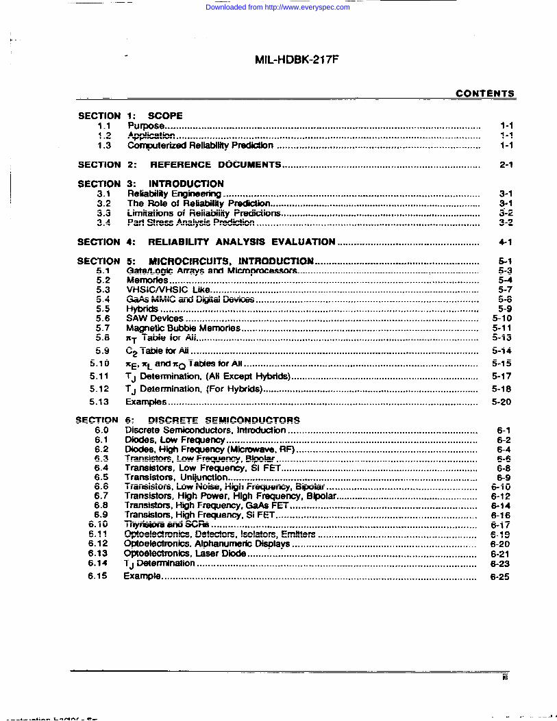
I. MIL-I+DBK-217F
CONTENTS
SECTION1.11.21.3
SECTION
SECTION3.13.23.33.4
SEHION
SECTION5.15.25.35.45.55.65.75.85.9
5.105.115.125.13
SECTION6.06.16.26.36.46.56.66.76.86.9
6.106.116.126.136.146.15
1: SCOPEPurpose .... .. .... ..... .. .. ... ... ....0...... .... .... .... ● . .... ....... ........ .. .● ...... . .. .. .... .... ... ..... .. ... .... ....Application .. ...... ...... .... ...*.. ......... .... .... ...... . ● ,, *........ ..........*. .....*...... .... ........ ..... .. ......@rnputefized RdiabWty Predktbn .. .... .. .... ...... .. ....... .. .... .. .. .... .. .. ...... ... .. .... ..... ... .....
2: REFERENCE DOCUMENTS ● ... ... ....... .... .. ................... .. .. ... ... ... .... ... .... ... .....
3: INTRODUCTIONReliability Engineering . ........ .. . . . . . . . . . . . . . . . . . . ...0 . . . . . . . . . . . . . . . . . . . . . . . . . . . . . . . . . . . . . . . . . . . . . . . . . . . . . . . . . . .
The Role of Reliability Predktbn ...**.*.*..... ......... ................ ......... ................. .............Limitations of Reliability Predictions ● ..... *..*.*... . . . . . . . . . . . . . . . . . . . . . . . . . . . . . . ● . . . . . . . . . . . . . . . . . . . . . . . . . . . .
Part Stress Analysis Prediction ..... ........ ........ ...... . .. .... .. ● ..... ...... ... ... . ...0.. .... ... ... .... ....0
4: RELIABILIN ANALYSIS EVALUATION .................. ...*..*... ... ............. .......
5: MICROCIRCUJTS, INTRODUCTION .......**...**.....................0..... ● .................C3ate/Lo@cArrays and Microprocessors ...... ..................................*... .....*..... .............Memorfes ... ..... .... .... .... .... ...... .. . ...... .... .. .. .... ........ ...... ... .......... .... .. .... .... .. ..... .. .. ........VHSICNHSIC Like ... ........ ....... ........... ... ...... ........ .... ....... ....... .... .................... ..........GaAs MMIC and D@ai Devioes . ........ .... .............. ... ...... ........ ..... ... ..... .. .... .. .... .. .. .......Hybrids . .. .. ............ .... ...... .... ... ...... .. ........ ........ .... ....... .......... .... ...... ........ ... .. .. ... ... ....SAW Devices .... .......... .. .... .... .. ...... ... .... .... .....● . ... .... ...... ... .... .. ...... .... .. .. ... ...... ..........Magnetic Bubble Memories ........ ............ .... .. ... .... .......... .... ...... ... .. ... ..... .. ...... .. .. .. .....XT Table for All .......... ............ ...... ...... ............ ...... ................... ........ ...... ............ .......C2 Table for AIl . ....... .... .... ........ .... ....... .. ...... .. .... .............. ... .. .... ... ..... .. .......... ...........%EsXL and fiQ Tabk= for ~i ..... ........ .... .... .... ... .. .. ........ ...... ... ....... ....... ........ .. .. ...... ...TJ Determination, (All Except Hybrids) ...................................*... ............* ..................TJ Determination, (For Hybriis) ........... ......... ........................................... .......● .........Examples .... ........ ........ .. .. ................... .. ........ .... .. .... ..... .... .......... ...... .... .... ... ...... .... ..
6: DISCRETE SEMICONDUCTORSDiscrete Semiconductors, Introduction ....... ........... ....... ......... .... .. ... ..... .. ... .... ... ..... ...Diodes, Low F~ency ..... ........ .... .. .......... . .. .. ........ ...... ....... . . . . . . . . . . . . . . . . . . . . . . . . . . . . . . . . . . .
Dbdes, High Frequency (Microwave, RF) .... .......... .... .. ........ ..... ........ .... ....... .. ..... ......Transistors, LOW Frequency, Bifx)lar ... .... .... ....... ... .... ..... .... ...... .... .. .... ..... ........ ... ... ...Transistor, Low Frequency, Si FET ..... ............... ............................................... ...*..Transistors, Unijmction ..........00....................... .............. ....... ........ .......... ........... ... ...Transistors, Low Noise, High Frequency, Bipolar . ..... ..... .... ...... ... ... ... .... .. ..... .. .. ........ .Transistors, High Power, High Frequency, Bipolar .....................* ..........* .............. ... ...Transistors, High Frequency, GaAs FET .. .. ..... .............0.... .. .... .... ... ... .... ....... .. ...........Transistors, Hgh Frequency, Si FET ....... ....* ... .. ..... ... ... ...... .... ...... .. .... . .... ...... .... .... ...~ end SCRS .... .... ........ ........ .... .. ........... .... ...... ........ . ● ... .. .... .. .... .. .... ...... .. . ....Optoelectronics, Detectors, Isolators, Emitters ........ ........ .. ... .. .......... .. .... .... ... .. .... .....Optoeiectmnios, Alphanumeric Displays ... .... .. .... ................. .. .... ...... .... ... .... ... ..... .. ...OploekWonios, Laser Diode ................. ......* ...... .. ............ .... .... ... ...... .. ..*...... . .... ... ..TJ Determination ..... .. .... .... .... ............ ... .... .... ...... .. ...... .. .... ..... .... ...... .... .... ..... .. .... ....Example . ..... .... .. ........ ... .... ......... ............... .... ...... .. .................... .. .... ....... .. .... .. .........
1“11-11-1
2“1
3-13-13-23-2
4-1
5-15-35-45-75-85-9
5-105-115-135-145-155-175-185-20
6-16-26-46-66-86-9
6-106-126-146-166-176-196-206-216-236-25
...HI
Downloaded from http://www.everyspec.com
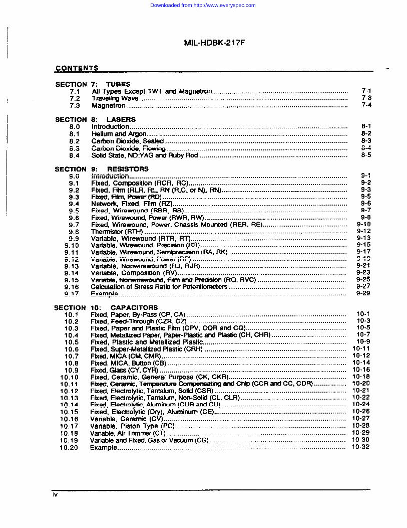
MIL-HDBK-217F
CONTENTS —
SECTION7.17.27.3
SECTION8.08.18.28.38.4
SECTION9.09.19.29.39.49.59.69.79.89.9
9.109.119.129.139.149.159.169.17
SECTION10.110.210.310.410.510.610.710.810.9
10.1010.1110.1210.1310.1410.1510.1610.1710.1810.1910.20
7: TUBESAll Types Except TM/T and Magnetron ........ ....................................................... ....... 7-1Traveli~ Wave . ....... .... ...... .... ........... ...... .. ...... .. ........ .... ......... .............. .. ...... ........... 7-3Magnetron .. .. .......... .... .... .. ........ ... .......... .. .... ...*..... ...... .......... .. .... .......... ..... .........0.. 7-4
0: LASERSIntroduction ... .................... ..... .... .. .... ...... .. ...... .... ......... .......... .. .. ............. .... ...... .. .... 8-1Helium and Argon . .......... ... .......... .... ..... .... ... ..... .. ...........** . ... .... .... .... .... ...............* . .. 8-2Catin Dmxide, Sealed . .... .. ............ .. ....... ... ... .... ...... .. ...... .. .. ... ........ ...... .. ...... ....... .. 8-3Carbon Dioxide, Fbwing .... .. ...... .... ........ .... ... .... .. .... ...... .... ....... ........ ...... ........ ......... 8-4SoIii State, ND:YAG and Ruby Rod .... .... .... .... ... ............ .. ............ .. .. .. ..... .... ...... .... ... 8-5
9: RESISTORSIntroduction .... ... ... ....... ............ ... .. ........ .... ... ... ................... .. .. ........ .... ......... ...... .. .. .. 9-1Fixed, Composition (RCR, RC) ................................. ............................... ................. 9-2I%@, Fitm (RLR, RL, RN (R.C, or N). RN) . ............................ . ....... .... .................... .... 9-3Fixed, Fltrn, Power (fWI) ........ ........ ...... ........ ... .. .. .......... .. ................... ............ ........... 9-5Network, Fixed, Film (RZ) .. ........... ............. ............. .............. .................... ................ 9-6Fixed, Wirewound (RBR, RB) ... ......... ................... ............................ .................. ...... 9-7Fixed, Wkewound, Power (RWR, RW) ......... ...... .... .. .... ... .......... .. ........ .. ........... ...... ... 9-8Fixed, Wirewound, Power, Chassis Mounted (RER, RE) ............................................ 9-1oThermistor (RTH) .......... ..... ........ .... ..... .... ...... .. .. .... .... ..... .... .... ........ .. ............ ... .. .. .... 9-12Variable, Wirewound (RTR, RT) ......... ................................................................. ...... 9“13Variable, Wkewound, Precision (RR) ......... ....... ... ....... .......... .... .... ..... ................. ...... 9-15Variable, W/rewound, Semiprecision (RA, RK) . .... ................ ....... ................... ..... ..... . 9-17Variable, Wkewound, Power (RP) . .......... .. ...... .. .. ..... .......... .... .... ....... .... ........ ..... ...... 9-19Variable, Nonwirewund (RJ, RJR) ................................ ........................................... 9-21Variable, Composttlon (RV) ...................*.. ........ ................................ ...... .. ................ 9-23Variabte, NOnwmwu nd, Fitmw’KI Prectsion (RQ, RVC) ... .... ........ ....... .. .... ................ 9-25Cakulation of Stress Rat& for Potent&meters . .... ........ .... .... ..... .... .... .. .. .... ..... ........ ... 9-27Example . .. ..... .. ...... ....... ...... .... ..... ...... .... ... .. .. ............. .... .... ... .... .. ................... ......... 9-29
10: CAPACITORSFixed, Paper, By-Pass (CP, CA) .. .... .... ...... ...... .. .. ... .... .... .......... ....... .............. ........ ... 1o-1Fixed, Feed-Through (CZR, CZ) . ........ ...... ........ .. ....... ...... .... .... ......... .. ...... .... .... .... ... 10-3Fixed, Paper and Plastic Fitrn (CPV, CQR and CQ) ..................................................... 10-5Fixed, Metallized Pqw, Paper-Plastic and Plastic (CH, CAR) .. ...... .. .... ... ............... .... . 10-7F&ed, Plastic and Metallized Plastic .............................................. ............................ 10-9Fixed, Super-Metallized Plastic (CRH) ........ ....... ..................... .... ........ ....... ...... .... ..... 10-11F&ed, MICA (CM, CMR) ........ .. .. .... .............. ... .. .. .. .. ...... ........ ............. ...... .. ...... .... ..... 10-12Fixed, MICA, Button (CB) ..... .. ....* . .... .......... .. ... .... .... .... .......... ..... .. ..... ..... .... .... .... .. ... 10-14Fued, GJass (CY, CYR) ......... ........ ............. ....... ... ...... ............ ..... .. .. .... .... .. .. .... .... ..... 10-16Fixed, Ceramic, General Purpose (CK, CKR) ............................................................. 10-18Fixed, Cerarnk, Tenpemtum ~ . and Chip (CCR and CC, CDR) . ...... ........ . 10-20Fixed, Electrolytic, Tantalum, Solid (CSR) ........ .... .... .... .... ............. .... ....... .. .. ........ .. ... 10-21Fixed, Electrolytic, Tantalum, Non-Solid (CL, CLR) ... .... .... .... ..... ........ ... ......... ..... .... ... 10-22Fbd, Ektrotytic, Aluminum (CUR and CU) .... .. ...... .... .. .... ... .... .... .. .. .. .. ..... .... ...... .... . 10-24Fixed, Electrolytic (Dfy), Aluminum (CE) ...................................... .............................. 10-26Variable, Ceramic (CV) .. .......... ............ ............. ........................ ................................ 10-27Variable, Pkton Type (PC) ........ ......... ......... ......... ......... ................... ........................ 10-28Varitie. ArTfimmr (C~ ............. ...... ........ .. ........... ...... ...... ....... ... ..... .... ........ ...... ... 10-29Variable and Rxd. Gasor V.um(CG) .. .... .. ..... ......... ... ...... ........ .... ... .... ......... ...... .. 10-30Example ... ..... ........ .. ............ ... ........... .. .. ..... .... .. ..... .... .... ........... .... ..... .... ........ ..... .. .. 10-32
iv
Downloaded from http://www.everyspec.com
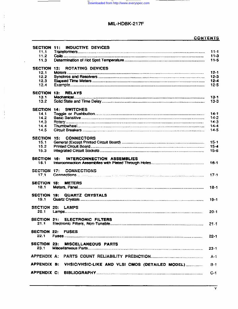
——
MIL-HDBK-217F
CONTENTS
SECTION11.111.211.3
11: INDUCTIVE DEVICESTransformers ........... .... .... .......... .. .... ..... .... .... ... ... ...... .... ....... .... .. .. .... ...... .. ..... .... .... .. 11-1
11-311-5
cob .... .....*.. ........... ..................................................................*...... .....................Determination of Hot Spot Temperature ............................... ........ .....................0...0..
SECTION12.112.212.312.4
12: ROTATING DEVICESMotors . . .... ........ .... .....* ● .. ........ .. .......... ......... .... ...... .. .. .... .............. ..... ........ .............Synchros and Resolvers .............. .... ........ ..... .. ...... .... .... ........... ... ....... .. ............ ... ....EIapsed Time Meters . .. .. .... ............*.. .. ........ .... ... ..... .... .... ............ ....... .. .. .... ........ ... ..Example ... ...... .. ... .. .. ..... ........ ......... ........... .. .... .. ..... .... ........... ...... .. .. ... .. .......... ..... ....
12-112-312412-5
II SECTION
13.113.2
13: RELAYSMechanbl ......................................0..● ..... .......... ..........● ...................................0.....SolidState and Time Delay . . . . . . . . . . . . . . . . . . . . . . . . . . . . . . . . ...*..... . . . . . . . . . . . . . . . . . . . . . . . . . . . . . . . . . . . . ..0......
13-113-3
(
I SECTION 14: SWITCHESToggle or Pushbutton ............ ..... ...... ...... ........ .... .............. .......... .. ... ... ............ ........Basic sensitive .. .... ...... .. .. .......... .. .. ... ...... .... .. .... ...... .... .... ....... ............ ........ .. .. ... .... ..Rotary .. ... .......... ...... ... .... ...... .. .......... .... ...... ... ...... .. .... ........ .... .... .. ..... ....... ... .... .... ...Thumbwheel ... .. ....... ....... ...... ....... .... ........ .... ........ .. .... ........... ...... ...... ....... ... ..... .... ..Circuit Breakers . ........ ........ .... .... ...... ........... .... .. ... ....... .... ....... .... .. .. .... .... ........ ..... ....
14.134.214.314.414.5
14-114-214-314-414-5
SECTION15.115.215.3
15: CONNECTORSGeneral (Except Printed Cir@t Board) .......... .... .... ...... ... .. ...... .... ... ..... ... .... .... .... .......Printed Circuit Board . ... ........ .... .... ...... .... ... .... .... .. .. .. .. ........... ...... .. ...... ...... .. .. ....... ....Integrated CituJlt Sockets .. ...... .......... ...... .. ... .......... .... .... .. ...... ... .. .. .............. .... .... ...
15-115-415-6
SECTION16.1
16: lNTERCONNECTtON ASSEMBLIESlntemomectkm Assenb+ies with Ptated Through t-totes . .. ....... ....... ... .... .... ........ ....... . 16-1
SECTION17.1
17: CONNECTIONSConnections ....................................................................... ................................... 17-1
SECTION18.1
18: METERSMeters, Panel .... ...... .. .... .. .. ................... .... ...... .... ...... .... ... .... ........ ........ .... .... ... .... .... 18-1
SECTION19.1
19: QUARTZ CRYSTALSQuartz Crystals....................................... .............. .................................................. 19-1
SECTION20.1
20: LAMPShmp .. ... .. .. .... ...... .... . ...... ...... .... ........ .. .... .. ....... ... ... .... .... .... .... .. .. . .. .... ........ .. .. ....... 20-1
SECTION21.1
21: ELECTRONIC FILTERSEiectmrtb Fitters, NorwTunabte................................................................................ 21-1
SECTION22.1
22: FUSESFuses . . . ....0.... ● .. .. ....... ........ .... .......... .... ............ ... .. .... .. .. .... .... ....... .. ..... ... .. .. .. ......... 22-1
SECTION23.1
23: MISCELLANEOUS PARTSMiscellaneous Patis ....... ..... ......... .. .... ... .... .... .... .......... ....... .... ........ .. .... ........ .. ....... .. 23-1
APPENDIX A: PARTS COUNT RELIABILITY PREDICTION ....... .... .. ..... . ..... . .. .. .. .. ... ... .. . A-1
APPENDIX B: VHSIC/VtiSIC-LIKE AND VLSI CMOS (DETAILED MODEL) ... .. .. ... ... . B-1
APPENDIX C: BIBLIOGRAPHY .......... .... .......... .... ... ...... .... .... .. .... ....... ...... ........ ............ ... .. c-1
v
Downloaded from http://www.everyspec.com
MIL-HDBK-217F
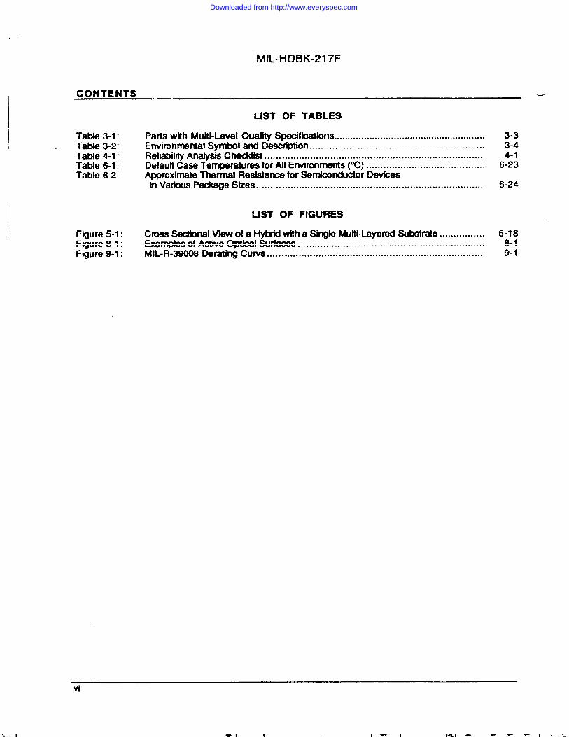
CONTENTS —
LIST OF TABLES
Table 3-1:Table 3-2:Table 4-1:Table &l:Table S2:
Figure 5-1:Figure 8-1:Figure 9-1:
Parts with Multi-Level Quality Spedfications .............................. ..........................Environmental Symbol and Desdptiin ..............................................................Reliability Analysis Cbckfist ...... ............... ... .. .......... .... ........ ..... ........ .. .......... ....Default Case Temperatures for All Environments (~) ..... .. .... ....... ................. .......Approximate Thermal Resistance for SernbncWtor Devicesin Various Package Sizes ..... .... ..... ............. .... ........ .... ........ ... ............ .... ...... ... .
LIST OF FIGURES
Cross Sectbnal Vk!w of a Hybrid with a Single Multi-Layered Substmte ......... ... .. ..Examples of Active O@cal Surfaces ....... ........ ...... ... .... .... ... ..... .. ............. .... .... ...MIL-R-39008 Deratinfj cum ... .. ............. ........................... ... ................. ... .. ... .. .
3-33-4.
6:2;
6-24
5-188-19-1
vi
Downloaded from http://www.everyspec.com
MIL-HDBK-217F
FOREWORD
This revision to MIL-HDBK-217 provides the following changes based upon recently completed studies(see Ref. 30 and 32 listed in Appendix C):
1. New failure rate prediction models are prov-kled for the following nine major classes ofmicrocircuits:
● MonoliihE B~lar Dqital and Linear Gate/lm@c Array Devioes
● Monolithic MOS Digital and Lmar Gate/Logic Amy Devfces
● Monolithic B@olar and MOS Digital Microprocessor Devkes (Including Controllers)
● Monolithic Blpotar and MOS Memory Devices
● Monolithk (W@ Di@tal Devices
● Monolithic GaAs MMIC Devices
● Hybrid Microcircuits
● Magnetic Bubble Memories
● Surface Acoustic Wave Devices
This revision provides new prediction models for bipolar and MOS microcircuits with gate counts up to
60,000, linear microcircuits with up to 3000 transistors, bipolar and MOS digital microprocessor and co-
processor up to 32 bits, memory devices with up to 1 nlftion bits, GaAs monolithic microwave integrated
circuits (MMICS) with up to 1,000 active elements, and GaAs digital ICS with up to 10,000 transistors. TheCl factors have been extensively revised to reflect new technology devices with improved reliability,andthe activation energies representing the temperature sensitivity of the dice (nT) have been changed for
MOS devices and for memories. The C2 factor remains unchanged fmm the previous Handbook version,
but includes pin grfd arrays and surface mount packages using the same model as hermetic, solder-sealeddual in-line packages. New values have been included for the quality factor (~), the learning factor (~),
and the environmental factor (@. The rrwfel for hybrid microcircuits has been revised to be simpler to
use, to delete the terrperature dependence of the seal and interconnect failure rate contributions, and to
provide a method of oakulating ohp jundon temperatures.
2. A new model for Very High Speed Integrated Circuits (V1-fSIC/VHSIC Like) and Very LargeScale Integration (VLSI) devices (gate counts above 60,000).
3. The reformatting of the entire handbook to make Heasier to use.
4. A reduction in the number of environmental fado~ (~E) from 27 to 14.
5. A revised failure rate model for Network Resistors.
6. Revised models for Ms and Ktystrons based on data supplied by the Electronic IndustriesAssociation Microwave Tube DiWon.
vii
-- . ...=-------- - —---- --u. I -- 1 -u I
Downloaded from http://www.everyspec.com
MIL-HDBK-217F
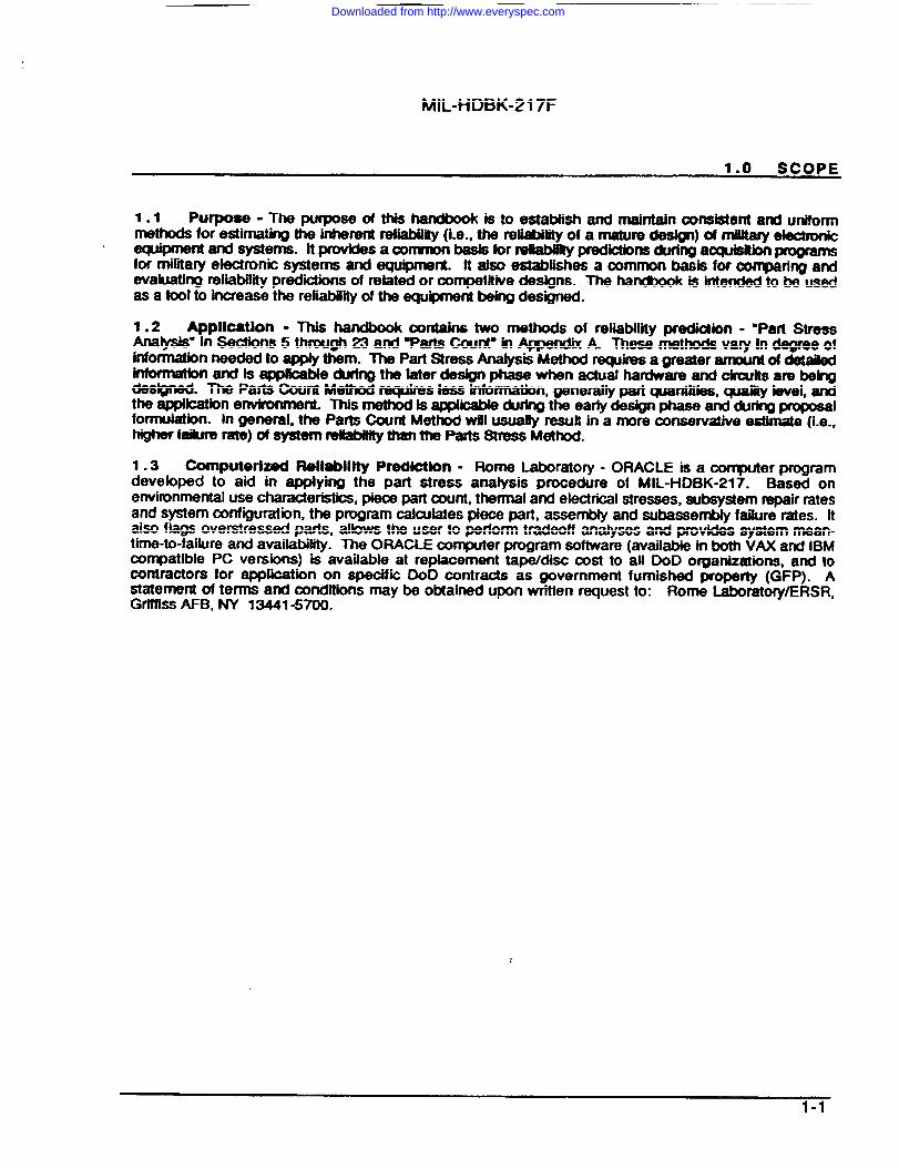
1.0 SCOPE
Purpoee - The purpose of thfs MruboOk is to establish and maintain consistent and uniformti.~ for estimating the hhemnt rek&Slity (i.e., the reUabflityof a mature design) of rnilbry @edron&~~~ - systems. It provides a common basfs for ~ predictionsckhg aoquis&bnprogmmsfor military ebctrcmc systems and equipment. h atso establishes a common basis for oomparfng andevafuatlng reliability predictions of rdated or competitive destgns. The handbook is intended to be usedas a tool to increase the reliabil”~of the equ@merxbeing designed.
1.2 Appllcatlon - This handtmok oontains two methods of reMWiJitypmdiotbn - “Part StressAnalysis” In Sectfons 5 through 23 amf 7%rts Count- in Appendix IL These methods vary in degree ofinformatbn needed to apply them. lhe Part Stress Anafysii Method recpires a greater amount of detailedIn&mtfon and ts appfkabfe mrfng the later design phase when actual hardware and c&wits are beingdesigned. The Parts Count Method raquires less infonnatbn, generally part quantities, qmtity level, andthe applkatbn environmen& This method Is appfioable cMng the early de- @ase and du~ pmpo@formulation. In general, the Parts Count Metfwd wffl usually result in a more conservative estknate (i.e.,~f*mte)ofsy’stem r@taMtythanthe Parts Stress Method.
1.3 Computerfzad Rellablllty PmcffctlOn - Rome Laborato~ - ORACLE is a computer programdeveloped to aid in appfying the part stress analysis procedure of MIL-HDBK-217. Based onenvironmental use chamcteristks, piece part oount, thermal and electrical stresses, subsystem repair ratesand system configuration, the program calculates piece part, assemMy and subassembly failure rates. Italso flags overstressed parts, afbws the user to perform tradeoff analyses and provides system mean-time-to-failure and availability. The ORACLE computer program software (available in both VAX and IBMco~atible PC versbns) is available at replacement tape/disc cost to all DoD organizations, and tocontractors for applbcatbn on spedfk DoD contraots as government furnished property (GFP). Astatement of terms and conditions may be obtained upon written request to: Rome Laborato~/ERSR,Grtffiss AFB, NY 13441-5700.
f-l
I 1 I
Downloaded from http://www.everyspec.com
..-”, .-
,..-,
. .
MIL-tiDBK-217F
2.0 REFE!?ENCE DOCUMENTS
~s~cites somespecificatbns which have beencanoslle dofwhiohdescrb ectevicesthatamnottobeused fornewdes@n. lWiinfomatti&s Wms$arytmcxamesomeofthesed evicasarusecfinsoalfed %ff-th~ eqdpment which the Depwtment of Defense purchases. The documents citedmthis section are for @dance and information.
SPECIFICATION
MIL-C-5
MIL%l 1
MlL-R-l 9
MIL-G20
MIL-R-22
MIL-C-25
MIL-R-26
MIL-T-27
ML-(X2
MIL-G81
MIL-92
MIL-R-93
MIL-R-94
MIL-V-9S
W-L-111
W=
W-F-1726
w-f-i814
MfL-G3098
MIL-G3807
MIL-G3643
MlL4N8so
SECTION #
10.7
9.1
9.11
10.11
9.12
10.1
9.6
11.1
10.15
10.16
10.18
9.5
9.14
23.1
20.1
14.5
22.1
22.1
19.1
15.1
15.1
15.1
Ca@&s, FMed,Mii-Dieisctric, General Specifii for
~, F&a composition (Insufated) General $pecuii for
Resiekx. Variab&gWirewound (Low Operating Tmpwatum) GeneralSpo&@atbn for
@Pw@%=d~ “~ v@fw=- ~)Estdfkhed and Nonestabiished Reliability, General Specifiiion for
Rask!or, Wuewow Power Type, General Spa&cation for
~. fiti p~r~~~ Dire Cwrent (HermeticallySealedin Metal Case@, General Specification for
Resistor, Fued, Wkewound (Power Type), Genarai Specifhbn for
Tmnsfonner and fndwtor (Audio, Power, High Power, High PowerPulse). General Sfxdiibn for
~r. Fiu~ ~fo~~ (DG fgruminum.W E~@,Pdar&ed), Gened spadkamn
Capacitor, Variable, Ceramic Dielectric (Trimmer). General Specificationfor
Ctpcitor, Variable, Air Dielectric (Trimmer), General Specificaii for
Resistor, Fwed, Wkewound (Aocura!e), General Spdfkdon for
Resistor, Variable, Composition,General Specifiin for
Vior, Interrupter and Self -RectifyingO General Specification for
-. hadaant Miniature, Tungaran Fikment
Ckauit Br@der, MOidOdC&m, BrarmflcfrcuRand~
Fuse, Q@ridge, CJassH (Thii mvem renewable and mrwnebie)
Fuse, Camidge, High InterruptingCqmcity
_ Unk ~ ~~end Spcifiw&m for
Connector,Coax&~Radii Frequency, Series Pulse, Gene@,SpdMlOns for
Connector, Coaxial, Radio Frequency, Series NH, Associated Ftiings,~neral s~ for
Connector, Coaxial, Radio Frequency, Series LC
I Luw u I
Downloaded from http://www.everyspec.com
MIL-HDBK-217F
2.0 REFERENCE DOCUMENTS.
SPECFKATJON
Mt4X655.
ML-C-3767
MIL-S-3786
MfL-G3950
MIL-G3965
MIL+5015
MIL-F-5372
MIL-R-5757
MIL-R-6106
MIL-L-6363
MIL-S-8805
MIL-S-8834
MlL-M-l 0304
MlL-R-l 0509
MIL-C-1095O
MIL-C-1101S
M!L-GI 1272
MlL-C-l 1693
MlL-R-l 1804
MIL-G12889
MIL-R-12934
SECTION #
15.1
15.1
14.3
14.1
10.13
15.1
22.1
13.1
13.1
20.1
14.1, 14.2
14.1
18.1
9.2
10.8
10.10
10.9
10.2
9.3
10.1
9.10
conneotor, P&q and Ramptda, _(Jl=SeriasTwin)andAssociated Fitlmgs, General SpuM@mn.
~. f’q ~ ~ (po”~* B&~ TYP@ -~~SpacMiion for
S*. Rotary (Circxit Selector, Low-Current (Capady)), General~bn for
=. Toggle, Envlmnmantally sealed, General Speckatbn for
=b~~~ Elti~ (No-lkf Electrolyte), Tantalum, General
~, Eledrkal, Circular Threaded, AN Type, GeneralSpedflcation for
I%aa, Currati Limiter Type, Amaft
Relay. Electrbl (For Electronic and Communkation Type Equipment),General Specifbaticm for
Relay, Electromagnetic (Including Established Reliability(ER) Typs),~-~s~ for
bnp, Incandemt, Aviation Service, General Raquiramentfor
SwhcheSand Switch Assemblies, Swxdtivo and Push, (SW Action)General Sfx@in for
Switches, Toggle, Positive Brealq General Specification for
Meter, Electkal Indicating, Panel Type, Ruggedzed, GeneralSpedficatbn for
Resistor, f%cad IWm (High Stability). General Speoikatbn for
-Or, Fud, Mii Dielectric, Button Style, General Specifiiionfor
~, FU~, Ceramic Dtiric (General Pupae), Ganeral~bn for
Capadtor, Fixed, Glass Dlelectrb, General Spcfkatbn for -
Capadtor, Feed Through. Radio Interference Reduction AC andDC,
l!!’!!’. Sdedh Metal Casos)Eatabkhed and No~ “ hed
MaMfiio General Spdicatbn for
Resistor, Freed, Film (Power Type), General Specifiin for
“Cap&or, By-Pa&: Radio - Interfermce Reduction, Paper Dielectdc,AC d DC, (Hermetbally Sealed in Metallk Casas), GaneralSpectficatbn for
Resistor, Variable, Wirewound, Preasion, General Specification for
2-2
r- . . . –n / nv -1 [1-/!1, --- --– .uu l-- ,-- -------- —. n . ——. ba -
Downloaded from http://www.everyspec.com
MIL-HDBK-217F
2.0 REFERENCE DOCUMENTS
sPEcfFlcATloN
ML-C-141S7
MIL-G14409
MIL-F-15160
MK-C-IS305
MfL-F-15733
UL-GW312
ML-F-13327
MIL-R-16546
MIN-19500
MIL-R-19523
ML-R-19M8
ML-C-19978
MIL-T-21036
MUA-21097
MIL-FM2097
MIL-R-Z?664
MIL-S-2271O
ML-S-22665
MIL-C-22W2
ML+163
M&GZ3269
MIL-FW3265
SECTKMJ #
10s
10.17
22.1
11.2
21.1
10.4
21.1
9.7
6.0
13.1
13.1
10.3
11.1
15.2
9.13
9.2
14.4
14.1
1s.1
10.19
10.9
9.1s
~, -d: a (pap- PI-tic) or mastic Dweot* Directcurrent (Hermabd lySeabdin Matal Cases) amMshed Refkwty,@J-~ ~n for~. v- (Pii TyP, T“lar Trimmer), GWWraISpac#ioatbn for
Fuse, Instmnem Poww amf Telephone
Coil, Fixed and Vari*, Radio Frequency, General Specifiibn for
FBtler,Rack Imarkmrux, General SpecMin for
~. -, Metzdl&ed (Paper, Paper Plastic or Plastic Film)Dbbdrk, Dkocl Cummt (Herrneticaliy sealed in Metal Cases), Gemral~ibn for
Filter, High Pass, k Pass, Band Pass, Band Suppression and DualFuncknkg, General Specdfiition for
Redstor, Freed,WWewound(Power Type, Chassis Mounted), GeneralSpecificatbn for
SomkOnductor Oevice, Geneml Specification for
Relay, Contmi, Naval Ship&oard
Roley, Tree, Delay, lherm~ General Specifiition for
~or, Fmecf Plastic (or Paper-Plastic) Dielectric (HermeticallySealed m Metal, Cemmc or Glass Cases), EstafXished andNoneatabiiahed ReGabilii, General Specifiicatbn for
Transformer, Pulse, Low Power, General Specikatiin for
Connector, Electrical, Printed WInng Board, General Purpose, GeneralSpedfbatbn for
Rasistor, VarMMe, Nonwirewound (AdjustmentTypes), GeneralSpedfbatbn for
Resistor, F&d, Film, lnsdated, General Specifiiion for
S*. Mary (Printed Circuit), (Tlwmbwheel. In-1ine and Pushbutton),-nerd ~*
Switches, Pushbutton, Illuminated, General Specification for
Connector, Cyfinddcal, Heavy Outy, General Specification for
= ~~ ofi,v*. V=xum MI-* General Specifiibn
em. Fi~. G- Diekrik Estiiiihed Reliabllky, GeneralSpeclkatbn for
Reaiir, Variable, Nonwirewound, General Specificationfor
2-3
. .
Downloaded from http://www.everyspec.com
MIL-HDBK-217F
2.0 REFERENCE DOCUMENTS
SPECfFICATlON
MIL-F-23419
MIL-T-23648
MfL-G24308
MIL-G25516
MfL&+6482
MN-R-27208
MIL-C-2f1748
MIL-R-28750
MfL-G288tM
MIL-C-2884O
MIL-hR851 O
MIL-H-38S34
MIL-I-38535
MIL-C-38999
MfL-C-39001
MIL-R-39002
MfL—G39003
MIL-R~
MtL+39006
MfL-Raoo7
sEcTKm #
22.1
9.8
15.1
15.1
15.1
9.9
15.1
13.2
15.1
15.1
5.0
5.0
5.0
15.1
10.7
9.11
10.12
9.5
10.13
9.6
Fuse, bstrumont Type,Gonad ~km for
Thormistw, (Tharmafly Sensitive Resistor), Insulated, GenerafSpadfioatbn for
Connec40r, E- Rectangular, Miniature Polatizad Shell, Rack andPanel. Genoraf Spodcatbn for
Cortnector, ~ , Miniature, ~ Environment Resistant Type.-~~fof
Cormoctor, Efoctr&f (Circular. Minirdure, QuH kamnoc&Environment Rl&ting) ReU@ac& and Plugs, General Spocik@ionfor
Resistor, VariaM, WKewound, (Lead Screw Actiied) GeneralSpeciftiion for
Con-or, Ebct~ Rectangular, Ra& and Panel, solder Type andCrimp Type Contads, General Spacifiition for
Relay, Solid State, Ganeral Specification for
Connector. E&ctric Rectangular, High Density, PoMzed CantralJa&euww, Genoraf Spedficstion for, Inactive for New Designs
Conrmdor, ~ cimUlar Threaded, High Denaity, High ShockShipboard, Class D, General Spechation for
M&oc5rcuits, Generaf Specificatii for
Hybrid Microcircuits, General Specification for
Integrated Circuits (Microcircuits) Manufacturing, GeneralSpeclfiiion for
Qxvwc#or, E~ Chcular, Miniature, Hgh Density, QuickDisconnect, (Bayonet, Threadad, and Breech Coupiing) EnvironmentResistant Remowble Crimp and Hermetic Solder Cmtacts, GeneralSpecifiiion for
qor. ~~, Mh Dkktk Estabkhed ReliaMfity, GeneratSpecification for
Raa&stor, Variable, Wkewound, Sem&Precision, General Spa&icstionfor
-’ ‘a_~&*ewg T-lJm*●
Raslatcx, Fixed, ~nd, (Aaamte) EstaMshed Fteflabllity, GeneralSpecification for ‘
-N. ~~. -I& (NortsoMf Ek%rolyte) TantalumEstalMshed Relilii, General SpadkMon for
Resistor, Fixed, W~ nd (Power Type) EstaMished Reliability.General Speckition for - “- -
.
Downloaded from http://www.everyspec.com
.-. . . . . . . . .
MIL-HDBK-217F
2.0 REFERENCE DOCUMENTS
SPEOFICATR3N
MIL-R~
MLC-3901O
MIL-CX9012
UL-C39014
MK-C49015
MIL-R39016
MtL-R-39017
MIL-G39018
MIL-C-39019
MIL-G39022
MIL-R-39023
MIL-R-39035
MiL-G49142
MIL-P-5511O
MIL-R-65W2
MIL-G55235
MIL-G55302
MIL—G65339
MIL-G65514
MIL-C-5S629
MIL-T-S5631
SECTION #
9.1
9.7
11.2
15.1
10.10
9.9
13.1
9.2
10.14
14.5
10.4
9.15
9.13
15.1
152
9.2
15.1
15.2
15.1
10.5
14.5
11.1
Redstor, Fixed, Campoah“ n, (Insutated) Established Reliability,Genefal S@fio@hfor
R@!sMcw,m ~nd (Power Type, chassis Mounted) ~EstaMished R@aMfity, General SpecMcMion for
Cd, Fbrti Radio Frequency, Molded. Established Ratiiity, GeneralSpec#iibn for
Connector, Coaxial, Racfb Frequency, General Spdfii”~ for
~. ~ Carandc Dielectric (General purpose) EsMMbhdR8iiabili!y,Gmeral SpeoWation for
Rdetor, V*, WkewOund (Lead screw Actuated) EmabfishedReliability,General Spdfkatbn for
Relay, Electromagnetic, Established ReIiabilii, General Specifiitionfor
Resietor, Freed, Fh (insulated), Estabkhed Reliabitky,GeneralSpecifiikm for
Capacitor. f%ed, Ebctmlytio (Aluminum Oxide) Established Reliabil.~and Nonestablished ReKaMIity, General SpecdfbNion for
Cfrcutt Breakera, Magn@iq Low Power, Sealed, Trip%ee, General~bn for
~r, ~d. Mettiized Paper, Paper-Plastic Film, or Plastic FilmDielectric, Direct and Alternating Current (Hermetically Sealed m MetalCaaas) Estabfbhed Reliability, General Specification for
Resistor, Varkble, Nonwirewound, Precision, General Specification for
Resistor, Variable,Nonwhwound, (Adjustment Type) EstablishedReliability, General Spedkttbn for
Conne@or,Triaxial, RF, General Specification for
PrintedWdng Boards
Resbtor,F~~EstddWd Reliabilii, General Specification for
Connector. Coaxial, RF, General Specif”=tion for
Connector, Printed Circuit, Subassembly and Accessories
Adapter, CoaJC~ RF, General SpeMc8tbn for
qor. ~~, ,~k (CWM@tdfizd Plastic) Dielectric, DirectCurrent In Non-Metal Cases, General Spedfii”bn for
Circuit Breaker, Magnetic, Unsealed, Trip-Free, General Specificationfor
Transformer, Intormdiato Ftewemx, Radio Frequency, andDiscriminator, General Specific&lon”for . -
Downloaded from http://www.everyspec.com
MIL-HDBK-2 17F
2.0 REFERENCE DOCUMENTS
SPECIFICATION
ML-C-55681
MlL~1511
MIL-(X3383
MtL-R-S3401
MiL-G83421
MIL-C-83513
ML-C-83723
MIL-R=72s
MIL-R-63726
MILoS-83nl
MN-C-83733
MIL-S43734
STANDARD
SECTION#
10.11
15.1
14.5
9.4
10.6
15.1
15.1
13.1
13.1, 13.2,13.3
14.1
15.1
15.3
~r, Chip.M@t@lebayer, Freed,Ceramic Diekct~ EstablishedRewility, General Sp&iGat”m for
Conne, Ekc&icaf, Circular, High Demity, Quiok Dmnect,EnvhonmentResisting, and Acc=swies, General SpecHMh for
Circ@i6reaker, Remote ~ntrol, Thermaf, TripFree. GeneralSpecMiion for
Resbtor Notwodq Fixu!, Fti. Ganwal Spdkabn for
~r, f%cf Supennetallizodf%stb f% DiskcMc(DC, ACor DCand AC) Hmwtb#y Soalecf in Metal Cases, ~bhed Refiabiiity,ud~~
Cwmecbr, EkcZrical,Rectangular, Mbrominiaturo, Polarized Shell.Garbefal Specification for
Connedor, Ebctricd (Circular Environment Resisting), Receptaclesand Plugs, GeneraJ Speclficatbn for
Relay, Vacuum, GoneraI Specification for
Relay, lime Delay, Elec!ric and Electronic, General Specifiiion for
Switch, Toggle, Unsealed and SealedToggle, Ganeral Specifiin for
Conmw%x, Ebc!dc@, Miniature, Rectangular Type, Rack to Panel,EnvironmentResisting,200 Degraas C TcxalContinuousOpOfa@JTemperature, General Spedcatbn for
socket Pl@n Electronic Components, General Specifiikm for
MIL-STD-756 Rehbility Modeling and Prec&tbn
MIL-STD-883 Test Mathods and Prmxdures for Microelectronics
Mk4TD-975 NASA Star#ad E&trid. Efactronicand EbctmmachanbalPartsLkt
MIL=WD-1!547 Pmt8, Matwials ●nd Procasses fof Spaco Launch Veh&k8, TechnioaIRequirements for
MtL-Sl’D-1~ ~ Requtrwnents?orHyMd Mcrockufl FacflltWJand Unes
c o pies of specImat&ns and Stmdads required by contractors in comectbn with spcific acquisitionfunctbns should be oMlnad fmrn the contractingactivityor as directed by the a)ntracting offiir. ~ngle_ - ako available(withoutcharu8)uponwrfttenrequest to:I
StandwdizatbnDocumentOrderDesk700 Robins Ave.Building 4, Seotion DPhiladelphia,PA 19111-5094(216) 697-2867
------ ----- —-W
2-6
— ~_––“. v., . . ~“.-y..,-..-- “,. - . . -----
Downloaded from http://www.everyspec.com
/MIL-HDBK-217F
I 3.0 INTRODUCTIONI
I
3.1 Rellablllty Englneerlng - Reliability k currently recognized as an essential need in miIitaryebctronic systems. It is looked upon as a means for -cing costs fmm the factory, where rework ofdebotive cxmpcments adds a mn-proddve overhead expense, to the field, where repak costs Inotudenot onty pa~ and labor but also transportation and storage. More knportantly, reliabilitydirectly inpactsforce effectiveness, measured In terms of availability or sortie rates, and determines the stze of the“bgisticsw inhibitingforce utilization.
Th e achievement of reliability is the fumtbn of refiabifity engineering. Every aspect of an eleotrodcsystem, from the purtty of matertals used in fts oomponent devices to the operatots Inteflaoe, has animpact on reliability. RelMWty engineering must, therefore, be appbd throughout the system’sdevelopment in a dillgent and timely fashion, and integmted wfthother engbewhg disoi@nes.
A variety of reliability engineedng tools have been developed. This handbook provides the modelssupportinga basic tool, reliabilitypredctbn.
3.2 The Role of Reflablllty Prediction - Reliability predictbn provides the quantitative baselineneeded to assess progress in reliabWty engineering. A prediction made of a proposed design may beused inseveralways.
A characteristic of Computer Aided Design is the ability to rapidly generate alternative solutions to aparticular problem. Reliability pmdiibns for each design alternative provide one measure of relative worthwhich, mrWned with other considerations, will aid in selecting the best of the available options.
Once a design is selected, the reliabilii predktii nwiybe used as a @de to Iwpmvement by showingthe hphest contdbutorsto faifure. If the pwt stressanalysis method is used, it may also rewaf otherWtfulareas for change (e.g., over stressed parts).
The Impact of proposed design changes on reliabilityoan be detemnktedonly by comparfng the reliatMtypredictionsof the existing and proposed designs.
The abllttyof the design to maintain an accepable reliability level under environmental extremes may beassessed through reHaMty pmdictbns. The predctkms may be used to evafuate the need forerwtronmentalcontrol systems.
The effects of complexity on the probability of mission success can be evaluated through reliabilitypredictions. The need for redundant or baok-up systems may be determined with the aid of reliabilitypredictions. A tradeoff of redundancy against other reliability enhancing techniques (e.g.: more oooling,higher part quality, etc.) must be based on reliability predictions coupled wfth other pertinentconsiderations such as cost, spaoe limitations, eto.
The predbtbn will also he~ evahwte the s@fficance of reportscf fallume. For exa@e, if emmml falkrresof one type or oo~nent occur In a system the predkted faliure rate can be used to determine whetherthe number of failures Is commensurate with the number of components used in the system, or, that itindicates a pmbbm area.
Finally, reliability predictbns are useful to varbus other engineering analyses. As examples, the locationof txdtt-h-test circuitry 6houfd be influenced by the predicted failure rates of the chwltry monftored, andmalntenanoe strategy plannem can make use of the relative pmbabifhy of a failure’s location, based onpredictions, to minimize downtime. Reliability predbtbrts are also used to evaluate the probabilities offajlure events described in a failuremodes, effeotsand criticalityanalysis(FMECAS).
3-1
—---- -—e -- * —e–-m—~+ ... ... . .. ____.=---- - — — .———__
Downloaded from http://www.everyspec.com
MIL-HDBK-217F
3.0 INTRODUCTION
3.3 Limitations of Rellabiltty Prodktions - This handbook provides a common basis forreliability predictbns, based on anatysis of the best available data at the the of Issue. It Is interded tomake reliabilitypredictionas good a tool as possble. However, like any tool, reliabilii predktbn rrust beused htefiigently,withdue oonskferat)onof itsMnWions.
The first limitation is that the failure rate models are point estimates which are based on available data.Hence, they are valii for the condltbns under which the datawas obtained, and for the devkes oovered.Some extrapolation during model development is possible, but the inherently empirical nature of themodels can be severely restrictive. For exanple, none of the models m this handbook predict nuclearsuMvability or the effects of bnizing radiatbri.
Even when used in similar environmetis, the differences between system appliiions can be significant.Pmdkted and aohleved rWaMlty have atways been doaer for ground electronic systems than for avbnksystems, because the environmental stresses vary fess from system to system on the ground and hencethe field cor@tbns are In general cbser to the environment under which the data was oo#e@edfor theprediction model. However, failure rates are also impacted by operational scenartos, operatorcharacteristics, maintenance -s, measummmt ~es and dtlfe~~s In deftnftbn of falfure.Hence, a rellablflty predktlon should never be assumed to represent the expected field reliability asmeasured by the user (i.e., Mean-The-Between-Maintenance, Mean-Tirne-Between-Removak, etc.).This does not negate its value as a reliability engineering tool; note that none of the applicationsdiscussed above requires the predicted reliability to match the field measurement.
Electronic technology is noted for its dynamk nature. New types of devices and new processes areoontjnually introduced,compounding the difficultiesof predkting reliability. Evolutbnary changes may behandled by extmpolatbn fromthe existingmodels; revolutionarychanges may defy analysis.
Another Ilrnitatbn of retiablltty predktbns is the mechanks of the process. The part stress analysismethod re@res a signlfkant afmmt of design detail. mk naturalty knposes a time and cost permtty.More signiiioantly,many of the detatts are not avaitab+ein the earty des~ stages. For thts reason rn!shandbook contains both the part stress anatysts method (Sectbns 5 through23) and a simplerpartscountmethod (Appendix A) which oan be used in early design and bid formulatbn stages.
Finally, a basic limitation of reliability prediction is its dependence on correct application by the user.Those who correctly apply the models and use the information in a conscientious reliability program willfind the predktbn a useful tool. Those who V&Wthe prediction only as a number whkh must exceed aspecifiedvalue can usualtyfind a way to achievetheir ~at withoutany i- on the system.
3.4 Part Stress Analysls Predlctlon
3.4.1 Appltcabllfty - Th&smethod is applicable when most of the design is completed and a detailedpads list incbding part stresses Is available. ft can also be used during later design phases for rel&bilitytrade-offs vs. patl selection and stresses. Sections 5 through 23 contain failure rate models for a broadvariety d parts used in ekmtrmb equipment. The parts we grouped by major categories and, whereappropriate, are subgroupedwithin oategorfes. For mechanical and electromechanical pats not coveredby this Handbook, refer to Bibfbgraphy ftems 20 and 36 (Appendix C).
The failure rates presented appty to equipment under normal operatingconditbns, Le., with power on andperformingIts intended functbns in Its ~ended environment. Extrapolationof any of the base faihn ratemodels beyond the tabulated vahJessuch as highor subzero temperature, electrical stress values above1.0, or extrapolation of any associated model modifiers is oompletety invalid. Base failure rates can beinterpolated between electrical stress values from O to 1 using the underlying equations.
The general procedure for determining a board level (or system level) failure rate is to sum individuallycalculated failure rates for each oomponent. This summation is then added to a failure rate for the citcuitboard (which includes the effects of solderfng parts to tt) using Section 16, Interconnection Assemblies.
3-2
Downloaded from http://www.everyspec.com
MIL-HDBK-217F
3.0 INTRODUCTION
For parts or wires soldered together (e.g., a jumper wire between two parts), the connections modelappearing in Section 17 is used. Finaliy, the effects of connectingcircuitboards together is accounted forby adding in a faiiure rate for each connector (Section 15,Connectors). The wire between connectors isassumed to have a zem failure rate. For various sewice use profiles,duty cycles and redundandes theprocedures described in MIL-STD-756, Reliability Modeling and Prediction, should be used to determinean effective system ievel faiiure rate.
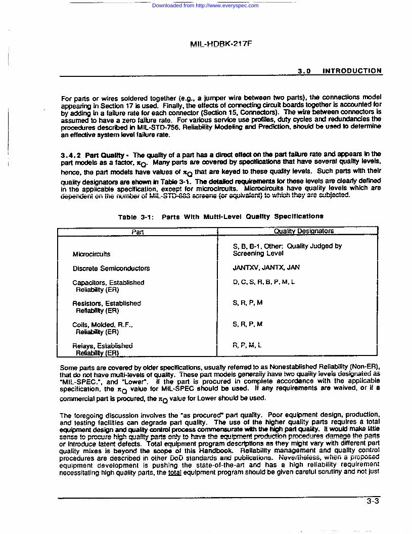
3.4.2 Part Qualtty - rne~~of apmh~am effti~ti pm fdhmratea~~mlntbpart models as a factor, *Q. Many parts am covered by spedfbations that have several quaffty levels,hence, the part models have vaiues of XQ that am keyed to these qu~~ leve~= Such Pafis w~h theirqualitydesignetora are shown h Table 3-1. The detdled requirements for these levels are ciearty defhedin the applicable specffkation, except for mkrockcuits. Mkmimfis have qualhY levels which aredepenckht on the ~mber of MIL-STD-683 screens (or equivalent) to whii they are subjected.
TatNe 3-1: Parts With Multl-Level Qua!lty Speclflcatlons
Iw was E Uvumwa 7 UWw. r.q. . . . . . -
S, B, B-1, Othec ~aliiy Judged byMicrocimuits Screening Level
Discrete Semiconductors JANTXV, JANTX, JAN
Capacitors, Established D, C, S, R, B, P, M, LReiiabiiii (ER)
Resistors, Established S, R, P, MReliablllty (ER)
Coils, Molded, R. F., S, R, P, MReiiabUty (ER)
Relays, Established R, P, M, LReliabiiily (ER)
Some Mrts are covered by older specifications, usualty referred to as Nonestablished Reliability (Non-ER),that &“ not have rnutti-levels of qu~i. These part rn&fels generally have two qualfty levels d&i@ated &‘MIL-SPEC.-, and “Lower”. If the part is procured in complete accordance with the applicablespecification, the ZQ value for MIL-SPEC should be used. If any requirements are waived, or if acommercial part is procured, the XQ value for Lower should be used.
The foregoing discussion involves the ‘as procured” part quality. Poor equipment design, production,and testing facilities can degrade pad quality. The use of the higher quality parts requires a totalW?U@M~ de$~ ~ W~ COtid processco-~rate with the high part quality. it wouid make iiilesense to procure high quality parts on!y to have the equ”qmentproductionprocedures damage the paftSor introduce latent defects. Total equipment program descriptions as they might vary with different partquality mixes is beyond the scope of this Handbook. Reliability management and quality controlprocedures are described in other DoD standards and publications. Nevertheless, when a proposedequipment development is pushing the state-of-the-art and has a high reliability requirementnecessitating high quality pans, the ~ equipment program should be given careful scrutiny and not just
3-3
Downloaded from http://www.everyspec.com
I MIL-HDBK-217FI
3.0 INTRODUCTION—
the parts quafhy. Otherwise, the bw failure rates as predicted by the models for hgh quality parts will notbe realized.
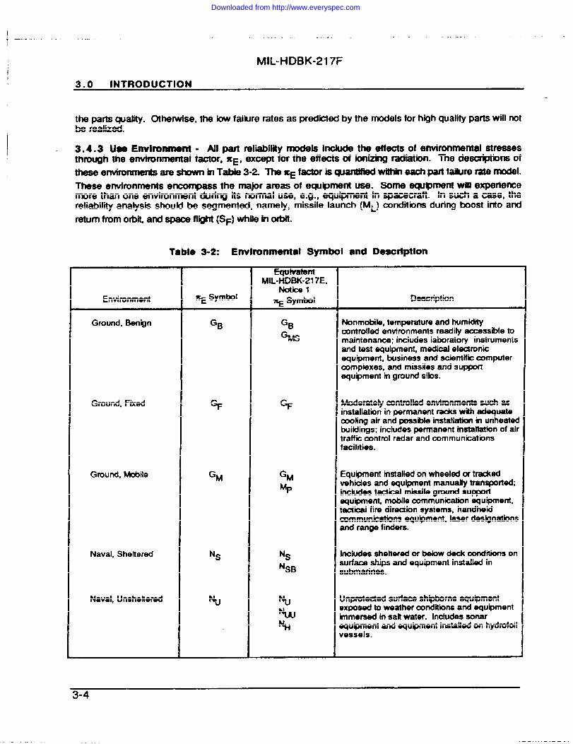
3.4.3 Uee Environment - N Dart reliabm models h@lJde the effeots of envkorlmental Streesesthrough the environmental factor,-%Er except ~orthe effects of bn~ @~~. The dem~b~ ofthese envhunentsareshownin TaMe3-2. The~fac!or isqxmtfWdwithfn eachpartfaiUre rat8rnod8l.These environments encorrpass the major areas of equprnent use. Some eqJ@ent wlfl experiencemore than one environrrwnt during its normal use, e.g., equipment in spacecraft. h such a case, thereliabitii analysis should be segmented, namely, missile launch (ML) conditions during boost into andreturnfromo~ and space flight(SF) while in orbft.
Table 3-2: Envhomnental Symbol and Deacrlptlon
EqtJhratBntMIL-HDBK-217E,
Notice 1Environment ~ Symbol ~ symbol D-ription
Ground, Bengn GB GB Nonmobile, temperature and humidity
%Scontrolled environments readily accessitde tomaintenance; includes laboratory instrumentsand test equipment, medical electronicequipment, businass and scientifc computermmplexes, and missiles and supportequipment in ground sibs.
Ground, Fixed GF % Moderately amtrolied environments such asinstallation in permanent racks with adequateoooling air and possible installation m unheatedbuildings; includes permanent tnstattatton of airtraffic control radar and communicationsfacilities.
Ground, MoMle GM GM Equipment installed on wheeled or tradwdMp vehicles and equipment manually transported;
includes ttiicai missile ground supportequipment, mobile communication equipment,tactical fire direction systems, handheld=mmunications equipment, laser designationsand range finders.
Naval, Shelterad NS NS Includes shehered or bebw deck conditions on
‘SBsurface ships and equipmant installed insubmarines.
Naval, Unsheltered Nu % Unprotected surface ahipborne equipmentNW exposed to weather conditions andequipment
immersed in salt water. Includes sonarNH $@pment and equipment installed on hydrofoil
vessels.
3-4
Downloaded from http://www.everyspec.com
I.4-..-. . . .
., ,., ,., . .. . . . . . . . . !. . . ...” ..,.. . .
. . . .., ..,..
I MIL-HDBK-217F
3.0 INTRODUCTION
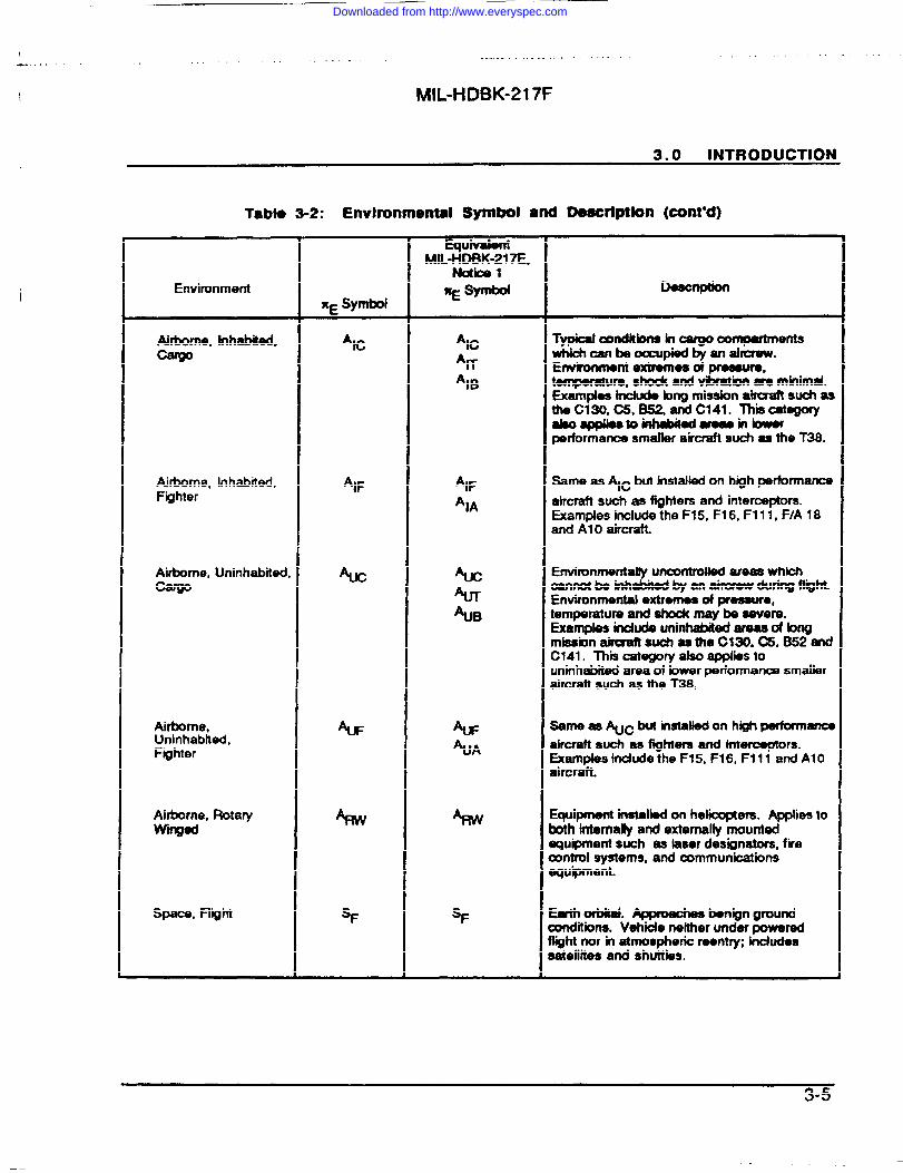
Tabto 3-2: Environmental Symbol and Deecrtptlon (CXMWd)
Environment
Airborne, Inhabitsd,
Airborne, Inhabited,Fighter
Airborne, Uninhabited,
Airborne,Uninhabited,Fighter
Airborne, Rotaryw-
Space, Flight
%E symbol
AK
‘IF
%C
AUF
ARvv
SF
E@valont
‘tcAm
*IB
‘IF‘IA
Am+%JB
%/
Description
Typical conditbns in cargo compartmentswhbhcan beoaX@adby arlahcraw.Envlronmont axhmes d ~~U~,~u~,s- and vibration W. minimal.Examplas Inctudabng missionakcraftsuchasthac130,c5, B!52andc141. Thisoatagoryaboappueata ~edaroasinbwuperformance smaller aircraft such as the T38.
Same as NC but installed on highperformanceaircraft such as fighters and interceptors.Examples include the F15, F16, F1 11, F/A 18and Al Oaircraft.
Environmentally uncontdbd areas whichoannot be rnhdited by an aircrww during flight.Environmental extrernos of pressure,tefnperature and shock maybe severe.Examples include uninhabited araas of bngmissiin ahwaft such as the C130, C5, B52 andC141. This category aiso appJiis touninhabited area of bwer performance smalleraircraft such as the T38.
Same as NC but installed on high performanemaircraft such as f~htem and interceptors.Exarnplesincludethe F15, F16, F111 and AlOaircraft.
Equipmentinstalledon helicopters. Ap@h tobothinternallyandexternallymountedsquipmentsuch as laser designators, firemntrol systems, and communicationssqu”pment.
--- APP=J— ~mw9~~~cmditions. Vehicle neither underpoweredflight nor in atmosphorio reentry; includessatellites and shuttles.
3-5
Downloaded from http://www.everyspec.com
I
I
I MIL-HDBK-217F
3.0 INTRODUCTION—
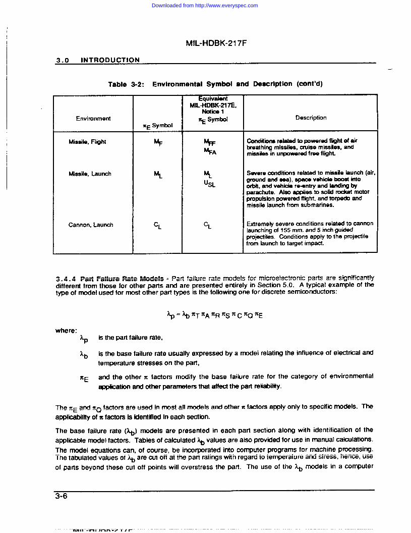
Table 3-2: Environmental Symbol and Descrfptlon (cent’d)
EquivabntMIL+fDBK-217E,
Mice 1Environment ~ Symbol Description
~E Symbol
Missile, Flight + % Conditions r.lated topoweredflightof air4A
breathing missibs, cruise missiles, andmissiles in unpowered free flight.
Miiile, Launch % \ Severe amditions relatwi to missile launch (air,u= ground and Sea), space Vshiob boost into
orbit, and vehicle re+n~ and landing bypar~e. Also applies to soI&l roclwt motorww~bn POWW@ fhght, and torpedo andmissile launch from submarines.
Cannon, Launch CL CL Extremely severe conditions related to cannonlaunching of 155 mm. and 5 inch guidedprojectiles. Conditions apply to the projectiletrom launch to target impact.
3.4.4 Part Failure Rate Models - Part failure rate models for microelectronic parts are significantlydifferent fmm those for other parts and are presented entirely in Section 5.0. A ~pical example of thetype of model used for most other part types is the folbwing one for discrete semiconductors:
~=~fiTfiA~R~S~C~Q~E
is the patt failure rate,
is the base failure rate usually expressed by a model relating the influence of electrical andtemperature stresses on the part,
and the other n factors modify the base failure rate for the category of environmentaleppkath amfother parameters that affectthe paft reKMity.
me ZE and XQfaotors are used inmost alimodels and other x factom app~ only to SWC~~ ~dels. Theapplicability of z factors is Identified in each sectbn.
The base failure rate (~) models are presented in each part section along with identification of theapplicable model factors. Tables of calculated ~ values are also provided for use in manual calculations.The model equations can, of course, be incmporated into computer programs for machine processing.The tabulated values of ~ are cut off at the part ratings with regard to temperature and stress, hence, useof parts beyond these cut off points will overstress tk pan. The use of the lb models in a ~mPuter
3-6
Downloaded from http://www.everyspec.com

MIL-HDBK-217F.
3.0 INTRODUCTION
pmgrarn should take the part rating limits into account. The ~ equations are mathematicallycontinuousbeyond the part ratings but such faiiure rate vaiues are invalii in the overstressed regions.
Aii the part modeis imiude faiiure data from both cahstmphic and permanent drift failures (e.g., a resistorpermanently falling out of rated tolerance bounds) and are based upon a constant failure rate, except formotors whch show an increasing failure rate overtime. FaiJures associated with connection of parts intocircuit asserrbiies are not imluded within the part faiiure rate models. Information on cxmnection reliabiliiis provided in Sections 16 and 17.
3.4.5 Thermal Aspects - The use of this prediction method requires the determinatbn of thetemperatures to which the parts are subjected. Sinoe parts reliability is sensftive to temperature, thethermal anatysis of any design shouid fairty accurately provide the ambient temperatures needed in usingthe part models. Of course, bwer temperatures produce better reliihty but aiso can pmc&ce hcreasedpenatties in terms of added toads on the environmental oontrol system, unless achkved throughimproved thenmal design of the equipment. The thermal analysis shouid be part of the design processand included in ail the trade-off studies covering equipment performance, reliability, weight, volume,environmental control systems, etc. References 17 and 34 listed in Appendix C may be used as guides indetermining component temperatures.
3-7
Downloaded from http://www.everyspec.com
[,,.,.... .II
,., ,. ,.. . . .
MIL
. ...! ,.- . . ..,. . . .
-HDBK-217F
4.0 RELIABILITY ANALYSIS EVALUATION
Tabie 4-1 provides a ~ . “ for evaluating a reliability predii report.For completeness, the cttecfdist includes categories for refiabiiity modeling and albcatbn, which aresometimes deiivered as part of a predctibn report. it should be noted that the scope of any reliabilityanalysis depends on the specific requirements called out in a statement-of-work (SOW) or systemspeckatbn. The inclusion of this ckkiist k not intended to change the soope of these requirements.
Tabl. 4-1: Reliablllty Anatysls CheckltetMalor COncarns Commonts—--—- -—--—-. --— m — . . . ..-
MODELSAre allfunctionalelements includedin the System designdrawingddiagrarna mustbe rwiewed toraliabiihybbdc diagram /model? be sure that the relkbilii modekfkgram qreoa with tho
hardwn.
Are all modes of operation considered in the ~ @OS, an~ae paths, degraded conditbns andnlti modd? redundant units must bedefinedandmodeted.
Do the math model results show that the design Unit failure rates and redundancy aquations are usedachieves the reliabiiii requirement? from the detailed paft predictions in the system math
model (See MIL-STD-756, Reliability Predictbn andModeiing).
ALLOCATIONAre system reliability requirements allocated Useful Ievets are defined as: equipment for(suMivided) to useful levels? sulxxmtractors, assemblies for sub-subcontractors,
arouit boards for designers.
Does the allocation process consider Conservative values are needed to prevent reallocation;am~:;?ty, design flexibility, and safety at every desgn change.
m
PREDICTIONDoes the sum of the parts equal the value of Many predictbns neglect to include all the parts producingthe module or unit? optimistic results (check for solder connections,
connectors, circuit boards).
Are environmental ccmdit”mnsand part quality Optimistic quality levels and favorable environmentalrepresentative of the requirements? cxmditions are often assumed causing optimistic resutts.
Are the circuit and part temperatures defined Temperature is the biggest driver of part failure rates;and do they represent the design? bw temperature assumptions will cause optimistic
results.
Are equ~ment, assembly, subassembly and Idontifioation is needed so that corrective actions forpart reliability drivers identified? reliabitii improvement can be considered.
Are alternate (Non MIL-HDBK-217) failure rates Use of alternate failure rates, if deemed necessary,highlighted along with the rationale for their require submission of backup data to provide credence inuse? the values.
Each component type should be sampled and failureIs the level of detail for the part failure rate rates completely reconstructed for accuracy.models sufficient to reconstruct the result?
Prediction methods for advanced technobgy parts shouldAro critical components such as VHSIC, be oarefully evaluated for imp-on the module andMonolithic Microwave Integrated Circuits system.(MMIC), Application Specific IntegratedCircuits (ASIC) or Hybrids highlighted?
II
4-1
Downloaded from http://www.everyspec.com
MIL-HDBK-217F
5.0 MICROCIRCUITS, INTRODUCTION
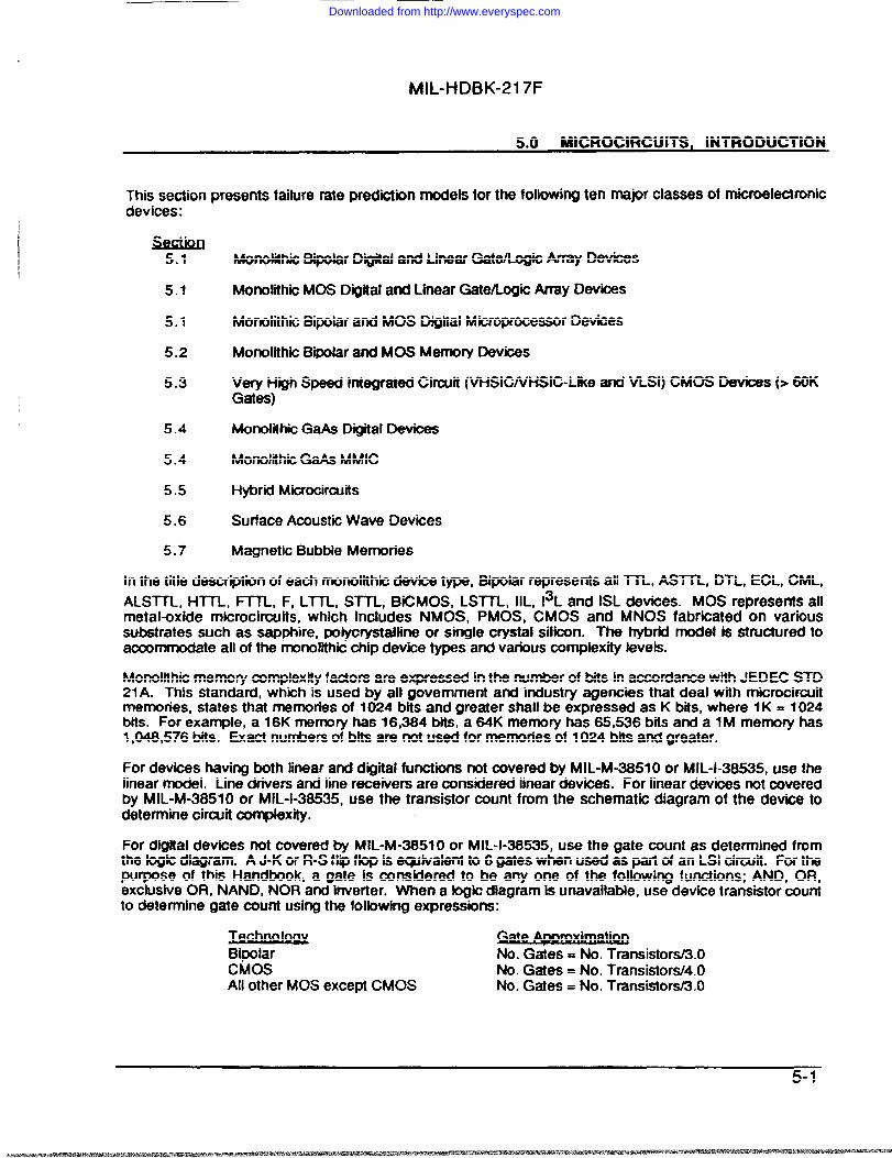
This section presents failure rate prediction models for the following ten mapr classes of microelectronicdevices:
Swis2rl5.1 Monolithic Bipolar Digital and Linear Gate/LogicArray Devices
5.1 Monolithic MOS Digital and Linear Gate/Logic Array Devices
5.1 Monolithic Bipolar and MOS Digiial Microprocessor Devices
5.2 Monolithic B~lar and MOSMemoryDevices
5.3 Very High Speed Integrated Chcuit (VHSIC/VHSIC-Like and VLSI) CMOS Devioes (> 60KGates)
5.4 Monolithic GaAs Digital Devices
5.4 Monolithic GaAs MMIC
5.5 Hybrid Microcircuits
5.6 Surface Acoustic Wave Devices
5.7 Magnetic Bubble Memories
In the title description of each monolithic device type, Bipolar represents all llL, ASITL, DTL, ECL, CML,ALSITL, HTTL, Fl_ll, F, L~L, SITL, BiCMOS, LSITL, IIL, 13L and ISL devices, MOS represents allmetal-oxide microcimuits, which includes NMOS, PMOS, CMOS and MNOS fabricated on varioussubstrates such as sapphire, poiycrystaftine or single crystai siiicon. The hybrid model is structured toaccommodate aii of the monolithic chip device types and various complex”~ Ieveis.
Monolithic memory complexity factors are expressed in the number of bits in accordance with JEDEC STD21A. This standard, which is used by ail government and industry agencies that deal with microcircuitmemories, states that memories of 1024 bits and greater shall be expressed as K bts, where 1K = 1024bits. For example, a 16K memory has 16,364 bits, a 64K memory has 65,536 bits and a 1M merno~ has1,048,576 bits. Exact nurrbers of bits are not used for memories of 1024 bits and greater.
For devices having both linear and digital functions not covered by MIL-M-3651 O or MIL4-38535, use theiinear modei. Line drivers and iine receivers are considered iinear devices. For iinear devices not coveredby MIL-M-3851 O or MiL-i-38535, use the transistor count from the schematic diagram of the devioe todetermine circuit complexity.
For digitai devices not covered by MIL-M-3851 O or MIL-I-38535, use the gate count as determined fromthe logic diagram. A J-K or R-S flip fbp is equivalent to 6 gates when used as part of an LSi circuit. For theputpose of this Handbook, a Oate is constierecf to be any one of the following functions; AND, OR,exciusive OR, NAND, NOR and inverter. When a bgic diagram is unavailable, use dev.ke transistor countto determine gate count using the folbwing expressions:
Bipolar No. Gates = No. Transistors/3.0CMOS No. Gafes = No. Transistors/4.OAl! other MOS except CMOS No. Gates = No. Transistors/3.O
5-1
Downloaded from http://www.everyspec.com
MIL-HDBK-217F
5.0 MICROCIRCUKS, INTRODUCTION
Adetailed form of the Section 5.3 VHSIC/VHSIGLikemodel is inoludedas AppendixB to allowmoredetailed WleWfs to be performed. Reference 30 should be consulted for more information about thismodel.
Reference 32 should be consulted for more Informatbn about the models appeartng in Sections 5.1,5.2,5.4,5.5. and 5.6. Reference 13 should be consulted for additional information on Section s.7.
Downloaded from http://www.everyspec.com
MIL-HDBK-217F
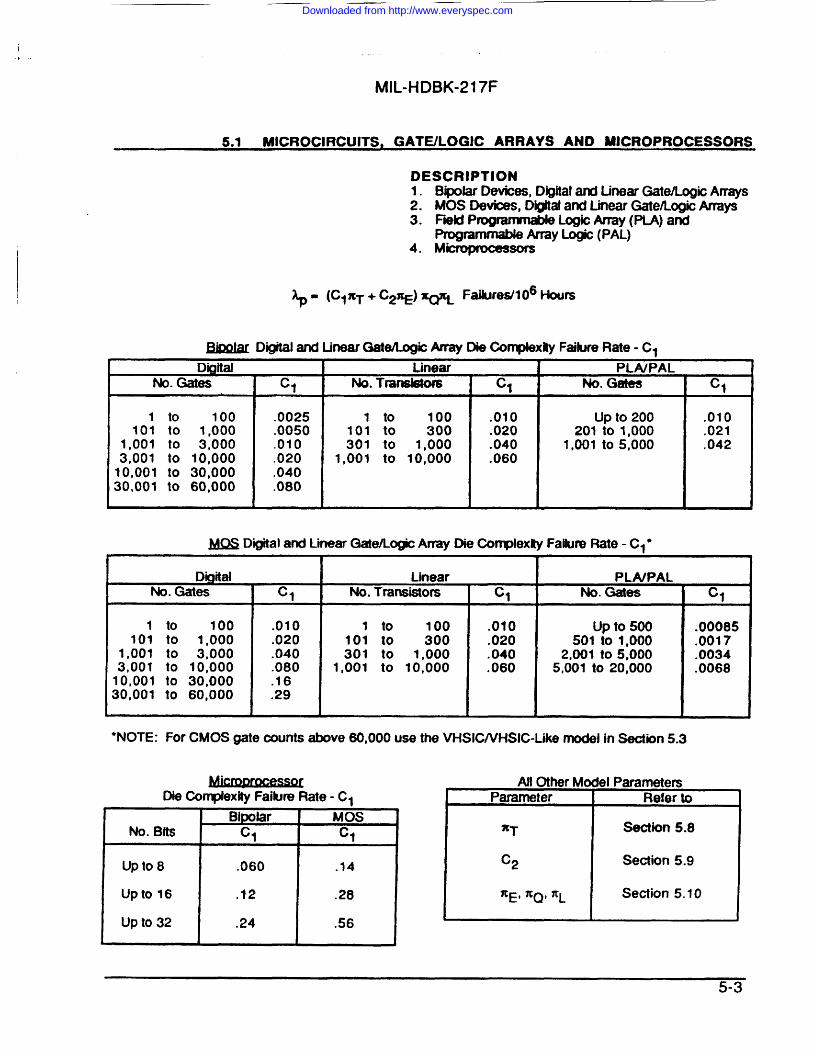
5.1 MICROCIRCUITS, GATE/LOGJC ARRAYS AND MICROPROCESSORS
DESCRIPTION1. Bipolar Devices, Digital arxf Linear Gate/Logic Arrays2. MOS Devices, Di@tal and Linear Gate/Logio Arrays3. F*H PmgranwwMe Lx ArTay (~) am
Programmable Array Logic (PAL)4. Microprwessors
~= (ClZT + C2Y@ ~ Fdlures/106 t+ours
Hgml,ar Di@al and Linear GafeA@c Amy Die Cm@exity Failure Rate-ClDighJ I Linear
No. Gates [ c. No. Transkws I c.
1 to 100101 to 1,000
1,001 to 3,0003,001 to 10,00010,001 to 30,00030,001 to 60,000
.0025
.0050
.010
.020
.040
.080
1 to 100101 to 300301 to 1,000
1,001 to 10,000
.010
.020
.040
.060
PLA/PALNo. Gates c,
up to 200 .010201 to 1,000 .021
1,001 to 5,000 .042
~ D@al and Linear Gate/Logic Army Die CorqSexlty Failure Rate - Cl”
DQitalNo. Gates
1101
1,0013,00110,00130,001
to 100to 1,000to 3,000to 10,000to 30,000to 60,000
c,
.010
.020
.040
.080
.16
.29
LinearNo. Transistors
ltol101 to 3301 to 1,0
1,001 to 10,0
c,
.010
.020
.040
.060
PLNPALNo. Gates
up to 500501 to 1,000
2,001 to 5,0005,001 to 20,000
c,
.00085
.0017
.0034
.0068
●NOTE: For CMOS gate counts above 60,000 use the V1-iSIC/VHSIC-Like model in Section 5.3
Die Complexity Failure Rate - ClAll Other Model Parameters
I Parameter Refer toBipolar MOS
No. Bits c, c,
Up to 8
II.060 .~4
Upto 16 .12 .28
up to 32 .24 .56
Section 5.8
Section 5.9
Section 5.10
5-3
Downloaded from http://www.everyspec.com
. .
MIL-HDBK-217F ..
●
5.2 MICROCIRCUITS, MEMORIES
DESCFilPTION1. Red ~ Memories (ROM)2. ~armable Read Only Memorns (PROM)3. lJ~ m- PROMS (UVEPROM)4. “Flash; MNOS and Floating Gate ElectdcaBy
Erasable PROMS (EEPROM). bOkJdf3S bothfbating gate tunnel oxide (FLOTOX) and texturedpolysiliin type EEPROMS
5. Static Rancbm Access Mermles (SRAM)6. ~ R~ /@cess Mwnories (DRAM)
~= (C1 %T + C2 %E + ~ ~ ~ FailumsH06 HOtJm
Die Complexity Faih.JmRate -Cl
Memory Size, B (Bits)
up to 16K16K<Bs64K64K<Bs256K256K<Bs1M
ROM
.00065
.0013
.0026
.0052
MPROM,uvEPROM,
z=’
.00085
.0017
.0034
.0068
>
DRAM
.0013
.0025
.0050
.010
SRAM(MOS &BiMOS)
.0078
.016
.031
.062
ROM,PROM
.0094
.019
.038
.075
lar
SRAM
.0052
.011
.021
.042
Al Factor for ~c Cablatbn ~ Factor for kc CalculationI Total No. of Programming ITotal No. of
ProgrammingCycles Over
EEPROM Life, C
up to 100100< CS2OO200< C<500500< CS1K1K<CS3K3K<CS7K7K<CS15K15K < CS20K2oK<csi30K30K < CS lOOK100K < CS200K200K<CS400K400K < C s 500K
Flotox ‘
.00070
.0014
.0034
.0068
.020
.049
.10
.14
.20
.681.32.73.4
Textured-Polp
.0097
.014
.023
.033
.061
.14
.30
.30
.30
.30
.30
.30
.30
1. Al =6.817 x10+(C)2. No underlying equation for Textured-
Poly.
Cycles Over EEPROMITextured-Poly A2
Ltfe. C
Up to 300K o
300K < C s 400K 1.1
400K < C s 500K 2.3
AJlOther McParameter
XT
C*
fiE, ~Qt XL
~c (EEPROMSonly)
IelParametemRefer to
Section 5.8
Section 5.9
Section 5.10
Page 5-5
~c = O For all other devices
5-4
. .
Downloaded from http://www.everyspec.com
I
I. .
MIL-HDBK-217F
5.2 MICROCIRCUITS, MEMORIES
w, -
All Memory Devices Except Fbtox andTextured-Poly EEPROMS
~=o
A*B*Fbtox and Textured Poty EEPROMS
~[c= 1Al 61 + ~ ‘ECC
P*Al P-54 Page 54B, Page 5-6 Page 5-6A2 A2=o Page 5-502 ~=o P* 5-6%Q Sectbn 5.10 Seotion 5.10
Error Correction Code (ECC) Optkms:1. No On-Chip ECC ~ECC = 1.0 %ECC = ~.02. On-ChP Hamming Code ~ECC = .72 %ECC = .723. Two-Needs-One ~ECC = .68 ~ECC = .66
Redundant Cell Approach
NOTES: 1. See Reference 24 for modeling off-chip error detect”on and correctionschemes at the memory system level.
2. If EEPROM type is unknown, assume Fbtox.
3. Error Correctbn Cde Optbns: Some EEPROM manufacturers have incorporatedon-chip error correction chxwitry into their EEPROM devioes. This is represented bythe on-chip hamming code entry. Other manufacturers have taken a redundant cell-~ which immporates an extra storage transistor in every memory ceil. misis represented by the two-needs-cm redndant cell entry.
4. The Al and 4 factors shown in Section 5.2 were devebped based on an assumedsystem life of 10,000 operating hours. For EEPROMS used h systems whhsignificantly bnger or shorter expected lifetimes the Al and ~ factors should bemultiplied by:
10,000
System Lifetime Operating Hours
5-5
Downloaded from http://www.everyspec.com
MIL-HDBK-217F
5.2 MICROCIRCUITS, MEMORIES
xco
x*
i
ns I
t 1
~“Fa
8m“
%6
===1 ■ I
Downloaded from http://www.everyspec.com
.—
. .. , ,,
MIL-HDBK-217F
5.3 MICROCIRCUITS, VHSICNHSIGLIKE AND VLSI CMOS
DESCRIPTIONCMOS greater than 60,000 gates
~ “ %@MFGfiPCD + ~pzEx@p~ + ~~~ Failurest106 HOUrS
Ok Base Falture Rate - ~D ANOther Model ParametersPart Type ’60
Parameter Refer toI
Logic and Custom 0.16%T Section 5.8
me Army 0.24%E~~ Se@on 5.90*
Manufaotwing Process I %FG I
QML or QPL II .55Non QML or Non QPL 2.0
Package Type CorrectionFactor - Xm‘PTI
Paokage Type Hefmetc Nm&mettc
DIP 1.0 1.3Pn Grid Amy 2.2 2.9CMp Carrier 4.7 6.1(Surface MountT@chnnlnnv\
Dle Complexity Correction Factor - ~DI Feature S&e i Die Ama (Cr#) 1
(Mkmns) As.4 .4< As.7 .7< AsI.O 1.0< As2.O 2.0< A s 3.0.80 8.0 [ 14 I 19 1 38 i 58
I 1.00 I 5.2 I 8.9 I 13 I 25 I 37 11.25 I I I I I
‘-f+) [v ‘:i+-M 58 8“2 ‘:’-’”a”sw;:bns)s)A = Total Scrbed Chip Die Area in cm2
Die Area Conversion: cm2 = MIL2 + 1S5,000
Package Base FaUure Rate - ~p Ekctrical Overstress Faiture Rate - l~h~
I Number of Pins2428404448526484120124144220
‘BP.0026.0027.0029.0030.0030.0031.0033.0036.0043.0043.0047.0060
ksp = .0022+ ((1 .72X 10-5) (NP))
NP = Nu~r of Package Pins
VTH (ESD %SC@bility (VOttS))*
o- 1000
>1000-2000
>2000-4000
>4000- 16000
> 16000
‘EOS
.065
.053
.044
.029
.0027
~OS - (-In (1 -.00057 exp(- .0002 Vw)) /.00876
‘TH = ESD Susceptibility (volts)
● Voltage ranges which will cause the pad tofail. If unknown, use O -1000 vofts.
1 UJCU7_n U Al Q! ,.,
Downloaded from http://www.everyspec.com
.-.
MIL-HDBK-217F
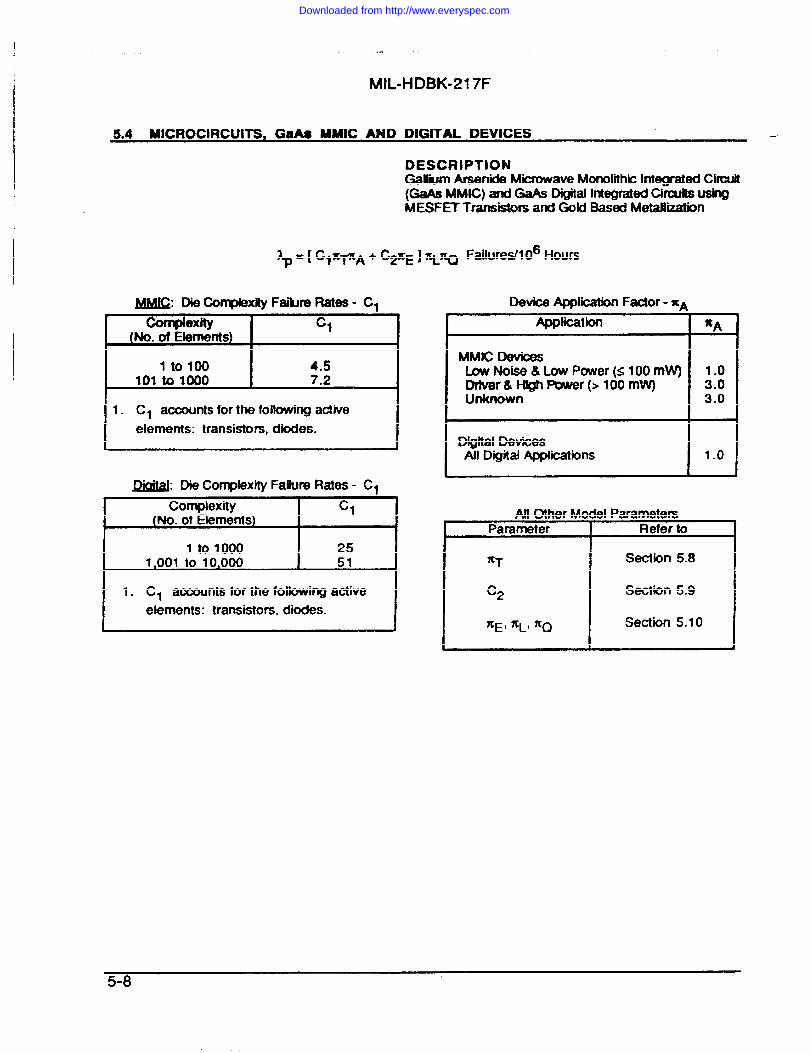
5.4 MICROCIRCUITS, GaAs MMIC AND DIG~AL DEVICES
DESCRIPTIONGa)iiim Arsenide MicrowaveMonolithic Integrated Citwit(GaIW MMIC) amt GaAs DigitaiMESF~ Transistorsand Gold
W Die Complexity FaiWe Rates - Cl
complexity c,(No.ofElements)
1 to 100 4.5101 to 1000 7.2
1. Cl accounts for the following activeelements: transistors, diodes.
-: Die CompkIXRy Failure Rates - ClComplexity c,
(No. of Elements)
1 to 1000 251,001 to 10,000 51
1. Cl aocounts tor the following aotiveelements: transistors, diodes.
hltegrated Ci-ixhsUshgBased MetaJliion
. .Application %A
MMIC DevicesLow Noise & Low Power (S 100 mVV) 1.0Drtvar& High Rnuer(> 100 mw) 3.0Unknown 3.0
Digttal DevicesAll Digital Applications 1.0
<
All Other Model ParametemParameter Refer to
XT Sectbn 5.8
C* Section 5.9
nE, XL, ~Q Section 5.10
5-8
I
Downloaded from http://www.everyspec.com
——
I? .,. .... . . .
MIL-HDBK-217F
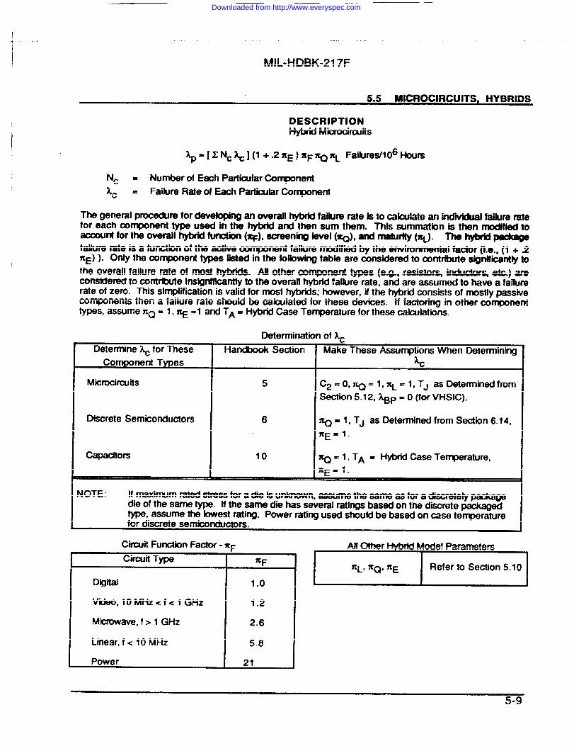
5.5 MICROCIRCUITS, HYBRIDS
DESCRIPTIONHybf@ MicrociruJits
~=[~Nc~l(l +.2XE)ICF~Iy FaMureM06Hours
Nc = Number of Each Particular Conpnentkc = Failure Rate of Each Particular Corqmnent
The general pmcechme for developing an overall hybrid faikJm rate )s to oalculde an individual failure fatefor each component type used in the hybrid and then sum them. This summatbn is then modfied toaxoun for the ovendl hybrid fumtiin (x#, suwning level (~), and matudty (~. ~ ~ ~failure rate is a function of the active mmponent faiture modified by the environmental factor (i.e., (1 + .2~E) ). Ow th ~~ne~ ~ w~ in th fob~~ t8bk ar8 rnns~~ to ~nf~e 8@Wb~& ~the overall failure rate of most hybrids. AUother cxxnponent types (e.g., m@stor& inductag et@ areconsidered to contribute lnslgnffkanttyto the overalt hybridfailure rate, and are assumed to have a failurerate of zero. This simplification is valid for most hybrids; however, if the hybrid consists of mostiy passivecomponents then a failure rate should be calculated for these devices. tf factorirm in othi?r comQonenftypes, assume ZQ = 1, ~ =1 and TA = Hybrid Case Temperature for these calculat b~s.
.
Determination of&Determine ~ for Theseco mponent Types
Microcircuits
Discrete Semiconductors
Capacitors
Handbook Section
5
6
10
Mak~ These Asswptions When DeterminingL
C2=0, XQ=l ,1= 1, TJ as Determined fromSection 5.12, ~P = O (for VHSIC).
~ = 1, TJ as Detemined from Section 6.14,%E=l.
~=1, TA = Hybrid Case Temperature,~E=l.
NOTE: If maximum rated stress for a die is unknown, assume the same as for a discretely p-die of the same type. If the same dw has several ratings based on the discrete ~type, assume the bwest rating. Power rating used sh6uld be based on case terrper~urefor discrete semiconductors.
Chcuit Function Factor -Circuit Type
Digital
Vii, 10MHz<f<l GHz
Microwave, f >1 G1-lz
Linear, f <10 MHz
Power
F
1.0
1.2
2.6
5.0
21
All Other Hybrfd Model ParametersI 1
I ~LI ~Q, ~E I Refer to Section 5.10I
5-9
I I w nfi x
Downloaded from http://www.everyspec.com
i
iMIL-HDBK-217F
I
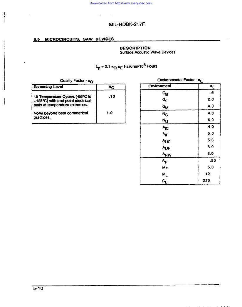
5.6 MICROCIRCUITS, SAW DEVICES
Quaiity Factor - ~
DESCRIPTIONSurfaceAcoustic Wave Devices
$ = 2.1 IQ %E Fai)ures/106 Hours
Environmental Factor - xc
Screening Level X Q
.
1 0TerTpf&mr’e Cycleal(+5% t o
I I
. 1 0+125°C) with end point electricaltests at temperature extremes.
None beyond bestcwmmwkat I 1.0practices.
L
Environment %E
%3 .5
% 2.0
% 4.0
his I 4.0
Nu 6.0
AC 4.0
‘IF 5.0
%c 5.0
‘UF 8.0
‘RW 8.0
SF .50
MF 5.0
ML 12
CL 220
5-1o
1 El I.-—
I
Downloaded from http://www.everyspec.com
MIL-HDBK-217F
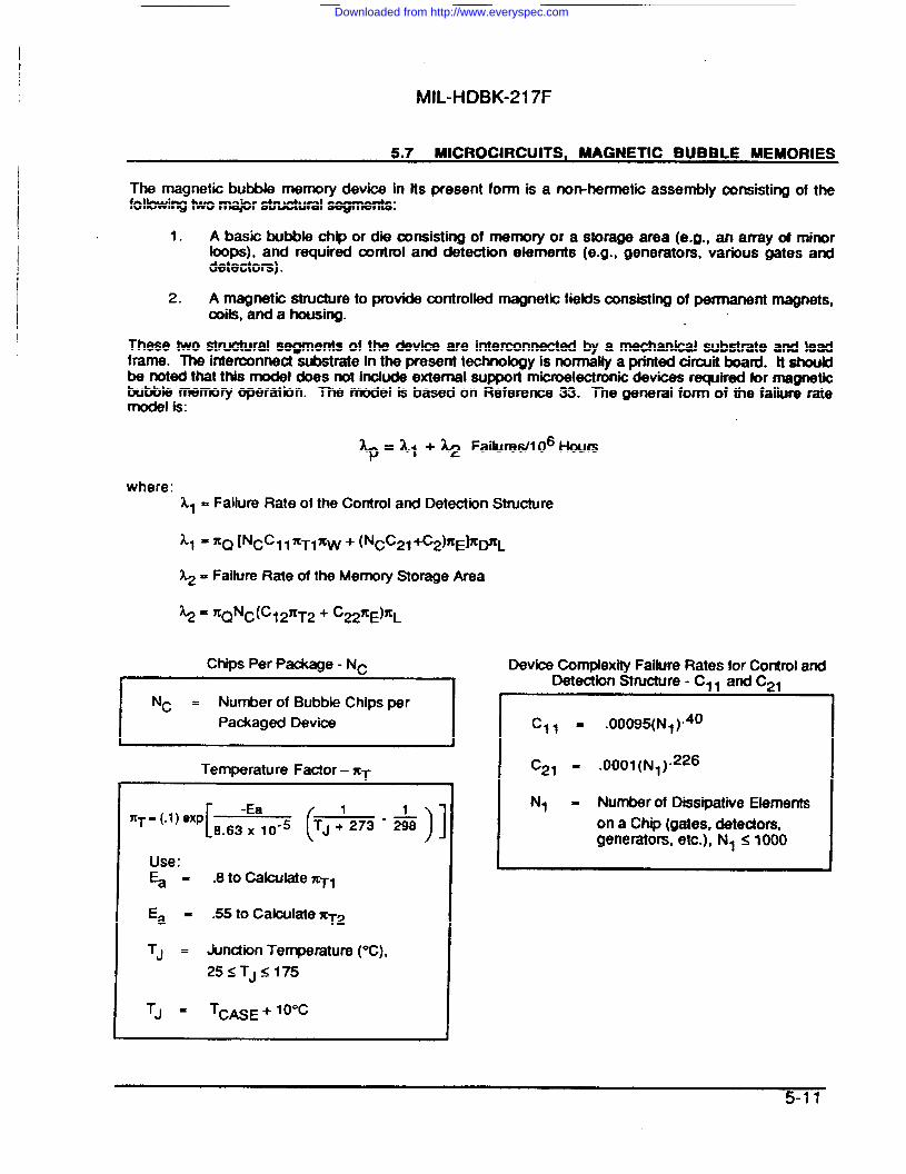
5.7 MICROCIRCUITS, MAGNETIC BUBBLE MEMORIES
The magnetic bubble memory device in its present form is a noMwnWic assembty consisting of thefolbwing two mapr structural segments:
1. A basic bubble chip or die consisting of memory or a storage area (e.g., an array of minorhops), and required control and detection elements (e.g., generators, various gates anddetectors).
2. A magnetic structure to provide controlled magnetic fields consisting of permanent magnets,coils, and a housing. .
These two structural segments of the device are intemcmnected by a mechanical substrate and leadframe. The interconnect substrate in the present technology is normally a printed cirwit bead. tt shoukfbe noted that this model does not inohde external suppmt microelectronic devices reqJired for magnetkbubble memory operation. The model is based on Reference 33. The general form of the fakwe ratemodel i s :
~= ~1 + ~ FaiJurest106 Hours
where:k, = Failure Rate of the Control and Detection Structure
~ = Failure Rate of the Memory Storage Area
ctips per Package - NR
Nc = Number of Bubble Chips perPackaged Device
Temperature Factor - XT
[
-Ea
(
1 1~T=(.l)@xp
8.63 X 10⁻⁵ TJ +273-= ) 1Use:% = .8 to Caloulate ?tTl
Ea = .55 to Calotdate *T2
TJ = Junction Temperature (°C),25 STJS175
TJ . TCASE + IO”C
Device Complexity Failure Rates for Control andDetectbn Stmcture - Cl, and C,l
c , , = .00095( N1)”40
C2, - .0001 (N1)”226
N, = Number of Dissipative Elementson a Chip (gates, detectors,generators, etc.), N, $1000
t w m m u
Downloaded from http://www.everyspec.com
MIL-HDBK-217F
5.7 MICROCIRCUIT, MAGNETIC BUBBLE MEMORIES
Write Duty Cycle Factor - ~
Zw = 1
D= Avg. Device Data Rate ~,Mfg. Max. Rated Data Rate
R/w= No.o fReads per Write
NOTE:For seed-bubble generators, divide~ by 4, or use 1, whkhever is greater.
D= Avg. Device Data Rate ~,Mfg. Max. Rated Data Rate
Device Complexity Failure Rates for MemoryStorage Sttucture -Cl ~ and C99
%2
C22
N2
= .00007(h@”3
s= .00001 (N2)”3
- Number of Bits, N2s 9 x 10⁶
AJlOther Model ParametersbParameter Section
I C5 I 5.9
5.10
5-12
Downloaded from http://www.everyspec.com
I
I&
MIL+IDBK-217F
S.8 MICROCIRCUITS, XT TABLE FOR ALL
-18
*
-1!!.
1I
5-13
—.————_z—————...—
Downloaded from http://www.everyspec.com
f
.,. ,! .-.
III 5.9 MICROCIRCUITS,
...!-..
MIL-HDBK-217F
C2 TABLE FOR ALL
IPackage Failure Rate for all Mhocircuits - C2
. —~. . xp”
Fbnnetb w%.w/Solder or Nonhermetic:
Number of Weld S@ Pin Dlf% ti Gtass Fk@adcs wtth Cans4 DIPs, mFunct”mnal Grid Array Sea? . Axiaf Leads on SMT (LeadedPins, Np (PGA)l, SMT 50 Mil Centers3 and
(Leaded and Nonleaded)5Nonkmded)
3 .00092 .00047 .00022 .00027 .00124 .0013 .00073 .00037 .00049 .00166 .0019 .0013 .00078 .0011 .00258 .0026 .0021 .0013 .0020 .003410 .0034 .0029 .0020 .0031 .004312 .0041 .0038 .0028 .0044 .005314 .0048 .0048 .0037 .0060 .006216 .0056 .0059 .0047 .0079 .007218 .0064 .0071 .0058 .008222 .0079 .0096 .0083 .01024 .0087 .011 .0098 .01128 .010 .014 .01336 .013 .020 .01740 .015 .024 .019
.025 .048 .032:: .032 .041128 .053 .068180 .076 .098224 .097 .12
1. c2=2.8 x 10+ (f$J ‘.m 2. c~ = 9.0 x 10⁻⁵ (N&1”51
3. C2 = 3.0 x 10⁻⁵ (N~l .= 4. C2 = 3.0 x 10⁻⁵ (N~2.01
5.1.08
C2 = 3.6 X 10+ (I$J
NOTES:
1. SMT: Surface Mount Technology
2. DIP: Dual In-Line Package
3. If DIP Seal type is unknown, assume glass
4. The package failure rate (C2) aocounts for failures associated only with the package itsetf.Failures associated with mounting the package to a circuit board are accounted for inSection 16, Interconnection Assemblies.
5-14
..= ..————————————
Downloaded from http://www.everyspec.com
MIL-HDBK-217FI
5.1O MICFIOCJRCUITS, %E,~L ANDxO TABLES FOR ALL
Envinmment Factor - ~Environment
%%%NSN“AC%F‘Uc*UFARWSFMFMLc1
%E
.502.04.0
4.06.04.05.05.08.08.0.50
5.012
220
Learning Factor - XLYears in Production, Y I 7CIs .1.51.01.5
2.01.81.51.2
XL= .01 e)(p(s.ss - .35Y)
Y = Years generic cfevice type has beenin production
Quality Faotors - ~Descrf@on I u
s~ . .
1: Procured in fufl accordancewith MIL-M-38!H O,Ciass Srequirements.
2. Procuraf in full accordance .25withMlL-+=3853smd~a B lherwo (Cfaae u).
3. Hybrids: (Procuredm Cfaaas requirements (Qualily L@vOlK) of MIL-H~.
1. Procured in full accordancewithMIL-M-3851 O,class Brequirements.
2. Procured m fut!accordance 1.0with MIL-I-38535, (Class Q).
3. Hybrids: Procured to Class Brequirements (QualityLevel1-f)ofMIL-H-3$534.
*
Fully compliant with allrequirements of paragraph 1.2.1d MIL-STD-883 and procured to a 2.0MIL drmving, DESC drawingordher government approveddocumentation. (Does not includehybrids). For hybrids use customscreening section below.
5-15
I T** & -- b--h -a--s -d.- ..—1 4 --- . . ——
Downloaded from http://www.everyspec.com
I .,. .,. ,, ..+.... . . . .
MIL-HDBK-217F
5.10 MICROCIRCUITS, %E, %L AND XQ TABLES FOR ALL—
Quality Factors (cent’cf):~ CdcUlation for CustomScreening ProgramsGroup MlL-STD-& Scmermeat (Note 3) Poinf Va)uatkm
TM 10IO(Ternperature Cycle, Cond BMinirmsm)and TM 2001(ConstantAcceleratbn, Cord B Minimum) and W 5004 (or 5008
1“ for Hybrids) (Finaf Electrkals @Te~E%trenws) and TM 1014 50(Seal Test, Cond ~ B, or C) and TM 2009 (External Visual)TM 1O1O (Terrqmature Cycle, Cond B Minimum) or TM 2001(Constant Acceleration, Cond B Minimum)
2* TM 5004 (or 5008 for Hytxlds) (Fhal EkOtca& @ Terrp Extremes) 37and TM 1014 (Seal Test, Cond A, B, orC) and TM 2009 (Externalvisual)Pre-Bum in Electrkals
3 TM 1015 (Bum-in B-LeveVS-Level) and TM 5004 (or 5008 for 30 (B Level)(Post Burn-in ElectdcaJs @ Te ~ Extremes) 36 (S Level)
4* Th42020Pirld(PaRi0fe fmpaothJ0ie0 ~) 11
5 TM 5004 (or 5008 for Hybrids) (Final Electricats @ Te~rature 11 (Note 1)Extremes)
6 TM 2010/17 (internal Visual) 7
7* TM 1014 (Seal Test, Cond A, B, or C) 7 (Note 2)
8 TM 2012 (Radiography) 7
9 TM2009 (ExternalVisual) 7 (Note2)
10 TM 5007/5013 (GaAs) (Wafer Acceptance) 1
11 TM 2023 (Non-Destructive Bond Pull) 1
87ZQ =2+
Z Point Valuations
●NOT APPROPRIATE FOR PIJWTIC PARTS.
NOTES:1. Point valuation only assigned if used independent of Grwps 1, 2 or 3.2. Point valuatbn onty assigned if used independent of Groups 1 or 2.3. Sequencing of tests within groups 1, 2 and 3 must be followed.4. TM refers to the MIL-STD-883 Test Method.5. Nonhermetk pafis should be used onty in controlled environments (i.e., GB and other
temperaturelhumldtty controlled environments).
EXAMPLES:
1. 87Mfg. performs Group 1 test and Class B bum-in: ~ Q = 2 + _ = 3.1
7 87-. Mfg. performs infernal visual test, seal test and final electrical test: ~ Q = 2 + ~ = 5.5
Other Commercial or Unknown Screening Levels f i Q = 10
5-16
.—___ . —
Downloaded from http://www.everyspec.com
—-
., .,.
MIL-HDBK-217F
5.11 h81CROClRCU?TS, 7.s DETERMINATION, (ALL EXCEPT HYBRIDS]
Ideally, device case temperatures should be determined from a detailed thermal analysis of thewmm. NV* @wtion temperature is then calculated with the fofbwing relationship:
.. TJ . Tc + OKP
TJ = Worst Case Ju~ion Tempemture ~C).
Tc = Case Temperature (oC). If not avaiM#e, w the Wlowing default tatlb.
Default Case Tempemture (T~ for all Environments
TC (“C) I 35 45 50 60 60 75 75 60 I 35 50 60 45 I
(3JC = Junction-toese thermal resistance (°CAwtt) for a device soldered into a printed circuitboard. If OK is not available, use a Vabe contained in a specification for the closestequivalentdevke or use the following tabJe.
Die Area >14,400 m~ ew Die Areas 14,400 rni?Package Type(ceramic only) (w 8JC (~
Dual-in-Lm 11 28Flat Package 10 22Chip Carner 10 20Pin Grid Array 10 20Can 70
P = The maximum power dmtion realized in a systemappficatiin. If the applied power isnot available, use the maxknum power dissipationfromthe specificationfor the closestequivalent device.
Downloaded from http://www.everyspec.com
MIL-HDBK-217F
5.12 MICROCIRCUITS, T-l DETERMINATION, (FOR HYBRIDS) —
This sectbn descrfbes a method for estimating junction temperature (TJ) for integrated circuit dke
mounted inahybrkfpackage. A~k~~mti~timormrew-e~-tiWwithin a sealed package. Each substrate assetity consistsof active and passive chips with thickorthinfilm metallization mounted on the substrate, whii in turn may have multiple layers of metallization and
dielectric on the surface. Figure 5-1 is a cross-sectional view of a hybrid with a single multi-layered
substrate. The layers within the hybrid are made up of various materials with different thermal
characteristics. The table folbwlng Figure 5-1 provkles a llst of commonly used hybrid materials with
typical thicknesses and comesponding thermal conductivtties (K). If the hybrid internal structure cannot be
determined, use the following default values for the temperature rise from case to junction: miomdrculs,1O“c; transistors, 25%; diodes, 20W. kalJrm ~ are at Tc.
CHIP (A)
\~LID
CHIP ATJACH (B) .
INSULATING I
LAYER (C)
mSUBSTRATE (D)
MATERIALTHICKNESS, L i PACKAGE
EPOXY (E) LEAD
CASE (F)
Figure 5-1: Cross-sectional View of a Hybrtd with a Single Multl-Layered Substrate
5-18
Downloaded from http://www.everyspec.com
MIL-HDBK-217F
5.12 MICROCIRCUITS, T-l DETERMINATION, (FOR HYBRIDS)
Tvkal Hvbrid Characterktii
Conductivity,Typkal Feature Ki IL
Material Typical U!wge Thickness, From Figure
() (W/in* ()()Ki i
+ (in.) 5-1 .Win in2 oC/W
Silicon Chip Device 0.010 A 2.20 .0045
chip Devbe 0.0070 A .76 .0092
Au Eutectic Chip Attach 0.0001 B 6.9 .000014
Solder Chip/Substrate Attach 0.0030 B/E 1.3 .0023
Epoxy (Dielectric) Chip/Substrate Attach 0.0035 BIE .0060 .58
Epoxy (Conductive) Chii Attach 0.0035 B .15 .023
Thck Film Dielectric Gl= Insubthg Layer 0.0030 c .66 .0045
Alumina Substrate, MHP 0.025 D .64 .039
Beryllium Oxide Substrate, PHP 0.025 D 6.6 .0038Kovar Case, MHP 0.020 F .42 .048
AJuminum Case, MHP 0.020 F 4.6 .0043
Copper Case, PHP 0.020 F 9.9 .0020
NOTE: MHP: Muftichip Hybrid Package, PHP: Power Hybrid Package (Pwc > 2W, TypicaUy)
;1(*)(‘i)em= = A
n = Number of Material Layefs
Ki z()W/in*Thermal Conductivity of ith Material ~ (User Provided or Fmm Table)
Li = Thiiness of im Material (in) (User Provided or From Table)
A = Die Area (inz). If Die Area cannot be readity determined, estimate as follows:A = [ .00278 (No. of DB Active Wire Terminals) + .041#
Estimate TJ as Folk)ws:
TJ = Tc + .9 (e~ (p~
Tc =
eJ~ =Pf) =
Hybrid Case Temperature (“C). If unknown, use the Tc Defautt Table shown in Section 5.11.
Junction-to-Case Thermal Resistance (°C/W) (As determined above)Die Power Dissipation (W)
5-19
Downloaded from http://www.everyspec.com
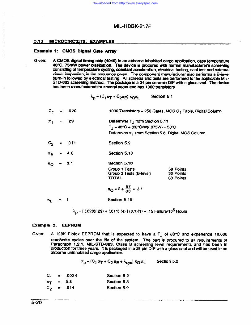
MIL-HDBK-217F
5.13 MICROCIRC UIT& EXAMPLES
Example 1: CMOS Dlgftal Gate Array
Given: A CMOS digitaltiming ~ (4048) in an ahborne inhabitedcargo applkxdbn, case temperature4Y’C, 75mW power deefpatim The device is pmwrad with normal marndacturetsscreeningconsisting of terrperature oycflng, oomtant aooeleratbn, electrical testing, seal test and externalvisual Owpectkm, in the seqMnce given. The oorrponent manufacturer also performs a B-1evelbum-in folbwed by electrical testing. AU screens and tests are performed to the applicable MIL-STD-883 screening method. The package is a 24 pin oeramic DIP with a glass seal. The devicehas been manufactured for severaf years and has 1000 transistors.
Section 5.1
c1 = .020
XT = .29
c~ = .011
?tE = 4.0
7CQ = 3.1
1000 Transistor -250 Gates, MOS Cl Table, Digital Column
Determ\ne TJ from Sectbn 5.11TJ = 48W + (28”@W)(.075w) = 50WDetermine ~T from Section 5.8, Digital MOS Column.
Section 5.9
Section 5.10
Seotion 5.10Group 1 TestsGroup 3 Tests (Blevel)TOTAL
50 Points
80 Points
XL = 1 Section 5.10
~= [ (.020)(.29) + (.011) (4)] (3.1)(1)= .15 Failure/106 l-lows
Example 2: EEPROM
Given: A 128K Flotox EEPROM that is expected to have a TJ of 80”C and experience 10,000readhmite cycles over the life of the system. The part is procured to all requirements ofParagraph 1.2.1, MIL-STD-883, Class B screenin
7level requirements and has been in
productbn for three years. tt b packagd in a 26 pin D P with a glass seal and will be used In anairborne uninhabited oargo application.
~=(ClXT+C2YCE+~)nnL Sectbn 5.2
c1 = .0034 Section 5.2XT = 3.8 Section 5.8C2 = .014 Section 5.9
Downloaded from http://www.everyspec.com
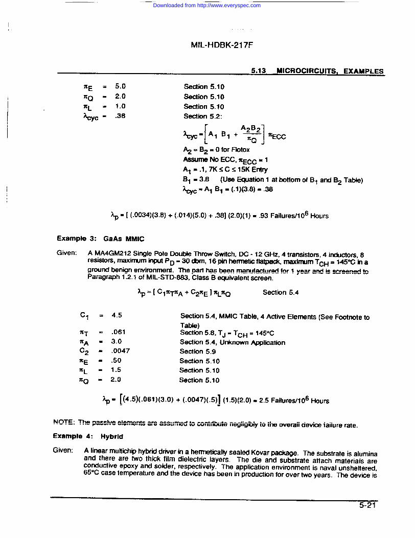
MIL-HDBK-217F
(
I
I
5.13 MICROCIRCUITS, EXAMPLES
~E = 5.0 Section 5.10I C Q = 2.0 Section 5.10XL ~ 1.0 Section 5.10
b c= .38 Section 5.2:
A2B*%[ 1=AIB1+~~~
~ = f32 = Ofor Fiotox~ No ECC, %ECC = 1A,=.l,7Ksc s15KEntry81 .3.8 (Use Equation 1 at bottom of B1 and ~ Tabie)
~~ = ‘1 B, = (-1)(3.8) = .38
~= [ (.0034)(3.8) + (.014)(5.0)+ .38] (2.0)(1)= .93 Failures/106 Hours
Example 3: GaAs MMIC
Given: A MA4GM212 Single Pole Double Throw Switch, DC -12 GHz, 4 transistors, 4 inductors, 8resistors, maximum Input PD = 30 ~, 16 pin hermetio flatpack, maxirrum TCH = 14WC m aground benign environment. rne part has been manufactured for 1 year and is screened toParagraph 1.2.1 of MIL-STD-883, Class B equivalent soreen.
Seotion 5.4
c1 =
%E =
XL =
7FQ -
4.5 Section 5.4, MMIC Table, 4 Active Elements (See Footnote toTabie)
.061 Section 5.8, TJ = TCH = 145°C3.0 Section 5.4, UrhOwn Application.0047 Section 5.9.50 Section 5.101.5 Section 5.102.0 Section 5.10
~= [(4.5)( .061) (3.o) + (.0047)(.5)] (1.5)(2.0) = 2.5 Failures/106 Hours
NOTE: The passive elements are assumed to contribute negligibly to the overall device failure rate.
Example 4: Hybrid
Given: A linear muttichip hybrid driver in a hermetically sealed Kovar package. The substrate is aiumina
and there are two thi@ film dielectric layers. The die and substrate attach materials areconductive epoxy and soider, respectively. The application environment is navai unsheltered,65°C case temperature and the device has been in production for over two years. The device is
5-21
Downloaded from http://www.everyspec.com
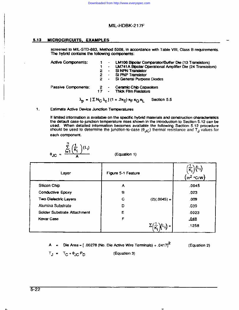
MIL-HDBK-217F
5.13 MICROCJRCUJTS, EXAMPLES
screened to MIL-STD-883, Method 5008, in accmkwxe with Table Vlll, Class B requirements.The hybrid contahw the followhg components:
Active Components: 1-1-2-2-2-
Passive Components: 2 -17 -
LMl 06 Bipolar Co~rator-er Die (13 Transistors)LM741A Bipolar Operational Arnpliir Die (24 Transistor)S NPN TransistorSi PNP TmnsistorSi General Purpose Diodes
Cerwlb c~ CapacitorsThick FItm Resistors
+ -~E) %F~ ~ Sectbn 5.5
1. Estimate Active Device Junction Terrperatures
If limited informationis available on the specific hybtid materials and construction characteristicsthe defautt case-to-junction temperature rises shown in the introduction to Section 5.12 can beused. When detailed information becmmes available the following Section 5.12 procedureshoukf be used to determine the junction-to-case (tlJc) thermal resistance and TJ vatues foreach component.
,,c =wA (Equatbn 1)
()()~ Li
KiLayer Fgure 5-1 Feature
in2 OC/W
Silicon Chip A .0045
Conductive Epoxy B .023
Two Dielectric Layers c (2)(.0045) = .009
Alumina Substrate D .039
Solder Substrate Attachment E .0023Kovar Case F
A = Die Area= [ .00278 (No. Die Active Wire Terminals) + .0417J2 (Equation 2)
TJ = Tc + OJC ‘D (Equation 3)
5-22
Downloaded from http://www.everyspec.com
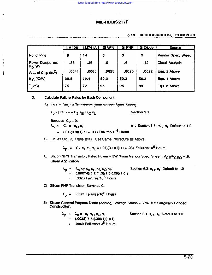
—
MIL-HDBK-217F
5.13 MICROCIRCUITS, EXAMPLES
LM 106 LM741A Si NPN
No. of PinsI
8I14
I3
Power Dissipation, .33 .35 .6pD (W)
Area of Chpjin.2) .0041 .0065 .0025
e~ (w 30.8 19.4 50.3
‘J (~) 75 72 95
s PNP lSi Diode’ Source
3
II2 Vendor Spec. Sheet
.6 .42 CircaJitAnalysis
.0025 .0022 Ey. 2 Above
50.3 56.3 Equ. 1 Above
95 89 Ew. 3 Above
2. Calculate Failure Rates for Each Corrqmnent:
A)
B)
c)
LM106 DM, 13 Transistors (from Vendor Spec. Sheet)
~=[c,q+c~Yc~l~Qq Section 5.1
Because C2 = O;
‘P = Cl XT ~ Q XL ~T: s-h 5.8; ~ Q , ZL Default tO 1.0= (.01)(3.8)(1)(1) = .038 Failures/106 Hours
LM741 Die, 23 Transistors. Use Same Procedure as Above.
$= Cl XT Z* XL = (.01)(3.1)(1)(1) = .031 Failures/106 Hours
Silicon NPhl Transistor, Rated Power= 5W (From Vendor Spec. Sheet), Vc#VCEO = .6,Linear Application
~ = %“PA’R%KQ’E s8CtiOn 6.3; ZQ, ~E Defautt to 1.0= (.00074)(3.9)(1 .5)(1 .8)(.29) (l)(1)
D)
E)
= .0023 Failures/l 06
Silicon PNP Transistor, Same as C.
Silicon GeneralConstruction.
.0023 Failures/106
Hours
Hours
Purpose Diode (Anabg), Vottage Stress= 60%, Metallurgically Bonded
%’T%~nQ% Section 6.1; nQ, XE Default to 1.0(.0038)(6.3)(.29)(1)(1)(1).0069 Failures/l 06 Hours
5-23
I ,. 1
Downloaded from http://www.everyspec.com
I
[
. . .. . . .
MIL-HDBK-217F
I
5.13 MICROCIRCUITS, EXAMPLES .
F) Ceramic ChipCapacitor,VoltageStress= 50%.,‘A “ ‘CASE for the Hybrid, 1340 pF, 125°C Rated Tenp
% = %%V%)’E Section= (.0028)(1.4)(1)(1)= .0039 Faitures/106 Hours
10.1 1; xQ, fiE Default to 1.0
G) Thiok Film Resistors, per kwtructbns in Section 5.5, the contribution of these devices isconsidered insiinifiint relative to the overall hybrid failure rate and they maybe ignored.
[XbJc~c](l+2@ItF~q
6.0 Section 5.105.8 Section 5.51 Section 5.101 Section 5.10
[ (1)(.038)+ (1)(.031)+ (2) (.0023)+ (2) (.0023)
+ (2)(.0069) + (2)(.0039) ](1 + .2(6.0)) (5.8) (1)(1)
1.3 Failures/l 06 Hours
5-24
Downloaded from http://www.everyspec.com
f... . . . . . . . . . .. . . . . . . . . .. ..— .- ..!.
MIL-HDBK-217F
6.0 DISCRETE SEMICONDUCTORS, INTRODUCTION
II
I
The semiconductor tmnsistor, dbde and opto-electronic devke sections present the faWe rates onthe basis ofdevketypeand cmstwtbn. An mafytbd -I of the talbre rate is also presented for eachdevke category. The various types of dkcrete semkmductor devkes require different failure ratemodels that vary to some degree. The models apply to single devices unless otherwise noted. Formh**v-rn as@k_t~~ti h~ti5.5*Mb Md.
The applicable MIL specification for transistors, and optoelectronk devices is MIL-S-19500. Thequality levels (JAN, JANTX, JANTXV) are as defined in MIL-S-19500.
The t~p9mtWt3 faCtOr (%T) is based on the devke jumtbn temperature. Junctbn temperatureshould be oomputed based on worse case power (or maxhmm power c!ksipatbn) and the device junctionto ease thermal resktanoe. Determinatbn of junction temperatures is explained in Section 6.14.
Refererwe 28 should be consulted for further detailed information on the mode!s appearing in thissection.
6-1
1
Downloaded from http://www.everyspec.com
MIL-HDBK-217F
I 6.1 DIODES, LOW FREQUENCY —
SPECIFICATION DESCRIPTIONMlL-S-l 9500 @ Frecpxmqr D-s: General Putpse Analog, Switch~
Fast Rewvery, f%wer RecWer, Tmsient S~r, CurrentRegulator, Vol@e Regulator, Voltage Reference
Lp = &##czQzE Failures/l OG Hours
Base Failure Rate - &Diode Type/Appiicatbn “ ~
General PuqxM Analog .0038switching .0010Power Redfiir, Fast Recovery .069Power Rectifier/Schottky .0030Power DiodePower Rectifier with .0050/HigiI Voltage Stacks Junction
Transient Suppressor/Vanstor .0013Current Reguiator .0034Voltage Regulator and Voltage .0020Reference (Avaiancheand Zener) I
i
Terrperature Factor - XT(General Purpose Analog, Switching, Fast Recovery,
PoulTJ (’C)
253035404550556065707580859095100
r Rectifier,TIXT
1.01.21.41.61.92.22.63.03.43.94.45.05.76.47.28.0
dent Su-pgmTJ ~C)
105110115120125130135140145150155160165170175
isor)XT
9.01011121415161820212325283032
((-3091 1 1XT = exp TJ + 273))
-Z&
TJ - JunctionTemperature (“C)
Temperature Factor - q(VOitag. Regulator, Voitqo Rdormce,
h cun’UWRncddYW)—.- ---- . ... . -~---. #TJ (“C) %T ‘J (’=) v
25 1.0 105 3.930 1.1 110 4.235 1.2 115 4.540 1.4 120 4.845 1.5 125 5.150 1.6 130 5.455 1.8 135 5.760 2.0 140 6.065 2.1 145 6.470 2.3 150 6.775 2.5 155 7.180 2.7 160 7.585 3.0 165 7.990 3.2 170 8.395 3.4 175 8.7100 3.7
((
1 1%T = exp -1925 TJ +273-=))
TJ . JunctionTemperature (oC)
6-2
Downloaded from http://www.everyspec.com
+. .,
MIL-HDBK-217F
6.1 DIODES, LOW FREQUENCY
Electrical Stress Factor - ZSStress I 7CS
Transient Suppressor,Voltage Regulator, VoltageReference, CurrentRegulator 1.0
All Others:v~ s .30 0.054.3 c v~ s .40 0.11.4< Vs s .50 0.19.5<v#60 0.29.6< Vs s .70 0.42.7< V~ s .80 0.58.8< V~ s .90 0.77.9<v#. oo 1.0
For All Except Transient Suppressor, Voltage
Regulator, Voltage Reference, or CurrentRegulator
7CS= .054 (Vs s .3)
~s = v~2.43 (.3 < v+ 1)
Voltage Applied~~ = Voltage Stress Ratio = Voltage Rated
Voltage is Diode Reverse Voltage
Contact Construction Factor - xcContact Construction I I@
Metallurgically BondedI
1.O
Non-Metallurgically Bonded and I 2.0Spring Loaded Contacts
Quality Factor - X(Quality
JANTXV
JANTX
JAN
Lower
Plastic
tcQ
0.7
1.0
2.4
5.5
8.0
Environment Factor - ZEEnvironment 7tE
GB 1.0
GF 6.0
% 9.0
N~ 9.0
Nu 19
‘Ic 13
‘IF 29
*UC 20
‘UF 43
‘RW 24
SF .50
MF 14
ML 32
CL 320
6-3
Downloaded from http://www.everyspec.com
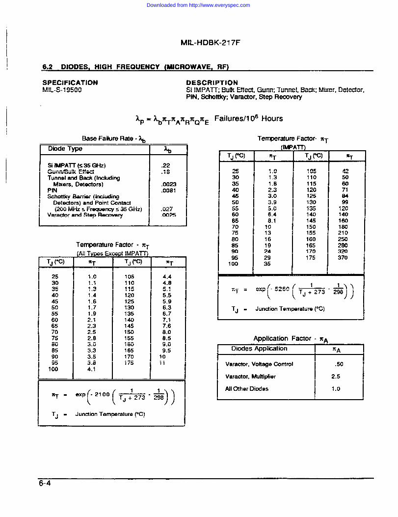
MIL-I+DBK-217F
6.2 DIODES, HIGH FREQUENCY (MICROWAVE, RF)
SPECIFICATION DESCRIPTIONMlL-S-l 9500 Si IMPA7T; Buk Effect, Gunn; Tunnel, Back; Mixer, Detector,
PIN, Schottky; Varactor, Step Recovery
Base Failure Rate - ~Dbde Type h
Si lMPAIT (s 35 GHz) .22Gunn/Bulk Effect .18Tunnel and Bd (includingMixers, Detectors) .0023
PIN .0081Schottky Barrier (includingDetectors) and Point Contact(200 MHzs Frequenqs 35 GHz) .027
Vamctor and Step Recovery .0’025
Temperature Factor - q(All Types Excq)t IMPA7T)
TJ (“C) XT TJ (oC)
25 1.0 105 4.430 1.1 110 4.835 1.3 115 5.140 1.4 120 5.545 1.6 125 5.950 1.7 130 6.355 1.9 135 6.760 2.1 140 7.165 2.3 145 7.670 2.5 150 8.075 2.8 155 8.580 3.0 160 9.085 3.3 165 9.590 3.5 170 10
3.8 175 111: 4.1
((-2100 1 1
XT = exp))
TJ +273-~
TJ = JunctionTemperature (“C)
Failures/l 06 Hours
TJ ~)
25303540455055606570758085
z100
Tenqxmtum Factor- %T
1.01.31.82.33.03.95.06.48.110131619242935
105110115120125130135140145150155160165170175
4250
E8499120140160180210250280320370
((-5260 1 1‘T = exp TJ + 273 -Zz
))
TJ = JunctionTemperature (“C)
Application Factor - fiADiodes Application I ~A
Varactor, Voltage Control .50
Varactor, Mu?tip!ier 2.5
AllOther Diodes 1.0
6-4
Downloaded from http://www.everyspec.com
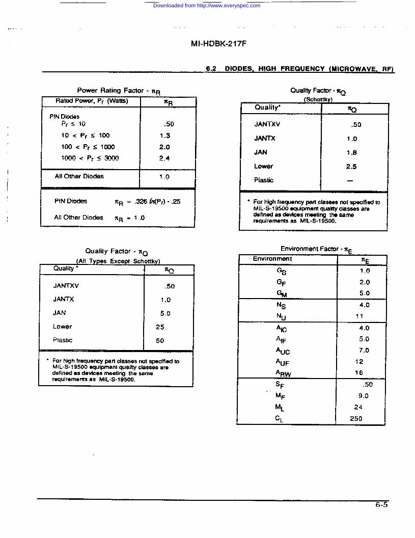
,,. . ,.
MI-HDBK-217F
.- .-.
6.2 DIODES, HIGH FREQUENCY (MICROWAVE, RF)
Power Rating Factor - XR Quality Factor - ~Rated Power, Pr (Watts) (Scha
Quaiity’
JANTXV
JANTX
JAN
Lower
Plastic
ky)
%
.50
1.0
1.8
2.5
PIN Diodesp~ < 10
10 < Pr s 100IOO<Pr Sl~
1000 <Pr S3000
.50
1.3
2.0
2.4
All Other Diodes 1.0
Pthl Diodes Iqq = .326 k(Pr) -.25
All Other Diodes XR = 1 .0
● For highfrequency part classes notspecifiedtoMlL-S-l 9500 equipmentqualityclassesaredefinedae devicesmeeting ths Samerequirementsas MlL-S-l 9500.
Environment Factor - z=Quaiity Factor - nQEnvironment
GB
GF
%Ns
Nu
Ac
‘IF
*UC
‘UF
‘RWSF
. .MF
ML
CL
~E
1.02.0
5.0
(All Typas Except SclI Quality” t
I
JANTXV
JANTX
JAN
Lower
Plastic
.50
1.04.0
115.0
25 4.0
5.0
7.0
12
16
50
● For high frequency part classesnotspedfied toMl L-S-l 9500 equipmentqualhyclassesaredefinedas devbes meeting the sameraqulrementsas MlL-S-l 9500.
.50
9.0
24
250
6-5
Downloaded from http://www.everyspec.com
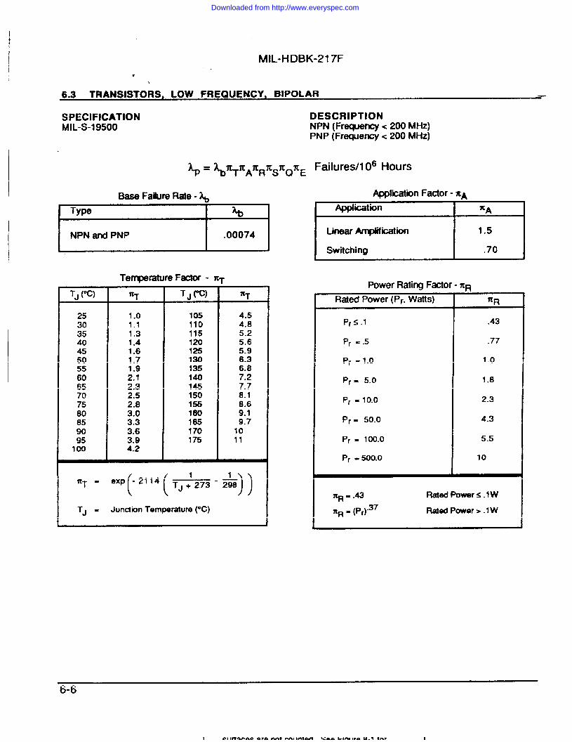
MIL-HDBK-217F●
✎✎
6.3 TRANSISTORS, LOW FREQUENCY, BIPOLAR —
SPECIFICATIONMIL-S-19500
Ap =
DESCRIPTIONNPN (Frequency< 200 MHz)PNP (Frequency< 200 MHz)
%? ‘AXR%ZQXE Failures/l 06 I-loufs
Base Failure Rate - ~
I Type I h
I NPN and PNPI
.00074
TJ (*) XT TJ (“C) - %T
25 1.0 105 4.530 1.1 110 4.835 1.3 115 5.240 1.4 120 5.645 1.6 125 5.950 1.7 130 6.355 135 6.860 ;:: 140 7.2
145 7.7% 5:: 150 8.175 2.8 155 8.680 3.0 160 9.1
165 9.7E ::: 170 1095 3.9 175 11100 4.2
((-2114 1 1XT = exp TJ + 273 -=
))
TJ = Junclbn Temperature (“C)
Application Factor - %AApplication I %A
Linear Ampliiicatiorl
Switching
1.5
.70
Power Rating Factor - ZRRated Power (Pr, W~S)
Pr~ .1
Pr = .5
Pr =1.0
Pr = 5.0
Pr = 10.0
Pr = 50.0
P~ = 100.0
Pr -500.0
. .?tR
.43
.77
1.0
1.8
2.3
4.3
5.5
10
I
%-. * Rated Powers .lW
~ - (Pr).37 RatedPower >.1 W
6-6
I .l@ I -
Downloaded from http://www.everyspec.com
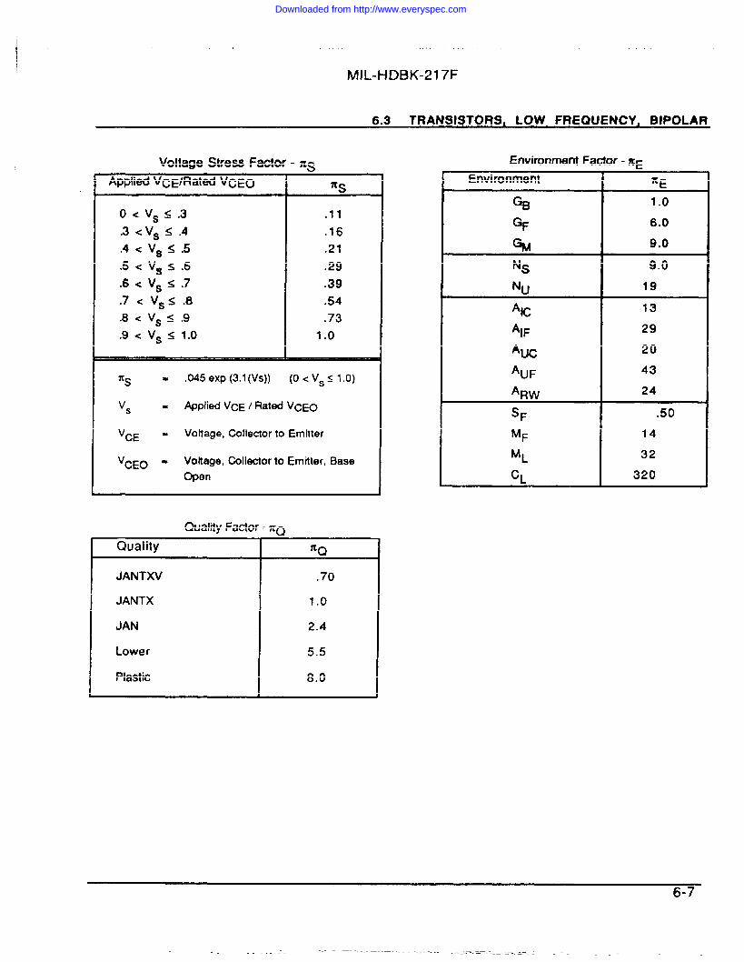
.
MIL-HDBK-217F
I
6.3 TRANSISTORS, LOW FREQUENCY, BIPOLAR
Voltage Stress Factor - YCSApplied vCE/Rabd VCEO - ~~
o<v #.3 .11.3<v~s.4 .16.4<v @.5 .21.5c V~S.6 .29.6< V#.7 .39.7<v @.0 .54.8< V#.9 .73.9< v~ s 1.0 1.0
—~~
% - ,045 exp (3.1(vS)) (o<v#l.o)
v~ . Applied VCE / Rated VGEO
VCE = Voltage, Collector to Emitter
‘CEO - Voltage, Colleotor to Emitter, BaseOpen
Quality Factor - ZQ
Quality I 7c~
JANTXV .70
JANTX
JAN
Lower
Plastic
1.0
2.4
5.5
8.0
Erwironment Factor - ~FEnvironment %E
GB 1.0
GF 6.0
% 9.0
Ns 9.0
N“ 19
AC 13
‘IF 29
AM 20
‘UF 43
‘RW 24
SF .50
MF 14
ML 32
CL 320
6-7
Downloaded from http://www.everyspec.com
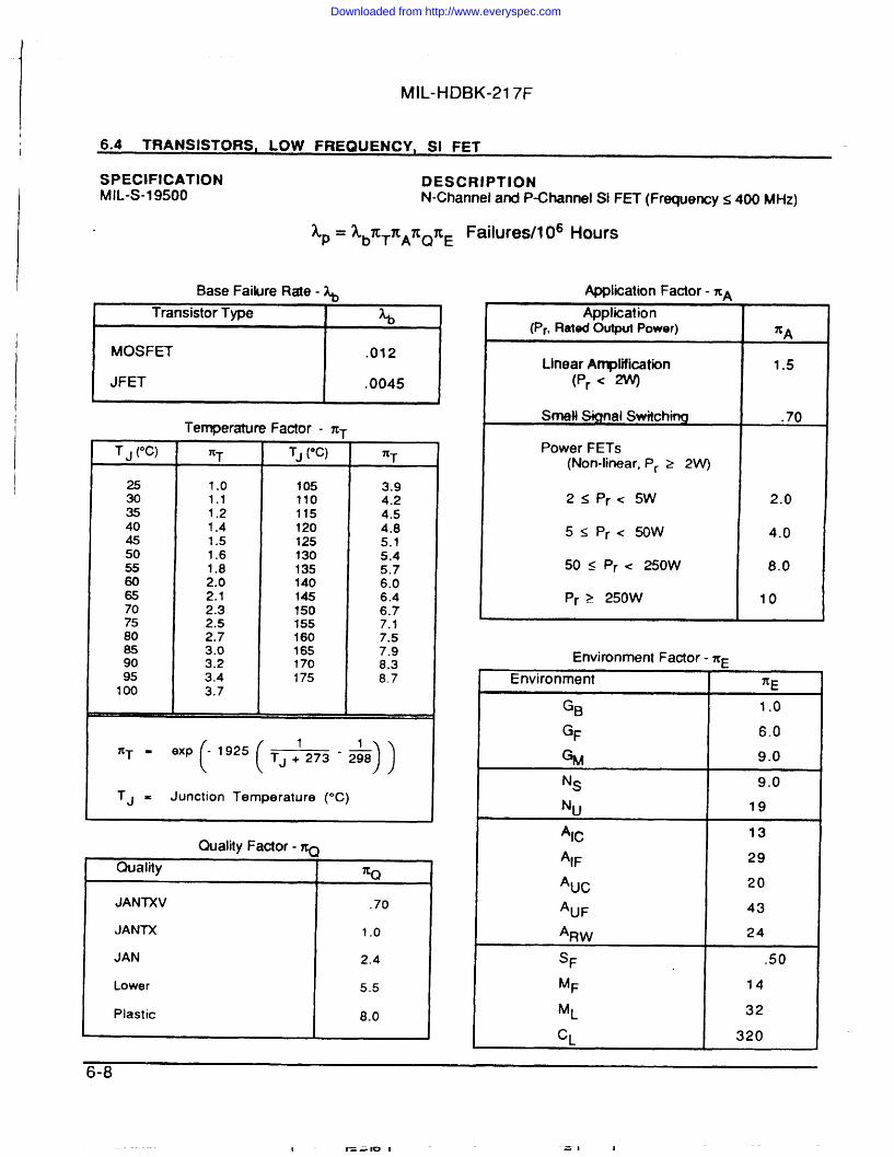
MIL-HDBK-217F
6.4 TRANSISTORS, LOW FREQUENCY, SI FET
SPECIFICATION DESCRIPTl ONMIL-S-19500 N-Channel and P-Channel Si FET (Frequencys 400 MHz)
Ap = kb7cT7cA7tQ7cE
Base Failure Rate - ~●
Transistor Type %
I MOSFET
JFET I :::5ITemperature Factor - n~
T ~ (“C) *T TJ (“C) XT
25 1.0 1051.1 110 ::;
E 1.2 115 4.540 1.4 120 4.845 1.5 125 5.150 1.6 130 5.455 135 5.760 ;:: 140 6,065 2.1 145 6.470 2.3 150 6.775 2.5 155 7.180 2.7 160 7.585 165 7.990 u 170 8.395 3.4 175 8.7100 3.7
* A
((
1nT = 1exp - 1925 TJ + 273 -izii))
TJ = Junction Temperature (“C)
Quality Factor - ~Ouality 7CQ
JANTXV .70
JANTX 1.0
JAN 2.4
Lower 5.5
Plastic 8.0
Failures/l 06 Hours
Application Factor - ~AApplication
(Pr, Rated Output Power)
Linear Amplifkxtion(Pr < W)
small S@rlal Switching
Power FETs(Non-linear, Pr z 2W)
2< Pr<5W
5<Pr<~W
50 s Pr < 250W
Pr > 25OW
Environment Factor - x=
.70
2.0
4.0
8.0
10
I Environment I xc
GB 1.0
GF 6.0
GM 9.0
NS 9.0
Nu 191Alc 13
‘IF 29
*UC 20
*UF 43
*RW 24
SF .50
MF 14
ML 32
CL 320
b-U
I 1=-IO I =1 I
Downloaded from http://www.everyspec.com
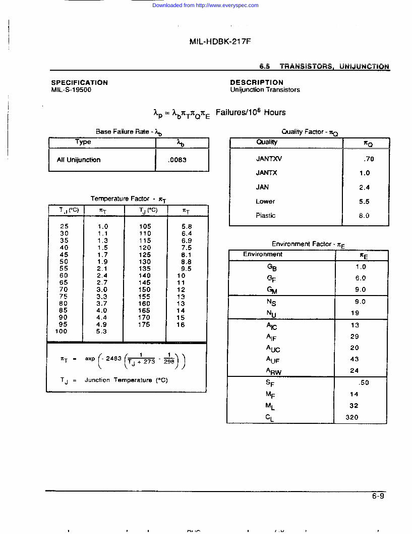
MIL-HDBK-217F
6.5 TRANSISTORS, UNLIUNCTION
SPECIFICATIONMIL-S-19500
Lp = kb7cT7TQ7cE
Base Failure Rate - ~
All UnijuntilonI
.0083I
Temperature Factor - XT
T ~ (“C) ~T TJ (“C) XT
25 1.0 105 5.830 1,1 110 6.435 1.3 115 6.940 1.5 120 7.545 1.7 125 8.150 1.9 130 8.855 2.1 135 9.560 2.4 140 1065 2.7 145 1170 3.0 150 1275 3.3 155 1380 3.7 160 1385 4.0 165 1490 4.4 170 1595 4.9 175 16100 5.3
((-2483 1 1nT = exp TJ + 273 -m
))
TJ = Junction Temperature (°C)
DESCRIPTIONUnijunction Transistors
Failures/l OG Hours
Quality Factor - ~Quality
JANTXV
JANTX
JAN
Lower
Plastic
Environment Factor - XEEnvironment
GB
GF
%/l
Nu
AC
‘IF
‘Uc
*UF
*RWSF
MF
ML
CL
%Q
.70
1.0
2.4
5.5
8.0
—%E
1.0
6.0
9.0
9.0
19
13
29
20
43
24
.50
I
32
L
6-9
I I <1 I
Downloaded from http://www.everyspec.com
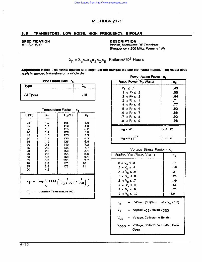
4
MIL-HDBK-217F
6.6 TRANSISTORS, LOW NOISE, HIGH FREQUENCY, BIPOLAR
SPECIFICATION DESCRIPTIONMIL-S-19500 Bipolar, Micmvave RF Transistor
(F~ency >200 MHz, Power< lW)
kp = ‘b~z#&QKE Failures/l 06 Hours
Applkatlon Note: The model applies to a single die (for multiple die use the hybrid model). The model doesapply to ganged transistors on a single die.
Base Failure Rate - &I
1 I—
I I
I All TypesI
,18I
Temperature Factor - q
TJ (“C) XT TJ W) - XT
25 1.0 105 4.530 1.1 110 4.835 1.3 115 5.240 120 5.645 ;:; 125 5.950 1.7 130 6.355 6.860 ;:: :Z 7.265 2.3 145 7.770 2.5 150 0.175 2.8 155 8.680 3.0 160 9.185 3.3 165 9.7
3.6 170 10E 3.9 175 11100 4.2
((-2114 1 1
XT = exp TJ +273-=))
TJ = JunctionTemperature (oC)
Power Rating Factor - Xn. .R~6d ~ (Pr, W~S) %R
Pr < .1 .43.l<Pr 5.2 .55.2< PrS.3 .64.3< Pr $.4 .71.4< PrS.5 .77.5< Pr~.6 .83.6< PrS.7 .88.7< PrS.8 .92.8< Pr <.9 .96
7KR..43 P~ S.lw
~ = (Pr )“37 Pr >.lWI
Voltage Stress Factor - x~Applied VCE/R~ed VCEO %
o<v #.3 .11.3 <V=s .4 .16.4<v #.5 .21.5< V#.6 .29.6< V8S.7 .39.7< VSS .8 .54.8<v~s.9 .73.9< v~ s 1.0 1.0
% - .045 exp (3.1(vS)) (o< v~ s 1.0)
v~ - AppliedVCE / Rated VC~
v= - Vottage, Collectorto Emitter
‘CEO = Voltage, Collector to Emitter, BaseOpen
I I
Downloaded from http://www.everyspec.com
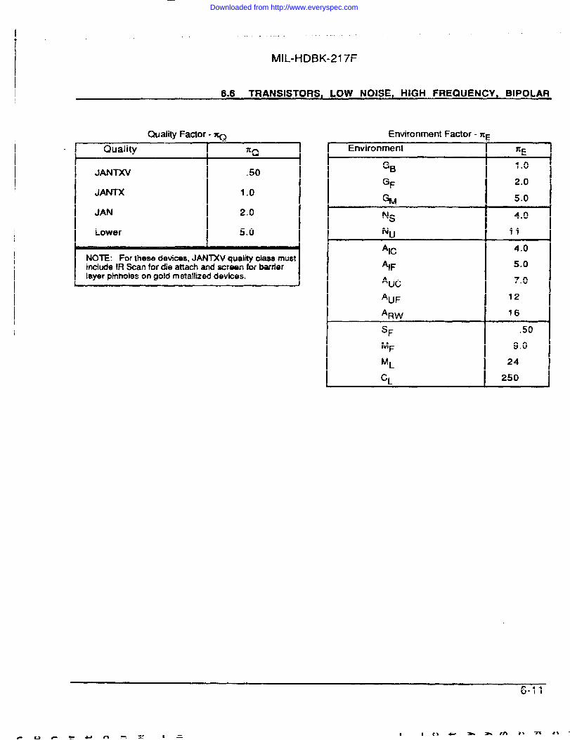
,, . .. !.,
MIL-HDBK-217F
6.6 TRANSISTORS, LOW NOISE, HIGH FREQUENCY, BIPOLAR
Quality Factor - ~
Quality 7tQ
JANTXV .50
JANTX 1.0
JAN 2.0
Lower 5.0
NOTE: For these devices, JANIXV quatii class mustinciude IR Scan for die attach and scraan for barrierlayer pinhotes on gold metallized devices.
Environment Factor - ~FEnvironment ~E
GB 1.0
GF 2.0
GM 5.0
Ns 4.0
Nu 19
Alc 4.0
%F 5.0
‘Uc 7.0
‘UF 12
‘RW 16
SF .50
MF 9.0
ML 24
CL 250
6-11
I
Downloaded from http://www.everyspec.com
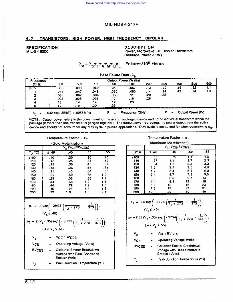
I
MIL-HDBK-217F
6.7 TRANSISTORS, HIGH POWER, HIGH FREQUENCY, BIPOLAR
SPECIFICATION DESCRIPTIONM!L-S-19500 Power, Mkrowave, RF Bipolar Transistors
(Average Power 21 W)
%= %%XAXM%ZE ‘ail”res/lo’‘O”’s
Base Failure Rate - ~.
Frequency Output Power (Watts)(GHz) 1.0 5.0 10 50 100 200 300 400 500 600I 1
s 0.5 .038 .039 .040 .050 .067 .12 .20 .36 .62 1.1.046 .047 .048 .060 .080 .14 .24 .42 .74 1.3
; .065 .067 .069 .086 .11 .20 .353 .093 .095 .098 .12 .16 .284 .13 .14 .14 .17 .235 .19 ,19 .20 .25
lb x .032 exp(.354(F) + .00558(P)) F= Frequency (GHz) p = OUtp@POwer W) INOTE: Output power refers to the power level for the overall packaged device and not to indwidual transistors within thepackage (if more than one transistor is ganged together). The output power represents the power output from the activedevice and should not account for any duty cycle in pulsed applications. Duty cycle iS accounted for when determining ‘A. I
Temperature Factor - XT(Gnlri Mdalli7atinn\\ -- !.- . . . . . . . . ..- . . . . .
Vs (VCE/BVCE@TJ (“C) s .40 .45 .50 .55sl 00 .10 .20 .30 .40110 .12 .25 .37 .49120 ,15 .30 .45 .59130 .18 .36 .54 .71140 .21 .43 .64 .85150 .25 .50 .75 1.0160 .29 .59 .88 1.2170 .34 .68 1.0 1.4180 .40 .79 1.2 1.6190 .45 .91 1.4 1.8200 .52 1.0 1.6 2.1
.1 exp((-2903 1 1
‘T =))
TJ +273 - = ‘
(VS < .40)
((
1‘T - z (VS - .35) eXP -2903 TJ ~ 273
))-m ‘
(.4 < v~ s .55)
v~ = VCE / BVCES
VCE . Operating Voftage (volts)
BVCES = Collector-Emitter BreakdownVoftage with Base Shorted toEmitter (Volts)
TJ = Peak Junction Temperature (“C)
Temperature Factor - nT/Aliiminllm Matalli7atinn\,,, ,”, ,?, .F”, ., . ..--.,,-- ., W..
Vs (VCE/BVCES)
TJ (~) s .40 .45 .50 .55Sloo .38 .75 1.1 1.5110 .57 1.1 1.7 2.3120 .84 1.7 2.5 3.3130 1.2 2.4 3.6 4.8140 1.7 3.4 5.1 6.8150 2.4 4.7 7.1 9.5160 3.3 6.5 9.7 13170 4.4 8.8 13 18180 12 18190 ?:; 15 23 $:200 30 40
((XT = .38exp -5794 1 1
))TJ +273 - = ‘
(VS s .40)
((
1 1
))nT = ?.55 (VS - .35) exp -5794 TJ + 273 - ~ ,
(.4 < Vs s .55)
v= - VCE / BVCES
VCE = Operating Voltage (Votts)
BVCES = Collector-Emitter BreakdownVoltage with Base Shorted toEmitter (Votts)
TJ = Peak Junction Temperature (“C)
6-12
Downloaded from http://www.everyspec.com
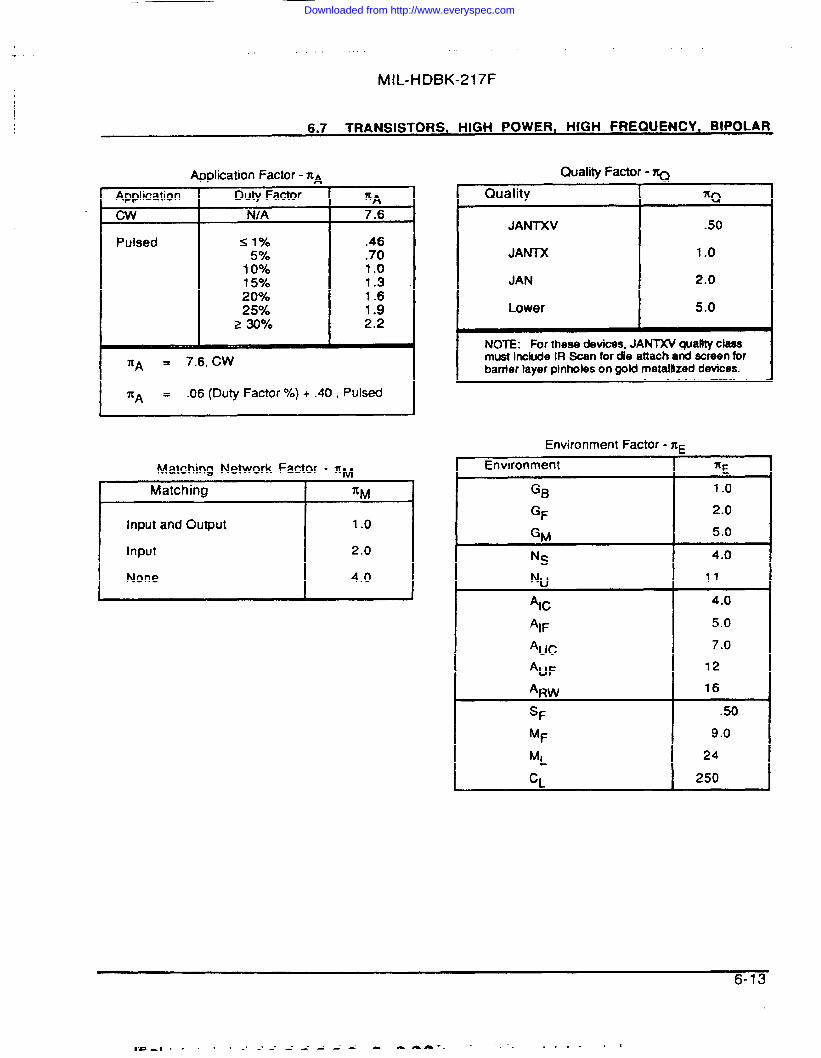
I-+
MIL-HDBK-217F
6.7 TRANSISTORS, HIGH POWER, HIGH FREQUENCY, BIPOLAR
Application
Pulsed
Application Factor - ~ADuty FactorN/A
s 1’%5!%10%+4015%20%25%2 30%
.46
.701.01.31.61.92.2
7tA = 7.6, CW
n~ = .06 (Duty Factor 0 / 0) + .40, Pulsed
Matching Network Factor - fiM
Matching ~M
Input and Output 1.0
Input 2.0
None 4.0
Quality Factor - ~—Quality ZQ
JANTXV .50
JANTX 1.0
JAN 2.0
Lower 5.0
N07E: For these devices,JANTXV qualityclassmustIncludeIR Scan for die attachand screenforbarrier layer pinholes on gold metaltized devices.
Environment Factor - zcb
Environment ~E
GB 1.0
GF 2.0
GM 5.0
Ns 4.0
Nu 11
‘Ic 4.0
‘IF 5.0
*UC 7.0
‘UF 12
*RW 16
SF .50
MF 9.0
ML 24
CL 250
6-13
m-a-l.... _._. —. -“ —. -- -- -- -- m AAM”.- .-. . . . . . I
Downloaded from http://www.everyspec.com
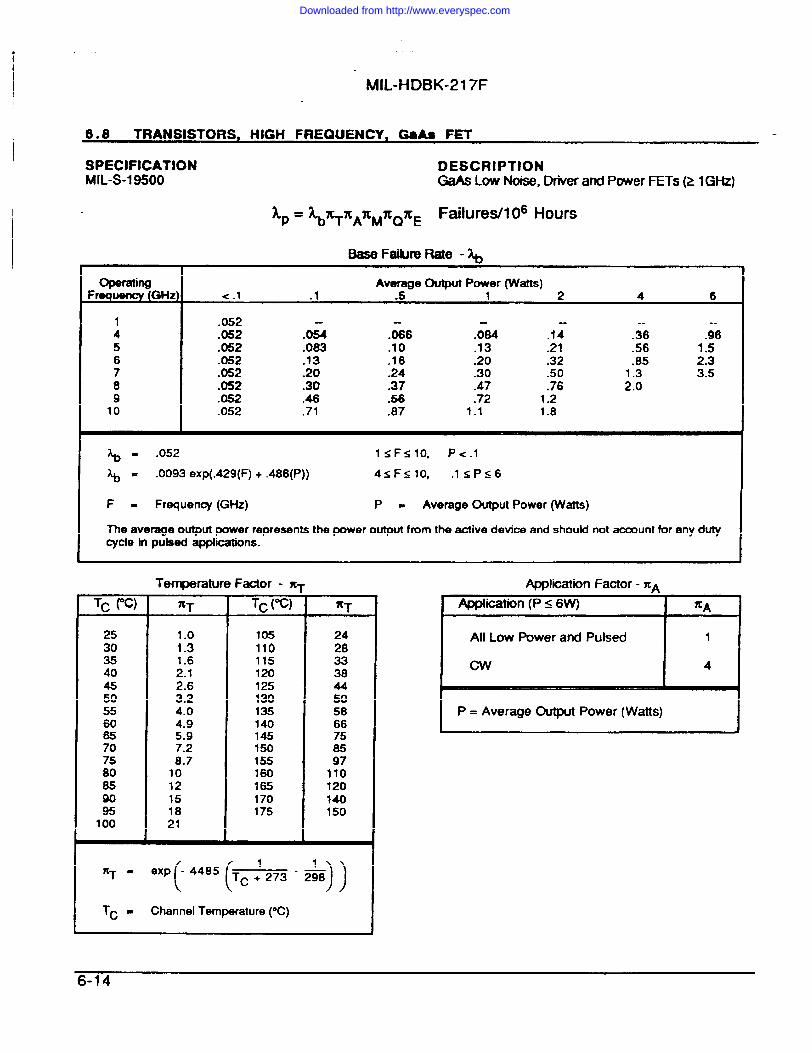
MIL4-IDBK-217F.
6.8 TRANSISTORS, HIGH FREQUENCY, GaA, FET
SPECIFICATION DESCRIPTIONMIL-S-19500
145670910
Galls Low Noke, Driver and Power FETs (2 lGHz)
Base FaihJre Rate - ~
Average Output Power (Watts)<.1 .1 .5 1 2 4 6
.052
.052
.052
.052
.052
.052
.052
.052
.054
.083
.13
.20
.30
.46
.71
.&6
.10
.16
.24
.37
::
.084
.13
.20
.30
.47
.721.1
-- -..14 .36 .96.21 .56 1.5.32 .85 2.3.50 3.5.76 ;::1.21.8
% “ .052 1< F<1o, P<.1
%= .0093 exp(.429(F) + .486(P)) 4sFs1o, .ls Ps6
F- Frequency (GHz) p. Average Output Power (Watts)
The average output power representsthe power output from the active device and should not account for any dutycycle in pulsed applications.
Tc (=)253035404550556065707s80859095100
Temperature Factor - m
1.01.31.62.1
$:;4.04.95.97.28.7101215
;7
TC (C)
M115120125130135140145150155160165170175
%T
2428333844505866
E9711012014’0150
((h - ‘Xp ‘4485 &3-L 298))
Application Factor - XAApplication (Ps 6W) I ~A
All Low Power and Pulsed 1
4
P = Average Output Power (Watts)
TC = Channel Temperature (“C)
U-14
Downloaded from http://www.everyspec.com
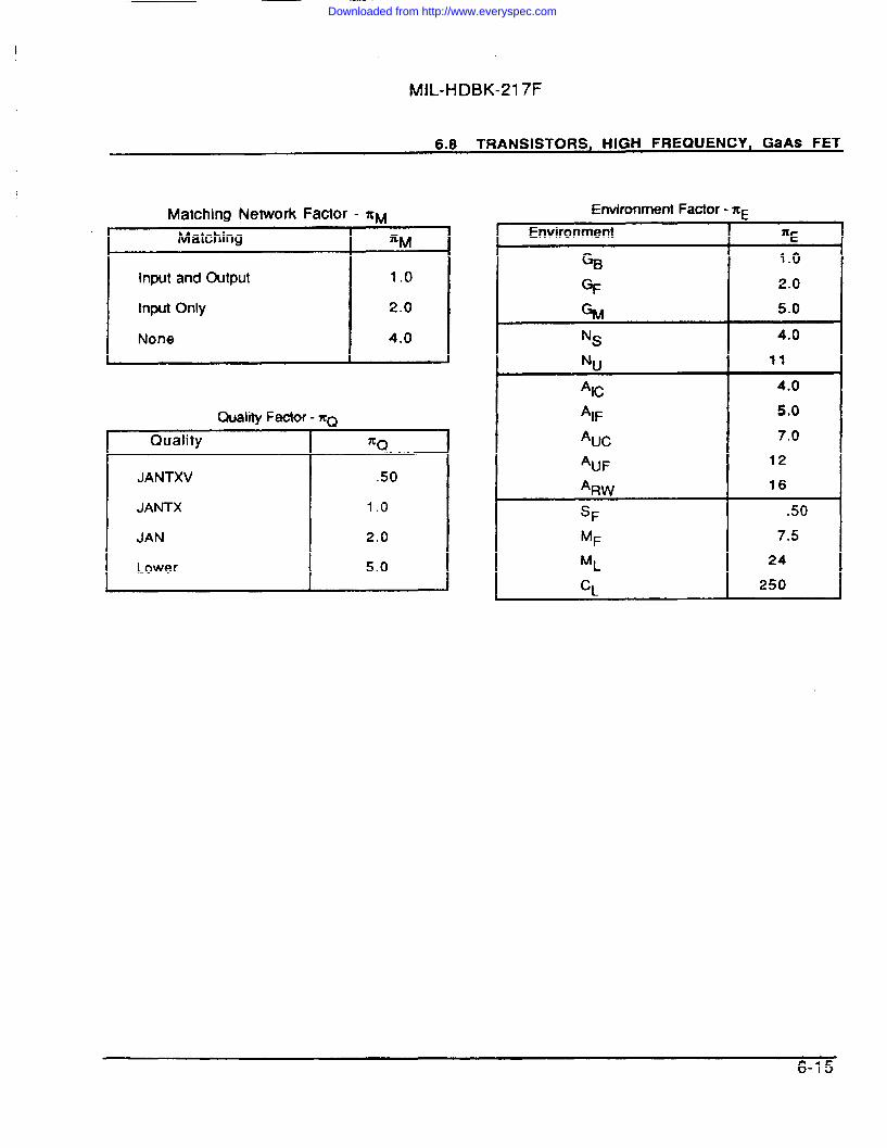
MIL-HDBK-217F
6.8 TRANSISTORS, HIGH FREQUENCY, GaAs FET
Matching Network Factor - ~M
Matching ~M
Input and Output 1.0
Input Only 2.0
None 4.0
Qualiiy Factor- ICQ
Quality ~ Q
JANTXV .50
JANTX 1.0
JAN 2.0
Lower 5.0
Environment Factor - xcL
Environment [ ~E
%3 1.0
GF 2.0
% 5.0
NS 4.0
N“ 11
%c 4.0
% 5.0
*UC 7.0
*UF 12
‘RW 16
SF .50
MF 7.5
ML 24
CL 250
Downloaded from http://www.everyspec.com
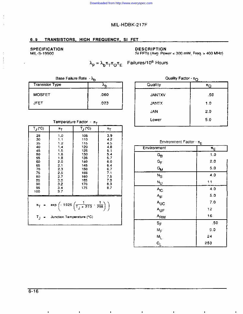
MIL-HDBK-217F
6.9 TRANSISTORS, HIGH FREQUENCY, Si FET
SPECIFICATIONMIL-S-19500
~ = &Tz@E
Base Failure Rate - ~Transistor Type A~
I MOSFETI
.060
I JFET I .023
TJ (“C)
253035404550556065707580859095100
Temperature Factor - m
XT
1.01.11.21.41.51.61.82.02.12.32.52.73.03.23.43.7
105110115120125130135140145150155160165170175
7tT
3.94.24.54.85.15.45.76.06.46.77.17.57.98.38.7
((- 1925 1 1‘T = exp TJ + 273 -E
))
TJ = Junction Temperature (“C)
DESCRIPTIONSi FETs (Avg. Power< 300 mW, Freq. >400 MHz)
Failures/l OGHours
Quality Factor - ~
Quality
JANTXV
JANTX
JAN
Lower
.50
1.0
2.0
5.0
Environment Factor - ~=L
Environment I xc I
GB
GF
GM
N~
N“
AIC
‘IF
‘Uc
*UF
‘RWSF
MF
ML
CL
1.0
2.0
5.0
4.0
11
4.0
5.0
7.0
12
16
.50
9.0
24
250
6-16
Downloaded from http://www.everyspec.com
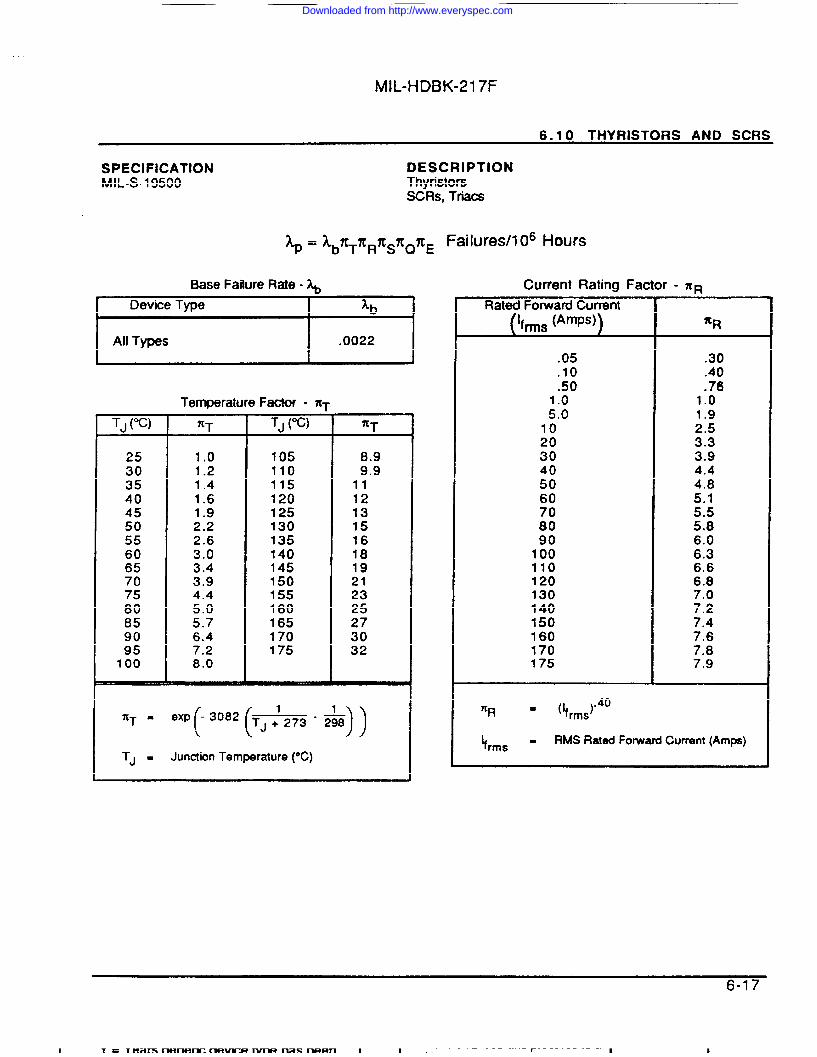
MIL-HDBK-217F
6.10 THYRISTORS AND SCRS
SPECIFICATION DESCRIPTIONMIL-S-19500 Thyristors
SCRS, Triacs
Base Failure Rate - ~
I Device Type I Lb I
I All TypesI
.0022I
TJ (%)
253035404550556065707580859095100
Temperature Factor - q
1.01.21.41.61.92.22.63.0
:::4.45.05.76.47.28.0
TJ(%) -
105110115120125130135140145150155160165170175
8.99.91112131516la19212325273032
((-3082 1 1~T = exp TJ + 273))
-m
TJ = Junction Temperature (“C)
Failures/l 06 Hours
Rated Forward Current‘ffms (Amps)
Current Rating Factor - ~R
.05,10.501.05.0102030405060708090100110120130140150160170175
.30
.40
.761.01.92.53.33.94.44.85.15.55.86.06.36.66.87.07.27.47.67.87,9
m = ($rmJ”40
+ RMS Rated ForwardCurrent (Amps)rms =
6-17
Downloaded from http://www.everyspec.com
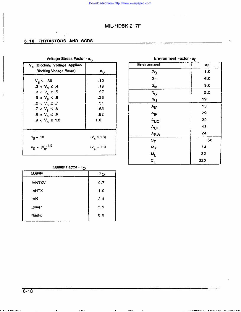
MIL-HDBK-217F.
. .
6.10 THYRISTOf?S AND SCRS —
Voltage Stress Factor - XCw
V~ (Blocking Voltage Applied/BlockingVottage Rated) Xs
v~ s .30 .10.3<v #.4 .18.4<v #.5 .27.5< V#.6 .38.6< V#.7 .51.7< [email protected] .65.8< V~S.9 .82.9 < v~ s 1.0 1.0
7CSD.1O (VSs 0.3)
~s = (Vs)1.9 (VS> 0.3)
Quality Factor - ZQQuality ! ZQ
JANTXV 0.7
JANTX 1.0
JAN 2.4
Lower 5.5
Plastic 8.0
Environment Factor - XCL
Environment %E
% 1.0
GF 6.0
% 9.0
NS 9.0
NU 19
Alc 13
‘IF 29
‘Uc 20
‘UF 43
%J 24
SF .50
MF 14
ML 32
cL 320
6-18
Downloaded from http://www.everyspec.com
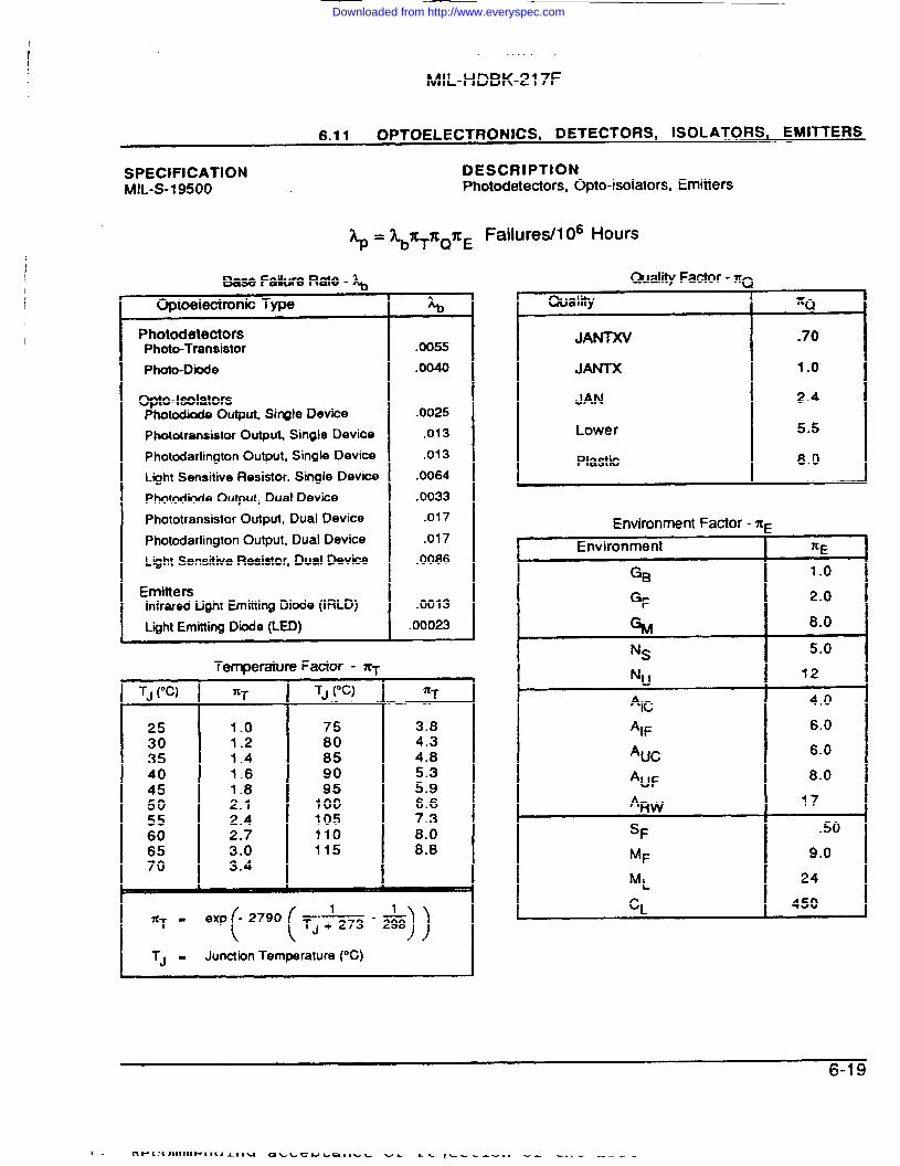
. .
MIL-HD6K-217F
6.11 OPTOELECTRONICS, DETECTORS, ISOLATORS, EMITTERS
SPECIFICATION DESCRIPTIONMIL-S-19500 Photodetectors, Opto-isolators, Emitters
Base Faiture Rate - &
OptoelectfonkType - %PhotodetectorsPhoto-Transistor .0055Photo-Diode .0040
Opto-isolatorsPhotodbde Output, Si@e Device .0025
Photot:aosistor Output, Single Device .013
Photodarlington Output, Single Device ,013
Light Sensitive Resistor, Single Devioe .0064
Photodiode Output, Dual Device .0033
Phototransistor Output, Dual Device .017
Photodarlington Output, Dual Device .017
Lght Sensitive Resistor, Dual Device .0086
EmittersInfrared Light Emitting Diode (IRLD) .0013LightEmittingDiode (LED) .00023
Temperature Factor - ~T
TJ (“C) XT TJ (“C) XT
25 1.0 75 3.830 1.2 80 4.335 1.4 85 4.840 1.6 90 5.345 1.8 95 5.950 2.1 100 6.655 2.4 105 7.360 2.7 110 8.065 3.0 115 8.870 3.4
((-2790 1 1ttT = exp TJ +273-~
))TJ = Junction Temperature (“C)
Failures/l 06 Hours
Quality Factor - ZQQuality YCQ
JAW .70
JANTX 1.0
JAN 2.4
Lower 5.5
Plastic 8.0
Environment Factor - nEnvironment
GB
GF
GMNs
N I
‘Ic
‘IF
‘Uc
‘UF
‘RWSF
MF
ML
c1
~E
1.0
2.0
8.0
5.0
12
4.0
6.0
6.0
8.0
17
.50
9,0
24 ;
450 I
<
6-19
Downloaded from http://www.everyspec.com
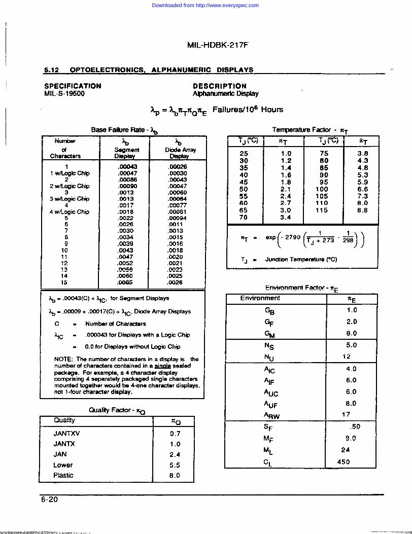
I
MIL-HDBK-217F
I 6.12 OPTOELECTRONICS, ALPHANUMERIC DISPLAYS —
SPECIFICATION DESCRIPTIONMIL-S-19500 ~numedc Display
.
Base FaihJre Rate - &
% “ &T’QzE Failures/l 06 Hours
Number % “+)d
Charactws1 .00043 .00026
1whgk Chip .00047 .000302 .00066 X)0043
2 W/b@C Chip .00090 .000473 .0013 .00060
3 Wlhxjo chip .0013 .000644 .0017 .00077
4 w/Logic Chip .0018 .000815 .0022 .000946 .0026 .00117 .0030 .00138 .0034 .00159 .0039 .001610 .0043 .0018
.0047 .0020:; .0052 .002113 .0056 .002314 .0060 .002515 .0065 .0026
~ - .00043(C)+ ~C, for Segment Displays
~. .00009+ .00017(C)+ ~C, Diode Array Displays
c= Number of CharaAers
%- .000043 for Displays with a Logic Chip
- 0.0 for Displays without Imgic Chip
NOTE: The numbar of characters in a display is thenumber of characters mntained in a _ sealedpackage. For example, a 4 character displaycomprising 4 separately packaged single charactersmounted together would be tine character dispiays,not 1-four character display.
I Quality
JANTXVJANTX
JAN
LowerPlastic
Quality Factor - ~lcQ
0.71.0
2.45.58.0
TJ (“C)
25303540455055606570
Tenqwature Factor - q
~T TJ (%) %T
1.0 75 3.81.2 80 4.31.4 85 4.81.6 90 5.31.8 95 5.92.1 100 6.62.4 105 7.32.7 110 8.03.0 115 8.83.4
((-2790 1 1%T = exp TJ + 273))
-ZE
TJ = Junction Temperature ~C)
Environment Factor - xcEnvironment
%Ns
Nu
AC
‘IF
%c
*UF
MF
ML
Ci
1.0
2.0
8.0
5.0
12
4.0
6.0
6.0
8.0
17
.50
9.0
24
450
6-20
---- ------ --------
Downloaded from http://www.everyspec.com
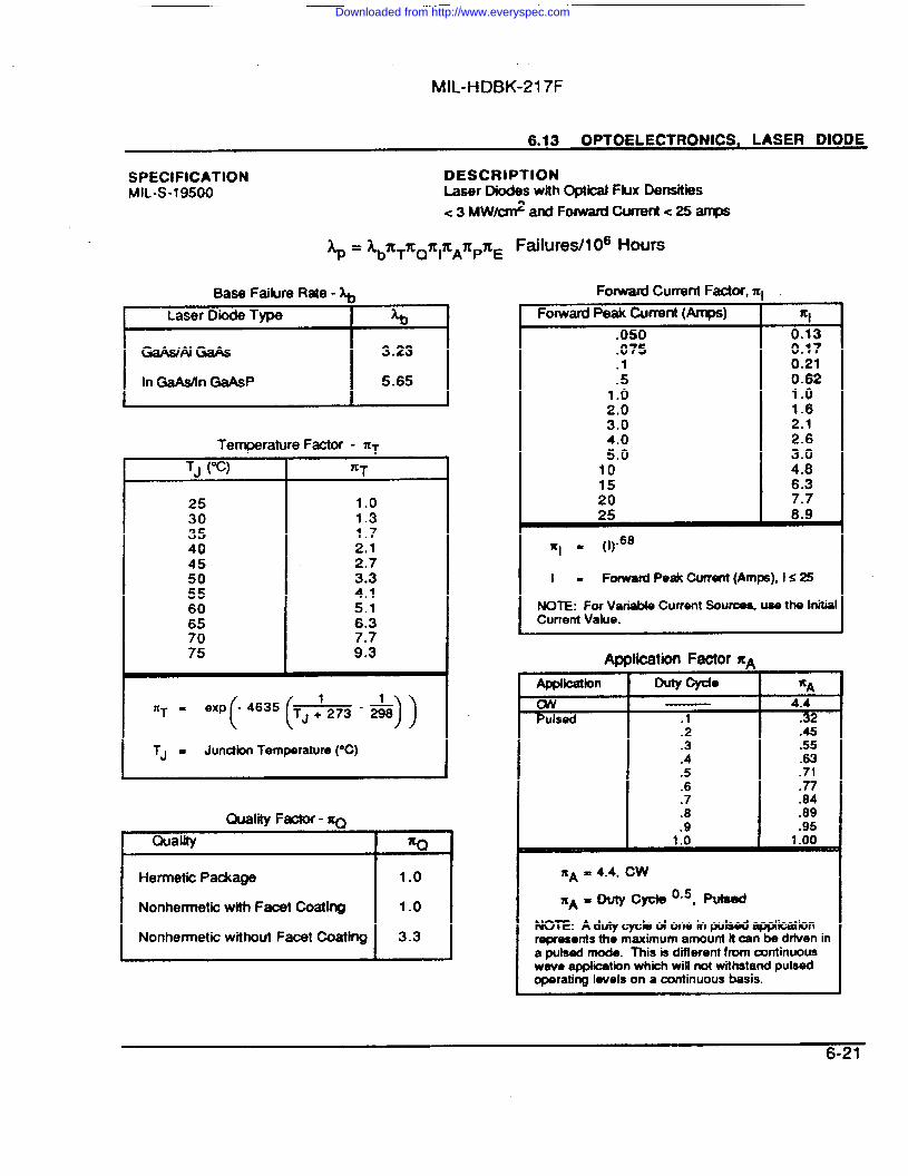
—
MIL-HDBK-217F
6.13 OPTOELECTRONICS, LASER DIODE
SPECIFICATION DESCRIPTIONMIL-S-19500 laser Diodes with Optical Flux Densities
<3 MW/cr# amt Fofward Cufrmt <25 ~
Temperature Factor - XTTJ (“C)
2530354045505560657075
1.01.31.72.12.73.34.15.16.37.79.3
(( 1 1XT = exp -4635 TJ + 273 - ~
))
TJ = JunctionTemperature(“C)
Quality Factor - ~Quality 1-
Hermetic Package 1.0
Nonhermetic with Faoet Coating 1.0
Nonhermetic without Facet Coating 3.3
Failures/l 06 Hours
Forward Cument Factor, IForward Peak Current (Anps)
.050
.075
.1
.51.02.03.04.05.0101520
q~
0.170.210.621.01.62.12.63.04.86.37.78.9
q - (1)”68I - FonnmrdPeak Currant(Amps), I $25
NOTE: For VariaMa Current Souroes, use the InitialCurrent Value.
Application Factor %A
Application Duty Cydo x~4.4
Pulsed 1 .1 .32.2.3.4
::.7.8.9
.45
.55
.63
.71
.77
.84
.89
.95
~A = 4.4, CW
%A = ~ Cycle 0-5,f%.i-d
NOTE: A duty cyclaof one in pulsed applicationrepresents the maximum amount it can ba driven ina pulsad mode. This is different from wntinuouswave applicationwhichwillnotwithstandpulsedoparatingIavelson a continuousbasis.
-.. 2 ----- --———— ——4
Downloaded from http://www.everyspec.com
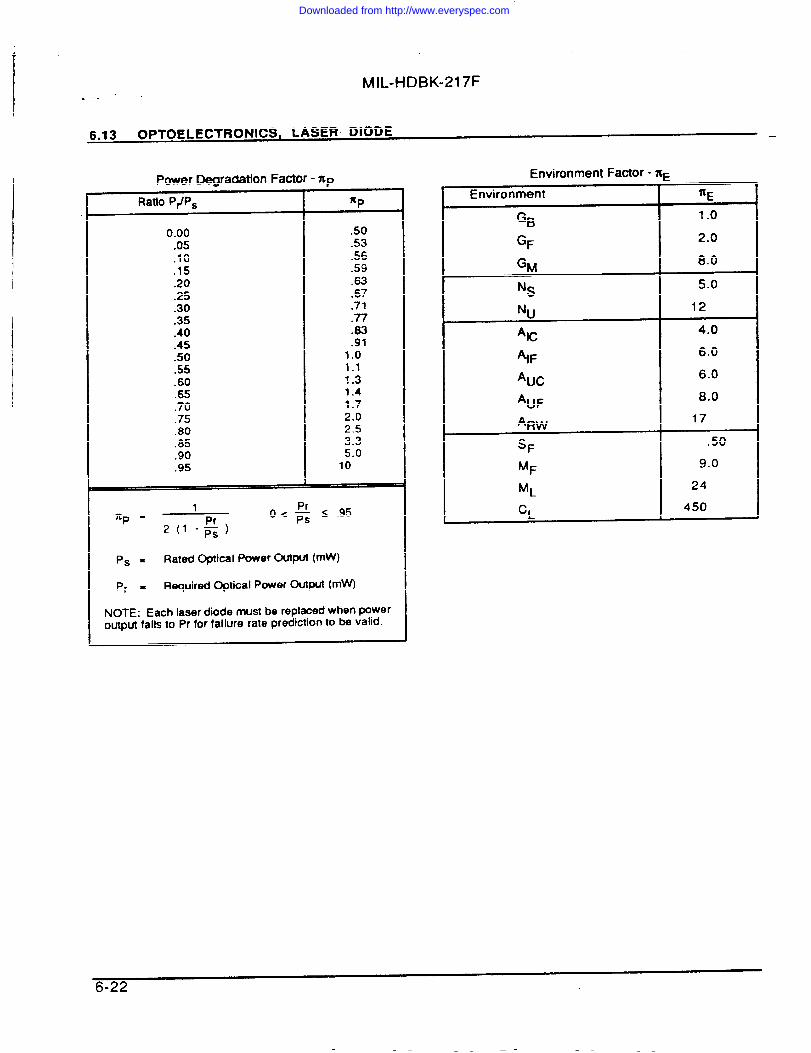
IJ
. . .
MIL-HDBK-217F
6.13 OPTOELECTRONICS, LASER DIODE —
Power ~radation Factor - np
Ratio P~P~ I %p#
0.00 .50.05 .53.10 ,56.15 .59.20 .63.25 .67.30 .71.35 .77.40 .83.45 .91.50 1.0.55 1.1.60 1.3.65 1.4.70 1.7.75 2.0.80 2.5.85 3.3.90 5.0.95 10
~
1lcp = ~ s .95“PS
2 (1 -&
Ps = Rated Optical Power Output (rnW)
Pr = Required Optical Power Output (mW)
NOTE: Each laser diode must be replaced when poweroutput falls to Pr for fai lure rate prediction to be valid.
Environment Factor - fiE 9
I Environment [ ttE 1
I GB
GFI 1.0
I 2.0
GM 8.0
Ns 5.0
Nu 12
Ac 4.0
‘IF
%c
‘UF
‘RWSF
MF
ML
6.0
6.0
8.0
17
.50
9.0
24
450
6-22
Downloaded from http://www.everyspec.com
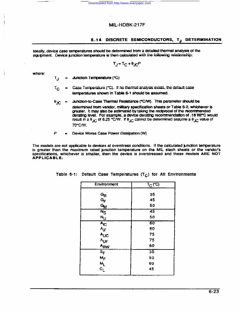
MIL-HDBK-217F
6.14 DISCRETE SEMICONDUCTORS, TJ DETERMINATION
Idealty, device case temperatures should be detetined from a detailed thermal anatysis of theWl@me~. D8Vb #.IndOn te~-m iS then ~M~ with tb folbwing relationship:
where:TJ =
TC =
P=
TJ = Tc + e~p
Junction Temperature(%)
Case Temperature (~). tf no thermal analysis exists, the defautt casetemperatures shown in Table ~1 should be assumed.
Junction-to-Case Thermal Resistance (“CAN). This parameter should bedetermhwd from vendor, military specffkation sheets or Table 6-2, whiohever isgreater. It may also be estimated by taking the mclpmcal of the reconvnended&wa!lng Ieve!. For examp!e, a devtce derating reconxnendatton of .16 W“ wou!drestAina6K of6.250CAN. lf6wcannot bedetermhwd assurnea O~vabeof7o”c/w.
Device Worse Case Power Diss@ation (W)
The models are not applicable to devices at overstress conditions. If the calculated junction temperatureis greater than the maximum rated junction temperature on the MIL slash sheets or the vendor’sspecifications, whichever is smaller, then the device is overstressed and these models ARE NOTAPPLICABLE.
Table 6-1: Default Caee Temperatures (Tc) for All Environments
Environment TC (“C)
I I 3545
% 50Ns 45Nu 50AC 60
‘IF 60
‘Uc 75
‘UF 75
*RW 60SF 35MF 50ML 60CL 45
Downloaded from http://www.everyspec.com
MIL-HDBK-217F
6.14 DISCRETE SEMICONDUCTORS, T i DETERMINATION —
Table 6-2: Approximate Juriction-to-Case Thermal Resistance (6JC) for SemiconductorDevices In Varfous Package Sizes”
Package Type OJC (“w Package Type Ok (%A#)
TO-1 70 TO-205AD 70TO-3 10 TO-205AF 70TO-5 70 TO-220 5TO-8 70 5TO-9 70 Do-5 5TO-12 70 D07 10TO-1 8 70 5TO-28 5 Do-9 5TO-33 70 DO-13 10TO-39 70 DO-14 5T041 10 Do-29 10TO-44 70 Do-35 10T046 70 DO-41 10TO-52 70 DO-45 5TO-53 5 DO-204MB 70TO-57 5 DO-205AB 5TO-59 5 PA-42A,B 70TO-60 5 PD-36C 70TO-61 5 PD-50 70TO-63 5 PD-77 70To-66 10 PD-180 70TO-71 70 PD-319 70TO-72 70 PD-262 70TO-83 5 PD-975 70TO-89 22 PD-280 70TO-92 70 PD-216 70TO-94 5 PT-2G 70TO-99 70 PT-6B 70TO-126 PH-13 70TO-127 : PH-16 70TO-204 10 PH-56 70TO-204AA 10 PY-58 70
PY-373 70
“When available, estimates must be based on military specification sheet or vendor vaiues, whichever OJC
is higher.
6-24
Downloaded from http://www.everyspec.com
MIL-HDBK-217F
6.15 DISCRETE SEMICONDUCTORS, EXAMPLE
Example
Given: Silicon dual transistor (complementary), JAN grade, rated for 0.25 W at 25”C, one sideonty, and 0.35 W at 25”C, both sides, with TM = 2000C, operating in linear service at55°C case temperature in a sheltered naval environment. Side one, NPN, operating at0.1 W and 50 percent of rated voltage and side two, PNP, operating at 0.05 W and 30percent of rated voltage. The device operates at iess than 200 MHz.
Since the device is a bipolar dual transistor operating at low frequency (c200 Miiz), it falls into theTransistor, Low Frequency, Bipoiar Grwp and the appropriate modei is given in %ction 6.3. Since thedevice is a dual device, it is necessary to compute the faiiure rate of each side separately and sum themt~e{k. Also, si~ OJc k uf’k~wn, OJc = 70%/w ~i~ be a~md.
Based on the given information, the following model factors are determined from the appropriate tablesshown in Section 6.3.
.000742.2 s@O1, TJ=TC+eJC %55+70( .1).62°c2.1 Side 2, TJ = 55+ 70(.05) = 59°C1.5.68 Using equation shown with XR tabie, Pr = .35 W.21 Side 1, 5070 Voltage Stress.11 Side 2, 3(I?%Voitage Stress2.49
$ = (.00074)(2.2)(1 .5)(.68) (.21)(2.4)(9) + (.00074)(2.1)(1 .5)(.68) (.1 1)(2.4)(9)
= .011 Faiiures/106 Hours
6-25
Downloaded from http://www.everyspec.com
MIL-HDBK-217F
7.1 TUBES, ALL TYPES EXCEPT TWT AND MAGNETRON
DESCRIPTIONAll Types Except Traveling Wave Tubes and Magnetrons.Includes Receivers, CRT, Thyratron, Crossed Field Amplifier,Pulsed Gridded, Transmitting, Vidicons, Twystron, PulsedKlystron, CW Klystron “
~ = kb7cLnE Failures/l 06 Hours
Base Failure Rate - ~
I
(Includes Both Rando[Tube Type Lb
ReceiverTnode, Tetrode, Pentode 5.0Power Rectifier 10
ThyratronCrossed Field AmplifierQK681
50
260SFD261 150
Pulsed Gridded2041 1406952 390
TransmittingTriode, Peak Pwr. s 200 KW, Avg. 75Pwr, s 2KW, Freq. g 200 MHz
Tetrode & Pentode, Peak Pwr. 100s 200 KW, Avg. Power 5 2KW,Freq. S 200 KWIf any of the above limits exceeded 250
VidiconAntimony Trisulfide (Sb2S3)Photoconductive Material 51
Silicon Diode Array PhotoconductiveMaterial 48
TwystronVA144 850VA145E 450VA145H 490VA913A
Klystron, Pulsed”4KMP1OOOOLF8568L3035L3250L3403SAC42AVA842Z501OAZM3038A
230
4323066699310018
150190
● If the pulsed Klystron of interest is not listed above,use the Alternate Pulsed Klystron Ab Table onthe following page.
and Wearout Failures)Tube Type
Klystron, Low Power,(e.a Local Oscillator)
Klystron, Continuous Wave*3K3000LQ3K50000LF3K21OOOOLQ3KM300LA3KM3000LA3KM50000PA3KM50000PA13KM50000PA24K3CC4K3SK4K50000LQ4KM50LB4KM50LC4KM50SJ4KM50SK4KM3000LR4KM50000LCI4KM50000LR4KM170000LA882488258826VA800EVA853VA856BVA888E
30
9.054
1506419110120150610293028153837140795715
1301202807022065
230
● If the CW Klystron of interest is not listed above,use the Alternate CW Klystron ~ Table on thefollowing page.
Downloaded from http://www.everyspec.com
MIL-I-IDBK-217F
7.1 TUBES, ALL TYPES EXCEPT TWT AND MAGNETRON —
Attemate* Base Failure Rate for Pulsed Klystrons - A
Zs!&!L.01.30.801.03.05.08.01025
F(GHz).2 .4 .6 .8 1.0 2.0 4.0 6.0
16 16 16 16 16 1616 16 17 17 17 18 ;: ;:16 17 17 18 18 21 25 3017 17 18 18 19 22 28 3418 20 21 23 25 34 5119 22 25 28 31 45 7521 25 30 35 40 63 11022 28 34 40 45 7531 45 60 75 90 160
+2= 2.94 (F)(P) + 16
F = Operating Frequency in GHz, 0.2s Fs 6P- Peak Output Power in MW, .01 s Ps 25 and
P s 490 F-295
“See previous page for other Klystron Base FailureRates.
Aftemate” Base Failure Rate for CW Klystrons - ~
3K!!!!L0.1
;;;5.08.010305080100
30 31 33 34 38 47 57 6631 32 33 34 39 48 57 6632 33 34 35 40 49 5833 34 35 36 41 5034 35 37 38 4235 36 38 39 4345 46 48 4955 56 58 5970 71 7380 81
%“ 0.5P + .00046F + 29
P= Average Output Power in KW, 0.1 s Ps 100and Ps 8.0(10) 6(F)-1”7
F = Operating Frequency in MHz,300s Fs8000
●See previous page for other Klystron Base FailureRates.
Learning Factor - XI
T (years) ‘LI
<1 10
2 2.3
>3 1.0
q = 10(T) -2”’, 1 sT<3= 10, TsI= 1,T23
T = Numtw of Years since Introductionto Field Use
Environment
GB
GF
GM
Environment Factor - nE
T
N~
Nu
%c
‘IF
%c
‘UF
‘RWSF
MF
ML
CL
1.0
14
8.0
24
5.0
8.0
6.0
12
40
.20
22
57
1000
Downloaded from http://www.everyspec.com
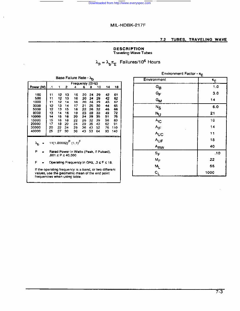
MIL-HDBK-217F
7.2 TUBES, TRAVELING WAVE
DESCRIPTIONTraveling Wave Tubes
Xp = &E Failures/l 06 Hours
Environment Factor - XFBase Failure Rate - &
Frequency (G-Hz)Power (W) .1 1 2 4 6 8 10 14 18
100 11 12 13 16 20 24 29 42 61500 11 12 13 16 20 24 29 42 621000 11 12 14 16 20 24 29 43 623000 12 13 14 1721253044655000 12 13 15 18 22 26 32 46 688000 13 14 16 19 23 20 33 49 7210000 14~5~62024293551 7515000 15 16 18 22 26 32 39 56 8320000 17 18 20 24 29 35 43 62 9130000 20 22 24 29 36 43 52 76 11040000 25 27 30 36 43 53 64 93 140
%= 11(1.00002)P (1.l)F
p. Rated Power in Watts (Peak, if Pulsed),.001< P s 40,000
F = Operating Frequency in GHz, .3s Fs 18.
If the operating frequency is a band, or two differentvalues, use the geometric mean of the end pointfrequencies when using table.
Environment ~E
GB 1.0
GF 3.0
GM 14
Ns 6.0
N“ 21
%c 10
‘IF 14
‘Uc 11
‘UF 18
‘RW 40
SF .10
MF 22
ML 66
CL 1000
/-3
Downloaded from http://www.everyspec.com
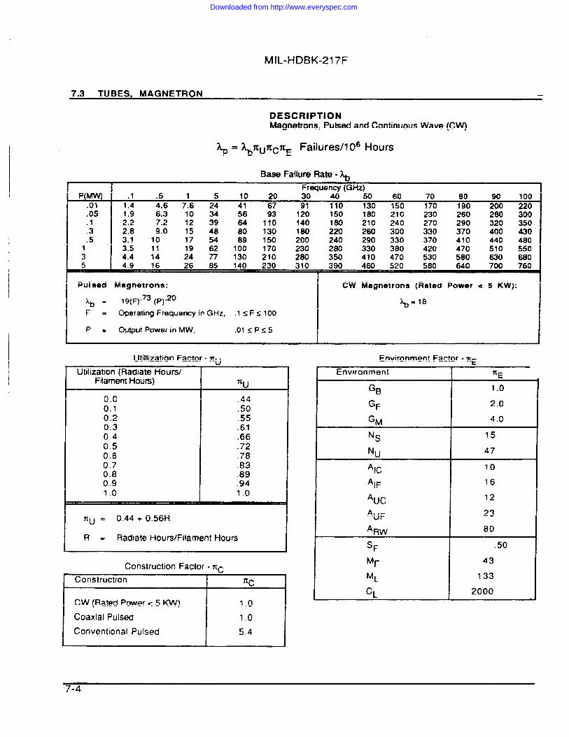
MIL-HDBK-217F
7.3 TUBES, MAGNETRON —
DESCRIPTIONMagnetrons, Pulsed and Continuous Wave (CW)
%=% 7c@@E Failures/l 06 Hours
Base Failure Rate - ~
Qs!!?!m.01.05.1.3.513
Frequency (GHz).1 .5 1 5 10 20 30 40 50 60 70 80 90 1001.4 4.6 7.6 24 41 67 91 110 130 150 170 190 200 2201.9 6.3 10 34 56 93 120 150 180 210 230 260 280 3002.2 7.2 12 39 64 110 140 180 210 240 270 290 320 3502.8 9.0 15 48 80 130 180 220 260 300 330 370 400 4303.1 10 17 54 89 150 200 240 290 330 370 410 440 4803.5 11 19 62 100 170 230 280 330 380 420 470 510 5504.4 14 24 77 130 210 280 350 410 470 530 580 630 680
Pulsed Magnetrons: I CW Magnetrons (Rated Power < 5 KW):
%) = ‘9(F).73 ~pl.20 I A@8F = Operating Frequency in GHz, .1 s Fs 100
P = Output Power in MW, .ol<p~5 IUtilization Factor - q I Environment Factor - mr
Utilization (Radiate Hours/FilamentHours) 7CU
0.0 .440.1 .500.2 .550.3 .610.4 .660.5 .720.6 .780.7 .830.8 .890!9 .941.0 1.0
nu = 0.44 + 0.56R
R = Radiate Hours/Filament Hours
Construction Factor - mu
Construction XC
CW (Rated Power< 5 KW) 1.0
Coaxial Pulsed 1.0Conventional Pulsed 5.4
Environment 1 nc
GB 1.0
GF 2.0
GM 4.0
N~
Nu
*IC
‘IF
*UC
‘UF
*RW
MF
ML
c,
15
47
10
16
12
23
80
.50
43
133
2000
/-4
Downloaded from http://www.everyspec.com
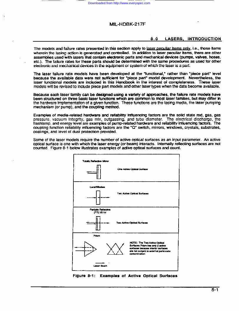
MIL-HDBK-217F
8.0 LASERS, INTRODUCTION
The models and failure rates presented in thk section apply to ~. . , i.e., those items
wherein the Iasing action is generated and controlled. In addition to laser peculiar Items, there are otherassernbhes used with lasers that contain electronic parts and mechanical devices (pumps, valves, hoses,etc.). The failure rates for these parts should be determined with the same procedures as used for otherelectronic and mechanid devices in the equipment or system of which the laser is a part.
The laser failure rate models have been developed at the “functional,” rather than ‘piece part” levelbecause the available data were not sufficient for “piece part” model devebpment. Nevertheless, thelaser functional models are included in this Handbook in the interest of completeness. These lasermodels will be revised to include piece part modek and other laser types when the data become available.
Because each laser family can be designed using a variety of approaches, the failure rate rnodets havebeen structured on three basic laser functbns whii are common to most laser families, but may differ inthe hardware knplernentation of a given function. These functions are the Iasing rneda, the laser pumpingmechanism (or pump), and the coupfing method.
Examptes of media-related hardware and reliability Influencing factors are the solid state rod, gas, gaspressure, vacuum integrity, gas mix, outgassing, and tube diameter. me electrical discharge, theflashlamp, and energy level are exarr@es of pump-related hardware and reliabilii influencing factors. Thecoupling function reliability influencing factors are the “Q” switch, mirrors, windows, crystals, substrates,coatings, and level of dust protection provided.
Some of the laser models require the number of active optical surfaces as an input parameter. An activeopticai surface is one with which the laser energy (or beam) interacts. internally reflecting surfaces are notcounted. Figure 8-1 below illustrates examples of active optiil suffaces and count.
Tot* wloclw9 Mnuf
+
cho ActhmQxkalsurb20
Pdult
—.b@u *am
Figure 8-1: Examples of Active Optical Surfaces
8-1
Downloaded from http://www.everyspec.com
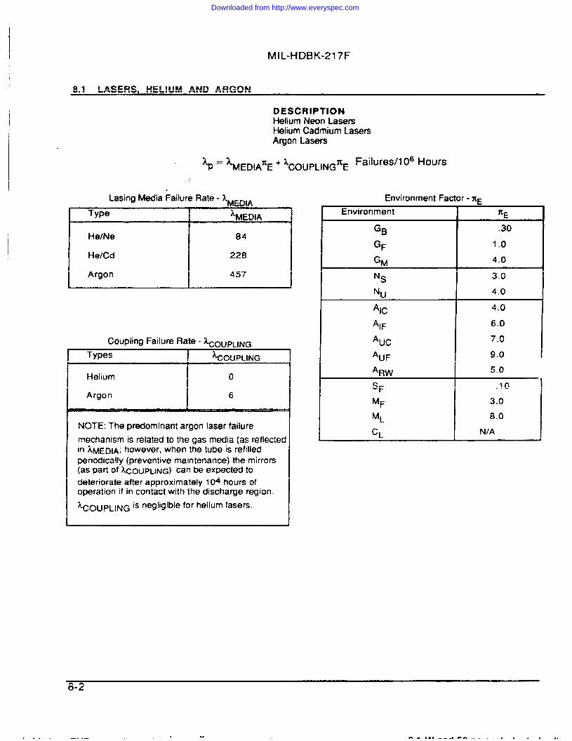
I
MIL-HDBK-217F
8.1 LASERS, HELIUM AND ARGON
DESCRIPTIONHelium Neon LasersHelium Cadmium LasersArgon Lasers
n Failures/l 06 Hours~ = ‘MED,AZE + ‘COUPLING E.. “
Lasing Media Failure Rate - kMEDIA
Type ‘MEDIA
He/Ne
He/Cd
Argon
84
228
457
Coupling Failure Rate - ~0[ lpi ,NG----- ...—Types %OUpLING
Helium 0
Argon 6
NOTE: The predominant argon laser failure
mechanism is related to the gas media (as reflectedin XMEDIA; however, when the tube is refilledperiodically (preventive maintenance) the mirrors(as part of ~OUpLIN@ can be expected todeteriorate after approximately 104 hours ofoperation if in contact with the discharge region.
‘COUPLING is negligible for helium lasers.
Environment Factor - n=b
Environment ~E
GB .30
GF 1.0
GM 4.0
N~ 3.0
Nu 4.0
%c 4.0
% 6.0
‘Uc 7.0
‘UF 9.0
‘RW 5.0
SF .10
MF 3.0
ML 8.0
CL NIA
8-2
Downloaded from http://www.everyspec.com
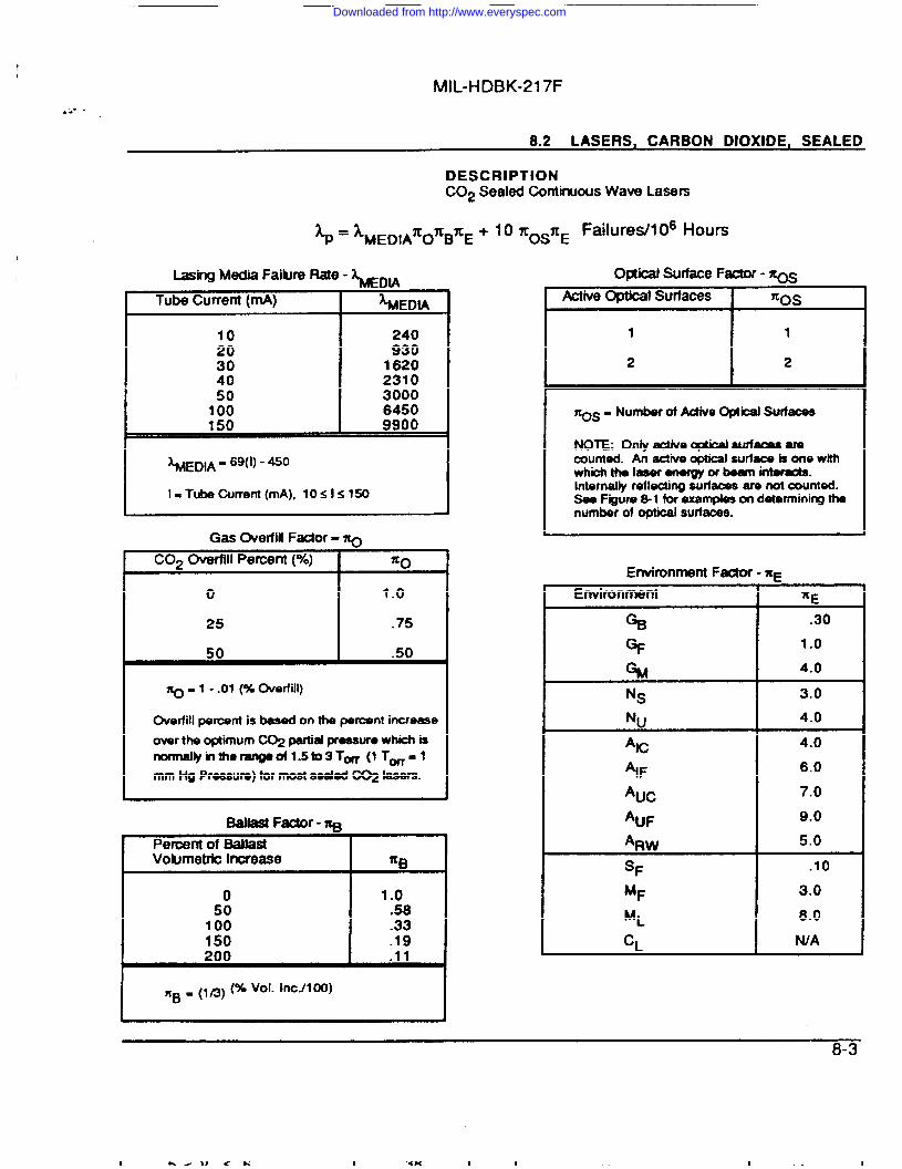
●-” “
MIL-HDBK-217F
8.2 LASERS, CARBON DIOXIDE, SEALED
DESCRIPTIONC02 Sealed Continuous Wave Lasers
Lasing Media FaiWe Rale - ~DM
Tube Current (rnA) I %UEDIA
1020304050100
240930
1620231030006450
%tEDIA - 69(1)-‘0
l= Ttitimti(mA), 10s Is15O
Gas Overfill Factor = *C02 Overfill Percent (%)
o
25
50
%0
1.0
.75
.50
%-1 -.01 (%0Overfill)
Overfillpercent is based on the psrwnt increaseovsr the o@imum002 partialpssure which isnormalIyintherango ofl.5t03Tm (llm=lmmHg Prassure)formostsealad C02 lasers.
Peroent of BaJlastVohmetric Increase
o50100150200
1.0.58.33.19.11
n~ - (1~) (% Vol. Inc./l 00)
-.Active OptW Surfaces ‘0s
1 1
2 2
~S - Numbr of Active Optical SUrfaces
NOTE: Only *ive optical surfaoss arscounted. An active optical surfaca is one withwhiohth.laser anorgyorbwn~Internallyreflecting surfaces are not oounted.Sae Fquro 8-1 for exampleson datorminingthenumber of optical surfaces.
Environment Faotor - XEEnvironment %E
%3 .30
% 1.0
GM 4.0
Ns 3.0
Nu 4.0
AC 4.0
‘IF 6.0
*UC 7.0
*UF 9.0
‘RW 5.0
sF .10
hu~ 3.0
ML 8.0
c’ WA
U-3
Downloaded from http://www.everyspec.com
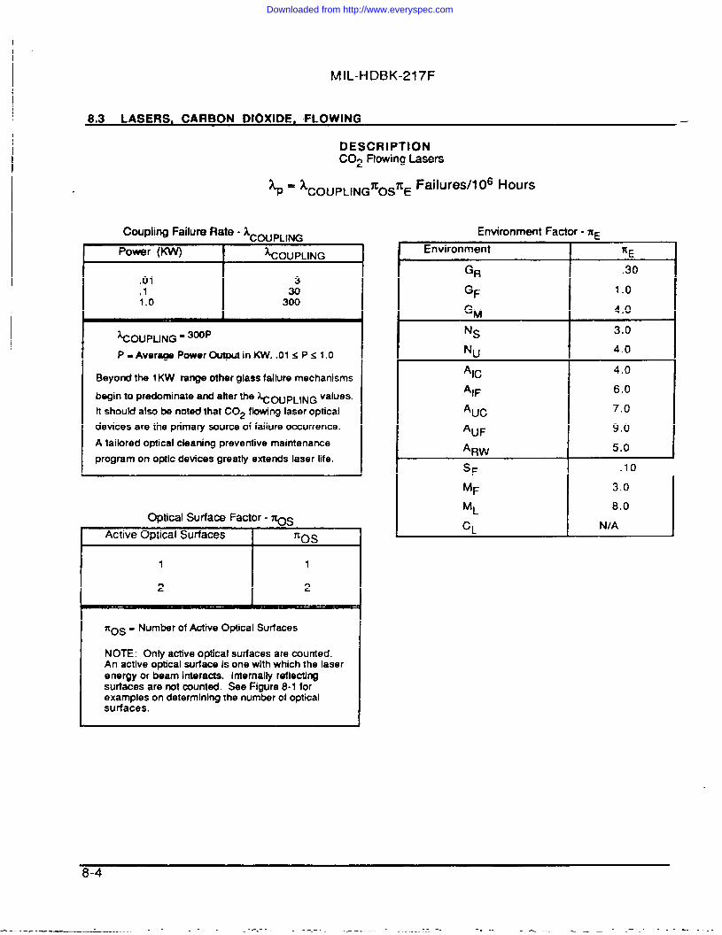
MIL-HDBK-217F
8.3 LASERS, CARBON DIOXIDE, FLOWING —
DESCRIPTIONC02 Flowing Lasers
x Failures/l OGHours+J = &JpLIN&OS E
Coupling Failure Rate - XCWPL,NG
Power (KW) I %OUpLING
.01
.1 I 21.0 300
%OUPUNG” 3WPP _ Aver- PowerOutputin KW, .01 s Ps 1.0
Beyond the 1KW range other glass failure mechanisms
b~in to predominate and alter the ~OUpLING values.It should alsobe notedthat C02 flowinglaseropticaldevices are the primarysource of failure occurrence.A tailored optical cleaning preventive maintenanceprogram on optic devices greatty extends iaser fife.
Optical Surface Factor - ~SActive Optical Surfaces I ‘0s
1
2
1
2
XOS - Number of Active Opticai Surfaces
NOTE: Oniy active optical surfaces are counted.An activeopticai surfaceis one with which the iaserenergy or beam interacts. Internally reflectingsurfaces are not counted. See Figure 8“1 forexampies on determining the number of opticaisurfaces.
Environment Factor - XE
Environment fiE
GB .30
GF 1.0
GM 4.0
Ns 3.0
NU 4.0
*IC 4.0
‘IF 6.0
*UC 7.0
*UF 9.0
*RW 5.0
SF .10
MF 3.0
ML 8.0
CL NIA
8-4
Downloaded from http://www.everyspec.com
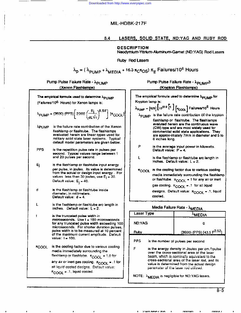
I
* ,..
MIL-HDBK-217F
8.4 LASERS, SOLID STATE, ND:YAG AND RUBY ROD
DESCRIPTIONNeocfymium-Ytt~m-AbminurnGamet (ND:YAG) Rod Lasers
Ruby Rod Lasers
+)= ( ‘p”~~ +‘MEDIA + 16.3 xc~s) ~E Failures/l 06 Hours
Pump Pulse Failure Rate - kpuMpfXannn Fla=hlarrmm\1 -------- . --- . . . . .-,
The empiricalfmula used to determine~UMp(Failures/1@ Hours) for Xenon lamps is:
[ (d,k) ] ~nm,+WMP = @~) (PPS) 2000 k 8058
@lJfvIp k the failure rate contribution of the xenonflashlamp or flashtube. The flashlampsevaluated herein are linear types used formilitarysolid state laser systems. Typicaldefautt model parameters are given below.
PPS is the repetition pulse rate in pulses persecond. Typbal values range between 1and 20 pulses per second.
Ej is the fkwhlamp or flashtube input energyper pulse, in joules. Its value is determinedfrom the actual or desgn inputenergy . Forvalues less than 30 @Jes, use Ej = 30.Default value: E = 40.j
d is the flashlamp or flashtube insidediameter, in millimeters.Default value: d = 4.
L is the flashlamp or flashtube arc length ininches. Default value: L = 2.
t is the truncated pulse width inmicroseconds. Use t -100 microsecondsfor any truncatd pulse width exceeding 100microseconds. For shotier duration pulses,pulse width is to be measured at 10 percentof the maximum current amplitude. Defauttvalue: t = 100.
xc~L is the cooling factor due to various coolingmedia immediately surrounding theflashlamp or flashtube, ~~~L = 1.0 for
any air or inefl gas cooling, ~C@L = .1 forail liquid cooled designs. Default value:
‘COOL = .1, Iquid cooled.
Pump Pulse Failure Rate - kpUM@IKnmtnn Ftaehla~},. ... ~.-.. . .-w. ..-. .~v,
The empirical formula used to determine *MP forKtypton lamp is:
~p - [625][,0(”$’9 1[ ]km Failures/l 06 Hours
kpUMp is the failure me contributionOf the kryptonflashlamp or flashtube. me flashlampsevalutad herein are the continuouswave(CW) type and are mostwidelyused forcommercial solid state applkations. Theyare approx-imatety7mm indiameter and 5 to6 inches brig.
P is the average inputpower in Idbwatts.Default value: P =4.
L is the flashlamp or flashtube arc length ininches. Defautt value: L -2.
Zca is the woling factor due to various cooling
media immediately surrounding the flashlampor fkht~. ~~L = 1 for a~ air or inert
gas cooling. n- -.1 for all liquiddesigns. Defautt va!ue: ~c~L = .1, liquidcooled.
Meda Failure Rate - ~EDiA
Laser Type ‘MEDIA
ND:YAG o
R~ _ (3600) (PPS) [43.5 F2052~)
PPS is the number of pulses per second
F is the energy density in Joules per cm. z/pulseover the cross-sectional area of the laserbeam, which is nominalty equivalent to thecross-sectional area of the laser rod, and itsvalue is determined from the actual designparameter of the laser rod utilized.
NOTE: ~MEDIA is negligible for ND:YAG lasers.
8-5
Downloaded from http://www.everyspec.com
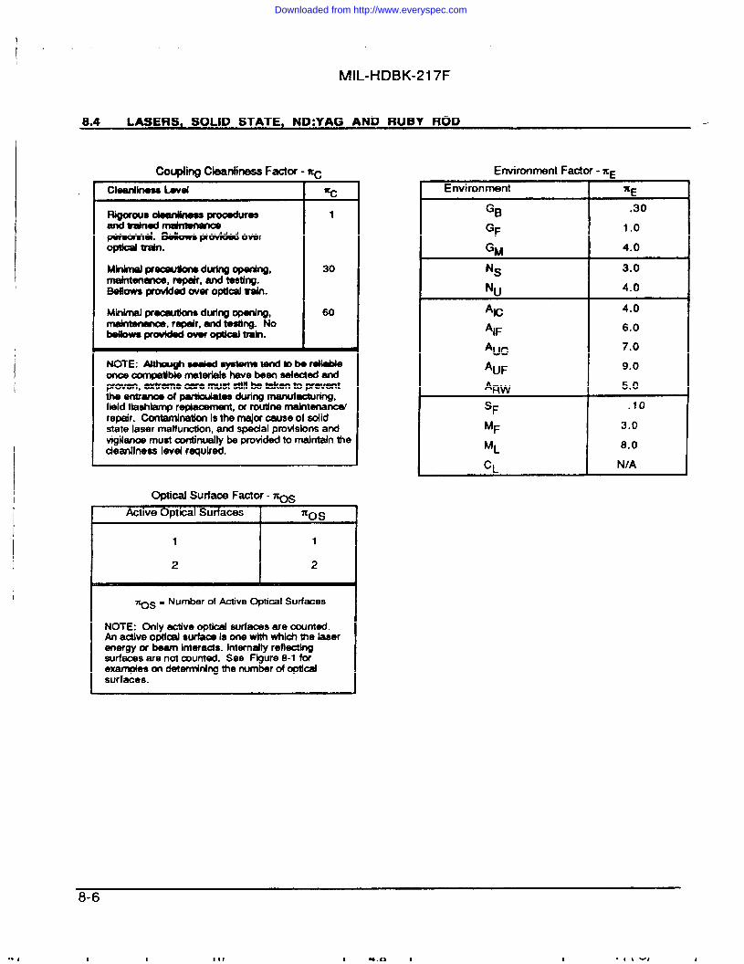
I
MIL-HDBK-217F
8.4 LASERS, SOLID STATE, ND:YAG AND RUBY ROD —
CouplingCleadinassFactor - -z Environment Factor “~E
CleardinessLovd %
Rk3#ltml#c&&s ~-r- 1
~d. BOUOWBprovidedover~ tin.
Mln&nalprmXw$Orwdwing opaning, 30makltananoe, mpdr, and testing.Bellows prddad Ovw Optkat train.
Minimal pr~ons duringopening, 60mdntorumca, repair,and ta8drg. Notx?lbw,prOvWxfOvu ~ train.
NOTE: Mhoughsodod qsternstendmberelMleOnoeCompatiblematerialshavebeenSeh30tedandproven,extremecaremuststtltbe takento prevsntthe entranoeof partkdatesduringmanufacturing,field ftashlamp repkemmt, or routinemaintenancerepair. Contamhatkm is the major cause of solidstate lasermatfurx3ion, and spedal provlsbns andvigilanoemust oontirwaltybe provided to maintain thedeanllness level required.
Optioal Surfaoe Factor - ~SActive Optical Surfaces ‘0s
1 1
2 2
~s = Numbr ofActiveOptical Surfaces
NOTE: Onlyactiveoptioalsurfmmsare munted.Anactiveopticalsurfaceis onewithwhid the iaserenergyor beam interacts.Internallyreflectingsurfacesare notcxxmted.See Figure8-1 forexamphw on dettinlng the number of OPUcatsurfaces.
—Environment %E
GB .30
GF 1.0
GM 4.0
Ns 3.0
Nu 4.0
Ac 4.0
AF 6.0
%c 7.0
‘UF 9.0
‘RW 5.0
SF .10
MF 3.0
ML 8.0
CL N/A
8-6
Downloaded from http://www.everyspec.com
9 . ,,, . .
MIL-HDBK-217F
9.0 RESISTORS, INTRODUCTION
This section includes the active resistor specificationsand, in addition, some eider/inactive specificationsare included because of the large number of equipments stilt in field use which oontain these parts.
The Established Reliability (ER) resktor family generaity has four qualification failure rate levels whentested per the requirements of the appikabie specification. These quaiiitbn failure rate levels difier bya factor of ten (from one level to the next). However, field data has shown that these failure rate levelsdiffer by a factor of about only three, hence the ~ values have been set accordingly.
The use of the resistor modek requires the calculation of the electrfcat power stress ratio, Stress =-~ Pow@r/~t~~er,orPr~9.16 for variable msktors. The models have been structuredsuch that derating curves do not have to be used to find the base failure rate. The rated IXWer for thestress ratb is ~al to the full nominal rated power of the resistor. For example, a MlL-R_ resistor hasthe foiiowing derating cume:
100
80
60
40
20
00 40 80 120
AMBlENT TEMPERATURE INDEGREES CELSIUS
Figure 9-1: MIL-Ft-39006 Deratlng Curve
This particular resistor has a rating of 1 watt at 70”C arrtknt, or below. If Itwere behg used in an an’k#enttemperature of 10O°C, the rated power for the stress calculation would still be 1 watt, ~ 45% of 1 watt (asread off the curve for 100*C). Of course, while the deratlng cuwe k not needed to determine the basefailure rate, it nmst still be observed as the maxinum operating condtbn. To aid in detenMing if a resistoris being used within rated conditions, the base failure rate tables show entries up to certain combinationsof stress and temperature. If a given operating stress and temperature point faits in the blank portion ofthe base failure rate table, the resistor is ovemtmssed. Such wisappfbatbn wouid require an anatysis ofthe circuit and operating conditions to bring the resistor within rated conditions.
9-1
Downloaded from http://www.everyspec.com
I
MIL-I+DBK-217F
9.1 RESISTORS, FIXED, COMPOSITION
SPECIFICATION STYLE DESCRIPTIONMIL-R-39008 RCR Resistors, Fixed, Composition (Insulated), Established ReliabilityMIL-R-11 RC Resistors, Fixed, Composition (Insulated)
Base Failure Rate - ~
Xp s kbXRXQnE Failures/l OGHours
Quality Factor - ~stress-TA (%) .1 .3 .5 .7 .9
0 .00007 .00010 .00015 .00020 .0002810 .00011 .00015 .00021 .00030 ,0004320 .00015 .00022 .00031 .00045 .0006430 .00022 .00031 .00046 .00066 .0009640 .00031 .00045 .00067 .00098 .001450 .00044 .00066 .00098 .0014 .002160 .00063 .00095 .0014 .0021 .0032
.00090 .0014 .0021 .0032 ,0048;: .0013 .0020 .0031 .004790 .0018 .0029 .0045100 .0026 .0041 .0065110 .0038 .0060120 .0054
( (W))exff?(-))%=4.5x 10-gexp 12
T= Ambient Temperature (“C)
s= Ratio of Operating Power to Rated Power
Resistance Factor - ~RResistance Range (ohms) ~R
<.l M 1.0
>.l Mtol M 1.1
>l.OMtol OM 1.6
>1OM 2.5
Quality
s
R
P
M
MlL-R-l 1
Lower
7CQ
.03
0.1
0.3
1.0
5.0
15
Environment Factor - ~EEnvironment
GB
GF
GM
Ns
Nu
‘Ic
‘IF
%c
*UF
‘RMISF
MF
ML
CLb
—~E
1,03.0
8.0
5.0
13
4.0
5.0
7.0
11
19
.50
11
27
490
9-2
----- ——-- -—1- r.llauLe Lila L aullclllu LAG u&uw*, .y” *u b..*-- ~-----
Downloaded from http://www.everyspec.com
MIL-HDBK-217F
9.2 RESISTORS, FIXED, FILM
SPECIFICATION STYLEMIL-R-39017 RLRMIL-R-22684 RLMIL-R-55182 RN (R, C, or N)MIL-R-105O9 RN
Base Failure Rate - ~IMIL-R-22684 and MIL-R-990171....—.- ——-- ----- ...._ .._ --- . I
TA (%) .1 .3 .5 .7 .9
0 .00059 .00073 .00089 .0011 .0013
10 .00063 .00078 .00096 .0012 .0014
20 .00067 .00084 .0010 .0013 .0016
30 .00072 .00090 .0011 .0014 .0018
40 .00078 .00098 .0012 .0016 .0019
50 .00084 .0011 .0014 .0017 .0022
60 .00092 .0012 .0015 .0019 .0024
70 .0010 .0013 .0017 .0021 .0027
80 .0011 .0014 .0018 .0024
90 .0012 .0016 .0021 .0027
100 .0013 .0018 .0023
110 .0015 .0020 .0026
120 .0017 .0023
130 .0019
140 .0022
-
~=3.25x 10⁴ .xp(*)’exf(=))
T = Ambient Temperature (oC)
S = Ratio of Operating Power to Rated Power
DESCRIPTIONFixed, Film, Insulated, Established ReliabilityFued, Film, InsulatedFixed, Film, Established ReliabilityFixed, Film, High Stability
Failures/l OGHours
TA (Z:
o10203040
5060708090100110120
130140150160170
Base Failure Rate - ~[MIL-R-10509 and MIL-R-551 82)
.1 .3 .5 .7 .9
.00061 .00074 .00091 .0011 .0014
.00067 .00082 .0010 .0012 .0015
.00073 .00091 .0011 .0014 .0017
.00080 .0010 .0013 .0016 .0019
.00088 .0011 .0014 .0017 .0022
.00096 .0012 .0015 .0020 .0025
.0011 .0013 .0017 .0022 .0028
.0012 .0015 .0019 .0025 .0032
.0013 .0016 .0021 .0028F
.0014 .0018
F
.0024 .0031 .0040.0015 .0020 .0026 .0035 .0045.0017 .0022 .0029 .0039 .0051.0018 .0024 .0033 .0043 .0058
z~~ =; 0065.0024 .0033 .0045.0026 .0036.0029
(“(=Y”XPP(-))~= 5x10⁻⁵exp 35
T. AmbientTemperature (°C)
s. Ratio of Operating Power to Rated Power
NOTE: Do not use MlL-R-l 0509 (Characteristic B)below the line. Points below are overstressed.
9-3
Downloaded from http://www.everyspec.com
I
I
MIL-HDBK-217F
9.2 RESISTORS, FIXED, FILM
Resistance Factor - ~n,,Resistance Range (ohms) lc~
<.l M 1.0
>().lMtOIM 1.1
>l.OMtol OM 1.6
>IOM 2.5
QuaJ-~ Factor - ~Quality lt~
s .03
R 0.1
P 0.3
M 1.0
MlL-R-l 0509 5.0
MIL-R-22684 5.0
Lower 15
Environment Factor - ~Environment
GBGF
NsNu
*IC‘IF
*UC
*UF
%+/vSF
MF
ML
c,
b
~E
1.02.0
8.0
4.0
14
4.0
8.0
10
18
19
.20
10
28
510 I
9-4
Downloaded from http://www.everyspec.com
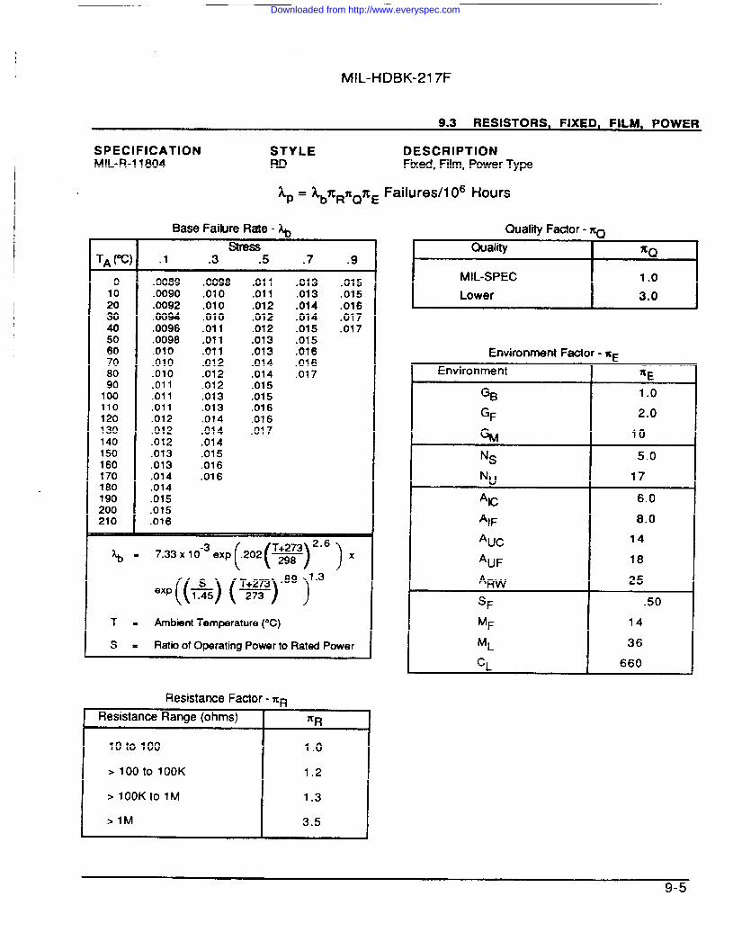
MIL-HDE3K-217F
9.3 RESISTORS, FIXED, FILM, POWER
SPECIFICATION STYLEMIL-R-11804 RD
Ap = kb7cRz*7cE
Base Failure Rate - ~stress -
TA (%) .1 .3 .5 .7 .9
0 .0089 .0098 .011 .013 .01510 .0090 .010 .011 .013 .01520 .0092 .010 .012 .014 .01630 .0094 .010 ,012 .014 .01740 .0096 .011 .012 .015 .01750 .0098 .011 .013 .01560 .010 .011 .013 .01670 .010 .012 .014 .01680 .010 .012 .014 .01790 .011 .012 .015100 .011 .013 .015110 .011 .013 .016120 .012 .014 .016130 .012 .014 .017140 .012 .014150 .013 .015160 .013 .016170 .014 .016180 .014190 .015200 .015210 .016&
%=(- (*)2’) x
7.33 x 10⁻³ exp 202
‘xp((~) (=)”8’)’3
T= Ambient Temperature (“C)
s= Ratio of Operating Power to Rated Power
Resistance Factor - ZRResistance Range (ohms) x~
lo to 100I
1.0
> 100to 100K I 1.2
>lOOKtol M I 1,3
>lM I 3.5
DESCRIPTIONFued, Film, Power Type
Failures/l OGHours
QuaIii Factor - ~Quality %Q
!
II
MIL-SPECLower
II
1.0
3.0II
Environment Factor - x=\
Environment
GB
GF
GM
Ns
NU
*IC
‘IF
*UC
*UF
‘RW,SF
MF
ML
C’
2.0
10
5.017
6.08.014
18
25
.5014
36
660
9-5
---
Downloaded from http://www.everyspec.com
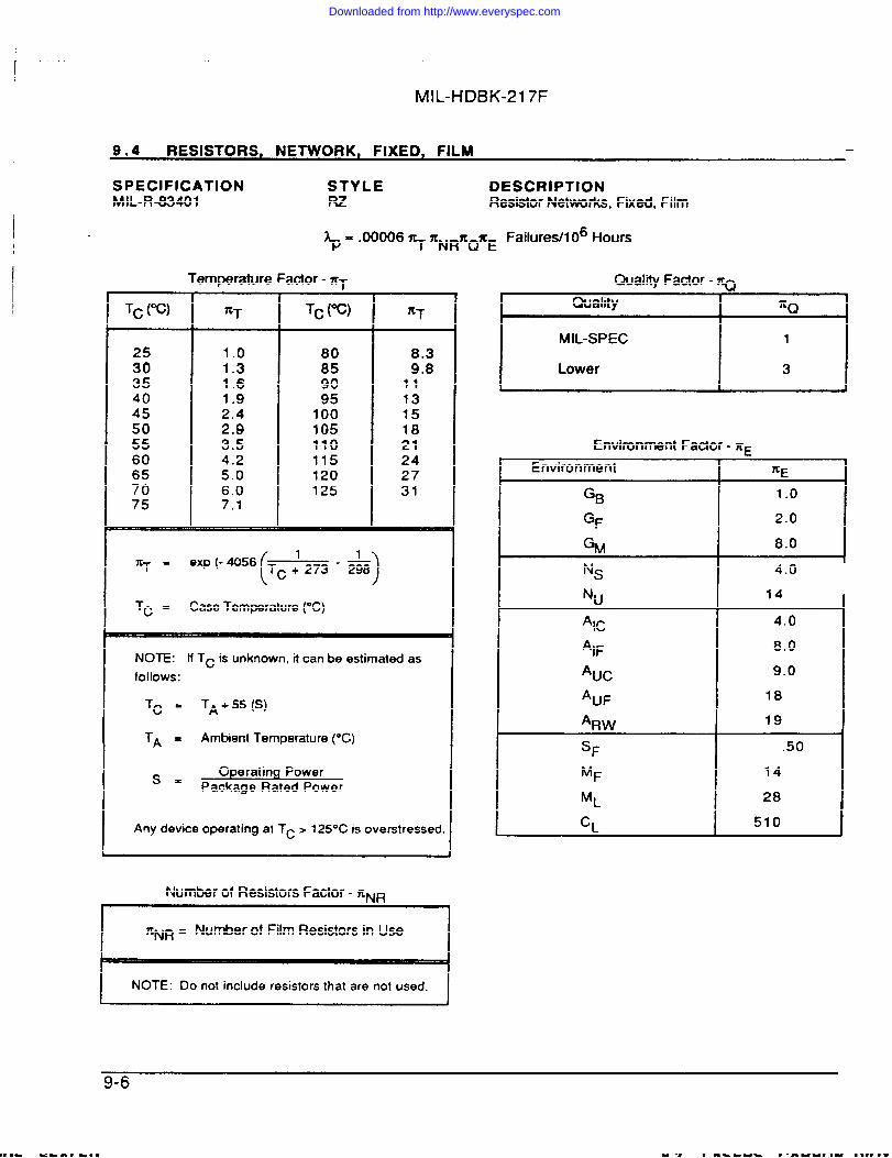
i’”’ . .
MIL-HDBK-217F
9.4 RESISTORS, NETWORK, FIXED, FILM
SPECIFICATION STYLE DESCRIPTIONMIL-R-83401 Rz Resistor Networks, Fixed, Film
~= .00006 ~ ZNRZQXE Failures/106 Hours
2530354045505560
%75
Temperature Factor - XT.
1.01.31.61.92.42.93.54.25.06.07,1
TC (Z)
80859095100105110115120125
\“ )
Tc = Case Temperature (“C)
8.39.81113151821242731
NOTE: If Tc is unknown, it can be estimated asfollows:
TC = TA + 55 (S)
TA = Ambient Temperature (°C)
s= Operating PowerPackage Rated Power
Any device operating at TC > 125°C is overstressed.
Number of Resistors Factor - ~NR
I ‘NR = Number of FilmResistorsin UseI
I NOTE: Do not include resistors that are not used. I
Quality Factor - ~Quality ! 7CQ
I MIL-SPEC I “ 1I Lower
I3
Envirmment Factor - n=Environment
GBGFGMN~
Nu
‘Ic
‘IF
‘Uc
‘UF
‘RWSF
MF
ML
c,
~E
1.0
2.0
8.01
4.0
14
4.0
8.0
9.0
18
19
.50
14
28
510
9-6
Downloaded from http://www.everyspec.com
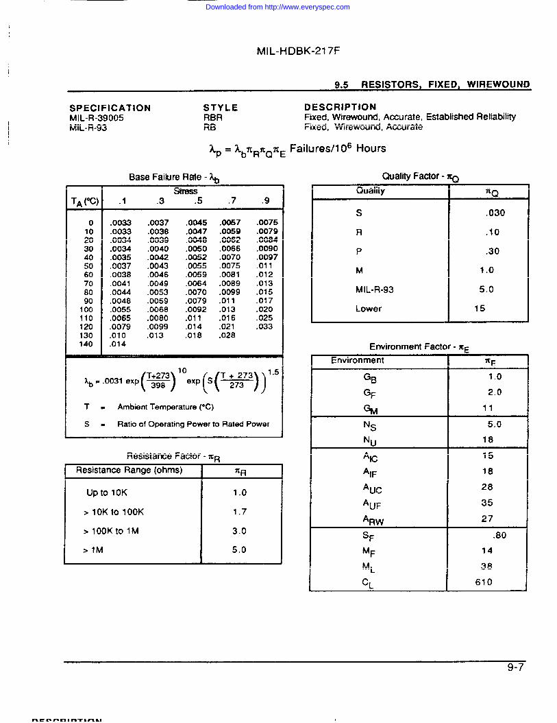
MIL-HDBK-217F
9.5 RESISTORS, FIXED, WIREWOUND
SPECIFICATION STYLE DESCRIPTIONMIL-R-39005 RBR Fixed, Wlrewound, Accurate, Established ReliabilityMIL-R-93 RB Fixed, Wirewound, Accurate
Xp = lbnRZQnE Failures/l OGHours
Quality Factor - ~Base Failure Rate - ~str13s -
TA (W) .1 .3 .5 .7 .9
0 .0033 .0037 .0CM5 .0s7 .0075.0033 .0038 .0047 .0059 .0079
% .0034 .0039 .0048 .0062 .008430 .0034 .0040 .0050 .0066 .009040 .0035 .0042 .0052 .0070 .009750 .0037 .0043 .0055 .0075 .01160 .0038 .0046 .0059 .0081 .01270 .0041 .0049 .0064 .0089 .01380 .0044 .0053 .0070 ,0099 .01590 .0048 .0059 .0079 .011 .017100 .0055 .0068 .0092 .013 .020110 .0065 .0080 .011 .016 .025120 .0079 .0099 .014 .021 .033130 .010 .013 .018 .028140 .014
m
(T+273)loexpp(T;g3) )15~. .0031 exp 398
T- Ambient Temperature (oC)
s= Ratio of Operating Power to Rated Power
Resistance Factor - ~R
Resistance Range (ohms) ~R
Up to 10K 1.0
> 10Kto 100K 1.7
>lOOKtol M 3.0
>IM 5.0
Quality
s
R
P
M
MIL-R-93
Lower
7tQ
.030
.10
.30
1.0
5.0
15
Environment Factor - XEEnvironment
GBGFGMN~
Nu
AC
‘IF
*UC
*UF%w
SF
MF
ML
c,
2.0
11
5.0
18
15
18
28
35
27
.8014
38
610
9-7
Downloaded from http://www.everyspec.com
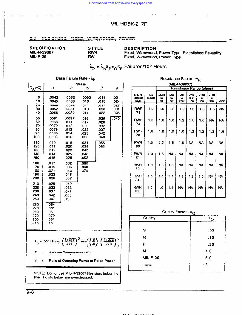
I4 ,, . . . . . ,, .
MIL-HDBK-217F
9.6 RESISTORS, FIXED, WIREWOUND, POWER
SPECIFICATION STYLE DESCRIPTIONMIL-R-39007 Fixed, WireWound, Power Type, EstablishedRelkbNtyMIL-R-26 Fixed, Wirewouruf, Power Type
~ = hb7c#Q7t~ Failures/l OGHours
Base Failure Rate - &.Stress
TA (“C) .1 .3 .5 .7 .9
.0042 .0062 .0093 .014 .0211: .0045 .0068 .010 .016 .02420 .0048 .0074 .011 .017 .02730 .0052 .0081 .013 .020 .03140 .0056 .0089 .014 .022 .03550 .0081 .0097 .016 .025 .ti–60 .0066 .011 .017 .02870 .0072 .012 .020 .03280 .0078 .013 .022 .03790 .0085 .014 .025 .042100 .0093 .016 .028 .048110 .010 .018 ,031 .055120 .011 .020 .036 .063130 .012 .022 .040140 .014 .025 .046150 .015 .028 .052160 .017 .032 .060170 .019 ,036 .068180 .021 .040 .078
.023 .046X% .026 .052210 .029 .059220 .033 .068230 .037 .077240 .042 .088250 .047 ,10260 .054270 .061280 .06290 .079300 .091310 .10
~-M148eXP(~)2ex@) (=))
T= Ambient Temperature (“C)
s= Ratio of Operating Power to Ftatad Power
NOTE: Do not use MlL-R-39oo7 Resistors below theline. Points below are overstressed.
Siyte
71
74
78
80
81
82
84
89
upbsoc
1.0
1.0
1.0
1.0
1.0
1.0
1.0
1.0
Resistance Factor - ZR(MIL-R-39007)Re ) Ra[
●s00
1:
1.0
1.0
1.0
1.2
1.6
1.6
1.0
1.0
>1K
z1.2
1.0
1.0
1.6
NA
1.6
1.1
1.4
istan
s
7!3(
1.2
1.2
1.0
1.6
NA
NA
1.2
NA
*75KkJ1*
1.6
1.6
1.2
NA
NA
NA
1.2
NA
Quality Factor - nQQuality
sR
P
M
MIL-R-26
Lower
w>Iw
I&
1.6
1.6
1.2
NA
NA
NA
1.6
NA
*
>19(
&1.6
NA
1.2
NA
NA
NA
NA
NA
NA
N/l
1.6
NA
NA
NA
NA
MA
KQ
.03
.10
.30
1.0
5.0
15
I
--Y-u
Downloaded from http://www.everyspec.com
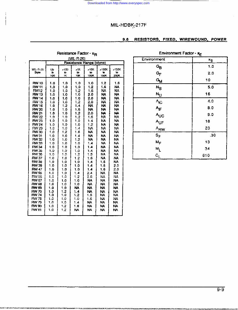
MIL-HDBK:217F
9.6 RESISTORS, FIXED, WIREWOUND, POWER
MIL-R-26
Rw 10RwllRW12Rw 13Rw 14Rw 15RW16RW20Rw 21
KERW 24RW 29RW30Rw 31RW32
ZE
EERw 37
E:Rw 47RW55RW56RW 67
l%:Rw 70Rw 74Fw 70
R:RW 81
Resistanm Factor - XR(MIL-R-2
Resistance
ups100
1.0t .01.01.01.01.01,01.01.01.01.01.01.01.01.01.01.01.01.01.01.01.01.01.01.01.01.01.01.01.01.01.01.01.01.0
>100mIK
1.01.01.01.01.01.01.21.01.01,01.01.01.01.21.01.01.01.01.01.01.01.01.01.01.01.01.01.01.01.21.01.01.01.21.2
>1KtoICM
1.0
1.01.21.01.0
;::1.61.21.21.01.01.41.61.41.21.01.01.01.21.21.01.01.01.41.21.01.0NA1.4
;::1.41.6NA
mge I
>1OKto
100K
1.01.21.62.02.02.0NANA2.01.61.41.2
I&NANA1.41.41.41.51.61.41.41.42.42.6
ENAW1.61.6NANANA
]ms)
*lab
I!iw
1.21.6M
E
ENANANANANA
KNANA
$NANANA1.61.61.6NA
K
ENA
ENA
E
>150K
J%1.6NANA
E
KNAWANANANA
ENANA
ENA
$NA2.02.0NANA
KNANA
K
KNA
Environment Factor - ~Environment ~E
GB 1.0
GF 2.0
% 10
NS 5.0
NU 16
‘Ic 4.0
‘IF 8.0
‘Uc 9.0
*UF 18
‘Rw 23
SF .30MF 13ML 34CL 610
9-9
Downloaded from http://www.everyspec.com
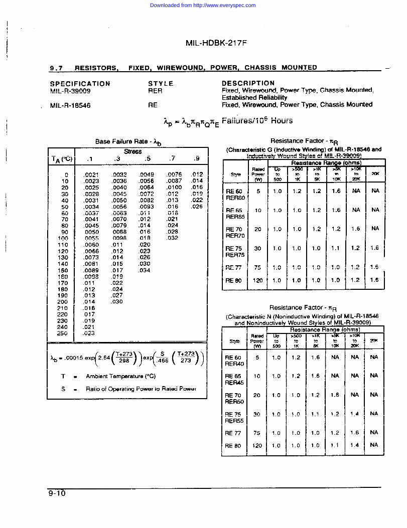
MIL-HDBK-217F
9.7 RESISTORS, FIXED, WIREWOUND, POWER, CHASSIS MOUNTED
SPECIFICATION STYLE DESCRIPTIONMIL-R-39009 RER Fixed, Wirewound, Power Type, Chassis Mounted,
Established Reliability. MIL-R-18546 RE Fixed, Whewound, Power Type, Chassis Mounted
Base Failure Rate - ~ Resistance Factor - ZR
stress -TA (Z) .1 .3 .5 .7 .9
0 .0021 .0032 .0049 .0076 .01210 .0023 .0036 .0056 .0087 .01420 .0025 .0040 .0064 .0100 .01630 .0020 .0045 .0072 .012 .01940 .0031 .0050 .0082 .013 .02250 .0034 .0056 .0093 .016 .02660 .0037 .0063 .011 .01870 .0041 .0070 .012 .02180 .0045 .0079 .014 .02490 .0050 .0088 .016 .028100 .0055 .0098 .018 .032110 .0060 .011 .020120 .0066 .012 .023130 .0073 .014 ,026140 .0081 .015 .030150 .0089 .017 .034160 .0098 .019170 .011 .022180 .012 .024190 .013 .027200 .014 .030210 .016220 .017230 .019240 .021250 .023
4
( (%)ex(a’a)~ = .00015 exp 2.64
T= Ambient Temperature (“C)
s= Ratio of Operating Power to Rated Power
(CharacteristicG (tnductiveWinding ti MlL-R-l 8546 andKmotr
RatedPowar
5
10
20
30
75
120
lL-R-
+10
c)IOK
1.6
1.6
1.2
1.1
1.0
1.0
1009)mosITz
1.2
1.2
1.2
1.0
1.0
1.0
hms+*1
2%
NA
NA
1.6
1.2
1.2
1.2
XIKStyte toIK
1.2
1.0
1,0
1.0
1.0
1.0
NA
NA
NA
1.6
1.6
RE 60RER60
RE 65RER65
RE 70RER70
RE 75RER75
RE 77
RE 80
1.0
1.0
1.0
1.0
1.0
1.0 1.6I
Resistance Factor - XR(Charaderistic N (NoninductiveWinding)of MIL-R-18546
and Noninc ctively Woun Styles of MILResi: mce Ran e
4Styb
3-39009)
-qr52)1.0
1.0
1.0
1.0
1.0
1,0
T!mitolK
1.2
1.2
1.0
1.0
1.0
1.0
RaledPtxer
5
10
20
30
75
120
E 1;
1.6 NA
1.6 NA
1.2 1.6
1.1 1.2
1.0 1.2
1,0 1.1
20K
NA
M
NA
NA
NA
NA
RE 60RER40
NA
M
NA
1.4
1.6
1.4
RE 65RER45
RE 70RER50
RE 75RER55
RE 80
Downloaded from http://www.everyspec.com
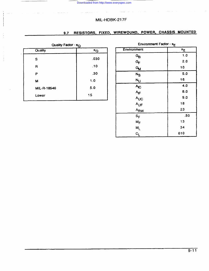
,,. .!.
MIL-HDBK-217F
9.7 RESISTORS, FIXED, WIREWOUND, POWER, CHASSIS MOUNTED
QualityQuality Faotor - ~
s
R
P
M
MIL-R-18546
Lower
.030
.10
.30
1.0
5.0
15
Environment Factor - ~
Environment ~E
GB 1,0
GF 2.0
GM 10
Ns 5.0
Nu 16
AIc 4.0
‘IF 8.0
‘Uc 9.0
*UF 18
‘RW 23
SF .50
MF 13
ML 34
c~ 610
9-11
Downloaded from http://www.everyspec.com
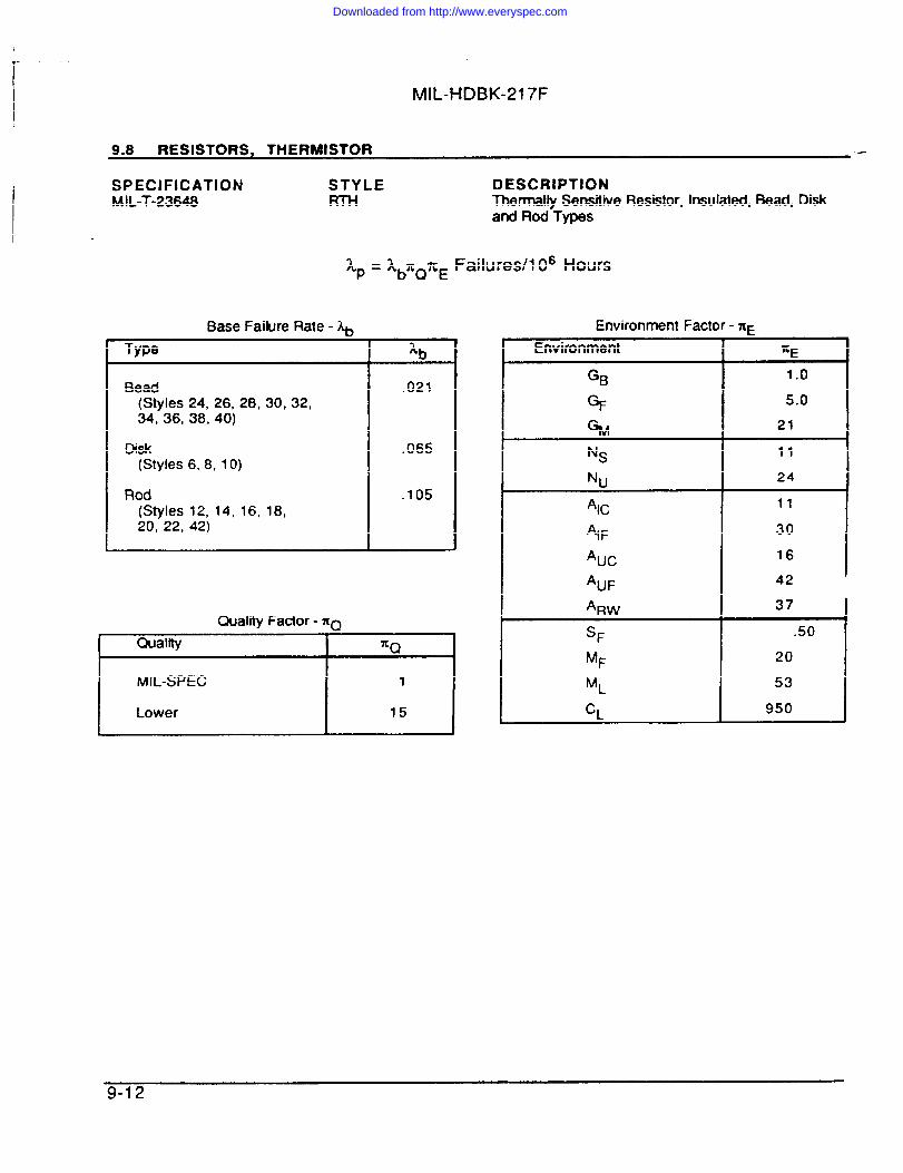
MIL-FIDBK-217F
SPECIFICATION STYLE DESCRIPTIONM IL-T-23648 RTH Thermally Sensitive Resistor, Insulated, Bead, Disk
and Rod-Types
Xp = &QzE Failures/l OGHours
Base Failure Rate - ~—Type A~
Bead .021(Styles 24, 26,28,30,32,34, 36, 38, 40)
Disk .065(Styles 6,8, 10)
Rod .105(Styles 12, 14, 16, 18,20, 22, 42)
Quality Factor - fl~Quality ~Q
MIL-SPEC 1
Lower 15
Environment Factor - xzEnvironment
GBGF
%Ns
Nu
‘Ic
‘IF
‘Uc
‘UF
‘RWSF
MF
ML
c,
L
~E
1.0
5.0
21
11
24
11
30
16
42
37
.50
20
53
950
9-12
Downloaded from http://www.everyspec.com
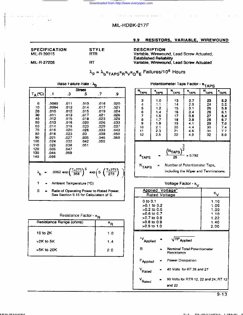
i
....,. . . . . .. . . . . .,. . . . . .. . .,, ..*.
1MIL-tiDBK-217F
9.9 RESISTORS, VARIABLE, W! REWOUND
SPECIFICATION STYLE DESCRIPTIONI MIL-R-39015 Iv-R Variable, Wtrewound, Lead Screw Actuated,
Established ReliabilityMIL-R-27208 RT Variable, Wkewound, Lead Screw Actuated
I o
;30405060708090100110120130140
l--.
Xp = kbfiTAp~XRZvXQzE Failures/l OGHours
Base Failure Rate - ~stress
.1 .3 .5 .7 .9
.0089 .011
.0094 .012
.010 .012
.011 ,013
.012 .015
.013 .016,014 .018.016 .020.018 .023.021 .027.024 .032.029 .038.035 .047.044 .059.056
.013 .016 .020
.014 .017 .021
.015 .019 .024
.017 .021 .026
.018 .023 .029
.020 .026 .033
.023 .029 .037
.026 .033 .043
.03 .039 .050
.035 .046 .060
.042 .055
.051
%- 0062”’’(=?’‘X’(S(T=);
T - Ambient Temperature (“C)
s = Ratio of Operating Power to Rated Power.See Section 9.16 for Calculation of S.
Resistance Factor - XR
I Resistance Range (ohms) I %10t02K 1.0
>2K to 5K 1.4
>5K to 20K 2.0
Potentiometer Taps Factor - q~o=snr g
NTAPS
N‘TAPS TAPS ‘TAPS
NTAPS ‘TAPS
3 1.0 13 2.7 23 5.24 1.1 14 2.9 5.55 1.2 15 3.1 z 5.86 1.4 16 3,4 6.17 1.5 17 3.6 E 6.4a 1.7 18 3.8 6.79 1.9 19 4.1 :: 7.010 2.1 20 4.4 30 7.411 2.3 21 4.6 31 7.712 2.5 22 4.9 32 8.0
=’2
%APS = 2S + 0.792
‘TAPS = Number of PotentiometerTaps,includingthe Wiper and Terminations. ~
I
Voltage Factor - xv
Applied Voltage*Rated Voltage ‘%
Otoo.1>0.1 to 0.2>0.2 to 0.6>0.6 to 0.7>0.7 to 0.8>0.8 to 0.9>0.9 to 1.0
1.101.051.001.101.221.402.00
w Applied = ~RpApplied
R = Nominal Total PotentiometerResistance
‘Applied = Power Dissipation
‘Rated -40 Volts for RT 26 and 27
vRated = 90 Votts for RTR 12, 22 and 24; RT 12
and 22
Downloaded from http://www.everyspec.com
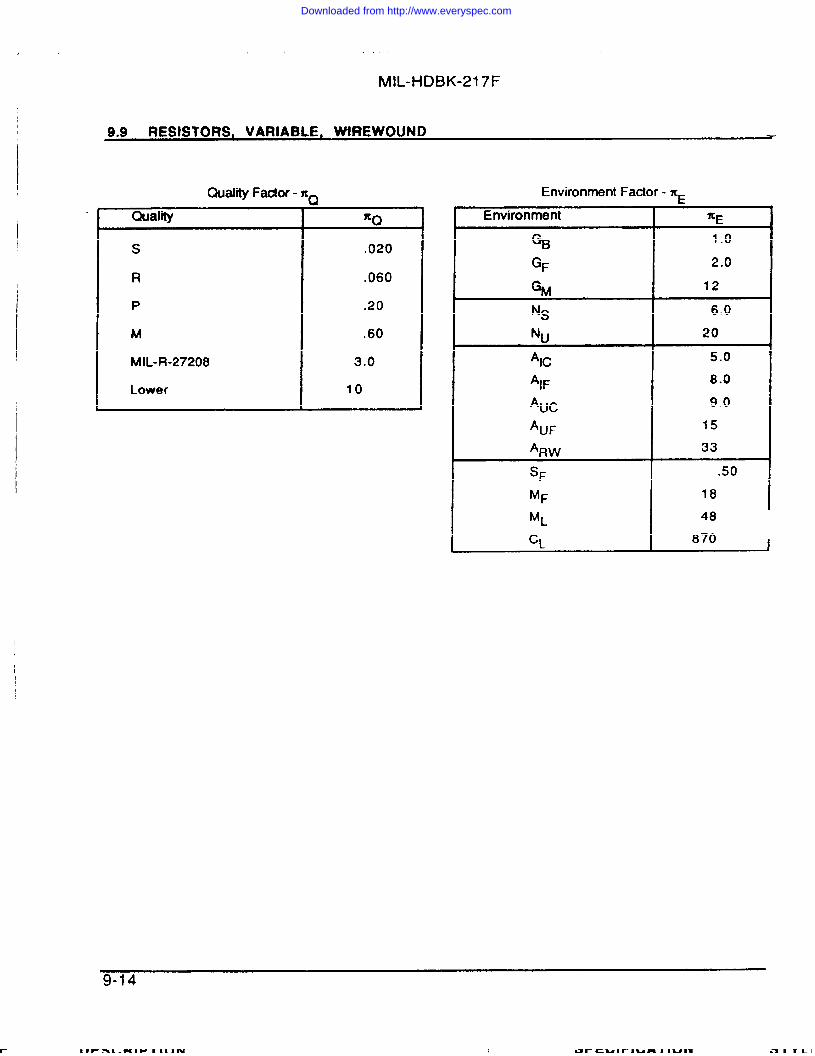
MIL-HDBK-217F
I
9.9 RESISTORS, VARIABLE, WIREWOUND 7
QualityFactor - nfiu
Quality I %Q
sR
P
M
MIL-R-27208
Lower
.020
.060
.20
.60
3.0
10
Environment Factor - KG
Environment
%GF
%...Ns
Nu
‘Ic‘IF
‘Uc
‘UF
‘RW
SF
MF
ML
cl
L
~E
1.0
2.0
12
6.0
20
5.0
8.0
9.0
15
33
.50
18
48
870
9-14
Downloaded from http://www.everyspec.com
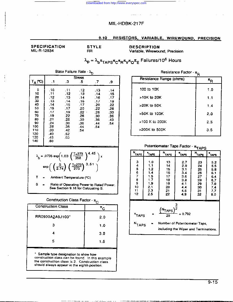
I
/
.! .,,
1 MIL-HDBK-217F
9.10 RESISTORS, VARIABLE, WIREWOUND, PRECISION
SPECIFICATION STYLE DESCRIPTIONMIL-R-12934 RR Variable, WIrewound, Precision
o
E30405060708090100110120130140
Base Failure Rate - ~stress
.1 .3 .5 .7 .9
.10
.11
.12
.13
.14
.15
.17
.19
.21
.24
.28
.33
.40
.49
.60
.11 .12 .13 .14
.12 .13 .14 .15
.13 .14 .16 .17
.14 .16 .17 .19
.15 .J7 .20 .22
.17 .20 .22 .26
.19 .22 ‘ .26 ,30
.22 .26 .30 .36
.25 .30 .36 .43
.30 .36 .44 .54
.35 .44 .54
.42 .54
.52
.65
\ ( (~ )4.45)X-.0735 exp 1.03
exp((z%) (*)351)
T= Ambient Temperature ~C)
s. Ratio of Operating Power to Rated Power.See Section 9.16 for Calculating S.
ConstructionClass Factor - z=b
f ConstructionClass I 7K*
RR0900AZA9J1 03” 2.0
3 1.0
4 3.0
5 1.5
“ Sample type designation to show howconstruction class can be found, In this examplethe construction cJass is 2. Construction classshould always appear in the eighth position.
Resistance Factor -ResistanceRange (ohms)
100 to IOK
>?OKto 20K
>20K to 50K
>50K to 10OK
>100 K to 200K
>200K to 500K
R
‘R
1.0
1.1
1.4
2.0
2.5
3.5
Potentbrneter Taps Factor - ?AP:‘TAPS
1.01.11.21.41.5
;::2.1
:::
NTAPS
1314151617181920
:;
3
‘TAPS
$:;
:::3.63.84.14.4
:::
‘TAPS
5.25.55.86.16.46.77.07.4
;;:
M5 .(-),,,
‘%APS = 25 .
‘TAPS - Number of Potentiometer Taps,
including the W@er and Terminations.
Downloaded from http://www.everyspec.com
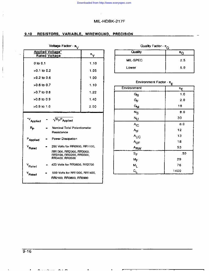
MIL-HDBK-217F
9.10 RESISTORS, VARIABLE, WIREWOUND, PRECISION —
Vottage Factor - ~Applied Voltage’Rated voltage ‘%
o to 0.1 1.10
>0.1 to 0.2 1.05
>0.2 to 0.6 1.00
>0.6 to 0.7 1.10
>0.7 to 0.8 1.22
>0.8 to 0.9 1.40
>0.9 to 1.0 2.00
“vApplied ==
RP - Nominal Total PotentiometerResistance
‘Applied 9 Power Dissipation
v Rated = 250 Votts for RR0900, RRI 100,
RR1300, RR2000, RR3000,RR31OO, RR3200, RR3300,RR3400, RR3500
v Rated . 423 Volts for RR3600, RR3700
‘Rated - 500 Votts for RR1 000, RR1 400,
RR21 00, RR3600, RR3900
Quality Factor- XQQuality *UQ
MIL-SPEC 2,5
Lower 5.0
EnvironmentFactor - n=Environment
GB
GF
GM
Ns
Nu
*IC
‘IF
*UC
*UF
*RWSF
MF
ML
CL
L
1.0
2.0
18
8.0
30
8.0
12
13
18
53
.50
29
76
1400
9-16
Downloaded from http://www.everyspec.com
— ————
MIL-HDBK-21 ;F
I
II
9.11 RESISTORS, VARIABLE, WIREWOUND, SEMIPRECISION
SPECIFICATION STYLE DESCRIPTIONMIL-R-19 RA Variable, Wirewound, Semiprecision (Low Operating
Temperature)MIL-R-39002 RK Variable, WWnvound, Semiprecision
kp = +)~A#R’f/nQnE Failures/l 06 Hours
Base Failure Rate - ~stn?ss “
‘A(~) .1 .3 .5 .7 .9
0 .055 .063 .072 .083 .095
10 .058 .069 .081 .095 .1120 .063 .076 .092 .11 .13
30 .069 .086 .11 .13 ,1740 .076 .098 .13 .16 .21
50 .085 .11 .15 .20 .276070
80:6,1=
90 .16 .26 .42 .69 1.1100 .19 .34 .59 1.0110 .24 .45 .85120 .31130 .42)
\ (- (%)5””).= .0398 exp 514
e+% (*)446 )
T= Ambient Temperature (“C)
s- Ratio of Operating Power to Rated Power,See Section 9.16 for S Calculation.
NOTE: Do not use MlL-R-l 9 below the line. Pointsbelow are overstressed.
Resistance Factor - ZRResistance Range (ohms) I % 110t02K 1.0
>2K to 5K 1.4
>5K to 10K 2.0
Potentiometer Taps Factor - ~APq. . ..-N N‘TAPS NTAPS TAPS ‘TAPS TAPS ‘TAPS
3 1.0 13 2.7 23 5.2
4 1.1 14 2.9 24 5.5
5 1.2 15 3,1 25 5.8
6 1.4 16 3.4 26 6.1
7 1.5 17 3.6 27 6.4
8 1.7 18 3.8 28 6.7
9 1.9 19 4.1 29 7.0
10 2.1 20 4.4 30 7.4
11 2.3 21 4.6 31 7.7
12 2.5 22 4.9 32 8.0
MS2
?APS “ 25 + 0.792
‘TAPS = Number of Potentiometer Taps,
including the Wiper and Terminations.
9-17
Downloaded from http://www.everyspec.com
MIL-HDE3K-217F
9.11 RESISTORS, VARIABLE, WIREWOUND, SEMIPRECISION —
Vottage Factor - ~Applied Voltage*Rated Voltage
Otoo.1
>0.1 to 0.2
>0.2 to 0.6
>0.6 to 0.7
>0.7 to 0.8
>0.8 to 0.9
>0.9 to 1.0
%
1.10
1.05
1.00
1.10
1.22
1.40
2.00
●VApplied =
Rp
‘Applied -
v Rated
-
Nominal Total PotentiometerResistance
Power D~ssipation
50 Votts for RA1o
75 Volts for RA20X-XC, F
130 Volts for RA30X-XC, F
175 Volts for RA20X-XA
275 Volts for RK09
320 Volts for RA30X-XA
Quality Factor - n=
I Quality
MIL-SPEC
Lower
2.0
4.0
Environment Factor - z=
Environment
GBGF
GMN~
Nu
Alc
‘IF
%c
‘UF
‘RWSF
MF
ML
CL
L
1.0
2.0
16
7.0
28
8.0
12
N/A
N/A
38
.50
N{A
N/A
NIA
9-18
I I I I I I I I I I #u 1 . UU I E . U l z . UEU
Downloaded from http://www.everyspec.com
MIL-HDBK-217F
9.12 RESISTORS, VARIABLE, WIREWOUND, POWER
SPECIFICATION STYLE DESCRIPTIONMIL-R-22 RP Variable, Whwound, Power Type
%= &~Ap#R~ZcZ&EFailures/IO’ H..,.
Base Failure Rate - ~Sm?ss “
TA (%) .1 .3 .5 .7 .9
0 .064 .074 .084 .097 .11
10 .067 .078 .091 .11 .12
20 .071 .084 .099 .12 .14
30 .076 .091 .11 .13 .16
40 .081 .099 .12 .15
50 .087 .11 .14 .17
60 .095 .12 .15
70 .10 .14 .18
80 .12 .15
90 .13 .18
100 .15
110 .17
120 .20~
\ ( (T:%)4’6)X= .0481 exp 334
exp(+ (TJ~~)2083)
T. Ambient Temperature (“C)
s= Ratio of Operating Power to Rated Power.See Section 9.16 for S Calculation.
Resistance Factor - nR
I Resistance Range (ohms) I ‘R
1 to 2K 1.0>2K tO 5K 1.4>5K to 10K 2.0
Potentiometer Taps Factor - ~APS., .,-NTAPS N‘TAPS TAPS N‘TAPS TAPS ‘TAPS
3 1.0 13 2.7 23 5.2
4 1.1 14 2.9 24 5.5
5 1.2 15 3.1 25 5.8
6 1.4 16 3.4 26 6.1
7 1.5 17 3.6 27 6.4
8 1.7 18 3.8 28 6.7
9 1.9 19 4.1 29 7.0
10 2.1 20 4.4 30 7.4
11 2.3 21 4.6 31 7.7
12 2.5 22 4.9 32 8.0
us2
%APS = 25 + 0.792
‘TAPS = Number of Potentiometer Taps,
including the W@er and Terminations
9-19
. .-. .A --, I i
Downloaded from http://www.everyspec.com
II MIL-HDBK-217F
9.12 RESISTORS, VARIABLE, WIREWOUND, POWER
Voltage Factor - ~Applied Voltage*Rated Voltage
Otoo.1
>0.1 to 0.2
>0.2 to 0.6
>0.6 to 0.7
>0.7 to 0.8
>0.8 to 0.9
>0.9 to 1.0
‘%
1.10
1.05
1.00
1.10
1.22
1.40
2.00
●v Applied = ~RPpApplied
Rp = Nominal Total PotentiometerResistance
‘Applied = Power Dissipation
‘Rated = 250 Volts for RP06, RP1 O
= 500 Votts for Others
Construction Class Factor - ~
ConstructionClass
Enclosed
Unenclosed
Style - Xc
RP07, RP1l, RP16I 20 I
IIAll Other Styles are 1.0Unenclosed
QualityFactor - XQ
Quality I ~Q
MIL-SPEC I 2.0
LowerI
4.0
Environment Factor - ZE\
Environment I ~EGB 1.0
GF 3.0
GM 16
Ns 7.0
Nu 28
Alc 8.0
‘IF 12
‘Uc N/A
‘UF N/A
*RW 38
I
SF .50
MF N/A
ML WA
cL NIA. b
9-20
Downloaded from http://www.everyspec.com
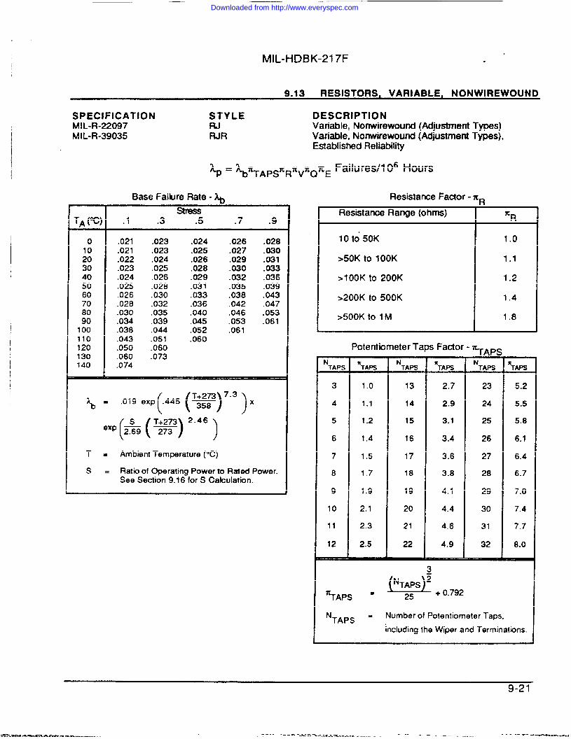
I
II
MIL-HDBK-217F.
.
9.13 RESISTORS, VARIABLE, NONWIREWOUND
SPECIFICATION STYLE DESCRIPTIONMIL-R-22097 RJ Variable, Nonwifewound (Adjustment Types)MIL-R-39035 RJR Variable, Nonwirewound (Adjustment Types),
EstablishedReliability
% = ‘b%APS’R%%’E Failures/l 06 Hours
Base Failure Rate - &smss-
TA (%) .1 .3 .5 .7 .9
0 .021 .023 .024 .026 .028.021 .023 .025 .027 .030
;: .022 .024 .026 .029 .03130 .023 .025 .028 .030 .03340 .024 .026 .029 .032 .03650 .025 .028 .031 .035 .03960 .026 .030 .033 .038 .04370 .028 .032 .036 .042 .047
.030 .035 .040 .046 .053% .034 .039 .045 .053 .061100 .038 .044 .052 ,061110 .043 .051 .060120 .050 .060130 .060 .073140 .074
\= (. (Il&y)x.019 exp 445
.xP(&(T;;r) 246)
T= Ambient Temperature (“C)
s = Ratio of Operating Power to Rated Power.See Section 9.16 for S Calculation.
Resistance Factor - mRResistance Range (ohms) ‘R
10 to 50K 1.0
>50K to 100K 1.1
>IOOK to 200K 1.2
>200K to 500K 1.4
>500K to 1M 1.8
Potentiometer Taps Factor - ‘%APSN NTAPS ‘TAPS TAPS
N‘TAPS TAPS ‘TAPS
3 1.0 13 2.7 23 5.2
4 1.1 14 2.9 24 5.5
5 1.2 15 3.1 25 5.8
6 1.4 16 3.4 26 6.1
7 1.5 17 3.6 27 6.4
8 1.7 18 3.8 28 6.7
9 1.9 19 4.1 29 7.0
10 2.1 20 4.4 30 7.4
11 2.3 21 4.6 31 7.7
12 2.5 22 4.9 32 8.0
MEf2
hAPS = 25 + 0.792
Number of Potentiometer Taps,‘TAPS = ,including the Wiper and Terminations.
9-21
Downloaded from http://www.everyspec.com

I1IMIL-HDBK-217F
9.13 RESISTORS, VARIABLE, NONWIREWOUND —
Voltage Factor - ~Applied Voltage”Rated Voltage *v
Oto 0.8 1.00
>0.8 to 0.9 1.05
>0.9 to 1.0 1.20
“vApplied ==
Rp = Nominal Total PotentiometerResistance
‘Applied = Power Dissipation
vRated = 200 Votts for RJ and RJR26;
RJ and RJR50
= 300 Volts for All Others*
Quality Factor - G
Quality
s .020
R
P
M
MIL-R-22097
Lower
.060
.20
.60
3.0
10
EnvironmentFactor - xcEnvironment
GB
GF
%N~
Nu
Alc
‘IF
AUc
‘UF
‘RWSF
MF
ML
c1
L
~E
1.0
3.0
14
6.0
24
5.0
7.0
12
18
39
.50
22
57
1000
9-22
———__ .— _ _
Downloaded from http://www.everyspec.com
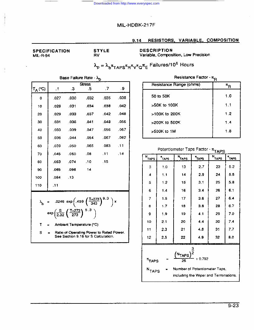
MIL-HDBK-217F
9.14 RESISTORS, VARIABLE, COMPOSITION
SPECIFICATION STYLE DESCRIPTIONMIL-R-94 RV Variable, Composition, Low Precision
I
TA (%)
o
10
20
30
40
50
60
70
80
90
100
110
Lp = ‘#TAp&#f/nQnE Failures/l OG Hours
Base Failure Rate - ~
Stress.1 .3 .5 .7 .9
.027
.028
.029
.031
.033
.036
.039
.045
.053
.065
.084
.11
.030
.031
.033
.036
.039
.044
.050
.060
.074
.096
.13
.032
.034
.037
.041
.047
.054
.065
.08
.10
,14
.035
.038
.042
.048
.056
.067
.083
,11
.15
.038
.042
.048
.056
.067
.082
.11
.14
%= [. (*)9.3-)X.0246 13XP 459
.xp(&(w)” )
T- Ambient Temperature (“C)
s = Ratio of OperW!ng Power to Rated Power,See Section 9.16 for S Calculation.
Resistance Factor - Xn. .Resistance Range (ohms)
50 to 50K
>50K to lOOK
>1OOKto 200K
>200K to 500K
>500K tO 1M
NTAPS
3
4
5
6
7
0
9
10
11
12
1.0
1.1
1.2
1.4
1,8
Potentiometer Taps Factor - ~AP:
7‘TAPS‘TIW
1.0
1.1
1.2
1.4
1.5
1.7
1.9
2.1
2.3
2.5
NTAPS
13
14
15
16
17
18
19
20
21
22
‘TAPS
2.7
2.9
3.1
3.4
3.6
3.8
4.1
4.4
4.6
4.9
NTAPS
23
24
25
26
27
28
29
30
31
32
5.5
5.8
6.1
6.4
6.7
7.0
7.4
7.7
8.0
5.2
MEr+07,2?APS - 25 .
‘TAPS =Number of Potentiometer Taps,
including the Wiper and Terminations.
9-23
Downloaded from http://www.everyspec.com
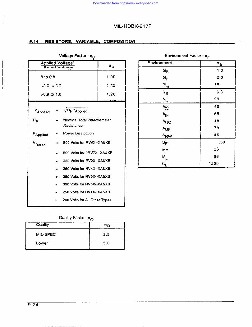
MIL-HDBK-217F
9.14 RESISTORS, VARIABLE, COMPOSITION
Voltage Factor - ~
Applied Voltage*Rated Voltage %
o to 0.8 1.00
>0.8 to 0.9 1.05
>0.9 to 1.0 1.20
“vApplied “ -d
Rp = Nominal Total PotentiometerResistance
‘Applied . Power Dissipation
v Rated = 500 Volts for RV4X--XA8XB
= 500 Vofts for 2RV7X--XA&XB
w 350 Volts for RV2X-XA&XB
= 350 Votts for RV4X--XA&XB
= 350 Votts for RV5X--XA&XB
= 350 Volts for RV6X--XA&XB
w 250 Votts for RV1 X--XA&XB
= 200 Votts for All Other Types
Quality Factor - nO
MIL-SPEC
I Lower
2.5
5.0
Environment Factor - XEEnvironment
GB
GF
GM
N~
Nu
*IC‘IF
‘Uc
*UF
*RW
SF
MF
ML
cl
~E
1.02.0
19
8.0
29
40
65
48
78
46
.50
25
66
1200
9-24
Downloaded from http://www.everyspec.com
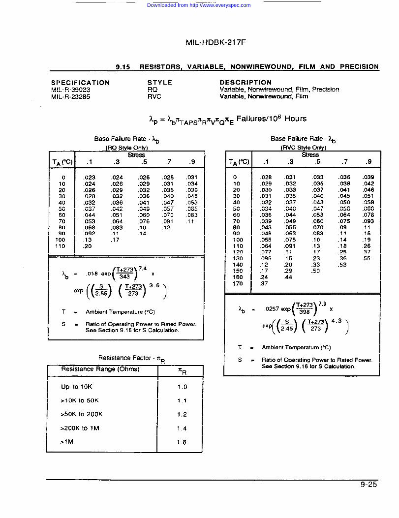
lvllL-t-fDBK-217F
9.15 RESISTORS, VARIABLE, NONWIREWOUND, FILM AND PRECISION
SPECIFICATION STYLE DESCRIPTIONMIL-R-39023 RQ Variable, Nonwirewound, Film, PrecisionMIL-R-23285 RVC Vatiabie, Nonwirewound, Film
Lp = kbXTAp~ZRZvZQnE Failures/l OG Hours
Base Failure Rate - ~~RQ Stvle OnIv)——
&iessTA (W) .1 .3 .5 .7 .9
0 .023 .024 .026 .028 .03110 .024 .026 .029 .031 .03420 .026 .029 .032 .035 .03930 .028 .032 ,036 .040 ,04540 .032 .036 .041 .047 .05350 .037 .042 .049 .057 .065
.044 .051 .060 .070 .083% .053 .064 .076 .091 .1180 .068 .083 .10 .1290 .092 .11 .14100 .13 .17110 .20
()T+273 7.4
h :.,”;;; &F) ‘6 )
T= Ambient Temperature (“C)
s = Ratio of Ogmrating Power to Rated Power.See Section 9.16 for S Calculation.
Resistance Factor - ZR
Resistance Range (Ohms)‘R
Up to 10K 1.0
>1 OK to 50K 1.1
>50K to 200K 1.2
>200K tO 1M 1.4
>lM 1,8I
.
Base Failure Rate - ~lRVP. .Shfk mlu),. . . . -., .- -F !., )
TA (’C) .1 .3 .5 .7 .9
0 .028 .031 .033 .036 .039.029 .032 .035 .038 .042
;; .030 .033 .037 .041 .04630 .031 .035 .040 .045 .05140 .032 .037 .043 .050 .05850 .034 .040 .047 .056 .06660 .036 .044 .053 .064 .07870 .039 .049 .060 .075 .09380 .043 .055 .070 .09 .1190 .048 .063 .083 .11 .15100 .055 .075 .10 .14 .19110 .064 .091 .13 .18 ,26120 .077 .11 .17 .25 .37130 .096 .15 .23 .36 .55140 .12 .20 .33 .53150 .17 .29 .50160 .24 .44170 .37
%= ()T+273 7.9
.0257 exp —398
q(a) (T;Y);3 )
T = Ambient Temperature (“C)
s = Ratio of Operating Power to Rated Power.See Section 9.16 for S Calculation.
9-25
Downloaded from http://www.everyspec.com
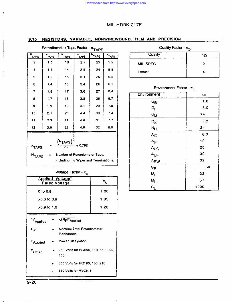
MIL-HDBK-217F
9.15 RESISTORS, VARIABLE, NONWIREWOUND, FILM AND PRECISION
Potentiometer Taps Factor - ~APq. . ..-N N NTAPS ‘TAPS TAPS ‘TAPS TAPS ‘TAPS
3 1.0 73 2.7 23 5.2
4 1.1 14 2.9 24 5.5
5 1.2 15 3.1 25 5.8
6 1.4 16 3.4 26 6.1
7 1.5 17 3.6 27 6.4
8 1.7 18 3.8 28 6.7
9 1.9 19 4.1 29 7.0
10 2.1 20 4.4 30 7.4
11 2.3 21 4.6 31 7.7
12 2.5 22 4.9 32 8.0w
d2
%APS = 25 + 0.792
‘TAPS = Number of Potentiometer Taps,
including the Wiper and Terminations.
Voltage Factor - ~
Applied Voltage”Rated Voltage ‘v
Oto 0.8 1.00
>0.8 to 0,9 1.05
>0.9 to 1.0 1.20
r
●V . ~’Applied
Rp = Nominal Total PotentiometerResistance
‘Applied = Power Dissipation
vRated = 250 Votts for RQ090, 110, 150, 200,
300
= 500 Volts for RQ1 00, 160, 210
a 350 Votts for RVC5, 6
9-26
Quality Factor - TCO
Quality
MIL-SPEC 2
Lower 4
Environment Factor - XE
Environment ~E
GB 1.0
GF 3.0
GM 14
NS 7.0
Nu 24
*IC 6.0
‘IF 12
%c 20
*UF 30
‘RW 39 ISF .50
MF 22
ML 57
c, 1000
Downloaded from http://www.everyspec.com
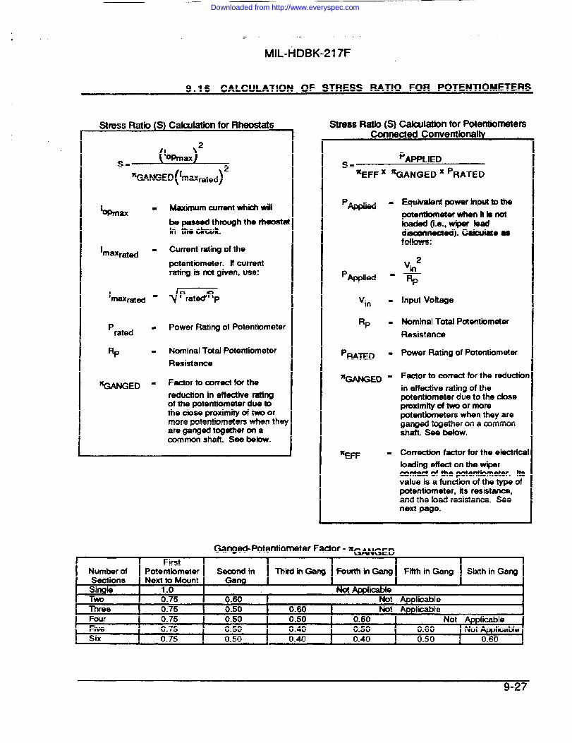
* - ,. “
MIL-HDBK-217F
9.16 CALCULATION OF STRESS RATIO FOR POTENTIOMETERS
Stress Rat& (S) Calculationfor Rheostats
&s- ‘mnax *
%AffiEt)(’maxr~ed)’
ImZIXrat~
Prated
Rp
%ANGED
Maxinwn ament Whii willbe passed through the rheostain tho ckouft.
Current rating of thepotentiometer. H ourrentrating is not given, use:
&te@p
Power Rating of Potentiometer
Nominal TotalPotentiometerResistance
Factor to cxmect for thereduction in affective ratfngof the potentiometer due tothe dose proximity of two ormore potentiometer when theyare ganged together on acwnmon shaft. See bebw.
Stress Ratb (S) Cakulation for PotentiometersConnected Conventionally
‘APPLIEDs.‘EFF x ‘GANGED x ‘RATED
‘Applied
Vin
Rp
%ATED
%4NGED
Equhmkmtpowerinputtothepotendometerwhenitisnotloaded(i.e.,wiper leaddkaommctod).Calcukte asfollows:
V2in%
InputVoltage
Nominal Total PotentiometerResistance
Power Rating of Potentiometer
Factor to correct for the reductionin effective rating of thepotentiometer due to the doseproxim~ uf two or morepotentiometers when they areganged together on a commonshaft. see below.
Correction factor for the electricalloading effect on the wiperoontact of the potentiometer. Itsvalue is a function of the type ofpotentiometer, its resistance,and the bad resistance. Seenext page.
Ganged-Potentiometer FWOf - ICG~GEDFirst
Number of Potentiometer Second in l-hkd in Gang Fourth in Gang Fifth in Gang Sixth in GangSections Next to Mount GangBSingle 1.0 Not App IioableTW 0.75 0.60 ‘ Not ApplicableThree 0.75 0.50 0.60 Not ApplicableFour 0.75 0.50 0.50 0.60 Not ApplicableFive 0.75 0.50 0.40 0,50 0.60 1 Not Applicable
r Six 0.75 I ().50 0.40 I 040 050 I 060
9-27
Downloaded from http://www.everyspec.com
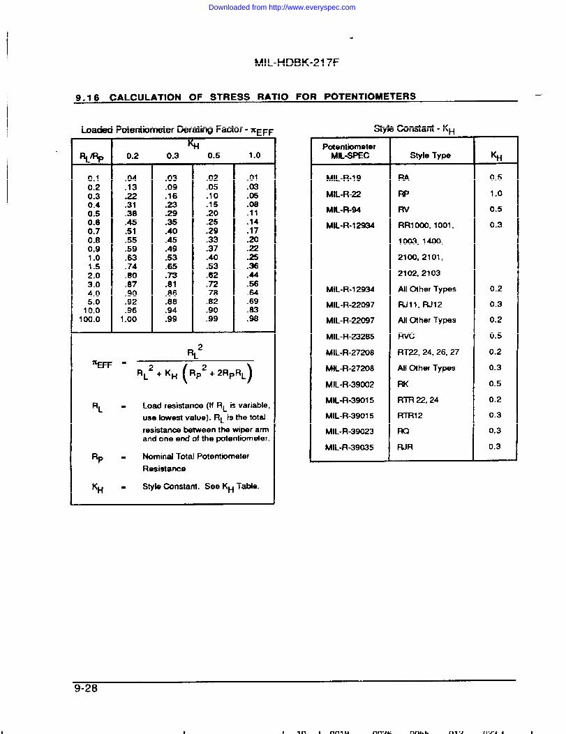
( ,-MIL-HDBK-217F
9.16 CALCULATION OF STRESS RATIO FOR POTENTIOMETERS —
Loaded Potentiometer Derating Factor- ZEFF
0.10.20.30.40.50.60.70.80.91.01.52.03.04.05.010.0100.0
0.2%1
0.3 0.5 1.0
.04
.13
.22
.31
.38
.45
.51
.55
.59
%.80.87.90.92.961.00
.03
.09
.16
.23
.29
.35
.40
.45
.49
.53
.65
.73
.81
.86,88.94.99
.02
.05
.10
.15
.20
.25
.29
.33
.37
.40
.53
.82
.72
.78
.82
.90
.99
.01
.03
.05
.08
.11
.14
.17
%?.25.36.44.56.64.69.83.98
RL2%FF =
(RL2 + KH RP2 + 2RPRL
)
RL = Load resistance (If RL is variable,use lowest value). RL is the totalresistance between the wiper armand one end of the potentiometer.
f%” Nominal Total PotentiometerResistance
%i - Style -nstant. See KH Table.
Styk Constant - KH.,PotentiometerMIL-SPEC Style Type %
MlL-R-l 9 RA 0.5
MIL-R-22 IW 1.0
MN-R-94 Rv 0.5
MlL-R-l 2934 RR1 000, 1001, 0.3
1003, 1400,
2100, 2101,
2102,2103
MIL-R-12934 All Other Types 0.2
MIL-R-22097 RJll, RJ12 0.3
MIL-R-22097 All Other Types 0.2
MIL-R-23285 Rvc 0.5
MIL-R-27208 RT22, 24,26,27 0.2
MIL-R-27208 AHOther Types 0.3
MIL-R-39002 RK 0.5
MIL-R-39015 RTR 22,24 0.2
MJL-R-39015 RTR12 0.3
MIL-R-39023 RQ 0.3
MIL-R-39035 RJR 0.3I
9-28
— ————.--—
Downloaded from http://www.everyspec.com

MIL-HDBK-217F
9.17 RESISTORS, EXAMPLE
Example
Given: Type RVISAYSA505A vartable 500K ohm resistor procured per MIL-R-94, rated at 0.2watts is being used in a fixed ground environment. The resistor ambient temperature is40”C and is dissipating 0.06 watts. The resistance connected to the wiper contact variesbetween 1 megohm and 3 megohms. The potentiometer is connected conventionallywithout ganging.
The appropriate model for RV style variable resistors Is given in Sectbn 9.14. Based on the giveninfon’natbn the folbwing modei factors are determined fnm the tables shown in Seotbn 9.14 and byfoiiowingthe procedure for determining electrical stress for potentiometers as desdbed in Section 9.16.
From Section 9.16
‘APPLIED‘EFF
%ANGED
‘RATED
s
From Section 9.14
.06W
.62 KH . .5 for MIL-R-94 (Section 9.16 Tabie)1.0 Not Ganged (Section 9.16 Table, Single Section,
First Potentbmeter).2W
‘APPLIED .06~EFF x ‘GANGED x ‘RATED = (.62)(1.0)(.2) = ‘m
.047 TA = 40°C, S Rounded to .51.4 500K ohms1.0 3 Taps, Basic Single Potentiometer1.0 VRATED = 250 VOttS for RV1 prefu
VAPPLIED = ~ (500,000)(.06) ~ 173 VOftS173
‘APPLJE#RATED = ~ = ●W2.52.0
% ‘TAPS% ‘V ‘Q ‘E
(.047)(1.0)(1 .4)(1 .0)(2.5) (2.0) = .33 Failures/l 06 Hours
9-29
——
Downloaded from http://www.everyspec.com
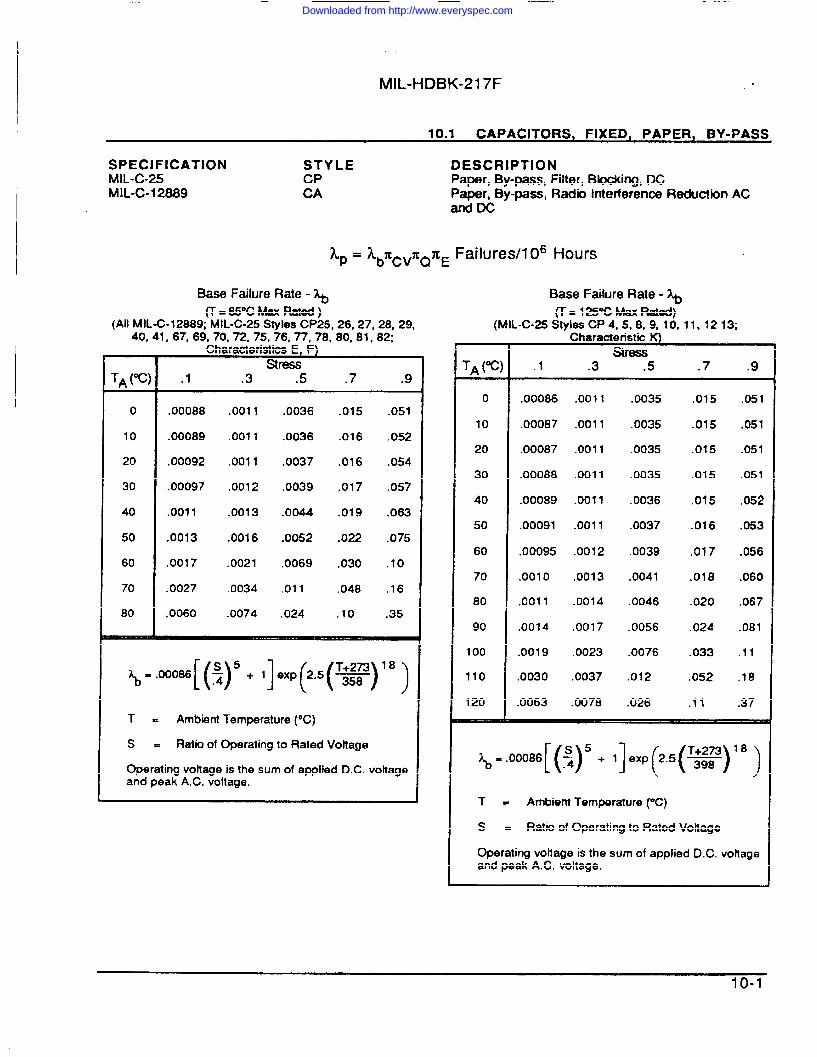
MIL-HDBK-217F .
10.1 CAPACITORS, FIXED, PAPER, BY-PASS
SPECIFICATION STYLE DESCRIPTIONMII--C-25 CP Paper, By-pass, Filter, Blocking, DCMIL-C-12889 CA Paper, By-pass, Radio Interference Reduction AC
andl3--
Zp = lbZCVXQnE Failures/l OG Hours
Base Failure Rate - ~(T.85”c MaxRated)
(All MIL-G-12889:”MIL-C-25 Stvles CP25. 26.27.28.29.40, 41, 67, 69,70,72, 75, 76,77,78:80:81 i 82: ‘
Characteristics E. F)S&
TA (%) .1 .3 .5 .7 .9
0 .00088 .0011 .0036 .015 .051
10 .00089 .0011 .0036 .016 .052
20 .00092 .0011 .0037 .016 .054
30 .00097 .0012 .0039 .017 .057
40 .0011 .0013 .0044 .019 .063
50 .0013 .0016 .0052 .022 .075
60 .0017 .0021 .0069 .030 .10
70 .0027 .0034 .011 .048 .16
80 .0060 .0074 .024 .10 .35
\=.00086[(~)5+ l]exp(2.5(~)18)
T= Ambient Temperature (“C)
s = Ratio of Operating to Rated Voltage
Operating vottage is the sum of applied D.C. vottageand peak A.C. voltage.
Base Failure Rate - ~(T-125% Max Ra!ed)
(MIL-C-25 Styles CP 4,5,8,9, 10, 11, 12 13;
TA (%]
o
10
20
30
40
50
60
70
80
90
100
110
120
Characteristic K)stress
.1 .3 .5 .7 .9
.00086
.00087
.00087
.00088
.00089
.00091
.00095
.0010
.0011
.0014
.0019
.0030
.0063
.0011
.0011
.0011
.0011
.0011
.0011
.0012
.0013
.0014
.0017
.0023
.0037
.0078
.0035
.0035
.0035
.0035
.0036
.0037
.0039
.0041
,0046
.0056
.0076
.012
.026
.015
.015
.015
.015
.015
.016
.017
.018
.020
.024
.033
.052
.11
.051
.051
.051
.051
,052
.053
.056
.060
.067
.081
.11
.18
.37
~=.ooW3[(5)5+1]-p(2..(~)’8)T. Ambient Temperature (“C)
s - Ratio of Operating to Rated Vottage
Operating voftage is the sum of applied D.C. voltageand peak A.C. voltage. I
1o-1
Downloaded from http://www.everyspec.com
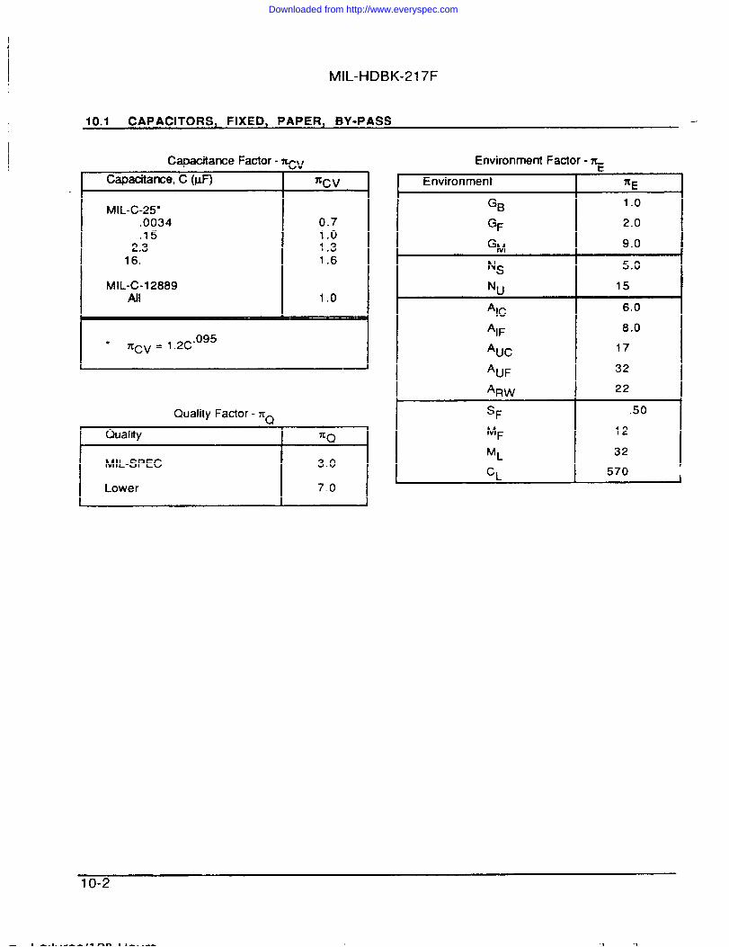
MIL-HDBK-217F
10.1 CAPACITORS, FIXED, PAPER, BY-PASS
Capacitance Factor- WV-.Capacitance, C (@) ‘c v
MIL-C-25*.0034 0.7.15 1.0
2.3 1.316. 1.6
MIL-C-12889All 1.0
●
‘Cv = 1.2c”095
Quality Factor - Xfi
Quality
MIL-SPEC 3.0
Lower 7.0
Environment Factor - x_
Environment
e~
GF
GM
Nu
‘Ic
‘IF
*UC
*UF
%wSF
MF
ML
CL
tfiE
1.02.0
9.0
5.0
15
6.0
8.0
17
32
22
.50
12
32
570
10-2
Downloaded from http://www.everyspec.com
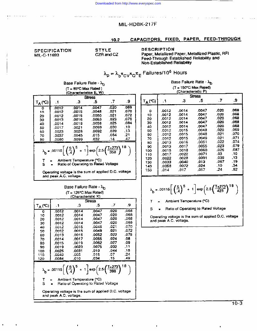
+.- - ., . ... .,. . . . .... . ... .. . ., .,. ,,, . .. ... . .
MIL-HDBK-217F
.10.2 CAPACITORS, FIXED, PAPER, FEED-THROUGH
SPECIFICATION STYLE DESCRIPTIONMlL-C-l 1693 CZR and CZ Paper, Metallizecf Paper, Metallized Plastiq RFI
Feed-Throuqh Established Reliability and
TA (“C)o
;;304050607080 4
Non-Establi;ht?dReliability
Xp = kbZCvZQzE Failures/l 06 Hours
Base Failure Rate - ~(T=85”c MaxRated)(Char-enstics E,W) (
.1 .3 .5 .7 .9.0012 .0014 .0047 .020 .069.0012 .0015 .0048 .021 .070,0012 .0015 .0050 .021 .072.0013 .0016 .0053 .023 .076.0014 .0018 .0058 .025 .084.0017 .0021 .0069 .030 .10.0023 .0028 .0092 .039 .13.0037 .0045 .015 .064 .21.0080 .0099 .032 .14 .47
~=.o.11,[(~)’+1]..P(2.,(~)18)T= Ambient Temperature (“C)s= Ratio of Operating to Rated Voltage
Operating voltage is the sum of applied D.C. voltageand peak A.C. voltage.
TA (“C)o
;:3040
E708090100110120
Base Failure Rate - ~(T= 125°C Max Rated)(Characteristic K)
Sfmss.1 .3 .5 .7 .9.0012 .0014 .0047 .020 .068.0012 .0014 .0047 .020 .068.0012 ,0014 .0047 .020 .068.0012 .0014 ,0047 .020 .069.0012 .0015 .0048 .021 .070.0012 .0015 .0049 .021 .072.0013 .0016 .0052 .022 .075.0014 .0017 .0055 .024 .08.0015 .0019 .0062 .027 .09.0019 .0023 .0075 .032 .11.0025 .0031 .010 .044 .15.0040 .005 .016 .07 .24.0084 .010 .034 .15 .49
\=.00115[(~)’ + l]w(25(Tjfl)18)
T. Ambient Temperature (“C)s = Ratio of Operating to Rated Voftage
Operating vottage is the sum of applied D.C. voltageand peak A.C. voltage.
Base Failure Rate - ~~= 150”C Max Rated)
i~haraeinrktic P},-, ,-, ----- .. ... . f
TA (%) .1 .3 .5 .7 .9
0 .0012 .0014 .0047 .020 .068.0012 .0014 .0047 .020 .068
E .0012 .0014 .0047 .020 .06830 .0012 .0014 .0047 .020 .06840 .0012 .0014 .0047 .020 .06850 .0012 .0015 .0048 .020 .06960 .0012 .0015 .0048 .021 .07070 .0012 .0015 .0049 .021 .07180 .0013 .0016 .0051 .022 .07490 .0013 .0017 .0055 .023 .079100 .0015 .0018 .0060 ,026 .087110 .0017 .0022 .0071 .03 .10120 .0022 .0028 .0091 .039 .13130 .0033 .0040 .013 .057 .19140 .0058 .0072 .024 .10 .34150 .014 .017 .057 .24 .62
~“00115[(~)5+ 1 1 e x p F 5 ( - YT= Ambient Temperature (“C)
s = Ratio of Operating to Rated Vottage
Operating voltage is the sum of applied D.C. vottageand peak A,C. voltage.
I I
Downloaded from http://www.everyspec.com
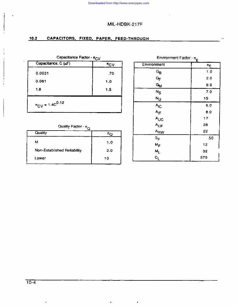
I
i
.
MIL-HDBK-217F
10.2 CAPACITORS, FIXED, PAPER, FEED-THROUGH
Capadtance Factor-WVCapacitance, C (JAF)
0.0031
0.061
1.8
f
I ‘c v = 1.4c0”’2
L.70
1.0
1.5
Quality Factor - XQ
Quality
M
Non-Established Reliability
Lower
1.0
3.0
10
Environment Factor - XE
Environment
GBGF
GMN~
Nu
*IC‘IF
*UC
*UF
%wSF
MF
ML
c,
1.0
2.0
9.0
7.0
15
6,0
8.0
17
28
22
.50
1232
4
10-4
I
Downloaded from http://www.everyspec.com
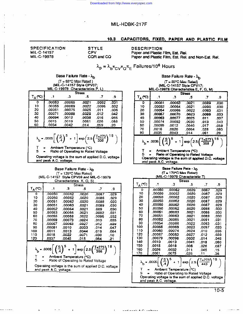
.MIL-HDBK-217F
10.3 CAPACITORS, FIXED, PAPER AND PLASTIC FILM
SPECIFICATION STYLE DESCRIPTIONMIL-C-14157 CPV Paper and Plastk Film, Est. Rel.MIL-C-19978 “ CQR and C(2 Paper and Plastk Film, Est. Rel. and Non-Est. Ret.
1P = &cVZQnE Failures/l Oe Hours
Base Failure Rate - ~(?-=65”c MaxRated)
(MIL-C-14157styleCPV07;MlL-C-l9978 Characteristics P, L]
stressTA ~) .1 .3 .5 .7 .9
0 .00053 .00065 .0021 .0092 .031.00055 .00069 .0022 .0096 .032
;: .00061 .00075 .0025 .011 .03630 .00071 .00088 .0029 .012 .04240 .00094 .0012 ,0038 .016 .05550 .0015 .0019 .0061 .026 .08860 .0034 .0042 .014 .059 .20
~=..oo,[(~)’+1].xp(2..(~)18)T- Ambient Temperature (“C)s- Ratio of Operating to Rated VoftageOperating voltage is the sum of applied D.C. vottageand pa ak A.C. voltage.
Base Faibre Rate - ~(T. 125oCMaxRated)
(MIL-C-141 57 StVta CPV09 and MlL-C-l 9978
TA (“C)o1020304050
%8090100110120
Chara&teristics K, Q, S)Stress
.1 .3 .5 .7 .9.00050 .00062 .0020 .0087 .029.00050 .00062 .0020 .0088 .029.00051 .00062 .0020 .0088 .030.00051 .00063 .0021 .0089 .030.00052 .00064 .0021 .009 .030.00053 .00066 .0021 .0092 .031.00055 .00068 .0022 .0096 .032.00059 .00073 .0024 .010 .035.00067 ,00083 .0027 .012 .039.00081 .0010 .0033 .014 .047.0011 .0013 .0044 .019 .064.0018 .0022 .0071 .030 .10.0037 .0045 .015 .064 .21
~-.ooW[(~)5+l]e.p(2.5(*)’8)T= Ambient Temperature (“C)s. Ratio of Operating to Rated VottageOperating voltage is the sum of applied D.C. voftageand peak A.C. voltage.
Base Failure Rate - ~(-r. e5’’chk Ratacf)
ML-C-14157 StvleCPV17:MIL@--19978 Characteristics E, F; G, M)
St?ess.1 .3 .5 .7 .9
.00051 .00063 .0021 .0089 .030
.00052 .00064 .0021 .0090 .030
.00054 .00066 .0022 .0093 .031
.00057 .00070 .0023 .0099 .033
.00063 .00077 .0025 .011 .037
.00074 .00092 .0030 .013 .043
.00099 .0012 .0040 .017 .058
.0016 .0020 .0064 .028 .093
.0035 .0043 .014 .061 .20
~-.wm[(~)s+l]e.p(2.5(*)18)T- Ambient Temperature (°C)s - Ratio of Operating to Rated VoltageOperating voltage is the sum of appiied D.C. voftageand peak A.C. voltage.
‘A (%)o
Y3040
::
::90100110120130140150160170
Base Failure Rate - ~(T= 170”C Max Rated)
(MIL-C-1 9978 Characteristic T)Stress
.1 .3 .5 .7 .9.00050 .00062 .0020 ,0087 .029.00050 .00062 .0020 .0087 .029.00050 .00062 ,0020 .0087 .029.00050 .00062 .0020 .0087 .029.00050 .00062 .0020 .0087 .029.00050 .00062 .0020 .0088 .030.00051 .00063 .0021 .0088 .030.00051 .00063 .0021 .0089 .030.00052 .00065 .0021 .0091 .031.00054 .00066 .0022 .0093 .031.00056 .00069 .0023 .0097 .033.00060 .00074 .0024 .010 .035.00067 .00083 .0027 .012 .039.00079 .00098 .0032 .014 .046.0010 .0013 .0041 .018 .060.0015 .0018 .006 .026 .087.0026 .0032 .011 .046 .15.0061 .0075 .025 .11 .36
~=.0005[(~)5+ 1].xp(2.5(*)18)
T = Ambient Temperature ~C).
s= Ratio of Operating to Rated VoftageOperating vottage is the sum of applied D.C. vottageand Desk A.C. voltaae.
10-5
. .
Downloaded from http://www.everyspec.com
MIL-HDBK-217F
I
10.3 CAPACITORS, FIXED, PAPER AND PLASTIC FILM
-.Capacitance, C @F) *CV
MIL-C-14157: ●
.0017 .70
.027 1.0
.20 7.31.0 1.6
MIL-C-19978: w.00032 .70.033 1.01.0 1.315.0 1.6
●
‘Cv = 1.6C0”13
● “ 7tcv = 1.3C0.077
Quality Factor - nQQuality ~Q
s .03
R .10
P .30
M 1.0
L 3.0
MlL-C-l 9978, Non-Est. Rel. 10
Lower 30
Environment Factor - XE
Environment %E
GB 1.0
GF 2.0
GM 8.0
Ns 5.0
Nu 14
%c 4.0
‘IF 6.0
*UC 11.0
*UF 20
*RW 20
SF .50
MF 11
ML 29
c’ 530
10-6
Downloaded from http://www.everyspec.com
MIL-HDBK-217F
10.4 CAPACITORS, FIXED, METALLIZED PAPER, PAPER-PLASTIC AND PLASTIC
SPECIFICATION STYLE DESCRIPTIONMIL-C-18312 CH Metallized Paper, Paper-Plastic, PlasticMI L-C-39022 CHR MetalJized Paper, Paper-Plastic, Plastic,
Established Reliabifii
kp = kbTCCvXQxE Failures/l OG Hours
Base Failure Rate - ~(T-85”c MaxRated)
(MIL-C-39022Charactertatic9 and 12 (50 Voltsrated].Chara
~ (%)
o
10
20
30
40
50
60
70
80
eristic 49; and MlL-C-l 8312 Characteristic R)”stress
.1 .3 .5 .7 .9
.00070
.00072
.00074
.00078
.00086
.0010
.0014
.0022
.0048
.00087
.00089
.00091
,00097
.0011
.0013
.0017
.0027
.0059
.0029
.0029
.0030
.0032
.0035
.0041
.0055
.0089
.019
.012 .041
.012 .042
.013 .043
.014 .046
.015 .051
.018 .06
.024 .08
.038 .13
.084 .28
~=.WW9[(~)5+ l]exp(2.5 (=)18)
T. Ambient Temperature (“C)
s- Ratio of Operating to Rated Voltage
Operating voftage is the sum of applied D.C. voltageand peak A.C. voltage.
Base Failure Rate - ~(T=1250CMax Rated)
(MIL-C-39022 Char~eristic 9 and 12 (above 50 Vottsratedl Characteristics 1.10, 19, 29, 59; and
TA (~)
o
10
20
30
40
50
60
70
80
90
100
110
120
“.MlL-C-l8312 Chara%istic N)Strass
.1 .3 .5 .7 .9
.00069
.00069
.00070
.00070
.00071
.00073
.00076
.00082
.00092
.0011
.0015
.0024
.0051
.00086
.00086
.00086
.00087
.00088
.00090
.00094
.0010
.0011
.0014
.0019
.0030
,0063
.0028
.0028
.0028
.0028
.0029
.003.
.0031
.0033
.0037
.0045
.0061
.0098
.020
.012
.012
.012
.012
.012
.013
.013
.014
.016
.019
.026
.042
.088
.041
.041
.041
.041
.042
.043
.04s
.048
.054
.065
.088
.14
.30
\=.00069[(~)’+ l]exP(2.5 (=)18)
T= Ambient Temperature (“C)
S = Ratio of Operating to Rated Voltage
Operating voltage is the sum of applied D.C. voltageand peak A.C. voltage.
Downloaded from http://www.everyspec.com
MIL-HDBK-217F
10.4 CAPACITORS, FIXED, METALLIZED PAPER, PAPER-PLASTIC AND PLASTIC
Capadtance Factor- wvCapacitance,C @F) ‘c v0.0029
0.14
2.4
.70
1.0
1.3
0.092Zcv = 1.2C
Quality Factor - Xnu
Quality 7CQ
s 0.03
R .10
P .30
M 1.0
L 3.0
MIL-C-18312, Non-Est. Rel. 7.0
Lower 20
Emkmment Factor -xcb
Environment ~E
GB 1.0
GF 2.0
% 8.0
NS 5.0
Nu 14
*IC 4.0
‘IF 6.0
*UC 11.0
*UF 20
‘RW 20
SF .50
MF 11
ML 29
CL 530
Downloaded from http://www.everyspec.com
MIL-HDBK-217F
10,5 CAPACITORS, FIXED, PLASTIC AND METALLIZED PLASTIC
SPECIFICATION STYLE DESCRIPTIONMIL-C-55514
TA (%)
o
10
20
30
40
50
60
70
80
CFR Plastic, Metallized Plastic, Est. Rel.
Xp = kbXcvXQzE Failures/l OG Hours
(Characteristics M, N’)
.1 .3 .5 .7 .9
.0010
.0010
.0011
.0011
.0012
.0015
,0020
.0032
.0069
.0012
.0013
.0013
.0014
.0015
.0018
.0024
.0039
.0085
.0041
.0042
.0043
.0045
,0050
.0059
.0079
.013
.028
.018
.018
.018
.020
.022
.026
.034
.055
.12
.059
.060
.062
.066
.073
.086
,11
.18
.40
~=.00099[(:)5+ l]exP(2.5 (%)18)
T= Ambient Temperature (“C)
s= Ratio of Operating to Rated Voltage
Operating vottage is the sum of applied C).C. voftageand peak A.C. voltage,
Base Failure Rate - ~(T= 12SOCMaxRated)(Charadari@im 0 R !%)\ -. -------- .-. .— -, , ., - t
StrwsTA (“C) .1 .3 .5 .7 .9
0 .00099 .0012 .0040 .017 .058
10 .0010 .0012 .0040 .017 .058
20 .0010 .0012 .0041 .017 .059
30 .0010 .0012 .0041 .018 .059
40 .0010 .0013 .0041 .018 .060
50 .0011 .0013 .0043 .018 .062
60 .0011 .0014 .0044 .019 .064
70 .0012 .0015 .0048 .020 .069
80 .0013 .0016 .0054 .023 .077
90 .0016 .0020 .0065 .028 .094
100 ,0022 .0027 .0087 .038 .13
110 .0035 .0043 .014 .06 .20
120 .0073 .0090 .029 .13 .43
\=.00099[(;)5+ 1].XP(2.5 (-)18)
T= Ambient Temperature (“C)
s- Ratio of Operating to Rated Voltage
Operating vottage is the sum of applied D.C. voltageand peak A.C. voftage.
i
Downloaded from http://www.everyspec.com
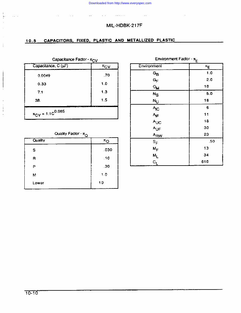
,.. . .
MIL-J+DBK-217F
10.5 CAPACITORS, FIXED, PLASTIC AND METALLIZED PLASTIC
Capacitance Factor- WVCapacitance, C (jLF) I ~cv
0.0049 .70
0.33 1,0
7.1 1.3
38. 1.5
0.0857CCV=1.1 C
Quality Factor - ZQ
Quality ~Q
s .030
R .10
P .30
M 1.0
Lower 10
EnvironmentFactor - n=L
Environment ~E
GB 1.0
GF 2.0
GM 10
Ns 5.0
Nu 16
Alc 6
% 11
%c 18
*UF 30
‘RW 23
SF .50
MF 13
ML 34
cL 610
1o-1o
1 I I ,-- 1 n—I— —--A A.-
Downloaded from http://www.everyspec.com
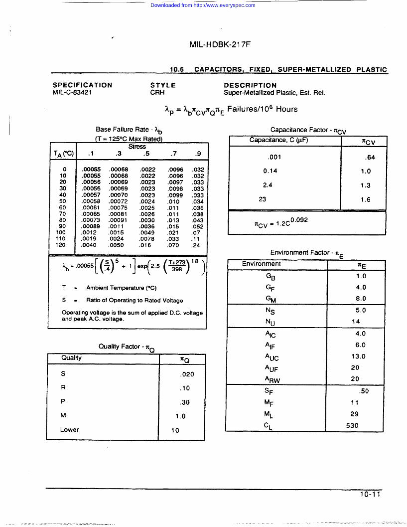
/MIL-HDBK-21 7F
10.6 CAPACITORS, FIXED, SUPER-METALLIZED PLASTIC
SPECIFICATION STYLE DESCRIPTIONMIL-C-63421 CRH Super-Metallized Plastic, Est. Rel.
1P = kbXCvZQnE Failures/l OG Hours
o
::30405060708090100110120
Base Failure Rate - ~(T= 125°C Max Rated)
stress.1 .3 .5 .7 .9
.00055
.00055
.00056
.00056
.00057
.00058
.00061
.00065
.00073
.00089
.0012
.0019
.0040
.00068 ,0022 .0096 .032
.00068 .0022 .0096 .032
.00069 .0023 .0097 .033
.00069 .0023 .0098 .033
.00070 .0023 .0099 .033
.00072 .0024 .010 .034
.00075 .0025 .011 .036
.00081 .0026 .011 .038
.00091 .0030 .013 .043
.0011 .0036 .015 .052,0015 .0049 .021 .07.0024 .0078 .033 .11.0050 .016 .070 .24
~=.00055[(~)5 + 1].XP(2.5 (~)” ;
T. Ambient Temperature (“C)
s= Ratio of Operating to Rated Vottage
Operating voltage is the sum of applied D.C. voltageand peak A.C. voltage.
Quality Factor - ZQ
Quality
sR
P
M
Lower
7tQ
.020
.10
.30
1.0
10
Capacitance Factor - WVt
Capacitance, C (vF) ‘Cv.001 .64
0.14 1.0
2.4 1.3
23 1.6
0.092ncv = 1 .2C
Environment Factor - X_
I Environment
GBGF
GM
Ns
Nu
Alc‘IF
‘Uc
‘UF
fhvsF
MF
ML
CL
4.0
8.0
5.0
14
4.0
6.0
13.0
20
20
.50
11
29
530
. . —. —— ———
Downloaded from http://www.everyspec.com
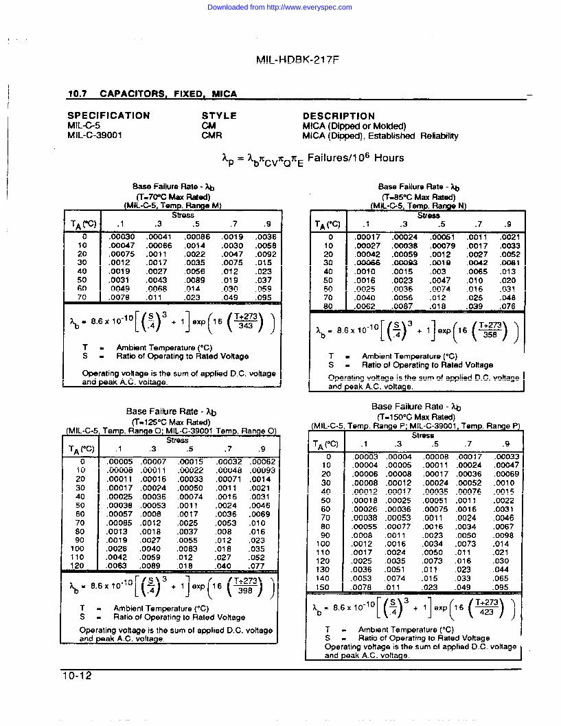
t
MIL-HDBK-217F
10.7 CAPACITORS, FIXED, MICA
SPECIFICATION STYLE DESCRIPTIONMIL-C-5 CM MICA (Dipped or Molded)MIL-C-39001 CMR MICA (Dipped), Established
TA ~)T
10203040506070
Ap = LbZCvZQzE Failures/l OG Hours
BaseFailure Rate - ~(T=70”C Max Rated)
(MIL-G5, Temp. Range M)stress
.1 .3 .5 .7 .9.00030 .00041 .00086 .0019 .0036.00047 .00066 .0014 .0030 .0058.00075 .0011 .0022 .0047 .0092.0012 .0017 .0035 .0075 .015.0019 .0027 .0056 .012 .023.0031 .0043 .0089 .019 .037.0049 .0068 .014 .030 .059.0078 .011 .023 .049 .095
~= 8.6x10⁻¹⁰ [(3)3 + I]exP(16 (~) )
T. Ambient Temperature (“C)s. Ratio of Operating to Rated Voltage
Operating vottage is the sum of applied D.C. voltage
f!fwiTA (“C)
o102030405060708090100110120
Base FailureRate - ~(T=125°CMaxRated)
Temp. Range O; MIL-C-39001 Temp. Ranqe 0)Stress
.1 .3 .5 .7 .9.00005 .00007 .00015 .00032 .00062.00008 .00011 .00022 .00048 .00093.00011 .00016 .00033 .00071 .0014.00017 .00024 .00050 .0011 .0021.00025 .00036 .00074 .0016 .0031.00038 .00053 .0011 .0024 .0046.00057 .0008 .0017 .0036 .0069.00085 .0012 .0025 .0053 .010.0013 .0018 .0037 .008 .016.0019 .0027 .0055 .012 .023.0028 .0040 .0083 .018 .035,0042 .0059 .012 ,027 .052.0063 .0089 .018 .040 .077
~b= 8.6)( 10-10 [(3)3+ jeW(16 (%%))
T= Ambient Temperature (“C)s= Ratio of Operating to Rated VottageOperating voltage is the sum of applied D.C. voltageand pa ak A.C. voltage.
10-12
Reliability
Base Failure Rate - ~(T=850C Max Rated)
(MIL-C-5, Temp. Ran@ N)I stress
TA (“C) .1 .3 .5 .7 .90 .00017 .00024 .00051 .0011 .002110203040506070
.00027 .00038 .00079 .0017 .0033
.00042 .00059 .0012 .0027 .0052
.00066 .Ooow .0010 .0042 .0081
.0010 .0015 .003 .0065 .013
.0016 .0023 .0047 .010 .020
.0025 .0036 .0074 .016 .031
.0040 .0056 .012 .025 .04880 I .0062 .0087 .018 .039 .076
lb= 8.6 XW1O [(~)3+ 1]W(16 (w) )
T= Ambient Temperature (oC)s. Ratio of Operating to Rated VottageOperating voltage is the sum of applied D.C. voltageand peak A.C. voltage.
Base Failure Rate - ~n=1500C Max Rated)
UY!!kQsTemp.R-ange P; MIL-C-39001, Temp. Ranqe P)stress
.1 .3 .5 .7 .9TA (“C)o10203040
%708090100110120130140150
.00003 .00004 .00008 .00017 .00033
.00004
.00006
.00008
.00012
.00018
.00026
.00038
.00055
.0008
.0012
.0017
.0025
.0036
.0053
.00005
.00008
.00012
.00017
.00025
.00036
.00053
.00077
.0011
.0016
.0024
.0035
.0051
.0074
.00011
.00017
.00024
.00035
.00051
.00075
.0011
.0016
.0023
.0034
.0050
.0073
.011
.015
.00024
.00036
.00052
.00076
.0011
.0016
.0024
.0034
.0050
.0073
.011
.016
.023
.033
.00047
.00069
.0010
.0015
.0022
.0031
.0046
.0067
.0098
.014
.021
.030
.044
.065.0078 .011 .023 .049 .095
Ab= S.6XIO-10[(33+ 1].XP(16 (7;;?) )
T= Ambient Temperature (“C)s- Ratio of Operating to Rated VoftaqeOperating voltage is the s~m of applied D.C. voltageand peak A.C. voltage.
Downloaded from http://www.everyspec.com
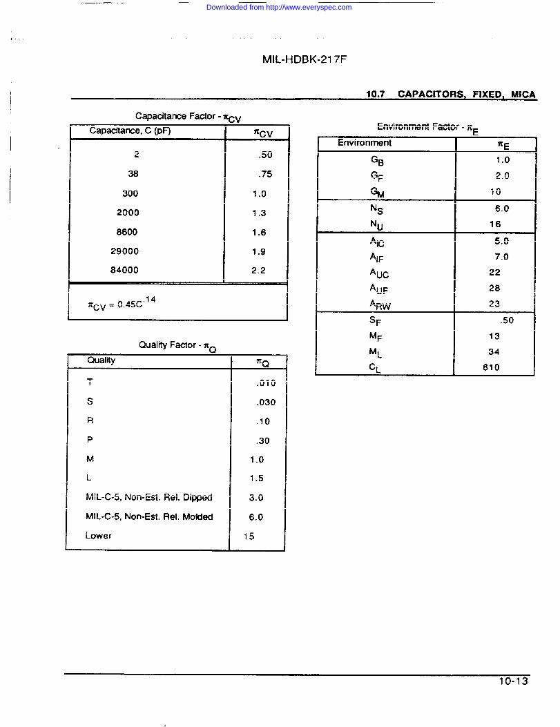
* ,.
MIL-HDBK-217F
10.7 CAPACITORS, FIXED, MICA
Capacitance Factor - ~VCapacitance,C (pF)
2
38
300
2000
8600
29000
84000
I ‘Cv = 0.45C”4
‘Cv
.50
.75
1.0
1.3
106
1,9
2.2
Quality Factor - nQQuality
T
sR
P
M
L
MIL-C-5, Non-Est. Rel. Dipped
MIL-C-5, Non-Est. Ref. Molded
Lower
.010
.030
.10
.30
1.0
1.5
3.0
6.0
15
EnvironmentFactor - z=Environment
GB
GF
%Ns
Nu
%c
‘IF
‘Uc‘UF
%nNSF
MF
ML
c1
1.0
2.0
10
6.0
16
5.0
7.0
22
28
23
.50
13
34
610
10-13
n r - -- ...:-- r--- ---- L nu.
Downloaded from http://www.everyspec.com
MIL-HDBK-217F
10.8 CAPACITORS, FIXED, MICA, BUTTON —
SPECIFICATION STYLE DESCRIPTIONMIL-C-1095O CB MICA, Button Style
Xp = LbZCvXQnE Failures/l OG Hours
Base Failure Rate - ~(T= 85°C Max Rated)
(Stvle CB50)‘s&-
TA (Z) .1 .3 .5 .7 .9
0 .0067 .0094 .019 ,042 .082
10 .0071 .0099 .021 .044 .086
20 .0076 .011 .022 .047 .092
30 .0082 .011 .024 .051 .10
40 .009 .013 .026 .056 .11
50 .010 .014 .029 .063 .12
60 .012 .016 .033 .072 .14
70 .013 .019 .039 .084 .16
::00 5~~~~)~~l]ex~72 (~-
T. Ambient Temperature (“C)
s= Ratio of Operating to Rated Voltage
Operating vottage is the sum of applied D.C. voltageand peak A.C. voltage.
Base Failure Rate - ~(T= 150”C Max Rated)fAll TvoP= Fxrxmt CR50\\. ....- ------ ----- 1
stressTA (“C) .1 .3 .5 .7 .9
0 .0058 .0081 .017 .036 .071
10 .0059 .0083 .017 .037 .072
20 .0061 .0085 .018 .038 .074
30 .0062 .0087 .018 .039 .076
40 .0064 .009 .019 .040 .079
50 .0067 .0094 .019 .042 .082
60 .0070 .0098 .020 .044 .086
70 .0074 .010 .022 .046 .090
80 .0079 .011 .023 .049 .096
90 .0085 .012 .025 .053 .10
100 .0093 .013 .027 .058 .11
110 .010 .014 .03 .064 .12
120 .011 .016 .033 .072 .14
130 .013 .018 .038 .082 .16
140 .015 .021 .044 ,095 .18
150 .018 .025 .052 .11 .22k i
~= .0053 [(~)3 + l]exP(l.2 (T~~~)63)
T= Ambient Temperature (°C)
s== Ratio of Operating to Rated Voftage
Operating voltage is the sum of applied D.C. voltageand peak A.C. voltage. c
10-14
Downloaded from http://www.everyspec.com
*
MIL-HDBK-217F
10.8 CAPACITORS, FIXED, MICA, BUTTON
Quality Factor - ZQQuality ftQ
MIL-C-1095O
Lower
5.0
15
Capacitance Factor - ~vCapacitance,C (pF)
8
50
160
500
1200
2600
5000
‘Cv = .31c0”23
‘Cv
.50
.76
1.0
1.3
1.6
1.9
2.2
Environment Factor - X.h
Environment,GBGF
GMNsNukAC
‘IF*UC
‘UF‘RWSFMFMLcL
t
1.0
2.0
10
5.0
16
5.0
7.0
22
28
23
.50
13
34
610
10-15
. =——n—-—-—==—-=-—c=.=—=——s—-———————ee—..- - _m_—- . . . . . _._.._.~==_.
Downloaded from http://www.everyspec.com
MIL-HDBK-217F
III, 10.9 CAPACITORS, FIXED, GLASS —I
SPECIFICATION STYLE DESCRIPTIONMlL-C-l 1272 CY GIass
I MIL-C-23269 CYR Glass, Established Reliability
WL!!!!!TA (%;
o
10
20
30
40
50
60
70
80
90
100
110
120
Ap = kbnCVTCQnE Failures/l OG Hours
Base FaitureRate - ~(T=125°C Max Rated)
C-23296 and MlL-C-l 1272 Temp. Range ClStm’ss
.1 .3 .5 .7 .9
.00005
.00007
.00011
.00016
.00024
.00036
.00054
.0008
.0012
.0018
.0027
.0040
.0060
.00005
.00008
.00012
.00018
.00027
.00041
.00061
.00091
.0014
.0020
.0030
.0045
.0068
.00010
.00014
.00022
.00032
.00048
.00072
.0011
.0016
.0024
.0036
.0054
.0080
.012
.00023
.00035
.00052
.00078
.0012
.0017
.0026
.0039
,0058
.0087
.013
.019
.029
.0005!
.0008
.0012
.0018
.0028
.0041
.0062
.0092
.014
.021
.031
.046
.069
‘b = 8.25X lo-fo [(:)4 + 1].xlp (T;%) )
T= Ambient Temperature (“C)
s= Ratio of Operating to Rated Vottage
Operating voltage is the sum of applied D.C. vottageand peak A.C. voltage.
TA (“C
o102030405060708090100110120130140150160170
180190200
Base Failure Rate - &(T= 200°C Max Rated)
(MIL-C-11272 Ternp Range D)&
.1 .3 .5 .? .9
.00001
.00001
.00002
.00002
.00003
.00005
.00006
.00009
.00013
.00018
.00025
.00035
.00049
.00069
.00096
.0014
.0019
.0027
.0037
.0052
.0073
.Oooo1
.00001
.00002
.00003
.00004
.00005
.00007
.00010
.00014
.00020
.00028
.00039
.00055
.00078
.0011
.0015
.0021
.0030
.0042
.0059
.0083
.00002
.00002
.00003
.00005
.00007
.00009
.00013
.00018
.00025
.00035
.00050
.00070
.00098
.0014
.0019
.0027
.0038
.0053
.0075
.010
.015
.00004
.00006
.00008
.00011
.00016,00022.00031.00044.00061.00086.0012.0017.0024.0033.0047.0065.0092.013
.018
.025,035
.00010
.00014
.00019
.00027
.00038
.00053
.00074
.0010
.0015.0020.0029.0040.0056.0079.011.016.022.031
.043
.060,084
$= 8.25x I0 -q(:)4+ 1]W(16 (%%) )
T= Ambient Temperature (“C)
s. Ratio of Operating to Rated Voltage
Operating voltage is the sum of applied D.C, voltageand peak A.C. voltage.
Downloaded from http://www.everyspec.com
Ml13HDBK-217F
10.9 CAPACITORS, FIXED, GLASS
Capacitance Factor- ~,v-.Capacitance,C (pF) ‘Cv
1 .62
4 .75
30 1.0
200 1.3
900 1.6
3000 1.9
8500 2.2
‘Cv = 0.62C0”14
Quality Factor- ~Q
Quality ~Q
s .030
R .10
P .30
M 1.0
L 3.0
MlL-C-l 1272, Non-Est. Rel. 3.0
Lower 10
Environment Factor - ZEEnvironment ~E
GB 1.0
GF 2.0GM 10
Ns 6.0Nu 16
AC 5.0
‘IF 7.0
*UC 22
*UF 28
‘RW 23
SF .50MF 13ML 34CL 610
10-17
Downloaded from http://www.everyspec.com
MJL-HDBK-21
10.10 CAPACITORS, FIXED, CERAMIC, GENERAL
sMM
I
7F
PURPOSE —
3ECIFICATION STYLE DESCRIPTION!L-C-11015 GK Ceramk, General PuqxxeL-C-39014 CKR Ceramk, General Purpose, Est. Rel.
Lp = kbZcvZQnE Failures/l OG Hours
o10
L20304050607080.
Base Failure Rate - ~(T= 850C Max Rated)
AIL-C31014 Styles CKR13, 48, 64, 72;IL-C-I 1015 Type A Rated Temperature)
.1 .3 .5 .7 .9.00067 .0013 .0036 .0088 .018.00069 .0013 .0037 .0091 .019.00071 .0014 .0030 .0093 .019.00073 .0014 .0039 .0096 .020.00075 .0014 .004 .0099 .020.00077 .0015 .0042 .010 .021.00079 ,0015 .0043 ,010 .021.00081 .0016 .0044 .011 .022.00083 .0016 .0045 .011 .023
%- 0003[(33“ 1 8X ’ ( T =)T= Ambient Temperature (“C)s= Ratio of Operating to Rated VoltageOperating vottage is the sum of applied D.C. voltageand peak A,C. voltage.
Base Failure Rate - ~(T= 125°C Max Rated)
(MIL-C-39014 Styles CKR05-12, 14-19, 73, 74;
‘A (=)o10
::405060708090100110120
IL-C- I 1015 Type B Rated Temperature)stress
.1 .3 .5 .7 .9.00062 .0012 .0033 .0082 .017.00063 .0012 .0034 .0084 .017.00065 .0013 .0035 .0086 .018.00067 .0013 .0036 .0088 .018.00068 .0013 .0037 .0090 .018.00070 .0014 .0038 .0093 .019.00072 .0014 .0039 .0095 .019.00074 .0014 .0040 .0097 .020.00076 .0015 .0041 .010 .020.00077 .0015 .0042 .010 .021.00079 .0015 .0043 .010 .021.00081 .0016 .0044 .011 .022.00084 .0016 .0045 .011 .023
.‘b = ooo’[(~)’+11“p(=)T= Ambient Temperature (“C)s. Ratio of Operating to Rated VoltageOperating voltage is the sum of applied D.C. vottageand peak A.C. voltage.
TA (W
o
10
20
30
40
50
60
70
80
90
100
110
120
130
140
150
Base Failure Rate - ~(T =1500C Max Rated)
ItL-C-l 1015 Type C Rated Temperature)
.1 .3 .5 .7 .9
.00059
.00061
.00062
.00064
.00065
.00067
.00068
.00070
.00072
.00073
.00075
.00077
.00079
.00081
.00083
.00085
.0011
.0012
.0012
.0012
.0013
.0013
.0013
.0013
.0014
.0014
.0014
.0015
.0015
.0016
.0016
.0016
.0032
.0033
.0034
.0035
.0035
.0036
.0037
.0038
.0039
.0040
.0041
.0042
.0043
.0044
.0045
.0046
.0078
.00’8
.0082
.0084
.0086
.0088
.009
.0092
.0095
.0097
.0099
.010
.010
.011
.011
.011
.016
.016
.017
.017
.018
.018
.018
.015
.019
.020
.020
.021
.021
.022
.022
.023
\ - 0 0 0 3 [ ( 3 3 + 1 1 ‘ x pT- Ambient Temperature (“C)
s. Ratio of Operating to Rated Vottage
Operating vottage is the sum of applied D.C. voltageand peak A.C. voltage.
NOTE: The rated temperature designation (type A,B, or C) is shown in the pan number, e.g.,CKG1AW22M).
Downloaded from http://www.everyspec.com
MIL-HDBK-217F
I 10.10 CAPACITORS, FIXED, CERAMIC, GENERAL PURPOSE
Capacitance Factor - WVCapacitance, C (pF)
6.0
240
3300
36,000
240,000
1,100,000
4,300,000
I 0.11Xcv = .41C
~cv.50
.75
1.0
1.3
1.6
1.9
2.2
QualityQuality Factor - n=
sR
P
M
L
MlL-C-l 1015, Non-Est. Rel.
Lower
.030
.10
.30
1.0
3.0
3.0
10
EnvironmentFactor - n=Environment
GB
GF
GM
Ns
Nu
Ac
‘IF
‘Uc*UF
*RWSF
MF
ML
c1
L
1.0
2.0
9.0
5.0
15
4.0
4.0
8.0
12
20
.40
13
34
610
4.
10-19
Downloaded from http://www.everyspec.com
MIL-I-IDBK-217F
10.11 CAPACITORS, FIXED, CERAMIC, TEMPERATURE COMPENSATING AND CHIP –
SPECIFICATION STYLE DESCRIPTIONMIL-C-20 CCR and CC Ceramic, Temperature Compensating, Est.
and Non Est. Rel.MIL-C-55681 CDR Ceramic, Chip, Est. Rel.
IBase Failure Rate - ~
(MIL-C
~~ W)
10203040
E7080
lp = kbZcVXOzE Failures/l OG Hours
Capacitance Factor - ~,v(r-85% Max Ratecf)
) StybsCC 20,25,30,32,35, 45, 85, 95-97)Stress
.1 .3 .5 .7 .9.00015 .00028 .00080 .0019 .0040.00022 .00042 .0012 ,0029 .0059.00033 .00063 .0018 .0043 .0088.00049 .000!34 .0026 .0064 .013.00073 .0014 .0039 .0096 .020.0011 .0021 .0059 .014 .029.0016 .0031 .0088 .021 .044.0024 .0046 .013 .032 .065.0036 .0069 .019 .047 .097
\ = 2.6x1O -9[(:)3+ 1].XP(14.3 (T;3 ) )1
T. Ambmnt Temperature (%)s- Ratio of Operating to Rated VoltageOperating vottage is the sum of applied D.C. vottageand maak A.C. vottaoe.
Base Failure Rate - ~(T= 125oC Max Rated)
(MIL-C-20 Styles CC 5-9,13-19,21,22,26,27, 31,33,36, 37, 47, 50-57, 75-79, 81-83, CCR 05-09,13-19, 54-57, 75-79, 81-83, 90; MIL-C-55681 All CDR Styles)
StressTA (“C) .1 .3 .5 .7 .9
0 .00005 .00009 .00027 .00065 .0013.00007 .00014 .00038 .00093 .0019
E .00010 .00019 .00055 .0013 .002730 .00014 .00028 .00078 .0019 .003940 .00021 .00040 .0011 .0027 .005650 .00030 .00057 .0016 .0039 .00860 .00042 .00082 .0023 .0056 .01170 .00061 .0012 .0033 .008 .01680 .00087 .0017 .0047 ,011 .02390 .0012 .0024 .0068 .016 .034100 .0018 .0034 .0097 .024 .048110 .0026 .0049 .014 .034 .069120 1 .0037 .0071 .020 ,048 .099
~= 2.6x10 ‘g[(~)’+ l]exp(143 (TJ~T ) )
T= Ambient Temperature (“C)s. Ratio of Operating to Rated VoltageOperating vottage is the sum of applied D.C. voftageand peak A.C. voltage.
Capacitance, C (pF) ‘CvL1 .597 .75
81 1.0720 1.3
4,100 1.6I 17,000 I 1.9 I
58;000 I 2.2 I0.12Zcv = .59C
, \
Quality Factor - XQQuality ~Q 4s .030R .10P .30M 1.0Non-Est. Rel. 3.0Lower 10
Environment Factor - XE
I Environment I ~EI
GB 1.0
GF 2.0
% 10
N~ 5.0
Nu 17
%c 4.0
‘IF 8.0
*UC 16
1
*UF 35
*RW 24
SF .50
MF 13
ML 34
I I 610 II0-20
Downloaded from http://www.everyspec.com

MIL-HDBK-217F
10.12 CAPACITORS, FIXED, ELECTROLYTIC, TANTALUM, SOLID
SPECIFICATION STYLE DESCRIPTIONMIL-C-39003 CSR Tantatum Electrolytic (Solid), Est. Ret.
z n Failures/l OG Hours‘P = %mCV%R Q E
~ (“c)o102030405060708090100110120
Base Failure Rate - ~Stress
.1 .3 .5 .7 .9.0042 .0058 .012 .026 .051.0043 .0060 .012 .027 .052.0045 .0063 .013 .028 .055.0048 .0067 .014 .030 .058.0051 .0072 .015 .032 .0’63.0057 .0079 .016 .035 .069.0064 .009 .019 .040 .078.0075 .011 .022 .047 .092.0092 .013 .027 .050 .11.012 .017 .034 .074 .14.016 .023 .047 .10.024 .034 .07 .15.039 .054 .11 .24
Lb = .00375 [(~)3 . 1]..p(2.6 (T~& ) ‘ )
T. Ambient Temperature (“C)s= Ratio of Operating to Rated Vottageoperating votiage is the sum of applied D.C. vohageand peak A.C. voltage.
Capacitance Factor - WVCapacitance, C @F) ‘Cv
.003 0.5
.091 .751.0 1.08.9 1.350 1.6
210 1.9710
0.12n~v = 1 .Oc
Quality Faotor-x.u
●
QualityDcsBRPMLLower
+%-I0.0100.0300.0300.100.301.01.5
10
Series Resistance Factor - ZslCircuit Resistance, CR (ohms/vott)
>0.8
>0.6 to 0.8
>0.4 to 0.6
>0.2 to 0.4
>0.1 to 0.2
0 to 0.1
% R
.066
.10
.13
.20
.27
.33
CR = Eff. Res. Between Cap. and Pwr. SupplyVoltage Appiied to Capacitor
Envimment Factor - YC=L
Environment
GBGF
%NS
Nu
AC
‘IF*UC
*UF‘RWSFMFMLCL
1.0
2.0
8.0
5.0
14
4.0
5.0
12
20
24
.40
11
29
530
Downloaded from http://www.everyspec.com
MIL-HDBK-217F
10.13 CAPACITORS, FIXED, ELECTROLYTIC, TANTALUM, NON-SOLID
SPECIFICATION STYLE DESCfMIL-C-3965 CL TantalwMIL-C-39006 CLR Tantalw
IPTION1, Electr’olyk (Non-Solid)I, Electrolytic (Non-Solid), Est. Rel.
kp = kbXcVZCXQxE Failures/l 06 Hours
Base Failure Rate - ~(-r = 85°C Max Rated)
(MIL-C-3965 Styles CL24-27, 34-37)stress
TA (“C) .1 .3 .5 .7 .90 .0021 .0029 .0061 .013 .02610 .0023 .0032 .0067 .014 .02820 .0026 .0036 .0075 .016 .03130 .0030 .0042 .0087 .019 .03640 .0036 .0051 .011 .023 .04450 .0047 .0066 .014 .029 .05760 .0065 .0091 .019 .041 .079
~~ool~
T = Ambient Temperature (“C)s. Ratio of Operating to Rated VoltageOperating voltage is the sum of applied D.C. voltageand peak A.C. voltage.
Base Failure Rate - ~(T= 125°C Max Rated)
(MIL-C-3965 Styles CL20-23, 30-33, 40-43, 46-56, 64-
TA (“C)o102030405060708090100110120
i7, 70-73; and all MI L-C-39006 Styles)Stress
,1 .3 .5 .7 .9
.0018 .0026 .0053 .011 .022
.0019 .0026 .0055 .012 .023
.0020 .0028 .0057 .012 .024
.0021 .0029 .0061 .013 .026
.0023 .0032 .0066 .014 .028
.0025 .0035 .0072 .016 .030
.0028 .0040 .0082 .018 .034
.0033 .0046 .0096 .021 .040
.0041 .0057 .012 .025 .049,0052 .0073 .015 .033 .084.0071 .010 .021 .045.011 .015 .031 .066,017 .024 .050 .11
Ab=.00165[(~)3+ l]exp(2.6 (Tj~~ ) ‘0 )
T= Ambient Temperature (“C)s. Ratio of Operating to Rated Vottage
Operating vottage is the sum of applied D.C. voltageand peak A.C. voltage.
TA (%
o
10
20
30
40
50
60
70
80
90
100
110
120
130
140
150
160
170
Base Failure Rate - ~(T= 175eC Max Rated)
tllL-C-3965 Sty Ies CL1O, 13, 14, 16-18)
.1 .3 .5 .7 .9
.0017
.0017
.0018
.0018
.0019
.0019
.002
.0021
.0023
.0025
.0028
.0032
.0037
.0046
.0059
.0079
.011
.018
.0024
.0024
.0025
.0025
.0026
.0027
.0028
.0030
.0032
.0035
.0039
.0044
.0052
.0064
.0082
.011
.016
.025
.0050
.0051
,0052
.0053
.0054
.0056
.0058
.0062
.0066
.0072
.0080
.0092
.011
.013
.017
.023
.033
.051
.011
.011
.011
.011
.012
.012
,013
.013
.014
.016
.017
.020
.023
.029
.037
.049
.071
.021
.021
.022
.022
.023
.023
.024
.02L
.028
.030
.034
.039
kb=.00165[(~)3+ l]exp(2.6(~ )’-0)
T. Ambient Temperature (“C)
s= Ratio of Operating to Rated Vottage
Operating voltage is the sum of apphed D.C. voftagcand peak A.C. voltage. I
10-22
Downloaded from http://www.everyspec.com
MIL-HDBK-217F
I
II
10.13 CAPACITORS, FIXED, ELECTROLYTIC, TANTALUM, NON-SOLID
Capadtanoe Factor - ~v
I Capadance, C (p.F) I ~cv
.091
I.70
20 1.01100 1.3
I WV = .82C0”066
Constmction Factor - ~
Construction Type I 7CC
Slug, All Tantalum .30Foil, Hermetic’ 1.0Slug, Hermetic ● 2.0Foil, Non-Hermetic ● 2.5Slug, Non-Herrnetk ● 3.0
●Type of Seal Identified as Follows:
1) MIL-C-3965 (CL) - Note Last Letter in Part Number:G - Hermetio E - Non-Hermetic
Example: CL1OBC700TPQ is Hermetic
2) MIL-C39006 (CLR) - Consult Individual PartSpecification Sheet (slash sheet)
NOTE:Foil Types - CL 20-25,30-33,40,41,51 -54, 70-73
CLR 25,27,35,37,53,71,73
Slug Types - CL 10, 13, 14, 16, 17, 18,55,56,64-66, 67CLR 10, 14, 17,65, 69,89
All Tantalum - CL 26,27,34-37,42,43, 46-49CLR 79
Quality Factor - nfi
Quality
s
R
P
M
L
MIL-C-3965, Non-Est. Rel.
Lower
Environment Factor - z=L
Environment
GB
GF
GM
Ns
Nu
Ac
‘IF
‘Uc
‘UF
‘RVVSF
MF
ML
cL
.030
.10
.30
1.0
1.5
3.0
10
fiE
1.0
2.0
10
6.0
16
4,0
8.0
14
30
23
.50
13
34
610
10-23
Downloaded from http://www.everyspec.com
MIL-HDBK-217F
10.14 CAPACITORS, FIXED, ELECTROLYTIC, ALUMINUM —
SPECIFICATION STYLE DESCRIPTIONMIL-C-39018 CUR and CU Ektrolytic, Aluminum Oxide, Est. Rel. and Non-Est. Rel.
Lp = kbZCvmQzE Failures/l 06 Hours
Base Failure Rate - ~(T= 85°C Max Rated)[M IL-C-39018 stvle 71 ~
StfwsT* (%) .1 .3 .5 .7 .9
0 .0095 .011 .019 .035 .064.012 .015 .024 .046 .084
;: .017 .020 .033 .062 .1130 .023 .028 .046 .087 .1640 .034 .042 .068 .13 .2350 .054 .065 .11 .20 .3660 .089 .11 .18 .33 .6070 .16 .19 .31 .58 1.1
.
;=.O o:[(~;~+ l]:;~.og’;-;’ )
T= Ambient Temperature (“C)
s- Ratio of Operating to Rated VoftageOperating voltage is the sum of applied D.C. voltageand peak A.C. voftage.
Base Faiture Rate - ~(T= 105”C Max Rated)
(MIL-C-39018 Styles 16 and 17)Sttess
[A(~) ,1 .3 .5 .7 .90 .0070 ,0064 .014 .026 .04710 .0085 .010 .017 .031 .05720 .011 .013 .021 .040 .07230 .014 .017 .027 .051 .09440 .019 .022 .037 .069 ,1350 .026 .031 .052 .097 .1860 .038 .046 .076 .14 .26
.059 .071 .12 .22 .40:: .095 .11 .19 .35 .64
100
:=,0O:[($;:+ 1]:~.og’::;;7;~ ),
IT = Ambient Temperature (“C)
s= Ratio of Operating to Rated VoltageOperating voftage is the sum of applied D.C. voltageand peak A.C. voltage.
(All h
TA (~)
o
10
20
30
40
50
60
70
80
90
100
110
120
Base Faiture Rate - ~(T= 125°C Max Rated)
L-C-3901 8 Styles Except 71, 16 and 17)stress
.1 .3 .5 .7 .9
.0055
.0065
.0077
.0094
.012
.015
.021
.029
.042
.064
.10
.17
.30
.0067 .011 .021
.0078 .013 .024
.0093 .015 .029
.011 .019 .035
.014 .023 .044
.019 .030 .057
.025 .041 .077
.035 .057 .11
.050 .083 .16
.077 .13 .24
.12 .20 .38
.21 .34 .63
.37 .60 1.1
.038
.044
.052
.064
,080
.10
.14
.20
.28
.43
,,=.00254[(:)3 + I]exp(s.09 (~) 5 )
T. Ambient Temperature (“C)
s= Ratio of Operating to Rated Voltage
Operating voltage is the sum of applied D.C. voltageand peak A.C. voltage.
10-24
Downloaded from http://www.everyspec.com
MIL-HDBK-217F
.
10.14 CAPACITORS, FIXED, ELECTROLYTIC, ALUMINUM
Capacitate Factor - WVCapacitance, C (@) ‘Cv
2.5 .40
55 .70
400 1.0
1700 1.3
5500 1.6
14,000 1.9
32,000 2.2
65,000 2.5
120,000 2.8
‘Cv = .34c0”’8
Quality Factor - YCQ
Quality %Q
s .030
R .10
P .30
M 1.0
Non-Est. Ret. 3.0
Lower 10
Environment Factor - YC_v
Environment
GB
GF
GML
Ns
NUr
AK
AIF
*UC
‘UF
‘RWSF
MF
ML
CL
k
1.02.0
12
6.0
17
10
12283527
.50
14
38
690
Downloaded from http://www.everyspec.com
MIL-HDBK-217F
10.15 CAPACITORS, FIXED, ELECTROLYTIC (DRY), ALUMINUM
SPECIFICATION STYLE DESCRIPTIONMIL-C-62 CE Aluminum, Dry Electrolyte, Polarized
Ap = XbXcvZQzE ~ailures/106 Hours
Base Failure Rate - ~(T = R’oc. Mar Ratt?ch Quality Factor - Xfi\ —-- - ----- . .-. -.-,
stressTA (“C) .1 .3 .5 .7 .9
0 .0064 .0074 .011 .020 .034.0078 .009 .014 .024 .042
:: .0099 .011 .017 .030 .05330 .013 .015 .023 ,040 .07040 .018 .021 .031 .055 .09650 .026 .030 .046 .08 .1460 .041 .047 .071 .12 .22
:~o”’ ‘;5)3 : 1 ’ ’ ’ : 0 ’( i ) ‘ ; ;T . Ambient Temperature (“C)
s- Ratio of Operating to Rated Voftage
Operating voltage is the sum of applied D.C. vottageand peak A.C. voltage.
Capacitance Factor - Xcv
Capacitance, C (vF) ~cv
3.2 .4062 .70
400 1.01600 1.34800 1.6
12,000 1.926,000 2.250,000 2.591,000 2.8
0.19~cv = .32C I
Quality I 7rQ
MIL-SPEC
Lower
3.0
10
Environment Factor - n=L
Environment
GB
GF
GM
N~
Nu
*IC‘IF
*UC
*UF
*RWSF
~F
ML
c1
7n~
1.0
2.0
12
6.0
17
10
12
28
35
27
.50
14
38
690
Downloaded from http://www.everyspec.com
MIL-HDBK-217F
10.16 CAPACITORS, VARIABLE, CERAMIC
SPECIFICATION STYLE DESCRIPTIONMIL-C-81 Cv Variable,Ceramic
kp = kbfiQZE Failures/l 06 Hours
(MIL-C-
TA (Z)o10203040506070801
Base Failure Rate - ~(T= 85°C Max Rated)
1 Styles CV 11, 14, 21,31, 32,34,40, 41)
.1 .3 .5 .7 .9.0030 .016 .086 .18 .37.0031 .017 .069 .10 .39.0033 .018 .073 .20 .41.0036 .020 .080 .21 .45.0041 .022 .089 .24 .50.0047 .026 .10 .20 .59.0058 .031 .13 .34 .72.0076 .041 .17 .4s .94.011 .058 .24 .63 1,3 1
Ab=.00224[(~)3 + 1].xp(l.,, (~)101)
T = Ambient Temperature (“C)s. Ratio of Operating to Rated VoftageOperating voltage is the sum of applied D.C. vottageand peak A.C. voltage.
TA (“C)o
;:304050
%8090100110120
Base Failure Rate - ~(T= 125°C Max Rated)
(M IL-C-81 Styles CV 35, 36)stress
.1 .3 .5 .7 .9.0028 .015 .061 .16 .35.0028 .015 .062 .17 .35.0029 .016 .064 .17 .36.0030 .016 .066 ,18 .37.0031 .017 .068 .18 .39.0033 .018 .072 ,19 .41.0035 .019 .077 .21 .44.0038 .021 .084 .23 .48.0043 .023 .095 .25 .54,0050 .027 .11 .30 .63.0062 .033 .14 .36 .76.0079 .043 .17 .47 .98.011 .059 .24 .64 1.4
~-.00224[(~)3+ l]exp(l.59(~)101)
T= Ambient Temperature (“C)s= Ratio of Operating to Rated VoltageOperating vottage is the sum of applied D.C. voltageand peak A.C. voltage.
Quality Factor - nQQuality I x~ I
MIL-SPEC
Lower
4
20
Environment Factor - n=L
I Environment I xc
GB
GF
GM
Ns
Nu
AC
‘iF
‘Uc
*UF
‘RW
SF
MF
ML
CL
L
1.0
3.0
13
8.0
24
6.0
10
37
70
36
.40
52 1I
10-27
Downloaded from http://www.everyspec.com
MIL-HDBK-217F
10.17 CAPACITORS, VARIABLE, PISTON TYPE
SPECIFICATION STYLE DESCRIPTIONMIL-C-14409 Pc Variable, Piston Type, Tubular Trimmer
Lp = XbXQnE Failures/l OG Hours
TA (“C)
1:2030405060708090100110120
Base Failure Rate - ~(T. 125°C Max Rated)
(MIL-C-14409 Styles G, Ii, J, L, T)Stress
.1 .3 .5 .7 .9.0030 .0051 .013 .031 .063.0041 .0070 .010 .042 .085.0055 .0094 .024 .057 .11.0075 .013 .033 .077 .16.010 .017 .044 .10 .21.014 .024 .060 .14 .29.019 .032 .082 .19 .39.025 .043 .11 .26 .53.034 .059 .15 .35 .71.047 .079 .20 .48 .96.063 .11 .27 .65 1.3.086 .15 .37 .88 1.8.12 .20 .51 1.2 2.4
$=7.3 X1 O-7 [(~)3+ l]exP(1201 (%%) )
T= Ambient Temperature (“C),
Ratio of Operating to Rated Vottage~er~ting vohage is the sum of applied D.C. vohageand pe ak A.C. voltage.
o1020304050
%8090100110120130140150
Base Failure Rate - ~(T= 150”C Max Rated)
(MIL-C-1 4409 Characteristic 0)Stress
.1 ,3 .5 .7 .9.0019 .0032 .0081 .019 .038.0025 .0042 .011 .025 .051.0033 .0056 .014 .034 .068.0044 .0074 .019 .045 ,09.005s .0099 .025 .060 .12.0077 .013 .034 .079 .16.010 .018 .045 .11 .21.014 .023 .060 .14 .28.018 .031 .079 .19 .38.024 .041 ,11 .25 .50.032 .055 .14 .33 .67.043 .073 .19 .44 .89.057 .097 ,25 .59 1.2.076 .13 .33 .78.10 .17 .44 1.0 4::.13 .23 ,59 1.4 2.8 4
kb = 7.3 x 10⁻⁷[(33+ 1 1 e x 4 2 1( - ) )
T = Ambient Temperature (“C),
s= Ratio of Operating to Rated VottageOperating voltage is the sum of applied D.C. voltageand peak A,C. voltage.
Quality Factor - nQ
Quality4
ZQh 4
MIL-SPEC
Lower I’ vEnvironment Factor - ZE
Environment
GB
GF
GM
Ns
Nu
Alc
‘IF
%c
‘UF
‘RWSF
MF
ML
c,
3.0 I
-+-l18
3.0
4.0
20
30
32
.50
18
46
830
—- -- .- —1 m . . . ---- -r– ---- l—— 1 --
Downloaded from http://www.everyspec.com
II
MIL-HDBK-217F
10.18 CAPACITORS, VARIABLE, AIR TRIMMER
SPECIFICATIONMIL-C-92
Base Failure
STYLE DESCRIPTIONCT Variable, Air Trimmer
kp = kb~QmE Failures/l 06 Hours
Rate - ~
\ -- - ...-. . .-. --,stress
1A (“C) .1 .3 .5 .7 .9
0 .0074 .013 .032 .076 .15
10 .010 .017 .044 .10 .21
20 .014 .023 .059 .14 .28
30 .018 .031 .08 .19 .38
40 .025 .042 .11 .26 .52
50 .034 .057 .15 .35 .70
60 .046 .078 .20 .47 .94
70 .062 .10 .27 .63 1.3
80 .083 .14 .36 .85 1.7
%- 1.92 XIO-6[(-&)3+ 1] .wfos (~)
T- Ambient Temperature (“C)
s= Ratio of Operating to Rated Voltage
Operating voltqe is the sum of applied D.C. vottag~and peak A.C. voltage.
Quality Factor - XQ
Quality ~ Q
MIL-SPEC
Lower
5
20
Environment Factor - z~Environment nE
GB 1.0GF 3.0
% 13
NS 8.0NU 24
*IC 6.0
‘IF 10
‘Uc 37
*UF 70
‘RW 36
SF .50MF 20ML 52CL 950
10-29
------ r--
Downloaded from http://www.everyspec.com
MIL-HDBK-217F
10.19 CAPACITORS, VARIABLE AND FIXED, GAS OR VACUUM —
SPECIFICATION STYLE DESCRIPTIONM IL-C-23 183 CG Gas or Vaa.mm Dielectric, Fixed and Variable, Ceramic or
Glass Envebpe
Lp = kbXcFXQnE Failures/l OG Hours
Base Failure Rate - ~(T. 85°C Max Rated)
(Styles CG 20,21,30,31,32,40-44, 51,60-64,
01020304050607080
stress.1 .3 .5 .7 .9
.015 .081
.016 .084
.017 .090
.018 .098
.020 .11
.024 .13
.029 .16
.038 .20
.054 .29
.33 .88 1.9
.34 ,92 1.9
.37 .98 2.1
.40 1.1 2.2
.45 1.2 2.5
.52 1.4 2.9
.64 1.7 3.6
.83 2.2 4.71.2 3.2 6.6
Ab=.o112[(~)3+ 1 1 ” ’ ’ ( 1 5 ’( = ) ’ O1 ;
T= Ambient Temperature (“C)s= Ratio of Operating to Rated Vottage
Operating voltage is the sum of applied D.C. voltageand peak A.C. voltage.
o
1:30405060708090100
Base Faiture Rate - ~(T= 100”C Max Rated)(Styles CG 65, 66)
Stress.1 .3 .5 .7 .9
.014 .078 .30 .85 1.8
.015 .080 .33 .87 1.8
.015 .084 .34 .91 1.9
.016 .088 .36 .96,018 .095 .39 1.0 ;;;.020 .11 .43 1.2 2.4.022 .12 .49 1.3 2.8.027 .14 !59 1.6 3.3.034 .18 .74 2.0 4.2.045 .24 .99 2.7 5.6.066 .36 1.5 3.9 8.2
~=.0112 [(+)3+ l]exP(l.59 (~)lol)
T= Ambient Temperature (“C)s. Ratio of Operating to Rated Voltage
Operating vottage is the sum of applied D.C. voltageand oeak A.C. voltaae.
Base Failure Rate - ~(T= 125°C Max Rated)
(stvl@CG .50)\ -.= .- -- -.-,Strm8
m .1 .3 .5 .7 .9
0 .014 .075 .37 .82 1.7
10 .014 .077 .31 .83 1.8
20 .014 .078 .32 .85 1.8
30 .015 .08 .33 .88 1.9
40 .016 .084 .34 .91 1.9
50 .016 .088 .36 .96 2.0
60 .018 .095 .39 1.0 2.2
70 .019 .10 .42 1.1 2.4
80 .022 .12 .48 1.3 2.7
90 .025 .14 .55 1.5 3.1
100 .031 .17 .68 1.8 3.8
110 .04 .21 .87 2.3 4.9
120 .055 .29 1.2
T= Ambient TemWrature (“C)s= Ratio of Operating to Rated Vottage
Operating vottage is the sum of applied D.C. vottageand paak A,C. voltage.
10-30
Downloaded from http://www.everyspec.com
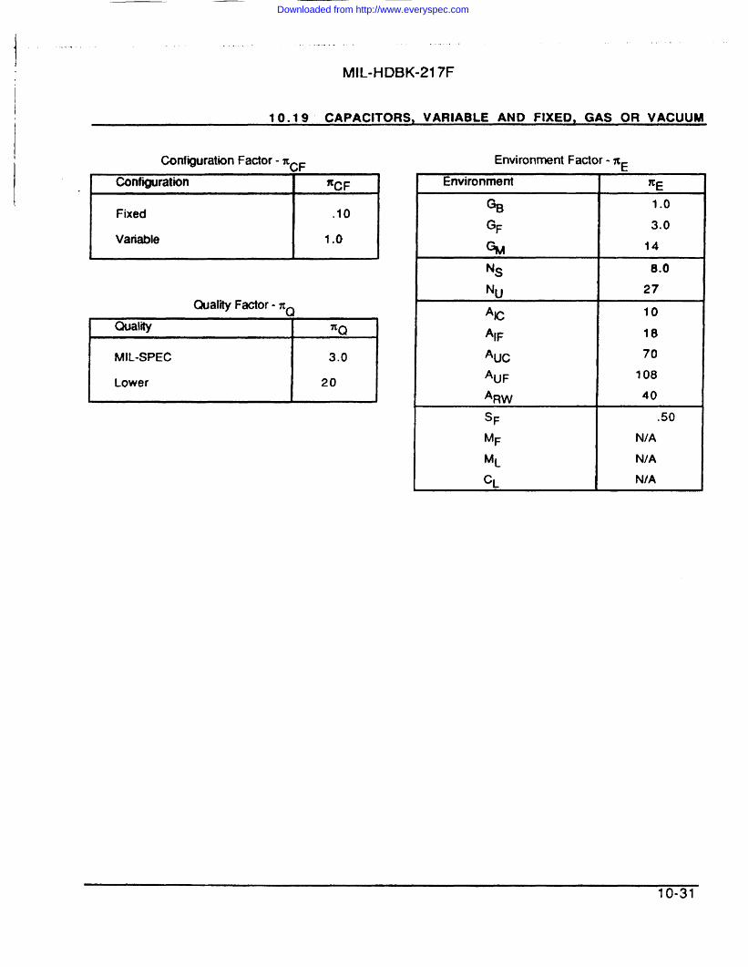
.,.I . !I ,.. ... .,, . . . . .
MIL-HDBK-217FI
10.19 CAPACITORS, VARIABLE AND FIXED, GAS OR VACUUM
ConfigurationFactor - TCCF--Conf~ratkm ‘C F
Fixed .10
Variable 1.0
QuaIii Factor- XQ
Quality ~ Q
MIL-SPEC 3.0
Lower 20
Environment Factor - fiE
Environment ~E
% 1.0
GF 3.0
GM 14
Ns 8.0Nu 27
AC 10
‘IF 18
*UC 70
*UF 108
‘RW 40
SF .50
MF NIA
ML NIA
cL NIA
Downloaded from http://www.everyspec.com
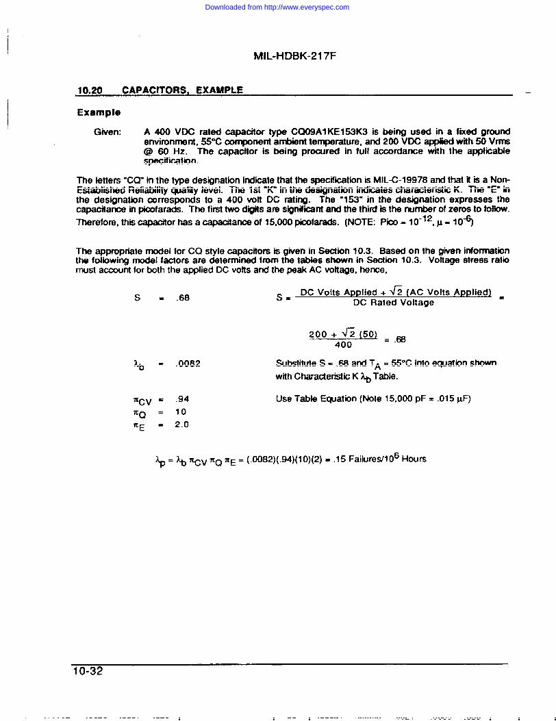
MIL-HDBK-217F
10.20 CAPACITORS, EXAMPLE —
Example
Given: A 400 VDC rated capacitor type CQ09A1 KE153K3 is being used in a fixed groundenvironment, 59C component ambient temperature, and 200 VDC applied with 50 Vrms@ W Hz. The Capadtor iS Ming procured in full accodance with the applicablespecification.
The letters “CQ- h the type designation hdkate that the specification is MIL-C-19978 and that it is a Non-Established Reliability qualii level. The Ist “K” in the designation indicates characteristic K. The “E” inthe designation corresponds to a 400 vott DC rating. The “153” in the designation expresses thecapacitance in pioofarads. The first two digits are signifiint and the third is the number of zeros to follow.Therefore, this capacitor has a capacdance of 15,000 picofarads. (NOTE: Picos 10-12, p = 10~
The appropriate model for CQ style capacitors is given in Section 10.3. Based on the given informationthe following model factors are determined from the tables shown in Section 10.3. Voltage stress ratiomust account for both the applied DC volts and the peak AC vottage, hence,
s = .68
lb = .0082
7ECV = .94
7C Q = 10
~E = 2.0
S = DC Volts Applied + ~2 (AC Volts Armlied~ =DC Rated Voltage
Substitute S = .68 and TA = 55°C into equatbn shown
withCharacteristicK ~ Table.
Use Table Equation (Note 15,000 pF = .015 pF)
~ = ~ ICcv nQ XE = (.0082)(.94)(1 O)(2) = .15 FailuresJl 06 Hours
10-32
Downloaded from http://www.everyspec.com

MIL-HDBK-217F
11.1 INDUCTIVE DEVICES, TRANSFORMERS
SPECIFICATION STYLE DESCRIPTIONMIL-T-27MIL-T-21038MIL-T-55831
TH~ (%)3035404550556065707580859095100105110115120125130135140145150155160165170175180185
NOTE: Themo
TF Audio, Power and High Power PulseTP Low Power Pulse
IF, RF and Discriminator
Xp = lb~QXE Failures/l 06 Hours,
Base Faiture Rate - ~Maxinwm Rated OperatingTemperature (“C)
~~1
.0024
.0026
.0028
.0032
.0038
.0047
.0060
.0083
.012
.020
.036
.075
-}1s are valtd onl
1052.0023.0023.0024.0025.0027.0029.0032.0035.0040.0047.0057.0071.0093.013.019.030
,~3
.0022
.0023
.0024
.0025
.0026
.0027
.0029
.0030
.0033
.0035
.0039
.0043
.0048
.0054
.0062
.0072
.0085
.010
.013
.016
.020
, =4
.0021
.0022
.0022
.0022
.0023
.0023
.0023
.0024
.0025
.0026
.0027
.0028
.0029
.0031
.0033
.0035
.0038
.0042
.0046
.0052
.0059
.0068
.0079
.0095
.011
.014
1705.0018.0018.0019.0019.0020.0020.0021.0021.0022.0023.0024.0024.0025.0026.0027.0028.0030.0031.0032.0034.0036.0038.0040.0042.0044.0047.0050.0053.0056
-if THS ISnot above the temperature rating for a given insulation class.
1 fiHS + 273\ lSs
>1706.0016.0016.0016.0016.0017.0017.0017.0017.0017.0017.0017.0017.0018.0018.0018.0018.0019.0019.0019.0020.0020.0021.0021.0022.0023.0024.0025.0026.0027.0029.0030.0032
“ \..oolat?xp ---=\ )
MIL-T-27 Insdatmn Class 0, MIL-T-21038 Insulation Class C?,and MlL-T-5563I tnsuhon Class O.”
MIL-T-27 Insulation Class R, MIL-T-21 038 Insulation Class R, and MIL-T-55831 Insulation Class A.”
3 +-’18’*F=)87MIL-T-27 Insulation Class S, MlL-T-2I 038 Insulation Class S, md MIL-T-S5631 Insulation Class B.”
4 +’=m2ex’c”:~273)i0MIL-T-27 Insulation Class V, MIL-T-21 038 Insulation Class T, and MIL-T-s5631 Insulation Class C,*
‘ ~-om’-’(”:”)””)”MIL-T-27 Insulation Class T and MIL-T-21 038 Insulation Class U.*
‘ ~-m’w”x’(TH:;:73)8”4MIL-T-27 Insulation Class U and MIL-T-21038 Insulanon Class V “
‘w . Hot Spot Temperature (%), See Se&h 11.3. “Rotor to Transformer Application Not- tor Oatormlnstlon of Irwulatlon ClassI
11-1
Downloaded from http://www.everyspec.com
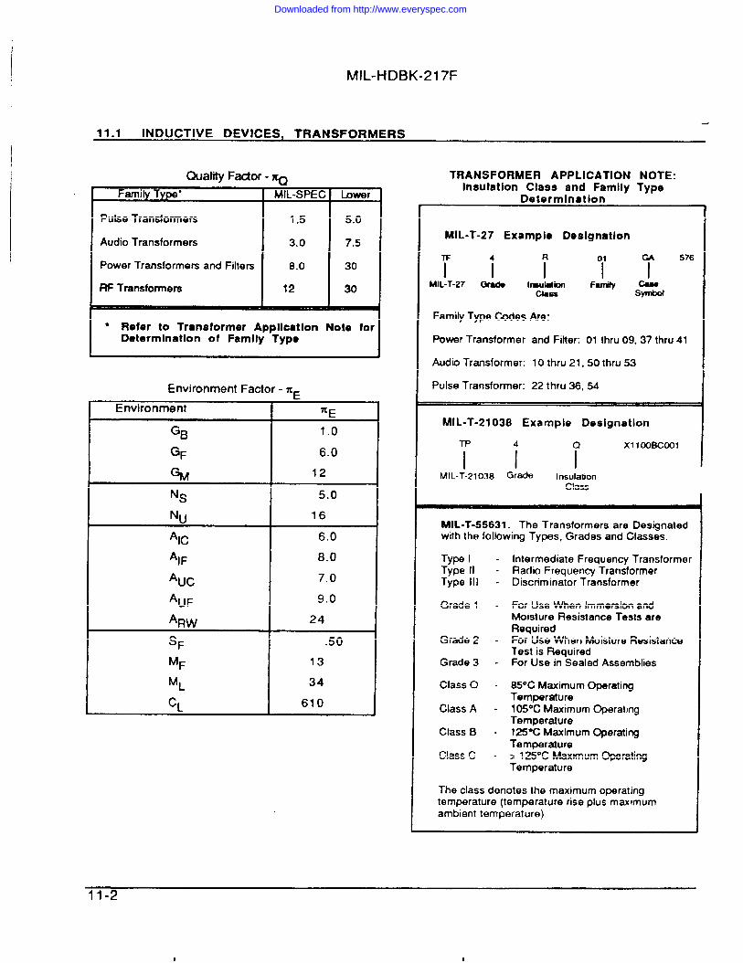
MIL-HDBK-217F
11.1 INDUCTIVE DEVICES, TRANSFORMERS
Quality Factor - ~Family Type” 1 MIL-SPEC I Lower
IPulse Transformers
Audio Transformers
Power Transformers and Filters
RF Transformers
1.5I
5.0
3.0 7.5
8.0 30
12I
30
● Refer to Transformer Appllcatlon Note forDetermlnatlon of Family Typ.
Environment Factor - ZE
Environment ~E
GB 1.0
GF 6.0
% 12
Ns
Nu
Alc‘IF
*UC‘UF
‘RWSF
MF
5.0
16
6.0
8.0
7.0
9.0
24
.50
13
34
610
TRANSFORMER APPLICATION NOTE:Insulation Class and Family Type
Determination
MIL-T-27 Example Deslgnatlon
TF 4
I I
R
I01 m 576
I IMIL-T-27 Grad, Imldabrl Fatity ~
Clasa symbol
Family Type Codes Are:
Power Transformer and Filter: 01 thru 09, 37 thru 41
Audio Transformer: 10 thru 21, 50 thru 53
Pulse Transformer: 22 thru 36, 54
MI L-T-21038 Example Designation
TP 4 Q X11 OO8COO1
I I IMIL-T-21038 Grade Insulation
Class
MIL-T-55631. The Transformers are Designatedwith the following Types, Grades and Classes.
Type IType IIType Ill
Grade 1
Grade 2
Grade 3
Class O
Class A
Class B
Class C
.
.
.
.
-
Intermediate Frequency TransformerRadio Frequency TransformerDiscriminator Transformer
For Use When immersion andMoisture Resistance Tests areRequiredFor Use When Moisture ResistanceTest is RequiredFor Use in Sealed Assemblies
85oC Maximum OperatingTemperature105°C Maximum OperaiingTemperature12SeC Maximum OperatingTemperature> 125°C Maximum OperatingTemperature
The class denotes the maximum operatingtemperature (temperature rise plus maximumambient temperature).
11-2
Downloaded from http://www.everyspec.com
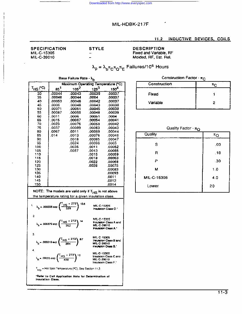
MIL-HDBK-217F
11.2 INDUCTIVE DEVICES, COILS
SPECIFICATION STYLEMIL-C-15305MIL-C-3901O
Xp = kbnc7cQ7LE
TH~ (oC)
3035404550
E65707580859095100105110115120125130135140145150
Base Failure Rate - ~Maximum Operating Temperature ~C)
851 1052 1253 1504.00044 .00043 .00039 .00037.00048.00053.0006.00071.00087.0011.0015.0023.0037.0067.014
.00044
.00046
.00048
.00051
.00055
.0006
.00067
.00076
.00089
.0011
.0013
.0018
.0024
.0036
.0057
.0004
.00042
.00043
.00045
.00048
.00051
.00054
.00058
.00063
.00069
.00076
.00085
.00096
.0011
.0013
.0015
.0018
.0022
.0028
.00037
.00037
.00038
.00038
.00039
.0004
.00041
.00042
.00043
.00044
.00046
.00047
.0005
.00052
.00055
.00059
.00063
.00068
.00075
.00083
.00093
.0011
.00120014
NOTE: The models are valid onty if THS is not abovethe ternperature rating for a given insulation class.
“ ~=mmex’(’”:~:’’)””’,n$u~onc,-$oMlL-C- 15305
2MlL-C-l 5305
‘=m’gexp(’”:;:’”)” ,~u~~c,wA,InsulationClassA andMIL.C-3901 o
3.
~--19exp(TH::27a)e”74.
MIL-C-15305InsulationClass B andMIL-C-3901OInsulationChseeB.”
MIL-C-I 5305InsulationClassC andMIL-C-3901OInsulationClass F .“
‘HS = HotSpotTemperature(“C), See Sectionf 1.3.
“Refer to Coil Appllcetlon Note for Determhmtlon ofInaulatlon Claes.
DESCRIPTIONFixed and Variable, RFMoided, RF, Est. Rel.
Failures/l 06 Hours
Construction Factor - XcConstruction Zc
Fixed
I1
Variable 2
Quality Factor - ~Quality 7rQ
s .03
R .10
P .30
M 1.0
MIL-C-15305 4.0
Lower 20
11-3
Downloaded from http://www.everyspec.com
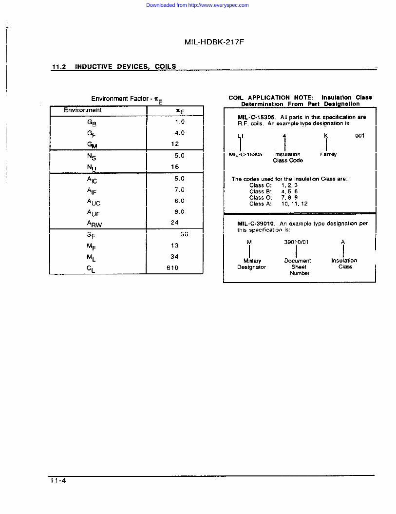
MIL-HDBK-217F
11.2 INDUCTIVE DEVICES, COILS —
Environment Factor - ZE
Environment ~E
GB 1.0
GF 4.0
% 12
Ns 5.0
Nu 16
Ac 5.0
‘IF 7.0
*UC 6.0
*UF 8.0
‘RW 24
SF .50
MF 13
ML 34
CL 610
COIL APPLICATION NOTE: Infsulatlon ClassDetermination From Part Designation
MlL-C-l 5305. All parts in this specification areR.F. wils. An example type designation is:
LT
I
4
IMIL--G153O5 Insulation Famify
Class Code
The codes used for the Insulation C&ss are:Class C: 1,2,3Class B: 4, 5, 6Class O: 7, 8, 9Class A: 10,11,12
001
MI L-C-3901 O. An example type designation perthis specification is:
M
I
39010/01 A
I IMilitary Document Insulation
Designator Sheet classNumber
11-4
Downloaded from http://www.everyspec.com
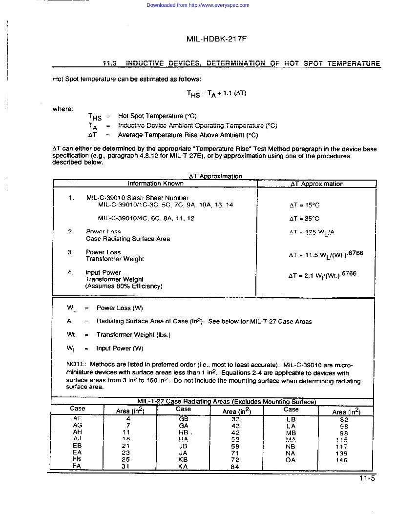
MIL-HDBK-217F
11.3 INDUCTIVE DEVICES, DETERMINATION OF HOT SPOT TEMPERATURE
, Hot Spot temperature can be estimated as follows:
THS=TA+ 1.1 (AT)
where:THS = Hot Spot Temperature (“C)TA = Inductive Device Ambient Operating Temperature (“C)AT = Average Temperature Rise Above Ambient (“C)
AT can either be determined by the appropriate “Temperature Rise- Test Method paragraph in the device basespecification (e.g., paragraph 4.8.12 for M IL-T-27 E), or by approximation using one of the proceduresdescribed below.
.
AT ApproximationInfnrmatinn Knnwn 1 AT Annrqximation.. ... .. ... . .“. , ,., ,”.... -, .yp. w —. —
1. MIL-C-3901 O Slash Sheet NumberMIL-C-39010/l C-3C, 5C, 7C, 9A, 10A, 13, 14 AT = 15°C
tvllL-c-39010/4C, 6C, 8A, 11, 12 AT = 35°C
2. Power Loss AT= 125 w@Case Radiating Surface Area
3. Power LossTransformer Weight AT= 11.5 WL/(Wt.).6766
4. Input Power AT = 2.1 w,/(w@66Transformer Weight(Assumes 80% Efficiency)
w~ = Power Loss (W)
A = Radiating Surface Area of Case (in2). See below for MIL-T-27 Case Areas
wt. = Transformer Weight (Ibs.)
w, = Input Power (W)
NOTE: Methods are listed in preferred order (i.e., most to least accurate). MIL-C-3901 Oare micro-miniature devices with surface areas less than 1 in2. Equations 2-4 are applicable to devices withsurface areas from 3 in2 to 150 in2. Do not include the mounting surface when determining radiatingsurface area,
MIL-T-27 Case Radiating Areas (Excludes Mounting Surface)Case Area (in*) Case Area {in2) Case Area (in2)AF 4 GB 33 LB 82AG 7 GA 43 LA 98AH 11 HB . 42 MB 98AJ 18 HA 53 MA 115EB JB 58 NB 117EA ;; JA 71 139FB 25 KB 72 :: 146FA 31 KA 84
11-5’
Downloaded from http://www.everyspec.com
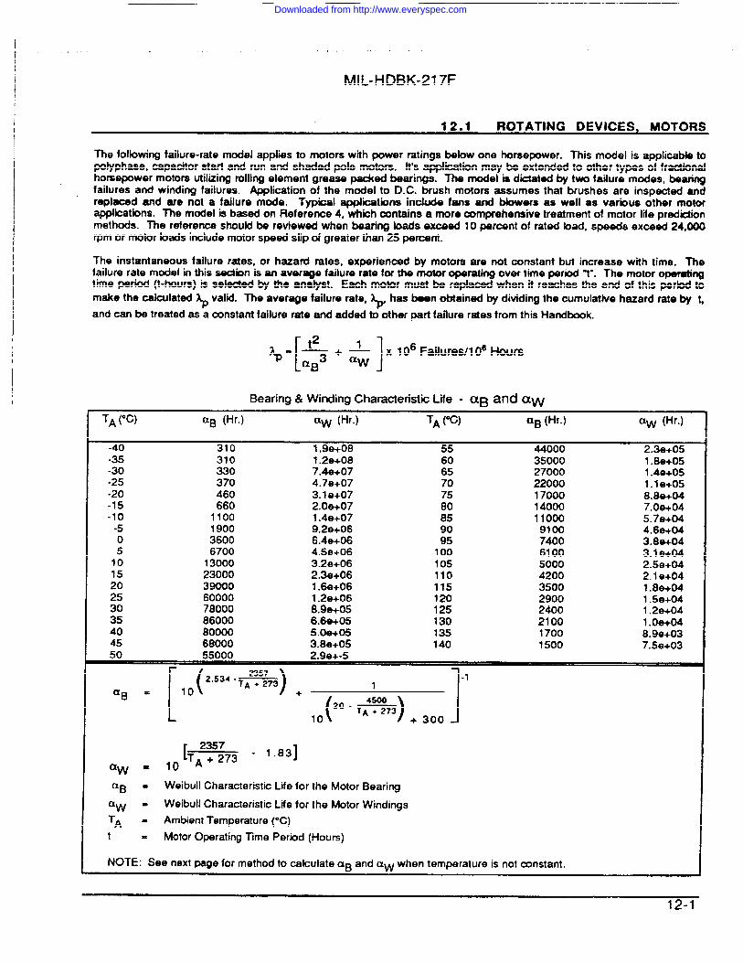
I1
MIL-HDBK-217F
I 12.1 ROTATING DEVICES, MOTORSII
The following failure-rate model appiies to motors with power ratings betow one horsepower. This model is applicable topolyphase, capacitor start and run and shaded pole motors. It’s application may be extended to other types of fractionalhorsepower motors utilizing rolling element grease packed bearings. The rndel is dictated by two failure modes, bearingfailures and winding failures. Application of the model to D.C. brush motors assumes that brushes are inspected andreplaced and are not a failure mode. Typical appkations include fans and Mowers as well as various other motorapplications. The model is based on Referenoe 4, which oontains a more comprehensive treatment of motor life precktionmethods. The reference should be reviewed when bearing loads exceed 10 percent of rated bad, speeds exceed 24,000rpm or motor back include motor speed slip of greater than 25 percent.
The instantaneous failure rates, or hazard rates, experienced by motors are not oonstant but increase with time. Thefailure rate model in this sectbn is an average failure rate for the motor operating over time period “t”. The motor operatingtime period (t-hours) is selected by the analyst. Each motor must be replaced when it reaches the end of this perbd tomake the calculated ~ valid. The averaga failure rate, ~, has been obtained by dividing the cumulative hazard rate by t,and can be treated as a constant failure rate and added to other part failure rates from this Handbook.
I
%[~2 1=—3+~
1x 10⁶ Failures/l 06 H0ur6
UB
Bearing & Winding Characteristic Life - aB and aw
TA ~C) aB (Hr.) aw (Hr.) TA (oC) aB (Hr.) aw (Hr.)
-40 310 1.9e+08 55 44000 2.3e+05-35 310 1.2e+08 60 35000 1.8e+05-30 330 7.4e+07 65 27000 1.4e+05-25 370 4.78+07 70 22000 1.1 e+05-20 460 3.1 e+07 75 17000-15
8.8e+04660 2.0e+07 80 14000 7.0e+04
-lo 1100 1.4e+07 85 11000 5.7e+04-5 1900 9.2e+06 9100 4.6e+04o 3600 6.4e+06 E 7400 3.8e+045 6700 4.5e+06 100 610010
3.le+0413000 3.2e+06 105 5000 2.5e+04
15 23000 2,3e+06 110 4200 2.1 e+0420 39000 1.6e+06 115 3500 1.8e+0425 60000 1.2e+06 120 290030 78000
1.5e+048.9e+05 125 2400 1.2e+04
35 86000 6.60+05 130 2100 1.oe+0440 80000 5.oe+05 135 1700 8. 9e+0345 68000 3.8e+05 140 1500 7.5e+0350 55000 2.9e+-5
[
(
23572’534 ‘7A + 273
)
1- 1
10 1aB = +
(20- 4500
7A + 27310 ) + 300
[2357
TA + 273 - 1 .83]aw = 10aB = Weibull Characteristic Life for the Motor Bearing
aw s Weibull Characteristic Life for the Motor WindingsTA - Ambient Temperature (“C)t = Motor Operating Time Period (Hours)
NOTE: See next page for method to calculate aB and aw when temperature is not constant.
12-1
Downloaded from http://www.everyspec.com
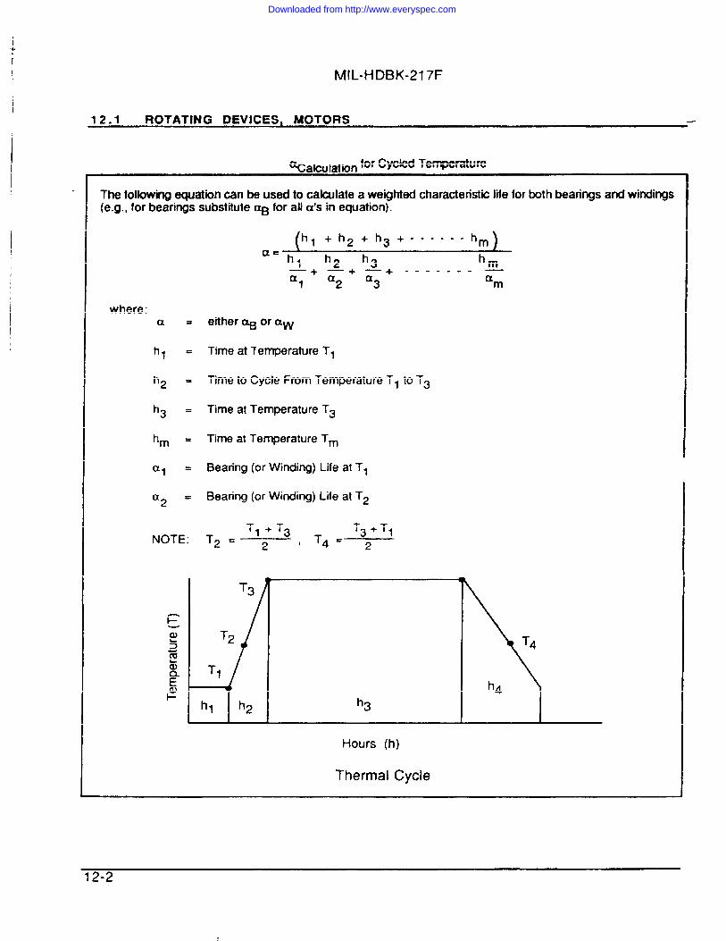
MIL-HDBK-217F
12.1 ROTATING DEVICES, MOTORS
%.ala Ilation ‘Or cYcled ‘eWr*ure
The following equation can be used to calculate a weghted characteristic life for both bearings and windings(e.g., for bearings substitute aB for all a’s in equation).
h1+h2+h3+------hm
hm—+ —+ — +-------—al a2 a3 am
where:a= either (%Bor aw
h, = Time at Temperature T,
h2 = Time to Cycle From Temperature T, to T3
h3 = Time at Temperature T3
hm = Time at Temperature Tm
al = Bearing (or Winding) Life at T,
‘2 = Bearing (or Winding) Life at T2
T, + T3 T3 + T,NOTE: T2=2, T4=2
i=
T3
T2
T1
hl h2 h3
Hours (h)
Thermal Cycle
12-2
Downloaded from http://www.everyspec.com
MIL-HDBK-217F
12.2 ROTATING DEVICES. SYNCHROS AND RESOLVERS
NOTE:
DESCRIPTIONRotating Synchros and Resolvers
Lp = XbKSZNXE Failures/l 06 Hours
Synchros and resolvers are predominately used in service requiring only slow and infrequent motion.M-echanical wearout problenis are infrequent so that the electrical failure mode dominates, and nomechanical mode failure rate is required in the model above.
Tr (“C)
3035404550556065707580
Base FaiUre Rate - ~
.0083
.0088
.0095
.010
.011
.013
.014
.016
.019
.022
.027
TF (%)
859095100105110115120125130135
.032
.041
.052
.069
.094
.13
.19
.29
.45
.741.3
% = .00535 exp(T~:~3 )85
TF = Frame Temperature (“C)
If Frame Temperature is Unknown AssumeTF .40 ‘C + Ambient Temperature
Size Factor - XS
%sDEVICE Size 8 or Size 10-16 Size 18 orTYPE Smalier Larger
SynchroI
2 1.5 1
ResolverI
3 2.25 1.5
Number Of Brushes Factor - ~NNumber of Brushes %N
2
3
4
1.4
2.5
3.2
Environment Factor - YIC=
Environment
GB
GF
GM
NS
Nu
Aic
‘IF
*UC
‘UF
*RWSF
MF
ML
CL
L
~E
1.0
2.0
12
7.0
18
4.0
6.0
16
25
26
.50
14
36
680
12-3
—
Downloaded from http://www.everyspec.com
MIL-HDBK-217F
12.3 ROTATING DEVICES, ELAPSED TIME METERS —
DESCRIPTIONElapsed Time Meters
kp = kbycE Failures/l 06 Hours
Base Failure Rate - ~w
Type k~
A.C. 20
Inverter Driven 30
Commutator D.C. 80
Temperature Stress Factor - ZTOperating T (°C)/Rated T (“C) XT
o to .5 .5
.6 .6
.8 .8
1.0 1.0
Environment Factor - Xrb
Environment ZE
% 1.0
GF 2.0
GM 12
N~ 7.0
Nu 18
*IC 5.0
‘IF 8.0
*UC 16
‘UF 25
*RW 26
SF .50
MF 14
ML 38
CL NIA
12-4
Downloaded from http://www.everyspec.com
MIL-HDBK-217F
12.4 ROTATING DEVICES, EXAMPLE
Example
Given: Fractional Horsepower Motor operating at a thermal duty cycle of: 2 hours at 10O°C, 8hours at 20”C, 0.5 hours from 100°C to 20”C, and 0.5 hours from 20°C back to 100”C.Find the average failure rate for 4000 hours operating time.
The basic procedure is to first determine operating temperature at each time intewai (or avergetemperature when traversing from ow temperature to another, e.g. T2 = (100 + 20/2 = ~“c. ~te~inaB and aw at each temperature ati then use these vakes to determine a wei@kf average ~ and awto use in the ~ e~ation.
h, = 2 hr.
h2 = h4 = 0.5 hr.
h3 = 8 hr.
aB
aw
T, = 1OO”C; aB = 6100 hours; aw = 31000 hours
T2 = 60%; aB = 35000 hOUfS; aw = 180000 hOUR
T3 = 20”C; aB = 39000 hours; aw = 1600000 hours
2 +0.5+8+0.5=2 0.5 8 0.5 = 19600 hours
6100 + 35000 + 39000 + 35000
2 +0.5+8+0.5=2 0.5 8 0.5 = 146000 hOUB
31000 + 180000 + 1600000 + 180000
= (3++”0’(= (4000)2 1
+ 146000)X106
(19600)3
= 9.0 FaihxeW 06 Hours
12-5
Downloaded from http://www.everyspec.com
MIL-HDBK-217F
13.1 RELAYS, MECHANICAL
SPECIFICATION DESCRIPTIONMIL-R-5757 MIL-R-19648 Mechanical RelayMIL-R-6106 MIL-R-83725MI L-R-19523 MIL-R-83726 (Except Class C, Solid State Type)MIL-R-39016
Lp = &XLZCZCYCXFXQXE Failures/l 06 Hours
TA (’W)
30354045505560
%7580859095100105110115120125
Base Failure Rate - ~Rated
85%+.0060.0061.0063.0065.0068.0072.0077.0084.0094.011.013.016.020
u—Temperature
125”c~.0059.0060.0061.0062.0064.0066.0068.0071.0074.0079.0083.0089.0097.011.012.013.015.018.021.025.031
1“%= 00’5’ex’cA::73)’5”72%= 00Mex’cAJ~73)’04TA . Ambient Temperature (oC)
Contact Form Factor - ~(Applies to Active Conducti ng Contacts)r
I Contact Form I ~c
DPSTSPDT3PST4PSTDPDT‘PDT4PDT
I 6PDT
1.501.752.002,503.004.255.508.00
Load Stress Factor - XLLoad Typo -I
s Resistive’ lnductive2 Lamp3.05 1.00 1.02.10 1.02 1.06 ; :Z.20 1.08 1.28 2.72.30 1.15 1.?6 9.49.40 1.28 2.72 54.6.50 1.48 4.77.60 1.76 9.49.70 2.15 21.4.80 2.72.90 3.551.00 —
1.()
~2 3.()
S2XL = @Xp ,8 XL = exp ~
2.()
s2~=~L = e’p ~ Operatino Load Current
Rated Resistive Load Current
For single devices which switch two different load types,evaluate XL for each possible stress load type
combination and use the worse case (largest ZL).
Cycling Factor - ~YCCycle Rate
(Cycles per Hour) ‘CYC(MI L-SPEC)
i-io~21.0 10<1.0 0.1
Cycle Rate(Cycles per Hour) WC
(Lower Quality)
(Cycles per Hour 2
>1000 100 )
I Cycles per Hour10-1000 10
NO~ :Values of ZCYC for cycling rates beyond the
basic design limitations of the relay are not valid.Design specifications should be consulted prior to
‘Va’uation‘f ‘CYC. I13-1
Downloaded from http://www.everyspec.com
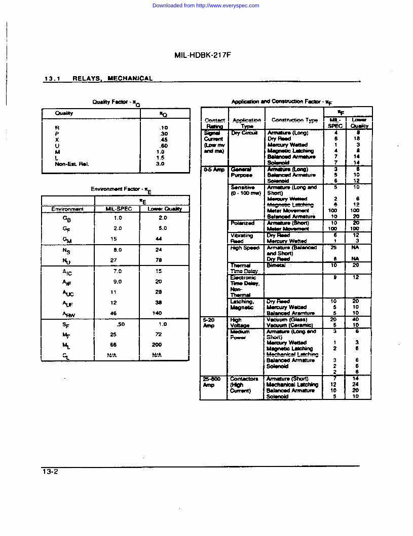
III
h41L-HDBK-217FI
13.1 RELAYS, MECHANICAL
Oualhy % 1R .10P
I.30
x .45 Iu .60ML :::Non-Est.Rol. 3.0
Envimnmont Factor -~
$tE,
Environment MIL-SPEC LowOrOudityGB 1.0
% 2.0
GM 15
NS 8.0
N 27i
*IC I 7.0
A~ 9.0
Auc 11
%F 12
46
SFI
.50
% 25
% I 66
cl WA
2.0
5.0
u
24
78
15
20
20
36
1’40
1.0
72
WA
I i II
con- ~tion ConstructionTypeb
Dry Rwd 6 18Ifbwmv[ I MofcuwWottod 11131.d In@ I
6 12ArmuW(lmngand 5 10
B8mcul Ammtuf6110 20Poi8fizod AwnmJro(short) 10 20
100 100I
MwcuryWettedHqh Spood ArrnmW@(081anc0d A 2
6 M
Elut mfiic 9 12
L&wTiu90Dd8y, I 1 -1-1Mching,MqymtiZ Uucury Wmttod 5 10
B8bcod Arwnturo 5 105-20 vaCwm (Gk!m) 20 40w Vaafwl (CkmmiC) 5 10
IPm-MdiurnIAnshort] ‘ - 11 I
2 6CWMctom (short) 7
w m Wchankd Latching 12 zCwu?t) OatuK#d Ann8tufo 10 20I 1~
. I 5 1 10 I
Iw 1 I I ,. =1 I -. I
Downloaded from http://www.everyspec.com
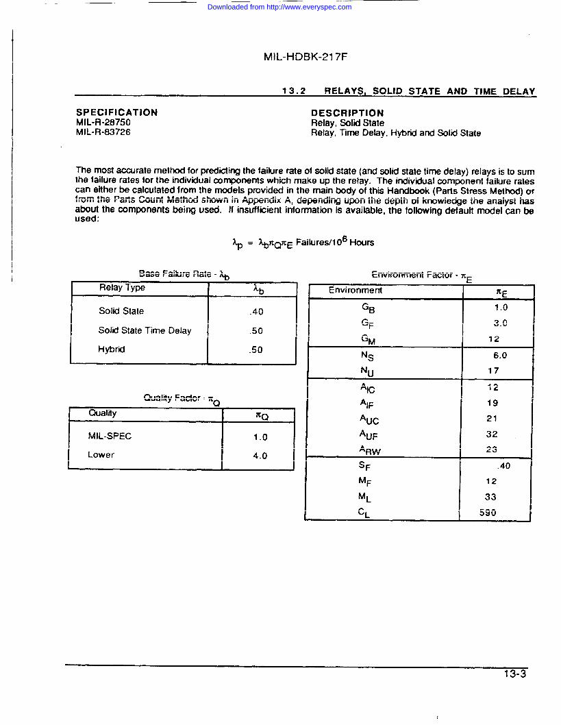
MIL-HDBK-217F
13.2 RELAYS, SOLID STATE AND TIME DELAY
SPECIFICATION DESCRIPTIONMIL-R-28750 Relay, Solid StateMIL-R-83726 Relay, Time Delay, Hybrid and Solid State
The most accurate method for predicting the failure rate of solid state (and solid state time delay) relays is to sumthe failure rates for the individual components which make up the relay. The individual component failure ratescan either be calculated from the models provided in the main body of this Handbook (Parts Stress Method) orfrom the Parts Count Method shown in Appendix A, depending upon the depth of knowledge the analyst hasabout the components being used. If insufficient information is available, the following cfefautt model can beused:
~ = ~X@E Failure@106 Hours
Base Faiiure Rate - ~Relay Type
Solid State
Solid State Time Delay
Hybrid
.40
.50
.50
Quality Factor - ZQ
Quality ~Q
IMIL-SPEC
I 1.0
Lower 4.0
Environment Factor - Xr
Environment nE
GB 1.0
GF 3.0
GM 12
NS 6.0
Nu 17
*tc 12
‘IF 19
‘Uc 21
*UF 32
‘RW 23
SF .40
MF 12
ML 33
CL 590
13-3
Downloaded from http://www.everyspec.com
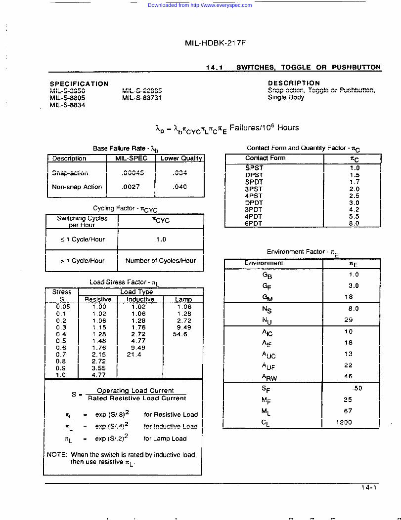
,+
MIL-HDBK-217F
14.1 SWITCHES, TOGGLE OR PUSHBUTTON
SPECIFICATION DESCRIPTIONMIL-S-3950 MIL-S-22885 Snap-action, Toggle or Pushbutton,MIL-S-8805 MIL-S-83731 Single BodyMIL-S-8834
Xp = kb7tcyc7cL7rc7zEFailures/l 06 Hours
Base Failure Rate - ~Description I MIL-SPEC 1 Lower Quality
Snap-action I .00045 I .034
Non-snap Action I .0027 I .040
Cycling Factor - Zcycb
Switching Cycles *CYCper Hour
s I Cycle/Hour 1.0
>1 Cycle/Hour Number of Cycles/Hour
Load Stress Factor - ~LStress Load Type -s Resistive Induct ive Lamp0.05 1.00 1.02 1.060.1 1.02 1.06 1,280.2 1.06 1.28 2.720.3 1.15 1.76 9.490.4 1.28 2.72 54.60.5 1.48 4.770.6 1.76 9.490.7 2.15 21.40.8 2.720.9 3.551.0 4,77
s= Operating Load CurrentRated Resistive Load Current
XL = exp (S/.8)2 for Resistive Load
XL = exp (S/.4)2 for Inductive Load
~L = exp (S/.2)2 for Lamp Load
NOTE: When the switch is rated by inductive load,then use resistive XL.
Contact Form and Quantity Factor - xcContact Form xc
SPST 1.0DPST 1.5SPDT 1.73PST 2.04PST 2.5DPDT 3.03PDT 4.24PDT 5.56PDT 8.0
Environment Factor - nE
Environment ~E
GB 1.0
GF 3.0
GM 18
Ns 8.0
NU 29
Alc 10
‘IF 18
‘Uc 13
*UF 22
‘RW 46
SF .50
MF 25
ML 67
CL 1200
14-1
I 1,., *mm.. I, ,- I .AA1.4WI .4 WI.*- fi .4Knw I
Downloaded from http://www.everyspec.com
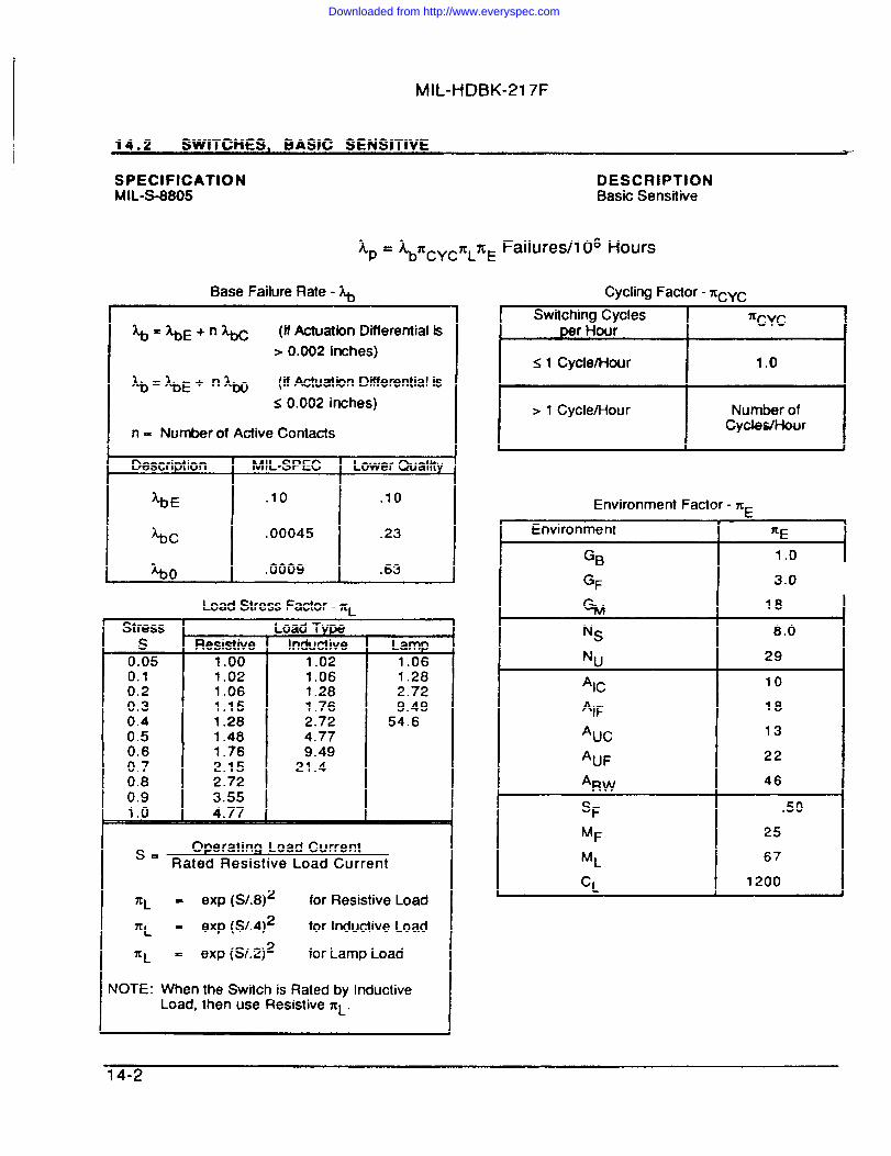
MIL-HDBK-217F
14.2 SWITCHES, BASIC SENSITIVE T
SPECIFICATION DESCRIPTIONMIL-S-88f)5 Basic Sensitive
Ap =L7C~ ~YCXLZE Failures/l 06 Hours
Base Failure Rate - ~ Cycling Factor - ncyc
%=%’JE’%C (if Actuation Differential is>0.002 inches)
~ = ~E + n ~ (if Actuation Differential is<0.002 inches)
n = Number of Active Contacts
Description MIL-SPEC Lower Quality
%E .10 .10
%C .00045 .23
‘bO .0009 .63
Load StreSs Factor -XLStress Load Types Resistive Inductive Lamp
0.05 1.00 1.02 1.060.1 1.02 1.06 1.280.2 1.06 1.28 2.720.3 1.15 7.76 9.49
1.28 2.72 54.6::: 1.48 4.770.6 1.76 9.490.7 2.15 21.40.8 2.720.9 3.551.0 4.77
s= Operatin~ Load CurrentRated Resistive Load Current
nL = exp (S/.8)2 for Resistive Load
XL = exp (S/.4)2 for Inductive Load
~L = exp (S/.2)2 for Lamp Load
NOTE: When the Switch is Rated by InductiveLoad, then use Resistive XL.
Switching Cycles ‘CYCper Hour
I 51 Cycle/Hour I 1.0 I
I >1 Cycle/Hour I Number ofCycles/Hour
I
Environment Factor - xc
Environment
GB
GF
%Ns
N“
*IC
‘IF
‘Uc
‘UF
*RWSF
MF
ML
Ci
I 4-L
1.0 I3.0
18
8.0
29
10
18
13
22
46
.50
25
67
1200
Downloaded from http://www.everyspec.com
MIL-HDBK-217F
I
14.3 SWITCHES, ROTARY
SPECIFICATION DESCRIPTIONMIL-S-3786 Rotary, Ceramic or Glass Wafer, Silver Alloy Cotiacts
kp = lb7ccycKL7cE Failures/l 06 Hours
Base Failure Rate - ~
Base failure rate model (~:
%=%E’%F (for Cemrnc RF Wafers)
%=%E+”~G (for Rotary Switch MediumPower Wafers)
n = Nu~r of Active co~ta~s
Description MIL-SPEC Lower Quality
‘b E .0067 .10
‘bF .00003 .02
%G .00003 .06
Load stress Faotor - ~LStress Load Typems Resistive Inductive Lamp
0.05 1.00 1.02 1.060.1 1.02 1.06 1.280.2 1.06 1.28 2.720.3 1.15 1.76 9.490.4 1.28 2.72 54.60.5 1.48 4.770.6 1.76 9.490.7 2.15 21.40.8 2.720.9 3.551.0 4.77
s. Operating Load CurrentRated Resistive Load Current
XL = exp (S/.8)2 for Resistive Load
XL = exp (S/.4)2 for Inductive Load
~L = exp (S/.2)2 for Lamp Load
NOTE: When the Switch is Rated by Inductive Load,then use Resistive XL.
Cycling Factor - ~ycb
Switching Cycles ‘CYCper Hour
I s 1 Cycle/HourI
1.0
I > 1 Cycle/Hour I Number of Cycles/Hour
Environment Factor - n-v Environment
GB
GF
GM
N~
Nu
Alc
‘IF
%
‘UF
‘RW1SF
MF
ML
CL,
1.0
3.0
18
8.0
29
10
18
13 -
22
46
.50
25
67
1200
Downloaded from http://www.everyspec.com
MIL-HDBK-217F
,.
14.4 SWITCHES, THUMBWHEEL —
SPECIFICATION DESCRIPTIONMIL-S-2271O Switches, Rotary (Printed Circuit) (Thumbwheel, ln-Line and Pushbutton)
Zp = (~1 + XN %2) XCYCZLXE Failures/l 06 Hours
CAUTION: This model applies to the switching function only. The model does not consider the contribution of anydiscrete components (e.g., resistors, diodes, lamp) which may be mounted on the switch. If significant(relative to the switch failure rate), the failure rate of these devices must be calculated using theappropriate sectionof this Handbook and added to the failure rate of the switch.
This model applies to a single switch seotion. This type of switch is frequently ganged to provide therequired function. The model must be applied to each section individually.
Base Failure Rate - kbl and %2
I %1
——
1 Description MIL-SPEC Lower Quality
.0067 .086
I ‘b 2 .062 .089
Number of Active Contacts Factor - ZN
I ~N = Number of Active ContactsI
Load Stress Factor - ZIStress Load Types Resistive inductive Lamp
0.05 1.00 1.02 1.060.1 1.02 1.06 1.280.2 1.06 1.28 2.720.3 1.15 1.76 9.490.4 1.28 2.72 54.60.5 1.48 4.770.6 1.76 9.490.7 2.15 21.40.8 2.720.9 3.551.0 4.77
s= Operating Load CurrentRated Resistive Load Current
XL = exp (S/.8)2 for Resistive Load
XL = exp (S/.4)2 for Inductive Load
2 for Lamp LoadXL = exp (S/.2)
NOTE: When the Switch is Rated by InductiveLoad, then use Resistive XL.
Cycfing Factor- XCYCSwitching Cycles
I ‘CYCDer Hour
I s 1 Cycle/Hour 1.0
I > 1 Cycie/Hour I Number of Cycles/Hour I
Environment Factor - x=
Environment
GB
GF
N~
Nu
Aic
‘IF
‘Uc
‘U F
‘RWSF
MF
ML
CL
~E
1.0
3.0
18
8.0
29
1018
13
22
46
.50
25
67
1200
14-4
Downloaded from http://www.everyspec.com
I MIL-HDBK-217F
14.5 SWITCHES, CIRCUIT BREAKERS
SPECIFICATIONM IL-C-55629MIL-C-83363MIL-C-39019w-c-375
I
DESCRIPTIONCircuit Breakers, Magnetic, Unsealed, Trip-FreeCircuit Breakers, Remote Control, Thermal, Trip-FreeCircuit Breakers, Magnetic, Low Power, Sealed, TripFree ServiceCircuit Breakers, MoJded Case, Branch Circuit and Service
= &cnUZQKE Failures/l 06 Hours
Base Failure Rate - ~Description
1Lb
1 I MagneticI
.020 I/ I Thermal
I.038
II
IThermal-Magnetic
I.038 I
Configuration Factor - XC
Configuration Zc
SPSTDPST3PST4PST
1.02.03.04.0
Use Factor - m tu
Use lru
Not Used as a PowerOtiOff Switch
1.0
Also Used as a Power 10On/Off Switch
Quality Factor - XQQuality * Q
Ii
MIL-SPEC 1.0
Lower 8.4*
Environment Factor - n=
Environment
GB
GF
GM
Ns
Nu
An
‘IF
*UC
*UF
*RWSF
MF
ML
CL
1.0
2.0
15
8.0
27
7.0
9.0
11
12
46
.50
d
25
66
tWA
14-5
n7c I I 1 . ---- . ..A Ann
Downloaded from http://www.everyspec.com
MIL-HDBK-217F
II 15.1I CONNECTORS, GENERAL (EXCEPT PRINTED CIRCUIT BOARD)I
I SPECIFICATION” DESCRIPTIONMM
.MMMMMMM
I●1
IL-C-24308 Rack and PanelIL-C-28748IL-C-28804IL-C-83513
L-C-5015 CimdarIL-C-264821~L-C-38999L-C-81 511
JOTE: See following page for connector configurations.
sMMMMMMMMMM
EDIFICATION* DESCRIPTION.“C-3607 Coaxial, RF.-c-3643.-C-3650.-c-3655.-C-25516.-(2-3901 2.-C-55235.-c-55339.-C-3767.-C-22992
MIL-C-49142
Power
Triaxial, RF
Ap = AbZ~ZpnE Failures/l 06 Hours
APPLICATION NOTE: The failure rate model is for a mated pair of connectors. It is sometimes desirable to assgnhalf of the overall mated pair connector (i.e., single connector) failure rate to the line replaceable unit and half to thechassis (or backplane). An example of when this would be beneficial is for input to maintainability prediction to allow afailure rate weighted repair time to be estimated for both the LRU and chassis. This accounting procedure could besignificant if repair times for the two halves of the connector are substantially different. For a single connector divide kp bytwo.
To (oC)
;:30405060708090
100110120130140150160170180190200210220230240250r -
Base Faiture Rate - ~Insert Material*
Al f32 & D4
.00006 .00025 .0021 .0038
.00008
.00009
.00011
.00014
.00016
.00020
.00023
.00027
.00032
.00037
.00043
.00050
.00059
.00069
.00080
.00094
.0011
.0013
.0016
.0019
.0023
.0028
.0034
.0042
.00033
.00044
.00057
.00073
.00093
.0012
.0015
.0019
.0023
.0029
.0036
.0045
.0056
.0070
.0087
.011
.014
.018
.022
.029
.0026
.0032
.0040
.0048,0059.0071.0087.011.013.016.020.024
.0048
.0062
.0078
.0099
.013,016.020.026.033.043.056.074
.0053
“ ff a mating pair of connectors uses two types ofinsert materials, use the average of the base failurerates for the two insert material types. See followingpage for inserl material determination.
Base Failure Rate - ~ (oont’d)
((0+=’)+ ~0x73)53’;‘ . ~= .020 ~xp ~-lsgz.o
((.+’7’)+(R:’y”)2. ~= .431 exp T-’073.6
((0+4+(%:7’)42’)3. ~= .190e~p T-1298.0
((0+27’)+ ~0&:73)4”72)4. ~ = .770 exp ~-1528.8
To = Internal Contact Operating Temperature (“C)
To = Connector Ambient Temperature + InsertTemperature Rise
See folbwing page for Insett Temperature RiseDetermination.
Downloaded from http://www.everyspec.com
I
I
MIL-HDBK-217F
15.1 CONNECTORS, GENERAL (EXCEPT PRINTED CIRCUIT BOARD)
Insert Material Determination— —‘-Possible Insert
MaterialsConf guration Specification A B ‘c DRack and Panel MIL-C-28748 x
M IL-C-83733 xMIL-C-24308 x xM IL-C-28804 x xMIL-C-83513 x x
Circular MIL-C-5015 x xMIL-C-26482 x x xMIL-C-28840 x xMIL-C-38999 x xMIL-C-8151 1 xMI L-C-83723 x
Power MI L-C-3767 x xMIL-C-22992 x x
Coaxial MI L-C-3607 xMIL-C-3643 xMIL-C-3650 xMI L-C-3655 xMIL-C-25516 xMIL-C-39012 xMI L-C-55235MIL-C-55339 x :
Triiial MIL-C-49142 x xInsertMaterial TemperatureType Common Insert Materials Ran~e (“C)*A Vitreous Glass, Alumina -55 to 250
Ceramic, PolyimideB Diallylphtalate, Melamine, -55 to 200
Fluorosilicione, SiliconeRubber, Polysulfone,Epoxy Resin
c Polytetrafluorethy lene -55 to 125(Teflon),Chbrotrifluorethylene(Kel-f)
D Polyamide (Nylon), -55 to 125Polychloroprene
~ne
These temperature ranges indicate maximum=pability of the insert material only. ConnectorsJsing these materials generally have a reducedemperature range caused by other considerations of:onnector design. Applicable connectorspecifications contain connector operatingemperature range,
Insert Tempe rature Rise (AT “I
*3456789101520253035
813192736465770
40
ContacI2025813182330374596
w
) Determination
1612458101316194170106
12T
1
;34567152639547292
AT = 0.989 (i)l ’85 22 Gauge ContactsAT = 0.640 (i)’ “85 20 Gauge ContactsAT = 0.274 (i)’ ’85 16 Gauge ContactsAT = 0.100 (i)l “85 12 Gauge Contacts
AT = Insert Temperature Risei = Amperes per Contact
RF Coaxial Connectors AT= 5°C
RF Coaxial Connectors(High Power Applications) AT = 50”C
Mating/Unmating Factor - KKMating/Unmating Cycles*(per 1000 hours) nK
o to .05 1.0> .05 to .5 1.5>.5t05 2.0>5t050 3.0> 50 4.0
●One cycle includes both connect and disconnect.
Downloaded from http://www.everyspec.com
—
II
MIL-HDBK-217F
I
15.1 CONNECTORS, GENERAL (EXCEPT PRINTED CIRCUIT BOARD)II
Active Pins Factor - nNumber ofActive
Cent acts
;3456
:910111213141516171819202530354045505560
Xp
1.01.41.61.7
;::
:::2.42.62.72.93.03.13.33.43.63.73.94.04.85.66.57.48.49.51112.
Number ofActive
Contacts
65707580859095100105110115120125130135140145150155160165170175180185190195200
13151618
E232527303235374043465053576165697478838994100
q = 0.51064
N = Number of Active Contacts
An active contact is the conductive element in aoonnector which mates with another element forthe purpose of transferring electrical energy. Forooaxial and triaxial oonneotors, the shieldcontact k oounted as an active contact.
Environment Factor - XE
~E
Environment MIL-SPEC Lower QualityGB 1.0 2.0
GF 1.0 5.0.
% 8.0 21
Ns 5.0 10
Nu 13 27
*IC 3.0 12
% 5.0 18
%c 8.0 17
‘UF 12 25
‘RW 19 37
SF .50 .80
MF 10 20
ML 27 54
CL 490 970
15-3
1 I
Downloaded from http://www.everyspec.com
MIL-HDBK-217F
15.2 CONNECTORS, PRINTED CIRCUIT BOARD
SPECIFICATIONMIL-C-21097MIL-C-55302
To (“C)
o102030405060708090100
Base Faiture Rate - L
.00012
.00017
.00022
.00028
.00037
.00047
.00059
.00075
.00093
.0012
.0015
To (<)
110120130140150160170180190200
Ab
.0018
.0022
.0028
.0035
.0044
.0055
.0069
.0088
.011
.015
To = Internal Contact Operating Temperature (°C)
DESCRIPTIONOne-Piece ConnectorTwo-Piece Connector
Failures/l 06 t-iours
Connector TerAmperesPer Contact
12345
mrature Ri:c
26
28162741
! (AT ‘C) Determinationtntad Guac
22
1481319
I
20
125813
AT = 2.100 (i)’.85 26 Guage ContactsAT = 0.989 (i)l .85 22 Guage ContactsAT = 0.640 (i)’-85 20 Guage Contacts
AT = Contact Temperature Rise
i = Amperes per Contact I
Mating/Unmating Factor - XKl’vlating/Unmating Cycles*(Perl 000 Hours)
o to .05> .05 to .5>.5t05>5t050
>50
1.01.52.03.04.0
● A cycle is defined as the mating and unrnatingof a connector.
15-4
I
Downloaded from http://www.everyspec.com
MIL-HDBK-217F
15.2 CONNECTORS, PRINTED CIRCUIT BOARD
Number ofActive
Contacts
12345678910111213141516171819202530354045505560
Active Pins Factor - z
*P
1.01.41.61.71.92.0
:::2.42.62.72.9
H3.33.43.63.7
:::4.85.66.57.4
!;1112
Number ofActive
Contacts
%7580
E
196105110115120125130135140145150155160165170175180185190195200
1315161819
:;2527303235374043465053576165697478
:;94
100
()N-1 qnp = exp ~
c1 = 0.51064
N = Number of Active Pins
An active contact is the conductive elementwhich mates with another element for thepurpose of transferring electrical energy.
Environment Factor - ~
~E
Environment MIL-SPEC Lower C?ualit~GB 1.0 2.0
GF 3.0 7.0
GM 8.0 17
Ns
Nu
Alc
*UC
*UF
‘RWSF
MF
ML
c,
5.0
13
6.0
11
6.0
11
19
.50
10
27
490
10
26
14
22
14
22
37
.80
20
54
970
15-5
Downloaded from http://www.everyspec.com
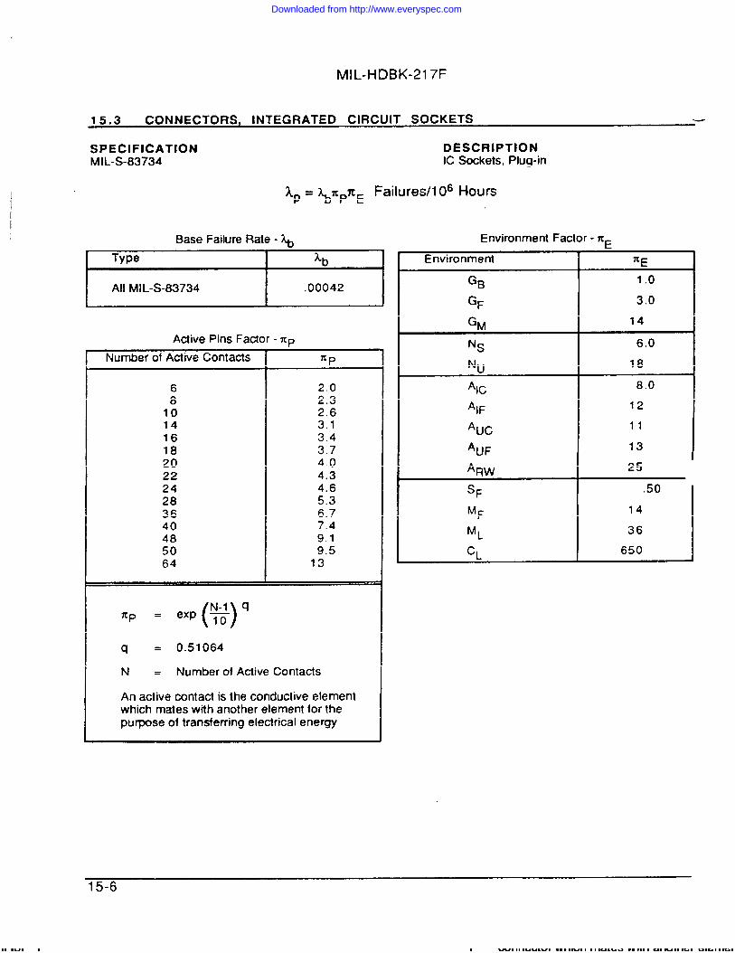
MIL-HDBK-217F
SPECIFICATION DESCRIPTIONMIL-S-83734 IC Sockets, Plug-in
‘P = %ZPXEFailuresll 06 Hours
Base Failure Rate - ~ Environment Factor - XEr
Type ?b~ Environment ~EI I
All MIL-S-83734 .00042 GB 1.0
GF 3.0
Active Pins Factor - npNumber of Active contacts 7tp
6 2.08 2.310 2.614 3.116 3.418 3.720 4.022 4.324 4.628 5.336 6.740 7.448 9.150 9.564 13
()
N-1 qnp = exp ~
q = 0.51064
N = Number of Active Contacts
An active contact is the conductive elementwhich mates with another element for thepurpose of transferring electrical energy.
GM
INS
Nu
Alc
‘IF
*UC
*UF
‘RWSE
MF
ML
I CL
14
6.0
18
8.0
12
11
13
25
.50
14
36
650
15-6
-. --- --- .- .
Downloaded from http://www.everyspec.com
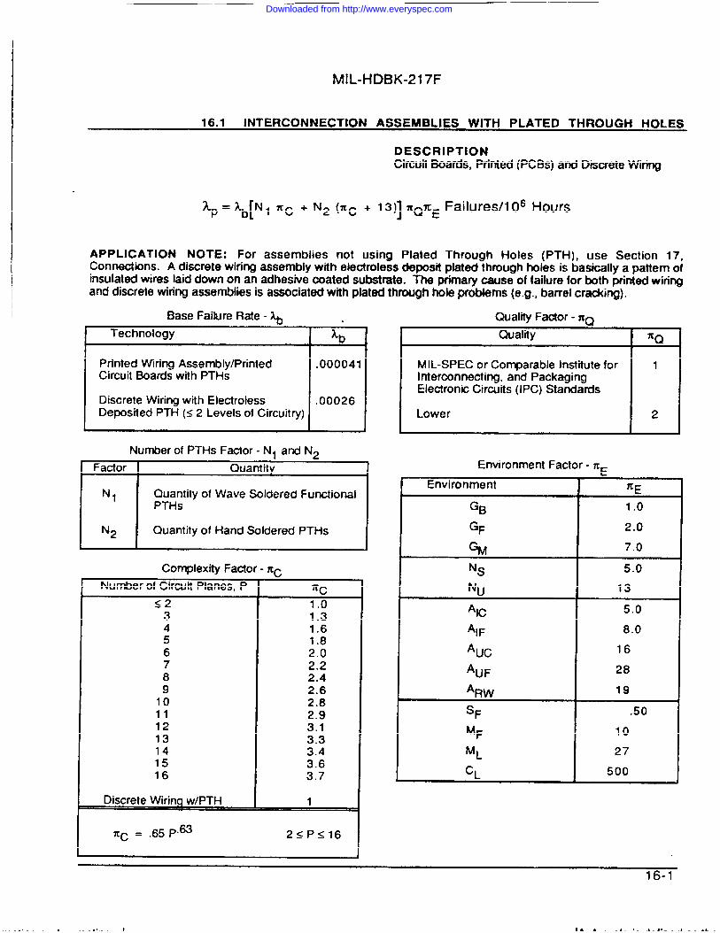
MIL-HDBK-217F
16.1 INTERCONNECTION ASSEMBLIES WITH PLATED THROUGH HOLES
DESCRIPTIONCircuit Boards, Printed (PCBS) and Discrete Wiring
Ap = [Lb N1 xc + N2 (ZC + 13)] ~Q~E Failures/106 Hours
APPLICATION NOTE: For assemblies not using Plated Through Holes (PTH), use Section 17,Connections. A discrete wiring assembly with electrokms deposit plated through holes is basically a pattern ofinsulated wires laid down on an adhesive coated substrate. The primary cause of failure for both printed wiri~and discrete wiring assemblies is associated with plated through kle pr6blems (e.g., barrel cracki~).
Base Failure Rate - ~Technology i~bl
Printed Wiring Assembly/Printed II.000041Circuit Boards with PTHs
Discrete Wiring with Electroless II.00026Deposited PTH (s 2 Levels of Circuitry)
Number of PTHs Factor - N, ard N-&
Factor Quantit~
N, Quantity of Wave Soldered FunctionalPTHs
N2I
Quantity of Hand Soldered PTHs IComplexity Factor - Zn
Number of Circuit Planes, P52345678910111213141516
Discrete Wiring w/PTf-i
Xc = .65 P.m
1.31.61.82.02.22.42.62.82.93.13.33.43.63.7
1
2sPs16
Qud@ ~actor - fiQ
Quality nQ
MIL-SPEC or Comparable Institute for 1Interconnecting, and PackagingElectronic Circuits (lPC) Standards
Lower 2
Environment Factor - nE
I Environment I 7CC
GB
GF
GM
Ns
Nu
AC
‘IF
‘Uc
*UF
‘RWSF
MF
ML
c,
1.0
2.0
7.0
5.0
13
5.0
8.0
16
28
19
.50
10
27
500
Downloaded from http://www.everyspec.com
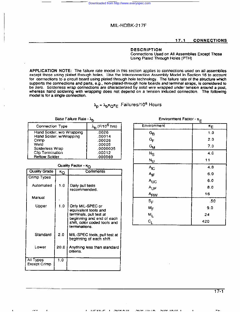
MIL-HDBK-217F
17.1 CONNECTIONS
DESCRIPTIONConnections Used on All Assemblies Except ThoseUsing Plated Through Holes (PTH)
APPLICATION NOTE: The failure rate model in this section applies to connections used on all assembliesexcept those using plated through holes. Use the Interconnection Assembly Model in Section 16 to accountfor connections to a circuit board using plated through hole technology. The failure rate of the structure whichsupports the connections and parts, e.g., non-plated-through hole boards and terminal straps, is considered tobe zero. Solderless wrap connections are characterized by solid wire wrapped under tension around a post,whereas hand soldering with wrapping does not depend on a tension induced connection. The followiWmodel is for a single co~nection. -- -
~ = ~ZQZE Failures/l 06 Hours
Base FaiJure Rate - L!
Connection TypeHand Solder, w/o WrappingHand Solder, w/WrappingCrimpWeldSolderless WrapClip TerminationReflow Solder
u
*.00014.00026.00005.0000035.00012.000069
Quaiiiy Factor - XOQuality Grade ~Q C;mmentsCrimp Types
Automated 1,0 Daily pull testsrecommended.
Manual ●
Upper 1.0 Only MIL-SPEC orequivalent tools andterminals, pull test atbeginning and end of eachshift, color coded tools andterminations.
Standard 2.0 MIL-SPEC tools, pull test atbeginning of each shift.
Lower 20.0 Anything less than standardcriteria.
411Types 1.0~xcept Crimp
Environment Factor - ZF
Environment fiE
GB 1.0
GF 2.0
GM 7.0
N~ 4.0
Nu 11
*IC 4.0
‘IF 6.0
‘Uc 6.0
‘UF 8.0
%w 16
sF .50
MF 9.0
ML 24
CL 420—
17-1
Downloaded from http://www.everyspec.com
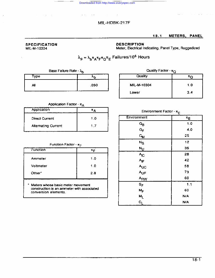
,,
MIL-HDBK-217F
18.1 METERS, PANEL
SPECIFICATION DESCRIPTIONMIL-M-103O4 Meter, Electrical Indicating, Panel Type, Ruggedized
‘P = %nAzFnQzE Failures/l 06 Hours
Base Failure Rate - ~Type
All .090
Application Factor - ~AApplication IDirect Current 1.0
Alternating Current 1.7
Function Factor - ~F
Function 1 ~F
Ammeter 1.0Voltmeter
I1.0
Other* I 2.8
● Meters whose basic meter movementconstruction is an ammeter with associatedconversion elements.
QuaI”@ Factor - ~Quality I nQ
M IL-M-1 0304 1.0
Lower 3.4
Environment Factor - XF
Environment ~E
GB 1.0
GF 4.0
%! 25
Ns 12
Nu 35
Alc 28
‘IF 42
‘Uc 58
‘UF 73
‘RW 60
SF 1,1
MF 60
ML NIA
CL N/A
18-1
Downloaded from http://www.everyspec.com
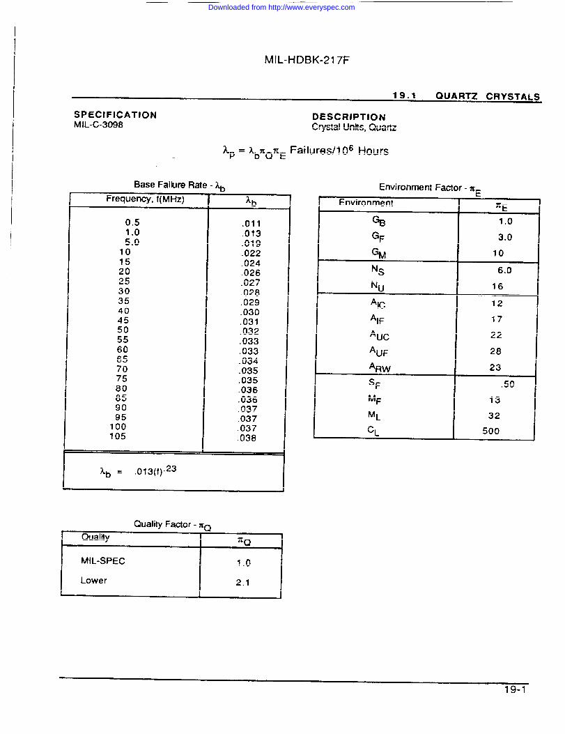
MIL-HDBK-217F
I
I
19.1 QUARTZ CRYSTALS
SPECIFICATION DESCRIPTIONMIL-C-3098 Crystal Units, Quartz
Lp = AbXQnE Failures/l 06 Hours
Base Failure Rate - ~Frequency, f(MHz) I Lk
u
0.5 .0111.0 .0135.0 .01910 .02215 .02420 .02625 .02730 .02835 .02940 .03045 .03150 .03255 .03360 .03365 .03470 .03575 .03580 .03685 .03690 .03795 .037
100 .037105 .038
Ab = .o13(f).23
Quality Factor - xfiu
Quality fiQ
MIL-SPEC 1.0
Lower 2.1
Environment Factor - xcL
Environment ~E
G~ 1.0
GF 3.0GM 10
NS 6.0NU 16
Aic 12
‘iF 17
‘Uc 22
‘UF 28
%w 23
SF .50MF 13ML 32CL 500
19-1
—__—_——_——__—_____ —_—_____
Downloaded from http://www.everyspec.com
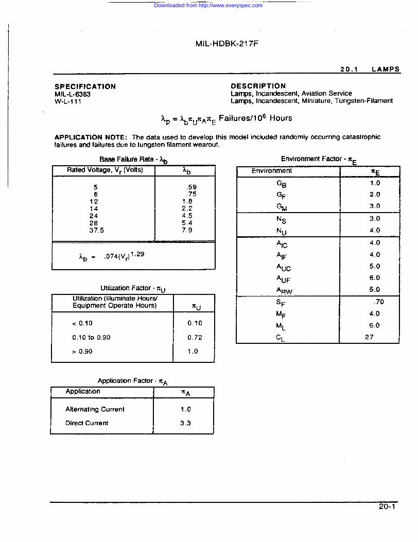
MIL-HDBK-217F
20.1 LAMPS
SPECIFICATIONMIL-L-6363W-L-1 11
APPLICATION
kp =
NOTE: The data used
~~u~A~E Failures/l 06 Hours
to develop this model included randomly occurring catastrophicfailures and failures due to tungsten filament wearout.
Base FaiUre Rate - ~.Rated Voltage, Vr (Votts)
56
1214242837.5
IAb = .074(vr)’ “29
DESCRIPTIONLamps, Incandescent, Aviation SewiceLamps, Incandescent, Miniature, Tungsten-Filament
Ab
.59
.751.82.24.55.47.9
Util@ion Factor- nuUtilization (Illuminate Hour#Equipment Operate Hours)
< 0.10
0.10 to 0.90
> 0.90
Application Factor - ~A
0.10
0.72
1.0
Application
Alternating Current 1.0
Direct Current 3.3
Environment Factor - m~
Environment %E
GB 1.0
GF 2.0
GM 3.0
NS 3.0
Nu 4.0
*IC 4.0
‘IF 4.0
‘Uc 5.0
‘UF 6.0
*RW 5.0
SF .70
MF 4.0
ML 6.0
cL 27
20-1
. a.. I 1 11 I
Downloaded from http://www.everyspec.com
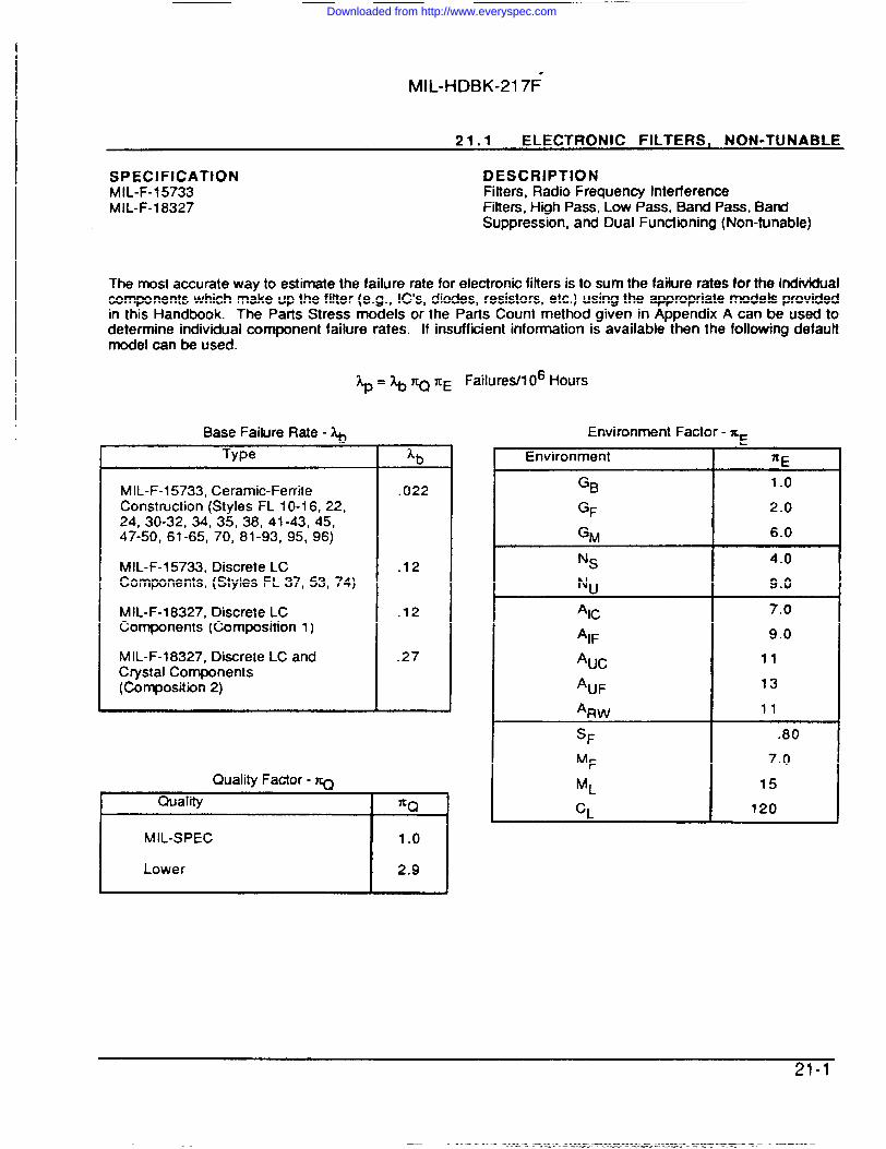
MIL-HDBK-217+
21.1 ELECTRONIC FILTERS, NON-TUNABLE
SPECIFICATION DESCRIPTIONMlL-F-l 5733 Filters, Radio Frequency InterferenceMIL-F-18327 Fitters, High Pass, Low Pass, Band Pass, Band
Suppression, and Dual Functioning (Non-tunable)
The most accurate way to estimate the failure rate for electronic fitters is to sum the failure rates tor the individualcompments which make up the filter (e.g., IC’s, diodes, resistors, etc.) using the appropriate models providedin this Handbook. The Parts Stress models or the Parts Count method given in Appendix A can be used todetermine individual component failure rates. If insufficient information is available then the following defauttmodel can be used.
~=%~xE
Base Failure Rate - ~
Failures/l 06 Hours
Environment Factor - ZEType
MlL-F-l 5733, Ceramic-FerriteConstruction (Styles FL 10-16, 22,24, 30-32, 34, 35, 38, 41-43, 45,47-50, 61-65, 70, 81-93, 95, 96)
MlL-F-l 5733, Discrete LCComponents, (Styles FL 37, 53, 74)
MlL-F-l 8327, Discrete LCComponents (Composltlon 1)
M IL-F-18327, Discrete LC andCfystai Components(Composition 2)
Quality Factor - ~
Ab
.022
.12
.12
.27
I Quality1
MiL-SPEC 1.0
I LowerI
2.9
—Environment ~E
GB 1.0
GF 2.0
GM 6.0
NS 4.0
NU 9.0
*IC 7.0
‘IF 9.0
‘Uc 11
*UF 13
‘RW 11
SF .80
MF 7.0
ML 15
CL 120
21-1
l\ I I — ---- r ndda[
Downloaded from http://www.everyspec.com
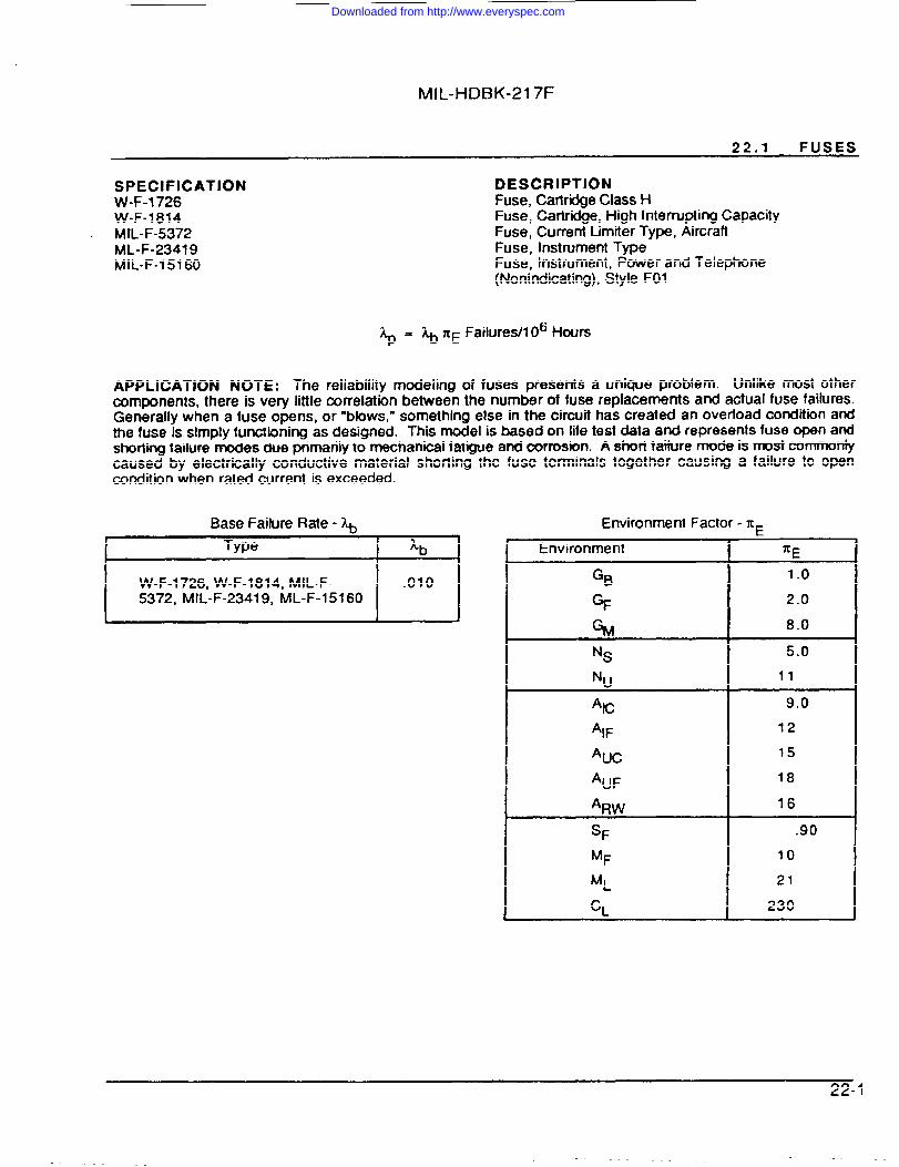
MIL-HDBK-217F
22.1 FUSES
SPECIFICATIONW-F-1726W-F-1814MIL-F-5372ML-F-23419MIL-F-15160
DESCRIPTIONFuse, Caftridge Class HFuse, CaMdge, High Interrupting CapacityFuse, Current Limiter Type, AircraftFuse, Instrument TypeFuse, Instrument, Power and Telephone(Nonindicating), Style FO1
+) “ %‘E‘ai1ure@106‘Wrs
APPLICATION NOTE: The reliability modeling of fuses presents a unique problem. Unlike most othercomponents, there is very little correlation between the number of fuse replacements and actual fuse failures.Generally when a fuse opens, or “blows, - something else in the circuit has created an overload condition andthe fuse is sknply functbning as designed. This model is based on life test data and represents fuse open andshorting failure modes due primarily to mechanical fatigue and corrosion. A short faiture mode is most cornmontycaused by electrically conductive material shorting the fuse terminals together causing a failure to opencondition when rated current is exceeded.
Base Failure Rate - &Type
W-F-1726, W-F-1814, MIL-F- .0105372, MIL-F-23419, ML-F-151 60
Environment Factor - TCF
Environment ~E
% 1.0
GF 2.0
% 8.0
NS 5.0
Nu 11
AC 9.0
‘IF 12
‘Uc 15
*UF 18
*RW 16
SF .90
MF 10
ML 21
CL 230J
22-1
Downloaded from http://www.everyspec.com
I
II MIL-HDBK-217FII
23.1 MISCELLANEOUS PARTS
L - Failure Rates for Miscellaneous Parts (Failure@ 106 Hours)
Vibrators (M IL-V-95)60-cycle120-cycle400-cycle
LampsNeon Lamps
Fiber Optic Cables (Single Fiber Types Only)
Single Fiber O ptic Connectors*
Microwave Elements (Coaxial & Waveguide)Attenuators (Fixed & Variable)
Fixed Elements (Directional Couplers, Fixed Stubs & Cavities)
Variable Elements (Tuned Stubs & Cavities)
Microwave Ferrite DevicesIsolators & Circulators (S100W)
Isolators & Circulators (>100W)
Phase Shifter (Latching)
Dummy Loads< 1Oow
1Oow to <
> 1000W
1Ooow
Terminations (Thin or Thick Film Loads Used in Stripline and ThinFilm Ckcults)
Failure Rate
152040
0.20
0.1 (Per Fiber Km)
0.10
See Resistors, Type RD
Negligible
0.10
0.10x z~
0.20 x ~E
O.10x?tE
0.010 x ~E
0.030 x n~
0.10 x ZE
0.030 x fiE
Caution: Excessive Mating-Demating Cycles May Seriously Degrade Reliability
23-1
Downloaded from http://www.everyspec.com
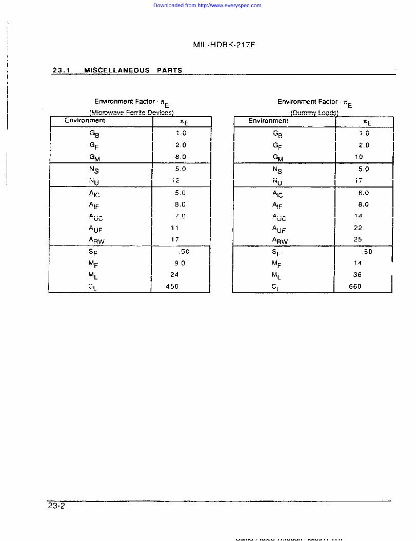
I
MIL-HDBK-217F
23.1 MISCELLANEOUS PARTS —
,.. .V. V..- -v . W.O, .V -w..-””
Environment ~E
GB 1.0
GF 2.0
GM 8.0
NS 5.0
Nu 12
*IC 5.0
‘IF 8.0
‘Uc 7.0
‘UF 11
‘RW 17
SF .50
MF 9.0
ML 24
CL 450 I{
Environment Factor - X-
(Durnmy LoadEnvironment
GB
GF
GM
N~
N“
AC
‘IF
*UC‘UF
*RWSF
MF
ML
c,
kI
1.02.0
10
5.0
17
6.0
8.0
14
22
25
.50
14
36
660
23-2
a
Downloaded from http://www.everyspec.com
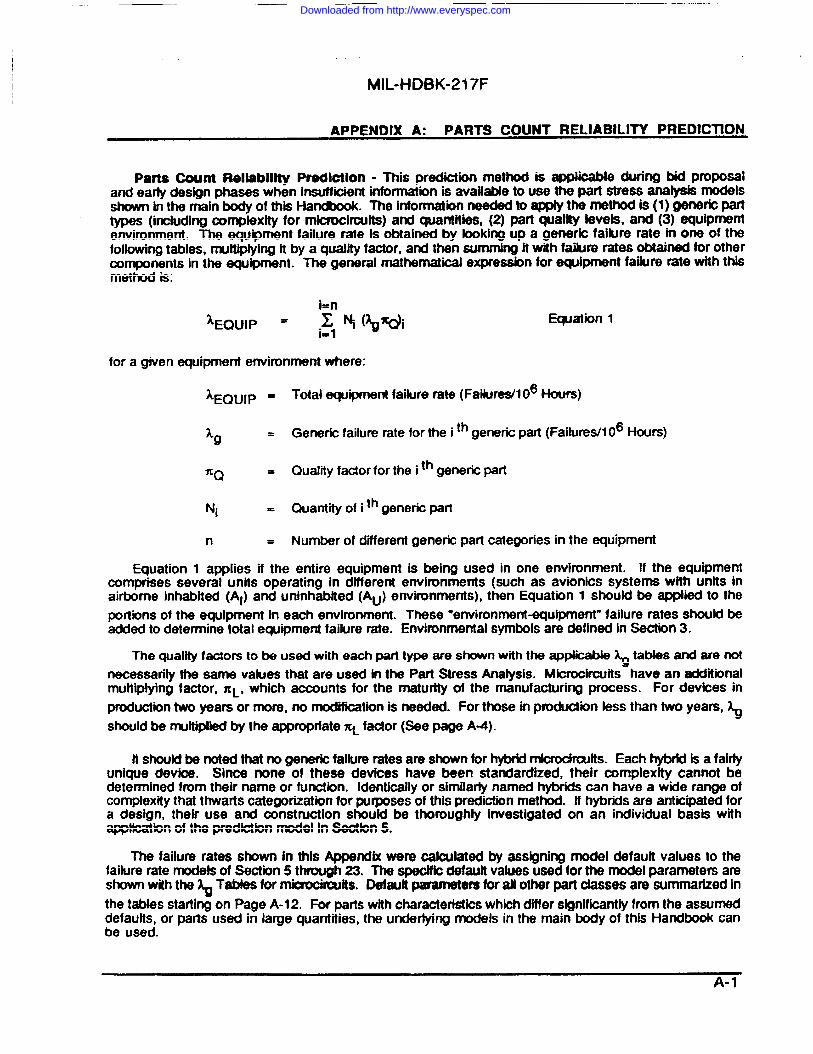
MIL-tiDBK-217F
APPENDIX A: PARTS COUNT RELIABILITY PREDICTtON
Parts Ccxmt Rellablllty Prediction - This prediction method is applicable during bid proposaland early design phases when insuff-kient information is avaitable to use the part stress analysis modelsshown in the rndn body of this Handbook. The information needed to apptythe method is (1) generk palws (includlng complexity for mkrodrcults) and quantities, (2) part quallty levels, and (3) equipmentenvironment. The equipment failure rate Is obtained by looking up a generic failure rate in one of thefollowing tables, muttiptying it by a quality factor,and then summing it with failure rates obtained for othercomponents in the equipment. The general mathematkal expressbn for equipment failure rate with thismethod is:
Equation 1
for a given equipment environment where:
‘EQUIP - Total equipment failure rate (Failure@l 06 Hours)
‘9 = Generic failure rate for the i ‘h generk part (Failures/106 Hours)
7L Q = Quality factor for the i ‘h generic part
Ni = Quantityof i ‘h generk part
n = Number of different generk part categories in the equipment
Equation 1 applies if the entire equipment is being used in one environment. If the equipmentcomprises several units operating in different environments (such as avionics systems with units inairborne inhabited (Al) and uninhabited (Au) environments), then Equation 1 should be applied to theportions of the equipment In each environment. These “environment-equipment” failure rates should beadded to determine total equipment failure rate. Environmental symbols are defined in SeCtion 3.
The quality factors to be used with each part type are shown with the appkabk ~ tables and are notnecessarily the same values that are used in the Parl Stress Anatysis. Microcircuits have an additionalmultiplying factor, ~L, which accounts for the maturfty of the manufacturing process. For devices inproduction two years or more, no rrmdiiition is needed. For those kI production less than two years, ~should be ndtiplied by the appropriate XL factor (see page A-4).
ft should be noted that no generic failure rates are shown for hybrid mkrocimdts. Each hybdd is a fakfyunique devke. Since none of these devkes have been standardized, their complexity cannot bedetermined from their name or function. Identically or similarly named hybrids can have a wide range ofcomplexity that thwarts categorization for pufposes of this prediction method. tf hybrids are anticipated fora design, their use and construction should be thoroughly investigated on an individual basis withapplication of the predktbn model in Section 5.
The failure rates shown In this Appendix wem calculated by assigning model defautt values to thefailure rate modets of Section !5through 23. The speclfk defaultvaJues used for the model parameters areshown with the ~ Tabtes for mkrocimults. Default parameters for atiother part cfasses are summarized inthe tables startifi on Page A-12. For parts with characterfstks which differ significantly from the assumeddefaults, or parls used in large quantities, the underlying models in the main body of this Handbook canbe used.
A-1
Downloaded from http://www.everyspec.com
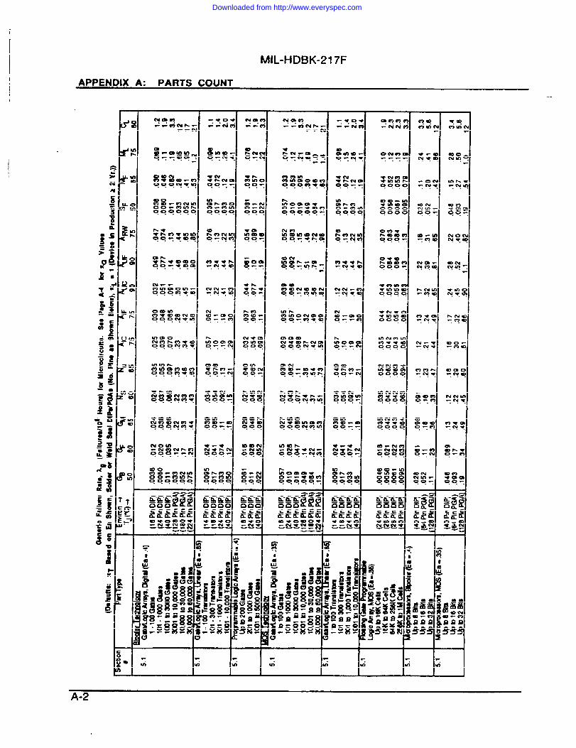
I
MIL-HDBK-217F
APPENDIX A: PARTS COUNT
-*O*. ...mi@j I
Wmlcum.00.
C99$
. .
snNc9tnc9w*a0000 I
ml-meetnm000
Cuu:. . .
:f%mo-mm0000 I
131l–
L●
I*:A-2
-=——--.—-=-———a——-. —-——–—= —. –—–——–———- ————– ——–-= == =. —
Downloaded from http://www.everyspec.com
MIL-HDBK-217F
. .
APPENDIX A: PARTS COUNT
U3
:
&i0
0
o.
o
liniimil~l-_I
H ~-s I
13-LAUL--l!
n I
Downloaded from http://www.everyspec.com
MIL-HDBK-217F
APPENDIX A: PARTS COUNT
II Ifj>+
1
ii —
II I● k(?3”—
0
.-Ss
B
Downloaded from http://www.everyspec.com
MIL-HDBK-217F
APPENDIX A: PARTS COUNT
m .
.
0
1!i!I A
--$?A--
a5 in
A-5
--– M --~+=-=-..--..-- —--- –
Downloaded from http://www.everyspec.com
MIL-HDBK-217F
APPENDIX A: PARTS COUNT
#9
A-6
Downloaded from http://www.everyspec.com
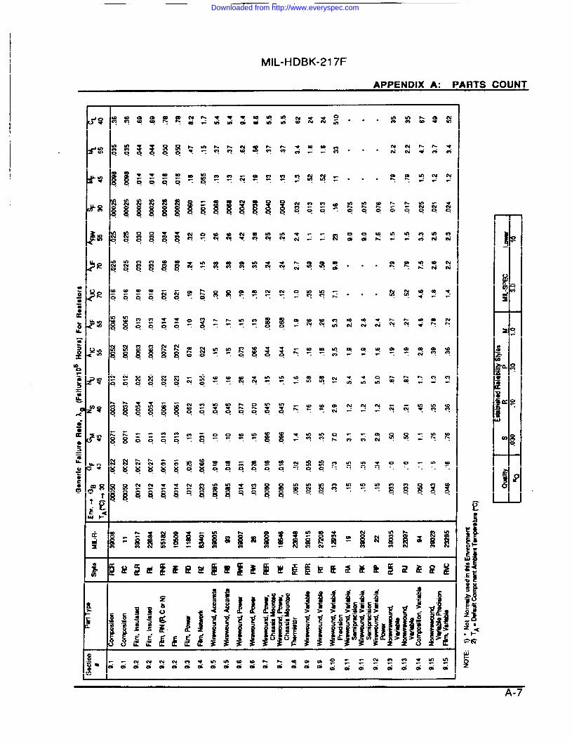
MIL-HDBK-217F
APPENDIX A: PARTS COUNT
A-7
I
Downloaded from http://www.everyspec.com
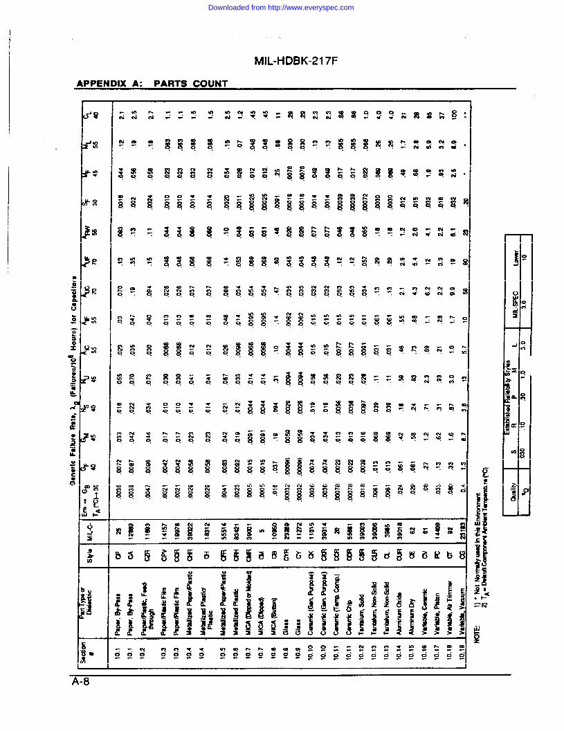
MIL-I+DBK-217F
APPENDIX A: PARTS COUNT
.&
N
0 3
a10
m.
m
* * -
N
0
0
0
N
ij
&8
0
$ *,0,
Downloaded from http://www.everyspec.com
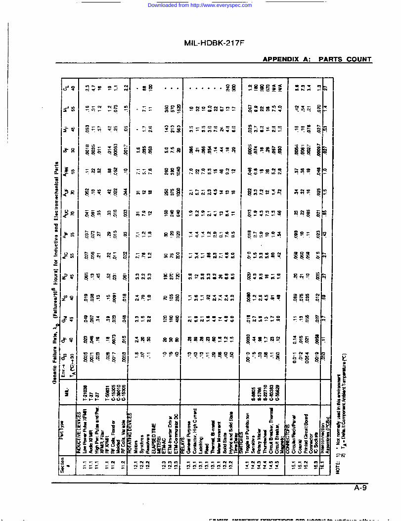
MIL-HDBK-217F
APPENDIX A: PARTS COUNT
A-9
Downloaded from http://www.everyspec.com
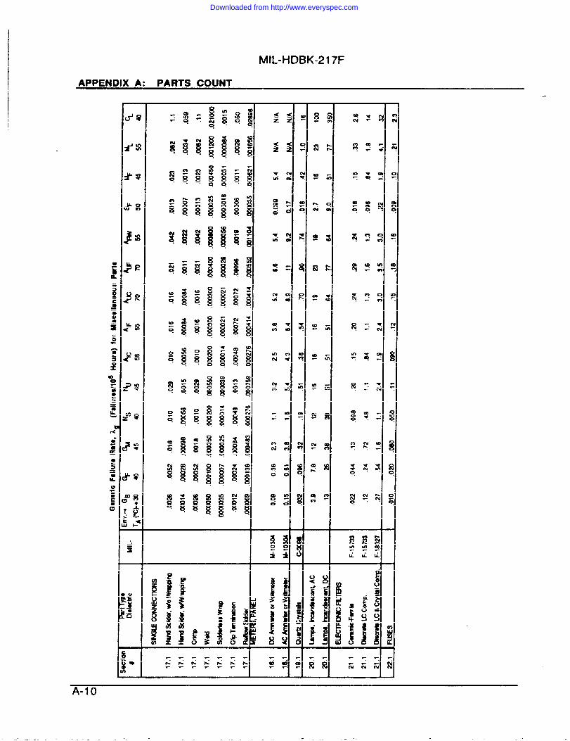
MIL-HDBK-217F
APPENDIX A: PARTS COUNT
m
N
c+
U3
w
m
to
N
N
Q
h“
mF2
.
.
A-10
Downloaded from http://www.everyspec.com
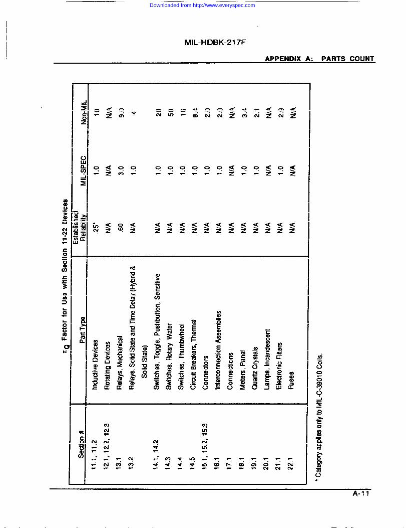
MIL-HDBK-217F
APPENDIX A: PARTS COUNT
oN
o.
*.(9
o .
0Ui
oFi
C&
0d
o .s -
au
.g8
.g
c%ai-d
I C5●
A-II
I 11 1 1 I la I I I
Downloaded from http://www.everyspec.com
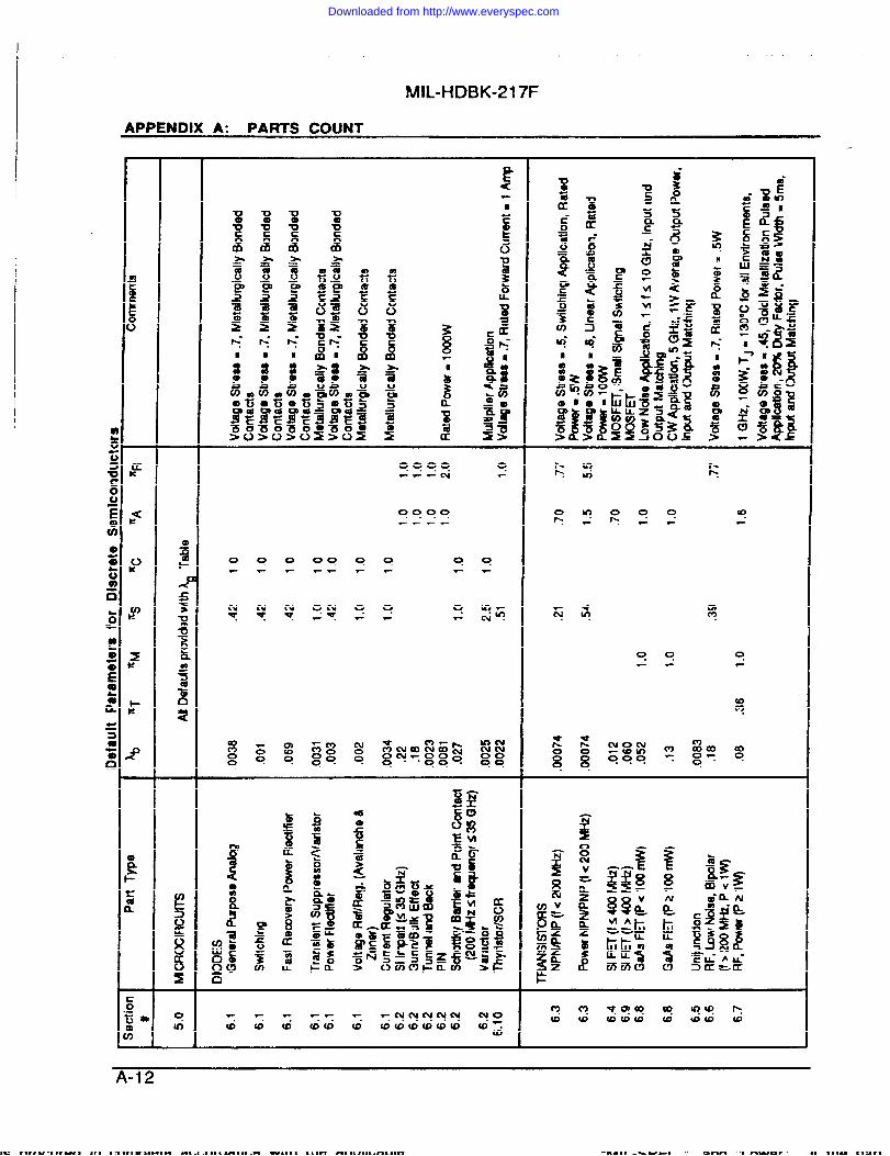
MIL-HDBK-217F
APPENDIX A: PARTS COUNT
0000000 . .FV--T- Y7-
0000. . . .T-- Y-.
w .-
.
a—- U .
Downloaded from http://www.everyspec.com
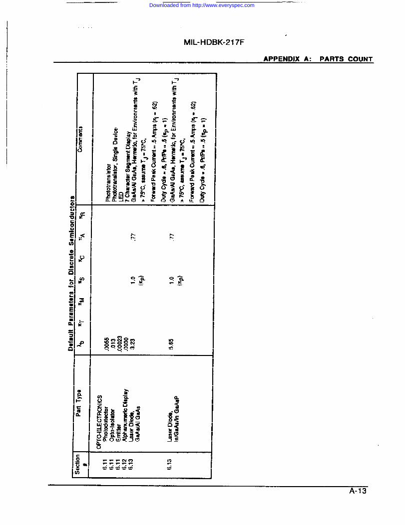
. . .
MIL-HDBK-217F.
APPENDIX A: PARTS COUNT
A-13
Downloaded from http://www.everyspec.com
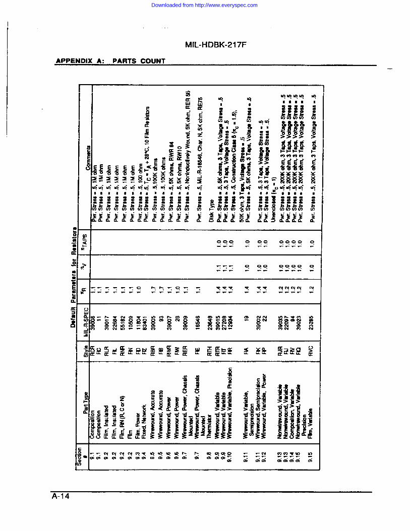
MIL-HDBK-217F
APPENDIX A: PARTS COUNT
A-14
I I m I
Downloaded from http://www.everyspec.com
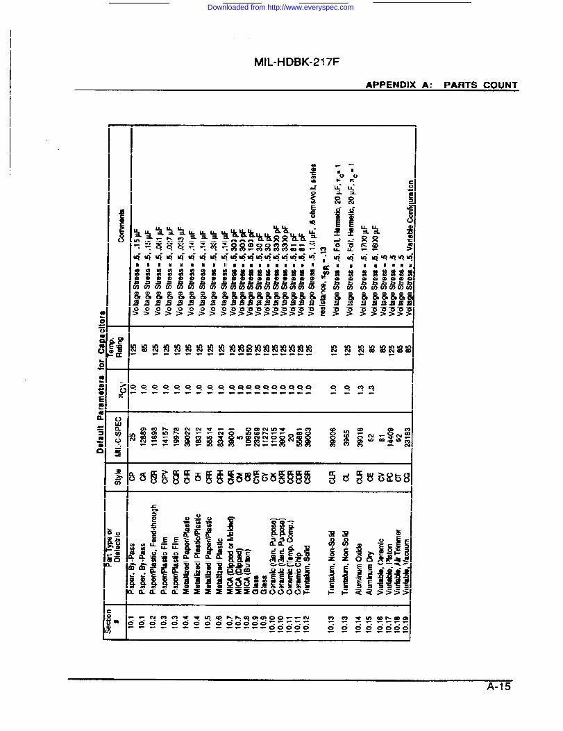
MIL-HDBK-217F
APPENDIX A: PARTS COUNT
? 0.00.0.000.00. qo. o.000ooo o 0 qq---v-- -- -9FW-. .V-WF ----
I I
A-15
I I—-- I
Downloaded from http://www.everyspec.com
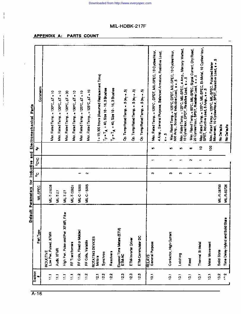
II
MIL-HDBK-217F
APPENDIX A: PARTS COUNT
00 0 0 0.
C9
a5
0
$+
8
U3
m m m.. .
8
.
if
—5‘*i9—
A-16
.1 I-.
Downloaded from http://www.everyspec.com
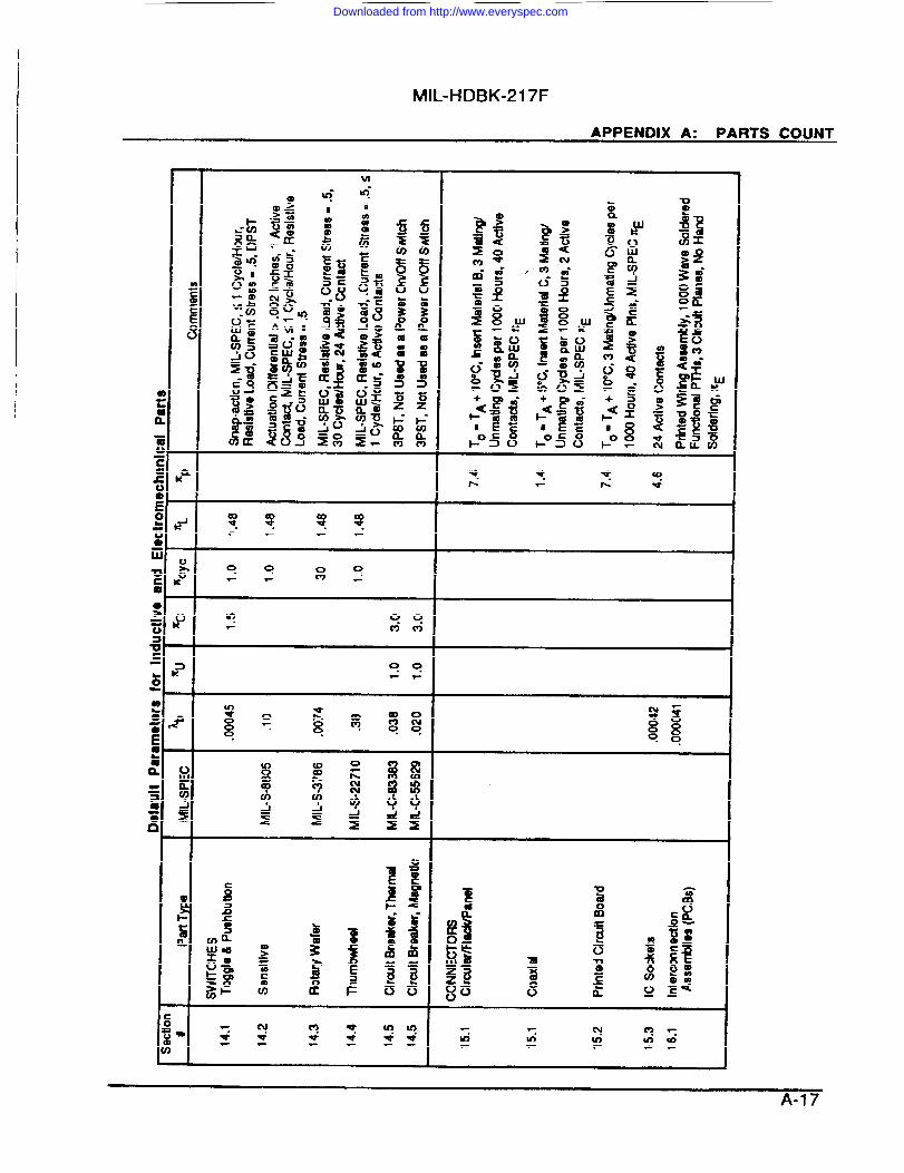
MIL-HDBK-217F
APPENDIX A: PARTS COUNT
A-17
nn I AK
Downloaded from http://www.everyspec.com
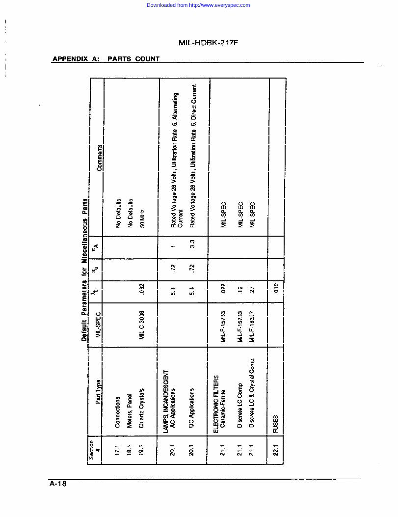
MIL-HDBK-217F
APPENDIX A: PARTS COUNT
/4-18
Downloaded from http://www.everyspec.com
MIL-HDBK-217F
APPENDIX B: VHSJC/VHSIGLIKE AND VLSI CMOS (DETAILED MODEL)
This appendix contains thedetaibd versbn of the VHSICMSI CMOS model contained in Sectbn 5.3. Itis provided to albw more detailed device level design trade-offs to be acxmmplkhed for predominatefailure modes and mechanisms exhibited in CMOS devices. Reference 30 should be consulted for adetailed derivation of this model.
Lp(t)
Ip(t)
Aox(t)
q-Jt)
kc(t)
~~~(t)
kPAC
% SD
q~(t)
The equations for
CN~ RATUSWL
~,(t) + ~t) + ~(t) + ~~(t) + ~.~ + ~~ + ~~(t)
Pred.kted Failure Rate as a Function of Time
Oxide Failure Rate
Metallization Failure Rate
Hot Carner Failure Rate
Contamination Failure Rate
Package Failure Rate
EOS/ESD Failure Rate
Miscellaneous Failure Rate
each of the above failure mechanism failure rates are as follows:
A %YPEO)(
~ )[
-7.7 AToxt* (.0788 e
-7.7 to) (+ox) (eLox (in F/l 06) = AR OR )
.399((
5 2exp ~ In (t + to) - In t500x
+ (t+to)a~x=Ox ) )1
A = Total Chip Area (in cr#)
‘TYPEOX = .~ for Custom and Logic Devices, 1.23 for Memories and Gate Anays
Downloaded from http://www.everyspec.com
MIL-HDBK-217F
APPENDIX B: VHSIC-VHSIC-LIKE AND VLSI CMOS (DETAILED MODEL)
AR
Doox
DR
to
‘Tox
%(-JX
Eox
t500x
~ox
t
.21 cm2
% 2
()Oxide Defect Density (tf unknown, use —
%where X. = 2 w and X~ is the feature
size of the device)
1 Def ect/cm2
Effective Screening Time
(Actual Time of Test (in 106 hrs.)) ● (ATOX (at Junction s~eenjm tern.) (in ~))”
Temperature Acceleration Factor, = exp[ ‘3 - (+ - *)]8.6 I7x1O 5
(where TJ = Tc + 9JCP (in “K))
1-192 (~ -e *)
Maimm power &Jppiy Votbge VDD, divided by the gate oxide thickness (in
MV/cm)
1.3x10²² (QML)ATOX ‘Vex
(in 106 hrs.)
(QML) = 2 if on CNL, .5 if not.
Sgma obtained fmm test data of oxide faibres fmm the same or similar process. Ifnot avaiiable, use a Oox value of 1.
time (in 106 Hours)
B-2
—
Downloaded from http://www.everyspec.com
4
MIL-HDBK-217F
APPENDIX B: VHSIC/VHSIGLIKE AND VLSI CMOS (DETAILED MODEL)
F FQw
[
A %YPEMET ‘OMET ~ 00102 ~-1 “’8 ‘O)(A& = AR ‘R - ,~E~‘(e-’.’8‘TME+ ) 1
+[(,+;fl=e.P[~(l.(t+to)-,.t50METfJ
‘R
‘OMET
‘R
5= Total Chip Area (in cm
= .88 for Custom and Logic Devices, 1.12 for Memory and Gate Arrays
= .21 cm2
2Xo
= Metal Defect Density (tf unknown use (—) where ~ = 2 pm and X~ is the feature size ofx~
the device)
= 1 Defect/cm*
= Temperature Acceleration Factor
= exp[ 8.6;yj0-5 (~ - A)] (TJ =TCASE +,JcP (inOK)~
‘o = Effective Screening Time
=A ‘= (at Screening Ternp
(in 106 hrs.)
(in ‘K)) ● (Actual Scmenhg Tune (in 106 hrs))
t = (QML) .388 ● (Metal Type)50MET
J2 ATME’
(in 106 hrs.)
(QML) = 2 if on QML, .5 if not.
Metal Type = 1 for Al, 37.5 for AI-CU or for A1-Si-Cu
J u The mean absoMe value of Metal Current Density (in 106 Amps/cm2)
a =WT slgrna otXained from test data on electmnigration failures from the same or a similar
process. If this data is not available use cm = 1.
t = time (in 106 hrs.)
B-3
Downloaded from http://www.everyspec.com
MIL-HDBK-217F
APPENDIX B: VHSIGVHSIGUKE AND VLSI CMOS (DETAILED MODEL) —
-.5
(
22 In (t + to) - In t50
%c HC ) 1‘50HC
(QML)3.74XI 0-5 $u Q -2.5=‘THC ‘d () Id
Id
‘sub
%
to
t
%hl
to
t
(QML) = 2 if on QML, .5 if
% [.039= exptic 8.617x10⁻⁵
not
Drain Current at Operating Temperature. If unknown use id = 3.5 e ‘“00’57‘J ‘in ‘K) (WV
Substrate Current at Operating Temperature. If unknown use
Isub = .0058 e ‘-OOWg ‘J (in ‘K) (mA)
sgma derived from test data, if not available use 1.
ATW (at wreening Temp. (in ‘K)) ● (Test Duration in 106 hours)
time (in 106 hrs.)
ATIC)N F~~TlOf!l
.000022 e-.0028 ATCON t--0028 to AT~N e
exp[
-,0- [+ -4$1(where TJ = Tc + 8JCP (in ‘K))
8.617x1O 5
Effective Screening Time
ATmn (at screening junotion temperature (in ‘K)) ● (actual screening time in 106 hrs.)
time (in 106 hrs.)
B-4
Downloaded from http://www.everyspec.com
MIL-t-iDBK-217F
APPENDIX B: VHSIC/VHSIGLIKE AND VLSI CMOS (DETAILED MODEL)
%AC = (.0024 + l.= x 10-5 (spins)) ~ ~ ~T + ~~
fiE = See Section 5.10
7CQ = See Sectbn 5.10
Package Type npT
DtP 1.0Pin Grid May 2.2Chip Carner (Surface MOUM T=hno~y) 4.7
‘PH
%
‘PH
%0Pt+
TA
Package Hermetidty Factor
Ofor Hermetic Packages
399[(-.5- exp
t~~”In(t) -
~PH2In(tsop”))gIfor plastc packages
86x 10-6 exp[
‘2 - (; - *)]8.617x1O 5
ArWent Temp. (in “K)
[ 12.96exp ~
(mL’230[+-+1+(l-DC)(RIi) whereTJ=Tc + eKp On“K)(for example, for 50% Relative Humidity, use RH = .50)
.74
time (in 106 hrs.)
B-5
Downloaded from http://www.everyspec.com
MIL-HDBK-217F
APPENDIX B: VHSIGVHSIGLIKE AND VLSI CMOS (DETAILED MODEL)
-.0002 VTH%0s = “““ - “OOo:;&-
VTH = ESD Threshold of the device using a 100 pF, 1500 ohm discharge model
‘MIS = (.01 e -2.2 ATMIS t,‘2.2 ~) ~ATMl~ ) (e
‘TMIS = Temperature Acceleration Factor
[
-.423= exp8.6317x10-5 (+ - A)]
where TJ = Tc + eJcP (in ‘K)
to = Effective Screening Time
= ATMl~ (at Screening Terrp (in “K)) ● Actual Screening Time (in 106 hours)
t= time (in 106 hrs.)
B-6
I 7 -an 1 AC
Downloaded from http://www.everyspec.com
MIL-HDBK-217F
APPENDIX C: BIBLIOGRAPHY
Publications tisted with “AD” nunbers may be obtained trom:
National Technical hlfOtiiOfl Service5285 Port Royal Road~@eM, VA 22151(703) 487-4650
U.S. Defense Contractors may obtain copies from:
Defense Technical Information CenterCameron Station - FDA, Bldg. 5Alexandria, VA 22304-6145(703) 274-7633
Documents with AD number prefix with the letter “B” or with the suffix “L”: These documents are in a“Limfted Distributbn” category. Contact the Defense Technical Information Center for_procedures.
Copies of MIL-STDS’S, MIL-HDBK’s, and specifications are available from:
Standardization Document Order Desk700 Robins Ave.Buikfing 4, Section DPhiladelphia, PA 19111-5094(215) 697-2667
The year of publiition of the Rome Laboratory (RL) (formerly Rome Air Development Center (RADC))documents is part of the RADC (or FL) nunber, e.g., RADGTR-66-97 was published in 1968.
1.
2.
3.
4.
5.
6.
7.
8.
9.
10.
11,
“Laser Reliability Prediction,” RADC-TR-75-21 O, AD A016437.
“ReliabiMy Model for Miniature Blower Motors Per MIL-B-23071 B,” RADC-TR-75-178, AD A013735.
‘High Power Microwave Tube Reliability Study,” FAA-RD-76-I 72, AD AO033612.
“Electric Motor Reliabii~ Model,” RADC-TR-77406, AD A0501 79.
“Development of Nonelectronic Part Cyclic Failure Rates,”RADC-TR-77417, AD A050678.
This study devebped new faiture rate models for relays, switches, and connectors.
“Passive Device Failure Rate Models for MIL-HDBK-217B,” RADC-TR-~432, AD A050180.
This study developed new failure rate models for resistors, capacitors and inductive devices.
“Quantification of Printed Circuit Boatd Connector ReWMtty,” RADC-TR-77-433, AD A049980.
“Crimp Connection Reliability,” RADC-TR-78-15, AD A050505.
“LS1/Micmprocessor Reliabilii Prediction Model Development,” RADC-TR-79-97, AD A06891 1.
“A Re@nda~ Notebook,” RADC-TR-77-287, AD A050837.
“Revision of Environmental Faofors for MIL-HDBK-217B,” RADC-TR-80-299, AD A091837.
L-1
.—
Downloaded from http://www.everyspec.com
MIL-HDBK-217F
APPENDIX C: BIBLIOGRAPHY
12.
13.
14.
15.
16.
17.
18.
19.
20.
21.
22.
23.
24.
25.
Traveling Wave Tube Failure Rates,- RADC-TR-80-288, AD A096055.
“Reliability Predict&n Modeling of blew Devices, - RADC-TR~237, AD A090029.
This study devebped failure rate nmdek for magnetic bubble memories and charge~upkfmernortes.
“Failure Rates for Fiber Optic Assemblies,” RADC-TR-80-322, AD A092315.
“Printed Wiring Assembly and Interconnection ReliabMfy,” RADC-TR-81 -318, AD Al 11214.
This study dwebped faihn fate modets for printed wtrfng asae~s, solderless wrapassanbfies, wrapped and soldered assemblies and discrete wirfng assemblies withebctroless depostted plated through holes.
“Avionio Etimentat F_ for MIL-HOBK-21 7,” RADC-TR-81 -374, AD B084430L.
“RADC Thermal Guide for Reliability Engineers,” RADC-TR-82-1 72, AD Al 18839.
“Reliability Modeling of Critical Electronic Devices,” RADC-TR-83-1 08, AD Al 35705.
This report devebped failure rate prediction procedures for magnetrons, vidicions, cathoderay tubes, semiconductor lasers, helium-cadtim lasers, heiiim-neon lasers, Nd: YAG lasers,electronic filters, sofid state relays, time delay relays (electronic hybrid), circuit breakers, I.C.Sockets, thumbwheel switches, electromagnetic meters, fuses, crystals, incandescent lamps,neon gbw lamps and surface acoustic wave devices.
This study developed failure rate models for nonoperating periods.
“RADC Nonelectronic Reliability Notebook,” RADC-TR-85-194, AD A163900.
This report contains failure rate data on rnechanicaf and electromechanical parts.
“Reliabilii Prediction for Spacecraft,” RADC-TR-85-229, AD A149551.
TMs study kwestigated the reliability performance h@ories of 300 Satellite vehicles and is thebasis for the halving of all model %E factors forMIL-HDBK-217E to MIL-HDKB-21 7E, Notice 1.
“Surface Mount Technology: A Reliability Review; 1986, Available from Reliabilii Anatysis Center,PO BOX 4700, Rome, NY 13440-8200, 800-526-4802.
‘Thermal Resktames of Joint Army Navy (JAN) Certified Microcimuif Pa&ages,” RADC-TR46-97,AD B1084I7.
“Large Scale Memory Emr Detection and Correction? RADC-TR-87-92, AD B1 17785L.
This study developed models to cakwlate memory system reliiility for memoriesincorporating error detecting and correcting codes. For a summary of the study see 1989IEEE ReliabiMy and Maintainability SymposUm Proceedings, page 197, “Accounting for SoftErrors in Memory Reliability Prediiion.a
“Reliability Analysis of a Surface Mounted Package Using Finite Element Simulation,” RADC-TR-87-177, AD A189488.
c-2
Downloaded from http://www.everyspec.com

MIL-HDBK-217F
APPENDIX C: BIBLIOGRAPHY
26.
27.
28.
29.
30.
31.
32.
33.
34.
35.
36.
“VHSIC Impact on System Reliability,” RADC-TR-86-13, AD B122629.
“Reliability Assessment of Surface Mount Technology,” RADC-TR-68-72, AD A193759.
“Reliability Prediction Models for Discrete Semiconductor Devices, - RADC-TR-88-97, AD A200529.
This study developed new failure rate prediction modets for GaAs Power FETS, TransientSuppressor Diodes, Infrared LEDs, Diode Array Displays and Current Regulator D-.
“Inqxmt of Fiber Optics on System Reliability and Maintainabilii,” RADC-TR-88-124, AD A2CH946.
“VHSWVHSIC Like Rel&bi14y Prediotlon Modeling,” RADGTR-69-I 71, AD A214601.
This study provides the basis for the VHSIC model appearing in MIL-HDBK-21 7F, Section 5.
“Reliability Assessment Using Finite Element Techniies,m RADC-TR-89-281, AD A21 6907.
This study addresses surface mounted solder interconnections and miorowire board’s plated-thru-hole (PTH) connections. The report gives a detailed account of the factors to beconsidered when performing an FEA and the procedure used to transfer the results to areliability figure-of-merit.
“Reliability Analysis/Assessment of Advanced Technologies,” RADC-TR-90-72, ADA 223647,
This study provides the basis for the revisedmicmchwit models (except VHSIC and BubbleMemories) appearing in MIL-HDBK-217F, Sectii 5.
“Improved Reliability Prediction Model for Field-Access Magnetic Bubble Devices,” AFWAL-TR-81-1052,
“Reliability/Desgn Thermal Applications,” MIL-HDBK-251.
“NASA Parts Application Handbook,” MIL-HDBK-976-B (NASA).This handmok is a five vohnne series which dfscusses a full range of eiectrfcal, electronic andelectromechanical component parts. It provides extensive detailed technical informatbn foreach component part such as: definitions, oonstructbn details, operating characteristics,derating, failure mechanisms, screening techniques, standard parts, environmentalconsiderations, and circuit appliition.
‘Nonelectronic Parts Reliability Data 1991 ,“ NPRD-91.TM report contains field ?aiture rate data on a variety of ektrical, mechanical,electromechanical and microwave parts and assernblii (1400 different part types). It isavailable from the Re@bMty AnaJysis Center, PO Box 4700, Rome, NY 13440-6200, Phone:(315) 337-0900.
Custodians: Preparing Activity:Amy-CR Air Force -17Navy - ECAir Fome -17 Project No. RELI-0064
c-3
. ——---- . .. .
Downloaded from http://www.everyspec.com
I
MIL-HDBK-217F
APPENDIX C: BIBLIOGRAPHY
Review AcWtWs:Army - Ml, AV, ERNavy - Sl+, AS, OS~rForce -11, 13, 14, 15, 18,
19,99
User Activities:Army - AT, ME, GLNavy - CG, MC, YD, TDAlr Force -85
I
c-4
.
Downloaded from http://www.everyspec.com
ImE:ThistcummaynottJe uso d*=7wt*d doaunsm,norbrupostwdvus, ddatkm, udwikatkmofspedk=bn~smQmult cm- Camnoms sdlmbdanmsbfmtinat Oons$mworhplyuthofizdcm mwdvearlypodtJndthodsr9ncdcka8naw8)wbamsnd mnu a ctd nquhm9nts.
(Fo#dahg lt?ishe)
(FM abng this line)
DEPARTMENT OF THE AIR ~E
111111\ n
N OPOSTAGERUERSS NECESSARYGrWfissAFB, NY 13441-5700 IF MAILED
IN THEUNITED STATES
OFFKXAL BUSINESSt331ALTYFOR PRtVATEUSE S300 l~S =LY MAIL
FRSTCtASS W- tm. - w~m D.c.Am~=
Rome laboratoryAlTN: RIJERSSGriffiss AFB, NY 13441-5700
... . . , . .
Downloaded from http://www.everyspec.com
STANDARDIZATION DOCUMENT IMPFtOVEhtENT PROPOSAL(set? hstructbn - I?eveme Ski@
1.
Parag~ Nuntxw and Wording:
Wording
ReaaodRaIionab \ or R~rnrnerKMon :
—•1
c1
ability PnWidon of Electronic E@pment. m m)
DMAMJFAcnmE.R
6. REMARKS
‘a
b Ss (s-a my,St-, ZP
DD .% 1426 PREVIOUS EDfTION IS OBSUETE
Downloaded from http://www.everyspec.com
Related Documents