NJIT ECE 271 Dr. Serhiy Levkov Topic 9 - 1 Topic 9 MOS Memory and Storage Circuits ECE 271 Electronic Circuits I

NJIT ECE 271 Dr. Serhiy Levkov Topic 9 - 1 Topic 9 MOS Memory and Storage Circuits ECE 271 Electronic Circuits I.
Dec 19, 2015
Welcome message from author
This document is posted to help you gain knowledge. Please leave a comment to let me know what you think about it! Share it to your friends and learn new things together.
Transcript
NJIT ECE 271 Dr. Serhiy Levkov Topic 9 - 1
Topic 9 MOS Memory and Storage Circuits
ECE 271
Electronic Circuits I

NJIT ECE 271 Dr. Serhiy Levkov Topic 9 - 2
Chapter Goals
• Overall memory chip organization• Static memory circuits using the six-transistor cell• Dynamic memory circuits• Sense amplifier circuits used to read data from memory
cells• Learn about row and address decoders• Implementation of CPU registers via flip-flops• Pass transistor logic• Read Only Memory
NJIT ECE 271 Dr. Serhiy Levkov Topic 9 - 3
Memory Types
• Read Only Memory (ROM) refers to memory in a digital system that has only read capabilities. Can be used to perform logic operations.
• Random Access Memory (RAM) refers to memory in a digital system that has both read and write capabilities. Mostly it’s a high speed temporary storage memory.
• Static RAM (SRAM) is able to store its information as long as power is applied, and it does not lose the data during a read cycle (early memory was mostly SRAM)
• Dynamic RAM (DRAM) uses a capacitor to temporarily store data which must be refreshed periodically to prevent information loss, and the data is lost in most DRAMs during the read cycle
• SRAM takes approximately four times the silicon area of DRAM with the same technology.
• Digital systems also include usually high speed small size memory – registers to temporarily store information used in operations.
• The memory chip usually includes the storage cells, address decoders - logical circuits for selecting and accessing a particular cell, and sense amplifiers for amplifying the signal retrieved from a cell.
NJIT ECE 271 Dr. Serhiy Levkov Topic 9 - 4
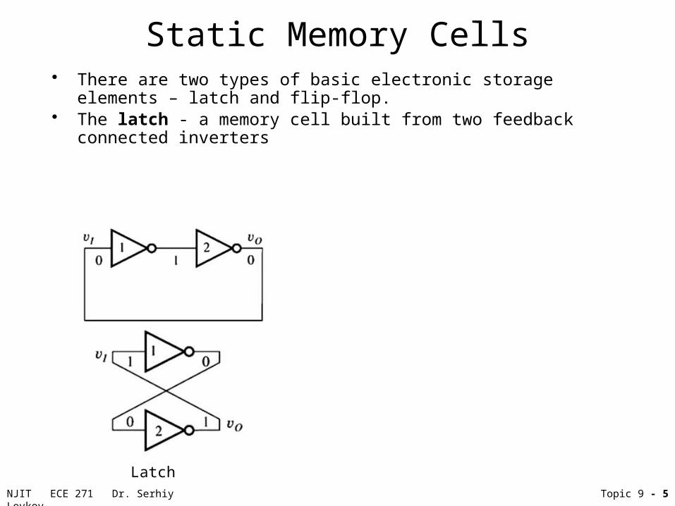
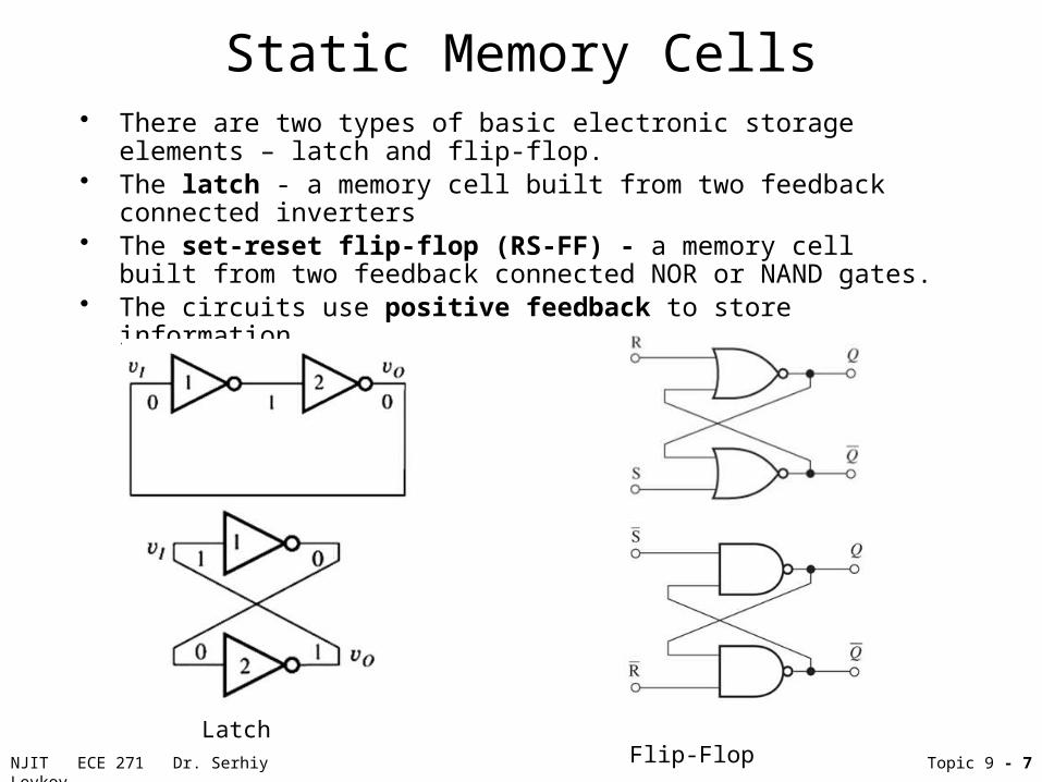
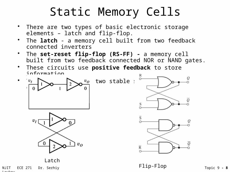
Static Memory Cells• There are two types of basic electronic storage elements – latch and flip-flop.
NJIT ECE 271 Dr. Serhiy Levkov Topic 9 - 5
Static Memory Cells• There are two types of basic electronic storage elements – latch and flip-flop.• The latch - a memory cell built from two feedback connected inverters
Latch

NJIT ECE 271 Dr. Serhiy Levkov Topic 9 - 6
Static Memory Cells• There are two types of basic electronic storage elements – latch and flip-flop.• The latch - a memory cell built from two feedback connected inverters• The set-reset flip-flop (RS-FF) - a memory cell built from two feedback
connected NOR or NAND gates.
Latch Flip-Flop
NJIT ECE 271 Dr. Serhiy Levkov Topic 9 - 7
Static Memory Cells• There are two types of basic electronic storage elements – latch and flip-flop.• The latch - a memory cell built from two feedback connected inverters• The set-reset flip-flop (RS-FF) - a memory cell built from two feedback
connected NOR or NAND gates.• The circuits use positive feedback to store information.
Latch Flip-Flop
NJIT ECE 271 Dr. Serhiy Levkov Topic 9 - 8
Static Memory Cells• There are two types of basic electronic storage elements – latch and flip-flop.• The latch - a memory cell built from two feedback connected inverters• The set-reset flip-flop (RS-FF) - a memory cell built from two feedback
connected NOR or NAND gates.• These circuits use positive feedback to store information.• These circuits have two stable states – bistable circuits.
Latch Flip-Flop
NJIT ECE 271 Dr. Serhiy Levkov Topic 9 - 9
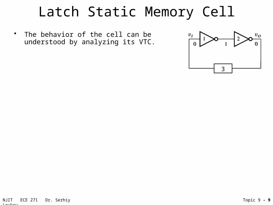
Latch Static Memory Cell
• The behavior of the cell can be understood by analyzing its VTC.
3

NJIT ECE 271 Dr. Serhiy Levkov Topic 9 - 10
Latch Static Memory Cell
• The behavior of the cell can be understood by analyzing its VTC.
• Blue curve is the VTC of the two cascaded inverters 1 and 2.
3

NJIT ECE 271 Dr. Serhiy Levkov Topic 9 - 11
Latch Static Memory Cell
• The behavior of the cell can be understood by analyzing its VTC.
• Blue curve is the VTC of the two cascaded inverters 1 and 2.
• The red line (slope=1) is the VTC of the unit feedback 3.
3
NJIT ECE 271 Dr. Serhiy Levkov Topic 9 - 12
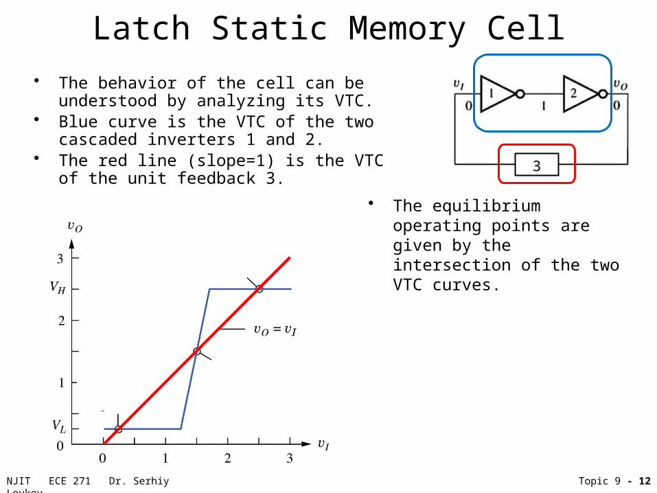
Latch Static Memory Cell
• The equilibrium operating points are given by the intersection of the two VTC curves.
• The behavior of the cell can be understood by analyzing its VTC.
• Blue curve is the VTC of the two cascaded inverters 1 and 2.
• The red line (slope=1) is the VTC of the unit feedback 3.
3
NJIT ECE 271 Dr. Serhiy Levkov Topic 9 - 13
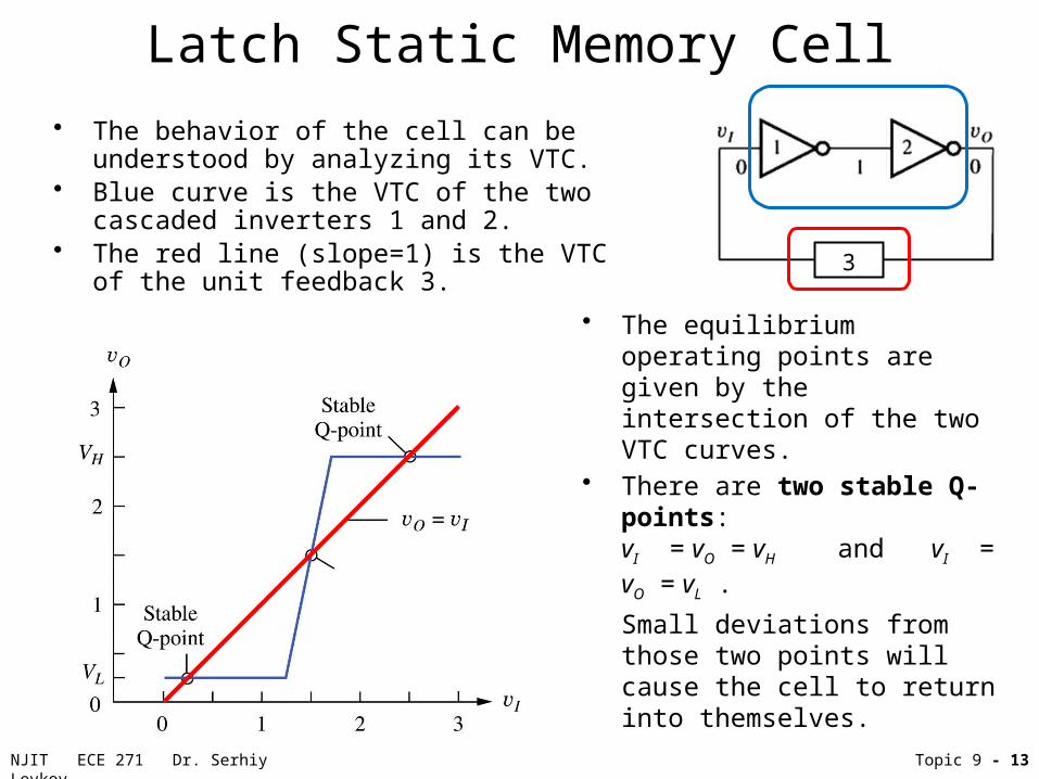
Latch Static Memory Cell
• The equilibrium operating points are given by the intersection of the two VTC curves.
• There are two stable Q-points: vI = vO = vH and vI = vO = vL .
Small deviations from those two points will cause the cell to return into themselves.
• The behavior of the cell can be understood by analyzing its VTC.
• Blue curve is the VTC of the two cascaded inverters 1 and 2.
• The red line (slope=1) is the VTC of the unit feedback 3.
3
NJIT ECE 271 Dr. Serhiy Levkov Topic 9 - 14
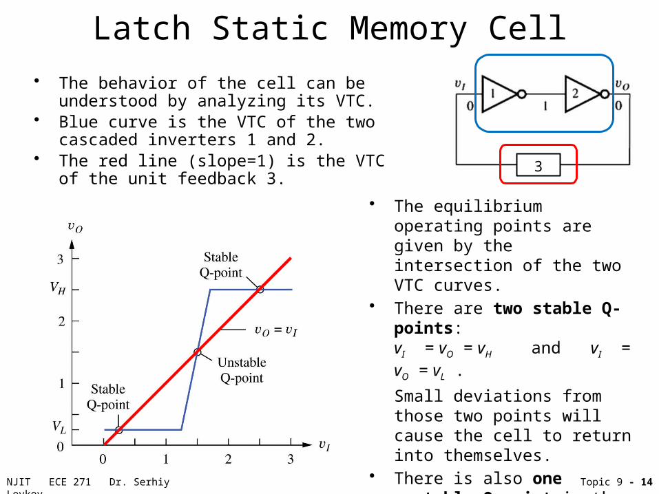
Latch Static Memory Cell
• The equilibrium operating points are given by the intersection of the two VTC curves.
• There are two stable Q-points: vI = vO = vH and vI = vO = vL .
Small deviations from those two points will cause the cell to return into themselves.
• There is also one unstable Q-point in the middle, where slight changes in the voltage will cause it to latch in one of the stable states
• The behavior of the cell can be understood by analyzing its VTC.
• Blue curve is the VTC of the two cascaded inverters 1 and 2.
• The red line (slope=1) is the VTC of the unit feedback 3.
3

NJIT ECE 271 Dr. Serhiy Levkov Topic 9 - 15
The 6-T Cell• The previous cell can exist indefinitely long in one of the stable states – high
or low, i.e. it can store one bit of information – 0 or 1. • However this construction is not yet usable because there is no mechanism to
change the state - to “write” the information into sell.

NJIT ECE 271 Dr. Serhiy Levkov Topic 9 - 16
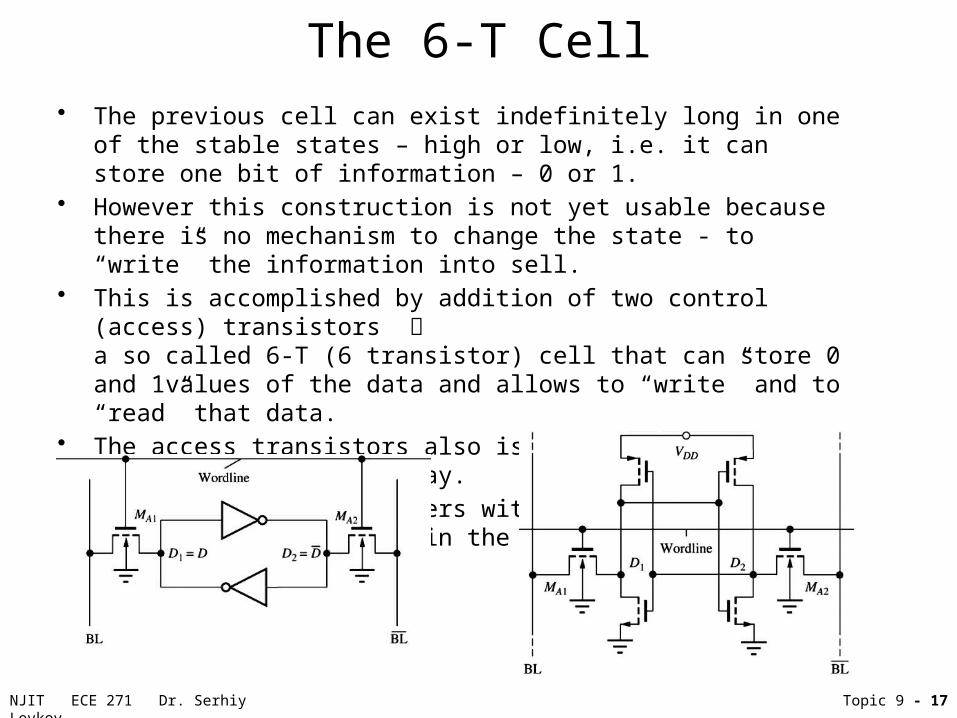
The 6-T Cell• The previous cell can exist indefinitely long in one of the stable states – high
or low, i.e. it can store one bit of information – 0 or 1. • However this construction is not yet usable because there is no mechanism to
change the state - to “write” the information into sell. • This is accomplished by addition of two control (access) transistors
a called 6-T (6 transistor) cell that can store 0 and 1values of the data and allows to “write” and to “read” that data.
• The access transistors also isolate one cell from another in a memory array.
NJIT ECE 271 Dr. Serhiy Levkov Topic 9 - 17
The 6-T Cell• The previous cell can exist indefinitely long in one of the stable states – high
or low, i.e. it can store one bit of information – 0 or 1. • However this construction is not yet usable because there is no mechanism to
change the state - to “write” the information into sell. • This is accomplished by addition of two control (access) transistors
a so called 6-T (6 transistor) cell that can store 0 and 1values of the data and allows to “write” and to “read” that data.
• The access transistors also isolate one cell from another in a memory array.• Substituting the inverters with their CMOS representation, we obtain the
circuit implementation of the 6-T SRAM cell.

NJIT ECE 271 Dr. Serhiy Levkov Topic 9 - 18
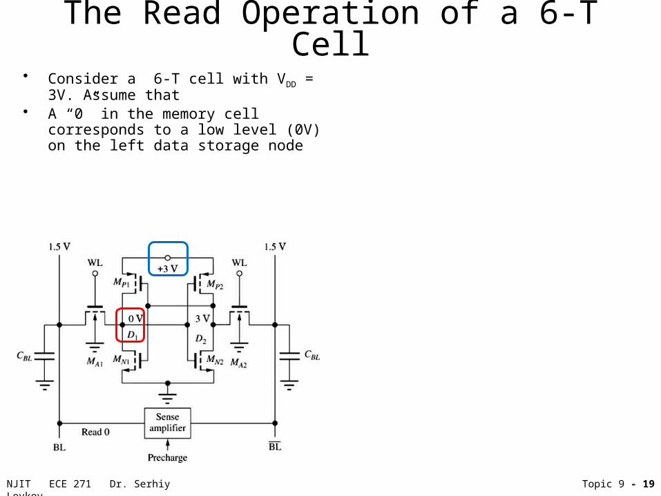
The Read Operation of a 6-T Cell• Consider a 6-T cell with VDD = 3V.
NJIT ECE 271 Dr. Serhiy Levkov Topic 9 - 19
The Read Operation of a 6-T Cell• Consider a 6-T cell with VDD = 3V. Assume that• A “0” in the memory cell corresponds to a low
level (0V) on the left data storage node
NJIT ECE 271 Dr. Serhiy Levkov Topic 9 - 20
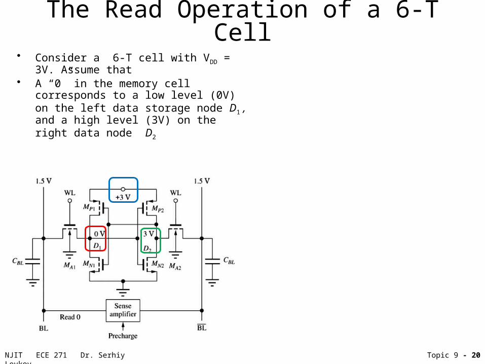
The Read Operation of a 6-T Cell• Consider a 6-T cell with VDD = 3V. Assume that• A “0” in the memory cell corresponds to a low
level (0V) on the left data storage node D1 , and a high level (3V) on the right data node D2

NJIT ECE 271 Dr. Serhiy Levkov Topic 9 - 21
The Read Operation of a 6-T Cell• Consider a 6-T cell with VDD = 3V. Assume that• A “0” in the memory cell corresponds to a low
level (0V) on the left data storage node D1 , and a high level (3V) on the right data node D2
• A “1” in the memory cell corresponds to a high level on D1 , and a low level on D2 .

NJIT ECE 271 Dr. Serhiy Levkov Topic 9 - 22
The Read Operation of a 6-T Cell
“0”
WL=0 WL=0
Initial state of the cell storing a “0” with the bitlines’ initially precharged to VDD/2 and WL set to 0.
• Consider a 6-T cell with VDD = 3V. Assume that• A “0” in the memory cell corresponds to a low
level (0V) on the left data storage node D1 , and a high level (3V) on the right data node D2
• A “1” in the memory cell corresponds to a high level on D1 , and a low level on D2 .

NJIT ECE 271 Dr. Serhiy Levkov Topic 9 - 23
The Read Operation of a 6-T Cell
WL=0 WL=0
Initial state of the cell storing a “0” with the bitlines’ initially precharged to VDD/2 and WL set to 0.
WL=0 WL=0
“0” “0”
• Consider a 6-T cell with VDD = 3V. Assume that• A “0” in the memory cell corresponds to a low
level (0V) on the left data storage node D1 , and a high level (3V) on the right data node D2
• A “1” in the memory cell corresponds to a high level on D1 , and a low level on D2 .

NJIT ECE 271 Dr. Serhiy Levkov Topic 9 - 24
The Read Operation of a 6-T CellTo read the data we set WL to 3V, • Consider a 6-T cell with VDD = 3V. Assume that
• A “0” in the memory cell corresponds to a low level (0V) on the left data storage node D1 , and a high level (3V) on the right data node D2
• A “1” in the memory cell corresponds to a high level on D1 , and a low level on D2 .
WL=0 WL=0
Initial state of the cell storing a “0” with the bitlines’ initially precharged to VDD/2 and WL set to 0.
“0” “0”
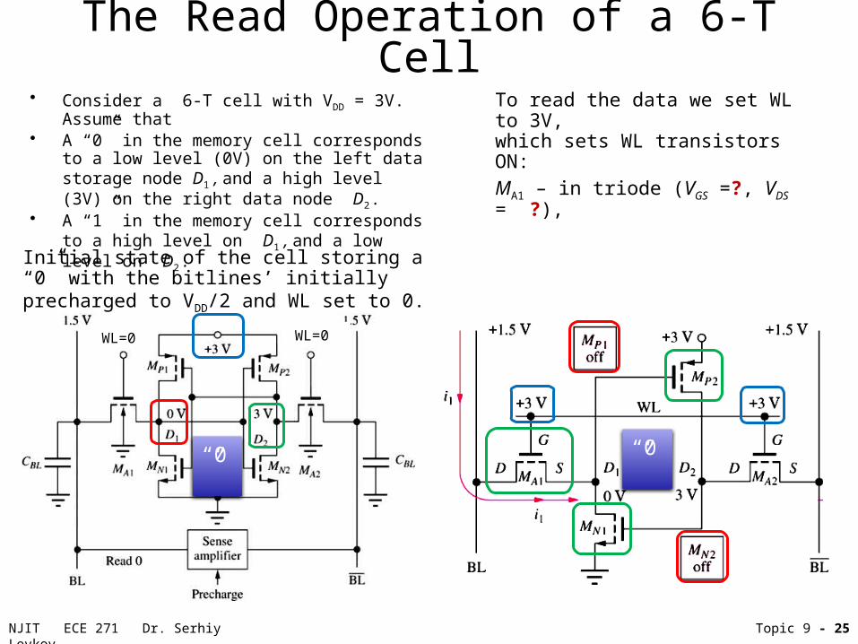
NJIT ECE 271 Dr. Serhiy Levkov Topic 9 - 25
The Read Operation of a 6-T Cell
WL=0 WL=0
Initial state of the cell storing a “0” with the bitlines’ initially precharged to VDD/2 and WL set to 0.
To read the data we set WL to 3V,which sets WL transistors ON:
MA1 – in triode (VGS =?, VDS = ?),
• Consider a 6-T cell with VDD = 3V. Assume that• A “0” in the memory cell corresponds to a low level
(0V) on the left data storage node D1 , and a high level (3V) on the right data node D2 .
• A “1” in the memory cell corresponds to a high level on D1 , and a low level on D2 .
“0” “0”
NJIT ECE 271 Dr. Serhiy Levkov Topic 9 - 26
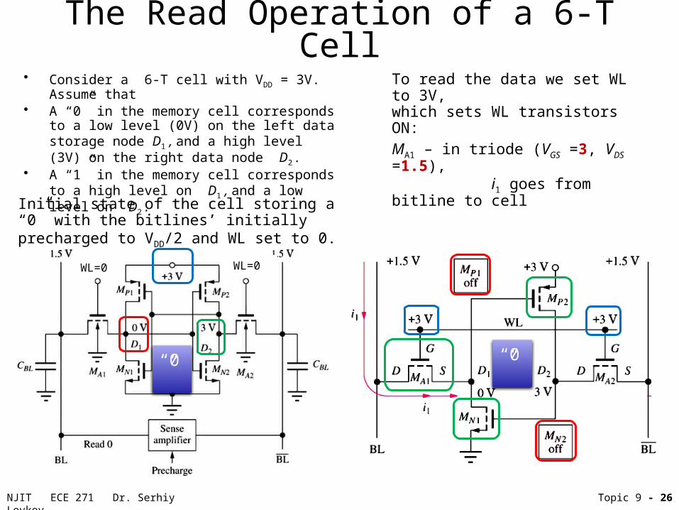
The Read Operation of a 6-T Cell
WL=0 WL=0
Initial state of the cell storing a “0” with the bitlines’ initially precharged to VDD/2 and WL set to 0.
To read the data we set WL to 3V,which sets WL transistors ON:
MA1 – in triode (VGS =3, VDS =1.5), i1 goes from bitline to cell
• Consider a 6-T cell with VDD = 3V. Assume that• A “0” in the memory cell corresponds to a low level
(0V) on the left data storage node D1 , and a high level (3V) on the right data node D2 .
• A “1” in the memory cell corresponds to a high level on D1 , and a low level on D2 .
“0” “0”

NJIT ECE 271 Dr. Serhiy Levkov Topic 9 - 27
The Read Operation of a 6-T Cell
WL=0 WL=0
Initial state of the cell storing a “0” with the bitlines’ initially precharged to VDD/2 and WL set to 0.
To read the data we set WL to 3V,which sets WL transistors ON:
MA1 – in triode (VGS =3, VDS =1.5), i1 goes from bitline to cell
MA2 – in saturation (VGS = ? , VDS = ? ),
• Consider a 6-T cell with VDD = 3V. Assume that• A “0” in the memory cell corresponds to a low level
(0V) on the left data storage node D1 , and a high level (3V) on the right data node D2 .
• A “1” in the memory cell corresponds to a high level on D1 , and a low level on D2 .
“0” “0”
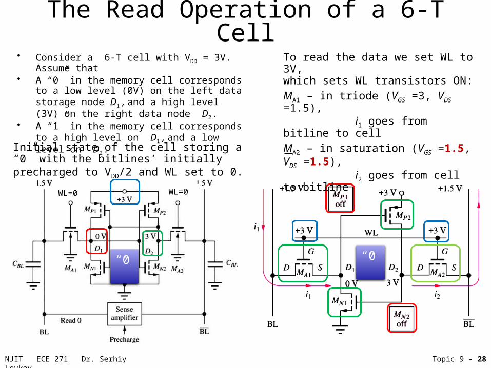
NJIT ECE 271 Dr. Serhiy Levkov Topic 9 - 28
The Read Operation of a 6-T Cell
WL=0 WL=0
Initial state of the cell storing a “0” with the bitlines’ initially precharged to VDD/2 and WL set to 0.
To read the data we set WL to 3V,which sets WL transistors ON:
MA1 – in triode (VGS =3, VDS =1.5), i1 goes from bitline to cell
MA2 – in saturation (VGS =1.5, VDS =1.5), i2 goes from cell to bitline
• Consider a 6-T cell with VDD = 3V. Assume that• A “0” in the memory cell corresponds to a low level
(0V) on the left data storage node D1 , and a high level (3V) on the right data node D2 .
• A “1” in the memory cell corresponds to a high level on D1 , and a low level on D2 .
“0” “0”

NJIT ECE 271 Dr. Serhiy Levkov Topic 9 - 29
The Read Operation of a 6-T Cell
WL=0 WL=0
Initial state of the cell storing a “0” with the bitlines’ initially precharged to VDD/2 and WL set to 0.
To read the data we set WL to 3V,which sets WL transistors ON:
MA1 – in triode (VGS =3, VDS =1.5), i1 goes from bitline to cell
MA2 – in saturation (VGS =1.5, VDS =1.5), i2 goes from cell to bitline
Currents i1 and i2 are sensed by sense amplifier, which helps to set BL to 0V and BL to 3V.
• Consider a 6-T cell with VDD = 3V. Assume that• A “0” in the memory cell corresponds to a low level
(0V) on the left data storage node D1 , and a high level (3V) on the right data node D2 .
• A “1” in the memory cell corresponds to a high level on D1 , and a low level on D2 .
“0” “0”

NJIT ECE 271 Dr. Serhiy Levkov Topic 9 - 30
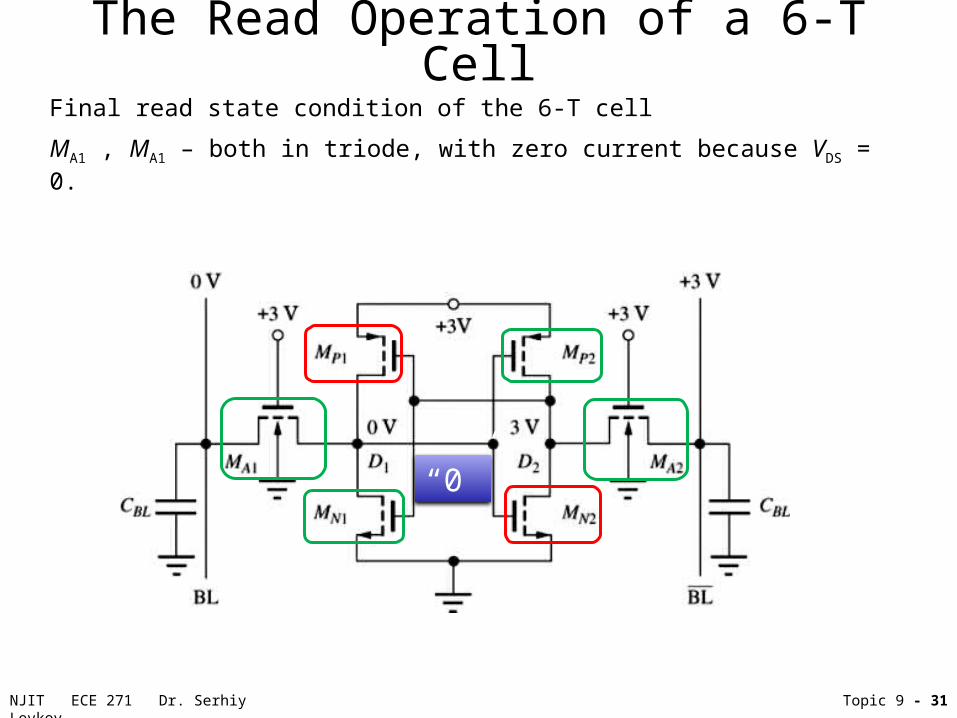
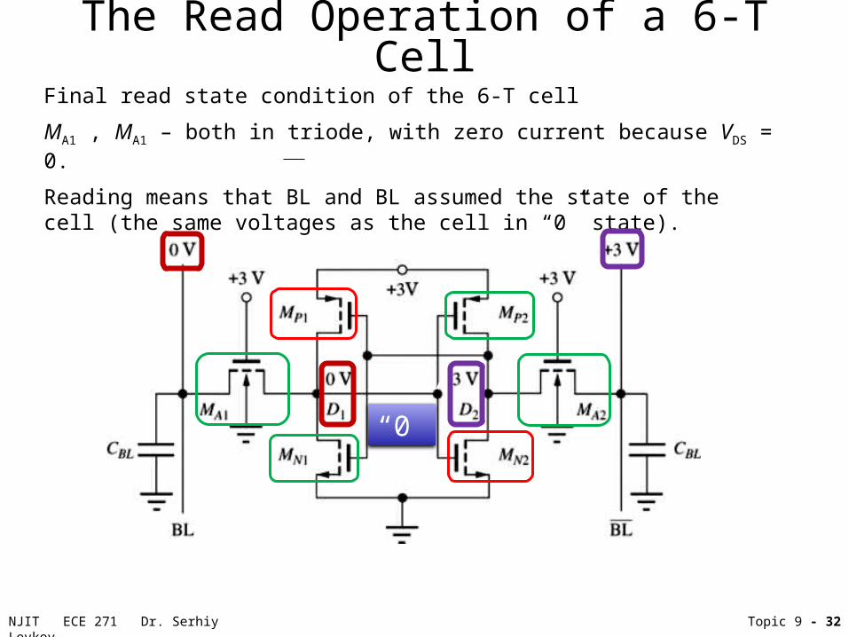
The Read Operation of a 6-T CellFinal read state condition of the 6-T cell
“0”
NJIT ECE 271 Dr. Serhiy Levkov Topic 9 - 31
The Read Operation of a 6-T CellFinal read state condition of the 6-T cell
MA1 , MA1 – both in triode, with zero current because VDS = 0.
“0”
NJIT ECE 271 Dr. Serhiy Levkov Topic 9 - 32
The Read Operation of a 6-T CellFinal read state condition of the 6-T cell
MA1 , MA1 – both in triode, with zero current because VDS = 0.
Reading means that BL and BL assumed the state of the cell (the same voltages as the cell in “0” state).
“0”

NJIT ECE 271 Dr. Serhiy Levkov Topic 9 - 33
The Read Operation of a 6-T Cell
At t =1ns the precharge of 1.5V is removed.
At t =1ns the worldline begins transition from 0 to 3V.
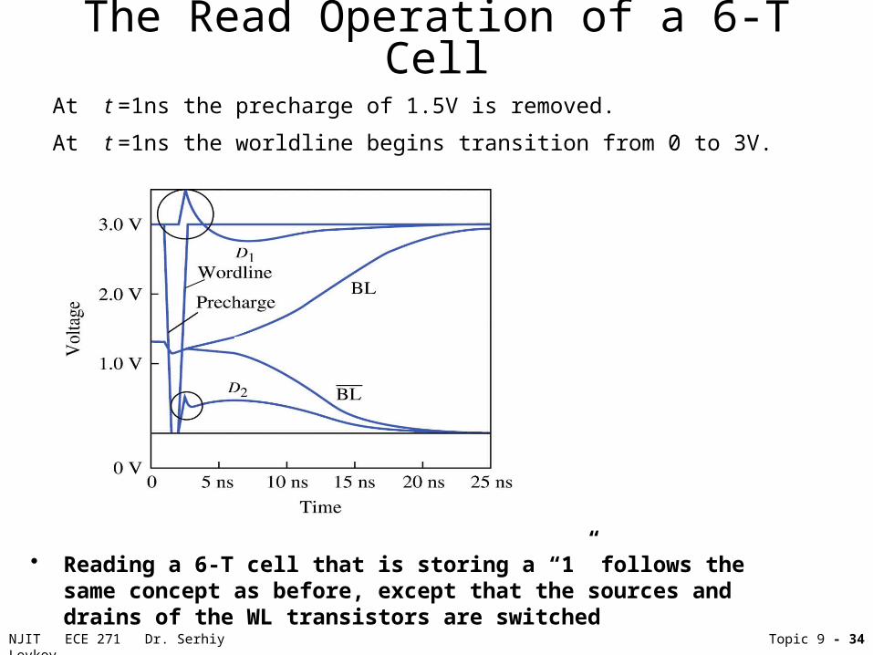
NJIT ECE 271 Dr. Serhiy Levkov Topic 9 - 34
The Read Operation of a 6-T Cell
At t =1ns the precharge of 1.5V is removed.
At t =1ns the worldline begins transition from 0 to 3V.
• Reading a 6-T cell that is storing a “1” follows the same concept as before, except that the sources and drains of the WL transistors are switched
NJIT ECE 271 Dr. Serhiy Levkov Topic 9 - 35
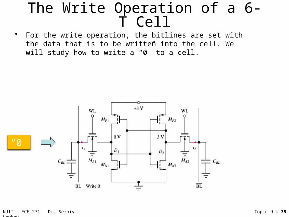
The Write Operation of a 6-T Cell• For the write operation, the bitlines are set with the data that is to be written
into the cell. We will study how to write a “0” to a cell.
“0”
NJIT ECE 271 Dr. Serhiy Levkov Topic 9 - 36
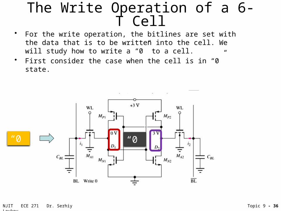
The Write Operation of a 6-T Cell• For the write operation, the bitlines are set with the data that is to be written
into the cell. We will study how to write a “0” to a cell.• First consider the case when the cell is in “0” state.
“0” “0”
NJIT ECE 271 Dr. Serhiy Levkov Topic 9 - 37
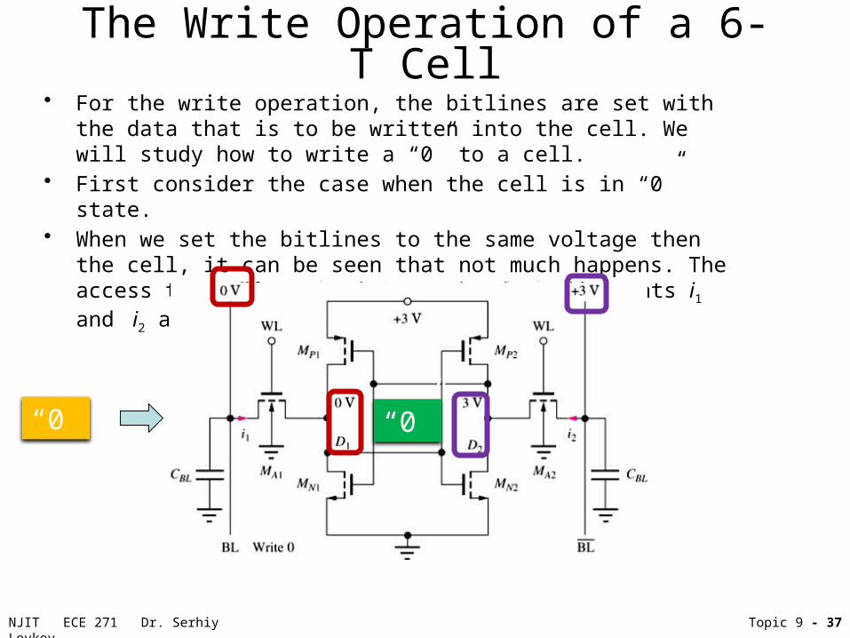
The Write Operation of a 6-T Cell• For the write operation, the bitlines are set with the data that is to be written
into the cell. We will study how to write a “0” to a cell.• First consider the case when the cell is in “0” state.• When we set the bitlines to the same voltage then the cell, it can be seen that
not much happens. The access transistors have VDS = 0 and the currents i1 and i2 are also zero.
“0” “0”

NJIT ECE 271 Dr. Serhiy Levkov Topic 9 - 38
The Write Operation of a 6-T Cell• Now lets consider writing a “0” to a cell that is storing a “1”.
“0” “1”
WLWL

NJIT ECE 271 Dr. Serhiy Levkov Topic 9 - 39
The Write Operation of a 6-T Cell• Now lets consider writing a “0” to a cell that is storing a “1”. • The writing begins with setting worldline to 3V.
“0” “1”
NJIT ECE 271 Dr. Serhiy Levkov Topic 9 - 40
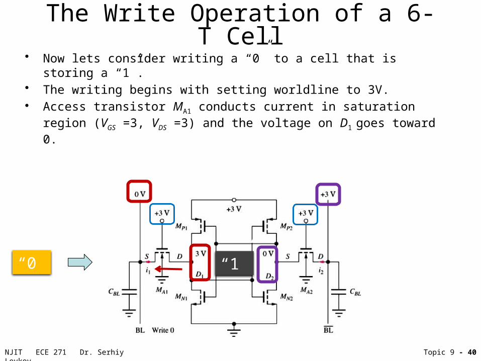
The Write Operation of a 6-T Cell• Now lets consider writing a “0” to a cell that is storing a “1”. • The writing begins with setting worldline to 3V.• Access transistor MA1 conducts current in saturation region (VGS =3, VDS =3) and
the voltage on D1 goes toward 0.
“0” “1”

NJIT ECE 271 Dr. Serhiy Levkov Topic 9 - 41
The Write Operation of a 6-T Cell• Now lets consider writing a “0” to a cell that is storing a “1”. • The writing begins with setting worldline to 3V.• Access transistor MA1 conducts current in saturation region (VGS =3, VDS =3) and
the voltage on D1 goes toward 0.
• Access transistor MA2 also conducts current in saturation region (VGS =3, VDS =3) and the voltage on D2 goes toward (3- VTN).
“0” “1”
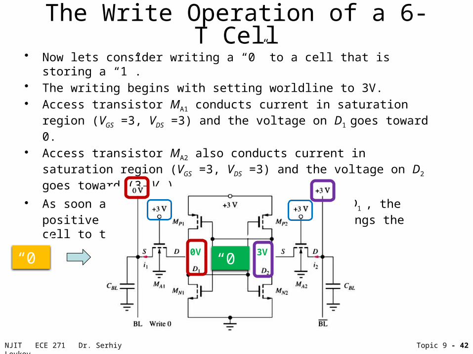
NJIT ECE 271 Dr. Serhiy Levkov Topic 9 - 42
The Write Operation of a 6-T Cell• Now lets consider writing a “0” to a cell that is storing a “1”. • The writing begins with setting worldline to 3V.• Access transistor MA1 conducts current in saturation region (VGS =3, VDS =3) and
the voltage on D1 goes toward 0.
• Access transistor MA2 also conducts current in saturation region (VGS =3, VDS =3) and the voltage on D2 goes toward (3- VTN).
• As soon as voltage on D2 exceeds voltage on D1 , the positive feedback takes over and quickly brings the cell to the new state (D1 =0 , D2 =1) .
“0” 0V 3V“0”
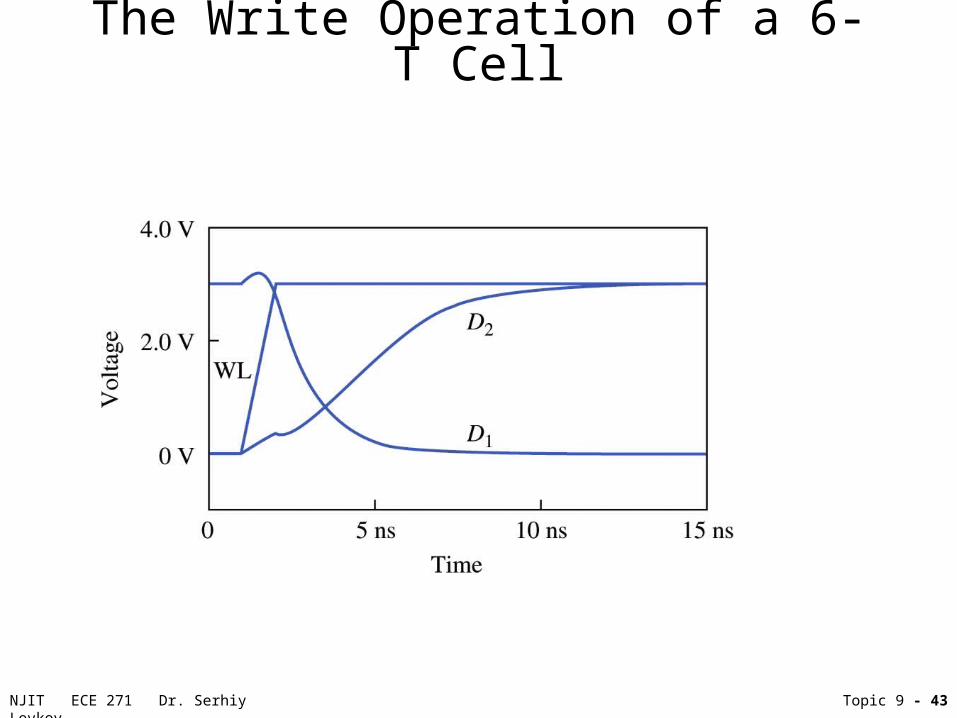
NJIT ECE 271 Dr. Serhiy Levkov Topic 9 - 43
The Write Operation of a 6-T Cell

NJIT ECE 271 Dr. Serhiy Levkov Topic 9 - 44
Dynamic Memory Cells• In the static memory cell, the data can be stored indefinitely as long as power is
applied.• The pay for this convenience is the amount of transistors -- 6 per cell. • If we drop this requirements, we can create a dynamic memory cell with one
transistor -- the 1-T cell, which uses a capacitor as a storage element, where data is represented as either a presence or absence of a charge (below)
• However, due to leakage currents in MA, the data will eventually be lost, hence it needs to be refreshed (read and then written back) periodically.

NJIT ECE 271 Dr. Serhiy Levkov Topic 9 - 45
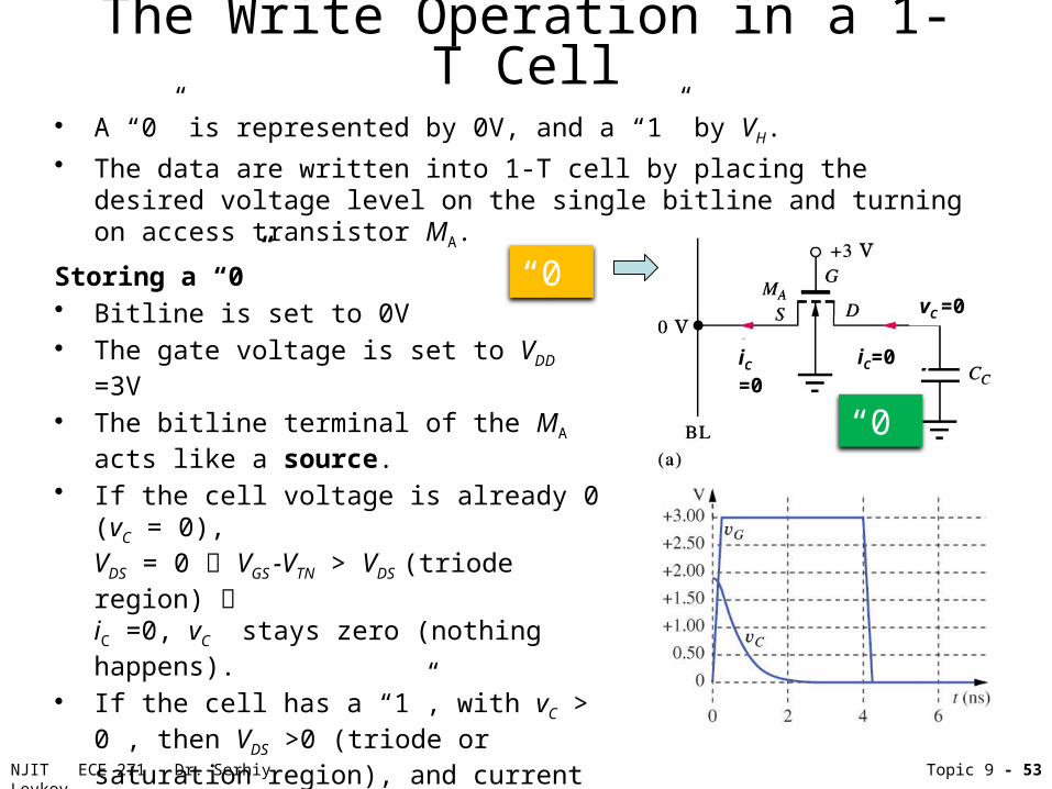
Data Storage in a 1-T Cell
• A “0” is represented by 0V, and a “1” by VH.
• The data are written into 1-T cell by placing the desired voltage level on the single bitline and turning on access transistor MA.

NJIT ECE 271 Dr. Serhiy Levkov Topic 9 - 46
The Write Operation in a 1-T Cell
• A “0” is represented by 0V, and a “1” by VH.
• The data are written into 1-T cell by placing the desired voltage level on the single bitline and turning on access transistor MA.
Storing a “0” “0”
NJIT ECE 271 Dr. Serhiy Levkov Topic 9 - 47
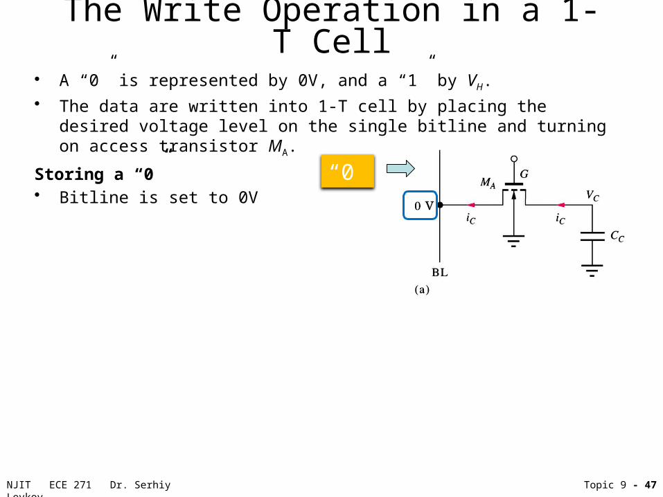
• A “0” is represented by 0V, and a “1” by VH.
• The data are written into 1-T cell by placing the desired voltage level on the single bitline and turning on access transistor MA.
Storing a “0”• Bitline is set to 0V
“0”
The Write Operation in a 1-T Cell
NJIT ECE 271 Dr. Serhiy Levkov Topic 9 - 48
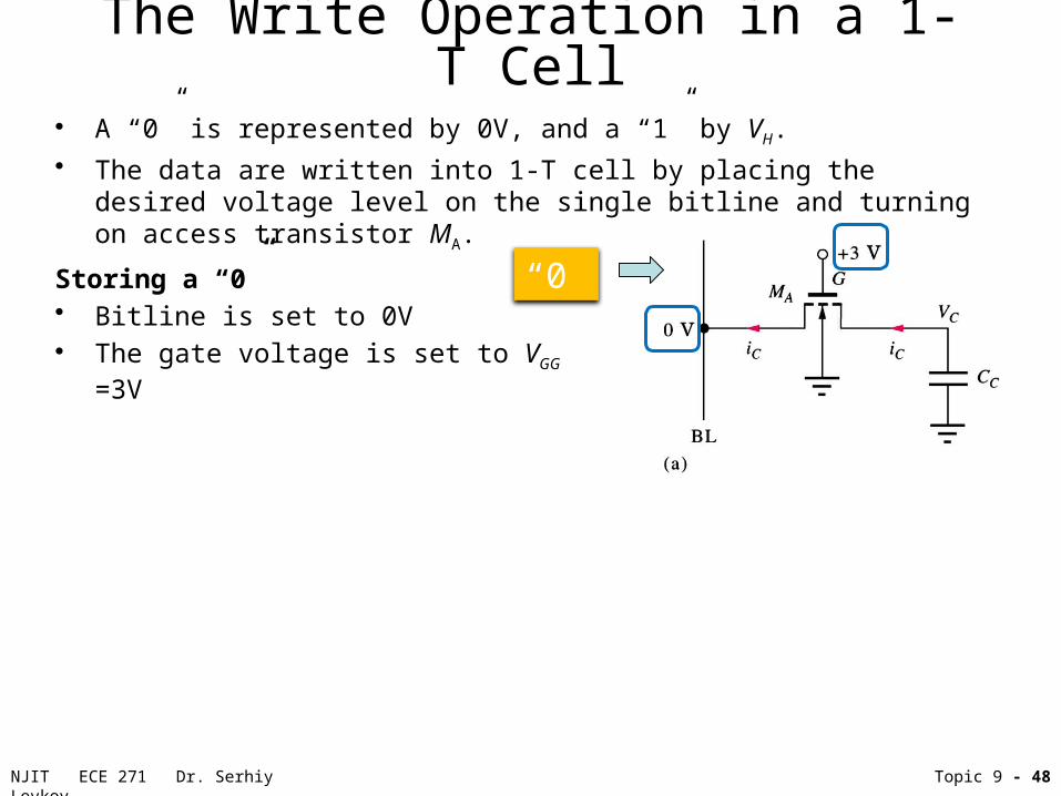
• A “0” is represented by 0V, and a “1” by VH.
• The data are written into 1-T cell by placing the desired voltage level on the single bitline and turning on access transistor MA.
Storing a “0”• Bitline is set to 0V• The gate voltage is set to VGG =3V
“0”
The Write Operation in a 1-T Cell
NJIT ECE 271 Dr. Serhiy Levkov Topic 9 - 49
• A “0” is represented by 0V, and a “1” by VH.
• The data are written into 1-T cell by placing the desired voltage level on the single bitline and turning on access transistor MA.
Storing a “0”• Bitline is set to 0V• The gate voltage is set to VGG =3V
• The bitline terminal of the MA acts like a source.
“0”
The Write Operation in a 1-T Cell
NJIT ECE 271 Dr. Serhiy Levkov Topic 9 - 50
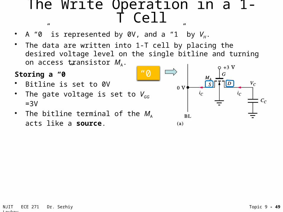
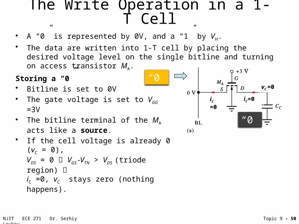
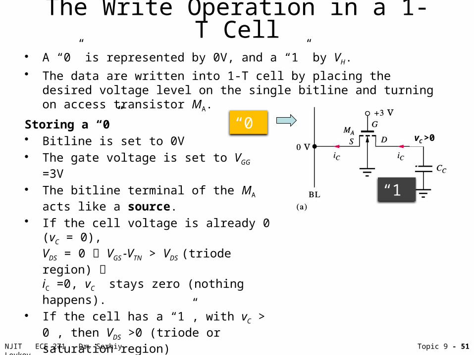
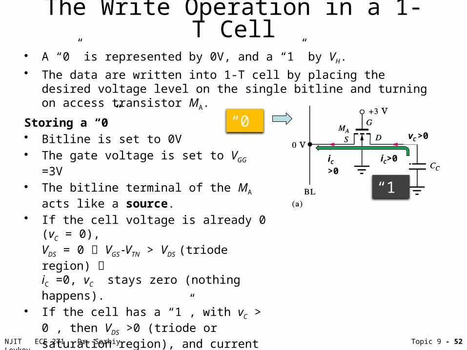
• A “0” is represented by 0V, and a “1” by VH.
• The data are written into 1-T cell by placing the desired voltage level on the single bitline and turning on access transistor MA.
Storing a “0”• Bitline is set to 0V• The gate voltage is set to VGG =3V
• The bitline terminal of the MA acts like a source.
• If the cell voltage is already 0 (vC = 0), VDS = 0 VGS -VTN > VDS (triode region) iC =0, vC stays zero (nothing happens).
“0”
“0”
iC =0 iC=0
vC =0
The Write Operation in a 1-T Cell
NJIT ECE 271 Dr. Serhiy Levkov Topic 9 - 51
• A “0” is represented by 0V, and a “1” by VH.
• The data are written into 1-T cell by placing the desired voltage level on the single bitline and turning on access transistor MA.
Storing a “0”• Bitline is set to 0V• The gate voltage is set to VGG =3V
• The bitline terminal of the MA acts like a source.
• If the cell voltage is already 0 (vC = 0), VDS = 0 VGS -VTN > VDS (triode region) iC =0, vC stays zero (nothing happens).
• If the cell has a “1”, with vC > 0 , then VDS >0 (triode or saturation region)
“0”
“1”
vC >0
The Write Operation in a 1-T Cell
NJIT ECE 271 Dr. Serhiy Levkov Topic 9 - 52
• A “0” is represented by 0V, and a “1” by VH.
• The data are written into 1-T cell by placing the desired voltage level on the single bitline and turning on access transistor MA.
Storing a “0”• Bitline is set to 0V• The gate voltage is set to VGG =3V
• The bitline terminal of the MA acts like a source.
• If the cell voltage is already 0 (vC = 0), VDS = 0 VGS -VTN > VDS (triode region) iC =0, vC stays zero (nothing happens).
• If the cell has a “1”, with vC > 0 , then VDS >0 (triode or saturation region), and current iC > 0
“0”
“1”
vC >0
iC >0 iC>0
The Write Operation in a 1-T Cell
NJIT ECE 271 Dr. Serhiy Levkov Topic 9 - 53
• A “0” is represented by 0V, and a “1” by VH.
• The data are written into 1-T cell by placing the desired voltage level on the single bitline and turning on access transistor MA.
Storing a “0”• Bitline is set to 0V• The gate voltage is set to VDD =3V
• The bitline terminal of the MA acts like a source.
• If the cell voltage is already 0 (vC = 0), VDS = 0 VGS -VTN > VDS (triode region) iC =0, vC stays zero (nothing happens).
• If the cell has a “1”, with vC > 0 , then VDS >0 (triode or saturation region), and current iC > 0 will completely discharge CC yielding vC =0.
“0”
“0”
vC =0
iC =0 iC=0
The Write Operation in a 1-T Cell
NJIT ECE 271 Dr. Serhiy Levkov Topic 9 - 54
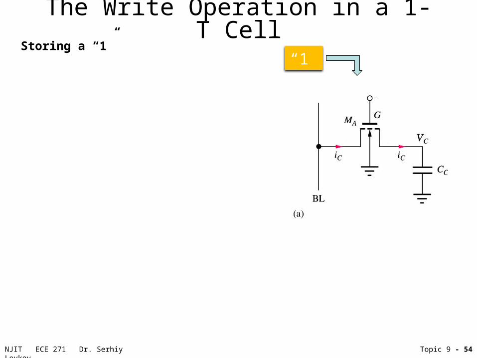
Storing a “1”“1”
The Write Operation in a 1-T Cell

NJIT ECE 271 Dr. Serhiy Levkov Topic 9 - 55
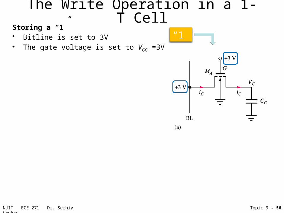
Storing a “1”• Bitline is set to 3V “1”
The Write Operation in a 1-T Cell
NJIT ECE 271 Dr. Serhiy Levkov Topic 9 - 56
Storing a “1”• Bitline is set to 3V• The gate voltage is set to VGG =3V
“1”
The Write Operation in a 1-T Cell

NJIT ECE 271 Dr. Serhiy Levkov Topic 9 - 57
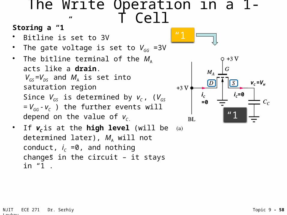
Storing a “1”• Bitline is set to 3V• The gate voltage is set to VGG =3V
• The bitline terminal of the MA acts like a drain. VGS =VDS and MA is set into saturation region
Since VGS is determined by vC , (VGS = VGG - vC ) the further events will depend on the value of vC .
“1”
The Write Operation in a 1-T Cell
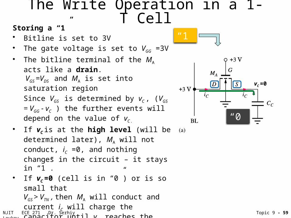
NJIT ECE 271 Dr. Serhiy Levkov Topic 9 - 58
“1”
vC =VH
iC =0 iC=0
Storing a “1”• Bitline is set to 3V• The gate voltage is set to VGG =3V
• The bitline terminal of the MA acts like a drain. VGS =VDS and MA is set into saturation region
Since VGS is determined by vC , (VGS = VGG - vC ) the further events will depend on the value of vC .
• If vC is at the high level (will be determined later), MA will not conduct, iC =0, and nothing changes in the circuit – it stays in “1”.
“1”
The Write Operation in a 1-T Cell
NJIT ECE 271 Dr. Serhiy Levkov Topic 9 - 59
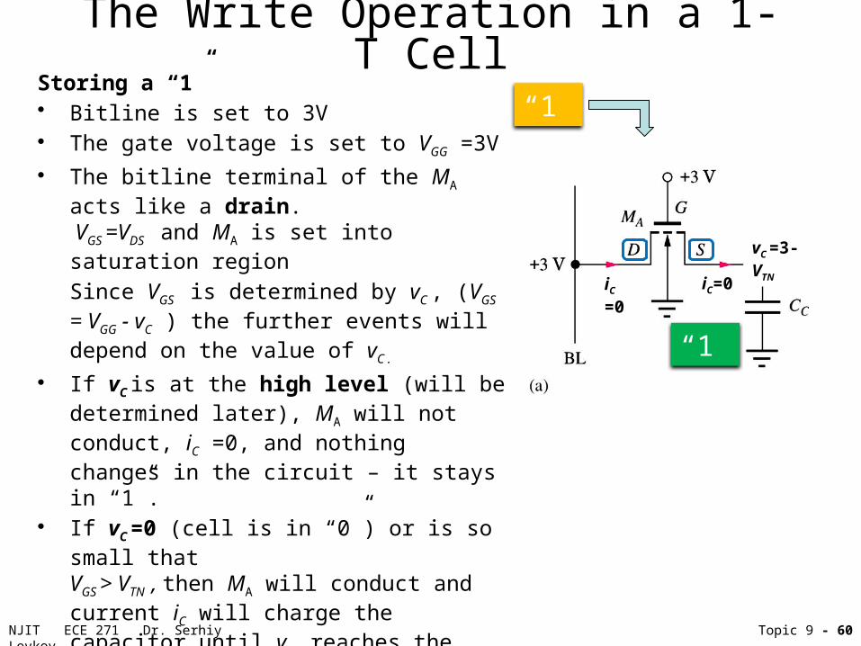
“0”
vC =0
Storing a “1”• Bitline is set to 3V• The gate voltage is set to VGG =3V
• The bitline terminal of the MA acts like a drain. VGS =VDS and MA is set into saturation region
Since VGS is determined by vC , (VGS = VGG - vC ) the further events will depend on the value of vC .
• If vC is at the high level (will be determined later), MA will not conduct, iC =0, and nothing changes in the circuit – it stays in “1”.
• If vC =0 (cell is in “0”) or is so small that VGS > VTN , then MA will conduct and current iC will charge the capacitor until vC reaches the value at which the current will stop.
“1”
The Write Operation in a 1-T Cell
NJIT ECE 271 Dr. Serhiy Levkov Topic 9 - 60
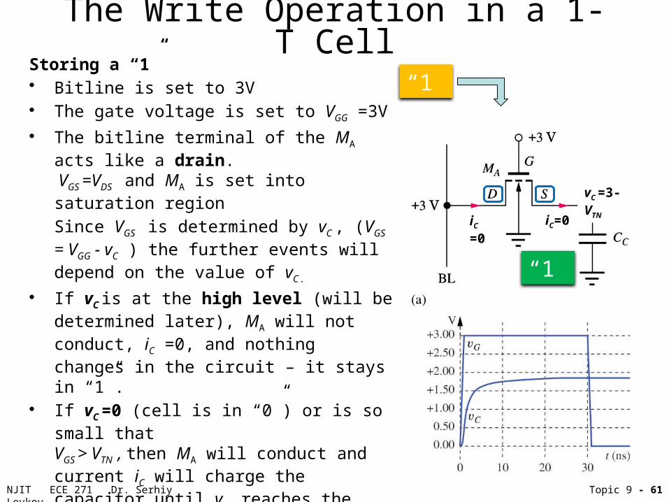
vC =3- VTN
iC =0 iC=0
“1”
Storing a “1”• Bitline is set to 3V• The gate voltage is set to VGG =3V
• The bitline terminal of the MA acts like a drain. VGS =VDS and MA is set into saturation region
Since VGS is determined by vC , (VGS = VGG - vC ) the further events will depend on the value of vC .
• If vC is at the high level (will be determined later), MA will not conduct, iC =0, and nothing changes in the circuit – it stays in “1”.
• If vC =0 (cell is in “0”) or is so small that VGS > VTN , then MA will conduct and current iC will charge the capacitor until vC reaches the value at which the current will stop.
• That will happen when VGS =VTN or vC = VGG -VTN
at which point the cell comes to “1” state thus vC = 3-VTN will correspond to the “1” .
“1”
The Write Operation in a 1-T Cell
NJIT ECE 271 Dr. Serhiy Levkov Topic 9 - 61
Storing a “1”• Bitline is set to 3V• The gate voltage is set to VGG =3V
• The bitline terminal of the MA acts like a drain. VGS =VDS and MA is set into saturation region
Since VGS is determined by vC , (VGS = VGG - vC ) the further events will depend on the value of vC .
• If vC is at the high level (will be determined later), MA will not conduct, iC =0, and nothing changes in the circuit – it stays in “1”.
• If vC =0 (cell is in “0”) or is so small that VGS > VTN , then MA will conduct and current iC will charge the capacitor until vC reaches the value at which the current will stop.
• That will happen when VGS =VTN or vC = VGG -VTN
at which point the cell comes to “1” state thus vC = 3-VTN will correspond to the “1” .
• Notice that the voltage stored on the storage capacitor does not reach VGG
“1”
vC =3- VTN
iC =0 iC=0
“1”
The Write Operation in a 1-T Cell

NJIT ECE 271 Dr. Serhiy Levkov Topic 9 - 62
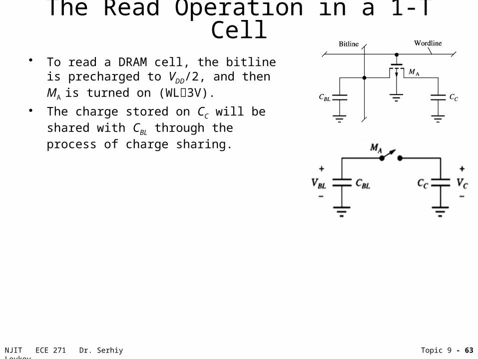
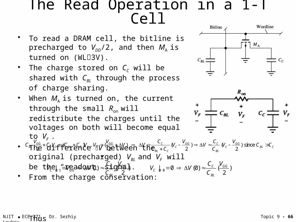
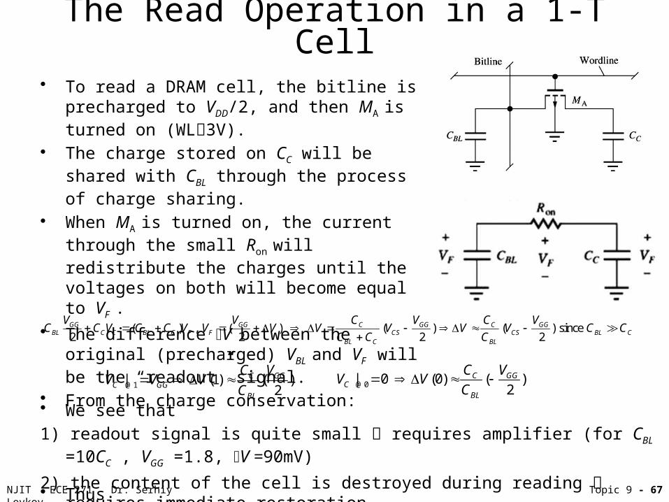
The Read Operation in a 1-T Cell
• To read a DRAM cell, the bitline is precharged to VDD/2, and then MA is turned on (WL3V).
NJIT ECE 271 Dr. Serhiy Levkov Topic 9 - 63
The Read Operation in a 1-T Cell
• To read a DRAM cell, the bitline is precharged to VDD/2, and then MA is turned on (WL3V).
• The charge stored on CC will be shared with CBL through the process of charge sharing.

NJIT ECE 271 Dr. Serhiy Levkov Topic 9 - 64
• To read a DRAM cell, the bitline is precharged to VDD/2, and then MA is turned on (WL3V).
• The charge stored on CC will be shared with CBL through the process of charge sharing.
• When MA is turned on, the current through the small Ron will redistribute the charges until the voltages on both will become equal to VF .
The Read Operation in a 1-T Cell
VBL VC

NJIT ECE 271 Dr. Serhiy Levkov Topic 9 - 65
• To read a DRAM cell, the bitline is precharged to VDD/2, and then MA is turned on (WL3V).
• The charge stored on CC will be shared with CBL through the process of charge sharing.
• When MA is turned on, the current through the small Ron will redistribute the charges until the voltages on both will become equal to VF .
• The difference between the original (precharged) VBL and VF will be the “readout” signal.
The Read Operation in a 1-T Cell
NJIT ECE 271 Dr. Serhiy Levkov Topic 9 - 66
• To read a DRAM cell, the bitline is precharged to VDD/2, and then MA is turned on (WL3V).
• The charge stored on CC will be shared with CBL through the process of charge sharing.
• When MA is turned on, the current through the small Ron will redistribute the charges until the voltages on both will become equal to VF .
• The difference DV between the original (precharged) VBL and VF will be the “readout” signal.
• From the charge conservation:
• Thus and
The Read Operation in a 1-T Cell
( ) , ( ) ( ) ( ) since2 2 2 2GG GG C GG C GG
BL C C BL C F F C C BL CBL C BL
V V C V C VC C V C C V V V V V V V C C
C C C
@1| (1) ( )2
C GGC GG
BL
C VV V V
C @ 0| 0 (0) ( )
2C GG
CBL
C VV V
C
NJIT ECE 271 Dr. Serhiy Levkov Topic 9 - 67
• To read a DRAM cell, the bitline is precharged to VDD/2, and then MA is turned on (WL3V).
• The charge stored on CC will be shared with CBL through the process of charge sharing.
• When MA is turned on, the current through the small Ron will redistribute the charges until the voltages on both will become equal to VF .
• The difference DV between the original (precharged) VBL and VF will be the “readout” signal.
• From the charge conservation:
• Thus and
The Read Operation in a 1-T Cell
( ) , ( ) ( ) ( ) since2 2 2 2GG GG C GG C GG
BL C C BL C F F CS CS BL CBL C BL
V V C V C VC C V C C V V V V V V V C C
C C C
@1| (1) ( )2
C GGC GG
BL
C VV V V
C @0| 0 (0) ( )
2C GG
CBL
C VV V
C
• We see that
1) readout signal is quite small requires amplifier (for CBL =10CC , VGG =1.8, DV =90mV)
2) the content of the cell is destroyed during reading requires immediate restoration

NJIT ECE 271 Dr. Serhiy Levkov Topic 9 - 68
Sense Amplifiers• Sense amplifiers are used to detect the small currents that flow through the access
transistors or the small voltage differences that occur during charge sharing.• One sense amplifier is associated with each bitline pair.

NJIT ECE 271 Dr. Serhiy Levkov Topic 9 - 69
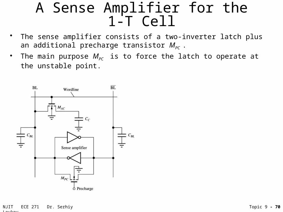
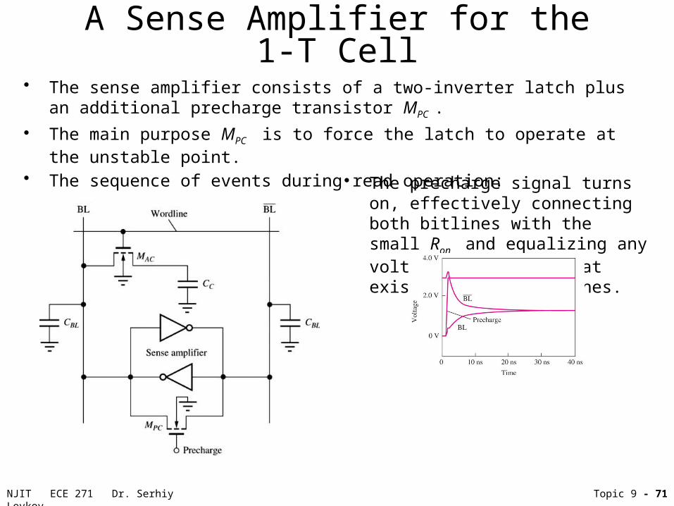
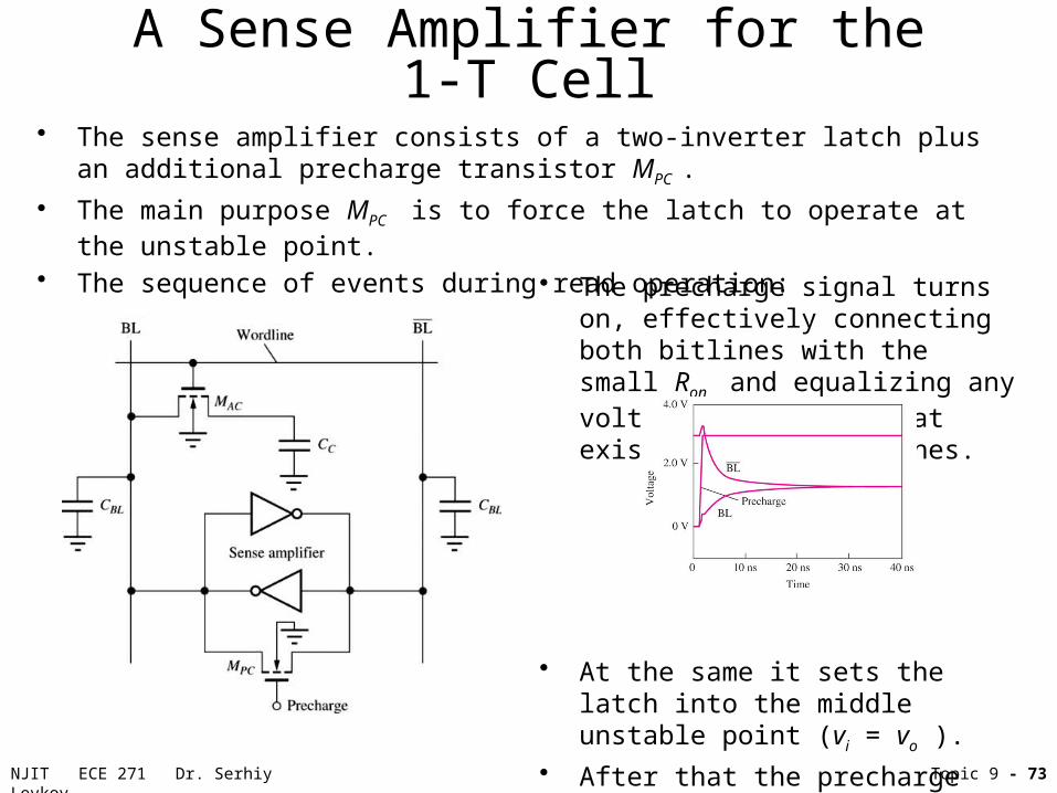
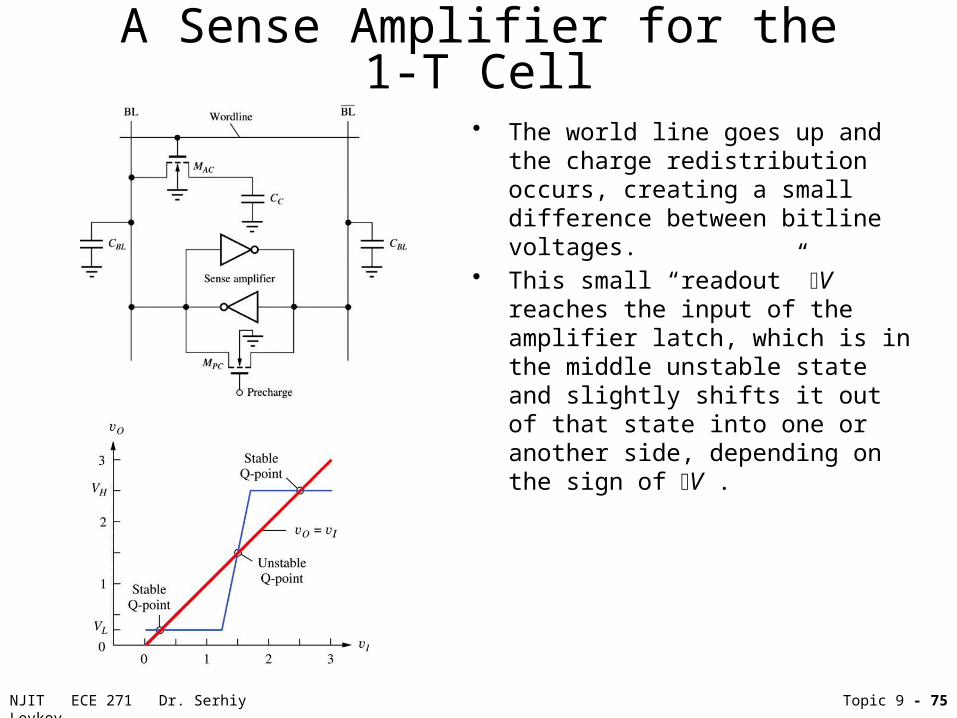
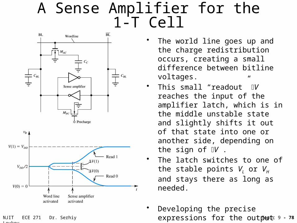
A Sense Amplifier for the 1-T Cell• The sense amplifier consists of a two-inverter latch plus an additional precharge
transistor MPC .
NJIT ECE 271 Dr. Serhiy Levkov Topic 9 - 70
A Sense Amplifier for the 1-T Cell• The sense amplifier consists of a two-inverter latch plus an additional precharge
transistor MPC .
• The main purpose MPC is to force the latch to operate at the unstable point.
NJIT ECE 271 Dr. Serhiy Levkov Topic 9 - 71
A Sense Amplifier for the 1-T Cell
• The precharge signal turns on, effectively connecting both bitlines with the small Ron and equalizing any voltage difference that existed between bitlines.
• The sense amplifier consists of a two-inverter latch plus an additional precharge transistor MPC .
• The main purpose MPC is to force the latch to operate at the unstable point.
• The sequence of events during read operation:

NJIT ECE 271 Dr. Serhiy Levkov Topic 9 - 72
A Sense Amplifier for the 1-T Cell
• The precharge signal turns on, effectively connecting both bitlines with the small Ron and equalizing any voltage difference that existed between bitlines.
• At the same time it sets the latch into the middle unstable point (vi = vo ).
• The sense amplifier consists of a two-inverter latch plus an additional precharge transistor MPC .
• The main purpose MPC is to force the latch to operate at the unstable point.
• The sequence of events during read operation:
NJIT ECE 271 Dr. Serhiy Levkov Topic 9 - 73
A Sense Amplifier for the 1-T Cell
• The precharge signal turns on, effectively connecting both bitlines with the small Ron and equalizing any voltage difference that existed between bitlines.
• At the same it sets the latch into the middle unstable point (vi = vo ).
• After that the precharge signal may go off and the latch will remain in the unstable equilibrium.
• The sense amplifier consists of a two-inverter latch plus an additional precharge transistor MPC .
• The main purpose MPC is to force the latch to operate at the unstable point.
• The sequence of events during read operation:

NJIT ECE 271 Dr. Serhiy Levkov Topic 9 - 74
A Sense Amplifier for the 1-T Cell
• The world line goes up and the charge redistribution occurs, creating a small difference between bitline voltages.
NJIT ECE 271 Dr. Serhiy Levkov Topic 9 - 75
A Sense Amplifier for the 1-T Cell
• The world line goes up and the charge redistribution occurs, creating a small difference between bitline voltages.
• This small “readout” DV reaches the input of the amplifier latch, which is in the middle unstable state and slightly shifts it out of that state into one or another side, depending on the sign of DV .

NJIT ECE 271 Dr. Serhiy Levkov Topic 9 - 76
A Sense Amplifier for the 1-T Cell
• The world line goes up and the charge redistribution occurs, creating a small difference between bitline voltages.
• This small “readout” DV reaches the input of the amplifier latch, which is in the middle unstable state and slightly shifts it out of that state into one or another side, depending on the sign of DV .
• The latch switches to one of the stable points VL or VH and stays there as long as needed.

NJIT ECE 271 Dr. Serhiy Levkov Topic 9 - 77
A Sense Amplifier for the 1-T Cell
• The world line goes up and the charge redistribution occurs, creating a small difference between bitline voltages.
• This small “readout” DV reaches the input of the amplifier latch, which is in the middle unstable state and slightly shifts it out of that state into one or another side, depending on the sign of DV
• The latch switches to one of the stable points VL or VH and stays there as long as needed.
NJIT ECE 271 Dr. Serhiy Levkov Topic 9 - 78
A Sense Amplifier for the 1-T Cell
• The world line goes up and the charge redistribution occurs, creating a small difference between bitline voltages.
• This small “readout” DV reaches the input of the amplifier latch, which is in the middle unstable state and slightly shifts it out of that state into one or another side, depending on the sign of DV .
• The latch switches to one of the stable points VL or VH and stays there as long as needed.
• Developing the precise expressions for the output of the sense amplifier is a difficult task because the large signal models have to be used and the positive feedback should be taken into the account.
NJIT ECE 271 Dr. Serhiy Levkov Topic 9 - 79
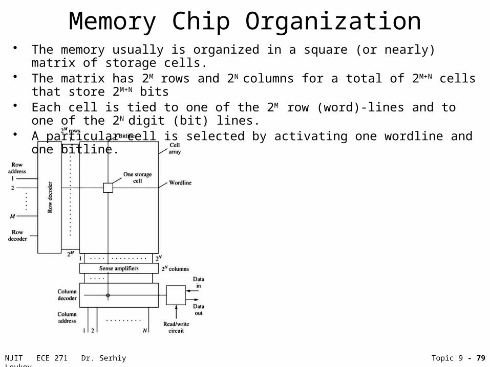
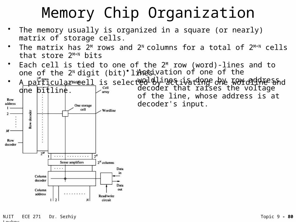
Memory Chip Organization• The memory usually is organized in a square (or nearly) matrix of storage cells.• The matrix has 2M rows and 2N columns for a total of 2M+N cells that store 2M+N bits• Each cell is tied to one of the 2M row (word)-lines and to one of the 2N digit (bit) lines. • A particular cell is selected by activating one wordline and one bitline.
NJIT ECE 271 Dr. Serhiy Levkov Topic 9 - 80
Memory Chip Organization
• Activation of one of the woldlines is done by row address decoder that raises the voltage of the line, whose address is at decoder's input.
• The memory usually is organized in a square (or nearly) matrix of storage cells.• The matrix has 2M rows and 2N columns for a total of 2M+N cells that store 2M+N bits• Each cell is tied to one of the 2M row (word)-lines and to one of the 2N digit (bit) lines. • A particular cell is selected by activating one wordline and one bitline.

NJIT ECE 271 Dr. Serhiy Levkov Topic 9 - 81
Memory Chip Organization
• Activation of one of the woldlines is done by row address decoder that raises the voltage of the line, whose address is at decoder's input.
• When Kth row (word) is selected, all 2N cells provide their content to the respective bit lines and their voltage will be changed by a small amount.
• The memory usually is organized in a square (or nearly) matrix of storage cells.• The matrix has 2M rows and 2N columns for a total of 2M+N cells that store 2M+N bits• Each cell is tied to one of the 2M row (word)-lines and to one of the 2N digit (bit) lines. • A particular cell is selected by activating one wordline and one bitline.

NJIT ECE 271 Dr. Serhiy Levkov Topic 9 - 82
Memory Chip Organization
• Activation of one of the woldlines is done by row address decoder that raises the voltage of the line, whose address is at decoder's input.
• When Kth row (word) is selected, all 2N cells provide their content to the respective bit lines and their voltage will be changed by a small amount.
• It will be amplified in the sense amplifier and the normal digital word (combination of bits) will enter into the column decoder.
•
• The memory usually is organized in a square (or nearly) matrix of storage cells.• The matrix has 2M rows and 2N columns for a total of 2M+N cells that store 2M+N bits• Each cell is tied to one of the 2M row (word)-lines and to one of the 2N digit (bit) lines. • A particular cell is selected by activating one wordline and one bitline.

NJIT ECE 271 Dr. Serhiy Levkov Topic 9 - 83
Memory Chip Organization
• Activation of one of the woldlines is done by row address decoder that raises the voltage of the line, whose address is at decoder's input.
• When Kth row (word) is selected, all 2N cells provide their content to the respective bit lines and their voltage will be changed by a small amount.
• It will be amplified in the sense amplifier and the normal digital word (combination of bits) will enter into the column decoder.
• The column decoder selects a signal of a column whose Nbit address is applied to the decoder’s input.
• That signal will appear on the data out line.
• The memory usually is organized in a square (or nearly) matrix of storage cells.• The matrix has 2M rows and 2N columns for a total of 2M+N cells that store 2M+N bits• Each cell is tied to one of the 2M row (word)-lines and to one of the 2N digit (bit) lines. • A particular cell is selected by activating one wordline and one bitline.

NJIT ECE 271 Dr. Serhiy Levkov Topic 9 - 84
Memory Chip Organization
• Activation of one of the woldlines is done by row address decoder that raises the voltage of the line, whose address is at decoder's input.
• When Kth row (word) is selected, all 2N cells provide their content to the respective bit lines and their voltage will be changed by a small amount.
• It will be amplified in the sense amplifier and the normal digital word (combination of bits) will enter into the column decoder.
• The column decoder selects a signal of a column whose Nbit address is applied to the decoder’s input.
• That signal will appear on the data out line.• The matrix organization allows to shorten the
length of address the length of bit/word lines their resistance and capacitance increase the speed of memory work.
• The memory usually is organized in a square (or nearly) matrix of storage cells.• The matrix has 2M rows and 2N columns for a total of 2M+N cells that store 2M+N bits• Each cell is tied to one of the 2M row (word)-lines and to one of the 2N digit (bit) lines. • A particular cell is selected by activating one wordline and one bitline.
NJIT ECE 271 Dr. Serhiy Levkov Topic 9 - 85
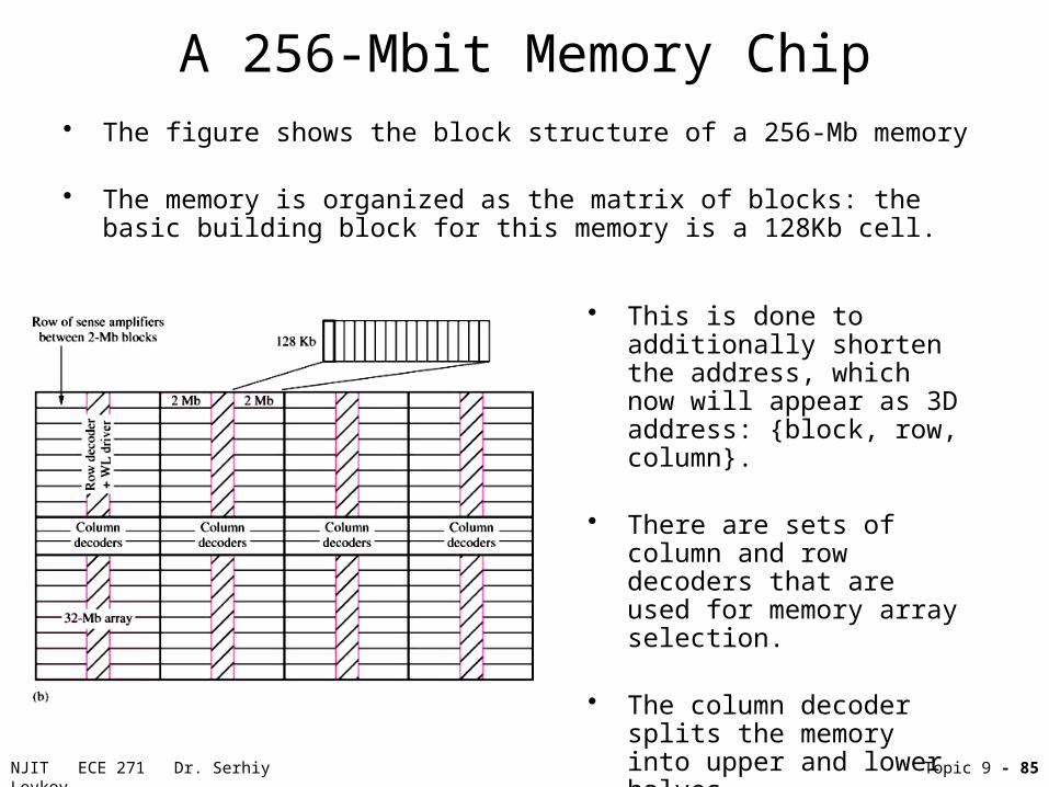
A 256-Mbit Memory Chip
• This is done to additionally shorten the address, which now will appear as 3D address: {block, row, column}.
• There are sets of column and row decoders that are used for memory array selection.
• The column decoder splits the memory into upper and lower halves.
• The figure shows the block structure of a 256-Mb memory
• The memory is organized as the matrix of blocks: the basic building block for this memory is a 128Kb cell.
NJIT ECE 271 Dr. Serhiy Levkov Topic 9 - 86
Address Decoders• Two major types of decoders are used.• NMOS row and column address decoders to select a single row/column• NMOS pass transistor tree decoders for selecting groups of data bits.
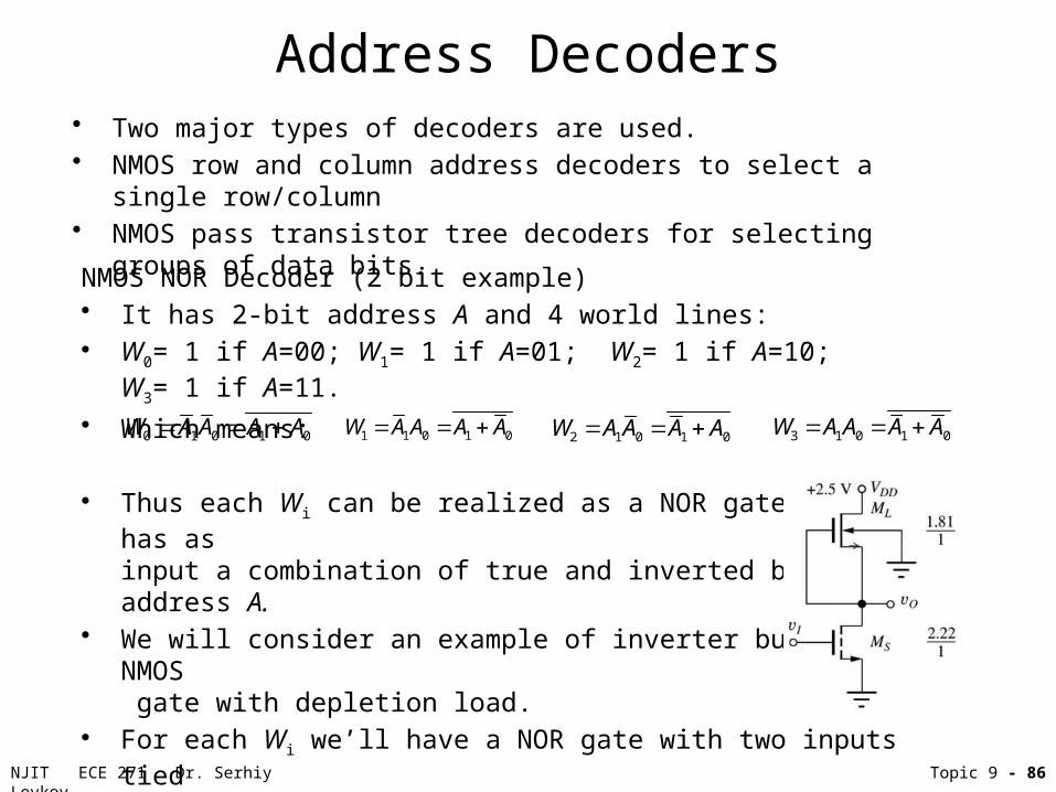
NMOS NOR Decoder (2 bit example)• It has 2-bit address A and 4 world lines:• W0= 1 if A=00; W1= 1 if A=01; W2= 1 if A=10; W3= 1 if A=11.
• Which means:
• Thus each Wi can be realized as a NOR gate that has as input a combination of true and inverted bits of address A.
• We will consider an example of inverter built on NMOS gate with depletion load.
• For each Wi we’ll have a NOR gate with two inputs tied to appropriate true and inverted bits of A.
0 1 0 1 0W A A A A 1 1 0 1 0W A A A A 2 1 0 1 0W A A A A 3 1 0 1 0W A A A A

NJIT ECE 271 Dr. Serhiy Levkov Topic 9 - 87
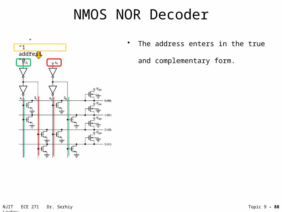
NMOS NOR Decoder
• The address enters in the true “1” address “0”
NJIT ECE 271 Dr. Serhiy Levkov Topic 9 - 88
NMOS NOR Decoder
• The address enters in the true and complementary form.
“1” address “0”
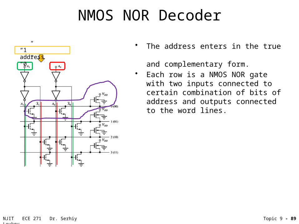
NJIT ECE 271 Dr. Serhiy Levkov Topic 9 - 89
NMOS NOR Decoder
• The address enters in the true and complementary form.
• Each row is a NMOS NOR gate with two inputs connected to certain combination of bits of address and outputs connected to the word lines.
“1” address “0”

NJIT ECE 271 Dr. Serhiy Levkov Topic 9 - 90
NMOS NOR Decoder
• The address enters in the true and complementary form.
• Each row is a NMOS NOR gate with two inputs connected to certain combination of bits of address and outputs connected to the word lines.
• The output of each NOR gate is low when any of the inputs are high ( at least one transistor is on).
“1” address “0”
NJIT ECE 271 Dr. Serhiy Levkov Topic 9 - 91
NMOS NOR Decoder
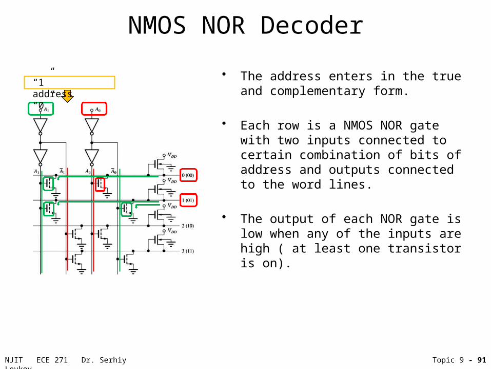
• The address enters in the true and complementary form.
• Each row is a NMOS NOR gate with two inputs connected to certain combination of bits of address and outputs connected to the word lines.
• The output of each NOR gate is low when any of the inputs are high ( at least one transistor is on).
“1” address “0”

NJIT ECE 271 Dr. Serhiy Levkov Topic 9 - 92
NMOS NOR Decoder
• The address enters in the true and complementary form.
• Each row is a NMOS NOR gate with two inputs connected to certain combination of bits of address and outputs connected to the word lines.
• The output of each NOR gate is low when any of the inputs are high ( at least one transistor is on).
“1” address “0”
NJIT ECE 271 Dr. Serhiy Levkov Topic 9 - 93
NMOS NOR Decoder
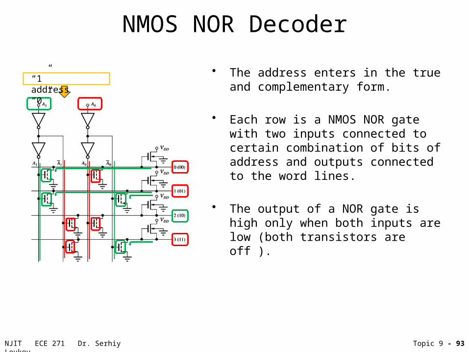
• The address enters in the true and complementary form.
• Each row is a NMOS NOR gate with two inputs connected to certain combination of bits of address and outputs connected to the word lines.
• The output of a NOR gate is high only when both inputs are low (both transistors are off ).
“1” address “0”

NJIT ECE 271 Dr. Serhiy Levkov Topic 9 - 94
NMOS NOR Decoder
• The address enters in the true and complementary form.
• Each row is a NMOS NOR gate with two inputs connected to certain combination of bits of address and outputs connected to the word lines.
• The output of a NOR gate is high only when both inputs are low (both transistors are off ).
• For every input, only one output line will be high – the rest will be always low.
“1” address “0”

NJIT ECE 271 Dr. Serhiy Levkov Topic 9 - 95
NMOS NAND Decoder
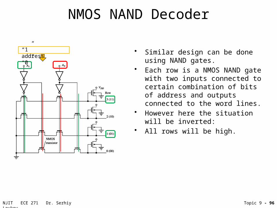
• Similar design can be done using NAND gates.
• Each row is a NMOS NAND gate with two inputs connected to certain combination of bits of address and outputs connected to the word lines.
• However here the situation will be inverted: • All rows will be high.
“1” address “0”
NJIT ECE 271 Dr. Serhiy Levkov Topic 9 - 96
NMOS NAND Decoder
• Similar design can be done using NAND gates.
• Each row is a NMOS NAND gate with two inputs connected to certain combination of bits of address and outputs connected to the word lines.
• However here the situation will be inverted: • All rows will be high.
“1” address “0”
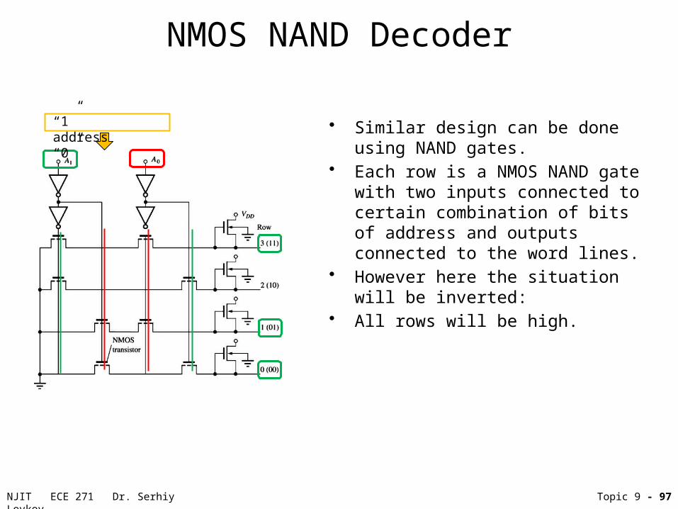
NJIT ECE 271 Dr. Serhiy Levkov Topic 9 - 97
NMOS NAND Decoder
• Similar design can be done using NAND gates.
• Each row is a NMOS NAND gate with two inputs connected to certain combination of bits of address and outputs connected to the word lines.
• However here the situation will be inverted: • All rows will be high.
“1” address “0”

NJIT ECE 271 Dr. Serhiy Levkov Topic 9 - 98
NMOS NAND Decoder
• Similar design can be done using NAND gates.
• Each row is a NMOS NAND gate with two inputs connected to certain combination of bits of address and outputs connected to the word lines.
• However here the situation will be inverted: • All rows will be high.• And only one row will be low that
correspond to the given address.• Thus we would need to invert the signal
coming to the wordlines, which is not a problem since anyway , additional driver circuits are required between the decoder and highly capacitive wordlines.
“1” address “0”
Related Documents