Design challenges of the 90nm technology node: responses by the FLOMERICS Group New Techniques for Chip and Package Thermal Modeling New Techniques for Chip and Package Thermal Modeling 3rd Annual "The Heat is On" Thermal Management in Microelectronics: Challenges and Innovations February 2007 Meptec

Welcome message from author
This document is posted to help you gain knowledge. Please leave a comment to let me know what you think about it! Share it to your friends and learn new things together.
Transcript

Design challenges of the 90nm technology node: responses by the FLOMERICS Group
New Techniques for Chip and Package Thermal Modeling
New Techniques for Chip and Package Thermal Modeling
3rd Annual "The Heat is On"Thermal Management in Microelectronics:Challenges and InnovationsFebruary 2007Meptec
Meptec 2007: New Techniques for Chip and Package Thermal Modeling, Flomerics Inc and Gradient Design Automation
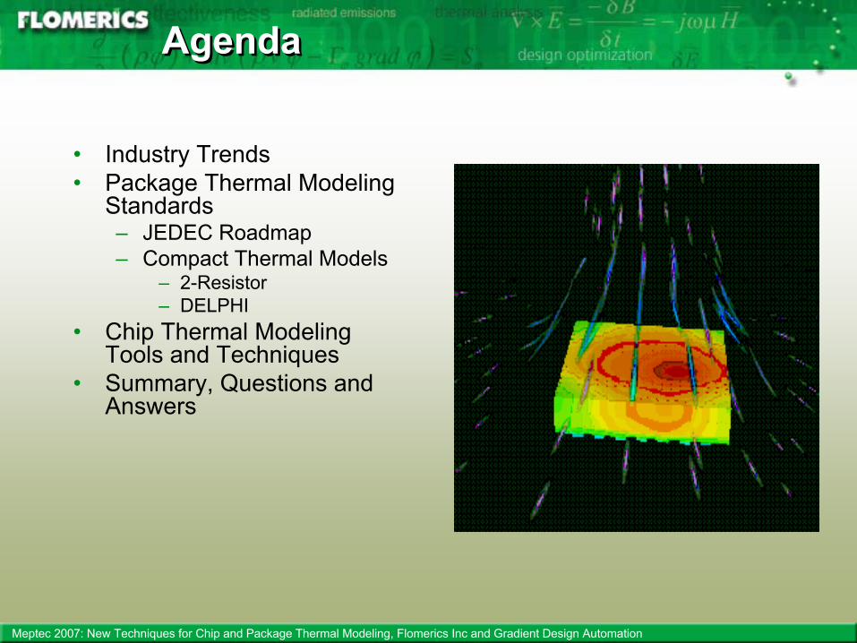
AgendaAgenda
• Industry Trends• Package Thermal Modeling
Standards– JEDEC Roadmap– Compact Thermal Models
– 2-Resistor– DELPHI
• Chip Thermal Modeling Tools and Techniques
• Summary, Questions and Answers

Meptec 2007: New Techniques for Chip and Package Thermal Modeling, Flomerics Inc and Gradient Design Automation
Industry DriversIndustry Drivers
• Moore’s Law– In 1965, Gordon Moore observed an
exponential growth in the number of transistors per integrated circuit and predicted that this trend would continue

Meptec 2007: New Techniques for Chip and Package Thermal Modeling, Flomerics Inc and Gradient Design Automation
Industry DriversIndustry Drivers
• Combined effect is an increase in (max) chip power…

Meptec 2007: New Techniques for Chip and Package Thermal Modeling, Flomerics Inc and Gradient Design Automation
Trends in Thermal DesignTrends in Thermal Design
Thermal solution innovation is moving downscale
System
Thermal design moves downscale as chip power increasesCo-design between levels and design data exchange are criticalNew standards and tools are needed to improve co-design, data exchange and detailed chip-package thermal analysis
PCB Package Chip
Mechanical Electromechanical Electrical

Meptec 2007: New Techniques for Chip and Package Thermal Modeling, Flomerics Inc and Gradient Design Automation
Co-Design and Data Exchange StandardsCo-Design and Data Exchange Standards
System PCB Package Chip
?
CTM standards for in-application junction temperature prediction
• FLOTHERM • Icepak• Coolit
• FLO/PCB• Iceboard• TASPCB• BetaSoft
• Flopack• Icechip• PTD
Proprietary exchange formats
Proprietary exchange formats
Meptec 2007: New Techniques for Chip and Package Thermal Modeling, Flomerics Inc and Gradient Design Automation
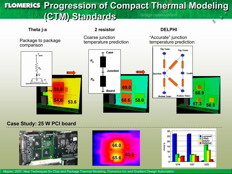
68.6
69.0
58.054.6
55.0
53.6 67.3
68.9
56.5
Progression of Compact Thermal Modeling (CTM) StandardsProgression of Compact Thermal Modeling (CTM) Standards
Theta j-a 2 resistor DELPHI
Package to package comparison
Coarse junction temperature prediction
“Accurate” junction temperature prediction
Case Study: 25 W PCI board
65.6
66.0
53.30
5
10
15
20
25
30
% Error
U16 U27 U25
Lumped2-ResDelphiDetailed
Meptec 2007: New Techniques for Chip and Package Thermal Modeling, Flomerics Inc and Gradient Design Automation
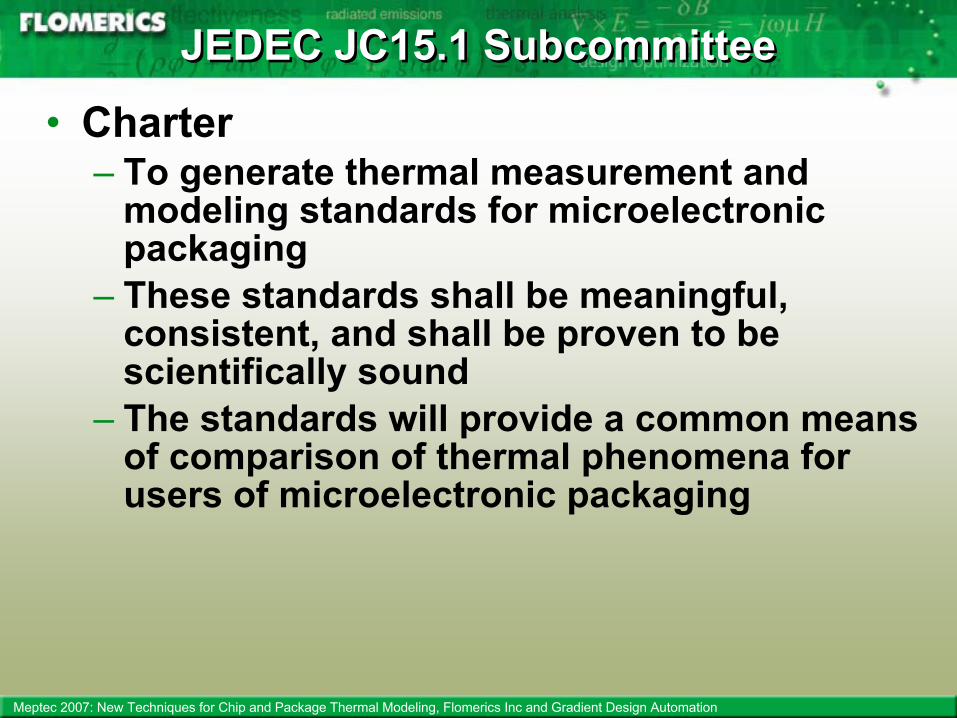
JEDEC JC15.1 Subcommittee JEDEC JC15.1 Subcommittee
• Charter– To generate thermal measurement and
modeling standards for microelectronic packaging
– These standards shall be meaningful, consistent, and shall be proven to be scientifically sound
– The standards will provide a common means of comparison of thermal phenomena for users of microelectronic packaging

Meptec 2007: New Techniques for Chip and Package Thermal Modeling, Flomerics Inc and Gradient Design Automation
All standards are available for downloading free of charge from www.jedec.org
Electrical TestMethod
JESD 51_1
Infrared TestMethod
Test MethodImplementationfor Active Die
Transient TestMethod
THERMALMEASUREMENT
NaturalConvectionJESD 51_2
ForcedConvectionJESD51-6
Heat SinkJunction-To-
Case
PCBJunction-To-
Board
THERMALENVIRONMENT
Low EffectiveThermal Cond.
Thermal Test Bd.JESD51_3
Hi EffectiveThermal Cond.
Thermal Test Bd.JESD51-7
Area ArrayThermal Test Bd.
Direct AttachThermal Test Bd.
JESD 51-5
Through HoleThermal Test Bd.
Array and DIL
Chip Size Package
Direct Chip AttachThermal Test Bd.
COMPONENTMOUNTING
Thermal Test ChipGuideline
(Wire Bond)JESD51_4
Thermal Test ChipGuideline
Flip-Chip / DCA
DEVICECONSTRUCTION
Detailed Model
Guideline
Submerged DualJet Impingement
Conduction ModelValidation Method
Dual Cold PlateConduction ModelValidation Method
Compact ModelGuideline
THERMALMODELING
Application ofThermal
Standards Guideline
SpecificationGuidelines for
PackageManufacturers
SpecificationGuidelines forPCB Tolerance
Verification
MEASUREMENTAPPLICATION
OVERVIEWJESD 51
Standard Published
Standard Proposed(in committee work group)
Standard Suggested
ThermocoupleMeasurement
Guideline
InterfaceMeasurement
Method
JESD51-8
JESD51-9
JESD 51-10 & 11
Published, Proposed, and Suggested StandardsPublished, Proposed, and Suggested Standards
Meptec 2007: New Techniques for Chip and Package Thermal Modeling, Flomerics Inc and Gradient Design Automation
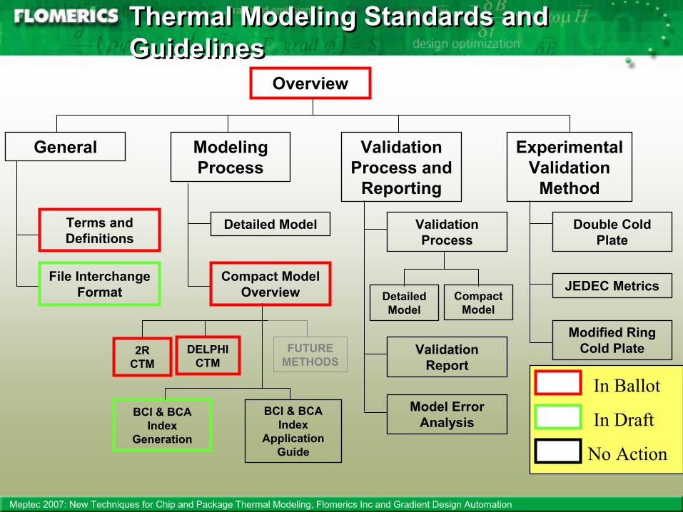
Thermal Modeling Standards and GuidelinesThermal Modeling Standards and Guidelines
Overview
General Modeling Process
Validation Process and
Reporting
Experimental Validation
Method
Terms and Definitions
File Interchange Format
Detailed Model
Compact Model Overview
Validation Process
Compact Model
2R CTM
Detailed Model
DELPHI CTM
FUTURE METHODS
Validation Report
Model Error Analysis
Double Cold Plate
JEDEC Metrics
Modified Ring Cold Plate
BCI & BCA Index
Application Guide
BCI & BCA Index
Generation
In Ballot
In Draft
No Action
Meptec 2007: New Techniques for Chip and Package Thermal Modeling, Flomerics Inc and Gradient Design Automation
Goals for Thermal Modeling StandardizationGoals for Thermal Modeling Standardization
• Generate standards governing thermal model generation, documentation, data exchange, and validation
• Promote more efficient division of labor between component suppliers and system integrators
• Complement test-based standards• Multi-parameter• Boundary condition independence (i.e. satisfy appropriate level
of Boundary Condition Independence or BCI) with numerically efficient predictive capabilities
• Capable of insertion into standard computational codes for system-level analysis
• Fully documented and non-proprietary

Meptec 2007: New Techniques for Chip and Package Thermal Modeling, Flomerics Inc and Gradient Design Automation
CTM SummaryCTM Summary• Chip level thermal design margins shrink with
miniaturization and increasing performance• New package modeling standards are needed
– To bridge the gap between semiconductor and systems manufacturers and minimize the cost of data exchange
– For reliable, accurate, in-application junction temperature prediction
– To control proprietary information• But what about the chip…?

New Techniques for Chip and Package Thermal Modeling
Dr. Edmund Cheng, PresidentGradient Design Automation
Santa Clara, Californiawww.gradient-da.com
MEPTEC, 3rd Annual “The Heat is On”, February 2007 Thermal Management in Microelectronics: Challenges and Innovations
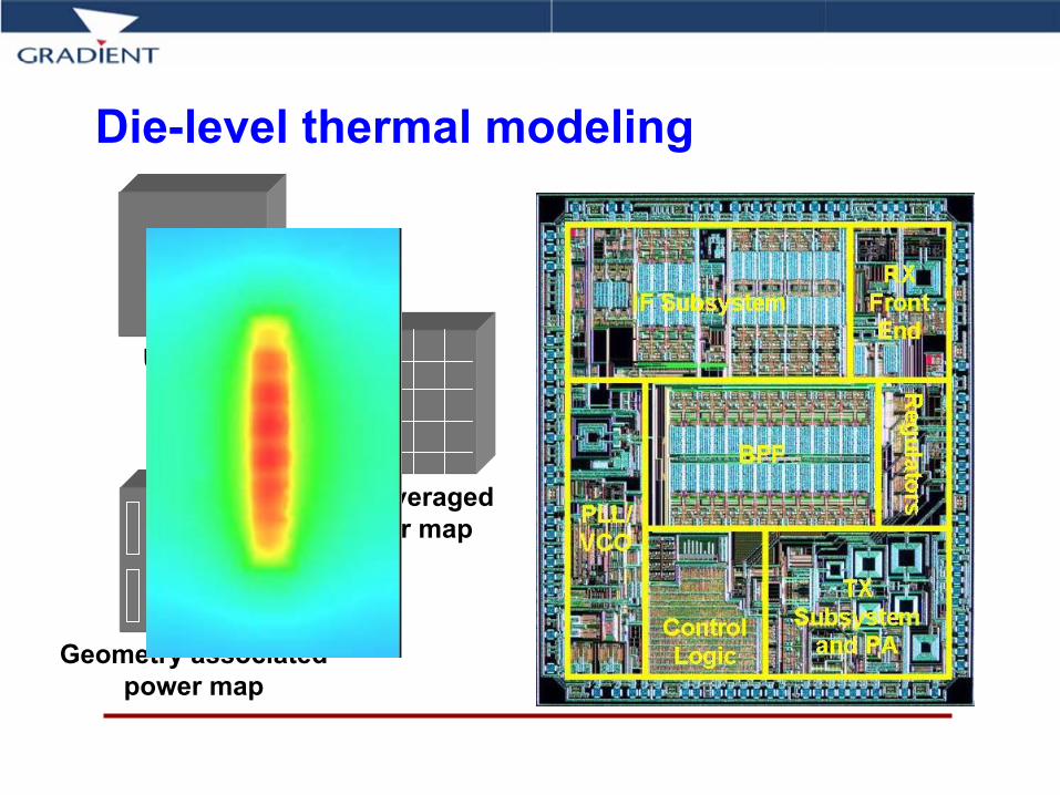
Die-level thermal modeling
Uniformpower
Geometry associatedpower map
Area averagedpower map
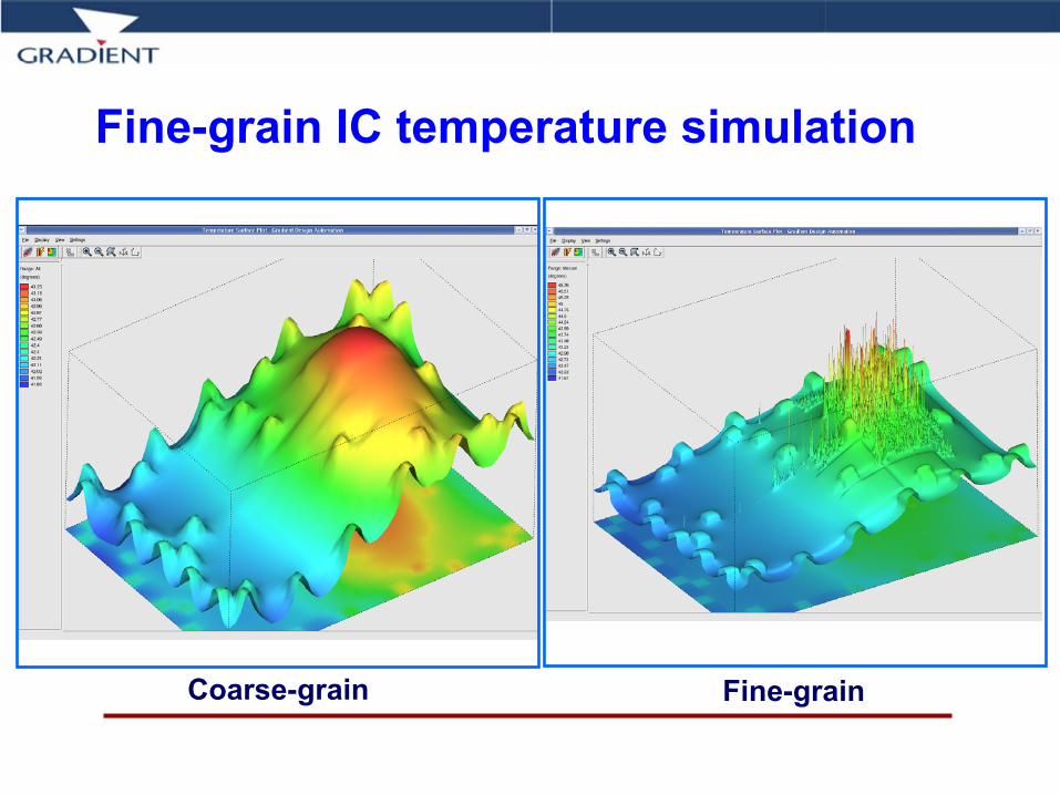
Fine-grain IC temperature simulation
Coarse-grain Fine-grain

Die-level thermal modeling
Designlayout
Powermodeling
Packagemodeling
Thermaltechfile
Thermal modeling
Reliabilitymodeling
Functionalitymodeling
Timingmodeling
Die stack-up

Data needed to run FireBolt
Chip layout is used to model the heat transport within the chip
e.g. LEF/DEF (or GDS2 if needed)Average power per circuit element from power analysis tools
e.g. Cadence Encounter Platform; Synopsys PrimeTime-PX
Package ΘJA (for each surface, or lumped)Thermal techfile – layer thicknesses (die stack-up) and material properties
De factostandard
EDA toolspecific
Gradientspecific
JEDECstandard
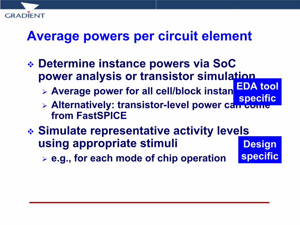
Average powers per circuit element
Determine instance powers via SoCpower analysis or transistor simulation
Average power for all cell/block instancesAlternatively: transistor-level power can come from FastSPICE
Simulate representative activity levels using appropriate stimuli
e.g., for each mode of chip operation
EDA toolspecific
Designspecific

Outputs from FireBolt
Steady-state 3-D temperature on the dieMetal wire temperatures are importantLow-K dielectrics: bad thermal conductors
Backannotates instance temperatures (per circuit element) to static TA and power analysis
Show the thermal impact on delay times, leakage currentse.g. Cadence Encounter Platform; Synopsys PrimeTime(-PX)
Gradientspecific
Gradientspecific

The temperature data can be used to:
Identify thermal hotspots, and verify that you are meeting the TJ-MAX specVerify that thermal gradients are harmlessHelp with thermal sensor placementMore accurately determine the thermal effects on critical aspects of the IC designs, such as leakage power, voltage drop and timing, signal crosstalk and timing, and electro-migration

Google Map for chip temperature?

Do you see where is the thermal problem?
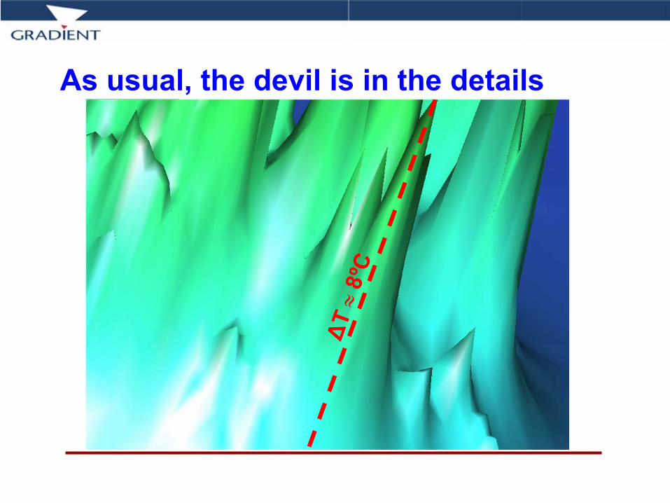
As usual, the devil is in the details
∆T ≈
8ºC

Package and IC co-simulationPackage model at horizontal face of die
Package-leveltemperature
Thermal profile at horizontal face of die
Die-leveltemperature
Meptec 2007: New Techniques for Chip and Package Thermal Modeling, Flomerics Inc and Gradient Design Automation
SummarySummary
• Miniaturization, performance and functionality trends are decreasing thermal design margins at the package the chip levels
• Modeling methodologies and standards must increase in sophistication to meet current and future chip and package design challenges. This is being realized by:– JEDEC CTM standards for packages– Emergence of fine-grain thermal analysis for
semiconductor chips– Emergence of multi-scale, chip-package-
environment analysis methodologies
Related Documents