Networks-on-Chip: Architectures, Design Methodologies, and Case Studies Guest Editors: Sao-Jie Chen, An-Yeu Andy Wu, and Jiang Xu Journal of Electrical and Computer Engineering

Welcome message from author
This document is posted to help you gain knowledge. Please leave a comment to let me know what you think about it! Share it to your friends and learn new things together.
Transcript
Networks-on-Chip: Architectures, Design Methodologies, and Case StudiesGuest Editors: Sao-Jie Chen, An-Yeu Andy Wu, and Jiang Xu
Journal of Electrical and Computer Engineering

Networks-on-Chip: Architectures,Design Methodologies, and Case Studies

Journal of Electrical and Computer Engineering
Networks-on-Chip: Architectures,Design Methodologies, and Case Studies
Guest Editors: Sao-Jie Chen, An-Yeu Andy Wu, and Jiang Xu

Copyright © 2011 Hindawi Publishing Corporation. All rights reserved.
This is a special issue published in volume 2011 of “Journal of Electrical and Computer Engineering.” All articles are open access articlesdistributed under the Creative Commons Attribution License, which permits unrestricted use, distribution, and reproduction in anymedium, provided the original work is properly cited.

Editorial BoardThe editorial board of the journal is organized into sections that correspond to
the subject areas covered by the journal.
Circuits and Systems
M. T. Abuelma’atti, Saudi ArabiaIshfaq Ahmad, USADhamin Al-Khalili, CanadaWael M. Badawy, CanadaIvo Barbi, BrazilMartin A. Brooke, USAChip Hong Chang, SingaporeY. W. Chang, TaiwanTian-Sheuan Chang, TaiwanTzi-Dar Chiueh, TaiwanHenry S. H. Chung, Hong KongM. Jamal Deen, CanadaAhmed El Wakil, UAEDenis Flandre, BelgiumP. Franzon, USAAndre Ivanov, CanadaEbroul Izquierdo, UKWen-Ben Jone, USA
Yong-Bin Kim, USAH. Kuntman, TurkeyParag K. Lala, USAShen-Iuan Liu, TaiwanBin-Da Liu, TaiwanJoao Antonio Martino, BrazilPianki Mazumder, USAMichel Nakhla, CanadaSing Kiong Nguang, New ZealandShun-ichiro Ohmi, JapanMohamed A. Osman, USAPing Feng Pai, TaiwanMarcelo Antonio Pavanello, BrazilMarco Platzner, GermanyMassimo Poncino, ItalyDhiraj K. Pradhan, UKF. Ren, USA
Gabriel Robins, USAMohamad Sawan, CanadaRaj Senani, IndiaGianluca Setti, ItalyJose Silva-Martinez, USAAhmed M. Soliman, EgyptDimitrios Soudris, GreeceCharles E. Stroud, USAEphraim Suhir, USAHannu Tenhunen, SwedenGeorge S. Tombras, GreeceSpyros Tragoudas, USAChi Kong Tse, Hong KongChi-Ying Tsui, Hong KongJan Van der Spiegel, USAChin-Long Wey, USA
Communications
Sofiene Affes, CanadaDharma Agrawal, USAH. Arslan, USAEdward Au, ChinaEnzo Baccarelli, ItalyStefano Basagni, USAJun Bi, ChinaZ. Chen, SingaporeRene Cumplido, MexicoLuca De Nardis, ItalyM.-G. Di Benedetto, ItalyJ. Fiorina, FranceLijia Ge, ChinaZabih F. Ghassemlooy, UK
K. Giridhar, IndiaAmoakoh Gyasi-Agyei, GhanaYaohui Jin, ChinaMandeep Jit Singh, MalaysiaPeter Jung, GermanyAdnan Kavak, TurkeyRajesh Khanna, IndiaKiseon Kim, Republic of KoreaD. I. Laurenson, UKTho Le-Ngoc, CanadaC. Leung, CanadaPetri Mahonen, GermanyM. Abdul Matin, BangladeshM. Najar, Spain
Mohammad S. Obaidat, USAAdam Panagos, USASamuel Pierre, CanadaJohn N. Sahalos, GreeceChristian Schlegel, CanadaVinod Sharma, IndiaIickho Song, Republic of KoreaIoannis Tomkos, GreeceChien Cheng Tseng, TaiwanGeorge Tsoulos, GreeceLaura Vanzago, ItalyRoberto Verdone, ItalyGuosen Yue, USAJian-Kang Zhang, Canada
Signal Processing
S. S. Agaian, USAP. Agathoklis, CanadaJaakko Astola, FinlandTamal Bose, USAA. G. Constantinides, UK
Paul Dan Cristea, RomaniaPetar M. Djuric, USAIgor Djurovic, MontenegroKaren Egiazarian, FinlandW. S. Gan, Singapore
Zabih F. Ghassemlooy, UKLing Guan, CanadaMartin Haardt, GermanyPeter Handel, SwedenAndreas Jakobsson, Sweden

Jiri Jan, Czech RepublicS. Jensen, DenmarkChi Chung Ko, SingaporeM. A. Lagunas, SpainJ. Lam, Hong KongD. I. Laurenson, UKRiccardo Leonardi, ItalyMark Liao, TaiwanStephen Marshall, UKAntonio Napolitano, Italy
Sven Nordholm, AustraliaS. Panchanathan, USAPeriasamy K. Rajan, USACedric Richard, FranceWilliam Sandham, UKRavi Sankar, USADan Schonfeld, USALing Shao, UKJohn J. Shynk, USAAndreas Spanias, USA
Srdjan Stankovic, MontenegroYannis Stylianou, GreeceIoan Tabus, FinlandJarmo Henrik Takala, FinlandA. H. Tewfik, USAJitendra Kumar Tugnait, USAVesa Valimaki, FinlandLuc Vandendorpe, BelgiumAri J. Visa, FinlandJar Ferr Yang, Taiwan

Contents
Networks-on-Chip: Architectures, Design Methodologies, and Case Studies, Sao-Jie Chen,An-Yeu Andy Wu, and Jiang XuVolume 2012, Article ID 634930, 1 page
Intelligent On/Off Dynamic Link Management for On-Chip Networks, Andreas G. Savva,Theocharis Theocharides, and Vassos SoteriouVolume 2012, Article ID 107821, 12 pages
A Buffer-Sizing Algorithm for Network-on-Chips with Multiple Voltage-Frequency Islands,Anish S. Kumar, M. Pawan Kumar, Srinivasan Murali, V. Kamakoti, Luca Benini, and Giovanni De MicheliVolume 2012, Article ID 537286, 12 pages
Status Data and Communication Aspects in Dynamically Clustered Network-on-Chip Monitoring,Ville Rantala, Pasi Liljeberg, and Juha PlosilaVolume 2012, Article ID 728191, 14 pages
A Hardware Design of Neuromolecular Network with Enhanced Evolvability: A Bioinspired Approach,Yo-Hsien Lin and Jong-Chen ChenVolume 2012, Article ID 278735, 11 pages
Networks on Chips: Structure and Design Methodologies, Wen-Chung Tsai, Ying-Cherng Lan,Yu-Hen Hu, and Sao-Jie ChenVolume 2012, Article ID 509465, 15 pages
Self-Calibrated Energy-Efficient and Reliable Channels for On-Chip Interconnection Networks,Po-Tsang Huang and Wei HwangVolume 2012, Article ID 697039, 19 pages

Hindawi Publishing CorporationJournal of Electrical and Computer EngineeringVolume 2012, Article ID 634930, 1 pagedoi:10.1155/2012/634930
Editorial
Networks-on-Chip: Architectures, Design Methodologies, andCase Studies
Sao-Jie Chen,1 An-Yeu Andy Wu,2 and Jiang Xu3
1 Department of Electrical Engineering and Graduate Institute of Electronics Engineering, National Taiwan University,Taipei 10617, Taiwan
2 Graduate Institute of Electronics Engineering, National Taiwan University, Taipei 10617, Taiwan3 Department of Electronic and Computer Engineering, Hong Kong University of Science and Technology, Kowloon, Hong Kong
Correspondence should be addressed to Sao-Jie Chen, [email protected]
Received 26 December 2011; Accepted 26 December 2011
Copyright © 2012 Sao-Jie Chen et al. This is an open access article distributed under the Creative Commons Attribution License,which permits unrestricted use, distribution, and reproduction in any medium, provided the original work is properly cited.
As the density of VLSI design increases, more processors orcores can be placed on a single chip. Therefore, the design ofa Multi-Processor System-on-Chip (MP-SoC) architecture,which demands high throughput, low latency, and reliableglobal communication services, cannot be done by just usingcurrent bus-based on-chip communication infrastructures.Networks-on-Chip (NoC) has been proposed in recent yearsas a promising solution of on-chip interconnection networkto provide better scalability, performance, and modularityfor current and future MP-SoC architectures.
The paper entitled “Networks on chips: structure anddesign methodologies” introduces several NoC architecturesand discusses the design issues of communication perfor-mance, power consumption, signal integrity, and systemscalability in an NoC. Then, a novel Bidirectional NoC(BiNoC) architecture with a dynamically self-reconfigurablebidirectional channel is presented, which can break the per-formance bottleneck caused by bandwidth restriction in con-ventional NoCs.
Since buffers in on-chip networks constitute a significantproportion of the power consumption and the area of inter-connects, reducing the buffer size is an important problem.The paper entitled “A buffer sizing algorithm for networkon chips with multiple voltage-frequency islands” describesa two-phase algorithm to size the switch buffers in NoC inconsidering the support of multiple-frequency islands.
The paper entitled “Self-calibrated energy-efficient andreliable channels for on-chip interconnection networks”depicts the design of an energy-efficient and reliable chan-nel for on-chip interconnection networks (OCINs) using a
self-calibrated voltage scaling technique with self-correctedgreen (SCG) coding scheme.
Among the NoC components, links that connect the NoCrouters are the most power-hungry components. The paperentitled “Intelligent on/off dynamic link management for on-chip networks” presents an intelligent dynamic power man-agement policy for NoCs with improved predictive abilitiesbased on supervised online learning of the system status,where links are turned off and on via the use of a small andscalable neural network.
Monitoring and diagnostic systems are required inmodern NoC implementations to assure high performanceand reliability. In the paper entitled “Status data and com-munication aspects in dynamically clustered network-on-chip monitoring,” the design of a dynamically clusteredNoC monitoring structure for traffic and fault monitoringis illustrated.
Since biological organisms have better adaptability thancomputer systems in dealing with environmental changes ornoise. A case study on the design of an evolvable neuro-molecular hardware motivated from some biological evi-dence, which integrates inter- and intra-neuronal informa-tion processing, is depicted in the paper entitled “A hardwaredesign of neuromolecular network with enhanced resolvabil-ity: a bio-inspired approach.”
Sao-Jie ChenAn-Yeu Andy Wu
Jiang Xu

Hindawi Publishing CorporationJournal of Electrical and Computer EngineeringVolume 2012, Article ID 107821, 12 pagesdoi:10.1155/2012/107821
Research Article
Intelligent On/Off Dynamic Link Management forOn-Chip Networks
Andreas G. Savva,1 Theocharis Theocharides,1 and Vassos Soteriou2
1 Department of Electrical and Computer Engineering, University of Cyprus, 1678 Nicosia, Cyprus2 Department of Electrical Engineering and Information Technology, Cyprus University of Technology, 3036 Limassol, Cyprus
Correspondence should be addressed to Andreas G. Savva, [email protected]
Received 15 August 2011; Accepted 3 December 2011
Academic Editor: Sao-Jie Chen
Copyright © 2012 Andreas G. Savva et al. This is an open access article distributed under the Creative Commons AttributionLicense, which permits unrestricted use, distribution, and reproduction in any medium, provided the original work is properlycited.
Networks-on-chips (NoCs) provide scalable on-chip communication and are expected to be the dominant interconnectionarchitectures in multicore and manycore systems. Power consumption, however, is a major limitation in NoCs today, andresearchers have been constantly working on reducing both dynamic and static power. Among the NoC components, links thatconnect the NoC routers are the most power-hungry components. Several attempts have been made to reduce the link powerconsumption at both the circuit level and the system level. Most past research efforts have proposed selective on/off link stateswitching based on system-level information based on link utilization levels. Most of these proposed algorithms focus on apessimistic and simple static threshold mechanism which determines whether or not a link should be turned on/off. This paperpresents an intelligent dynamic power management policy for NoCs with improved predictive abilities based on supervised onlinelearning of the system status (i.e., expected future utilization link levels), where links are turned off and on via the use of a smalland scalable neural network. Simulation results with various synthetic traffic models over various network topologies show thatthe proposed work can reach up to 13% power savings when compared to a trivial threshold computation, at very low (<4%)hardware overheads.
1. Introduction
Power management is a crucial element in modern-dayon-chip interconnects. Significant efforts have been madein order to address power consumption in networks-on-chips (NoCs) [1–6]. One of the most power-hungry NoCcomponents are the links connecting the routers to eachother and the processing elements (PEs) of the on-chip inter-connection network (NoC). Recent data from Intel’s TeraflopNoC prototype [7] suggests that link power consumptioncould be as high as 17% of the network power and couldbe even more given the types of links used as well as thesize and pipelining involved in designing the link structure.These links, which can be designed with differential signalsand low-voltage swing hardware using level converters ascircuit-based optimizations for low power consumption,are almost active all the time, even when not transmittinguseful data thus spending energy when no inter-router com-munication exits. While such traditional hardware design
techniques have contributed towards reducing the powerof these links, a system-level technique becomes necessaryfor more efficient power reduction, as the number of linksincreases with the scaling and increasing sizes of NoCs,and as application-specific knowledge becomes available.For example, power-aware-encoding techniques [8] such asGray coding cannot be efficiently used, as the hardware costin the encoder/decoder increases drastically as the systemscales to a higher number of network components. As such,recent research focuses on turning links off and on in orderto reduce power consumption, and has been adopted byseveral works [1, 6, 9–11], as certain links in the systemare severely underutilized during a specific operational timeframe [1]. Techniques such as DVFS (dynamic voltage andfrequency scaling) applied to the link hardware, [9, 11] havebeen used to vary the link frequency and power accordingto link utilization; however, even when not data is sentacross a link, static power is still being consumed, especially

2 Journal of Electrical and Computer Engineering
in multipipelined links with pipeline buffers in place. Inaddition, CMOS technology scaling is pointing towardsan increased portion of the allocated power budget beingconsumed as static energy instead of dynamic energy; hence,switching on/off links instead of just selectively reducingtheir frequency/voltage levels offers better power savingadvantages as links still do burn power even at lower (i.e.,nonzero) voltage-frequency settings [12]. The majority ofthese on/off link dynamic power-management works employtraditionally a statically-computed threshold value on thelink utilization, and based on that threshold value, the linkis turned off for an amount of time and then is turnedback on when the algorithm decides so. This of courseis a pessimistic approach by nature, and imposes harderperformance constraints. Recently, the use of control theoryfor managing candidate links for turning off has beenproposed as an idea in [10], with promising results whencompared to the statically-based approaches.
Motivated by the findings in [10], this paper proposes theuse of artificial neural networks (ANNs) as a dynamic linkpower consumption management mechanism, by utilizingapplication traffic information. Based on their ability todynamically be trained by variable scenarios, ANNs canoffer flexibility and high prediction capabilities [13]. AnANN-based mechanism can be used to intelligently computedynamically the threshold value used to determine whichlinks can be turned off and on during discrete time intervals.The ANN receives link utilization data in discrete timeintervals, and predicts the links that should be turned offor on based on the computed threshold. ANNs can bedynamically trained to new application information, andhave been proven that they can offer accurate predictionresults in similar scenarios [14]. ANNs can be efficientlydesigned in hardware provided they remained relativelysmall, through efficient resource sharing and pipelining. Fur-thermore, by partitioning the NoC, individual small ANNscan be assigned to monitor each partition independently,and in parallel monitor the entire network. This work alsointroduces topology-based directed training as a pretrainingscheme, using guided simulation, which helps to minimizethe large training set and the ANN complexity. This workextends our initial idea presented in [15] by several newcontributions: (a) the ANN architecture has been redesigned,making it flexible and smaller through trade-off simulationsinvolving the size and structure of the ANN and the offeredpower savings, (b) extended discussion on the architectureand its hardware implementation, (c) extended discussionon the simulation platform, synthetic traffic benchmarksand power modeling, and (d) extended results related tothe power savings versus the performance penalty and theassociated hardware overheads.
The rest of this paper is organized as follows. Section 2discusses background and related work. In Section 3, weintroduce the ANN-based approach for managing link powerin NoCs. Section 4 presents the simulation framework andsimulation results and analysis through various topologiesand synthetic traffic, and Section 5 concludes the papergiving brief future research directives.
2. Background and Related Work
2.1. ANN Background and Motivation. An ANN is aninformation-processing paradigm that is inspired by theway biological neurons systems process information. Itis composed of a large number of highly interconnectedprocessing elements (neurons) working in unison to solvespecific problems. ANNs learn by training and are typicallytrained for specific applications such as pattern recognitionor data classification. ANNs have been successfully used asprediction and forecasting mechanisms in several applicationareas, as they are able to determine hidden and stronglynonlinear dependencies, even when there is a significantnoise in the data set [14]. ANNs have been used asbranch prediction mechanisms in computer architecture, asforecasting mechanisms in stocks [14], and in several otherprediction applications. The ANN operates in two stages:the training stage and the computational stage. A neurontakes a set of inputs and multiplies each input by a weightvalue, which is determined in training stage, accumulatingthe result until all the inputs are received. A threshold value isthen substracted from the accumulated result, and this resultis then used to compute the output of the neuron based on anactivation function. The neuron output is then propagatedto the neurons of the next layer which perform the sameoperation with the newly set of inputs and their own weights.This is repeated for all the layers of an ANN. A neuralnetwork can be realized in hardware by using interconnectedneuron hardware models, each of which is composed bymultiplier accumulator (MAC) units, and a look-up Table(LUT) as a shared activation function. Some memory is alsorequired to hold the training weights.
2.2. Related Work in Link Dynamic Power Management.Recently published research practice surveys such as [16]which outline the design challenges and lay the roadmapin future NoC design have emphasized the critical needto conduct research in NoC power management due toconcerns of battery life, cooling, environmental issues, andthermal management, as a means to safeguard the scalabilityof general-purpose multicore systems that employ NoCsas their communication backbone. Link dynamic powermanagement has been given significant attention by NoCresearchers, as circuit-based techniques such as differentialsignals and low-voltage swing hardware using level convert-ers do not seem to adequately address the power manage-ment problem [17, 18]. As such, there is a significant shifttowards high-level techniques such as selective turning oflinks on and off. The challenge involved in those techniquesincludes the computation of the decision on whether acertain link is to be turned off, and when it will be turnedback on. These decisions typically rely on information fromthe system concerning link utilization, and, so far, have beentaken using a threshold-based approach. There have beenattempts in dynamic link frequency and dynamic link voltage(DVFS) management with most using these thresholds aswell.
Among the proposed techniques, some approaches usesoftware-based management techniques such as the one in

Journal of Electrical and Computer Engineering 3
[17], which proposes the use of reducing energy consump-tion through compiler-directed channel voltage scaling.This technique uses proactive power management, whereapplication code is analyzed during static compilation timeto identify periods of network inactivity; power managementcalls are then inserted into the compiled application codeto direct on/off link transitions to save link power. Asimilar approach was also taken in [19] for communicationpower management using dynamic voltage-scalable links.Both of these techniques, however, have been applied tohighly predictive array-intensive applications, where preciseidle and active periods can be extracted. Hence, run-timevariability, applicable to NoCs found in general-purposedmulticore chips, has not been examined. Further the workin [20] proposes software-hardware hybrid techniques thatextend the flow of a parallelizing compiler in order todirect run-time network power reduction. In this paper, theparallelizing compiler orchestrates dynamic-voltage scalingof communication links, while the hardware part handlesunpredicted online traffic variability in the underlying NoCto handle unexpected swings in link utilization that could notbe captured by the compiler for improved power savings andperformance attainability.
Low-level, hardware-based techniques that determineon/off periods and manage the voltage and frequency, exhibithowever better energy savings as they can shorten theprocessing time required for a decision whether to turna link off or on to be made. The most commonly usedpower management policies deal with adjusting processingfrequency and voltage (dynamic voltage scaling—DVS). Theworks in [5, 18] present DVS techniques that feature autilization threshold to adjust the voltage to the minimumvalue while maintaining the worst case execution time. In[21], the authors propose that the dynamic voltage scaling isperformed based on the information concerning executiontime variation within multimedia streams. The work in [22]proposes a power consumption scheme, in which variable-frequency links can track and adjust their voltage level to theminimum supply voltage as the link frequency is changed.Furthermore, [11] introduces a history-based DVS policywhich adjusts the operating voltage and clock frequency ofa link according to the utilization of the link/input buffer.Link and buffer utilization information are also used in[9], which proposes a DVS policy scheme that dynamicallyadapts its voltage scaling to achieve power savings withminimal impact on performance. Given the task graph of aperiodic real-time application, the proposed algorithm in [9]assigns an appropriate communication speed to each link,which minimizes the energy consumption of the NoC whileguaranteeing the timing constraints of real applications.Moreover, this algorithm turns off links statically when nocommunications are scheduled because the leakage power ofan interconnection network is significant. In general on/offlinks have, in most cases, been more efficient than DVFStechniques, as links, even if operating at a lower voltage, stillconsume leakage and dynamic power [1, 6]. These workstherefore present a threshold-based technique that turnslinks off when there is low utilization, using a statically com-puted threshold. Given that static computation by nature
is pessimistic, dynamic policies have been proposed. Re-search work in [23] proposes a mechanism to reduce inter-connect power consumption that combines dynamic on/offnetwork link switching as a function of traffic while main-taining network connectivity, and dynamically reducing theavailable network bandwidth when traffic becomes low. Thistechnique is also based on a threshold-based on/off decisionpolicy. Next, the work in [24] considers a 3D torus networkin a cluster design (off-chip interconnection network) toexplore opportunities for link shutdown during collectivecommunication operations. The scheme in [25] introducesthe Skip-link architecture that dynamically reconfiguresNoC topologies, in order to reduce the overall switchingactivity and hence associated energy consumption. Thetechnique allows the creation of long-range Skip-links atrun-time to reduce the logical distance between frequentlycommunicating nodes. However, this is based on applicationcommunication behavior in order to extract such opportu-nities to save energy. Finally the related work in [26] exploreshow the power consumed by such on-chip networks may bereduced through the application of clock and signal-gatingoptimizations, shutting power to routers when they areinactive. This is applied at two levels: (1) at a granular levelapplied to individual router components and (2) globally atthe entire router.
Run-time link power management has recently gainedground in research to address the leakage issues as well.As links become heavily pipelined to satisfy performanceconstraints, link buffers and pipeline buffers contributesignificantly in leakage power consumption. As such, theproblem becomes significant with the increased on-chip NoCsizes, impacting both the power consumption as well as thethermal stability of the chip. Dynamic link managementtechniques have therefore been proposed; the work in[2] proposes an adaptive low-power transmission scheme,where the energy required for reliable communications isminimized while satisfying a QoS constraint by varyingdynamically the voltage on the links. The work in [27]introduces ideas of dynamic routing in the context of NoCsand focuses on how to deal with links or/and routers thatbecome unavailable either temporarily or permanently. Suchtechniques are a little more complicated than a threshold-based approach, and inhere performance overheads duringeach dynamic computation. As such, the work in [10] intro-duces the idea of an intelligent method for dynamic (run-time) power management policy, utilizing control theory.A preliminary idea of a closed-loop power managementsystem for NoCs is presented, where the estimator trackschanges in the NoC and estimates changes in service times,in arrival traffic patterns and other NoC parameters. Theestimator then feeds any changes into the system model,and the controller sets the voltage and frequency of theprocessor for the newly estimated frequency rate. Motivatedby the promising results presented in [10], and the potentialperformance benefits of dynamic threshold computationtechniques, this work proposes a dynamic, intelligent, andflexible scheme based on ANNs for dynamic computation ofthe threshold that determines which links can be turned offor on.

4 Journal of Electrical and Computer Engineering
3. ANN-Based ThresholdComputation Methodology
3.1. Static Threshold Computation for On/Off Links. Thefirst step in realizing the proposed ANN methodology is toestablish a framework for comparing whether an intelligentmanagement is comparable to the nonintelligent case, notonly in terms of energy savings, but also in terms ofthroughput and hardware overheads. As such, a trivial case,where a simple threshold mechanism was used to determinewhether or not a link would turn off or back on, was firstimplemented using an NoC simulation framework and theOrion power models [28] (explained later in Section 4.1).The mechanism chooses an appropriate threshold basedon which the links turn on and off. This trivial algorithmtakes as input the link utilizations of all the links in theexperimental NoC system, and outputs control signals basedon a statically defined threshold; based on this threshold,the algorithm then decides which links are turned off andthen back on. The statically-defined threshold was computedbased on simulation observations from different synthetictraffic models and based on the observed power savings andthroughput reduction when compared to a system withoutthe mechanism. Figure 1 shows the real-time power savingsfor four synthetic traffic models, observed over a 4× 4 NoC.
This method was introduced in [1], and the resultspresented therein as well as the experiments with ourframework indicate that such mechanisms can be quiteeffective. However, a run-time mechanism, which can poten-tially benefit from real-time information stemming fromthe network, can potentially outperform this method. Suchmechanism is described next. Furthermore, [1] uses an open-loop mechanism, prone to oscillations that potentially canlimit both the attainable performance and also the powersavings, as power is still used during the transition [10].
3.2. Mechanism Overview. The ANN-based mechanism canbe integrated as an independent processing element inthe NoC (PE), potentially located in a central point inthe network for easy access by the rest of the PEs, andeach base ANN mechanism can be assigned to monitoran NoC partition. Such cases are shown in Figure 2(a).Each base ANN mechanism monitors all the average linkutilization rates within its region. These values are processedby the ANN, which computes the threshold utilization valuefor each link within its region, during each interval. Thethreshold value is then used to turn off any links in the regionthat exhibit lower utilization. Links which have been turnedoff remain off for a certain period of time. Experiments inrelated work [1, 10] indicate that such time should be withina few hundred cycles, as longer periods tend to create a vastperformance drop-off (as the network congestion increasesdue to lack of available paths), whereas shorter periodsdo not incur worthy power savings. The proposed ANNmechanism uses a 100-cycle interval, during which all newutilization rates are received. This interval was chosen basedon existing experiments in [1], which shows that a 100-cycleinterval incurs better performance to power savings. Theinterval, however, is a system parameter, which can also be
10
20
30
40
50
10000 20000 40000 60000 80000 100000
Random trafficTornado traffic
Transpose trafficNeighbor traffic
Pow
er s
avin
gs (
%)
Cycles (time slots)
Figure 1: Power savings of a trivial threshold case compared to noon/off links case.
taken into consideration by the system training, and involvesfuture work. During the interval span, the ANN computesand outputs the new threshold, which is then used by the linkcontrol mechanisms in each router to turn off underutilizedlinks. The links remain off for another 100 cycles, and turnback on when a new threshold is computed. During the 100-cycle interval, links which are off, do not participate in thecomputation of the next threshold; instead, they are encodedwith a sentinel value that represents them being fully utilized,so they are not kept off in two subsequent intervals. Thisreserves fair path allocation within the network.
Each ANN-based mechanism follows a fully connectedmultilayer perceptron model [13, 14], consisting of onehidden layer of internal neurons/nodes and a single output-layer neuron. The activation function used in this work isthe hyperbolic tangent function, which is symmetric andasymptotic, henceforth easy to implement in hardware asa LUT [29]. Furthermore, the specific function has beenextensively used in several ANNs and its accuracy has beenvery good [13]. The ANN system is shown in Figure 2(b).The number of internal neurons was chosen to be the halfof the summation of the input and output neurons [13]. Theinput neurons depend on the number of links that the systemreceives as feedback. As such, the size of the ANN dependson the number of inputs to the system. The output neuronchooses the corresponding threshold that best matches thepattern observed through the hidden layer neurons andoutputs the threshold value to the link controller.
The neuron computation involves computing theweighted sum of the link utilization inputs. An activationfunction is then applied to the weighted sum of the inputsof the neuron in order to produce the neuron output (i.e.,activate the neuron). Equation (1) shows how the output ofa neuron is calculated.
Function which calculates the output of a neuron:
f (x) = K
⎛⎝∑
i
wigi(x)
⎞⎠. (1)

Journal of Electrical and Computer Engineering 5
PE
PE
PE
PE
PE PE PE
PE
PE
PE
PE PE
PE
PE PE
PE
ANN
ANN1 ANN 2
ANN 3 ANN 4
(a)
Input layer Hidden layer Output neuron
...
...
(b)
Figure 2: (a) ANN predictor with NoCs and an 8×8 network partition into four 4×4 networks with their ANNs; (b) Structure of the neuralnetwork.
∑(Wi∗ Xi)
W1
W2
W3
W4
Wn
Link utilization 1
Link utilization 2
Link utilization 3
Link utilization 4
Link utilization n
Fromrouters inmonitored
regions
Hyperbolic tangent function
1
0.5
0
−1
−4 −2 0 2 4x
−0.5Tan
h(x
)
Figure 3: Neuron computations.
where K represents the activation function which is thehyperbolic tangent, w represents the weights which applyto the link utilization inputs which are represented by g(x)input function. The overall procedure is shown in Figure 3.
3.3. ANN Training and Operation. The training stage canbe performed off-line, that is, when the NoC is not used,and the training weights can be stored in SRAM-based LUTsfor fast and on-line reconfiguration of the network. Thenetwork is trained using application traffic patterns, off-line, using the back-propagation ANN training algorithm[14]. In our experiments, we used synthetic traffic patternsand the Matlab ANN toolbox; the weight values were thenfed to the simulator as inputs, where the actual predictionwas then implemented and simulated. The operation ofthe ANN can be potentially improved, by categorizing theapplications that a system will practically run. As such, foreach application category (and subsequently traffic patterns
with certain common characteristics), the ANN can betrained with the corresponding weights. Each training set canthen be dynamically loaded during long operation intervals,where the system migrates to a new application behavior.
3.4. Intelligent Threshold Computation—ANN Size and NoCScalability Issues. While ANNs are heavily efficient in pre-dicting scenarios based on learning algorithms, they requirecareful hardware design considerations, as their size andcomplexity depend on the number of inputs received as wellas the number of different output predictions (classes) thatthey have to do. NoCs consist of a large number of linkswhich grow exponentially as the size of the NoC grows.Therefore, receiving link utilization and having to determinethe threshold that controls which links are candidates forturning off and on would require an exponentially scalableANN. As such, we devise a preprocessing technique, whichidentifies, based on simulation and observations, the set of

6 Journal of Electrical and Computer Engineering
candidate links for turning off and on, eliminating linkswhich are almost always utilized. This depends obviously onthe chosen network topology (e.g., in a 2D mesh topology,links that are likely to be less busy include links whichare at the edges of the mesh, whereas central links areusually more active and can be left on all the time), so thatthe ANN mechanism can handle the output decision in amore manageable way. This can be aided by intelligent floorplanning and placement of processing elements inside theNoC as well, but is beyond the scope of this paper. Throughvarious synthetic traffic simulations, for each given NoCtopology, the average utilization values for each link throughvarious phases in the simulation are computed, and thelinks with the highest utilization values are always assumedthat they will be on. Obviously this step reduces a little theeffectiveness of the ANN, but it is necessary to minimize thesize and overheads of the ANN both in terms of performanceand in terms of hardware resources. This step has to be donefor a given topology, prior to the ANN training. However,both steps (determining the links that the ANN will use,as well as the ANN training) can be done off-line, duringthe NoC design stage. The ANN training can also be donerepeatedly whenever new application knowledge becomesavailable that might alter the on-chip network traffic behav-ior. This particular property of ANNs provides a comparativeadvantage against a statically computed threshold, makingthe NoC flexible under any application that it is requiredto facilitate. It must be stated that the number of links thatwill be considered as likely candidates for on/off activity (i.e.,the ones which do tend to have low utilization during thepretraining stage) impact both the size of the ANN itselfand the overall size of the mechanism (which involves logicthat sends the appropriate control signals). Through the twosteps, pretraining and training, each ANN can be trainedand configured independently to satisfy its targeted NoCstructure (topology and number of monitored links).
Furthermore, large NoCs can be partitioned into smallerregions. As such, a base ANN architecture can be assignedto monitor each region, and all the link utilizations of therouters of the NoC partition arrive at the ANN which isresponsible for that region. The size of this NoC region,however, depends on two major factors; the incurred powersavings that the corresponding base ANN offers, whichdepend on its ability to process and evaluate the inputinformation, and the resulting ANN size and hardwareoverheads (and subsequently power consumed within theANN) which grow exponentially as the size of the NoC regiongrows. Choosing a small NoC region will likely result ina small ANN, but will result in smaller savings since theANN will not have enough information to compute a goodthreshold value. On the other hand, a large NoC regionwill provide the ANN with much more information andpotentially result in a much better threshold value, but its sizeand overheads would reduce the power savings making theANN ineffective. As such, we experimented with several NoCregions and base ANNs, comparing their hardware overheads(a product of the ANN power consumption and the gatecount required to implement each ANN in hardware) andresponding savings incurred with the computed threshold.
0
5
10
15
20
25
30
35
40
Power savings
Hardware overhead
Perc
enta
ge (
%)
3×3 NoC region 4×4 NoC region 5×5 NoC region
Figure 4: Power savings versus CMOS hardware overheads corre-sponding to various sizes of ANN monitoring regions in an NoC.
Figure 4 shows a comparison between hardware overheads(power× gate count) and power savings in the cases of 3×3,4 × 4, and 5 × 5 ANN sizes for monitoring regions in anNoC. Results show that computation over a 4×4 NoC regionoffers satisfactory power savings and significantly less ANNoverheads when compared to a 5 × 5 NoC region. A 3 × 3NoC region does not provide enough information to theANN in order to make accurate predictions. Based on theseobservations, we designed the base ANN system to monitor4× 4 NoC regions.
3.5. Base (4 × 4) Artificial Neural Network Operation. TheANN mechanism is responsible to compute for all the linkutilizations the minimum values during each interval. Basedon these values, the ANN calculates an optimal threshold.Figure 5 shows the procedure of the ANN mechanism fora 4 × 4 NoC partition. The ANN mechanism receives allthe average link utilizations from all the links of the 4 × 4NoC partition. These values are fed to the ANN in orderto calculate an optimal threshold. Each router contains acontrol hardware monitor that measures the average linkutilization for each of the four links in each router, and thisvalue is sent to the ANN every n cycle (where n is the size ofthe time interval). If a router fails to transmit the values at asingle interval, its value is set to sentinel value, which showsthat its buffers are fully utilized. This mechanism acts alsoas a congestion information mechanism because links whichare heavily active are not candidates to be turned off. TheANN uses the utilization values to find the threshold whichwill determine if a link is going to be turned off or on forthe next n-cycle interval. As said earlier, we used 100-cycleintervals [1] (i.e., n = 100) in our simulations.
3.6. Base (4×4) Artificial Neural Network Hardware Architec-ture. One of the main advantages of ANNs is their simplehardware implementation when the number of neuronsremains small and the activation function remains simple

Journal of Electrical and Computer Engineering 7
ANNYes/timeout
No
Chose links basedon threshold
Output control packets
to turnon/off links
Monitor link utilization
interval
Intelligently computed
threshold
mechanism
Receive from
all links
completed?
Neuralnetwork
Receive link utilizationfor a 4×4 NoC
partition
Next time
Figure 5: Main steps of a 4× 4 ANN predictor.
[13]. The neuron operation can be designed efficiently inhardware since it can be modeled as a multiply-accumulateoperation. The ANN hardware implementation dependson the number of hidden layer neurons; each neuron isimplemented as a multiplier-accumulator (MAC) unit, withthe accumulators being multiplexed for each neuron, sothat the number of multipliers is minimized. The baseANN hardware architecture is shown in Figure 6. Utilizationvalues for each link arrive and sorted through an inputcoordination unit, which distributes the values to each of theappropriate multipliers. The multipliers receive these valuesand through a shared weights memory, the correspondingweight. The weights and inputs product is then accumulatedin the corresponding accumulator, with the entire processcontrolled via a finite-state machine controller. Each neuronhas an assigned storage register, to enable data reuse; whenone layer of neurons is computed, their outputs are storedinside a corresponding register. As such, the same hardwareis reused for computing the next layer (i.e., from input layerto hidden layer and from hidden layer to output layer). Wheneach neuron finishes its MAC computation, the result isthen computed through the activation function LUT andpropagates to the output neuron.
An ANN monitoring a 4×4 region in a torus topology, forexample, receives 64 different inputs; if we are to assume thateach router transmits a packet with its own link utilizationduring each interval, and if we also assume one packetper cycle delivered to the ANN during each interval, then,during each cycle, the ANN will receive at most 4 input
MAC 1 MAC 5
Reg 1 Reg 5
Link utilizations
Trainingmemory
∗+
∗+
∗+
∗+
Activationfunction (LUT)
FSM
con
trol
un
it
====
Output
Outputneuron
Input coordination unit
· · ·
· · ·
Figure 6: ANN hardware architecture and its hardware realizations.
values. Hence, if we use pipelined multipliers, we need only 4multipliers for each ANN to achieve maximum throughput.The ANN therefore remains small and flexible, regardlessof the size of the network it monitors. Furthermore, anANN monitoring a 4 × 4 NoC partition receives 16 packets(one for each router); as such, it requires 16m cycles (wherem is the cycle delay of each multiplier), plus 16 cycles foreach accumulator, plus one cycle for the activation functionplus one cycle for the output neuron, to output the newthreshold (total of 16m + 18 cycles). The overall data flowand architecture is shown in Figure 6.
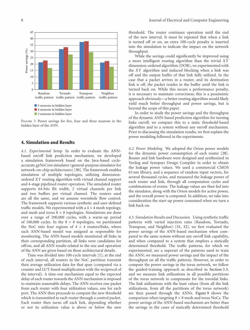
3.7. ANN Hardware Optimization and Trade-Offs. In orderto make the ANN architecture simpler and smaller westudied how the number of neurons of the hidden layeraffect the total power savings of the system. Given that the4 × 4 ANN monitors 16 routers, we need at least 8 inputneurons [14]. Having eight neurons at the input layer of theANN means that the hidden layer should have five neurons(based on the rule of thumb that a satisfactory numberof the hidden layer neurons equals to half the number ofinput neurons plus one neuron) [14]. Three different ANNswere developed with five, four, and three neurons at thehidden layer, respectively. Figure 7 shows the power savingsfor these ANNs under the use of four different traffic patterns(Random, Tornado, Transpose, and Neighbor). Using fourneurons therefore (instead of five), in the hidden layerexhibits the best power savings for all the traffic patterns.In addition, we studied how the bit representation of thetraining weights affects the threshold computation andsubsequently the total power savings. Figure 8 shows howthe bits used in representing the training weights influencethe power savings of the system. As we can see 24, 16, 8,and 6 bits show similar power savings, but these savings aresignificantly reduced when 4 bits are used, due to reducedtraining accuracy. Based on the above, we selected the weightbit representation from 6 bits, which made the multiplier-accumulation hardware very small, requiring a 6-bit port foreach weight and a 5-bit port for the utilization values.
8 Journal of Electrical and Computer Engineering
0
5
10
15
20
25
30
35
40
45
Random traffic pattern
Tornado traffic pattern
Transpose traffic pattern
Neighbor traffic pattern
5 neurons in hidden layer4 neurons in hidden layer3 neurons in hidden layer
Pow
er s
avin
gs (
%)
Figure 7: Power savings for five, four and three neurons in thehidden layer of the ANN.
4. Simulation and Results
4.1. Experimental Setup. In order to evaluate the ANN-based on/off link prediction mechanism, we developeda simulation framework based on the Java-based cycle-accurate gpNoCsim simulator (general-purpose simulator fornetwork-on-chip architectures) [30]. The framework enablessimulation of multiple topologies, utilizing dimension-ordered XY routing algorithm with virtual channel supportand 4-stage pipelined router operation. The simulated routersupports 64-bits flit width, 2 virtual channels per linkand two buffers per virtual channel. The routers usedare all the same, and we assume wormhole flow control.The framework supports various synthetic and user-definedtraffic models. We experimented with a 4× 4 mesh topology,and mesh and torus 8 × 8 topologies. Simulations are doneover a range of 200,000 cycles, with a warm-up periodof 100,000 cycles. In the 8 × 8 topologies, we partitionedthe NoC into four regions of 4 × 4 routers/links, whereeach ANN-based model was assigned as responsible formonitoring. The ANN-based models monitored all links intheir corresponding partition, all links were candidates foroff/on, and all ANN results related to the size and operationof the ANN are given based on these architectural details.
Time was divided into 100-cycle intervals [1]; at the endof each interval, all routers in the NoC partition transmittheir average utilization data for that span (computed via acounter and LUT-based multiplication with the reciprocal ofthe interval). A time-out mechanism equal to the expecteddelay of each router towards the ANN mechanism is imposedto maintain reasonable delays. The ANN receives one packetfrom each router with four utilization values, one for eachport. The ANN then proceeds to compute the new thresholdwhich is transmitted to each router through a control packet.Each router then turns off each link, depending whetheror not its utilization value is above or below the new
threshold. The router continues operation until the endof the new interval. It must be repeated that when a linkis turned off or on, an extra 100-cycle penalty is insertedinto the simulation to indicate the impact on the networkthroughput.
While the savings could significantly be improved usinga more intelligent routing algorithm than the trivial XYdimension-ordered algorithm (DOR), we experimented withthe XY algorithm and induced blocking when a link wasoff and the output buffer of that link fully utilized. In thecase that a packet arrives in a router, and its destinationlink is off, the packet resides in the buffer until the link isturned back on. While this incurs a performance penalty,it is necessary to maintain correctness; this is a pessimisticapproach obviously—a better routing algorithm would likelyyield much better throughput and power savings, but isbeyond the scope of this paper.
In order to study the power savings and the throughputof the dynamic ANN-based prediction algorithm for turninglinks on/off, we compare this to a static threshold-basedalgorithm and to a system without any on/off mechanism.Prior to discussing the simulation results, we first explain thepower modeling followed in the experiments.
4.2. Power Modeling. We adopted the Orion power modelsfor the dynamic power consumption of each router [28].Router and link hardware were designed and synthesized inVerilog and Synopsys Design Compiler in order to obtainthe leakage power values. We used a commercial CMOS65 nm library, and a sequence of random input vectors, forseveral thousand cycles, and measured the leakage power ofeach router and link, through all computation cycles andcombinations of events. The leakage values are then fed intothe simulator, along with the Orion models for active power,and the overall power is computed. In addition, we take intoconsideration the start-up power consumed when we turn alink back on.
4.3. Simulation Results and Discussion. Using synthetic trafficpatterns with varied injection rates (Random, Tornado,Transpose, and Neighbor) [31, 32], we first evaluated thepower savings of the ANN-based mechanism when com-pared to the same system without any on/off link capability,and when compared to a system that employs a staticallydetermined threshold. The traffic patterns, for which weexperimented, are a superset of the patterns used to trainthe ANN; we measured power savings and the impact of thethroughput on all the traffic patterns. However, in order tocompute the power savings in the torus network, we followthe guided-training approach as described in Section 3.3,and we measure link utilizations in all possible partitionsof the torus network to compensate for the toroidal links.The link utilizations with the least values (from all the linkutilizations, from all the partitions of the torus network)are then passed through the ANNs. Figure 9 shows thecomparison when targeting 8× 8 mesh and torus NoCs. Thepower savings of the ANN-based mechanism are better thanthe savings in the cases of statically determined threshold

Journal of Electrical and Computer Engineering 9
RandomTornado
TransposeNeighbor
0
5
10
15
20
25
30
35
40
45
Pow
er s
avin
gs (
%)
ANN-based 8×8
ANN-based 8×8
ANN-based 8×8 ANN-based 8×8 ANN-based 8×8 mesh 24 bits mesh 16 bits mesh 8 bits mesh 6 bits mesh 4 bits
Figure 8: Power savings for different training weight bit representations.
Random traffic patternTornado traffic pattern
Transpose traffic patternNeighbor traffic pattern
Statically-determined ANN-based8× 8
Statically-determined8×8 torus
ANN-based8×8 torus
0
5
10
15
20
25
30
35
40
45
Pow
er s
avin
gs (
%)
mesh8× 8 mesh
Figure 9: Power Savings for 8 × 8 mesh and 8 × 8 torus networks for the ANN-based technique, static threshold technique and no on/offtechnique.
and the case without any on/off links. The ANN-basedmechanism can identify a significant amount of future be-havior in the observed traffic patterns; therefore, it can intel-ligently select the threshold necessary for the next timinginterval.
Next, we measure the impact of the throughput in eachmechanism; while having no on/off mechanism obviouslyyields a higher throughput, the ANN-based technique showsbetter throughput results compared to statically deter-mined threshold techniques. Figure 10 shows the throughput

10 Journal of Electrical and Computer Engineering
0 .5
0 .55
0 .6
0 .65
0 .7
0 .75
0 .8
0 .85
Nor
mal
ized
th
rou
gpu
t
No on/off×8
torus8×8torus
Statically determined 8×8
torus
No on/off support8×8mesh
8×8mesh
Statically determined 8×8
mesh
Throughput
Random TornadoTranspose Neighbor
support—8ANN—based ANN—based
Figure 10: Average network throughput comparisons for 8× 8 mesh and torus networks.
Table 1: Power savings/hardware overhead comparisons.
Related work CharacteristicsPower savings
comparing to noalgorithm
Hardware overhead
[1]8× 8 2D mesh topology,
Uniform traffic∼37,5%—turning on/off
2 links per routerN/A
[11]8× 8 2D mesh topology,Pareto distribution—0.5
packet injection rate∼30%
500 equivalent logicgates per router port
Delay ignored
Proposed ANN-basedtechnique
8× 8 2D mesh topologyand 8× 8 torus
topology,uniform traffic
Up to ∼40%—turningon/off links based on
ANN prediction
4% of the NoC hardwarefor a complete 4× 4
Mesh NoC
comparisons for an 8 × 8 mesh and an 8 × 8 torus network.The throughput values are normalized based on the numberof the simulation cycles.
Figure 11 represents the normalized energy consumed ina 8× 8 mesh network. We observe that the energy consumedusing the ANN mechanism is less than the cases of statically-computed threshold and without on/off link managementalgorithm. The ANN exhibits a reduction in the overallenergy, because of a balanced performance-to-power savingsratio, when compared to not having on/off links or whencompared to static threshold computation.
Figure 12 presents the average packet delay in packets percycle for the 8 × 8 mesh, when the ANN-based mechanismis used compared to the cases where no on/off mechanism is
used and the statically computed threshold case. The ANN-based mechanism incurs more delay, but we believe that thedelay penalty is acceptable when compared to the associatedpower savings.
4.4. ANN Hardware Overheads: Synthesis Results. To com-pute the hardware overheads of the proposed scheme,the ANN-based mechanism for one 4 × 4 NoC regionwas synthesized and implemented targeting a commercial65 nm CMOS technology. The ensuing synthesized ANN-based controller and the associated hardware overheads ineach router consume approximately 4 K logic gates (forcomparison purposes, an NoC router similar to the oneused in our simulation [29] consumes roughly 21 K gates),

Journal of Electrical and Computer Engineering 11
0
1
20000 40000 60000 80000 100000
No on-off support 8×ANN-based 8×Statically determined 8×
Nor
mal
ized
en
ergy
Cycles (time slots)
0.2
0.4
0.6
0.8
1.2
8—torus8—torus
8—torus
Figure 11: Energy consumption for a 8× 8 mesh network.
50
60
70
80
90
100
110
Random Tornado Transpose Neighbor
ANN-based 8× 8 meshStatically determined 8× 8 meshNo on/off links mechanism 8× 8 mesh
Ave
rage
pac
ket
late
ncy
(cl
ock
cycl
es)
Figure 12: Average packet latency for the cases where ANN-basedmechanism is used, when trivial case is used and when there is noon/off mechanism.
bringing the estimated hardware overhead for an 4× 4 meshnetwork to roughly 4% of the NoC hardware.
4.5. Comparison with Related Works. Lastly, we briefly give acomparison with relevant related works that follow dynamicthreshold techniques in Table 1. When compared to both[1, 11], the ANN-based prediction yields better powersavings than having no prediction mechanism, while stillmaintaining lower hardware overheads. We must note thatwhile [10] was the motivating idea behind our paper, itpresented only a preliminary implementation of the idea,without enough information about hardware overheads andpower savings in order to make an informed comparison.
5. Conclusions
This paper presented how an ANN-based mechanism canbe used to dynamically compute a utilization threshold, thatcan be in turn used to select candidate links for turningon or off, in an effort to achieve power savings in an NoC.The ANN-based model utilizes very low hardware resources,and can be integrated in large mesh and torus NoCs,exhibiting significant power savings. Simulation resultsindicate approximately 13% additional power savings whencompared to a statically determined threshold methodologyunder synthetic traffic models. We hope to expand the resultsof this paper to further explore dynamic reduction of powerconsumption in NoCs using ANNs and other intelligentmethods.
References
[1] V. Soteriou and L.-S. Peh, “Dynamic power managementfor power optimization of interconnection networks usingon/off links,” in Proceedings of the 11th Symposium on HighPerformance Interconnects, pp. 15–20, 2003.
[2] F. Worm, P. Thiran, P. Ienne, and G. De Micheli, “An adaptivelow-power transmission scheme for on-chip networks,” inProceedings of the 15th International Symposium on SystemSynthesis, pp. 92–100, October 2002.
[3] S. Kumar, A. Jantsch, J.-P Soininen et al., “A network on chiparchitecture and design methodology,” in Proceedings of theIEEE Computer Society Annual Symposium on VLSI, pp. 117–124, 2002.
[4] L. Benini and G. De Micheli, “Networks on chips: a new SoCparadigm,” Computer, vol. 35, no. 1, pp. 70–78, 2002.
[5] K. Govil, E. Chan, and H. Wasserman, “Comparing algorithmsfor dynamic speed-setting of a low-power CPU,” in Proceedingsof the 1st Annual International Conference on Mobile Comput-ing and Networking, pp. 13–25, November 1995.
[6] V. Soteriou and L. S. Peh, “Exploring the design space of self-regulating power-aware on/off interconnection networks,”IEEE Transactions on Parallel and Distributed Systems, vol. 18,no. 3, pp. 393–408, 2007.
[7] Y. Hoskote, S. Vangal, S. Dighe et al., “Teraflops PrototypeProcessor with 80 Cores,” Microprocessor Technology Labs,Intel Corporation.
[8] W.-C. Cheng and M. Pedram, “Low power techniques foraddress encoding and memory allocation,” in Proceedings ofthe Asia and South Pacific Design Automation Conference (ASP-DAC ’01), pp. 245–250, 2001.
[9] D. Shin and J. Kim, “Power-aware communication optimiza-tion for networks-on-chips with voltage scalable links,” inProceedings of the 2nd IEEE/ACM/IFIP International Con-ference on Hardware/Software Codesign and System Synthesis(CODES+ISSS ’04), pp. 170–175, September 2004.
[10] T. Simunic and S. Boyd, “Managing power consumption innetworks on chips,” in Proceedings of the Design, Automationand Test in Europe, pp. 110–116, 2002.
[11] L. Shang, L.-S. Peh, and N. K. Jha, “Dynamic voltagescaling with links for power optimization of interconnectionnetworks,” in Proceedings of the International Symposium onHigh Performance Computer Architecture, pp. 91–102, 2003.
[12] Semiconductor Industry Association, “International Technol-ogy Roadmap for Semiconductors,” 2009, http://www.itrs.net/Links/2009ITRS/Home2009.htm.

12 Journal of Electrical and Computer Engineering
[13] A. K. Jain, J. Mao, and K. M. Mohiuddin, “Artificial neuralnetworks: a tutorial,” Computer, vol. 29, no. 3, pp. 31–44, 1996.
[14] R. Schalkoff, Artificial Neural Networks, McGrow-Hill, 1997.[15] A. Savva, T. Theocharides, and V. Soteriou, “Intelligent on/off
link management for on-chipnetworks,” in Proceedings of theIEEE Annual Symposium on VLSI, pp. 343–344, 2011.
[16] R. Marculescu, U. Y. Ogras, L. S. Peh, N. E. Jerger, and Y.Hoskote, “Outstanding research problems in NoC design:system, microarchitecture, and circuit perspectives,” IEEETransactions on Computer-Aided Design of Integrated Circuitsand Systems, vol. 28, no. 1, pp. 3–21, 2009.
[17] G. Chen, F. Li, M. Kandemir, and M. J. Irwin, “Reducing NoCenergy consumption through compiler-directed channel volt-age scaling,” in Proceedings of the ACM SIGPLAN Conferenceon Programming Language Design and Implementation (PLDI’06), pp. 193–203, June 2006.
[18] T. Pering, T. Burd, and R. Brodersen, “Voltage scheduling inthe IpARM microprocessor system,” in Proceedings of the 2000Symposium on Low Power Electronics and Design (ISLPED ’00),pp. 96–101, July 2000.
[19] F. Li, G. Chen, and M. Kandemir, “Compiler-directed volt-age scaling on communication links for reducing powerconsumption,” in Proceedings of the IEEE/ACM InternationalConference on Computer-Aided Design (ICCAD ’05), pp. 455–459, November 2005.
[20] V. Soteriou, N. Eisley, and L.-S. Peh, “Software-directedpower-aware interconnection networks,” ACM Transactions onArchitecture and Code Optimization, vol. 4, no. 1, pp. 274–285,2007.
[21] E. Y. Chung, L. Benini, and G. De Micheli, “Contents provider-assisted dynamic voltage scaling for low energy multimediaapplications,” in Proceedings of the International Symposium onLow Power Electronics and Design, pp. 42–47, August 2002.
[22] J. Kim and M. Horowitz, “Adaptive supply serial links withsub—1V operation and per-pin clock recovery,” in Proceedingsof the International Solid State Circuits Conference (ISSCC ’02),pp. 1403–1413, 2002.
[23] M. Alonso, S. Coll, J. M. Martınez, V. Santonja, P. Lopez, andJ. Duato, “Power saving in regular interconnection networks,”Parallel Computing, vol. 36, no. 12, pp. 696–712, 2010.
[24] S. Conner, S. Akioka, M. J. Irwin, and P. Raghavan, “Linkshutdown opportunities during collective communications in3-D torus nets,” in Proceedings of the 21st International Paralleland Distributed Processing Symposium (IPDPS ’07), pp. 1–8,March 2007.
[25] C. Jackson and S. J. Hollis, “Skip-links: a dynamically reconfig-uring topology for energy-efficient NoCs,” in Proceedings of the12th International Symposium on System-on-Chip 2010 (SoC’10), pp. 49–54, September 2010.
[26] R. Mullins, “Minimising dynamic power consumption in on-chip networks,” in Proceedings of the International Symposiumon System-on-Chip (SoC ’06), pp. 1–4, November 2006.
[27] M. Ali, M. Welzl, and S. Hellebrand, “A dynamic routingmechanism for network on chip,” in Proceedings of the 23rdNORCHIP Conference, pp. 70–73, November 2005.
[28] H.-S. Wang, X. Zhu, L.-S. Peh, and S. Malik, “Orion: a power-performance simulator for interconnection networks,” in Pro-ceedings of the International Symposium on Microarchitecture,pp. 294–305, 2002.
[29] E. Kakoullit, V. Soteriou, and T. Theocharides, “An artificialneural network-based hotspot prediction mechanism forNoCs,” in Proceedings of the IEEE Computer Society AnnualSymposium on VLSI (ISVLSI ’10), pp. 339–344, July 2010.
[30] H. Hossain, M. Ahmed, A. Al-Nayeem, T. Z. Islam, andM. M. Akbar, “gpNoCsim—a general purpose simulator for
network-on-chip,” in Proceedings of the International Confer-ence on Information and Communication Technology (ICICT’07), pp. 254–257, March 2007.
[31] W. J. Dally and B. Towles, Principles and Practices of Inter-connection Networks, Morgan Kaufmann, San Francisco, Calif,USA, 2004.
[32] J. Duato, S. Yalamanchili, and L. M. Ni, InterconnectionNetworks: An Engineering Approach, Morgan Kaufmann, SanFrancisco, Calif, USA, 2003.
Hindawi Publishing CorporationJournal of Electrical and Computer EngineeringVolume 2012, Article ID 537286, 12 pagesdoi:10.1155/2012/537286
Research Article
A Buffer-Sizing Algorithm for Network-on-Chipswith Multiple Voltage-Frequency Islands
Anish S. Kumar,1 M. Pawan Kumar,1 Srinivasan Murali,2 V. Kamakoti,1
Luca Benini,3 and Giovanni De Micheli4
1 Indian Institute of Technology Madras, Chennai 600036, India2 iNoCs, 1007 Lausanne, Switzerland3 University of Bologna, 40138 Bologna, Italy4 EPFL, 1015 Lausanne, Switzerland
Correspondence should be addressed to Anish S. Kumar, [email protected]
Received 17 July 2011; Accepted 1 November 2011
Academic Editor: An-Yeu Andy Wu
Copyright © 2012 Anish S. Kumar et al. This is an open access article distributed under the Creative Commons AttributionLicense, which permits unrestricted use, distribution, and reproduction in any medium, provided the original work is properlycited.
Buffers in on-chip networks constitute a significant proportion of the power consumption and area of the interconnect, and hencereducing them is an important problem. Application-specific designs have nonuniform network utilization, thereby requiringa buffer-sizing approach that tackles the nonuniformity. Also, congestion effects that occur during network operation need tobe captured when sizing the buffers. Many NoCs are designed to operate in multiple voltage/frequency islands, with interislandcommunication taking place through frequency converters. To this end, we propose a two-phase algorithm to size the switchbuffers in network-on-chips (NoCs) considering support for multiple-frequency islands. Our algorithm considers both the staticand dynamic effects when sizing buffers. We analyze the impact of placing frequency converters (FCs) on a link, as well as packand send units that effectively utilize network bandwidth. Experiments on many realistic system-on-Chip (SoC) benchmark showthat our algorithm results in 42% reduction in amount of buffering when compared to a standard buffering approach.
1. Introduction
In modern SoC designs, power consumption is a criticaldesign constraint as they are targeted as low-power devices.To achieve this, SoC designs employ power gating, wherethe cores are shutdown when they are unused. Instead ofshutting down each core, certain techniques cluster cores intovoltage and frequency (VF) islands, and when all the cores inan island are unused, the entire VI is shut down. The coresin a single VI have same operating voltage but can operate atdifferent frequencies. Running cores at different frequenciesis an effective method to trade off performance and powerconsumption.
Scalable on-chip networks, network-on-chips (NoCs),have evolved as the communication medium to connect theincreasing number of cores and to handle the communi-cation complexity [1–3]. With designs having multiple VFislands, the interconnect can reside in a separate island.By clustering the NoC into a single island, routing the
VDD and ground lines across the chip becomes difficult.Instead, the NoC is spread across the entire chip withdifferent components of the network operating at differentvoltage/frequency. If the core in an island is operating in adifferent frequency than the switch to which it is connected,the NI does the frequency conversion, and when a switchfrom one island is connected to another switch in a differentisland, frequency converters (FCs), such as the ones in [4, 5],are used to do the frequency conversion. Even if the twoswitches are operating at same frequencies, there might beclock skew for which synchronization is required.
In an NoC, a packet may be broken down into multipleflow control units called flits, and NoC architectures have theability to buffer flits inside the network to handle contentionamong packets for the same resource link or switch port.The buffers at the source network interfaces (NIs) are usedto queue up flits when the network-operating frequency isdifferent from that of the cores or when there is congestioninside the network that reaches the source. NoCs also employ
2 Journal of Electrical and Computer Engineering
Slowswitch
Fastswitch
Cycle Flits
F1
F2
Flits
F3
F1F2F3
Cycle
0
0123
12
3
4
5
300 MHz 600 MHz
Figure 1: Bubbles generated moving from slow to fast clock.
some flow control strategy that ensures flits are sent fromthe switch (NI) to another switch (NI) only when there areenough buffers available to store them in the downstreamcomponent.
In many NoCs, a credit-based flow control mechanism isused to manage transfer of flits at full throughput. In thisscheme the upstream router keeps a count of the numberof free buffers in the downstream router. Each time a flit iscommunicated from an upstream router and is consumed bythe downstream router, the credit counter is decremented.Once the downstream router forwards the flit and frees abuffer, a credit is sent to the upstream router and henceincrementing the credit count.
The network buffers account for a major part of thepower and area overhead of the NoC in many architectures.For example, in [6], the buffers account for more than50% of the dynamic power consumption of the switches. Amajor application domain for NoCs is in mobile and wirelessdevices, where having a low-power consumption is essential.Thus, reducing the buffering overhead of the NoC is animportant problem.
As such NoCs are targeted for specific applications, thebuffers and other network resources can be tuned to meet theapplication bandwidth and latency constraints. Several ear-lier works have dealt with application-specific customizationof various NoC parameters, such as the topology, frequencyof operation, and network paths for traffic flows [7–9]. Infact, several works have also addressed the customizationof NoC buffers to meet application constraints [10, 11].Many of the existing works utilize methods such as queuingtheory and network calculus to account for dynamic queuingeffects. While such methods could be used to compute thebuffer sizes quickly, they have several limitations in practice.Most queuing theory-based works require the input trafficinjection to follow certain probabilistic distributions, such asthe Poisson arrival process. Other schemes require regulationof traffic from the cores, which may not be possible in manyapplications (details given in the next section).
Although these methods can be used for fast designspace exploration, for example, during topology synthesis,final buffer allocation needs to consider simulation effectsto accurately capture the congestion effects. In this paper,we present a simulation-based algorithm for sizing NoC
buffers for application traffic patterns. We present a two-phase approach. In the first phase, we use mathematicalmodels based on static bandwidth and latency constraintsof the application traffic flows to minimize the buffers usedin the different components based on utilization. In thesecond phase, we use an iterative simulation-based strategy,where the buffers are increased from the ideal minimalvalues in the different components, until the bandwidth andlatency constraints of all the traffic flows are met duringsimulations. While in some application domains, such as inchip multiprocessors (CMPs), it is difficult to characterize theactual traffic patterns that occur during operation at designtime, there are several application domains (such as mobile,wireless) where the traffic pattern is well behaved [12]. Ourwork targets such domains where the traffic patterns canbe precharacterized at design time and a simulation-basedmechanism can be effective.
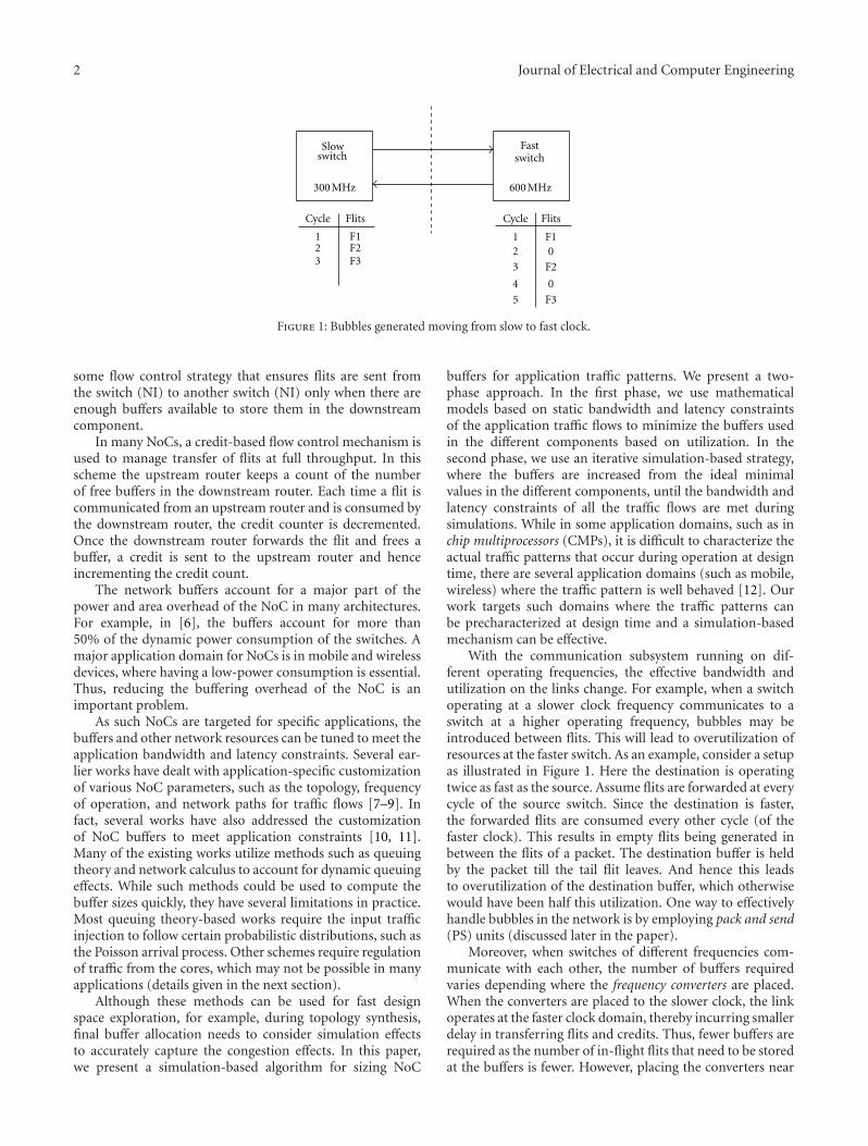
With the communication subsystem running on dif-ferent operating frequencies, the effective bandwidth andutilization on the links change. For example, when a switchoperating at a slower clock frequency communicates to aswitch at a higher operating frequency, bubbles may beintroduced between flits. This will lead to overutilization ofresources at the faster switch. As an example, consider a setupas illustrated in Figure 1. Here the destination is operatingtwice as fast as the source. Assume flits are forwarded at everycycle of the source switch. Since the destination is faster,the forwarded flits are consumed every other cycle (of thefaster clock). This results in empty flits being generated inbetween the flits of a packet. The destination buffer is heldby the packet till the tail flit leaves. And hence this leadsto overutilization of the destination buffer, which otherwisewould have been half this utilization. One way to effectivelyhandle bubbles in the network is by employing pack and send(PS) units (discussed later in the paper).
Moreover, when switches of different frequencies com-municate with each other, the number of buffers requiredvaries depending where the frequency converters are placed.When the converters are placed to the slower clock, the linkoperates at the faster clock domain, thereby incurring smallerdelay in transferring flits and credits. Thus, fewer buffers arerequired as the number of in-flight flits that need to be storedat the buffers is fewer. However, placing the converters near

Journal of Electrical and Computer Engineering 3
the slower clock leads to higher power consumption on thelinks as they are operating at a higher frequency. This effectalso needs to be considered during sizing of buffers.
In this paper, we present a buffer-sizing algorithm forapplication-specific NoCs having multiple VF islands. Weconsider a complex mobile benchmark to validate the buffer-sizing algorithm presented. We also analyze the effect ofplacement of frequency converters on the buffer size. Ourresults show that there is 42% reduction in the buffer budgetsfor the switches, on an average. Based on the models from[6], this translates to around 35% reduction in the overallpower consumption of the NoC switches. We also apply theapproach on a variety of system-on-chip (SoC) benchmarks,which show a significant 38% reduction in buffer budget.Also, we study the impact of pack and send units on thebuffer utilization. Results show that the PS units have a betterutilization of network resources.
2. Related Work
A lot of work has gone into proposing techniques for scalingthe voltage and frequencies of different IP cores on a chip.The authors of [13] propose techniques to identify optimalvoltage and frequencies levels for a dynamic voltage andfrequency scaling (DVFS) chip design. In [14] the authorspropose methods of clustering cores into islands, and DVFSis applied for these islands. In our work, we assume suchclustering of cores and NoC components as a part of thearchitecture specifications. In [15] the authors identify thetheoretical bounds on the performance of DVFS based onthe technology parameters.
With such partitioning of cores into VF islands becomingprevalent, globally asynchronous- and locally synchronous-(GALS-) based NoC designs have become the de factointerconnect paradigm. In [16] the authors propose analgorithm to synthesize an NoC topology that supports VFislands. This is one of the first approachs to design an NoCconsidering the support for shutting down of VF islands.The output of this algorithm can serve as input to ourapproach. In [17], the authors propose an reconfigurableNoC architecture to minimize latency and energy overheadunder a DVFS technique. In [18], the authors proposeasynchronous bypass channels to improve the performanceof DVFS enabled NoC.
In this work we extend the proposed buffer-sizingalgorithm to designs with VF islands to optimize NoC powerand area while meeting the design requirements. Sizingbuffers is critical for reducing the power and area footprintof an NoC.
In [10], the authors proposed an iterative algorithmto allocate more buffers for the input ports of bottleneckchannels found using analytical techniques and also pro-posed a model to verify the allocation. The model assumesthe Poisson arrival of packets. In [19], buffer sizing forwormhole-based routing is presented, also assuming thePoisson arrival of packets. The problem of minimizingthe number of buffers by reducing the number of virtualchannels has been addressed in [20] assuming that inputtraffic follows certain probabilistic distributions. In [21],
a queuing theory-based model to size the number of virtualchannels is proposed by performing a chromosome encodingof the problem and solving it using standard geneticalgorithm, again assuming the Poisson arrival of packets. Theauthors of [22] proposed an analytical model to evaluatethe performance of adaptively routed NoCs. This work againassumes the Poisson arrivals for the flows. In [23] the authorsproposed a probabilistic model to find the average bufferutilization of a flow accounting for the presence of otherflows across all ports. The authors of [24] used an approachto minimize buffer demand by regulating traffic through adelayed release mechanism and hence achieving the goal ofappropriate buffer sizing. Unlike all these earlier works, wemake no assumption on the burstiness of input traffic andthe arrival pattern for packets.
In [25], the authors propose an algorithm to size thebuffers, at the NIs, using TDMA and credit-based flowcontrol. This work is complimentary to ours, as the authorstarget designing NI buffers to match the different rate ofoperation of cores and the network. A trace-driven approachto determine the number of virtual channels is presented in[26]. While the notion of simulation-driven design method isutilized in the work, the authors do not address the sizing ofbuffers. Our buffer-sizing methods are significantly differentfrom methods for virtual channel reduction, as we needa much more fine grained control on buffer assignment.Towards this end, we present an iterative approach to buffersizing that utilizes multiple simulation runs.
3. Design Approach
In this section, we give a detailed explanation of the designapproach used for buffer sizing. The approach is presented inFigure 2. We use a two-phase method: static sizing, involvingconstraint solving, followed by a simulation-based approach.
We obtain two sets of inputs for the buffer-sizingapproach: application and architecture specifications. Theapplication specifications include the bandwidth and latencyconstraints for the different flows. The architecture specifica-tions include the NoC topology designed for the application,routes for the traffic flows, the number of voltage/frequencyislands, and flit width of the NoC.
We have the following assumptions about the architec-ture and application.
(i) For illustrative purposes, we consider input-queuedswitches for buffer sizing. In fact, the algorithmpresented in generic and can be easily extended tooutput-queued (and hybrid) switches as well.
(ii) We define the term number of buffers used at a portto be the number of flits that the buffers can store atthat port.
(iii) A wormhole, credit-based flow control is assumed inthe NoC, which is widely used.
(iv) We do not explicitly consider the use of virtual chan-nels. The algorithm, in fact, can be easily applied toarchitectures that support multiple virtual channelsas well.

4 Journal of Electrical and Computer Engineering
Latency constraintsbandwidth constraints
Topology, routes,flit width,
operating frequencies,VF islands
Place frequency convertersidentify link latency
add pack and send units
Compute static buffer sizes
Run simulation
Phase 1
Phase 2
Iterative buffer sizing
Figure 2: Buffer sizing design approach.
(v) We assume a uniform flit width across the wholenetwork, which is again commonly observed in manyNoCs.
(vi) We apply the buffer-sizing algorithm for a singleapplication. In many designs, multiple applicationscan be run on the same device. The extension of thebuffer-sizing method to support multiple applicationscenarios is similar to the extension of topology syn-thesis methods to consider multiple applications andhas been thoroughly addressed by several researchersbefore [27]. Hence, we only show the core methodapplicable for a single application here.
The output of the buffer-sizing algorithm is the numberof flit buffers at each input port of the different switches. Weonly perform the sizing of the switch buffers, and we refer thereader to earlier works on sizing NI buffers that consider thedifferent rates of the cores and the network [25].
The algorithm phases are as follows.
Phase 1 (Static Sizing). To achieve full throughput andutilization on all the switches and links, the credit-basedflow control mechanism requires a minimum number ofbuffers that depends on the number of cycles to traverse thelinks. In an application-specific topology, many parts of thenetwork can have much less than 100% utilization. In thisfirst phase, we formulate mathematical models relating thebuffering at a port with the bandwidth utilization of the portand capturing latency constraints of traffic flows. We build alinear program- (LP-) based model to minimize the numberof buffers at a port based on the utilization at the port and torespect the latency constraints of all flows across the differentpaths.
Phase 2 ( Simulation-Based Sizing). In the second phase, weperform simulation of the NoC with the buffering valuesobtained from Phase 1. There are three important parame-ters of a traffic flow that significantly affect the congestion
behavior: the bandwidth of the flow, the burstiness, andthe number of flows overlapping at each link/switch port.While the static sizing mechanism considers the bandwidthof flows to compute utilization, the effects of burstinessand overlapping flows are considered during this secondphase. We run simulations and utilize methods to iterativelyincrease buffers at ports until the bandwidth and latencyconstraints of all flows are met.
4. Buffer Sizing
4.1. Basic Architecture. In this section, we formulate theproblem of buffer sizing.
We represent the communication constraints betweenthe cores using a core graph.
Definition 1. The core graph is a directed graph, G(V ,E)with vertex vi ∈ V representing the core and the directededge ei, j ∈ E connecting vertices vi and vj , representingthe communication link between the cores. The edge weight,commi, j , denotes the communication bandwidth between viand vj . The set F represents the set of flows between the cores.
An NoC graph denotes the NoC topology and thecapacity of the links in the topology.
Definition 2. The NoC graph is a directed graph, T(P,Q)with vertex pi ∈ P representing the switch and the directededge qi, j ∈ Q connecting the vertices pi and pj representingthe link connecting the switches. The edge weight, bwi, j ,denotes the link bandwidth or capacity available across piand pj .
Definition 3. Let the set of operating frequencies of variousdomains (in GHz) be denoted by the set D. Let freqency (i)be a mapping function that maps a chip component to thefrequency at which the domain is operating at:
frequency (i) : {V ,P} −→ D, i ∈ V ,P (1)

Journal of Electrical and Computer Engineering 5
CyclesCredit
1 2 3 4 5 6 7 82 2 1 2 1 2 2 3
Flit 1 ST
ST ST
LC
C
C
L
ST STL
ST
Flit 2
Flit 3
(a) With 3 buffers
Cycles
Credit
1 2 3 4 5 6 7 81 1 0 1 0 1 1 2
ST STC
C
C
L
ST STL
ST L STFlit 1
Flit 2
Flit 3
(b) With 2 Buffers
Figure 3: Timing diagram of two different buffer configurations. ST—switch traversal delay, L—link latency, C— credit latency.
When crossing VF islands, converters are required to dothe frequency conversion. For this purpose, we use FC unitsthat are basically dual-clocked FIFOs. The size of the FCsis uniform throughout the design. Most FCs incur a delaypenalty for traversal, which is typically few cycles of the slowclock [28]. We denote this latency by FC lat.
The latency of a link is the sum of the latency totraverse the FC and link traversal latency. The link traversallatency is defined by the frequency at which the link isoperated. Let unit len denote the distance in mm a signal cantraverse in 1ns. This can be determined based on the design’stechnology node. Then the latency of a link is given by
Ni, j = FC lat +1
freq× lengthi, j
unit len(2)
freq =⎧⎨⎩
frequency (i) FC near destination,
frequency(j)
FC near source,(3)
where freq denotes the operating frequency of the link and itdepends on where the FC is placed on the link, and lengthi, j
denotes the length of the link in mm.The bandwidth or capacity of a link is given by the
product of link width and frequency of operation of the link:
bwi, j = freq× link widthi, j . (4)
Definition 4. The links traversed by a flow, fk, ∀k ∈ F,connecting source sk and destination dk is represented by theset pathk.
The utilization Ui, j of a link qi, j is the sum of thebandwidths of all the flows using the link divided by thecapacity:
Ui, j =∑
l,m comml,m
bwi, j, ∀l,m, k,
s.t. qi, j ∈ Pathk, sk = vl, dk = vm.
(5)
We assume a pack and send (PS) unit that can be used tobetter utilize the network resource. A PS unit is a 1-packet-long buffer that holds an entire packet before forwarding itto the downstream buffer. Employing PS units changes theabove link utilization Ui, j .
The NoC architecture assumes a credit-based flow con-trol mechanism. The following is a lemma for the numberof buffers required in the downstream switch for credit-based flow control mechanism to support full throughputand utilization [29].
Lemma 5. For a link with delay N cycles, in credit-based flowcontrol, the number of flit buffers required at the downstreamrouter in order to get 100% throughput is at least (2N + 1).
The intuitive reasoning for this buffering value is asfollows. A flit takes N cycles to reach the next switchand, when it leaves the downstream buffer, the credit takesanother N cycles to reach back and it takes one more cycleto process the credit. Thus, the overall time delay betweensending a flit and processing the corresponding credit is(2N + 1). During that time, under full utilization, the samenumber of flits could be sent from the sender switch whichneeds buffering at the downstream switch.
When the link utilization is less than 100%, the down-stream router needs not have (2N + 1) buffers and can besized according to the utilization. The illustration in Figure 3shows that buffers in the downstream router can be less than(2N+1). In the example, two setups with downstream routerhaving 3 and 2 buffers and link latency of 1 cycle are shown.The flow is assumed to have a 50% link utilization with thepacket comprising of 1 flit. The packets are generated everyother cycle, hence having utilization of 50%. In Figure 3(a),the timing diagram for a setup with 3 buffers and the creditcounter value (available buffers at downstream router) ateach cycle are shown. The same throughput (50%) can beachieved with 2 (lesser than (2N + 1)) buffers (Figure 3(b)).However, when the number of buffers is reduced fromthe ideal values, the packet latencies increase. For example,consider a 4-flit packet in the above scenario with 2 buffers.Since, the buffers are reduced from the ideal, the flits canbe sent only every other cycle, and hence the packets havea latency of 7 cycles to be sent from the upstream to thedownstream switch. Thus, when reducing the buffer size, weshould also consider whether the latency constraints for theflows are met.
Table 1 summarizes the different parameters of thenetwork.
5. Static Buffer Sizing
The latency of a link in the network is defined by the rateat which the link is clocked. Without loss of generality, letus assume Ni, j to be the number of cycles needed to traversethe link qi, j . Then the minimum buffering required at a port,based on the utilization at the port, is given by
βi, j ≥(
2Ni, j + 1)∗Ui, j , (6)
6 Journal of Electrical and Computer Engineering
Table 1: Network parameters.
Parameter Description
V Set of IP cores
P Set of NoC switches
D Set of frequencies of VF islands
F Set of flows in the network
FC lat Latency of frequency converter
lengthi, j length of link in mm
Ni, j Link latency in cycles
Ui, j Link utilization
βi, j Buffer size at link qi, jpsk Packet size of flow k
LCk Latency constraint of flow k
where βi, j represents the buffers statically assigned at the portconnecting switches pi & pj ∈ P.
Let the latency constraint that needs to be met by aflow fk, which is obtained as part of the input applicationspecifications, be LCk. The latency of a flow depends on thesize of the buffers along its path and the size of packet (inflits). For the first flit of the packet, the latency is given bythe length of the path (hops), and for the consequent flits itis determined by the buffering available at the downstreamrouter. When buffering is less than the ideal value at an inputport that is connected to the link qi, j , the body (and tail) flitsmay need to wait at the upstream switch for credits to reachback. This delay for the flits at a link qi, j is given by
(2Ni, j + 1
)
βi, j× (psk − 1
), (7)
where psk denotes the number of flits in a packet.A packet encounters this delay at that part of the path
where the amount of buffering, when compared to the idealvalue, is lowest.
Under zero load conditions, the latency constraint on aflow is met if the following constraint is satisfied:
max∀i, j, s.t. qi, j ∈ Pathk
⎧⎨⎩
(2Ni, j + 1
)
βi, j× (psk − 1
)⎫⎬⎭ + Hk ≤ LCk,
(8)
where Hk denotes the hop count of the flow fk. The first termon the left-hand side accounts for the maximum delay acrossthe entire path due to the reduced buffering.
The problem of computing the minimum number ofbuffers required at the different ports to meet the bandwidth
and latency constraints can be formulated as a linear program(LP) as follows:
min :|P|∑
i=1
|P|∑
j=1
βi, j , i /= j,
s.t. βi, j ≥(
2Ni, j + 1)∗Ui, j ,
max∀i, j, s.t. qi, j ∈ Pathk
⎧⎨⎩
(2Ni, j + 1
)
βi, j× (psk − 1
)⎫⎬⎭ + Hk ≤ LCk
βi, j ≤(
2Ni, j + 1)
, βi, j ≥ 0, ∀i, j ∈ P.
(9)
The objective function to be minimized is the totalbuffering used in the switches. The bandwidth and latencyconstraints, obtained from (6) and (8), form the constraintsof the LP. The formulation can be solved quickly andefficiently by any linear/convex program solver, such as thelp solve [30]. Since the resulting buffer values by solvingthe LP can be fractional, we round up the value to thenext integer. In fact, we could have formulated the aboveequations as an integer linear program (ILP), where we canforce the buffer values to be integers. However, as solving theILP formulation has exponential time complexity, it will beunfeasible to apply in practice. Hence, we use the heuristic ofLP formulation with the rounding scheme.
6. Simulation-Based Buffer Sizing
After Phase 1, we perform simulation of the NoC usingthe computed buffer sizes and injecting packets to modelthe application communication patterns that are taken asinputs. The simulation-oriented approach is iterative, wherebuffers are added and simulations performed iteratively, untilall the flows meet the bandwidth and latency requirements.To perform the sizing, we propose two strategies called asuniform increment and flow-based increment.
In the first strategy, buffers at all the ports are incre-mented iteratively by a small step. The buffer increment at aport depends on the burstiness of the flows and the numberof flows contending for the same port. During simulations,the burst sizes of the flows at each port are tracked and theaverage burstiness of a flow is identified. The burstiness offlow fk is denoted as Bk.
We use the following term to increment the buffers at aport connected to the link qi, j at each iteration:
∑∀ fks.t.qi, j ∈ Pathk
α∗ Bk
max∀ fkBk ∗ |F| , (10)
where α is the parameter that is increased from 0 insmall steps with each simulation iteration. Intuitively, theincrement captures the burstiness of flows, scaled by themaximum burstiness of any flow of the application andthe summation captures the number of contending flows,normalized to the total number of flows in the application.Thus, ports that have many contending flows, or flows with

Journal of Electrical and Computer Engineering 7
Switch Switch
Frequencyconverter
Slow linkLess power
Fast domainSlow domain
Source Destination
Figure 4: Placed closer to the fast clock domain.
Switch Switch
Frequencyconverter
Fast linkHigher power
Fast domainSlow domain
Source Destination
Figure 5: Placed closer to the slow clock domain.
large burst sizes get a larger increment at each iteration. Thevalue of α is set experimentally. A very low value would resultin lot more solutions being explored, while requiring morenumbers of simulations.
In the second strategy, we track the flows that violate thebandwidth or latency constraints, and only the buffers alongthe path of such flows are incremented. This approach is anoptimization of the previous strategy, giving finer controlto access individual flows. For faster results, the uniformincrement scheme can be used, while for better results, theflow-based increment scheme can be used. Thus, the twoschemes allow a tradeoff between having fine control over thebuffer allocation and minimizing the number of simulationruns required. In Section 9, the results of the two proposedstrategies are discussed.
7. Placement of Frequency Converters
In this section the proposed buffer sizing scheme is extendedto designs with multiple VF islands. We assume that thearchitecture characteristics include the VF island informa-tion.
FCs are used when crossing clock domains. Several kindsof FCs are proposed in the literature, but the most commonlyused one is a dual clock FIFO (DCFIFO). A DCFIFOconsists of a series of shift registers connected together thatshift the input data from one domain to the output tothe other domain. The input is clocked by one clock andoutput is clocked by the other, and the data is stored in theintermediate registers till the output is ready to consume it.
From the input architectural specification, the clockdomains are identified and DCFIFOs are added along thelinks that cross the domains. Placement of the DCFIFOs is acritical design problem as they affect the power consumption
and buffering required, hence, the performance of theinterconnect.
7.1. Frequency Converters near Fast Domain. In this setup,the frequency converters are placed close to the fast clockdomain, as shown in Figure 4. By placing the convertersnear the fast clock, the link is clocked by the slower clock.From (2), it is evident that when the link operates at a lesserfrequency, the latency increases. But, since the operatingfrequency is lesser, the power consumed by the link is lesser,as P ∝ f . The increased latency of the link will demandthe downstream router to have more buffering (according toLemma 5).
7.2. Frequency Converters near Slow Domain. In this setup,the FCs are placed closer to the slow clock domain, therebyclocking the link by the faster clock, as shown in Figure 5.This makes the link to operate at higher speed, and hence thelatency is lesser (2), thereby reducing the buffering needed atthe downstream router. But the higher operating frequencymakes the link consumes more power.
This tradeoff between power consumed by the link andpower consumed because of extra buffering can be exploredto choose a specific design point that meets the systemrequirements. The effects of placement of FCs is analyzed,and the results are discussed in Section 9.3.
8. Handling Bubbles
In multiclock designs, inherently lot of empty flits aregenerated because of difference in the operating speed ofthe network components. Network flows traversing from afaster to slower frequency domain will incur higher latency,and enough buffering must be provided to meet the designconstraints.
On the other hand, network flows traversing from aslower to a faster clock domain create bubbles in the network.Since destination is faster than the source, empty flits(bubbles) are generated in the network which underutilizethe network resources. These bubbles must be reduced inorder to better utilize the resources, and employing packand send (PS) units can help in reducing them. Bubbles ina flow hold the buffers along the path for a long periodunnecessarily, and hence other flows contending for the linksare delayed. Waiting for the entire packet to arrive beforethe flow requests for the downstream buffer allows otherflows contending for the link to proceed. Pack and send unitholds the flits temporarily till the entire packet is formed,and then it is forwarded to the downstream router. Hence aPS unit contains buffers to hold an entire packet. Section 9.4discusses the results obtained when employing PS units.
9. Results
We consider a 26-core multimedia benchmark for a detailedstudy of the buffer-sizing algorithm. In Section 9.6, weshow the application of the algorithm to a variety ofbenchmarks. The system includes ARM, DSPcores, memorybanks, DMA engine, and several peripheral devices [31].

8 Journal of Electrical and Computer Engineering
0
10
20
30
40
50
10 20 30 40 50 60 70 80 90 100
Link utilization (%)
Nu
mbe
r of
flow
s
Figure 6: Histogram of link utilization.
We consider benchmarks with custom topologies, but thealgorithm is extendable to regular topologies too. Some ofthe benchmarks involve topologies with large number ofswitches (26 cores and 20 switches) which is similar to regulartopologies. For the initial study to validate the buffer-sizingalgorithm we consider no voltage and frequency domainsfor the network. The entire interconnect operates at a singlefrequency.
We use existing tools to synthesize NoC topologies withdifferent number of switches [9]. The flit width of theNoC is set to 32 bits. For each topology synthesized, weperform simulations with very large (40 buffers at eachport) buffer sizes and set the frequency of operation toa value where the application constraints are met duringsimulations. This ensures a working solution with very largebuffering values, and the objective is to reduce it to muchsmaller values. We chose 3 different topologies with few tolarge number of switches (3, 14, and 20 switches) for thestudy. The number of cycles needed to traverse the linksbetween the switches depend on the floor plan of the design,the technology library characteristics, and the operatingfrequencies of the components. For this study, we consider3 different configurations for the link delay: 1, 2, and 3 cyclesacross all the links. This allows us to show the effect of linkdelays on the efficiency of the proposed methods. We denotethe topology points by the number of switches, link delay.
9.1. Effects of Static Buffer Sizing. In the static sizing, wereduce the buffering at any port when the utilization atthe port is less than 100%. We observed that in this andmost other embedded benchmarks, the link utilization isvery nonuniform, and only some bottleneck links havehigh utilization while others have much lower values. Forexample, in Figure 6, we show the utilization of the differentlinks for a 20-switch benchmark. It can be seen that there area lot of flows that have a very low utilization of less than 10%.Hence, utilization-based sizing can lead to a large reductionin buffering. Please note that, due to protocol overhead, wecould not achieve 100% utilization on any link and neededto operate the network at a slightly higher frequency than theminimum needed to meet the bandwidth constraints.
0
50
100
150
200
250
300
350
400
450
500
550
3.1 14.1 20.1 3.2 14.2 20.2 3.3 14.3 20.3
Bu
ffer
siz
e (fl
its)
Benchmarks (Swt, Lnk latency)
Original
Static
Figure 7: Comparison of buffering schemes.
10
15
20
25
30
35
40
0 100 200 300 400 500
Avg
. lat
ency
(cy
cles
)
Buffer size (flits)
Uniform inc.Uniform bufferingFlow-based inc.
Figure 8: Latency versus buffering.
We show the effect of static sizing in Figure 7. Wecompare the results with an original uniform buffering,where the minimum number of buffers for full utilization isused at all the ports. We can see that the proposed schemeresults in large reduction in buffering requirements.
9.2. Effects of Simulation-Based Buffer Sizing. In this subsec-tion, we compare the application of the two strategies, uni-form increment and flow-based increment. For comparisonswe also developed a standard uniform buffering strategy,where all ports have the same number of buffers. This is setto the minimum value at which the latency and bandwidthconstraints of all the flows are met during simulations. Weconsider 3 different burst sizes for all the traffic flows: 4, 8,and 16 byte bursts.
Figure 8 shows the average latency across all the flowsfor a spectrum of buffer budgets for a benchmark with 3, 3design and a burst size of 16 for all the flows. Depending on
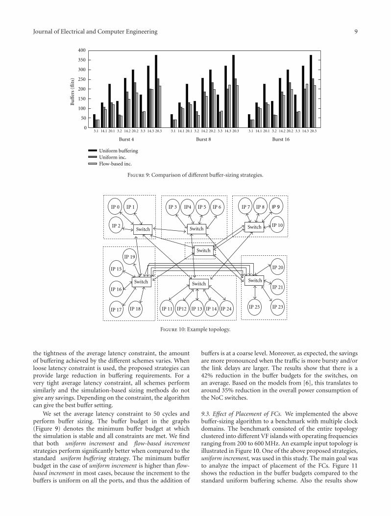
Journal of Electrical and Computer Engineering 9
03.1 14.1 20.1 3.2 14.2 20.2 3.3 14.3 20.3 3.1 14.1 20.1 3.2 14.2 20.2 3.3 14.3 20.3 3.1 14.1 20.1 3.2 14.2 20.2 3.3 14.3 20.3
50
100
150
200
250
300
350
400
20.3
Bu
ffer
s (fl
its)
Uniform inc.Flow-based inc.
Burst 16Burst 8Burst 4
Uniform buffering
Figure 9: Comparison of different buffer-sizing strategies.
IP 0 IP 1 IP 3
IP 19
IP 15
IP 16
IP 17 IP 18
IP4 IP 5 IP 6
IP 11 IP12 IP 13 IP 14 IP 24
IP 7 IP 8 IP 9
IP 10
IP 20
IP 21
IP 23IP 25
IP 2
Switch
SwitchSwitch
SwitchSwitchSwitch
Switch
Figure 10: Example topology.
the tightness of the average latency constraint, the amountof buffering achieved by the different schemes varies. Whenloose latency constraint is used, the proposed strategies canprovide large reduction in buffering requirements. For avery tight average latency constraint, all schemes performsimilarly and the simulation-based sizing methods do notgive any savings. Depending on the constraint, the algorithmcan give the best buffer setting.
We set the average latency constraint to 50 cycles andperform buffer sizing. The buffer budget in the graphs(Figure 9) denotes the minimum buffer budget at whichthe simulation is stable and all constraints are met. We findthat both uniform increment and flow-based incrementstrategies perform significantly better when compared to thestandard uniform buffering strategy. The minimum bufferbudget in the case of uniform increment is higher than flow-based increment in most cases, because the increment to thebuffers is uniform on all the ports, and thus the addition of
buffers is at a coarse level. Moreover, as expected, the savingsare more pronounced when the traffic is more bursty and/orthe link delays are larger. The results show that there is a42% reduction in the buffer budgets for the switches, onan average. Based on the models from [6], this translates toaround 35% reduction in the overall power consumption ofthe NoC switches.
9.3. Effect of Placement of FCs. We implemented the abovebuffer-sizing algorithm to a benchmark with multiple clockdomains. The benchmark consisted of the entire topologyclustered into different VF islands with operating frequenciesranging from 200 to 600 MHz. An example input topology isillustrated in Figure 10. One of the above proposed strategies,uniform increment, was used in this study. The main goal wasto analyze the impact of placement of the FCs. Figure 11shows the reduction in the buffer budgets compared to thestandard uniform buffering scheme. Also the results show

10 Journal of Electrical and Computer Engineering
100
0
200
300
400
500
600
700
800
Fast Slow Fast Slow Fast SlowBurst 4 Burst 8 Burst 12
Placement of freq. converters
Uniform bufferingα-based approach
Nu
mbe
r of
buff
ers
Figure 11: Placements of FCs.
that the buffering required when placing the FCs closer tothe slow domain is lesser than the buffering required whenplacing it close to fast domain. This however affects the linkpower, as the links are clocked higher and hence the linkpower is more. With smaller transistor sizes, the link poweris as significant as the logic power, and hence the powerconsumed by the links must also be taken into account.
9.4. Impact of Pack and Send. For studying the effect of packand send unit, the benchmark with multiple clock domainswas considered. Since the pack and send unit has an effectonly across links where the utilization is high, we scaled thefrequencies to a range of 500–900 MHz and the burstinesswas increased. For the study the proposed buffer-sizingalgorithm was used with PS units placed along links goingfrom slow to fast clock domain. The effect on buffering withand without pack and send unit was analyzed. Though the PSunits require extra buffers to hold a packet, results showedthat the total buffering required (including the PS buffers)remains the same. However the link utilization reduces whenusing PS units. Since there is lesser contention among theflows while using PS units, there is a direct impact in terms ofreduction in the buffering required at the switches. However,the total buffering required remains the same as the decreasein buffering at the switches is compensated by the extrabuffers required in the PS units. Figure 12 shows the overallaverage link utilization with and without PS unit. This showsthat the PS unit helps in better utilizing the resources, andthis reduction in link utilization can be directly converted topower savings at lower technology nodes.
9.5. Run Time of the Methods. Since Phase 1 uses LP formu-lation and not ILP, the solution is tractable and is obtainedquickly. Phase 1 of the algorithm finished in few seconds forall the benchmarks on a 2.66 GHz Linux Machine. Amongthe two strategies presented in Phase 2, there is a tradeoffbetween the running time of simulations and the granularity
30
40
50
60
70
80
4 8 16 32
Lin
k u
tiliz
atio
n (
%)
Burstiness
Without pack and sendWith pack and send
Figure 12: Pack and send.
of controlling buffer sizes. Previous sections show that thefine control of buffer sizes for flow based increment approachhelps in achieving a lower budget. But the running time toconverge to a budget is more. Each simulation run can takefrom 20 minutes to few hours, depending on how long a traceneeds to be simulated. The uniform increment approachtook 20–60 simulation runs, while the flow-based incrementapproach took 50–100 runs. Thus, the design time requiredcould be significantly higher for the flow-based incrementstrategy. The designer has the choice of the strategy and thestep used for the α values and can make a tradeoff betweenbuffer reduction and design time.
9.6. Experiments on Other Benchmarks. To show the gener-ality of the method, we consider 4 other SoC benchmarks:D 36 4, D 36 6, D 36 8, and D 35. The first 3 benchmarkshave 36 cores, with each communicating to 4, 6, and 8other cores respectively. The last benchmark has 35 cores andmodels bottleneck traffic communication, such as memorycontroller traffic. On average, the proposed schemes result in38% reduction in buffer sizes when compared to the standarduniform sizing schemes.
9.7. Comparison with Theoretical Models. To show that theproposed buffer-sizing methodology works for well-behavedtraffic also, we compare our results with queuing theory-based model proposed in [10]. Figure 13 shows that theproposed model is able to achieve buffer budgets close to thetheoretical limit proposed in the paper.
10. Conclusion
As buffers account for a large area, power overhead in NoCs,reducing the amount of buffering is an important problem.Buffer sizing is closely tied to dynamic congestion effects thatcan be observed only during simulations. Towards this end,

Journal of Electrical and Computer Engineering 11
0
20
40
60
80
100
120B
uff
er s
ize
(flit
s)
Benchmarks (Swt, Lnk latency)
Uniform inc.Flow-based inc.
Theoretical
3.1 14.1 20.1 3.2 14.2 20.2 3.3 14.3 20.3
Figure 13: Comparison with theoretical models.
in this paper, we present a two-phase algorithm for buffersizing. Our approach considers the nonuniformity in theutilization of the different parts of the network and uses asimulation-based iterative mechanism. Our results show alarge reduction in buffering required (42%) when comparedto standard buffering approach. The proposed buffer-sizingalgorithm was extended to designs with multiple clockdomains. Results showed a significant reduction in bufferbudget. We also analyzed the effect of placement of FCs onthe overall buffer budget. Also the use of PS units to handlebubbles in the network was studied, and results showed thatemploying them utilize resources better.
Future Work
In the proposed buffer-sizing approach, the second phasethat involves simulations is the step that consumes asignificant portion of the total run time. We can use intuitiveapproaches to reduce the simulation time for that step. Butthis is beyond the scope of this work and can be a part of anextension to this work.
Acknowledgments
The authors would like to acknowledge the ARTIST-DESIGNNetwork of Excellence. This work has also been supported bythe project NaNoC (project label 248972) which is (partly)funded by the European Commission within the ResearchProgramme FP7.
References
[1] L. Benini and G. De Micheli, “Networks on chips: a new SoCparadigm,” Computer, vol. 35, no. 1, pp. 70–78, 2002.
[2] G. D. Micheli and L. Benini, Networks on Chips: Technologyand Tools, Morgan Kaufmann, 2006.
[3] P. Guerrier and A. Greiner, “A generic architecture for on-chip packet switched interconnections,” in Proceedings of
the Design, Automation and Test in Europe, pp. 250–256,2000.
[4] R. W. Apperson, Z. Yu, M. J. Meeuwsen, T. Mohsenin, andB. M. Baas, “A scalable dual-clock FIFO for data transfersbetween arbitrary and haltable clock domains,” IEEE Trans-actions on Very Large Scale Integration Systems, vol. 15, no. 10,pp. 1125–1134, 2007.
[5] A. Strano, D. Ludovici, and D. Bertozzi, “A library of du-alclock fifos for cost-effective and flexible mpsoc design,”in Proceedings of the International Conference on EmbeddedComputer Systems (SAMOS ’10), pp. 20–27, 2010.
[6] S. Murali, T. Theocharides, N. Vijaykrishnan, M. J. Irwin, L.Benini, and G. De Micheli, “Analysis of error recovery schemesfor networks on chips,” IEEE Design and Test of Computers, vol.22, no. 5, pp. 434–442, 2005.
[7] J. Hu and R. Marculescu, “Exploiting the routing flexibilityfor energy/performance aware mapping of regular NoCarchitectures,” in Proceedings of the Design, Automation andTest in Europe, 2004.
[8] A. Hansson et al., “A unified approach to mapping and routingin a combined guaranteed service and best-effort Network-on-Chip architecture,” in Proceedings of the International Con-ference on Hardware/Software Codesign and System Synthesis,2005.
[9] S. Murali, P. Meloni, F. Angiolini et al., “Designing applica-tion-specific networks on chips with floorplan information,”in Proceedings of the International Conference on Computer-Aided Design (ICCAD ’06), pp. 355–362, November 2006.
[10] J. Hu and R. Marculescu, “Application-specific buffer spaceallocation for networks-on-chip router design,” in Proceedingsof the IEEE/ACM International Conference on Computer-AidedDesign, Digest of Technical Papers (ICCAD ’04), pp. 354–361,November 2004.
[11] Y. Yin and S. Chen, “An application-specific buffer allocationalgorithm for network-on-chip,” in Proceedings of the 8th IEEEInternational Conference on ASIC (ASICON ’09), pp. 439–442,October 2009.
[12] W. H. Ho and T. M. Pinkston, “A methodology for designingefficient On-Chip interconnects on well-behaved communi-cation patterns,” in Proceedings of the International Symposiumon High Performance Computer Architecture, 2003.
[13] J. Kong, J. Choi, L. Choi, and S. W. Chung, “Low-costapplication-aware DVFS for multi-core architecture,” in Pro-ceedings of the 3rd International Conference on Convergenceand Hybrid Information Technology (ICCIT ’08), pp. 106–111,November 2008.
[14] T. Kolpe, A. Zhai, and S. Sapatnekar, “Enabling improvedpower management in multicore processors through clustereddvfs,” in Proceedings of the Design, Automation Test in EuropeConference Exhibition (DATE ’11), pp. 1–6, March 2011.
[15] S. Garg, D. Marculescu, R. Marculescu, and U. Ogras,“Technology-driven limits on DVFS controllability of multiplevoltage-frequency island designs: a system-level perspective,”in Proceedings of the 46th ACM/IEEE Design AutomationConference (DAC ’09), pp. 818–821, July 2009.
[16] C. Seiculescu, S. Murali, L. Benini, and G. De Micheli,“NoC topology synthesis for supporting shutdown of voltageislands in SoCs,” in Proceedings of the 46th ACM/IEEE DesignAutomation Conference (DAC ’09), pp. 822–825, July 2009.
[17] L. Guang, E. Nigussie, and H. Tenhunen, “Run-time com-munication bypassing for energy-efficient, low-latency per-core dvfs on network-on-chip,” in Proceedings of the SOCConference, pp. 481–486, September 2010.

12 Journal of Electrical and Computer Engineering
[18] T. Jain, P. Gratz, A. Sprintson, and G. Choi, “Asynchronousbypass channels: improving performance for multisynchro-nous nocs,” in Proceedings of the 4th ACM/IEEE InternationalSymposium on Networks-on-Chip (NOCS ’10), pp. 51–58, May2010.
[19] W. Liwei, C. Yang, L. Xiaohui, and Z. Xiaohu, “Applicationspecific buffer allocation for wormhole routing Networkson-Chip,” Network on Chip Architectures, pp. 37–42, 2008.
[20] M. A. Al Faruque and J. Henkel, “Minimizing virtual channelbuffer for routers in on-chip communication architectures,”in Proceedings of the Design, Automation and Test in Europe(DATE ’08), pp. 1238–1243, March 2008.
[21] S. Yin, L. Liu, and S. Wei, “Optimizing buffer usage fornetworks-on-chip design,” in Proceedings of the Interna-tional Conference on Communications, Circuits and Systems(ICCCAS ’09), pp. 981–985, July 2009.
[22] N. Alzeidi, M. Ould-Khaoua, L. M. Mackenzie, and A. Khon-sari, “Performance analysis of adaptively-routed wormhole-switched networks with finite buffers,” in Proceedings of theIEEE International Conference on Communications (ICC ’07),pp. 38–43, June 2007.
[23] S. Foroutan, Y. Thonnart, R. Hersemeule, and A. Jerraya,“An analytical method for evaluating network-on-chip perfor-mance,” in Proceedings of the Design, Automation and Test inEurope Conference and Exhibition (DATE ’10), pp. 1629–1632,March 2010.
[24] S. Manolache, P. Eles, and Z. Peng, “Buffer space optimisationwith communication synthesis and traffic shaping for NoCs,”in Proceedings of the Design, Automation and Test in Europe (DATE ’06), pp. 718–723, March 2006.
[25] M. Coenen, S. Murali, A. Ruadulescu, K. Goossens, and G.De Micheli, “A buffer-sizing algorithm for networks on chipusing TDMA and credit-based end-to-end flow control,” inProceedings of the 4th International Conference on HardwareSoftware Codesign and System Synthesis, pp. 130–135, October2006.
[26] A. B. Kahng, B. Lin, K. Samadi, and R. S. Ramanujam, “Trace-driven optimization of networks-on-chip configurations,” inProceedings of the 47th Design Automation Conference (DAC’10), pp. 437–442, June 2010.
[27] S. Murali, M. Coenen, A. Radulescu, K. Goossens, and G. DeMicheli, “A methodology for mapping multiple use-cases ontonetworks on chips,” in Proceedings of the Design, Automationand Test in Europe (DATE ’06), pp. 118–123, March 2006.
[28] E. Beigne and P. Vivet, “Design of On-chip and Off-chipinterfaces for a GALS NoC architecture,” in Proceedings ofthe International Symposium on Asynchronous Circuits andSystems (ASYNC ’06), pp. 172–183, IEEE Computer Society,Washington, DC, USA, 2006.
[29] W. J. Dally and B. Towels, Principles and Practices of Intercon-nection Networks, Morgan Kaufmann, 2003.
[30] Lp solve, http://lpsolve.sourceforge.net/.
[31] C. Seiculescu, S. Murali, L. Benini, and G. De Micheli,“SunFloor 3D: a tool for networks on chip topology synthesisfor 3D systems on chips,” in Proceedings of the Design,Automation and Test in Europe Conference and Exhibition(DATE ’09), pp. 9–14, April 2009.

Hindawi Publishing CorporationJournal of Electrical and Computer EngineeringVolume 2012, Article ID 728191, 14 pagesdoi:10.1155/2012/728191
Research Article
Status Data and Communication Aspects in DynamicallyClustered Network-on-Chip Monitoring
Ville Rantala,1, 2 Pasi Liljeberg,2 and Juha Plosila2
1 Turku Centre for Computer Science (TUCS), Joukahaisenkatu 3-5 B, 20520 Turku, Finland2 Department of Information Technology, University of Turku, 20014 Turku, Finland
Correspondence should be addressed to Ville Rantala, [email protected]
Received 1 July 2011; Revised 28 October 2011; Accepted 1 November 2011
Academic Editor: Sao-Jie Chen
Copyright © 2012 Ville Rantala et al. This is an open access article distributed under the Creative Commons Attribution License,which permits unrestricted use, distribution, and reproduction in any medium, provided the original work is properly cited.
Monitoring and diagnostic systems are required in modern Network-on-Chip implementations to assure high performance andreliability. A dynamically clustered NoC monitoring structure for traffic and fault monitoring is presented. It is a distributedmonitoring approach which does not require any centralized control. Essential issues concerning status data diffusion, processing,and format are simulated and analyzed. The monitor communication and placement are also discussed. The results show that thepresented monitoring structure can be used to improve the performance of an NoC. Even a small adjustment of parameters, forexample, considering monitoring data format or monitoring placing, can have significant influence to the overall performance ofthe NoC. The analysis shows that the monitoring system should be carefully designed in terms of data diffusion and routing andmonitoring algorithms to obtain the potential performance improvement.
1. Introduction
Network-on-Chip (NoC) [1] based systems can be complexstructures of tens or hundreds of processors, IP cores(Intellectual Property), and memory modules. These systemsrequire versatile monitoring systems to handle the function-ality and maintain their performance. While interconnectstarts to increasingly dominate the overall performance, themonitoring systems become even more significant part ofmodern NoC systems. An advantage of the NoC paradigmis its scalability [2]. A fully scalable NoC architectureshould have a scalable monitoring system which can beeasily tailored to different NoC implementations and whoseperformance does not degrade when the size of the systemincreases.
NoC monitoring systems are typically designed for twopurposes: system diagnostics and traffic management. Theformer aims to improve the reliability and performanceof the computational parts while the latter concentratesto the same issues in the communication resources. Thetraffic management should take into account the status ofthe network resources including their load as well as theirpossible faultiness.
A technology-independent framework of the dynami-cally clustered monitoring structure for NoC is presentedand its features are discussed in this paper. A SystemC-basedNoC simulation model is also presented. The dynamicallyclustered monitoring structure is fully scalable monitoringsystem which is primarily aimed for traffic managementpurposes. This paper is organized as follows. NoC trafficmanagement and different monitoring structures are dis-cussed in Section 2. Section 3 gives a brief description aboutrelated works and writers’ contributions. The SystemC-based NoC simulation model is presented in Section 4.The dynamically clustered monitoring structure is presentedin Section 5, and its features are discussed and analyzedin Sections 6, 7, 8, and 9. Potential modifications to themonitoring structure are presented in Section 10. Generaldiscussion, future works, and conclusions are gathered toSection 11.
2. Monitoring in NoC
Traffic management is implemented into NoC to maintainnetwork performance and functionality in the case of faults

2 Journal of Electrical and Computer Engineering
Probe
Network
component
Probe
Network
component
Probe
Network
component
Monitor Monitor
Figure 1: Network components.
and under high traffic load. Typically there is a monitoringsystem to collect traffic information from the network and anadaptive routing algorithm which adapts its operation whenthe conditions in the network change.
Two types of information are required in traffic man-agement: traffic status in the network and locations offaults in the network. Traffic status can be observed fromdifferent network components: router activity, router FIFOoccupancy, or link utilization, for instance. Fault informationcan cover the faultiness of different network components:routers or links, for instance. A network component isconsidered as faulty when it does not work as it shouldby its specification. The network components have to havemechanisms to detect these faults [3]. There are severalmethods to detect faults. For instance, faulty links can bedetected using methods which are based on usage of spareresources or error control coding [4, 5].
2.1. NoC Monitoring Structures. The components of a mon-itoring system are monitors and probes. The probes areattached to a network components (e.g., routers, links, ornetwork interfaces) to observe the functionality of a networkcomponent (see Figure 1). The observed data is deliveredfrom probes to a monitor which can collect statistics orprocess the data to a format which can be utilized indifferent reconfiguration tasks. The processed monitoringdata is finally delivered to the components which use it toreconfigure their operation. A monitoring structure can havededicated resources for communication between probes andmonitors, or it can share the resources of the data network.In our research we focus on shared-resource structures whichrequire less additional resources than dedicated structures.We have also paid attention to dedicated resources forserial monitoring communication between monitors. Inshared-resource structures nonintrusive operation of themonitoring system is a significant issue while in the serialmonitoring communication the delays are crucial in termsof usefulness of the monitoring data.
Monitoring structure defines the number and type ofmonitors and probes, their placing, connections, and tasks.A centralized monitoring structure has one central monitorand several probes that observe the data and deliver it tothe monitor. In centralized structure the central monitorhas complete overall knowledge of the network but itcauses significant amount of monitoring-related traffic in thenetwork. A clustered monitoring structure has a few clustermonitors and several probes. The network is divided intosubnetworks, clusters, each of them having a cluster monitor
and several probes. The complete network knowledge can bereached using intercluster communication but most of thetasks can be executed inside a cluster. However, a clusteredstructure still causes a considerable amount of monitoringtraffic [6].
In an NoC the data is typically transferred as packetswhich have a destination address. Routers forward thesepackets based on this address and the applied routing algo-rithm [7]. The NoC monitoring systems which use sharedcommunication resources transfer the network status datausing monitoring packets. When centralized or clusteredmonitoring structures are used, these packets have to berouted from probes to a monitor and from the monitor tothe routers. Centralized control has its strengths and it isrequired for several tasks. However to optimize performancesome of the traffic management tasks could be executed withsimpler distributed, or dynamically clustered, monitoringstructure to decrease the load of the centralized controlsystem [6].
3. Related Work
NoC monitoring systems have been presented in severalpapers. A dedicated control network is used in a centralizedoperating system controlled NoC [8]. Dedicated resourcesare also used in [9] where dedicated embedded processorsare used to monitor FIFO occupancies and transfer latencies.A monitoring system for Æthereal [10] is presented in [11].This system monitors transactions in a network and can beconfigured to shared or dedicated communication resources.A congestion control system, which is based on monitoringthe link utilization, is presented in [12]. All these systemsinclude a centralized monitoring unit which collects theobserved data and controls the system operation.
Clustered monitoring structures have been discussedin several papers. A monitoring system to collect error,run-time, and functional information from routers andnetwork interfaces (NI) is presented in [13]. A traffic shapingmechanism with router monitoring is presented in [14]. Inthese two implementations there can be multiple centralmonitoring units, cluster monitors, so that the system isclustered.
These NoC monitoring structures are nonscalable orpartly scalable. Our goal is to develop clustered monitor-ing towards yet finer granularity and better scalability. Ascalable monitoring with regional congestion awareness isrepresented in [15]. It is aimed to balance the workload inthe network based on the amount of congestion.
3.1. Contribution. Our research focuses on a scalable NoCmonitoring structures where the knowledge about networkconditions is spread widely enough over the network. Thereare two main factors taken into account while designingour NoC architecture. First, the structure should be notonly aware of traffic but also aware of network faults sothat network-level fault tolerance can be actively maintainedduring routing. Second, the structure should also be fullyscalable to any size of mesh. All the probes and monitors

Journal of Electrical and Computer Engineering 3
are identical, and they work autonomously without anycentralized control. The presented ideas can be adapted todifferent kind of NoC topologies but, due to its popularity,we have decided to concentrate on the mesh topology.
Our dynamically clustered Network-on-Chip is previ-ously discussed and analyzed in [6, 16]. The study in [6]includes extensive introduction and related work sectionsand presents the proposed dynamically clustered Network-on-Chip architecture. The architecture is simulated andanalyzed on theoretical concept level including analysisof monitoring traffic overhead, status data diffusion, andcost of monitoring system. Brief performance analysis ontransaction level is also presented in that paper.
Our in-house NoC simulation model has been presentedand different status update intervals in the dynamicallyclustered NoC has been discussed and analyzed in [16].
This paper includes broader and more in-detail presenta-tion of the in-house NoC simulation model (see Section 4).The status data diffusion analysis, originally presented in[6], is extended from theoretical concept level to transactionlevel using the presented NoC simulation model. In addition,issues concerning network status data format, monitor-ing communication protocols, and monitor mapping arestudied in this paper. The NoC architecture is studied asa technology-independent framework, and therefore theanalysis is mostly based on comparison of different features,not on pure analysis of absolute performance values.
4. Simulation Environment
The proposed DCM structure and its features are simulatedand analyzed using a SystemC- and TLM 1.0-based NoCsimulation model. The cycle-accurate NoC simulation modelis designed for the analysis of different mesh-shaped NoCs.The NoC simulation model includes implementations ofa router, a link, a monitor, and a general core. In realimplementations the cores include processors and memoriesbut in our NoC simulation model they operate as the sendersand receivers of data following some traffic pattern. TheNoC simulation model also includes structures to tie thecomponents together and to model data packets. Thesepackets can be considered as flits. In this paper each packetconsists of a flit.
The analysis, presented in this paper, is performed usingNoC with 64 cores and routers arranged to rows and columnsof eight. Two-level traffic pattern has been used. The NoCsimulation model is widely customizable which enables theanalysis of several different design aspects.
4.1. Simulation. A simulation mechanism of the NoC sim-ulation model is able to execute transient analysis wherethe cores are sending packets following to a specific traf-fic pattern and key figures are documented during thesimulation. These figures include the numbers of sentand received packets (including the data packets and themonitoring packets, see Section 6), the transfer delay, and thenumber of dropped packets. The simulation durations can becustomized, and it is possible to run simulation in multiple
NoCs simultaneously with identical simulation parameters.In this case, the results are represented as averages from thesimultaneously running NoCs. The amount of traffic duringthe simulation can be adjusted with the traffic pattern. Thereis also an option to put link faults in the network. This featureenables the fault tolerance analysis of NoC. All the networkfaults are modeled using only the link faults; for example, afaulty router can be illustrated with a bunch of faulty links.Faults can be put in the system randomly or manually so thatmodeling of larger uniform fault areas is also possible.
4.2. Router. The router model is designed for mesh networksand so it has five ports, four for traffic to and from theneighboring routers and one for traffic to and from the localcore. There is a small FIFO buffer in each input port and acentralized FIFO for packets which cannot be routed at thefirst attempt but can be rerouted later. If the routing failsconstantly, the packet is dropped and the router should notifythe sender when dropping a packet. The reporting feature isnot implemented at this point. The packet dropping typicallyhappens in severe situations where routing is inhibitedpermanently due to permanently faulty network resourcesmaking destination unreachable. Sizes of the FIFO buffersare customizable. The router model includes several differentrouting algorithms. The used algorithm (see Section 5.1) canbe chosen with the simulation parameters.
4.3. Monitor. The monitors are used to observe the func-tionality and state of the system. The monitor componentin our NoC simulation model includes both a probe tocollect the monitoring data as well as the monitor to processthe collected data. The monitor component can be alsoconfigured to act only as a probe or a monitor. This isuseful, for instance, when analyzing centralized monitoringstructures [6]. Monitoring algorithms are discussed inSection 6. The monitors communicate with each other usingshared or dedicated resources. The NoC simulation modelincludes both implementations. When shared resources areused, the monitors send packets in the data NoC. However,when dedicated resources are used, the amount of resourcesis limited and therefore the serial communication protocol isutilized.
4.4. Link. The model of a link in the NoC simulation modelis unidirectional so that they are used in bunches of two inbetween two routers, one in each direction. The link is asimple component which forwards the incoming packets. Alink can be set on usable or unusable state to model faults inthe network.
4.5. Traffic Patterns and Fault Injection. The NoC simulationmodel has three traffic patterns to be used in analysis. Atraffic pattern has two parameters, one defines the amountof sent data during a unit time while another defines howthe destination cores are determined. The simplest pattern isa fully random traffic pattern which randomizes the packetdestinations among all the cores in the network. A weighted
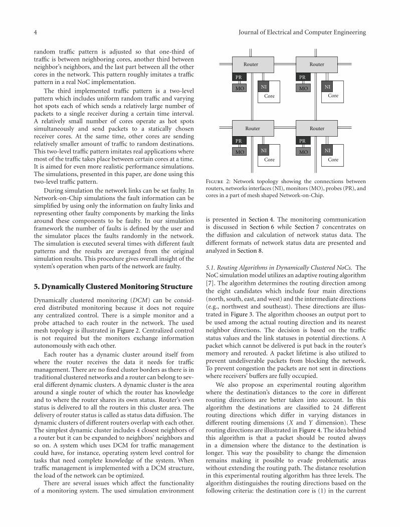
4 Journal of Electrical and Computer Engineering
random traffic pattern is adjusted so that one-third oftraffic is between neighboring cores, another third betweenneighbor’s neighbors, and the last part between all the othercores in the network. This pattern roughly imitates a trafficpattern in a real NoC implementation.
The third implemented traffic pattern is a two-levelpattern which includes uniform random traffic and varyinghot spots each of which sends a relatively large number ofpackets to a single receiver during a certain time interval.A relatively small number of cores operate as hot spotssimultaneously and send packets to a statically chosenreceiver cores. At the same time, other cores are sendingrelatively smaller amount of traffic to random destinations.This two-level traffic pattern imitates real applications wheremost of the traffic takes place between certain cores at a time.It is aimed for even more realistic performance simulations.The simulations, presented in this paper, are done using thistwo-level traffic pattern.
During simulation the network links can be set faulty. InNetwork-on-Chip simulations the fault information can besimplified by using only the information on faulty links andrepresenting other faulty components by marking the linksaround these components to be faulty. In our simulationframework the number of faults is defined by the user andthe simulator places the faults randomly in the network.The simulation is executed several times with different faultpatterns and the results are averaged from the originalsimulation results. This procedure gives overall insight of thesystem’s operation when parts of the network are faulty.
5. Dynamically Clustered Monitoring Structure
Dynamically clustered monitoring (DCM) can be consid-ered distributed monitoring because it does not requireany centralized control. There is a simple monitor and aprobe attached to each router in the network. The usedmesh topology is illustrated in Figure 2. Centralized controlis not required but the monitors exchange informationautonomously with each other.
Each router has a dynamic cluster around itself fromwhere the router receives the data it needs for trafficmanagement. There are no fixed cluster borders as there is intraditional clustered networks and a router can belong to sev-eral different dynamic clusters. A dynamic cluster is the areaaround a single router of which the router has knowledgeand to where the router shares its own status. Router’s ownstatus is delivered to all the routers in this cluster area. Thedelivery of router status is called as status data diffusion. Thedynamic clusters of different routers overlap with each other.The simplest dynamic cluster includes 4 closest neighbors ofa router but it can be expanded to neighbors’ neighbors andso on. A system which uses DCM for traffic managementcould have, for instance, operating system level control fortasks that need complete knowledge of the system. Whentraffic management is implemented with a DCM structure,the load of the network can be optimized.
There are several issues which affect the functionalityof a monitoring system. The used simulation environment
NI
PR
MOCoreCore
Core Core
NI
RouterRouter
Router
PR
MO
NI
PR
MO NI
PR
MO
Router
Figure 2: Network topology showing the connections betweenrouters, networks interfaces (NI), monitors (MO), probes (PR), andcores in a part of mesh shaped Network-on-Chip.
is presented in Section 4. The monitoring communicationis discussed in Section 6 while Section 7 concentrates onthe diffusion and calculation of network status data. Thedifferent formats of network status data are presented andanalyzed in Section 8.
5.1. Routing Algorithms in Dynamically Clustered NoCs. TheNoC simulation model utilizes an adaptive routing algorithm[7]. The algorithm determines the routing direction amongthe eight candidates which include four main directions(north, south, east, and west) and the intermediate directions(e.g., northwest and southeast). These directions are illus-trated in Figure 3. The algorithm chooses an output port tobe used among the actual routing direction and its nearestneighbor directions. The decision is based on the trafficstatus values and the link statuses in potential directions. Apacket which cannot be delivered is put back in the router’smemory and rerouted. A packet lifetime is also utilized toprevent undeliverable packets from blocking the network.To prevent congestion the packets are not sent in directionswhere receivers’ buffers are fully occupied.
We also propose an experimental routing algorithmwhere the destination’s distances to the core in differentrouting directions are better taken into account. In thisalgorithm the destinations are classified to 24 differentrouting directions which differ in varying distances indifferent routing dimensions (X and Y dimension). Theserouting directions are illustrated in Figure 4. The idea behindthis algorithm is that a packet should be routed alwaysin a dimension where the distance to the destination islonger. This way the possibility to change the dimensionremains making it possible to evade problematic areaswithout extending the routing path. The distance resolutionin this experimental routing algorithm has three levels. Thealgorithm distinguishes the routing directions based on thefollowing criteria: the destination core is (1) in the current

Journal of Electrical and Computer Engineering 5
R
N
E
S
W
NW NE
EN
ES
SESW
WS
WN
Figure 3: Routing directions. N: North, S: South, E: East, W: West,and R: Router.
−1
−1
Dis
tan
ce b
etw
een
cu
rren
t ro
ute
r an
d
Distance between current router and
Currentrouter
<−1
<−1
1
1
0
0
7
3 4 51
10986
11
15 16
21 22 23 24
12 13 14
191817
20
2
destination in X-direction
dest
inat
ion
in Y
-dir
ecti
on
>1
>1
Figure 4: Routing directions in our experimental routing algo-rithm.
row/column, (2) in the next row/column in some direction,or (3) further away. Hence, there are altogether 24 differentrouting directions. These routing directions enable extensiveclassification of different routing cases and that way each casecan be handled optimally.
In each of these 24 routing directions we have ranked thepossible output ports based on the destination and networkconditions. Every time a packet is routed the algorithmidentifies the routing direction and uses available trafficstatus and fault information to select the appropriate outputport.
6. Monitoring Algorithms and Communication
In the basic DCM structure the monitoring data is trans-ferred in packets using the actual data network. These packetsare called monitoring packets. The monitoring packetshave a higher priority in the routers so that they can betransferred even when there is congestion in the network.The monitoring packets are sent from a monitor to amonitor, but because the monitors are not directly connected
to each other, the packets are transferred via routers andlinks.
The router statuses in the DCM structure are representedwith two binary numbers, one for traffic status and anotherfor fault information. The status of a router is based on theoccupancy of the FIFO buffer where packets are waiting tobe routed forward. The faultiness of a single component canbe represented using a single bit while number of bits inthe traffic status values is related to the size of the FIFObuffer, required accuracy as well as the used additionalstatus data processing (see Section 7.1). The resolution of thetraffic status data is defined with status data granularity. Thegranularity defines the number of different values which canbe used to illustrate the level of traffic load. For instance,when the status granularity of a router is 4 there is 4 differentlevels of traffic (1: no or just a little traffic, 4: highly loadedand cannot receive new packets, 2-3: scaled linearly betweenthe edge values). The finer the granularity the better theaccuracy of the status values is.
In the DCM structure the monitors exchange their ownand their neighbors’ statuses with each other. Typicallymonitoring packets include fault statuses of nearby links andone or more traffic statuses of routers depending on the sizeof the monitoring cluster. The structure of a monitoringpacket payload in systems with monitoring cluster sizes 5and 13 is presented in Figure 5. The contents of a monitoringpacket payload are discussed in Section 7.
In centralized and clustered monitoring structures themonitoring packets are transferred in a network in the sameway as the data packets (see Section 2.1). The dynamicallyclustered approach simplifies the monitoring communica-tion because the routing of the monitoring packets is notneeded but substituted with a packet-type recognition. Everymonitor sends its status data and the neighbor status datait is forwarding to all its neighbors. The receiver recognizesthese packets as monitoring packets and does not send themforward. The transfer distance of a monitoring packet isalways one hop, from a router to its neighbor router. Thissimplicity of monitoring packet transferring combined withthe simple routing procedure of monitoring packets makesit possible to keep the latency overhead on tolerable level formost applications. The presented DCM structure is targetedfor applications without strict real-time constraints becausethe in-time delivery of packets cannot always be guaranteed.This is a trade-off of the improved fault tolerance.
A monitor stores the status data from received moni-toring packets to its memory and provides this informationforward to its own neighbors. This way the routers are ableto receive information not only from their neighbors butalso from the neighbors of their neighbors. In dynamicallyclustered monitoring structure the network status dataspreads over the network without centralized control andwithout routing related processing.
The update interval of a monitoring data denotes theconditions when a monitor sends an up-to-date monitoringpacket to its neighbors. In [16] we analyzed different updateintervals including static and dynamic intervals as well as ahybrid interval combining both of the previous ones. Thestatic interval sends a new packet after a certain time interval
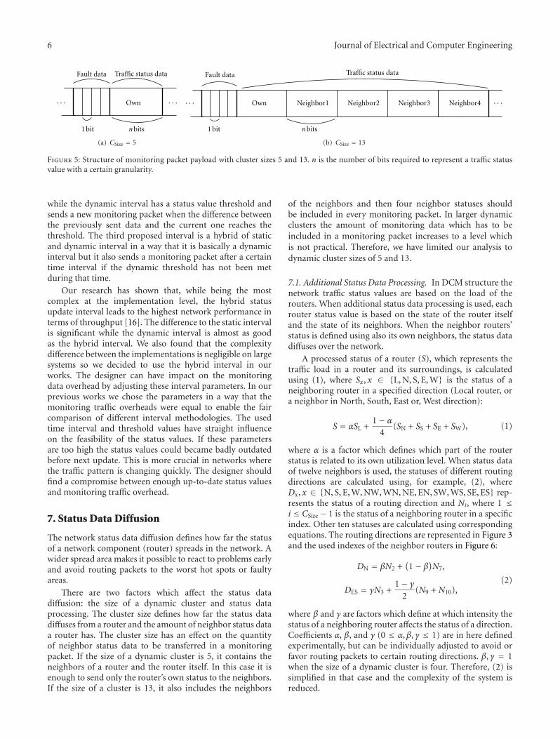
6 Journal of Electrical and Computer Engineering
Traffic status dataFault data
Own · · ·· · ·
1 bit n bits
(a) CSize = 5
Fault data Traffic status data
Own Neighbor1 Neighbor2 Neighbor3 Neighbor4· · · · · ·
1 bit n bits
(b) CSize = 13
Figure 5: Structure of monitoring packet payload with cluster sizes 5 and 13. n is the number of bits required to represent a traffic statusvalue with a certain granularity.
while the dynamic interval has a status value threshold andsends a new monitoring packet when the difference betweenthe previously sent data and the current one reaches thethreshold. The third proposed interval is a hybrid of staticand dynamic interval in a way that it is basically a dynamicinterval but it also sends a monitoring packet after a certaintime interval if the dynamic threshold has not been metduring that time.
Our research has shown that, while being the mostcomplex at the implementation level, the hybrid statusupdate interval leads to the highest network performance interms of throughput [16]. The difference to the static intervalis significant while the dynamic interval is almost as goodas the hybrid interval. We also found that the complexitydifference between the implementations is negligible on largesystems so we decided to use the hybrid interval in ourworks. The designer can have impact on the monitoringdata overhead by adjusting these interval parameters. In ourprevious works we chose the parameters in a way that themonitoring traffic overheads were equal to enable the faircomparison of different interval methodologies. The usedtime interval and threshold values have straight influenceon the feasibility of the status values. If these parametersare too high the status values could became badly outdatedbefore next update. This is more crucial in networks wherethe traffic pattern is changing quickly. The designer shouldfind a compromise between enough up-to-date status valuesand monitoring traffic overhead.
7. Status Data Diffusion
The network status data diffusion defines how far the statusof a network component (router) spreads in the network. Awider spread area makes it possible to react to problems earlyand avoid routing packets to the worst hot spots or faultyareas.
There are two factors which affect the status datadiffusion: the size of a dynamic cluster and status dataprocessing. The cluster size defines how far the status datadiffuses from a router and the amount of neighbor status dataa router has. The cluster size has an effect on the quantityof neighbor status data to be transferred in a monitoringpacket. If the size of a dynamic cluster is 5, it contains theneighbors of a router and the router itself. In this case it isenough to send only the router’s own status to the neighbors.If the size of a cluster is 13, it also includes the neighbors
of the neighbors and then four neighbor statuses shouldbe included in every monitoring packet. In larger dynamicclusters the amount of monitoring data which has to beincluded in a monitoring packet increases to a level whichis not practical. Therefore, we have limited our analysis todynamic cluster sizes of 5 and 13.
7.1. Additional Status Data Processing. In DCM structure thenetwork traffic status values are based on the load of therouters. When additional status data processing is used, eachrouter status value is based on the state of the router itselfand the state of its neighbors. When the neighbor routers’status is defined using also its own neighbors, the status datadiffuses over the network.
A processed status of a router (S), which represents thetraffic load in a router and its surroundings, is calculatedusing (1), where Sx, x ∈ {L, N, S, E, W} is the status of aneighboring router in a specified direction (Local router, ora neighbor in North, South, East or, West direction):
S = αSL +1− α
4(SN + SS + SE + SW), (1)
where α is a factor which defines which part of the routerstatus is related to its own utilization level. When status dataof twelve neighbors is used, the statuses of different routingdirections are calculated using, for example, (2), whereDx, x ∈ {N, S, E, W, NW, WN, NE, EN, SW, WS, SE, ES} rep-resents the status of a routing direction and Ni, where 1 ≤i ≤ CSize − 1 is the status of a neighboring router in a specificindex. Other ten statuses are calculated using correspondingequations. The routing directions are represented in Figure 3and the used indexes of the neighbor routers in Figure 6:
DN = βN2 +(1− β
)N7,
DES = γN3 +1− γ
2(N9 + N10),
(2)
where β and γ are factors which define at which intensity thestatus of a neighboring router affects the status of a direction.Coefficients α, β, and γ (0 ≤ α,β, γ ≤ 1) are in here definedexperimentally, but can be individually adjusted to avoid orfavor routing packets to certain routing directions. β, γ = 1when the size of a dynamic cluster is four. Therefore, (2) issimplified in that case and the complexity of the system isreduced.

Journal of Electrical and Computer Engineering 7
R
12
11
10
95
826
7
3
4
1
Figure 6: Indexes of the neighbor routers.
7.2. Diffusion Analysis. The analysis of network status diffu-sion is presented in Figures 7 and 8. The same simulation wasexecuted with two different dynamic cluster sizes withoutfaults and with 10% of network links being faulty. Theanalysis was not done with larger cluster sizes because theamount of transferred monitoring data then increases tointolerable level. The additional status data processing wasused in Figures 7(a) and 8(a). The processing coefficientswere experimentally chosen to obtain maximal throughputso that α = 0.5, β = 0.6, and γ = 0.6. When the additionalprocessing was not utilized (Figures 7(b) and 8(b)) the rawmonitored status data was used and the statuses of neighborrouters did not have influence on the router status values.
The differences in network performance appear when thethroughput has been fully or nearly saturated. The figuresshow that in a faultless network the performance differencesare notable. The proportional differences were measured atthe point where 60% (0.6 on the X-axle) of the maximumcapacity of packets were sent during a routing cycle. The60%point was chosen because it is clearly after the saturationpoint but still far from the maximum load.
All the following performance increment percentages arein proportion to the performance of an NoC with similarfault pattern, deterministic routing algorithm, and withoutnetwork monitoring. In a faultless network (see Figure 7) theperformance increase is 19% when status data processing isused, regardless of the monitoring cluster size. Surprisingly,when status data processing is turned off, the throughputincreases 23% and 21% in systems with monitoring clustersizes 5 and 13, respectively. Simulations were also executedin faulty networks where 10% of the links are set to unusablestate (see Figure 8). These links were randomly chosenand simulations were run with several different randomfault patterns. When status data processing is used, theperformance increases are 78% and 74% in networks withcluster sizes 5 and 13, respectively. Without status dataprocessing the corresponding values are 78% and 72%.
The analysis shows that DCM with small cluster sizeimproves network performance significantly. An especiallynotable feature is its ability to maintain the network through-put in a faulty network. Without network monitoring thethroughput decreases 41% when 10% of links becomefaulty. However, if the presented monitoring is used the
decrement is only 11%. Furthermore, the throughput in afaulty network with monitoring is 6% higher than it of afaultless network without monitoring.
A noteworthy observation is that a larger cluster size doesnot have positive impact on the performance but actuallyreduces it. This phenomenon can have multiple reasons.One reason for the inefficiency can be that too much dataprocessing leads to inaccurate status data and dissolves thedifferences between the statuses. Another reason could bethe latency in the status data propagation which makes itoutdated before it is utilized.
The influence of the additional status data processingis small or even nonexistent. In a faulty network there is avery small increase in the throughput. However, in faultlessnetwork the impact is even negative. For example, Figure 9shows the difference in throughput in faulty network withCSize = 5. As can be seen in this specific comparison thedifference is negligible.
The inefficiency of the status data processing may stemfrom the same factors as that of the large cluster size. Thedifferences between status values dissolve and are not ondisplay so that the routing algorithm could make rightdecisions.
8. Format of Network Status Data
The network status data is used to deliver the informationof the state of the network and it can be used to differentpurposes. When the main application is traffic managementthe data typically includes information concerning networkload and faults. Faults are simply denoted using binary valueswhich indicate if a component of the network is usable orfaulty. In more complex systems multilevel fault indicatorscould be considered. The network load is denoted usinga scale where different values represent different amountsof load on a network component. In our simulations thenetwork load representation is linear. Different scales can beconsidered in some specific applications.
8.1. Granularity of the Router Status Values. The status datagranularity defines the resolution of the status data values orhow many different values there are on the scale which is usedto represent the load on a network component. The smallestused value indicates that the load of a network componentis very low and the highest value represents high load ofthe component. Rest of the values indicate component loadlinearly between the extreme values. An example of thestatus data granularity was given in Section 6. In physicalimplementations the status data values are represented asbinary numbers which means that finer granularity requiresmore bits and that way increases the size of monitoringpacket payload. The status data granularity impacts onthe amount of the monitoring data to be transferred aswell as to the required computational resources in themonitoring components. The granularity should be chosenso that the required data transfer and status data processingresources are adequate in the framework of the current NoCimplementation.
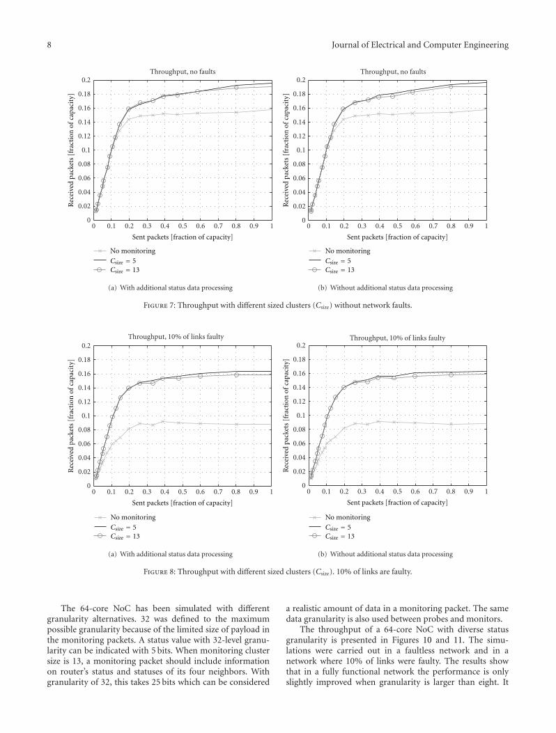
8 Journal of Electrical and Computer Engineering
0 0.1
0.1
0.2
0.2
0.3 0.4 0.5 0.6 0.7 0.8 0.9 10
0.02
0.04
0.06
0.08
0.12
0.14
0.16
0.18
Throughput, no faultsR
ecei
ved
pack
ets
[fra
ctio
n o
f ca
paci
ty]
Sent packets [fraction of capacity]
No monitoring
Csize = 5Csize = 13
(a) With additional status data processing
Throughput, no faults
0 0.1
0.1
0.2
0.2
0.3 0.4 0.5 0.6 0.7 0.8 0.9 10
0.02
0.04
0.06
0.08
0.12
0.14
0.16
0.18
Rec
eive
d pa
cket
s [f
ract
ion
of
capa
city
]
Sent packets [fraction of capacity]
No monitoring
Csize = 5Csize = 13
(b) Without additional status data processing
Figure 7: Throughput with different sized clusters (Csize) without network faults.
Throughput, 10% of links faulty
0 0.1
0.1
0.2
0.2
0.3 0.4 0.5 0.6 0.7 0.8 0.9 10
0.02
0.04
0.06
0.08
0.12
0.14
0.16
0.18
Rec
eive
d pa
cket
s [f
ract
ion
of
capa
city
]
Sent packets [fraction of capacity]
No monitoring
Csize = 5Csize = 13
(a) With additional status data processing
Throughput, 10% of links faulty
0 0.1
0.1
0.2
0.2
0.3 0.4 0.5 0.6 0.7 0.8 0.9 10
0.02
0.04
0.06
0.08
0.12
0.14
0.16
0.18
Rec
eive
d pa
cket
s [f
ract
ion
of
capa
city
]
Sent packets [fraction of capacity]
No monitoring
Csize = 5Csize = 13
(b) Without additional status data processing
Figure 8: Throughput with different sized clusters (Csize). 10% of links are faulty.
The 64-core NoC has been simulated with differentgranularity alternatives. 32 was defined to the maximumpossible granularity because of the limited size of payload inthe monitoring packets. A status value with 32-level granu-larity can be indicated with 5 bits. When monitoring clustersize is 13, a monitoring packet should include informationon router’s status and statuses of its four neighbors. Withgranularity of 32, this takes 25 bits which can be considered
a realistic amount of data in a monitoring packet. The samedata granularity is also used between probes and monitors.
The throughput of a 64-core NoC with diverse statusgranularity is presented in Figures 10 and 11. The simu-lations were carried out in a faultless network and in anetwork where 10% of links were faulty. The results showthat in a fully functional network the performance is onlyslightly improved when granularity is larger than eight. It

Journal of Electrical and Computer Engineering 9
0 0.1
0.1
0.2
0.2
0.3 0.4 0.5 0.6 0.7 0.8 0.9 10
0.02
0.04
0.06
0.08
0.12
0.14
0.16
0.18
Rec
eive
d pa
cket
s [f
ract
ion
of
capa
city
]
Sent packets [fraction of capacity]
Throughput, 10% of links faulty
With processingWithout processing
Figure 9: Throughput with and without processing. Csize = 5, 10%of links are faulty.
can be also noted that in faulty network the granularityshould be at least 16. In both cases 4-level granularity leads tosignificantly lower performance which means 7% decrementin the faultless and 4% in the faulty network compared withthe 16-level granularity. This supports the use of at least16-level granularity. The performance of system withoutmonitoring is illustrated as a reference.
8.2. Combining Router and Link Statuses. A method tosimplify monitoring status data is to combine traffic andfault information. In the original status data format (seeFigure 5) there is a binary number to represent the trafficload and a bit to indicate the resource faultiness. To decreasethe monitoring complexity and the size of monitoring datapayload, we analyzed two approaches where the monitoringdata is combined to hybrid forms. These two hybrid dataformats are presented below.
8.2.1. Hybrid Status Data Using Traffic Status Values. Trafficstatus values can be used to indicate faults by defining thatthe maximum status value does not only indicate high trafficload but also faulty resources. If there is a faulty componentin some direction, the traffic status value of that directionis set to its maximum value. In this case the payload of amonitoring packet (see Figure 5) is reduced by 4 bits becausethe fault values are not included. When this format is utilizedthe routing algorithm has to be configured to totally avoidthe routing directions with maximum traffic values.
8.2.2. Hybrid Status Data Using Fault Indicator Values. Themonitoring data is simplified even further when all the statusdata is combined to the boolean fault indicator values. In thisapproach, a routing direction is marked as faulty when thereis high traffic load. The status can be restored when the trafficload decreases. This way packets are not routed in highly
loaded directions. A drawback in this approach is the loss ofknowledge about differences between routing directions withlow and medium traffic load. Because the traffic status valuesare not used, the reduction of the monitoring packet payloadis n bits if CSize = 5 and 5n bits if CSize = 13.
The monitoring data combination approaches weresimulated with the NoC model, and the results are presentedin Figure 12. Obviously, in faultless network the traffic-status-based combination works similarly as separate data.When the traffic data is integrated into the fault statuses thedecrease in throughput is 8%. However, the performance isstill 12% better than without monitoring. In faulty networkseparated status data is notably the best solution. The traffic-data-based hybrid format causes 24% performance losswhich is even larger with the fault-data-based format, 40%.Nevertheless, these hybrid formats increase the performanceby 36% and 8%, correspondingly, compared to the systemwithout traffic monitoring.
The presented analysis leads to a resolution that bothmonitoring data classes are necessary in a system where faultsare a realistic threat. In less vital applications the hybridformats could be a good compromise.
9. Serial Monitor Communication
In the DCM structure the monitoring data is transferredin the same network which is used by the original datapackets. It is a straightforward solution which minimizesthe requirement of additional resources. However, a shared-resource structure is always at least somewhat intrusive andit consumes the network resources which otherwise could beused by the actual data packets.
An alternative solution to the intermonitor commu-nication is serial communication which is implementedwith dedicated channels. It can be realized with relativelysmall amount of additional resources. A drawback in serialcommunication is the increased transfer delay. However,because the serial communication resources are dedicated tothe monitoring communication there can be a nonstop statusupdate without paying attention to update intervals [16].
Serial monitor communication was simulated with theSystemC-based NoC simulation model. Throughput withdifferent status data granularities and serial communicationis presented in Figure 13. The serial transmitter operatesat the same clock frequency as the maximum frequencyof the monitoring packet transmitter. However, the latterrarely works on its maximum frequency because of the statusupdate interval conditions.
Essentially serial communication is slower than theearlier discussed parallel, packet-based communication, andthe theoretical delays of the serial communication areeven more increased when there is large amount of datato be transferred, for example, in systems with relativelylarge monitoring clusters. However, in contrast the serialcommunication is operating in dedicated communicationresources which can be used only to this purpose all thetime. This way the status values can be updated actually moreoften than when the monitoring packets are transferred in

10 Journal of Electrical and Computer Engineering
Throughput, no faults
4816
32No monitoring
0 0.1
0.1
0.2
0.2
0.3 0.4 0.5 0.6 0.7 0.8 0.9 10
0.02
0.04
0.06
0.08
0.12
0.14
0.16
0.18
Rec
eive
d pa
cket
s [f
ract
ion
of
capa
city
]
Sent packets [fraction of capacity]
(a) No faults
Throughput, 10% of links faulty
4816
32No monitoring
0 0.1
0.1
0.2
0.2
0.3 0.4 0.5 0.6 0.7 0.8 0.9 10
0.02
0.04
0.06
0.08
0.12
0.14
0.16
0.18
Rec
eive
d pa
cket
s [f
ract
ion
of
capa
city
]
Sent packets [fraction of capacity]
(b) 10% of links are faulty
Figure 10: Throughput with different traffic status granularity alternatives. CSize = 5 and data processing is enabled.
Throughput, no faults
4816
32No monitoring
0 0.1
0.1
0.2
0.2
0.3 0.4 0.5 0.6 0.7 0.8 0.9 10
0.02
0.04
0.06
0.08
0.12
0.14
0.16
0.18
Rec
eive
d pa
cket
s [f
ract
ion
of
capa
city
]
Sent packets [fraction of capacity]
(a) No faults
Throughput, 10% of links faulty
4816
32No monitoring
0 0.1
0.1
0.2
0.2
0.3 0.4 0.5 0.6 0.7 0.8 0.9 10
0.02
0.04
0.06
0.08
0.12
0.14
0.16
0.18
Rec
eive
d pa
cket
s [f
ract
ion
of
capa
city
]
Sent packets [fraction of capacity]
(b) 10% of links are faulty
Figure 11: Throughput with different traffic status granularity alternatives. CSize = 13 and data processing is enabled.
the shared resources. Somewhat surprisingly the system withCSize = 13 works well also for coarser status granularitieswhen serial communication is utilized. This is a result ofshorter traffic status update interval even though in thiscase the amount of serially transferred data is quite large.In this case the granularity of 4 clearly stands out. Possiblythe granularity of 4 is simply too rough to be used withthe data amount of a system with large monitoring clusters.Figure 13(a) shows that when serial communication and
small cluster size are used the performance differences aremore notable also between granularities 8, 16, and 32. Whenserial communication is used in system with CSize = 5 theperformance with granularity of 32 is 11% less than with cor-responding system using monitoring packets. Respectively,the performance of a system with serial communicationand granularity of 4 is 39% better than the performance ofsystem without monitoring. The corresponding percentagesfor system with CSize = 13 are 6% and 42%.

Journal of Electrical and Computer Engineering 11
Throughput, no faults
Separate dataHybrid data: traffic
Hybrid data: faultsNo monitoring
0 0.1
0.1
0.2
0.2
0.3 0.4 0.5 0.6 0.7 0.8 0.9 10
0.02
0.04
0.06
0.08
0.12
0.14
0.16
0.18
Rec
eive
d pa
cket
s [f
ract
ion
of
capa
city
]
Sent packets [fraction of capacity]
(a) No faults
Throughput, 10% of links faulty
Separate dataHybrid data: traffic
Hybrid data: faultsNo monitoring
0 0.1
0.1
0.2
0.2
0.3 0.4 0.5 0.6 0.7 0.8 0.9 10
0.02
0.04
0.06
0.08
0.12
0.14
0.16
0.18
Rec
eive
d pa
cket
s [f
ract
ion
of
capa
city
]
Sent packets [fraction of capacity]
(b) 10% of links are faulty
Figure 12: Throughput with separate traffic and fault data as well as with the hybrid formats. CSize = 5 and data processing is enabled.
Throughput, 10% of links faulty
4816
32No monitoringMonitoring packets
0 0.1
0.1
0.2
0.2
0.3 0.4 0.5 0.6 0.7 0.8 0.9 10
0.02
0.04
0.06
0.08
0.12
0.14
0.16
0.18
Rec
eive
d pa
cket
s [f
ract
ion
of
capa
city
]
Sent packets [fraction of capacity]
(a) CSize = 5
Throughput, 10% of links faulty
4816
32No monitoringMonitoring packets
0 0.1
0.1
0.2
0.2
0.3 0.4 0.5 0.6 0.7 0.8 0.9 10
0.02
0.04
0.06
0.08
0.12
0.14
0.16
0.18
Rec
eive
d pa
cket
s [f
ract
ion
of
capa
city
]
Sent packets [fraction of capacity]
(b) CSize = 13
Figure 13: Throughput with different granularity alternatives using serial communication. 10% of links are faulty and data processing isenabled.
The serial communication could be a useful optionwhen a designer wants to keep the communication resourcesof different applications separately. The serial approachguarantees that the monitoring communication does notdisturb the actual data which is transferred in the network. Itmay be possible to increase the clock frequency of the serialtransmitter from what was used in the presented analysis. Inthis case the performance differences should shrink.
10. Using Fewer Monitors
The DCM system is based on a structure where there is anidentical monitor attached to each router. These monitorsinclude both monitoring and probing components. Onepotential way to reduce monitoring structure complexityis to decrease the number of monitors systematically byremoving every nth monitor. In this approach there is a probe

12 Journal of Electrical and Computer Engineering
XX
X X
X
X
X
X XX
X
X
XXX
XX X
X
X
X
Every 3rd monitor removed
X
X
X
X
X
X
X
X
X
X
Every 6th monitor removed
Figure 14: Two patterns of removed monitors. Removed monitors are marked with X.
Throughput, no faults
ReferenceEvery 2nd removedEvery 3rd removed
Every 6th removedEvery 12th removedNo monitoring
0 0.1
0.1
0.2
0.2
0.3 0.4 0.5 0.6 0.7 0.8 0.9 10
0.02
0.04
0.06
0.08
0.12
0.14
0.16
0.18
Rec
eive
d pa
cket
s [f
ract
ion
of
capa
city
]
Sent packets [fraction of capacity]
(a) No faults
Throughput, 10% of links faulty
ReferenceEvery 2nd removedEvery 3rd removed
Every 6th removedEvery 12th removedNo monitoring
0 0.1
0.1
0.2
0.2
0.3 0.4 0.5 0.6 0.7 0.8 0.9 10
0.02
0.04
0.06
0.08
0.12
0.14
0.16
0.18
Rec
eive
d pa
cket
s [f
ract
ion
of
capa
city
]
Sent packets [fraction of capacity]
(b) 10% of links are faulty
Figure 15: Throughput with fewer monitors. Csize = 5 and data processing is enabled.
attached to every router but a monitor is attached only toa limited number of routers. This means that there is stillcomplete knowledge of the network state in the monitorsbecause there is probes attached to every router. Two monitorremoval patterns are illustrated in Figure 14. The monitorsreceive probed data, process it, and deliver it to the localrouter. The routers that do not have their own monitorshould utilize a deterministic routing algorithm becausethey do not have access to the probed status data from theneighboring routers. An adaptive algorithm is utilized inthe other routers [7]. The simplified deterministic routersforward packets based on a deterministic routing algorithm.In problematic traffic or fault cases, a simplified router couldroute packets randomly just directing them to some of itsneighbors. In any case the neighbors of a deterministic routerare adaptive routers which can route the packet forwardadaptively.
In addition to performance, the reduction of monitorsaffects the complexity of the NoC implementation. Routerswhich do not have their own monitoring component couldhave less complex routing logic which decreases the router
area. This is due to the deterministic routing algorithm whichsubstitutes the adaptive routing algorithm in the routerswhich do not have a monitoring component. However, theprobing components cannot be simplified because they havestill have to offer status data to other monitors.
This approach was analyzed using our SystemC-basedNoC simulation model and the results are presented inFigure 15. The simulation cases were chosen so that theunmonitored routers are placed as evenly as possible in thenetwork. This way we defined four simulation cases whereevery second, every third, every sixth, and every twelfthmonitor was removed from the network.
The figure shows that the removal of a monitor, evenif it is just every 12th, has notable influence on networkthroughput and the influence is even more remarkable whenthere are faults in the network. Removal of every secondmonitor causes 18% performance decrement in faultlessnetwork and 43% in the network with 10% of faulty links.In faultless network the performance is equal with theperformance of a system without traffic monitoring. Infaulty network there is 2% performance increase compared

Journal of Electrical and Computer Engineering 13
to the unmonitored system. If just every 12th monitor isremoved, the performance decreases by 3% and 10%, respec-tively.
The removal of monitors has positive impact to area andtraffic overheads caused by the monitoring system. However,the total area of the monitoring system is almost negligiblecompared to the area of a 64-core NoC. This way the removalof monitors cannot be justified with the reduced complexitywhen the performance decrement is as large as presentedhere. In application-specific NoCs it could be reasonable toremove monitors from areas where traffic is predictable sothat the resources can be sized properly during the designphase and adaptivity is not necessary. However, in our workthe focus is on homogeneous general-purpose NoCs so themonitors are placed evenly over the network.
11. Discussion and Conclusions
The dynamically clustered monitoring structure for fault-tolerant Networks-on-Chip has been presented and analyzedin this paper. Dynamically clustered monitoring does notrequire any centralized control. There is a simple monitorand a probe attached to each router in the network. Cen-tralized control is not required but the monitors exchangeinformation with each other. Each router has a dynamiccluster around itself from where a router collects the data itneeds for traffic management. The different features of thedynamically clustered monitoring structure were analyzedand their influence on the overall performance of the systemwere studied. Most of these presented features can be utilizedin different NoC implementations with various requirementsand limitations. However, due to nature of adaptive, shared-resource system, the presented DCM structure could not bethe best solution to systems with strict real-time require-ments.
In future works the analysis of individual cores androuters will be improved. In this phase, the NoC simulationmodel does not enable the analysis of specific senders andreceivers but concentrates only on overall performance. Thismakes it possible to analyze how different monitoring meth-ods and parameters affect performance from a component’spoint of view.
Performance of the DCM structure could be adjusted byusing different sized monitoring clusters in different areas inthe network. Areas with low traffic load may work at rea-sonable performance using very simple deterministic routingalgorithms. At the same time in the same system there couldbe performance critical areas with high traffic loads andtight quality of service requirements. It could be necessary touse larger monitoring clusters and adaptive routing on theseareas. Another useful feature could be on-fly reconfigurationof cluster size and the routing algorithm. Performance andenergy consumption of the communication resources couldbe optimized by using more complex mechanisms in thecritical areas of the network.
Our SystemC-based NoC simulation model has beenproved to be an efficient tool to analyze and simulate differentaspects in Networks-on-Chip. The model is reasonably easy
to configure for the analysis of different features. TheNoC simulation model was used to analyze monitoringalgorithms, monitoring data diffusion areas, format ofmonitoring data and communication as well as numberof monitors. The presented research shows that in mostcases simple monitoring algorithms and small monitoringcluster areas perform at least as well as more compleximplementations. In this paper the most complex structuresdid not cause significant improvements to performance.However, these structures and algorithms may be developedfurther in the future works. Another observation is thateven small adjustments in the system parameters can havesignificant influence to the overall performance. Thereforethe parameters should be chosen carefully while designinga complex DCM structure.
Acknowledgments
The authors would like to thank the Academy of Finland,the Nokia Foundation, and the Finnish Foundation forTechnology Promotion for financial support.
References
[1] W. J. Dally and B. Towles, “Route packets, not wires: on-chipinterconnection networks,” in Proceedings of the 38th DesignAutomation Conference, pp. 684–689, June 2001.
[2] L. Benini and G. De Micheli, “Networks on Chip: a newparadigm for systems on chip design,” in Proceedings of theDesign, Automation and Test in Europe (DATE ’02), pp. 418–419, 2002.
[3] C. Grecu, A. Ivanov, R. Saleh, and P. P. Pande, “Testingnetwork-on-chip communication fabrics,” IEEE Transactionson Computer-Aided Design of Integrated Circuits and Systems,vol. 26, no. 12, pp. 2201–2213, 2007.
[4] D. Bertozzi, L. Benini, and G. De Micheli, “Error con-trol schemes for on-chip communication links: the energy-reliability tradeoff,” IEEE Transactions on Computer-AidedDesign of Integrated Circuits and Systems, vol. 24, no. 6, pp.818–831, 2005.
[5] T. Lehtonen, D. Wolpert, P. Liljeberg, J. Plosila, and P.Ampadu, “Self-adaptive system for addressing permanenterrors in on-chip interconnects,” IEEE Transactions on VeryLarge Scale Integration Systems, vol. 18, no. 4, pp. 527–540,2010.
[6] V. Rantala, T. Lehtonen, P. Liljeberg, and J. Plosila, “Analysisof monitoring structures for network-on-chip—a distributedapproach,” IGI International Journal of Embedded and Real-Time Communication Systems, vol. 2, no. 1, pp. 49–67, 2011.
[7] W. J. Dally and B. Towles, Principles and Practices of Intercon-nection Networks, Morgan Kaufmann, 2004.
[8] V. Nollet, T. Marescaux, and D. Verkest, “Operating-systemcontrolled Network on Chip,” in Proceedings of the 41st DesignAutomation Conference, pp. 256–259, 2004.
[9] R. Mouhoub and O. Hammami, “NoC monitoring hardwaresupport for fast NoC design space exploration and potentialNoC partial dynamic reconfiguration,” in Proceedings of theInternational Symposium on Industrial Embedded Systems(IES ’06), pp. 1–10, October 2006.
[10] K. Goossens, J. Dielissen, and A. Radulescu, “Æthereal net-work on chip: concepts, architectures, and implementations,”
14 Journal of Electrical and Computer Engineering
IEEE Design and Test of Computers, vol. 22, no. 5, pp. 414–421,2005.
[11] C. Ciordas, K. Goossens, T. Basten, A. Radulescu, and A.Boon, “Transaction monitoring in networks on chip: the on-chip run-time perspective,” in Proceedings of the InternationalSymposium on Industrial Embedded Systems (IES ’06), pp. 1–10, October 2006.
[12] J. van den Brand, C. Ciordas, K. Goossens, and T. Bas-ten, “Congestion-controlled best-effort communication forNetworks-on-Chip,” in Proceedings of the Design, Automationand Test in Europe (DATE ’07), pp. 1–6, April 2007.
[13] M. Al Faruque, T. Ebi, and J. Henkel, “ROAdNoC: runtimeobservability for an adaptive Network on Chip architecture,”in Proceedings of the IEEE/ACM International Conference onComputer-Aided Design (ICCAD ’08), pp. 543–548, November2008.
[14] T. Marescaux, A. Rangevall, V. Nollet, A. Bartic, and H. Corpo-raal, “Distributed congestion control for packet switched Net-works on Chip,” in Proceedings of the International ConferenceParCo, pp. 761–768, 2005.
[15] P. Gratz, B. Grot, and S. Keckler, “Regional congestion aware-ness for load balance in networks-on-chip,” in Proceedings ofthe IEEE 14th International Symposium on High PerformanceComputer Architecture (HPCA ’08), pp. 203–214, February2008.
[16] V. Rantala, T. Lehtonen, P. Liljeberg, and J. Plosila, “Analysis ofstatus data update in dynamically clustered network-on-chipmonitoring,” in Proceedings of the 1st International Conferenceon Pervasive and Embedded Computing and CommunicationSystems (PECCS ’11), March 2011.

Hindawi Publishing CorporationJournal of Electrical and Computer EngineeringVolume 2012, Article ID 278735, 11 pagesdoi:10.1155/2012/278735
Research Article
A Hardware Design of Neuromolecular Network withEnhanced Evolvability: A Bioinspired Approach
Yo-Hsien Lin1 and Jong-Chen Chen2
1 Department of Information Management, Yuanpei University, 306 Yuanpei Street, Hsinchu 30015, Taiwan2 Department of Information Management, National Yunlin University of Science and Technology, 123 University Road,Section 3, Douliou, Yunlin 64002, Taiwan
Correspondence should be addressed to Jong-Chen Chen, [email protected]
Received 14 July 2011; Revised 30 August 2011; Accepted 30 August 2011
Academic Editor: Jiang Xu
Copyright © 2012 Y.-H. Lin and J.-C. Chen. This is an open access article distributed under the Creative Commons AttributionLicense, which permits unrestricted use, distribution, and reproduction in any medium, provided the original work is properlycited.
Silicon-based computer systems have powerful computational capability. However, they are easy to malfunction because of aslight program error. Organisms have better adaptability than computer systems in dealing with environmental changes or noise.A close structure-function relation inherent in biological structures is an important feature for providing great malleability toenvironmental changes. An evolvable neuromolecular hardware motivated by some biological evidence, which integrates inter-and intraneuronal information processing, was proposed. The hardware was further applied to the pattern-recognition domain.The circuit was tested with Quartus II system, a digital circuit simulation tool. The experimental result showed that the artificialneuromolecularware exhibited a close structure-function relationship, possessed several evolvability-enhancing features combinedto facilitate evolutionary learning, and was capable of functioning continuously in the face of noise.
1. Introduction
Effective programmability is an important feature inherentin computer systems, including software and hardware,which allows us to explore various problem domains. How-ever, most of computer systems are brittle in the sense that aslight modification of a system’s structure can inadvertentlychange its functions or cause it to malfunction [1]. Thisis because computer systems possess a mapping structurewith fitness landscapes consisting of isolated peaks thatare separated by wide, deep valleys. By contrast, organismspossess a mapping structure with fitness landscapes holdingsome degree of smoothness that a slight change in an organ-ism’s gene structure generally will not significantly alter itsfunctions. Finding feasible solutions within a reasonable timemay become much easier in a smooth landscape than in arugged landscape [2]. In biological systems, the smoothness(gradualism) property is naturally represented in the closestructure-function relationship.
In the early 1990s, some other researchers concentratedon applying evolutionary techniques to hardware design.
They attempted to use a reconfigurable hardware to con-tinually change the internal circuit structure until the desiredstructure appears. This field was called evolvable hardware(EHW). EHW brought an interdisciplinary integration. Onesuch idea is to combine the merits of biological sys-temsand computer systems together and hopefully create hard-ware with better adaptability. For example, Sipper andRonald [3] proposed an FPGA circuit to simulate the glob-albehaviour of a swarm of fireflies. Mange et al. [4] success-fully applied evolutionary techniques into the design of atimer (stopwatch) and a full watch (biowatch) with digitalcircuits. Higuchi and his colleagues [5, 6] worked on thedevelopment of a number of evolvable hardware chips forvarious applications, including an analog chip for cellularphones, a clock-timing chip for Gigahertz systems, a chipfor autonomous reconfiguration control, a data compressionchip, and a chip for controlling robotic hands. Murakawaet al. [7] applied evolutionary techniques to reconfigureneural network topology, de Garis [8, 9] developed anartificial brain that assembled a group of cellular automata-based neural net modules to control a robot, and Torresen
2 Journal of Electrical and Computer Engineering
[10] designed an evolutionary digital circuit to controlprosthetic hands.
Our goal is to provide the digital machine with arepresentation of the internal structure-function relationsof biological systems, to capture some of the dynamicmodes of the processing of these systems, and to incorporatelearning algorithms of the type used in natural systems.Redundancy, weak interactions, and compartmentalizationare three important features inherent in biological structuresthat facilitate evolutionary learning [1]. The proposed sys-tem (artificial neuro molecular system, ANM) is a plasticarchitecture with rich dynamics that combines these threefeatures into the system, in particular into the subneuronallevel of processing. We note that redundancy allows anorganism to absorb genetic changes and yet wait for othermutations to join together to make a significant changein its phenotypic traits. By virtue of redundancy, severalgenetic mutations do not have to occur simultaneously. Weakinteraction is the other indispensable feature for facilitatingevolution. When the interactions among the constitutedcomponents of a system are small, adding a componentinto (or removing it from) a system will not significantlyalter its outputs (or functions). This allows a system tostabilize its current state in responding to structural changesor environmental changes. Compartmentalization is anotherevolution-friendliness feature. It allows a system to block offdisturbance or noise in the environment.
2. Architecture of ANM
The ANM model was motivated from the molecular mecha-nisms inside real neurons. The model consists of two typesof neurons: cytoskeletal neurons and reference neurons.Cytoskeletal neurons have significant intraneuronal informa-tion processing that might directly or indirectly relate to theirfiring behavior. They combine, or integrate, input signals inspace and time to yield temporally patterned output signals.Reference neurons serve as pointers to other neurons in a waythat allows for interneuronal memory manipulation.
In this section, we introduce the intraneuronal archi-tecture that plays the role of integrating spatiotemporalsignals inside a neuron and the interneuronal architecturethat orchestrates groups of neurons for performing coherenttasks. We then explain the evolutionary learning algorithmused in this model.
2.1. Operation Hypotheses. The model is based on twohypotheses.
H1. There are some brain neurons in charge of the time-space information transition. This kind of neuron iscalled cytoskeletal neuron. Cytoskeletal neurons arebased on the operation hypothesis between the nervecell cytoskeletons and molecules, producing a time-space input signal and transducing it into a series oftime outputs [1, 11].
H2. There are some brain neurons in charge of memorycontrol and neuron group organization. This kind ofneuron is called reference neurons. The purpose of
reference neurons is to form a common-goal infor-mation processing group from cytoskeletal neurons.By the memory screening of reference neurons, eachworkgroup would have neurons of different internalstructures, thus being able to finish the group task[1, 11].
2.2. Intraneuronal Architecture. It has been firmly establishedby now that information processing inside a neuron issignificant. The objective of the present study is not toidentify the precise nature of these mechanisms, but rather tocapture the working hypothesis that the cytoskeleton servesas a signal integration system. Our model is restricted tothe membrane components. In the present implementation,the membrane of the cytoskeleton is abstracted as a macro-molecular network (a cytoskeletal network) comprising anumber of components capable of initiating, transmitting,and integrating cytoskeletal signals. Our assumption isthat an inter-neuronal signal impinging on the membraneof a neuron is converted to an intraneuronal signal (acytoskeletal signal) transmitting on the cytoskeleton. Thisprocess was called “transduction”; therefore, a cytoskeletalneuron could be considered a transducer with a specificstructure. Cytoskeletal neurons are platforms of messageprocessing, and they are inspired by the signal integrationand memory function of the cytoskeleton.
This research utilized 2D cellular automata (CA) [11–13]to conduct the experiment of cytoskeletal neurons, and thewraparound fashion links were adopted for the CA arrange-ment. A cytoskeleton has multiple molecule networks ofmicrotubules, microfilaments, and neurofilaments. In orderto simulate these networks, we defined three kinds of fibersto make a cytoskeleton type (C-type), and the fibers werenamed C1, C2, and C3. Each of the cytoskeletal elements willhave its own shape, thus forming the cytoskeletal moleculenetworks. The conformation of each cytoskeletal element isvariable; therefore, molecule-mass-like groups may possiblybe formed. Different types of cytoskeletal elements havedifferent signal transmission features. C1 has the strongestsignal bearing capacity, but it has the slowest transmissionspeed. C3 has the weakest signal bearing capacity, but it hasthe fastest speed. C2’s performance is between C1 and C3.The illustration of cytoskeletal neurons structure is shown inFigure 1. Each cytoskeletal neuron has its unique cytoskeletalfiber structure. The types of signal flows depend on the dif-ferent structures and different transmission characteristics.Some signal flow would execute the transduction tasks witha diffusion-like method, sometimes fast and sometimes slow.
When an external stimulus hits a cytoskeletal neuronmembrane, it will activate the readin enzyme at that location.The activation will cause a signal flow to transmit along theroute of the same cytoskeletal elements. For example, afterthe on-location (3, 2) readin received the external input, itwill transmit the signals to its eight neighbors that have thesame cytoskeletal element locations. The illustration showsthat it can transmit the signal to C2 at locations (2, 2) and(4, 2). Any cytoskeletal element that receives this kind ofsignal will do the same, thus forming the phenomenon of
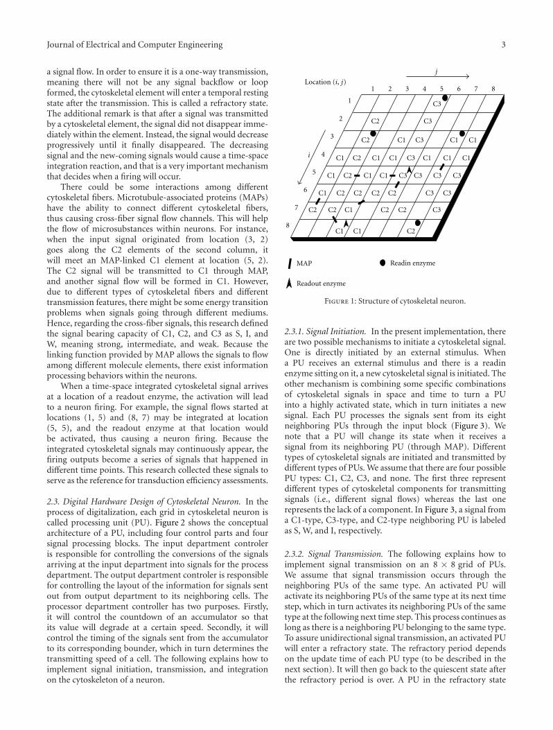
Journal of Electrical and Computer Engineering 3
a signal flow. In order to ensure it is a one-way transmission,meaning there will not be any signal backflow or loopformed, the cytoskeletal element will enter a temporal restingstate after the transmission. This is called a refractory state.The additional remark is that after a signal was transmittedby a cytoskeletal element, the signal did not disappear imme-diately within the element. Instead, the signal would decreaseprogressively until it finally disappeared. The decreasingsignal and the new-coming signals would cause a time-spaceintegration reaction, and that is a very important mechanismthat decides when a firing will occur.
There could be some interactions among differentcytoskeletal fibers. Microtubule-associated proteins (MAPs)have the ability to connect different cytoskeletal fibers,thus causing cross-fiber signal flow channels. This will helpthe flow of microsubstances within neurons. For instance,when the input signal originated from location (3, 2)goes along the C2 elements of the second column, itwill meet an MAP-linked C1 element at location (5, 2).The C2 signal will be transmitted to C1 through MAP,and another signal flow will be formed in C1. However,due to different types of cytoskeletal fibers and differenttransmission features, there might be some energy transitionproblems when signals going through different mediums.Hence, regarding the cross-fiber signals, this research definedthe signal bearing capacity of C1, C2, and C3 as S, I, andW, meaning strong, intermediate, and weak. Because thelinking function provided by MAP allows the signals to flowamong different molecule elements, there exist informationprocessing behaviors within the neurons.
When a time-space integrated cytoskeletal signal arrivesat a location of a readout enzyme, the activation will leadto a neuron firing. For example, the signal flows started atlocations (1, 5) and (8, 7) may be integrated at location(5, 5), and the readout enzyme at that location wouldbe activated, thus causing a neuron firing. Because theintegrated cytoskeletal signals may continuously appear, thefiring outputs become a series of signals that happened indifferent time points. This research collected these signals toserve as the reference for transduction efficiency assessments.
2.3. Digital Hardware Design of Cytoskeletal Neuron. In theprocess of digitalization, each grid in cytoskeletal neuron iscalled processing unit (PU). Figure 2 shows the conceptualarchitecture of a PU, including four control parts and foursignal processing blocks. The input department controleris responsible for controlling the conversions of the signalsarriving at the input department into signals for the processdepartment. The output department controler is responsiblefor controlling the layout of the information for signals sentout from output department to its neighboring cells. Theprocessor department controller has two purposes. Firstly,it will control the countdown of an accumulator so thatits value will degrade at a certain speed. Secondly, it willcontrol the timing of the signals sent from the accumulatorto its corresponding bounder, which in turn determines thetransmitting speed of a cell. The following explains how toimplement signal initiation, transmission, and integrationon the cytoskeleton of a neuron.
1
2
3
4
5
6
7
8
i
j
Location (i, j)
MAP
C2
C1
C3
C3
C3
C3
C3
C2
C2
C2
C2
C2
C1
C1
C2
C1
C1
C2
C1
C1
C1
C1
C1
C2 C2
C2 C2
C3
C1
C1
C1
C3
C3
C2
C1
C1
C3
C3
C3
1 2 3 4 5 6 7 8
C1
Readout enzyme
Readin enzyme
Figure 1: Structure of cytoskeletal neuron.
2.3.1. Signal Initiation. In the present implementation, thereare two possible mechanisms to initiate a cytoskeletal signal.One is directly initiated by an external stimulus. Whena PU receives an external stimulus and there is a readinenzyme sitting on it, a new cytoskeletal signal is initiated. Theother mechanism is combining some specific combinationsof cytoskeletal signals in space and time to turn a PUinto a highly activated state, which in turn initiates a newsignal. Each PU processes the signals sent from its eightneighboring PUs through the input block (Figure 3). Wenote that a PU will change its state when it receives asignal from its neighboring PU (through MAP). Differenttypes of cytoskeletal signals are initiated and transmitted bydifferent types of PUs. We assume that there are four possiblePU types: C1, C2, C3, and none. The first three representdifferent types of cytoskeletal components for transmittingsignals (i.e., different signal flows) whereas the last onerepresents the lack of a component. In Figure 3, a signal froma C1-type, C3-type, and C2-type neighboring PU is labeledas S, W, and I, respectively.
2.3.2. Signal Transmission. The following explains how toimplement signal transmission on an 8 × 8 grid of PUs.We assume that signal transmission occurs through theneighboring PUs of the same type. An activated PU willactivate its neighboring PUs of the same type at its next timestep, which in turn activates its neighboring PUs of the sametype at the following next time step. This process continues aslong as there is a neighboring PU belonging to the same type.To assure unidirectional signal transmission, an activated PUwill enter a refractory state. The refractory period dependson the update time of each PU type (to be described in thenext section). It will then go back to the quiescent state afterthe refractory period is over. A PU in the refractory state

4 Journal of Electrical and Computer Engineering
Processing unit (PU)
NeighboringPUs
NeighboringPUs
Firing
MAPcontrol
Readoutcontrol
PU-typecontrol
Input block
Integrationblock
Interruptblock
Output block
Switch
Readincontrol1
23
45
67
8
6 71 2 3 4 5 8
Figure 2: Conceptual architecture of a PU. The input block is illustrated in Figure 3, the interrupt block in Figure 4(a), the output block inFigure 4(b), and the integration block in Figure 6.
I
S
W
I
S
W
I
S
W
m1m2
m8
MAPcontrol
Input block
Interrupt block
NeighboringPUs
Switch
Integrationblock
PU1
PU8
···
···
···
···
···
···
···
···
Figure 3: Conceptual architecture of the input block.
will ignore any stimuli during the refractory period. Thiswould prevent a signal from bouncing repeatedly betweentwo neighboring PUs. We note that the refractory time is animportant parameter that may affect the performance in thepresent hardware design. That is, different output is possiblewhen length of the refractory time of each type is varied. Butour goal at this stage is to fulfill the function that a PU servesas a signal integrator that combines different signals in spaceand time (the detail will be described in the next section).That is, the refractory time is fixed and will not be involvedin the evolutionary change. In the present implementation,we have not performed a systematical experiment along thisline. But it would be interesting to perform the experimentin the near future.
A switch controlled by the interrupt block is used toregulate the signal flow from the input block to the integra-tion block (Figure 4(a)). The timing of control is through theoutput block (Figure 4(b)). When a PU is in the state of being
ready to take any signals from its neighboring PUs, its outputblock will turn on the switch (through the interrupt block)by sending it a high-voltage signal. This indicates that anysignal from its neighboring PU is allowed to change the stateof a PU. However, the switch will be turned off if a PU iseither in the state of processing a neighboring signal or in therefractory state.
2.3.3. Signal Integration. As mentioned earlier, there arethree types of PUs for transmitting signals. Our implementa-tion of signal integration is that, to fire a neuron, it requiresat least two different types of signals to rendezvous at a PUwithin a short period of time. In other words, a PU servesas a signal integrator that combines different signals in spaceand time. To capture this feature, two hypotheses are used.The first is that different PU types have different transmissionspeeds. The second hypothesis is that an activated PU caninfluence the state of its neighboring PU through MAP

Journal of Electrical and Computer Engineering 5
I
S
W
I
S
W
OnAction
CLK
Switch
Interrupter
Interrupt block
Inputblock
Outputblock
20
21
0123
Integrationblock
PU-type
m10
m9 2 × 4decoder
C1C2C3
control
(a)
I
S
W
Integrationblock
m10
m9
OutIn
Delayer
D
Interruptblock
Output block
NeighboringPUs
C2C3
PU-type
20
21
0123
CLK
C1Flip-flop
Q Dcontrol
decoder2 × 4
(b)
Figure 4: The interrupt block (a) and the output block (b).
I
S
S, I
W
S, I ,W
W W
I
s1
q3
q2
q0 q1 q4
(a) C1- type PU
S, I
W
S, I ,W
S, I ,W
q2
q0
q1 q3, q4
(b) C2- type PU
S, I ,W
S, I ,W
S, I ,W
q3, q4
q0
q2
q1
(c) C3- type PU
Figure 5: Transition rules of a PU. S, I, and W indicate a signal from a highly activated C1-, C2-, and C3-type PU, respectively. For example,if C1-type PU in the state q0 receives an I signal it will enter the moderately activated state q2. If it receives a W signal it will enter the moreactivated state q3. For example, a C1-type PU in the state q0 will enter the less active state q1 when it receives a signal from a neighboringC3-type PU (i.e., signal W). We note that if a PU does not receive a stimulus before its next update time, it will go into state q1 if it was instate q2, or enter state q0 if it was in q1.
linking them together. That is, the latter will make a statetransition when it receives a signal from the former.
We assume that a PU has six possible states: quiescent(q0), active with increasing levels of activity (q1, q2, q3,and q4), and refractory (qr). Certainly, the complexity ofintraneuronal dynamics will be greater when a larger numberof PU states are allowed. Correspondingly, it will increase thecomplexity of the hardware design. We note that six statesare sufficient for present use. The following describes thetransition rules of each PU. A PU in the highly active state(q 3 or q4) will return to the refractory state (qr) at its nextupdate time, and then go into the quiescent state (q0) at thefollowing next update time. The next state for a less activePU (q0, q1, or q2) depends on the sum of all stimuli receivedfrom its active neighboring PUs (Figure 5). If a PU does notreceive a stimulus before its next update time, it will go intostate q1 if it was in state q2, or enter state q0 if it was in q1.
In the present implementation, a signal traveling alongC1-type PUs has the slowest speed, but also has the greatestdegree of influence on the other two PU types. In contrast,a signal traveling along C3-type PUs has the fastest speed,
but also has the least degree of influence on the other twoPU types. The speed and the degree of influence of a C2-typesignal are between those of a C1- and C3-type signal. We notethat the degrees of influence between two different PU typesare asymmetrical. For example, a C1-type PU in the state q0
will enter the less active state q1 when it receives a signal froma neighboring C3-type PU (i.e., signal W). By contrast, a C3-type PU in the state q0 will enter a highly activated state q3 if itreceives a signal from a neighboring C1-type PU (i.e., signalS). Roughly speaking, the signal with the greatest degree ofinfluence serves as the major signal flow in a neuron whilethe other two types of signals provide modulating effects.
The integration block is the major component of theANM design that integrates signals transmitting in space andtime (Figure 6). The comparator is responsible for processingeither an external signal linked with its application domainor a cytoskeletal signal from its neighboring PU. For eachexternal signal sent to a PU, we assume that the latter willdirectly go into a highly active state (q3) if there is a readinenzyme sitting at the same site. This allows the initiationof a new cytoskeletal signal. As to a signal sending from its

6 Journal of Electrical and Computer Engineering
IS
WIS
W
(>3)
CLK
20
21
22
23
Comparator
Data
CLK
3-bitadder
CLK
Regulator
CLK
Divider
CLK
4-bit downcounter
CLK
Multiplier
/3 /2 /1
PU-type control
Inputcontrol
Firing
Outputblock
Integration block
(=3)
(>3)
Outputcontrol
Input
block
m12m11
20
21
22
20
21
22
20
21
22
20
21
22
20
21
22
202122
202122
202122
23
202122
23
202122
23
202122
×3×2×1
C1 C2 C3 C1 C2 C3 C1 C2 C3
(max output=5)
Figure 6: Conceptual architecture of the integration block.
neighboring PU, the comparator determines the state changeof a PU. The adder serves as a recorder that keeps a recordof a PU’s present state. Different numbers represent differentstates. Different types of PUs have different transmissionspeeds. The present implementation is that the ratio oftransmission speeds of C1-, C2-, and C3-type PUs is 1 : 2 : 3.To comply with the transmission speeds, the ratio of stateupdate times of C1-, C2-, and C3-type PUs is 3 : 2 : 1.Our hardware implementation of speed control comprisesa multiplier, a downcounter, and a divider. The multipliermagnifies a signal sent from the regulator and generates anoutput for the downcounter. The degree of magnification isdetermined by its update time. For each clock, the down-counter decreases by one. The divider restores the magnifiedsignal in the downcounter back to its original range.
All of the digital circuit modules were design with Verilogusing Quartus II software, a digital circuit design tool de-veloped by the Altera Corporation (San Jose, CA). The finaldesign of circuits were downloaded into an FPGA devicewhich produced by the Altera Corporation.
2.4. Interneuronal Architecture-Orchestral Learning. The ref-erence neuron scheme is basically a Hebbian model, inwhich the connection between two neurons is strengthenedwhen they are active simultaneously. This model also hasa hierarchical control feature. With this feature, referenceneurons are capable of assembling cytoskeletal neurons intogroups for performing specific tasks. Orchestration is anadaptive process mediated by varying neurons in the as-sembly which selects appropriate combinations of neuronsto complete specific tasks. Currently, cytoskeletal neuronsare divided into a number of comparable subnets. By com-parable subnets, we mean that neurons in these subnets
are similar in terms of their inter-neuronal connections andintraneuronal structures. Neurons in different subnets thathave similar inter-neuronal connections and intraneuronalstructures are grouped into a bundle.
Two levels of reference neurons are used to manipulatethese bundles of neuron. The two levels form hierarchicalcontrol architecture (Figure 7). The first is referred to asthe low-level reference neurons that directly control thebundles of cytoskeletal neurons. Each of these controls aspecific bundle (we note that only the bundles activated bythe reference neurons are allowed to perform informationprocessing). The second level is referred to as the high-levelreference neurons that play the role of grouping the low-levelreference neurons. The activation of a high-level referenceneuron will fire all of the low-level reference neurons that itcontrols, which in turn will activate some of these bundles ofcytoskeletal neurons (i.e., neurons in different subnets thathave similar intraneuronal structures). For example, whenR2
fires, it will fire r1 and r32, which in turn causes E1 and E32 ineach subnet to fire.
The connections among low-level reference neurons andcytoskeletal neurons are fixed. However, the connectionsbetween high-level reference neuron and low-level referenceneuron layers are subjected to change during evolutionarylearning. The above process is called orchestral learning.
2.5. Evolutionary Learning. Processing units are responsiblefor transmitting and integrating cytoskeletal signals. Evolu-tion at the level of PU configurations is implemented bycopying (with mutation) the PU configurations of neurons inthe best-performing subnets to those of comparable neuronsin the lesser-performing subnets. Variation is implementedby varying the PU configurations during the copy procedure.
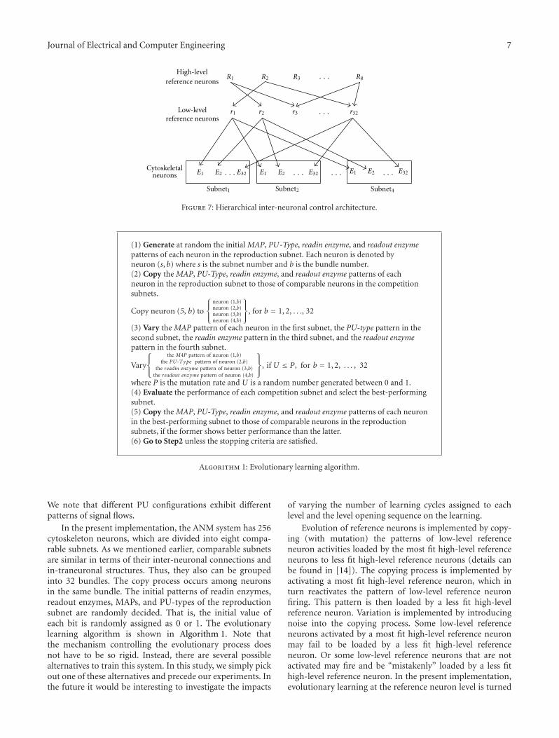
Journal of Electrical and Computer Engineering 7
R1 R2 R3 R8
r1 r2 r3 r32
High-levelreference neurons · · ·
Cytoskeletalneurons
Low-levelreference neurons
E1 E2 E32
· · ·
· · · E1 E2 E32· · · E1 E2 E32· · ·· · ·Subnet1 Subnet2 Subnet4
Figure 7: Hierarchical inter-neuronal control architecture.
(1) Generate at random the initial MAP, PU-Type, readin enzyme, and readout enzymepatterns of each neuron in the reproduction subnet. Each neuron is denoted byneuron (s, b) where s is the subnet number and b is the bundle number.(2) Copy the MAP, PU-Type, readin enzyme, and readout enzyme patterns of eachneuron in the reproduction subnet to those of comparable neurons in the competitionsubnets.
Copy neuron (5, b) to
⎧⎨⎩
neuron (1,b)neuron (2,b)neuron (3,b)neuron (4,b)
⎫⎬⎭, for b = 1, 2, . . ., 32
(3) Vary the MAP pattern of each neuron in the first subnet, the PU-type pattern in thesecond subnet, the readin enzyme pattern in the third subnet, and the readout enzymepattern in the fourth subnet.
Vary
⎧⎨⎩
the M4P pattern of neuron (1,b)the PU-Type pattern of neuron (2,b)
the readin enzyme pattern of neuron (3,b)the readout enzyme pattern of neuron (4,b)
⎫⎬⎭, if U ≤ P, for b = 1, 2, . . . , 32
where P is the mutation rate and U is a random number generated between 0 and 1.(4) Evaluate the performance of each competition subnet and select the best-performingsubnet.(5) Copy the MAP, PU-Type, readin enzyme, and readout enzyme patterns of each neuronin the best-performing subnet to those of comparable neurons in the reproductionsubnets, if the former shows better performance than the latter.(6) Go to Step2 unless the stopping criteria are satisfied.
Algorithm 1: Evolutionary learning algorithm.
We note that different PU configurations exhibit differentpatterns of signal flows.
In the present implementation, the ANM system has 256cytoskeleton neurons, which are divided into eight compa-rable subnets. As we mentioned earlier, comparable subnetsare similar in terms of their inter-neuronal connections andin-traneuronal structures. Thus, they also can be groupedinto 32 bundles. The copy process occurs among neuronsin the same bundle. The initial patterns of readin enzymes,readout enzymes, MAPs, and PU-types of the reproductionsubnet are randomly decided. That is, the initial value ofeach bit is randomly assigned as 0 or 1. The evolutionarylearning algorithm is shown in Algorithm 1. Note thatthe mechanism controlling the evolutionary process doesnot have to be so rigid. Instead, there are several possiblealternatives to train this system. In this study, we simply pickout one of these alternatives and precede our experiments. Inthe future it would be interesting to investigate the impacts
of varying the number of learning cycles assigned to eachlevel and the level opening sequence on the learning.
Evolution of reference neurons is implemented by copy-ing (with mutation) the patterns of low-level referenceneuron activities loaded by the most fit high-level referenceneurons to less fit high-level reference neurons (details canbe found in [14]). The copying process is implemented byactivating a most fit high-level reference neuron, which inturn reactivates the pattern of low-level reference neuronfiring. This pattern is then loaded by a less fit high-levelreference neuron. Variation is implemented by introducingnoise into the copying process. Some low-level referenceneurons activated by a most fit high-level reference neuronmay fail to be loaded by a less fit high-level referenceneuron. Or some low-level reference neurons that are notactivated may fire and be “mistakenly” loaded by a less fithigh-level reference neuron. In the present implementation,evolutionary learning at the reference neuron level is turned

8 Journal of Electrical and Computer Engineering
off, as we have not yet implemented it on digital circuits.The realization of the evolutionary learning on digital circuitat the reference neuron level is definitely a must-do step,but undoubtedly a complicated job. But in the presentimplementation, we are not ready to fulfill the design andprefer to focus our study on the internal dynamics, instead ofthe interneuronal dynamics.
3. Input/Output Interface andApplication Domain
We applied the chip to the IRIS dataset, one of the bestknown datasets found in the pattern recognition literature.The dataset was taken from the machine learning repositoryat the University of California, Irvine. The dataset contains3 classes (Iris Setosa, Iris Versicolour, Iris Virginica) of 50instances each, where each class refers to a type of iris plant.One class is linearly separable from the other two; the latter
are not linearly separable from each other. There are fourparameters in each instance: sepal length, sepal width, petallength, and petal width.
The initial connections between these 4 parameters andcytoskeletal neurons were randomly decided, but subjectto change as learning proceeded. Through evolutionarylearning, each cytoskeletal neuron was trained to be aspecific input-output pattern transducer. That is, each ofthese neurons became responsible for processing only a smallsubset of stimuli generated from these 4 parameters. Weused five bits to encode each of these 4 parameters. Intotal, there were 20 bits required to encode all of them. Foreach parameter, the minimal and maximal values of these150 instances were determined (to be denoted by MIN andMAX, resp.), and the difference between these two values wasdivided by 5 (to be denoted by INCR). The transformation ofeach actual parameter value (to be denoted by ACTUAL) intothe corresponding 5-bit pattern was shown to be
00001, if MIN ≤ ACTUAL < (MIN + INCR)
00010, if (MIN + INCR) ≤ ACTUAL < (MIN + INCR× 2)
00100, if (MIN + INCR× 2) ≤ ACTUAL < (MIN + INCR× 3)
01000, if (MIN + INCR× 3) ≤ ACTUAL < (MIN + INCR× 4)
10000, if (MIN + INCR× 4) ≤ ACTUAL ≤ MAX.
(1)
Each bit corresponded to a specific pattern of stimuli forcytoskeletal neurons. All cytoskeletal neurons that had con-nections with a specific bit would receive the same pattern ofstimuli simultaneously. When a readin enzyme received anexternal stimulus, a cytoskeletal signal was initiated. It wasrandomly decided in the beginning and subject to changeduring the course of learning as to which readin enzymesof a neuron would receive the stimuli from a parameter. Foreach instance, all stimuli were sent to cytoskeletal neuronssimultaneously. In other words, all cytoskeletal signals wereinitiated at the same time. The cytoskeleton integrated thesesignals in space and time. For each instance, the class of thefirst firing cytoskeletal neuron was assigned as its output.Cytoskeletal neurons were equally divided into three classes,corresponding to these three different groups of instances.For each instance, we defined that the chip made a correctresponse when the class of the first firing neuron was inaccordance with the group shown in the dataset (Figure 8).The ANM design was tested with each of these 150 instancesin sequence. The greater the number of correct responsesmade by the chip, the higher its fitness.
4. Experimental Results4.1. Evolvability. The proposed hardware architecture incor-porated several parameters PU, MAP, readin, and readout(denoted as P, M, I, and O, resp.) that allowed us to turn themon or off independently for evolutionary learning. We firststudy the manner in which problem-solving capability (or
evolvability) depended on each level of parameter changes.And then we investigated the effects of increasing thenumber of evolutionary learning parameters (levels) openedfor evolution. For each case of parameter changes (to bedescribed later), five runs were performed. For each run,100 out of these 150 instances in the IRIS set were selectedat random as the training set whereas the remaining 50instances were grouped as the testing set. All the resultsreported below were the average differentiation rates of fiveruns. We first trained the chip for 1200 cycles (at which pointlearning appeared to slow down significantly). Then, the chipafter learning for 1200 cycles was tested with the testing set.The IRIS dataset includes 150 instances. In the evolvabilityexperiment, the dataset were performed for five runs. Foreach run, the IRIS dataset was randomly divided into twoparts: training set and testing set. The training set includes100 instances and testing set 50 instances. We trained thechip for 1,200 cycles per run. It takes about 30 seconds tocomplete a learning cycle. The total running time of thisexperiment takes about 50 hours (30 s ∗ 1200 cycles ∗ 5runs). When compared with BP neural network and SVM,the time needed to perform the experiment with our systemis much longer than we expect. This is because the wholesystem has been simulated in a computer that simulationhas to be performed in a step-by-step manner. When thehardware design has been totally realized with a real digitalchip, it might take only microsec-onds to accomplish theassigned tasks.

Journal of Electrical and Computer Engineering 9
Cytoskeletalneurons
I1
Sepallength
I5
E1
E2
E30
An instance
firingneuron
A pattern
EkSamegroup
Yes
Correctclassification
Fourparameters
No
Wrong
I16
Pedalwidth
I20
Plant type
···
···
···
···
classification
first
(E1–10: Iris Setosa; E11–20: Iris Versicolour; E21–30: Iris Virginica)
Figure 8: Interface of the ANM design with the IRIS dataset.
To investigate the significance of each parameter, we firstallowed only one parameter to change during the courseof learning whereas evolution at the other three levels wasturned off. In total, there were four experiments performed.Among these four parameters, the chip after learning whenonly readin enzymes were allowed to evolve alone achievedthe highest recognition rate (i.e., 91.6%), when only PU typeswere allowed the second highest (i.e., 90.0%), when onlyMAPs were allowed the third highest (i.e., 84.4%), and whenonly readout enzymes were allowed the lowest rate (83.6%).This provided us some preliminary information about whichlevels of parameter changes might be friendlier to evolutionthan others.
The following experiment was to study the manner inwhich problem-solving capability (or evolvability) dependedon different combinations of parameter changes. We firstincreased the number of parameter changes to two (i.e.,two parameters were allowed to evolve simultaneously).There were six combinations of two parameter changes.As shown in Figure 9, the chip after learning when twolevels were allowed to evolve simultaneously achieved higherrecognition rates than when only one level was allowed toevolve alone. For example, the recognition rate was higherwhen PUs and MAPs were allowed to evolve simultaneouslythan when either PUs or MAPs were allowed to evolve alone.This implied that each level of parameter changes more orless contributed in facilitating evolutionary learning, andthat synergy occurred among different levels of learning.We then performed the experiment that allowed threeparameters to evolve at the same time. There were fourpossible combinations when three parameters were allowedto evolve simultaneously. The chip after learning when PMI(PU, MAP, and readin enzyme) were allowed to change at thesame time achieved the best recognition rate (94.0%) amongthese four possible combinations (note that a parameterthat was not opened for evolutionary changes will be heldconstant during the course of learning). The implication wasthat synergies among different levels of evolution became
more important as more levels of parameter changes wereallowed; implying that learning at one level opened upopportunities for another. However, it did not necessarilymean that learning with more levels of evolutionary changescould always achieve effective performance, in particularwhen the limitation of learning time was imposed. This wasbecause the power of a multilevel system was not attained bysimply summing up the contributions of each constitutingelement together, but by developing the synergy that mightoccur among the interactions of different levels. Learningwith more levels of evolutionary changes would enhancethe repertoire of the system, but did not guarantee thateffective learning could be achieved with a limited amountof time. When we looked into what levels (operators) ofevolution contributed to the learning progress and howthe interactions occurring between different levels exertedcontrol over the tempo of evolution, the result showed thateach operator more or less contributed to learning progress,and that learning proceeded in an alternate manner. Thatis, synergies percolated through different combinations ofevolutionary learning operators, implying that learning atone level opened up opportunities for another. We notedthat synergy was more likely to occur when a comparativelysmall number of parameter changes was involved. However,synergy occurred only in a selective manner when moreparameter changes were involved.
4.2. Comparison with Other Neural Models. For comparisonwe applied SVM and BP to the same training and testing sets.As above, five runs were performed. In the former model theaverage differentiation rates of the training and testing setswere 95.6% and 91.9%, respectively, while in the latter were96.7% and 91.7, respectively. The above result suggested thatthe chip had performance comparable to either BP or SVM(Table 1).
4.3. Noise Tolerance. This experiment was to test the capabil-ity of the ANM design after substantial learning in tolerating

10 Journal of Electrical and Computer Engineering
P M I O
PM MI PI MO PO IO
PU MAP Readin Readout
PMI MIO PMO PIO
PMIO
90% 84.4% 91.6% 83.6%
91.6% 92.4% 91.6% 91.6% 90.8% 90.8%
94% 92% 89.2% 91.2%
92%
Figure 9: Learning performance of each learning mode.
Table 1: Average differentiation rates of different models with theIris dataset.
Model Training Testing
BP neural network 96.7% 91.7%
Support vector machine 95.6% 91.9%
ANM 94.8% 94.0%
noise. Through gradually increasing the degree of noise, weobserved the input/output relationship of the ANM design.For each test, we kept the system’s structure unchanged butvaried the pattern of signals sent to cytoskeletal neurons.If the system’s outputs changed gradually with the extentof the increase in pattern variations, this in part supportedthat the system’s structure embraced some degree of noisetolerance capability. The ANM design trained for 1,200 cycleswas used.
In the following, we first tested the system with spatialnoise imposed on the training patterns. To generate a testset, we made a copy of the training set, but altered somebits during the copy process (changing a bit into “1” if it was“0” and into “0” if it was “1”). Five levels of variations wereimposed during the copy process: 5%, 10%, 15%, 20%, and25%. For example, at the 5% level of variations, we meanthat each bit has a 5% possibility of being altered. For eachlevel of variations, ten test sets were generated. The totalclock difference (TCD) value is the measure pointer indicatesthe difference of firing time in the circuit. The TCD valueincreased slightly as we imposed a 5% level of variations onthe patterns. Even when we increased the variation level to25%, the system still demonstrated acceptable results. TheTCD value was increased from 38 to 310 at the 5% level
Table 2: Effect of increasing the degree of noise on the rate of theTCD value growth.
Level of variations imposed 5.0% 10.0%
Rate of the TCD value increased 5.7% 11.1%
of variation (i.e., increased 272), to 569 at the 10% levelof variation (i.e., increased 531), to 633 at the 15% levelof variation (i.e., increased 625), to 626 at the 20% level ofvariation (i.e., increased 588), and to 1030 at the 25% level ofvariation (i.e., increased 992). If we divided the incrementsby the TCD value before learning (i.e., 4781), the rate of theTCD values increased gradually as we augmented the noiselevels (Table 2). This implied that the system had good noisetolerance capability in dealing with spatial noise.
5. Conclusions
When a system is running in the real world, it is inevitableto be confronted with noise generated either from theenvironment or the system itself. When noise is made onlytemporarily, structural changes of a system may not benecessary (i.e., a system may ignore this noise). By contrast, asystem is required to alter its structure in responding to thisnoise if it leads to a permanent change in the environment.In such a case, a system has to learn in a moving landscapewhen environmental change occurs from time to time. Twomain results are obtained in the noise tolerance experiment.One is that learning is more difficult in a noisy environmentthan in a noiseless environment, and that the system is ableto learn continuously when noise is made in a temporarymanner. The other result is that the system demonstrates

Journal of Electrical and Computer Engineering 11
a close structure/function relation. We note that noiseoccurring at different levels of the cytoskeletal structure hasdifferent degree of influence on its outputs. As we graduallymodify the structure, its outputs change accordingly. On theother hand, we examine the system’s outputs by graduallyimposing noise in space and time on its input patterns.The output changes gradually (i.e., proportionally) as thedegree of noise is increased. An interesting result is thatits system’s output does not necessarily change accordinglyas we increase the degree of noise generated in time. Notethat delaying a signal may alter a neuron’s firing activity.However, this may not be true when several signals aredelayed simultaneously as these signals may integrate at alater time (undoubtedly, this will delay its firing timing). Theabove results demonstrate that this system has good noisetolerance capability in dealing with spatiotemporal changesin its inputs, implying that it possesses an adaptive surfacethat facilitates evolutionary learning. With this feature, theANM design can be applied to various real-world problems.We note that the ability to separate patterns is clearly aprerequisite for pattern recognition. However, it is equallyimportant to recognize a family of patterns that are slightlyvaried in space and time. If a system is trained on a particulartraining set, any ability that it has to respond correctlyto noise induced variations in this set will be a form ofgeneralization. The manner of generalization depends onits integrative dynamics (i.e., the flow of signals in thecytoskeleton). This is directly or indirectly influenced by aneuron’s PU configuration. Generally speaking, the inputpatterns recognized by a neuron with internal dynamics willbe generalized in a more selective way than simple thresholdneurons.
Acknowledgment
This paper was supported in part by the R.O.C. NationalScience Council (Grant NSC 98-2221-E-224-018-MY3).
References
[1] M. Conrad, “Bootstrapping on the adaptive landscape,” BioS-ystems, vol. 11, no. 2-3, pp. 167–182, 1979.
[2] M. Conrad, “The geometry of evolution,” BioSystems, vol. 24,no. 1, pp. 61–81, 1990.
[3] M. Sipper and E. M. A. Ronald, “A new species of hardware,”IEEE Spectrum, vol. 37, no. 3, pp. 59–64, 2000.
[4] D. Mange, M. Sipper, A. Stauffer, and G. Tempesti, “Towardrobust integrated circuits: the embryonics approach,” Proceed-ings of the IEEE, vol. 88, no. 4, pp. 516–540, 2000.
[5] T. Higuchi, M. Iwata, D. Keymeulen et al., “Real-world ap-plications of analog and digital evolvable hardware,” IEEETransactions on Evolutionary Computation, vol. 3, no. 3, pp.220–234, 1999.
[6] T. Higuchi and N. Kajihara, “Evolvable hardware chips for in-dustrial applications,” Communications of the ACM, vol. 42,no. 4, pp. 60–66, 1999.
[7] M. Murakawa, S. Yoshizawa, I. Kajitani et al., “The GRD chip:genetic reconfiguration of DSPs for neural network process-ing,” IEEE Transactions on Computers, vol. 48, no. 6, pp. 628–639, 1999.
[8] H. de Garis, “An artificial brain ATR’s CAM-Brain Projectaims to build/evolve an artificial brain with a million neuralnet modules inside a trillion cell Cellular Automata Machine,”New Generation Computing, vol. 12, no. 2, pp. 215–221, 1994.
[9] H. de Garis, “Review of proceedings of the first NASA/Dodworkshop on evolvable hardware,” IEEE Transactions on Ev-olutionary Computation, vol. 3, no. 4, pp. 304–306, 1999.
[10] J. Torresen, “A divide-and-conquer approach to evolvablehardware,” in Proceedings of the 2th International Conferenceon Evolvable Systems: From Biology to Hardware, vol. 1478of Lecture Notes in Computer Science, pp. 57–65, Lausanne,Switzerland, 1998.
[11] M. Conrad, R. R. Kampfner, K. G. Kirby et al., “Towards an ar-tificial brain,” BioSystems, vol. 23, no. 2-3, pp. 175–218, 1989.
[12] J. C. Chen and M. Conrad, “A multilevel neuromolecular ar-chitecture that uses the extradimensional bypass principle tofacilitate evolutionary learning,” Physica D, vol. 75, no. 1–3,pp. 417–437, 1994.
[13] S. Rasmussen, H. Karampurwala, R. Vaidyanath, K. S. Jensen,and S. Hameroff, “Computational connectionism within neu-rons: a model of cytoskeletal automata subserving neural net-works,” Physica D, vol. 42, no. 1–3, pp. 428–449, 1990.
[14] I. Baradavka and T. Kalganova, “Assembling strategies inextrinsic evolvable hardware with bidirectional incrementalevolution,” Lecture Notes in Computer Science (including sub-series Lecture Notes in Artificial Intelligence and Lecture Notesin Bioinformatics), vol. 2610, pp. 276–285, 2003.
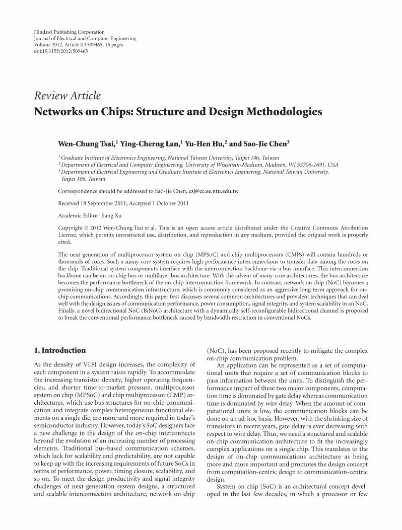
Hindawi Publishing CorporationJournal of Electrical and Computer EngineeringVolume 2012, Article ID 509465, 15 pagesdoi:10.1155/2012/509465
Review Article
Networks on Chips: Structure and Design Methodologies
Wen-Chung Tsai,1 Ying-Cherng Lan,1 Yu-Hen Hu,2 and Sao-Jie Chen3
1 Graduate Institute of Electronics Engineering, National Taiwan University, Taipei 106, Taiwan2 Department of Electrical and Computer Engineering, University of Wisconsin-Madison, Madison, WI 53706-1691, USA3 Department of Electrical Engineering and Graduate Institute of Electronics Enginering, National Taiwan University,Taipei 106, Taiwan
Correspondence should be addressed to Sao-Jie Chen, [email protected]
Received 18 September 2011; Accepted 1 October 2011
Academic Editor: Jiang Xu
Copyright © 2012 Wen-Chung Tsai et al. This is an open access article distributed under the Creative Commons AttributionLicense, which permits unrestricted use, distribution, and reproduction in any medium, provided the original work is properlycited.
The next generation of multiprocessor system on chip (MPSoC) and chip multiprocessors (CMPs) will contain hundreds orthousands of cores. Such a many-core system requires high-performance interconnections to transfer data among the cores onthe chip. Traditional system components interface with the interconnection backbone via a bus interface. This interconnectionbackbone can be an on-chip bus or multilayer bus architecture. With the advent of many-core architectures, the bus architecturebecomes the performance bottleneck of the on-chip interconnection framework. In contrast, network on chip (NoC) becomes apromising on-chip communication infrastructure, which is commonly considered as an aggressive long-term approach for on-chip communications. Accordingly, this paper first discusses several common architectures and prevalent techniques that can dealwell with the design issues of communication performance, power consumption, signal integrity, and system scalability in an NoC.Finally, a novel bidirectional NoC (BiNoC) architecture with a dynamically self-reconfigurable bidirectional channel is proposedto break the conventional performance bottleneck caused by bandwidth restriction in conventional NoCs.
1. Introduction
As the density of VLSI design increases, the complexity ofeach component in a system raises rapidly. To accommodatethe increasing transistor density, higher operating frequen-cies, and shorter time-to-market pressure, multiprocessorsystem on chip (MPSoC) and chip multiprocessor (CMP) ar-chitectures, which use bus structures for on-chip communi-cation and integrate complex heterogeneous functional ele-ments on a single die, are more and more required in today’ssemiconductor industry. However, today’s SoC designers facea new challenge in the design of the on-chip interconnectsbeyond the evolution of an increasing number of processingelements. Traditional bus-based communication schemes,which lack for scalability and predictability, are not capableto keep up with the increasing requirements of future SoCs interms of performance, power, timing closure, scalability, andso on. To meet the design productivity and signal integritychallenges of next-generation system designs, a structuredand scalable interconnection architecture, network on chip
(NoC), has been proposed recently to mitigate the complexon-chip communication problem.
An application can be represented as a set of computa-tional units that require a set of communication blocks topass information between the units. To distinguish the per-formance impact of these two major components, computa-tion time is dominated by gate delay whereas communicationtime is dominated by wire delay. When the amount of com-putational units is low, the communication blocks can bedone on an ad-hoc basis. However, with the shrinking size oftransistors in recent years, gate delay is ever decreasing withrespect to wire delay. Thus, we need a structured and scalableon-chip communication architecture to fit the increasinglycomplex applications on a single chip. This translates to thedesign of on-chip communications architecture as beingmore and more important and promotes the design conceptfrom computation-centric design to communication-centricdesign.
System on chip (SoC) is an architectural concept devel-oped in the last few decades, in which a processor or few

2 Journal of Electrical and Computer Engineering
processors along with memory and an associated set of pe-ripherals connected by busses are all implemented on a singlechip. According to the Moore’s law, the trend toward many-core processing chips is now a well established one. Power-efficient processors combined with hardware accelerators arethe preferred choice for most designers to deliver the besttradeoff between performance and power consumption,since computational power increases exponentially accord-ing to the calculation of dynamic power dissipation [1].Therefore, this trend dictates spreading the application tasksinto multiple processing elements where (1) each processingelement can be individually turned on or off, thereby savingpower, (2) each processing element can run at its own opti-mized supply voltage and frequency, (3) it is easier to achieveload balance among processor cores and to distribute heatacross the die, and (4) it can potentially produce lower dietemperatures and improve reliability and leakage. However,while ad-hoc methods of selecting few blocks may workbased on a designer’s experience, this may not work as to-day’s MPSoC and CMP designs which becomes more andmore complex. Consequently, SoC design nowadays needstechniques which can provide an efficient method of ena-bling a chip to compute complex applications and to fit area-wise on a single chip according to today’s technology trends.
A communication scheme is composed of an intercon-nection backbone, physical interfaces, and layered protocolswhich make the on-chip communication take place amongcomponents on a MP-SoC or CMP. As the design complex-ity scales up, intrachip communication requirements are be-coming crucial. Data-intensive systems such as multimediadevices, mobile installations, and multiprocessor platformsneed a flexible and scalable interconnection scheme to handlea huge amount of data transactions on chip. Customarily,dedicated point-to-point wires are adopted as sets of appli-cation-specific global on-chip links that connect the top-levelmodules. However, as wire density and length grow with thesystem complexity, the communication architecture basedon point-to-point wires becomes no more feasible due toits poor scalability and reusability. Specifically, as signals arecarried by the global wires across a chip, these metal wirestypically do not scale in length with technology. Propagationdelay, power dissipation, and reliability will be the seriousissues of global wires in deep submicron VLSI technology.According to [2], as silicon technologies advance to 50 nmand beyond, global wires will take 6 to 10 cycles to propagate,which will then far outweigh gate delays and make cross-chiplong wire timing difficult to meet. Keeping track of the statusin all elements and managing the global communicationamong top-level modules by a centralized way are no longerfeasible. Therefore, reusable on-chip bus interconnect tem-plates such as ARM’s AMBA [3] and IBM’s CoreConnect [4]are commonly used in current MP-SoC amd CMP designs,such that the modules can share the same group of intercon-nection wires in a bus-based communication architecture.
However, on-chip bus allows only one communicationtransaction at a time according to the arbitration result; thus,the average communication bandwidth of each processing el-ement is in inverse proportion to the total number of IP coresin a system. This character makes a bus-based architecture
inherently not scalable for a complex system in today’sMP-SoC and CMP designs. Implementing multiple on-chipbuses in a hierarchical architecture or in a separated mannermay alleviate this scalability constraint, but it requires ap-plication-specific grouping of processing elements and de-sign of different communication protocols to meet the appli-cation requirements. Furthermore, whenever a new applica-tion needs to be designed for, or a new set of peripheralsneeds to be added, a chip designed with only simple buseswill lack means of efficiently determining feasibility, not tomention optimality [5]. In addition, attempts to guaranteequality of service (QoS) for system performance will be amanually intensive task. Therefore, bus-based design needsto be exchanged with a method that is flexible, scalable, andreusable.
Since the latest process technology allows for more proc-essors and more cores to be placed on a single chip, theemerging MP-SoC and CMP architectures, which demandhigh throughput, low latency, and reliable global communi-cation services, cannot be met by current dedicated bus-based on-chip communication infrastructure. Trying toachieve such designs with a bus structure could be problem-atic for a number of reasons including timing closure, per-formance issues, and scalability. Specifically, as the featuresize of modern silicon devices shrinks below 50 nanometers,global interconnection delays constrain attainable processingspeed. Device parameter variations further complicate thetiming and reliability issues. A paradigm shift focusing oncommunication-centric design, rather than computation-centric design, seems to be the most promising approach toaddress these communication crises [6–11]. Consequently,in the past few years, a new methodology called network onchip has been introduced as a means of solving these issuesby introducing a structured and scalable communicationarchitecture.
In the sequel, Section 2 will introduce the NoC architec-ture and its function layers. In Section 3, we will discuss theNoC design methodologies. Then, a bidirectional network-on-chip (BiNoC) architecture will be given in Section 4.Finally, conclusion will be drawn in Section 5.
2. Network-on-Chip Architecture andFunction Layers
Network on chip is the term used to describe an architecturethat has maintained readily designable solutions in face ofcommunication-centric trends. In this section, we will brieflyreview some concepts on the design of an NoC communi-cation system. Moreover, the NoC function can be classifiedinto several layers, which will be introduced sequentially.
2.1. Network-on-Chip Architecture. A typical NoC architec-ture consists of multiple segments of wires and routers asshown in Figure 1. In a tiled, city-block style of NoC layout,the wires and routers are configured much like street grids ofa city, while the clients (e.g., logic processor cores) are placedon city blocks separated by wires. A network interface (NI)module transforms data packets generated from the client

Journal of Electrical and Computer Engineering 3
IP IP IP
IPIPIP
IP IP IP
NI NI
NI
NI
NINI
NI NI NI
NI
R
R
R R
R
RRR
R R
Network interface
Router
Source
Destination
Figure 1: Typical NoC architecture in a mesh topology.
logic (processor cores) into fixed-length flow-control digits(flits). The flits associated with a data packet consist of aheader (or head) flit, a tail flit, and a number of body flits inbetween. This array of flits will be routed toward the intendeddestination in a hop-by-hop manner from one router to itsneighboring router.
In a city-block style NoC, each router has five inputports and five output ports corresponding to the north, east,south, and west directions as well as the local processingelement (PE). Each port will connect to another port on theneighboring router via a set of physical interconnect wires(channels). The router’s function is to route flits enteringfrom each input port to an appropriate output port and thentoward the final destinations. To realize this function, arouter is equipped with an input buffer for each input port, a5 × 5 crossbar switch to redirect traffic to the desired outputport and necessary control logic to ensure correctness ofrouting results as shown in Figure 2.
Usually, for each data packet, the corresponding head flitspecifies its intended destination. After examining the headflit, the router control logic will determine which output di-rection to route all the subsequent (body and tail) flits associ-ated with this data packet according to the routing algorithmapplied.
2.2. Network-on-Chip Function Layers. The NoC functioncan be classified into several layers: application, transport,network, data link, and physical layers. An NoC routershould contain both software and hardware implementationsto support functions of the layers.
2.2.1. Application Layer. At the application layer, target ap-plications will be broken down into a set of computation andcommunication tasks such that the performance factors likeenergy and speed can be optimized. Placement of cores on anNoC has to be optimized to reduce the amount of total com-munication or energy but at the same time recognizing thelimitations of any one particular link. The task mapping andcommunication scheduling problem is an instance of a con-strained quadratic assignment problem which was knownto be NP-hard [12]. Given a target application described asa set of concurrent tasks with an NoC architecture, the funda-mental questions to answer are (1) how to topologically placethe selected set of cores onto the processing elements of thenetwork and (2) how to take into consideration the complexeffects of network condition, which may change dynamicallyduring task execution, such that the metrics of interest areoptimized [13]. To get the best tradeoff between power andperformance, application mapping and scheduling should beconsidered with several kinds of architecture parameters.
2.2.2. Transport Layer. To prevent buffer overflow and toavoid traffic congestion, some management schemes shouldbe applied to guide the transport of packets in an NoC. Thetransport layer addresses the congestion and flow control is-sues [14]. Key performance metrics of an NoC include lowpacket delivery latency and high-throughput rate, and thesemetrics are critically impacted by network congestions caus-ed by resource contentions. Accordingly, contention resolu-tion is a key to avoid network congestions [14]. One of themost crucial issues for the contention resolution is, under apremise of a deadlock- and livelock-free routing algorithm,to enhance the utilization efficiency of available network re-sources in order to come up with a better communicationperformance.
2.2.3. Network Layer. Network topology or interconnect ar-chitecture is an important issue in this layer, which deter-mines how the resources of network are connected, thus,refers to the static arrangement of channels and nodes in aninterconnection network. Irregular forms of topologies canbe derived by mixing different forms of communicationarchitectures in a hierarchical, hybrid, or asymmetric way byclustering partition, which may offer more connectivity andcustomizability at the cost of complexity and area. In addi-tion, optimization of a topology, which affects the connectiv-ity of the routers and the distance of any one core to the other,is difficult. Furthermore, the tradeoff between generality andcustomization that, respectively, facilitate scalability and per-formance is important. As future designs become more com-plex, the non-recurring costs of architecting and manufac-turing a chip will become more and more expensive. A ho-mogenous NoC is one where the cores and routers are all thesame, while a heterogeneous NoC selects individual coresfrom an IP library and may have its communication archi-tecture customized to suit the needs of an application. SinceNoC designs must be flexible enough to cover a certain rangeof applications, most of the state-of-the-art NoC designs usea mesh or torus topology because of its performance benefits

4 Journal of Electrical and Computer Engineering
West
West
Network
inte
rface
Controllogic
ControllogicContro
llo
gic
Con
trol
logi
cCon
trol
logi
c
East
input port
input port
input port
inpu
tp
ort
East
output port
outp
ut
port
inpu
tpo
rt
outp
ut
port
output port
output port
Nor
th
Nor
thSo
uth
Sou
th
Register
Register
Reg
iste
r
Reg
iste
r
Regist
er
Local
Local
Figure 2: Typical NoC router architecture.
and high degree of scalability for two-dimensional systems,yet it may not achieve the best performance for a single ap-plication [15, 16].
In addition, the network layer also needs to deal with therouting data between processing elements. First, packetizingalgorithms deal with the decomposition of a message intopackets at source nodes and their assembly at destinationnodes. Then, the transmission of packets can be executed bythe choice of routing algorithms based on different networktopologies [6]. Routing algorithm determines the path strat-egy of a packet from its source node to the destination node.Determining packet routes and resolving conflicts betweenpackets when the same route is requested, with respect to im-proving on-chip communication performance, are two of theimportant responsibilities of a router.
Conventional design of a router consists of circuit-switched fabrics and an arbitration controller. In each arbi-tration decision, more than one path can be constructed bythe crossroad switch as long as no contention exists betweenthese paths. For most existing switch designs, virtual-channelflow-control-based router design, which provides better flex-ibility and channel utilization with smaller buffer size, is awell-known technique from the domain of multiprocessornetworks [17–24].
2.2.4. Data Link and Physical Layers. The main purpose ofdata-link layer protocols is to increase the reliability of thelink up to a minimum required level, under the assumption
that the physical layer by itself is not sufficiently reliable [14].The emphasis on physical layer is focused on signal driversand receivers, as well as design technologies for resorting andpipelining signals on wiring. In addition, as technologyadvanced to ultradeep submicron (DSM), smaller voltageswings and shrinking feature size translate to decreased noisemargin, which cause the on-chip interconnects less immuneto noise and increase the chances of nondeterminism in thetransmission of data over wires (transient fault) [2, 25–28].Electrical noise due to crosstalk, electromagnetic interference(EMI), and radiation-induced charge injection will likelyproduce timing error and data errors and make reliable on-chip interconnect hard to achieve.
Error control schemes and utilization of the physicallinks to achieve reliability are the main concern of these lay-ers. First, a credible fault model must be developed. Then,an error control scheme that is low power, low area, highbandwidth, and low latency must be designed. In NoC de-sign, packet-based data transmission is an efficient way todeal with data errors because the effect of errors is containedby packet boundaries that can be recovered on a packet-by-packet basis.
3. Network-on-Chip Design Methodologies
This section discusses several prevalent NoC design method-ologies, such as flow control, routing, arbitration, quality ofservice, reliability, and task scheduling.

Journal of Electrical and Computer Engineering 5
Inpu
tpo
rtre
g
Switchallocator Output port
(N, S, W, PE)(N, S, W, PE)
Crossbar
Routingcomputation
Input buffer
channel req
Ou
tpu
tpo
rtre
g
Routing computation Switch allocation Switch traversal
Input port
Figure 3: Typical router design based on wormhole flow control.
3.1. Flow-Control Mechanism. The performance of NoCcommunication architecture is dictated by its flow-controlmechanism. Adding buffers to networks significantly im-proves the efficiency of a flow-control mechanism since abuffer can decouple the allocation of adjacent channels.Without a buffer, the two channels must be allocated to apacket (or flits) during consecutive cycles, or the packet mustbe dropped or misrouted [6]. More specifically, with bufferedflow control, when a packet arrives at a router, it must firstoccupy some resources, such as channel bandwidth and buff-er capacity, depending on the flow-control methodology.Each router must juggle among multiple input data streamsfrom multiple input ports and route them to appropriateoutput ports with the highest efficiency.
Buffered flow-control methods can be classified into pack-et-buffer flow control and flit-buffer flow control based ontheir granularity of buffer allocation and channel bandwidthallocation [6]. Since allocating resources in unit of flit canachieve more storage utilization efficiency than that in unitof packet. Two types of flit-buffer flow-control architecturesare commonly used in NoC: the wormhole flow control andthe virtual-channel flow control.
3.1.1. Packet-Buffer Flow Control. Packet-buffer flow-controlallocates network resources in a packet-by-packet basis. Ex-amples are store-and-forward flow control and virtual-cut-through flow control. In store-and-forward method, eachnode must ensure that it has already received and stored anentire packet before forwarding it to the downstream node.While the virtual-cut-through scheme can forward a packetas long as there is enough buffer space to receive a packet atthe downstream node. As a result, virtual cut through intro-duces lower communication delay than store and forwarddoes. However, packet-buffer flow control needs larger sizeof buffer space in one node because of its inefficient use ofbuffer storage. In addition, allocating channels in units ofpackets will increase contention latency.
3.1.2. Wormhole Flow-Control-Based Router. Wormhole flowcontrol improves performance through a finer granularity ofmessage allocation at flit level instead of packet level. This
technique allows more efficient use of buffer than the packet-buffer flow-control mechanism since the buffer size in eachrouter can be reduced significantly [29, 30]. A typical three-stage pipelined NoC router architecture based on wormholeflow control is shown in Figure 3. Every input port hasa FIFO-based input buffer, which can be seen as a singlevirtual channel used to hold blocked flits. To facilitate worm-hole flow-control-based routing [6], the routing computation(RC) module will send a channel request signal to the switchallocator (SA) for data in each input buffer. If the down-stream buffer at a neighboring router has vacant space, SAwill allocate the channel and route the data flits through thecrossbar switch toward the designated downstream router atthe switch traversal (ST) stage.
However, wormhole flow-control-based switching tech-nique saves buffer size at the expense of throughput since thechannel is owned by a packet, but buffers are allocated on aflit-by-flit basis. As such, an idle packet may continue blocka channel even when another packet is ready to use the samechannel, leading to inefficient resource utilization. This is thewell-known head of line (HoL) blocking problem. Therefore,virtual-channel flow-control-based router architecture wasproposed to reduce blocking effect and to improve networklatency.
3.1.3. Virtual-Channel Flow-Control-Based Router. Virtual-channel flow control assigns multiple virtual paths, each withits own associated buffer queue, to the same physical chan-nel; thus, it increases throughput by up to 40% over worm-hole flow control and helps to avoid possible deadlock prob-lems [19, 31, 32]. A virtual channel flow-control router archi-tecture as shown in Figure 4 can be seen as a remedy to theshortcoming of the wormhole flow-control scheme. By mul-tiplexing multiple virtual-channels into the same input buff-er, an idle packet will no longer block other packets that areready to be routed using the shared physical channel. In atypical virtual-channel flow-control-based router, the flitsare routed via a four-stage pipeline: routing computation,virtual-channel allocation, switch allocator, and switch traver-sal.
One incoming flit that arrives at a router is first writtento an appropriate input virtual-channel queue and waits to
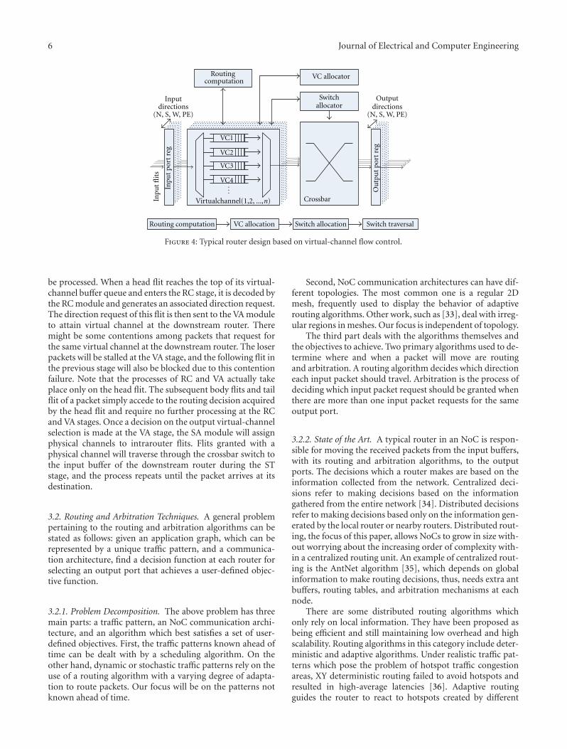
6 Journal of Electrical and Computer Engineering
VC allocator
Inputdirections directions
VC1
VC2
VC3
VC4
VC allocation Switch allocation Switch traversal
Routingcomputation
Switchallocator
Routing computation
Inpu
tpo
rtre
g
Ou
tpu
tpo
rtre
g
Output
(N, S, W, PE)(N, S, W, PE)
Inpu
tfl
its
Crossbar
...
Virtualchannel(1,2, ...,n)
Figure 4: Typical router design based on virtual-channel flow control.
be processed. When a head flit reaches the top of its virtual-channel buffer queue and enters the RC stage, it is decoded bythe RC module and generates an associated direction request.The direction request of this flit is then sent to the VA moduleto attain virtual channel at the downstream router. Theremight be some contentions among packets that request forthe same virtual channel at the downstream router. The loserpackets will be stalled at the VA stage, and the following flit inthe previous stage will also be blocked due to this contentionfailure. Note that the processes of RC and VA actually takeplace only on the head flit. The subsequent body flits and tailflit of a packet simply accede to the routing decision acquiredby the head flit and require no further processing at the RCand VA stages. Once a decision on the output virtual-channelselection is made at the VA stage, the SA module will assignphysical channels to intrarouter flits. Flits granted with aphysical channel will traverse through the crossbar switch tothe input buffer of the downstream router during the STstage, and the process repeats until the packet arrives at itsdestination.
3.2. Routing and Arbitration Techniques. A general problempertaining to the routing and arbitration algorithms can bestated as follows: given an application graph, which can berepresented by a unique traffic pattern, and a communica-tion architecture, find a decision function at each router forselecting an output port that achieves a user-defined objec-tive function.
3.2.1. Problem Decomposition. The above problem has threemain parts: a traffic pattern, an NoC communication archi-tecture, and an algorithm which best satisfies a set of user-defined objectives. First, the traffic patterns known ahead oftime can be dealt with by a scheduling algorithm. On theother hand, dynamic or stochastic traffic patterns rely on theuse of a routing algorithm with a varying degree of adapta-tion to route packets. Our focus will be on the patterns notknown ahead of time.
Second, NoC communication architectures can have dif-ferent topologies. The most common one is a regular 2Dmesh, frequently used to display the behavior of adaptiverouting algorithms. Other work, such as [33], deal with irreg-ular regions in meshes. Our focus is independent of topology.
The third part deals with the algorithms themselves andthe objectives to achieve. Two primary algorithms used to de-termine where and when a packet will move are routingand arbitration. A routing algorithm decides which directioneach input packet should travel. Arbitration is the process ofdeciding which input packet request should be granted whenthere are more than one input packet requests for the sameoutput port.
3.2.2. State of the Art. A typical router in an NoC is respon-sible for moving the received packets from the input buffers,with its routing and arbitration algorithms, to the outputports. The decisions which a router makes are based on theinformation collected from the network. Centralized deci-sions refer to making decisions based on the informationgathered from the entire network [34]. Distributed decisionsrefer to making decisions based only on the information gen-erated by the local router or nearby routers. Distributed rout-ing, the focus of this paper, allows NoCs to grow in size with-out worrying about the increasing order of complexity with-in a centralized routing unit. An example of centralized rout-ing is the AntNet algorithm [35], which depends on globalinformation to make routing decisions, thus, needs extra antbuffers, routing tables, and arbitration mechanisms at eachnode.
There are some distributed routing algorithms whichonly rely on local information. They have been proposed asbeing efficient and still maintaining low overhead and highscalability. Routing algorithms in this category include deter-ministic and adaptive algorithms. Under realistic traffic pat-terns which pose the problem of hotspot traffic congestionareas, XY deterministic routing failed to avoid hotspots andresulted in high-average latencies [36]. Adaptive routingguides the router to react to hotspots created by different

Journal of Electrical and Computer Engineering 7
traffic patterns, by allowing a packet at the input buffer to re-quest more than one output port or direction [37]. Whileminimal routing algorithms prevent livelock from occurring,adaptive routing introduces the possibility of deadlock,which can be prevented by applying odd-even turn model re-strictions to the routing decision [38].
As presented in [36], the DyAD router dynamicallyswitches from deterministic to adaptive routing when con-gestion is detected, since deterministic routing achieves lowpacket latency under low packet injection rates. Neighboringnodes send indication to use adaptive routing when theirbuffers are filled above a preset threshold. Under these condi-tions, the router dictates that packets are routed in the di-rection with more available input buffer slots. This minimaladaptive algorithm, used in the presence of hotspots and in-creasing congestion rates, pushes back the saturation pointof the traffic in the network. Another extension of adaptiverouting is the neighbors-on-path (NoP) algorithm [39],which allows each router to monitor two hops away the inputbuffers of the routers in order to detect potential congestionearlier. By earlier detection of the buffer fill level, routes canavoid congestion better. DyXY is an algorithm which utilizesa history of buffer fill levels to make decisions [40]. Thealgorithms presented in [41, 42] utilize variants of buffer filllevel to make decisions.
In addition to making a routing decision based on thebuffer information of downstream packets, the other part ofa router’s decision making is the arbitration of packets. Whenmultiple input packets are designated to be forwarded tothe same next hop destination, arbitration algorithms suchas round-robin or first-come first-serve (FCFS) have beenproposed to resolve the output port contention. These arbi-tration algorithms could be designed to relieve upstreambuffers with higher congestion. contention-aware input se-lection (CAIS) algorithm [43] is an improved arbitrationalgorithm that contributes to reduce the routing congestionsituation by relieving hotspots of upstream traffic, determin-ed by requests from the upstream traffic.
More works have been proposed to deal with some vari-ance of the routing or arbitration algorithms. Sometimes, wecategorize the former ones as methods of congestion avoid-ance; in other words, they evaluate downstream networkconditions to avoid sending packets towards the congestedareas so as not to aggravate the congestion conditions. Wecategorize the latter as methods of congestion relief; in otherwords, they evaluate upstream network conditions to deter-mine which area had the most congestion to send first inorder to quickly diffuse the congested situation.
3.3. Quality-of-Service Control. There is a wide range of pos-sibilities for implementing guaranteed services on a network.Referring to the state-of-the-art QoS mechanisms for NoCs,they can be categorized into two types of schemes: connec-tion oriented (circuit switching) and connection less (packet-switching).
3.3.1. Connection-Oriented Scheme. In connection-orientedschemes, guaranteed-service (GS) packets traverse on some
particular channels or buffers that were reserved for them.Specifically, the connection path between the source and des-tination pair of GS packets is built at the time before they areinjected onto the network [44–51]. However, this kind ofstatic preallocation may result in high service latency anddoes not consider hotspots created by temporal shifts in datarequirements, thus, leads to a rather unscalable NoC.
Connection-oriented QoS mechanism is reliable toachieve QoS requirement, since connections are createdguaranteeing tight bounds for specific flows. Two types ofthe programming models for constructing the set-up phasewere presented: centralized programming and distributedprogramming. Centralized programming sets up the reser-vations by a configuration manager which takes over all theresources in the network. On the contrary, distributed pro-gram models let all the resource reservations to be handledby each local router. The centralized method is simpler toachieve while it is only suitable for small-size systems. De-spite the hardware overhead in routers, distributed programmodels have acquired popularity in a large system because ofits better flexibility.
However, connection-oriented QoS mechanism comeswith greater hardware overhead in control and storage forresource reservations and poor scalability because complex-ity grows with each node added. Furthermore, bandwidthusage is inefficient, and resource allocation has to be consid-ered on a worst case basis. Moreover, the set-up phase ofguaranteed traffic presents a timing overhead which mayresult in inefficiency for nondeterministic applications.
3.3.2. Connection-Less Scheme. The connection-less schemeis an alternative way to support different service levels inNoCs where the resource authorities are prioritized accord-ing to the QoS requirement of a traffic flow [48]. This is adistributed technique which allows traffic to be classified intodifferent service levels. These service levels can often coincidewith different virtual channels inside the switch. As two traf-fic flows with different QoS requirements are presented onthe same channel simultaneously, the higher prioritized flowcan interrupt the lower one and traverse this channel ante-cedently [48, 52]. It is more adaptive to network traffic andpotential hotspots and can better utilize the network.
Different from the connection-oriented schemes, con-nection-less schemes do not execute any resource reserva-tion. In contrast, multiple traffic flows share the same priori-ty or the same resource, thus, could cause unpredictable con-ditions [53]. The traffic with higher service level is guaran-teed in a relative fashion in a connection-less scheme byprioritizing each type of traffic flow. However, while the con-nection-less scheme provides a coarser QoS support as theconnection-oriented schemes, they can offer a better adapta-tion of communication to the varying network traffic. Fur-thermore, better bandwidth utilization and less hardwarecost can be achieved since the traffic is allocated with networkresources dynamically. With the consideration of perfor-mance requirements for each service level, a network design-er can select an appropriate bandwidth implemented in anNoC to both meet the QoS constraints and save the wiringcost [48, 54, 55].

8 Journal of Electrical and Computer Engineering
Although connection-oriented communication guaran-tees tight bounds for several traffic parameters, an erroneousdecision of resource reservation might cause an unexpectedperformance penalty. While in a connection-less network,a nonoptimal priority assignment has less degradation ofthroughput though it provides coarse QoS support. Aspointed out in [20], guaranteed services require resource res-ervation for the worst case in a connection oriented, whichcauses a lot of wasted resource. In addition, some quanti-tative modeling and comparison of these two schemes, pro-vided in [56], has shown that under a variable-bit-rate appli-cation, connection-less technique provides a better perform-ance in terms of the end-to-end packet delay. These compar-isons can help to design an application-specific NoC using asuitable QoS scheme.
3.4. Reliability Design. The trend towards constructing largecomputing systems incorporated with a many-core architec-ture has resulted in a two-sided relationship involving relia-bility and fault tolerance consideration. While yield hasalways been a critical issue in recent high-performance cir-cuitry implementation, the document of the InternationalTechnology Roadmap for Semiconductor (ITRS) [57] statesthat “Relaxing the requirement of 100% correctness for devicesand interconnects may dramatically reduce costs of manufac-turing, verification and test.” The general principle of faulttolerance for any system can be divided in two categories:
(1) employment of hardware redundancy to hide the ef-fect of faults,
(2) self-identification of source of failure and compensat-ing the effect by appropriate mechanism.
If we can make such a strategy work, a system will be ca-pable of testing and reconfiguring itself, allowing it to workreliably throughout its lifetime.
3.4.1. Failure Types in NoC. Scaling chips, however, increasethe probability of faults. Faults to be considered in an NoCarchitecture can be categorized into permanent (hard fault)and transient fault (soft fault) [13, 58]. The former one re-flects irreversible physical changes, such as electro-migrationof conductor, broken wires, and dielectric breakdowns. Inthis case, permanent damages in a circuit cannot be repairedafter manufacture. Therefore, the module which is sufferinga permanent fault should turn off its function and informneighboring modules of this information. Then, reroutingpackets with an alternative path will be re-calculated deter-ministically or dynamically according to the need. However,this may induce nonminimal path routing and increase thecomplexity of routing decision. Hardware redundancy suchas spare wire or reconfigurable circuitry can also be used toavoid using of faulty modules [59–62]. In the latter case, sev-eral phenomena, such as neutron and alpha particles, supplyvoltage swing, and interconnect noise, induce the packetinvalid or misrouted. Usually, a transient fault is modeledwith a probability of bit error rate under an adequate faultmodel. In an NoC system, intrarouter or interrouter func-tionality errors may happen, to understand how to deal with
the most common sources of failures in an NoC; Park et al.provided comprehensive fault-tolerant solutions relevant toall stages of decision making in an NoC router [63].
3.4.2. Reliability Design in NoC. A number of fault-tolerantmethods were proposed in [64, 65] for large-scale communi-cation systems. Unfortunately, these algorithms are not suit-able for an NoC, because they will induce significant area andresource overhead. Dumitras et al. proposed a flood-basedrouting algorithm for NoC, named stochastic communication,which is derived from the fault-tolerance mechanism used inthe computer network and distributed database fields. Suchstochastic-communication algorithm separates computationfrom communication and provides fault tolerance to on-chipfailures [57, 66]. However, to eliminate the high communica-tion overhead of flood-based fault tolerance algorithm,Pirretti et al. promoted a redundant random-walk algorithmwhich can significantly reduce the overhead while maintain-ing a useful level of fault tolerance [67]. However, the basicidea of sending redundant information via multipath toachieve fault tolerance may cause much higher traffic load inthe network, and the probabilistic broadcast characteristicmay also result in additional unpredictable behavior on net-work loading.
Therefore, in a distributed NoC router considering prac-tical hardware implementation, the error control schemeused to detect/correct interrouter transient fault in an NoC isrequired to have smaller area and shorter timing delay. Anerror control code that adapts to different degrees of detec-tion and correction and has a low timing overhead will easeits integration into a router. The fault-tolerant method uti-lizing error detection requires an additional retransmissionbuffer specially designed for NoCs when the errors are de-tected. Error control schemes, such as the Reed-Solomoncode proposed by Hoffman et al., have been used on NoCs[68]. But as their results show, the long delay would degradethe overall timing and performance of an NoC router.
3.5. Energy-Aware Task Scheduling. The availability of manycores on the same chip promises a high level of parallelism toexpedite the execution of computation-intensive applica-tions. To do so, a program must first be represented by a taskgraph where each node is a coarse-grained task (e.g., a pro-cedure or a subroutine). Often, a task needs to forward its in-termediate results to another task for further processing. Thisintertask data dependency is represented by a directed arcfrom the origin task to the destination task in the task graph.Tasks that have no intertask data dependency among them-selves can be assigned for multiple processor cores to executeconcurrently. As such, the total execution time can be signif-icantly shortened.
A real-time application is an application in which execu-tion time must be smaller than a deadline. Otherwise, thecomputation will be deemed a failure. To implement an ap-plication on an MC-NoC platform for parallel execution,each task in the task graph will be assigned to a processorcore. Depending on the city-block distance between two tiles,

Journal of Electrical and Computer Engineering 9
R1 R2
CH1
CH2
(a)
R1R1
R1 R1 R2
R2R2
R2
CH1CH1
CH1 CH1
CH2 CH2
CH2CH2
(b)
Figure 5: Channel directions in a typical NoC and proposed BiNoC.
intertask communication will take different amount of com-munication delay. For a particular application, proper taskassignment will reduce communication delay while max-imizing parallelism such that the total execution time can beminimized. For a real-time application, if the total executiontime is less than the predefined deadline of the application,the slacks between them could be exploited to reduce energyconsumption.
The execution time of a task may vary depending on theclock frequency the processor core is running. One techniqueto adjust the clock frequency of individual time on an MC-NoC is dynamic voltage scaling (DVS). When the clock fre-quency slows down, often the associated energy consumed bya running task is also reduced. Hence, in addition to assign-ing tasks to the processor cores located at appropriate tiles,another design objective would be to use DVS to save someenergy while conforming to the deadline constraint, withperhaps smaller slacks.
Previously, it has been shown that the minimum energymultiprocessor task scheduling problem is NP-hard [69–71].For real-time applications, it was proposed that execution ofsome tasks can be slowed down using DVS on correspondingtiles without violating the deadline timing constraint [72].Several DVS-enabled uniprocessors have been implemented.Test results running real-world applications showed signifi-cant power saving up to 10 times [73]. For multiprocessorcore systems implemented to execute a set of real-time de-pendent tasks, Schmitz et al. [74–76] presented an iterativesynthesis approach for DVS-enabled processing elementbased on genetic algorithms (GA). They proposed a heuristicPV-DVS algorithm specifically for solving the voltage scaling.Kianzad et al. improved the previous work by combiningassignment, scheduling, and power management in a singleGA algorithm [77]. However, GA-based design optimizationsuffers slow convergence and lower desired quality. Changet al. [78] proposed using Ant Colony Optimization (ACO)algorithm. Common to these approaches is that when PV-DVS is applied for power reduction, it is applied to onetask (tile) at a time and is done after assignment and sched-uling. Zhang et al. [79] and Varatkar and Marculescu [80]proposed using a list scheduling algorithm to find an initialtask schedule, and the DVS problem was solved by integerlinear programming. The idea behind these methods is tomaximize the available slack in a schedule so as to enlarge thesolution space of using DVS. However, the communicationinfrastructures used in these works are either a point-to-point interconnect or abus architecture. Hu and Marculescu
[81] proposed an energy-aware scheduling (EAS) algorithmthat considers the communication delay on an NoC archi-tecture. However, DVS frequency adjustment was not consi-dered.
4. Bidirectional Network-on-Chip(BiNoC) Architecture
A bidirectional channel network-on-chip (BiNoC) architec-ture is proposed in this section to enhance the performanceof on-chip communication. In a BiNoC, each communica-tion channel allows itself to be dynamically reconfigured totransmit flits in either direction. This added flexibility prom-ises better bandwidth utilization, lower packet delivery laten-cy, and higher packet consumption rate. Novel on-chip rout-er architecture is developed to support dynamic self-recon-figuration of the bidirectional traffic flow. The flow directionat each channel is controlled by a channel-direction-controlprotocol. Implemented with a pair of finite state machines,this channel-direction-control protocol is shown to be ofhigh performance, free of deadlock, and free of starvation.
4.1. Problem Description. In a conventional NoC architec-ture, each pair of neighboring routers uses two unidirectionalchannels in opposite direction to propagate data on the net-work as shown in Figure 5(a). In our BiNoC architecture,to enable the most bandwidth utilization, data channels be-tween each pair of routers should be able to transmit data inany direction at each run cycle. That is, four kinds of chan-nel-direction combinations should be allowed for data trans-mission as shown in Figure 5(b). However, current unidirec-tional NoC architectures, when facing applications that havedifferent traffic patterns, cannot achieve the high bandwidthutilization objective.
Note that the number of bidirectional channels betweeneach pair of neighboring router in BiNoC architecture is notlimited to two. The more the channels that can be used, thebetter the performance results. In order to provide a faircomparison between our BiNoC and the conventional NoCthat usually provided two fixed unidirectional channels, onlytwo bidirectional channels were used in BiNoC as illustratedin Figure 5.
4.2. Motivational Example. As shown in Figure 6(a), anapplication task graph is typically described as a set of con-current tasks that have already been assigned and scheduled

10 Journal of Electrical and Computer Engineering
A
B C
D
tA = 10
tB = 10 tC = 15
tD = 10
20
20
30
(a)
A B
C D
2020
30
(b)
A B
C D
10101010
15
15
(c)
Figure 6: Example of task graph mapping on typical NoC and BiNoC.
onto a list of selected PEs. Each vertex represents a task witha value t j of its computational execution time, and each edgerepresents the communication dependence with a value ofcommunication volume which is divided by the bandwidthof a data channel.
For the most optimized mapping in a 2 × 2 2-dimen-sional mesh NoC as shown in Figure 6(b), the conventionalNoC architecture in this case can only use three channelsduring the entire simulation and result in a total executiontime of 80 cycles. However, if we can dynamically changethe direction of each channel between each pair of routerslike the architecture illustrated in Figure 6(c), the bandwidthutilization will be improved and the total execution time bereduced to 55 cycles. Figure 7 shows the detailed executionschedules, where the required communication time betweennodes in BiNoC is extensively reduced.
4.3. Channel Bandwidth Utilization. During the execution ofan application, the percentage of time when a data channel iskept busy is defined as channel bandwidth utilization U . Tobe more specific,
U =∑T
t=1 NBusy(t)
T ×NTotal, (1)
where T is the total execution time, NTotal is the total numberof channels available to transmit data, and NBusy(t) is thenumber of channels that are busy during clock cycle t. It isobvious that U ≤ 1.
We have developed a cycle-accurate NoC simulator toevaluate the performance of a given NoC architecture. Addi-tional implementation details of this NoC simulator will beelaborated in later sections. Using this simulator, we measur-ed the channel bandwidth utilizations of a conventional NoCwith respect to three types of synthetic traffic patterns:uniform, regional, and transpose. The channel utilizationagainst different traffic volumes is plotted in Figure 8 underboth XY and odd-even routings.
Figures 8(a) and 8(b) plot the bandwidth utilizations of aconventional NoC router with virtual-channel flow control.Four virtual-channel buffers, each with a depth of 8-flits, are
allocated in each flow direction. Figures 8(c) and 8(d) givethe percentage of time in which exactly one channel is busyand another channel is idle among time intervals when thereis at least one channel busy. Figures 8(e) and 8(f) give thepercentage of time that a bidirectional channel may helpalleviating the traffic jam when exactly one channel is busyand the other is idle. Figures 8(a), 8(c), and 8(e) results areobtained using XY routing; and Figures 8(b), 8(d), and 8(f)use odd-even routing.
From Figures 8(a) and 8(b), it is clear that, even with themost favorable uniform traffic pattern, the channel band-width utilization peaks under XY routing and odd-even rout-ing are only around 45% and 40%, respectively, under heavytraffic. For the transpose traffic pattern under XY routing,which is considered the worst case scenario, falls even below20%. In other words, in a unidirectional channel setting evenwith two channels between a pair of routers, at most onechannel is kept busy on average during normal NoC opera-tion despite the deterministic routing algorithm such as XYor adaptive routing algorithm such as odd-even.
One possible cause of the low-bandwidth utilization asshown in Figures 8(a) and 8(b) is due to few bottleneck chan-nels that take too long to transmit data packets in the desig-nated direction. To validate this claim, we examine how oftenboth channels between a pair of routers are kept busy simul-taneously. In Figures 8(c) and 8(d), the percentage of time inwhich exactly one channel is busy and the other is idle giventhat one or both channels are busy is plotted, respectively,under XY and odd-even routings. As traffic load increases,it is clear that a significant amount of traffic utilizes only asingle channel while the other channel is idle.
However, the situation where one channel is busy and theother is idle could be the case where there are no data thatneed to transmit in the opposite direction of the busy chan-nel. It does not reveal whether there are additional data pack-ets waiting in the same direction as the busy channel. Thesedata packets are potential candidate to take advantage of theidle channel if the idle channel’s direction can be reversed. InFigures 8(e) and 8(f), the percentage of time, in which thereare data packets needed to transmit along the same directionas the busy channel while the other channel remains idle out

Journal of Electrical and Computer Engineering 11
A→B B→D
A→C
BAC
D
10 30 40 45 50 70 80
Execution time = 80
(a)
A→B B→DBA D
A→C CExecution time = 55
10 20 25 45 5535
(b)
Figure 7: Detailed execution schedules of typical NoC and BiNoC.
00.05
0.10.15
0.20.25
0.30.35
0.40.45
0.5
0 0.2 0.4 0.6 0.8
Ban
dwid
thu
tiliz
atio
n
Flit injection rate (flit/node/cycle)
(a)
0 0.2 0.4 0.6 0.80.7 0.50.30.1
Flit injection rate (flit/node/cycle)
00.05
0.10.15
0.20.25
0.30.35
0.40.45
0.5
Ban
dwid
thu
tiliz
atio
n
(b)
0 0.2 0.4 0.6 0.8
Flit injection rate (flit/node/cycle)
50556065707580859095
100
(%)
(c)
50556065707580859095
100
(%)
0 0.2 0.4 0.6 0.80.7 0.50.30.1
Flit injection rate (flit/node/cycle)
(d)
0 0.2 0.4 0.6 0.8
Flit injection rate (flit/node/cycle)
Uniform
Regional
Transpose
05
101520253035404550
(%)
(e)
Uniform
Regional
Transpose
05
101520253035404550
(%)
0 0.2 0.4 0.6 0.80.7 0.50.30.1
Flit injection rate (flit/node/cycle)
(f)
Figure 8: Bandwidth utilization analysis of a conventional NoC router.

12 Journal of Electrical and Computer Engineering
Channel control
in
In-o
ut
port
In-o
ut
port
Switchallocator
Second in-out port(N2, E2, S2, W2, PE2)
Routingcomputation
First in-out port(N1, E1, S1, W1, PE1)
Input buffer
Input buffer
Channel req
out req
req arb req
Crossbar
Figure 9: Proposed BiNoC router with wormhole flow control.
of all situations where exactly a single channel is busy, isplotted. An important observation is that, for large trafficvolume, this situation happens for about 15% of time despitethe type of traffic patterns or the routing methods.
Figure 8 gives ample evidence that the unidirectionalchannel structure of current NoC cannot fully utilize avail-able resources (channel bandwidth) and may cause longerlatency. This observation motivates us to explore the BiNoCarchitecture that offers the opportunity to reverse channeldirection dynamically to relieve the high traffic volume of abusy channel in the opposite direction.
4.4. Design Requirements. Bidirectional channels have beenincorporated into off-chip multiprocessor high-speed inter-connecting subsystems over years. Recently, bidirectional on-chip global interconnecting subsystems have also been stud-ied quite extensively for supporting electronic design auto-mation of system-on-chip platforms [82–85]. Hence, physi-cal layer design of an NoC channel to support bidirectionaldata transmission should be of little difficulty. The real chal-lenge of embracing a bidirectional channel in an NoC is todevise a distributed channel-direction-control protocol thatwould achieve several important performance criteria asfollows.
(1) Correctness. It should not cause permanent blockageof data transfer (deadlock, starvation) during opera-tion.
(2) High Performance. Its performance should be scalableto the size of the NoC fabric and robust with respect toincreasing traffic volume. In addition, it is desirablethat the performance enhancement can be achievedacross different characteristics of application trafficpatterns.
(3) Low Hardware Cost. The hardware overhead to sup-port the bidirectional channel should be smallenough to justify the cost effectiveness of the pro-posed architecture.
4.5. The Proposed BiNoC Router Design. To realize a dynam-ically self-reconfigurable bidirectional channel NoC architec-ture, we initially modified the input/output port configura-tion and router control unit designs based on the conven-tional router using wormhole flow control as we proposedin [86]. In order to dynamically adjust the direction of eachbidirectional channel at run time, we add a channel controlmodule to arbitrate the authority of the channel direction asillustrated in Figure 9.
Each bidirectional channel which is composed of an in-out port inside is the main difference from the conventionalrouter design where unidirectional channel employs a hard-wired input port or output port. However, the total numberof data channels is not changed as its applicable bandwidthfor each transmission direction is doubled.
In our design, each channel can be used as either an in-put or an output channel. As a result, the width of a channelrequest signal, channel req, generated from the RC (routingcomputation) modules is doubled. Two bidirectional chan-nels can be requested in each output direction. In otherwords, this router is able to transmit at most two packets tothe same direction simultaneously which decreases the prob-ability of contentions.
The channel control module has two major functions.One is to dynamically configure the channel direction be-tween neighboring routers. Since the bidirectional channelis shared by a pair of neighboring routers, every transitionof the output authority is achieved by a channel-direction-control protocol between these two routers. The control pro-tocol can be implemented as FSMs. The other responsibilityis that whether the channel request (channel req) for the cor-responding channel is blocked or not will depend on thecurrent status of channel direction. If the channel is able tobe used, the arb req will be sent to the switch allocator (SA)to process the channel allocation.
The most important point of this architecture is that wecan replace all the unidirectional channels in a conventional

Journal of Electrical and Computer Engineering 13
NoC with our bidirectional channels. That will increase thechannel utilization flexibility without requiring additionaltransmission bandwidth compared to the conventional NoC.
5. Conclusion
In the first part of this paper, we introduced the detail ofan on-chip interconnection framework, namely, network onchip (NoC), used in the design of multiprocessor system-on-chip (MPSoC) and chip multiprocessor (CMP) architectures.Then, the NoC architecture and its function layers werereviewed, and some prevalent NoC design methodologieswere discussed. Last, we proposed a novel bidirectional chan-nel NoC (BiNoC) backbone architecture, which can be easilyintegrated into most conventional NoC designs and success-fully improve the NoC performance with a reasonable cost.
Acknowledgments
This work was partially supported by the National ScienceCouncil, under Grants 99-2220-E-002-041 and 100-2220-E-002-012.
References
[1] F. N. Najm, “Survey of power estimation techniques in VLSIcircuits,” IEEE Transactions on Very Large Scale Integration(VLSI) Systems, vol. 2, no. 4, pp. 446–455, 1994.
[2] H. O. Ron, K. W. Mai, and A. Fellow, “The future of wires,”Proceedings of the IEEE, vol. 89, no. 4, pp. 490–504, 2001.
[3] ARM, AMBA Specification Rev 2.0, ARM Limited, 1999.[4] IBM, 32-bit Processor Local Bus Architecture Specification Ver-
sion 2.9, IBM Corporation.[5] L. Benini and G. De Micheli, “Networks on chips: a new SoC
paradigm,” IEEE Transactions on Computers, vol. 35, no. 1, pp.70–78, 2002.
[6] W. J. Dally and B. Towles, Principles and Practices of Intercon-nection Networks, Morgan Kaufmann, Waltham, Mass, USA,2004.
[7] W. J. Dally and B. Towles, “Route packets, not wires: on-chipinterconnection networks,” in Proceedings of the 38th DesignAutomation Conference, pp. 684–689, Las Vegas, Nev, USA,June 2001.
[8] M. Kistler, M. Perrone, and F. Petrini, “Cell multiprocessorcommunication network: built for speed,” IEEE Micro, vol. 26,no. 3, pp. 10–23, 2006.
[9] L. Seiler, D. Carmean, E. Sprangle et al., “Larrabee: a many-core x86 architecture for visual computing,” IEEE Micro, vol.29, no. 1, pp. 10–21, 2009.
[10] D. Wentzlaff, P. Griffin, H. Hoffmann et al., “On-chip inter-connection architecture of the tile processor,” IEEE Micro, vol.27, no. 5, pp. 15–31, 2007.
[11] J. Howard, S. Dighe, Y. Hoskote et al., “A 48-core IA-32 message-passing processor with DVFS in 45nm CMOS,”in Proceedings of the IEEE International Solid-State CircuitsConference Digest of Technical Papers, (ISSCC ’10), pp. 108–109, San Francisco, Calif, USA, February 2010.
[12] M. R. Garey and D. S. Johnson, Computers and Intractability:A Guide to the Theory of NP-Completeness, Freeman, SanFrancisco, Calif, USA, 1979.
[13] R. Marculescu, U. Y. Ogras, L. S. Peh, N. E. Jerger, and Y.Hoskote, “Outstanding research problems in NoC design: sys-tem, microarchitecture, and circuit perspectives,” IEEE Trans-actions on Computer, vol. 28, no. 1, pp. 3–21, 2009.
[14] G. DeMicheli and L. Benini, Networks on Chips: Technologyand Tools, Morgan Kaufmann, Waltham, Mass, USA, 2006.
[15] S. Kumar, A. Jantsch, and J. P. Soininen, “Network-on-chiparchitecture and design methodology,” in Proceedings of theInternational Symposium on Very Large Scale Integration, pp.105–112, April 2000.
[16] C. Grecu, M. Jones, P. P. Pande, A. Ivanov, and R. Saleh,“Performance evaluation and design trade-offs for network-on-chip interconnect architectures,” IEEE Transactions onComputers, vol. 54, no. 8, pp. 1025–1040, 2005.
[17] A. M. Rahmani, M. Daneshtalab, A. Afzai-Kusha, S. Safari,and M. Pedram, “Forecasting-based dynamic virtual channelsallocation for power optimization of network-on-chips,” inProceedings of the 22nd International Conference on VLSIDesign—Held Jointly with 7th International Conference on Em-bedded Systems, pp. 151–156, New Delhi, India, January 2009.
[18] N. Kavaldjiev, G. J. M. Smit, and P. G. Jansen, “A virtual chan-nel router for on-chip networks,” in Proceedings of the IEEEInternational SOC Conference, pp. 289–293, September 2004.
[19] W. J. Dally, “Virtual-channel flow control,” IEEE Transactionson Parallel and Distributed Systems, vol. 3, no. 2, pp. 194–205,1992.
[20] E. Rijpkema, K. G. W. Goossens, and A. Radulescu, “Trade-offsin the design of a router with both guaranteed and best-effortservices for networks-on-chip,” in Proceedings of the DesignAutomation and Test in Europe Conference, pp. 350–355, March2003.
[21] H. S. Wang, L. S. Peh, and S. Malik, “A power model forrouters: modeling alpha 21364 and InfiniBand routers,” IEEEMicro, vol. 23, no. 1, pp. 26–35, 2003.
[22] R. Mullins, A. West, and S. Moore, “Low-latency virtual-channel routers for on-chip networks,” in Proceedings of the31st Annual International Symposium on Computer Architec-ture, pp. 188–197, June 2004.
[23] K. Kim, S. J. Lee, K. Lee, and H. J. Yoo, “An arbitration look-ahead scheme for reducing end-to-end latency in networks onchip,” in Proceedings of the IEEE International Symposium onCircuits and Systems, (ISCAS ’05), pp. 2357–2360, May 2005.
[24] P. Guerrier and A. Greiner, “A generic architecture for on-chip packet-switched interconnections,” in Proceedings of theDesign Automation and Test in Europe Conference, pp. 250–256,March 2000.
[25] R. Hegde and N. R. Shanbhag, “Toward achieving energyefficiency in presence of deep submicron noise,” IEEE Trans-actions on Very Large Scale Integration (VLSI) Systems, vol. 8,no. 4, pp. 379–391, 2000.
[26] C. Constantinescu, “Trends and challenges in VLSI circuitreliability,” IEEE Micro, vol. 23, no. 4, pp. 14–19, 2003.
[27] N. Cohen, T. S. Sriram, N. Leland, D. Moyer, S. Butler, and R.Flatley, “Soft error considerations for deep-submicron CMOScircuit applications,” in Proceedings of the IEEE InternationalDevices Meeting, (IEDM ’99), pp. 315–318, December 1999.
[28] P. Shivakumar, M. Kistler, S. W. Keckler, D. Burger, and L.Alvisi, “Modeling the effect of technology trends on the softerror rate of combinational logic,” in Proceedings of the Inter-national Conference on Dependable Systems and Networks,(DNS ’02), pp. 389–398, June 2002.
[29] W. J. Dally and C. L. Seitz, “The torus routing chip,” Distribut-ed Computing, vol. 1, no. 4, pp. 187–196, 1986.

14 Journal of Electrical and Computer Engineering
[30] P. Kermani and L. Kleinrock, “Virtual cut-through: a newcomputer communication switching technique,” ComputerNetworks, vol. 3, no. 4, pp. 267–286, 1979.
[31] L. S. Peh, W. J. Dally, and P. Li-Shiuan, “Delay model forrouter microarchitectures,” IEEE Micro, vol. 21, no. 1, pp. 26–34, 2001.
[32] W. J. Dally and C. L. Seitz, “Deadlock-free message routing inmultiprocessor interconnection networks,” IEEE Transactionson Computers, vol. C-36, no. 5, pp. 547–553, 1987.
[33] E. Bolotin, I. Cidon, R. Ginosar, and A. Kolodny, “Routingtable minimization for irregular mesh NoCs,” in Proceedingsof the Design, Automation and Test in Europe Conference andExhibition, pp. 1–6, Nice, France, April 2007.
[34] M. A. Yazdi, M. Modarressi, and H. Sarbazi-Azad, “A load-balanced routing scheme for NoC-based systems-on-chip,” inProceedings of the 1st Workshop on Hardware and SoftwareImplementation and Control of Distributed MEMS, (DMEMS’10), pp. 72–77, Besan, TBD, France, June 2010.
[35] M. Daneshtalab, A. A. Kusha, A. Sobhani, Z. Navabi, M. D.Mottaghi, and O. Fatemi, “Ant colony based routing architec-ture for minimizing hot spots in NOCs,” in Proceedings of theAnnual Symposium on Integrated Circuits and System Design,pp. 56–61, September 2006.
[36] J. Hu and R. Marculescu, “DyAD—smart routing for net-works-on-chip,” in Proceedings of the 41st Design AutomationConference, pp. 260–263, June 2004.
[37] C. J. Glass and L. M. Ni, “The turn model for adaptiverouting,” Journal of the ACM, vol. 41, no. 5, pp. 874–902, 1994.
[38] G. M. Chiu, “The odd-even turn model for adaptive routing,”IEEE Transactions on Parallel and Distributed Systems, vol. 11,no. 7, pp. 729–738, 2000.
[39] G. Ascia, V. Catania, M. Palesi, and D. Patti, “Neighbors-on-path: a new selection strategy for on-chip networks,” in Pro-ceedings of the IEEE/ACM/IFIP Workshop on Embedded Systemsfor Real Time Multimedia, (ESTIMEDIA ’06), pp. 79–84, Seoul,Korea, October 2006.
[40] M. Li, Q. A. Zeng, and W. B. Jone, “DyXY: a proximity con-gestion-aware deadlock-free dynamic routing method for net-work on chip,” in Proceedings of the Design Automation Con-ference, pp. 849–852, July 2006.
[41] E. Nilsson, M. Millberg, J. Oberg, and A. Jantsch, “Loaddistribution with the proximity congestion awareness in a net-work-on-chip,” in Proceedings of the Design Automation andTest in Europe Conference, pp. 1126–1127, December 2003.
[42] J. Kim, D. Park, T. Theocharides, N. Vijaykrishnan, and C. R.Das, “A low latency router supporting adaptivity for on-chipinterconnects,” in Proceedings of the 42nd Design AutomationConference, (DAC ’05), pp. 559–564, June 2005.
[43] D. Wu, B. M. Al-Hashimi, and M. T. Schmitz, “Improvingrouting efficiency for network-on-chip through contention-aware input selection,” in Proceedings of the Asia and SouthPacific Design Automation Conference, (ASP-DAC ’06), pp. 36–41, January 2006.
[44] M. Millberg, E. Nilsson, R. Thid, and A. Jantsch, “Guaranteedbandwidth using looped containers in temporally disjointnetworks within the Nostrum network on chip,” in Proceedingsof the Design, Automation and Test in Europe Conference andExhibition, (DATE ’04), pp. 890–895, February 2004.
[45] K. Goossens, J. Dielissen, and A. Radulescu, “The Ætherealnetwork on chip: concepts, architectures, and implementa-tions,” IEEE Design and Test of Computers, vol. 22, no. 5, pp.414–421, 2005.
[46] P. Vellanki, N. Banerjee, and K. S. Chatha, “Quality-of-serviceand error control techniques for mesh-based network-on-chip
architectures,” ACM Very Large Scale Integration Journal, vol.38, no. 3, pp. 353–382, 2005.
[47] N. Kavaldjiev, G. J. M. Smit, P. G. Jansen, and P. T. Wolkotte,“A virtual channel network-on-chip for GT and BE traffic,” inProceedings of the IEEE Computer Society Annual Symposiumon Emerging VLSI Technologies and Architectures, pp. 211–216,Karlsruhe, Germany, March 2006.
[48] E. Bolotin, I. Cidon, R. Ginosar, and A. Kolodny, “QNoC: QoSarchitecture and design process for network on chip,” Journalof Systems Architecture, vol. 50, no. 2-3, pp. 105–128, 2004.
[49] M. Dall’Osso, G. Biccari, L. Giovannini, D. Bertozzi, and L.Benini, “Xpipes: a latency insensitive parameterized network-on-chip architecture for multi-processor SoCs,” in Proceedingsof the 21st International Conference on Computer Design,(ICCD ’03), pp. 536–539, October 2003.
[50] D. Bertozzi and L. Benini, “Xpipes: a network-on-chiparchitecture for gigascale systems-on-chip,” IEEE Circuits andSystems Magazine, vol. 4, no. 2, pp. 18–31, 2004.
[51] T. Bjerregaard and J. Sparso, “A router architecture for con-nection-oriented service guarantees in the MANGO clocklessnetwork-on-chip,” in Proceedings of the Design, Automationand Test in Europe, (DATE ’05), pp. 1226–1231, March 2005.
[52] M. D. Harmanci, N. P. Escudero, Y. Leblebici, and P. Ienne,“Providing QoS to connection-less packet-switched NoC byimplementing diffServ functionalities,” in Proceedings of theInternational Symposium on System-on-Chip, pp. 37–40, No-vember 2004.
[53] A. Mello, L. Tedesco, N. Calazans, and F. Moraes, “Evaluationof current QoS mechanisms in networks on chip,” in Proceed-ings of the International Symposium on System-on-Chip, (SOC’06), pp. 1–4, Tampere, Finland, November 2006.
[54] Z. Guz, I. Walter, E. Bolotin, I. Cidon, R. Ginosar, and A.Kolodny, “Efficient link capacity and QoS design for network-on-chip,” in Proceedings of the Design, Automation and Test inEurope, (DATE ’06), pp. 1–6, March 2006.
[55] P. Vellanki, N. Banerjee, and K. S. Chatha, “Quality-of-serviceand error control techniques for network-on-chip architec-tures,” in Proceedings of the ACM Great lakes Symposium onVLSI, (GLSVLSI ’04), pp. 45–50, April 2004.
[56] M. D. Harmanci, N. P. Escudero, Y. Leblebici, and P. Ienne,“Quantitative modelling and comparison of communicationschemes to guarantee quality-of-service in networks-on-chip,”in Proceedings of the IEEE International Symposium on Circuitsand Systems, (ISCAS ’05), pp. 1782–1785, May 2005.
[57] P. Bogdan, T. Dumitras, and R. Marculescu, “Stochastic com-munication: a new paradigm for fault tolerant networks onchip,” VLSI Design, vol. 2007, Article ID 95348, 17 pages, 2007.
[58] M. Ali, M. Welzl, S. Hessler, and S. Hellebrand, “A fault toler-ant mechanism for handling permanent and transient failuresin a network on chip,” in Proceedings of the 4th Internation-al Conference on Information Technology-New Generations,(ITNG ’07), pp. 1027–1032, Las Vegas, Nev, USA, April 2007.
[59] M. Yang, T. Li, Y. Jiang, and Y. Yang, “Fault-tolerant routingschemes in RDT(2,2,1)/α-based interconnection network fornetworks-on-chip designs,” in Proceedings of the 8th Inter-national Symposium on Parallel Architectures, Algorithms andNetworks, (I-SPAN ’05), pp. 1–6, December 2005.
[60] T. Lehtonen, P. Liljeberg, and J. Plosila, “Online reconfigurableself-timed links for fault tolerant NoC,” VLSI Design, vol. 2007,Article ID 94676, 13 pages, 2007.
[61] H. Kariniemi and J. Nurmi, “Fault-tolerant XGFT network-on-chip for multi-processor system-on-chip circuits,” inProceedings of the International Conference on Field Program-mable Logic and Applications, (FPL ’05), pp. 203–210, August2005.

Journal of Electrical and Computer Engineering 15
[62] T. Schonwald, J. Zimmermann, O. Bringmann, and W.Rosenstiel, “Fully adaptive fault-tolerant routing algorithm fornetwork-on-chip architectures,” in Proceedings of the 10th Eu-romicro Conference on Digital System Design Architectures,Methods and Tools, (DSD ’07), pp. 527–534, Lubeck, Germany,August 2007.
[63] D. Park, C. Nicopoulos, J. Kim, N. Vijaykrishnan, and C.R. Das, “Exploring fault-tolerant network-on-chip architec-tures,” in Proceedings of the 2006 International Conference onDependable Systems and Networks, (DSN ’06), pp. 93–104,Philadelphia, Pa, USA, June 2006.
[64] Y. Hatanaka, M. Nakamura, Y. Kakuda, and T. Kikuno, “A syn-thesis method for fault-tolerant and flexible multipath rout-ing protocols,” in Proceedings of the International Conferenceon Engineering of Complex Computer Systems, pp. 96–105, Sep-tember 1997.
[65] W. Stallings, Data and Computer Communications, PrenticeHall, New York, NY, USA, 2007.
[66] T. Dumitras, S. Kerner, and R. Marculescu, “Towards on-chipfault-tolerant communication,” in Proceedings of the Asia andSouth Pacific Design Automation Conference, pp. 225–232,January 2003.
[67] M. Pirretti, G. M. Link, R. R. Brooks, N. Vijaykrishnan, M.Kandemir, and M. J. Irwin, “Fault tolerant algorithms fornetwork-on-chip interconnect,” in Proceedings of the IEEEComputer Society Annual Symposium on VLSI, pp. 46–51, Feb-ruary 2004.
[68] J. Hoffman, D. A. Ilitzky, A. Chun, and A. Chapyzhenka,“Architecture of the scalable communications core,” in Pro-ceedings of the First International Symposium on Networks-on-Chip, (NOCS ’07), pp. 40–49, Princeton, NJ, USA, May 2007.
[69] E. S. H. Hou, N. Ansari, and H. Ren, “Genetic algorithm formultiprocessor scheduling,” IEEE Transactions on Parallel andDistributed Systems, vol. 5, no. 2, pp. 113–120, 1994.
[70] C. M. Krishna and K. G. Shin, Real-Time Systems, WCB/McGraw Hill, New York, NY, USA, 1997.
[71] H. El-Rewini, H. H. Ali, and T. Lewis, “Task scheduling inmultiprocessing systems,” Computer, vol. 28, no. 12, pp. 27–37, 1995.
[72] T. Burd and R. W. Brodersen, “Energy efficient CMOS micro-processor design,” in Proceedings of the Hawaii InternationalConference on System Sciences, pp. 288–297, January 1995.
[73] G. Quan and X. Hu, “Energy efficient fixed-priority schedul-ing for real-time systems on variable voltage processors,” inProceedings of the 38th Design Automation Conference, pp. 828–833, June 2001.
[74] M. T. Schmitz and B. M. Al-Hashimi, “Considering powervariations of DVS processing elements for energy minimisa-tion in distributed systems,” in Proceedings of the 14th Interna-tional Symposium on System Synthesis (ISSS ’01), pp. 250–255,October 2001.
[75] M. T. Schmitz, B. M. Al-Hashimi, and P. Eles, “Energy-effi-cient mapping and scheduling for DVS enabled distributedembedded systems,” in Proceedings of the Conference on Design,Automation and Test in Europe, pp. 514–521, March 2002.
[76] M. T. Schmitz, B. M. Al-Hashimi, and P. Eles, “Iterative sched-ule optimization for voltage scalable distributed embeddedsystems,” ACM TECS, vol. 3, no. 1, pp. 182–217, 2004.
[77] V. Kianzad, S. S. Bhattacharyya, and G. Qu, “CASPER: anintegrated energy-driven approach for task graph schedulingon distributed embedded systems,” in Proceedings of the IEEE16th International Conference on Application-Specific Systems,Architectures, and Processors, (ASAP ’05), pp. 191–197, July2005.
[78] P. C. Chang, I. W. Wu, J. J. Shann, and C. P. Chung, “ETAHM:an energy-aware task allocation algorithm for heterogeneousmultiprocessor,” in Proceedings of the 45th Design AutomationConference, (DAC ’08), pp. 776–779, Anaheim, Calif, USA,June 2008.
[79] Y. Zhang, X. Hu, and D. Z. Chen, “Task scheduling and voltageselection for energy minimization,” in Proceedings of the 39thDesign Automation Conference, pp. 183–188, June 2002.
[80] G. Varatkar and R. Marculescu, “Communication-aware taskscheduling and voltage selection for total systems energy min-imization,” in Proceedings of the IEEE/ACM International Con-ference on Computer Aided Design, (ICCAD ’03), pp. 510–517,November 2003.
[81] J. Hu and R. Marculescu, “Energy-aware communication andtask scheduling for network-on-chip architectures under real-time constraints,” in Proceedings of the Design, Automation andTest in Europe Conference and Exhibition, (DATE ’04), pp. 234–239, February 2004.
[82] J. Lillis and C. K. Cheng, “Timing optimization for multi-source nets: characterization and optimal repeater insertion,”IEEE Transactions on Computer-Aided Design of Integrated Cir-cuits and Systems, vol. 18, no. 2-3, pp. 322–331, 1999.
[83] S. Bobba and I. N. Haj, “High-performance bidirectionalrepeaters,” in Proceedings of the Great Lakes Symposium on VeryLarge Scale Integration, pp. 53–58, March 2000.
[84] A. Nalamalpu, S. Srinivasan, and W. P. Burleson, “Boosters fordriving long onchip interconnects—design issues, intercon-nect synthesis, and comparison with repeaters,” IEEE Trans-actions on Computer-Aided Design of Integrated Circuits andSystems, vol. 21, no. 1, pp. 50–62, 2002.
[85] H. Ito, M. Kimura, K. Miyashita, T. Ishii, K. Okada, andK. Masu, “A bidirectional- and multi-drop-transmission-lineinterconnect for multipoint-to-multipoint on-chip communi-cations,” IEEE Journal of Solid-State Circuits, vol. 43, no. 4, pp.1020–1029, 2008.
[86] Y. C. Lan, S. H. Lo, Y. C. Lin, Y. H. Hu, and S. J. Chen,“BiNoC: a bidirectional NoC architecture with dynamic self-reconfigurable channel,” in Proceedings of the 3rd ACM/IEEEInternational Symposium on Networks-on-Chip, (NoCS ’09),pp. 266–275, May 2009.

Hindawi Publishing CorporationJournal of Electrical and Computer EngineeringVolume 2012, Article ID 697039, 19 pagesdoi:10.1155/2012/697039
Research Article
Self-Calibrated Energy-Efficient and Reliable Channels forOn-Chip Interconnection Networks
Po-Tsang Huang and Wei Hwang
Institute of Electronics, National Chiao-Tung University, Hsin-Chu 300, Taiwan
Correspondence should be addressed to Po-Tsang Huang, [email protected]
Received 15 July 2011; Accepted 17 August 2011
Academic Editor: Jiang Xu
Copyright © 2012 P.-T. Huang and W. Hwang. This is an open access article distributed under the Creative Commons AttributionLicense, which permits unrestricted use, distribution, and reproduction in any medium, provided the original work is properlycited.
Energy-efficient and reliable channels are provided for on-chip interconnection networks (OCINs) using a self-calibrated voltagescaling technique with self-corrected green (SCG) coding scheme. This self-calibrated low-power coding and voltage scalingtechnique increases reliability and reduces energy consumption simultaneously. The SCG coding is a joint bus and error correctioncoding scheme that provides a reliable mechanism for channels. In addition, it achieves a significant reduction in energyconsumption via a joint triplication bus power model for crosstalk avoidance. Based on SCG coding scheme, the proposed self-calibrated voltage scaling technique adjusts voltage swing for energy reduction. Furthermore, this technique tolerates timingvariations. Based on UMC 65 nm CMOS technology, the proposed channels reduces energy consumption by nearly 28.3%compared with that for uncoded channels at the lowest voltage. This approach makes the channels of OCINs tolerant of transientmalfunctions and realizes energy efficiency.
1. Introduction
As design complexity of multicore system-on-chip (SoC)continues to increase, a global approach is needed to effec-tively transport and manage on-chip communication traffic,and optimize wire efficiency. In addition to shrinking pro-cessing technologies, the ratio of interconnection delay togate delay will increase in advanced technologies [1], indicat-ing that on-chip interconnection architectures will dominateperformance in future SoC designs. Therefore, modern SoCdesigns face a number of problems caused by the communi-cation among multiple processor elements. Additionally, incurrent multicore SoC designs, reducing power consumptionis the primary challenge for advanced technologies. There-fore, process-independent network-on-chip (NoC) has beenconsidered an effective solution for integrating a multicoresystem. NoC was investigated for dealing with the challengesof on-chip data communication caused by the increasingscale of next-generation SoC designs [2, 3]. The most impor-tant characteristics of NoC can be considered as a pack-et switched approach [4] and a flexible and user-defined
topology [5]. Furthermore, on-chip interconnection net-works (OCINs) provide the building blocks and the mi-croarchitecture for NoCs [6, 7]. However, some physicaleffects in nanoscale technology unfortunately degrade theperformance and reliability of OCINs. Moreover, channels inOCINs dominate the overall power consumption [8, 9].
On-chip physical interconnections will comprise a limit-ing factor for performance and energy consumption. For on-chip interconnections, three critical issues, delay, power, andreliability must be addressed. For the delay issue, propagationdecreases by coupling capacitances. For long global lines, dis-charging large capacitances takes considerable time. For thepower issue, power dissipation increases due to both parasiticand coupling capacitances. Finally, the reliability issue foron-chip interconnections will be degraded due to noise. Inadvanced technologies, circuits and interconnects degradefurther due to noise with decreasing operating voltages.Furthermore, increasing coupling noise, the soft-error rate,and bouncing noise also decrease the reliability of circuits.Thus, self-calibrated circuitry has become essential for near-future interconnection architecture designs.
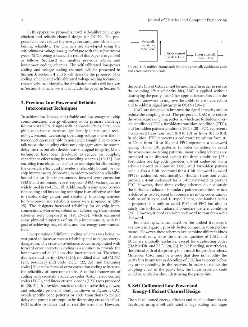
2 Journal of Electrical and Computer Engineering
In this paper, we propose a novel self-calibrated energy-efficient and reliable channel design for OCINs. The pro-posed channels reduce the energy consumption while main-taining reliability. The channels are developed using theself-calibrated voltage scaling technique with the self-correctedgreen (SCG) coding scheme. The rest of this paper is organizedas follows. Section 2 will analyze previous reliable andlow-power coding schemes. The self-calibrated low-powercoding and voltage scaling channels will be presented inSection 3. Sections 4 and 5 will describe the proposed SCGcoding scheme and self-calibrated voltage scaling technique,respectively. Additionally, the simulation results will be givenin Section 6. Finally, we will conclude the paper in Section 7.
2. Previous Low-Power and ReliableInterconnect Techniques
To achieve low latency and reliable and low-energy on-chipcommunication, energy efficiency is the primary challengefor current OCIN designs with nanoscale effects. First, cou-pling capacitance increases significantly in nanoscale tech-nology. Second, decreasing operating voltage makes the in-terconnection susceptible to noise increasingly. Due to cross-talk noise, the coupling effect not only aggravates the power-delay metrics but also deteriorates the signal integrity. Manytechniques have been developed to reduce the couplingcapacitance effect using bus encoding schemes [10–18]. Busencoding is an elegant and effective technique for eliminatingthe crosstalk effect, and provides a reliability bound for on-chip interconnects. Moreover, in order to provide a reliabilitybound for on-chip interconnects, forward error correction(FEC) and automatic repeat request (ARQ) techniques arewidely used in NoC [5, 19]. Additionally, a joint error correc-tion coding and bus coding technique is an effective solutionto resolve delay, power, and reliability. Encoding schemesfor low-power and reliability issues were proposed in [20–25]. The designers increased reliability for on-chip inter-connections. Moreover, robust self-calibrating transmissionschemes were proposed in [19, 26–28], which examinedsome physical properties of on-chip interconnects, with thegoal of achieving fast, reliable, and low-energy communica-tion.
Incorporating of different coding schemes was being in-vestigated to increase system reliability and to reduce energydissipation. The crosstalk avoidance codes incorporated withforward error correction coding is a solution to provide thelow-power and reliable on-chip interconnection. Therefore,duplicate-add-parity (DAP) [20], modified dual rail (MDR)[23], boundary shift code (BSC) [22, 23], and hammingcodes [20] are the forward error correction coding to increasethe reliability of interconnections. A unified framework ofcoding with crosstalk avoidance codes (CAC), error controlcodes (ECC), and linear crosstalk codes (LXC) was proposedin [20, 21]. It provides practical codes to solve delay, power,and reliability problems jointly as shown in Figure 1. CACavoids specific code patterns or code transitions to reducedelay and power consumption by decreasing crosstalk effect.ECC is able to detect and correct the error bits. However,
Crosstalkavoidance
code (CAC)
Error controlcode (ECC)
Linear crosstalkcode (LXC)
Figure 1: A unified framework for joint crosstalk avoidance codeand error correction code.
the parity bits of CAC cannot be modified. In order to reducethe coupling effect of parity bits, LXC is applied withoutdestroying the parity bits. Other approaches are based on theunified framework to improve the ability of error correctionand to address signal integrity in OCINs [20–25].
CACs are designed to improve the signal integrity and toreduce the coupling effect. The purpose of CAC is to reducethe worst-case switching patterns, which are forbidden over-lap condition (FOC), forbidden transition condition (FTC),and forbidden pattern condition (FPC) [20]. FOC representsa codeword transition from 010 to 101 or from 101 to 010.In addition, FTC represents a codeword transition from 01to 10 or from 10 to 01, and FPC represents a codewordhaving 010 or 101 patterns. In order to reduce or avoidthe worst-case switching patterns, many coding schemes areproposed to be directed against the three conditions [25].Forbidden overlap code provides a 5-bit codeword for a4-bit dataword to eliminate FOC. And forbidden patterncode is also a 5-bit codeword for a 4-bit dataword to avoidFPC in codeword. Additionally, forbidden transition codesprovide a 4-bit codeword for a 3-bit dataword to preventFTC. However, these three coding schemes do not satisfythe forbidden adjacent boundary pattern condition, whichis defined as two adjacent bit boundaries in the codes cannotboth be of 01-type and 10-type. Hence, one lambda codesis proposed not only to avoid FTC and FPC but also tosatisfy the forbidden adjacent boundary pattern condition[25]. However, it needs an 8-bit codeword to transfer a 4-bitdataword.
Joint coding schemes based on the unified frameworkas shown in Figure 1 provide better communication perfor-mance. However, these schemes just combine different kindsof codes directly, since the intrinsic qualities of CACs andECCs are mutually exclusive, except for duplicating codes(DAP, MDR, and BSC) [20, 23]. In DAP coding, nevertheless,the critical path of the priority bit is much longer than others.Moreover, CAC must be a code that does not modify theparity bits in any way as decoding of ECC has to occur beforeany other decoding in the receiver. In order to reduce thecoupling effect of the parity bits, the linear crosstalk codecould be applied without destroying the parity bits.
3. Self-Calibrated Low-Power andEnergy-Efficient Channel Design
The self-calibrated energy-efficient and reliable channels aredeveloped using a self-calibrated voltage scaling technique

Journal of Electrical and Computer Engineering 3
Rou
ters
ofot
her
nod
es
Joint bus and errorcorrection coding scheme
Self-calibratedlow swing
driver
Receiver
Router of the sender nodeVoltage control signal
Link wires
Green buscoding stage
(decoder)
Green buscoding stage
(encoder)
Sender
Self-calibratedvoltage scaling
(including errorcorrection decoder)
Voltage control signal
Router of the receiver node
Link wires
Triplication errorcorrection stage
(encoder)
Self-calibrated voltagescaling technique
Self-calibratedvoltage scaling
Switchingcircuits
Self-correctedgreen coding
Processorelement
Channel
Channel
Self-calibratedlow swing
driver
Processorelement
Self-calibratedvoltage scaling
(including errorcorrection decoder)
Triplication errorcorrection stage
(encoder)
Figure 2: Self-calibrated energy-efficient and reliable channels for on-chip interconnection networks with self-corrected green (SCG) codingscheme and self-calibrated voltage scaling technique.
and a joint bus/error correction coding scheme, which iscalled the SCG coding scheme. Figure 2 shows the blockdiagrams of the proposed channels for OCINs. The SCGcoding scheme reduces coupling effects and has a rapidcorrection ability that reduces the physical transfer unitsize in routers. The self-calibrated voltage scaling techniqueachieves the optimal operating voltage for link wires inchannels according to the SCG coding scheme. Additionally,the proposed technique overcomes increasing variation inadvanced technologies and facilitates the energy-efficienton-chip data communication. Therefore, the proposed self-calibrated low-power coding and voltage scaling realizeenergy-efficient and reliable channels for OCINs.
The SCG coding scheme is a joint bus and error cor-rection coding scheme that provides low-energy and highreliability channels for OCINs. The SCG coding scheme isconstructed in two stages, the green bus coding stage andthe triplication error correction coding stage. In routers, anundecoded code increases the area and energy dissipationof switching circuits by large physical transfer unit sizes.Therefore, the error correction code should be decoded inrouters to reduce power dissipation and the area of switchingcircuits and buffers. The triplication error correction codingstage achieves rapid correction to reduce the physical transferunit size in routers via a self-corrected mechanism at thebit level. To efficiently reduce the coupling effect, the green
bus coding stage is developed using the joint triplicationbus power model, which depends upon the characteristicsof triplication error correction coding. The SCG coding canavoid the FOC and FPC, and reduce the FTC to achieve thepower saving of channels. The bit width in the self-calibratedlow-power coding and voltage scaling varies. The green buscoding encodes packets in accordance with a 4-to-5 codec.To increase the reliability of channels, the triplication errorcorrection stage increases bit width from k-bit to 3k-bit.Although the SCG coding increases link wires in channels,on-chip wires are cheap and plentiful with the increasingmetal layers in advanced technologies [29, 30].
Designers can tradeoff between power consumption andreliability by reducing the operating voltage as the errorcorrection coding increases the reliability of channels. There-fore, the operating voltage of the link wires in channels isadjusted according to the SCG coding scheme using a self-calibrated voltage-scaling technique. This technique detectserror conditions of channels in the triplication error cor-rection stage, and thus feeds the control signals back tothe low swing drivers and adjusts the operating voltage ofthe link wires. The self-calibrated voltage scaling techniquedetermines the optimal operating point to trade off betweenenergy consumption and reliability. The SCG coding schemeand self-calibrated voltage scaling technique are described inSections 4 and 5, respectively.

4 Journal of Electrical and Computer Engineering
4. Self-Corrected Green (SCG) Coding Scheme
This section describes the SCG coding scheme, a joint busand error correction coding scheme. This proposed schemegenerates low-energy and reliable channels for advancedtechnologies. The SCG coding scheme is constructed viatwo stages, the green bus coding stage and triplication errorcorrection coding stage. The green bus coding has the advan-tages of shorter delay for error correction coding, greaterenergy reduction, and smaller area than other approaches.The green bus coding is developed using the joint triplicationbus power model to achieve additional energy reductions fortriplication error correction coding.
4.1. Triplication Error Correction Stage. The triplication errorcorrection coding scheme as shown in Figure 3 is a singleerror correcting code by triplicating each bit. Based oninformation theory, a code set with a hamming distance ofh has an h − 1 error-detect ability and a [(h − 1)/2] error-correction ability. For triplication error correction coding,the hamming distance of each bit is 3. Therefore, each bitcan be corrected individually when no more than one errorbit exists in the three triplicated bits, which are defined as atriplication set. The error bit can be corrected by a majoritygate. Figure 3 also shows the function of the majority gate.Compared with other error correction mechanisms, thecritical delay of the decoder is a constant delay of a majoritygate and significantly smaller than that of other approaches[19–25]. Restated, the triplication error correction codinghas rapid correction ability via self-correction mechanism atthe bit level. Therefore, triplication error correction codingis more suitable to OCINs because data can be decoded andencoded in each router using the small delay of triplicationcorrection coding.
Additionally, one advantage of incorporating error cor-rection mechanisms in an OCIN data stream is that thesupply voltage of channels can be reduced without compro-mising the system reliability. Reducing supply voltage, Vdd,increases bit error probability. To simplify error sources, weassume bit error probability, ε, is as in the following equationwhen a Gaussian distributed noise voltage, VN , with varianceσ2N is added to the signal waveform:
ε = Q(Vdd
2σN
), (1)
where Q(x) is given as
Q(x) = 1√2π
∫∞xe−y
2 /2dy. (2)
Each triplication set can be error-free if and only if no errortransmission exists or just 1-bit error transmission exists. Foreach triplication set, P1-bit correct is given as
P1-bit correct = (1− ε)3 +
⎛⎝3
1
⎞⎠ε(1− ε)2. (3)
x0
x1
xk−1
Triplication
Channels
Majority gate
FM
Decoder
x0
x1
xk−1
abc
FM = ab + bc + ca
···
···
···
Figure 3: Triplication error correction stage of SCG coding scheme.
For k-bits data, transmission is error-free if and only ifall k triplication sets are correct. Thus, Pk bits correct is givenby
Pk bits correct =k∏
i=1
Pi-bit correct =(1− 3ε2 + 2ε3)k.
(4)
Hence, word-error probability is
Ptriplication = 1− (1− 3ε2 + 2ε3)k. (5)
For a small probability of bit error, ε, (5) is simplified to
Ptriplication ≈ 3kε2 − 2kε3. (6)
By contrast, word-error probability is much smaller than thatin the Hamming code and Duplicate-add-parity (DAP) [20,21] which are directed to k2ε2. Triplication error correctioncoding can avoid the FOC and FPC which increase energydissipation via the coupling effect.
Because error-correction coding increases the reliabilityof on-chip interconnections, designers can tradeoff betweenpower consumption and reliability by reducing operatingvoltage. In simplifying the cumulative effect of noise sources,the noise model on interconnects assumes Gaussian dis-tributed noise with voltage VN and variance σ2
N is added tothe signal. In addition, we assume errors on different linklines are independent. The bit error probability, ε, is givenin (1) and (2), where Vdd is signal voltage swing. With giventhe same σ2
N , the bit error probability is increasing as thesignal voltage swing decreases. However, some specific errorcontrol/correct coding schemes can decrease signal voltageswing, and guarantee the reliability of interconnections, ifand only if the following equation is satisfied:
Puncode(ε) ≥ PECC(ε), (7)
where ε is bit error probability with full swing voltage of1.0 V, and ε is bit error probability with a lower swingvoltage. To obtain the lowest supply voltage for specific error

Journal of Electrical and Computer Engineering 5
correction coding under the same level of reliability of theuncoded code, supply voltage can be revised as
Vdd = VddQ−1(ε)Q−1(ε)
, Puncode(ε) = PECC(ε).
(8)
The inverse function of the Gaussian distributed function isalso called a probit function Φ(x). The probit function hasproved that the function does not have primary primitive.To solve the problems, this work first approximates the biterror probability by varying voltage swing. By integratingfrom 100 − Vdd/2, the integral range on the x-axis isdivided into 0.0001 (V) segments, and each segment canproduce a trapezoid. The areas of all trapezoids are thensummed, which is the approximation of bit error probability.Therefore, the lowest voltage swing for a specific errorcorrection coding that satisfies (8) can be obtained.
When an uncoded code is operated at full swing supplyvoltage (1.0 V), different levels of bit error probability, ε,can be obtained by altering the variance of the Gaussiandistributed function. Figures 4(a) and 4(b) show the voltagesof specific error correction coding versus different uncodedword error rates with k = 8 and k = 32, respectively.Factor, k, is bit width. If bit error probability of anuncode word, ε, is 10−20, the specific voltage of ham-ming code [20], duplication-add-parity code [20, 21], jointcrosstalk avoidance and triple-error-correction code (JTEC)[24] and the proposed SCG code are 0.705 V, 0.710 V, 0.579 V,and 0.696 V, respectively. The JTEC code uses a doubleerror correction coding stage to enhance error correctionand obtains lower voltages. However, delay and area over-heads of the JTEC are much worse than those of otherapproaches. Compared to other ECC codes, the proposedSCG code has better characteristics in that the lowest supplyvoltage increases slowly when the uncoded word error rateincreases.
4.2. Joint Triplication Bus Power Model. Although tripli-cation error correction coding can avoid many forbiddenconditions, some power-hungry transition patterns cannotbe eliminated entirely. These patterns are mainly generatedby the FTC and self-switching activity. The FTC can besatisfied when a bit pattern does not have a transition from01 to 10 or from 10 to 01. This work modified the RLC cyclicbus model in [31] by considering loading capacitances andcoupling capacitances. Figure 5(a) shows the modified modelwith a four-bit bus, where C1 means the loading capacitanceof line 1 and the C12 is the coupling capacitance between line1 and line 2. Moreover, the bus lines are parallel and coplanar.Most of the electrical field is trapped between adjacentlines and the ground. Figure 5(b) shows an approximate buspower model that ignores the parasitic capacitances betweennonadjacent lines.
We assume all grounded capacitors have the same valuewithout considering the fringing effect of boundary lines,because fringing capacitors are much smaller than loadingand coupling capacitors, even for the wide buses. Therefore,this work utilized a joint triplication bus model to implement
k = 8
Vol
tage
(V)
0.56
0.6
0.64
0.68
0.72
−26 −24 −22 −20 −18 −16 −14 −12 −10 −8 −6
DapHammingJTEC
SCG (triplication)
log10(uncoded word-error-rate)
(a)
k = 32
0.7
0.75
0.8
0.85
0.9
0.95
DapHammingJTEC
−26 −24 −22 −20 −18 −16 −14 −12 −10 −8 −6
Vol
tage
(V)
SCG (triplication)
log10(uncoded word-error-rate)
(b)
Figure 4: The corresponding voltages of specific error correctioncoding versus different uncoded word-error-rate with (a) k = 8 and(b) k = 32.
the bus coding stage to further reduce energy consumption.For a 4-bit triplication bus, the capacitance matrix Ct can beexpressed as
Ct =
⎡⎢⎢⎢⎢⎢⎢⎣
3 + λ −λ 0 0
−λ 3 + 2λ −λ 0
0 −λ 3 + 2λ −λ0 0 −λ 3 + λ
⎤⎥⎥⎥⎥⎥⎥⎦CL, λ = CX
CL.
(9)
The parameter, λ, is defined as the ratio of coupling capaci-tance,Cx, to loading capacitance,CL. Therefore, the λ param-eter depends on the technology, the specific geometry, themetal layer, and bus shielding. λ has some important prop-erties; for example, the parameter λ typically increases with

6 Journal of Electrical and Computer Engineering
C1 C2 C3 C4
C12
C13
C14
C23
C24
C34
(a) (b)
C1 C2 C3 C4
C12 C23 C34
Figure 5: (a) Bus model for 4 bits. (b) The approximate bus powermodel.
technology scaling. For instance, the value of λ is between6 and 10, depending on the metal layer for standard 65 nmCMOS technology and the minimum distance betweenwires. The parameter λ should be much larger in advancedtechnologies. Additionally, the coefficient of loading capaci-tances is 3 for the three triplicated bits.
Five transition states exist between two adjacent lines,four of which are described in [32]. These five types can beseparated into two cases. The first case is static transitions,including type I (single line switching), type II (two linesswitching in opposite directions), and type III (no switchingor two lines switching in the same direction) as shown inFigure 6. The other case is dynamic transitions which includetype IV and type V with signal aliasing for type II andtype III, respectively. The static transition is defined as twoadjacent lines switching at the same time without noise ordifferent delays. The dynamic transition means that the twoadjacent lines may be misaligned.
The power consumption formula is shown in (10), whereE and P are energy and power density, respectively; f andV (Vdd) are frequency and voltage (voltage supply), respec-tively. Bi is the current voltage level (1 or 0) for line i, and B−1
i
is the previous voltage level for the line i;
E =(V f)T
Ct(V f −Vi
),
P = f ∗V 2dd∗∑
i
∑
j
Ct{(Bi − B−1
i
)∗(Bj − B−1
j
)}.
(10)
Power density, P, can be transferred into
P = f ∗C∗L V2dd
∗
⎧⎪⎪⎪⎪⎪⎨⎪⎪⎪⎪⎪⎩
3(B1 − B−1
1
)2+ 3(B2 − B−1
2
)2+ 3(B3 − B−1
3
)2
+3(B4 − B−1
4
)2+ λ[(B1 − B−1
1
)− (B2 − B−12
)]2
+λ[(B2 − B−1
2
)− (B3 − B−13
)]2
+λ[(B3 − B−1
3
)− (B4 − B−14
)]2
⎫⎪⎪⎪⎪⎪⎬⎪⎪⎪⎪⎪⎭.
(11)
The items in (11) are defined and identified as follows:(Bi − B−1
i
)2 = Bi ⊕ B−1i = ri,
[(Bi − B−1
i
)−(Bj − B−1
j
)]2 = ri ⊕ rj + 4× di j ,
where di j = BiB−1i BjB
−1j ∪ BiB
−1i B jB−1
j .
(12)
L
H
Type I L
LH
Type II HL Type III
L
Static transitions
Dynamic transitions
L
H
Type IV
L
HType VL
HL
H
Aliasing
L
Cx Cx Cx
CxCx
Figure 6: Five transition types for two adjacent wires.
The ri means that a switch of line i exists and is not concernedwith the direction of change and adjacent lines. This item, ri,only considers loading capacitances. The meaning of ri ⊕ rjis that only one line is changing between two lines of i andj (Type I). Additionally, di j indicates that two lines changein opposite directions (Type II and Type V). Moreover,compared with the other two definitions, ri and ri ⊕ rj , thevoltage difference across the coupling capacitance is doubleand when squared it factors 4 for di j . Using (12), the powerformula can be obtained as (13) with the parameter of λ.The term α is the coefficient of coupling effects and switchingactivities. Except for Type IV, the five transition states are allconsidered in this power formula:
P = f × CL × V 2dd × α,
α = 3(r1 + r2 + r3 + r4) + λ(r1 ⊕ r2 + r2 ⊕ r3 + r3 ⊕ r4)
+ 4λ(d12 + d23 + d34).(13)
4.3. Green Bus Coding Stage for Crosstalk Avoidance. The pur-pose of the green bus coding stage is to minimize the valueof α in (13) by encoding signals when λ > 2. Figure 7shows design flow of green bus coding. First a triplicationcapacitance matrix is established using the RLC cyclic model.Then the power formula with coefficient α is derived, whereα represents the switching factor by considering couplingcapacitances. The green bus coding stage only affects coef-ficient α. Furthermore, the codeword minimizes the value ofα and maps the codeword to the dataword. Depending on themapping between the codeword and dataword, the green buscoding stage can be implemented.
According to the design flow of the green bus codingstage, the modified switching activity, α, should be mini-mized. Therefore, to converter the 4-bit dataword into a 5-bit codeword, a 32×31 transition state table is established bycalculating α. Thus, 16 transition patterns are selected withminimal values of α as the codeword to eliminate crosstalk.The green bus coding chooses a 4 : 5 code to minimizeα depending on the energy saving bound and the latencyof codec. In a data bus, the bit width of a data is usually

Journal of Electrical and Computer Engineering 7
Derive power formulawith the coefficient α
Find the codeword tominimize the value, α
Circuit implementation
Transitiondefinition
Establish triplication
capacitance matrix Ct byRLC cyclic model
Map the codeword todataword
Figure 7: The design flow of the green bus coding stage.
a multiple of 4. Therefore, the energy-saving bound of 4 : 5 to4 : 8 codes are between 40% to 55% from the energy-savingbound analysis of [33]. However, the latency of the codec willincrease significantly as the size of a codeword increases.
Figure 8(a) shows the relationships between the 4-bitdataword and 5-bit codeword. According to the relation-ships, the data-word can be grouped into two sets, the origi-nal set and the converted set as shown in Figure 8(b). Whentransmitted data are in the converted set, the green buscoding stage converts the data into the original set via one-on-one mapping. Meanwhile, the converted bit, c4, will beasserted, and c0 and c2 will be inverted and mapped to theoriginal set. Notably, x1 and x3 will always not be modified.
Figure 9 shows the circuit implementation of green buscoding, including the encoder and decoder. The circuitry ofgreen bus coding is more simple and effective than otherapproaches using the joint triplication bus model. An extrashielding line to reduce the coupling effect is not neededbetween two adjacent 5-bit codewords because the boundarydata of the 5-bit codeword are set to roughly 0. Table 1 showsthe comparisons between green bus coding and increasingwire spacing when λ = 8. Although increasing wire spacingcan achieve more energy reduction than green bus coding, ithas great amount of area overhead. Additionally, the energy-delay product (EDP) of green bus coding is smaller than thatof double wire spacing.
The proposed green bus coding stage has the followingproperties.
(1) Use c4 as the detection bit to decode c0 and c2. Itcan simplify the circuitries of encoder and decoder,especially that of the decoder.
(2) The encoded bit always equals the data bit at certainbit positions, where c1 = x1 and c3 = x3.
C4 = X2X1X0
+X3X2X0
+X3X2X1
CodewordsX∼3 X0 C∼4 C0
0 0 0 0
0 0 0 1
0 0 1 0
0 0 1 1
0 1 0 0
0 1 0 1
0 1 1 0
0 1 1 1
1 0 0 0
1 0 0 1
1 0 1 0
1 0 1 1
1 1 0 0
1 1 0 1
1 1 1 0
1 1 1 1
0 0 0 0 0
0 0 0 0 1
0 0 0 1 0
0 0 0 1 1
0 0 1 0 0
1 0 0 0 0
0 0 1 1 0
0 0 1 1 1
0 1 0 0 0
1 1 1 0 0
1 1 1 1 1
1 1 1 1 0
0 1 1 0 0
1 1 0 0 0
0 1 1 1 0
0 1 1 1 1
(a)
0000
1000
1100
1110
1111
0001
0010
0011
0100
0110
0111
0101
1101
1001
1011
1010
Converted set
if (C4 = 1) then
C0 = X0, C2 = X2
else
C0 = X0, C2 = X2
(b)
Original setDatawords
Figure 8: (a) The mapping table between 4-bit dataword and 5-bit codeword of the green bus coding stage. (b) The two sets andBoolean expression of the green bus coding stage.
Encoder Decoder
x0
x1
x2
x3
c0
c1
c2
c3c4
c0c1
c2
c3
c4
x0
x1
x2
x3
Figure 9: The encoder and decoder of green bus coding stage.
(3) By focusing on the joint bus and error correction cod-ing scheme, the SCG coding scheme can avoid FOCand FPC and reduce FTC to further reduce powerconsumption.
(4) Adding extra shielding lines to reduce the couplingeffect between two adjacent codeword with increas-ing coding bits is unnecessary.
(5) According to the delay model and energy model givenby [33], the energy dissipation and critical delay arereduced from (1 + 1.5λ)CV 2 to (1.18 + 1.17λ)CV 2
and (1 + 4λ)τ0 to (1 + 2λ)τ0 via the green bus coding,respectively. τ0 is defined as the delay of a crosstalk-free wire.
5. Self-Calibrated Voltage Scaling Technique
The proposed self-calibrated voltage scaling technique is ap-plied to reduce the operating voltage of channels for energy
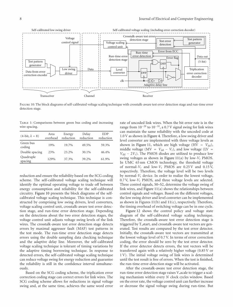
8 Journal of Electrical and Computer Engineering
Low swingdriver
clk
Error flag
Adaptive delay line
Data from errorcorrection encoder
DFF
Triplicationerror correction
decoder
Test patterngenerator
Testdetection
Data out
Transceiver ReceiverChannel
Run-time errordetection stage
Crosstalk-aware test errordetection stage
Levelconverter
Voltage scalingcontrol unit
Run-timeerror detection
Self-calibrated low swing driver Self-calibrated voltage scaling (including error correction decoder)
Error from ECC
(5-bit)
Voltagecontrol signal
DataDFF
Test patterngenerator
error
Figure 10: The block diagrams of self-calibrated voltage scaling technique with crosstalk-aware test error detection stage and run-time errordetection stage.
Table 1: Comparisons between green bus coding and increasingwire spacing.
(4-bit, λ = 8)Area
overheadEnergy
reductionDelay
reductionEDP
reduction
Green buscoding
19% 19.7% 49.5% 59.3%
Double spacing 23% 23.2% 30.1% 46.4%
Quadruplespacing
129% 37.3% 39.2% 61.9%
reduction and ensure the reliability based on the SCG codingscheme. The self-calibrated voltage scaling technique willidentify the optimal operating voltage to trade off betweenenergy consumption and reliability for the self-calibratedcircuitry. Figure 10 presents the block diagrams of the self-calibrated voltage scaling technique. This technique is con-structed by comprising low swing drivers, level converters,voltage scaling control unit, crosstalk-aware test error detec-tion stage, and run-time error detection stage. Dependingon the detections about the two error detection stages, thevoltage control unit adjusts voltage swing levels of the linkwires. The crosstalk-aware test error detection stage detectserrors by maximal aggressor fault (MAF) test patterns inthe test mode. The run-time error detection stage detectserrors using the double sampling data checking techniqueand the adaptive delay line. Moreover, the self-calibratedvoltage scaling technique is tolerant of timing variations bythe adaptive timing borrowing technique. In response todetected errors, the self-calibrated voltage scaling techniquecan reduce voltage swing for energy reduction and guaranteethe reliability is still in the confidence interval simultane-ously.
Based on the SCG coding scheme, the triplication errorcorrection coding stage can correct errors for link wires. TheSCG coding scheme allows for reductions in signal voltageswing and, at the same time, achieves the same word error
rate of uncoded link wires. When the bit error rate is in therange from 10−20 to 10−10, a 0.7 V signal swing for link wirescan maintain the same reliability with the uncoded code at1.0 V as shown in Figure 4. Therefore, a low swing driver andlevel converter are implemented with three voltage levels asshown in Figure 11, which are high voltage (HV = Vdd),middle voltage (MV = Vdd − Vt), and low voltage (LV =Vdd − 2Vt). The PMOS diodes are utilized to produce lowswing voltages as shown in Figure 11(a) by low-Vt PMOS.In UMC 65 nm CMOS technology, the threshold voltageof normal-Vt and low-Vt PMOS are 0.25 V and 0.15 V,respectively. Therefore, the voltage level will be two levelsby normal-Vt device. In order to realize the lowest voltage,0.7 V, low-Vt PMOS, and three voltage levels are selected.Three control signals, S0–S2, determine the voltage swing oflink wires, and Figure 11(a) shows the relationships betweencontrol signals and voltages. Based on the different voltages,the low swing driver and level converter can be implementedas shown in Figures 11(b) and 11(c), respectively. Therefore,the timing overhead of switching voltage can be in one cycle.
Figure 12 shows the control policy and voltage statediagram of the self-calibrated voltage scaling technique.Therefore, the crosstalk-aware test error detection stage istriggered by T start, and crosstalk-aware test vectors are gen-erated. Test results are compared by the test error detector.Initially, the crosstalk-aware test vectors are transmitted atthe lowest voltage level of 0.7 V. In terms of error correctioncoding, the error should be zero by the test error detector.If the error detector detects errors, the test vectors will betransferred again with a relatively higher voltage (0.85 V or1 V). The initial voltage swing of link wires is determineduntil the test result is free of errors. When the test is finished,the run-time error-detection stage will be activated.
After the crosstalk-aware test error detection stage, therun-time error detection stage raises V scale to trigger a scal-ing mechanism within every N clock cycles window. Basedon the error rate, the voltage control unit can further increaseor decrease the signal voltage swing during run-time. But

Journal of Electrical and Computer Engineering 9
(a)
(b) (c)
In
S0S1S2
Low Vt10
S0S1S2
1
1
11 0
0 1
InOutOut
Vdd
VddL
Vdd VddL
Vdd
VddL
Vdd
Vdd
VddL
Vdd
Vdd − 2|Vtp|
Vdd − |Vtp|
VddL
Figure 11: (a) Low swing voltages. (b) Low swing driver. (c) Levelconverter.
the voltage in the run-time error detection stage cannot belower than the voltage level determined by the crosstalk-aware test error detection stage. The error rate is defined asthe ratio of the error data to the total transmission data inone window. If the error rate is less than 5%, signal voltageswing is reduced one level or kept at the lowest safe signal.However, if the bit error rate is larger than 5% but less than15%, the signal voltage swing level is the same as that for theprevious window. If the error rate is larger than 15%, signalvoltage swing is increased one level or kept at the highestsignal swing level. The range of bit error rate detectiondepends on properties of SCG coding scheme. If uncodedinput data are random, the probability of the forbiddenpattern condition (two adjacent lines switch in oppositedirections, e.g., ↑↓ or ↓↑) of the coding scheme is roughly15%. Additionally, the 5-bit voltage scaling control unit candetermine 5% and 15 % error rate by an 8-bit adder in 256cycles (detection window).
5.1. Crosstalk-Aware Test Error Detection Stage. The cross-talk-aware test error detection stage is composed of a testpattern generator (TPG), a test error detector (TED), and acontrol unit that generates the control voltages for the lowswing driver. The crosstalk-aware test error detection stageis triggered by T start, and then generates crosstalk-awaretest vectors. Conventional test pattern generators, such asthe liner feedback shift register (LFSR) [34, 35], generatepseudorandom pattern sequences. By changing the feedbackpolynomial of the LFSR, the LFSR generates different subsetsof the maximum-length LFSR (maximum 2n − 1 patternswhen the LFSR tests n-bits data with primitive polynomials).However, test patterns generated by the LFSR-based TPG arecomplicated and require a long test time to achieve high errorcoverage. Hence, a better self-test methodology is needed to
achieve low hardware overhead, fast test time, and high errorcoverage.
Depending on test vectors, therefore, the test error detec-tor can detect error data following error correction coding.The crosstalk-aware test vectors are generated by a testpattern generator with the maximal aggressor fault (MAF)model as shown in Figure 13 [36]. The MAF-based test pat-terns are a simple pattern stream that represents six differentcrosstalk effects: rising speedup (Sr), falling speedup (Sf),rising delay (Dr), falling delay (Df), positive glitch (Gp), andnegative glitch (Gn). For test wires with n-bits, one victimline and n− 1 aggressor lines exist. All aggressor lines switchsimultaneously to generate speedup, delay, or glitch error onthe victim line. The MAF test vectors can achieve high errorcoverage. Additionally, the MAF-based test can be consideredas an aggressive test that covers other pattern transition cases.To test n-bit on-chip interconnects, six fault models mustbe tested on each line. Therefore, testing n-bit needs 6n testpattern transitions to complete an MAF-based test.
The test pattern generator of the MAF-based self-testmethodology is implemented by the finite state machine(FSM). The FSM needs a minimum of 8 cycles to completesix faults tests on one victim line, indicating that the test pat-tern generator requires 8n cycles to complete an n-bit MAFtest. Test time is much shorter than that of the linear feedbackshift register. The FSM, which is triggered by T start signal,generates the values of the victim line and the aggressor line,counter reset (C reset) and counter enable (C enable). Aftereach circle (states S1–S8) of the FSM, C enable triggers thevictim counter. The decoder and output 2-to-1 MUX areselected to ensure that the data bit (Di) selects the correctvalue (victim or aggressor value) during the test. When thevalue of the victim counter (C value) is equal to n− 1 in theS8 state, the test is finished and returns to the S0 state.
5.2. Run-Time Error Detection Stage. The run-time error de-tection stage detects timing variations of link wires. Timingdelay variations of on-chip interconnections are due tocrosstalk noise, process variations, temperature variations,and other noises. To overcome timing error, the master-slaveflip-flop (MSFF) [37] and double sampling data checkingtechnique [38] have been proposed to detect timing errors.The MSFF contains a master flip-flop and a slave flip-flop,both of which operate at the same frequency. However, theslave flip-flop is positively triggered by a delay clock (Δt)which is proportion to master flip-flop. We assume the datacaptured by the slave flip-flop is correct. The data capturedby the master flip-flop and the slave flip-flop are comparedusing an XOR gate; an error-flag is generated when the twodata are not identical. When an error occurs, the controlcircuit stalls pipeline data flow for 1 clock and the slave flip-flop resends correct data to the master flip-flop. The principleof the double sampling data checking technique is similar tothat of the MSFF.
The timing delay variation of on-chip interconnects af-fects the design on Δt. The different propagation delay on theon-chip interconnection caused by crosstalk is due to differ-ent pattern transients. For the increasing timing variation of

10 Journal of Electrical and Computer Engineering
Start
Crosstalk-awaretest error detection
Raise testvoltageswing
No
Yes
Yes No
Error free
Run-time errordetection
Voltagescaling for
next windowError rate < 5%: (fall)
5% < error rate < 15%: (stay)15% < error rate: (raise)
LV
MV
HV
Detection window: 256 cycleVoltage switching: 1 cycle
Yes
Different detect bits error rate
V scale = 1
T start = 1
Figure 12: The control policy of self-calibrated voltage scaling technique.
State
s1Sr
Sf
Gp
Dr
Df
Gn
State machine
Victim counter
Select decoder
Sel0
Sel1
Seln− 1
VictimAggressor
D0 D1 Dn−1
S0
S1
S2 S8
S4
S5
S6
S3 S7
(a) (b)
Victim Aggressor
0
1
0
1
0
1
1
0
0
0
1
0
1
1
0
1 s2
s3
s4
s5
s6
s7
s8
C reset
C enable
T start = 1
T start = 0
C value = n− 1
C value
Figure 13: MAF-based test pattern generator (a) 8 states complete 6 faults test of MAF model. (b) Hardware implementation.
on-chip interconnections, detecting timing error is difficultfor various voltage levels. However, the MSFF and doublesampling data checking technique are limited by the clockperiod and fixed delay line, respectively. Therefore, the run-time error detection stage is constructed using the adaptivetiming borrowing technique as shown in Figure 10. Theadaptive timing borrowing technique modifies the doublesampling data checking technique with the adaptive delayline. In addition, the adaptive timing borrowing technique
also has correction ability via a multiplexer. The modifieddouble sampling data checking technique with the adaptivedelay line has the adaptive timing borrowing ability toborrow timing from the next clock period.
Figure 14 presents analytical results for timing con-straints. To ensure that functionality of the modified doublesampling data checking technique is correct, time interval Δtmust be set appropriately, and each pipeline stages must beconsidered. If the delay between DFF1 and DFF2 exceeds l

Journal of Electrical and Computer Engineering 11
D QDFF
01
Error correctiondecoder
DFF
clk
DFF
clk
InputOutput
DFF1 DFF2 DFF3 DFF4
Low swingdriver Level converter
Link wires
tDFF tXOR
d clk
1
2
3
4
5
(a) (b) (c)
Error freeDelay errordetected!!
Glitch errordetected!!
!!
td td
Δt Δt Δt
Δt
1 2 3 4 5
DFFD QD Q
D Q
clkclk
Figure 14: Modified double sampling data checking circuit and waveforms. (a) Error-free. (b) Delay error. (c) Glitch error.
clock cycle, error sampling data of DFF1 are induced. Themaximum data path delay can be extended to 1 clock cycleplus time interval Δt, as in (14), where tDFF is the clock to Qdelay of the D flip-flop, and td is the data path delay (fromthe input of the low swing driver to the output of the levelconverter), tXOR is the XOR propagation delay, and tsetup isthe setup time of the D flip-flop,
tDFF1 + td + tXOR + tsetup3 < τclk + Δt. (14)
DFF3 samples the comparison signal, which compares sam-pling data before DFF2 and after DFF2. In addition, DFF3must sample the comparison signal before next datum ar-rives. Therefore, Δt should be satisfied as
tDFF2 + tXOR + tsetup3 < Δt < tDFF1 + td + tXOR + tsetup3.(15)
Additionally, the pipeline stages after the double samplingdata checking stage must satisfy basic constraints, as inthe following equation, to avoid the excessive timing borrow-ing:
Δt + tDFF3 + tMUX + tDecoder + tsetup4 < τclk. (16)
Equations (14) and (15) are the timing conditions that avoiderror detections, (16) is the timing condition that prevents
setup timing violation of the sequential circuitry. Accordingto (14)–(16), the upper and lower bounds of time interval Δtare derived by the following equation. When the time intervalΔt is appropriate, the run-time error detection stage correctserror data and provides run-time error rate information, al-lowing the self-calibrated voltage scaling technique to adjustthe voltage swing levels of link wires:
Max{(
tDFF1 + td + tXOR + tsetup3 − τclk
),
(tDFF2 + tXOR + tsetup3
)}
< Δt < Min{(
tDFF1 + td + tXOR + tsetup3
),
(τclk − tDFF3 + tMUX + tDecoder + tsetup4
)}.
(17)
If (14) is not satisfied, a type I statistical error occurs. Thedouble sampling data checking technique cannot detect trueerrors, and suppose that the sampling data would be correct.On the other hand, if (15) is not satisfied, the type II sta-tistical error occurs. The double sampling data checkingtechnique then misjudges and asserts an error flag when thetransferred data is correct.
12 Journal of Electrical and Computer Engineering
2 4 6 8 10
−60
−40
−20
0
20
40
Ave
rage
ED
Psa
vin
gov
eru
nco
ded
wor
d(%
)
Ratio of coupling capacitance toloading capacitance (λ)
HammingFTC-HCFOC-HCOLC-HCBSC
DAPDSAPJTECTriplicationSCG
Triplication error correction stage
SCG coding scheme
EDP savingimproved by green
bus coding stage
(a)
20
30
40
50
60
70
HammingFTC-HCOLC-HCBSC
DSAPJTECSCG
2 4 6 8 10Ratio of coupling capacitance to
loading capacitance (λ)
Ave
rage
ED
Psa
vin
gov
eru
nco
ded
wor
d(%
)
SCG coding scheme
(b)
Figure 15: The energy-delay product (EDP) reduction to uncoded code under different values of λ with (a) full swing signal and (b) thelowest swing signal.
Link wires
RouterGreen bus
coding stage(encoder)
Router
N routers, N − 1 segments for channels
Router architecture
Switchingcircuits
BufferRouting andarbitration
Headerdecoder
Error correctionstage (decoder)
Switchsetup
Channel
1st stage 2nd + 3rd stage 4th stage
Router
Channel
RouterGreen bus
coding stage(decoder)
Error correctionstage (encoder)
(Cu, metal-06, M μm)
Figure 16: Simulation environment setup with different number of routers (N) and different lengths (M) of link wires.
Timing delay variation is caused by the crosstalk effect,process variation, width variation, and voltage variation. Inview of increasing timing variation, the adaptive delay line isan effective solution that satisfies these conditions. Further-more, data path delay td is affected significantly by operatingvoltages and input vectors. Therefore, the adaptive delay linecan generate three time intervals Δt for different signalvoltage levels to satisfy the timing condition in (17); thus, theadaptive delay line can be implemented by a digital controldelay line with MUXs. Adjusting the time interval Δt guar-antees the functionality of double sampling data checkingtechnique with different voltage swing levels and processvariations.
6. Simulation Results
This section presents simulation results demonstrating theimprovement in energy and reliability via the SCG codingscheme and the self-calibrated voltage scaling technique.All simulation results are based on UMC 65 nm 1P9MCMOS technology. For OCINs, the metal layers can becategorized into upper-level, middle-level, and lower-level,respectively. In most cases [39–41], the upper-level metallayers are routed for power grids and global clock distribu-tion via low resistance metals. Additionally, the lower-levelmetal layers are routed for local resources. Therefore, thecharacteristics of link wires between interprocessor elementsare set as metal-6 with a minimum width and spacing of
Journal of Electrical and Computer Engineering 13
0.10 μm in UMC 65 nm 1P9M CMOS technology. Simu-lation results include analysis of different error-correctioncoding schemes, energy-delay product (EDP) of differentjoint coding schemes, energy saving of SCG coding in an8 × 8 mesh network, process-variation timing analysis, andanalysis of the self-calibrated voltage scaling technique.
Table 2 lists different combinations of joint codingschemes, such as the hamming code (HC), FTC+HC,FOC+HC and boundary shift code (BSC) in [23], one lumb-da code (OLC)+HC and DAP+shielding (DSAP) in [25],JTEC in [24], and the proposed SCG coding scheme. Addi-tionally, Table 2 summarizes different joint coding schemesfor 8-bit link wires, which consist of the physical transferunit size in channels and routers, the maximum delay andaverage energy of link wires, and the corresponding lowestsupply voltage. Table 2 also summarizes the codec of differentapproaches, including the corresponding codec area, power,and latency. The lowest supply voltages are theoretical valuesfrom Figure 5 when ε = 10−20. The JTEC uses double errorcorrection coding to enhance error correction. However,codec overhead and energy dissipation (unoptimized JTECfor 8-bit) are much worse than those of other approaches.Although the JTEC can reduce the supply voltage to thelowest point at the same uncoded word-error-rate, thelatency is larger than others due to long chains of XOR gates.Furthermore, the lowest voltage of JTEC increases rapidly asbit error rate increases.
Except for the SCG coding, DAP and DSAP, the criticaldelays of other codec are larger than 0.5 ns. Consequently,these codecs are not appropriate for integration into high-speed routers. Therefore, the physical transfer unit sizes inrouters of these codecs are bigger than that of proposedcoding scheme; thus network area and energy consumptionincrease. The delay of green coding stage and triplicationerror correction stage are 0.28 ns and 0.09 ns, respectively.And the power consumption of triplication error correctionstage is only 41.5 μW. Hence, the proposed SCG codingscheme has the smallest codec overhead. Additionally, thegreen bus coding stage is only integrated in the sender nodeand receiver node.
The delay and energy of link wires are calculated via thedelay model and energy model given by [33], where τ0 isdefined as the delay of a crosstalk-free wire. The proposedSCG coding scheme achieves the most energy reduction byreducing coupling effects on link wire, and avoids the FOCand FPC by the triplication error correction coding stage.Additionally, the SCG coding scheme can reduce the FTCand self-switching activities using the green bus coding stagedepending on the joint triplication power model. Althoughthe triplication error correction stage triplicates transferreddata and increases the physical transfer unit size on linkwires, it also enhances data reliability and avoids the worstcrosstalk patterns. Moreover, the delay can be reduced from(1 + 4λ)τ0 to (1 + 2λ)τ0.
Figure 15(a) shows the energy-delay product (EDP) re-duction compared to uncoded code under different λ values.Coefficient λ is defined as the ratio between coupling capac-itance of two adjacent lines and loading capacitance. Theenergy and the delay are measured as the average energy
200 400 600 800 1000 1200 1400 1600 1800
0
10
20
30
40
N = 8N = 16N = 24N = 32N = 40
N = 8 (0.7 V)N = 16 (0.7 V)N = 24 (0.7 V)N = 32 (0.7 V)N = 40 (0.7 V)
Energy savingby reducing
coupling effects
Energy savingby reducing
voltage
M = wire length of link wires between two routers (μm)
En
ergy
redu
ctio
n(%
)
Normal voltage(1 V)
Lowest voltage(0.7 V)
Figure 17: Energy reduction under different lengths of link wiresand different number of routers.
10 15 20 25 30 35 400
50
100
150
200
UncodedFTC-HCOLCBSC
DSAPJTECSCG
Injection rate (%)
En
ergy
diss
ipat
ion
(nJ)
8 × 8 meshUniform traffic
pattern
Flit size = 32 bitsBuffer depth = 8
Simulation setup
SCG coding scheme
X-Y routing
Figure 18: Energy dissipation of an 8× 8 mesh-NoC with differentjoint CAC and ECC coding schemes.
dissipation in 1ns and the propagation delay from the trans-mitter to the receiver, respectively. The proposed SCG codingachieves the highest EDP reduction regardless of the valueof λ. Through the tradeoff between reliability and powerconsumption, the signal swing levels of specific codes canbe reduced further to the lowest values based on the errorcorrection abilities. The lowest signal swing guarantees thesame level of word error rate as that of the uncodedcode. Figure 15(b) shows the energy reduction compared touncoded code under different λ values and the lowest signalswing level. Simulation results indicate that the proposedSCG coding realizes more EDP saving than other joint coding

14 Journal of Electrical and Computer Engineering
Ta
ble
2:Su
mm
arie
sof
diff
eren
tjo
intc
odin
gsc
hem
esfo
r8-
bit
link
wir
es.
Cat
egor
yC
odin
gsc
hem
e
Cro
ssta
lkav
oida
nce
codi
ng
Err
orco
rrec
tion
codi
ng
Lin
ear
cros
stal
kco
din
g
Ph
itsi
ze(w
ire)
Ph
itsi
ze(r
oute
r)
Lin
kw
ires
(8-b
it)
Cod
ec
Del
ay(τ
0)
Avg
.en
ergy
(CV
2 dd)
Low
estV
dd
(V)
Are
a(μ
m2)
Del
ay(n
s)Po
wer
(μW
)
EC
CH
amm
ing
—H
amm
ing
—12
121
+4λ
3.00
+5.
50λ
0.70
525
3.3
0.73
190.
9
EC
Cx2
JTE
CD
upl
icat
ion
Ham
min
g+
Pari
ty—
2525
1+
2λ6.
25+
4.00λ
0.57
951
2.2
0.93
311.
1
CA
C+
EC
C
FTC
-HC
FTC
Ham
min
gSh
ield
ing
2121
1+
2λ3.
38+
4.77λ
0.70
546
5.5
0.83
253.
2
FOC
-HC
FOC
Ham
min
g—
1616
1+
3λ3.
19+
5.14λ
0.70
542
1.3
0.59
250.
1
OLC
-HC
OLC
Ham
min
gSh
ield
ing
3434
1+λ
6.76
+4.
91λ
0.71
096
1.6
0.62
321.
3
BSC
Du
plic
atio
nPa
rity
—17
171
+2λ
4.13
+3.
81λ
0.71
048
8.4
0.73
207.
6
DA
PD
upl
icat
ion
Pari
ty—
178
1+
2λ4.
25+
4.00λ
0.71
014
6.3
0.35
68.8
DSA
PD
upl
icat
ion
Pari
tySh
ield
ing
258
1+λ
4.25
+4.
00λ
0.71
014
9.2
0.35
68.9
SCG
gree
n/
trip
licat
ion
Gre
enTr
iplic
atio
n—
3010
1+
2λ7.
05+
2.77λ
0.69
626
6.3
0.28
/0.0
910
3.0/
41.5

Journal of Electrical and Computer Engineering 15
250 300 350 400 4500
0.02
0.04
0.06
0.08
0.1
Data path delay (ps)
Pro
babi
lity
Normal falling (Nf)
Falling delay (Df)
Normal rising (Nr)
Rising delay (Dr)
271 ps
471 psMax delay
Mindelay
Falling speedup (Sf)
Rising speedup (Sr)
(a)
500 600350 400 450
Data path delay (ps)
Normal falling (Nf)
Falling delay (Df)
Normalrising (Nr)
Risingdelay (Dr)
619 ps
333 ps
5500
0.02
0.04
0.06
0.08
Pro
babi
lity
Falling speedup (Sf)
Risingspeedup (Sr)
(b)
0
0.02
0.04
0.06
0.08
Pro
babi
lity
800 900500 600 700Data path delay (ps)
Normal falling (Nf)
Falling delay (Df)
Normalrising (Nr) Rising
delay (Dr)
485 ps910 ps
Falling speedup (Sf)
Risingspeedup (Sr)
(c)
Figure 19: The data path delay (td) distributions of rising speedup, falling speedup, rising delay, falling delay, normal rising, and normalfalling cases under (a) high voltage (1.0 V), (b) medium voltage (0.85 V) and (c) low voltage (0.7 V).
schemes. When λ equals 4 with a full swing signal (1.0 V), theSCG coding scheme can achieve a 34.34% EDP reductioncompared to uncoded word and a 56.54% EDP reductionrelative to that achieved by traditional hamming codes.The coding schemes can further increase EDP savings atthe lowest operating voltages. In Figure 15(b), the proposedSCG coding achieves a 67.29% EDP saving relative to thatachieved by the uncoded word when λ is 4 and operatingvoltage is 0.69 V.
The proposed SCG coding is also simulated with differentlengths of link wires. Figure 16 shows the simulation envi-ronment setup with different number of routers (N) andvarious lengths (M) of link wires. The green bus codingstage is only integrated in the routers of the sender nodeand receiver node. The architecture of the routers is set as5 input/output ports with 4-stage pipeline for mesh inter-connection networks. The first stage includes switch setup,error correction decoder, and header decoder. The second
stage and third stage are routing traversal and arbitration,respectively. The final stage is error correction encoder andlink wires. The length of link wires is set as Mμm of metal-6with a minimum width and spacing of 0.10 μm. The clockfrequency is as high as 1 GHz. Figure 17 illustrates energyreduction with different number of routers (N), differentlengths (M) under the normal voltage (1.0 V), and lowestvoltage (0.7 V). According to some NoC chips [39–41], thelength of link wires is set from 200 μm to 1800 μm. Theenergy reduction increases while the length of link wiresincreases. Additionally, both reducing coupling effect andsupply voltage can achieve significant energy saving by theSCG coding scheme.
Figure 18 shows the energy dissipation of an 8 × 8 meshinterconnection network with different joint CAC and ECCcoding schemes under their lowest supply voltages. Thesimulation environment is set as an 8 × 8 mesh topologywith uniform random patterns. The routing and arbitration

16 Journal of Electrical and Computer Engineering
algorithms are XY routing and round robin, and The FIFOdepth of each output buffer is 8 flits. The size of each flitsize is 32 bits. The length of link wires is set as 800 μm ofmetal-6 with a minimum width and spacing of 0.10 μm. Theclock frequency is as high as 1 GHz. In order to reach 1 GHz,the 32-bit uncoded data is divided into four 8-bit groups fordifferent joint CAC and ECC coding schemes. The proposedSCG coding scheme can realize the most energy savingcompared to other joint CAC and ECC coding schemes.
The self-calibrated voltage scaling technique is designedand simulated with the SCG scheme based on UMC 65 nmCMOS technology. The length of link wires is set as 800 μmof metal-6 with a minimum width and spacing of 0.10 μm.The clock frequency is as high as 1 GHz. Therefore, thetiming of link wires should be analyzed with different voltagelevels and process variations. The different transient patternsmust also be considered. This analysis can help designersimplement the adaptive delay line and guarantee correctfunction of the double sampling data check mechanism. Themodified double sampling data checking circuit provideserror information for the self-calibrated voltage scalingmechanism during run-time. However, the time interval, Δt,must satisfy the constraint discussed in Section 5. The datapath delay, td , is clearly affected by voltages (swing levelsof link wires) and input data vectors. Additionally, PVT(process, voltage, and temperature) variation affects bothdevices and on-chip wires. Therefore, the delays of link wiresare analyzed using Monte Carlo simulations of PVT variationat different voltage levels.
Figures 19(a)–19(c) show the data path delay, td , of risingspeedup (Sr) case, falling speedup (Sf) case, rising delay(Dr) case, falling delay (Df) case, normal rising(Nr) case andnormal falling (Nf) case under high voltage (1.0 V), mediumvoltage (0.85 V), and low voltage (0.7 V), respectively. Thesupply voltages have a 15% variation in 3σ range and themeans are 1.0 V, 0.85 V, and 0.7 V. The maximum value andminimum value of td occur in the Dr case and Sf case.The maximum and minimums value under 0.7 V, 0.85 Vand 1 V are 910/485 (ps), 619/333 (ps), and 471/271 (ps),respectively. According to (12)–(15), the upper bounds ofΔt under 0.7 V, 0.85 V and 1 V are about 485 ps, 333 ps, and271 ps, respectively. Operating voltage obviously influencesthe timing interval. Therefore, the adaptive delay line cangenerate three time intervals, Δt, for different signal voltagelevels: 450 ps, 300 (ps), and 200 (ps), which are 45%, 30%,and 20% of a clock period. Therefore, the adaptive delayline can be designed using a digital control delay line.Adjustments to the time interval guarantees functionality ofdouble sampling data checking technique at different voltageswing levels and process variations. Nevertheless, analysisindicates that timing delay variation on link wires is muchsmaller under high operating voltage. In other words, if theerror rate detected by the double sampling data checkingtechnique increases, the control unit will increase the voltageto narrow the timing variation and enhance reliability.
Figure 20 illustrates the adaptive voltage by the self-calibrated voltage scaling technique under six phases withdifferent noise distributions and timing variations. The noisedistributions (σv) and timing variations (σd) are distributed
0 10 20 30 40 50 60
Low
Med
ium
Hig
h
Time (μs)
Vol
tage
leve
l
Crosstalk-awaretest error detection
(42 ns or 84 ns)
84 ns
84 ns
42 ns
Low
LowLowLow Medium HighPhase 1 Phase 2 Phase 3 Phase 4 Phase 5 Phase 6
Phase 1: σv = 0.03 V, σd = 150 ps
Phase 2: σv = 0.03 V, σd = 300 ps
Phase 3: σv = 0.05 V, σd = 300 psPhase 4: σv = 0.05 V, σd = 500 ps
Phase 5: σv = 0.08 V, σd = 500 ps
Phase 6: σv = 0.12 V, σd = 300 ps
Figure 20: Voltage levels of the self-calibrated voltage scaling tech-nique under six phases with different noise distributions and timingvariations.
in |3σ| range. The timing variations may be caused by pro-cess variation, temperature variation, large current density,and coupling effect. The control policy of the proposedself-calibrated voltage scaling technique is well described inSection 5. The test time of the crosstalk-aware test errordetection stage is 42 cycles (40 cycles for testing, 2 cycles forfeedback and adjusting voltage) or 84 cycles. In phases 1–4,the initial voltage level is the lowest voltage determined bythe test stage. Additionally, the initial voltage levels in phase5 and phase 6 are medium and high, respectively. The voltagein the run-time error detection stage cannot be lower thanthe voltage level determined by the crosstalk-aware test errordetection stage. Therefore, in phase 6, the voltage level isalways high in the run-time stage. Based on the error rate,the voltage control unit can further increase or decrease thesignal voltage swing during run-time. The timing overheadof voltage switching is 1 cycle over (256 + 2) cycles.
In OCINs, link wires in channels dominate the overallpower consumption in advanced technologies. The proposedSCG coding scheme eliminates most crosstalk effects andachieves energy reduction. From Figure 15(b), the EDPreduction of low swing link wires can reach above 60%compared with that of an uncoded bus when low swingdrivers are operating at 0.7 V. The proposed self-calibratedvoltage scaling technique finds the optimal operating voltage,and the tradeoff between energy consumption and reliabilityis determined by the self-calibrated circuitry. However,the power overhead of the self-calibrated voltage scalingtechnique reduces the energy efficiency of the channels.Figure 21 shows the energy analysis of the proposed self-calibrated energy-efficient and reliable channels at differentvoltages. The wire length is set as 1800 μm. The SCG coding

Journal of Electrical and Computer Engineering 17
Router
Link wires + low swing driver
Self-calibrated voltage scaling
0
0.2
0.4
0.6
0.8
1
Highvoltage
Uncoded Mediumvoltage
Lowvoltage
Adaptivedelay line
Test patterngenerator
66.3%Double sampling
data checking
15.1%
8.1%6.7%
Error detectioncircuits Others (including
SCG coding codec)
3.8%
−28.3%−17.6%
−7.2%
(including SCG coding codec)
Nor
mal
ized
ener
gyco
nsu
mpt
ion
+6.9%
+6.9%
+6.9%
Figure 21: Energy analysis of the self-calibrated energy-efficient and reliable interconnection architecture.
stage reduces the energy consumption about 14.1% by de-creasing the coupling effect and self-switching activities.From Figure 21, the total overhead of the SCG coding schemeand self-calibrated voltage scaling technique is roughly6.9%. To elucidate the energy overhead, the right side inFigure 21 shows the energy breakdown of the SCG codingand self-calibrated voltage scaling. The double sampling datachecking mechanism with the adaptive delay line accountsfor almost 80% of energy overhead as a large number of flip-flops is needed. If error correction decoders are moved tobefore the run-time error detection stage, energy overheadcan be reduced by decreasing the number of flip-flops toone-third. However, not only reliability will deteriorate,but the range of adaptive timing borrowing will degrade.Therefore, this is again a tradeoff between reliability andenergy consumption.
Table 3 lists the summaries of the SCG coding schemeand self-calibrated voltage scaling technique, including areaoverhead in a router, energy overhead and energy reductionin channels. The wire length is also set as 1800 μm. Theenergy reduction of the self-calibrated voltage scaling tech-nique is due to the low swing of link wires. The total areaoverhead is about 14.4% related to a router, which is usingX-Y routing and round-robin arbitration. The router archi-tecture is set as 5 input/output ports with 4-stage pipeline.And the FIFO depth of each output buffer is 8 flits. The sizeof each flit size is 32 bits. The area breakdown of adaptivedouble sampling data checking, MAF-based test generatorand voltage control unit in the self-calibrated voltage scalingare 71%, 8%, and 21%, respectively.
7. Conclusion
The physical effects of crosstalk and PVT variations in na-noscale technologies degrade the performance of on-chip
Table 3: Summaries of SCG coding and self-calibrated voltagescaling.
(length = 1800 μm,low voltage)
Area overheadin a router
Energyoverhead
Energy reduction(channels)
SCG Coding 1.21% 0.26% 14.1%
Self-calibratedvoltage scaling
13.2% 6.62% 21.1%
interconnection networks (OCINs). This work uses a combi-nation of a self-calibrated voltage scaling technique and a self-corrected green (SCG) coding scheme to overcome increasingvariations and achieve energy-efficient on-chip data com-munication. The SCG coding scheme is used to constructreliable and energy-efficient channels. The SCG codingscheme has two stages, the triplication error correctioncoding stage, and the green bus coding stage. Triplicationerror correction coding is a reliable mechanism that achievesrapid correction ability to reduce the physical transfer unit(phit) size in routers via self-correction at the bit level. Greenbus coding reduces energy reduction significantly via a jointtriplication bus power model that eliminates crosstalk effects.The self-calibrated voltage scaling technique is designed withthe SCG coding scheme. The self-calibrated voltage scalingtechnique adjusts the voltage swing of link wires via two errordetection stages, the crosstalk-aware test error detectionstage and run-time error detection stage. Furthermore,the self-calibrated voltage scaling technique is tolerant totiming variations of channels. Based on UMC 65 nm CMOStechnology, the proposed self-calibrated energy-efficient andreliable channels reduce energy consumption by nearly28.3% compared with that of uncoded channels at the lowestvoltage.

18 Journal of Electrical and Computer Engineering
Acknowledgments
This paper was supported by the National Science Council,Taiwan, under project NSC 98-2220-E-009-026, NSC 98-2220-E-009-027.
References
[1] (2005–2009) International Technology Roadmap for Semi-conductors. Semiconductor Industry Assoc., http://public.itrs.net/.
[2] L. Benini and G. de Micheli, “Networks on chips: a new SoCparadigm,” Computer, vol. 35, no. 1, pp. 70–78, 2002.
[3] R. I. Bahar, D. Hammerstrom, J. Harlow et al., “Architecturesfor silicon nanoelectronics and beyond,” Computer, vol. 40, no.1, pp. 25–33, 2007.
[4] D. Zydek, N. Shlayan, E. Regentova, and H. Selvaraj, “Reviewof packet switching technologies for future NoC,” in Proceed-ings of the 19th International Conference on Systems Engineering(ICSEng ’08), pp. 306–311, August 2008.
[5] P. P. Pande, C. Grecu, M. Jones, A. Ivanov, and R. Saleh, “Per-formance evaluation and design trade-offs for network-on-chip interconnect architectures,” IEEE Transactions on Com-puters, vol. 54, no. 8, pp. 1025–1040, 2005.
[6] L. Benini and G. de Micheli, Network on Chips: Technology andTools, Morgan Kaufmann, 2006.
[7] W. J. Dally and B. Towles, Principles and Practices of Intercon-nection Networks, Morgan Kaufmann, 2004.
[8] V. Raghunathan, M. B. Srivastava, and R. K. Gupta, “A surveyof techniques for energy efficient on-chip communication,” inProceedings of the 40th IEEE/ACM Design Automation Confer-ence (DAC ’03), pp. 900–905, June 2003.
[9] R. Marculescu, U. Y. Ogras, L. S. Peh, N. E. Jerger, and Y.Hoskote, “Outstanding research problems in NoC design: sys-tem, microarchitecture, and circuit perspectives,” IEEE Trans-actions on Computer-Aided Design of Integrated Circuits andSystems, vol. 28, no. 1, pp. 3–21, 2009.
[10] H. Lekatsas and J. Henkel, “ETAM++: extended transitionactivity measure for low power address bus designs,” in Pro-ceedings of the VLSI Design Conference, pp. 113–120, 2002.
[11] K. H. Baek, K. W. Kim, and S. M. Kang, “A low energy encod-ing technique for reduction of coupling effects in SoC inter-connects,” in Proceedings of the 43rd Midwest Circuits andSystems Conference (MWSCAS ’00), vol. 1, pp. 80–83, August2000.
[12] C.-G. Lyuh and T.-W Kim, “Low-power bus encoding withcrosstalk delay elimination,” in Proceedings of the InternationalASIC/ SoC Conference, pp. 389–393, 2002.
[13] T. Lv, J. Henkel, H. Lekatsas, and W. Wolf, “An adaptive dic-tionary encoding scheme for SOC data buses,” in Proceedingsof the Design, Automation, and Test in Europ ConferenceExhibition (DATE ’02), pp. 1059–1064, 2002.
[14] K. Lee, S. J. Lee, and H. J. Yoo, “Low-power network-on-chipfor high-performance SoC design,” IEEE Transactions on VeryLarge Scale Integration (VLSI) Systems, vol. 14, no. 2, pp. 148–160, 2006.
[15] J. Yang and R. Gupta, “FV encoding for low-power data I/O,”in Proceedings of the International Symposium on Low Electron-ics and Design (ISLPED ’01), pp. 84–87, August 2001.
[16] R. B. Lin, “Inter-wire coupling reduction analysis of bus-invertcoding,” IEEE Transactions on Circuits and Systems I, vol. 55,no. 7, pp. 1911–1920, 2008.
[17] C. S. D’Alessandro, D. Shang, A. Bystrov, A. V. Yakovlev, andO. Maevsky, “Phase-encoding for on-chip signalling,” IEEETransactions on Circuits and Systems I, vol. 55, no. 2, pp. 535–545, 2008.
[18] G. Chen, S. Duvall, and S. Nooshabadi, “Analysis and designof memoryless interconnect encoding scheme,” in Proceedingsof the IEEE International Symposium on Circuits and Systems(ISCAS ’09), pp. 2990–2993, May 2009.
[19] B. Fu and P. Ampadu, “On hamming product codes with type-II hybrid ARQ for on-chip interconnects,” IEEE Transactionson Circuits and Systems I, vol. 56, no. 9, pp. 2042–2054, 2009.
[20] S. R. Sridhara and N. R. Shanbhag, “Coding for system-on-chip networks: a unified framework,” IEEE Transactions onVery Large Scale Integration (VLSI) Systems, vol. 13, no. 8, pp.655–667, 2005.
[21] S. R. Sridhara and N. R. Shanbhag, “Coding for reliable on-chip buses: a class of fundamental bounds and practicalcodes,” IEEE Transactions on Computer-Aided Design of Inte-grated Circuits and Systems, vol. 26, no. 5, pp. 977–982, 2007.
[22] K. N. Patel and I. L. Markov, “Error-correction and crosstalkavoidance in DSM busses,” IEEE Transactions on Very LargeScale Integration (VLSI) Systems, vol. 12, no. 10, pp. 1076–1080, 2004.
[23] P. P. Pande, A. Ganguly, B. Feero, B. Belzer, and C. Grecu,“Design of low power & reliable networks on chip throughjoint crosstalk avoidance and forward error correction cod-ing,” in Proceedings of the 21st IEEE International Symposiumon Defect and Fault Tolerance in VLSI Systems, pp. 466–476,October 2006.
[24] A. Ganguly, P. P. Pande, and B. Belzer, “Crosstalk-aware chan-nel coding schemes for energy efficient and reliable NOCinterconnects,” IEEE Transactions on Very Large Scale Integra-tion (VLSI) Systems, vol. 17, no. 11, Article ID 4801555, pp.1626–1639, 2009.
[25] S. R. Sridhara and N. R. Shanbhag, “Coding for reliable on-chip buses: fundamental limits and practical codes,” in Pro-ceedings of the 18th International Conference on VLSI Design:Power Aware Design of VLSI Systems, pp. 417–422, January2005.
[26] F. Worm, P. Ienne, P. Thiran, and G. de Micheli, “A robust self-calibrating transmission scheme for on-chip networks,” IEEETransactions on Very Large Scale Integration (VLSI) Systems,vol. 13, no. 1, pp. 126–139, 2005.
[27] F. Worm, P. Thiran, G. D. Micheli, and P. Ienne, “Self-calibrating networks-on-chip,” in Proceedings of the IEEE Inter-national Symposium on Circuits and Systems (ISCAS ’05), vol.3, pp. 2361–2364, May 2005.
[28] M. Simone, M. Lajolo, and D. Bertozzi, “Variation tolerantNoC design by means of self-calibrating links,” in Proceedingsof the Design, Automation and Test in Europe ConferenceExhibition (DATE ’08), pp. 1402–1407, March 2008.
[29] R. Ho, On-chip wires: scaling and efficiency, Ph.D. dissertation,Stanford University, 2003.
[30] R. Ho, K. Mai, and M. Horowitz, “Efficient on-chip globalInterconnects,” in Proceedings of the IEEE Symposium on VLSICircuits, pp. 271–274, June 2003.
[31] P. P. Sotiriadis and A. P. Chandrakasan, “A bus energy modelfor deep submicron technology,” IEEE Transactions on VeryLarge Scale Integration (VLSI) Systems, vol. 10, no. 3, pp. 341–350, 2002.
[32] K. W. Kim, K. H. Baek, N. Shanbhag, C. L. Liu, and S. M. Kang,“Coupling-driven signal encoding scheme for low-powerinterface design,” in Proceedings of the IEEE/ACM International
Journal of Electrical and Computer Engineering 19
Conference on Computer Aided Design (ICCAD ’00), pp. 318–321, 2000.
[33] P. P. Sotiriadis, Interconnect modeling and optimization indeep submicron technologies, Ph.D. dissertation, MassachusettsInstitute of Technology, Cambridge, Mass, USA, 2002.
[34] R. Pendurkar, A. Chatterjee, and Y. Zorian, “Switching activitygeneration with automated BIST synthesis for performancetesting of interconnects,” IEEE Transactions on Computer-Aided Design of Integrated Circuits and Systems, vol. 20, no. 9,pp. 1143–1158, 2001.
[35] K. Sekar and S. Dey, “LI-BIST: a low-cost self-test scheme forSoC logic cores and interconnects,” in Proceedings of the IEEEVLSI Test Symposium, pp. 417–422, 2002.
[36] X. Bai, S. Dey, and J. Rajski, “Self-test methodology for at-speed test of crosstalk in chip interconnects,” in Proceedings ofthe 37th IEEE/ACM Design Automation Conference (DAC ’00),pp. 619–624, June 2000.
[37] R. Tamhankar, S. Murali, S. Stergiou et al., “Timing-error-tolerant network-on-chip design methodology,” IEEE Trans-actions on Computer-Aided Design of Integrated Circuits andSystems, vol. 26, no. 7, Article ID 4237244, pp. 1297–1310,2007.
[38] Y. Zhao, S. Dey, and L. Chen, “Double sampling data checkingtechnique: an online testing solution for multisource noise-induced errors on on-chip interconnects and buses,” IEEETransactions on Very Large Scale Integration (VLSI) Systems,vol. 12, no. 7, pp. 746–755, 2004.
[39] D. N. Truong, W. H. Cheng, T. Mohsenin et al., “A 167-proces-sor computational platform in 65 nm CMOS,” IEEE Journal ofSolid-State Circuits, vol. 44, no. 4, Article ID 4804961, pp. 1–15, 2009.
[40] S. R. Vangal, J. Howard, G. Ruhl et al., “An 80-tile sub-100-WteraFLOPS processor in 65-nm CMOS,” IEEE Journal of Solid-State Circuits, vol. 43, no. 1, pp. 29–41, 2008.
[41] M. A. Anders, H. Kaul, S. K. Hsu et al., “A 4.1Tb/s bisection-bandwidth 560Gb/s/W streaming circuit-switched 8x8 meshnetwork-on-chip in 45nm CMOS,” in Proceedings of the IEEEInternational Solid-State Circuits Conference (ISSCC ’10), pp.110–112, February 2010.
Related Documents