© Semiconductor Components Industries, LLC, 2017 January, 2017 - Rev. 3 1 Publication Order Number: NCP1336/D NCP1336A/B Quasi-Resonant Current Mode Controller for High Power Universal Off-Line Supplies The NCP1336 hosts a high-performance circuitry aimed to powering quasi-resonant converters. Capitalizing on a novel valley-lockout system, the controller shifts gears and reduces the switching frequency as the power loading becomes lighter. This results in a stable operation despite switching events always occurring in the drain-source valley. This system works down to the 4 th valley and toggles to a variable frequency mode beyond, ensuring an excellent standby power performance. The controller takes benefit of a high-voltage start-up current source to provide a quick and lossless power-on sequence. To improve the safety in overload situations, the controller includes an Over Power Protection circuit which clamps the delivered power at high-line. Safety-wise, an adjustable timer relies on the feedback voltage to detect a fault. On version B, this fault triggers a triple-hiccup on the VCC pin which naturally reduces the average input power drawn by the converter. On version A, when a fault is detected, the controller is latched-off. Particularly well suited for adapter applications, the controller features two latch inputs: one dedicated to Over Temperature protection (OTP) which offers an easy means to connect a pull-down temperature sensor like an NTC, and a second one more classical that can be used to perform an accurate Over Voltage Protection. Finally, a brownout pin which stops the circuit operation in presence of a low mains condition is included. Features • Quasi-Resonant Peak Current-Mode Control Operation • Valley Switching Operation with Valley-Lockout for Noise-Immune Operation • Internal 5 ms Soft-Start • Loss-Free Adjustable Over Power Protection • Auto-Recovery or Latched Internal Output Short- Circuit Protection • Adjustable Timer for Improved Short-Circuit Protection • Overvoltage and Overtemperature Protection Inputs • Brownout Input • -500 mA/+800 mA Peak Current Source/Sink Capability • Internal Temperature Shutdown • Direct Optocoupler Connection • 3 ms Blanking Delay to Ignore Leakage Ringing at Turn-Off • Extremely Low No-Load and Standby Power • SO14 Package • These are Pb-Free Devices • This Device uses Halogen-Free Molding Compound Typical Applications • High Power ac-dc Converters for TVs, Set-Top Boxes etc • Offline Adapters for Notebooks www. onsemi.com SO-14 CASE 751AN SUFFIX O PIN CONNECTIONS MARKING DIAGRAM A = Assembly Location x = A or B WL = Wafer Lot Y = Year WW = Work Week G = Pb-Free Package (Top View) HV BO OVP VCC DRV GND OTP OPP ZCD Timer Ct FB CS QUASI-RESONANT PWM CONTROLLER FOR HIGH POWER AC-DC WALL ADAPTERS See detailed ordering and shipping information in the package dimensions section on page 25 of this data sheet. ORDERING INFORMATION 1 14 NCP1336xG AWLYWW 1 14

Welcome message from author
This document is posted to help you gain knowledge. Please leave a comment to let me know what you think about it! Share it to your friends and learn new things together.
Transcript
© Semiconductor Components Industries, LLC, 2017
January, 2017 − Rev. 31 Publication Order Number:
NCP1336/D
NCP1336A/B
Quasi-Resonant CurrentMode Controller for HighPower Universal Off-LineSupplies
The NCP1336 hosts a high−performance circuitry aimed topowering quasi−resonant converters. Capitalizing on a novelvalley−lockout system, the controller shifts gears and reduces theswitching frequency as the power loading becomes lighter. Thisresults in a stable operation despite switching events always occurringin the drain−source valley. This system works down to the 4th valleyand toggles to a variable frequency mode beyond, ensuring anexcellent standby power performance.
The controller takes benefit of a high−voltage start−up currentsource to provide a quick and lossless power−on sequence. To improvethe safety in overload situations, the controller includes an Over PowerProtection circuit which clamps the delivered power at high−line.Safety−wise, an adjustable timer relies on the feedback voltage todetect a fault. On version B, this fault triggers a triple−hiccup on theVCC pin which naturally reduces the average input power drawn bythe converter. On version A, when a fault is detected, the controller islatched−off.
Particularly well suited for adapter applications, the controllerfeatures two latch inputs: one dedicated to Over Temperatureprotection (OTP) which offers an easy means to connect a pull−downtemperature sensor like an NTC, and a second one more classical thatcan be used to perform an accurate Over Voltage Protection.
Finally, a brownout pin which stops the circuit operation in presenceof a low mains condition is included.
Features• Quasi−Resonant Peak Current−Mode Control Operation
• Valley Switching Operation with Valley−Lockout for Noise−ImmuneOperation
• Internal 5 ms Soft−Start
• Loss−Free Adjustable Over Power Protection
• Auto−Recovery or Latched Internal Output Short− Circuit Protection
• Adjustable Timer for Improved Short−Circuit Protection
• Overvoltage and Overtemperature Protection Inputs
• Brownout Input
• −500 mA/+800 mA Peak Current Source/SinkCapability
• Internal Temperature Shutdown
• Direct Optocoupler Connection
• 3 �s Blanking Delay to Ignore Leakage Ringing atTurn−Off
• Extremely Low No−Load and Standby Power
• SO14 Package
• These are Pb−Free Devices
• This Device uses Halogen−Free Molding Compound
Typical Applications• High Power ac−dc Converters for TVs, Set−Top Boxes etc
• Offline Adapters for Notebooks
www.onsemi.com
SO−14CASE 751AN
SUFFIX O
PIN CONNECTIONS
MARKINGDIAGRAM
A = Assembly Locationx = A or BWL = Wafer LotY = YearWW = Work WeekG = Pb−Free Package
(Top View)
HV
BOOVP
VCCDRVGND
OTPOPP
ZCDTimer
CtFBCS
QUASI−RESONANT PWMCONTROLLER FOR HIGH POWER
AC−DC WALL ADAPTERS
See detailed ordering and shipping information in the packagedimensions section on page 25 of this data sheet.
ORDERING INFORMATION
1
14
NCP1336xGAWLYWW
1
14
NCP1336A/B
www.onsemi.com2
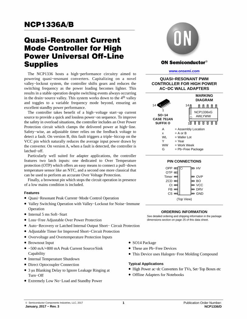
PIN FUNCTION DESCRIPTION
Pin No. Pin Name Function Pin Description
1 OPP Adjust the Over PowerProtection
A negative voltage applied to this pin reduces the internal maximum peakcurrent setpoint. Connecting it to an auxiliary winding through a resistordivider thus performs Over Power compensation. If grounded, OPP is null.
2 OTP Over−TemperatureProtection
Connect an NTC between this pin and GND pin. Pin 2 features an internalcurrent source that biases the NTC. When the NTC pulls the pin down, thecircuit permanently latches−off.
3 Timer Timer Wiring a capacitor to ground helps selecting the timer duration.
4 ZCD Zero Crossing Detection Connected to the auxiliary winding, this pin detects the core reset event.
5 Ct Timing Capacitor A capacitor connected to this pin acts as the timing capacitor in foldbackmode.
6 FB Feedback Pin Hooking an optocoupler collector to this pin will allow regulation.
7 CS Current Sense This pin monitors the primary peak current.
8 GND − This pin is the controller ground.
9 DRV Driver Output This pin is the driver’s output to an external MOSFET.
10 VCC Supplies the Controller This pin is connected to an external auxiliary voltage.
11 BO Brownout This pin is the brownout input.
12 OVP Over−Voltage Protection By pulling this pin high, the controller can be permanently latched−off.
13 NC − This pin is omitted for improved creepage.
14 HV High−Voltage Input Connected to the bulk capacitor, this pin powers the internal current sourceto deliver a startup current.
OVERCURRENT PROTECTION ON NCP1336 VERSIONS
Auto−Recovery Overcurrent protection
LatchedOvercurrent protection
NCP1336 / A X
NCP1336 / B X
NCP1336A/B
www.onsemi.com3
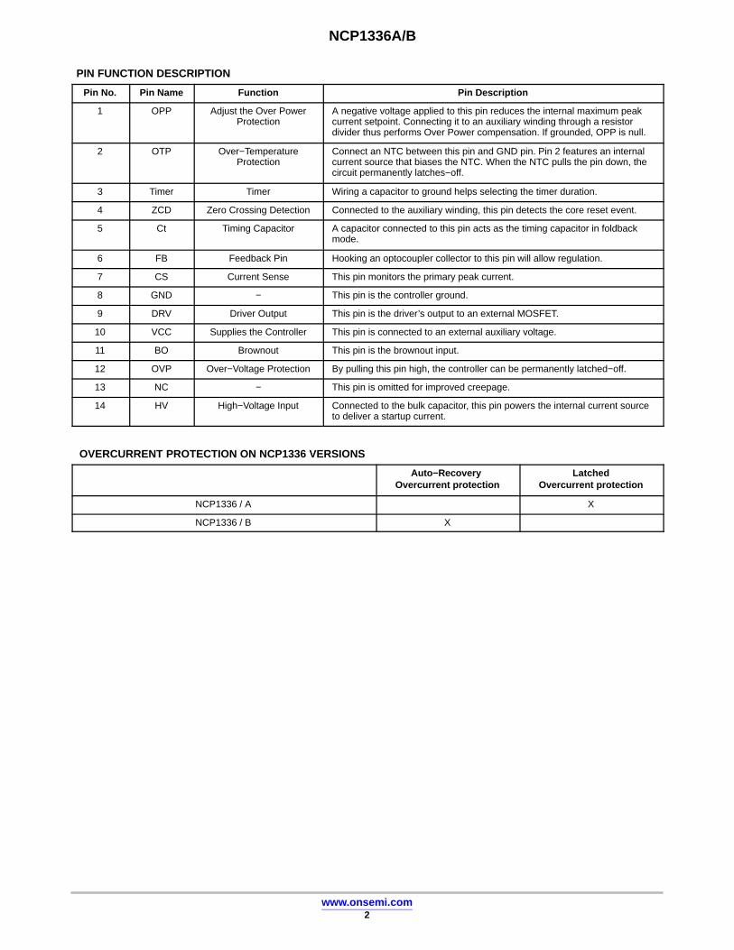
Figure 1. Typical Application Example
Vout
HV−bulk
GND
GND
NCP1336
OVPOTP
BO
OPP
ZCD
1
2
3
4
5
6
7
9
10
11
12
13
14
8
+
+
+Vin

NCP1336A/B
www.onsemi.com4
Figure 2. Internal Circuit Architecture
+
−
+
−
+
−
+
−
FB
Ct
ICt
1st
2nd
3rd
4th
VCO
+
−
+
−
ZCD
Laux
10 VESD
Vth
DRV leakage blanking
+
−
5us Timeout
100 ns
Decimal Counter
1
Demag
CLK
S
R
Q
CS
Rse
nse
LeadingEdge
Blanking+
−
Ilimit+ Vopp
/4
OPP +
−
IBO
Noise Delay
HV
VBO
+
−
+
−
VCC
T°
VOVP
VOTP
S
R
Q
noise delay
OTP
Timer
VDD
VDD
VDD
Soft−Start
+
−
ItimerC
Vdd
VCC
Aux
VCC ManagementLatch
VDD
HV
HV
HVStartup
Rpullup
rst
Fault
BO Reset
DRVGate
GrandReset
GrandReset
GrandReset
DRV
GND
Ipeak_min = 25% Limit
Clamp
Soft−Start End ? Then 1 Else 0
A & C:Latched
IpFlag
VDD
IOTP
OVP
+
Ilimit
+
−
+
−
SS End
SS End
ItimerD
S
R
Q
IpFlag
PWM Reset
PWMReset
2 3 4
Q
Q
Q
CtSetpoint
DischargeCt
PNOK
TSD
+
BO Reset
BO
LOVP reset
NCP1336A/B
www.onsemi.com5
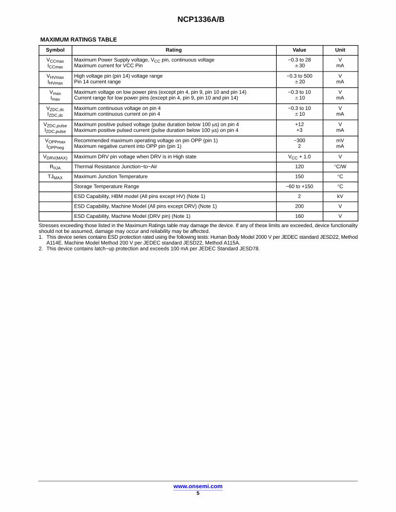
MAXIMUM RATINGS TABLE
Symbol Rating Value Unit
VCCmaxICCmax
Maximum Power Supply voltage, VCC pin, continuous voltageMaximum current for VCC Pin
−0.3 to 28�30
VmA
VHVmaxIHVmax
High voltage pin (pin 14) voltage rangePin 14 current range
−0.3 to 500�20
VmA
VmaxImax
Maximum voltage on low power pins (except pin 4, pin 9, pin 10 and pin 14)Current range for low power pins (except pin 4, pin 9, pin 10 and pin 14)
−0.3 to 10�10
VmA
VZDC,dcIZDC,dc
Maximum continuous voltage on pin 4Maximum continuous current on pin 4
−0.3 to 10�10
VmA
VZDC,pulseIZDC,pulse
Maximum positive pulsed voltage (pulse duration below 100 �s) on pin 4Maximum positive pulsed current (pulse duration below 100 �s) on pin 4
+12+3
VmA
VOPPmaxIOPPneg
Recommended maximum operating voltage on pin OPP (pin 1)Maximum negative current into OPP pin (pin 1)
−3002
mVmA
VDRV(MAX) Maximum DRV pin voltage when DRV is in High state VCC + 1.0 V
R�JA Thermal Resistance Junction−to−Air 120 °C/W
TJMAX Maximum Junction Temperature 150 °C
Storage Temperature Range −60 to +150 °C
ESD Capability, HBM model (All pins except HV) (Note 1) 2 kV
ESD Capability, Machine Model (All pins except DRV) (Note 1) 200 V
ESD Capability, Machine Model (DRV pin) (Note 1) 160 V
Stresses exceeding those listed in the Maximum Ratings table may damage the device. If any of these limits are exceeded, device functionalityshould not be assumed, damage may occur and reliability may be affected.1. This device series contains ESD protection rated using the following tests: Human Body Model 2000 V per JEDEC standard JESD22, Method
A114E. Machine Model Method 200 V per JEDEC standard JESD22, Method A115A.2. This device contains latch−up protection and exceeds 100 mA per JEDEC Standard JESD78.

NCP1336A/B
www.onsemi.com6
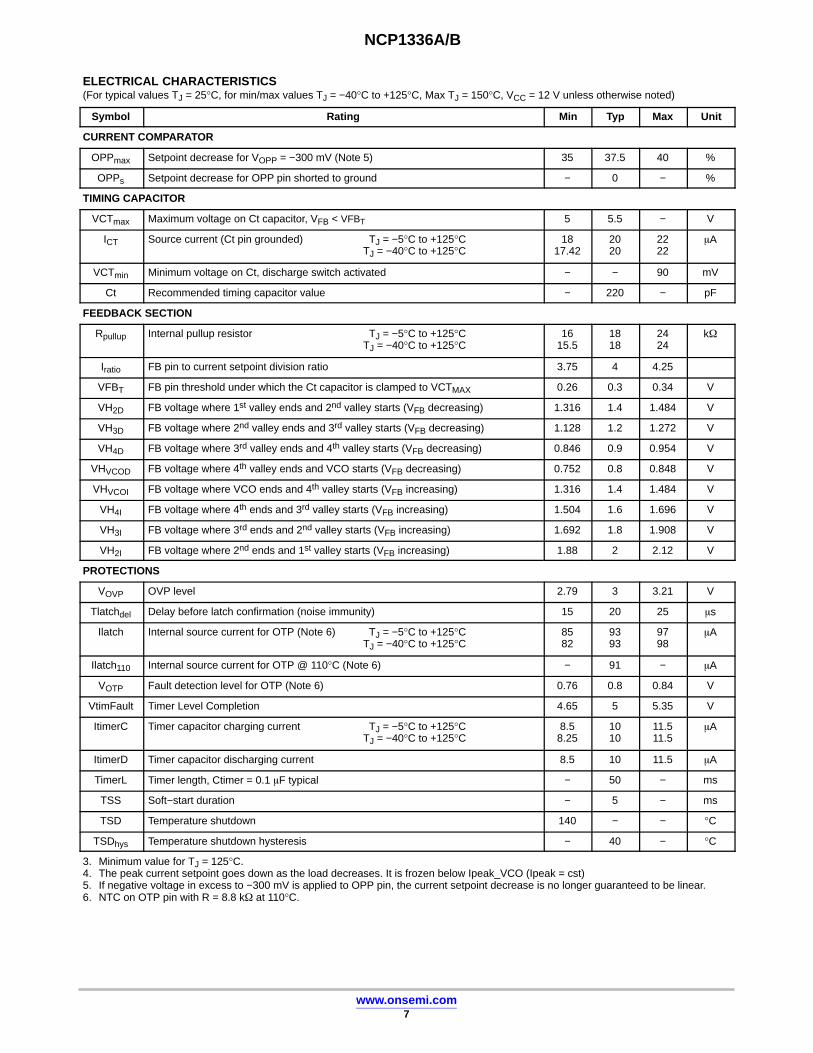
ELECTRICAL CHARACTERISTICS(For typical values TJ = 25°C, for min/max values TJ = −40°C to +125°C, Max TJ = 150°C, VCC = 12 V unless otherwise noted)
Symbol Rating Min Typ Max Unit
SUPPLY SECTION
VCCon VCC increasing level at which the current source turns−off 14 15 16 V
VCCmin VCC level below which output pulses are stopped 8 9 10 V
VCCreset Internal latch reset level − 5.5 − V
ICC1 Internal IC consumption, no output load on DRV pin (Fsw = 10 kHz) − 1.4 2.0 mA
ICC1light ICC1 for a Feedback Voltage Equal to VHVCO (internal bias reduction), with CT =220 pF (corresponding to an Fsw of about 20 kHz)
1.8 mA
ICC2 Internal IC consumption, 1 nF output load on pin 9, Fsw = 65 kHz − 2.5 3.0 mA
ICC3 Internal IC consumption, hiccup phase (VCCmin < VCC < VCCon) − 0.45 0.6 mA
INTERNAL STARTUP CURRENT SOURCE (TJ > 0�C) (HV Pin Biased to 60 Vdc)
IC2 High−voltage current source, VCC = 10 V (Note 3) 3 6 9 mA
IC1 High−voltage current source, VCC = 0 150 300 550 �A
VTh VCC transition level for IC1 to IC2 toggling point (IHV = 2.5 mA) 0.3 0.7 0.9 V
Ileak Leakage current for the high voltage source, VHV(pin) = 500 Vdc 1 12 30 �A
DRIVE OUTPUT
Tr Output voltage rise−time @ CL = 1 nF, 10%−90% of a 12 V output signal − 40 75 ns
Tf Output voltage fall−time @ CL = 1 nF, 10%−90% of a 12 V output signal − 25 60 ns
Isource Source current capability at VDRV = 2 V − 500 − mA
Isink Sink current capability at VDRV = 10 V − 800 − mA
VDRVlow DRV pin level at VCC close to VCCmin with a 33 k� resistor to GND and a 1 nFcapacitor to GND
7.6 − − V
VDRVhigh DRV pin level at VCC = 28 V with a 1 nF capacitor to GND (Note 3) − − 17 V
DEMAGNETIZATION INPUT
Vth Input threshold voltage (VZCD(pin) decreasing) 35 55 90 mV
VH Hysteresis (VZCD(pin) increasing) 15 35 55 mV
VCHVCL
Input clamp voltageHigh state (IZCD(pin) = 3.0 mA)Low state (IZCD(pin) = −2.0 mA)
8−0.9
10−0.7
120
VV
Tdem Demag propagation delay (VZCD(pin) decreasing from 4 V to −0.3 V) − 150 250 ns
Cpar Internal input capacitance at VZCD(pin) = 1 V − 10 − pF
Tblank Blanking Delay after tON 2 3 4 �s
Tout Timeout after last demag transition 4 5.25 6.5 �s
CURRENT COMPARATOR
IIB Input Bias Current @ 1 V input level on CS pin − 0.02 − �A
ILimit1 Maximum internal current setpoint – TJ = 25°C – OPP pin grounded 0.76 0.8 0.84 V
ILimit2 Maximum internal current setpoint – TJ from −40°C to 125°C – OPP pin grounded 0.744 0.8 0.856 V
Ipeak_VCO Percentage of maximum peak current level at which VCO takes over (Note 4) 22 25 28 %
TDEL Propagation delay from current detection to gate OFF state − 100 160 ns
TLEB Leading Edge Blanking Duration TJ = −5°C to +125°CTJ = −40°C to +125°C
240240
295295
350360
ns
3. Minimum value for TJ = 125°C.4. The peak current setpoint goes down as the load decreases. It is frozen below Ipeak_VCO (Ipeak = cst)5. If negative voltage in excess to −300 mV is applied to OPP pin, the current setpoint decrease is no longer guaranteed to be linear.6. NTC on OTP pin with R = 8.8 k� at 110°C.
NCP1336A/B
www.onsemi.com7
ELECTRICAL CHARACTERISTICS(For typical values TJ = 25°C, for min/max values TJ = −40°C to +125°C, Max TJ = 150°C, VCC = 12 V unless otherwise noted)
Symbol UnitMaxTypMinRating
CURRENT COMPARATOR
OPPmax Setpoint decrease for VOPP = −300 mV (Note 5) 35 37.5 40 %
OPPs Setpoint decrease for OPP pin shorted to ground − 0 − %
TIMING CAPACITOR
VCTmax Maximum voltage on Ct capacitor, VFB < VFBT 5 5.5 − V
ICT Source current (Ct pin grounded) TJ = −5°C to +125°CTJ = −40°C to +125°C
1817.42
2020
2222
�A
VCTmin Minimum voltage on Ct, discharge switch activated − − 90 mV
Ct Recommended timing capacitor value − 220 − pF
FEEDBACK SECTION
Rpullup Internal pullup resistor TJ = −5°C to +125°CTJ = −40°C to +125°C
1615.5
1818
2424
k�
Iratio FB pin to current setpoint division ratio 3.75 4 4.25
VFBT FB pin threshold under which the Ct capacitor is clamped to VCTMAX 0.26 0.3 0.34 V
VH2D FB voltage where 1st valley ends and 2nd valley starts (VFB decreasing) 1.316 1.4 1.484 V
VH3D FB voltage where 2nd valley ends and 3rd valley starts (VFB decreasing) 1.128 1.2 1.272 V
VH4D FB voltage where 3rd valley ends and 4th valley starts (VFB decreasing) 0.846 0.9 0.954 V
VHVCOD FB voltage where 4th valley ends and VCO starts (VFB decreasing) 0.752 0.8 0.848 V
VHVCOI FB voltage where VCO ends and 4th valley starts (VFB increasing) 1.316 1.4 1.484 V
VH4I FB voltage where 4th ends and 3rd valley starts (VFB increasing) 1.504 1.6 1.696 V
VH3I FB voltage where 3rd ends and 2nd valley starts (VFB increasing) 1.692 1.8 1.908 V
VH2I FB voltage where 2nd ends and 1st valley starts (VFB increasing) 1.88 2 2.12 V
PROTECTIONS
VOVP OVP level 2.79 3 3.21 V
Tlatchdel Delay before latch confirmation (noise immunity) 15 20 25 �s
Ilatch Internal source current for OTP (Note 6) TJ = −5°C to +125°CTJ = −40°C to +125°C
8582
9393
9798
�A
Ilatch110 Internal source current for OTP @ 110°C (Note 6) − 91 − �A
VOTP Fault detection level for OTP (Note 6) 0.76 0.8 0.84 V
VtimFault Timer Level Completion 4.65 5 5.35 V
ItimerC Timer capacitor charging current TJ = −5°C to +125°CTJ = −40°C to +125°C
8.58.25
1010
11.511.5
�A
ItimerD Timer capacitor discharging current 8.5 10 11.5 �A
TimerL Timer length, Ctimer = 0.1 �F typical − 50 − ms
TSS Soft−start duration − 5 − ms
TSD Temperature shutdown 140 − − °C
TSDhys Temperature shutdown hysteresis − 40 − °C
3. Minimum value for TJ = 125°C.4. The peak current setpoint goes down as the load decreases. It is frozen below Ipeak_VCO (Ipeak = cst)5. If negative voltage in excess to −300 mV is applied to OPP pin, the current setpoint decrease is no longer guaranteed to be linear.6. NTC on OTP pin with R = 8.8 k� at 110°C.

NCP1336A/B
www.onsemi.com8
ELECTRICAL CHARACTERISTICS(For typical values TJ = 25°C, for min/max values TJ = −40°C to +125°C, Max TJ = 150°C, VCC = 12 V unless otherwise noted)
Symbol UnitMaxTypMinRating
BROWNOUT PROTECTION
VBO Brownout level 0.744 0.8 0.856 V
IBO Hysteresis Current, VBO(pin) < VBO TJ = −5°C to +125°CTJ = −40°C to +125°C
98.65
1010
1111
�A
TBOdel Delay before BO confirmation (noise immunity) 11 17 23 �s
IBObias Brownout input bias current − 0.02 − �A
3. Minimum value for TJ = 125°C.4. The peak current setpoint goes down as the load decreases. It is frozen below Ipeak_VCO (Ipeak = cst)5. If negative voltage in excess to −300 mV is applied to OPP pin, the current setpoint decrease is no longer guaranteed to be linear.6. NTC on OTP pin with R = 8.8 k� at 110°C.

NCP1336A/B
www.onsemi.com9
APPLICATION INFORMATION
NCP1336 implements a standard current−modearchitecture operating in quasi−resonant mode. Thanks to anovel circuitry, the controller prevents valley−jumpinginstability and steadily locks out in selected valley as thepower demand goes down. Once the fourth valley is reached,the controller continues to reduce the frequency furtherdown, offering excellent efficiency over a wide operatingrange. Thanks to a fault timer combined to an OPP circuitry,the controller is able to efficiently limit the output power athigh−line.• Quasi−Resonance Current−mode operation:
implementing quasi−resonance operation in peakcurrent−mode control, the NCP1336 optimizes theefficiency by switching in the valley of the MOSFETdrain−source voltage. Thanks to a novel circuitry, thecontroller locks−out in a selected valley and remainslocked until the output loading significantly changes.This behavior is obtained by monitoring the feedbackvoltage. When the load becomes lighter, the feedbacksetpoint changes and the controller jumps into the nextvalley. It can go down to the 4th valley if necessary.Beyond this point, the controller reduces its switchingfrequency by freezing the peak current setpoint. Duringquasi−resonance operation, in case of very dampedvalleys, a 5 �s timer adds the missing valleys.
• Frequency reduction in light−load conditions: whenthe 4th valley is left, the controller reduces theswitching frequency which naturally improves thestandby power by a reduction of all switching losses.
• Overpower protection (OPP): a negative voltageapplied on OPP pin is directly added to the internalpeak current setpoint. If this voltage is created from anauxiliary winding with flyback polarity, a direct imageof the input voltage is subtracted from the internalclamp, thus reducing the peak current at high line. If theOPP pin is connected to ground no compensation isperformed.
• Internal high−voltage startup switch: reaching a lowno−load standby power represents a difficult exercisewhen the controller requires an external, lossy, resistorconnected to the bulk capacitor. Thanks to an internal
logic, the controller disables the high−voltage currentsource after startup which no longer hampers theconsumption in no−load situations.
• Internal soft−start: a soft−start precludes the mainpower switch from being stressed upon start−up. Itsduration is fixed and equal to 5 ms.
• OTP input: thanks to an internal current source, thecontroller allows the direct connection of an NTC toground. As soon as the pin is brought below VOTP bythe NTC, the circuit permanently latches−off. Duringsoft−start, the OTP comparator is masked to allow thevoltage on pin OTP to rise above VOTP.
• OVP input: thanks to an internal bias resistor toground, the controller allows the direct connection of azener diode (or a resistor divider for improvedaccuracy) to a monitored voltage. As soon as the pin isbrought above VOVP, the controller latches−off.
• Short−circuit protection: short−circuit and especiallyover−load protections are difficult to implement when astrong leakage inductance between auxiliary and powerwindings affects the transformer (where the auxiliarywinding level does not properly collapse in presence ofan output short). Here, when the internal 0.8 Vmaximum peak current limit is activated, the timercapacitor is charged. If the fault disappears, the timercapacitor is discharged by a current equal to thecharging current. If the timer reaches completion whilethe error flag is still present, the controller stops thepulses and goes into a latch−off phase, operating in alow−frequency burst−mode via a triple hiccupoperation. To limit the fault output power, adivide−by−three circuitry is installed on the VCC pinand requires 3 times a start−up sequence beforeattempting to restart on version B. As soon as the faultdisappears, the SMPS resumes operation. The latch−offphase can also be initiated, more classically, when VCCdrops below VCCmin. On version A, the fault is latched.
• Brownout: the NCP1336 includes a brownout circuitwhich safely stops the controller in case the inputvoltage is too low. Restart occurs via a complete startupsequence (latch reset and soft−start).
NCP1336A/B
www.onsemi.com10
APPLICATION INFORMATION
The NCP1336 has two operating modes: quasi resonantoperation and VCO operation.
The operating mode is fixed by the FB voltage:• Quasi−resonant operation occurs for FB voltage higher
than 0.8 V (FB decreasing) or higher than 1.6 V (FBincreasing) which correspond to high output power andmedium output power.During quasi−resonant operation, the operating valley(1st, 2nd, 3rd or 4th) is fixed by the FB voltage which iscompared internally to several voltage referencescorresponding to the different valleys. There is a widehysteresis on each valley, allowing the controller toadjust the output power by the current−mode controlwithout jumping between valleys. The peak current isvariable and is set by the FB voltage divided by 4.
• VCO operation occurs for FB voltage lower than 0.8 V(FB decreasing) or lower than 1.6 V (FB increasing).This corresponds to low output power.During VCO operation, the peak current is fixed to 25%
of its maximum value and the frequency is variable.The frequency is set by the end of charge of Ctcapacitor. This capacitor is charged with a constantcurrent source and the capacitor voltage is compared toan internal threshold fixed by FB voltage. When thiscapacitor voltage reaches the threshold the capacitor israpidly discharged down to 0 V and a new period start.
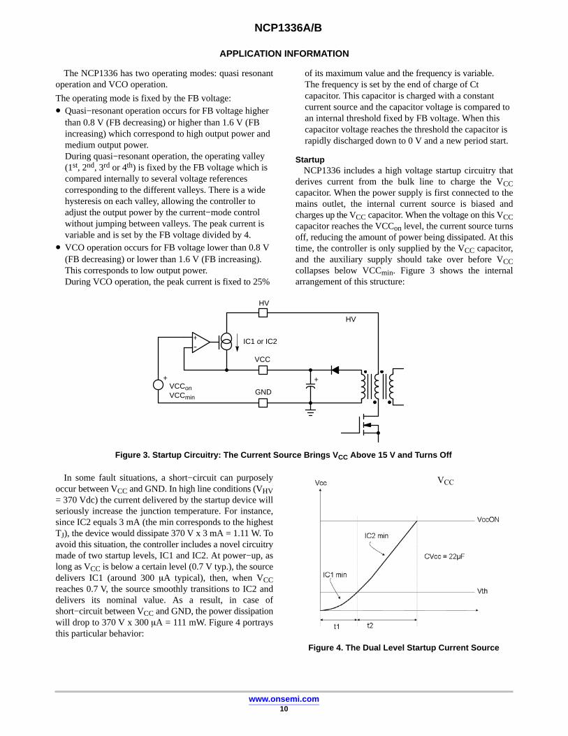
StartupNCP1336 includes a high voltage startup circuitry that
derives current from the bulk line to charge the VCCcapacitor. When the power supply is first connected to themains outlet, the internal current source is biased andcharges up the VCC capacitor. When the voltage on this VCCcapacitor reaches the VCCon level, the current source turnsoff, reducing the amount of power being dissipated. At thistime, the controller is only supplied by the VCC capacitor,and the auxiliary supply should take over before VCCcollapses below VCCmin. Figure 3 shows the internalarrangement of this structure:
Figure 3. Startup Circuitry: The Current Source Brings VCC Above 15 V and Turns Off
-+
+ +
HV
VCC
GND
IC1 or IC2
HV
VCConVCCmin
In some fault situations, a short−circuit can purposelyoccur between VCC and GND. In high line conditions (VHV= 370 Vdc) the current delivered by the startup device willseriously increase the junction temperature. For instance,since IC2 equals 3 mA (the min corresponds to the highestTJ), the device would dissipate 370 V x 3 mA = 1.11 W. Toavoid this situation, the controller includes a novel circuitrymade of two startup levels, IC1 and IC2. At power−up, aslong as VCC is below a certain level (0.7 V typ.), the sourcedelivers IC1 (around 300 �A typical), then, when VCCreaches 0.7 V, the source smoothly transitions to IC2 anddelivers its nominal value. As a result, in case ofshort−circuit between VCC and GND, the power dissipationwill drop to 370 V x 300 �A = 111 mW. Figure 4 portraysthis particular behavior:
Figure 4. The Dual Level Startup Current Source
VCC
NCP1336A/B
www.onsemi.com11
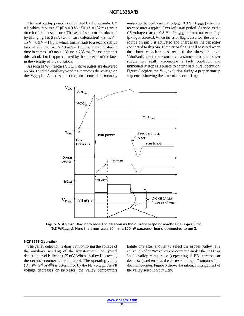
The first startup period is calculated by the formula, CV= It which implies a 22 �F x 0.9 V / 150 �A = 132 ms startuptime for the first sequence. The second sequence is obtainedby changing I to 3 mA (worst case calculation) with �V =15 V − 0.9 V = 14.1 V, which finally leads to a second startuptime of 22 �F x 14.1 V / 3 mA = 103 ms. The total startuptime becomes 103 ms + 132 ms = 235 ms. Please note thatthis calculation is approximated by the presence of the kneein the vicinity of the transition.
As soon as VCC reaches VCCon, drive pulses are deliveredon pin 9 and the auxiliary winding increases the voltage onthe VCC pin. At the same time, the controller smoothly
ramps up the peak current to Imax (0.8 V / Rsense) which isreached after a typical 5 ms soft−start period. As soon as theCS voltage reaches 0.8 V = ILimit1, the internal error flagIpFlag is asserted. When the error flag is asserted, the currentsource on pin 3 is activated and charges up the capacitorconnected to this pin. If the error flag is still asserted whenthe timer capacitor has reached the threshold levelVtimFault, then the controller assumes that the powersupply has really undergone a fault condition andimmediately stops all pulses to enter a safe burst operation.Figure 5 depicts the VCC evolution during a proper startupsequence, showing the state of the error flag:
Figure 5. An error flag gets asserted as soon as the current setpoint reaches its upper limit (0.8 V/Rsense). Here the timer lasts 50 ms, a 100 nF capacitor being connected to pin 3.
NCP1336 OperationThe valley detection is done by monitoring the voltage of
the auxiliary winding of the transformer. The typicaldetection level is fixed at 55 mV. When a valley is detected,the decimal counter is incremented. The operating valley(1st, 2nd, 3rd or 4th) is determined by the FB voltage. As FBvoltage decreases or increases, the valley comparators
toggle one after another to select the proper valley. Theactivation of an “n” valley comparator disables the “n+1” or“n−1” valley comparator (depending if FB increases ordecreases) and enables the corresponding “n” output of thedecimal counter. Figure 6 shows the internal arrangement ofthe valley selection circuitry.
NCP1336A/B
www.onsemi.com12
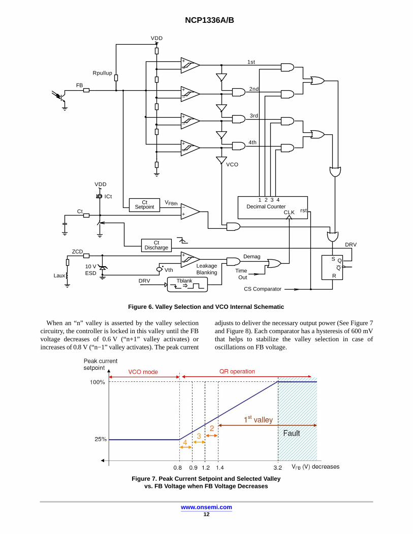
Figure 6. Valley Selection and VCO Internal Schematic
+−
+−
+−
+−
FB
Ct
ICt
1st
2nd
3rd
4th
VCO
+−
+−
ZCD
Laux
10 VESD
Vth
DRV Tblank
Decimal Counter1
Demag
CLK
S
R
QLeakageBlanking
VDD
VDD
Rpullup
rst
DRV
2 3 4
Q
CtSetpoint
DischargeCt
CS Comparator
TimeOut
VFBth
When an “n” valley is asserted by the valley selectioncircuitry, the controller is locked in this valley until the FBvoltage decreases of 0.6 V (“n+1” valley activates) orincreases of 0.8 V (“n−1” valley activates). The peak current
adjusts to deliver the necessary output power (See Figure 7and Figure 8). Each comparator has a hysteresis of 600 mVthat helps to stabilize the valley selection in case ofoscillations on FB voltage.
Figure 7. Peak Current Setpoint and Selected Valleyvs. FB Voltage when FB Voltage Decreases
NCP1336A/B
www.onsemi.com13
Figure 8. Selected Valley According to FB State
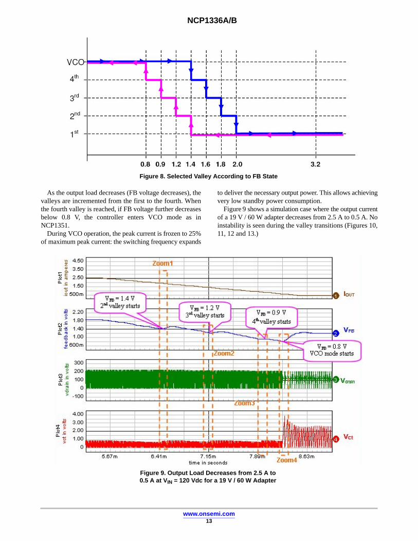
As the output load decreases (FB voltage decreases), thevalleys are incremented from the first to the fourth. Whenthe fourth valley is reached, if FB voltage further decreasesbelow 0.8 V, the controller enters VCO mode as inNCP1351.
During VCO operation, the peak current is frozen to 25%of maximum peak current: the switching frequency expands
to deliver the necessary output power. This allows achievingvery low standby power consumption.
Figure 9 shows a simulation case where the output currentof a 19 V / 60 W adapter decreases from 2.5 A to 0.5 A. Noinstability is seen during the valley transitions (Figures 10,11, 12 and 13.)
Figure 9. Output Load Decreases from 2.5 A to0.5 A at VIN = 120 Vdc for a 19 V / 60 W Adapter

NCP1336A/B
www.onsemi.com14
Figure 10. Zoom 1: 1st to 2nd Valley Transition
Figure 11. Zoom 2: 2nd to 3rd Valley Transition
2 feedback 3 vdrain 4 vct
600m
1.00
1.40
1.80
2.20
feed
back
in v
olts
Plo
t2
2
−100
0
100
200
300
vdra
in in
vol
tsP
lot3
3
6.41m 6.43m 6.45m 6.47m 6.49mtime in seconds
0
1.00
2.00
3.00
4.00
vct i
n vo
ltsP
lot4
4
Vdrain
VFB
VCt
2 feedback 3 vdrain 4 vct
600m
1.00
1.40
1.80
2.20
feed
back
in v
olts
Plo
t2
2
−100
0
100
200
300
vdra
in in
vol
tsP
lot3
3
7.135m 7.153m 7.170m 7.188m 7.205mtime in seconds
0
1.00
2.00
3.00
4.00
vct i
n vo
ltsP
lot4
4
Vdrain
VFB
VCt

NCP1336A/B
www.onsemi.com15
Figure 12. Zoom 3: 3rd to 4th Valley Transition
Figure 13. Zoom 4: 4th Valley to VCO Mode Transistion
2 feedback 3 vdrain 4 vct
600m
1.00
1.40
1.80
2.20
feed
back
in v
olts
Plo
t2
2
−100
0
100
200
300
vdra
in in
vol
tsP
lot3
3
7.902m 7.917m 7.932m 7.946m 7.961mtime in seconds
0
1.00
2.00
3.00
4.00
vct i
n vo
ltsP
lot4
4
Vdrain
VFB
VCt
2 feedback 3 vdrain 4 vct
600m
1.00
1.40
1.80
2.20
feed
back
in v
olts
Plo
t2
2
−100
0
100
200
300
vdra
in in
vol
tsP
lot3 3
8.24m 8.26m 8.29m 8.31m 8.34mtime in seconds
0
1.00
2.00
3.00
4.00
vct i
n vo
ltsP
lot4
4
Vdrain
VFB
VCt
NCP1336A/B
www.onsemi.com16
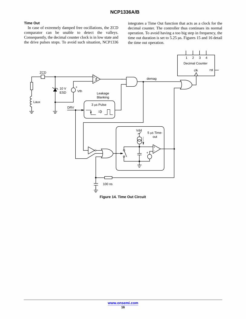
Time OutIn case of extremely damped free oscillations, the ZCD
comparator can be unable to detect the valleys.Consequently, the decimal counter clock is in low state andthe drive pulses stops. To avoid such situation, NCP1336
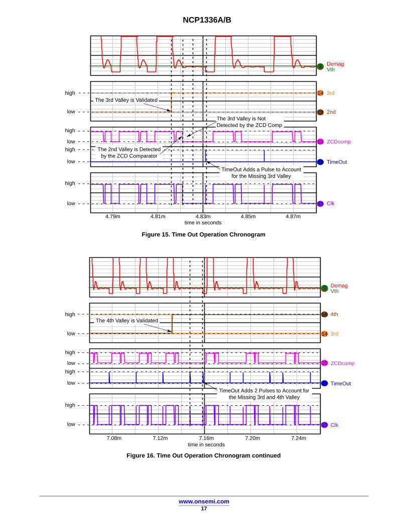
integrates a Time Out function that acts as a clock for thedecimal counter. The controller thus continues its normaloperation. To avoid having a too big step in frequency, thetime out duration is set to 5.25 �s. Figures 15 and 16 detailthe time out operation.
Figure 14. Time Out Circuit
-+
+10 VESD
ZCD
Laux
Vth
3 �s PulseDRV
rst
demag
Decimal Counter
clk
4321
LeakageBlanking
-+
+
Vdd5 �s Time-
out
100 ns
NCP1336A/B
www.onsemi.com17
43
14
12
15
16
4.79m 4.81m 4.83m 4.85m 4.87mtime in seconds
17
43
14
18
15
16
7.08m 7.12m 7.16m 7.20m 7.24mtime in seconds
17
Figure 15. Time Out Operation Chronogram
Figure 16. Time Out Operation Chronogram continued
high
low
high
low
high
low
high
low
high
low
high
low
high
low
high
low
The 3rd Valley is Validated
The 3rd Valley is NotDetected by the ZCD Comp
TimeOut Adds a Pulse to Accountfor the Missing 3rd Valley
The 2nd Valley is Detectedby the ZCD Comparator
The 4th Valley is Validated
TimeOut Adds 2 Pulses to Account forthe Missing 3rd and 4th Valley
DemagVth
3rd
2nd
ZCDcomp
TimeOut
Clk
DemagVth
3rd
4th
ZCDcomp
TimeOut
Clk
NCP1336A/B
www.onsemi.com18
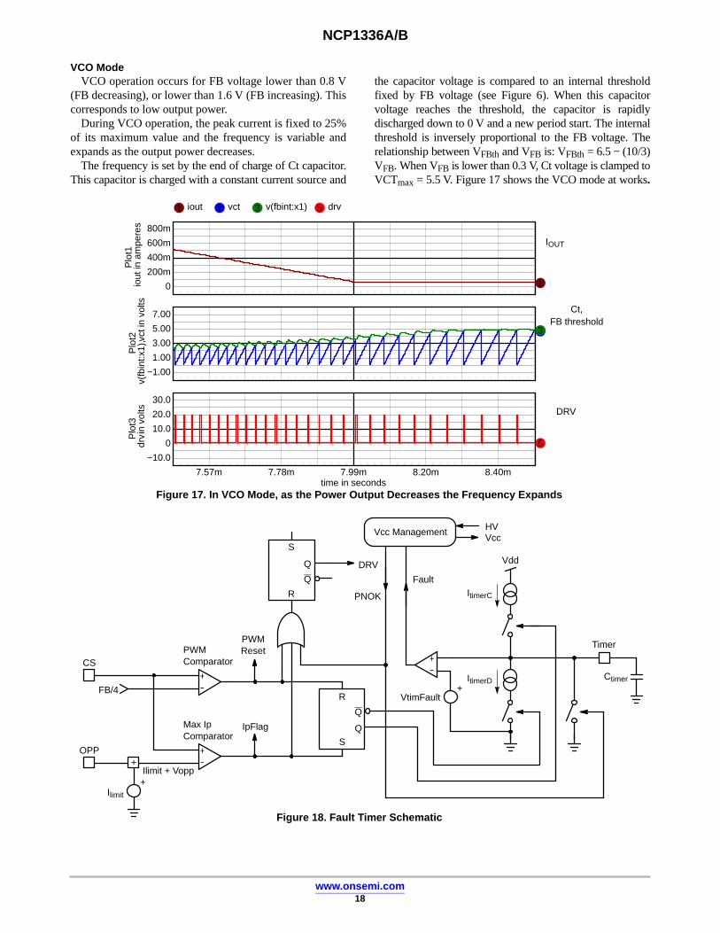
VCO ModeVCO operation occurs for FB voltage lower than 0.8 V
(FB decreasing), or lower than 1.6 V (FB increasing). Thiscorresponds to low output power.
During VCO operation, the peak current is fixed to 25%of its maximum value and the frequency is variable andexpands as the output power decreases.
The frequency is set by the end of charge of Ct capacitor.This capacitor is charged with a constant current source and
the capacitor voltage is compared to an internal thresholdfixed by FB voltage (see Figure 6). When this capacitorvoltage reaches the threshold, the capacitor is rapidlydischarged down to 0 V and a new period start. The internalthreshold is inversely proportional to the FB voltage. Therelationship between VFBth and VFB is: VFBth = 6.5 − (10/3)VFB. When VFB is lower than 0.3 V, Ct voltage is clamped toVCTmax = 5.5 V. Figure 17 shows the VCO mode at works.
1 iout 2 vct 3 v(fbint:x1) 5 drv
0
200m
400m
600m
800m
iout
in a
mpe
res
Plo
t1
1
−1.00
1.00
3.00
5.00
7.00
v(fb
int:x
1),v
ct in
vol
tsP
lot2 23
7.57m 7.78m 7.99m 8.20m 8.40mtime in seconds
−10.0
0
10.0
20.0
30.0
drv i
n vo
ltsP
lot3
5
DRV
Ct,FB threshold
IOUT
Figure 17. In VCO Mode, as the Power Output Decreases the Frequency Expands
Figure 18. Fault Timer Schematic
-+
-+
Ilimit
+
ItimerC
Timer
Vdd
OPP
CS
FB/4
PWMComparator
Max IpComparator
Ilimit + Vopp
R
S
Q
Q
R
S
Q
Q
+-
DRV
IpFlag
PWMReset
Vcc Management
CtimerItimerD
PNOK
Fault
HVVcc
VtimFault+
+

NCP1336A/B
www.onsemi.com19
Short−circuit or Overload ModeFigure 18 shows the implementation of the fault timer.When the current in the MOSFET is higher than, “Max
(0.8 V / Rsense) Ip” comparator trips and the timer capacitor ischarged by ItimerC current source. When the current comesback within safe limits, “Max Ip” comparator becomes silent
and the PWM comparator triggers the discharge of the timercapacitor.
If “IpFlag” and PWMreset occur at the same time, thePWMreset signal is the strongest and the capacitor isdischarged.
3 v(ipflag:x1) 4 v(pwm:x1) 8 feedback 9 vtimer
−200m
200m
600m
1.00
1.40
vtim
er in
vol
ts
1.80
2.20
2.60
3.00
3.40
feed
back
in v
olts
plot
1
89
6.13m 6.37m 6.60m 6.84m 7.08mtime in seconds
plot
2
4
3
IpFlag
PWMreset
VTimer
VFB
low
highlow
high
Figure 19. Timer Operating Chronograms
There can be various events that force a fault on theprimary side controller. We can split them in differentsituation, each having a particular configuration:
1. The converter regulates but the auxiliary windingcollapses: this is a typical situation linked to theusage of a constant−current / constant−voltage(CC−CV) type of controller. If the output currentincreases, the voltage feedback loop gives up andthe current loop takes over. It means that VOUTgoes low but the feedback loop is still closedbecause of the output current monitoring.Therefore, seen from the primary side, there is nofault. However, there are numerous chargerapplications where the output voltage shall not gobelow a certain limit, even if the current iscontrolled. To cope with this situation, thecontroller features a precise under−voltage lockoutcomparator biased to a VCCmin level. When thislevel is crossed, whatever the other pin conditions,pulses are stopped and the controller enters thesafe hiccup mode, trying to re−start. Figure 20shows how the converter will behave in this
situation. If the fault goes away, the SMPSresumes operation.
2. In the second case, the converter operates inregulation, but the output is severely overloaded.However, due to the bad coupling between thepower and the auxiliary windings, the controllerVCC does not go low. The peak current is pushedto the maximum, the error flag IpFlag isconsequently asserted and the timer starts to count.Upon completion, all pulses are stopped andtriple−startup hiccup mode is entered forversion B. If the fault goes away, the SMPSresumes operation (Figure 21). For version A,when the timer finishes counting, the pulses stopand the circuit stays latched until the user cyclesdown the power supply (Figure 22).
3. Another case exists where the short−circuit makesthe auxiliary level go below VCCmin. In that case,the timer length is truncated and all pulses arestopped. The triple hiccup fault mode is enteredand the SMPS tries to re−start. When the fault isremoved, the SMPS resumes operation.

NCP1336A/B
www.onsemi.com20
Figure 20. First Fault Mode Case, the AuxiliaryWinding Collapses but Feedback is Still There
Figure 21. Short−Circuit Case Where Vaux DoesNOT Collapse on Version B
Figure 22. Short−Circuit Case Where Vaux DoesNOT Collapse on Version A
NCP1336A/B
www.onsemi.com21
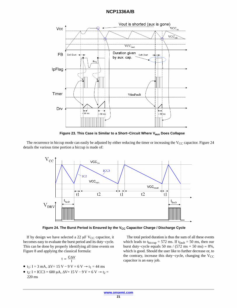
Figure 23. This Case is Similar to a Short−Circuit Where Vaux Does Collapse
The recurrence in hiccup mode can easily be adjusted by either reducing the timer or increasing the VCC capacitor. Figure 24details the various time portion a hiccup is made of:
Figure 24. The Burst Period is Ensured by the VCC Capacitor Charge / Discharge Cycle
If by design we have selected a 22 �F VCC capacitor, itbecomes easy to evaluate the burst period and its duty−cycle.This can be done by properly identifying all time events onFigure 8 and applying the classical formula:
t � C�VI
• t1: I = 3 mA, ΔV= 15 V − 9 V = 6 V � t1 = 44 ms
• t2: I = ICC3 = 600 �A, ΔV= 15 V − 9 V = 6 V � t2 =220 ms
The total period duration is thus the sum of all these eventswhich leads to thiccup = 572 ms. If tfault = 50 ms, then ourburst duty−cycle equals 50 ms / (572 ms + 50 ms) ≈ 8%,which is good. Should the user like to further decrease or, tothe contrary, increase this duty−cycle, changing the VCCcapacitor is an easy job.

NCP1336A/B
www.onsemi.com22
Over Voltage / Over Temperature ProtectionThe OTP and OVP pins feature circuitries to protect the circuit against high temperature and high voltage (see Figure 25).
Figure 25. Pin Latch Circuitry
OVP
IOTP
VOTP+
20 �s Filter
-+
-+
VOVP+
Rbias
End of Soft−start
OTP
Vdd
Vcc
T°
OTPA current flows out of the OTP pin into the NTC resistor,
thus imposing a voltage on the OTP pin. When thetemperature increases, the NTC’s resistance reduces (Forexample, at 110°C, RNTC = 8.8 k instead of 470 k at 25°C)and the voltage on the OTP pin decreases until it reachesVOTP: the comparator trips and latches−off the controller. Toreset the controller, the user must unplug and re−plug thepower supply.
During start−up and soft−start, the output of the OTPcomparator is masked to allow for the voltage on the OTPpin to grow if a capacitor is installed across the NTC forfiltering purposes.
OVPWhen VCC increases (OVP), a current starts to flow in the
zener (which much be biased externally), and the voltage onthe OVP pin starts to increase. When this voltage reachesVOVP, the circuit immediately stops pulsing and stayslatched until the user cycles down the power supply. Thereset occurs if VCC drops below 5 V (or brownout isdetected).
Figures 26 and 27 details the operating diagrams in caseof an over temperature and an overvoltage event.
Figure 26. Operating Diagrams in Case of an Over Temperature
VOTP(pin) Ambient temperatureincreases
VOTP
NCP1336A/B
www.onsemi.com23
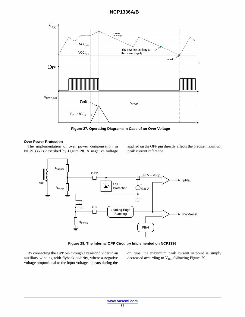
Figure 27. Operating Diagrams in Case of an Over Voltage
VOVP(pin)
VOVP
Over Power ProtectionThe implementation of over power compensation in
NCP1336 is described by Figure 28. A negative voltageapplied on the OPP pin directly affects the precise maximumpeak current reference.
Figure 28. The Internal OPP Circuitry Implemented on NCP1336
+-
Rupper
Rlower
OPP
0.8 V+
Aux
CSLeading Edge
Blanking
FB/4
-+
+
ESDProtection
0.8 V + Vopp
IpFlag
PWMreset
Rsense
By connecting the OPP pin through a resistor divider to anauxiliary winding with flyback polarity, where a negativevoltage proportional to the input voltage appears during the
on−time, the maximum peak current setpoint is simplydecreased according to VIN, following Figure 29.
NCP1336A/B
www.onsemi.com24
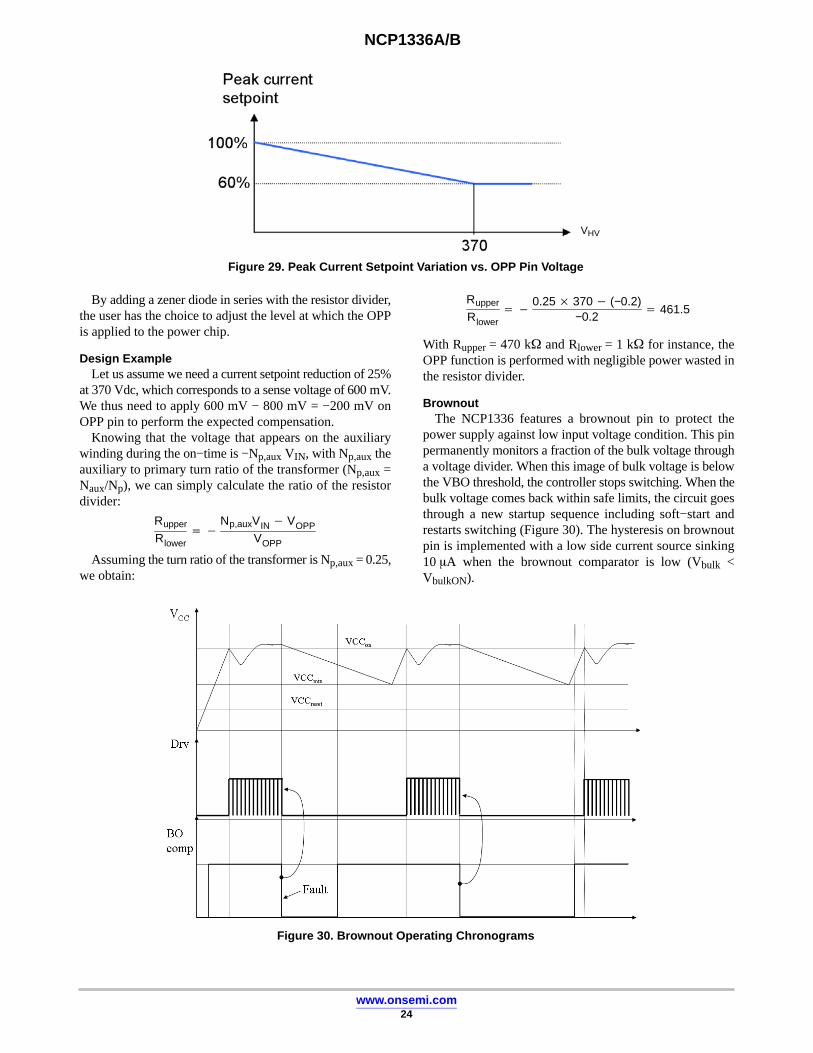
Figure 29. Peak Current Setpoint Variation vs. OPP Pin Voltage
VHV
By adding a zener diode in series with the resistor divider,the user has the choice to adjust the level at which the OPPis applied to the power chip.
Design ExampleLet us assume we need a current setpoint reduction of 25%
at 370 Vdc, which corresponds to a sense voltage of 600 mV.We thus need to apply 600 mV − 800 mV = −200 mV onOPP pin to perform the expected compensation.
Knowing that the voltage that appears on the auxiliarywinding during the on−time is −Np,aux VIN, with Np,aux theauxiliary to primary turn ratio of the transformer (Np,aux =Naux/Np), we can simply calculate the ratio of the resistordivider:
Rupper
Rlower� �
Np,auxVIN � VOPPVOPP
Assuming the turn ratio of the transformer is Np,aux = 0.25,we obtain:
Rupper
Rlower� �
0.25 � 370 � (−0.2)−0.2
� 461.5
With Rupper = 470 k� and Rlower = 1 k� for instance, theOPP function is performed with negligible power wasted inthe resistor divider.
BrownoutThe NCP1336 features a brownout pin to protect the
power supply against low input voltage condition. This pinpermanently monitors a fraction of the bulk voltage througha voltage divider. When this image of bulk voltage is belowthe VBO threshold, the controller stops switching. When thebulk voltage comes back within safe limits, the circuit goesthrough a new startup sequence including soft−start andrestarts switching (Figure 30). The hysteresis on brownoutpin is implemented with a low side current source sinking10 �A when the brownout comparator is low (Vbulk <VbulkON).
Figure 30. Brownout Operating Chronograms
NCP1336A/B
www.onsemi.com25
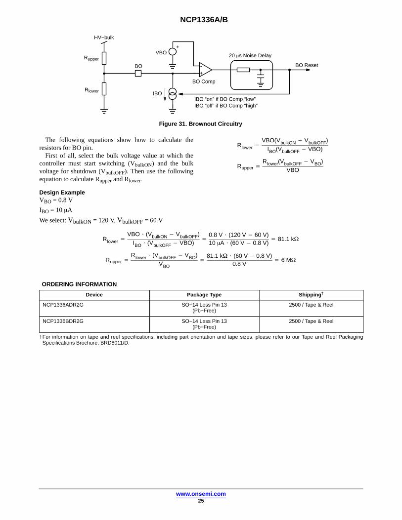
Figure 31. Brownout Circuitry
+-
HV−bulk
Rupper
Rlower
BO
IBO
VBO+
BO Comp
BO Reset
20 �s Noise Delay
IBO “on” if BO Comp “low”IBO “off” if BO Comp “high”
The following equations show how to calculate theresistors for BO pin.
First of all, select the bulk voltage value at which thecontroller must start switching (VbulkON) and the bulkvoltage for shutdown (VbulkOFF). Then use the followingequation to calculate Rupper and Rlower.
Rlower �VBO(VbulkON � VbulkOFF)
IBO(VbulkOFF � VBO)
Rupper �Rlower(VbulkOFF � VBO)
VBO
Design ExampleVBO = 0.8 V
IBO = 10 �A
We select: VbulkON = 120 V, VbulkOFF = 60 V
Rlower �VBO � (VbulkON � VbulkOFF)
IBO � (VbulkOFF � VBO)�
0.8 V � (120 V � 60 V)10 �A � (60 V � 0.8 V)
� 81.1 k�
Rupper �Rlower � (VbulkOFF � VBO)
VBO�
81.1 k� � (60 V � 0.8 V)0.8 V
� 6 M�
ORDERING INFORMATION
Device Package Type Shipping†
NCP1336ADR2G SO−14 Less Pin 13(Pb−Free)
2500 / Tape & Reel
NCP1336BDR2G SO−14 Less Pin 13(Pb−Free)
2500 / Tape & Reel
†For information on tape and reel specifications, including part orientation and tape sizes, please refer to our Tape and Reel PackagingSpecifications Brochure, BRD8011/D.
NCP1336A/B
www.onsemi.com26
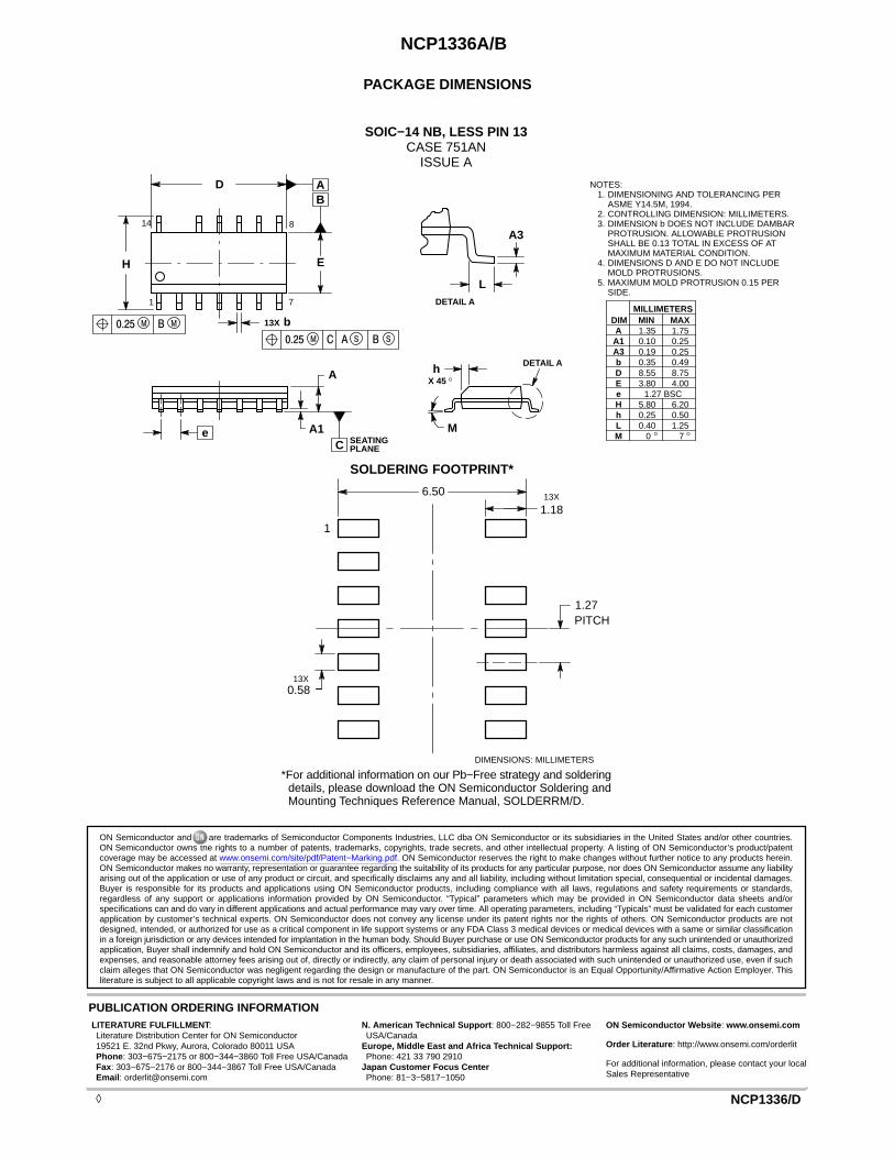
PACKAGE DIMENSIONS
SOIC−14 NB, LESS PIN 13CASE 751AN
ISSUE A
NOTES:1. DIMENSIONING AND TOLERANCING PER
ASME Y14.5M, 1994.2. CONTROLLING DIMENSION: MILLIMETERS.3. DIMENSION b DOES NOT INCLUDE DAMBAR
PROTRUSION. ALLOWABLE PROTRUSIONSHALL BE 0.13 TOTAL IN EXCESS OF ATMAXIMUM MATERIAL CONDITION.
4. DIMENSIONS D AND E DO NOT INCLUDEMOLD PROTRUSIONS.
5. MAXIMUM MOLD PROTRUSION 0.15 PERSIDE.
H
14 8
71
M0.25 B M
C
hX 45
SEATINGPLANE
A1
A
M
�
DIM MIN MAXMILLIMETERS
D 8.55 8.75E 3.80 4.00
A 1.35 1.75
b 0.35 0.49
L 0.40 1.25
e 1.27 BSC
A3 0.19 0.25A1 0.10 0.25
M 0 7
H 5.80 6.20h 0.25 0.50
� �
6.50
13X0.58
13X
1.18
1.27
DIMENSIONS: MILLIMETERS
1
PITCH
SOLDERING FOOTPRINT*
*For additional information on our Pb−Free strategy and solderingdetails, please download the ON Semiconductor Soldering andMounting Techniques Reference Manual, SOLDERRM/D.
SAM0.25 B SC
b13X
BA
E
D
e
DETAIL A
L
A3
DETAIL A
ON Semiconductor and are trademarks of Semiconductor Components Industries, LLC dba ON Semiconductor or its subsidiaries in the United States and/or other countries.ON Semiconductor owns the rights to a number of patents, trademarks, copyrights, trade secrets, and other intellectual property. A listing of ON Semiconductor’s product/patentcoverage may be accessed at www.onsemi.com/site/pdf/Patent−Marking.pdf. ON Semiconductor reserves the right to make changes without further notice to any products herein.ON Semiconductor makes no warranty, representation or guarantee regarding the suitability of its products for any particular purpose, nor does ON Semiconductor assume any liabilityarising out of the application or use of any product or circuit, and specifically disclaims any and all liability, including without limitation special, consequential or incidental damages.Buyer is responsible for its products and applications using ON Semiconductor products, including compliance with all laws, regulations and safety requirements or standards,regardless of any support or applications information provided by ON Semiconductor. “Typical” parameters which may be provided in ON Semiconductor data sheets and/orspecifications can and do vary in different applications and actual performance may vary over time. All operating parameters, including “Typicals” must be validated for each customerapplication by customer’s technical experts. ON Semiconductor does not convey any license under its patent rights nor the rights of others. ON Semiconductor products are notdesigned, intended, or authorized for use as a critical component in life support systems or any FDA Class 3 medical devices or medical devices with a same or similar classificationin a foreign jurisdiction or any devices intended for implantation in the human body. Should Buyer purchase or use ON Semiconductor products for any such unintended or unauthorizedapplication, Buyer shall indemnify and hold ON Semiconductor and its officers, employees, subsidiaries, affiliates, and distributors harmless against all claims, costs, damages, andexpenses, and reasonable attorney fees arising out of, directly or indirectly, any claim of personal injury or death associated with such unintended or unauthorized use, even if suchclaim alleges that ON Semiconductor was negligent regarding the design or manufacture of the part. ON Semiconductor is an Equal Opportunity/Affirmative Action Employer. Thisliterature is subject to all applicable copyright laws and is not for resale in any manner.
PUBLICATION ORDERING INFORMATIONN. American Technical Support: 800−282−9855 Toll FreeUSA/Canada
Europe, Middle East and Africa Technical Support:Phone: 421 33 790 2910
Japan Customer Focus CenterPhone: 81−3−5817−1050
NCP1336/D
LITERATURE FULFILLMENT:Literature Distribution Center for ON Semiconductor19521 E. 32nd Pkwy, Aurora, Colorado 80011 USAPhone: 303−675−2175 or 800−344−3860 Toll Free USA/CanadaFax: 303−675−2176 or 800−344−3867 Toll Free USA/CanadaEmail: [email protected]
ON Semiconductor Website: www.onsemi.com
Order Literature: http://www.onsemi.com/orderlit
For additional information, please contact your localSales Representative
◊
Related Documents