Nanophysics Nanophysics Michael Hietschold Solid Surfaces Analysis Group & Electron Microscopy Laboratory Institute of Physics Portland State University, May 2005

Nanophysics Michael Hietschold Solid Surfaces Analysis Group & Electron Microscopy Laboratory Institute of Physics Portland State University, May 2005.
Dec 29, 2015
Welcome message from author
This document is posted to help you gain knowledge. Please leave a comment to let me know what you think about it! Share it to your friends and learn new things together.
Transcript

NanophysicsNanophysics
Michael Hietschold
Solid Surfaces Analysis Group &
Electron Microscopy Laboratory
Institute of Physics
Portland State University, May 2005
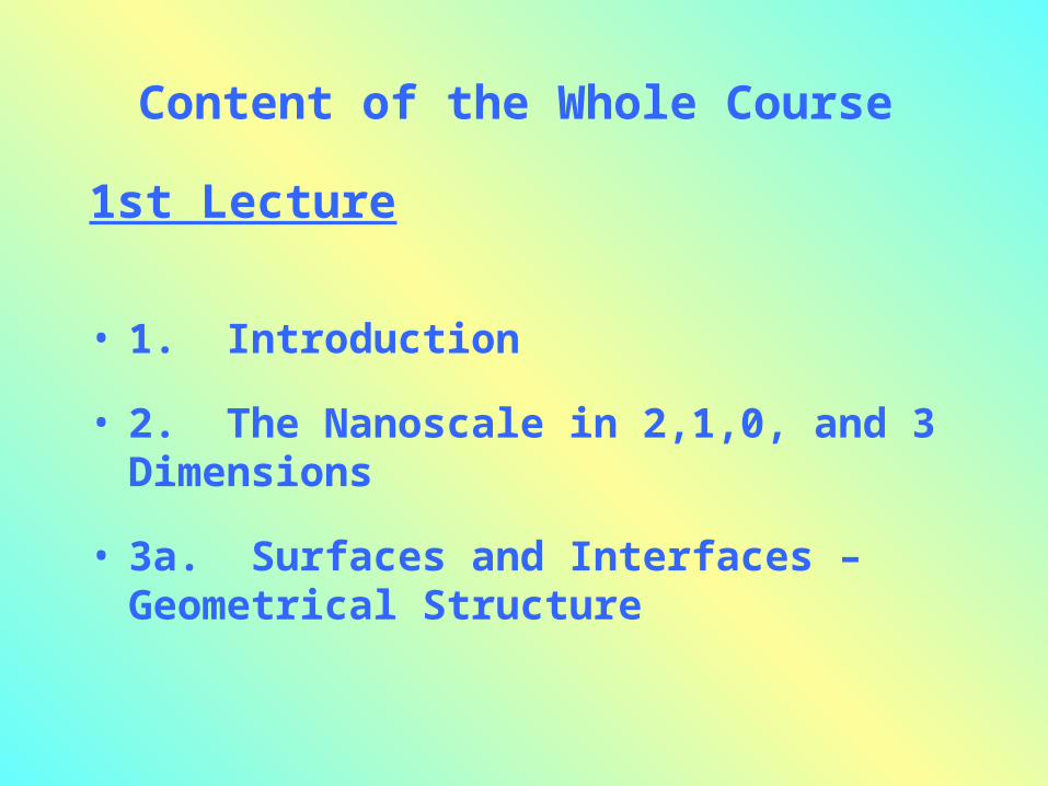
Content of the Whole Course
1st Lecture
• 1. Introduction
• 2. The Nanoscale in 2,1,0, and 3 Dimensions
• 3a. Surfaces and Interfaces – Geometrical Structure
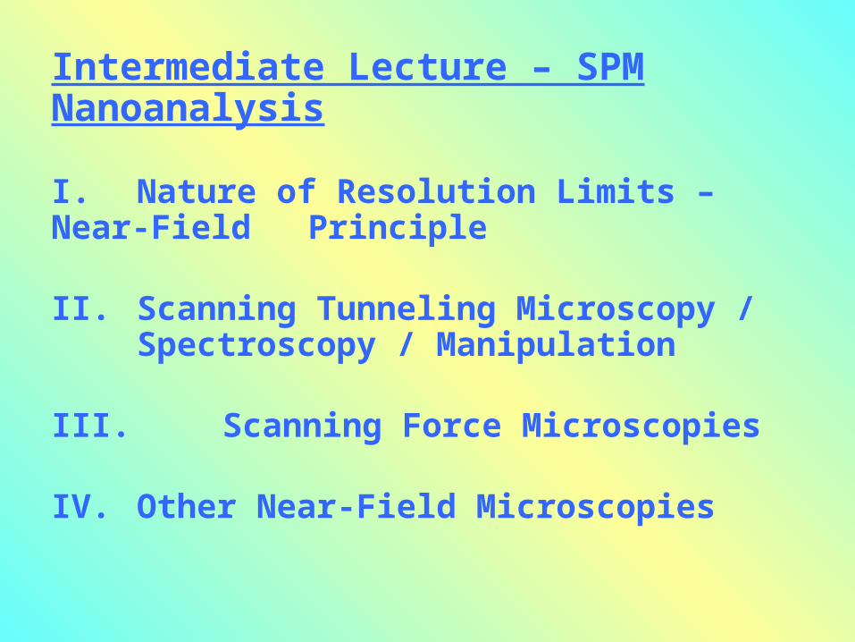
Intermediate Lecture – SPM Nanoanalysis
I. Nature of Resolution Limits – Near-Field Principle
II. Scanning Tunneling Microscopy / Spectroscopy / Manipulation
III. Scanning Force Microscopies
IV. Other Near-Field Microscopies
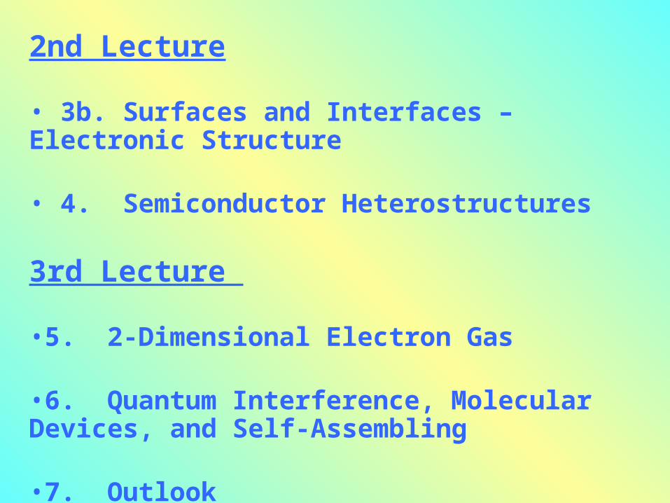
2nd Lecture
• 3b. Surfaces and Interfaces – Electronic Structure
• 4. Semiconductor Heterostructures
3rd Lecture
•5. 2-Dimensional Electron Gas
•6. Quantum Interference, Molecular Devices, and Self-Assembling
•7. Outlook
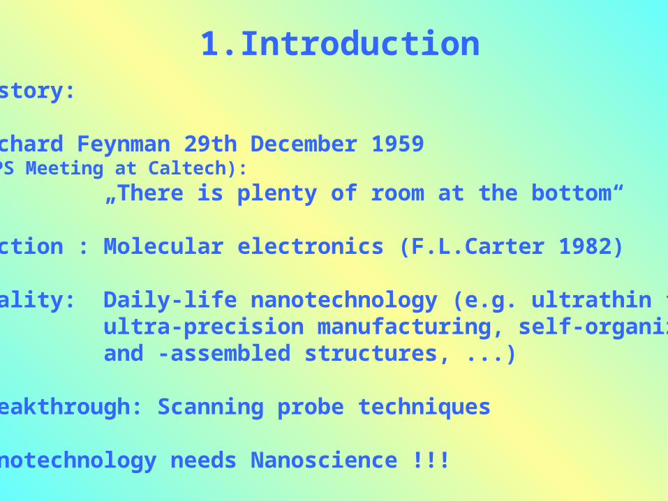
1.IntroductionHistory:
Richard Feynman 29th December 1959 (APS Meeting at Caltech):
„There is plenty of room at the bottom“
Fiction : Molecular electronics (F.L.Carter 1982)
Reality: Daily-life nanotechnology (e.g. ultrathin films,ultra-precision manufacturing, self-organizedand -assembled structures, ...)
Breakthrough: Scanning probe techniques
Nanotechnology needs Nanoscience !!!

Dimensional Considerations
1 nm = 10-9 m = 0.001 µm
Fe (bcc): d = 0.25 nm
A few nearest-neighbor distances in solids
1/1000 extension of a malaria bacterium
1 nm

A / V = 6a2 / a3 = 6 / a = 6 V-1/3
V = a3 (2a)3 = 8 a3 (5a)3 = 125 a3 (10a)3 = 1000 a3
Percentage of „surface atoms“:
100% 100% 78,4% 48,8%
Macroscopic: V = (108a)3 = 1024 a3 A = 6 (108a)2 = 6 1016 a2
Percentage of surface atoms: 6 10-8 % !!! (negligible)
Role of surface effects increases with decreasing dimensions
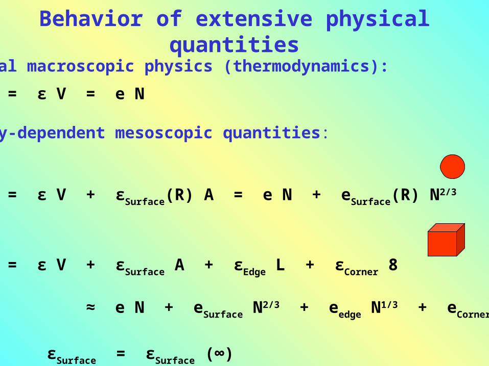
Behavior of extensive physical quantities
Classical macroscopic physics (thermodynamics):
E = ε V = e N
Geometry-dependent mesoscopic quantities:
Sphere:
E = ε V + εSurface(R) A = e N + eSurface(R) N2/3
Cube:
E = ε V + εSurface A + εEdge L + εCorner 8
≈ e N + eSurface N2/3 + eedge N
1/3 + eCorner N0
εSurface = εSurface (∞)

Application of Basic Physical Theories –
Classical vs. Quantum Physics:
mesoscopic phenomena (quasiclassical regime)
Classical MechanicsElectrodynamicsThermodynamics
Quantum MechnicsQuantum Electrodynamics
Quantum Statistics
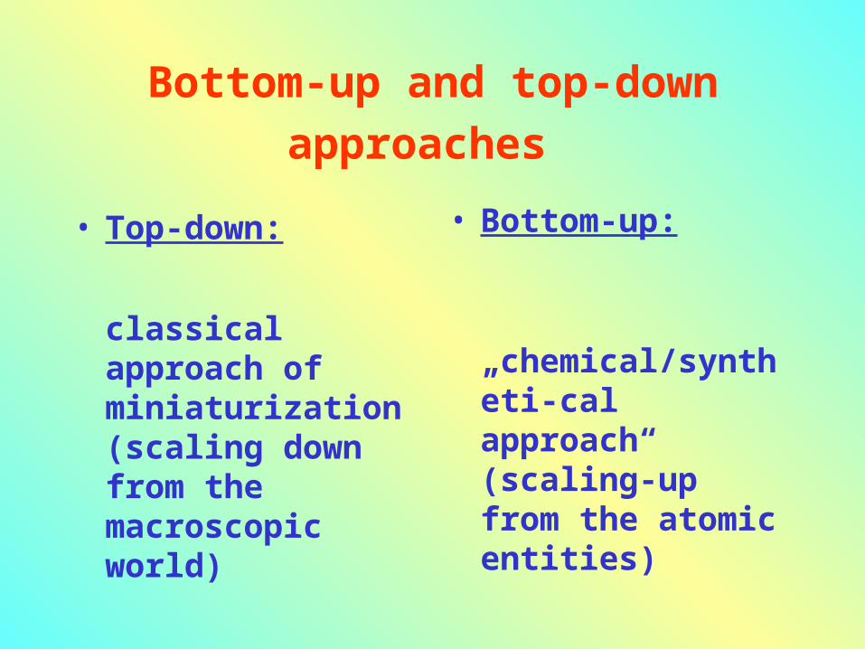
Bottom-up and top-down
approaches
• Top-down:
classical approach of miniaturization (scaling down from the macroscopic world)
• Bottom-up:
„chemical/syntheti-cal approach“ (scaling-up from the atomic entities)
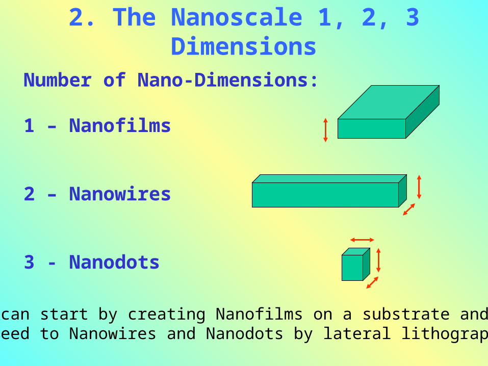
2. The Nanoscale 1, 2, 3 Dimensions
Number of Nano-Dimensions:
1 – Nanofilms
2 – Nanowires
3 - Nanodots
One can start by creating Nanofilms on a substrate and proceed to Nanowires and Nanodots by lateral lithography

Other Nanoobjects
Nanocomposites
Nanoporous Systems
High-velocity deformed nanostrucutred Nihttp://www.nanodynamics.com/ndMaterials.asp
Nanoporous luminescent Sihttp://www.chem.ucsb.edu/~buratto_group/PorousSilicon_1.htm

Supramolecular Architectures
J.-M.Lehnhttp://www.iupac.org/publications/pac/1994/pdf/6610x1961.pdf
C.J.Kuehlhttp://www.iupac.org/news/prize/2002/Kuehl-essay.pdf
3-dimensional functional structures according to the molecular geometri-cal and electronic structures
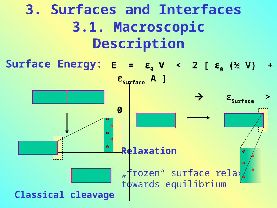
3. Surfaces and Interfaces 3.1. Macroscopic Description
Surface Energy:
Classical cleavage
Relaxation
„frozen“ surface relaxestowards equilibrium
E = ε0 V < 2 [ ε0 (½ V) + εSurface A ]
εSurface > 0
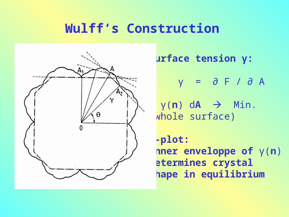
Wulff‘s Construction
Surface tension γ:
γ = ∂ F / ∂ A ∫ γ(n) dA Min.(whole surface)
γ-plot: inner enveloppe of γ(n) determines crystalshape in equilibrium
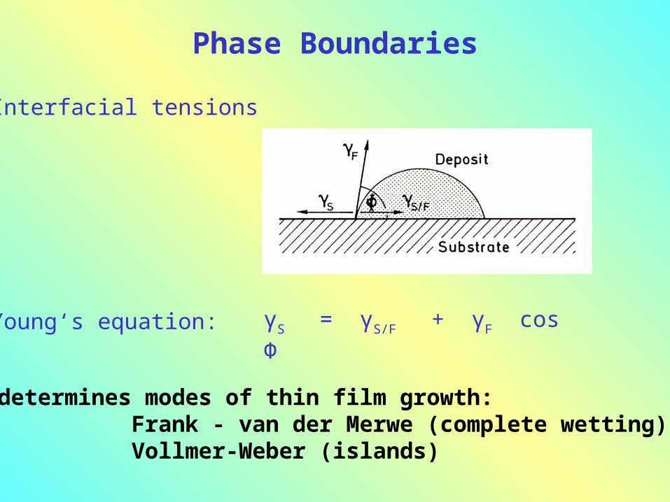
Phase Boundaries
Interfacial tensions
Young‘s equation: γS = γS/F + γF cos Ф
determines modes of thin film growth: Frank - van der Merwe (complete wetting) Vollmer-Weber (islands)
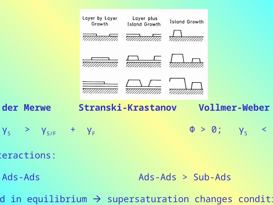
Frank-van der Merwe Stranski-Krastanov Vollmer-Weber
Ф = 0; γS > γS/F + γF Ф > 0; γS < γS/F + γF
Atomic interactions:
Sub-Ads > Ads-Ads Ads-Ads > Sub-Ads
only valid in equilibrium supersaturation changes conditions

3.2. Structure and Crystallography
of Surfaces
TLK model
(terraces, ledges,kinks)
Burton, Frank,Cabrera 1935
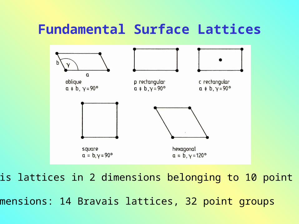
Fundamental Surface Lattices
5 Bravais lattices in 2 dimensions belonging to 10 point groups
in 3 dimensions: 14 Bravais lattices, 32 point groups

Miller Indices
Sections cutted from the axis
Take inverse of them
Multipy to get the smallest Integers
Axes parallel to surface – index 0
(1-10) (211)
x
y
z
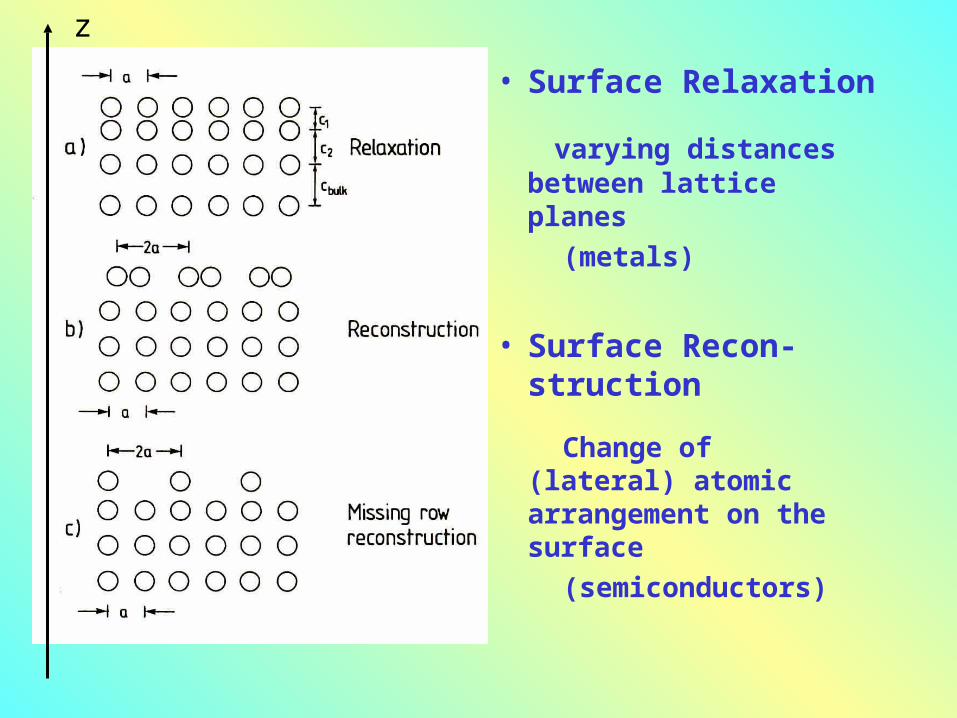
• Surface Relaxation
varying distances between lattice planes
(metals)
• Surface Recon-struction
Change of (lateral) atomic arrangement on the surface
(semiconductors)
z

Adsorbate Structuresz

Description of superstructures:
R = m a1 + n a2
Adsorbate / Rec. Surface Lattice: b1 = m11 a1 + m12 a2
b = M ab2 = m21 a1 + m22 a2
Area of new unit cell: |b1 x b2| = det M |a1 x a2|
integer simple
det M rational coincidence superlatticeirrational incommensurate
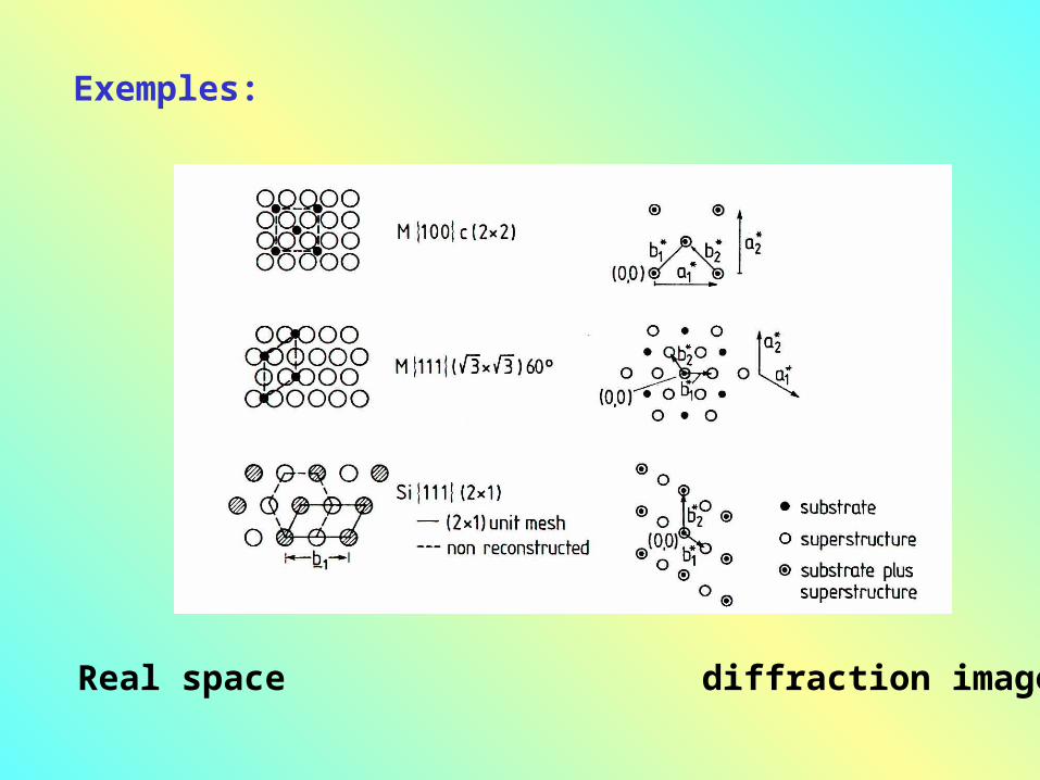
Exemples:
Real space diffraction image

Structure of interfaces
crystallinity and sharpnesscharacterize solid-solid interfaces
z
Related Documents