Nanophysics 15 Nanoelectronics (2) Tunnelling Supplementary materials

Welcome message from author
This document is posted to help you gain knowledge. Please leave a comment to let me know what you think about it! Share it to your friends and learn new things together.
Transcript

Nanophysics 15
Nanoelectronics (2) Tunnelling
Supplementary materials
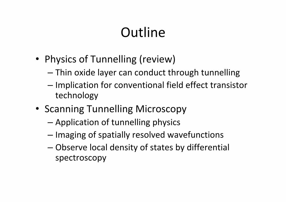
Outline
• Physics of Tunnelling (review)– Thin oxide layer can conduct through tunnelling
– Implication for conventional field effect transistor technology
• Scanning Tunnelling Microscopy– Application of tunnelling physics
– Imaging of spatially resolved wavefunctions
– Observe local density of states by differential spectroscopy
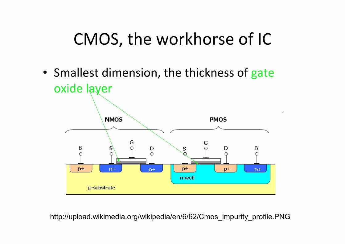
CMOS, the workhorse of IC
• Smallest dimension, the thickness of gate oxide layer
http://upload.wikimedia.org/wikipedia/en/6/62/Cmos_impurity_profile.PNG
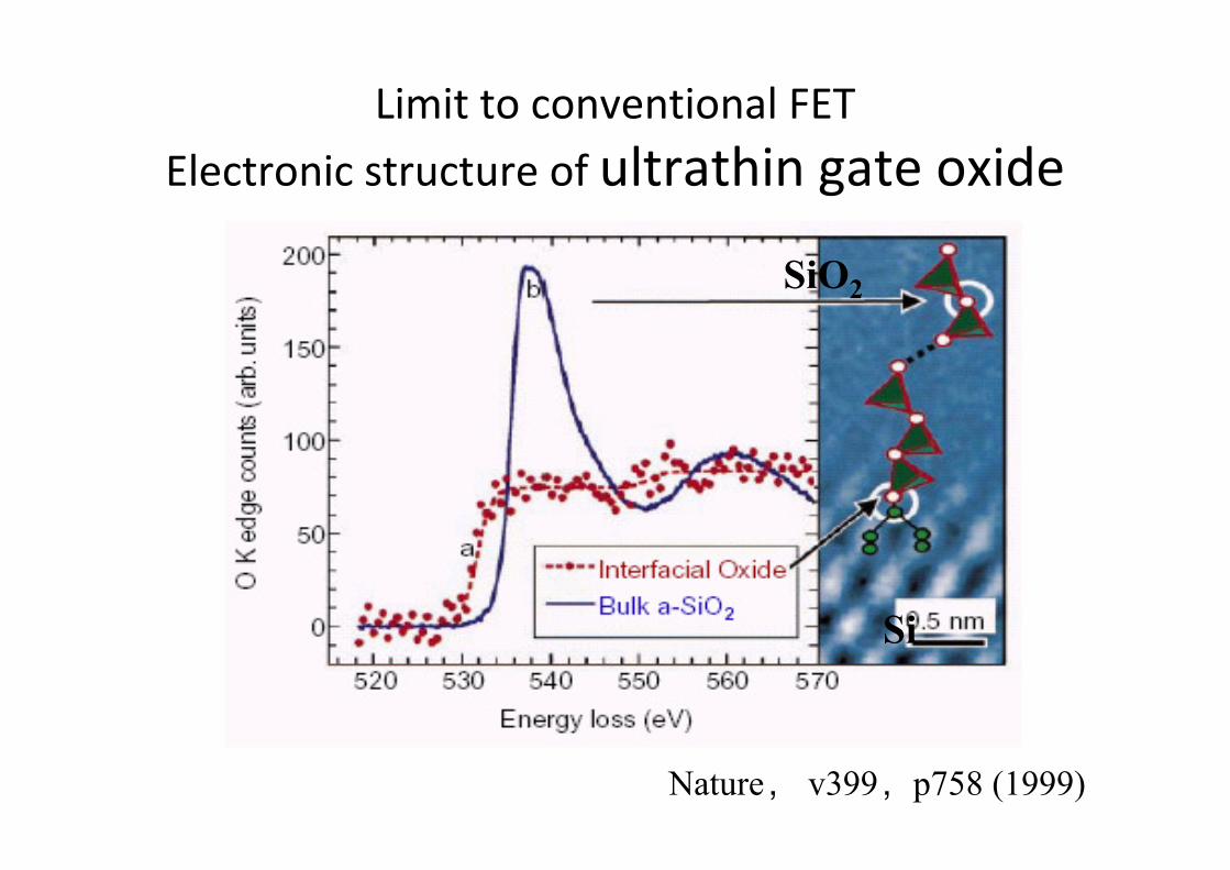
Limit to conventional FET
Electronic structure of ultrathin gate oxide
Nature, v399,p758 (1999)
SiO2
Si
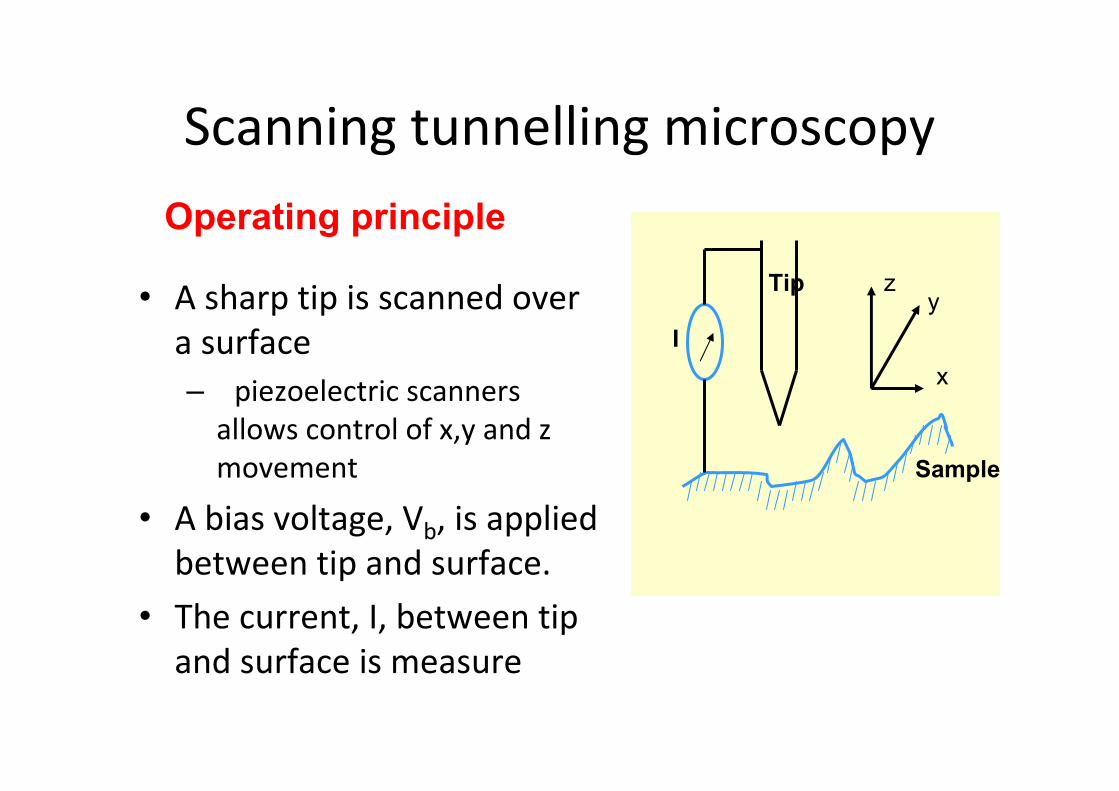
Tip
x
yz
Sample
I
Operating principle
Scanning tunnelling microscopy
• A sharp tip is scanned over a surface– piezoelectric scanners
allows control of x,y and z movement
• A bias voltage, Vb, is applied between tip and surface.
• The current, I, between tip and surface is measure
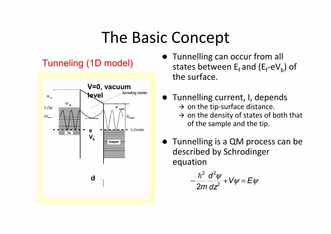
The Basic Concept� Tunnelling can occur from all
states between Ef and (Ef-eVb) of the surface.
� Tunnelling current, I, depends � on the tip-surface distance.� on the density of states of both that
of the sample and the tip.
� Tunnelling is a QM process can be described by Schrodinger equation
ψψψ
EVdz
d
m=+−
2
22
2
h
e
Vb
d
V=0, vacuum
level
Tunneling (1D model)
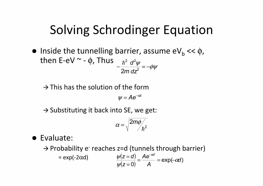
Solving Schrodinger Equation
� Inside the tunnelling barrier, assume eVb << φ, then E-eV ~ - φ, Thus
� This has the solution of the form
� Substituting it back into SE, we get:
� Evaluate:� Probability e- reaches z=d (tunnels through barrier)
= exp(-2αd)
φψψ
−=−2
22
2 dz
d
m
h
zAe αψ −=
22
h
φα m=
( )( )
)exp(0
dA
Ae
z
dz d
αψ
ψ α
−===
= −
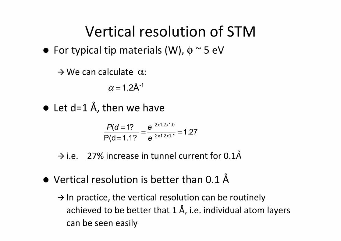
Vertical resolution of STM� For typical tip materials (W), φ ~ 5 eV
� We can calculate α:
� Let d=1 Å, then we have
� i.e. 27% increase in tunnel current for 0.1Å
� Vertical resolution is better than 0.1 Å
� In practice, the vertical resolution can be routinely
achieved to be better that 1 Å, i.e. individual atom layers
can be seen easily
1-Å2.1=α
27.11.1?P(d
?1(1.12.12
0.12.12
===
=−
−
xx
xx
e
edP
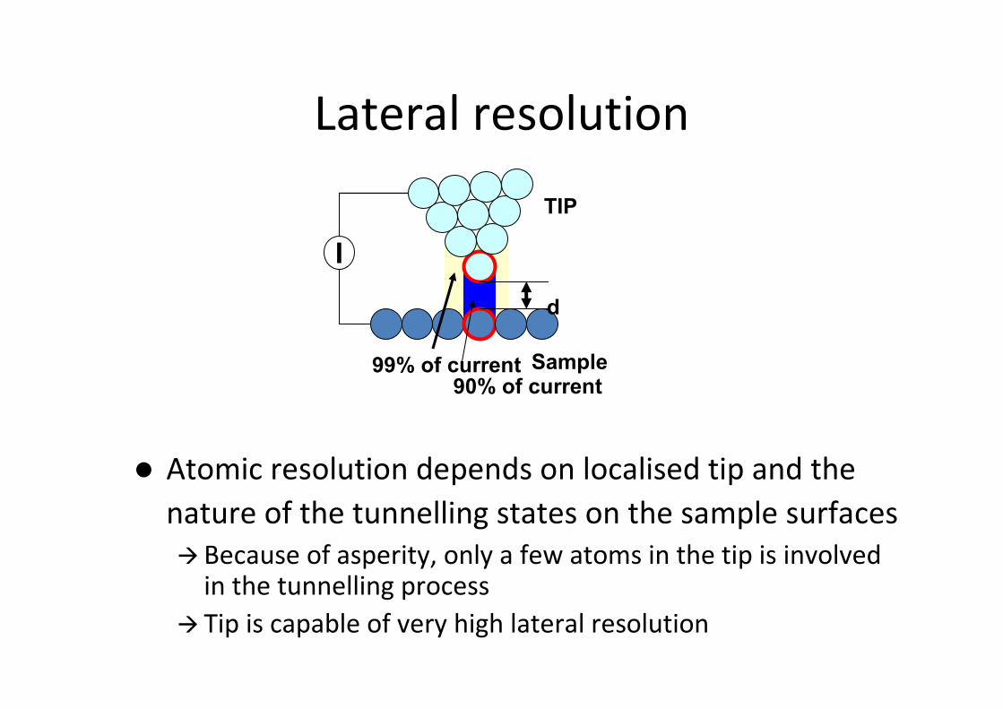
Lateral resolution
� Atomic resolution depends on localised tip and the
nature of the tunnelling states on the sample surfaces� Because of asperity, only a few atoms in the tip is involved
in the tunnelling process
� Tip is capable of very high lateral resolution
d
I
90% of current99% of current
TIP
Sample
Lateral resolution…
� Lateral atomic resolution depends on
� the wavefunction (whether localized or delocalized),
and
� the amount of charge spill over into interstitial space.
� Examples
� Cu(111)
� Si(100)
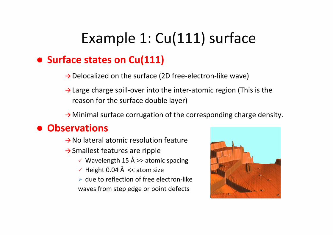
Example 1: Cu(111) surface� Surface states on Cu(111)
�Delocalized on the surface (2D free-electron-like wave)
�Large charge spill-over into the inter-atomic region (This is the
reason for the surface double layer)
�Minimal surface corrugation of the corresponding charge density.
� Observations�No lateral atomic resolution feature
�Smallest features are ripple � Wavelength 15 Å >> atomic spacing
� Height 0.04 Å << atom size
� due to reflection of free electron-like
waves from step edge or point defects
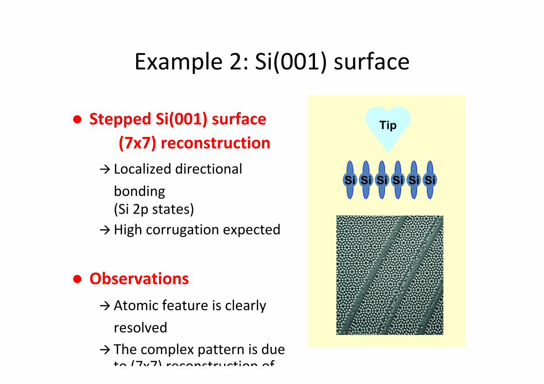
Example 2: Si(001) surface
� Stepped Si(001) surface
(7x7) reconstruction
� Localized directional
bonding (Si 2p states)
� High corrugation expected
� Observations
� Atomic feature is clearly
resolved
� The complex pattern is due to (7x7) reconstruction of
Si Si Si Si Si Si
Tip
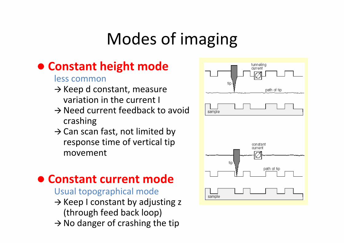
Modes of imaging
� Constant height modeless common� Keep d constant, measure
variation in the current I� Need current feedback to avoid
crashing� Can scan fast, not limited by
response time of vertical tip movement
� Constant current modeUsual topographical mode� Keep I constant by adjusting z
(through feed back loop)� No danger of crashing the tip
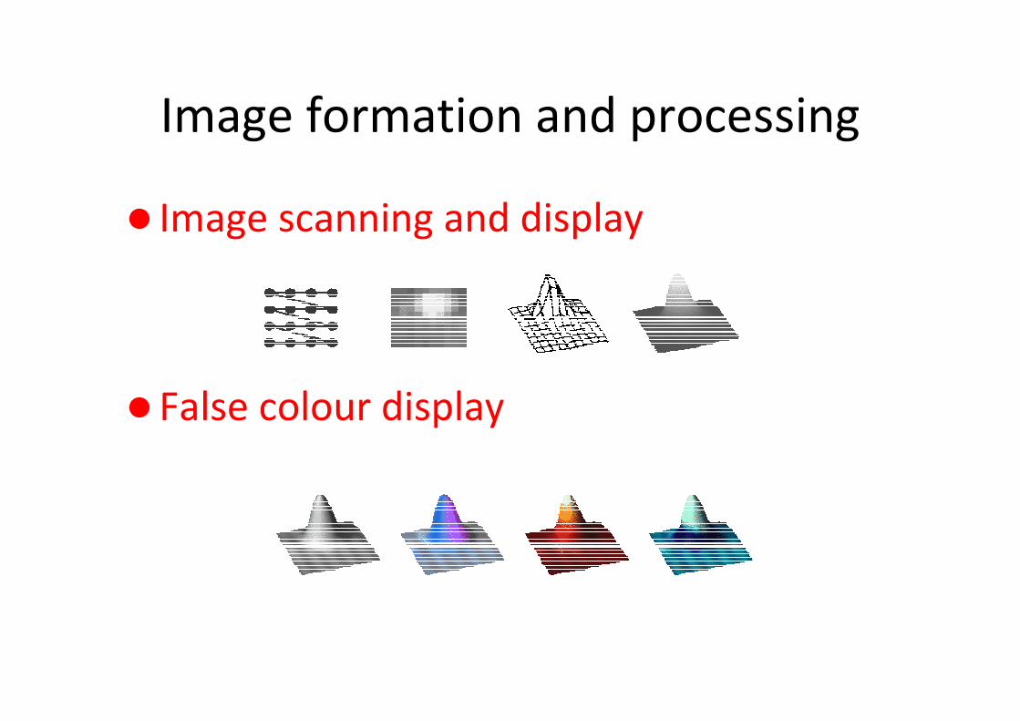
Image formation and processing
� Image scanning and display
� False colour display
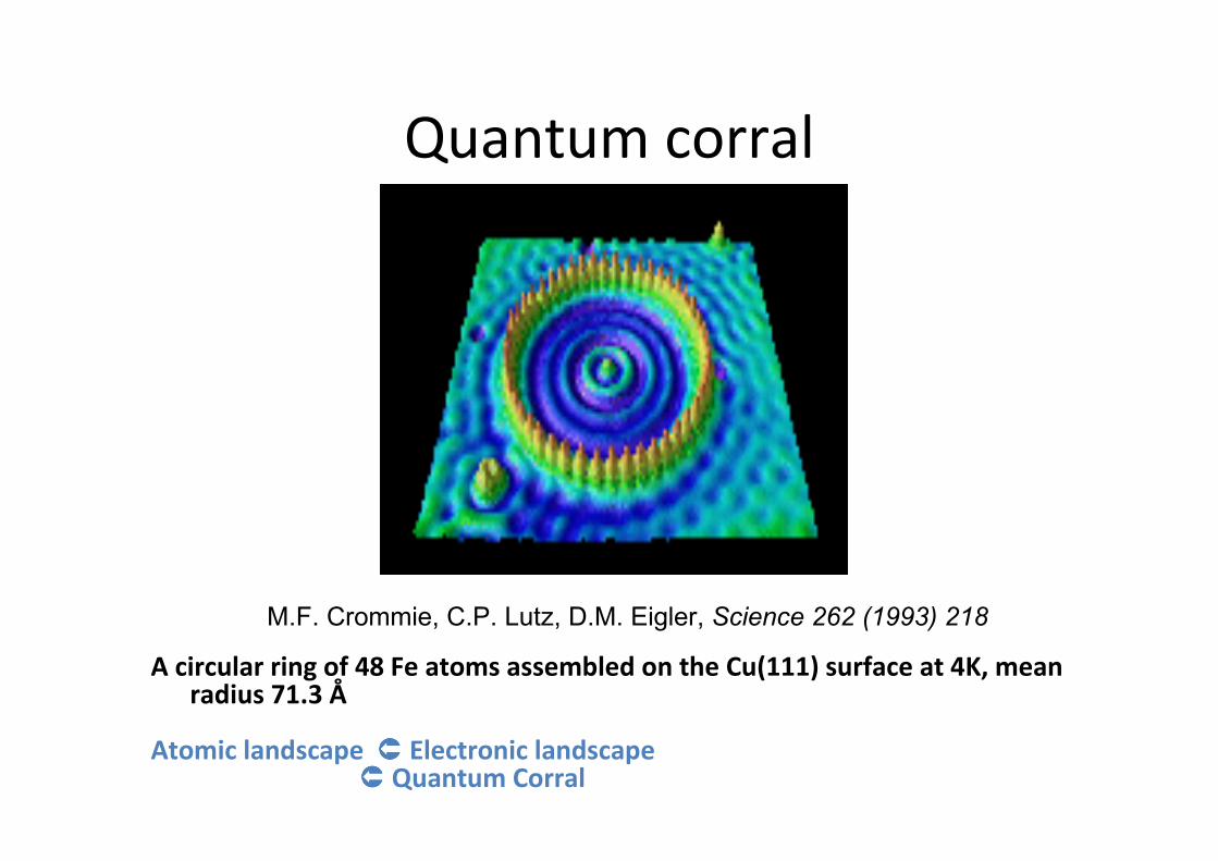
Quantum corral
A circular ring of 48 Fe atoms assembled on the Cu(111) surface at 4K, mean radius 71.3 Å
Atomic landscape ���� Electronic landscape ���� Quantum Corral
M.F. Crommie, C.P. Lutz, D.M. Eigler, Science 262 (1993) 218
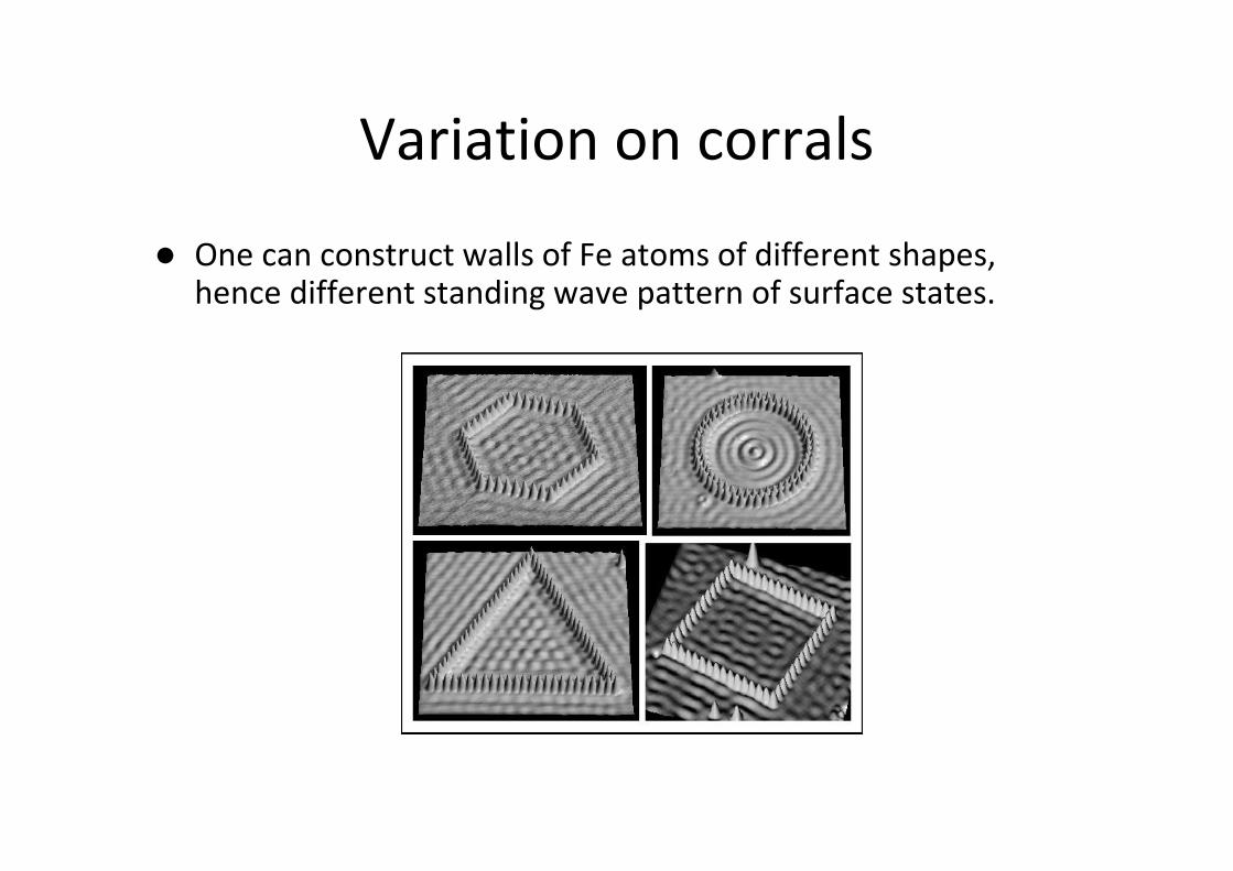
Variation on corrals
� One can construct walls of Fe atoms of different shapes, hence different standing wave pattern of surface states.
Quantum Corral
• The artificial corral structure results in space confinement of surface state wavefunction.
• The wave nature of the surface electron is demonstrated by the formation of ripples within the quantum corral.
• The ripple here and those found on stepped Cu(111) surface are of the same origin.
• In the case of quantum corral, the ripple pattern can be calculated using ‘particle in a box (ring)’ model
To understand the quantum quarrel• Understand the concept of surface states (revision)
– Free electron nature of surface states
• Understanding the interaction of impurity, steps with surface states– Reflection at steps and standing wave formation
• Experimental measurement of dispersion relationship (energy vs. wavevector) of the wavefunction
• Constructing quantum corrals to confine the wavefunction of the electrons in the surface state
• Understading of the electronic structure of the quantum corral– Solving two dimensional Schrodinger equation., solution for
wavefunction is based ob Bessel equations, energy level quantized. (explore the Bessel function, the zeros corresponds to the nodalpositions )
– STM image of the charge density (wavefunction squared)
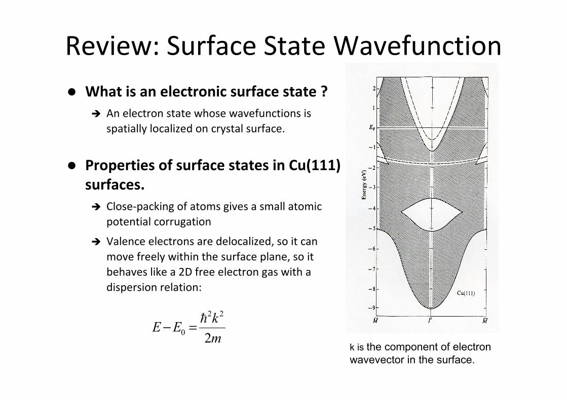
Review: Surface State Wavefunction
� What is an electronic surface state ?� An electron state whose wavefunctions is
spatially localized on crystal surface.
� Properties of surface states in Cu(111) surfaces.� Close-packing of atoms gives a small atomic
potential corrugation
� Valence electrons are delocalized, so it can move freely within the surface plane, so it behaves like a 2D free electron gas with a dispersion relation:
m
kEE
2
22
0
h=−
k is the component of electron wavevector in the surface.
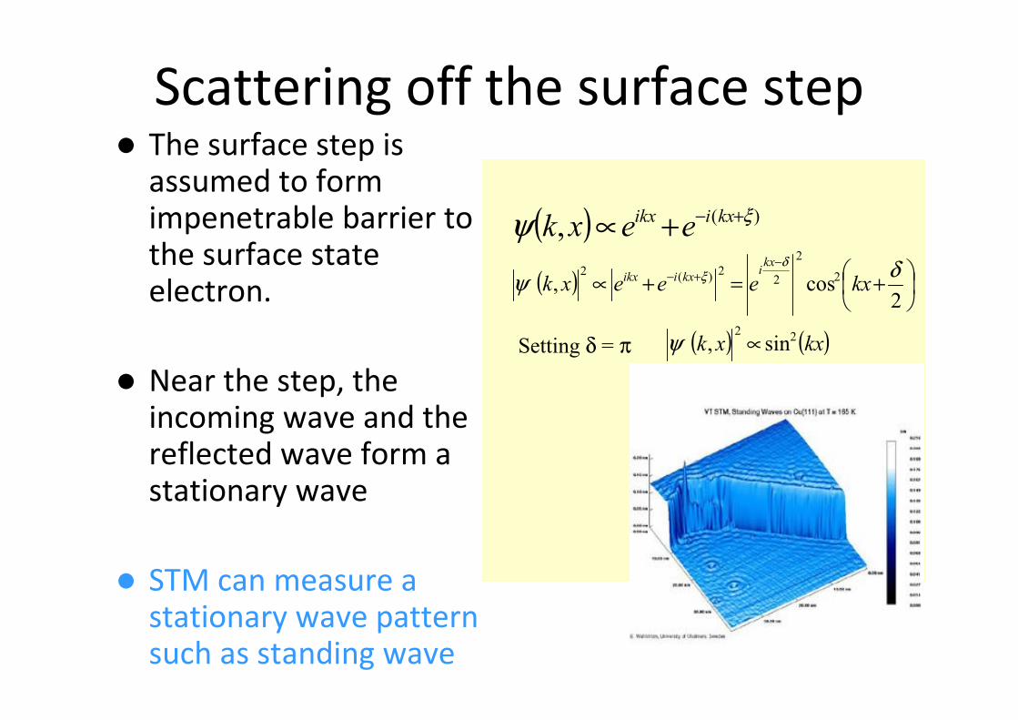
Scattering off the surface step� The surface step is
assumed to form impenetrable barrier to the surface state electron.
� Near the step, the incoming wave and the reflected wave form a stationary wave
� STM can measure a stationary wave pattern such as standing wave
( ) )(, ξψ +−+∝ kxiikx eexk
( )
+=+∝
−+−
2cos, 2
2
22)(
2 δψ
δξ kxeeexk
kxi
kxiikx
( ) ( )kxxk 22
sin, ∝ψSetting δ = π
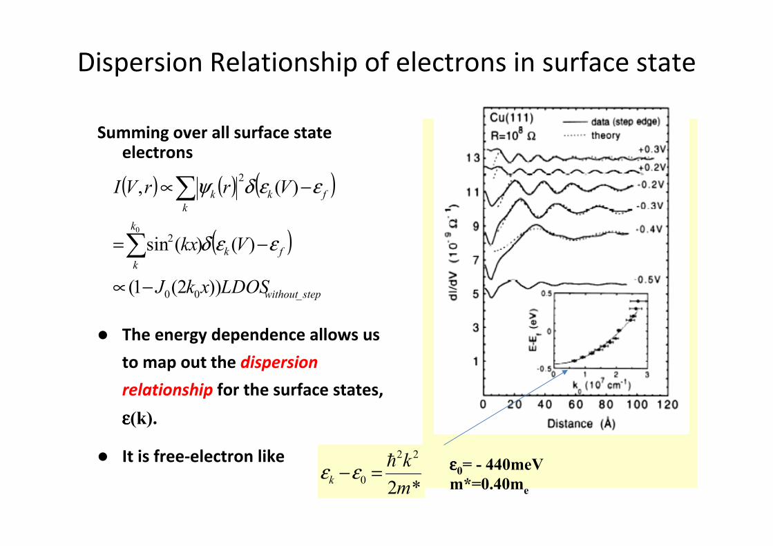
Dispersion Relationship of electrons in surface state
Summing over all surface state electrons
� The energy dependence allows us
to map out the dispersion
relationship for the surface states,
εεεε(k).
� It is free-electron like
( ) ( ) ( )
( )
stepwithout
fk
k
k
fk
k
k
LDOSxkJ
Vkx
VrrVI
_00
2
2
))2(1(
)()(sin
)(,
0
−∝
−=
−∝
∑
∑
εεδ
εεδψ
εεεε0= - 440meVm*=0.40me*2
22
0m
kk
h=−εε
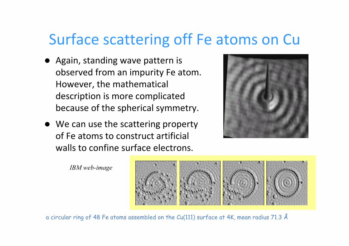
Surface scattering off Fe atoms on Cu� Again, standing wave pattern is
observed from an impurity Fe atom. However, the mathematical description is more complicated because of the spherical symmetry.
� We can use the scattering property of Fe atoms to construct artificial walls to confine surface electrons.
IBM web-image
a circular ring of 48 Fe atoms assembled on the Cu(111) surface at 4K, mean radius 71.3 Å
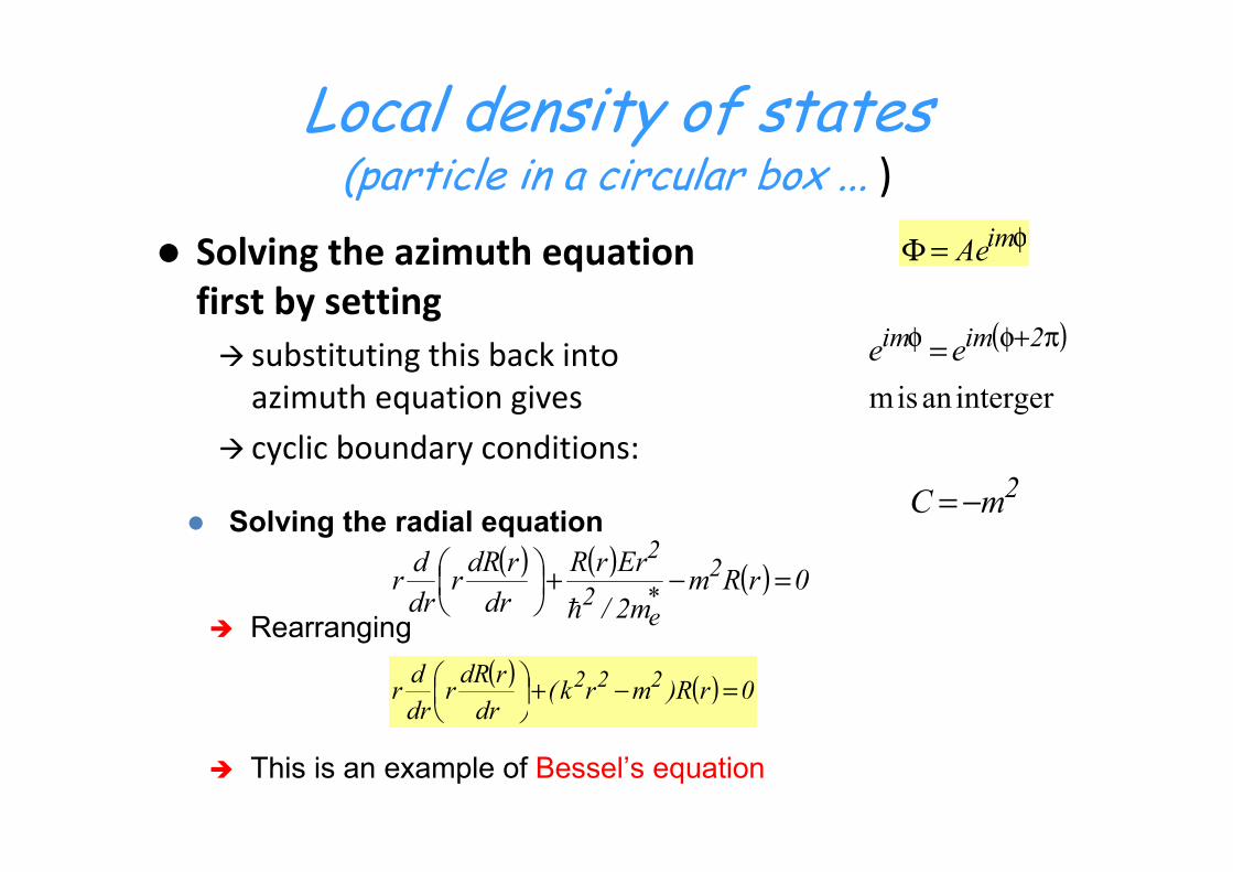
Local density of states(particle in a circular box ... )
� Solving the azimuth equation first by setting� substituting this back into
azimuth equation gives
� cyclic boundary conditions:
φ=Φ imAe
2mC −=
( )
intergeran is m
π+φφ = 2imim ee
( ) ( ) ( ) 0rRmm2/
ErrR
dr
rdRr
dr
dr 2
*e
2
2
=−+
h
( ) ( ) 0rR)mrk(dr
rdRr
dr
dr 222 =−+
� Solving the radial equation
� Rearranging
� This is an example of Bessel’s equation
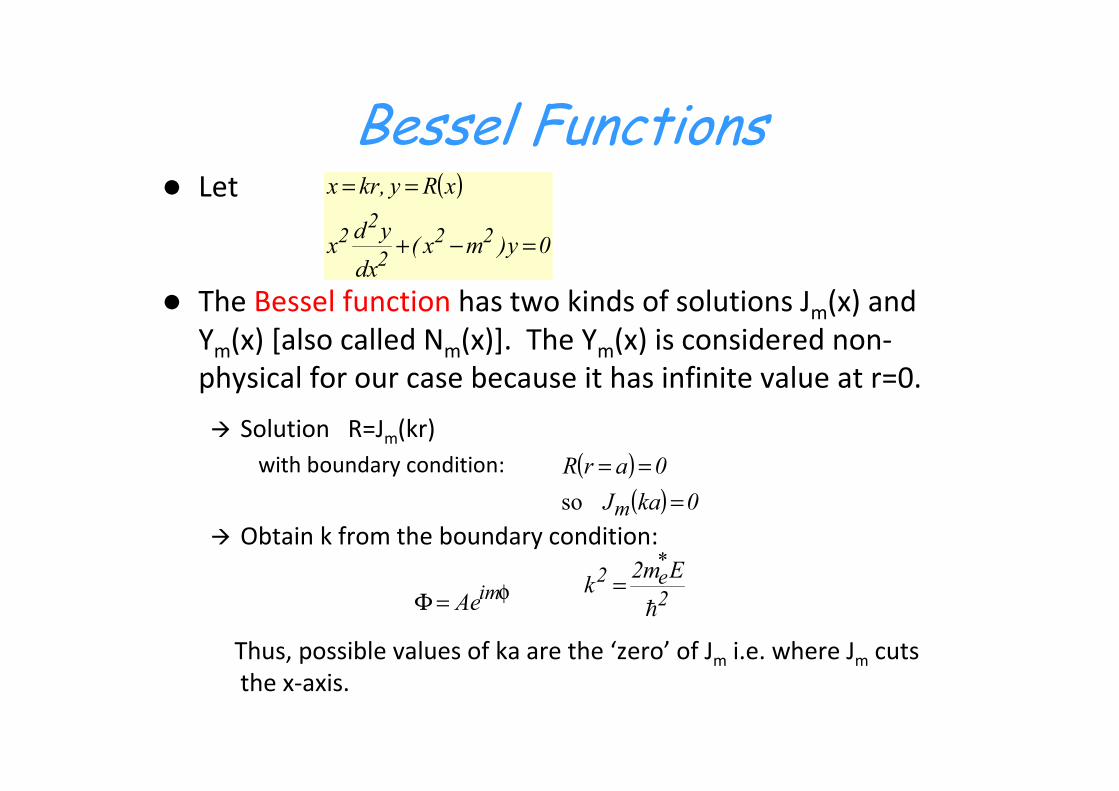
Bessel Functions� Let
� The Bessel function has two kinds of solutions Jm(x) and Ym(x) [also called Nm(x)]. The Ym(x) is considered non-physical for our case because it has infinite value at r=0.
� Solution R=Jm(kr)
with boundary condition:
� Obtain k from the boundary condition:
Thus, possible values of ka are the ‘zero’ of Jm i.e. where Jm cuts the x-axis.
( )( ) 0kaJ
0arR
m =
==
so
φ=Φ imAe 2
*e2 Em2
kh
=
( )
0y)mx(dx
ydx
xRy,krx
222
22 =−+
==
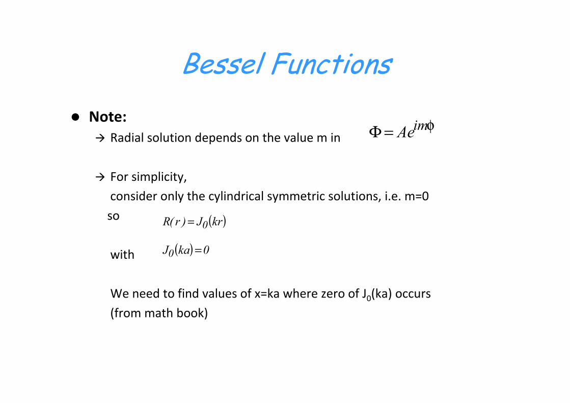
Bessel Functions
� Note:� Radial solution depends on the value m in
� For simplicity,
consider only the cylindrical symmetric solutions, i.e. m=0
so
with
We need to find values of x=ka where zero of J0(ka) occurs
(from math book)
( ) 0kaJ0 =
φ=Φ imAe
( )krJ)r(R 0=
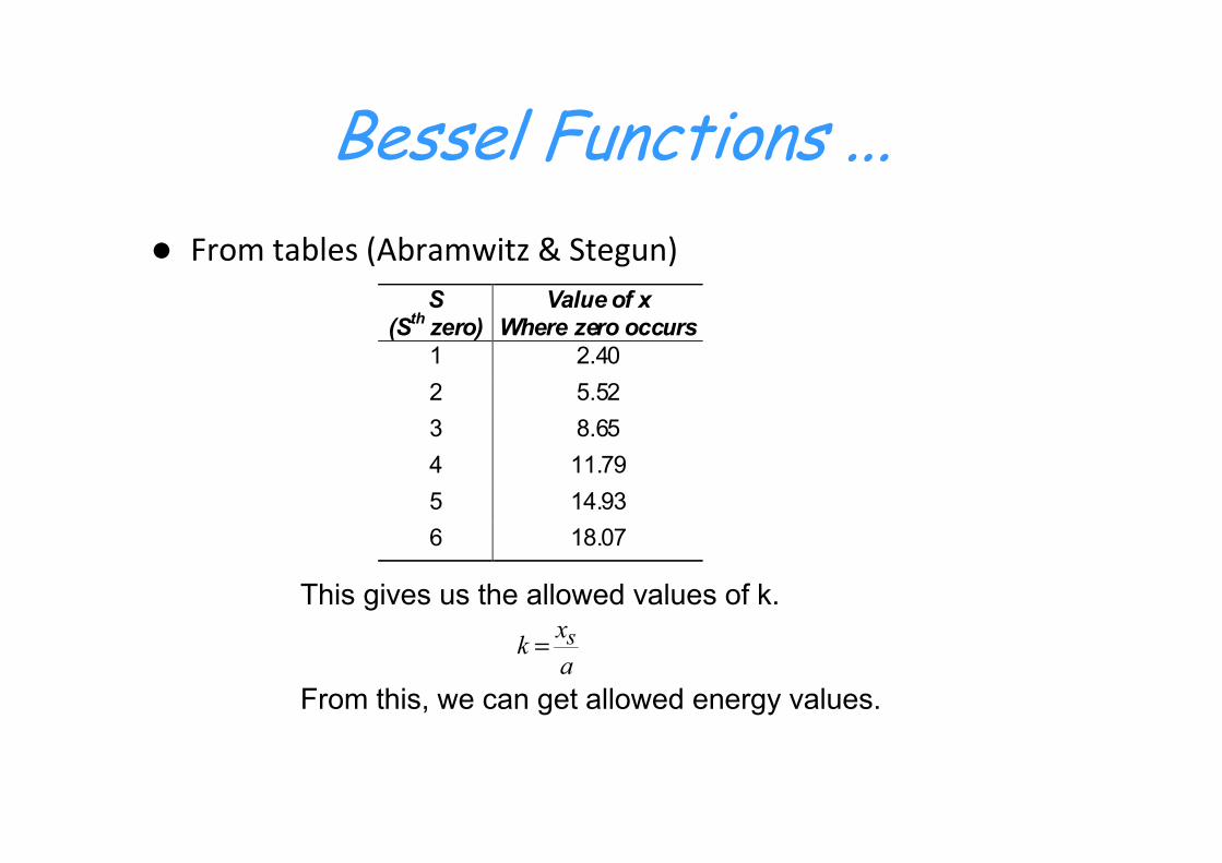
Bessel Functions ...� From tables (Abramwitz & Stegun)
This gives us the allowed values of k.
From this, we can get allowed energy values.a
xk s=
S(Sth zero)
Value of xWhere zero occurs
1 2.40
2 5.52
3 8.65
4 11.79
5 14.93
6 18.07
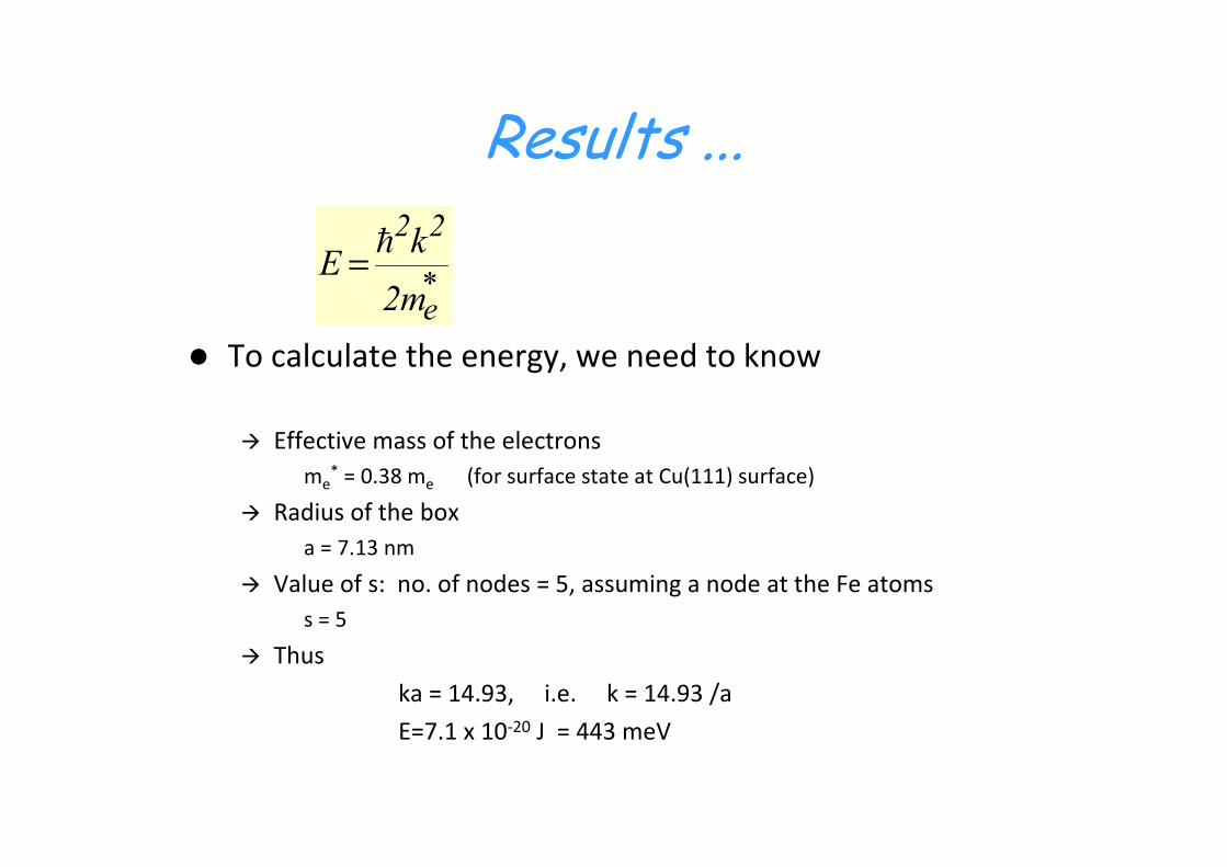
Results ...
� To calculate the energy, we need to know
� Effective mass of the electrons
me* = 0.38 me (for surface state at Cu(111) surface)
� Radius of the box
a = 7.13 nm
� Value of s: no. of nodes = 5, assuming a node at the Fe atoms
s = 5
� Thus
ka = 14.93, i.e. k = 14.93 /a
E=7.1 x 10⁻²⁰ J = 443 meV
*e
22
m2
kE
h=
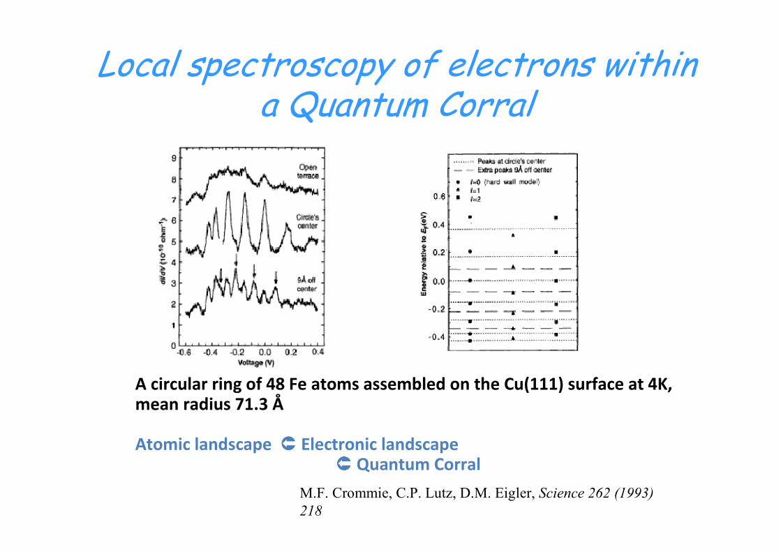
Local spectroscopy of electrons within a Quantum Corral
A circular ring of 48 Fe atoms assembled on the Cu(111) surface at 4K, mean radius 71.3 Å
Atomic landscape ���� Electronic landscape ���� Quantum Corral
M.F. Crommie, C.P. Lutz, D.M. Eigler, Science 262 (1993)
218
Comments ...� What is the reference point for V = 0 (bottom of the well) in the real
surface system ?
� Calculation: - 0.443eV
� Experiment: - 0.450 eV below FF
The s = 5 state lies at Ef,
The Vb used by Eigler was + 10 meV (on the sample)
� a remarkable match !!!
� If moving the tip out of the centre, pick up cylindrical unsymmetric, see additional peaks. Match well with m=1, 2, etc.
� The peak height (vs. r) do not quite match, so other waves are also present
� The peaks (vs. V) have a width (not δ function)� leakage out of the box or inelastic scattering
Summary
� Tunnelling is detrimental to FET� Tunnelling is very useful in STM� STM
� Applications to imaging of surface electronic state wavefunction�Surface state and its dispersion relationship.�The scattering property of atomic states and impurity Fe atoms on
Cu(111) �Confinement of surface electron states and standing wave pattern.
� Spectroscopy measurements using STM�STM current measures the sum of local density of states,
confirmation of the quantum mechanical calculation of a particle in a box
Related Documents


