Nanopatterning of Silicon Carbide by UV and Visible Lasers. By Arvind Battula 12/02/2004

Nanopatterning of Silicon Carbide by UV and Visible Lasers. By Arvind Battula 12/02/2004.
Dec 18, 2015
Welcome message from author
This document is posted to help you gain knowledge. Please leave a comment to let me know what you think about it! Share it to your friends and learn new things together.
Transcript

Nanopatterning of Silicon Carbide by UV and Visible Lasers.
By
Arvind Battula
12/02/2004

Properties of SiC.• Wide-gap semiconductor.
• High thermal conductivity.
• Low thermal expansion coefficient.
• High melting point.
• High hardness.
• High breakdown electric field.
• High electron saturation.
• Suitable for high temperature, power and frequency applications.

Photetching of SiC by VUV-266nm Multiwavelength.
Zhang, et. Al., 1996, “Direct photoetching of single crystal SiC by VUV-266 nm multiwavelength laser ablation”, Appl. Phys. A,64, p.367.

Femtosecond Pulsed Laser Induced 3C/SiC surface Morphology.
Pulse duration = 120 fs; wavelength = 800 nm
Dong.Y., and Molian. P., 2003, “Femtosecond pulsed laser ablation of 3C-SiC thin film on Silicon”, Appl. Phys. A, 77, p. 839

Monolayer of SiO2 Nano-spheres on SiC.
SEM micrograph of the monolayer of silica spheres diameters (a) 1.76 µm and (b) 640 nm.

Experimental Setup.
LaserHarmonic Separator
Lens
XY Stage
Aperture
SiC Substrate
Silica Nanospheres
Laser
Schematic of (a) experimental setup, (b) Irradiation of the spheres on SiC.
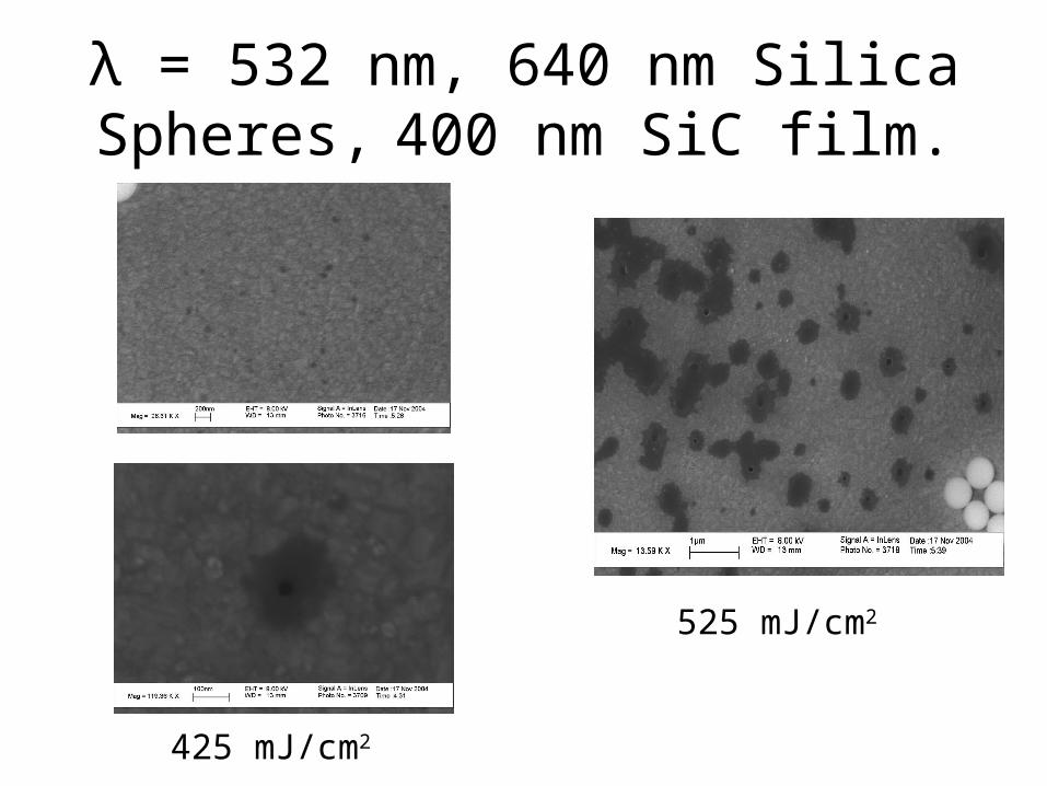
λ = 532 nm, 640 nm Silica Spheres,
400 nm SiC film.
425 mJ/cm2
525 mJ/cm2

λ = 532 nm, 1.76 µm Silica Spheres, 400 nm SiC film.
275 mJ/cm2
400 mJ/cm2
200 mJ/cm2
325 mJ/cm2

λ = 355 nm, 640 nm Silica Spheres, 400 nm SiC film.
400 mJ/cm2
500 mJ/cm2
300 mJ/cm2

λ = 355 nm, 1.76 µm Silica Spheres, 400 nm SiC film
350 mJ/cm2225 mJ/cm2
225 mJ/cm2175 mJ/cm2

Gradual Changes in the Melting Zone of one Laser Spot.

λ = 532 nm, 250 nm Gold Spheres, 300 mJ/cm2 , 200 nm SiC film.

λ = 355 nm, 250 nm Gold Spheres, 425 mJ/cm2 , 200 nm SiC film.

Features for 355 nm Laser on Bulk SiC.
Features formed on the SiC substrate with a 355 nm laser (a) 1.76 µm diameter spheres and 950 mJ/cm2 and (b) 640 nm diameter spheres and 850 mJ/cm2.

AFM Results for 355 nm Laser.
Variation in the feature size with respect to the laser intensity for 355 nm laser and 1.76 µm spheres.

Features for 532 nm Laser on Bulk SiC.
750 nm1 µm
Features formed on the SiC substrate with a 532 nm laser (a) 1.76 µm diameter spheres and 2 J/cm2 and (b) 640 nm diameter spheres and 6 J/cm2.

AFM Results for 532 nm Laser.
AFM cross section view of the features obtained with 532 nm laser and 1.76 µm spheres.

Ablation Mechanism.• At low laser fluence the formation of laser-induced nanostructures
are from defect-activation.
• The pre-existing defects facilitate local absorption of incident laser.
• This results crystalline SiC to lattice disorder due to electronic excitation.
• Weakens interatomic bonding and thus lower the vibrational energy required for lattice disorder.
• With increasing laser-induced lattice defects, the formation of grain boundries results in polycrystallization of SiC film.

Non-Thermal Transitions in Semiconductors.
S.K. Sundaram and E. Mazur, “Inducing and Probing Non-Thermal Transitions in Semiconductors Using Femtosecond Laser Pulses”, Nature Materials, 1, 217-224 (2002).
Related Documents