University of Tennessee, Knoxville University of Tennessee, Knoxville TRACE: Tennessee Research and Creative TRACE: Tennessee Research and Creative Exchange Exchange Doctoral Dissertations Graduate School 12-2018 Multi-Frequency Modulation and Control for DC/AC and AC/DC Multi-Frequency Modulation and Control for DC/AC and AC/DC Resonant Converters Resonant Converters Chongwen Zhao University of Tennessee, [email protected] Follow this and additional works at: https://trace.tennessee.edu/utk_graddiss Recommended Citation Recommended Citation Zhao, Chongwen, "Multi-Frequency Modulation and Control for DC/AC and AC/DC Resonant Converters. " PhD diss., University of Tennessee, 2018. https://trace.tennessee.edu/utk_graddiss/5269 This Dissertation is brought to you for free and open access by the Graduate School at TRACE: Tennessee Research and Creative Exchange. It has been accepted for inclusion in Doctoral Dissertations by an authorized administrator of TRACE: Tennessee Research and Creative Exchange. For more information, please contact [email protected].

Welcome message from author
This document is posted to help you gain knowledge. Please leave a comment to let me know what you think about it! Share it to your friends and learn new things together.
Transcript
University of Tennessee, Knoxville University of Tennessee, Knoxville
TRACE: Tennessee Research and Creative TRACE: Tennessee Research and Creative
Exchange Exchange
Doctoral Dissertations Graduate School
12-2018
Multi-Frequency Modulation and Control for DC/AC and AC/DC Multi-Frequency Modulation and Control for DC/AC and AC/DC
Resonant Converters Resonant Converters
Chongwen Zhao University of Tennessee, [email protected]
Follow this and additional works at: https://trace.tennessee.edu/utk_graddiss
Recommended Citation Recommended Citation Zhao, Chongwen, "Multi-Frequency Modulation and Control for DC/AC and AC/DC Resonant Converters. " PhD diss., University of Tennessee, 2018. https://trace.tennessee.edu/utk_graddiss/5269
This Dissertation is brought to you for free and open access by the Graduate School at TRACE: Tennessee Research and Creative Exchange. It has been accepted for inclusion in Doctoral Dissertations by an authorized administrator of TRACE: Tennessee Research and Creative Exchange. For more information, please contact [email protected].

To the Graduate Council:
I am submitting herewith a dissertation written by Chongwen Zhao entitled "Multi-Frequency
Modulation and Control for DC/AC and AC/DC Resonant Converters." I have examined the final
electronic copy of this dissertation for form and content and recommend that it be accepted in
partial fulfillment of the requirements for the degree of Doctor of Philosophy, with a major in
Electrical Engineering.
Daniel Costinett, Major Professor
We have read this dissertation and recommend its acceptance:
Fred Wang, Leon M. Tolbert, D. Caleb Rucker
Accepted for the Council:
Dixie L. Thompson
Vice Provost and Dean of the Graduate School
(Original signatures are on file with official student records.)

Multi-Frequency Modulation and Control for
DC/AC and AC/DC Resonant Converters
A Dissertation Presented for the
Doctor of Philosophy
Degree
University of Tennessee, Knoxville
Chongwen Zhao
December 2018

ii
To my parents
To Junting Guo

iii
Acknowledgement
I would like to acknowledge the support and guidance from faculty members and staff at the
University of Tennessee. My advisor, Dr. Daniel Costinett, always shares his passion and
enthusiasm with me, on the path of pursuing my Ph.D. degree. This motivates me to accomplish
my degree and refine myself as a human being. Dr. Leon Tolbert is a great mentor and talking to
him is always my honor and pleasure. Dr. Fred Wang is an example of excellence and asking
questions in his class gives me plenty of intellectual joy. Dr. Chien-fei Chen, Dr. Nicole McFarlane,
Dr. Caleb Rucker, Dr. Donatello Materassi, Dr. Benjamin Blalock and Mr. Robert Martin give me
many good advices during my study, and I would like to express my appreciation to them.
I build beautiful friendships with my colleagues who came to UTK the same year, though some
of them are out of town and having their marvelous adventures. Special appreciations to Dr. Bo
Liu, Dr. Wenyun Ju and Mr. Ren Ren for numerous days working and hanging out together. The
senior colleagues in the lab own sympathy and are helpful, a great trait of the CURENT center.
The young generations are vigorous and working hard, paving a bright future. So glad that I have
a great time here.
The Doctor of Philosophy stems from the golden Greek time, and an experience expanding the
knowledge boundary links me to those BIG names. No matter the world is physical or spiritual,
may the knowledge long live.
iv
Abstract
Harmonic content is inherent in switched-mode power supplies. Since the undesired harmonics
interfere with the operation of other sensitive electronics, the reduction of harmonic content is
essential for power electronics design. Conventional approaches to attenuate the harmonic content
include passive/active filter and wave-shaping in modulation. However, those approaches are not
suitable for resonant converters due to bulky passive volumes and excessive switching losses. This
dissertation focuses on eliminating the undesired harmonics from generation by intelligently
manipulating the spectrum of switching waveforms, considering practical needs for functionality.
To generate multiple ac outputs while eliminating the low-order harmonics from a single
inverter, a multi-frequency programmed pulse width modulation is investigated. The proposed
modulation schemes enable multi-frequency generation and independent output regulation. In this
method, the fundamental and certain harmonics are independently controlled for each of the
outputs, allowing individual power regulations. Also, undesired harmonics in between output
frequencies are easily eliminated from generation, which prevents potential hazards caused by the
harmonic content and bulky filters. Finally, the proposed modulation schemes are applicable to a
variety of DC/AC topologies.
Two applications of dc/ac resonant inverters, i.e. an electrosurgical generator and a dual-mode
WPT transmitter, are demonstrated using the proposed MFPWM schemes. From the experimental
results of two hardware prototypes, the MFPWM alleviates the challenges of designing a
complicated passive filter for the low-order harmonics. In addition, the MFPWM facilitates
combines functionalities using less hardware compared to the state-of-the-art. The prototypes
demonstrate a comparable efficiency while achieving multiple ac outputs using a single inverter.

v
To overcome the low-efficiency, low power-density problems in conventional wireless fast
charging, a multi-level switched-capacitor ac/dc rectifier is investigated. This new WPT receiver
takes advantage of a high power-density switched-capacitor circuit, the low harmonic content of
the multilevel MFPWMs, and output regulation ability to improve the system efficiency. A
detailed topology evaluation regarding the regulation scheme, system efficiency, current THD and
volume estimation is demonstrated, and experimental results from a 20 W prototype prove that the
multi-level switched-capacitor rectifier is an excellent candidate for high-efficiency, high power
density design of wireless fast charging receiver.

vi
Table of Contents
1. Introduction ................................................................................................................................1
1.1 Applications of Resonant Converters ............................................................................. 4
1.1.1 Electrosurgical Power Supply .................................................................................. 5
1.1.2 Wireless Power Transfer System ............................................................................. 7
1.2 Summary ....................................................................................................................... 10
2. Harmonic Content in Resonant Converter ............................................................................12
2.1 Contributing Factors of Harmonic Content .................................................................. 13
2.2 Modulation Schemes for SMPS .................................................................................... 15
2.1.1 Carrier-based Pulse Width Modulation ................................................................. 15
2.2.2 Space Vector Modulation ...................................................................................... 16
2.2.3 Programmed Pulse Width Modulation................................................................... 18
2.3 Modulation and Control of Resonant Converter ........................................................... 19
2.4 Dissertation Organization ............................................................................................. 20
3. Literature Review ....................................................................................................................23
3.1 Harmonic Content Reduction Approach ....................................................................... 23
3.1.1 Hardware-based Approaches ................................................................................. 24
3.1.2 Software-based Approach ...................................................................................... 25
3.2 Programmed PWM ....................................................................................................... 26
3.2.1 Programmed PWM Problem Formation ................................................................ 26
3.2.2 Solving Algorithm ................................................................................................. 28
3.3 Multi-frequency Generation Approaches ..................................................................... 31
3.3.1 Separate-Converter Configuration ......................................................................... 31
3.3.2 Single-Converter Configuration ............................................................................. 35
3.4 Challenge and Motivation ............................................................................................. 37

vii
4. Multi-Frequency Programmed Pulse Width Modulation ....................................................38
4.1 Benchmark Evaluation .................................................................................................. 39
4.1.1 Duty Cycle Modulation.......................................................................................... 40
4.1.2 Carrier-based PWM ............................................................................................... 42
4.1.3 SHE ........................................................................................................................ 44
4.1.4 Summary ................................................................................................................ 48
4.2 MFPWM Formulation: Unipolar, Bipolar and Phase-shift ........................................... 49
4.2.1 Unipolar MFPWM ................................................................................................. 49
4.1.2 Bipolar MFPWM ................................................................................................... 52
4.1.3 Phase-shift MFPWM ............................................................................................. 54
4.3 MFPWM Evaluation ..................................................................................................... 60
4.3.1 Modulation range ................................................................................................... 60
4.3.2 Switching loss ........................................................................................................ 68
4.3.3 Harmonic content ................................................................................................... 68
4.3.4 Summary ................................................................................................................ 70
4.4 MFPWM Extension ...................................................................................................... 70
4.4.1 MFPWM with Extended Switching Angles .......................................................... 71
4.4.2 MFPWM with Flexible Output Combination ........................................................ 75
4.4.3 Multilevel MFPWM............................................................................................... 79
4.4.4 Full Solution of MFPWM ...................................................................................... 81
4.5 Conclusion .................................................................................................................... 84
5. MFPWM for Resonant DC/AC Inverter Applications .........................................................85
5.1 Multi-Mode Electrosurgical Generator ......................................................................... 85
5.1.1 Implementation of Multi-mode ESG ..................................................................... 86
5.1.2 Experimental results............................................................................................... 90

viii
5.2 Dual-Mode WPT Transmitter ....................................................................................... 94
5.2.1 Wideband Dual-mode WPT ................................................................................... 95
5.2.2 Narrowband Dual-mode WPT ............................................................................... 99
5.2.3 Experimental Results ........................................................................................... 102
5.2.4 Discussion ............................................................................................................ 111
5.3 Conclusion .................................................................................................................. 114
6. Evaluation of AC/DC Rectifier for Wireless Fast Charging ..............................................116
6.1 WPT Receiver: Candidate Topology Review ............................................................. 117
6.1.1 Diode Rectifier ..................................................................................................... 118
6.1.2 Diode Rectifier plus 3:1 step-down Buck Converter ........................................... 122
6.1.3 Synchronous Rectifier Plus Switched-Capacitor DC/DC Converter ................... 126
6.1.4 Seven-level Switched Capacitor 3:1 Step-down AC-DC Rectifier ..................... 128
6.1.5 Summary .............................................................................................................. 133
6.2 Function Simulation and Loss Estimation .................................................................. 136
6.2.1 Diode Rectifier ..................................................................................................... 136
6.2.2 Diode Rectifier plus 3:1 step-down Buck Converter ........................................... 141
6.2.3 Synchronous Rectifier Plus Switched-Capacitor DC/DC Converter ................... 145
6.2.4 Seven-level Switched Capacitor 3:1 step-down AC-DC Rectifier ...................... 151
6.2.5 Charge Control for MSC Rectifier ....................................................................... 156
6.2.6 Summary .............................................................................................................. 164
6.3 THD Analysis ............................................................................................................. 165
6.3.1 Current THD modeling ........................................................................................ 165
6.3.2 THD minimization approach ............................................................................... 173
6.3.3 Summary .............................................................................................................. 179
6.4 Volume Estimation ..................................................................................................... 181

ix
6.5 Conclusion .................................................................................................................. 183
7. Design and Implementation of MSC Rectifier ....................................................................186
7.1 Device Sizing for Integrated Circuit Design ............................................................... 186
7.1.1 5 level SC Rectifier .............................................................................................. 187
7.1.2 Synchronous Rectifier plus 2:1 SC converter ...................................................... 192
7.1.3 Reduction of Charge Sharing Loss ...................................................................... 197
7.1.4 Summary .............................................................................................................. 199
7.2 Regulation Design using MSC rectifier ...................................................................... 201
7.2.1 Output Regulation using MSC rectifier ............................................................... 201
7.2.2 Closed-loop Design for MSC rectifier ................................................................. 205
7.3 Experimental Results .................................................................................................. 211
7.3.1 Efficiency test ...................................................................................................... 213
7.3.2 THD test ............................................................................................................... 219
7.3.3 Closed-loop control test ....................................................................................... 226
8. Conclusion and Future Work ...............................................................................................230
8.1 Conclusion .................................................................................................................. 230
8.2 Future work ................................................................................................................. 233
List of Reference ........................................................................................................................235
Appendix .....................................................................................................................................244
A.1 WBG Device Selection .............................................................................................. 245
A.2 GaN Device Loss Modeling ....................................................................................... 247
A.3 Driver Circuit Design and Thermal Implementation ................................................. 250
Vita ..............................................................................................................................................256

x
List of Tables
TABLE. 4-1. METRIC COMPARISON OF THREE MODULATION ...................................................... 48
TABLE. 4-2. MODULATION RANGE COMPARISON OF MFPWM (SA = 3) .................................... 61
TABLE. 4-3. METRIC COMPARISON OF THREE MFPWM ............................................................ 71
TABLE. 4-4. INITIAL VALUES TO SOLVE BIPOLAR MFPWM W/ 35 SWITCHING-ANGLE (UNIT:
DEGREE) ........................................................................................................................................ 72
TABLE. 4-5. INITIAL VALUES TO SOLVE UNIPOLAR MFPWM W/ 35 SWITCHING-ANGLE (UNIT:
DEGREE) ........................................................................................................................................ 72
TABLE. 5-1. SPECIFICATION OF MULTI-MODE ESG PROTOTYPE ................................................. 91
TABLE. 5-2. CALCULATED MFPWM THDS (5SA & 7SA) ......................................................... 94
TABLE. 5-3. SYSTEM SPECIFICATIONS OF PROPOSED DUAL-MODE WPT TRANSMITTER .......... 104
TABLE. 5-4. MFPWM ACCURACY COMPARISON OF PRE-DETERMINED VALUES AND EXPERIMENTAL
RESULTS ....................................................................................................................................... 111
TABLE. 5-5. PERFORMANCE COMPARISON WITH STATE-OF-THE-ART WORKS ............................ 114
TABLE. 6-1. SYSTEM DESIGN PARAMETERS .............................................................................. 119
TABLE. 6-2. VOLTAGE GAIN AND REGULATION COMPARISON OF FOUR CANDIDATES ............. 135
TABLE. 6-3. LOSS DISTRIBUTION OF WPT SYSTEM WITH DIODE RECTIFIER ............................ 140
TABLE. 6-4. LOSS DISTRIBUTION OF WPT SYSTEM WITH DIODE RECTIFIER PLUS BUCK
CONVERTER ................................................................................................................................. 144
TABLE. 6-5. LOSS DISTRIBUTION OF WPT SYSTEM WITH SR RECTIFIER PLUS BUCK CONVERTER
..................................................................................................................................................... 146
TABLE. 6-6. LOSS DISTRIBUTION OF WPT SYSTEM WITH SYNCHRONOUS RECTIFIER PLUS SC
CONVERTER ................................................................................................................................. 152
TABLE 6-7. SIMULATION PARAMETERS FOR TWO CHARGE CONTROL STRATEGY .................... 158
TABLE. 6-8. LOSS DISTRIBUTION OF WPT SYSTEM WITH 7-LEVEL SC STEP-DOWN RECTIFIER (M =
2.5) .............................................................................................................................................. 162
TABLE. 6-9. LOSS DISTRIBUTION OF WPT SYSTEM WITH 7-LEVEL SC STEP-DOWN RECTIFIER
(M=3.81) ...................................................................................................................................... 163
TABLE. 6-10. LOSS AND EFFICIENCY COMPARISON OF FOUR CANDIDATES .............................. 164
TABLE. 6-11. CURRENT THD COMPARISON OF FOUR CANDIDATES ......................................... 173

xi
TABLE. 6-12. CURRENT THD COMPARISON OF FOUR CANDIDATES ......................................... 180
TABLE. 6-13. VOLUME COMPARISON OF FOUR CANDIDATES ................................................... 183
TABLE. 6-14. METRIC COMPARISON OF FOUR CANDIDATES ..................................................... 184
TABLE. 7-1.SYSTEM DESIGN PARAMETERS ............................................................................... 186
TABLE. 7-2. METRIC COMPARISON OF TWO SWITCHED-CAPACITOR CANDIDATES .................. 200
TABLE. 7-3. SYSTEM SPECIFICATIONS OF PROPOSED MSC RECTIFIER ...................................... 212
TABLE. 7-4. CURRENT THD COMPARISON OF FOUR CANDIDATES ........................................... 225
TABLE. A-1. DYNAMIC AND STATISTIC CHARACTERISTICS OF SELECTED WBG
DEVICES1 .................................................................................................................................. 245
xii
List of Figures
Fig. 1-1. 2 kVA single-phase DC-to-AC power converter prototype. ........................................... 2
Fig. 1-2. (a) Ultrasonic instrument. (b) RF instrument. (Pictures by courtesy from Covidien.) ... 6
Fig. 1-3. Electromagnetic spectrum corresponding to different frequency range [17]. ................. 7
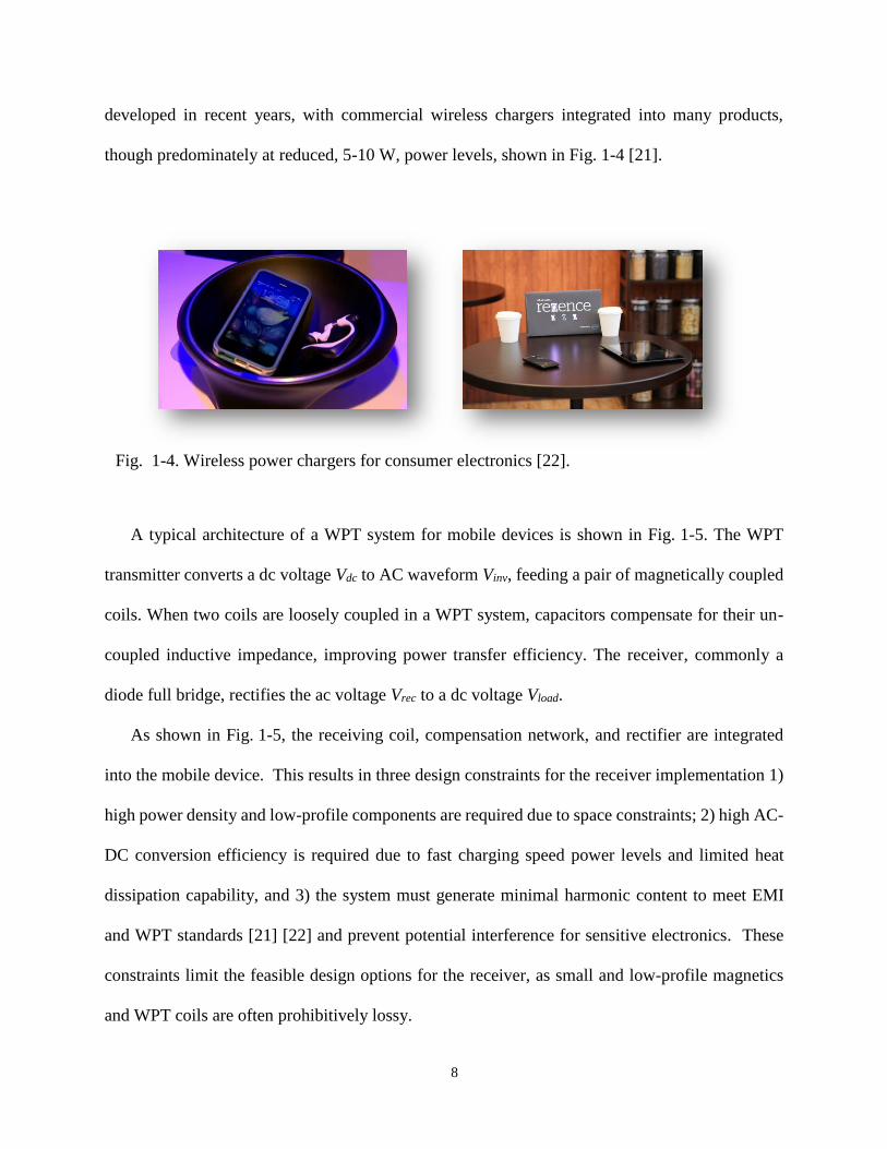
Fig. 1-4. Wireless power chargers for consumer electronics [22]. ................................................ 8
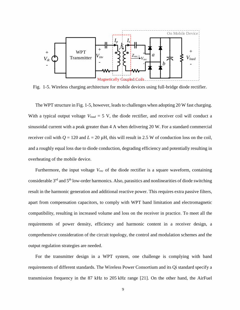
Fig. 1-5. Wireless charging architecture for mobile devices using full-bridge diode rectifier. ..... 9
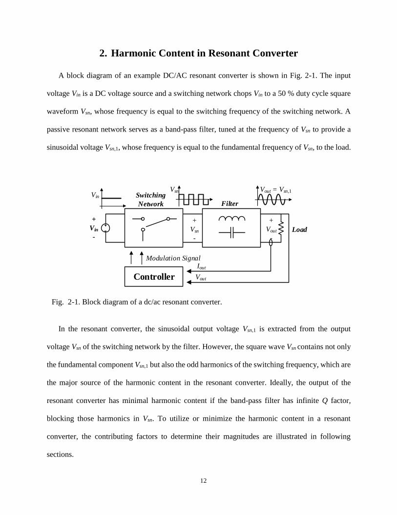
Fig. 2-1. Block diagram of a dc/ac resonant converter. ............................................................... 12
Fig. 2-2. (a) Ideal resonant tank response and zero current harmonics; (b) Non-ideal resonant tank
response and leaked current harmonics. ....................................................................................... 14
Fig. 2-3. (a) Carrier-based pulse width modulation; (b) Carrier-based PWM spectrum. ............ 15
Fig. 2-4. Carrier-based PWM for dual frequency modulation with 11 equivalent switching angles.
(a) time domain waveforms; (b) frequency domain spectrum. ..................................................... 16
Fig. 2-5. Space vectors in a three-phase full bridge system. ........................................................ 17
Fig. 2-6. (a) Programmed pulse width modulation (SHE); (b) Programmed PWM spectrum. ... 18
Fig. 2-7. (a) Frequency modulation; (b) Pulse density modulation; (c) Duty cycle modulation. 20
Fig. 3-1. (a) Unipolar programmed PWM waveform; (b) Bipolar programmed PWM waveform.
....................................................................................................................................................... 27
Fig. 3-2. (a) Separate converter configuration for dual-frequency generations; (b) Corresponding
spectrum of separate converter configuration. .............................................................................. 32
Fig. 3-3. Shared phase-leg configuration for dual-frequency generation. (a) Schematic circuit; (b)
Spectrum. ...................................................................................................................................... 34
Fig. 3-4. Carrier-based PWM scheme for dual-frequency generation; (a) Schematic circuit; (b)
Spectrum. ...................................................................................................................................... 36
Fig. 4-1. A full bridge inverter. Input voltage Vdc, output voltage Vab. ........................................ 39
Fig. 4-2. Square waveform and its spectrum at different duty ratio. 50% duty cycle waveform (a)
and spectrum (b); 27% duty ratio waveform (c) and spectrum (d); 5% duty ratio waveform (e) and
spectrum (f); .................................................................................................................................. 41
Fig. 4-3. Carrier-based PWM waveform and its spectrum at different duty ratio. Rmod = 3 waveform
(a) and spectrum (b); Rmod = 5 waveform (c) and spectrum (d); Rmod = 7 (e) and spectrum (f); .. 43

xiii
Fig. 4-4. SHE waveform and its spectrum at different duty ratio. 3-switching-angle waveform (a)
and spectrum (b); 5-switching-angle waveform (c) and spectrum (d); 7-switching-angle waveform
(e) and spectrum (f);...................................................................................................................... 45
Fig. 4-5. SHE modulation range. (a) 3-switching-angle case; (b) 5-switching-angle (c) 7-
switching-angle. ............................................................................................................................ 46
Fig. 4-6. Quarter-wave symmetry, unipolar MFPWM formulation. ............................................ 50
Fig. 4-7. Unipolar MFPWM 5-switching-angle case. (a) Time domain waveforms; (b) Frequency
domain spectrum; (c) Modulation range of HF element when Mi(LF) = 0.6. ................................. 53
Fig. 4-8. Quarter-wave symmetry, bipolar MFPWM formulation. .............................................. 54
Fig. 4-9. Bipolar MFPWM 5-switching-angle case. (a) Time domain waveforms (b) Frequency
domain spectrum. (c) Modulation range of HF element when Mi(LF) = 0.6. ................................. 55
Fig. 4-10. Quarter-wave symmetry, phase-shift MFPWM formulation. ..................................... 56
Fig. 4-11. (a) Normalized Bipolar MFPWM waveforms. (b)Derivation of normalized phase shift
MFPWM waveforms. ................................................................................................................... 57
Fig. 4-12. Phase shift 5-switching-angle MFPWM. (a) Time domain waveforms (Mi(LF) = 0.6,
Mi(HF) = 0.5); (b) Frequency domain spectrum. (c) Switching angles vs. HF modulation range.. 59
Fig. 4-13. Unipolar waveform boundaries. LF bottom boundary waveforms (a) and spectrum (b);
LF top boundary waveforms (c) and spectrum (d). ...................................................................... 63
Fig. 4-14. Unipolar waveform and MFPWM waveforms. HF top boundary waveforms (a) and
spectrum (b) in a unipolar waveform; HF top boundary waveforms (c) and spectrum (d) in a
MFPWM waveform. ..................................................................................................................... 64
Fig. 4-15. Bipolar waveform boundaries. LF top boundary waveforms (a) and spectrum (b); HF
top boundary waveforms (c) and spectrum (d). ............................................................................ 66
Fig. 4-16. Relationship between LF modulation index MiLF and HF modulation range MiHF for
unipolar, phase shift and bipolar MFPWM. (a) 5-switching-angle case (b) 7-switching-angle case.
....................................................................................................................................................... 67
Fig. 4-17. Bipolar MFPWM with normalized amplitude (VLF = 0.5, VHF = 0.9). (a) time domain
waveforms. (b) Spectrum. (c) Switching angle solution............................................................... 73
Fig. 4-18. Unipolar MFPWM with normalized amplitude (VLF = 0.6, VHF = 0.34). (a) time domain
waveforms. (b) Spectrum. (c) Switching angle solution............................................................... 74
xiv
Fig. 4-19. Bipolar MFPWM with normalized amplitude (Fundamental = 0, VLF = VHF = 0.6Vdc).
(a) time domain waveforms. (b) Spectrum. (c) Switching angle solution when Fundamental = 0,
VLF = 0.6Vdc. .................................................................................................................................. 77
Fig. 4-20. Unipolar MFPWM with normalized amplitude for narrowband dual-mode WPT
(Fundamental = 0.6Vdc, VLF = VHF = 0.35Vdc). (a) time domain waveforms. (b) Spectrum. (c)
Switching angle solution when Fundamental = 0.6Vdc, VLF = 0.35Vdc. ........................................ 78
Fig. 4-21. Multilevel waveforms of MFPWM [61]. .................................................................... 79
Fig. 4-22. Multiple solutions for phase-shift MFWPM with 3 switching angles per quarter-wave;
Solution 1 waveform (a), spectrum(c) and the solution range(e); Solution 2 waveform (b),
spectrum(d) and the solution range(f); .......................................................................................... 82
Fig. 4-23. Multiple solutions for phase-shift MFWPM with 5 switching angles per quarter-wave;
Solution 1 waveform (a), spectrum(c) and the solution range(e); Solution 2 waveform (b),
spectrum(d) and the solution range(f); .......................................................................................... 83
Fig. 5-1. An ultrasonic and radio frequency combined electrosurgical power supply. ............... 86
Fig. 5-2. Block diagram of multi-mode ESG. .............................................................................. 87
Fig. 5-3. Multi-mode ESG use DC/DC pre-regulation to extend RF output range. .................... 88
Fig. 5-4. Simulation waveforms of multi-mode ESG. (a) Time domain waveform; (b) Spectrum.
....................................................................................................................................................... 89
Fig. 5-5. (a) Schematic circuits of multi-mode ESG using MFPWM; (b) Hardware platform. .. 91
Fig. 5-6. (a) 5SA Phase-shift MFPWM voltage waveforms (VLF = 0.6, VHF = 0.5, five-switching-
angle case). (b) Spectrum of inverter output voltage. ................................................................... 92
Fig. 5-7. (a) 5SA Bipolar MFPWM voltage waveforms (VLF = 0.6, VHF = 0.5, five-switching-angle
case). (c) Spectrum of inverter output voltage. ............................................................................. 92
Fig. 5-8. (a) 5SA Unipolar MFPWM voltage waveforms (VLF = 0.6, VHF = 0.5, five-switching-
angle case). (b) Spectrum of inverter output voltage. ................................................................... 92
Fig. 5-9. (a) Phase-shift DFSHE voltage waveforms (VLF = 0.6, VHF = 0.5, 7-switching-angle case).
(b) FFT analysis from oscilloscope. .............................................................................................. 93
Fig. 5-10. (a) Schematic circuit of proposed dual-frequency WPT system. (b) Simplified circuit
model in dual-frequency mode. .................................................................................................... 96
Fig. 5-11. (a) Simplified circuit model using superposition method. (b) voltage gains of two
channels. (k1 = k2 = 0.1). ............................................................................................................... 97
xv
Fig. 5-12. Multi-receiver WPT using MFPWM for Qi frequency band. ..................................... 99
Fig. 5-13. (a) Equivalent simplified circuit model for narrowband dual-mode WPT. (b) Voltage
gains of two channels. (k = 0.1) .................................................................................................. 101
Fig. 5-14. Experimental Setup for the proposed single-inverter dual-mode WPT system. ....... 104
Fig. 5-15. Wideband dual-mode 101.2 kHz/6.78 MHz using bipolar MFPWM: VLF = 0.5,
VHF = 0.9 (normalized). (a) Inverter output voltage and its spectrum when Vdc =20 V. (b) Inverter
output, 101. 2 kHz load voltage, 6.78 MHz load voltage when Vdc =20 V. (c) 6.78 MHz load
voltage and its spectrum when Vdc =10 V. .................................................................................. 105
Fig. 5-16. Wideband dual-mode 101.2 kHz/6.78 MHz using bipolar MFPWM: VLF = VHF = 0.6
(normalized). (a) Inverter output voltage and its spectrum when Vdc =10 V. (b) Inverter output,
101. 2 kHz load voltage, 6.78 MHz load voltage when Vdc =10 V. (c) 6.78 MHz load voltage and
its spectrum when Vdc =10 V. ..................................................................................................... 106
Fig. 5-17. Wideband dual-mode 205.5 kHz/6.78 MHz using bipolar MFPWM: VLF = 0.5, VHF
= 0.9 (normalized). (a) Inverter output voltage and its spectrum when Vdc =25 V. (b) Inverter output,
205.5 kHz load voltage, 6.78 MHz load voltage Vdc =25 V. (c) 6.78 MHz load voltage and its
spectrum when Vdc = 10 V. ......................................................................................................... 108
Fig. 5-18. Wideband dual-mode 101.2 kHz/6.78 MHz using unipolar MFPWM: VLF = 0.6, VHF
= 0.34 (normalized). (a) Inverter output voltage and its spectrum when Vdc =25 V. (b) Inverter
output, 101. 2 kHz load voltage, 6.78 MHz load voltage Vdc =25 V. (c) 6.78 MHz load voltage and
its spectrum when Vdc =10 V. ..................................................................................................... 109
Fig. 5-19. Narrowband 87 kHz/205 kHz dual-mode operation: VLF = VHF = 0.6 (normalized) when
Vdc =25 V. (a) Inverter output voltage waveform and its spectrum. (b) Inverter output, 87 kHz load
voltage, 205 kHz load voltages. .................................................................................................. 110
Fig. 5-20. Dual-mode WPT system dc-to-load efficiency curves. ............................................ 113
Fig. 5-21. (a) Measured device case temperature and device losses. (b) Transmitter efficiency
estimation curve based-on thermal resistances. .......................................................................... 113
Fig. 6-1. Typical wireless charging architecture for mobile devices. ........................................ 116
Fig. 6-2. Equivalent circuit of WPT system. ............................................................................. 119
Fig. 6-3. Diode bridge rectifier for WPT receiver. .................................................................... 120
Fig. 6-4. Voltage gain curve with a diode rectifier. ................................................................... 121
xvi
Fig. 6-5. Relationship between rectifier impedance and transmitter current (red circle line),
receiver current (blue square line), and system efficiency (magenta cross line) at 20W. .......... 122
Fig. 6-6. Diode bridge rectifier plus Buck converter for WPT receiver. .................................. 123
Fig. 6-7. Voltage gain curve with a diode rectifier plus 3:1 step-down Buck converter. .......... 125
Fig. 6-8. Relationship between dc/dc duty cycle d and transmitter current (red circle line); receiver
current (blue square line); and rectifier impedance (magenta cross line). .................................. 125
Fig. 6-9. Synchronous Rectifier Plus 3:1 Ladder Switched-Capacitor DC/DC Converter. ...... 126
Fig. 6-10. Voltage gain curve with a synchronous rectifier plus 3:1 switched-capacitor DC/DC
Converter..................................................................................................................................... 127
Fig. 6-11. 7-level switched-capacitor ac-dc rectifier with 3:1 voltage step-down. .................... 128
Fig. 6-12. Control signal sequence for 7-level SC rectifier in a half cycle of input waveform. Solid
line: high side switch and charge sharing switch (S1AH, S2AH, S3AH, SC1A, SC2A); dash line: low side
switch (S1AL, S2AL, S3AL). .............................................................................................................. 130
Fig. 6-13. Operation of step-down MSC rectifier in one half-cycle. Operation sequence1-2-3-4-3-
2-1. (a) Subinterval 1; (b) Subinterval 2; (c) Subinterval 3; (d) Subinterval 4. .......................... 131
Fig. 6-14. Impedance transformation using MSC step-down rectifier for a WPT system. ....... 132
Fig. 6-15. Voltage gain curve with a 7-level step-down switched capacitor ac-dc rectifier, m = 2.5
and Rload = 1.25 Ω. ...................................................................................................................... 134
Fig. 6-16. Relationship between modulation index m and transmitter current (red circle line);
receiver current (blue square line); and rectifier impedance (magenta cross line). .................... 134
Fig. 6-17. Relationship between modulation index m and the dc input-to-load voltage gain at 150
kHz, and given load Rload = 1.25 Ω. ............................................................................................ 134
Fig. 6-18. Simulation results using diode rectifier. (a) Schematic circuit; (b) Simulation waveform.
Inverter voltage: Vsource and current: Isource; receiver voltage Vrec and current Irec. ..................... 137
Fig. 6-19. Simulation results using diode rectifier plus Buck converter. (a) Schematic circuit; (b)
Simulation waveform. Inverter voltage: Vsource and current: Isource; receiver voltage Vrec and current
Irec. ............................................................................................................................................... 142
Fig. 6-20. Waveforms of 3:1 Buck converter. IL: inductor current; Vsw: switching node voltage;
Vbus: diode rectifier output; Vload: load voltage. .......................................................................... 142
Fig. 6-21. Efficiency vs. load current curve of a reference Buck converter (Texas Instruments
BQ25910). ................................................................................................................................... 144
xvii
Fig. 6-22. Schematic circuit using synchronous rectifier plus Buck converter. ........................ 146
Fig. 6-23. Simulation results using synchronous rectifier plus 3:1 Ladder switched-capacitor
converter. (a) Schematic circuit; (b) Simulation waveform. Inverter voltage: Vsource and current:
Isource; receiver voltage Vrec and current Irec. ................................................................................ 147
Fig. 6-24. Key waveforms of synchronous rectifier plus 3:1 Ladder SC converter. ................. 148
Fig. 6-25. Model of an idealized 3:1 switched-capacitor converter. [115] ................................ 150
Fig. 6-26. 3:1 Ladder SC converter operation: (a) Subinterval 1; (b) Subinterval 2. [115] ...... 150
Fig. 6-27. Simulation results using 7-level switched capacitor 3:1 step-down ac-dc rectifier. (a)
Schematic circuit; (b) Simulation waveform. Inverter voltage: Vsource and current: Isource; receiver
voltage Vrec and current Irec. ........................................................................................................ 154
Fig. 6-28. Charge sharing loss equivalent circuits in MSC rectifier: capacitor to capacitor. .... 155
Fig. 6-29. Simulation waveforms using stack charge control. Top column: gate signals of high-
side devices; Middle column: Rectifier input voltage and current; Bottom column: Flying capacitor
voltage ripple. ............................................................................................................................. 158
Fig. 6-30. Queue charge control sequence for 7-level MSC rectifier in half line cycle. Solid line:
high side switch and charge sharing switch (S1AH, S2AH, S3AH, SC1A, SC2A); dash line: low side switch
(S1AL, S2AL, S3AL)........................................................................................................................... 160
Fig. 6-31. Simulation waveforms using queue charge control. Top column: gate signals of high-
side devices; Middle column: Rectifier input voltage and current; Bottom column: Flying capacitor
voltage ripple. ............................................................................................................................. 160
Fig. 6-32. Stack and Queue charge control loss vs. input voltage and current phase angle. ..... 161
Fig. 6-33. Simulation results using 7-level SC ac-dc rectifier m = 3.81. Inverter voltage: Vsource
and current: Isource; receiver voltage Vrec and current Irec. ........................................................... 162
Fig. 6-34. (a) WPT system with inverter and rectifier; (b) circuit model for current THD modeling.
..................................................................................................................................................... 166
Fig. 6-35. Spectra of the inverter and the rectifier voltage. ....................................................... 166
Fig. 6-36. Current waveforms and spectrums with diode rectifier (a) Time domain waveforms; (b)
Spectrum of primary and secondary current. .............................................................................. 169
Fig. 6-37. Current waveforms and spectrums with diode rectifier plus 3:1 Buck converter: (a)
Time domain waveforms; (b) Spectrum of primary and secondary current. .............................. 170
xviii
Fig. 6-38. Current waveforms and spectrums with MSC 3:1 step-down rectifier (m = 2.5): (a)
Time domain waveforms; (b) Spectrum of primary and secondary current. .............................. 171
Fig. 6-39. THD minimization approach using MSC rectifier. ................................................... 174
Fig. 6-40. Current THD improvement using sinusoidal inverter & rectifier SHE modulation. (a)
time domain waveforms; (b) current THD. ................................................................................ 175
Fig. 6-41. Current THD improvement using inverter/rectifier SHE modulation. ..................... 176
Fig. 6-42. Schematic circuit of MSC step-up inverter/step-down rectifier using SHE modulation
to improve current THD.............................................................................................................. 177
Fig. 6-43. Current THD improvement using MSC inverter/rectifier SHE modulation. (a) time
domain waveforms; (b) spectra of the currents........................................................................... 177
Fig. 6-44. Current THD performance using MSC inverter/ a diode rectifier plus 3:1 Buck/SC
converter. (a) time domain waveforms; (b) spectra of the currents. ........................................... 178
Fig. 6-45. Current THD performance using MSC inverter/ a diode rectifier. (a) time domain
waveforms; (b) spectra of the currents........................................................................................ 179
Fig. 6-46. Spider chart of four candidates. Note that candidate w/ regulation scores 1 and candidate
w/o regulation scores 0. Other values are normalized based on the highest value in the item. .. 184
Fig. 6-47. Spider chart of four candidates considering thermal area. Note that candidate w/
regulation scores 1 and candidate w/o regulation scores 0. Other values are normalized based on
the highest value in the item. ...................................................................................................... 185
Fig. 7-1. Simulation results using 5-level SC rectifier. (a) Schematic circuit; (b) Simulation
waveforms: Receiver voltage Vrec and current Irec; flying cap voltage Vc1 and output voltage Vout.
..................................................................................................................................................... 188
Fig. 7-2. 5 level SC rectifier sub-circuits. (a) charging state; (b) discharging state. ................. 189
Fig. 7-3. Relationship between output impedance of 5 level SC rectifier and single FET sizing.
..................................................................................................................................................... 191
Fig. 7-4. (a) Relationship between the total loss of the 5 level SC rectifier and total FET area; (b)
The loss distribution when total FET area is 1mm2; (b) The loss distribution when total FET area
is 6 mm2. ..................................................................................................................................... 191
Fig. 7-5. Simulation results using synchronous Rectifier plus 2:1 SC converter. (a) Schematic
circuit; (b) Simulation waveforms: Receiver voltage Vrec and current Irec; flying cap voltage Vc1
and output voltage Vout. ............................................................................................................... 193
xix
Fig. 7-6. 2:1 SC converter sub-circuits. (a) charging state; (b) discharging state. ..................... 194
Fig. 7-7. Relationship between output impedance of 2:1 SC converter and single FET sizing. 195
Fig. 7-8. Relationship between the total loss of the synchronous rectifier plus 2:1 step-down SC
converter and total FET area; (b) The loss distribution when total FET area is 1mm2; (b) The loss
distribution when total FET area is 6 mm2. ................................................................................ 196
Fig. 7-9. 2:1 SC converter sizing. (a) Sizing of flying capacitor and the output impedance; (b)
changes of switching frequency and the output impedance........................................................ 198
Fig. 7-10. Simulation results using 5-level SC rectifier. (a) switching frequency of 150 kHz; (b)
switching frequency of 300 kHz. ................................................................................................ 199
Fig. 7-11. The relationship between total FET area and total loss for two rectifiers @ 150 kHz,
total 4(a)/6(b) 20 µF flying capacitors, 9V, 20W. (a) 5-level SC rectifier & rectifier plus 2:1 SC
converter; (b) rectifier plus 7-level & 3:1 SC converter. ............................................................ 200
Fig. 7-12. Block diagram of output regulation for WPT system. .............................................. 202
Fig. 7-13. (a) Regulation boundary of the WPT system using MSC rectifier; (b)Conduction loss
map associated with regulation boundary (c) Efficiency map associated with regulation boundary.
..................................................................................................................................................... 203
Fig. 7-14. Two-loop control strategy for WPT system. ............................................................. 204
Fig. 7-15. Digital single-integrator compensator design for MSC rectifier. .............................. 205
Fig. 7-16. Modulator design for MSC rectifier. (a) Schematic circuit of MSC rectifier; (b) Block
diagram of carrier-based modulator; (c) Gate signal diagram, ................................................... 207
Fig. 7-17. Closed-loop control simulation with load change 20W to 0.5W @0.1s. (a) output
voltage waveform; (b) voltage and current waveforms of MSC rectifier and inverter. ............. 209
Fig. 7-18. Closed-loop control simulation with input voltage change 10V to 13V @0.1s. (a) output
voltage waveform and input voltage waveform; (b) voltage and current waveforms of MSC
rectifier and inverter. ................................................................................................................... 210
Fig. 7-19. Closed-loop control simulation with output reference change 5V to 6V at 0.1s. ..... 210
Fig. 7-20. System diagram of the prototype control. ................................................................. 211
Fig. 7-21. Proposed WPT system with 7-level MSC prototype (a) system overview; (b) Resonant
tank and module with a 5-Cent Euro. ......................................................................................... 212
xx
Fig. 7-22. (a) 7-level, 20 W MSC rectifier output dc voltage, input staircase voltage and the input
current when modulation index m = 2.5. (b) Input voltage spectrum when using SHE modulation
scheme......................................................................................................................................... 214
Fig. 7-23. Gate driver control signals in one phase leg using queue charge control sequence.. 214
Fig. 7-24. Voltages of flying capacitors C1A, C2A and C3A using queue charge control. ............ 214
Fig. 7-25. (a) WPT system using diode rectifier: inverter current, rectifier input voltage and the
input current at 10W. (b) Diode Rectifier input voltage spectrum. ............................................ 216
Fig. 7-26. Predicted and measured dc-to-dc system efficiency using MSC rectifier m = 2.5 and
diode bridge rectifier. .................................................................................................................. 216
Fig. 7-27. Loss distribution at 20 W of the proposed WPT architecture when m = 2.5. ........... 216
Fig. 7-28. Predicted and measured dc-to-dc system efficiency using MSC rectifier m = 3.81. 218
Fig. 7-29. Predicted and measured dc-to-dc system efficiency by sweeping modulation index m at
fixed power of 20W, and the relationship between modulation index m and rectifier impedance.
..................................................................................................................................................... 218
Fig. 7-30. Experimental results of current waveforms and spectrum. Inverter: 50% duty cycle
square voltage; rectifier: m = 2.5 SHE 7-level staircase waveform. (a) voltage and current
waveforms of inverter and rectifier; (b) inverter current spectrum;(c) rectifier current spectrum.
..................................................................................................................................................... 220
Fig. 7-31. Experimental results of current waveforms and spectrum. Inverter: 50% duty cycle
square voltage; rectifier: m = 3.81 square waveform. (a) voltage and current waveforms of inverter
and rectifier; (b) inverter current spectrum;(c) rectifier current spectrum. ................................. 222
Fig. 7-32. Experimental results of current waveforms and spectrum. Inverter: m = 1 SHE unipolar
voltage; rectifier: m = 2.5 seven-level staircase waveform. (a) voltage and current waveforms of
inverter and rectifier; (b) inverter current spectrum;(c) rectifier current spectrum. ................... 223
Fig. 7-33. Measured efficiency curve comparison..................................................................... 225
Fig. 7-34. Open-loop tests of carrier-based multilevel modulator. (a) m = 2.2; (b) m = 2.9; (c) m
=3.7. ............................................................................................................................................ 227
Fig. 7-35. Input voltage step change: input voltage changes from 13V to 15V. ....................... 228
Fig. 7-36. Zoomed-in waveforms of input voltage step change. (a) Input voltage = 10V;(b) Input
voltage = 9V. ............................................................................................................................... 228
Fig. 7-37. Load step change: load changes from 13W to 6W.................................................... 229
xxi
Fig. A-1. GaN system GS66508P Eon and Eoff curves. (Test condition: Vdc = 400V, room
temperature. Vgs_on=7V and Vgs_off=0V). ..................................................................................... 246
Fig. A-2. Relationship between Rds(on) and junction temperature (GS66508T). ........................ 247
Fig. A-3. Relationship between switching energy Eon and the junction temperature [106]. ..... 249
Fig. A-4. Reverse conduction characteristic of selected E-mode GaN (Vgs_off = 0V). ............... 249
Fig. A-5. Additional Cgs1 to mitigate cross talk issue (Vgs_on = 7V, Vgs_off = 0V). ...................... 251
Fig. A-6. Separate turn-on and turn-off gate resistance to mitigate cross talk issue (Vgs_on = 7V,
Vgs_off = 0V). ................................................................................................................................ 251
Fig. A-7. Different Cgs1 and capacitive loss in a phase leg configuration (Rg = 0 Ω). ............. 253
Fig. A-8. Comparison between additional Cgs solution and two-drive path solution in a phase leg
configuration. .............................................................................................................................. 253
Fig. A-9. (a) Heatsink and thermal interface design for GaN device. (b) Gate drive PCB layout.
..................................................................................................................................................... 254
Fig. A-10. (a) Prototype picture. (b) FEA thermal analysis for the individual components. (c)
enclosure top surface, and (d) enclosure bottom surface. ........................................................... 255
1
1. Introduction
40 % energy of US now is directly consumed in terms of the electricity [1][2], and it frequently
requires an electrical conversion between the DC and the AC with varying amplitudes and
frequencies (in AC), as the end-users require a variety of electrical power sources for a wide range
of applications, from a 5 W mobile phone DC battery charger to a 1 MW three-phase AC motor
drive. To address such a wide range of electrical conversion applications, the concept of power
electronics emerged to meet such demands since the year of 1902 when the first mercury arc valve,
a chemical/mechanical switch, was invented to convert the grid AC voltage to a DC voltage.
The conversion efficiency of electrical energy has substantially improved during past decades,
as the semiconductor switches and modern power electronics technologies evolve. Unlike a linear
power regulator where the semiconductor switches work in the linear region and therefore causing
high energy dissipation, the modern high-efficiency power converters often operate in a switched
manner, reducing energy dissipation on semiconductor switches. In consequence, such power
converters are also called switched mode power supplies (SMPS).
out
in
P
P (1-1)
outP
V (1-2)
The conversion efficiency η of a power converter is a critical design metric, defined as the ratio
of the output power Pout to the input power Pin of the power converter. An increase of conversion
efficiency saves enormous energy losses and greenhouse gas emission, producing significant
economic profits to a world that consume 20.9 PWh electricity in 2012 [2]. Another key metric is
the power density α, defined in (1-2), where V is the volume of power converters. The reduced size
decreases the costs of manufacturing, transportation, and installation, which enables the spread of
2
distributed energy interfaces [3]. For electric vehicles, ships and aircraft, shrinking the size of the
power systems leaves additional space for passengers and cargo and often yields a corresponding
decrease in weight and increase in fuel efficiency [4].
A power converter consists of the switched-mode semiconductors, passive filtering
components, e.g. capacitors and inductors. An ideal converter is assumed to achieve 100 % energy
conversion efficiency with zero volume, i.e. an infinite power density. However, a realistic one
always has power losses on its components. The loss mechanisms on the semiconductor device
belong to one of two categories. Conduction loss results from a small resistance of on-state devices
when a current flows through them. Switching loss is caused by the overlap of a non-zero voltage
across the device and a non-zero current flowing through it during the switching transitions. The
power density of a real converter is finite as well, and its major volume includes the devices and
the attached heatsink due to the heat dissipation requirement, the passive filters, and other auxiliary
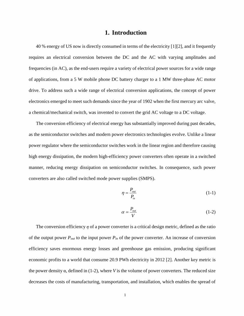
circuits. A 97 % efficiency, 102 W/in3 power density, 2 kVA single-phase DC-to-AC converter is
shown in Fig. 1-1. The heatsink and the output passive filters, take almost half of the total volume
of the prototype [5].
Fig. 1-1. 2 kVA single-phase DC-to-AC power converter prototype.
3
One popular way to reduce the size of the passive filters is to increase the switching frequency
of the semiconductor devices. Smaller filtering components can then be employed, as the corner
frequency of the output filter increases with the switching frequency [6]. However, at higher
switching frequency the semiconductor devices will have, higher switching loss if the loss is not
alleviated with additional design efforts, and this substantially decreases the efficiency and
requires a larger heatsink into the converter.
To achieve a high-efficiency and high-power-density design of power converters, one
promising candidate, the resonant converter, has received an increasing interest in the power
electronics research. The resonant converter operating mode facilitates soft switching, i.e. a
substantial reduction of the switching losses, of the semiconductor devices at high switching
frequency, In consequence, the switching frequency of the resonant converter can increase to tens
of megahertz with considerably low switching losses, resulting in a reduced size of the output
filters, and a smaller heatsink if assuming a constant conduction loss.
The resonant converter, in general, has potential to achieve high power density while
maintaining a high efficiency. Those advantages of the resonant converters drive an increased
demand from many industrial and consumer applications, such as electrosurgical power supplies,
wireless power transfer systems, and induction heating, which enables new technologies and
facilitates our lives. Many applications of resonant converters share similar requirements, i.e. the
development of combined functionality with reduced hardware, and the “noise” suppression to
comply with specific design standards or safety concerns. This dissertation focuses on these topics
in resonant converter design from a modulation and control perspective. Two representative
applications of the resonant converters, electrosurgical power supplies and wireless power transfer,

4
are investigated to reveal opportunities and challenges by applying the proposed multi-frequency
modulation and control.
1.1 Applications of Resonant Converters
Resonant converters are one type of switched-mode power supplies, where a resonant
impedance network (also called resonant tank), e.g. an inductor and a capacitor in series, and tuned
at a specific operating frequency. The current and voltage waveforms in the resonant tank are
approximately sinusoidal, and the magnitude of those current and voltage are large compared with
traditional pulse width modulated (PWM) switched mode converters [7]-[12].
Assuming an infinite quality factor (or Q factor) of the resonant tank, it serves as an ideal band-
pass filter that only allows the resonant frequency to pass. Therefore, the resonant frequency
dominates, and other frequencies are often ignored at the output. If closely examining the spectrum
of a non-ideal resonant converter, however, not only the resonant frequency, but also many other
frequencies, such as low-order harmonics, or sideband harmonics, appear at the output, with
different magnitudes. The quality factor of the resonant tank is finite, and the band-pass filter has
limited attenuation on those frequencies.
The existence of harmonics in a resonant converter is inevitable in practical applications, and
the cause of harmonic generations and contributing factors are further investigated in Chapter 2.
Those harmonics are unwelcome in many applications. On the other hand, their existence is
potentially beneficial for some scenarios. It motivates us to investigate an intelligent approach to
harness the harmonic content in the resonant converter. In the following sections, some application
backgrounds of the resonant converters are introduced to provide a clear understanding of the
needs for harmonic content control.

5
1.1.1 Electrosurgical Power Supply
Electrosurgery is the application of high-frequency AC electrical current to conduct surgery.
Compared with the traditional scalpel-based surgery, electrosurgery can achieve a precise cutting
depth with limited blood loss, which stimulates a billion-dollar market [13]. One key component
in electrosurgery is the electrosurgical power supply, also called electrosurgical units/generators
(ESG) [14]. As ESG is an electronic device that generates a high-frequency AC current to raise
the intracellular temperature to achieve the vaporization of the human tissues or the combination
of desiccation and coagulation on tissue cells. Desiccation is the procedure that dries tissue cells,
and coagulation is the process that blood turns from a liquid to a gel-form blood clot. Those effects
can be translated into cutting or sealing of the human tissues in traditional surgery [14]-[20].
In the electrosurgery, a ESG directly uses the patients’ tissue as a current path, and the
frequency, amplitude, and energy density of the generated AC current determines the surgical
performance, such as the cutting depth, or the coagulation rate. For example, a low-magnitude,
low-frequency continuous AC current is used for “cut” function in ESG, while a high-amplitude,
high-frequency pulsed AC current is used for the “coagulation” purposes [20]. In Fig. 1-2, an
ultrasonic (US) dissection instrument, usually is tuned in 20 kHz - 50 kHz, employs a low-
frequency AC current to produce mechanical friction which creates heat allowing dissection of the
human tissue. An instrument of desiccation and coagulation is usually powered by a radio-
frequency (RF) AC current within 200 kHz – 3.3 MHz [17], and performs dissection through direct
electrical conduction through tissue.
US and RF AC currents, in conventional solutions, are separately generated from multiple
resonant converters, leading to a multi-ESG configuration. For advanced electrosurgery, a
concurrent generation of blended AC currents, at different frequencies and amplitudes, is

6
advantageous for improved surgecial performance, e.g. the simultaneous cutting and coagulation
to reduce bleeding and patients’ pain. Moreover, the multi-source ESG provides surgeons with a
flexibility to switch between the US and the RF instruments, depending on the specific tissue and
surgeons’ preferences. This demand essentially requires that a single ESG can modulate and
control multiple AC currents from a single generator. Another benefit is to save ESG costs and
space in the surgery room.
One top priority of ESGs is the patients’ safety, and a key metric is the magnitudes of the
leakage currents of the ESGs, which result from the harmonic content in the resonant converters.
If an excessive presence of those harmonics leaks from the converters, they are likely to result in
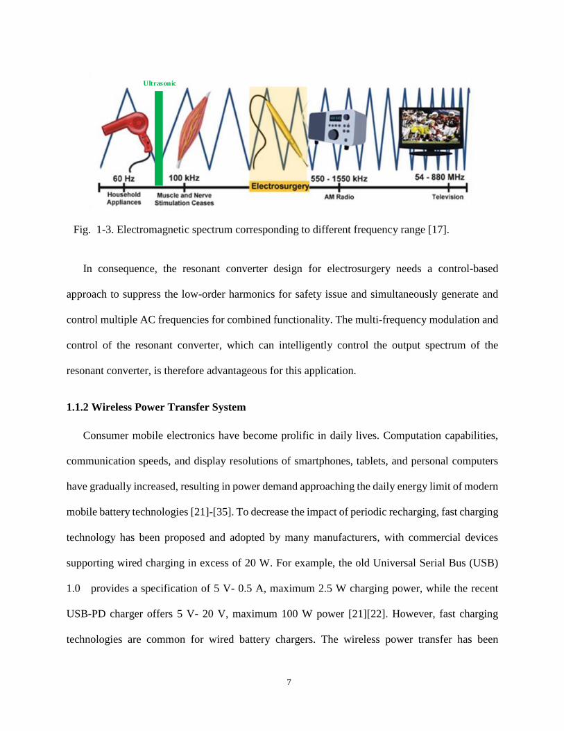
muscle contraction and patient pain [17], as human muscles and nerves are very sensitive to AC
frequencies below 100 kHz, shown in Fig. 1-3.
Therefore, any frequency that is produced from the resonant converter must be well-attenuated
below safety limits. Those sub-100 kHz AC frequencies in ESGs are usually the low-order and the
sideband harmonics from the modulations of the resonant converters. Traditionally, a designated
bulky filter is added at the ESG output to limit the leakage currents, leading to an increase of the
total volume, which is burdensome in operating room.
(a) (b)
Fig. 1-2. (a) Ultrasonic instrument. (b) RF instrument. (Pictures by courtesy from Covidien.)
7
In consequence, the resonant converter design for electrosurgery needs a control-based
approach to suppress the low-order harmonics for safety issue and simultaneously generate and
control multiple AC frequencies for combined functionality. The multi-frequency modulation and
control of the resonant converter, which can intelligently control the output spectrum of the
resonant converter, is therefore advantageous for this application.
1.1.2 Wireless Power Transfer System
Consumer mobile electronics have become prolific in daily lives. Computation capabilities,
communication speeds, and display resolutions of smartphones, tablets, and personal computers
have gradually increased, resulting in power demand approaching the daily energy limit of modern
mobile battery technologies [21]-[35]. To decrease the impact of periodic recharging, fast charging
technology has been proposed and adopted by many manufacturers, with commercial devices
supporting wired charging in excess of 20 W. For example, the old Universal Serial Bus (USB)
1.0 provides a specification of 5 V- 0.5 A, maximum 2.5 W charging power, while the recent
USB-PD charger offers 5 V- 20 V, maximum 100 W power [21][22]. However, fast charging
technologies are common for wired battery chargers. The wireless power transfer has been
Ultrasonic
Fig. 1-3. Electromagnetic spectrum corresponding to different frequency range [17].
8
developed in recent years, with commercial wireless chargers integrated into many products,
though predominately at reduced, 5-10 W, power levels, shown in Fig. 1-4 [21].
A typical architecture of a WPT system for mobile devices is shown in Fig. 1-5. The WPT
transmitter converts a dc voltage Vdc to AC waveform Vinv, feeding a pair of magnetically coupled
coils. When two coils are loosely coupled in a WPT system, capacitors compensate for their un-
coupled inductive impedance, improving power transfer efficiency. The receiver, commonly a
diode full bridge, rectifies the ac voltage Vrec to a dc voltage Vload.
As shown in Fig. 1-5, the receiving coil, compensation network, and rectifier are integrated
into the mobile device. This results in three design constraints for the receiver implementation 1)
high power density and low-profile components are required due to space constraints; 2) high AC-
DC conversion efficiency is required due to fast charging speed power levels and limited heat
dissipation capability, and 3) the system must generate minimal harmonic content to meet EMI
and WPT standards [21] [22] and prevent potential interference for sensitive electronics. These
constraints limit the feasible design options for the receiver, as small and low-profile magnetics
and WPT coils are often prohibitively lossy.
Fig. 1-4. Wireless power chargers for consumer electronics [22].
9
The WPT structure in Fig. 1-5, however, leads to challenges when adopting 20 W fast charging.
With a typical output voltage Vload = 5 V, the diode rectifier, and receiver coil will conduct a
sinusoidal current with a peak greater than 4 A when delivering 20 W. For a standard commercial
receiver coil with Q = 120 and L = 20 µH, this will result in 2.5 W of conduction loss on the coil,
and a roughly equal loss due to diode conduction, degrading efficiency and potentially resulting in
overheating of the mobile device.
Furthermore, the input voltage Vrec of the diode rectifier is a square waveform, containing
considerable 3rd and 5th low-order harmonics. Also, parasitics and nonlinearities of diode switching
result in the harmonic generation and additional reactive power. This requires extra passive filters,
apart from compensation capacitors, to comply with WPT band limitation and electromagnetic
compatibility, resulting in increased volume and loss on the receiver in practice. To meet all the
requirements of power density, efficiency and harmonic content in a receiver design, a
comprehensive consideration of the circuit topology, the control and modulation schemes and the
output regulation strategies are needed.
For the transmitter design in a WPT system, one challenge is complying with band
requirements of different standards. The Wireless Power Consortium and its Qi standard specify a
transmission frequency in the 87 kHz to 205 kHz range [21]. On the other hand, the AirFuel
* *
kWPT
Transmitter
On Mobile Device
+
Vload
-
Ip Is
Zrec,1 a
b
+
Vrec
-
+
Vdc
-
+
Vinv
-
Magnetically Coupled Coils
Fig. 1-5. Wireless charging architecture for mobile devices using full-bridge diode rectifier.

10
Alliance, a merger between A4WP and PMA standards, employs the ISM frequency band within
6.78MHz ± 15 kHz [22], and a low band of 100 kHz to 300 kHz. These conflicting standards result
in inconvenience for consumers and manufacturers. Devices with wireless charging capability
designed to different standards are not interoperable, potentially requiring users with multiple
mobile electronic devices to purchase and maintain one charger per device. As a result, a WPT
transmitter that operates in multiple frequency bands, across multiple WPT standards, is attractive.
For either Qi or Airfuel, the allowable frequency band is narrow, where the low-order
harmonics such as the 3rd and the 5th harmonic can easily be beyond their allowable bands.
Generally, bulky passive filters also are added to attenuate them below limitations, and this
solution adds footprint and volume for the transmitter as well. Therefore, a solution that can
suppress those harmonics from generation by the multi-frequency modulation and control, without
adding extra components, is promising to leverage this problem.
1.2 Summary
Resonant converters have received an increased popularity as a promising candidate for high-
efficiency and high-power density power converter designs, which are widely adopted in many
industrial and consumer applications. From the above discussion, the harmonic content is often
regarded as an undesired byproduct of the resonant converter, requiring extra efforts (e.g. bulky
passive filters) to exclude them from the system. This work attempts an intelligent manipulation
of those harmonics to re-utilize or suppresses them from a modulation and control perspective,
comprehensively considering the efficiency and the power density. This exploration will
demonstrate that the multi-frequency modulation and control of the resonant converter provides
additional benefits (i.e. the improvement of cost, efficiency and power density or the total

11
harmonic distortion) on a single metric or the combined performance than the conventional
solutions for two applications, electrosurgical power supplies and wireless power transfer systems.
12
2. Harmonic Content in Resonant Converter
A block diagram of an example DC/AC resonant converter is shown in Fig. 2-1. The input
voltage Vin is a DC voltage source and a switching network chops Vin to a 50 % duty cycle square
waveform Vsn, whose frequency is equal to the switching frequency of the switching network. A
passive resonant network serves as a band-pass filter, tuned at the frequency of Vsn to provide a
sinusoidal voltage Vsn,1, whose frequency is equal to the fundamental frequency of Vsn, to the load.
In the resonant converter, the sinusoidal output voltage Vsn,1 is extracted from the output
voltage Vsn of the switching network by the filter. However, the square wave Vsn contains not only
the fundamental component Vsn,1 but also the odd harmonics of the switching frequency, which are
the major source of the harmonic content in the resonant converter. Ideally, the output of the
resonant converter has minimal harmonic content if the band-pass filter has infinite Q factor,
blocking those harmonics in Vsn. To utilize or minimize the harmonic content in a resonant
converter, the contributing factors to determine their magnitudes are illustrated in following
sections.
Controller
Iout
Vout
+
Vin
-Load
Filter
Switching
Network
Vsn Vout = Vsn,1Vin
Modulation Signal
+
Vsn
-
+
Vout
-
Fig. 2-1. Block diagram of a dc/ac resonant converter.
13
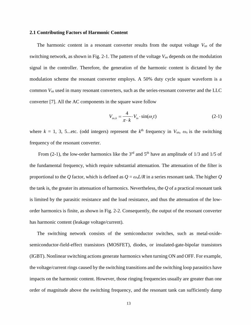
2.1 Contributing Factors of Harmonic Content
The harmonic content in a resonant converter results from the output voltage Vsn of the
switching network, as shown in Fig. 2-1. The pattern of the voltage Vsn depends on the modulation
signal in the controller. Therefore, the generation of the harmonic content is dictated by the
modulation scheme the resonant converter employs. A 50% duty cycle square waveform is a
common Vsn used in many resonant converters, such as the series-resonant converter and the LLC
converter [7]. All the AC components in the square wave follow
,
4sin( )sn k in sV V t
k
(2-1)
where k = 1, 3, 5...etc. (odd integers) represent the kth frequency in Vsn, ωs is the switching
frequency of the resonant converter.
From (2-1), the low-order harmonics like the 3rd and 5th have an amplitude of 1/3 and 1/5 of
the fundamental frequency, which require substantial attenuation. The attenuation of the filter is
proportional to the Q factor, which is defined as Q = ωsL/R in a series resonant tank. The higher Q
the tank is, the greater its attenuation of harmonics. Nevertheless, the Q of a practical resonant tank
is limited by the parasitic resistance and the load resistance, and thus the attenuation of the low-
order harmonics is finite, as shown in Fig. 2-2. Consequently, the output of the resonant converter
has harmonic content (leakage voltage/current).
The switching network consists of the semiconductor switches, such as metal-oxide-
semiconductor-field-effect transistors (MOSFET), diodes, or insulated-gate-bipolar transistors
(IGBT). Nonlinear switching actions generate harmonics when turning ON and OFF. For example,
the voltage/current rings caused by the switching transitions and the switching loop parasitics have
impacts on the harmonic content. However, those ringing frequencies usually are greater than one
order of magnitude above the switching frequency, and the resonant tank can sufficiently damp
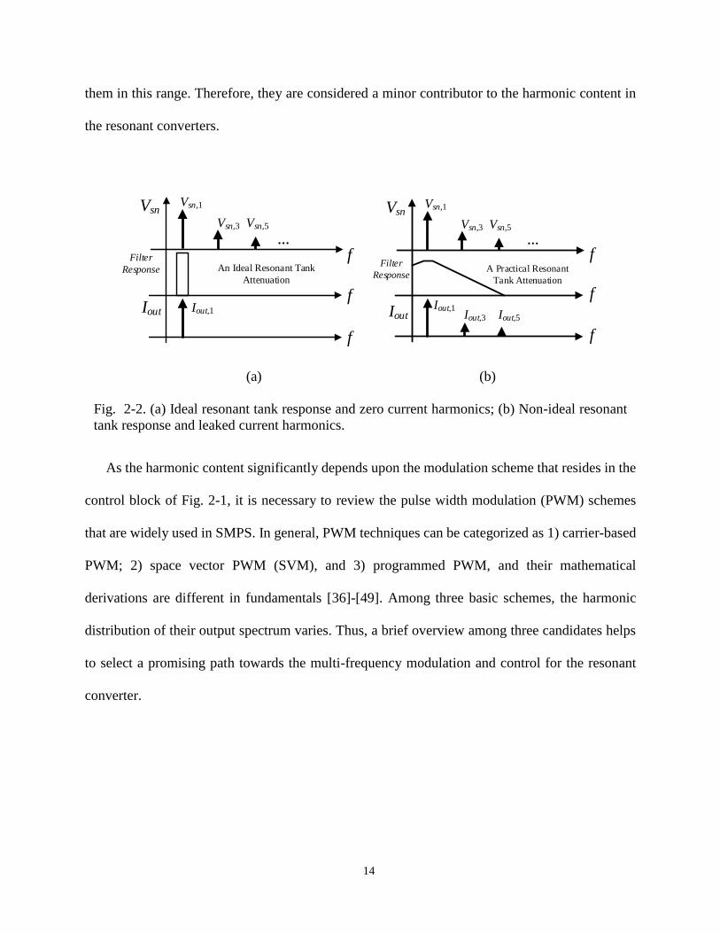
14
them in this range. Therefore, they are considered a minor contributor to the harmonic content in
the resonant converters.
As the harmonic content significantly depends upon the modulation scheme that resides in the
control block of Fig. 2-1, it is necessary to review the pulse width modulation (PWM) schemes
that are widely used in SMPS. In general, PWM techniques can be categorized as 1) carrier-based
PWM; 2) space vector PWM (SVM), and 3) programmed PWM, and their mathematical
derivations are different in fundamentals [36]-[49]. Among three basic schemes, the harmonic
distribution of their output spectrum varies. Thus, a brief overview among three candidates helps
to select a promising path towards the multi-frequency modulation and control for the resonant
converter.
f
VsnVsn,1
Iout,1
An Ideal Resonant Tank
Attenuation
Iout
f
f
...Vsn,3 Vsn,5
Filter
Response
Vsn
f
f
f
...
Filter
Response
Vsn,1
Vsn,3 Vsn,5
Iout,1Iout
A Practical Resonant
Tank Attenuation
Iout,3 Iout,5
(a) (b)
Fig. 2-2. (a) Ideal resonant tank response and zero current harmonics; (b) Non-ideal resonant
tank response and leaked current harmonics.
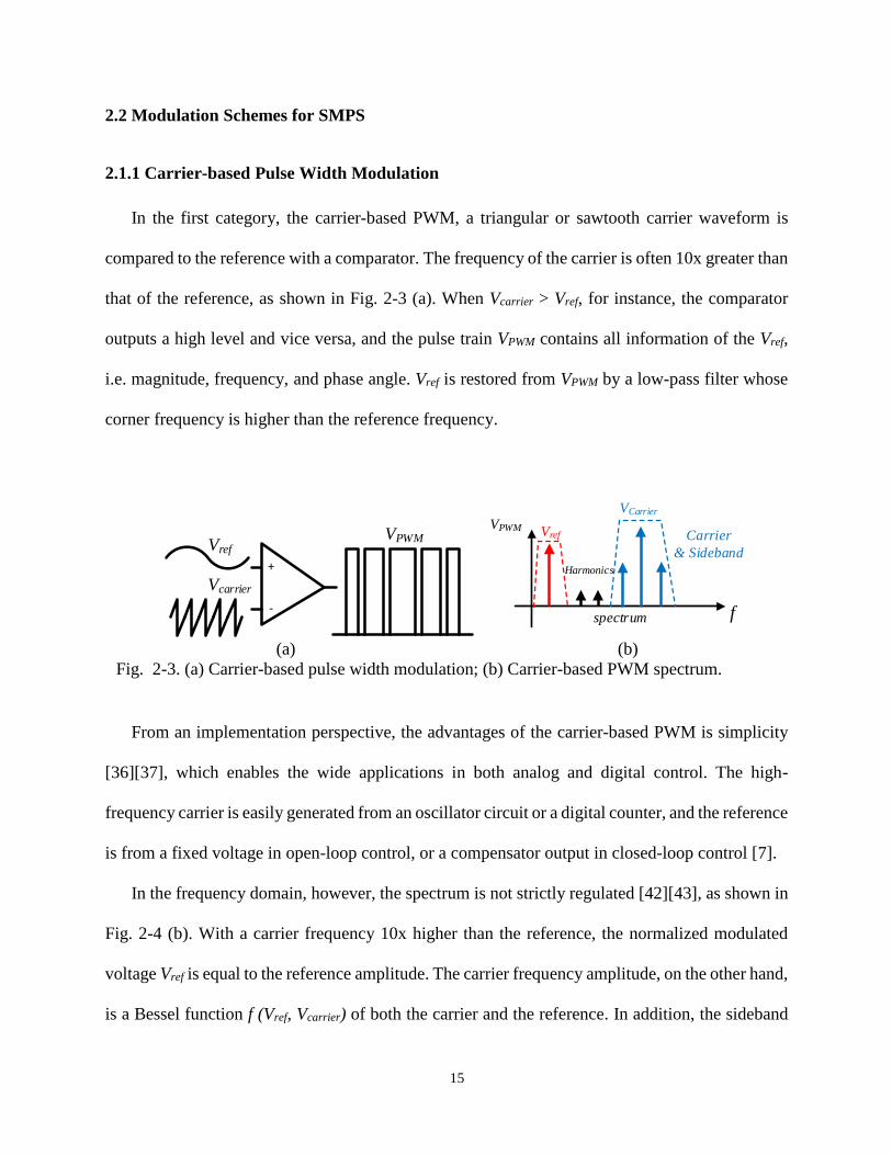
15
2.2 Modulation Schemes for SMPS
2.1.1 Carrier-based Pulse Width Modulation
In the first category, the carrier-based PWM, a triangular or sawtooth carrier waveform is
compared to the reference with a comparator. The frequency of the carrier is often 10x greater than
that of the reference, as shown in Fig. 2-3 (a). When Vcarrier > Vref, for instance, the comparator
outputs a high level and vice versa, and the pulse train VPWM contains all information of the Vref,
i.e. magnitude, frequency, and phase angle. Vref is restored from VPWM by a low-pass filter whose
corner frequency is higher than the reference frequency.
From an implementation perspective, the advantages of the carrier-based PWM is simplicity
[36][37], which enables the wide applications in both analog and digital control. The high-
frequency carrier is easily generated from an oscillator circuit or a digital counter, and the reference
is from a fixed voltage in open-loop control, or a compensator output in closed-loop control [7].
In the frequency domain, however, the spectrum is not strictly regulated [42][43], as shown in
Fig. 2-4 (b). With a carrier frequency 10x higher than the reference, the normalized modulated
voltage Vref is equal to the reference amplitude. The carrier frequency amplitude, on the other hand,
is a Bessel function f (Vref, Vcarrier) of both the carrier and the reference. In addition, the sideband
+
-
Vref
Vcarrier
VPWM
f
VPWM
spectrum
Carrier
& Sideband
Vref
VCarrier
Harmonics
(a) (b)
Fig. 2-3. (a) Carrier-based pulse width modulation; (b) Carrier-based PWM spectrum.
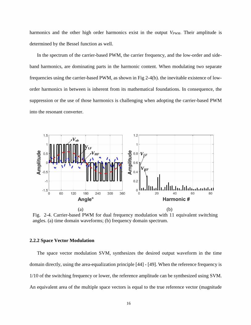
16
harmonics and the other high order harmonics exist in the output VPWM. Their amplitude is
determined by the Bessel function as well.
In the spectrum of the carrier-based PWM, the carrier frequency, and the low-order and side-
band harmonics, are dominating parts in the harmonic content. When modulating two separate
frequencies using the carrier-based PWM, as shown in Fig 2-4(b). the inevitable existence of low-
order harmonics in between is inherent from its mathematical foundations. In consequence, the
suppression or the use of those harmonics is challenging when adopting the carrier-based PWM
into the resonant converter.
2.2.2 Space Vector Modulation
The space vector modulation SVM, synthesizes the desired output waveform in the time
domain directly, using the area-equalization principle [44] - [49]. When the reference frequency is
1/10 of the switching frequency or lower, the reference amplitude can be synthesized using SVM.
An equivalent area of the multiple space vectors is equal to the true reference vector (magnitude
Vab
VLF
VHF VLF
VHF
(a) (b)
Fig. 2-4. Carrier-based PWM for dual frequency modulation with 11 equivalent switching
angles. (a) time domain waveforms; (b) frequency domain spectrum.
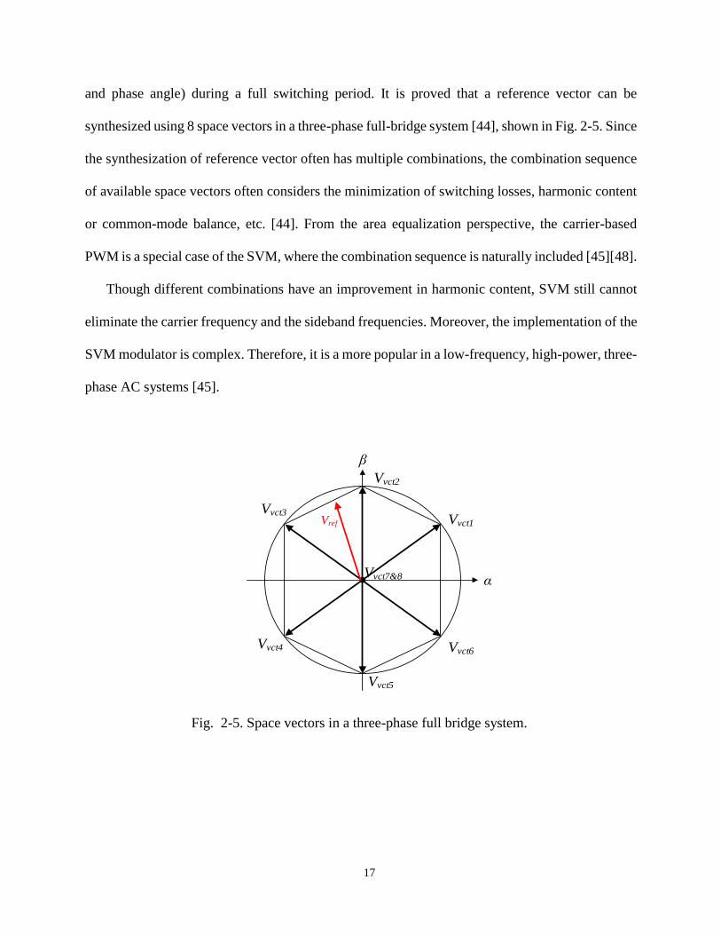
17
and phase angle) during a full switching period. It is proved that a reference vector can be
synthesized using 8 space vectors in a three-phase full-bridge system [44], shown in Fig. 2-5. Since
the synthesization of reference vector often has multiple combinations, the combination sequence
of available space vectors often considers the minimization of switching losses, harmonic content
or common-mode balance, etc. [44]. From the area equalization perspective, the carrier-based
PWM is a special case of the SVM, where the combination sequence is naturally included [45][48].
Though different combinations have an improvement in harmonic content, SVM still cannot
eliminate the carrier frequency and the sideband frequencies. Moreover, the implementation of the
SVM modulator is complex. Therefore, it is a more popular in a low-frequency, high-power, three-
phase AC systems [45].
β
α
Vvct1
Vvct2
Vvct3
Vvct4
Vvct5
Vvct6
Vvct7&8
Vref
Fig. 2-5. Space vectors in a three-phase full bridge system.
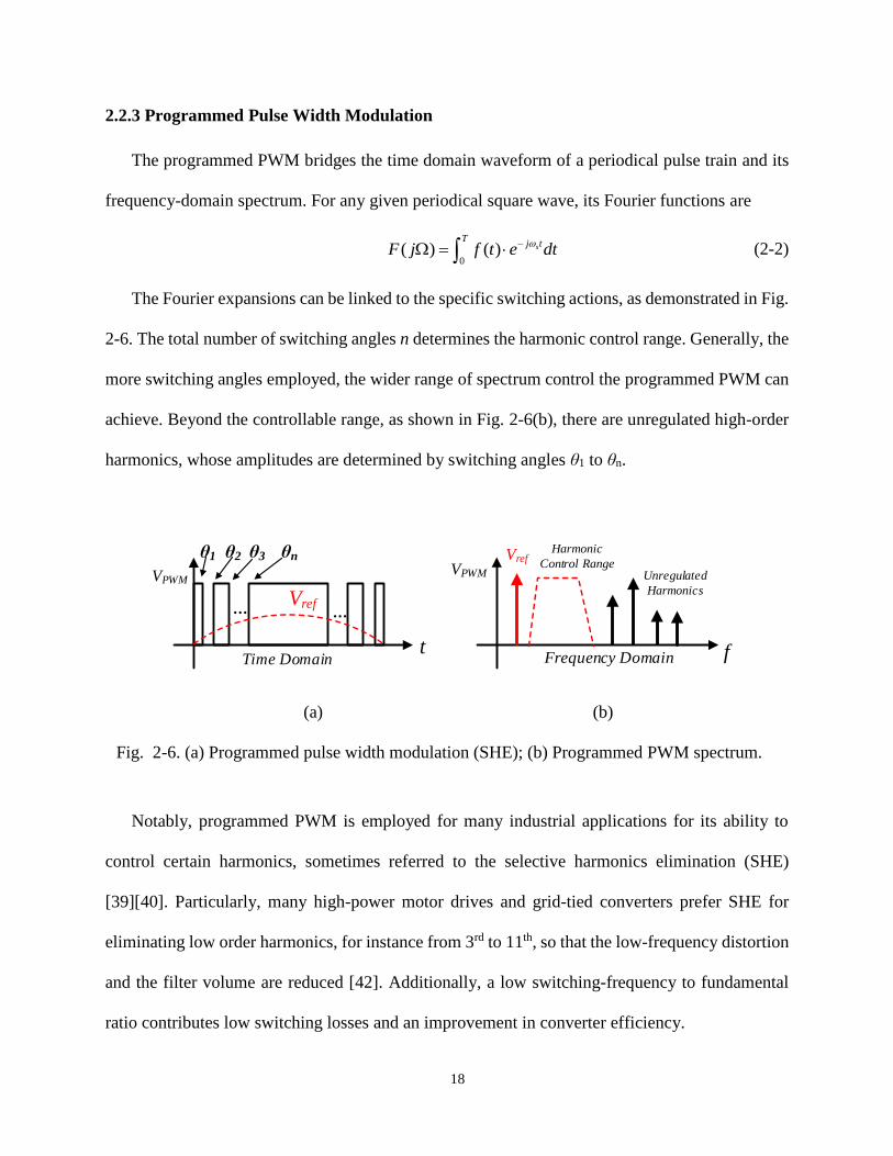
18
2.2.3 Programmed Pulse Width Modulation
The programmed PWM bridges the time domain waveform of a periodical pulse train and its
frequency-domain spectrum. For any given periodical square wave, its Fourier functions are
0
( ) ( ) sT
j tF j f t e dt
(2-2)
The Fourier expansions can be linked to the specific switching actions, as demonstrated in Fig.
2-6. The total number of switching angles n determines the harmonic control range. Generally, the
more switching angles employed, the wider range of spectrum control the programmed PWM can
achieve. Beyond the controllable range, as shown in Fig. 2-6(b), there are unregulated high-order
harmonics, whose amplitudes are determined by switching angles θ1 to θn.
Notably, programmed PWM is employed for many industrial applications for its ability to
control certain harmonics, sometimes referred to the selective harmonics elimination (SHE)
[39][40]. Particularly, many high-power motor drives and grid-tied converters prefer SHE for
eliminating low order harmonics, for instance from 3rd to 11th, so that the low-frequency distortion
and the filter volume are reduced [42]. Additionally, a low switching-frequency to fundamental
ratio contributes low switching losses and an improvement in converter efficiency.
θ1 θ2 θ3 θn
... ...
t
Vref
VPWM
Time Domain
fFrequency Domain
Unregulated
Harmonics
VrefHarmonic
Control RangeVPWM
(a) (b)
Fig. 2-6. (a) Programmed pulse width modulation (SHE); (b) Programmed PWM spectrum.
19
The drawbacks of programmed PWM are the excessive computation burden and
implementation difficulties. The Fourier expansion of the periodical pulse trains are a set of
transcendental equations involving trigonometry. It is difficult to derive all analytical solutions,
and thus numeric solutions using iteration methods, high-order polynomial equations, or non-linear
methods such as genetic algorithms are some popular approaches [78][80]. In addition, all pre-
determined switching patterns are required to programmed into controllers to avoid real-time
computation, and large memories to store all switching patterns as a look-up-table (LUT) are
employed. As a result, the real-time control for programmed PWM is challenging for high
frequency and time-constrained applications.
The programmed PWM is advantageous on the low-order harmonic suppression, which is
beneficial for the harmonic reduction in the resonant converter. Additionally, the programmed
PWM has the potential to modulate and control multiple frequencies in a wide range. In this
dissertation, programmed PWM is selected as a fundamental approach to investigate the multi-
frequency modulation and control for resonant converters.
2.3 Modulation and Control of Resonant Converter
In many resonant converters, the switching network generates a 50% duty cycle square
waveform whose frequency is the resonant frequency of the tank, as shown in Fig. 2-1. To regulate
the output power, some popular control strategies, e.g. the frequency modulation, the pulse density
modulation, and the duty cycle modulation, are developed for resonant converters [7][50-52],
given in Fig. 2-7.
These modulation schemes are used for precise output power regulation, rather than regulation
of harmonic content. Duty cycle modulation, for example, increases harmonic content, as the
magnitudes of the low-order harmonics rise when D ≠ 50%. There is no modulation scheme that
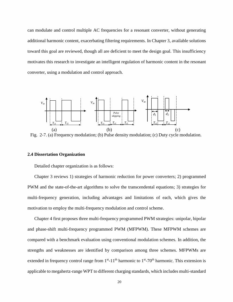
20
can modulate and control multiple AC frequencies for a resonant converter, without generating
additional harmonic content, exacerbating filtering requirements. In Chapter 3, available solutions
toward this goal are reviewed, though all are deficient to meet the design goal. This insufficiency
motivates this research to investigate an intelligent regulation of harmonic content in the resonant
converter, using a modulation and control approach.
2.4 Dissertation Organization
Detailed chapter organization is as follows:
Chapter 3 reviews 1) strategies of harmonic reduction for power converters; 2) programmed
PWM and the state-of-the-art algorithms to solve the transcendental equations; 3) strategies for
multi-frequency generation, including advantages and limitations of each, which gives the
motivation to employ the multi-frequency modulation and control scheme.
Chapter 4 first proposes three multi-frequency programmed PWM strategies: unipolar, bipolar
and phase-shift multi-frequency programmed PWM (MFPWM). These MFPWM schemes are
compared with a benchmark evaluation using conventional modulation schemes. In addition, the
strengths and weaknesses are identified by comparison among three schemes. MFPWMs are
extended in frequency control range from 1st-11th harmonic to 1st-70th harmonic. This extension is
applicable to megahertz-range WPT to different charging standards, which includes multi-standard
Vsn
Ts1 Ts2
Vsn
Ts1 Ts1 Ts1
Pulse
skipping
Vsn
Ts1 Ts1
d1 d2
(a) (b) (c)
Fig. 2-7. (a) Frequency modulation; (b) Pulse density modulation; (c) Duty cycle modulation.
21
wide-band MFPWM, and single-standard narrow-band MFPWM. Finally, MFPWM expands from
two-level converters to multilevel converters. A full mathematical description regarding multi-
frequency modulation is illustrated, and the solver, algorithms and full solution of this
transcendental problem are investigated.
Chapter 5 demonstrates two applications of resonant converters using the proposed multi-
frequency modulation and control scheme. Three MFPWM strategies enable an ultrasonic (US)
and radio-frequency (RF) combined electrosurgical power supply for a multi-functional surgical
device. The hazardous 100 kHz leakage currents are eliminated from the modulation, ensuring
patient safety. In addition, a dual-mode wireless power transfer transmitter is demonstrated using
MFPWM schemes, and a comparable efficiency and reduced hardware count are achieved with a
15 W prototype.
Chapter 6 investigates a new WPT architecture for 20 W fast charging applications, featuring
a multilevel switched capacitor (MSC) converter with reduced harmonic content and conduction
loss. First, several candidate topologies are evaluated using the same design parameters. The
operation principles of each candidate are illustrated, and their performances are quantized. Four
metrics in the topology evaluation, the regulation ability, efficiency, current THD and power
density, are considered among the four topologies. The proposed MSC rectifier is investigated
over different operation points. Two modulation and control strategies (stack and queue charge
control) are studied. Moreover, an impedance transformation theory for the WPT rectifier is
developed, which reveals the reasons for system efficiency improvement. An accurate loss model
of a 20 W prototype is analyzed and verified with the experimental results.
Chapter 7 elaborates the design and implementation of the proposed MSC rectifier for wireless
fast charging. A detailed device size procedure of the MSC rectifier is illustrated using IC process

22
parameters. The results confirm that the MSC rectifier is advantageous compared with the
conventional switched-capacitor step-down converter, using IC process parameters for on-chip
implementation. In addition, a closed-loop control is designed for the MSC rectifier, which
facilitates the output regulation and optimal efficiency tracking in WPT system. Finally, the
experimental results of efficiency tests, THD tests and closed-loop control test are shown to verify
the loss modeling, current THD modeling and closed-loop control of the MSC rectifier prototype.
Chapter 8 summarizes this dissertation and presents some potential future work.

23
3. Literature Review
From the discussion of two representative applications in Chapter 1 and Chapter 2, the
modulation and control of the harmonic content in resonant converters are important to limit
leakage harmonics for safety, or to enable combined functionality using simple hardware. This
chapter reviews state-of-the -art technologies to reveal motivations and challenges of this
dissertation.
Harmonic content is inherent in switched-mode power supplies, including dc/ac and ac/dc
resonant converters. State-of-the-art approaches of harmonic reduction, hardware-based and
modulation-based methods, are briefly reviewed. Techniques are not solely restricted to targeted
dc/ac and ac/dc resonant converters. Prior harmonic reduction approaches are not universally
suitable for the dc/ac and ac/dc resonant converter applications. Programmed PWM is identified
as a good candidate for harmonic reduction, and the research progresses in this field and the solving
algorithms are reviewed.
Another aspect of the research is revealing approaches to generate multiple ac frequencies from
a single resonant inverter. The multi-frequency generation, considering requirements for harmonic
reduction, creates a new opportunity and challenge for resonant converter control and modulation.
The state-of-the-art design of multi-frequency generators are reviewed.
3.1 Harmonic Content Reduction Approach
Harmonic content is inherent in switched mode power supplies due to the square wave
generation using semiconductor switches. The low-order harmonics in a square waveform result
in issues for many electrical systems. For power grids, the utility interface using power converters
require near sinusoidal, low-distortion currents at the line frequency (50/60 Hz). For
electrosurgical applications, the leakage harmonic current at sub 100 kHz range is dangerous for

24
the patient, as those frequencies will stimulate the muscle and nerves in human, resulting in
constractions during surgery or patient discomfort. Similarly, many WPT standards specify the
allowable frequency bands, and leakage harmonics potentially interfere with the sensitive circuitry
in consumer electronics. In consequence, harmonic reduction is important for both applications.
Harmonics are often filtered a the output with bulky passive filters, which are challenging to
implement in space-sensitive applications like ESGs and WPT receivers for mobile devices. On
the other hand, the operating frequency is much higher than utility applications, and fewer
switching actions are expected to reduce switching loss. Therefore, programmed PWM is a
promising candidate to reduce harmonics content for dc/ac and ac/dc resonant converter
applications, without adding extra hardware.
In summary, the switching frequency fs in utility applications are higher than the output
frequency fo. Many approaches reviewed in this section are suitable for utility applications. In
resonant converters, however, the switching frequency fs is equal to or close to the output
frequency fo to reduce switching loss. Therefore, passive filters or modulation schemes that
requires less switching actions are preferred.
3.1.1 Hardware-based Approaches
The traditional approach to attenuate undesired harmonics is to use passive filters, and the
design of passive filters depends on the attenuation requirement and specific converter topology.
A simple LC filter is often employed for dc/ac inverters for utility applications and motor drives
[53]. To further increase the attenuation of harmonics, more complex filter configurations such as
LCL or higher order filters can be adopted. In general, the design of passive filters is highly
dependent on specific requirements, which differs case to case. No universal rule is given here.
The advantage of using passive filters is easy implementation. The disadvantage is its bulky size.
25
For some utility applications, an active filter is employed to filter low-order harmonics [54]-
[56]. Active filter can improve the power density of the power electronics system while achieving
good filtering results. In some cases, a hybrid configuration of passive filters and active filters is
proposed. The placement of the active filter is flexible on ac side or dc side, and the principle is to
inject or absorb certain harmonics using power converters [57]. The advantage of active filters is
usually smaller size and flexible control on harmonic content compared to purely passive
approaches. On the other hand, the use of active filters is suitable for utility applications since the
line frequency is very low (50 Hz or 60 Hz), and state-of-the-art controllers can meet the bandwidth
requirements. For resonant converters where the “line frequency” is over one hundred kilohertz,
or even in the megahertz range, it is difficult, expensive or impossible to meet the bandwidth
requirements in this frequency range.
In some utility applications, interleaving multiple ac/dc rectifier can mitigate the amplitude of
switching frequency ripple and its harmonics [59], which helps to reduce low-order harmonic
content. However, such methods are not applicable to dc/ac and ac/dc resonant converters.
3.1.2 Software-based Approach
In many utility applications, modulation-based approaches, sometimes called “active wave-
shaping” [57], are proposed for harmonic reduction. The main idea is to use semiconductor
switches, rather than diode rectifiers at the line frequency, operated at high frequency and using a
modulation scheme to reduce current distortion. This PWM rectification targets to generate pure
sinusoidal waveforms from dc/ac or ac/dc converters. With carrier-based, or space-vector PWM
schemes, the line-frequency current usually has a low distortion when the ratio between the carrier
frequency and the line frequency is high. However, this leads to control complexity and high

26
switching losses when applying to the resonant converter applications, where the fundamental
frequency is over one hundred kilohertz.
Spread-spectrum techniques are used to alleviate acoustic noise [58] or conducted EMI [59]
when employing carrier-based PWM strategies. Those methods are effective to spread the special
content of the switching into a wider range, but the cost is increased computation burden. In general,
the carrier-based PWM for harmonic reduction is beneficial for line frequency applications. When
the modulation ratio is low, and the fundamental frequency is over one hundred kilohertz, or even
the megahertz range, the state-of-the-art controller cannot support enough computation ability and
the switching loss could be prohibitive.
3.2 Programmed PWM
For applications that require less switching actions, the programmed PWM is a good candidate.
Programmed PWM are conventionally used in utility interface power converters and megawatt
level motor drives. A detailed review for programmed PWM is provided as follows.
3.2.1 Programmed PWM Problem Formation
Programmed PWM, including selective harmonic elimination (SHE)-PWM, has been studied
for use in many industrial applications to reduce harmonic content, generated from a voltage-
source converter (VSC). Historically, programmed PWM was first investigated when the power
electronics technology emerged, as early as the 1960s [40], where this modulation scheme was
applied to a two-level or a three-level full-bridge converter.
Programmed PWM was later applied for multilevel converters, such as the diode-clamped, the
flying-capacitor, or the cascaded H-bridge converters [40][60-64]. Nowadays, this technique is
also applicable to many recent proposed modular multilevel converters (MMC). By integrating

27
programmed PWM schemes with different converter topologies, a distinct output THD and
efficiency can be achieved.
For a full-bridge converter with 2-level or 3-level output, two basic programmed PWM
waveforms, namely unipolar and bipolar waveforms, are often used, as demonstrated in Fig. 3-1.
The unipolar waveform, shown in Fig 3-1 (a) can reach positive, negative DC rail and a zero state.
The bipolar waveform has no zero states [63].
The waveforms in Fig. 3-1 can be divided into 1) quarter-wave symmetry, 2) half-wave
symmetry, and 3) non-symmetry [66]. The Fourier expansions of a quarter-wave symmetric
waveform will be simplified where all even-harmonics will be zero due to the waveform symmetry.
Assuming m switching angles per quarter wave, then the magnitude of the 1st, the 3rd to the (2m-
1) th frequencies are controlled to defined amplitudes.
For a half-wave symmetry waveform, all even harmonics are inherently zero as well due to
symmetry, however, computation burdens will be double since total 2m switching angles need to
be calculated per half wave to control from the 1st to the (2m-1) th harmonics. According to [66][67],
a total of 2m switching angles are required to control not only amplitude but also each harmonic
θ1θ2 θ3 θm...
π/2 π 3π/2
Vdc
-Vdc
θ1
θ2
θ3
θm
...
π/2 π 3π/2 2π
Vdc
-Vdc (a) (b)
Fig. 3-1. (a) Unipolar programmed PWM waveform; (b) Bipolar programmed PWM
waveform.
28
phase angle. Compared to the quarter-wave symmetric waveform, the half-wave symmetric
waveform can not only alter the amplitudes of each controlled frequency but also their phase angles.
For non-symmetric waveforms, switching angles for an entire switching period are calculated
to control amplitudes and phase angles of both even and odd harmonics, as well as dc bias. The
non-symmetric waveform offers the least constraints and most controllable variables. However,
the cost is more than quadruple computation burden compared with quarter-wave symmetry.
In this dissertation, the phase angles of each controlled frequency are not the focus. The
quarter-wave symmetric waveform is investigated for the MFPWM in Chapter 4, as the number
of the transcendental equations is minimal among the three categories, which presents least
computational burden to obtain the full sets of solutions.
3.2.2 Solving Algorithm
The mathematical format of the programmed PWM problem is a set of transcendental
equations, whose analytical solutions cannot be solved in generalized closed-form. Instead,
numerical methods to obtain the solutions of the transcendental equations problem are often
employed. In this section, some popular solving algorithms for the programmed PWM problems
are reviewed.
a) Gradient-based algorithm
The numerical iteration-based methodology, also one of the gradient-based algorithm, is first
employed to find accurate switching instances for the programmed PWM problem. The Newton-
Raphson numeric iteration method [37][38][68-72] is widely used for two-level and multilevel
programmed PWM problems. By providing an initial guess that is close to the true roots of the
transcendental equations, this algorithm searches for a set of solutions with minimal error by using
the gradient direction per iteration. The closer initial guess to the true solutions, the quicker this
29
algorithm executes. Consequently, using the Newton-Raphson method, the solution convergence
is dependent upon an initial guess being sufficiently close to the exact solution, which is
challenging when excessive switching angles are present.
Sun [70] discussed several approaches to select initial values such as linear function
approximation and incremental initial values. However, some prior knowledge (known as solution
points) is still required, and the assumption that trajectories of switching angles solutions are
continuous is made. This might not be true for multi-level programmed PWM issues, and initial
values are difficult to predict if switching angles increase.
The equivalent-area principle is also applied in programmed PWM problems to find initial
guesses. In [71] [72], several ways to obtain initial values based on equivalent area concepts are
discussed. This method is effective for arbitrary waveforms with few switching angles, however,
it can become complex and impractical when the number of switching instances increases.
In [73], transcendental equations are transformed into a set of Chebyshev functions, where the
Newton-Raphson iterations are employed to solve Chebyshev functions instead of trigonometric
functions. The convergence and computation time are improved in several case studies, but
effectiveness for large numbers of switching angles are is not examined.
b) Transcendental equation conversion-based algorithm
Direct numeric iterations of transcendental equations can be time-consuming, and thus
literature proposed methods to convert the equations into other mathematical problems and then
solve them. For example, in [74], Walsh functions are employed to convert trigonometric functions
into linear algebraic equations. When transcendental equations transform to linear algebraic
equations or high-order polynomial equations, there is no need to find out the initial values for the
30
numerical iteration methods. Instead, roots of linear algebraic equations or high-order polynomial
equations can be found without initial values..
As introduced in [75]-[79], programmed PWM problems are converted into polynomial
problems. Those polynomial equations can be solved directly with help of mathematical tools. Or,
in another approach, high-order polynomials use the Resultants Theory [75]-[77], or the Groebner
Theory [78] to first reduce order. Solving polynomial equations is straightforward, and the effort
of finding a good initial guess that is necessary for the Newton-Raphson method is reduced.
Another advantage of the conversion-based algorithm is that all possible solutions of the
transcendental equations can be found, and different solutions usually have varied output THDs
[79].
Nevertheless, the computation burden exponentially increases with a greater number of
switching angles. With large number of angles, high-performance computers are required to solve
the high-order polynomials, which is the key bottle-neck of the conversion-based algorithm.
Therefore, it is a useful tool only for programmed PWM problems with limited numbers of
switching angles. For instance, the number of switching angles in [75]-[78] is less than 15, using
a desktop computer.
c) Non-gradient based algorithm
Rather than treating the programmed PWM as a set of equations that need solutions, some non-
gradient based algorithms formulate this problem as a result-searching problem, where a gradient-
free algorithm is used to minimize a cost function related to the difference between the current and
desired harmonics [80]-[82]. The constraints of the final solution are identical to the numeric
iteration methods and the conversion-based algorithms. An initial estimation is still needed for the
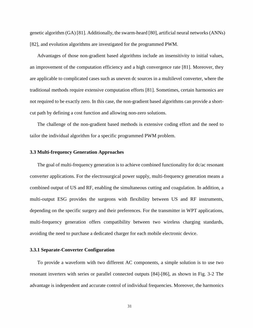
31
genetic algorithm (GA) [81]. Additionally, the swarm-heard [80], artificial neural networks (ANNs)
[82], and evolution algorithms are investigated for the programmed PWM.
Advantages of those non-gradient based algorithms include an insensitivity to initial values,
an improvement of the computation efficiency and a high convergence rate [81]. Moreover, they
are applicable to complicated cases such as uneven dc sources in a multilevel converter, where the
traditional methods require extensive computation efforts [81]. Sometimes, certain harmonics are
not required to be exactly zero. In this case, the non-gradient based algorithms can provide a short-
cut path by defining a cost function and allowing non-zero solutions.
The challenge of the non-gradient based methods is extensive coding effort and the need to
tailor the individual algorithm for a specific programmed PWM problem.
3.3 Multi-frequency Generation Approaches
The goal of multi-frequency generation is to achieve combined functionality for dc/ac resonant
converter applications. For the electrosurgical power supply, multi-frequency generation means a
combined output of US and RF, enabling the simultaneous cutting and coagulation. In addition, a
multi-output ESG provides the surgeons with flexibility between US and RF instruments,
depending on the specific surgery and their preferences. For the transmitter in WPT applications,
multi-frequency generation offers compatibility between two wireless charging standards,
avoiding the need to purchase a dedicated charger for each mobile electronic device.
3.3.1 Separate-Converter Configuration
To provide a waveform with two different AC components, a simple solution is to use two
resonant inverters with series or parallel connected outputs [84]-[86], as shown in Fig. 3-2 The
advantage is independent and accurate control of individual frequencies. Moreover, the harmonics
32
of the output frequencies can be suppressed if selective harmonic elimination is employed.
However, the dual-frequency, dual-inverter configuration fundamentally requires two sets of
independent inverters and filters, which increases the number of switching devices and passive
components, and overall cost, compared to a single-inverter counterpart.
The multi-frequency concept was raised in multi-receiver WPT applications as well [87]-[91].
In [87], each receiver is tuned to a separate frequency and the transmitter can feed only one receiver
at one time by varying its transmitting frequency. On the other hand, multiple power amplifiers,
tuned at different frequencies, are used to power individual loads simultaneously [89]. To improve
the power-sharing among multiple loads, several passive matching networks are also proposed to
enable selective power distribution [90]-[92]. None of these works addresses a transmitter that can
generate multiple frequencies simultaneously.
(a) (b)
Fig. 3-2. (a) Separate converter configuration for dual-frequency generations; (b)
Corresponding spectrum of separate converter configuration.
Q1 Q2
Q3 Q4
+
Vdc
-
+
Vab
-
a
b
Q5 Q6
Q7 Q8
+
Vdc
-
+
Vcd
-
c
d
LLF
CLF
LHF
CHF
* *
* *
LF Load
HF Load
VLF
VHF
fspectrum
VLFLF
Output
fspectrum
VHF
Harmonics
HF
Output
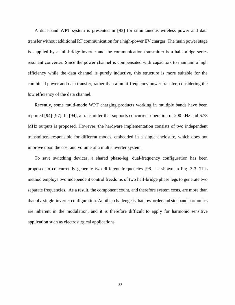
33
A dual-band WPT system is presented in [93] for simultaneous wireless power and data
transfer without additional RF communication for a high-power EV charger. The main power stage
is supplied by a full-bridge inverter and the communication transmitter is a half-bridge series
resonant converter. Since the power channel is compensated with capacitors to maintain a high
efficiency while the data channel is purely inductive, this structure is more suitable for the
combined power and data transfer, rather than a multi-frequency power transfer, considering the
low efficiency of the data channel.
Recently, some multi-mode WPT charging products working in multiple bands have been
reported [94]-[97]. In [94], a transmitter that supports concurrent operation of 200 kHz and 6.78
MHz outputs is proposed. However, the hardware implementation consists of two independent
transmitters responsible for different modes, embedded in a single enclosure, which does not
improve upon the cost and volume of a multi-inverter system.
To save switching devices, a shared phase-leg, dual-frequency configuration has been
proposed to concurrently generate two different frequencies [98], as shown in Fig. 3-3. This
method employs two independent control freedoms of two half-bridge phase legs to generate two
separate frequencies. As a result, the component count, and therefore system costs, are more than
that of a single-inverter configuration. Another challenge is that low-order and sideband harmonics
are inherent in the modulation, and it is therefore difficult to apply for harmonic sensitive
application such as electrosurgical applications.
34
(a)
(b)
Fig. 3-3. Shared phase-leg configuration for dual-frequency generation. (a) Schematic circuit;
(b) Spectrum.
Q1 Q2
Q3 Q4
+
Vdc
-
+
Vab
-
a
b
Q5
Q6
c+
Vbc
-
LLF
CLF
LHF
CHF
Shared phase-legLF phase-leg HF phase-leg
VLF
VHF
fspectrum
VLFLF
OutputHarmonics
fspectrum
VHF
Harmonics
HF
Output
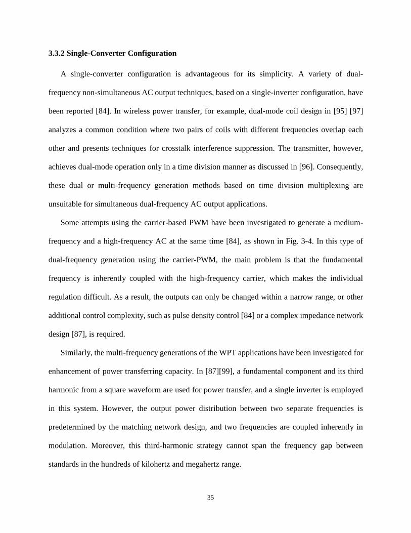
35
3.3.2 Single-Converter Configuration
A single-converter configuration is advantageous for its simplicity. A variety of dual-
frequency non-simultaneous AC output techniques, based on a single-inverter configuration, have
been reported [84]. In wireless power transfer, for example, dual-mode coil design in [95] [97]
analyzes a common condition where two pairs of coils with different frequencies overlap each
other and presents techniques for crosstalk interference suppression. The transmitter, however,
achieves dual-mode operation only in a time division manner as discussed in [96]. Consequently,
these dual or multi-frequency generation methods based on time division multiplexing are
unsuitable for simultaneous dual-frequency AC output applications.
Some attempts using the carrier-based PWM have been investigated to generate a medium-
frequency and a high-frequency AC at the same time [84], as shown in Fig. 3-4. In this type of
dual-frequency generation using the carrier-PWM, the main problem is that the fundamental
frequency is inherently coupled with the high-frequency carrier, which makes the individual
regulation difficult. As a result, the outputs can only be changed within a narrow range, or other
additional control complexity, such as pulse density control [84] or a complex impedance network
design [87], is required.
Similarly, the multi-frequency generations of the WPT applications have been investigated for
enhancement of power transferring capacity. In [87][99], a fundamental component and its third
harmonic from a square waveform are used for power transfer, and a single inverter is employed
in this system. However, the output power distribution between two separate frequencies is
predetermined by the matching network design, and two frequencies are coupled inherently in
modulation. Moreover, this third-harmonic strategy cannot span the frequency gap between
standards in the hundreds of kilohertz and megahertz range.
36
(a)
(b)
Fig. 3-4. Carrier-based PWM scheme for dual-frequency generation; (a) Schematic circuit; (b)
Spectrum.
Q1 Q2
Q3 Q4
+
Vdc
-
+
Vab
-
a
b
L1 C1
* *
L2
C2
f
Vab
spectrum
...
Carrier
& Sideband
VLF
VHF
37
A multilevel dual-frequency inverter is first proposed in [100] with some examples. In this
dissertation, a full problem formulation is provided in extend the concept of MFPWM in both full-
bridge and multilevel converters.
3.4 Challenge and Motivation
This chapter reviews the state-of-the-art approaches that utilize or suppress of harmonic
content for combined functionality with a simple structure or to limit leakage harmonics with
minimal components. For resonant converters that operate in the kilohertz or megahertz range,
using passive filters and programmed PWM are two practical approaches to reduce harmonic
content. To limit undesired harmonic content, bulky passive filters are common in conventional
ESGs and WPT systems but are challenging for space-sensitive applications.
The modulation and control of multiple frequencies offers flexibility for implementation with
a reduced size of passive filters. Particularly, by using a programmed multi-frequency PWM, a
range of frequencies in the output spectrum can be predicted and determined. This alleviates effort
in passive filter design because certain undesired harmonics are excluded from generation.
For multi-frequency generation, traditional single-frequency-generation strategies cannot meet
all needs of resonant converter applications, considering harmonic reduction. A new modulation
that is capable of controlling multiple frequencies using a single converter simplifies the converter
design, enables advanced performance, and reduces component count and cost.
38
4. Multi-Frequency Programmed Pulse Width Modulation
The state-of-the-art solutions presented in Chapter 3 cannot meet all the requirements for the
targeted applications. The passive filter is sometimes bulky to fit into space-sensitive applications,
such as WPT receiver on mobile devices. The carrier-based modulation schemes can generate
multiple frequencies using less semiconductor devices, but the low-order harmonic contents are
difficult to filter. The conventional programmed PWM has a good suppression on harmonic
content but can only generate one frequency, and multiple generators are needed for multi-output
applications.
This chapter proposes modulation schemes that enable multi-frequency generation and
independent output regulation using a single converter. The fundamental and certain harmonics
are independently controlled, allowing individual power regulation of multiple outputs. Also,
undesired harmonics in between output frequencies are easily eliminated from generation, which
prevents potential hazards. Finally, the proposed modulation schemes are applicable to a variety
of DC/AC topologies. Reduction of harmonic content and multi-frequency generation, are
combined using the proposed MFPWM scheme, achieving good balance on low harmonic content
and low component count.
A benchmark evaluation of the carrier-based PWM and programmed PWM is provided first.
Three MFPWM schemes (unipolar, bipolar and phase-shift MFPWM) are discussed based on a
two-level full-bridge converter. To address practical needs for an extensive frequency control
range (~70 harmonics), a study of extended-switching-angle MFPWM is presented. This extensive
MFPWM can control harmonics almost 5x than the traditional programmed PWM (<15 harmonics)
in past applications [21-28], which is beyond conventional solver space. Finally, MFPWM is
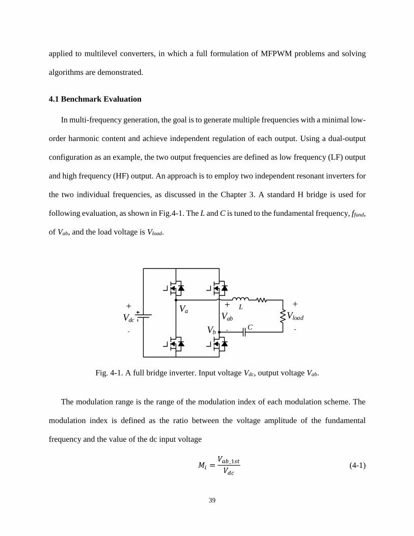
39
applied to multilevel converters, in which a full formulation of MFPWM problems and solving
algorithms are demonstrated.
4.1 Benchmark Evaluation
In multi-frequency generation, the goal is to generate multiple frequencies with a minimal low-
order harmonic content and achieve independent regulation of each output. Using a dual-output
configuration as an example, the two output frequencies are defined as low frequency (LF) output
and high frequency (HF) output. An approach is to employ two independent resonant inverters for
the two individual frequencies, as discussed in the Chapter 3. A standard H bridge is used for
following evaluation, as shown in Fig.4-1. The L and C is tuned to the fundamental frequency, ffund,
of Vab, and the load voltage is Vload.
The modulation range is the range of the modulation index of each modulation scheme. The
modulation index is defined as the ratio between the voltage amplitude of the fundamental
frequency and the value of the dc input voltage
𝑀𝑖 =𝑉𝑎𝑏_1𝑠𝑡
𝑉𝑑𝑐 (4-1)
+
Vdc
-
+
Vab
-
L
C
+
Vload
-
Va
Vb
Fig. 4-1. A full bridge inverter. Input voltage Vdc, output voltage Vab.

40
To simplify following analysis, Vdc = 1 is assumed and the output voltages, VLF and VHF, are
equal to their individual modulation indices.
𝑀𝑖 =𝑉𝑖
𝑉𝑑𝑐= 𝑉𝑖 (4-2)
The power delivered to the load is fixed when different modulation schemes are used.
Therefore, the conduction loss on the semiconductor switches and the passive components are the
same in each case. The primary difference in power loss is the switching losses on the
semiconductor devices.
4.1.1 Duty Cycle Modulation
A square voltage is widely used for resonant converters for simple implementation. The
inverter output Vab is a variable duty ratio square waveform, and the frequency is tuned to the
resonant frequency. The time domain waveforms and their spectra at different duty ratio are shown
in Fig. 4-2. The amplitudes of the fundamental and the harmonics can be calculated using Fourier
series, and vary with the duty cycle. At 50% duty cycle, as shown in Fig. 4-2(a) and (b), the Fourier
expansion of Vab is
𝑉𝑎𝑏 =4
𝜋[sin(𝜔𝑡) +
1
3sin(3𝜔𝑡) +
1
5sin(5𝜔𝑡) + ⋯ +
1
𝑛sin(𝑛𝜔𝑡) + ⋯ ] (4-3)
The worst case of the low-order harmonics occurs at 50% duty cycle. This duty cycle also
results in the highest modulation index. To remove the significant low-order harmonics like the
3rd and the 5th, extra filtering components such as a shunt filter are required. For the duty cycle
modulation, the modulation range is from 0 to 4/π.
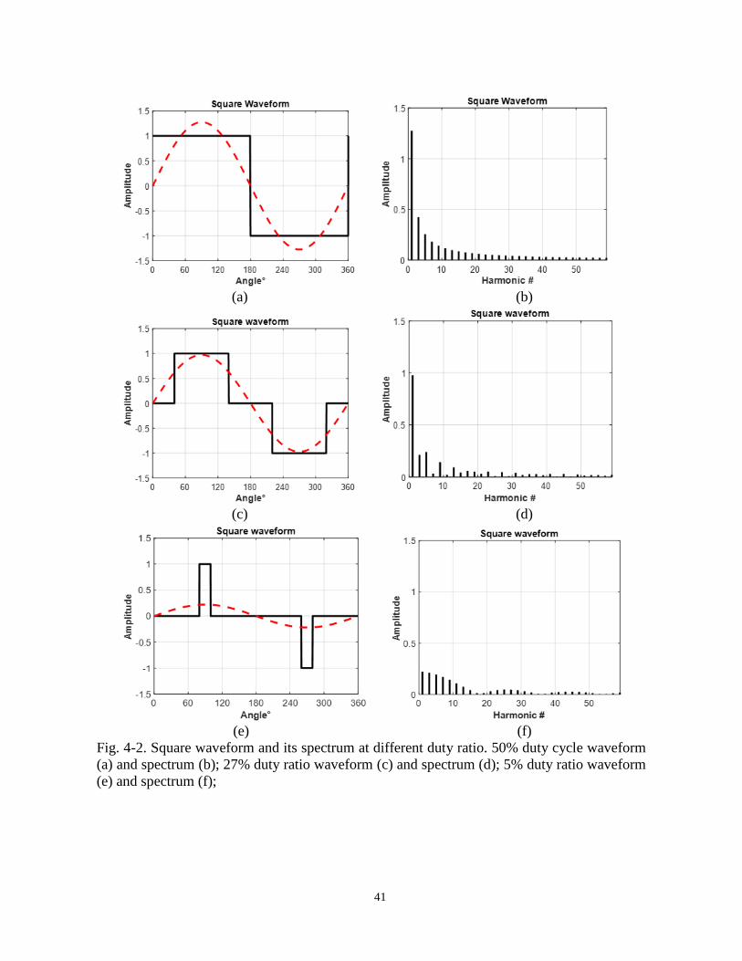
41
(a) (b)
(c) (d)
(e) (f)
Fig. 4-2. Square waveform and its spectrum at different duty ratio. 50% duty cycle waveform
(a) and spectrum (b); 27% duty ratio waveform (c) and spectrum (d); 5% duty ratio waveform
(e) and spectrum (f);

42
One advantage of using a square waveform is a favored condition at 50% duty cycle to achieve
soft switching transitions [7] where a low switching loss is realized. The switching losses include
the gate charge loss
𝑃𝑔𝑠 = 𝑄𝑔𝑠 ∙ 𝑉𝑔𝑠 ∙ 𝑓𝑓𝑢𝑛𝑑 (4-4)
and the output capacitance loss
𝑃𝑐𝑜𝑠𝑠 = 𝑄𝑜𝑠𝑠 ∙ 𝑉𝑑𝑐 ∙ 𝑓𝑓𝑢𝑛𝑑 (4-5)
To achieve LF and HF outputs, two H-bridge inverters are required. A summary of the square
wave modulation is shown in Table 4-1. In this case, the total switching loss is the sum of two
inverters
𝑃𝑠𝑞𝑢𝑎𝑟𝑒 = (4 ∙ 𝑄𝑔𝑠 ∙ 𝑉𝑔𝑠 + 4 ∙ 𝑄𝑜𝑠𝑠 ∙ 𝑉𝑑𝑐) ∙ 𝑓𝐿𝐹
+(4 ∙ 𝑄𝑔𝑠 ∙ 𝑉𝑔𝑠 + 4 ∙ 𝑄𝑜𝑠𝑠 ∙ 𝑉𝑑𝑐) ∙ 𝑓𝐻𝐹
(4-6)
4.1.2 Carrier-based PWM
Carrier-based PWM waveforms are shown in Fig. 4-3, where different modulation ratios are
demonstrated. The modulation ratio is the ratio between the carrier frequency to the fundamental
frequency.
𝑅𝑚𝑜𝑑 =𝑓𝑐𝑎𝑟𝑟𝑖𝑒𝑟
𝑓𝑓𝑢𝑛𝑑 (4-7)
As reviewed in previous chapters, one requirement of this modulation is that the carrier
frequency is significantly higher than the modulated waveform, often 10x or more. When the
modulation ratio is very low, for example 3 in Fig. 4-3 (a) and (b), the resultant fundamental
element in the spectrum is higher than the modulated value, which leads to a control error.
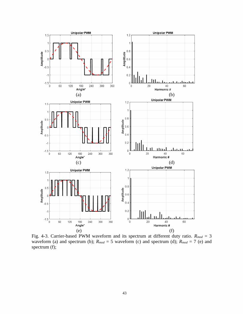
43
(a) (b)
(c) (d)
(e) (f)
Fig. 4-3. Carrier-based PWM waveform and its spectrum at different duty ratio. Rmod = 3
waveform (a) and spectrum (b); Rmod = 5 waveform (c) and spectrum (d); Rmod = 7 (e) and
spectrum (f);
44
Also, considerable low-order harmonics occur adjacent to the fundamental elements, which
require complex filter design to suppress them to zero. When the modulation ratio increases, the
carrier frequency is further from the fundamental frequency, and is easier to filter. The distribution
of the carrier frequency and their sidebands follows Bessel function of the modulation index and
the modulation ratio [37]. The modulation range of the carrier-based PWM is from 0 to 1.
For the carrier-based PWM, a larger number of switching actions is required, compared to the
square wave case, and all switching transitions are the hard switching. The switching loss
calculation is the same as the square wave case. To achieve two outputs, two inverters are
employed. For the unipolar PWM, one phase leg switches at the resonant frequency fs, and another
phase leg switches at the carrier frequency Rmod∙fs. The total switching loss of the carrier-based
PWM is
𝑃𝑐𝑎𝑟𝑟𝑖𝑒𝑟 = (2 ∙ 𝑄𝑔𝑠 ∙ 𝑉𝑔𝑠 + 2 ∙ 𝑄𝑜𝑠𝑠 ∙ 𝑉𝑑𝑐) ∙ (1 + 2𝑅𝑚𝑜𝑑 − 1) ∙ 𝑓𝐿𝐹
+(2 ∙ 𝑄𝑔𝑠 ∙ 𝑉𝑔𝑠 + 2 ∙ 𝑄𝑜𝑠𝑠 ∙ 𝑉𝑑𝑐) ∙ (1 + 2𝑅𝑚𝑜𝑑 − 1) ∙ 𝑓𝐻𝐹 (4-8)
4.1.3 SHE
SHE waveforms are shown in Fig. 4-4, where different switching angles per quarter wave are
demonstrated. For example, three switching angles θ1, θ2, and θ3 are pre-calculated in Fig. 4-4(a).
Since it is quarter-wave symmetric, there is a constraint 0< θ1 < θ2 < θ3 < π/2. The modulation
range is shown in Fig. 4-5(a). The x-axis is the modulation index of the fundamental frequency,
and the y-axis is the switching angles θ1, θ2, and θ3. The vertical red line indicates the maximum
modulation index with valid solutions.
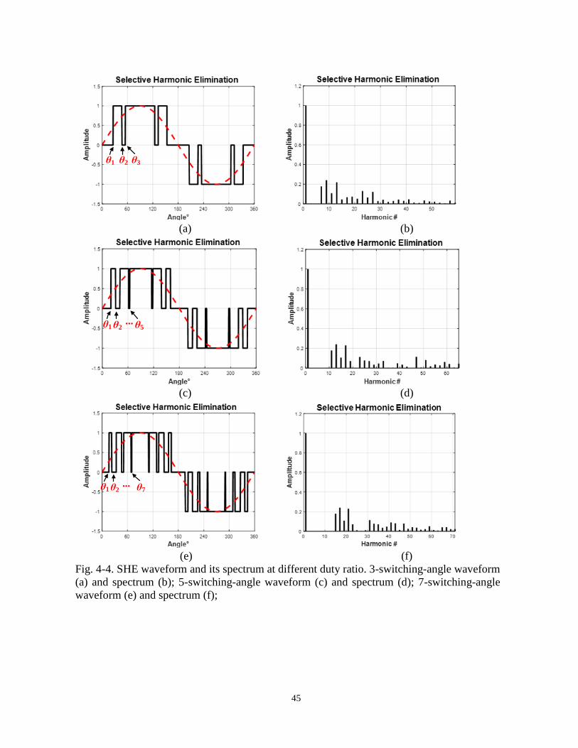
45
θ1 θ2 θ3
(a) (b)
θ1 θ2 θ5...
(c) (d)
θ1 θ2 θ7...
(e) (f)
Fig. 4-4. SHE waveform and its spectrum at different duty ratio. 3-switching-angle waveform
(a) and spectrum (b); 5-switching-angle waveform (c) and spectrum (d); 7-switching-angle
waveform (e) and spectrum (f);
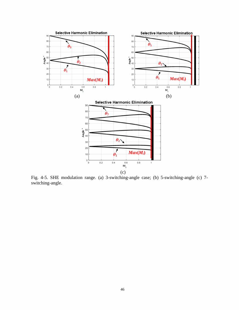
46
θ1
θ2
θ3
Max(Mi)
Max(Mi)θ1
θ2
θ5
(a) (b)
Max(Mi)θ1
θ2
θ7
(c)
Fig. 4-5. SHE modulation range. (a) 3-switching-angle case; (b) 5-switching-angle (c) 7-
switching-angle.

47
In general, SHE was developed to control a fundamental, often the line frequency, while
eliminating the low-order harmonics. The number of harmonics eliminated is limited by the
number of switching angles. For example, if the modulation consists of m switching angles per
quarter-wave, a finite number of harmonics of the fundamental n = f(m) can be controlled, where
n is a function of the number of switching angles and the modulation scheme (unipolar, bipolar,
multilevel, etc.). Harmonics higher than the nth are unregulated. Note that f(m) is a monotonic
function, indicating that more harmonics may be suppressed by increasing the number of switching
angles, m, which increases the equivalent switching frequency of the converter.
The actual switching frequency fs is defined as:
𝑓𝑠 = (2𝑚 − 1) ∙ 𝑓𝑓𝑢𝑛𝑑 (4-9)
where m is an odd integer greater than one.
For example, three switching angles per quarter-wave can control harmonics up to the 5th
harmonic as shown in Fig. 4-4 (a) and (b). The more switching angles used, the more harmonics
are controlled. The advantage of SHE modulation is that there is no need for extra filters for low-
order harmonics such as the 3rd and the 5th.
The modulation range of SHE is also dependent on the total number of switching angles per
quarter-wave, m, as shown in Fig. 4-5. For 3 switching angles per quarter-wave, the modulation
range is from 0 to 1.15. When m rises to seven, the modulation range is from 0 to 1. When m
increases to 39 per quarter-wave, the maximum modulation index is 0.99. As a result, the
modulation range of SHE is from 0 to 1 for single-frequency output. For the dual-output purpose,
two inverters are employed. The loss modeling of SHE is similar to the carrier-based PWM, where
most switching transitions are hard switching. The switching loss is
𝑃𝑆𝐻𝐸 = (2 ∙ 𝑄𝑔𝑠 ∙ 𝑉𝑔𝑠 + 2 ∙ 𝑄𝑜𝑠𝑠 ∙ 𝑉𝑑𝑐) ∙ (1 + 2𝑚 − 1) ∙ 𝑓𝐿𝐹
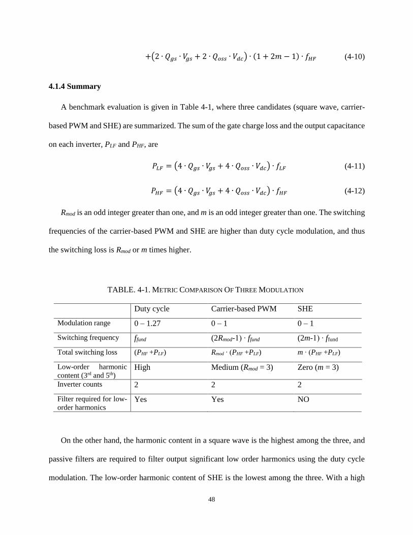
48
+(2 ∙ 𝑄𝑔𝑠 ∙ 𝑉𝑔𝑠 + 2 ∙ 𝑄𝑜𝑠𝑠 ∙ 𝑉𝑑𝑐) ∙ (1 + 2𝑚 − 1) ∙ 𝑓𝐻𝐹 (4-10)
4.1.4 Summary
A benchmark evaluation is given in Table 4-1, where three candidates (square wave, carrier-
based PWM and SHE) are summarized. The sum of the gate charge loss and the output capacitance
on each inverter, PLF and PHF, are
𝑃𝐿𝐹 = (4 ∙ 𝑄𝑔𝑠 ∙ 𝑉𝑔𝑠 + 4 ∙ 𝑄𝑜𝑠𝑠 ∙ 𝑉𝑑𝑐) ∙ 𝑓𝐿𝐹 (4-11)
𝑃𝐻𝐹 = (4 ∙ 𝑄𝑔𝑠 ∙ 𝑉𝑔𝑠 + 4 ∙ 𝑄𝑜𝑠𝑠 ∙ 𝑉𝑑𝑐) ∙ 𝑓𝐻𝐹 (4-12)
Rmod is an odd integer greater than one, and m is an odd integer greater than one. The switching
frequencies of the carrier-based PWM and SHE are higher than duty cycle modulation, and thus
the switching loss is Rmod or m times higher.
On the other hand, the harmonic content in a square wave is the highest among the three, and
passive filters are required to filter output significant low order harmonics using the duty cycle
modulation. The low-order harmonic content of SHE is the lowest among the three. With a high
TABLE. 4-1. METRIC COMPARISON OF THREE MODULATION
Duty cycle Carrier-based PWM SHE
Modulation range 0 – 1.27 0 – 1 0 – 1
Switching frequency ffund (2Rmod-1) ∙ ffund (2m-1) ∙ ffund
Total switching loss (PHF +PLF) Rmod ∙ (PHF +PLF) m ∙ (PHF +PLF)
Low-order harmonic
content (3rd and 5th) High Medium (Rmod = 3) Zero (m = 3)
Inverter counts 2 2 2
Filter required for low-
order harmonics Yes Yes NO
49
modulation ratio, the carrier frequency and its sidebands occur at frequencies much higher than
the fundamental, and thus low-order the harmonic content of the carrier-based PWM is inversely
related to the modulation ratio.
4.2 MFPWM Formulation: Unipolar, Bipolar and Phase-shift
All modulation schemes in Section 4.1 require two independent inverters for a dual-output
configuration. In addition, the duty cycle modulation and the carrier-based PWM require extra
filters to attenuate the adjacent low-order harmonics. To achieve combined functionality while
eliminating undesired low-order harmonics, multi-frequency programmed PWM is proposed.
Rather than generating a single fundamental frequency, MFPWM regulates the amplitude of
the fundamental and a specific kth harmonic to non-zero values, while canceling all harmonics in
between and, possibly, a number of harmonics above the kth. In this section, the MFPWM
formulation using a full bridge converter is investigated, and unipolar, bipolar and phase-shift
MFPWM schemes are studied.
4.2.1 Unipolar MFPWM
A standard full bridge DC/AC inverter is selected to demonstrate the proposed MFPWM
modulation methods [101]. The waveform of unipolar MFPWM is shown in Fig. 4-6. The
switching angles θ1, θ2, θ3 … θm of the quarter symmetric unipolar waveform are calculated using
the proposed MFPWM algorithms. The modulation indices MiLF and MiHF are defined by
normalizing the output voltages by the input dc bus voltage.
𝑀𝑖𝐿𝐹 =𝑉𝐿𝐹
𝑉𝑑𝑐 (4-13)
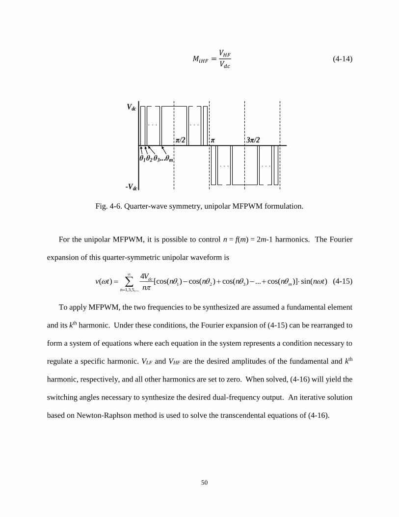
50
𝑀𝑖𝐻𝐹 =𝑉𝐻𝐹
𝑉𝑑𝑐 (4-14)
For the unipolar MFPWM, it is possible to control n = f(m) = 2m-1 harmonics. The Fourier
expansion of this quarter-symmetric unipolar waveform is
1 2 3
1,3,5,...
4( ) [cos( ) cos( ) cos( ) ... cos( )] sin( )dc
m
n
Vv t n n n n n t
n
(4-15)
To apply MFPWM, the two frequencies to be synthesized are assumed a fundamental element
and its kth harmonic. Under these conditions, the Fourier expansion of (4-15) can be rearranged to
form a system of equations where each equation in the system represents a condition necessary to
regulate a specific harmonic. VLF and VHF are the desired amplitudes of the fundamental and kth
harmonic, respectively, and all other harmonics are set to zero. When solved, (4-16) will yield the
switching angles necessary to synthesize the desired dual-frequency output. An iterative solution
based on Newton-Raphson method is used to solve the transcendental equations of (4-16).
θ1θ2 θ3 θm...
π/2 π 3π/2
Vdc
-Vdc
Fig. 4-6. Quarter-wave symmetry, unipolar MFPWM formulation.
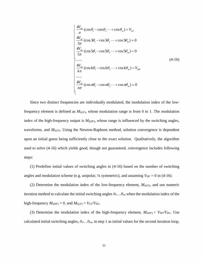
51
1 2
1 2
1 2
1 2
1 2
4(cos cos cos )
4(cos3 cos3 cos3 ) 0
3
4(cos5 cos5 cos5 ) 0
5
......
4(cos cos cos )
......
4(cos cos cos ) 0
dcm LF
dcm
dcm
dcm HF
dcm
VV
V
V
Vk k k V
k
Vn n n
n
(4-16)
Since two distinct frequencies are individually modulated, the modulation index of the low-
frequency element is defined as Mi(LF), whose modulation range is from 0 to 1. The modulation
index of the high-frequency output is Mi(HF), whose range is influenced by the switching angles,
waveforms, and Mi(LF). Using the Newton-Raphson method, solution convergence is dependent
upon an initial guess being sufficiently close to the exact solution. Qualitatively, the algorithm
used to solve (4-16) which yields good, though not guaranteed, convergence includes following
steps:
(1) Predefine initial values of switching angles in (4-16) based on the number of switching
angles and modulation scheme (e.g. unipolar, ¼ symmetric), and assuming VHF = 0 in (4-16).
(2) Determine the modulation index of the low-frequency element, Mi(LF), and use numeric
iteration method to calculate the initial switching angles θi1…θim when the modulation index of the
high-frequency Mi(HF) = 0, and Mi(LF) = VLF/VDC.
(3) Determine the modulation index of the high-frequency element, Mi(HF) = VHF/VDC. Use
calculated initial switching angles, θi1…θim, in step 1 as initial values for the second iteration loop,
52
and then perform numeric iteration to find the final switching angles, θ1…θm, of the desired
MFPWM waveforms.
A unipolar MFPWM example with 5 switching angles per quarter-wave is shown in Fig. 4-7.
The LF output is fixed at 0.6 and the modulation range of Mi(HF) is shown in Fig. 4-7(c), where no
solution exists above Mi(LF) = 0.6. In the time domain waveforms in Fig. 4-7 (a), the fundamental
frequency is used for LF output, and the 9th harmonic is used for HF output. In Fig. 4-7(b), the
spectrum of the single inverter output Vab is shown, where two frequencies are independently
generated using a single inverter, and there is zero low-order harmonic content adjacent to the LF
output.
4.1.2 Bipolar MFPWM
The Fourier expansion of the bipolar MFPWM waveforms, shown in Fig. 4-8, is
1 2 3
1,3,5,...
4( ) [1 2cos( ) 2cos( ) 2cos( ) ... 2cos( )] sin( )dc
m
n
Vv t n n n n n t
n
(4-17)
The transcendental equations for bipolar modulation are
1 2
1 2
1 2
1 2
1 2
4(1 2cos 2cos 2cos )
4(1 2cos3 2cos3 2cos3 ) 0
3
4(1 2cos5 2cos5 2cos5 ) 0
5
......
4(1 2cos 2cos 2cos )
......
4(1 2cos cos 2cos )
dcm LF
dcm
dcm
dcm HF
dcm
VV
V
V
Vk k k V
k
Vn n n
n
0
(4-18)
The previous algorithm for solving (4-16) is applicable to the bipolar case in (4-15).
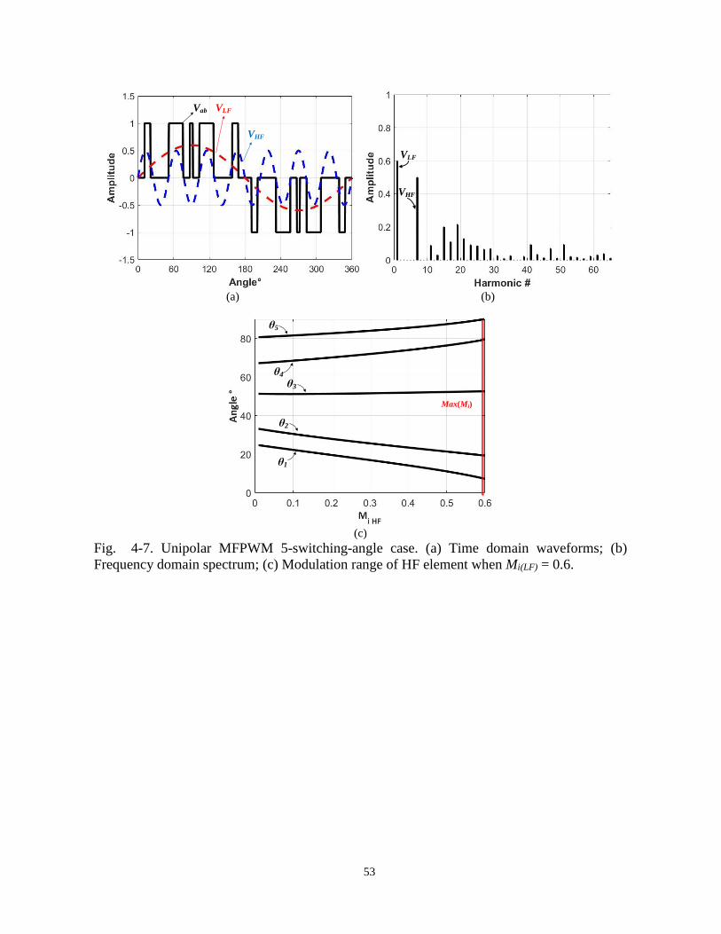
53
Vab VLF
VHF
VLF
VHF
(a) (b)
θ1
θ2
θ3
θ4
θ5
Max(Mi)
(c)
Fig. 4-7. Unipolar MFPWM 5-switching-angle case. (a) Time domain waveforms; (b)
Frequency domain spectrum; (c) Modulation range of HF element when Mi(LF) = 0.6.
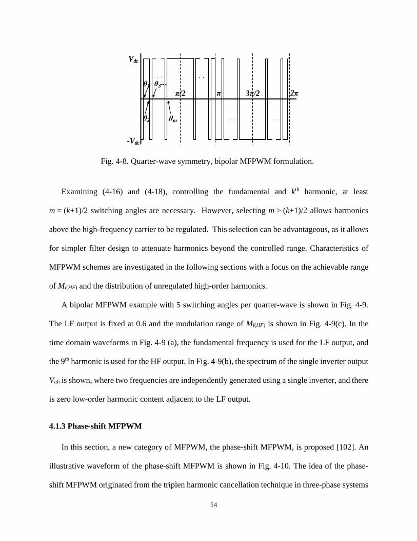
54
Examining (4-16) and (4-18), controlling the fundamental and kth harmonic, at least
m = (k+1)/2 switching angles are necessary. However, selecting m > (k+1)/2 allows harmonics
above the high-frequency carrier to be regulated. This selection can be advantageous, as it allows
for simpler filter design to attenuate harmonics beyond the controlled range. Characteristics of
MFPWM schemes are investigated in the following sections with a focus on the achievable range
of Mi(HF) and the distribution of unregulated high-order harmonics.
A bipolar MFPWM example with 5 switching angles per quarter-wave is shown in Fig. 4-9.
The LF output is fixed at 0.6 and the modulation range of Mi(HF) is shown in Fig. 4-9(c). In the
time domain waveforms in Fig. 4-9 (a), the fundamental frequency is used for the LF output, and
the 9th harmonic is used for the HF output. In Fig. 4-9(b), the spectrum of the single inverter output
Vab is shown, where two frequencies are independently generated using a single inverter, and there
is zero low-order harmonic content adjacent to the LF output.
4.1.3 Phase-shift MFPWM
In this section, a new category of MFPWM, the phase-shift MFPWM, is proposed [102]. An
illustrative waveform of the phase-shift MFPWM is shown in Fig. 4-10. The idea of the phase-
shift MFPWM originated from the triplen harmonic cancellation technique in three-phase systems
θ1
θ2
θ3
θm
...
π/2 π 3π/2 2π
Vdc
-Vdc
Fig. 4-8. Quarter-wave symmetry, bipolar MFPWM formulation.
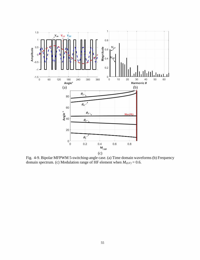
55
Vab VLF VHF
VLF
VHF
(a) (b)
θ1
θ2
θ3
θ4
θ5
Max(Mi)
(c)
Fig. 4-9. Bipolar MFPWM 5-switching-angle case. (a) Time domain waveforms (b) Frequency
domain spectrum. (c) Modulation range of HF element when Mi(LF) = 0.6.
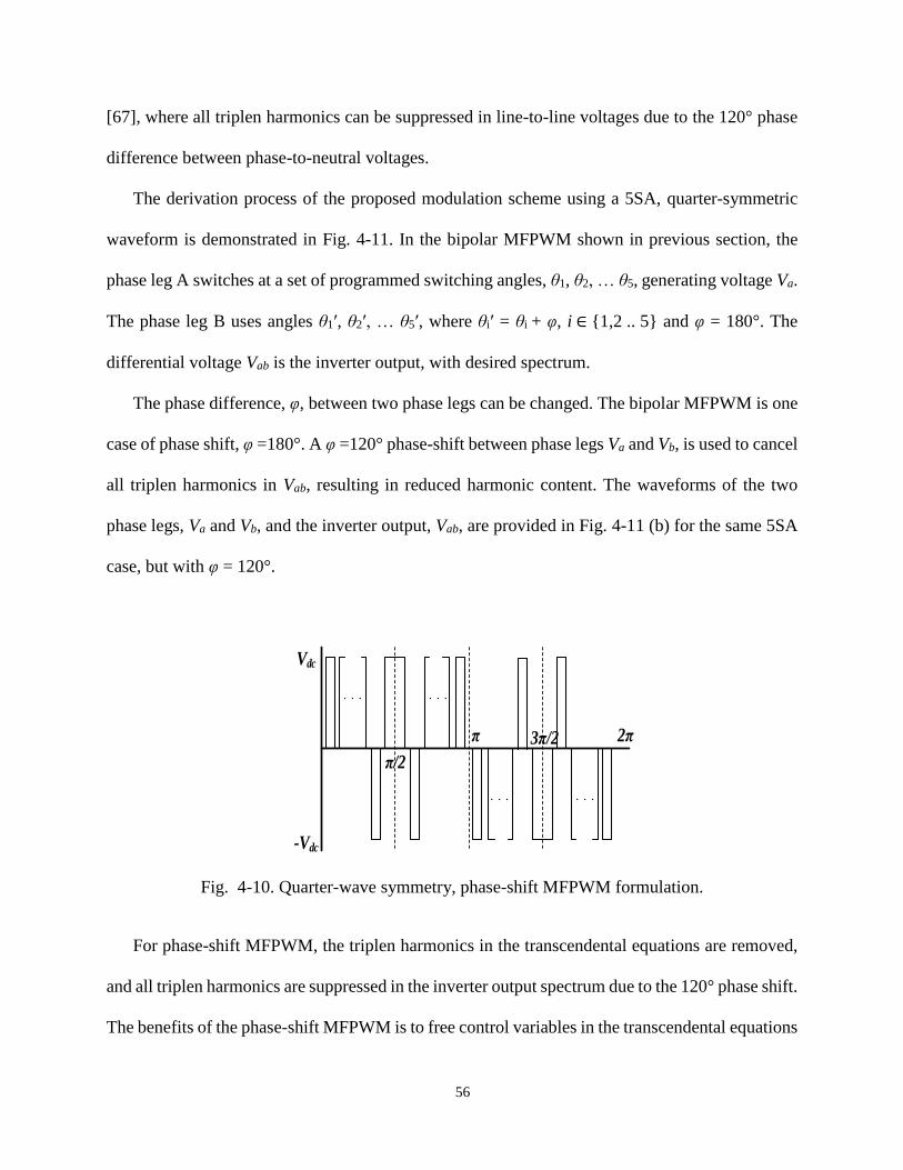
56
[67], where all triplen harmonics can be suppressed in line-to-line voltages due to the 120° phase
difference between phase-to-neutral voltages.
The derivation process of the proposed modulation scheme using a 5SA, quarter-symmetric
waveform is demonstrated in Fig. 4-11. In the bipolar MFPWM shown in previous section, the
phase leg A switches at a set of programmed switching angles, θ1, θ2, … θ5, generating voltage Va.
The phase leg B uses angles θ1ʹ, θ2ʹ, … θ5ʹ, where θiʹ = θi + φ, i ∈ 1,2 .. 5 and φ = 180°. The
differential voltage Vab is the inverter output, with desired spectrum.
The phase difference, φ, between two phase legs can be changed. The bipolar MFPWM is one
case of phase shift, φ =180°. A φ =120° phase-shift between phase legs Va and Vb, is used to cancel
all triplen harmonics in Vab, resulting in reduced harmonic content. The waveforms of the two
phase legs, Va and Vb, and the inverter output, Vab, are provided in Fig. 4-11 (b) for the same 5SA
case, but with φ = 120°.
For phase-shift MFPWM, the triplen harmonics in the transcendental equations are removed,
and all triplen harmonics are suppressed in the inverter output spectrum due to the 120° phase shift.
The benefits of the phase-shift MFPWM is to free control variables in the transcendental equations
π/2
π 3π/2 2π
Vdc
-Vdc
Fig. 4-10. Quarter-wave symmetry, phase-shift MFPWM formulation.
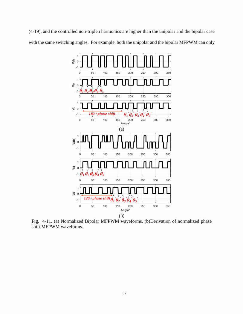
57
(4-19), and the controlled non-triplen harmonics are higher than the unipolar and the bipolar case
with the same switching angles. For example, both the unipolar and the bipolar MFPWM can only
θ1 θ2 θ3θ3 θ4 θ5
θ2ʹ θ3
ʹ θ4
ʹ θ5
ʹ
180 phase shift θ1ʹ
(a)
θ1 θ2 θ3θ3 θ4 θ5
120 phase shift θ2ʹ θ3
ʹ θ4
ʹ θ5
ʹ θ1
ʹ
(b)
Fig. 4-11. (a) Normalized Bipolar MFPWM waveforms. (b)Derivation of normalized phase
shift MFPWM waveforms.
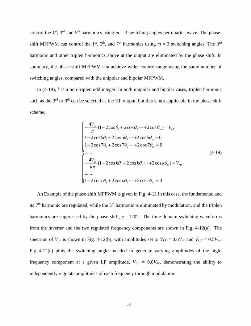
58
control the 1st, 3rd and 5th harmonics using m = 3 switching angles per quarter-wave. The phase-
shift MFPWM can control the 1st, 5th, and 7th harmonics using m = 3 switching angles. The 3rd
harmonic and other triplen harmonics above at the output are eliminated by the phase shift. In
summary, the phase-shift MFPWM can achieve wider control range using the same number of
switching angles, compared with the unipolar and bipolar MFPWM.
In (4-19), k is a non-triplen odd integer. In both unipolar and bipolar cases, triplen harmonic
such as the 3rd or 9th can be selected as the HF output, but this is not applicable in the phase shift
scheme,
1 2
1 2
1 2
1 2
1 2
4(1 2cos 2cos 2cos )
1 2cos5 2cos5 2cos5 0
1 2cos 7 2cos 7 2cos 7 0
......
4(1 2cos 2cos 2cos )
......
1 2cos 2cos 2cos 0
dcm LF
m
m
dcm HF
m
VV
Vk k k V
k
n n n
(4-19)
An Example of the phase-shift MFPWM is given in Fig. 4-12 In this case, the fundamental and
its 7th harmonic are regulated, while the 5th harmonic is eliminated by modulation, and the triplen
harmonics are suppressed by the phase shift, φ =120°. The time-domain switching waveforms
from the inverter and the two regulated frequency components are shown in Fig. 4-12(a). The
spectrum of Vab is shown in Fig. 4-12(b), with amplitudes set to VLF = 0.6Vdc and VHF = 0.5Vdc.
Fig. 4-12(c) plots the switching angles needed to generate varying amplitudes of the high-
frequency component at a given LF amplitude, VLF = 0.6Vdc, demonstrating the ability to
independently regulate amplitudes of each frequency through modulation.
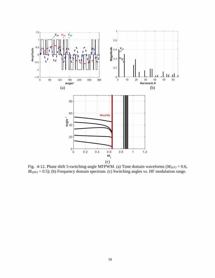
59
Vab VLF VHF
VLF
VHF
(a) (b)
Max(Mi)
(c)
Fig. 4-12. Phase shift 5-switching-angle MFPWM. (a) Time domain waveforms (Mi(LF) = 0.6,
Mi(HF) = 0.5); (b) Frequency domain spectrum. (c) Switching angles vs. HF modulation range.

60
Since there is a phase-shift between two phase legs, the amplitude of differential ac elements
in phase-shift MFPWM will be lower than the differential |Va-Vb| when φ =180°. The amplitude of
generated LF output is
(Mi)
3| | | 0.5 sin( ) 0.5 sin( ) |
2LF LF fund LF fund LFV V t V t V (4-20)
where the LF variables are the fundamental elements in two phase legs with 120° phase shift, and
the HF variables are the modulated kth harmonics in each phase leg, and HF output is
(Mi)
3| | | 0.5 sin( ) 0.5 sin( )
2HF HF k HF k HFV V t V t V (4-21)
4.3 MFPWM Evaluation
The evaluation of the proposed MFPWM has three aspects. 1) Modulation range. Since two
frequencies are modulated using MFPWM, the two modulation indices, MiLF and MiHF, have
limited range and the valid range is metrics to evaluate the flexibility of three MFPWMs. 2)
Switching loss. Using the loss model in the benchmark evaluation, the switching losses of three
MFPWM are estimated and compared. 3) Harmonic content. Three MFPWM schemes can
suppress certain low-order harmonics, but with different THD. The worst cases of the three
MFPWMs and a simplified analysis are given to quantify the differences.
4.3.1 Modulation range
In the benchmark evaluation of SHE in Fig. 4-4, the range of the modulation index Mi decreases
from 1.15 to 0.99 when m increases from 3 to 39. The number of the switching angles impacts the
modulation range
𝑀𝑎𝑥(𝑀𝑖) = 1/𝐺(𝑚) (4-22)
where m is the switching angles per quarter wave, and G(∙) is a monotonically increasing function.

61
To reach maximum Mi of the fundamental frequency using a full-bridge inverter, the inverter
output is a 50% duty cycle square waveform, m = 1 and Mi = 1.27, as shown in Fig. 4-2 (a)(b). By
adding switching actions, a full square wave is chopped in to smaller pulses, as shown in Fig. 4-
3(a)(b) and Fig. 4-4(a)(b), and the utilization rate of full square wave at the fundamental frequency
is then reduced, which leads to a narrow modulation range of the fundamental element. This also
explains why carrier-based PWM or SHE with m > 1 achieve a narrower range than duty cycle
modulation.
MFPWM can modulate a LF and HF output while controlling undesired low-order harmonics,
the modulation range of MFPWM is a function of the switching angle and the distribution of MiLF
and MiHF.
𝑀𝑎𝑥(𝑀𝑖𝐿𝐹) = 𝐺𝐿𝐹(𝑚, 𝑀𝑖𝐻𝐹) (4-23)
𝑀𝑎𝑥(𝑀𝑖𝐻𝐹) = 𝐺𝐻𝐹(𝑚, 𝑀𝑖𝐿𝐹) (4-24)
where m is the switching angles per quarter wave, and GLF(∙) and GHF(∙) are a monotonically
increasing function.
In the example of m = 3, the LF output is the fundamental element and the HF output is the 5th
harmonic. The modulation range of three MFPWMs are shown in Table 4-2. In the benchmark
evaluations, both LF and HF outputs can reach 0-1 range when using two independent inverters.
TABLE. 4-2. MODULATION RANGE COMPARISON OF MFPWM (SA = 3)
Max
MiH
F
MiLF
0.1 0.2 0.3 0.4 0.5 0.6 0.7 0.8 0.9 1
Unipolar 0.2 0.34 0.48 0.59 0.65 0.69 0.66 0.6 0.46 0.24
Bipolar 1.15 1.15 1.15 1.15 1.07 0.98 0.86 0.72 N/A N/A
PS 1 1 1 1 1 0.92 0.77 0.65 0.5 0.3

62
In MFPWM, however, two frequencies are generated from a single inverter and therefore the
modulation range is narrower than the benchmark. Among the three MFPWM, the modulation
range depends on specific operation point, but the bipolar has a relatively wider range than the
unipolar and the phase-shift. To quantitatively understand the boundary of the modulation range
of the MFPWM, a waveform comparison is given as follows.
Under the unipolar waveform contour, to generate the maximum LF amplitude, a 50% square
waveform provides the maximum MiLF = 1.27 and MiHF = 1.27/5, as shown in Fig. 4-2. With 3
switching actions, a derivation of the switching pattern maximize the LF amplitude is shown in
Fig 4-13(c). Though the notches are very narrow, the LF amplitude VLF = 1.24, decreasing from
the full square waveform. In Fig 4-13(a), three narrow pulses in the half wave provide near zero
LF, and HF amplitudes. These cases define the boundary of the LF in a unipolar frame. To provide
a required amount of LF, a minimal positive area is necessary. For example, to maintain LF = 1.27,
a full square area is necessary. Then, to provide non-zero HF amplitude, additional switching
actions are added which necessarily decrease the LF amplitude.
Fig. 4-14(a) achieves maximum HF amplitude MiHF = 0.763 in a unipolar contour. When
applying the unipolar MFPWM to eliminate the single inter-harmonic, the switching angles deviate,
and the effective HF area is reduced to MiHF = 0.7. Therefore, the LF element in Fig. 4-14(c) is
decreased compared to the maximum HF boundary in Fig. 4-14(a). In general, the unipolar
waveform defines that the LF element is proportional to the positive area in a half waveform, but
the HF is proportional to the notch area under the unipolar contour, leading to the phenomenon
that maximized HF notch area will reduce the effective LF area. Since the LF contour dominates
the unipolar waveform, the modulation range of the LF is wider than the HF intuitively.
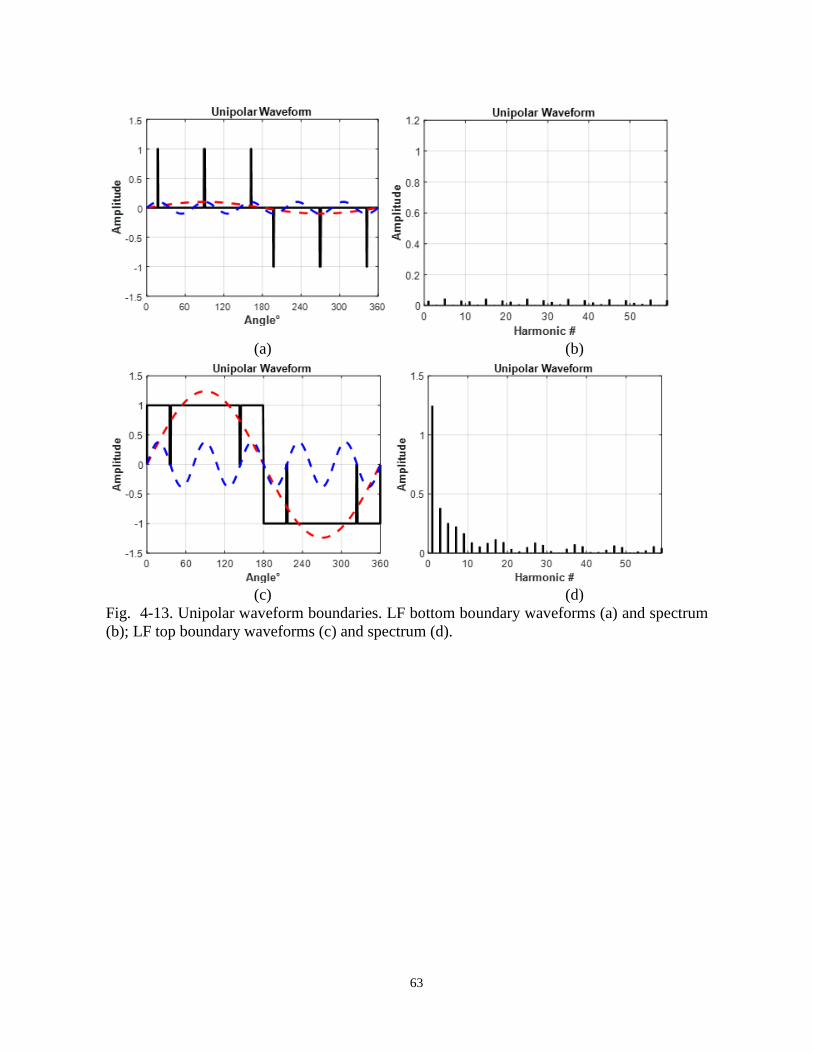
63
(a) (b)
(c) (d)
Fig. 4-13. Unipolar waveform boundaries. LF bottom boundary waveforms (a) and spectrum
(b); LF top boundary waveforms (c) and spectrum (d).
64
(a) (b)
(c) (d)
Fig. 4-14. Unipolar waveform and MFPWM waveforms. HF top boundary waveforms (a) and
spectrum (b) in a unipolar waveform; HF top boundary waveforms (c) and spectrum (d) in a
MFPWM waveform.

65
In summary, the constraints of the unipolar MFPWM includes 1) the LF can achieve 0-1 range,
but the HF restrains from 0-0.7 and further reduces if MiLF < 1. 2) the switching angle pattern is
restrained from 0-π/2 (0 ≤ 𝜃1 < ⋯ < 𝜃𝑚 ≤𝜋
2) in quarter-wave symmetric waveforms. 3) the
output boundary of the unipolar MFPWM is narrower than the single-output unipolar waveform,
as the switching angles of MFPWM suppress inter-harmonics.
In a bipolar waveform, the dominating LF contour breaks, and both LF and HF can reach their
maximum MiLF/MiHF ≈ 1.27, as shown in Fig. 4-15. The top boundary of LF is in Fig. 4-15(a) and
the top boundary of HF is in Fig. 4-15(c). However, tin both cases to maximize one element, the
other is reduced to zero. Due to the bipolar waveform, a minimal notch area still leads to a near
50% duty cycle square waveform and any additional notch area increases the HF element but
reduces LF amplitude.
In summary, the constraints of the bipolar MFPWM includes 1) the bipolar contour, resulting
in that the LF can achieve 0-1.27 range, but the HF restrains from 0.25-1.27. 2) 2) the switching
angle pattern is restrained from 0 - π/2 (0 ≤ 𝜃1 < ⋯ < 𝜃𝑚 ≤𝜋
2) in quarter-wave symmetric
waveforms. 3) the output boundary of the bipolar MFPWM is narrower than the single-output
bipolar waveform, as the switching angles of MFPWM suppress inter-harmonics.
As shown in the benchmark evaluation of SHE, the total switching angles has a non-linear
inverse impact on the both LF and HF modulation range. In Fig. 4-16, the modulation ranges of
MFPWM with 5/7 switching angles per quarter-wave are provided. In general, an increased
number of switching angles will narrow the modulation range, and this also depends on specific
operation points.
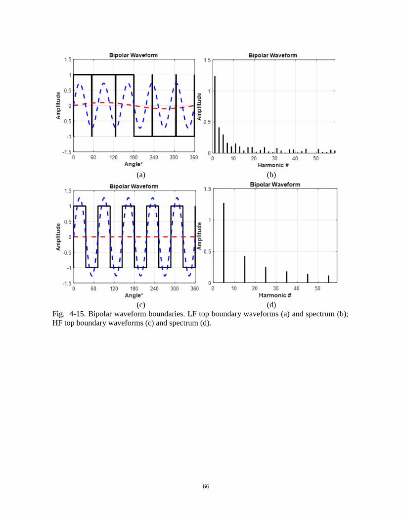
66
(a) (b)
(c) (d)
Fig. 4-15. Bipolar waveform boundaries. LF top boundary waveforms (a) and spectrum (b);
HF top boundary waveforms (c) and spectrum (d).
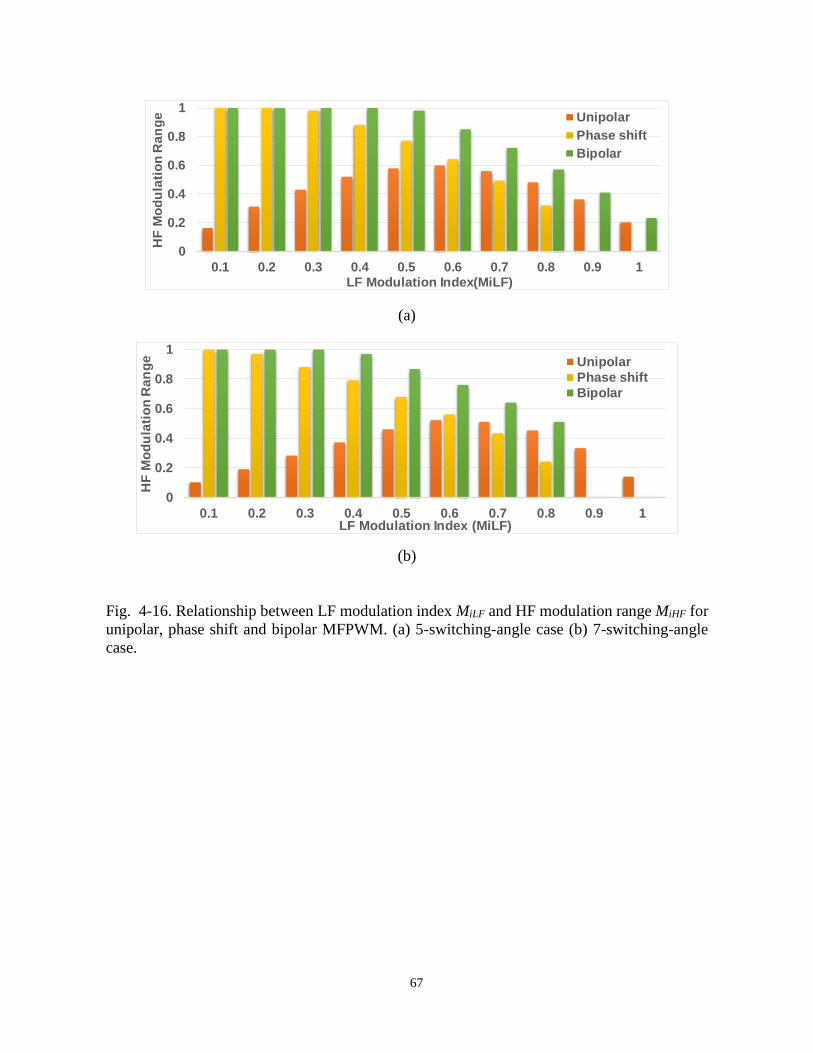
67
(a)
(b)
Fig. 4-16. Relationship between LF modulation index MiLF and HF modulation range MiHF for
unipolar, phase shift and bipolar MFPWM. (a) 5-switching-angle case (b) 7-switching-angle
case.
0
0.2
0.4
0.6
0.8
1
0.1 0.2 0.3 0.4 0.5 0.6 0.7 0.8 0.9 1
HF
Mo
du
lati
on
Ra
ng
e
LF Modulation Index(MiLF)
Unipolar
Phase shift
Bipolar
0
0.2
0.4
0.6
0.8
1
0.1 0.2 0.3 0.4 0.5 0.6 0.7 0.8 0.9 1
HF
Mo
du
lati
on
Ra
ng
e
LF Modulation Index (MiLF)
Unipolar
Phase shift
Bipolar

68
4.3.2 Switching loss
The switching loss depends on the total number of switching actions in each MFPWM
implementation. A waveform of MFPWM consists of m switching angles per quarter-wave, a finite
number of harmonics of the fundamental n = f(m) can be controlled, where n is a function of the
number of switching angles and the modulation scheme. For unipolar and bipolar MFPWM,
𝑛 = 2𝑚 − 1 (4-25)
where m > 1 is an odd integer. In a full bridge inverter configuration, unipolar MFPWM has a fast
switching phase leg and slow switching phase leg. However, both phase legs of bipolar MFPWM
are fast switching, resulting in different switching losses.
For unipolar MFPWM
𝑃𝑢𝑛𝑖_𝑀𝐹𝑃𝑊𝑀 = (2 ∙ 𝑄𝑔𝑠 ∙ 𝑉𝑔𝑠 + 2 ∙ 𝑄𝑜𝑠𝑠 ∙ 𝑉𝑑𝑐) ∙ (1 + 2𝑚 − 1) ∙ 𝑓𝐿𝐹 (4-26)
For bipolar MFPWM
𝑃𝑏𝑖_𝑀𝐹𝑃𝑊𝑀 = (4 ∙ 𝑄𝑔𝑠 ∙ 𝑉𝑔𝑠 + 4 ∙ 𝑄𝑜𝑠𝑠 ∙ 𝑉𝑑𝑐) ∙ (2𝑚 − 1) ∙ 𝑓𝐿𝐹 (4-27)
For phase-shift MFPWM, the addition 120° phase-shift between two phase legs cancels out all
triplen harmonics, and 𝑛 ∈ [1,5,7,11,13 … ] non-triplen odd harmonic. For instance, using 3
switching angles can control to the 7th harmonic and using 5 switching angles can control up to
17th harmonic. The switching loss is the same with the bipolar case.
𝑃𝑏𝑖_𝑀𝐹𝑃𝑊𝑀 = (4 ∙ 𝑄𝑔𝑠 ∙ 𝑉𝑔𝑠 + 4 ∙ 𝑄𝑜𝑠𝑠 ∙ 𝑉𝑑𝑐) ∙ (2𝑚 − 1) ∙ 𝑓𝐿𝐹 (4-28)
Among the three MFPWMs, the unipolar MFPWM has the lowest switching loss.
4.3.3 Harmonic content
The THD of an MFPWM waveform indicates the level of unregulated harmonic content above
the HF output. Those harmonics may cause circulating power flow and increase power loss if not
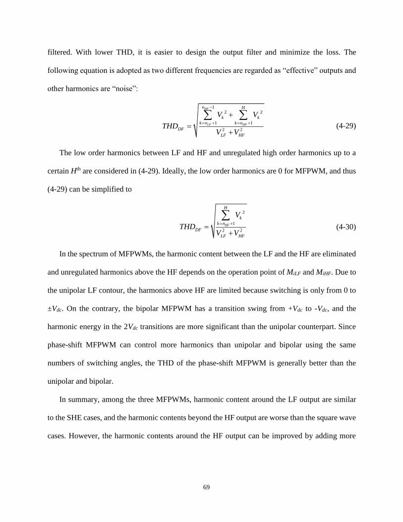
69
filtered. With lower THD, it is easier to design the output filter and minimize the loss. The
following equation is adopted as two different frequencies are regarded as “effective” outputs and
other harmonics are “noise”:
12 2
1 1
2 2
HF
LF HF
n H
k k
k n k n
DF
LF HF
V V
THDV V
(4-29)
The low order harmonics between LF and HF and unregulated high order harmonics up to a
certain Hth are considered in (4-29). Ideally, the low order harmonics are 0 for MFPWM, and thus
(4-29) can be simplified to
2
1
2 2
HF
H
k
k n
DF
LF HF
V
THDV V
(4-30)
In the spectrum of MFPWMs, the harmonic content between the LF and the HF are eliminated
and unregulated harmonics above the HF depends on the operation point of MiLF and MiHF. Due to
the unipolar LF contour, the harmonics above HF are limited because switching is only from 0 to
±Vdc. On the contrary, the bipolar MFPWM has a transition swing from +Vdc to -Vdc, and the
harmonic energy in the 2Vdc transitions are more significant than the unipolar counterpart. Since
phase-shift MFPWM can control more harmonics than unipolar and bipolar using the same
numbers of switching angles, the THD of the phase-shift MFPWM is generally better than the
unipolar and bipolar.
In summary, among the three MFPWMs, harmonic content around the LF output are similar
to the SHE cases, and the harmonic contents beyond the HF output are worse than the square wave
cases. However, the harmonic contents around the HF output can be improved by adding more

70
switching angles and extending the controllable range, and the performance will be close to the
carrier-based PWM and SHE cases.
4.3.4 Summary
A metric comparison of three MFPWMs is given in Table 4-3. The modulation range,
switching loss, harmonic content, and other metrics are compared. Three MFPWMs have distinct
advantages, and the selection depends on application priority. Compared with the benchmark
design, the proposed MFPWM has several advantages. 1) Only one inverter is needed for multiple
outputs. 2) the switching loss is lower than the carrier-based PWM and the conventional SHE. 3)
The low-order harmonics in between the LF and the HF are zero. The harmonics at HF output can
be reduced by adding switching actions. 4) Passive filter volume for low-order harmonics is
reduced.
4.4 MFPWM Extension
Three MFPWM schemes and their evaluations are presented in Section 4.2 and 4.3. To apply
the modulation to a wider range of applications, some extension studies of MFPWM are
investigated in this section. The number of switching angles in conventional SHE is limited to <
20 per quarter wave in past literature. In this dissertation, the MFPWM with > 30 switching angles
is investigated, which enables two output frequencies that are widely separated. In some
application, > 2 frequencies, or a combined output of multiple harmonics, rather than the
combination of the fundamental element and a kth harmonic are needed. Finally, a brief review of
the MFPWM in multilevel converters [100] is given in the section to extend the modulation to a
variety of topologies.

71
4.4.1 MFPWM with Extended Switching Angles
MFPWM with limited switching angles (m < 11) is discussed in Section 4.2 & 4.3. However,
sometimes it requires an extended range of multi-frequency generations [103][104]. Then, the set
of objective functions derived in Section 4.2 still apply and some examples are provided to verify
the feasibility of MFPWM with more than 30 switching angles.
To solve more than 30 non-linear transcendental equations, the Newton-Raphson iteration
algorithm is employed. However, more switching angles increase equation complexity, and
different initial values of this algorithm will influence the algorithm convergence. Direct derivation
of 35 initial values of this equation set is difficult, and thus an iterative initial value derivation
method is adopted. In this process, initial values for a smaller number of transcendental equations
are acquired first. Then the patterns of initial values are examined to gain qualitative insight into
the initial values for the full equation set from the reduced-order solutions. An example of the 35
initial values for the bipolar and the unipolar cases is given in Table 4-4 & Table 4-5.
TABLE. 4-3. METRIC COMPARISON OF THREE MFPWM
Unipolar Bipolar Phase-shift
LF Modulation range 0 – 1.27 0 – 1.27 0 – 1
HF Modulation range 0 – 0.76 0 – 1.27 0 – 1
Total switching loss 2m∙PLF 4 (m2-m) ∙ PLF 4 (m2-m) ∙ PLF
Harmonics in between
VLF and VHF zero zero zero
Adjacent harmonics
above VHF Low High Low
Inverter counts 1 1 1
Frequency
combination Odd harmonic Odd harmonics Non-triplen odd
harmonic
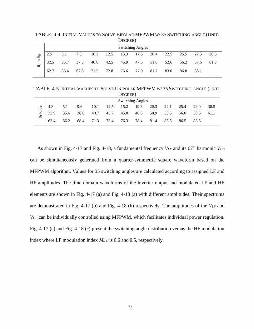
72
As shown in Fig. 4-17 and Fig. 4-18, a fundamental frequency VLF and its 67th harmonic VHF
can be simultaneously generated from a quarter-symmetric square waveform based on the
MFPWM algorithm. Values for 35 switching angles are calculated according to assigned LF and
HF amplitudes. The time domain waveforms of the inverter output and modulated LF and HF
elements are shown in Fig. 4-17 (a) and Fig. 4-18 (a) with different amplitudes. Their spectrums
are demonstrated in Fig. 4-17 (b) and Fig. 4-18 (b) respectively. The amplitudes of the VLF and
VHF can be individually controlled using MFPWM, which facilitates individual power regulation.
Fig. 4-17 (c) and Fig. 4-18 (c) present the switching angle distribution versus the HF modulation
index where LF modulation index MiLF is 0.6 and 0.5, respectively.
TABLE. 4-4. INITIAL VALUES TO SOLVE BIPOLAR MFPWM W/ 35 SWITCHING-ANGLE (UNIT:
DEGREE) θ
1 t
o θ
35
Switching Angles
2.5 5.1 7.5 10.2 12.5 15.3 17.5 20.4 22.5 25.5 27.5 30.6
32.5 35.7 37.5 40.8 42.5 45.9 47.5 51.0 52.6 56.2 57.6 61.3
62.7 66.4 67.8 71.5 72.8 76.6 77.9 81.7 83.0 86.8 88.1
TABLE. 4-5. INITIAL VALUES TO SOLVE UNIPOLAR MFPWM W/ 35 SWITCHING-ANGLE (UNIT:
DEGREE)
θ1 t
o θ
35
Switching Angles
4.8 5.1 9.6 10.1 14.5 15.2 19.3 20.3 24.1 25.4 29.0 30.5
33.9 35.6 38.8 40.7 43.7 45.8 48.6 50.9 53.5 56.0 58.5 61.1
63.4 66.2 68.4 71.3 73.4 76.3 78.4 81.4 83.5 86.5 88.5
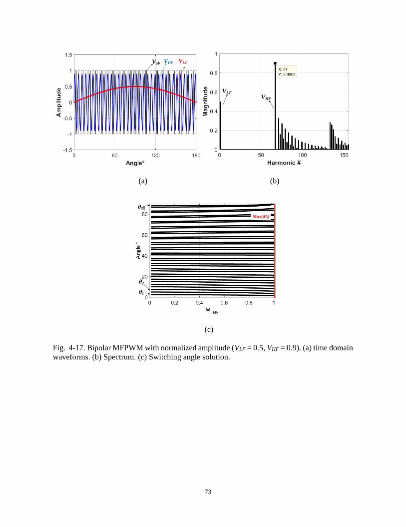
73
Vab VHF VLF
VLF
VHF
(a) (b)
θ1
θ2
θ35
Max(Mi)
(c)
Fig. 4-17. Bipolar MFPWM with normalized amplitude (VLF = 0.5, VHF = 0.9). (a) time domain
waveforms. (b) Spectrum. (c) Switching angle solution.
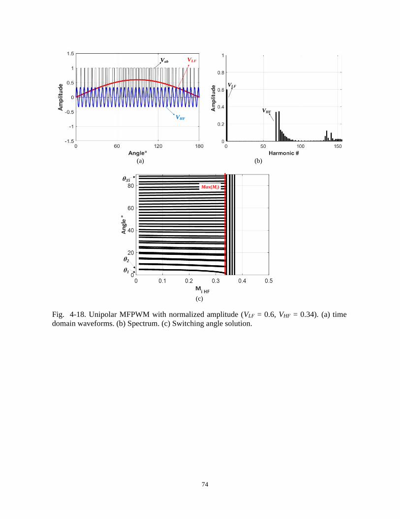
74
Vab
VHF
VLF
VLF
VHF
(a) (b)
θ1
θ2
θ35
Max(Mi)
(c)
Fig. 4-18. Unipolar MFPWM with normalized amplitude (VLF = 0.6, VHF = 0.34). (a) time
domain waveforms. (b) Spectrum. (c) Switching angle solution.
75
4.4.2 MFPWM with Flexible Output Combination
In Section 4.2, the proposed MFPWM generates two different frequencies as outputs, however,
more than two outputs are required in some cases. In addition, applications may regulate two
frequencies which are not multiples of one-ourther, preventing using the fundamental and its
harmonic. To apply MFPWM to meet the need of flexible output combination, MFPWM can be
tailored and some examples are given in this section.
A new set of objective functions for the bipolar MFPWM are:
1 2 1
1 2 2
1 2 3
1 2 4
1 2
4(1 2cos 2cos 2cos )
4(1 2cos3 2cos3 2cos3 )
3
4(1 2cos5 2cos5 2cos5 )
5
4(1 2cos 7 2cos 7 2cos 7 )
7
......
4(1 2cos cos 2cos )
dcm f
dcm f
dcm f
dcm f
dcm
f
VV
VV
VV
VV
Vn n n V
n
1
2
n
(4-31)
where Vfi ≥ 0.
In (4-30), the fundamental amplitude is Vf1. Its 3rd harmonic amplitude is Vf2 and the 5th
harmonic amplitude is Vf3. In this new MFPWM, the amplitude of each component is flexible. For
instance, the amplitude of fundamental frequency f1 can be set zero, as it is not used for output,
while the 3rd and the 7th harmonics are regulated to individual reference amplitudes. Moreover,
unemployed harmonics, such as the 5th and the 9th harmonics, can be eliminated to reduce cross-
interferences to adjacent channels. Finally, a certain range of high-order harmonics can be
suppressed by increasing switching angles up to nth, where n ≥ 7 in this case. An example of the
bipolar case is shown in Fig. 4-19.
76
A difference in unipolar case is that the fundamental amplitude Vf1 cannot be zero, to obtain
solutions from the numeric iteration algorithm. This fact is determined by the characteristic of the
unipolar waveforms, where the LF contour, Vf1, naturally forms the shape of the unipolar
modulation. If the fundamental component in a unipolar modulation is set to zero, then the inverter
output is Vab = 0 and no power will be delivered.
For unipolar MFPWM, the new objective functions are
1 2 1
1 2 2
1 2 3
1 2 4
1 2 1
2
4(cos cos cos )
4(cos3 cos3 cos3 )
3
4(cos5 cos5 cos5 )
5
4(cos 7 cos 7 cos 7 )
7
......
4(cos cos cos )
dcm f
dcm f
dcm f
dcm f
dcm n
f
VV
VV
VV
VV
Vn n n V
n
(4-32)
where Vfi ≥ 0.
This also results in the modulation range of the unipolar MFPWM boundary restrained, where
the HF modulation index MiHF cannot significantly exceed the fundamental modulation index MiLF.
The 3rd and 7th harmonics are employed for power delivery. As shown in Fig. 4-20, the fundamental
element Vfund is set 0.6Vdc to maximize modulation range of LF and HF components, VLF and VHF,
and the 3rd and 7th harmonics, VLF and VHF, are set to 0.35Vdc.
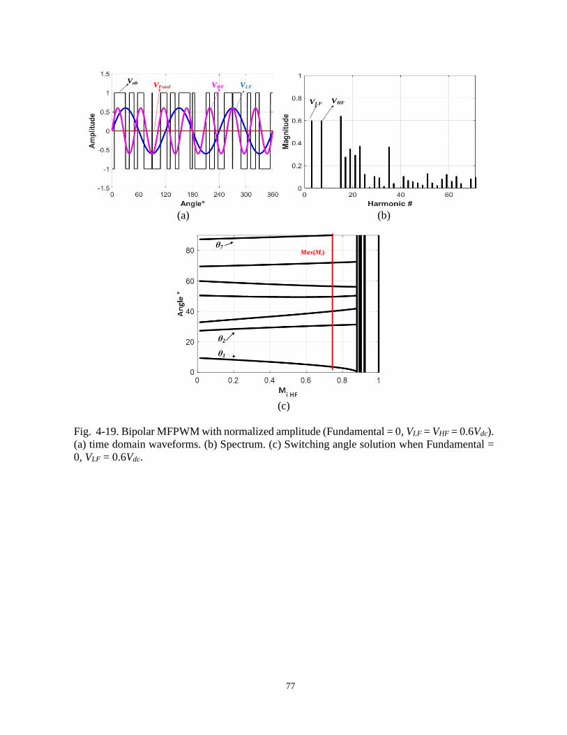
77
Vab VLFVFund VHF
VLF VHF
(a) (b)
θ1
θ2
θ7Max(Mi)
(c)
Fig. 4-19. Bipolar MFPWM with normalized amplitude (Fundamental = 0, VLF = VHF = 0.6Vdc).
(a) time domain waveforms. (b) Spectrum. (c) Switching angle solution when Fundamental =
0, VLF = 0.6Vdc.
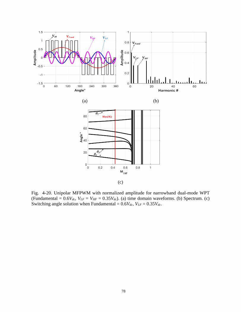
78
Vab VLFVFund VHF
VLF VHF
VFund
(a) (b)
θ1
θ2
θ7
Max(Mi)
(c)
Fig. 4-20. Unipolar MFPWM with normalized amplitude for narrowband dual-mode WPT
(Fundamental = 0.6Vdc, VLF = VHF = 0.35Vdc). (a) time domain waveforms. (b) Spectrum. (c)
Switching angle solution when Fundamental = 0.6Vdc, VLF = 0.35Vdc.
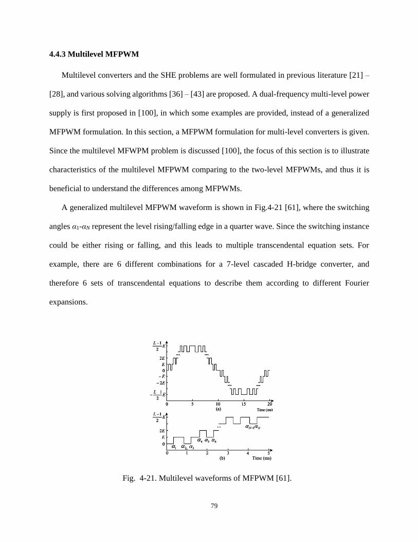
79
4.4.3 Multilevel MFPWM
Multilevel converters and the SHE problems are well formulated in previous literature [21] –
[28], and various solving algorithms [36] – [43] are proposed. A dual-frequency multi-level power
supply is first proposed in [100], in which some examples are provided, instead of a generalized
MFPWM formulation. In this section, a MFPWM formulation for multi-level converters is given.
Since the multilevel MFWPM problem is discussed [100], the focus of this section is to illustrate
characteristics of the multilevel MFPWM comparing to the two-level MFPWMs, and thus it is
beneficial to understand the differences among MFPWMs.
A generalized multilevel MFPWM waveform is shown in Fig.4-21 [61], where the switching
angles α1-αN represent the level rising/falling edge in a quarter wave. Since the switching instance
could be either rising or falling, and this leads to multiple transcendental equation sets. For
example, there are 6 different combinations for a 7-level cascaded H-bridge converter, and
therefore 6 sets of transcendental equations to describe them according to different Fourier
expansions.
Fig. 4-21. Multilevel waveforms of MFPWM [61].

80
A generalized set of transcendental equations for multilevel MFPWM is:
1 2
1 2
1 2
1 2
1 2
4( cos cos cos )
4( cos3 cos3 cos3 ) 0
3
4( cos5 cos5 cos5 ) 0
5
......
4( cos cos cos )
......
4( cos cos cos ) 0
dcm LF
dcm
dcm
dcm HF
dcm
VV
V
V
Vk k k V
k
Vn n n
n
where the positive/negative sign at each switching angles represents that it is a rising/falling edge
at that instance in a quarter-wave symmetry constraint. Using the numeric iteration, the
transcendental equations are solved. Some examples of dual-frequency generation can be found in
[100].
Considering the staircase multilevel waveforms, the modulation range of the LF output is 0-
M∙1.27, where M is the number of positive level. Also, the staircase waveform is naturally close
to a sinusoidal waveform at LF, and therefore the harmonic content is low compared to the unipolar
or bipolar waveforms. As a result, the modulation range of HF is even narrower than that in the
unipolar case. On the other hand, the THD of the multilevel MFPWM is lower than the two-level
MFPWM.
Compared to a full bridge converter, the voltage rating of each switching device in a multilevel
converter is reduced to 1/M, and the low-voltage rating devices have a lower Rds(on) and switching
loss, which may beneficial to improve the conversion efficiency. In summary, the multilevel

81
MFPWM may be advantageous for reducing THD, but are less suitable for dual-frequency output
due to a limited HF range.
4.4.4 Full Solution of MFPWM
As mentioned in the literature review, the SHE problem can be converted to a set of polynomial
equations, and then the roots of the polynomial equations are the switching angles. The solutions
of gradient-based algorithms using numeric iteration is largely determined by the initial condition,
and only one set of solution can be found. With the help of the conversion-based algorithms such
as polynomial equations, the full sets of MFPWM solutions are obtained.
A detailed algorithm description can be found in [75]-[78], and some results are reported in
this section. Using the Resultants Theory [75]-[77] and the Groebner Theory [78], the solutions of
the unipolar MFPWM and the bipolar MFPWM are identical to the results using numeric iteration.
Therefore, only one set of solutions exits for the unipolar and bipolar MFPWM. Also, attempts are
made for the multilevel MFWPM, and only one effective solution exists.
However, multiple solutions do exist in the phase-shift MFPWM, and some examples are given
in Fig. 4-22 and Fig. 4-23. A phase-shift MFPWM controlling the 1st -7th harmonics using 3
switching angles is shown in Fig. 4-22, and the fundamental frequency and the 7th harmonic are
two output frequency. Two solutions are given in Fig. 4-22(a) and (b). Solution 1 is found by
numeric iteration and solution 2 is found using polynomial equations. At the same operation point,
LF = 0.6 HF = 0.1, the unregulated harmonic content above the 10th of solution 2 is better than that
in solution 1. However, solution 2 has a very narrow HF range < 0.1, as shown in Fig. 4-22(f), and
this fact limits the usage of solution 2.
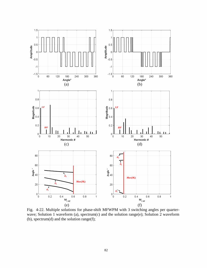
82
(a) (b)
LF
HF
LF
HF
(c) (d)
θ1
θ2
θ3
Max(Mi)
θ1
θ2
θ3
Max(Mi)
(e) (f)
Fig. 4-22. Multiple solutions for phase-shift MFWPM with 3 switching angles per quarter-
wave; Solution 1 waveform (a), spectrum(c) and the solution range(e); Solution 2 waveform
(b), spectrum(d) and the solution range(f);
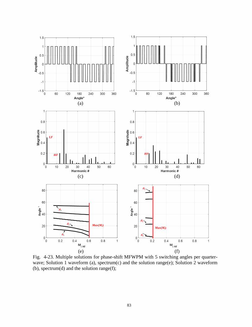
83
(a) (b)
LF
HF
LF
HF
(c) (d)
Max(Mi)
θ1
θ2
θ5
Max(Mi)
θ1
θ2
θ5
(e) (f)
Fig. 4-23. Multiple solutions for phase-shift MFWPM with 5 switching angles per quarter-
wave; Solution 1 waveform (a), spectrum(c) and the solution range(e); Solution 2 waveform
(b), spectrum(d) and the solution range(f);
84
A phase-shift MFPWM controlling the 1st -15th harmonics using 5 switching angles is shown
in Fig. 4-23, and similar results are obtained. In summary, though multiple solutions exist, a narrow
range of HF restrains the application of the additional solutions.
4.5 Conclusion
In this chapter, unipolar, bipolar and phase-shift MFPWM are investigated to simultaneously
generate two different frequencies from a single-phase full-bridge inverter, which facilitates power
regulation for multi-load ac applications. Compared with the benchmark design, MFPWM has
advantages on controlling harmonic content and reducing component count. Among three
MFPWMs, unipolar MFPWM has the lowest switching loss but the narrowest modulation range
of high frequency output. Bipolar MFPWM has the widest modulation range but the worst THD.
Phase-shift MFPWM can make a balance between improved THD and wide modulation range. In
addition, the proposed MFPWM is extended to other cases: widely separate frequency generations;
flexible output generation; and a multilevel MFWPM. A full solution using polynomial-
conversion-based algorithm is briefly discussed to provide a full coverage of this topic.
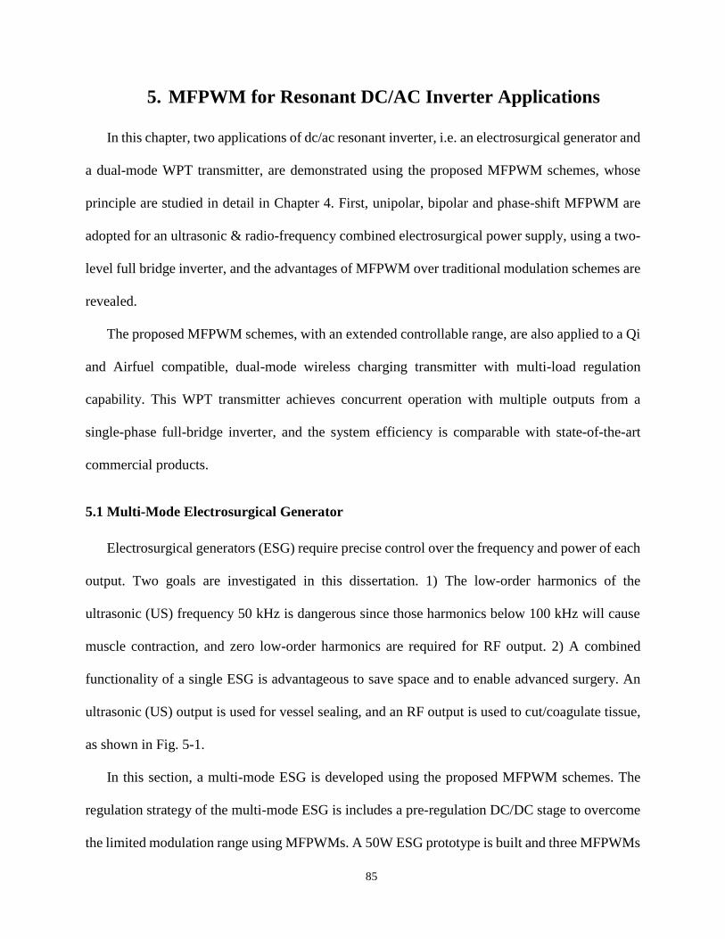
85
5. MFPWM for Resonant DC/AC Inverter Applications
In this chapter, two applications of dc/ac resonant inverter, i.e. an electrosurgical generator and
a dual-mode WPT transmitter, are demonstrated using the proposed MFPWM schemes, whose
principle are studied in detail in Chapter 4. First, unipolar, bipolar and phase-shift MFPWM are
adopted for an ultrasonic & radio-frequency combined electrosurgical power supply, using a two-
level full bridge inverter, and the advantages of MFPWM over traditional modulation schemes are
revealed.
The proposed MFPWM schemes, with an extended controllable range, are also applied to a Qi
and Airfuel compatible, dual-mode wireless charging transmitter with multi-load regulation
capability. This WPT transmitter achieves concurrent operation with multiple outputs from a
single-phase full-bridge inverter, and the system efficiency is comparable with state-of-the-art
commercial products.
5.1 Multi-Mode Electrosurgical Generator
Electrosurgical generators (ESG) require precise control over the frequency and power of each
output. Two goals are investigated in this dissertation. 1) The low-order harmonics of the
ultrasonic (US) frequency 50 kHz is dangerous since those harmonics below 100 kHz will cause
muscle contraction, and zero low-order harmonics are required for RF output. 2) A combined
functionality of a single ESG is advantageous to save space and to enable advanced surgery. An
ultrasonic (US) output is used for vessel sealing, and an RF output is used to cut/coagulate tissue,
as shown in Fig. 5-1.
In this section, a multi-mode ESG is developed using the proposed MFPWM schemes. The
regulation strategy of the multi-mode ESG is includes a pre-regulation DC/DC stage to overcome
the limited modulation range using MFPWMs. A 50W ESG prototype is built and three MFPWMs
86
are implemented to compare their performance. The effectiveness of MFPWM is verified by
experimental results which agree with the analysis in Chapter 4.
5.1.1 Implementation of Multi-mode ESG
In Chapter 4, three MFPWMs are investigated and their modulation range of LF and HF output
are revealed. In the ESG design, the LF is used for the US output and the HF is used for the RF
output. In the benchmark design using two independent inverters, both US and RF output can reach
0-1 modulation range. However, with a single inverter using MFPWMs, the US output ranges from
0 to 1, while the modulation range of the RF is limited, as shown in Chapter 4. To ensure RF output
modulation range from zero to one, a pre-regulation DC/DC stage is needed to regulate the inverter
input DC voltage Vbus, as shown in Fig. 5-2.
Fig. 5-1. An ultrasonic and radio frequency combined electrosurgical power supply.
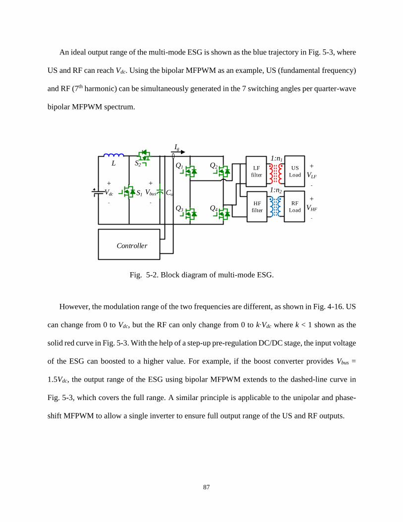
87
An ideal output range of the multi-mode ESG is shown as the blue trajectory in Fig. 5-3, where
US and RF can reach Vdc. Using the bipolar MFPWM as an example, US (fundamental frequency)
and RF (7th harmonic) can be simultaneously generated in the 7 switching angles per quarter-wave
bipolar MFPWM spectrum.
However, the modulation range of the two frequencies are different, as shown in Fig. 4-16. US
can change from 0 to Vdc, but the RF can only change from 0 to k∙Vdc where k < 1 shown as the
solid red curve in Fig. 5-3. With the help of a step-up pre-regulation DC/DC stage, the input voltage
of the ESG can boosted to a higher value. For example, if the boost converter provides Vbus =
1.5Vdc, the output range of the ESG using bipolar MFPWM extends to the dashed-line curve in
Fig. 5-3, which covers the full range. A similar principle is applicable to the unipolar and phase-
shift MFPWM to allow a single inverter to ensure full output range of the US and RF outputs.
RF
Load
+
Vdc
-
L
S1 Co
Q1 Q2
Q3 Q4
1:n1
1:n2
+
Vbus
-+
VHF
-
+
VLF
-
Ig
Controller
US
Load
S2LF
filter
HF
filter
Fig. 5-2. Block diagram of multi-mode ESG.
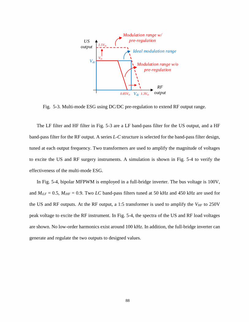
88
The LF filter and HF filter in Fig. 5-3 are a LF band-pass filter for the US output, and a HF
band-pass filter for the RF output. A series L-C structure is selected for the band-pass filter design,
tuned at each output frequency. Two transformers are used to amplify the magnitude of voltages
to excite the US and RF surgery instruments. A simulation is shown in Fig. 5-4 to verify the
effectiveness of the multi-mode ESG.
In Fig. 5-4, bipolar MFPWM is employed in a full-bridge inverter. The bus voltage is 100V,
and MiLF = 0.5, MiHF = 0.9. Two LC band-pass filters tuned at 50 kHz and 450 kHz are used for
the US and RF outputs. At the RF output, a 1:5 transformer is used to amplify the VHF to 250V
peak voltage to excite the RF instrument. In Fig. 5-4, the spectra of the US and RF load voltages
are shown. No low-order harmonics exist around 100 kHz. In addition, the full-bridge inverter can
generate and regulate the two outputs to designed values.
Vdc
Vdc
US
output
RF
output0.85Vdc 1.3Vdc
1.5Vdc
Vdc
Ideal modulation range
Modulation range w/
pre-regulation
Modulation range w/o
pre-regulation
Fig. 5-3. Multi-mode ESG using DC/DC pre-regulation to extend RF output range.
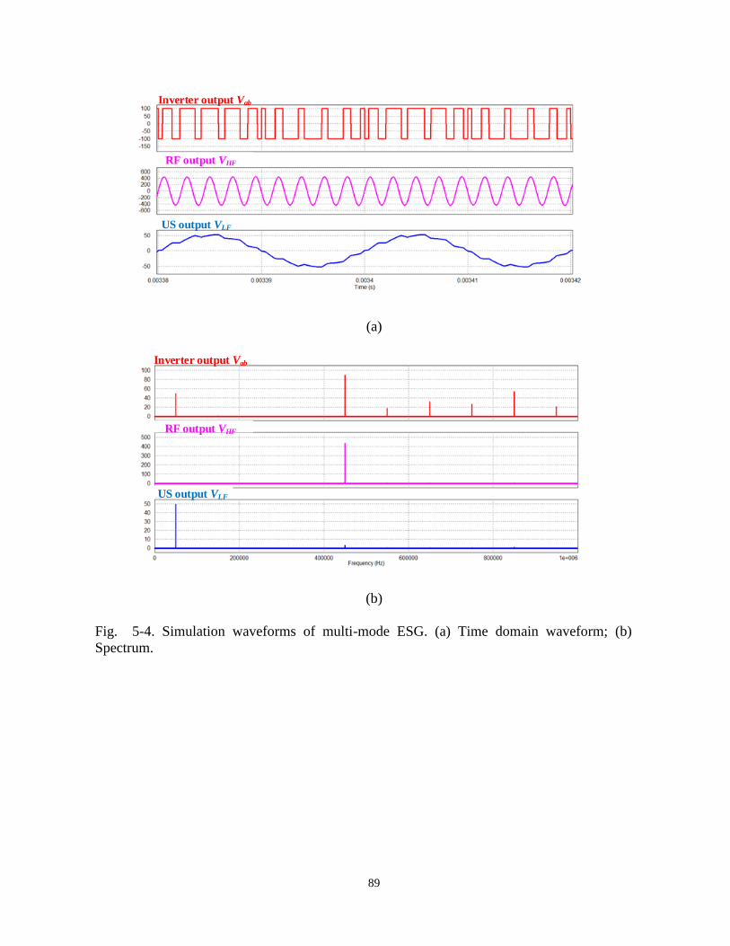
89
Inverter output Vab
RF output VHF
US output VLF
(a)
Inverter output Vab
RF output VHF
US output VLF
(b)
Fig. 5-4. Simulation waveforms of multi-mode ESG. (a) Time domain waveform; (b)
Spectrum.
90
5.1.2 Experimental results
To verify the effectiveness of the proposed MFPWMs for the multi-mode ESG, a full-bridge
inverter using Gallium-Nitride (GaN) devices is constructed. This prototype uses 50 kHz LF and
350 kHz HF frequency components to power two outputs simultaneously. To extract the LF and
HF elements from dual-frequency inverter output, two shunt LC filters connected to the inverter
output, and tuned at their individual resonant frequencies. The schematic circuit and test platform
are shown in Fig. 5-5. The parameters of the dual-frequency inverter are provided in Table 5-1.
The time domain waveforms and the spectra of the inverter output voltage are shown in Fig. 5-
6 – Fig. 5-8. The voltage waveforms of output voltage of the full bridge, Vab, the voltage of the LF
output, VLF, and the HF output, VHF, are given, and their spectrums are illustrated The experimental
waveforms sampled are from an MSO5104B oscilloscope and the FFT analysis is performed using
the oscilloscope.
From the FFT analysis directly on the oscilloscope, the RMS voltage value of the VLF is 42 V
from the Fig. 5-6 (b) – Fig. 5-8(b) and its peak value is 59V, whose normalized value is 0.59 and
is close to the prediction of 0.6. Also, the 5th harmonic is eliminated by MFPWM switching
instances. All triplen harmonics such as the 3rd, 9th and 15th are suppressed by the phase-shift case.
For the 5SA bipolar and unipolar MFPWM, as shown in Fig. 5-7 and Fig. 5-8, the 3rd, and 9th
harmonics are still within their harmonic control range,and can be eliminated by the MFPWM
modulation. However, other triplen harmonics above controllable band still exist, and they
contribute to the output THD.
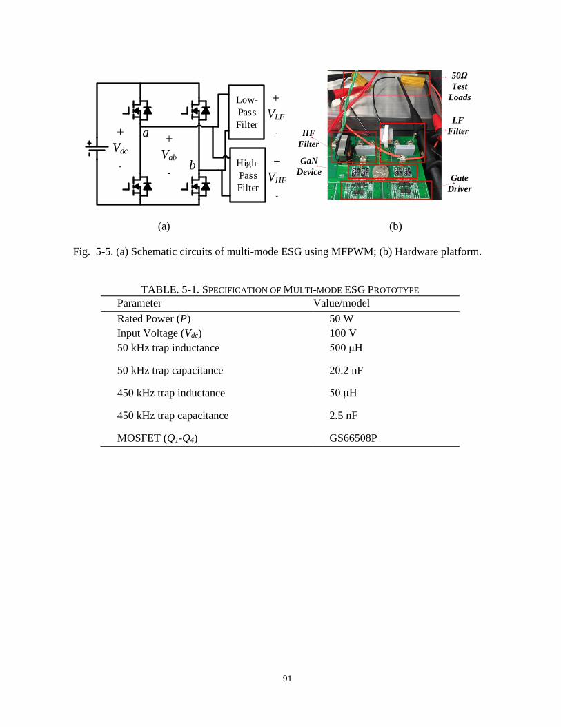
91
+
Vdc
-
+
Vab
-
a
b
Low-
Pass
Filter
High-
Pass
Filter
+
VLF
-
+
VHF
-
50Ω
Test
Loads
LF
Filter
Gate
Driver
HF
Filter
GaN
Device
(a) (b)
Fig. 5-5. (a) Schematic circuits of multi-mode ESG using MFPWM; (b) Hardware platform.
TABLE. 5-1. SPECIFICATION OF MULTI-MODE ESG PROTOTYPE
Parameter Value/model
Rated Power (P) 50 W
Input Voltage (Vdc) 100 V
50 kHz trap inductance 500 μH
50 kHz trap capacitance 20.2 nF
450 kHz trap inductance 50 μH
450 kHz trap capacitance 2.5 nF
MOSFET (Q1-Q4) GS66508P
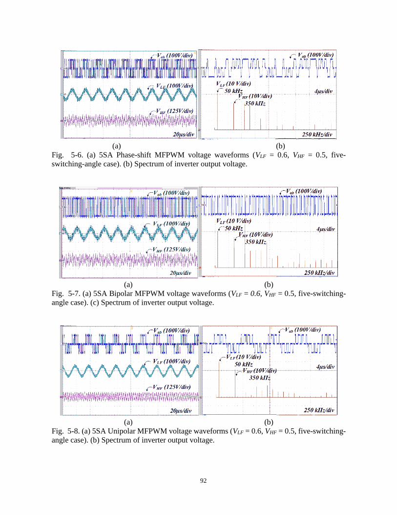
92
(a) (b)
Fig. 5-6. (a) 5SA Phase-shift MFPWM voltage waveforms (VLF = 0.6, VHF = 0.5, five-
switching-angle case). (b) Spectrum of inverter output voltage.
(a) (b)
Fig. 5-7. (a) 5SA Bipolar MFPWM voltage waveforms (VLF = 0.6, VHF = 0.5, five-switching-
angle case). (c) Spectrum of inverter output voltage.
(a) (b)
Fig. 5-8. (a) 5SA Unipolar MFPWM voltage waveforms (VLF = 0.6, VHF = 0.5, five-switching-
angle case). (b) Spectrum of inverter output voltage.
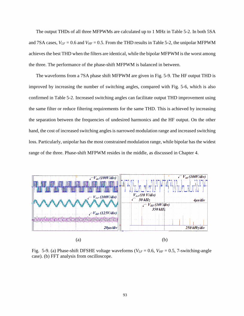
93
The output THDs of all three MFPWMs are calculated up to 1 MHz in Table 5-2. In both 5SA
and 7SA cases, VLF = 0.6 and VHF = 0.5. From the THD results in Table 5-2, the unipolar MFPWM
achieves the best THD when the filters are identical, while the bipolar MFPWM is the worst among
the three. The performance of the phase-shift MFPWM is balanced in between.
The waveforms from a 7SA phase shift MFPWM are given in Fig. 5-9. The HF output THD is
improved by increasing the number of switching angles, compared with Fig. 5-6, which is also
confirmed in Table 5-2. Increased switching angles can facilitate output THD improvement using
the same filter or reduce filtering requirements for the same THD. This is achieved by increasing
the separation between the frequencies of undesired harmonics and the HF output. On the other
hand, the cost of increased switching angles is narrowed modulation range and increased switching
loss. Particularly, unipolar has the most constrained modulation range, while bipolar has the widest
range of the three. Phase-shift MFPWM resides in the middle, as discussed in Chapter 4.
(a) (b)
Fig. 5-9. (a) Phase-shift DFSHE voltage waveforms (VLF = 0.6, VHF = 0.5, 7-switching-angle
case). (b) FFT analysis from oscilloscope.
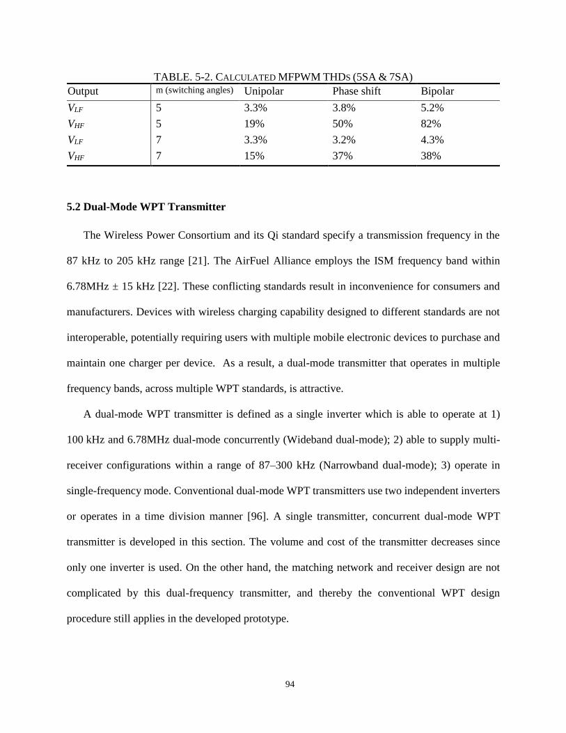
94
5.2 Dual-Mode WPT Transmitter
The Wireless Power Consortium and its Qi standard specify a transmission frequency in the
87 kHz to 205 kHz range [21]. The AirFuel Alliance employs the ISM frequency band within
6.78MHz ± 15 kHz [22]. These conflicting standards result in inconvenience for consumers and
manufacturers. Devices with wireless charging capability designed to different standards are not
interoperable, potentially requiring users with multiple mobile electronic devices to purchase and
maintain one charger per device. As a result, a dual-mode transmitter that operates in multiple
frequency bands, across multiple WPT standards, is attractive.
A dual-mode WPT transmitter is defined as a single inverter which is able to operate at 1)
100 kHz and 6.78MHz dual-mode concurrently (Wideband dual-mode); 2) able to supply multi-
receiver configurations within a range of 87–300 kHz (Narrowband dual-mode); 3) operate in
single-frequency mode. Conventional dual-mode WPT transmitters use two independent inverters
or operates in a time division manner [96]. A single transmitter, concurrent dual-mode WPT
transmitter is developed in this section. The volume and cost of the transmitter decreases since
only one inverter is used. On the other hand, the matching network and receiver design are not
complicated by this dual-frequency transmitter, and thereby the conventional WPT design
procedure still applies in the developed prototype.
TABLE. 5-2. CALCULATED MFPWM THDS (5SA & 7SA)
Output m (switching angles) Unipolar Phase shift Bipolar
VLF 5 3.3% 3.8% 5.2%
VHF 5 19% 50% 82%
VLF 7 3.3% 3.2% 4.3%
VHF 7 15% 37% 38%
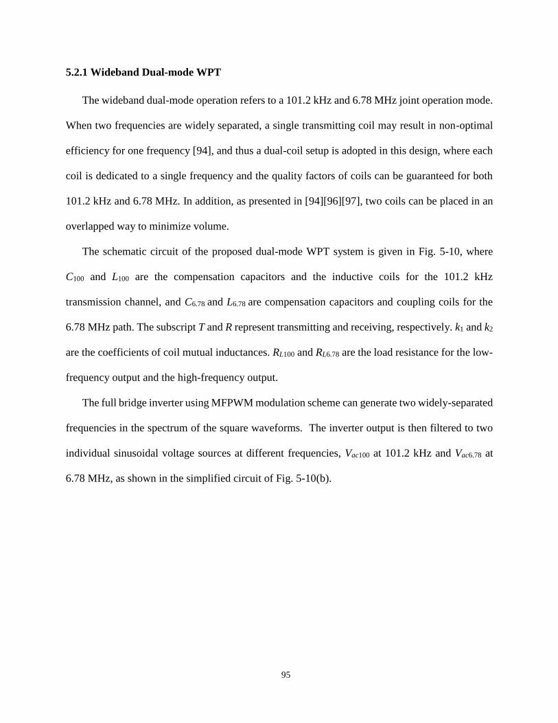
95
5.2.1 Wideband Dual-mode WPT
The wideband dual-mode operation refers to a 101.2 kHz and 6.78 MHz joint operation mode.
When two frequencies are widely separated, a single transmitting coil may result in non-optimal
efficiency for one frequency [94], and thus a dual-coil setup is adopted in this design, where each
coil is dedicated to a single frequency and the quality factors of coils can be guaranteed for both
101.2 kHz and 6.78 MHz. In addition, as presented in [94][96][97], two coils can be placed in an
overlapped way to minimize volume.
The schematic circuit of the proposed dual-mode WPT system is given in Fig. 5-10, where
C100 and L100 are the compensation capacitors and the inductive coils for the 101.2 kHz
transmission channel, and C6.78 and L6.78 are compensation capacitors and coupling coils for the
6.78 MHz path. The subscript T and R represent transmitting and receiving, respectively. k1 and k2
are the coefficients of coil mutual inductances. RL100 and RL6.78 are the load resistance for the low-
frequency output and the high-frequency output.
The full bridge inverter using MFPWM modulation scheme can generate two widely-separated
frequencies in the spectrum of the square waveforms. The inverter output is then filtered to two
individual sinusoidal voltage sources at different frequencies, Vac100 at 101.2 kHz and Vac6.78 at
6.78 MHz, as shown in the simplified circuit of Fig. 5-10(b).
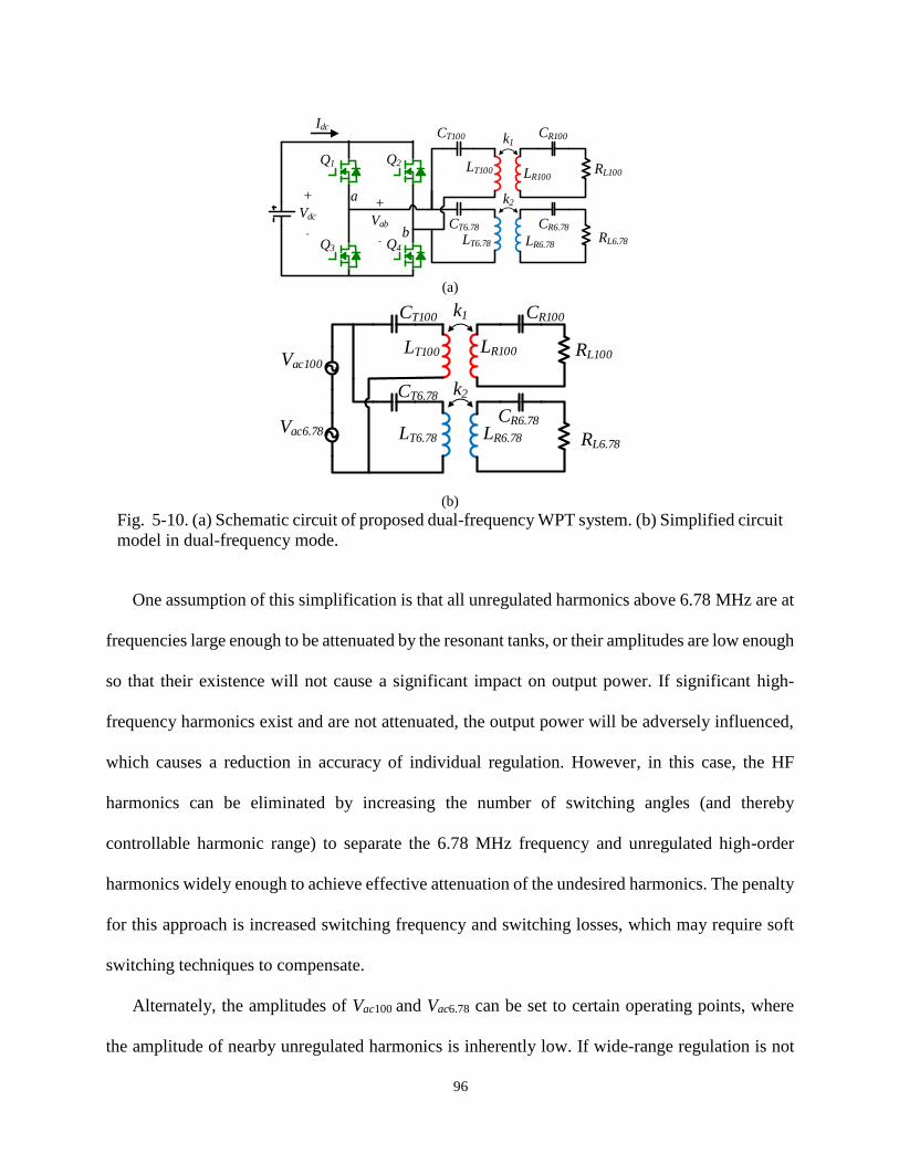
96
One assumption of this simplification is that all unregulated harmonics above 6.78 MHz are at
frequencies large enough to be attenuated by the resonant tanks, or their amplitudes are low enough
so that their existence will not cause a significant impact on output power. If significant high-
frequency harmonics exist and are not attenuated, the output power will be adversely influenced,
which causes a reduction in accuracy of individual regulation. However, in this case, the HF
harmonics can be eliminated by increasing the number of switching angles (and thereby
controllable harmonic range) to separate the 6.78 MHz frequency and unregulated high-order
harmonics widely enough to achieve effective attenuation of the undesired harmonics. The penalty
for this approach is increased switching frequency and switching losses, which may require soft
switching techniques to compensate.
Alternately, the amplitudes of Vac100 and Vac6.78 can be set to certain operating points, where
the amplitude of nearby unregulated harmonics is inherently low. If wide-range regulation is not
Q1 Q2
Q3 Q4
+
Vdc
-
Idc
+
Vab
-
a
b
CT100
LT100 LR100RL100
RL6.78
CR100
CT6.78
LT6.78
CR6.78
LR6.78
k1
k2
(a)
CT100
LT100 LR100 RL100
RL6.78
CR100
CT6.78
LT6.78
CR6.78
LR6.78
k1
k2
Vac100
Vac6.78
(b)
Fig. 5-10. (a) Schematic circuit of proposed dual-frequency WPT system. (b) Simplified circuit
model in dual-frequency mode.
97
necessary, unipolar MFPWM can be adopted instead of bipolar to take advantage of low content
of high-order harmonics. In this case, only one phase leg will operate at an equivalent switching
frequency of 6.78 MHz while another phase leg will switch complementarily at 101.2 kHz using
unipolar MFPWM in a full bridge configuration.
When multiple frequencies are present in the same transmitter, one frequency may be picked
up by a non-targeted receiver tuned at a different frequency, if the two frequencies are very close
or the quality factor of the coils is low [94]. The influence of each of the two frequencies on
adjacent power transfer channels is examined using separate circuit models, as shown in Fig. 5-11
(a). These models use superposition to examine the two power transfer frequencies individually,
assuming nearly zero output impedance from the inverter.
The input impedance of the 6.78 MHz channel shown to the 101.2 kHz voltage source is
CT100
LT100 LR100
RL100
CR100k1
Vac100
ZT6.78
RL6.78
CT6.78
LT6.78
CR6.78
LR6.78
k2
Vac6.78
ZT100
(a)
(b)
Fig. 5-11. (a) Simplified circuit model using superposition method. (b) voltage gains of two
channels. (k1 = k2 = 0.1).
98
6.78 100 6.78 6.78 6.78
100 6.78
1T T ref
T
Z j L R Zj C
(5-1)
where R100 and R6.78 are the parasitic resistance of the coil, and the Zref6.78 is the reflected impedance
from secondary side,
2
100 2 6.78 6.78
6.78
100 6.78 100 6.78 6.78 6.781
T R
ref
R R L
k L LZ
j L j C R R
(5-2)
As an example, a coil design specifies the inductance value of the 6.78 MHz coil as 1µH and
the compensation capacitance around 550 pF. Therefore, ZT6.78 can be approximated as a large
capacitive impedance at 101.2 kHz, which will block the 101.2 kHz voltage source and thereby
the circulating current in the high-frequency network will be largely suppressed.
The impedance ZT100 of the 101.2 kHz channel presented to the 6.78 MHz source is
100 6.78 100 100 100
6.78 100
1T T ref
T
Z j L R Zj C
(5-3)
2
6.78 1 100 100
100
6.78 100 6.78 100 100 1001
T R
ref
R R L
k L LZ
j L j C R R
(5-4)
The inductance of the transmitting coil of the 101.2 kHz channel is selected as 24 µH to
maintain a quality factor around 100, as suggested in the Qi standard [21]. As a result, ZT100 will
present a large inductive impedance to the 6.78 MHz source so that circulating current in the 100-
kHz channel is also minimal. The frequency sweep of two power channels is demonstrated in Fig.
5-11 (b), where the Y-axis represents the voltage gain from the load voltage to the input dc voltage.
Fig. 5-11 (b) demonstrates that each power channel achieves high voltage gain at its individual
resonant frequency while suppressing the other. Since the selected frequencies are widely
separated, by over one decade, and the quality factor of the 101.2 kHz coils and the 6.78 MHz
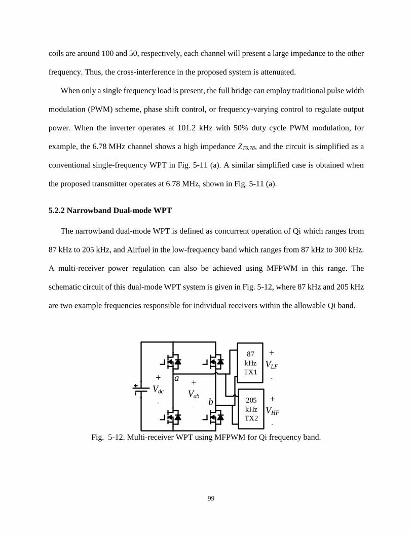
99
coils are around 100 and 50, respectively, each channel will present a large impedance to the other
frequency. Thus, the cross-interference in the proposed system is attenuated.
When only a single frequency load is present, the full bridge can employ traditional pulse width
modulation (PWM) scheme, phase shift control, or frequency-varying control to regulate output
power. When the inverter operates at 101.2 kHz with 50% duty cycle PWM modulation, for
example, the 6.78 MHz channel shows a high impedance ZT6.78, and the circuit is simplified as a
conventional single-frequency WPT in Fig. 5-11 (a). A similar simplified case is obtained when
the proposed transmitter operates at 6.78 MHz, shown in Fig. 5-11 (a).
5.2.2 Narrowband Dual-mode WPT
The narrowband dual-mode WPT is defined as concurrent operation of Qi which ranges from
87 kHz to 205 kHz, and Airfuel in the low-frequency band which ranges from 87 kHz to 300 kHz.
A multi-receiver power regulation can also be achieved using MFPWM in this range. The
schematic circuit of this dual-mode WPT system is given in Fig. 5-12, where 87 kHz and 205 kHz
are two example frequencies responsible for individual receivers within the allowable Qi band.
+
Vdc
-
+
Vab
-
a
b
87
kHz
TX1
205
kHz
TX2
+
VLF
-
+
VHF
-
Fig. 5-12. Multi-receiver WPT using MFPWM for Qi frequency band.

100
However, it will fall outside the allowable Qi bands if employing a combination of a
fundamental frequency and an odd harmonic. For example, the low-end frequency of the Qi
standard is 87 kHz, and its 3rd harmonic is 261 kHz, which exceeds the high-end frequency of 205
kHz in Qi specification. In order to comply with the Qi standard and obtain a flexible selection of
frequencies, the MFPWM scheme presented in Section 4.4.2 is employed here, instead of the
MFPWM in Section 5.1. A combination of multiple harmonics is selected, and the fundamental
frequency is not used for power transfer. Instead, the selected harmonic frequencies are used for
multi-receiver power deliveries. For example, using a fundamental frequency of 29 kHz, its 3rd
harmonic is 87 kHz and 7th harmonic is less than 205 kHz, both within the allowable range.
Therefore, the 3rd and 7th harmonics that transfer power are within the Qi band, while the
fundamental frequency amplitude is controlled to zero, or attenuated by the band-pass filters.
The circuit model of narrowband dual-mode WPT using MFPWM is shown in Fig. 5-13 (a).
In the circuit model, subscript number 29, 87 and 205 represent the frequencies of 29 kHz, 87 kHz
and 205 kHz respectively. A frequency sweep of the voltage gains in the two channels is given in
Fig. 5-13 (b). For this plot, the 87 kHz coils are modeled after a commercial coil design, with
24 µH inductance and a quality factor of 100; the 205 kHz coils are hand wounded with 26 µH
inductance and a quality factor of 50. The two channels exhibit -65dB and -40 dB for non-targeted
frequencies to suppress cross-regulation issue.
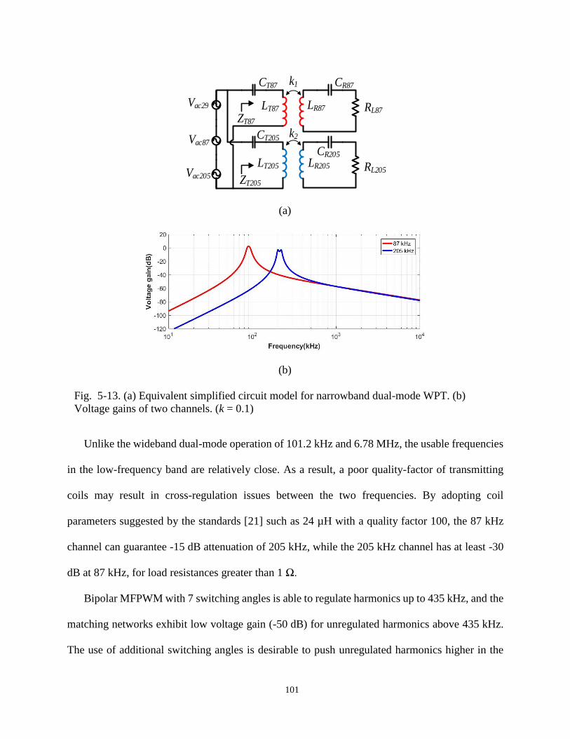
101
Unlike the wideband dual-mode operation of 101.2 kHz and 6.78 MHz, the usable frequencies
in the low-frequency band are relatively close. As a result, a poor quality-factor of transmitting
coils may result in cross-regulation issues between the two frequencies. By adopting coil
parameters suggested by the standards [21] such as 24 µH with a quality factor 100, the 87 kHz
channel can guarantee -15 dB attenuation of 205 kHz, while the 205 kHz channel has at least -30
dB at 87 kHz, for load resistances greater than 1 Ω.
Bipolar MFPWM with 7 switching angles is able to regulate harmonics up to 435 kHz, and the
matching networks exhibit low voltage gain (-50 dB) for unregulated harmonics above 435 kHz.
The use of additional switching angles is desirable to push unregulated harmonics higher in the
CT87
LT87 LR87 RL87
RL205
CR87
CT205
LT205
CR205
LR205
k1
k2Vac87
Vac205
Vac29
ZT87
ZT205
(a)
(b)
Fig. 5-13. (a) Equivalent simplified circuit model for narrowband dual-mode WPT. (b)
Voltage gains of two channels. (k = 0.1)
102
spectrum where the matching networks have larger attenuation. For unipolar MFPWM, however,
both channels are not only required to suppress unregulated harmonics but also are demanded to
attenuate the unavoidable fundamental component. In Fig. 5-13 (b), the gain at 29 kHz in two
channels are -60dB and -95 dB; the high impedances suppress the undesired fundamental
component.
As a result, the narrowband dual-mode WPT, or the multi-receiver regulation in the Qi standard,
can be achieved solely by assigned dedicated frequencies, while other frequencies in the spectrum
are attenuated by the band-pass filtering of two resonant networks. Designing at different
frequencies for multiple receivers within the Qi standard and/or the low-frequency Airfuel band
can be accomplished using the same principles.
5.2.3 Experimental Results
A Gallium Nitride (GaN)-based inverter is constructed using Navitas 6131 to support high-
frequency operation up to 6.78 MHz. The gate drivers are Si8273 from Silicon labs with 200kV/µs
common-mode immunity. Considering the control resolution and cycle by cycle response for high-
frequency operation, an ALTERA Cyclone IV FPGA controller with 300 MHz system clock is
used to generate the programmed MFPWM signals. The pre-determined switching angles are
calculated offline using MATLAB software. The system setup is demonstrated in Fig. 5-14 and
the prototype specifications are listed in Table 5-3. Using the same hardware, but varying coils
and matching networks, both dual-mode wideband and narrowband WPT are tested.
First, the setup is used to test wideband dual-mode operation at 101.2 kHz and 6.78 MHz. For
the 101.2 kHz power transfer channel, the coils are implemented Wurth Electronics Inc. WPCC
Wireless Power Charging Coils, which have a quality factor of 100 at 101.2 kHz. The 6.78 MHz
coils are hand wound with a lower quality factor of 50 at the operation frequency. The coil design
103
is not the focus of this dissertation, and advanced coil design techniques, such as in [96][97] are
applicable to this dual-mode WPT system to enhance the system efficiency.
Experimental voltage waveforms of the inverter output and load voltages at the 101.2 kHz and
6.78 MHz receiver are given in Fig. 5-15 (b). In Fig. 5-15 (a), the zoomed-in inverter output voltage
and its spectrum are shown, where the amplitude (relative to the dc bus voltage) of VLF is set to
0.5Vdc and that of VHF is set to 0.9Vdc. The dc bus voltage is 20V and load power reaches 12 W.
The voltage spectrum amplitudes in Fig. 5-15 (a) are RMS values. In Fig. 5-16, an alternate set of
switching angles is used to obtain the equal amplitude of VLF and VHF at 0.6Vdc, where the dc input
voltage is 10 V. In a real application, by adjusting the amplitude of each frequency to desired
values, the individual output powers of each channel can be regulated. Multiple sets of switching
angles can be calculated offline and then stored in the controller, so that the controller will not be
required to solve transcendental equations.
There are some unregulated harmonics above 6.78 MHz in Fig. 5-15 and Fig. 5-16 that result
in distortion of the load voltages, which are expected by design, and reside in the unregulated
region of the spectrum. This distortion can be suppressed by selecting certain operating points
where adjacent harmonic content is inherently low (e.g. MiLF = 0.5, MiHF = 0.9) or by increasing
switching angles, as discussed in Chapter 4. A different operating point (MiLF = 0.5, MiHF = 0.9) is
shown in Fig. 5-17 (a), where the fundamental frequency is set at 205.5 kHz and its 33rd harmonic
is 6.78 MHz. The range of nulled harmonics extends above 6.78 MHz. The normalized amplitude
of the 205.5 kHz component is set to 0.5 and that of the 6.78 MHz component is set to 0.9. In Fig.
5-17 (b), the inverter output, 205.5 kHz and 6.78 MHz load voltages are measured. Harmonics are
attenuated at the 6.78 MHz load, and output power reaches 10 W.
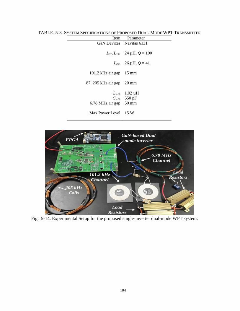
104
TABLE. 5-3. SYSTEM SPECIFICATIONS OF PROPOSED DUAL-MODE WPT TRANSMITTER Item Parameter
GaN Devices Navitas 6131
L87, L100 24 µH, Q = 100
L205 26 µH, Q = 41
101.2 kHz air gap 15 mm
87, 205 kHz air gap 20 mm
L6.78 1.02 µH
C6.78 550 pF
6.78 MHz air gap 50 mm
Max Power Level 15 W
GaN-based Dual
mode inverterFPGA
6.78 MHz
Channel
101.2 kHz
Channel
205 kHz
Coils
Load
Resistors
Load
Resistors
Fig. 5-14. Experimental Setup for the proposed single-inverter dual-mode WPT system.
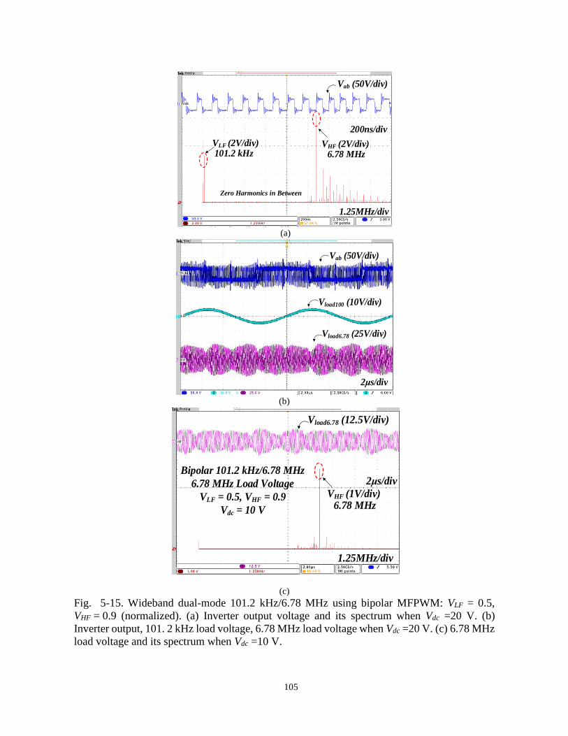
105
Vab (50V/div)
200ns/div
VHF (2V/div)VLF (2V/div)
1.25MHz/div
101.2 kHz 6.78 MHz
Zero Harmonics in Between
(a)
Vab (50V/div)
Vload100 (10V/div)
Vload6.78 (25V/div)
2μs/div
(b)
Vload6.78 (12.5V/div)
VHF (1V/div)6.78 MHz
2μs/div
1.25MHz/div
Bipolar 101.2 kHz/6.78 MHz
6.78 MHz Load Voltage
VLF = 0.5, VHF = 0.9
Vdc = 10 V
(c)
Fig. 5-15. Wideband dual-mode 101.2 kHz/6.78 MHz using bipolar MFPWM: VLF = 0.5,
VHF = 0.9 (normalized). (a) Inverter output voltage and its spectrum when Vdc =20 V. (b)
Inverter output, 101. 2 kHz load voltage, 6.78 MHz load voltage when Vdc =20 V. (c) 6.78 MHz
load voltage and its spectrum when Vdc =10 V.
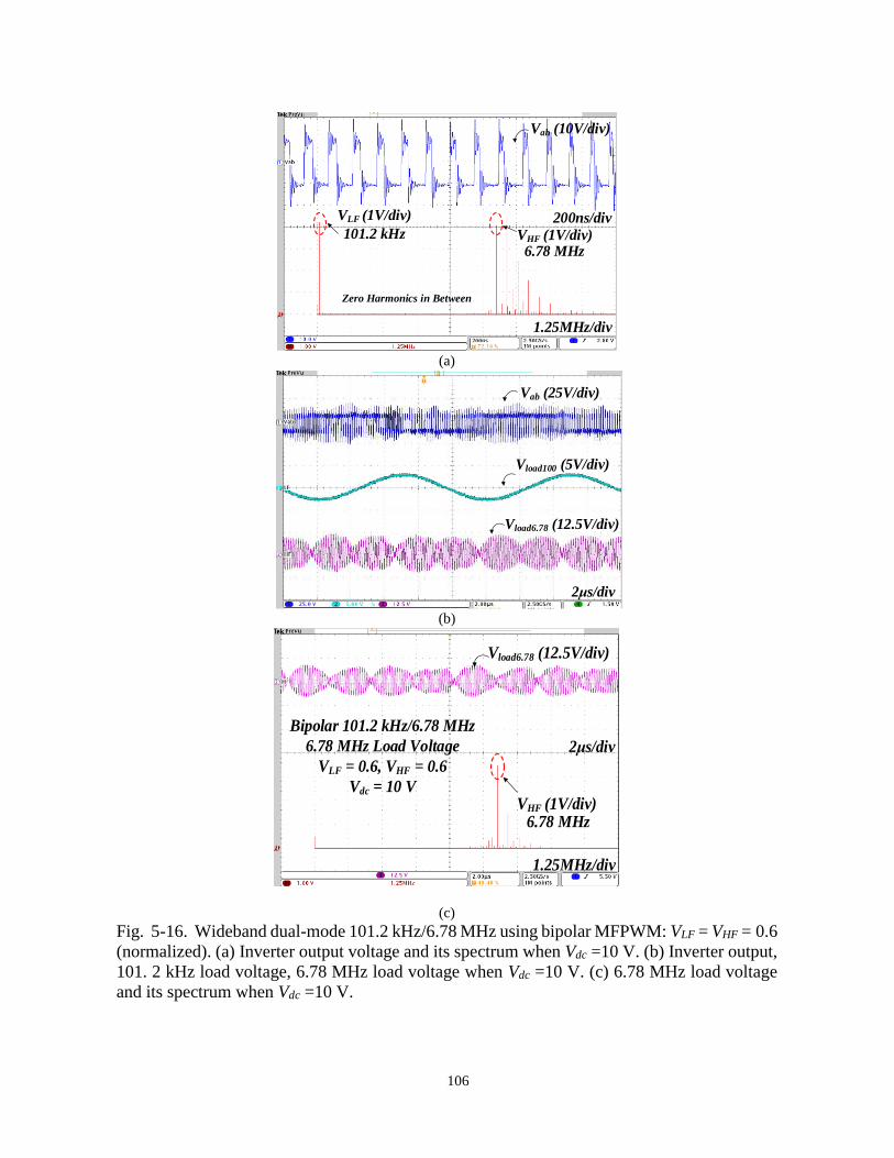
106
Vab (10V/div)
200ns/div
VHF (1V/div)
VLF (1V/div)
1.25MHz/div
101.2 kHz
6.78 MHz
Zero Harmonics in Between
(a)
Vab (25V/div)
Vload100 (5V/div)
Vload6.78 (12.5V/div)
2μs/div
(b)
Vload6.78 (12.5V/div)
VHF (1V/div)6.78 MHz
2μs/div
1.25MHz/div
Bipolar 101.2 kHz/6.78 MHz
6.78 MHz Load Voltage
VLF = 0.6, VHF = 0.6
Vdc = 10 V
(c)
Fig. 5-16. Wideband dual-mode 101.2 kHz/6.78 MHz using bipolar MFPWM: VLF = VHF = 0.6
(normalized). (a) Inverter output voltage and its spectrum when Vdc =10 V. (b) Inverter output,
101. 2 kHz load voltage, 6.78 MHz load voltage when Vdc =10 V. (c) 6.78 MHz load voltage
and its spectrum when Vdc =10 V.
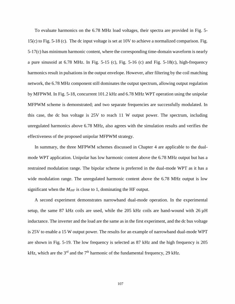
107
To evaluate harmonics on the 6.78 MHz load voltages, their spectra are provided in Fig. 5-
15(c) to Fig. 5-18 (c). The dc input voltage is set at 10V to achieve a normalized comparison. Fig.
5-17(c) has minimum harmonic content, where the corresponding time-domain waveform is nearly
a pure sinusoid at 6.78 MHz. In Fig. 5-15 (c), Fig. 5-16 (c) and Fig. 5-18(c), high-frequency
harmonics result in pulsations in the output envelope. However, after filtering by the coil matching
network, the 6.78 MHz component still dominates the output spectrum, allowing output regulation
by MFPWM. In Fig. 5-18, concurrent 101.2 kHz and 6.78 MHz WPT operation using the unipolar
MFPWM scheme is demonstrated; and two separate frequencies are successfully modulated. In
this case, the dc bus voltage is 25V to reach 11 W output power. The spectrum, including
unregulated harmonics above 6.78 MHz, also agrees with the simulation results and verifies the
effectiveness of the proposed unipolar MFPWM strategy.
In summary, the three MFPWM schemes discussed in Chapter 4 are applicable to the dual-
mode WPT application. Unipolar has low harmonic content above the 6.78 MHz output but has a
restrained modulation range. The bipolar scheme is preferred in the dual-mode WPT as it has a
wide modulation range. The unregulated harmonic content above the 6.78 MHz output is low
significant when the MiHF is close to 1, dominating the HF output.
A second experiment demonstrates narrowband dual-mode operation. In the experimental
setup, the same 87 kHz coils are used, while the 205 kHz coils are hand-wound with 26 µH
inductance. The inverter and the load are the same as in the first experiment, and the dc bus voltage
is 25V to enable a 15 W output power. The results for an example of narrowband dual-mode WPT
are shown in Fig. 5-19. The low frequency is selected as 87 kHz and the high frequency is 205
kHz, which are the 3rd and the 7th harmonic of the fundamental frequency, 29 kHz.
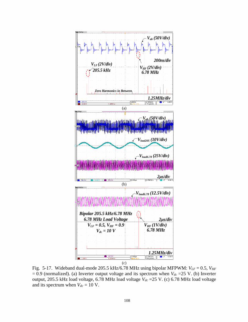
108
Vab (50V/div)
200ns/div
VHF (2V/div)VLF (2V/div)
1.25MHz/div
205.5 kHz 6.78 MHz
Zero Harmonics in Between
(a)
Vab (50V/div)
Vload205 (10V/div)
Vload6.78 (25V/div)
2μs/div
(b)
Vload6.78 (12.5V/div)
VHF (1V/div)6.78 MHz
2μs/div
1.25MHz/div
Bipolar 205.5 kHz/6.78 MHz
6.78 MHz Load Voltage
VLF = 0.5, VHF = 0.9
Vdc = 10 V
(c)
Fig. 5-17. Wideband dual-mode 205.5 kHz/6.78 MHz using bipolar MFPWM: VLF = 0.5, VHF
= 0.9 (normalized). (a) Inverter output voltage and its spectrum when Vdc =25 V. (b) Inverter
output, 205.5 kHz load voltage, 6.78 MHz load voltage Vdc =25 V. (c) 6.78 MHz load voltage
and its spectrum when Vdc = 10 V.
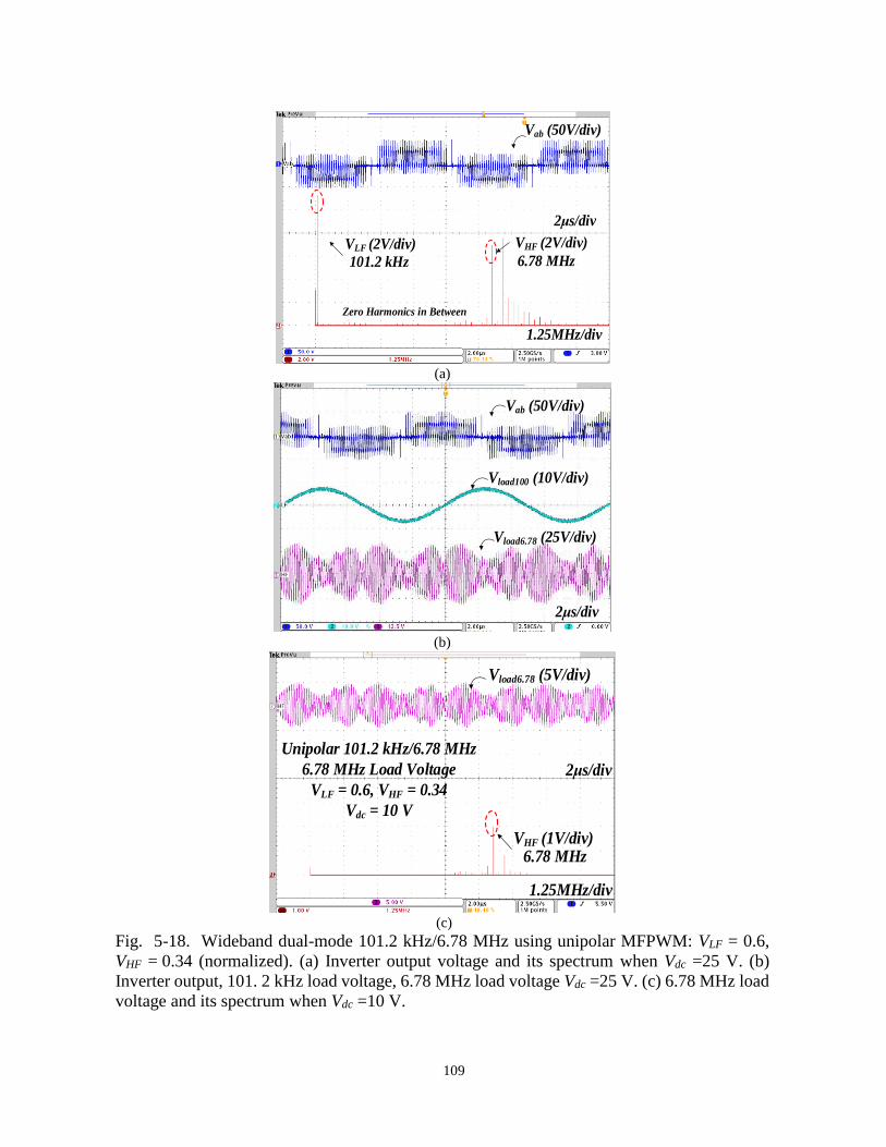
109
Vab (50V/div)
VHF (2V/div)VLF (2V/div)
1.25MHz/div
101.2 kHz 6.78 MHz
2μs/div
Zero Harmonics in Between
(a)
Vab (50V/div)
Vload100 (10V/div)
Vload6.78 (25V/div)
2μs/div
(b)
Vload6.78 (5V/div)
VHF (1V/div)6.78 MHz
2μs/div
1.25MHz/div
Unipolar 101.2 kHz/6.78 MHz
6.78 MHz Load Voltage
VLF = 0.6, VHF = 0.34
Vdc = 10 V
(c)
Fig. 5-18. Wideband dual-mode 101.2 kHz/6.78 MHz using unipolar MFPWM: VLF = 0.6,
VHF = 0.34 (normalized). (a) Inverter output voltage and its spectrum when Vdc =25 V. (b)
Inverter output, 101. 2 kHz load voltage, 6.78 MHz load voltage Vdc =25 V. (c) 6.78 MHz load
voltage and its spectrum when Vdc =10 V.
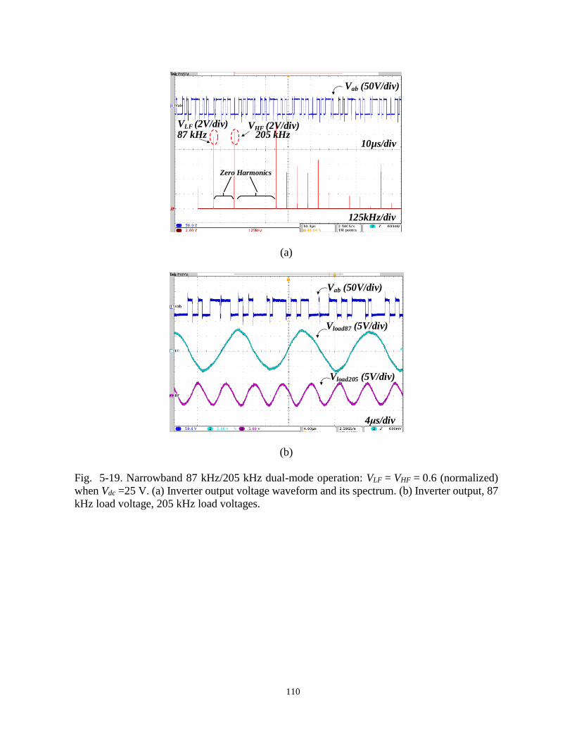
110
Vab (50V/div)
10µs/div
VHF (2V/div)VLF (2V/div)
125kHz/div
87 kHz 205 kHz
Zero Harmonics
(a)
Vab (50V/div)
Vload87 (5V/div)
Vload205 (5V/div)
4μs/div
(b)
Fig. 5-19. Narrowband 87 kHz/205 kHz dual-mode operation: VLF = VHF = 0.6 (normalized)
when Vdc =25 V. (a) Inverter output voltage waveform and its spectrum. (b) Inverter output, 87
kHz load voltage, 205 kHz load voltages.
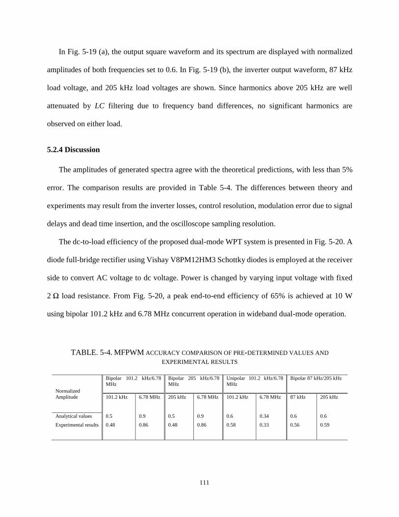
111
In Fig. 5-19 (a), the output square waveform and its spectrum are displayed with normalized
amplitudes of both frequencies set to 0.6. In Fig. 5-19 (b), the inverter output waveform, 87 kHz
load voltage, and 205 kHz load voltages are shown. Since harmonics above 205 kHz are well
attenuated by LC filtering due to frequency band differences, no significant harmonics are
observed on either load.
5.2.4 Discussion
The amplitudes of generated spectra agree with the theoretical predictions, with less than 5%
error. The comparison results are provided in Table 5-4. The differences between theory and
experiments may result from the inverter losses, control resolution, modulation error due to signal
delays and dead time insertion, and the oscilloscope sampling resolution.
The dc-to-load efficiency of the proposed dual-mode WPT system is presented in Fig. 5-20. A
diode full-bridge rectifier using Vishay V8PM12HM3 Schottky diodes is employed at the receiver
side to convert AC voltage to dc voltage. Power is changed by varying input voltage with fixed
2 Ω load resistance. From Fig. 5-20, a peak end-to-end efficiency of 65% is achieved at 10 W
using bipolar 101.2 kHz and 6.78 MHz concurrent operation in wideband dual-mode operation.
TABLE. 5-4. MFPWM ACCURACY COMPARISON OF PRE-DETERMINED VALUES AND
EXPERIMENTAL RESULTS
Normalized
Amplitude
Bipolar 101.2 kHz/6.78
MHz
Bipolar 205 kHz/6.78
MHz
Unipolar 101.2 kHz/6.78
MHz
Bipolar 87 kHz/205 kHz
101.2 kHz 6.78 MHz 205 kHz 6.78 MHz 101.2 kHz 6.78 MHz 87 kHz 205 kHz
Analytical values 0.5 0.9 0.5 0.9 0.6 0.34 0.6 0.6
Experimental results 0.48 0.86 0.48 0.86 0.58 0.33 0.56 0.59
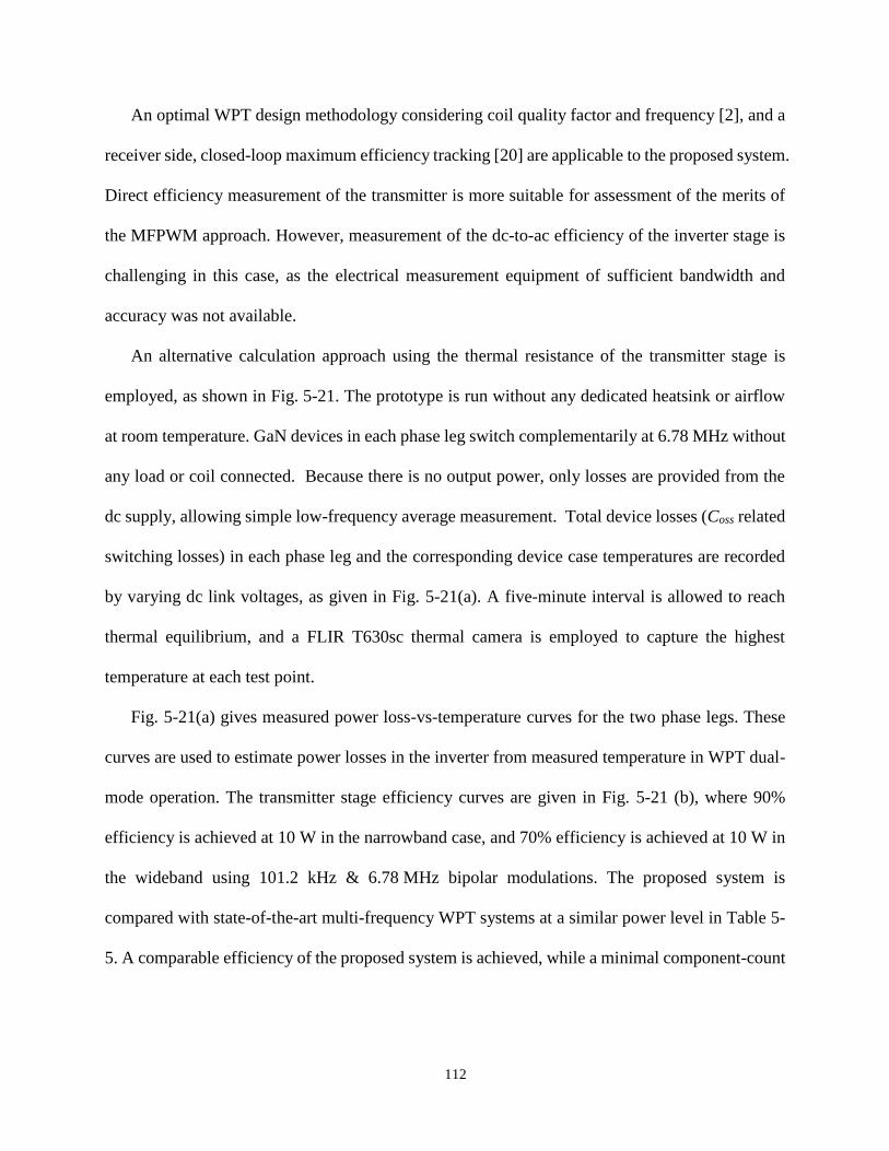
112
An optimal WPT design methodology considering coil quality factor and frequency [2], and a
receiver side, closed-loop maximum efficiency tracking [20] are applicable to the proposed system.
Direct efficiency measurement of the transmitter is more suitable for assessment of the merits of
the MFPWM approach. However, measurement of the dc-to-ac efficiency of the inverter stage is
challenging in this case, as the electrical measurement equipment of sufficient bandwidth and
accuracy was not available.
An alternative calculation approach using the thermal resistance of the transmitter stage is
employed, as shown in Fig. 5-21. The prototype is run without any dedicated heatsink or airflow
at room temperature. GaN devices in each phase leg switch complementarily at 6.78 MHz without
any load or coil connected. Because there is no output power, only losses are provided from the
dc supply, allowing simple low-frequency average measurement. Total device losses (Coss related
switching losses) in each phase leg and the corresponding device case temperatures are recorded
by varying dc link voltages, as given in Fig. 5-21(a). A five-minute interval is allowed to reach
thermal equilibrium, and a FLIR T630sc thermal camera is employed to capture the highest
temperature at each test point.
Fig. 5-21(a) gives measured power loss-vs-temperature curves for the two phase legs. These
curves are used to estimate power losses in the inverter from measured temperature in WPT dual-
mode operation. The transmitter stage efficiency curves are given in Fig. 5-21 (b), where 90%
efficiency is achieved at 10 W in the narrowband case, and 70% efficiency is achieved at 10 W in
the wideband using 101.2 kHz & 6.78 MHz bipolar modulations. The proposed system is
compared with state-of-the-art multi-frequency WPT systems at a similar power level in Table 5-
5. A comparable efficiency of the proposed system is achieved, while a minimal component-count
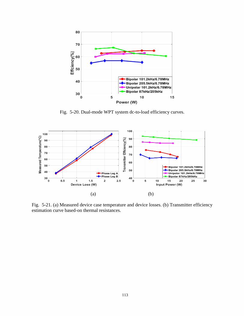
113
Fig. 5-20. Dual-mode WPT system dc-to-load efficiency curves.
(a) (b)
Fig. 5-21. (a) Measured device case temperature and device losses. (b) Transmitter efficiency
estimation curve based-on thermal resistances.
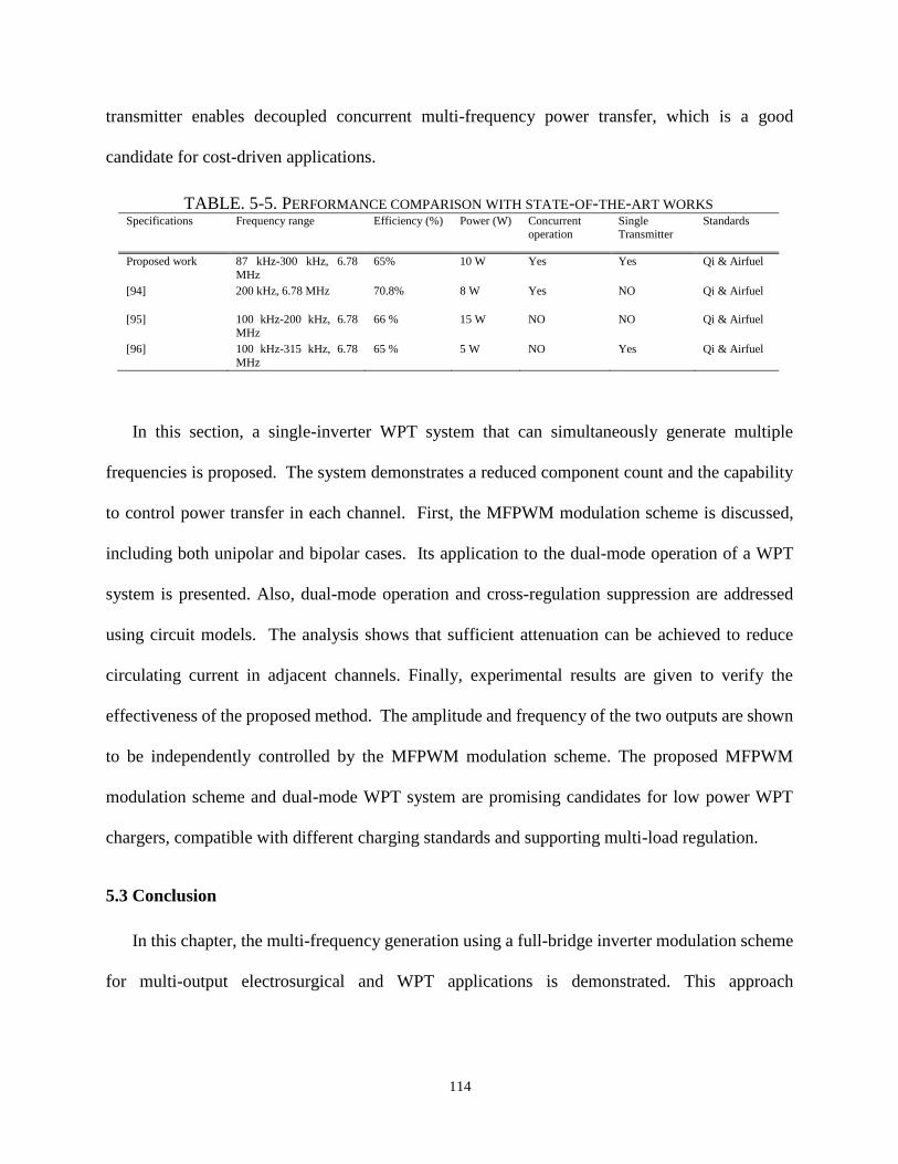
114
transmitter enables decoupled concurrent multi-frequency power transfer, which is a good
candidate for cost-driven applications.
In this section, a single-inverter WPT system that can simultaneously generate multiple
frequencies is proposed. The system demonstrates a reduced component count and the capability
to control power transfer in each channel. First, the MFPWM modulation scheme is discussed,
including both unipolar and bipolar cases. Its application to the dual-mode operation of a WPT
system is presented. Also, dual-mode operation and cross-regulation suppression are addressed
using circuit models. The analysis shows that sufficient attenuation can be achieved to reduce
circulating current in adjacent channels. Finally, experimental results are given to verify the
effectiveness of the proposed method. The amplitude and frequency of the two outputs are shown
to be independently controlled by the MFPWM modulation scheme. The proposed MFPWM
modulation scheme and dual-mode WPT system are promising candidates for low power WPT
chargers, compatible with different charging standards and supporting multi-load regulation.
5.3 Conclusion
In this chapter, the multi-frequency generation using a full-bridge inverter modulation scheme
for multi-output electrosurgical and WPT applications is demonstrated. This approach
TABLE. 5-5. PERFORMANCE COMPARISON WITH STATE-OF-THE-ART WORKS Specifications Frequency range Efficiency (%) Power (W) Concurrent
operation Single Transmitter
Standards
Proposed work 87 kHz-300 kHz, 6.78
MHz
65% 10 W Yes Yes Qi & Airfuel
[94] 200 kHz, 6.78 MHz 70.8% 8 W Yes NO Qi & Airfuel
[95] 100 kHz-200 kHz, 6.78
MHz
66 % 15 W NO NO Qi & Airfuel
[96] 100 kHz-315 kHz, 6.78
MHz
65 % 5 W NO Yes Qi & Airfuel
115
demonstrates a reduced component count and the capability to regulate output power at different
frequencies. In addition, the undesired low-order harmonics are eliminated from the modulation.
One valuable application of this technology is combining US and RF surgical power supplies
to enable improved performance and simultaneous usage. Three modulation schemes, unipolar,
bipolar and phase-shift MFPWM, are investigated. The experimental results from a 50W inverter
confirm the effectiveness of the proposed modulation methods, enabling the inverter to generate
two simultaneous high-frequency AC outputs with flexible power control.
For the WPT application, the MFPWM modulation scheme with an extensive frequency
controllable range is employed. The application of the MFPWM to a wideband and a narrowband
dual-mode operation of the WPT transmitter are presented, compatible with Qi and Airfuel
standards. Also, the dual-mode operation and the cross-regulation suppression are addressed using
circuit models. The analysis shows that sufficient attenuation can be achieved to reduce circulating
current loss in non-targeting channels. Finally, experimental results are given to verify the
effectiveness of the proposed method. The amplitude and frequency of the two outputs are shown
to be controlled by the MFPWM modulation scheme. The proposed MFPWM modulation scheme
and dual-mode WPT system are promising candidates for low power WPT chargers, compatible
with different charging standards and supporting multi-load regulation.
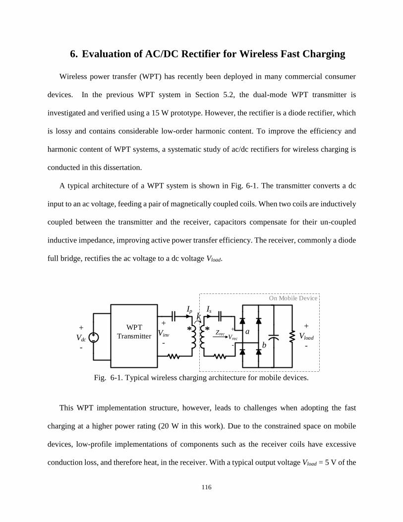
116
6. Evaluation of AC/DC Rectifier for Wireless Fast Charging
Wireless power transfer (WPT) has recently been deployed in many commercial consumer
devices. In the previous WPT system in Section 5.2, the dual-mode WPT transmitter is
investigated and verified using a 15 W prototype. However, the rectifier is a diode rectifier, which
is lossy and contains considerable low-order harmonic content. To improve the efficiency and
harmonic content of WPT systems, a systematic study of ac/dc rectifiers for wireless charging is
conducted in this dissertation.
A typical architecture of a WPT system is shown in Fig. 6-1. The transmitter converts a dc
input to an ac voltage, feeding a pair of magnetically coupled coils. When two coils are inductively
coupled between the transmitter and the receiver, capacitors compensate for their un-coupled
inductive impedance, improving active power transfer efficiency. The receiver, commonly a diode
full bridge, rectifies the ac voltage to a dc voltage Vload.
This WPT implementation structure, however, leads to challenges when adopting the fast
charging at a higher power rating (20 W in this work). Due to the constrained space on mobile
devices, low-profile implementations of components such as the receiver coils have excessive
conduction loss, and therefore heat, in the receiver. With a typical output voltage Vload = 5 V of the
* *
kWPT
Transmitter
On Mobile Device
+
Vload
-
Ip Is
Zrec a
b
+
Vrec
-
+
Vdc
-
+
Vinv
-
Fig. 6-1. Typical wireless charging architecture for mobile devices.
117
diode rectifier in Fig. 6-1, the diode and receiver coil will conduct a sinusoidal current with an
amplitude greater than 4 A when delivering 20 W. For a standard commercial receiver coil with Q
= 120 and L = 20 µH, this will result in 2.5 W of conduction loss on the coil, and a roughly equal
loss due to diode conduction, degrading efficiency and potentially resulting in overheating of the
mobile device.
In this chapter, four potential candidates for the circuit implementation of the wireless fast
charging receiver are assessed. The goals include: 1) to verify the feasibility of each candidate, 2)
to compare the loss, the total harmonic distortion (THD) of the current and the size of each
candidate, and 3) to select a circuit topology for a wireless fast charging receiver of consumer
electronics.
6.1 WPT Receiver: Candidate Topology Review
A WPT receiver converts the ac voltage, Vrec, from the resonant tank to the dc voltage for
battery charging, Vload, as shown in Fig. 6-1. The passive component parameters and device
parameters are given in Table 6-1. The receiving coil, compensation network, and rectifier are
integrated into the mobile device. This results in three design constraints for the system 1) high
power density and low-profile components are required due to space constraints; 2) high ac-dc
conversion efficiency is required due to fast charging speed power levels and limited heat
dissipation capability, and 3) the system must generate minimal harmonic content to meet EMI
and WPT standards and prevent potential interference for sensitive electronics. These constraints
limit the feasible design options for the system, as small and low-profile magnetics and WPT coils
are often prohibitively lossy.
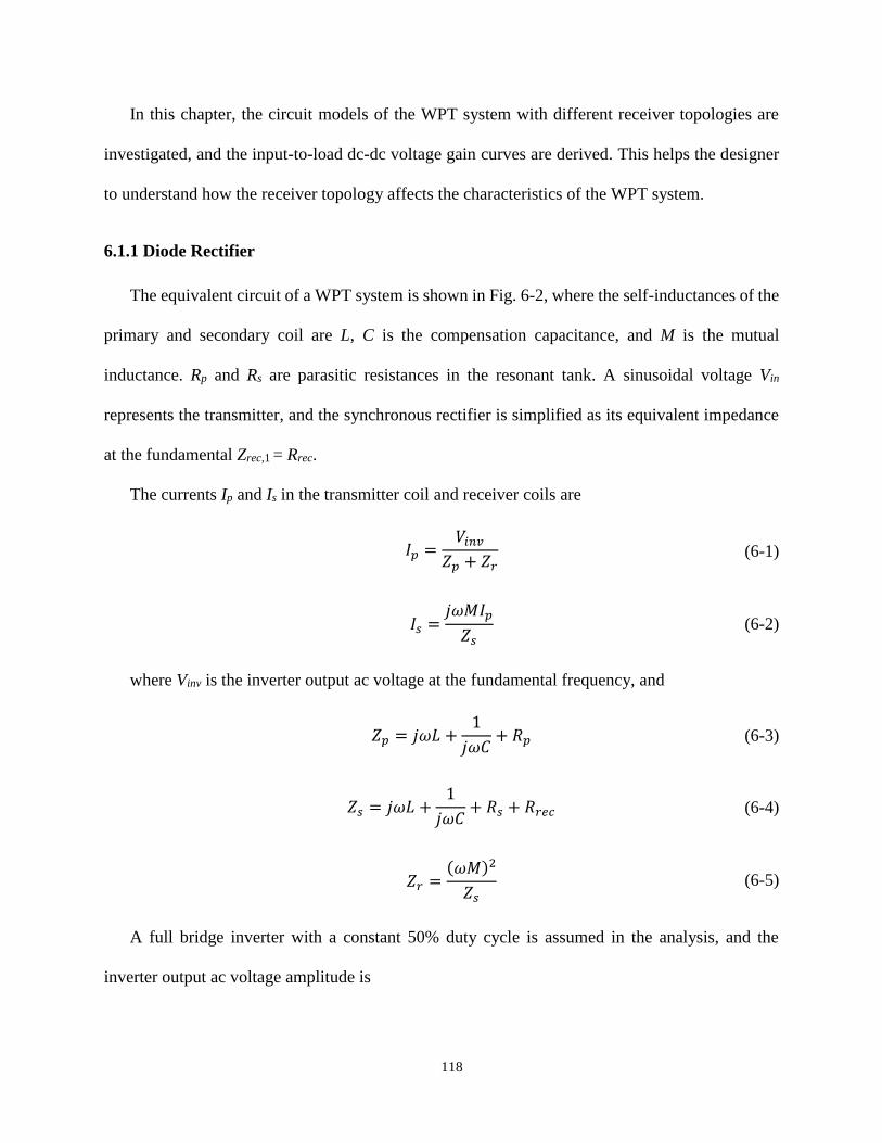
118
In this chapter, the circuit models of the WPT system with different receiver topologies are
investigated, and the input-to-load dc-dc voltage gain curves are derived. This helps the designer
to understand how the receiver topology affects the characteristics of the WPT system.
6.1.1 Diode Rectifier
The equivalent circuit of a WPT system is shown in Fig. 6-2, where the self-inductances of the
primary and secondary coil are L, C is the compensation capacitance, and M is the mutual
inductance. Rp and Rs are parasitic resistances in the resonant tank. A sinusoidal voltage Vin
represents the transmitter, and the synchronous rectifier is simplified as its equivalent impedance
at the fundamental Zrec,1 = Rrec.
The currents Ip and Is in the transmitter coil and receiver coils are
𝐼𝑝 =𝑉𝑖𝑛𝑣
𝑍𝑝 + 𝑍𝑟 (6-1)
𝐼𝑠 =𝑗𝜔𝑀𝐼𝑝
𝑍𝑠 (6-2)
where Vinv is the inverter output ac voltage at the fundamental frequency, and
𝑍𝑝 = 𝑗𝜔𝐿 +1
𝑗𝜔𝐶+ 𝑅𝑝 (6-3)
𝑍𝑠 = 𝑗𝜔𝐿 +1
𝑗𝜔𝐶+ 𝑅𝑠 + 𝑅𝑟𝑒𝑐 (6-4)
𝑍𝑟 =(𝜔𝑀)2
𝑍𝑠 (6-5)
A full bridge inverter with a constant 50% duty cycle is assumed in the analysis, and the
inverter output ac voltage amplitude is
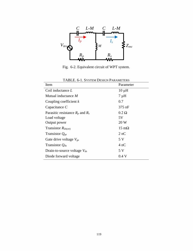
119
Vinv
C L-M L-MC
M Zrec
Ip Is
Rp Rs
Fig. 6-2. Equivalent circuit of WPT system.
TABLE. 6-1. SYSTEM DESIGN PARAMETERS
Item Parameter
Coil inductance L 10 µH
Mutual inductance M 7 µH
Coupling coefficient k 0.7
Capacitance C 375 nF
Parasitic resistance Rp and Rs 0.2 Ω
Load voltage 5V
Output power 20 W
Transistor Rds(on) 15 mΩ
Transistor Qgs 2 nC
Gate drive voltage Vgs 5 V
Transistor Qds 4 nC
Drain-to-source voltage Vds 5 V
Diode forward voltage 0.4 V
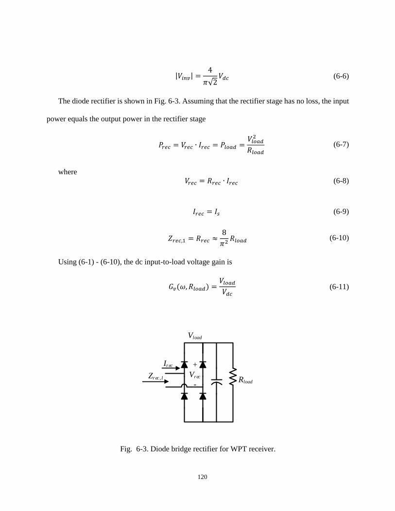
120
|𝑉𝑖𝑛𝑣| =4
𝜋√2𝑉𝑑𝑐 (6-6)
The diode rectifier is shown in Fig. 6-3. Assuming that the rectifier stage has no loss, the input
power equals the output power in the rectifier stage
𝑃𝑟𝑒𝑐 = 𝑉𝑟𝑒𝑐 ∙ 𝐼𝑟𝑒𝑐 = 𝑃𝑙𝑜𝑎𝑑 =𝑉𝑙𝑜𝑎𝑑
2
𝑅𝑙𝑜𝑎𝑑 (6-7)
where
𝑉𝑟𝑒𝑐 = 𝑅𝑟𝑒𝑐 ∙ 𝐼𝑟𝑒𝑐 (6-8)
𝐼𝑟𝑒𝑐 = 𝐼𝑠 (6-9)
𝑍𝑟𝑒𝑐,1 = 𝑅𝑟𝑒𝑐 ≈8
𝜋2𝑅𝑙𝑜𝑎𝑑 (6-10)
Using (6-1) - (6-10), the dc input-to-load voltage gain is
𝐺𝑣(𝜔, 𝑅𝑙𝑜𝑎𝑑) =𝑉𝑙𝑜𝑎𝑑
𝑉𝑑𝑐 (6-11)
Vload
RloadZrec ,1
+
Vrec
-
Irec
Fig. 6-3. Diode bridge rectifier for WPT receiver.
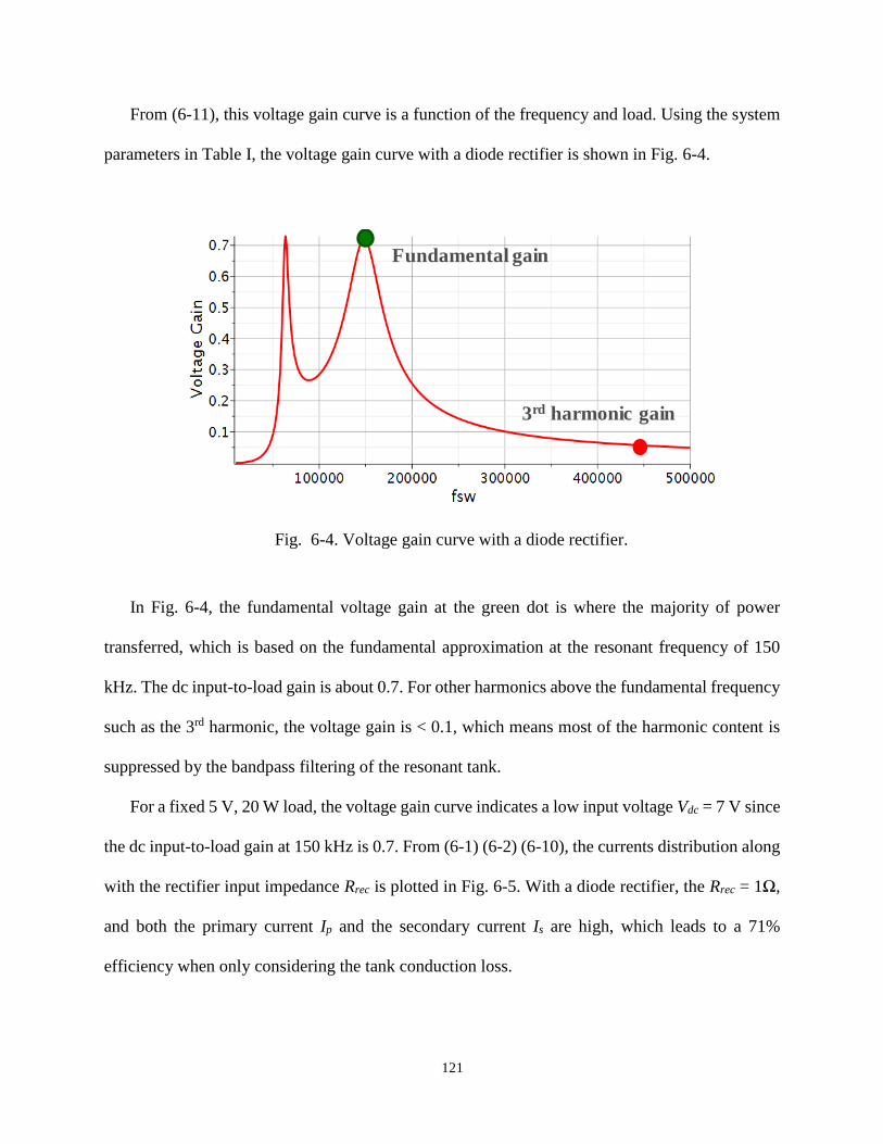
121
From (6-11), this voltage gain curve is a function of the frequency and load. Using the system
parameters in Table I, the voltage gain curve with a diode rectifier is shown in Fig. 6-4.
In Fig. 6-4, the fundamental voltage gain at the green dot is where the majority of power
transferred, which is based on the fundamental approximation at the resonant frequency of 150
kHz. The dc input-to-load gain is about 0.7. For other harmonics above the fundamental frequency
such as the 3rd harmonic, the voltage gain is < 0.1, which means most of the harmonic content is
suppressed by the bandpass filtering of the resonant tank.
For a fixed 5 V, 20 W load, the voltage gain curve indicates a low input voltage Vdc = 7 V since
the dc input-to-load gain at 150 kHz is 0.7. From (6-1) (6-2) (6-10), the currents distribution along
with the rectifier input impedance Rrec is plotted in Fig. 6-5. With a diode rectifier, the Rrec = 1Ω,
and both the primary current Ip and the secondary current Is are high, which leads to a 71%
efficiency when only considering the tank conduction loss.
Fig. 6-4. Voltage gain curve with a diode rectifier.
Fundamental gain
3rd harmonic gain
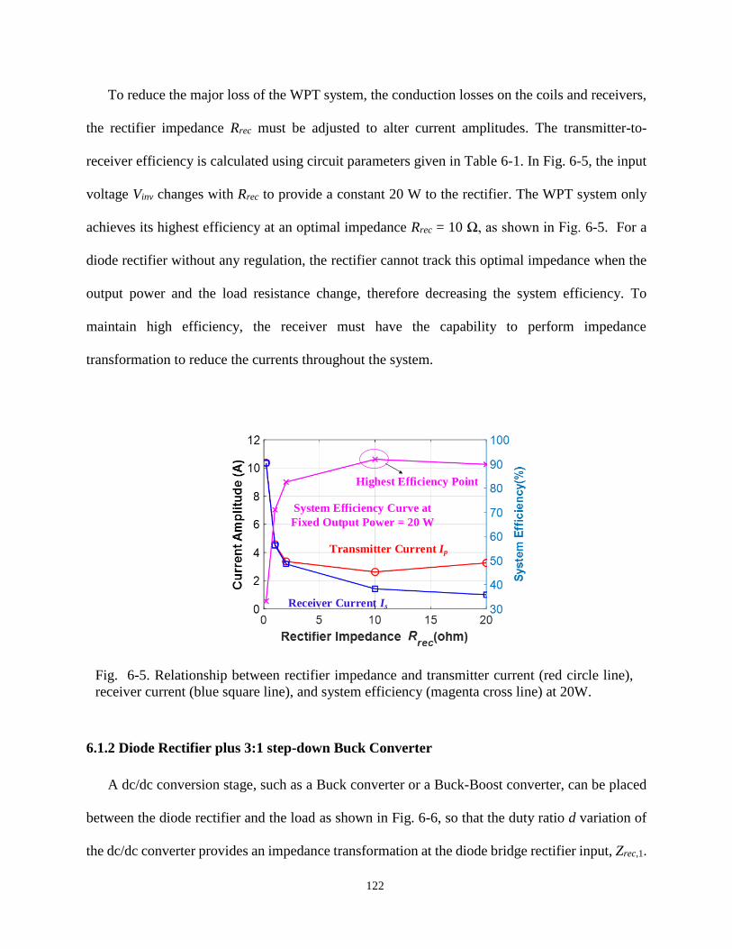
122
To reduce the major loss of the WPT system, the conduction losses on the coils and receivers,
the rectifier impedance Rrec must be adjusted to alter current amplitudes. The transmitter-to-
receiver efficiency is calculated using circuit parameters given in Table 6-1. In Fig. 6-5, the input
voltage Vinv changes with Rrec to provide a constant 20 W to the rectifier. The WPT system only
achieves its highest efficiency at an optimal impedance Rrec = 10 Ω, as shown in Fig. 6-5. For a
diode rectifier without any regulation, the rectifier cannot track this optimal impedance when the
output power and the load resistance change, therefore decreasing the system efficiency. To
maintain high efficiency, the receiver must have the capability to perform impedance
transformation to reduce the currents throughout the system.
6.1.2 Diode Rectifier plus 3:1 step-down Buck Converter
A dc/dc conversion stage, such as a Buck converter or a Buck-Boost converter, can be placed
between the diode rectifier and the load as shown in Fig. 6-6, so that the duty ratio d variation of
the dc/dc converter provides an impedance transformation at the diode bridge rectifier input, Zrec,1.
Receiver Current Is
Transmitter Current Ip
System Efficiency Curve at
Fixed Output Power = 20 W
Highest Efficiency Point
Fig. 6-5. Relationship between rectifier impedance and transmitter current (red circle line),
receiver current (blue square line), and system efficiency (magenta cross line) at 20W.
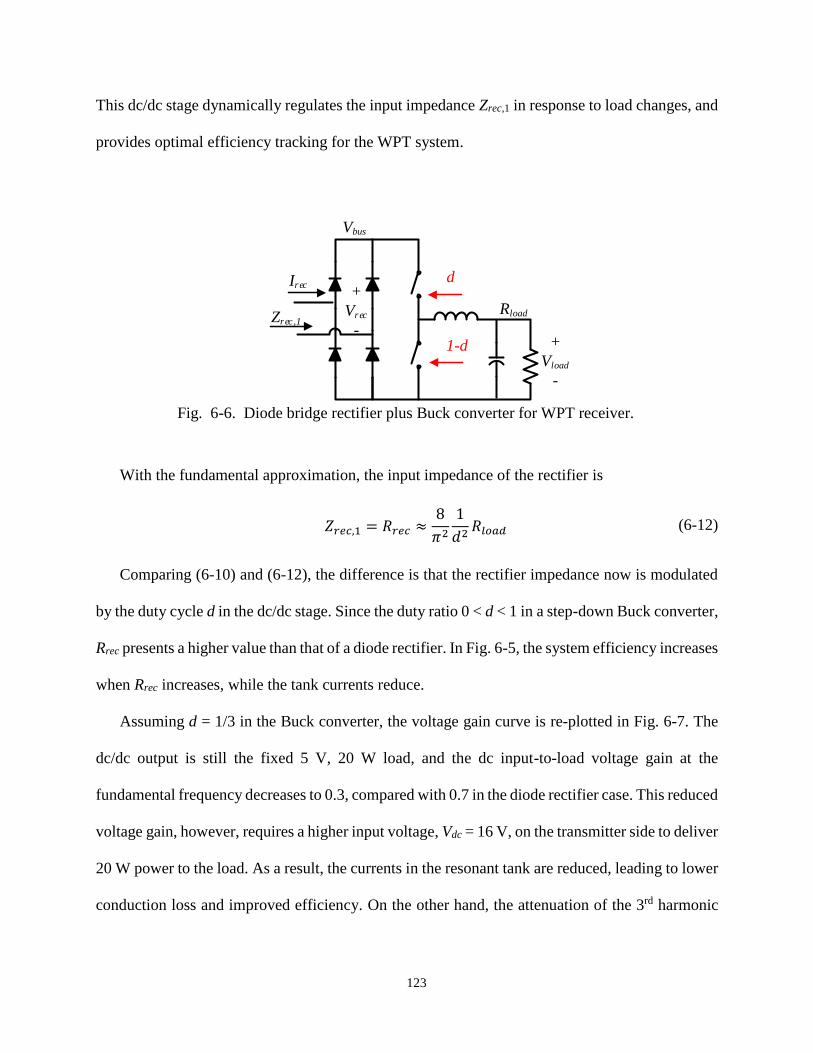
123
This dc/dc stage dynamically regulates the input impedance Zrec,1 in response to load changes, and
provides optimal efficiency tracking for the WPT system.
With the fundamental approximation, the input impedance of the rectifier is
𝑍𝑟𝑒𝑐,1 = 𝑅𝑟𝑒𝑐 ≈8
𝜋2
1
𝑑2𝑅𝑙𝑜𝑎𝑑 (6-12)
Comparing (6-10) and (6-12), the difference is that the rectifier impedance now is modulated
by the duty cycle d in the dc/dc stage. Since the duty ratio 0 < d < 1 in a step-down Buck converter,
Rrec presents a higher value than that of a diode rectifier. In Fig. 6-5, the system efficiency increases
when Rrec increases, while the tank currents reduce.
Assuming d = 1/3 in the Buck converter, the voltage gain curve is re-plotted in Fig. 6-7. The
dc/dc output is still the fixed 5 V, 20 W load, and the dc input-to-load voltage gain at the
fundamental frequency decreases to 0.3, compared with 0.7 in the diode rectifier case. This reduced
voltage gain, however, requires a higher input voltage, Vdc = 16 V, on the transmitter side to deliver
20 W power to the load. As a result, the currents in the resonant tank are reduced, leading to lower
conduction loss and improved efficiency. On the other hand, the attenuation of the 3rd harmonic
Fig. 6-6. Diode bridge rectifier plus Buck converter for WPT receiver.
Rload
d
1-d
+
Vrec
-
Irec
+
Vload
-
Vbus
Zrec ,1

124
increases from 0.1 in the diode rectifier case to 0.2 in this case. The increased rectifier impedance
weakens the band-pass filtering of the resonant tank, leaking more harmonic content.
Fig. 6-8 shows the primary and secondary current stresses as the rectifier impedance is adjusted,
using the parameters in Table 6-1. Both transmitter and receiver currents reduce with larger
rectifier input impedance for 0.4 < d < 1. If conduction losses in the coils and receiver dominate
the total system loss, which is true in many applications, increasing the rectifier impedance will
benefit the overall system efficiency. Moreover, the system maximum efficiency depends on both
transmitter and receiver loss, and the efficiency curve has a non-monotonic relationship with duty
cycle d. Control strategies such as perturbation and observe (P&O) or systematic efficiency
optimization are required to reach a maximum efficiency point. The optimal rectifier impedance
is Rrec = 10 Ω in this case, and this impedance is achieved by adjusting the duty ratio to d = 1/3 in
the dc/dc converter.
However, the bulky magnetic components introduce a barrier to integration for mobile devices.
Moreover, the input impedance of a Buck converter follows Zrec,1∝1/d2, where d is the duty ratio.
The higher impedance it offers to the rectifier stage, the higher voltage stress it will cause on the
inductor in the dc/dc stage, and therefore it may lead to larger inductor volume and high core loss,
which could counteract the reduction in conduction loss.
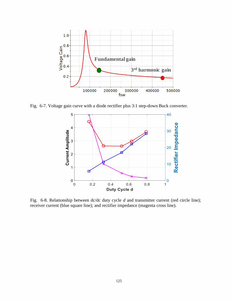
125
Fig. 6-7. Voltage gain curve with a diode rectifier plus 3:1 step-down Buck converter.
Fig. 6-8. Relationship between dc/dc duty cycle d and transmitter current (red circle line);
receiver current (blue square line); and rectifier impedance (magenta cross line).
Fundamental gain
3rd harmonic gain
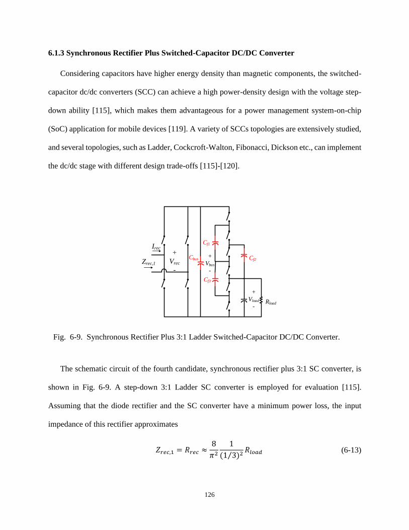
126
6.1.3 Synchronous Rectifier Plus Switched-Capacitor DC/DC Converter
Considering capacitors have higher energy density than magnetic components, the switched-
capacitor dc/dc converters (SCC) can achieve a high power-density design with the voltage step-
down ability [115], which makes them advantageous for a power management system-on-chip
(SoC) application for mobile devices [119]. A variety of SCCs topologies are extensively studied,
and several topologies, such as Ladder, Cockcroft-Walton, Fibonacci, Dickson etc., can implement
the dc/dc stage with different design trade-offs [115]-[120].
The schematic circuit of the fourth candidate, synchronous rectifier plus 3:1 SC converter, is
shown in Fig. 6-9. A step-down 3:1 Ladder SC converter is employed for evaluation [115].
Assuming that the diode rectifier and the SC converter have a minimum power loss, the input
impedance of this rectifier approximates
𝑍𝑟𝑒𝑐,1 = 𝑅𝑟𝑒𝑐 ≈8
𝜋2
1
(1 3⁄ )2𝑅𝑙𝑜𝑎𝑑 (6-13)
+
Vrec
-
Irec
Zrec,1
Rload
+
Vload
-
+
Vbus
-
Cf1
Cf2
Cf3
Cbus
Fig. 6-9. Synchronous Rectifier Plus 3:1 Ladder Switched-Capacitor DC/DC Converter.
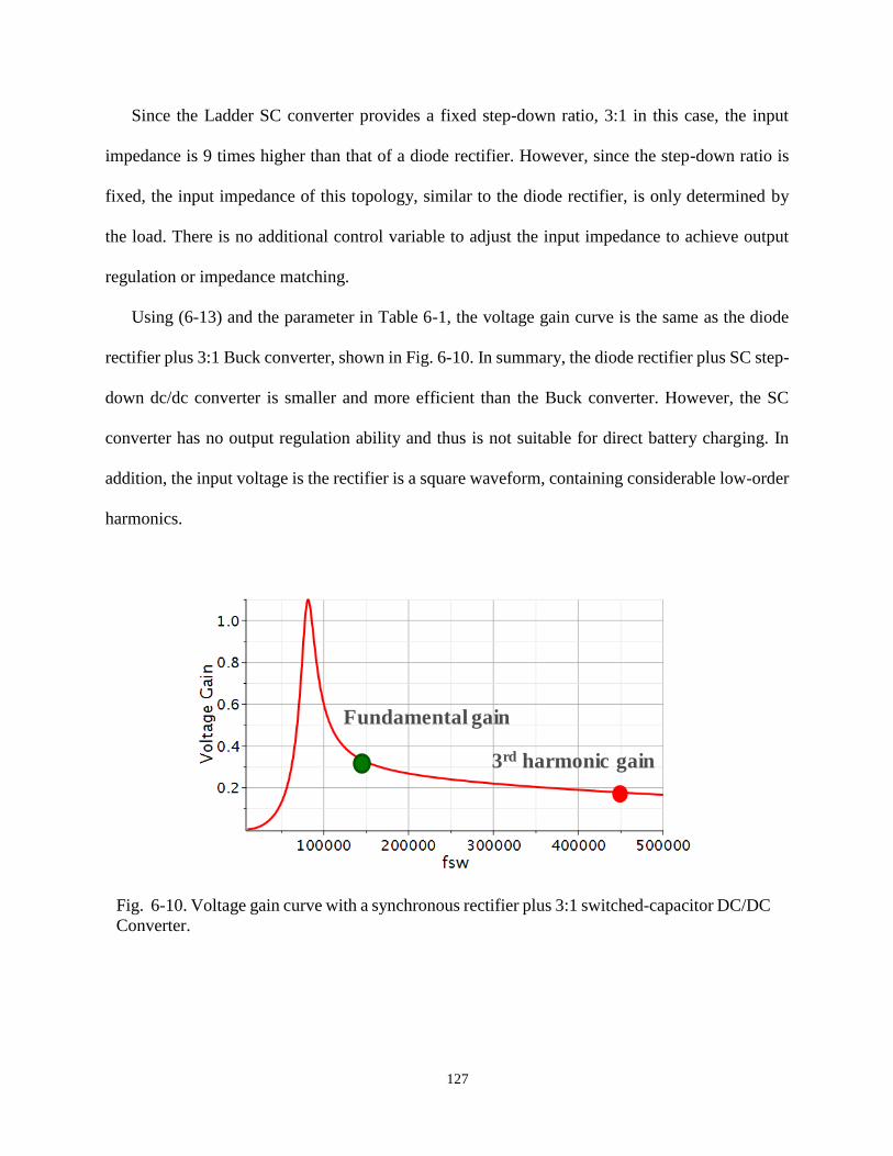
127
Since the Ladder SC converter provides a fixed step-down ratio, 3:1 in this case, the input
impedance is 9 times higher than that of a diode rectifier. However, since the step-down ratio is
fixed, the input impedance of this topology, similar to the diode rectifier, is only determined by
the load. There is no additional control variable to adjust the input impedance to achieve output
regulation or impedance matching.
Using (6-13) and the parameter in Table 6-1, the voltage gain curve is the same as the diode
rectifier plus 3:1 Buck converter, shown in Fig. 6-10. In summary, the diode rectifier plus SC step-
down dc/dc converter is smaller and more efficient than the Buck converter. However, the SC
converter has no output regulation ability and thus is not suitable for direct battery charging. In
addition, the input voltage is the rectifier is a square waveform, containing considerable low-order
harmonics.
Fig. 6-10. Voltage gain curve with a synchronous rectifier plus 3:1 switched-capacitor DC/DC
Converter.
Fundamental gain
3rd harmonic gain
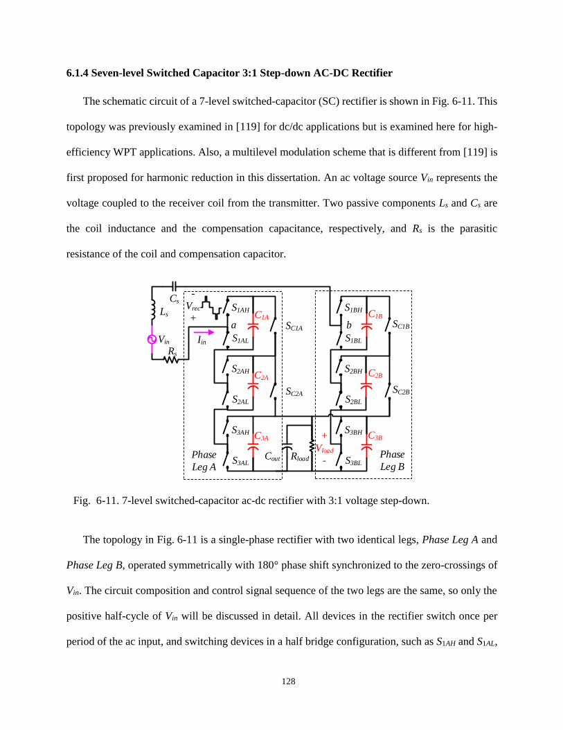
128
6.1.4 Seven-level Switched Capacitor 3:1 Step-down AC-DC Rectifier
The schematic circuit of a 7-level switched-capacitor (SC) rectifier is shown in Fig. 6-11. This
topology was previously examined in [119] for dc/dc applications but is examined here for high-
efficiency WPT applications. Also, a multilevel modulation scheme that is different from [119] is
first proposed for harmonic reduction in this dissertation. An ac voltage source Vin represents the
voltage coupled to the receiver coil from the transmitter. Two passive components Ls and Cs are
the coil inductance and the compensation capacitance, respectively, and Rs is the parasitic
resistance of the coil and compensation capacitor.
The topology in Fig. 6-11 is a single-phase rectifier with two identical legs, Phase Leg A and
Phase Leg B, operated symmetrically with 180° phase shift synchronized to the zero-crossings of
Vin. The circuit composition and control signal sequence of the two legs are the same, so only the
positive half-cycle of Vin will be discussed in detail. All devices in the rectifier switch once per
period of the ac input, and switching devices in a half bridge configuration, such as S1AH and S1AL,
Ls
Cs
Iin
Rs
-
Vrec
+
Vin
Rload
C1A
C2A
C3A
C1B
C2B
C3B
Cout
+
Vload
-
SC1Aa b
Phase
Leg A
Phase
Leg B
S1AH
SC2A
SC1B
SC2B
S1AL
S2AH
S2AL
S3AH
S3AL
S1BH
S1BL
S2BH
S2BL
S3BH
S3BL
Fig. 6-11. 7-level switched-capacitor ac-dc rectifier with 3:1 voltage step-down.
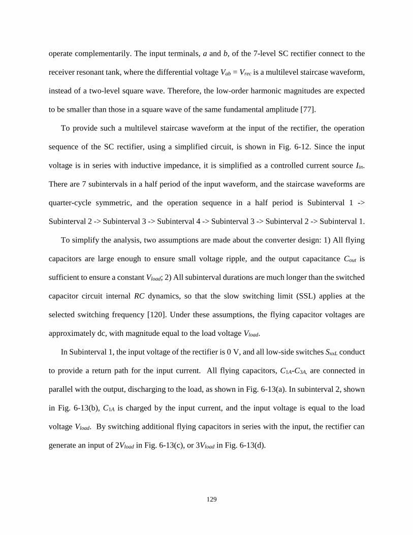
129
operate complementarily. The input terminals, a and b, of the 7-level SC rectifier connect to the
receiver resonant tank, where the differential voltage Vab = Vrec is a multilevel staircase waveform,
instead of a two-level square wave. Therefore, the low-order harmonic magnitudes are expected
to be smaller than those in a square wave of the same fundamental amplitude [77].
To provide such a multilevel staircase waveform at the input of the rectifier, the operation
sequence of the SC rectifier, using a simplified circuit, is shown in Fig. 6-12. Since the input
voltage is in series with inductive impedance, it is simplified as a controlled current source Iin.
There are 7 subintervals in a half period of the input waveform, and the staircase waveforms are
quarter-cycle symmetric, and the operation sequence in a half period is Subinterval 1 ->
Subinterval 2 -> Subinterval 3 -> Subinterval 4 -> Subinterval 3 -> Subinterval 2 -> Subinterval 1.
To simplify the analysis, two assumptions are made about the converter design: 1) All flying
capacitors are large enough to ensure small voltage ripple, and the output capacitance Cout is
sufficient to ensure a constant Vload; 2) All subinterval durations are much longer than the switched
capacitor circuit internal RC dynamics, so that the slow switching limit (SSL) applies at the
selected switching frequency [120]. Under these assumptions, the flying capacitor voltages are
approximately dc, with magnitude equal to the load voltage Vload.
In Subinterval 1, the input voltage of the rectifier is 0 V, and all low-side switches SxxL conduct
to provide a return path for the input current. All flying capacitors, C1A-C3A, are connected in
parallel with the output, discharging to the load, as shown in Fig. 6-13(a). In subinterval 2, shown
in Fig. 6-13(b), C1A is charged by the input current, and the input voltage is equal to the load
voltage Vload. By switching additional flying capacitors in series with the input, the rectifier can
generate an input of 2Vload in Fig. 6-13(c), or 3Vload in Fig. 6-13(d).
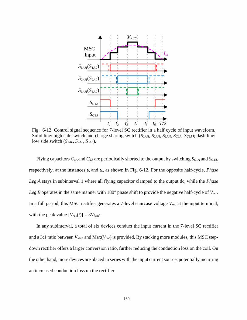
130
Flying capacitors C1A and C2A are periodically shorted to the output by switching SC1A and SC2A,
respectively, at the instances t5 and t6, as shown in Fig. 6-12. For the opposite half-cycle, Phase
Leg A stays in subinterval 1 where all flying capacitor clamped to the output dc, while the Phase
Leg B operates in the same manner with 180° phase shift to provide the negative half-cycle of Vrec.
In a full period, this MSC rectifier generates a 7-level staircase voltage Vrec at the input terminal,
with the peak value ⌈Vrec(t)⌉ = 3Vload.
In any subinterval, a total of six devices conduct the input current in the 7-level SC rectifier
and a 3:1 ratio between Vload and Max(Vrec) is provided. By stacking more modules, this MSC step-
down rectifier offers a larger conversion ratio, further reducing the conduction loss on the coil. On
the other hand, more devices are placed in series with the input current source, potentially incurring
an increased conduction loss on the rectifier.
MSC
Input
SC1A
Iin
VREC
T/2t1 t2 t3 t4 t5 t6
S1AH(S1AL)
SC2A
S2AH(S2AL)
S3AH(S3AL)
Fig. 6-12. Control signal sequence for 7-level SC rectifier in a half cycle of input waveform.
Solid line: high side switch and charge sharing switch (S1AH, S2AH, S3AH, SC1A, SC2A); dash line:
low side switch (S1AL, S2AL, S3AL).
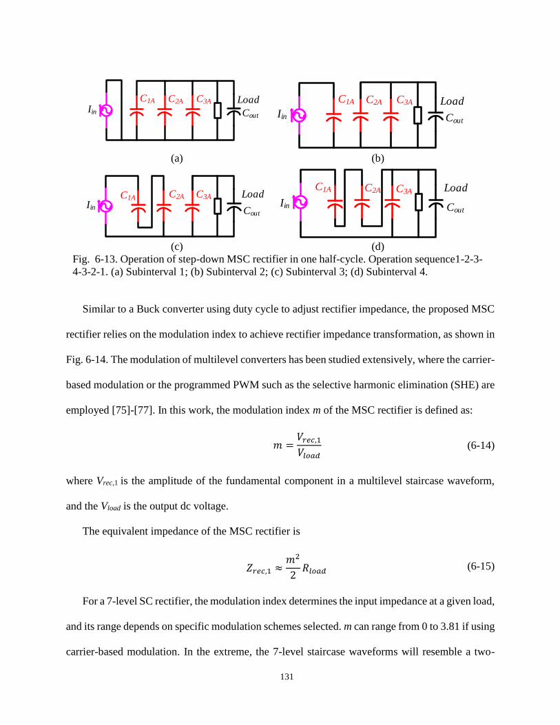
131
Similar to a Buck converter using duty cycle to adjust rectifier impedance, the proposed MSC
rectifier relies on the modulation index to achieve rectifier impedance transformation, as shown in
Fig. 6-14. The modulation of multilevel converters has been studied extensively, where the carrier-
based modulation or the programmed PWM such as the selective harmonic elimination (SHE) are
employed [75]-[77]. In this work, the modulation index m of the MSC rectifier is defined as:
𝑚 =𝑉𝑟𝑒𝑐,1
𝑉𝑙𝑜𝑎𝑑 (6-14)
where Vrec,1 is the amplitude of the fundamental component in a multilevel staircase waveform,
and the Vload is the output dc voltage.
The equivalent impedance of the MSC rectifier is
𝑍𝑟𝑒𝑐,1 ≈𝑚2
2𝑅𝑙𝑜𝑎𝑑 (6-15)
For a 7-level SC rectifier, the modulation index determines the input impedance at a given load,
and its range depends on specific modulation schemes selected. m can range from 0 to 3.81 if using
carrier-based modulation. In the extreme, the 7-level staircase waveforms will resemble a two-
C1A C2A C3A
Iin
Load
Cout
C1A C2A C3A
Iin
Load
Cout
(a) (b)
C1A C2A C3A
Iin
Load
Cout
C1A C2A C3A
Iin
Load
Cout
(c) (d)
Fig. 6-13. Operation of step-down MSC rectifier in one half-cycle. Operation sequence1-2-3-
4-3-2-1. (a) Subinterval 1; (b) Subinterval 2; (c) Subinterval 3; (d) Subinterval 4.
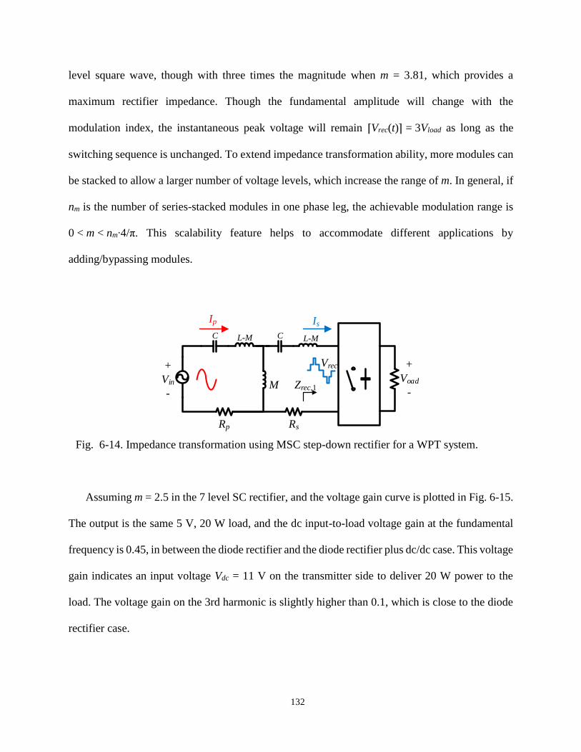
132
level square wave, though with three times the magnitude when m = 3.81, which provides a
maximum rectifier impedance. Though the fundamental amplitude will change with the
modulation index, the instantaneous peak voltage will remain ⌈Vrec(t)⌉ = 3Vload as long as the
switching sequence is unchanged. To extend impedance transformation ability, more modules can
be stacked to allow a larger number of voltage levels, which increase the range of m. In general, if
nm is the number of series-stacked modules in one phase leg, the achievable modulation range is
0 < m < nm∙4/π. This scalability feature helps to accommodate different applications by
adding/bypassing modules.
Assuming m = 2.5 in the 7 level SC rectifier, and the voltage gain curve is plotted in Fig. 6-15.
The output is the same 5 V, 20 W load, and the dc input-to-load voltage gain at the fundamental
frequency is 0.45, in between the diode rectifier and the diode rectifier plus dc/dc case. This voltage
gain indicates an input voltage Vdc = 11 V on the transmitter side to deliver 20 W power to the
load. The voltage gain on the 3rd harmonic is slightly higher than 0.1, which is close to the diode
rectifier case.
C L-M L-MC
M
Vrec+
Vin
-
+
Voad
-
Ip Is
Zrec,1
Rp Rs
Fig. 6-14. Impedance transformation using MSC step-down rectifier for a WPT system.
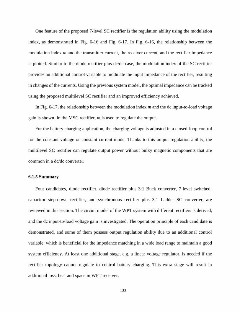
133
One feature of the proposed 7-level SC rectifier is the regulation ability using the modulation
index, as demonstrated in Fig. 6-16 and Fig. 6-17. In Fig. 6-16, the relationship between the
modulation index m and the transmitter current, the receiver current, and the rectifier impedance
is plotted. Similar to the diode rectifier plus dc/dc case, the modulation index of the SC rectifier
provides an additional control variable to modulate the input impedance of the rectifier, resulting
in changes of the currents. Using the previous system model, the optimal impedance can be tracked
using the proposed multilevel SC rectifier and an improved efficiency achieved.
In Fig. 6-17, the relationship between the modulation index m and the dc input-to-load voltage
gain is shown. In the MSC rectifier, m is used to regulate the output.
For the battery charging application, the charging voltage is adjusted in a closed-loop control
for the constant voltage or constant current mode. Thanks to this output regulation ability, the
multilevel SC rectifier can regulate output power without bulky magnetic components that are
common in a dc/dc converter.
6.1.5 Summary
Four candidates, diode rectifier, diode rectifier plus 3:1 Buck converter, 7-level switched-
capacitor step-down rectifier, and synchronous rectifier plus 3:1 Ladder SC converter, are
reviewed in this section. The circuit model of the WPT system with different rectifiers is derived,
and the dc input-to-load voltage gain is investigated. The operation principle of each candidate is
demonstrated, and some of them possess output regulation ability due to an additional control
variable, which is beneficial for the impedance matching in a wide load range to maintain a good
system efficiency. At least one additional stage, e.g. a linear voltage regulator, is needed if the
rectifier topology cannot regulate to control battery charging. This extra stage will result in
additional loss, heat and space in WPT receiver.
134
Fig. 6-15. Voltage gain curve with a 7-level step-down switched capacitor ac-dc rectifier, m =
2.5 and Rload = 1.25 Ω.
Fig. 6-16. Relationship between modulation index m and transmitter current (red circle line);
receiver current (blue square line); and rectifier impedance (magenta cross line).
Fig. 6-17. Relationship between modulation index m and the dc input-to-load voltage gain at
150 kHz, and given load Rload = 1.25 Ω.
Fundamental gain
3rd harmonic gain
Voltage gain
@m = 2.5

135
In Table 6-2, the four candidates are compared based on the previous discussion. In summary,
the diode rectifier will suffer a high conduction loss due to a high dc input-to-load voltage gain,
and a low-voltage, high-current configuration is inevitable to deliver 20W to a 5V output. For other
candidates, the voltage step-down ability of the rectifier achieves a high-voltage, low-current
configuration in the system to deliver the same amount of power to the load, resulting in an
increased input impedance of the rectifier. This is advantageous since the conduction loss
dominates the overall loss in wireless fast charging applications. In addition, two candidates, diode
rectifier plus 3:1 Buck converter and 7-level switched-capacitor step-down rectifier, have
adjustable input impedance, which enables output regulation and impedance matching for differing
loads.
On the other hand, the diode rectifier provides the highest attenuation on the low-order
harmonics from the dc input-to-load voltage gain curves, and this feature is advantageous to reduce
current THD and maintain a spectrum within the allowable band. The other candidates with voltage
step-down ability have less-effective attenuation of the harmonic content due to the reduced quality
factor of the resonant tank when increasing the rectifier impedance.
TABLE. 6-2. VOLTAGE GAIN AND REGULATION COMPARISON OF FOUR CANDIDATES
Candidate 1 Candidate 2 Candidate 3 Candidate 4
input-to-load gain 0.7 0.3 0.45 (m = 2.5) 0.3
3rd harmonic gain <0.1 0.2 0.1 0.2
Output regulation No Yes Yes No
*Candidate 1: Diode rectifier
*Candidate 2: diode rectifier plus 3:1 Buck converter
*Candidate 3: 7-level switched-capacitor step-down rectifier
*Candidate 4: synchronous rectifier plus 3:1 Ladder SC converter

136
6.2 Function Simulation and Loss Estimation
In this section, a simulation-based circuit verification is conducted to validate the four
candidates for wireless fast charging applications. A simulation platform of the complete
transmitter-to-receiver system is designed, and the simulated system parameters are displayed in
Table 6-1. The output is a 5V, 20W resistive load and the transmitter is simplified as a square-
wave voltage source to mimic a 50% duty output voltage.
Note that the simulation waveforms in the chapter are to demonstrate the main circuit behaviors
without considering practical issues, such as the detailed modeling of switching devices, dead time
and thermal changes. All switching devices in this simulation are ideal without output capacitance
and conduction resistance. All passives are ideal without parasitic parameters.
To compare system loss that is close to practical WPT system, transistor parameters and diode
parameter from selected commercial devices at given voltage/current rating, given in Table 6-1.
These devices are the state-of-the art products. The parasitic resistance of the resonant are extracted
from commercial WPT coils for mobile devices. The loss estimation of the complete WPT system
includes the switching and conduction loss of the semiconductor devices, and the conduction loss
of the resonant tank.
6.2.1 Diode Rectifier
The simulation results using a diode bridge rectifier are shown in Fig. 6-18. The schematic
circuit is given in Fig. 6-18 (a). The inverter voltage and current, receiver voltage and current are
shown as Vsource and Isource, Vrec and Irec, respectively in Fig. 6-18(b). In the strong coupling region,
the inverter voltage and the rectifier voltage, Vsource and Vrec, has near zero phase angle, and the
currents on both sides are close to pure sinusoids, as shown in Fig. 6-18(b). As predicted in Section
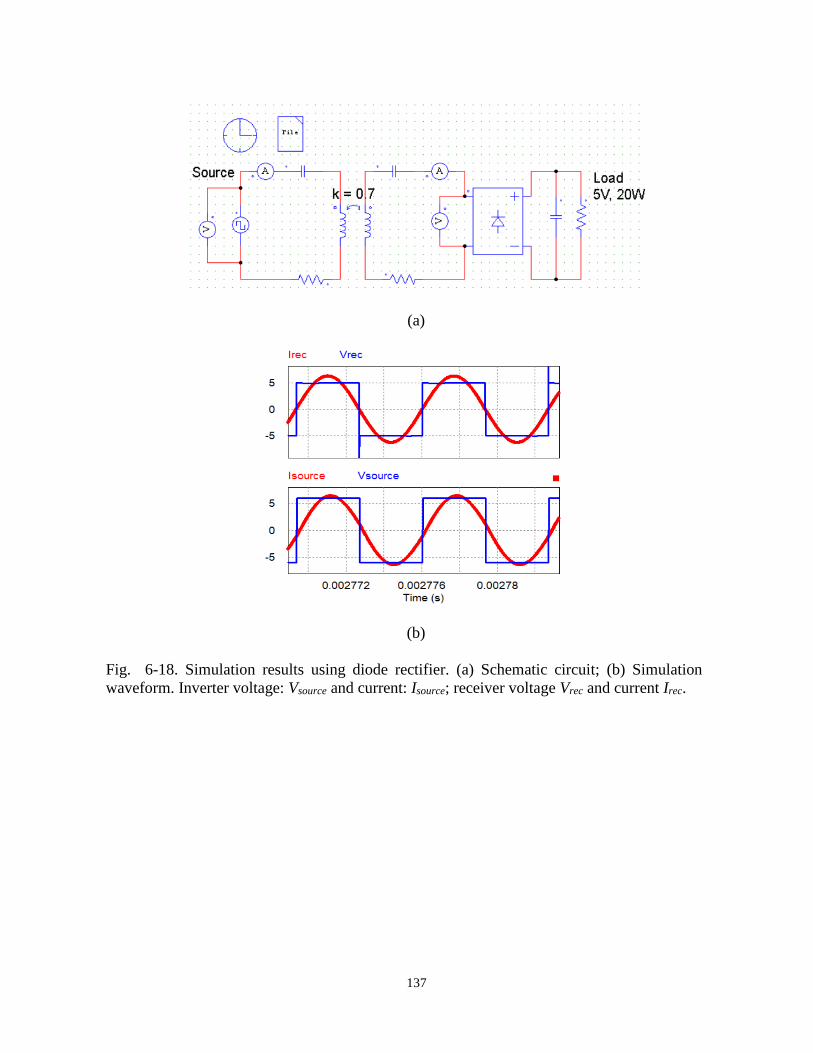
137
(a)
(b)
Fig. 6-18. Simulation results using diode rectifier. (a) Schematic circuit; (b) Simulation
waveform. Inverter voltage: Vsource and current: Isource; receiver voltage Vrec and current Irec.

138
6.1, the voltage amplitude is near 5V, and current amplitudes are over 5A, which leads to high
conduction loss.
The loss mechanisms of a WPT system using the diode rectifier are presented as follows.
Using the equations that describe the WPT circuit model (6-1) - (6-10), the voltages and the
currents in the WPT system are calculated, and those voltages and currents are used to calculate
the system losses. The MOSFETs and the diodes used in the loss calculation are examples, subject
to alternatives.
1) Conduction loss
The conduction loss consists of the loss from the inverter, the resonant tank, and the rectifier.
The inverter conduction loss is
𝑃𝑐𝑜𝑛𝑑_𝑖𝑛𝑣 = 2 ∙ 𝐼𝑝2 ∙ 𝑅𝑑𝑠 (6-16)
where Ip = 4.5A is the primary current rms value, and Rds = 16 mΩ is the conduction resistance of
the MOSFET of the inverter. The tank conduction loss is
𝑃𝑐𝑜𝑛𝑑_𝑡𝑎𝑛𝑘 = 𝐼𝑝2 ∙ 𝑅𝑝 + 𝐼𝑠
2 ∙ 𝑅𝑠 (6-17)
where Ip is the primary current rms value and Is = 4.45A is the secondary current rms value. RL
and RC are the series resistance of the coil and the compensation capacitor, and Rp = Rs = RL+Rc,
in Fig. 6-2.
The rectifier conduction loss is
𝑃𝑐𝑜𝑛𝑑_𝑟𝑒𝑐 = 2 ∙2
𝑇∫ 𝑉𝐹 ∙ 𝑖𝑠(𝑡)𝑑𝑡
𝑇/2
0
(6-18)
where is(t) is the rectifier input current; VF is the diode conduction voltage and T is the switching
period.
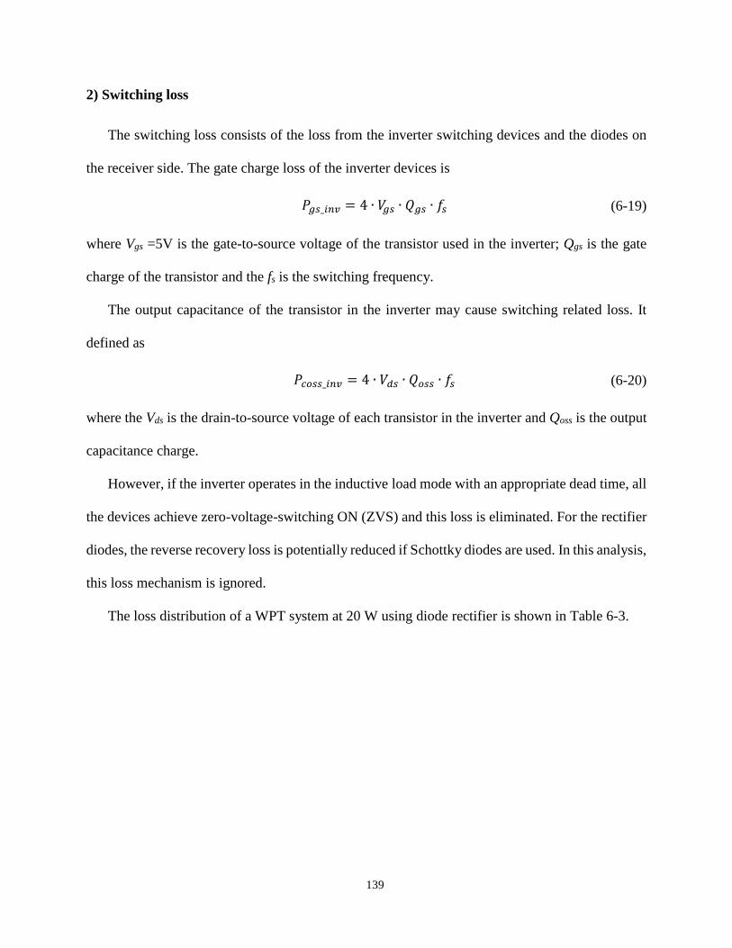
139
2) Switching loss
The switching loss consists of the loss from the inverter switching devices and the diodes on
the receiver side. The gate charge loss of the inverter devices is
𝑃𝑔𝑠_𝑖𝑛𝑣 = 4 ∙ 𝑉𝑔𝑠 ∙ 𝑄𝑔𝑠 ∙ 𝑓𝑠 (6-19)
where Vgs =5V is the gate-to-source voltage of the transistor used in the inverter; Qgs is the gate
charge of the transistor and the fs is the switching frequency.
The output capacitance of the transistor in the inverter may cause switching related loss. It
defined as
𝑃𝑐𝑜𝑠𝑠_𝑖𝑛𝑣 = 4 ∙ 𝑉𝑑𝑠 ∙ 𝑄𝑜𝑠𝑠 ∙ 𝑓𝑠 (6-20)
where the Vds is the drain-to-source voltage of each transistor in the inverter and Qoss is the output
capacitance charge.
However, if the inverter operates in the inductive load mode with an appropriate dead time, all
the devices achieve zero-voltage-switching ON (ZVS) and this loss is eliminated. For the rectifier
diodes, the reverse recovery loss is potentially reduced if Schottky diodes are used. In this analysis,
this loss mechanism is ignored.
The loss distribution of a WPT system at 20 W using diode rectifier is shown in Table 6-3.
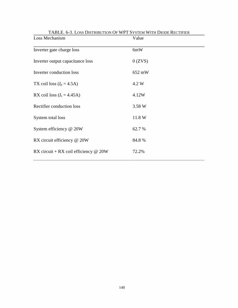
140
TABLE. 6-3. LOSS DISTRIBUTION OF WPT SYSTEM WITH DIODE RECTIFIER
Loss Mechanism Value
Inverter gate charge loss 6mW
Inverter output capacitance loss 0 (ZVS)
Inverter conduction loss 652 mW
TX coil loss (Ip = 4.5A) 4.2 W
RX coil loss (Is = 4.45A) 4.12W
Rectifier conduction loss 3.58 W
System total loss 11.8 W
System efficiency @ 20W 62.7 %
RX circuit efficiency @ 20W 84.8 %
RX circuit + RX coil efficiency @ 20W 72.2%

141
6.2.2 Diode Rectifier plus 3:1 step-down Buck Converter
The simulation results using a diode bridge rectifier plus a 3:1 Buck converter are shown in
Fig. 6-19. The schematic circuit is given in Fig. 6-19 (a) and the inverter voltage and current,
receiver voltage and current are shown as Vsource and Isource, Vrec and Irec, respectively in Fig. 6-
19(b). The key waveforms of the 3:1 Buck converter is given in Fig. 6-20. The switching node
voltage Vsw, the inductor current IL, the output voltage of the diode rectifier Vbus and the load
voltage Vload are shown.
Since the Buck converter steps down the rectifier output voltage from 15 V to 5 V, resulting
in an increased rectifier impedance, the currents in the primary side and the secondary side are
largely reduced compared to those using a simple diode rectifier. The loss mechanism of a WPT
system using the diode rectifier plus Buck converter is as follows. The calculation of the currents
and voltages are similar to the procedure in the previous section. Note that the Buck converter loss
is not involved in the conduction/switching loss calculation. Instead, the Buck converter loss is
treated separately, using a commercial reference implementation.
1) Conduction loss
The conduction loss consists of the loss from the inverter, the resonant tank, and the rectifier.
The conduction loss calculation is the same in (6-16) – (6-18), and Ip = 2.6A is the primary current
rms value and Is = 1.5A is the secondary current rms value in this case.
2) Switching loss
The switching loss consists of the loss from the inverter switching devices and the diodes on
the receiver side.
Again, the loss mechanism is the same in (6-19) – (6-20).
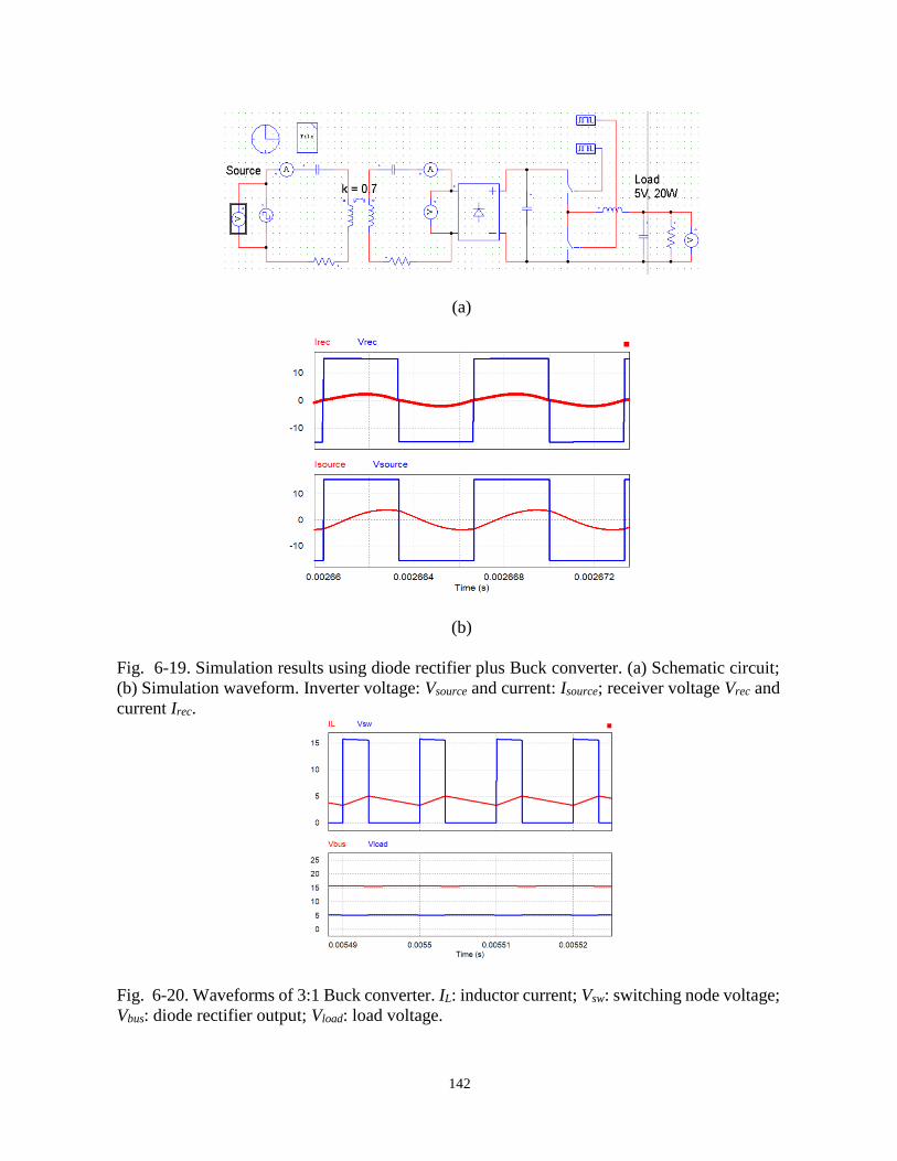
142
(a)
(b)
Fig. 6-19. Simulation results using diode rectifier plus Buck converter. (a) Schematic circuit;
(b) Simulation waveform. Inverter voltage: Vsource and current: Isource; receiver voltage Vrec and
current Irec.
Fig. 6-20. Waveforms of 3:1 Buck converter. IL: inductor current; Vsw: switching node voltage;
Vbus: diode rectifier output; Vload: load voltage.
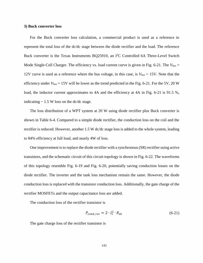
143
3) Buck converter loss
For the Buck converter loss calculation, a commercial product is used as a reference to
represent the total loss of the dc/dc stage between the diode rectifier and the load. The reference
Buck converter is the Texas Instruments BQ25910, an I2C Controlled 6A Three-Level Switch
Mode Single-Cell Charger. The efficiency vs. load current curve is given in Fig. 6-21. The Vbus =
12V curve is used as a reference where the bus voltage, in this case, is Vbus = 15V. Note that the
efficiency under Vbus = 15V will be lower as the trend predicted in the Fig. 6-21. For the 5V, 20 W
load, the inductor current approximates to 4A and the efficiency at 4A in Fig. 6-21 is 91.5 %,
indicating ~ 1.5 W loss on the dc/dc stage.
The loss distribution of a WPT system at 20 W using diode rectifier plus Buck converter is
shown in Table 6-4. Compared to a simple diode rectifier, the conduction loss on the coil and the
rectifier is reduced. However, another 1.5 W dc/dc stage loss is added to the whole system, leading
to 84% efficiency at full load, and nearly 4W of loss.
One improvement is to replace the diode rectifier with a synchronous (SR) rectifier using active
transistors, and the schematic circuit of this circuit topology is shown in Fig. 6-22. The waveforms
of this topology resemble Fig. 6-19 and Fig. 6-20, potentially saving conduction losses on the
diode rectifier. The inverter and the tank loss mechanism remain the same. However, the diode
conduction loss is replaced with the transistor conduction loss. Additionally, the gate charge of the
rectifier MOSFETs and the output capacitance loss are added.
The conduction loss of the rectifier transistor is
𝑃𝑐𝑜𝑛𝑑_𝑟𝑒𝑐 = 2 ∙ 𝐼𝑠2 ∙ 𝑅𝑑𝑠 (6-21)
The gate charge loss of the rectifier transistor is
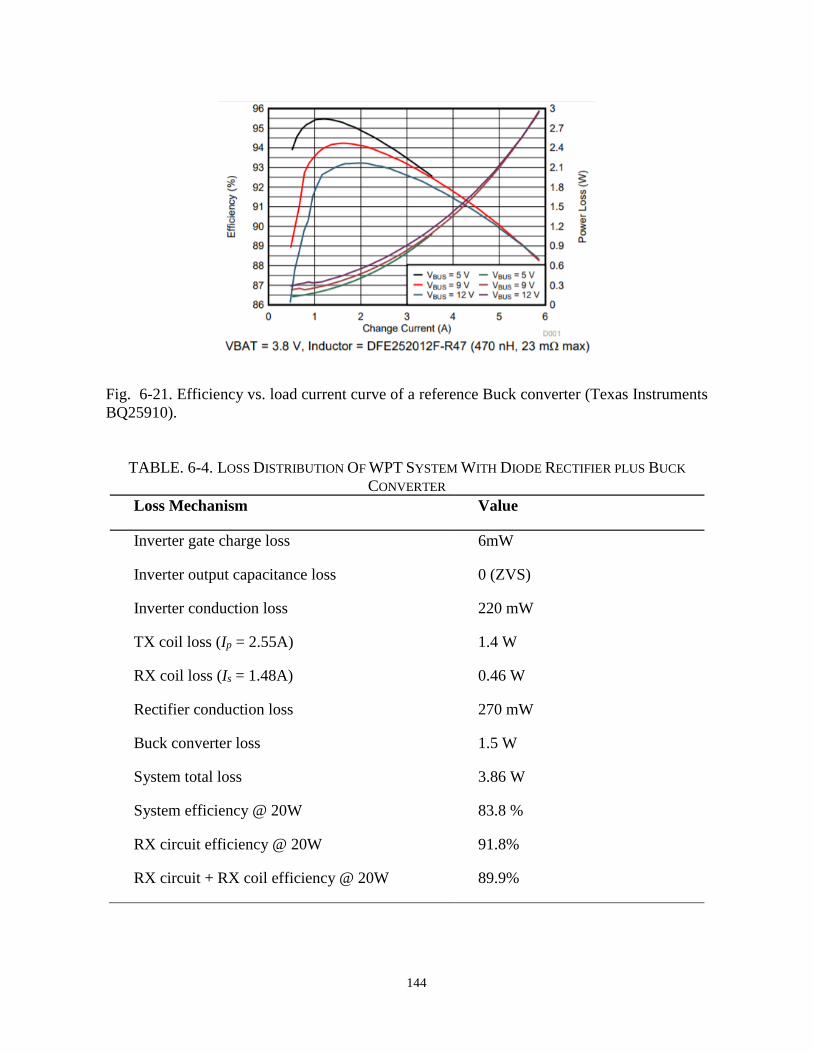
144
Fig. 6-21. Efficiency vs. load current curve of a reference Buck converter (Texas Instruments
BQ25910).
TABLE. 6-4. LOSS DISTRIBUTION OF WPT SYSTEM WITH DIODE RECTIFIER PLUS BUCK
CONVERTER
Loss Mechanism Value
Inverter gate charge loss 6mW
Inverter output capacitance loss 0 (ZVS)
Inverter conduction loss 220 mW
TX coil loss (Ip = 2.55A) 1.4 W
RX coil loss (Is = 1.48A) 0.46 W
Rectifier conduction loss 270 mW
Buck converter loss 1.5 W
System total loss 3.86 W
System efficiency @ 20W 83.8 %
RX circuit efficiency @ 20W 91.8%
RX circuit + RX coil efficiency @ 20W 89.9%

145
𝑃𝑔𝑠_𝑟𝑒𝑐 = 4 ∙ 𝑉𝑔𝑠 ∙ 𝑄𝑔𝑠 ∙ 𝑓𝑠 (6-22)
The output capacitance of the transistor in the rectifier may cause switching related loss
𝑃𝑐𝑜𝑠𝑠_𝑟𝑒𝑐 = 4 ∙ 𝑉𝑑𝑠 ∙ 𝑄𝑜𝑠𝑠 ∙ 𝑓𝑠 (6-23)
The loss distribution of this topology is re-calculated in TABLE 6-5. Though the rectifier
conduction loss is reduced from 270 mW to 70 mW, and the system efficiency increases 1%. The
Buck converter loss remains a significant contributor to the total loss, as the loss of the Buck
converter is close to the tank conduction loss.
6.2.3 Synchronous Rectifier Plus Switched-Capacitor DC/DC Converter
The simulation results using a synchronous rectifier plus a 3:1 Ladder switched-capacitor (SC)
converter are shown in Fig. 6-23. The schematic circuit is given in Fig. 6-23 (a) and the inverter
voltage and current, receiver voltage and current are shown as Vsource and Isource, Vrec and Irec,
respectively in Fig. 6-23(b). The key waveforms of the 3:1 SC converter are given in Fig. 6-24.
The voltage VCx of flying capacitors, the output voltage of the synchronous rectifier Vbus, and the
load voltage Vload are shown.
The loss mechanisms of this design are similar to that of the SR rectifier plus Buck converter.
Major loss mechanism of the synchronous rectifier plus 3:1 Ladder SC converter is demonstrated
as follows.
1) Conduction loss
The conduction loss consists of the loss from the inverter, the resonant tank, and the rectifier.
The conduction loss calculation is the same as in (6-16) – (6-18) and (6-21) - (6-23), where Ip =
2.6A is the primary current rms value and Is = 1.5A is the secondary current rms value in this case.
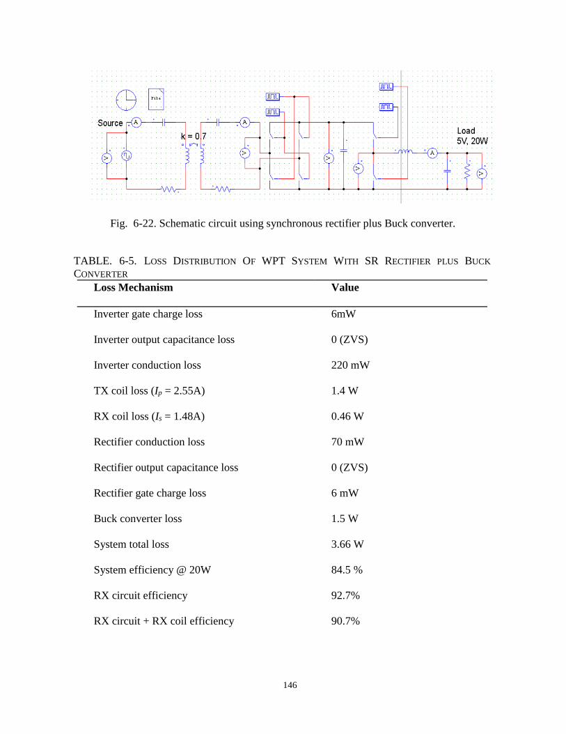
146
Fig. 6-22. Schematic circuit using synchronous rectifier plus Buck converter.
TABLE. 6-5. LOSS DISTRIBUTION OF WPT SYSTEM WITH SR RECTIFIER PLUS BUCK
CONVERTER
Loss Mechanism Value
Inverter gate charge loss 6mW
Inverter output capacitance loss 0 (ZVS)
Inverter conduction loss 220 mW
TX coil loss (Ip = 2.55A) 1.4 W
RX coil loss (Is = 1.48A) 0.46 W
Rectifier conduction loss 70 mW
Rectifier output capacitance loss 0 (ZVS)
Rectifier gate charge loss 6 mW
Buck converter loss 1.5 W
System total loss 3.66 W
System efficiency @ 20W 84.5 %
RX circuit efficiency 92.7%
RX circuit + RX coil efficiency 90.7%
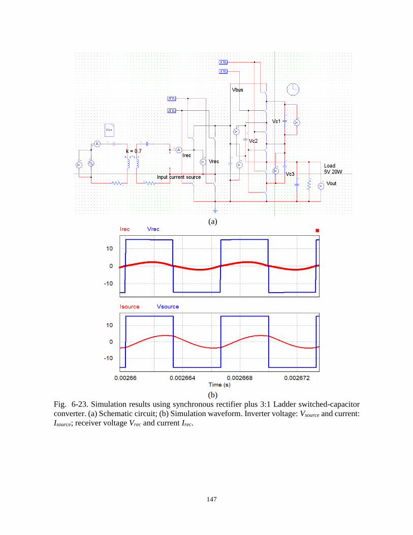
147
(a)
(b)
Fig. 6-23. Simulation results using synchronous rectifier plus 3:1 Ladder switched-capacitor
converter. (a) Schematic circuit; (b) Simulation waveform. Inverter voltage: Vsource and current:
Isource; receiver voltage Vrec and current Irec.
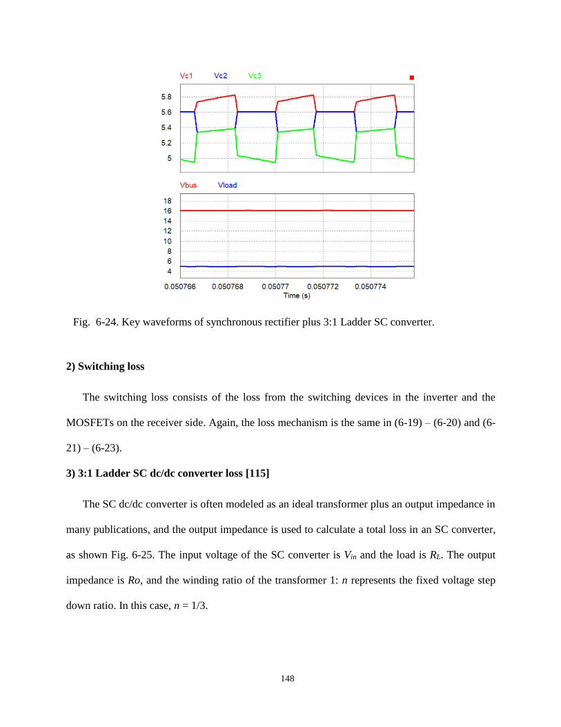
148
2) Switching loss
The switching loss consists of the loss from the switching devices in the inverter and the
MOSFETs on the receiver side. Again, the loss mechanism is the same in (6-19) – (6-20) and (6-
21) – (6-23).
3) 3:1 Ladder SC dc/dc converter loss [115]
The SC dc/dc converter is often modeled as an ideal transformer plus an output impedance in
many publications, and the output impedance is used to calculate a total loss in an SC converter,
as shown Fig. 6-25. The input voltage of the SC converter is Vin and the load is RL. The output
impedance is Ro, and the winding ratio of the transformer 1: n represents the fixed voltage step
down ratio. In this case, n = 1/3.
Fig. 6-24. Key waveforms of synchronous rectifier plus 3:1 Ladder SC converter.
149
The operation of the 3:1 Ladder SC converter has two subintervals. In the subinterval 1, the
input voltage is in series with the flying capacitor and the load. In the subinterval 2, the input
voltage is disconnected, and the flying capacitor is clamped to the load, discharging. The schematic
circuits of the two-subinterval operation are given in Fig. 6-26 [115].
The major loss mechanism in the switched-capacitor converter is the charge sharing loss, and
it is proportional to the capacitance and the switching frequency. This loss is frequency dependent,
and two equations are used to approximate the output impedance Ro at different frequencies. When
the switching frequency is far below the RC constant of the circuit, the SC converter is in the slow
switching limit (SSL). When the switching frequency is comparable with the RC constant of the
circuit, the circuit is in the fast switching limit (FSL) [115][120].
In SSL, the output impedance is
𝑅𝑜 = 𝑅𝑆𝑆𝐿 = ∑𝑎𝑐𝑖
𝐶𝑖 ∙ 𝑓𝑠𝑖
(6-24)
In FSL, the output impedance is
𝑅𝑜 = 𝑅𝐹𝑆𝐿 = 2 ∑ 𝑅𝑖(𝑎𝑠𝑖)2
𝑖
(6-25)
In (6-24) and (6-25), aci is the charge multiplier vector at each flying capacitor; asi is the charge
multiplier vector via each switch; Ci is the capacitance at each node; fs is the frequency, and Ri is
the resistance in each switch; the subscript i represents the ith component in this case.
𝑎𝑐𝑖 = [2
3,1
3,1
3] (6-26)
𝑎𝑠𝑖 = [2
3,2
3,1
3,1
3,1
3,1
3] (6-27)
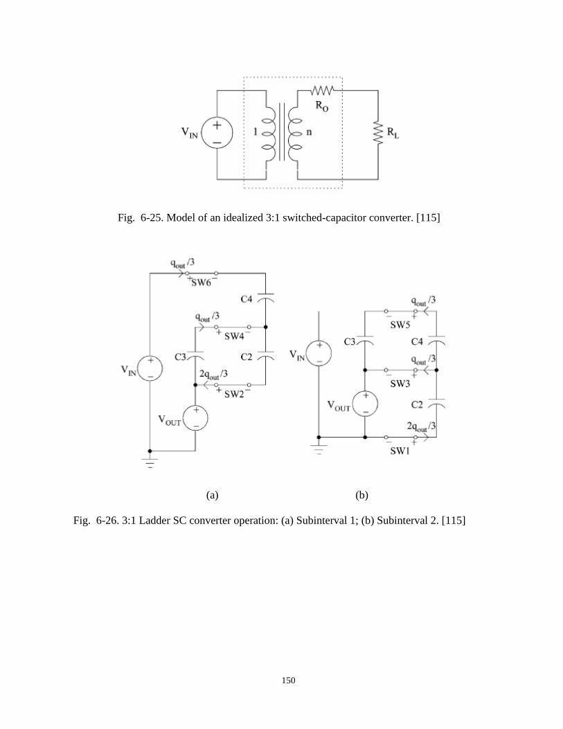
150
Fig. 6-25. Model of an idealized 3:1 switched-capacitor converter. [115]
(a) (b)
Fig. 6-26. 3:1 Ladder SC converter operation: (a) Subinterval 1; (b) Subinterval 2. [115]

151
Assuming the capacitance Cx = 40 µF and Rds(on) = 16 mΩ, two output impedance can be
calculated with (6-26) - (6-27). As a result, RssL = 1/9 Ω and RFSL = 1/25 Ω in this case.
The 1/RC constant of the circuit is 1.67 MHz, and the circuit transits from SSL to FSL around
this frequency. The loss distribution is calculated using two frequencies, fs = 150 kHz and fs = 2
MHz as a comparison between SSL and FSL. The switching loss is calculated using (6-19) and (6-
20), the transistor data are the same, with Qgs = 2nC, Qoss = 4nC, Vgs = 5V and Vds = 5V.
A detailed loss distribution is shown in Table 6-6, and two efficiencies with SSL and FSL are
calculated in this table. Compared with the MSC step-down rectifier, the SR rectifier plus 3:1 SC
converter use less flying capacitors, but the efficiency of the system is ηSSL < ηMSC (m = 2.5) <
ηFSL< ηMSC (m = 3.81). The design can achieve a higher power density, but lack of an output
regulation ability.
6.2.4 Seven-level Switched Capacitor 3:1 step-down AC-DC Rectifier
The simulation results using a 7-level Switched Capacitor 3:1 step-down ac-dc rectifier are
shown in Fig. 6-27. The schematic circuit is given in Fig. 6-23 (a) and the inverter voltage and
current, receiver voltage and current are shown as Vsource and Isource, Vrec and Irec, respectively in
Fig. 6-27(b).
In order to simplify analysis, two assumptions are made about the converter design: 1) All
flying capacitors are large enough to ensure small voltage ripple, and the output capacitance Cout
is sufficient to ensure a constant Vload; 2) All subinterval durations are much longer than the
switched capacitor circuit internal RC dynamics, so that the slow switching limit (SSL) applies at
given switching frequency (150 kHz). Under these assumptions, the flying capacitor voltages are
approximately dc, with magnitude equal to the load voltage Vload.
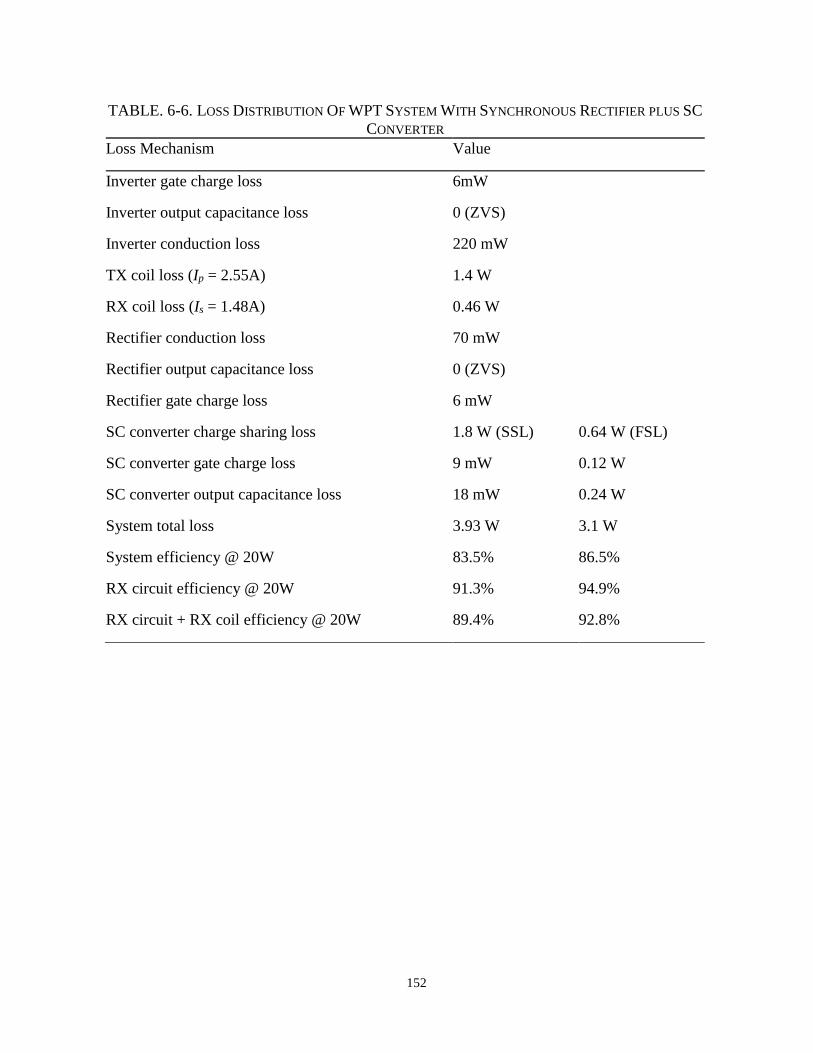
152
TABLE. 6-6. LOSS DISTRIBUTION OF WPT SYSTEM WITH SYNCHRONOUS RECTIFIER PLUS SC
CONVERTER
Loss Mechanism Value
Inverter gate charge loss 6mW
Inverter output capacitance loss 0 (ZVS)
Inverter conduction loss 220 mW
TX coil loss (Ip = 2.55A) 1.4 W
RX coil loss (Is = 1.48A) 0.46 W
Rectifier conduction loss 70 mW
Rectifier output capacitance loss 0 (ZVS)
Rectifier gate charge loss 6 mW
SC converter charge sharing loss 1.8 W (SSL) 0.64 W (FSL)
SC converter gate charge loss 9 mW 0.12 W
SC converter output capacitance loss 18 mW 0.24 W
System total loss 3.93 W 3.1 W
System efficiency @ 20W 83.5% 86.5%
RX circuit efficiency @ 20W 91.3% 94.9%
RX circuit + RX coil efficiency @ 20W 89.4% 92.8%
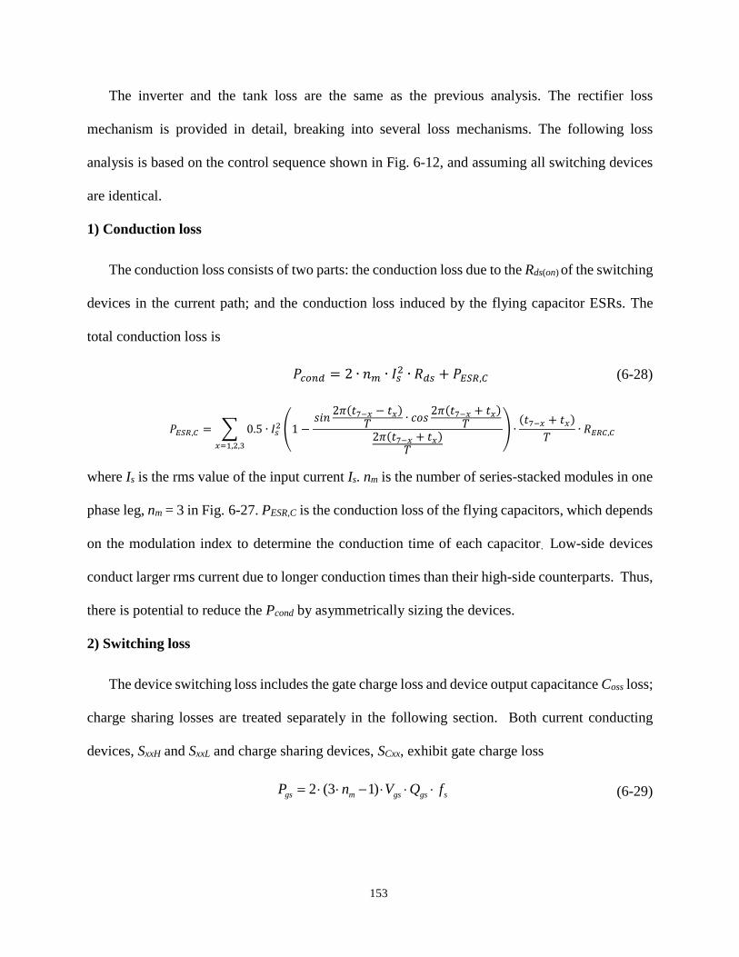
153
The inverter and the tank loss are the same as the previous analysis. The rectifier loss
mechanism is provided in detail, breaking into several loss mechanisms. The following loss
analysis is based on the control sequence shown in Fig. 6-12, and assuming all switching devices
are identical.
1) Conduction loss
The conduction loss consists of two parts: the conduction loss due to the Rds(on) of the switching
devices in the current path; and the conduction loss induced by the flying capacitor ESRs. The
total conduction loss is
𝑃𝑐𝑜𝑛𝑑 = 2 ∙ 𝑛𝑚 ∙ 𝐼𝑠2 ∙ 𝑅𝑑𝑠 + 𝑃𝐸𝑆𝑅,𝐶 (6-28)
𝑃𝐸𝑆𝑅,𝐶 = ∑ 0.5 ∙ 𝐼𝑠 2 (1 −
𝑠𝑖𝑛2𝜋(𝑡7−𝑥 − 𝑡𝑥)
𝑇∙ 𝑐𝑜𝑠
2𝜋(𝑡7−𝑥 + 𝑡𝑥)𝑇
2𝜋(𝑡7−𝑥 + 𝑡𝑥)𝑇
) ∙(𝑡7−𝑥 + 𝑡𝑥)
𝑇∙ 𝑅𝐸𝑅𝐶,𝐶
𝑥=1,2,3
where Is is the rms value of the input current Is. nm is the number of series-stacked modules in one
phase leg, nm = 3 in Fig. 6-27. PESR,C is the conduction loss of the flying capacitors, which depends
on the modulation index to determine the conduction time of each capacitor. Low-side devices
conduct larger rms current due to longer conduction times than their high-side counterparts. Thus,
there is potential to reduce the Pcond by asymmetrically sizing the devices.
2) Switching loss
The device switching loss includes the gate charge loss and device output capacitance Coss loss;
charge sharing losses are treated separately in the following section. Both current conducting
devices, SxxH and SxxL and charge sharing devices, SCxx, exhibit gate charge loss
2 (3 1)gs m gs gs sP n V Q f (6-29)
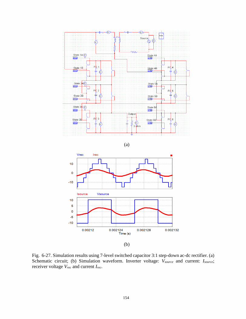
154
(a)
(b)
Fig. 6-27. Simulation results using 7-level switched capacitor 3:1 step-down ac-dc rectifier. (a)
Schematic circuit; (b) Simulation waveform. Inverter voltage: Vsource and current: Isource;
receiver voltage Vrec and current Irec.
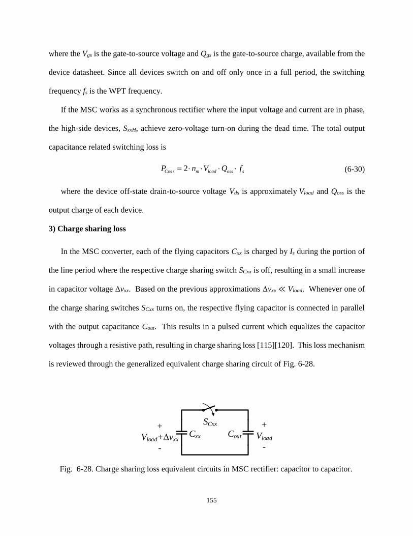
155
where the Vgs is the gate-to-source voltage and Qgs is the gate-to-source charge, available from the
device datasheet. Since all devices switch on and off only once in a full period, the switching
frequency fs is the WPT frequency.
If the MSC works as a synchronous rectifier where the input voltage and current are in phase,
the high-side devices, SxxH, achieve zero-voltage turn-on during the dead time. The total output
capacitance related switching loss is
Cos 2s m load oss sP n V Q f (6-30)
where the device off-state drain-to-source voltage Vds is approximately Vload and Qoss is the
output charge of each device.
3) Charge sharing loss
In the MSC converter, each of the flying capacitors Cxx is charged by Is during the portion of
the line period where the respective charge sharing switch SCxx is off, resulting in a small increase
in capacitor voltage Δvxx. Based on the previous approximations Δvxx ≪ Vload. Whenever one of
the charge sharing switches SCxx turns on, the respective flying capacitor is connected in parallel
with the output capacitance Cout. This results in a pulsed current which equalizes the capacitor
voltages through a resistive path, resulting in charge sharing loss [115][120]. This loss mechanism
is reviewed through the generalized equivalent charge sharing circuit of Fig. 6-28.
Cxx Cout
+
Vload+Δvxx
-
+
Vload
-
SCxx
Fig. 6-28. Charge sharing loss equivalent circuits in MSC rectifier: capacitor to capacitor.

156
In Fig. 6-28, if Δvxx = 0, no loss occurs when the switch closes. However, if a small voltage
difference Δvxx is present, then the total charge among two capacitors will re-distribute as the two
capacitor voltages equalize after turning the switch ON. Assuming an incremental voltage Δvxx of
the flying capacitor Cxx, and the output capacitance Cout is large enough for a constant Vload,
Cout ≫ Cxx, then the charge sharing loss is
𝑃𝑐𝑠 = 0.5 ∙ 𝐶𝑥𝑥 ∙ ∆𝑉𝑥𝑥2 ∙ 𝑓𝑠 (6-31)
6.2.5 Charge Control for MSC Rectifier
From (6-31), the charge sharing loss, which can be significant in hard-charging SC converters,
is proportional to the switching frequency, capacitance and the segment of the voltage ripple on
flying capacitors, the latter of which depends on the control strategy of the MSC rectifier. Two
representative charge control schemes are studied to minimize the charge sharing loss under
different operating points in the following section.
1) Stack charge control
The stack charge control means that flying capacitors are charged in a stacked flow, being last-
in, first-out (LIFO) sequence, as demonstrated in Fig. 6-12. The top flying capacitor charges first
and switches out last, while the bottom one charges last, but pops out first. Since the voltage ripple
on each flying capacitor is proportional to the charge sharing loss, the voltage ripples are calculated
as follows.
Using the proposed 7-level MSC as an example, C1A has total input charge q1 in the positive-
current half-period
𝑞1 = ∫ 𝐼𝑖𝑛sin(𝜔𝑠𝑡)𝑑𝑡𝑡6
𝑡1
(6-32)
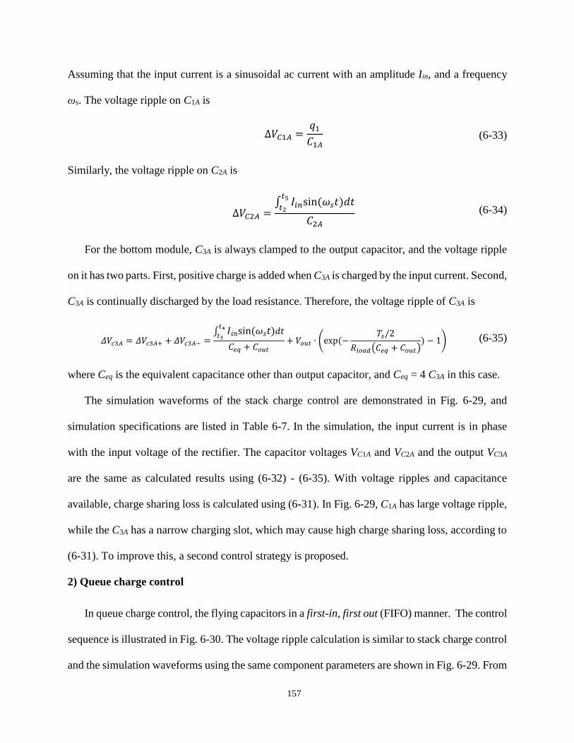
157
Assuming that the input current is a sinusoidal ac current with an amplitude Iin, and a frequency
ωs. The voltage ripple on C1A is
∆𝑉𝐶1𝐴 =𝑞1
𝐶1𝐴 (6-33)
Similarly, the voltage ripple on C2A is
∆𝑉𝐶2𝐴 =∫ 𝐼𝑖𝑛sin(𝜔𝑠𝑡)𝑑𝑡
𝑡5
𝑡2
𝐶2𝐴 (6-34)
For the bottom module, C3A is always clamped to the output capacitor, and the voltage ripple
on it has two parts. First, positive charge is added when C3A is charged by the input current. Second,
C3A is continually discharged by the load resistance. Therefore, the voltage ripple of C3A is
𝛥𝑉𝑐3𝐴 = 𝛥𝑉𝑐3𝐴+ + 𝛥𝑉𝑐3𝐴− =∫ 𝐼𝑖𝑛sin(𝜔𝑠𝑡)𝑑𝑡
𝑡4
𝑡3
𝐶𝑒𝑞 + 𝐶𝑜𝑢𝑡
+ 𝑉𝑜𝑢𝑡 ∙ (exp (−𝑇𝑠/2
𝑅𝑙𝑜𝑎𝑑(𝐶𝑒𝑞 + 𝐶𝑜𝑢𝑡)) − 1) (6-35)
where Ceq is the equivalent capacitance other than output capacitor, and Ceq = 4 C3A in this case.
The simulation waveforms of the stack charge control are demonstrated in Fig. 6-29, and
simulation specifications are listed in Table 6-7. In the simulation, the input current is in phase
with the input voltage of the rectifier. The capacitor voltages VC1A and VC2A and the output VC3A
are the same as calculated results using (6-32) - (6-35). With voltage ripples and capacitance
available, charge sharing loss is calculated using (6-31). In Fig. 6-29, C1A has large voltage ripple,
while the C3A has a narrow charging slot, which may cause high charge sharing loss, according to
(6-31). To improve this, a second control strategy is proposed.
2) Queue charge control
In queue charge control, the flying capacitors in a first-in, first out (FIFO) manner. The control
sequence is illustrated in Fig. 6-30. The voltage ripple calculation is similar to stack charge control
and the simulation waveforms using the same component parameters are shown in Fig. 6-29. From
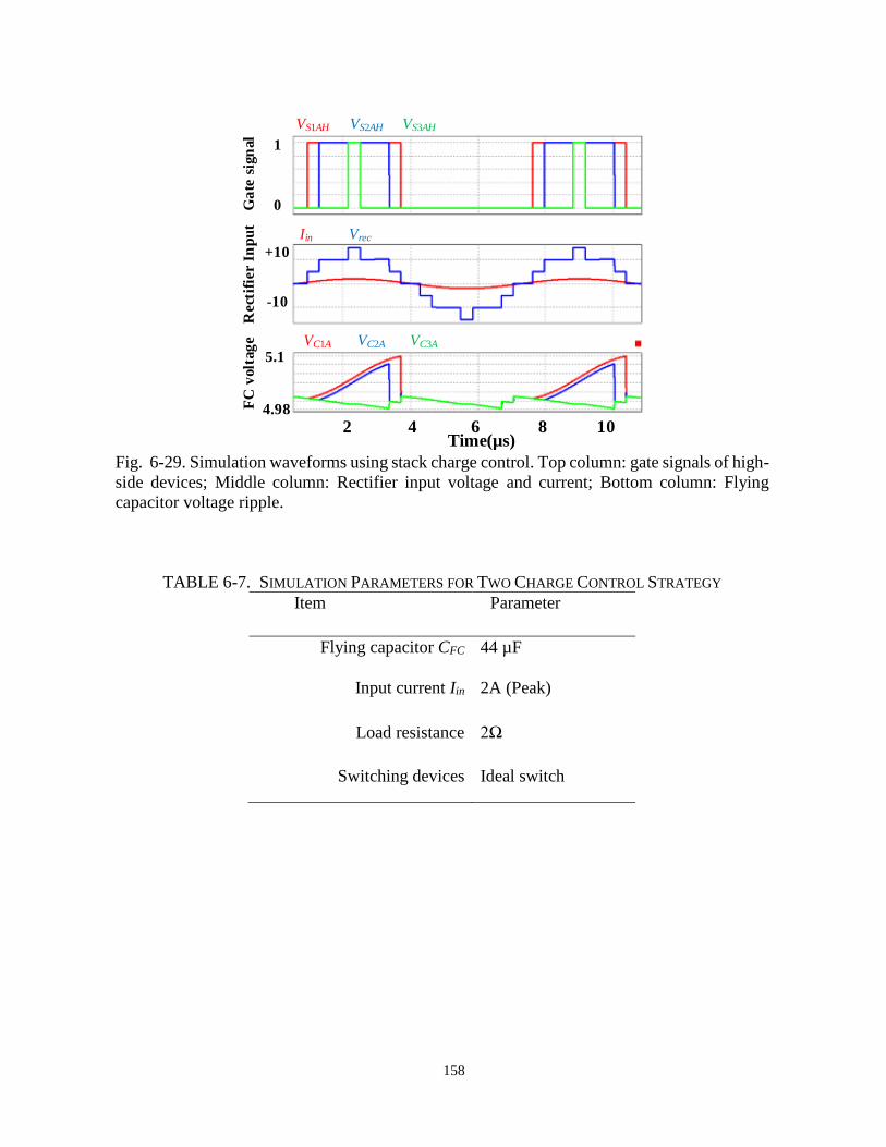
158
2 4 6 8 10Time(µs)
0
1
-10
+10
4.98
5.1
Ga
te s
ign
al
Rect
ifie
r I
np
ut
FC
volt
ag
e
VS1AH VS2AH VS3AH
Iin Vrec
VC1A VC2A VC3A
Fig. 6-29. Simulation waveforms using stack charge control. Top column: gate signals of high-
side devices; Middle column: Rectifier input voltage and current; Bottom column: Flying
capacitor voltage ripple.
TABLE 6-7. SIMULATION PARAMETERS FOR TWO CHARGE CONTROL STRATEGY
Item Parameter
Flying capacitor CFC 44 µF
Input current Iin 2A (Peak)
Load resistance 2Ω
Switching devices Ideal switch

159
the simulation results, it is observed that ΔVC1A is reduced. This difference, in the simulated
operating point, reduces the hard-charging loss by about 50% compared to the stack charge control
case.
Both the stack charge control example in Fig. 6-29 and the queue charge control example in
Fig. 6-31 assume the rectifier is controlled so that the fundamental components of Vrec and Iin are
in phase. However, in some applications, the rectifier may adjust phase-shift between the input
voltage and current to maximize extractable power. As the input current phase changes, the relative
merits of each control scheme will vary. Fig. 6-28 repeats the simulation for both methods, using
the same parameters in Table 6-1, but with the input current leading the voltage by a varied phase
angle. Both charge sharing losses are normalized using a loss base of the queue charge control
with 0VI . In this case, the voltage ripple of each capacitor, and consequently the charge sharing
losses, are smaller if using stack charge control, rather than queue charge control in the region of
(40 ,90 )VI .
In this tightly coupled WPT system (k = 0.7), the MSC rectifier works as a SR rectifier to
minimize both the primary and secondary current amplitudes and therefore conduction loss. As a
result, the phase angle φvi between the rectifier voltage and current is nearly zero. Based on the
analysis in Fig. 6-32, the queue charge control is beneficial in this case to reduce the charge sharing
loss.
160
MSC
Input Iin
VREC
T/2t1 t2 t3 t4 t5 t6
SC1A
SC2A
S1AH(S1AL)
S2AH(S2AL)
S3AH(S3AL)
Fig. 6-30. Queue charge control sequence for 7-level MSC rectifier in half line cycle. Solid
line: high side switch and charge sharing switch (S1AH, S2AH, S3AH, SC1A, SC2A); dash line: low
side switch (S1AL, S2AL, S3AL).
0
1
-10
+10
4.98
5.08
0 2 4 6 8 10Time(µs)
Ga
te s
ign
al
Rect
ifie
r I
np
ut
FC
volt
ag
e
VS1AH VS2AH VS3AH
Iin Vrec
VC1A VC2A VC3A
Fig. 6-31. Simulation waveforms using queue charge control. Top column: gate signals of
high-side devices; Middle column: Rectifier input voltage and current; Bottom column: Flying
capacitor voltage ripple.
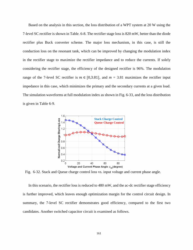
161
Based on the analysis in this section, the loss distribution of a WPT system at 20 W using the
7-level SC rectifier is shown in Table. 6-8. The rectifier stage loss is 820 mW, better than the diode
rectifier plus Buck converter scheme. The major loss mechanism, in this case, is still the
conduction loss on the resonant tank, which can be improved by changing the modulation index
in the rectifier stage to maximize the rectifier impedance and to reduce the currents. If solely
considering the rectifier stage, the efficiency of the designed rectifier is 96%. The modulation
range of the 7-level SC rectifier is 𝑚 ∈ [0,3.81], and m = 3.81 maximizes the rectifier input
impedance in this case, which minimizes the primary and the secondary currents at a given load.
The simulation waveforms at full modulation index as shown in Fig. 6-33, and the loss distribution
is given in Table 6-9.
In this scenario, the rectifier loss is reduced to 480 mW, and the ac-dc rectifier stage efficiency
is further improved, which leaves enough optimization margin for the control circuit design. In
summary, the 7-level SC rectifier demonstrates good efficiency, compared to the first two
candidates. Another switched capacitor circuit is examined as follows.
Stack Charge Control
Queue Charge Control
Fig. 6-32. Stack and Queue charge control loss vs. input voltage and current phase angle.
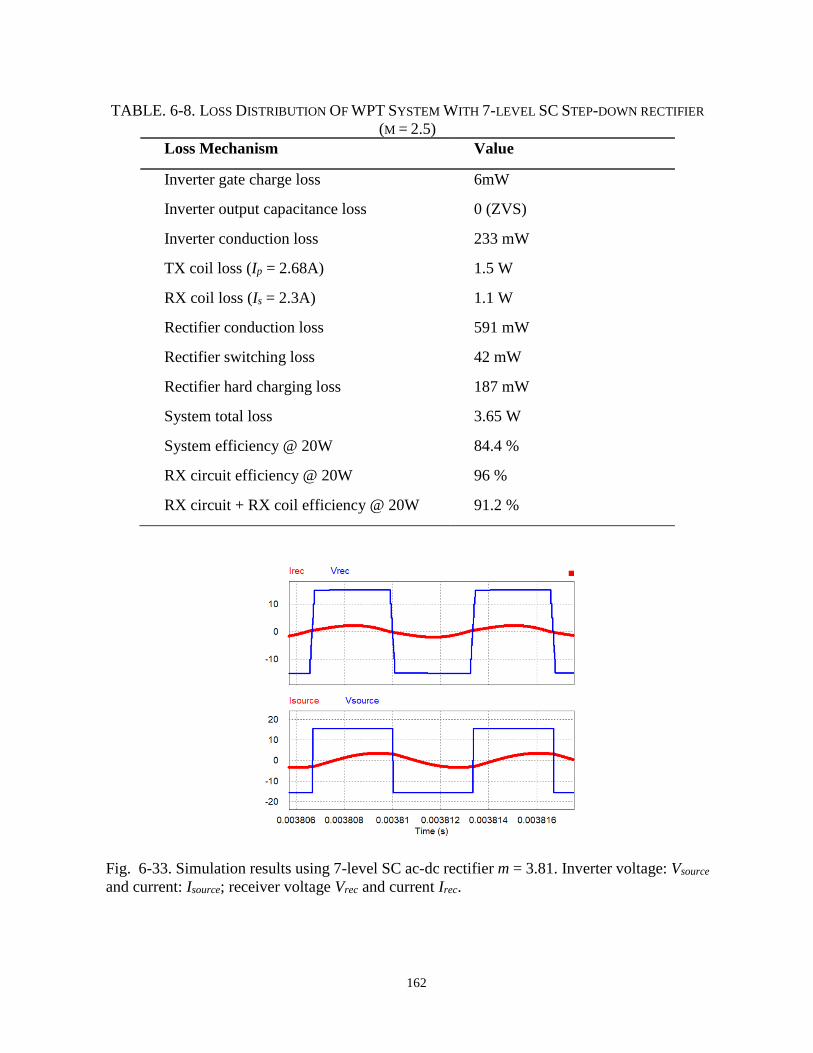
162
TABLE. 6-8. LOSS DISTRIBUTION OF WPT SYSTEM WITH 7-LEVEL SC STEP-DOWN RECTIFIER
(M = 2.5)
Loss Mechanism Value
Inverter gate charge loss 6mW
Inverter output capacitance loss 0 (ZVS)
Inverter conduction loss 233 mW
TX coil loss (Ip = 2.68A) 1.5 W
RX coil loss (Is = 2.3A) 1.1 W
Rectifier conduction loss 591 mW
Rectifier switching loss 42 mW
Rectifier hard charging loss 187 mW
System total loss 3.65 W
System efficiency @ 20W 84.4 %
RX circuit efficiency @ 20W 96 %
RX circuit + RX coil efficiency @ 20W 91.2 %
Fig. 6-33. Simulation results using 7-level SC ac-dc rectifier m = 3.81. Inverter voltage: Vsource
and current: Isource; receiver voltage Vrec and current Irec.
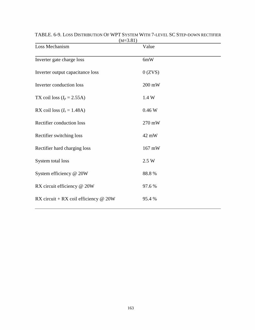
163
TABLE. 6-9. LOSS DISTRIBUTION OF WPT SYSTEM WITH 7-LEVEL SC STEP-DOWN RECTIFIER
(M=3.81)
Loss Mechanism Value
Inverter gate charge loss 6mW
Inverter output capacitance loss 0 (ZVS)
Inverter conduction loss 200 mW
TX coil loss (Ip = 2.55A) 1.4 W
RX coil loss (Is = 1.48A) 0.46 W
Rectifier conduction loss 270 mW
Rectifier switching loss 42 mW
Rectifier hard charging loss 167 mW
System total loss 2.5 W
System efficiency @ 20W 88.8 %
RX circuit efficiency @ 20W 97.6 %
RX circuit + RX coil efficiency @ 20W 95.4 %

164
6.2.6 Summary
Four candidates, 1) diode rectifier; 2) diode rectifier plus 3:1 Buck converter; 3) 7-level
switched-capacitor step-down rectifier and 4) synchronous rectifier plus 3:1 Ladder SC converter,
are compared regarding efficiency in this section. The detailed derivations of loss equations are
provided, and the distributed loss, total loss, and efficiency summary are given in tables.
A summary is demonstrated in Table 6-10, where the total loss of the WPT system employing
different rectifiers is shown. The improved loss is given for each candidate, such as using a
synchronous rectifier, changing the modulation index or change the operation frequency. The
system efficiency is provided in the table. From Table 6-10, the MSC rectifier reaches the highest
efficiency, and possesses regulation ability.
TABLE. 6-10. LOSS AND EFFICIENCY COMPARISON OF FOUR CANDIDATES
Candidate 1 Candidate 2 Candidate 3 Candidate 4
m=2.5 m=3.81
Total loss 11.8 W 3.86 W 3.68 W 2.5 W 3.93 W
System efficiency 62.7 % 84.5 % 84.4 % 88.8 % 86.5%
RX circuit efficiency 84.8 % 91.8% 96 % 97.6 % 94.9%
RX circuit+coil efficiency 72.2% 89.9% 91.2 % 95.4 % 92.8%
Regulation freedom N/A duty cycle modulation index N/A
*Candidate 1: Diode rectifier
*Candidate 2: diode rectifier plus 3:1 Buck converter
*Candidate 3: 7-level switched-capacitor step-down rectifier
*Candidate 4: synchronous rectifier plus 3:1 Ladder SC converter
165
6.3 THD Analysis
In a WPT system, the transmitter and the receiver are power electronics converters that
generate harmonic content, as shown in Fig. 6-34. In this narrowband system that limits its
operation frequency, the harmonic content that falls out of the allowable band needs to be
attenuated below certain standards. Additional passive filters are employed on the receiver to
achieve this attenuation. Those passive filters, however, take space on the space-constrained
mobile devices, which adds difficulties for a compact design. The current THD is a factor
determining the additional filter design and EMI design of wireless charging systems. With
different rectifiers, the performance of current THD varies.
In this section, the current THD is analyzed using the circuit model of WPT system, and three
factors that determine the current THD are identified. The current THD of the four candidates are
given, and an approach that can minimize the harmonic content is investigated.
6.3.1 Current THD modeling
The schematic circuit that models the current THD is shown in Fig. 6-34. In Fig. 6-34(a), the
output voltage of the inverter is assumed a square wave and a controllable voltage is shown as the
rectifier. In the spectra of both the transmitter and the rectifier, not only the fundamental frequency
but also its harmonics exist, as shown in Fig. 6-35. The fundamental, the 3rd and the 5th, are selected
in the simplified circuit model, shown in Fig. 6-34(b) to model the current THD.
For a square wave inverter output, the amplitudes of each frequency are
𝑉𝑖𝑛𝑣 ≈4
𝜋𝑉𝑑𝑐 sin(𝜔𝑡) +
4
3𝜋𝑉𝑑𝑐 sin(3𝜔𝑡) +
4
5𝜋𝑉𝑑𝑐 sin(5𝜔𝑡) (6-36)
For a controllable rectifier input, the amplitudes of each frequency are
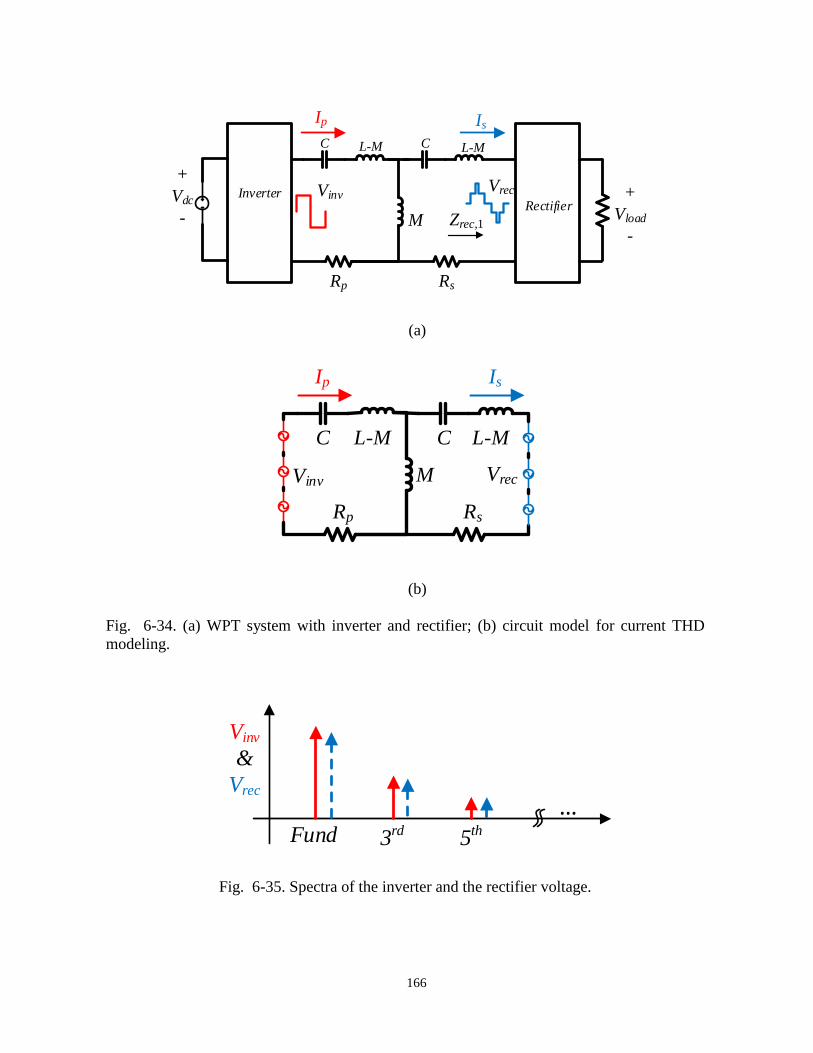
166
C L-M L-MC
M
VrecVinv +
Vload
-
Ip Is
Zrec,1
Rp Rs
Rectifier
+
Vdc
-
Inverter
(a)
Vinv
C L-M L-MC
M Vrec
Ip Is
Rp Rs
(b)
Fig. 6-34. (a) WPT system with inverter and rectifier; (b) circuit model for current THD
modeling.
Fund 3rd 5th
Vinv
&
Vrec
Fig. 6-35. Spectra of the inverter and the rectifier voltage.
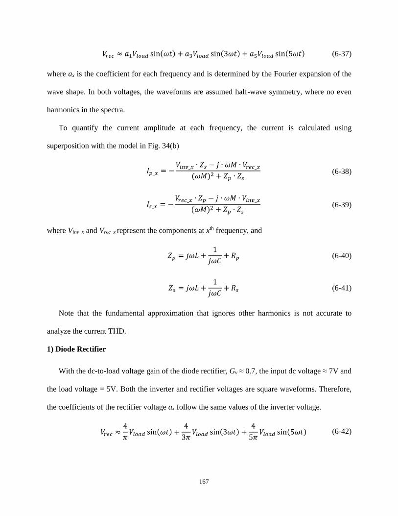
167
𝑉𝑟𝑒𝑐 ≈ 𝑎1𝑉𝑙𝑜𝑎𝑑 sin(𝜔𝑡) + 𝑎3𝑉𝑙𝑜𝑎𝑑 sin(3𝜔𝑡) + 𝑎5𝑉𝑙𝑜𝑎𝑑 sin(5𝜔𝑡) (6-37)
where ax is the coefficient for each frequency and is determined by the Fourier expansion of the
wave shape. In both voltages, the waveforms are assumed half-wave symmetry, where no even
harmonics in the spectra.
To quantify the current amplitude at each frequency, the current is calculated using
superposition with the model in Fig. 34(b)
𝐼𝑝_𝑥 = −𝑉𝑖𝑛𝑣_𝑥 ∙ 𝑍𝑠 − 𝑗 ∙ 𝜔𝑀 ∙ 𝑉𝑟𝑒𝑐_𝑥
(𝜔𝑀)2 + 𝑍𝑝 ∙ 𝑍𝑠 (6-38)
𝐼𝑠_𝑥 = −𝑉𝑟𝑒𝑐_𝑥 ∙ 𝑍𝑝 − 𝑗 ∙ 𝜔𝑀 ∙ 𝑉𝑖𝑛𝑣_𝑥
(𝜔𝑀)2 + 𝑍𝑝 ∙ 𝑍𝑠 (6-39)
where Vinv_x and Vrec_x represent the components at xth frequency, and
𝑍𝑝 = 𝑗𝜔𝐿 +1
𝑗𝜔𝐶+ 𝑅𝑝 (6-40)
𝑍𝑠 = 𝑗𝜔𝐿 +1
𝑗𝜔𝐶+ 𝑅𝑠 (6-41)
Note that the fundamental approximation that ignores other harmonics is not accurate to
analyze the current THD.
1) Diode Rectifier
With the dc-to-load voltage gain of the diode rectifier, Gv ≈ 0.7, the input dc voltage ≈ 7V and
the load voltage = 5V. Both the inverter and rectifier voltages are square waveforms. Therefore,
the coefficients of the rectifier voltage ax follow the same values of the inverter voltage.
𝑉𝑟𝑒𝑐 ≈4
𝜋𝑉𝑙𝑜𝑎𝑑 sin(𝜔𝑡) +
4
3𝜋𝑉𝑙𝑜𝑎𝑑 sin(3𝜔𝑡) +
4
5𝜋𝑉𝑙𝑜𝑎𝑑 sin(5𝜔𝑡) (6-42)
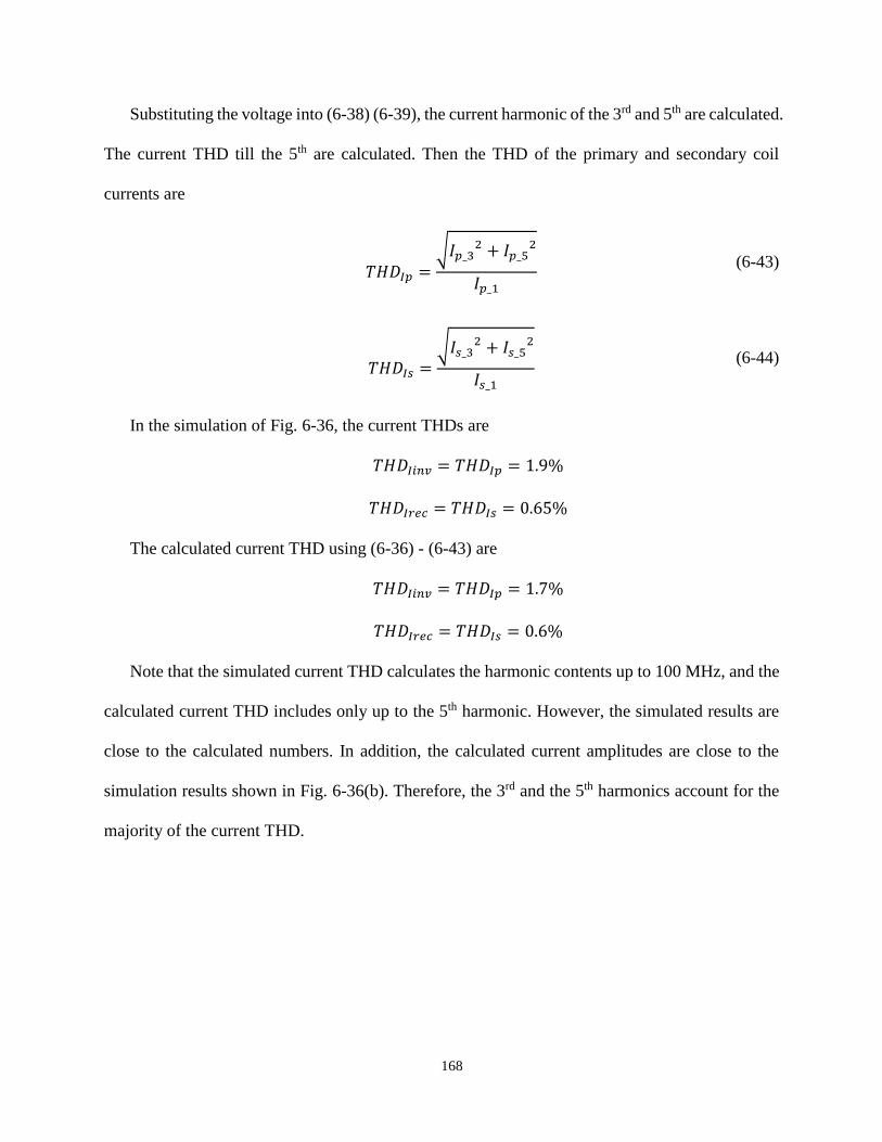
168
Substituting the voltage into (6-38) (6-39), the current harmonic of the 3rd and 5th are calculated.
The current THD till the 5th are calculated. Then the THD of the primary and secondary coil
currents are
𝑇𝐻𝐷𝐼𝑝 =
√𝐼𝑝_32 + 𝐼𝑝_5
2
𝐼𝑝_1
(6-43)
𝑇𝐻𝐷𝐼𝑠 =
√𝐼𝑠_32 + 𝐼𝑠_5
2
𝐼𝑠_1
(6-44)
In the simulation of Fig. 6-36, the current THDs are
𝑇𝐻𝐷𝐼𝑖𝑛𝑣 = 𝑇𝐻𝐷𝐼𝑝 = 1.9%
𝑇𝐻𝐷𝐼𝑟𝑒𝑐 = 𝑇𝐻𝐷𝐼𝑠 = 0.65%
The calculated current THD using (6-36) - (6-43) are
𝑇𝐻𝐷𝐼𝑖𝑛𝑣 = 𝑇𝐻𝐷𝐼𝑝 = 1.7%
𝑇𝐻𝐷𝐼𝑟𝑒𝑐 = 𝑇𝐻𝐷𝐼𝑠 = 0.6%
Note that the simulated current THD calculates the harmonic contents up to 100 MHz, and the
calculated current THD includes only up to the 5th harmonic. However, the simulated results are
close to the calculated numbers. In addition, the calculated current amplitudes are close to the
simulation results shown in Fig. 6-36(b). Therefore, the 3rd and the 5th harmonics account for the
majority of the current THD.
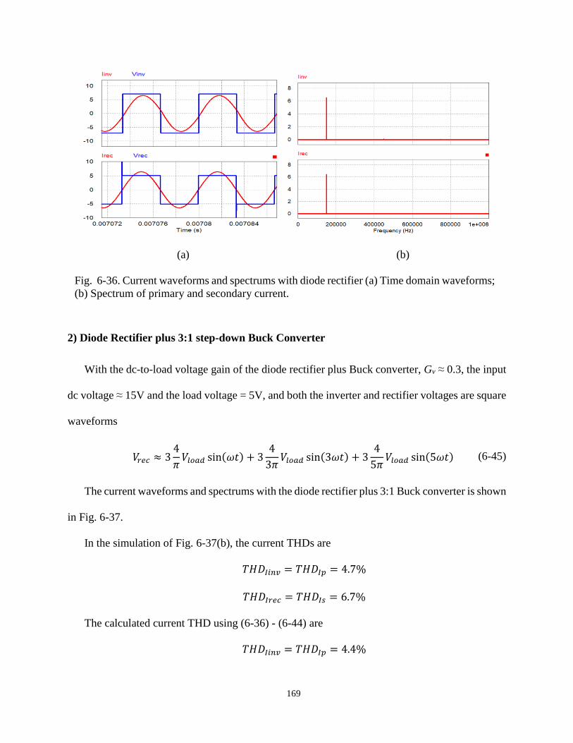
169
2) Diode Rectifier plus 3:1 step-down Buck Converter
With the dc-to-load voltage gain of the diode rectifier plus Buck converter, Gv ≈ 0.3, the input
dc voltage ≈ 15V and the load voltage = 5V, and both the inverter and rectifier voltages are square
waveforms
𝑉𝑟𝑒𝑐 ≈ 34
𝜋𝑉𝑙𝑜𝑎𝑑 sin(𝜔𝑡) + 3
4
3𝜋𝑉𝑙𝑜𝑎𝑑 sin(3𝜔𝑡) + 3
4
5𝜋𝑉𝑙𝑜𝑎𝑑 sin(5𝜔𝑡) (6-45)
The current waveforms and spectrums with the diode rectifier plus 3:1 Buck converter is shown
in Fig. 6-37.
In the simulation of Fig. 6-37(b), the current THDs are
𝑇𝐻𝐷𝐼𝑖𝑛𝑣 = 𝑇𝐻𝐷𝐼𝑝 = 4.7%
𝑇𝐻𝐷𝐼𝑟𝑒𝑐 = 𝑇𝐻𝐷𝐼𝑠 = 6.7%
The calculated current THD using (6-36) - (6-44) are
𝑇𝐻𝐷𝐼𝑖𝑛𝑣 = 𝑇𝐻𝐷𝐼𝑝 = 4.4%
(a) (b)
Fig. 6-36. Current waveforms and spectrums with diode rectifier (a) Time domain waveforms;
(b) Spectrum of primary and secondary current.
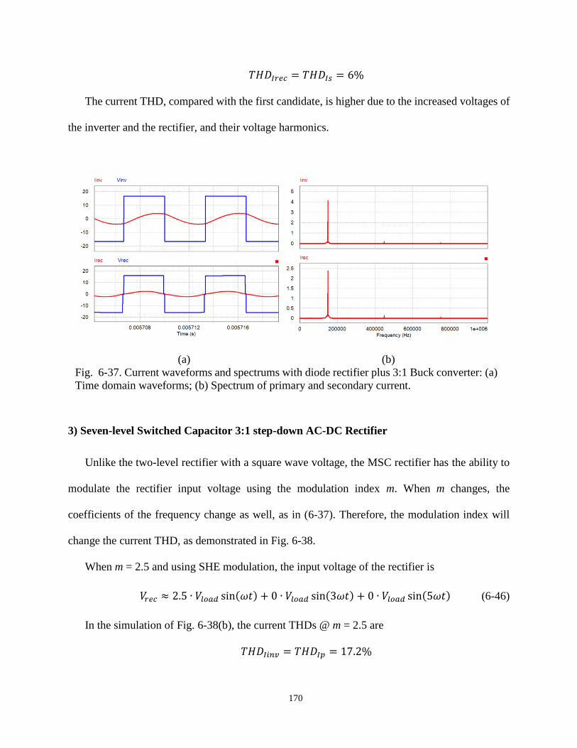
170
𝑇𝐻𝐷𝐼𝑟𝑒𝑐 = 𝑇𝐻𝐷𝐼𝑠 = 6%
The current THD, compared with the first candidate, is higher due to the increased voltages of
the inverter and the rectifier, and their voltage harmonics.
3) Seven-level Switched Capacitor 3:1 step-down AC-DC Rectifier
Unlike the two-level rectifier with a square wave voltage, the MSC rectifier has the ability to
modulate the rectifier input voltage using the modulation index m. When m changes, the
coefficients of the frequency change as well, as in (6-37). Therefore, the modulation index will
change the current THD, as demonstrated in Fig. 6-38.
When m = 2.5 and using SHE modulation, the input voltage of the rectifier is
𝑉𝑟𝑒𝑐 ≈ 2.5 ∙ 𝑉𝑙𝑜𝑎𝑑 sin(𝜔𝑡) + 0 ∙ 𝑉𝑙𝑜𝑎𝑑 sin(3𝜔𝑡) + 0 ∙ 𝑉𝑙𝑜𝑎𝑑 sin(5𝜔𝑡) (6-46)
In the simulation of Fig. 6-38(b), the current THDs @ m = 2.5 are
𝑇𝐻𝐷𝐼𝑖𝑛𝑣 = 𝑇𝐻𝐷𝐼𝑝 = 17.2%
(a) (b)
Fig. 6-37. Current waveforms and spectrums with diode rectifier plus 3:1 Buck converter: (a)
Time domain waveforms; (b) Spectrum of primary and secondary current.
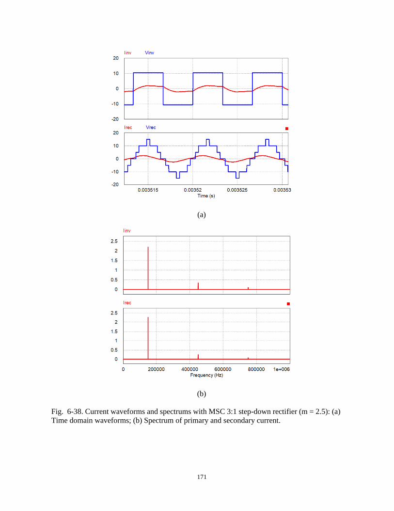
171
(a)
(b)
Fig. 6-38. Current waveforms and spectrums with MSC 3:1 step-down rectifier (m = 2.5): (a)
Time domain waveforms; (b) Spectrum of primary and secondary current.

172
𝑇𝐻𝐷𝐼𝑟𝑒𝑐 = 𝑇𝐻𝐷𝐼𝑠 = 12.3%
However, the current THDs are the same in Fig. 6-37 if the modulation index m changes to
3.81, and the input voltage of the rectifier changes to
𝑉𝑟𝑒𝑐 ≈ 34
𝜋𝑉𝑙𝑜𝑎𝑑 sin(𝜔𝑡) + 3
4
3𝜋𝑉𝑙𝑜𝑎𝑑 sin(3𝜔𝑡) + 3
4
5𝜋𝑉𝑙𝑜𝑎𝑑 sin(5𝜔𝑡) (6-47)
The current THDs with m = 3.81 are
𝑇𝐻𝐷𝐼𝑖𝑛𝑣 = 𝑇𝐻𝐷𝐼𝑝 = 4.7%
𝑇𝐻𝐷𝐼𝑟𝑒𝑐 = 𝑇𝐻𝐷𝐼𝑠 = 6.7%
4) Synchronous Rectifier Plus Switched-Capacitor DC/DC Converter
The waveforms of the fourth candidate are the same in Fig. 6-37, the input voltage of the
rectifier is
𝑉𝑟𝑒𝑐 ≈ 34
𝜋𝑉𝑙𝑜𝑎𝑑 sin(𝜔𝑡) + 3
4
3𝜋𝑉𝑙𝑜𝑎𝑑 sin(3𝜔𝑡) + 3
4
5𝜋𝑉𝑙𝑜𝑎𝑑 sin(5𝜔𝑡) (6-48)
The current THDs are
𝑇𝐻𝐷𝐼𝑖𝑛𝑣 = 𝑇𝐻𝐷𝐼𝑝 = 4.7%
𝑇𝐻𝐷𝐼𝑟𝑒𝑐 = 𝑇𝐻𝐷𝐼𝑠 = 6.7%
In summary, at 5V, 20W output, the current THDs using the diode rectifier is the lowest, and
the current THD using the MSC rectifier is highest (m = 2.5). The second and the fourth candidate
have the same current THD, as well as MSC at its maximum modulation index (m = 3.81). The
performance comparison of the current THD is provided in Table 6-11.
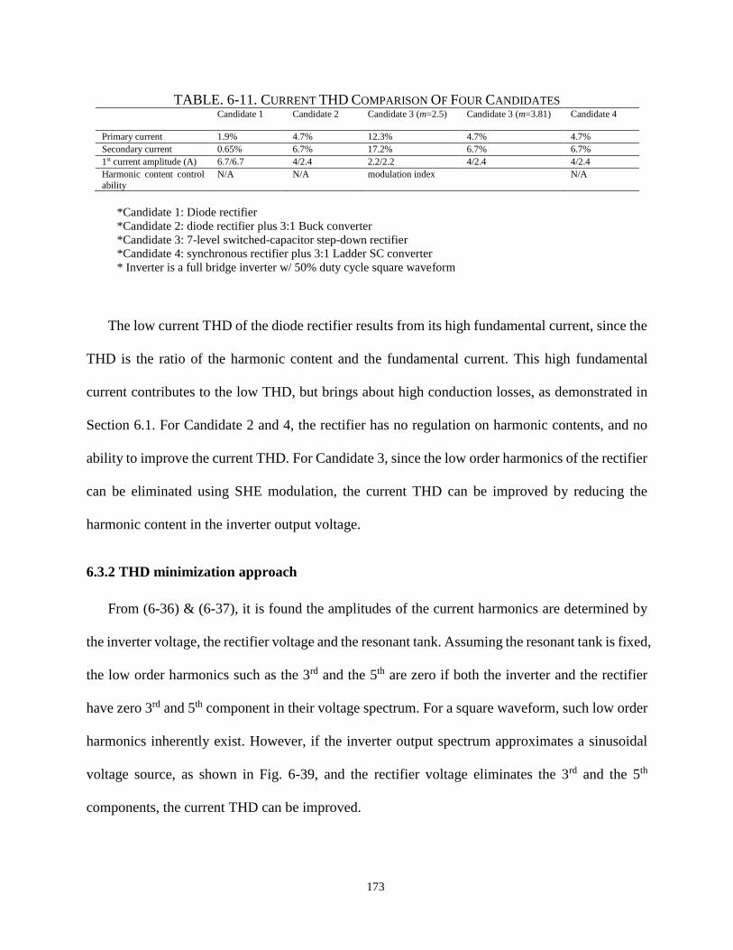
173
The low current THD of the diode rectifier results from its high fundamental current, since the
THD is the ratio of the harmonic content and the fundamental current. This high fundamental
current contributes to the low THD, but brings about high conduction losses, as demonstrated in
Section 6.1. For Candidate 2 and 4, the rectifier has no regulation on harmonic contents, and no
ability to improve the current THD. For Candidate 3, since the low order harmonics of the rectifier
can be eliminated using SHE modulation, the current THD can be improved by reducing the
harmonic content in the inverter output voltage.
6.3.2 THD minimization approach
From (6-36) & (6-37), it is found the amplitudes of the current harmonics are determined by
the inverter voltage, the rectifier voltage and the resonant tank. Assuming the resonant tank is fixed,
the low order harmonics such as the 3rd and the 5th are zero if both the inverter and the rectifier
have zero 3rd and 5th component in their voltage spectrum. For a square waveform, such low order
harmonics inherently exist. However, if the inverter output spectrum approximates a sinusoidal
voltage source, as shown in Fig. 6-39, and the rectifier voltage eliminates the 3rd and the 5th
components, the current THD can be improved.
TABLE. 6-11. CURRENT THD COMPARISON OF FOUR CANDIDATES Candidate 1 Candidate 2 Candidate 3 (m=2.5)
Candidate 3 (m=3.81)
Candidate 4
Primary current 1.9% 4.7% 12.3% 4.7% 4.7%
Secondary current 0.65% 6.7% 17.2% 6.7% 6.7%
1st current amplitude (A) 6.7/6.7 4/2.4 2.2/2.2 4/2.4 4/2.4
Harmonic content control
ability
N/A N/A modulation index N/A
*Candidate 1: Diode rectifier
*Candidate 2: diode rectifier plus 3:1 Buck converter
*Candidate 3: 7-level switched-capacitor step-down rectifier
*Candidate 4: synchronous rectifier plus 3:1 Ladder SC converter
* Inverter is a full bridge inverter w/ 50% duty cycle square waveform
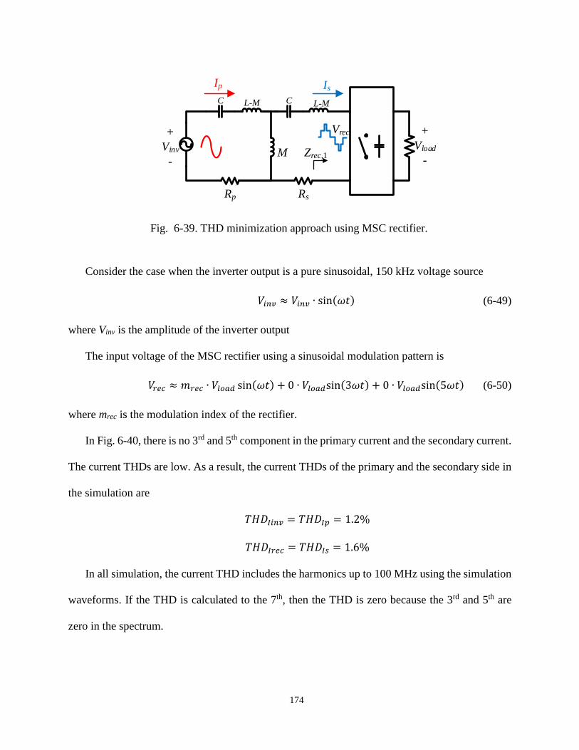
174
Consider the case when the inverter output is a pure sinusoidal, 150 kHz voltage source
𝑉𝑖𝑛𝑣 ≈ 𝑉𝑖𝑛𝑣 ∙ sin(𝜔𝑡) (6-49)
where Vinv is the amplitude of the inverter output
The input voltage of the MSC rectifier using a sinusoidal modulation pattern is
𝑉𝑟𝑒𝑐 ≈ 𝑚𝑟𝑒𝑐 ∙ 𝑉𝑙𝑜𝑎𝑑 sin(𝜔𝑡) + 0 ∙ 𝑉𝑙𝑜𝑎𝑑sin(3𝜔𝑡) + 0 ∙ 𝑉𝑙𝑜𝑎𝑑sin(5𝜔𝑡) (6-50)
where mrec is the modulation index of the rectifier.
In Fig. 6-40, there is no 3rd and 5th component in the primary current and the secondary current.
The current THDs are low. As a result, the current THDs of the primary and the secondary side in
the simulation are
𝑇𝐻𝐷𝐼𝑖𝑛𝑣 = 𝑇𝐻𝐷𝐼𝑝 = 1.2%
𝑇𝐻𝐷𝐼𝑟𝑒𝑐 = 𝑇𝐻𝐷𝐼𝑠 = 1.6%
In all simulation, the current THD includes the harmonics up to 100 MHz using the simulation
waveforms. If the THD is calculated to the 7th, then the THD is zero because the 3rd and 5th are
zero in the spectrum.
C L-M L-MC
M
Vrec+
Vinv
-
+
Vload
-
Ip Is
Zrec,1
Rp Rs
Fig. 6-39. THD minimization approach using MSC rectifier.
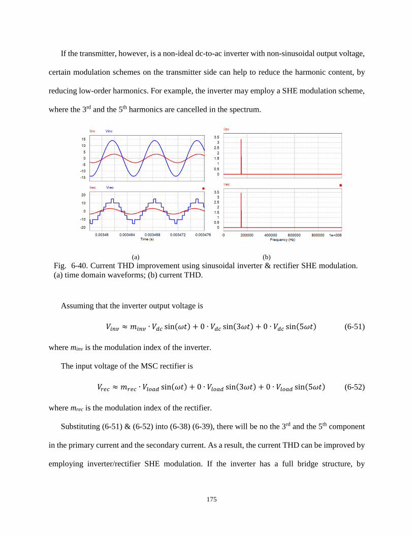
175
If the transmitter, however, is a non-ideal dc-to-ac inverter with non-sinusoidal output voltage,
certain modulation schemes on the transmitter side can help to reduce the harmonic content, by
reducing low-order harmonics. For example, the inverter may employ a SHE modulation scheme,
where the 3rd and the 5th harmonics are cancelled in the spectrum.
Assuming that the inverter output voltage is
𝑉𝑖𝑛𝑣 ≈ 𝑚𝑖𝑛𝑣 ∙ 𝑉𝑑𝑐 sin(𝜔𝑡) + 0 ∙ 𝑉𝑑𝑐 sin(3𝜔𝑡) + 0 ∙ 𝑉𝑑𝑐 sin(5𝜔𝑡) (6-51)
where minv is the modulation index of the inverter.
The input voltage of the MSC rectifier is
𝑉𝑟𝑒𝑐 ≈ 𝑚𝑟𝑒𝑐 ∙ 𝑉𝑙𝑜𝑎𝑑 sin(𝜔𝑡) + 0 ∙ 𝑉𝑙𝑜𝑎𝑑 sin(3𝜔𝑡) + 0 ∙ 𝑉𝑙𝑜𝑎𝑑 sin(5𝜔𝑡) (6-52)
where mrec is the modulation index of the rectifier.
Substituting (6-51) & (6-52) into (6-38) (6-39), there will be no the 3rd and the 5th component
in the primary current and the secondary current. As a result, the current THD can be improved by
employing inverter/rectifier SHE modulation. If the inverter has a full bridge structure, by
(a) (b)
Fig. 6-40. Current THD improvement using sinusoidal inverter & rectifier SHE modulation.
(a) time domain waveforms; (b) current THD.
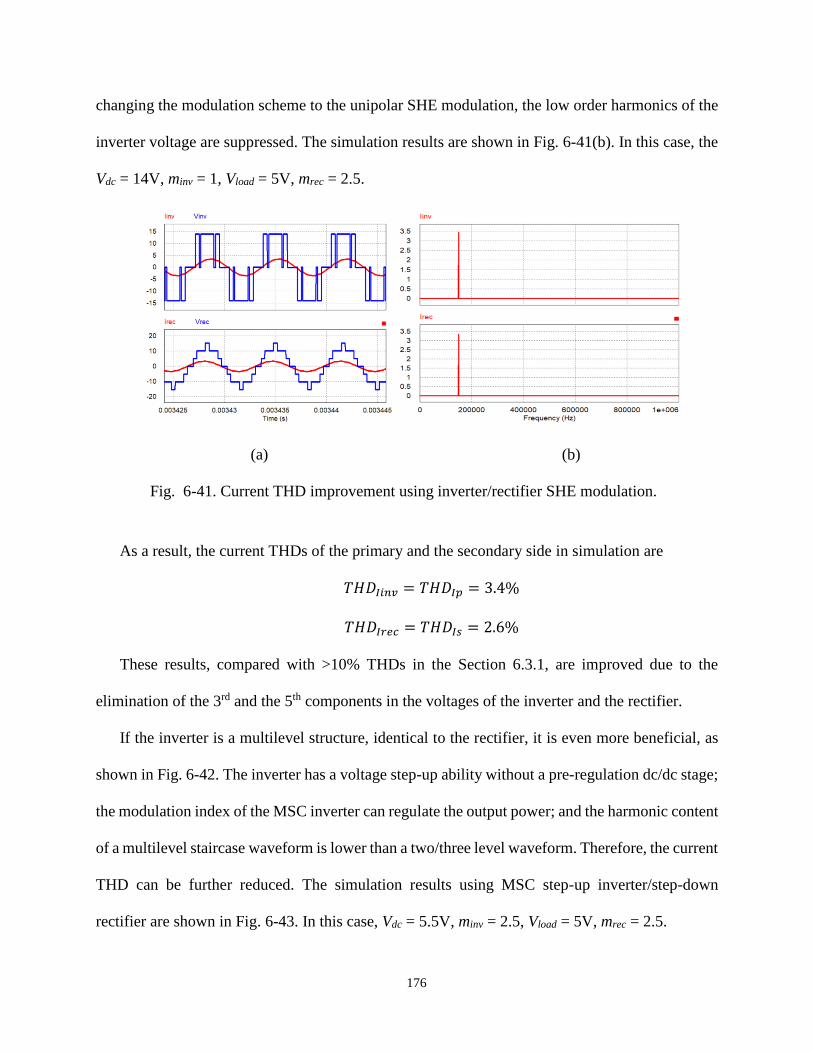
176
changing the modulation scheme to the unipolar SHE modulation, the low order harmonics of the
inverter voltage are suppressed. The simulation results are shown in Fig. 6-41(b). In this case, the
Vdc = 14V, minv = 1, Vload = 5V, mrec = 2.5.
As a result, the current THDs of the primary and the secondary side in simulation are
𝑇𝐻𝐷𝐼𝑖𝑛𝑣 = 𝑇𝐻𝐷𝐼𝑝 = 3.4%
𝑇𝐻𝐷𝐼𝑟𝑒𝑐 = 𝑇𝐻𝐷𝐼𝑠 = 2.6%
These results, compared with >10% THDs in the Section 6.3.1, are improved due to the
elimination of the 3rd and the 5th components in the voltages of the inverter and the rectifier.
If the inverter is a multilevel structure, identical to the rectifier, it is even more beneficial, as
shown in Fig. 6-42. The inverter has a voltage step-up ability without a pre-regulation dc/dc stage;
the modulation index of the MSC inverter can regulate the output power; and the harmonic content
of a multilevel staircase waveform is lower than a two/three level waveform. Therefore, the current
THD can be further reduced. The simulation results using MSC step-up inverter/step-down
rectifier are shown in Fig. 6-43. In this case, Vdc = 5.5V, minv = 2.5, Vload = 5V, mrec = 2.5.
(a) (b)
Fig. 6-41. Current THD improvement using inverter/rectifier SHE modulation.
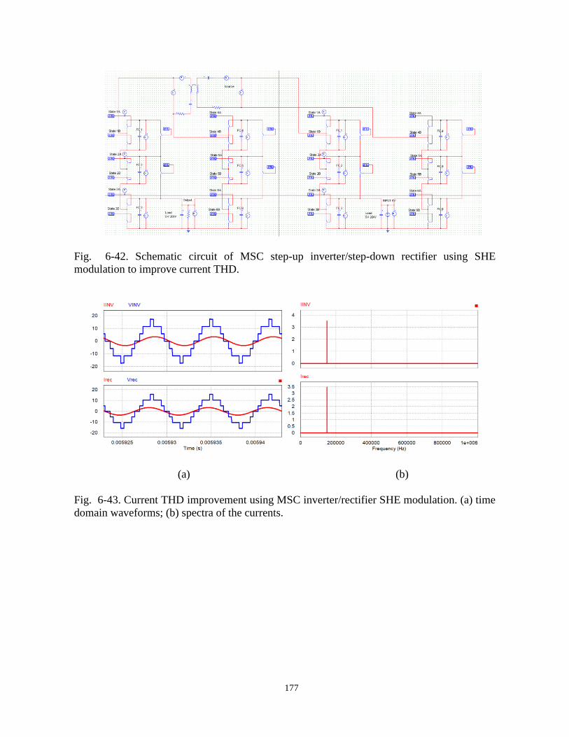
177
Fig. 6-42. Schematic circuit of MSC step-up inverter/step-down rectifier using SHE
modulation to improve current THD.
(a) (b)
Fig. 6-43. Current THD improvement using MSC inverter/rectifier SHE modulation. (a) time
domain waveforms; (b) spectra of the currents.
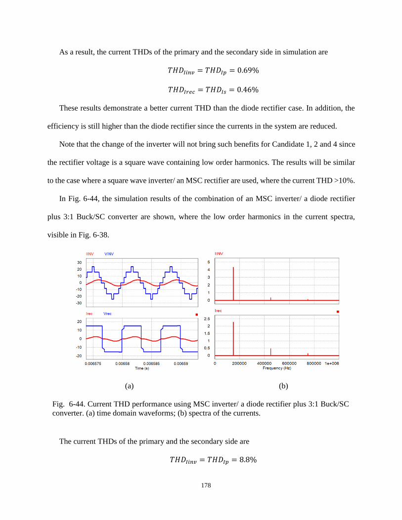
178
As a result, the current THDs of the primary and the secondary side in simulation are
𝑇𝐻𝐷𝐼𝑖𝑛𝑣 = 𝑇𝐻𝐷𝐼𝑝 = 0.69%
𝑇𝐻𝐷𝐼𝑟𝑒𝑐 = 𝑇𝐻𝐷𝐼𝑠 = 0.46%
These results demonstrate a better current THD than the diode rectifier case. In addition, the
efficiency is still higher than the diode rectifier since the currents in the system are reduced.
Note that the change of the inverter will not bring such benefits for Candidate 1, 2 and 4 since
the rectifier voltage is a square wave containing low order harmonics. The results will be similar
to the case where a square wave inverter/ an MSC rectifier are used, where the current THD >10%.
In Fig. 6-44, the simulation results of the combination of an MSC inverter/ a diode rectifier
plus 3:1 Buck/SC converter are shown, where the low order harmonics in the current spectra,
visible in Fig. 6-38.
The current THDs of the primary and the secondary side are
𝑇𝐻𝐷𝐼𝑖𝑛𝑣 = 𝑇𝐻𝐷𝐼𝑝 = 8.8%
(a) (b)
Fig. 6-44. Current THD performance using MSC inverter/ a diode rectifier plus 3:1 Buck/SC
converter. (a) time domain waveforms; (b) spectra of the currents.
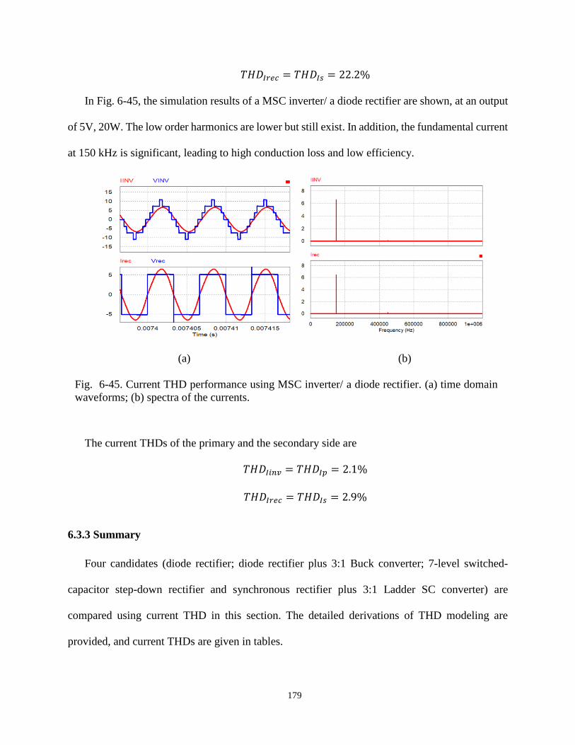
179
𝑇𝐻𝐷𝐼𝑟𝑒𝑐 = 𝑇𝐻𝐷𝐼𝑠 = 22.2%
In Fig. 6-45, the simulation results of a MSC inverter/ a diode rectifier are shown, at an output
of 5V, 20W. The low order harmonics are lower but still exist. In addition, the fundamental current
at 150 kHz is significant, leading to high conduction loss and low efficiency.
The current THDs of the primary and the secondary side are
𝑇𝐻𝐷𝐼𝑖𝑛𝑣 = 𝑇𝐻𝐷𝐼𝑝 = 2.1%
𝑇𝐻𝐷𝐼𝑟𝑒𝑐 = 𝑇𝐻𝐷𝐼𝑠 = 2.9%
6.3.3 Summary
Four candidates (diode rectifier; diode rectifier plus 3:1 Buck converter; 7-level switched-
capacitor step-down rectifier and synchronous rectifier plus 3:1 Ladder SC converter) are
compared using current THD in this section. The detailed derivations of THD modeling are
provided, and current THDs are given in tables.
(a) (b)
Fig. 6-45. Current THD performance using MSC inverter/ a diode rectifier. (a) time domain
waveforms; (b) spectra of the currents.
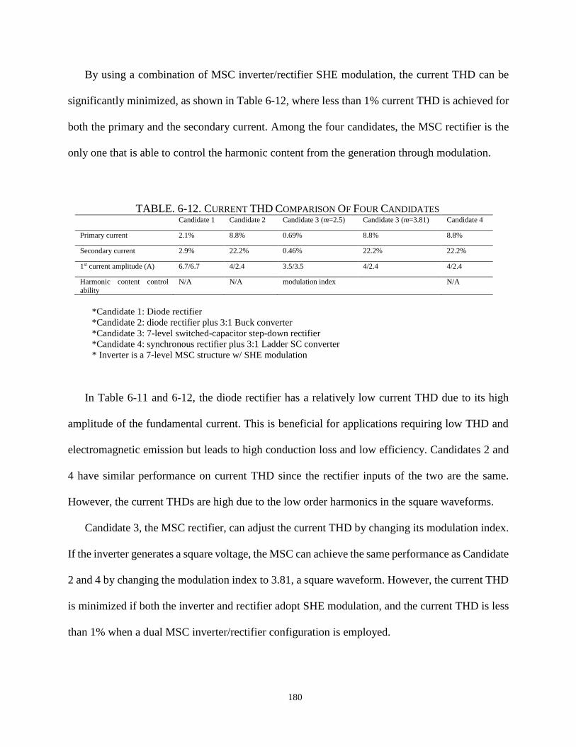
180
By using a combination of MSC inverter/rectifier SHE modulation, the current THD can be
significantly minimized, as shown in Table 6-12, where less than 1% current THD is achieved for
both the primary and the secondary current. Among the four candidates, the MSC rectifier is the
only one that is able to control the harmonic content from the generation through modulation.
In Table 6-11 and 6-12, the diode rectifier has a relatively low current THD due to its high
amplitude of the fundamental current. This is beneficial for applications requiring low THD and
electromagnetic emission but leads to high conduction loss and low efficiency. Candidates 2 and
4 have similar performance on current THD since the rectifier inputs of the two are the same.
However, the current THDs are high due to the low order harmonics in the square waveforms.
Candidate 3, the MSC rectifier, can adjust the current THD by changing its modulation index.
If the inverter generates a square voltage, the MSC can achieve the same performance as Candidate
2 and 4 by changing the modulation index to 3.81, a square waveform. However, the current THD
is minimized if both the inverter and rectifier adopt SHE modulation, and the current THD is less
than 1% when a dual MSC inverter/rectifier configuration is employed.
TABLE. 6-12. CURRENT THD COMPARISON OF FOUR CANDIDATES Candidate 1 Candidate 2 Candidate 3 (m=2.5) Candidate 3 (m=3.81) Candidate 4
Primary current 2.1% 8.8% 0.69% 8.8% 8.8%
Secondary current 2.9% 22.2% 0.46% 22.2% 22.2%
1st current amplitude (A) 6.7/6.7 4/2.4 3.5/3.5 4/2.4 4/2.4
Harmonic content control
ability
N/A N/A modulation index N/A
*Candidate 1: Diode rectifier
*Candidate 2: diode rectifier plus 3:1 Buck converter
*Candidate 3: 7-level switched-capacitor step-down rectifier
*Candidate 4: synchronous rectifier plus 3:1 Ladder SC converter
* Inverter is a 7-level MSC structure w/ SHE modulation

181
6.4 Volume Estimation
To estimate the total volume of each candidate, some assumptions are made. 1) The 5V
semiconductor device (diode and transistor) has a base area 1. Since the device area is proportional
to the voltage rating, a 15V device has an area 3*1. 2) Using commercial ceramic capacitor as a
reference, a 5V, 20 µF capacitor has a volume base 1 (1 x 0.5 x 0.5 mm, 0402 package). A 15V,
20µF capacitor has a volume 10*1 (2 x 1.25 x 1 mm, 0805 package). 3) For the two stage
candidates, SR rectifier plus Buck converter and SR rectifier plus SC converter, a 15V, 100 µF dc
bus capacitor is needed as an energy buffer. 4) A 5V, 40 µF dc output capacitor is employed for
candidates 2, 3 and 4. The diode rectifier has a larger output capacitance to achieve similar output
voltage ripple due to excessive input current. 5) The driver circuit, control circuit and auxiliary
circuit are not included in this volume estimation. The total topology volume is defined
Total volume = Device area + Passive component
1) Diode rectifier
Four 5V diodes are needed for the diode rectifier. The passive component in the diode rectifier
is the output capacitor. Since the input current amplitude of the diode rectifier is nearly twice in
other candidates, a 5V, 100 µF dc output capacitor is employed to achieve similar output voltage
ripple.
The total volume of the diode rectifier is
𝑉𝑐𝑎𝑛𝑑1 = (4 ∙ 1) + (5 ∙ 1)
2) SR rectifier plus 3:1 Buck converter
A total four 15 V transistor is required for SR rectifier and two 15 V transistors for 3:1 Buck
converter. The dc bus capacitor is 15 V, 100 µF. According the commercial Buck converter
182
datasheet, one inductor for 3:1 Buck converter is used, and is estimated as 470nH, 2.7 x 2.2 x 1.2
mm = 28 * 0402 capacitor.
The total volume of the SR rectifier plus 3:1 Buck converter is
𝑉𝑐𝑎𝑛𝑑2 = (4 ∙ 3 + 2 ∙ 3) + (5 ∙ 1 ∙ 10 + 28 + 2) = 18 + 80
3) 7-level switched-capacitor step-down rectifier
For a seven-level SC rectifier, a total of sixteen 5V MOSFETs are needed. The passive
components include six 5V ceramic capacitor (est. 40 µF/ea.).
The total volume of 7-level SC rectifier is
𝑉𝑐𝑎𝑛𝑑3 = (16 ∙ 1) + (6 ∙ 2 + 2) = 16 + 14
4) SR rectifier plus 3:1 Ladder SC converter
The fourth candidate requires four 15V transistor in the SR rectifier stage, and six 5V
transistors in the 3:1 Ladder SC converter. The passive components include one 15 V DC capacitor
(est. 100 µF) and three 5V DC capacitor (est. 40 µF/ea.)
The total volume of the SR rectifier plus 3:1 SC converter is
𝑉𝑐𝑎𝑛𝑑4 = (4 ∙ 3 + 6 ∙ 1) × (5 ∙ 1 ∙ 10 + 3 ∙ 2 + 2) = 18 + 58
The total volume of each candidate is given in Table 6-13. The candidate 2 is the largest among
the four due to its dc bus capacitor and bulky magnetic component. Note that the sample inductor
is for 12 W application, and the size could be different for final 20 W application. The proposed
MSC rectifier has a reduced passive component volume due to low voltage rating of flying
capacitors. In addition, there is no need for a high-voltage rating dc bus capacitor for this one-stage
ac-dc rectifier. The MSC rectifier can also achieve voltage step-down conversion without magnetic
component, further improving power density.
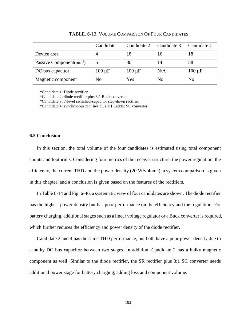
183
6.5 Conclusion
In this section, the total volume of the four candidates is estimated using total component
counts and footprints. Considering four metrics of the receiver structure: the power regulation, the
efficiency, the current THD and the power density (20 W/volume), a system comparison is given
in this chapter, and a conclusion is given based on the features of the rectifiers.
In Table 6-14 and Fig. 6-46, a systematic view of four candidates are shown. The diode rectifier
has the highest power density but has poor performance on the efficiency and the regulation. For
battery charging, additional stages such as a linear voltage regulator or a Buck converter is required,
which further reduces the efficiency and power density of the diode rectifier.
Candidate 2 and 4 has the same THD performance, but both have a poor power density due to
a bulky DC bus capacitor between two stages. In addition, Candidate 2 has a bulky magnetic
component as well. Similar to the diode rectifier, the SR rectifier plus 3:1 SC converter needs
additional power stage for battery charging, adding loss and component volume.
TABLE. 6-13. VOLUME COMPARISON OF FOUR CANDIDATES
Candidate 1 Candidate 2 Candidate 3 Candidate 4
Device area 4 18 16 18
Passive Component(mm3) 5 80 14 58
DC bus capacitor 100 µF 100 µF N/A 100 µF
Magnetic component No Yes No No
*Candidate 1: Diode rectifier
*Candidate 2: diode rectifier plus 3:1 Buck converter
*Candidate 3: 7-level switched-capacitor step-down rectifier
*Candidate 4: synchronous rectifier plus 3:1 Ladder SC converter
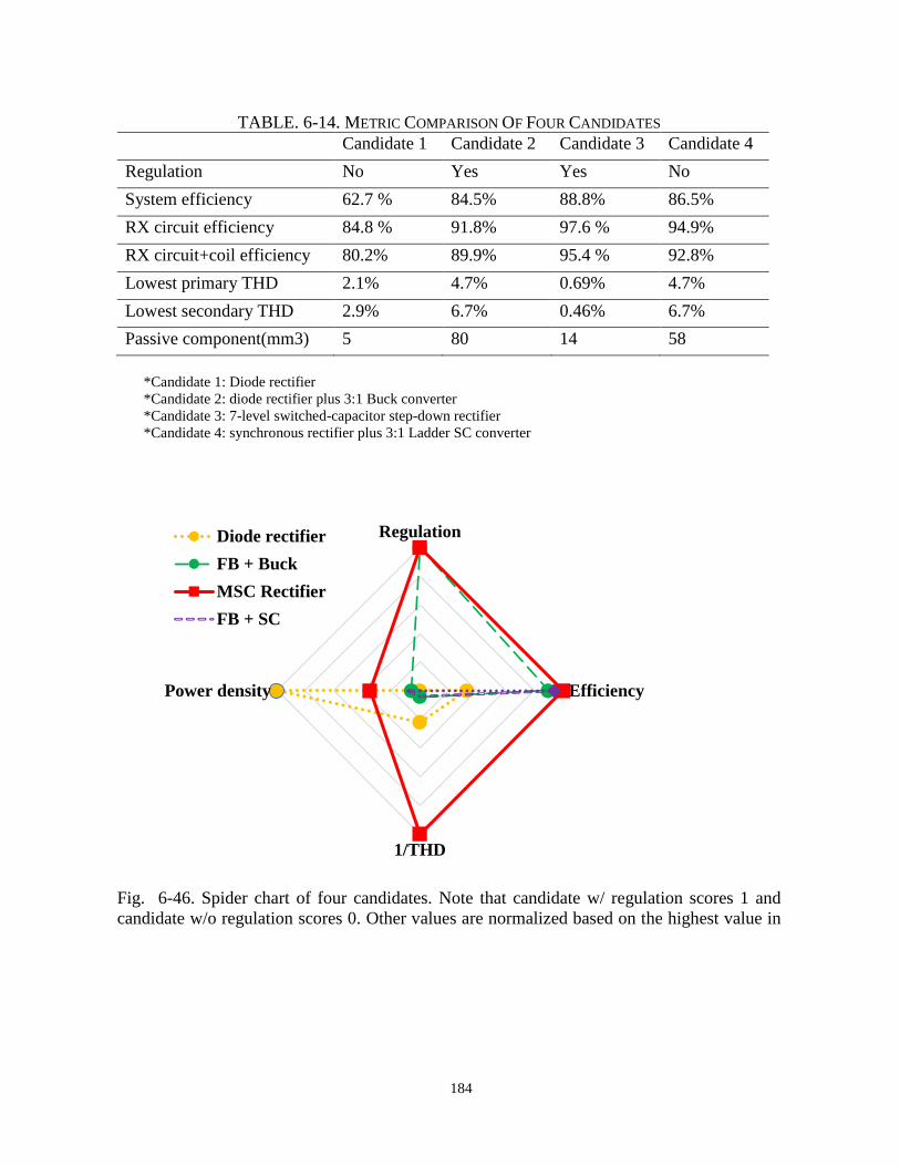
184
TABLE. 6-14. METRIC COMPARISON OF FOUR CANDIDATES
Candidate 1 Candidate 2 Candidate 3 Candidate 4
Regulation No Yes Yes No
System efficiency 62.7 % 84.5% 88.8% 86.5%
RX circuit efficiency 84.8 % 91.8% 97.6 % 94.9%
RX circuit+coil efficiency 80.2% 89.9% 95.4 % 92.8%
Lowest primary THD 2.1% 4.7% 0.69% 4.7%
Lowest secondary THD 2.9% 6.7% 0.46% 6.7%
Passive component(mm3) 5 80 14 58
*Candidate 1: Diode rectifier
*Candidate 2: diode rectifier plus 3:1 Buck converter
*Candidate 3: 7-level switched-capacitor step-down rectifier
*Candidate 4: synchronous rectifier plus 3:1 Ladder SC converter
Fig. 6-46. Spider chart of four candidates. Note that candidate w/ regulation scores 1 and
candidate w/o regulation scores 0. Other values are normalized based on the highest value in
the item.
Regulation
Efficiency
1/THD
Power density
Diode rectifier
FB + Buck
MSC Rectifier
FB + SC
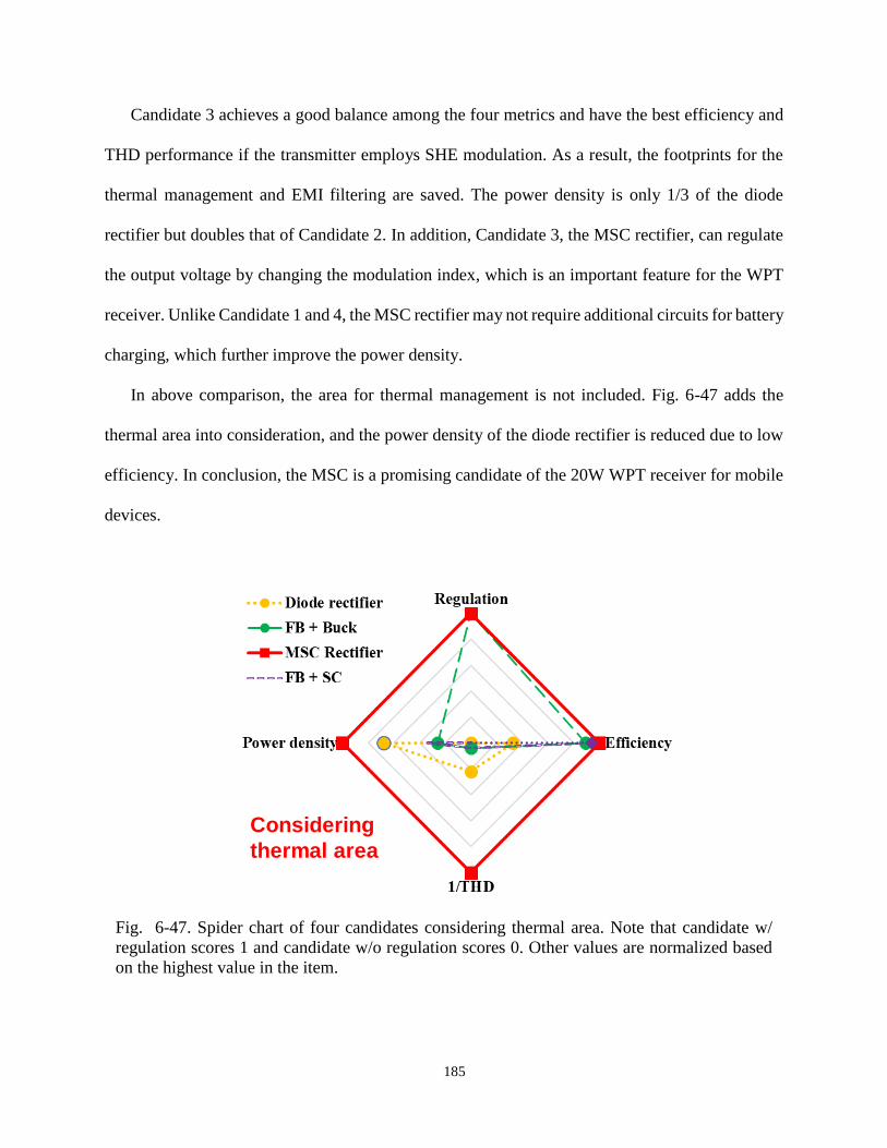
185
Candidate 3 achieves a good balance among the four metrics and have the best efficiency and
THD performance if the transmitter employs SHE modulation. As a result, the footprints for the
thermal management and EMI filtering are saved. The power density is only 1/3 of the diode
rectifier but doubles that of Candidate 2. In addition, Candidate 3, the MSC rectifier, can regulate
the output voltage by changing the modulation index, which is an important feature for the WPT
receiver. Unlike Candidate 1 and 4, the MSC rectifier may not require additional circuits for battery
charging, which further improve the power density.
In above comparison, the area for thermal management is not included. Fig. 6-47 adds the
thermal area into consideration, and the power density of the diode rectifier is reduced due to low
efficiency. In conclusion, the MSC is a promising candidate of the 20W WPT receiver for mobile
devices.
Fig. 6-47. Spider chart of four candidates considering thermal area. Note that candidate w/
regulation scores 1 and candidate w/o regulation scores 0. Other values are normalized based
on the highest value in the item.
Considering
thermal area

186
7. Design and Implementation of MSC Rectifier
7.1 Device Sizing for Integrated Circuit Design
Four candidates are reviewed in the previous chapter, and their advantages/disadvantages are
shown by comparisons of the regulation, efficiency, current THD and volume. Among the four
candidates, the diode rectifier is not suitable for 20W wireless fast charging due to excessive
conduction loss and low efficiency. The diode rectifier plus a Buck converter can achieve high
efficiency but has poor power density. Space on the mobile devices is important, and therefore
Candidates 1 and 2 are not suitable due to bulky magnetic components and extensive thermal
dissipation area. Thanks to a high-power density design using the switched-capacitor circuits,
candidates 3 and 4 show promise for an integrated circuit prototype.
In this chapter, a detailed procedure for sizing device for integrated circuit (IC) design is
demonstrated and design examples are included. Several parameters of the IC process are provided
for the low-voltage switching devices. The flying capacitors are pre-selected at 20µF, 10V. With
this capacitor rating, a small 0402 package can save space, and the capacitance ensure a low charge
sharing loss in SSL region. The system parameters are given in Table 7-1. The output is a 9V, 20W
resistive load. For the selection of the device process, the voltage margin is picked at 30%, e.g.
using 12 V device process for a 9V drain-to-source voltage.
TABLE. 7-1.SYSTEM DESIGN PARAMETERS
Item Parameter
Flying capacitor Cfly 20 µF
Output capacitor 100 µF(opt)
DC bus capacitor N/A
Input current frequency fs 150 kHz
Load voltage Vload 9V
Output power 20 W
Device voltage margin 30%
187
7.1.1 5 level SC Rectifier
In the simulation circuit, the input of the rectifier is simplified as a sinusoidal current source
whose frequency is 150 kHz, and the amplitude is set to achieve a 9V, 20W output. The flying
capacitors are 20 µF, with four capacitors in total. For the 5 level, 2:1 step-down SC rectifier, the
output voltage, and the flying capacitor voltages are clamped at 9V so the switching devices are
rated at 12V to maintain a 30% voltage margin. The input current and voltage waveforms of the
rectifier are given in Fig. 7-1(a), and one flying capacitor voltage and the output voltage are given
in Fig. 7-1(b).
Assuming the device area is A12 for the 12V process, then the device parameters are
𝑇𝑟𝑎𝑛𝑠𝑖𝑠𝑡𝑜𝑟 𝑅𝑒𝑠𝑖𝑠𝑡𝑎𝑛𝑐𝑒 = 𝑅𝑑𝑠12 𝑚Ω/𝐴12(𝑚𝑚2) (7-1)
𝑇𝑟𝑎𝑛𝑠𝑖𝑠𝑡𝑜𝑟 𝑔𝑎𝑡𝑒 𝑐ℎ𝑎𝑟𝑔𝑒 = 𝑄𝑔𝑠12 𝑛𝐶 ∙ 𝐴12(𝑚𝑚2) (7-2)
𝑇𝑟𝑎𝑛𝑠𝑖𝑠𝑡𝑜𝑟 𝑜𝑢𝑡𝑝𝑢𝑡 𝑐ℎ𝑎𝑟𝑔𝑒 = 𝑄𝑜𝑠𝑠12 𝑝𝐶 ∙ 𝐴12(𝑚𝑚2) (7-3)
The loss mechanisms of the multilevel SC rectifier are investigated in Chapter 6.3. This
includes gate charge loss, output capacitance charge loss, conduction loss and charge sharing loss.
The equations to calculate losses are modified for normalized devices as follows
The gate charge loss of one switching device is
𝑃𝑔𝑠 = 𝑉𝑔𝑠 ∙ 𝑄𝑔𝑠12 ∙ 𝑓𝑠 (7-4)
where the gate-to-source voltage is assumed Vgs = 5V, and fs = 150 kHz.
The output capacitance charge loss of one switching device is
𝑃𝑐𝑜𝑠𝑠 = 𝑉𝑙𝑜𝑎𝑑 ∙ 𝑄𝑜𝑠𝑠12 ∙ 𝑓𝑠 (7-5)
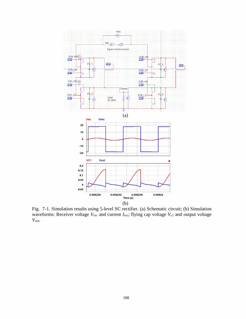
188
(a)
(b)
Fig. 7-1. Simulation results using 5-level SC rectifier. (a) Schematic circuit; (b) Simulation
waveforms: Receiver voltage Vrec and current Irec; flying cap voltage Vc1 and output voltage
Vout.
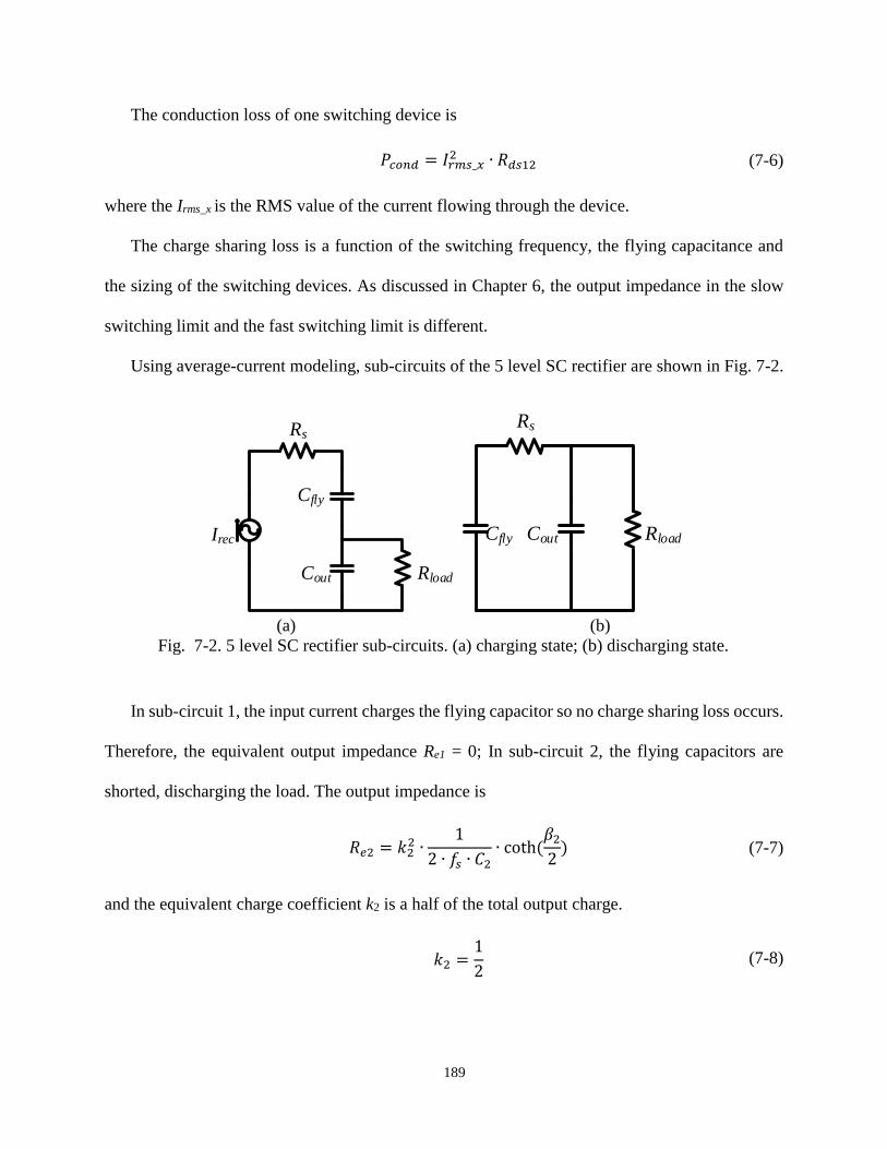
189
The conduction loss of one switching device is
𝑃𝑐𝑜𝑛𝑑 = 𝐼𝑟𝑚𝑠_𝑥2 ∙ 𝑅𝑑𝑠12 (7-6)
where the Irms_x is the RMS value of the current flowing through the device.
The charge sharing loss is a function of the switching frequency, the flying capacitance and
the sizing of the switching devices. As discussed in Chapter 6, the output impedance in the slow
switching limit and the fast switching limit is different.
Using average-current modeling, sub-circuits of the 5 level SC rectifier are shown in Fig. 7-2.
In sub-circuit 1, the input current charges the flying capacitor so no charge sharing loss occurs.
Therefore, the equivalent output impedance Re1 = 0; In sub-circuit 2, the flying capacitors are
shorted, discharging the load. The output impedance is
𝑅𝑒2 = 𝑘22 ∙
1
2 ∙ 𝑓𝑠 ∙ 𝐶2∙ coth (
𝛽2
2) (7-7)
and the equivalent charge coefficient k2 is a half of the total output charge.
𝑘2 =1
2 (7-8)
(a) (b)
Fig. 7-2. 5 level SC rectifier sub-circuits. (a) charging state; (b) discharging state.
Irec
Cfly
RloadCout
Rs
Cfly RloadCout
Rs
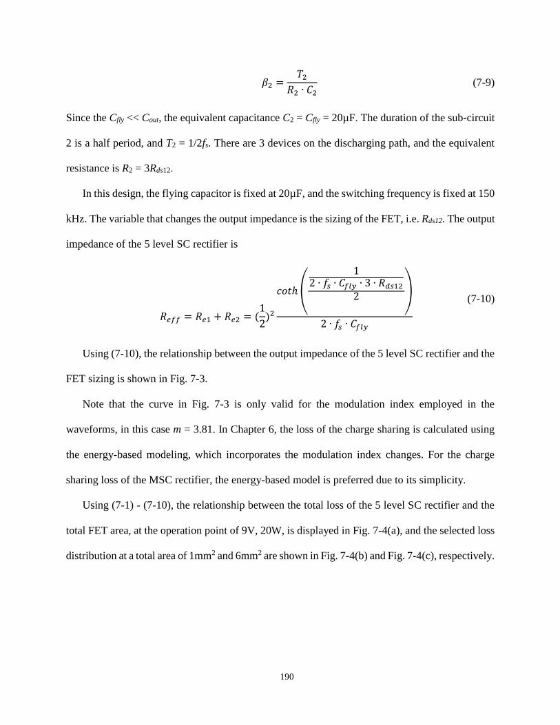
190
𝛽2 =𝑇2
𝑅2 ∙ 𝐶2 (7-9)
Since the Cfly << Cout, the equivalent capacitance C2 = Cfly = 20µF. The duration of the sub-circuit
2 is a half period, and T2 = 1/2fs. There are 3 devices on the discharging path, and the equivalent
resistance is R2 = 3Rds12.
In this design, the flying capacitor is fixed at 20µF, and the switching frequency is fixed at 150
kHz. The variable that changes the output impedance is the sizing of the FET, i.e. Rds12. The output
impedance of the 5 level SC rectifier is
𝑅𝑒𝑓𝑓 = 𝑅𝑒1 + 𝑅𝑒2 = (1
2)2
𝑐𝑜𝑡ℎ (
12 ∙ 𝑓𝑠 ∙ 𝐶𝑓𝑙𝑦 ∙ 3 ∙ 𝑅𝑑𝑠12
2 )
2 ∙ 𝑓𝑠 ∙ 𝐶𝑓𝑙𝑦
(7-10)
Using (7-10), the relationship between the output impedance of the 5 level SC rectifier and the
FET sizing is shown in Fig. 7-3.
Note that the curve in Fig. 7-3 is only valid for the modulation index employed in the
waveforms, in this case m = 3.81. In Chapter 6, the loss of the charge sharing is calculated using
the energy-based modeling, which incorporates the modulation index changes. For the charge
sharing loss of the MSC rectifier, the energy-based model is preferred due to its simplicity.
Using (7-1) - (7-10), the relationship between the total loss of the 5 level SC rectifier and the
total FET area, at the operation point of 9V, 20W, is displayed in Fig. 7-4(a), and the selected loss
distribution at a total area of 1mm2 and 6mm2 are shown in Fig. 7-4(b) and Fig. 7-4(c), respectively.
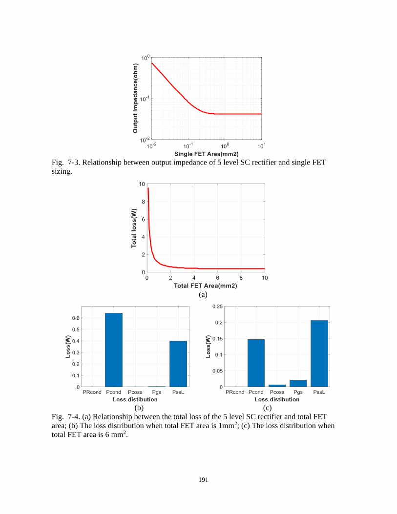
191
Fig. 7-3. Relationship between output impedance of 5 level SC rectifier and single FET
sizing.
(a)
(b) (c)
Fig. 7-4. (a) Relationship between the total loss of the 5 level SC rectifier and total FET
area; (b) The loss distribution when total FET area is 1mm2; (c) The loss distribution when
total FET area is 6 mm2.
192
In this design, the FET sizing the control variable. It is found that the circuit operates in the
SSL region when the total area reaches 4 mm2, and further increasing the FET area does not
significantly improve the efficiency. When the total FET area is less than 2 mm2, the circuit
operates in the FSL, where the 20µF flying capacitors are not fully utilized. As a result, the
capacitance should be re-sized so that the total volume is further reduced, without significant
reduction in efficiency.
7.1.2 Synchronous Rectifier plus 2:1 SC converter
In the simulation circuit, the input of the rectifier is again a sinusoidal current source whose
frequency is 150 kHz, and whose amplitude is adjusted to obtain a 9V, 20W output. The flying
capacitor is 40 µF, i.e. two 20 µF capacitors in parallel. Therefore, the total number of capacitors
is the same as in the 5 level SC rectifier.
For the synchronous rectifier plus 2:1 step-down SC converter, the input voltage is 18V and
the flying capacitor voltages are clamped at 9V. Therefore, two 12V devices in series are used for
each switch to maintain a 30% voltage margin at the rectifier stage. The 2:1 SC converter uses
12V device. The input current and voltage waveforms of the rectifier are given in Fig. 7-5(a), and
one flying capacitor voltage and the output voltage are given in Fig. 7-5(b).
The loss mechanisms of the synchronous rectifier plus 2:1 step-down SC converter are
investigated in Section 6.2, which includes gate charge loss, output capacitance charge loss,
conduction loss and charge sharing loss. The equation to calculate those losses are (7-4) – (7-6).
Using the average-current modeling, sub-circuits of the 2:1 step-down SC rectifier is shown in
Fig. 7-6.
In sub-circuit 1, the input voltage charges the flying capacitor, and the equivalent output
impedance is
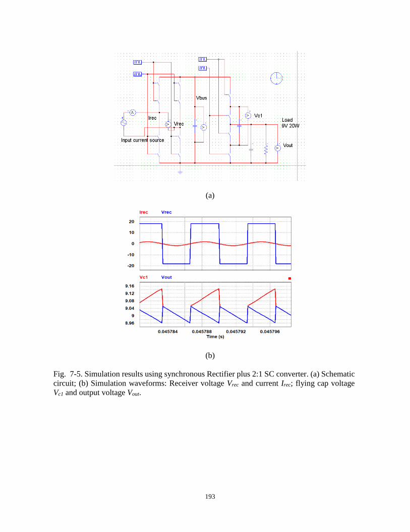
193
(a)
(b)
Fig. 7-5. Simulation results using synchronous Rectifier plus 2:1 SC converter. (a) Schematic
circuit; (b) Simulation waveforms: Receiver voltage Vrec and current Irec; flying cap voltage
Vc1 and output voltage Vout.
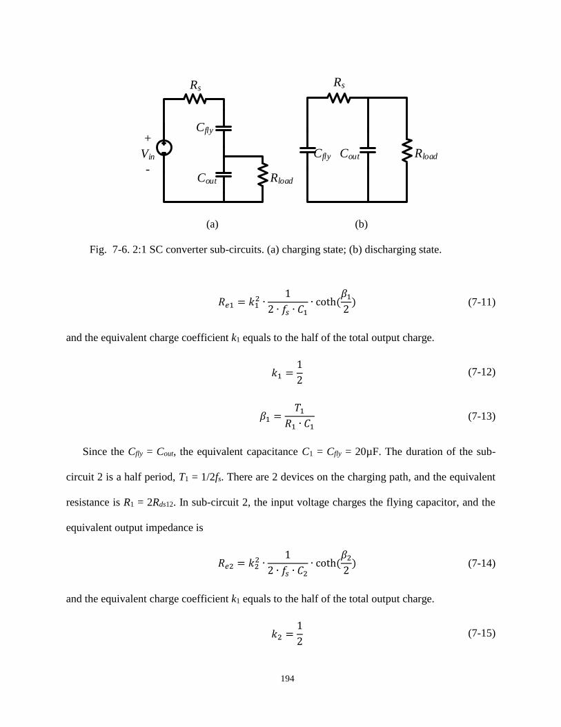
194
𝑅𝑒1 = 𝑘12 ∙
1
2 ∙ 𝑓𝑠 ∙ 𝐶1∙ coth (
𝛽1
2) (7-11)
and the equivalent charge coefficient k1 equals to the half of the total output charge.
𝑘1 =1
2 (7-12)
𝛽1 =𝑇1
𝑅1 ∙ 𝐶1 (7-13)
Since the Cfly = Cout, the equivalent capacitance C1 = Cfly = 20µF. The duration of the sub-
circuit 2 is a half period, T1 = 1/2fs. There are 2 devices on the charging path, and the equivalent
resistance is R1 = 2Rds12. In sub-circuit 2, the input voltage charges the flying capacitor, and the
equivalent output impedance is
𝑅𝑒2 = 𝑘22 ∙
1
2 ∙ 𝑓𝑠 ∙ 𝐶2∙ coth (
𝛽2
2) (7-14)
and the equivalent charge coefficient k1 equals to the half of the total output charge.
𝑘2 =1
2 (7-15)
(a) (b)
Fig. 7-6. 2:1 SC converter sub-circuits. (a) charging state; (b) discharging state.
Cfly+
Vin
-RloadCout
Rs
Cfly RloadCout
Rs
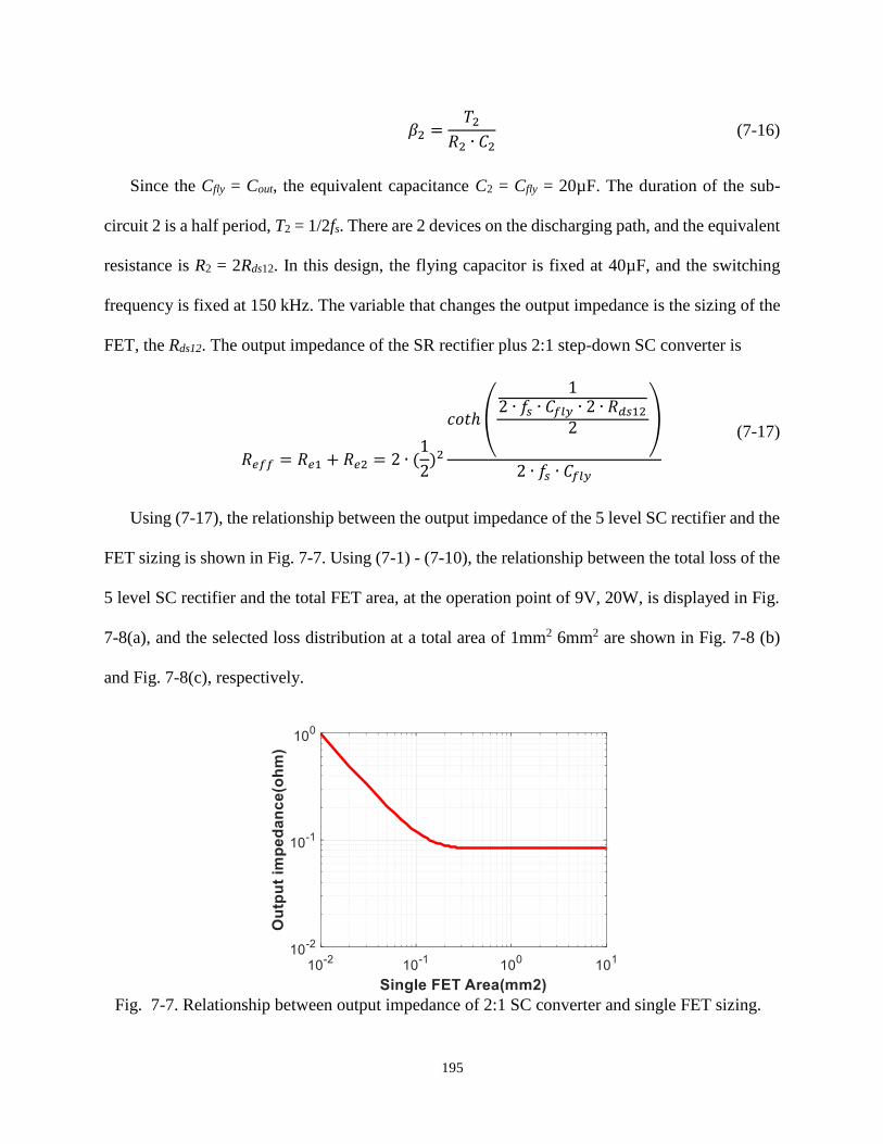
195
𝛽2 =𝑇2
𝑅2 ∙ 𝐶2 (7-16)
Since the Cfly = Cout, the equivalent capacitance C2 = Cfly = 20µF. The duration of the sub-
circuit 2 is a half period, T2 = 1/2fs. There are 2 devices on the discharging path, and the equivalent
resistance is R2 = 2Rds12. In this design, the flying capacitor is fixed at 40µF, and the switching
frequency is fixed at 150 kHz. The variable that changes the output impedance is the sizing of the
FET, the Rds12. The output impedance of the SR rectifier plus 2:1 step-down SC converter is
𝑅𝑒𝑓𝑓 = 𝑅𝑒1 + 𝑅𝑒2 = 2 ∙ (1
2)2
𝑐𝑜𝑡ℎ (
12 ∙ 𝑓𝑠 ∙ 𝐶𝑓𝑙𝑦 ∙ 2 ∙ 𝑅𝑑𝑠12
2 )
2 ∙ 𝑓𝑠 ∙ 𝐶𝑓𝑙𝑦
(7-17)
Using (7-17), the relationship between the output impedance of the 5 level SC rectifier and the
FET sizing is shown in Fig. 7-7. Using (7-1) - (7-10), the relationship between the total loss of the
5 level SC rectifier and the total FET area, at the operation point of 9V, 20W, is displayed in Fig.
7-8(a), and the selected loss distribution at a total area of 1mm2 6mm2 are shown in Fig. 7-8 (b)
and Fig. 7-8(c), respectively.
Fig. 7-7. Relationship between output impedance of 2:1 SC converter and single FET sizing.
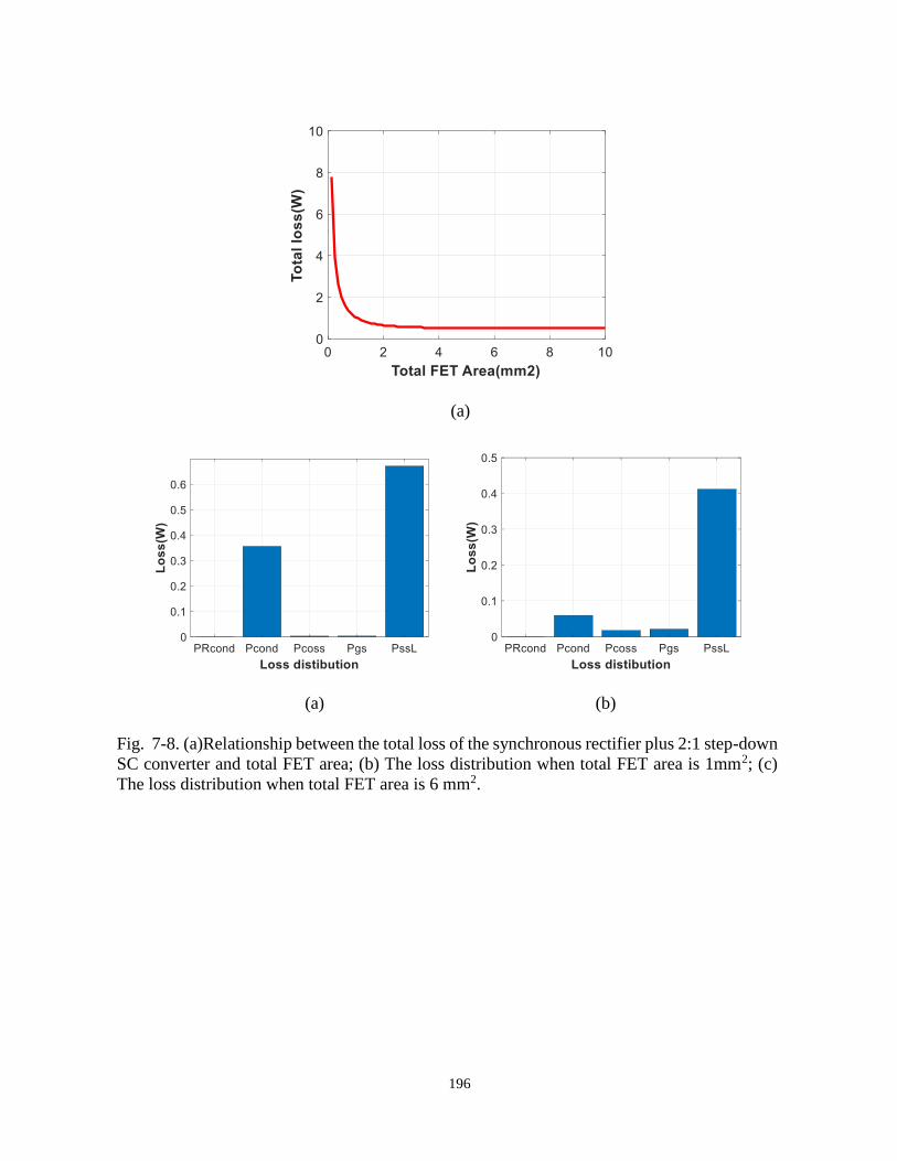
196
(a)
(a) (b)
Fig. 7-8. (a)Relationship between the total loss of the synchronous rectifier plus 2:1 step-down
SC converter and total FET area; (b) The loss distribution when total FET area is 1mm2; (c)
The loss distribution when total FET area is 6 mm2.
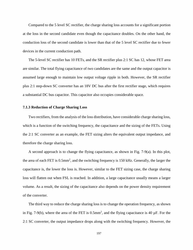
197
Compared to the 5 level SC rectifier, the charge sharing loss accounts for a significant portion
at the loss in the second candidate even though the capacitance doubles. On the other hand, the
conduction loss of the second candidate is lower than that of the 5 level SC rectifier due to fewer
devices in the current conduction path.
The 5-level SC rectifier has 10 FETs, and the SR rectifier plus 2:1 SC has 12, whose FET area
are similar. The total flying capacitance of two candidates are the same and the output capacitor is
assumed large enough to maintain low output voltage ripple in both. However, the SR rectifier
plus 2:1 step-down SC converter has an 18V DC bus after the first rectifier stage, which requires
a substantial DC bus capacitor. This capacitor also occupies considerable space.
7.1.3 Reduction of Charge Sharing Loss
Two rectifiers, from the analysis of the loss distribution, have considerable charge sharing loss,
which is a function of the switching frequency, the capacitance and the sizing of the FETs. Using
the 2:1 SC converter as an example, the FET sizing alters the equivalent output impedance, and
therefore the charge sharing loss.
A second approach is to change the flying capacitance, as shown in Fig. 7-9(a). In this plot,
the area of each FET is 0.5mm2, and the switching frequency is 150 kHz. Generally, the larger the
capacitance is, the lower the loss is. However, similar to the FET sizing case, the charge sharing
loss will flatten out when FSL is reached. In addition, a large capacitance usually means a larger
volume. As a result, the sizing of the capacitance also depends on the power density requirement
of the converter.
The third way to reduce the charge sharing loss is to change the operation frequency, as shown
in Fig. 7-9(b), where the area of the FET is 0.5mm2, and the flying capacitance is 40 µF. For the
2:1 SC converter, the output impedance drops along with the switching frequency. However, the
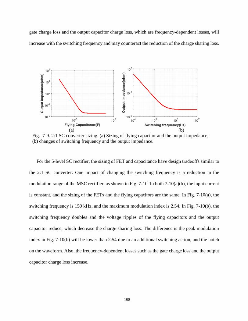
198
gate charge loss and the output capacitor charge loss, which are frequency-dependent losses, will
increase with the switching frequency and may counteract the reduction of the charge sharing loss.
For the 5-level SC rectifier, the sizing of FET and capacitance have design tradeoffs similar to
the 2:1 SC converter. One impact of changing the switching frequency is a reduction in the
modulation range of the MSC rectifier, as shown in Fig. 7-10. In both 7-10(a)(b), the input current
is constant, and the sizing of the FETs and the flying capacitors are the same. In Fig. 7-10(a), the
switching frequency is 150 kHz, and the maximum modulation index is 2.54. In Fig. 7-10(b), the
switching frequency doubles and the voltage ripples of the flying capacitors and the output
capacitor reduce, which decrease the charge sharing loss. The difference is the peak modulation
index in Fig. 7-10(b) will be lower than 2.54 due to an additional switching action, and the notch
on the waveform. Also, the frequency-dependent losses such as the gate charge loss and the output
capacitor charge loss increase.
(a) (b)
Fig. 7-9. 2:1 SC converter sizing. (a) Sizing of flying capacitor and the output impedance;
(b) changes of switching frequency and the output impedance.
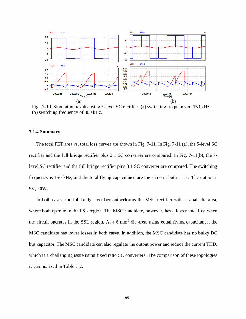
199
7.1.4 Summary
The total FET area vs. total loss curves are shown in Fig. 7-11. In Fig. 7-11 (a), the 5-level SC
rectifier and the full bridge rectifier plus 2:1 SC converter are compared. In Fig. 7-11(b), the 7-
level SC rectifier and the full bridge rectifier plus 3:1 SC converter are compared. The switching
frequency is 150 kHz, and the total flying capacitance are the same in both cases. The output is
9V, 20W.
In both cases, the full bridge rectifier outperforms the MSC rectifier with a small die area,
where both operate in the FSL region. The MSC candidate, however, has a lower total loss when
the circuit operates in the SSL region. At a 6 mm2 die area, using equal flying capacitance, the
MSC candidate has lower losses in both cases. In addition, the MSC candidate has no bulky DC
bus capacitor. The MSC candidate can also regulate the output power and reduce the current THD,
which is a challenging issue using fixed ratio SC converters. The comparison of these topologies
is summarized in Table 7-2.
(a) (b)
Fig. 7-10. Simulation results using 5-level SC rectifier. (a) switching frequency of 150 kHz;
(b) switching frequency of 300 kHz.
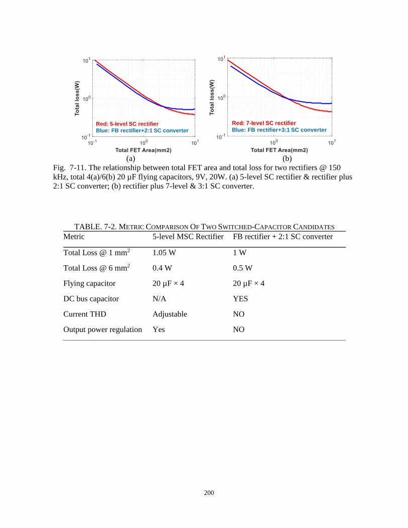
200
(a) (b)
Fig. 7-11. The relationship between total FET area and total loss for two rectifiers @ 150
kHz, total 4(a)/6(b) 20 µF flying capacitors, 9V, 20W. (a) 5-level SC rectifier & rectifier plus
2:1 SC converter; (b) rectifier plus 7-level & 3:1 SC converter.
Red: 5-level SC rectifier
Blue: FB rectifier+2:1 SC converter
Red: 7-level SC rectifier
Blue: FB rectifier+3:1 SC converter
TABLE. 7-2. METRIC COMPARISON OF TWO SWITCHED-CAPACITOR CANDIDATES
Metric 5-level MSC Rectifier FB rectifier + 2:1 SC converter
Total Loss @ 1 mm2 1.05 W 1 W
Total Loss @ 6 mm2 0.4 W 0.5 W
Flying capacitor 20 µF × 4 20 µF × 4
DC bus capacitor N/A YES
Current THD Adjustable NO
Output power regulation Yes NO

201
7.2 Regulation Design using MSC rectifier
The load for the receiver on mobile devices using wireless charging is a battery. Regulation is
needed for battery charging applications, e.g. constant voltage charging, constant current charging,
and pulsed charging. This requires the WPT receiver possess some “intelligence” to monitor the
output voltage/current, adjust the behavior of the electronic circuitries and achieve a closed-loop
control. Because MSC rectifier has output control ability, it may be possible to directly charge the
battery without an additional dc/dc charger on-board. In this section, the output voltage closed-
loop regulation using the MSC is demonstrated.
7.2.1 Output Regulation using MSC rectifier
A block diagram of output regulation with an MSC rectifier is shown in Fig. 7-12. The system
consists of a full-bridge inverter, a resonant tank, and an MSC rectifier, forming a dc-to-dc,
resonant link conversion system. For the system, the external disturbances include the variations
of the input voltage and load. To maintain the output voltage or current at desired operation points,
the WPT system can use control variables, the modulation index m of the MSC rectifier, and a
phase shift or a duty cycle of the inverter, to regulate. At the same time, the input and the output
power, or the system efficiency, maintains or changes accordingly.
The regulation goal is to maintain a desired output voltage/current at a high efficiency when
the input or the load changes. For a given power supply, there is a limitation where the control
variables can regulate the output at given input, which is defined as the regulation boundary. The
regulation boundary of the WPT system is shown in Fig. 7-13, and the circuit parameters are given
in the table below.
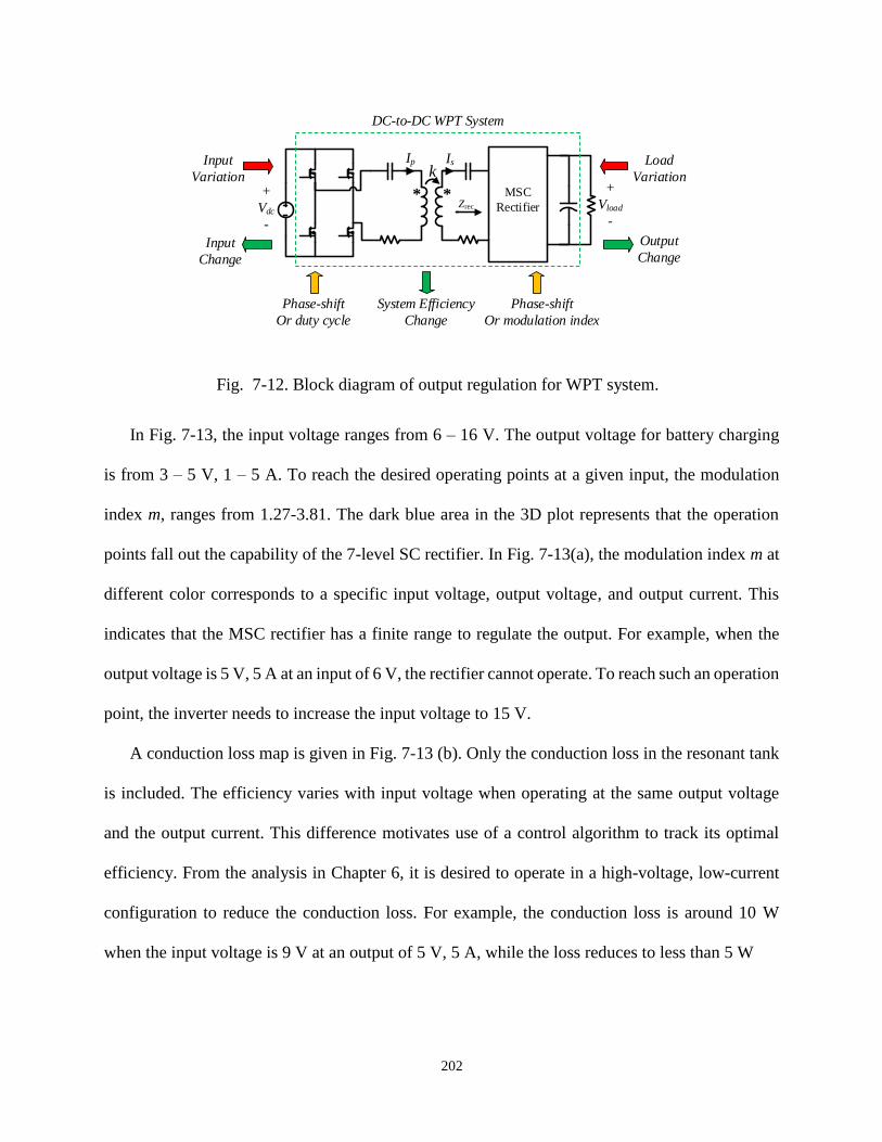
202
In Fig. 7-13, the input voltage ranges from 6 – 16 V. The output voltage for battery charging
is from 3 – 5 V, 1 – 5 A. To reach the desired operating points at a given input, the modulation
index m, ranges from 1.27-3.81. The dark blue area in the 3D plot represents that the operation
points fall out the capability of the 7-level SC rectifier. In Fig. 7-13(a), the modulation index m at
different color corresponds to a specific input voltage, output voltage, and output current. This
indicates that the MSC rectifier has a finite range to regulate the output. For example, when the
output voltage is 5 V, 5 A at an input of 6 V, the rectifier cannot operate. To reach such an operation
point, the inverter needs to increase the input voltage to 15 V.
A conduction loss map is given in Fig. 7-13 (b). Only the conduction loss in the resonant tank
is included. The efficiency varies with input voltage when operating at the same output voltage
and the output current. This difference motivates use of a control algorithm to track its optimal
efficiency. From the analysis in Chapter 6, it is desired to operate in a high-voltage, low-current
configuration to reduce the conduction loss. For example, the conduction loss is around 10 W
when the input voltage is 9 V at an output of 5 V, 5 A, while the loss reduces to less than 5 W
* *
k+
Vload
-
Ip Is
Zrec
MSC
Rectifier
+
Vdc
-
Input
Variation
Load
Variation
Phase-shift
Or duty cycle
Phase-shift
Or modulation index
DC-to-DC WPT System
Output
ChangeInput
Change
System Efficiency
Change
Fig. 7-12. Block diagram of output regulation for WPT system.
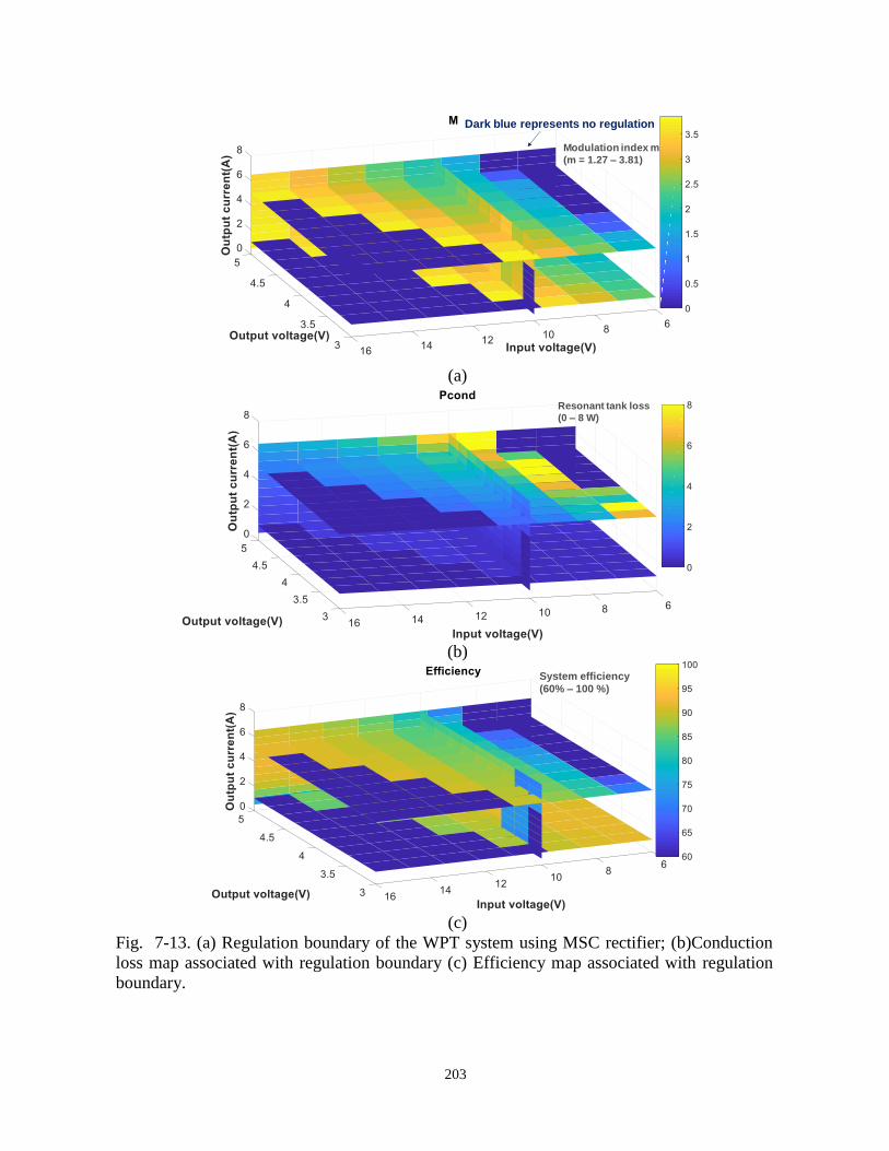
203
(a)
(b)
(c)
Fig. 7-13. (a) Regulation boundary of the WPT system using MSC rectifier; (b)Conduction
loss map associated with regulation boundary (c) Efficiency map associated with regulation
boundary.
Modulation index m
(m = 1.27 – 3.81)
Dark blue represents no regulation
Resonant tank loss
(0 – 8 W)
System efficiency
(60% – 100 %)
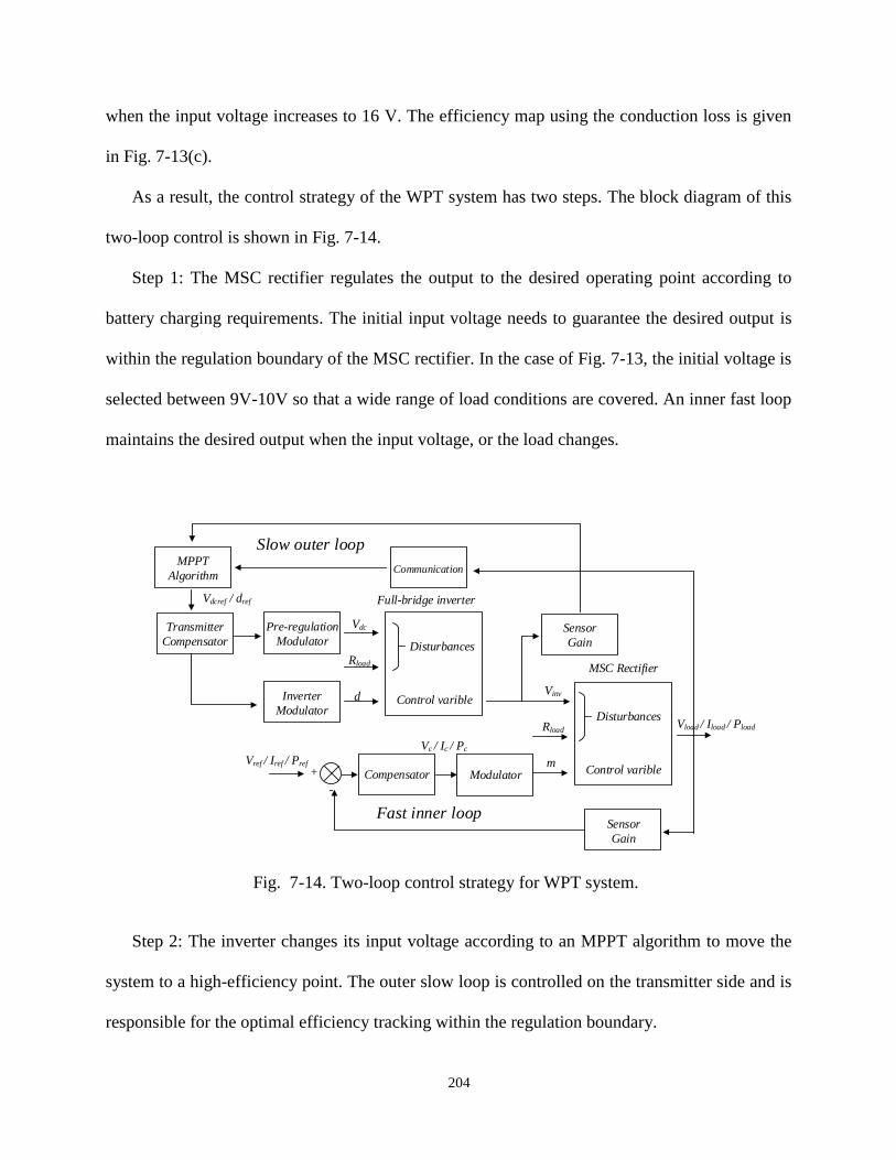
204
when the input voltage increases to 16 V. The efficiency map using the conduction loss is given
in Fig. 7-13(c).
As a result, the control strategy of the WPT system has two steps. The block diagram of this
two-loop control is shown in Fig. 7-14.
Step 1: The MSC rectifier regulates the output to the desired operating point according to
battery charging requirements. The initial input voltage needs to guarantee the desired output is
within the regulation boundary of the MSC rectifier. In the case of Fig. 7-13, the initial voltage is
selected between 9V-10V so that a wide range of load conditions are covered. An inner fast loop
maintains the desired output when the input voltage, or the load changes.
Step 2: The inverter changes its input voltage according to an MPPT algorithm to move the
system to a high-efficiency point. The outer slow loop is controlled on the transmitter side and is
responsible for the optimal efficiency tracking within the regulation boundary.
MSC Rectifier
Vinv
Rload
m
Disturbances
Control varible+
-
Vref / Iref / Pref
Vload / Iload / Pload
Sensor
Gain
Compensator Modulator
Vc / Ic / Pc
Fast inner loop
Vdc
Rload
d
Full-bridge inverter
Disturbances
Control varible
Communication
Transmitter
Compensator
Pre-regulation
Modulator
Inverter
Modulator
MPPT
Algorithm
Vdcref / dref
Sensor
Gain
Slow outer loop
Fig. 7-14. Two-loop control strategy for WPT system.
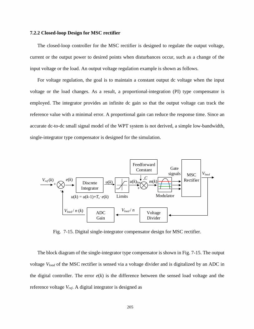
205
7.2.2 Closed-loop Design for MSC rectifier
The closed-loop controller for the MSC rectifier is designed to regulate the output voltage,
current or the output power to desired points when disturbances occur, such as a change of the
input voltage or the load. An output voltage regulation example is shown as follows.
For voltage regulation, the goal is to maintain a constant output dc voltage when the input
voltage or the load changes. As a result, a proportional-integration (PI) type compensator is
employed. The integrator provides an infinite dc gain so that the output voltage can track the
reference value with a minimal error. A proportional gain can reduce the response time. Since an
accurate dc-to-dc small signal model of the WPT system is not derived, a simple low-bandwidth,
single-integrator type compensator is designed for the simulation.
The block diagram of the single-integrator type compensator is shown in Fig. 7-15. The output
voltage Vload of the MSC rectifier is sensed via a voltage divider and is digitalized by an ADC in
the digital controller. The error e(k) is the difference between the sensed load voltage and the
reference voltage Vref. A digital integrator is designed as
MSC
Rectifier
Vload
+
-
Vref (k)
Voltage
Divider
ADC
Gain
Vload / n Vload / n (k)
Discrete
Integrator
e(k)
u(k) = u(k-1)+Ts e(k)
+
-
Feedforward
Constant
u(k)C
Limits
m(k)
Modulator
u(k)lim
Gate
signals
Fig. 7-15. Digital single-integrator compensator design for MSC rectifier.
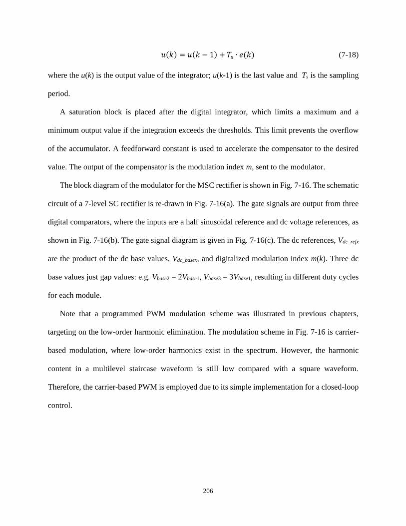
206
𝑢(𝑘) = 𝑢(𝑘 − 1) + 𝑇𝑠 ∙ 𝑒(𝑘) (7-18)
where the u(k) is the output value of the integrator; u(k-1) is the last value and Ts is the sampling
period.
A saturation block is placed after the digital integrator, which limits a maximum and a
minimum output value if the integration exceeds the thresholds. This limit prevents the overflow
of the accumulator. A feedforward constant is used to accelerate the compensator to the desired
value. The output of the compensator is the modulation index m, sent to the modulator.
The block diagram of the modulator for the MSC rectifier is shown in Fig. 7-16. The schematic
circuit of a 7-level SC rectifier is re-drawn in Fig. 7-16(a). The gate signals are output from three
digital comparators, where the inputs are a half sinusoidal reference and dc voltage references, as
shown in Fig. 7-16(b). The gate signal diagram is given in Fig. 7-16(c). The dc references, Vdc_refx
are the product of the dc base values, Vdc_basex, and digitalized modulation index m(k). Three dc
base values just gap values: e.g. Vbase2 = 2Vbase1, Vbase3 = 3Vbase1, resulting in different duty cycles
for each module.
Note that a programmed PWM modulation scheme was illustrated in previous chapters,
targeting on the low-order harmonic elimination. The modulation scheme in Fig. 7-16 is carrier-
based modulation, where low-order harmonics exist in the spectrum. However, the harmonic
content in a multilevel staircase waveform is still low compared with a square waveform.
Therefore, the carrier-based PWM is employed due to its simple implementation for a closed-loop
control.
207
Ls
Cs
Iin
Rs
-
Vrec
+
Vin
Rload
C1A
C2A
C3A
C1B
C2B
C3B
Cout
+
Vload
-
SC1Aa b
Phase
Leg A
Phase
Leg B
S1AH
SC2A
SC1B
SC2B
S1AL
S2AH
S2AL
S3AH
S3AL
S1BH
S1BL
S2BH
S2BL
S3BH
S3BL
×
Vdc_ref1
sine_ref
dc_base
Vdc_ref2
Vdc_ref3
Gate signalsComparator
From
compensator
m(k)
(a) (b)
Half Sine
Reference
Vs in e_ref
Vdc_ref1=Vdc_base1 m
SC1A
T/2t1 t2 t3 t4 t5 t6
S1AH(S1AL)
SC2A
S2AH(S2AL)
S3AH(S3AL)
Vdc_ref2=Vdc_base2 m
Vdc_ref3=Vdc_base3 m
(c)
Fig. 7-16. Modulator design for MSC rectifier. (a) Schematic circuit of MSC rectifier; (b)
Block diagram of carrier-based modulator; (c) Gate signal diagram,
208
A load change simulation is given in Fig. 7-17. The input voltage on the transmitter side keeps
constant, and the load changes from 20W to 0.5W at 0.1s. In Fig. 7-17(a), the rectifier output
voltage tracks the reference 5V before and after 0.1s. Since only a low-bandwidth compensator is
used, the response time takes about 1s to re-settle to the reference after the load change. The
voltage and current waveforms of the inverter and the MSC rectifier are shown in Fig. 7-17(b).
From the results in Fig. 7-17, the closed-loop controller can regulate the output voltage over a wide
load change.
An input change simulation is given in Fig. 7-18. The load is a fixed resistance, and the input
voltage changes from 10V to 13V at 0.1s on the transmitter side. In Fig. 7-18(a), the rectifier output
voltage tracks the reference 5V before and after 0.1s. The voltage and current waveforms of the
inverter and the MSC rectifier are shown in Fig. 7-18(b). From the results in Fig. 7-18, the closed-
loop controller can regulate the output voltage for an input voltage change.
For battery charging applications, the output voltage needs to change the reference value
according to the state of charge of the battery. A reference tracking simulation is shown in Fig. 7-
19, where the input voltage and the load keep constant, and the output reference gradually increases
from 5V to about 6V. The output voltage tracks the new reference and stabilized after 0.3s.
The designed closed-loop controller successfully demonstrates the output regulation ability for
the input change, the load change and the reference change with the MSC rectifier. The dynamic
performance is acceptable for battery charging applications, and the response time could be further
improved with accurate small signal modeling of the WPT system.
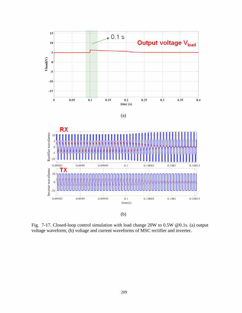
209
(a)
(b)
Fig. 7-17. Closed-loop control simulation with load change 20W to 0.5W @0.1s. (a) output
voltage waveform; (b) voltage and current waveforms of MSC rectifier and inverter.
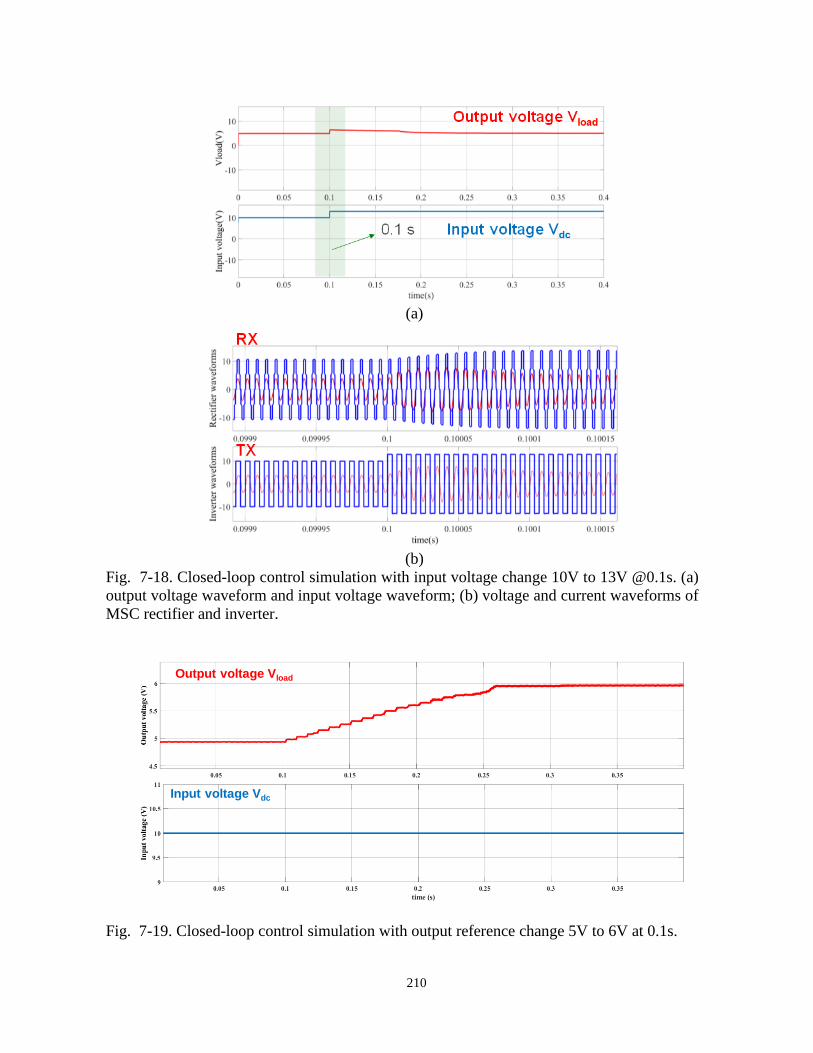
210
(a)
(b)
Fig. 7-18. Closed-loop control simulation with input voltage change 10V to 13V @0.1s. (a)
output voltage waveform and input voltage waveform; (b) voltage and current waveforms of
MSC rectifier and inverter.
Fig. 7-19. Closed-loop control simulation with output reference change 5V to 6V at 0.1s.
Input voltage Vdc
Output voltage Vload
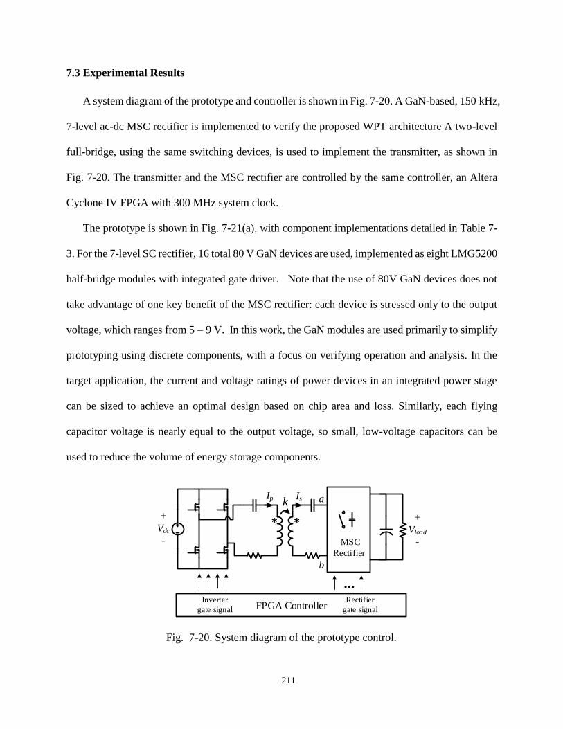
211
7.3 Experimental Results
A system diagram of the prototype and controller is shown in Fig. 7-20. A GaN-based, 150 kHz,
7-level ac-dc MSC rectifier is implemented to verify the proposed WPT architecture A two-level
full-bridge, using the same switching devices, is used to implement the transmitter, as shown in
Fig. 7-20. The transmitter and the MSC rectifier are controlled by the same controller, an Altera
Cyclone IV FPGA with 300 MHz system clock.
The prototype is shown in Fig. 7-21(a), with component implementations detailed in Table 7-
3. For the 7-level SC rectifier, 16 total 80 V GaN devices are used, implemented as eight LMG5200
half-bridge modules with integrated gate driver. Note that the use of 80V GaN devices does not
take advantage of one key benefit of the MSC rectifier: each device is stressed only to the output
voltage, which ranges from 5 – 9 V. In this work, the GaN modules are used primarily to simplify
prototyping using discrete components, with a focus on verifying operation and analysis. In the
target application, the current and voltage ratings of power devices in an integrated power stage
can be sized to achieve an optimal design based on chip area and loss. Similarly, each flying
capacitor voltage is nearly equal to the output voltage, so small, low-voltage capacitors can be
used to reduce the volume of energy storage components.
* *
k
+
Vload
-
Ip Is
b
a
MSC
Rectifier
+
Vdc
-
FPGA ControllerInverter
gate signal
Rectifier
gate signal
...
Fig. 7-20. System diagram of the prototype control.
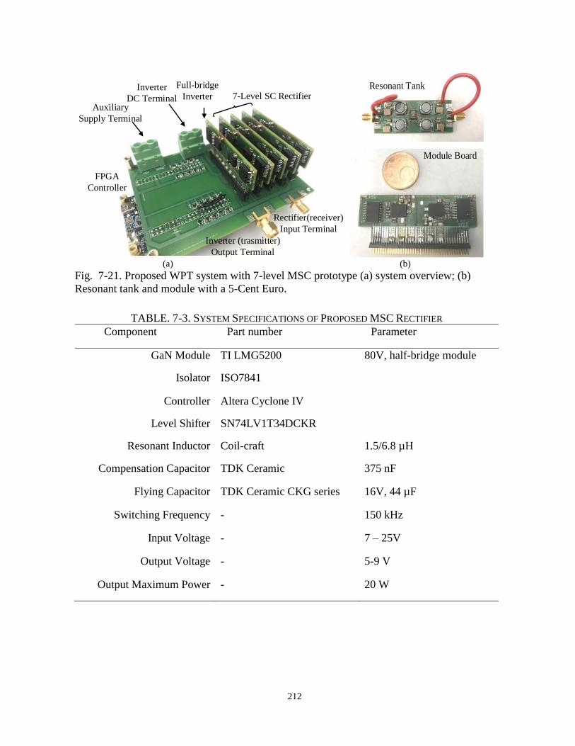
212
Auxiliary
Supply Terminal
Inverter
DC Terminal 7-Level SC Rectifier
Full-bridge
Inverter
Rectifier(receiver)
Input Terminal
Inverter (trasmitter)
Output Terminal
FPGA
Controller
Resonant Tank
Module Board
(a) (b)
Fig. 7-21. Proposed WPT system with 7-level MSC prototype (a) system overview; (b)
Resonant tank and module with a 5-Cent Euro.
TABLE. 7-3. SYSTEM SPECIFICATIONS OF PROPOSED MSC RECTIFIER
Component Part number Parameter
GaN Module TI LMG5200 80V, half-bridge module
Isolator ISO7841
Controller Altera Cyclone IV
Level Shifter SN74LV1T34DCKR
Resonant Inductor Coil-craft 1.5/6.8 µH
Compensation Capacitor TDK Ceramic 375 nF
Flying Capacitor TDK Ceramic CKG series 16V, 44 µF
Switching Frequency - 150 kHz
Input Voltage - 7 – 25V
Output Voltage - 5-9 V
Output Maximum Power - 20 W
213
A passive L-C network, shown in Fig. 7-21(b), is used to emulate a pair of fixed-position WPT
coils. Surface mount inductors and capacitors implement a series-series resonant network. The
network is designed to emulate a 0.7 coupling coefficient and is tuned to 150 kHz resonant
frequency. The series parasitic resistances, Rp and Rs of the resonant tanks, are measured as 200
mΩ using Agilent 4294A impedance analyzer. This resistance results in a quality factor of Q = 60,
which is comparable to commercial low-profile WPT coils. Combined with the transmitter, this
tank facilitates evaluation of the performance of the 7-level SC rectifier using dc-dc efficiency
measurements of the entire WPT system.
7.3.1 Efficiency test
Using the platform shown in Fig. 7-21, the efficiency and a comparison with the conventional
diode rectifier are tested in the section. Fig. 7-22 gives experimental waveforms for the 7-level
MSC rectifier providing full 20 W output power to a 2 Ω electronic load, resulting in an output
voltage of 6.3 V. In this case, the MSC employs SHE modulation with m = 2.5, where the 3rd and
5th harmonics are eliminated in Vrec. Queue charge control is employed, since voltage and current
are in phase, and the gate signals for the high-side and charge balance switches in one phase leg
are given in Fig. 7-23. Fig. 7-24 shows the voltages of the flying capacitors C1A, C2A and C3A in
Phase Leg A using the queue charge control. The voltage ripple is very small (several mV) in this
case, as predicted in the simulation results, and the charge sharing loss is illustrated in the loss
analysis.
With the same transmitter and resonant tank, the MSC rectifier is replaced with a traditional
two-level diode bridge rectifier. The rectifier input voltage and current are shown in Fig. 7-25(a)
and the spectrum of Vrec is given in Fig. 7-25 (b). Substantial 3rd and 5th harmonics are present with
the diode rectifier, requiring additional low-order harmonic filters for attenuation in practice.
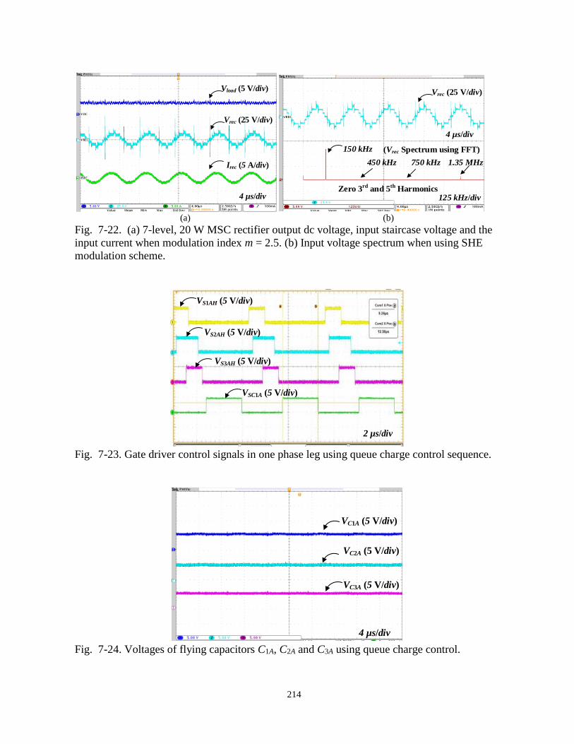
214
Vload (5 V/div)
Vrec (25 V/div)
Irec (5 A/div)
4 µs/div
Vrec (25 V/div)
4 µs/div
125 kHz/divZero 3rd and 5th Harmonics
150 kHz
450 kHz 750 kHz 1.35 MHz
(Vrec Spectrum using FFT)
(a) (b)
Fig. 7-22. (a) 7-level, 20 W MSC rectifier output dc voltage, input staircase voltage and the
input current when modulation index m = 2.5. (b) Input voltage spectrum when using SHE
modulation scheme.
VS1AH (5 V/div)
2 µs/div
VS2AH (5 V/div)
VS3AH (5 V/div)
VSC1A (5 V/div)
Fig. 7-23. Gate driver control signals in one phase leg using queue charge control sequence.
VC2A (5 V/div)
VC3A (5 V/div)
4 µs/div
VC1A (5 V/div)
Fig. 7-24. Voltages of flying capacitors C1A, C2A and C3A using queue charge control.
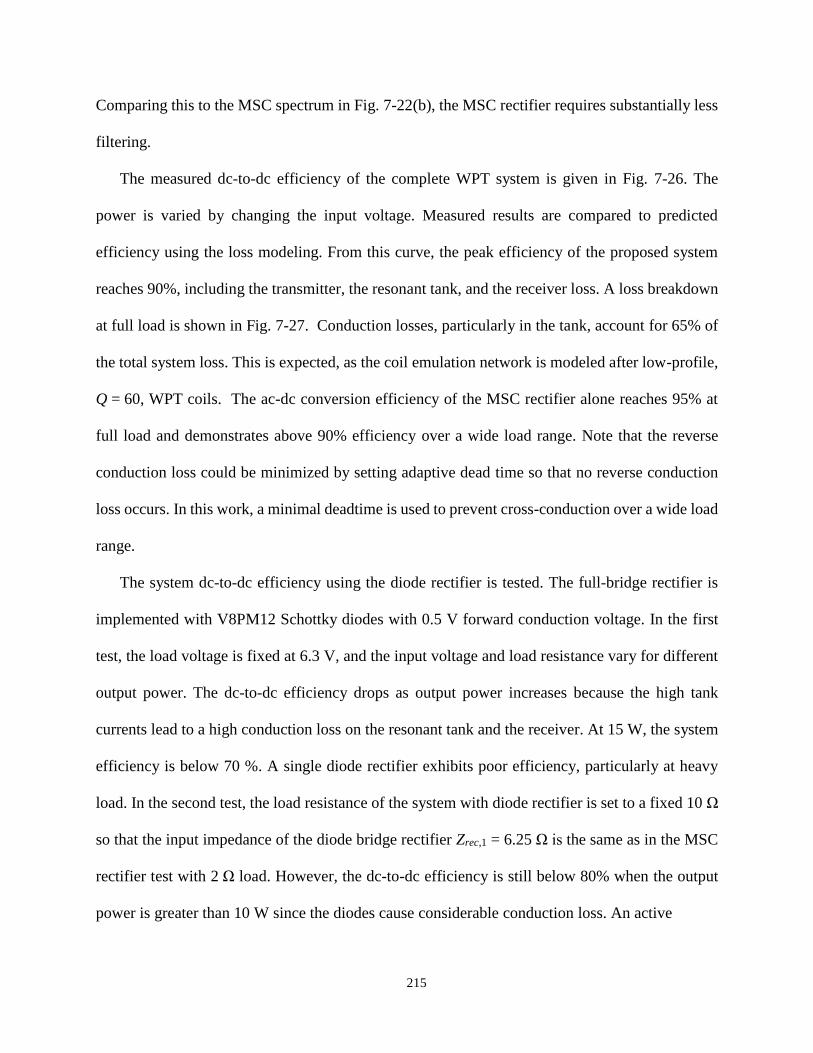
215
Comparing this to the MSC spectrum in Fig. 7-22(b), the MSC rectifier requires substantially less
filtering.
The measured dc-to-dc efficiency of the complete WPT system is given in Fig. 7-26. The
power is varied by changing the input voltage. Measured results are compared to predicted
efficiency using the loss modeling. From this curve, the peak efficiency of the proposed system
reaches 90%, including the transmitter, the resonant tank, and the receiver loss. A loss breakdown
at full load is shown in Fig. 7-27. Conduction losses, particularly in the tank, account for 65% of
the total system loss. This is expected, as the coil emulation network is modeled after low-profile,
Q = 60, WPT coils. The ac-dc conversion efficiency of the MSC rectifier alone reaches 95% at
full load and demonstrates above 90% efficiency over a wide load range. Note that the reverse
conduction loss could be minimized by setting adaptive dead time so that no reverse conduction
loss occurs. In this work, a minimal deadtime is used to prevent cross-conduction over a wide load
range.
The system dc-to-dc efficiency using the diode rectifier is tested. The full-bridge rectifier is
implemented with V8PM12 Schottky diodes with 0.5 V forward conduction voltage. In the first
test, the load voltage is fixed at 6.3 V, and the input voltage and load resistance vary for different
output power. The dc-to-dc efficiency drops as output power increases because the high tank
currents lead to a high conduction loss on the resonant tank and the receiver. At 15 W, the system
efficiency is below 70 %. A single diode rectifier exhibits poor efficiency, particularly at heavy
load. In the second test, the load resistance of the system with diode rectifier is set to a fixed 10 Ω
so that the input impedance of the diode bridge rectifier Zrec,1 = 6.25 Ω is the same as in the MSC
rectifier test with 2 Ω load. However, the dc-to-dc efficiency is still below 80% when the output
power is greater than 10 W since the diodes cause considerable conduction loss. An active
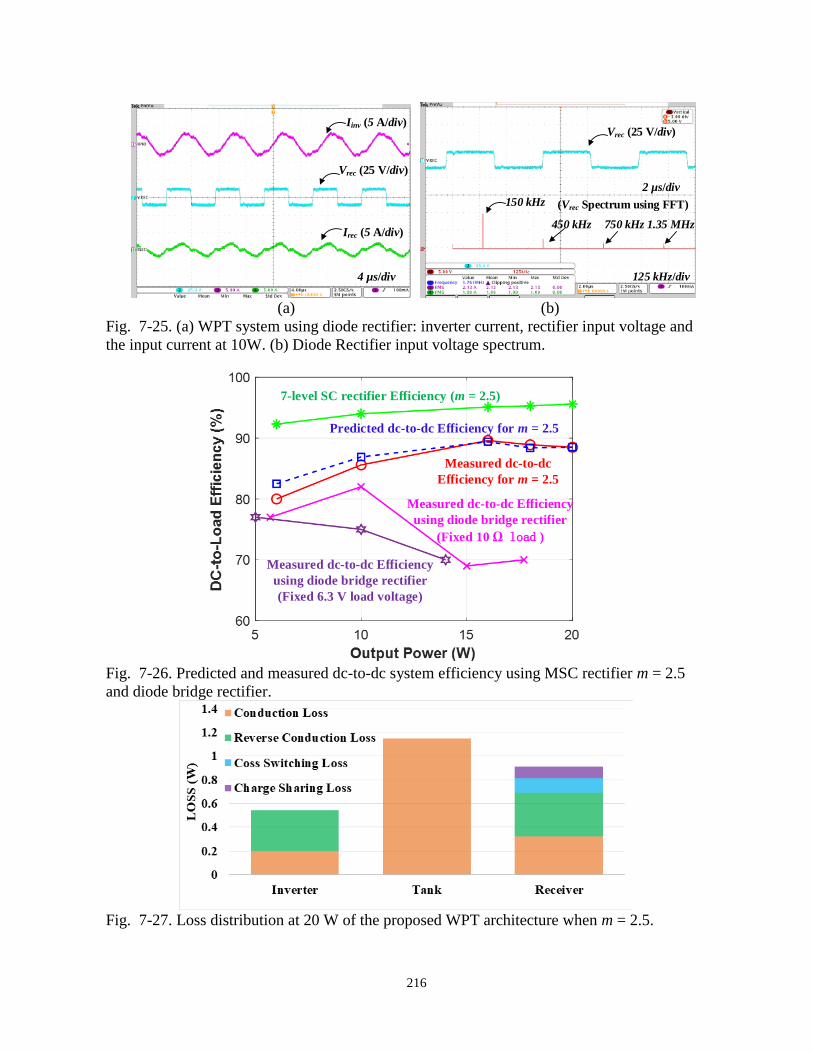
216
(a) (b)
Fig. 7-25. (a) WPT system using diode rectifier: inverter current, rectifier input voltage and
the input current at 10W. (b) Diode Rectifier input voltage spectrum.
Fig. 7-26. Predicted and measured dc-to-dc system efficiency using MSC rectifier m = 2.5
and diode bridge rectifier.
Fig. 7-27. Loss distribution at 20 W of the proposed WPT architecture when m = 2.5.
Vrec (25 V/div)
Irec (5 A/div)
4 µs/div
Iinv (5 A/div)Vrec (25 V/div)
2 µs/div
125 kHz/div
150 kHz
450 kHz 750 kHz 1.35 MHz
(Vrec Spectrum using FFT)
Predicted dc-to-dc Efficiency for m = 2.5
Measured dc-to-dc
Efficiency for m = 2.5
Measured dc-to-dc Efficiency
using diode bridge rectifier
(Fixed 10 load )
7-level SC rectifier Efficiency (m = 2.5)
Measured dc-to-dc Efficiency
using diode bridge rectifier
(Fixed 6.3 V load voltage)
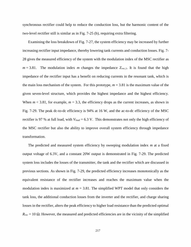
217
synchronous rectifier could help to reduce the conduction loss, but the harmonic content of the
two-level rectifier still is similar as in Fig. 7-25 (b), requiring extra filtering.
Examining the loss breakdown of Fig. 7-27, the system efficiency may be increased by further
increasing rectifier input impedance, thereby lowering tank currents and conduction losses. Fig. 7-
28 gives the measured efficiency of the system with the modulation index of the MSC rectifier as
m = 3.81. The modulation index m changes the impedance Zrec,1. It is found that the high
impedance of the rectifier input has a benefit on reducing currents in the resonant tank, which is
the main loss mechanism of the system. For this prototype, m = 3.81 is the maximum value of the
given seven-level structure, which provides the highest impedance and the highest efficiency.
When m < 3.81, for example, m = 3.3, the efficiency drops as the current increases, as shown in
Fig. 7-29. The peak dc-to-dc efficiency is 94% at 16 W, and the ac-to-dc efficiency of the MSC
rectifier is 97 % at full load, with Vload = 6.3 V. This demonstrates not only the high efficiency of
the MSC rectifier but also the ability to improve overall system efficiency through impedance
transformation.
The predicted and measured system efficiency by sweeping modulation index m at a fixed
output voltage of 6.3V, and a constant 20W output is demonstrated in Fig. 7-29. The predicted
system loss includes the losses of the transmitter, the tank and the rectifier which are discussed in
previous sections. As shown in Fig. 7-29, the predicted efficiency increases monotonically as the
equivalent resistance of the rectifier increases and reaches the maximum value when the
modulation index is maximized at m = 3.81. The simplified WPT model that only considers the
tank loss, the additional conduction losses from the inverter and the rectifier, and charge sharing
losses in the rectifier, alters the peak efficiency to higher load resistance than the predicted optimal
Rrec = 10 Ω. However, the measured and predicted efficiencies are in the vicinity of the simplified
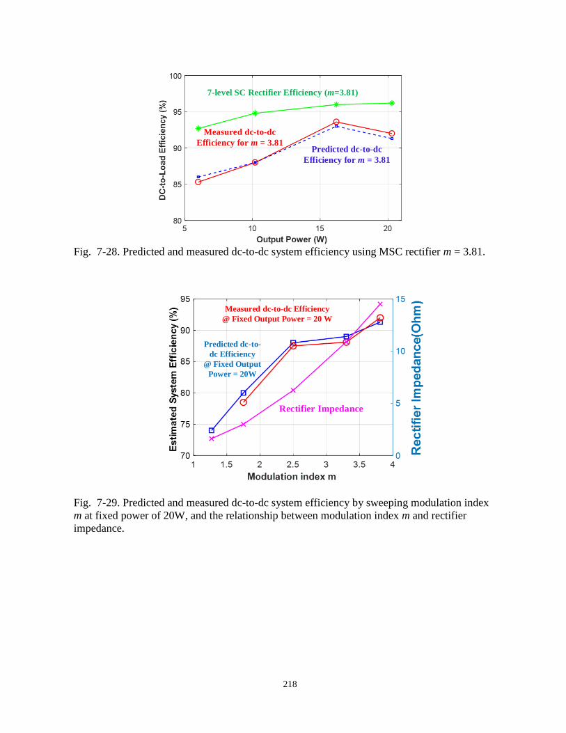
218
7-level SC Rectifier Efficiency (m=3.81)
Measured dc-to-dc
Efficiency for m = 3.81Predicted dc-to-dc
Efficiency for m = 3.81
Fig. 7-28. Predicted and measured dc-to-dc system efficiency using MSC rectifier m = 3.81.
Predicted dc-to-
dc Efficiency
@ Fixed Output
Power = 20W
Rectifier Impedance
Measured dc-to-dc Efficiency
@ Fixed Output Power = 20 W
Fig. 7-29. Predicted and measured dc-to-dc system efficiency by sweeping modulation index
m at fixed power of 20W, and the relationship between modulation index m and rectifier
impedance.
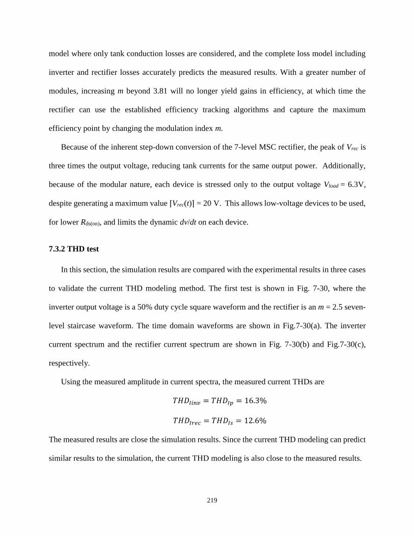
219
model where only tank conduction losses are considered, and the complete loss model including
inverter and rectifier losses accurately predicts the measured results. With a greater number of
modules, increasing m beyond 3.81 will no longer yield gains in efficiency, at which time the
rectifier can use the established efficiency tracking algorithms and capture the maximum
efficiency point by changing the modulation index m.
Because of the inherent step-down conversion of the 7-level MSC rectifier, the peak of Vrec is
three times the output voltage, reducing tank currents for the same output power. Additionally,
because of the modular nature, each device is stressed only to the output voltage Vload = 6.3V,
despite generating a maximum value ⌈Vrec(t)⌉ = 20 V. This allows low-voltage devices to be used,
for lower Rds(on), and limits the dynamic dv/dt on each device.
7.3.2 THD test
In this section, the simulation results are compared with the experimental results in three cases
to validate the current THD modeling method. The first test is shown in Fig. 7-30, where the
inverter output voltage is a 50% duty cycle square waveform and the rectifier is an m = 2.5 seven-
level staircase waveform. The time domain waveforms are shown in Fig.7-30(a). The inverter
current spectrum and the rectifier current spectrum are shown in Fig. 7-30(b) and Fig.7-30(c),
respectively.
Using the measured amplitude in current spectra, the measured current THDs are
𝑇𝐻𝐷𝐼𝑖𝑛𝑣 = 𝑇𝐻𝐷𝐼𝑝 = 16.3%
𝑇𝐻𝐷𝐼𝑟𝑒𝑐 = 𝑇𝐻𝐷𝐼𝑠 = 12.6%
The measured results are close the simulation results. Since the current THD modeling can predict
similar results to the simulation, the current THD modeling is also close to the measured results.
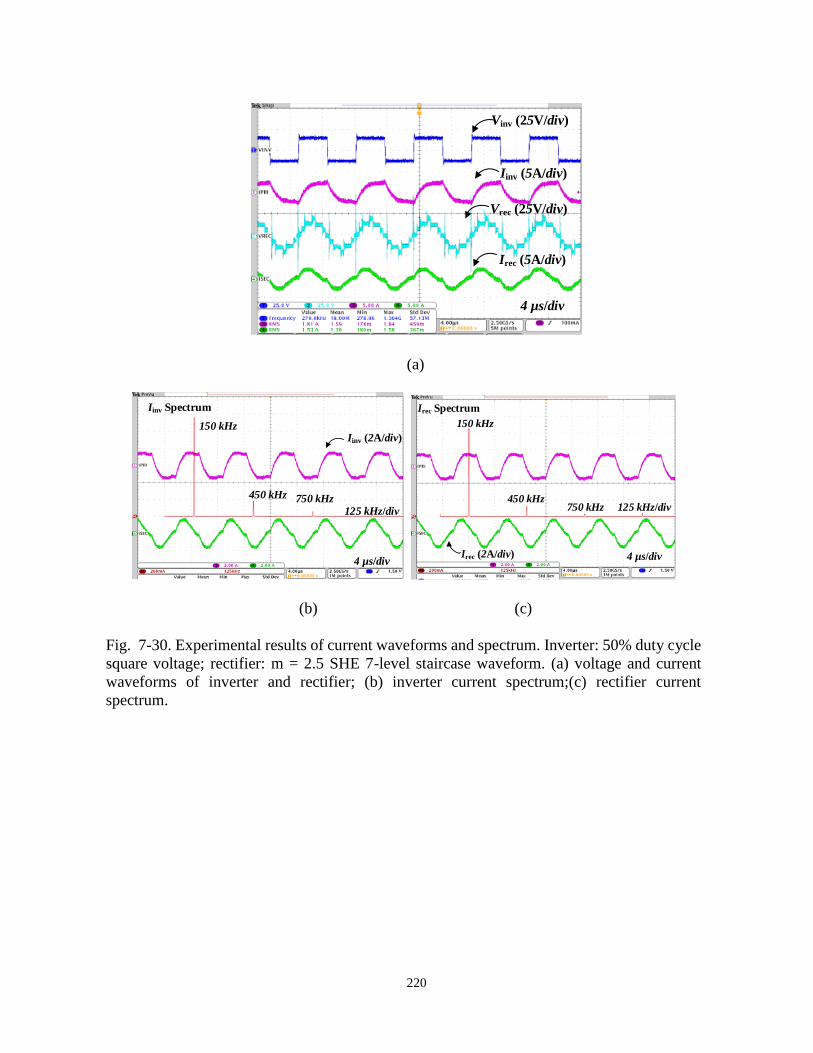
220
Vinv (25V/div)
Iinv (5A/div)
Vrec (25V/div)
Irec (5A/div)
4 µs/div
(a)
Iinv (2A/div)150 kHz
450 kHz 750 kHz
4 µs/div
125 kHz/div
Iinv Spectrum
Irec (2A/div)
150 kHz
450 kHz750 kHz
4 µs/div
125 kHz/div
Irec Spectrum
(b) (c)
Fig. 7-30. Experimental results of current waveforms and spectrum. Inverter: 50% duty cycle
square voltage; rectifier: m = 2.5 SHE 7-level staircase waveform. (a) voltage and current
waveforms of inverter and rectifier; (b) inverter current spectrum;(c) rectifier current
spectrum.
221
The second test is shown in Fig. 7-31, where the inverter output voltage is a 50% duty cycle
square waveform and the rectifier is an m = 3.81 square waveform. The time domain waveforms
are shown in Fig.7-31(a). The inverter current spectrum and the rectifier current spectrum are
shown in Fig. 7-31(b) and Fig.7-31(c), respectively. As predicted using THD modeling, a square
voltage of the rectifier input is beneficial for the current THD minimization, if the inverter output
is a square waveform. Using the measured amplitude in current spectra, the measured current
THDs
𝑇𝐻𝐷𝐼𝑖𝑛𝑣 = 𝑇𝐻𝐷𝐼𝑝 = 7.3%
𝑇𝐻𝐷𝐼𝑟𝑒𝑐 = 𝑇𝐻𝐷𝐼𝑠 = 6.4%
However, considerable the 3rd and the 5th harmonics exist in the square waveforms, and some
residual low-order harmonic contents are in the current spectrum, as shown in Fig. 7-31(b) and
Fig. 7-31(c). To further reduce the harmonic content in the current spectra, the THD minimization
approach that utilizes dual-SHE configuration is employed, as demonstrated in Fig. 7-32.
In Fig. 7-32, the inverter employs a unipolar m = 1 SHE modulation scheme, while the rectifier
employs a multilevel m =2.5 SHE modulation scheme. With dual-SHE configuration, no 3rd and
5th harmonics are present in the system. The time domain waveforms are shown in Fig.7-32(a).
The inverter current spectrum and the rectifier current spectrum are shown in Fig. 7-32(b) and
Fig.7-32(c), respectively. The currents on both sides are sinusoidal waveforms with less harmonic
content, as shown in Fig. 7-32(b) and Fig. 7-32(c). Using the measured amplitude in current spectra,
the measured current THDs
𝑇𝐻𝐷𝐼𝑖𝑛𝑣 = 𝑇𝐻𝐷𝐼𝑝 = 1%
𝑇𝐻𝐷𝐼𝑟𝑒𝑐 = 𝑇𝐻𝐷𝐼𝑠 = 1%
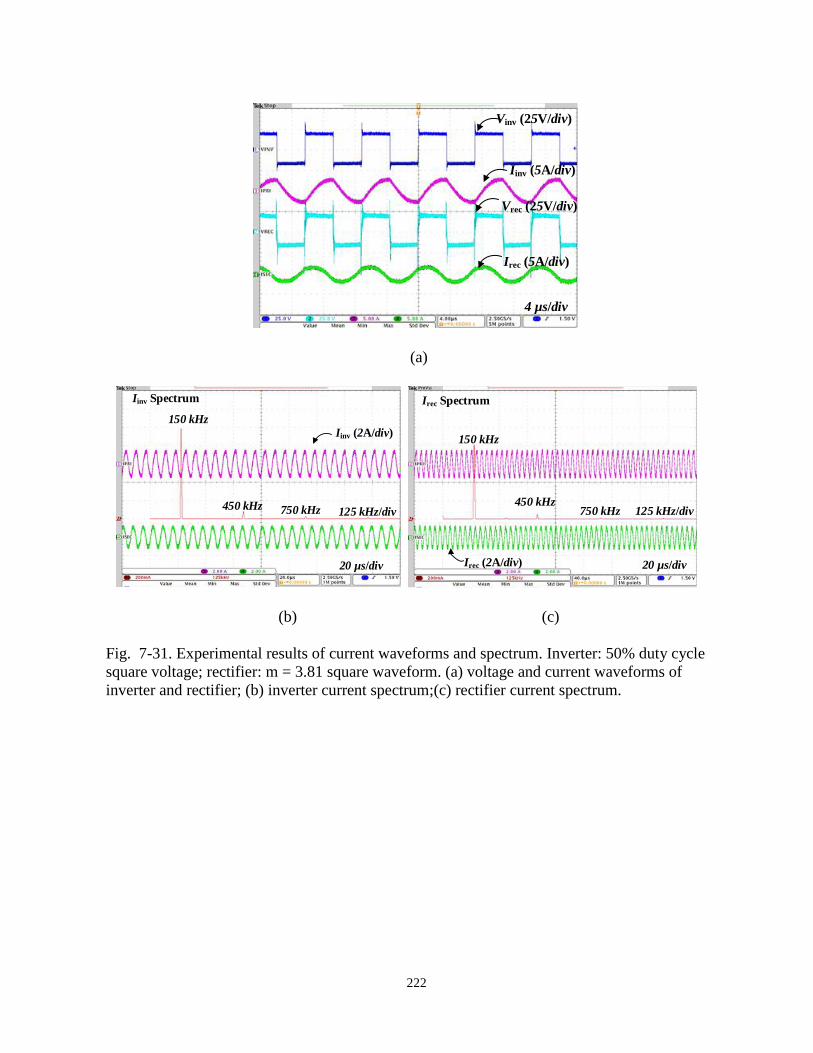
222
Vinv (25V/div)
Iinv (5A/div)
Vrec (25V/div)
Irec (5A/div)
4 µs/div
(a)
Iinv (2A/div)
150 kHz
450 kHz 750 kHz
20 µs/div
125 kHz/div
Iinv Spectrum
Irec (2A/div)
150 kHz
450 kHz750 kHz
20 µs/div
125 kHz/div
Irec Spectrum
(b) (c)
Fig. 7-31. Experimental results of current waveforms and spectrum. Inverter: 50% duty cycle
square voltage; rectifier: m = 3.81 square waveform. (a) voltage and current waveforms of
inverter and rectifier; (b) inverter current spectrum;(c) rectifier current spectrum.
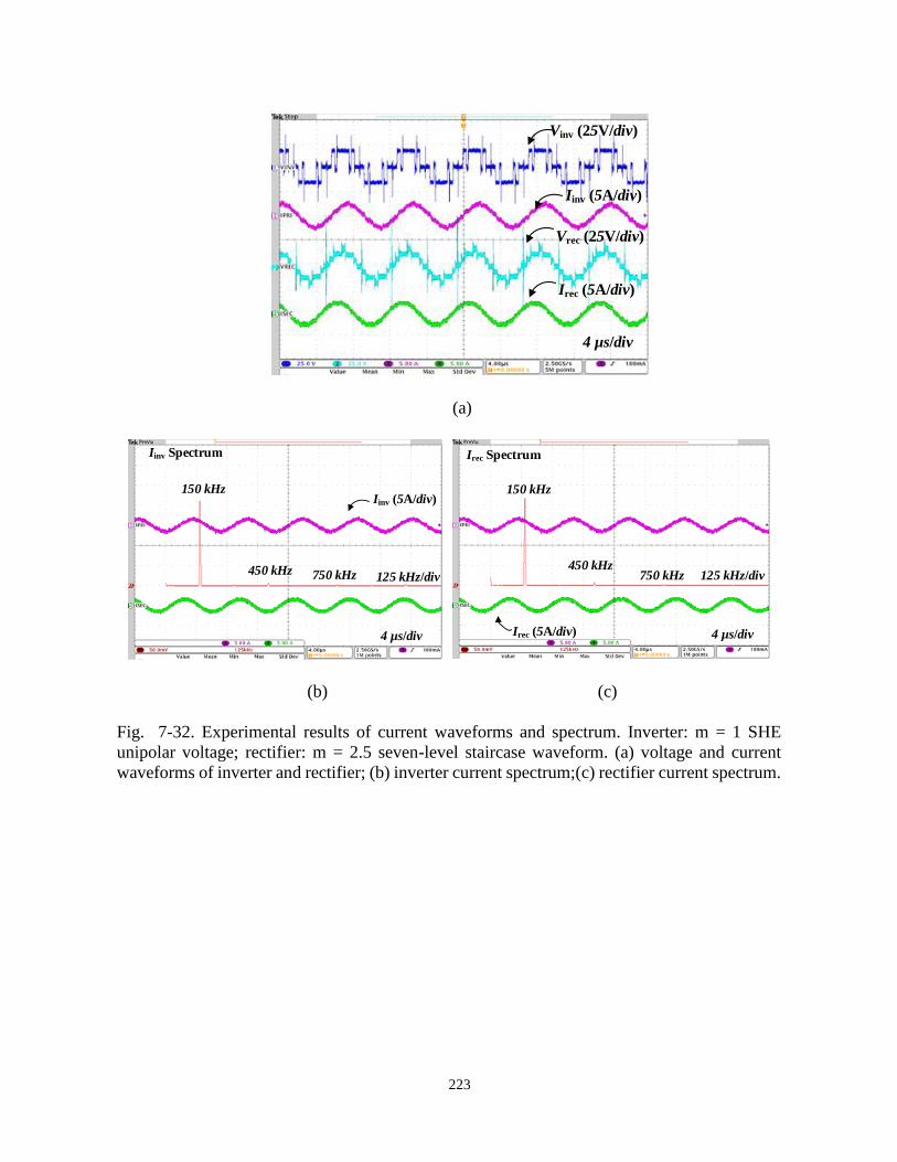
223
Vinv (25V/div)
Iinv (5A/div)
Vrec (25V/div)
Irec (5A/div)
4 µs/div
(a)
Iinv (5A/div)150 kHz
450 kHz 750 kHz
4 µs/div
125 kHz/div
Iinv Spectrum
Irec (5A/div)
150 kHz
450 kHz750 kHz
4 µs/div
125 kHz/div
Irec Spectrum
(b) (c)
Fig. 7-32. Experimental results of current waveforms and spectrum. Inverter: m = 1 SHE
unipolar voltage; rectifier: m = 2.5 seven-level staircase waveform. (a) voltage and current
waveforms of inverter and rectifier; (b) inverter current spectrum;(c) rectifier current spectrum.
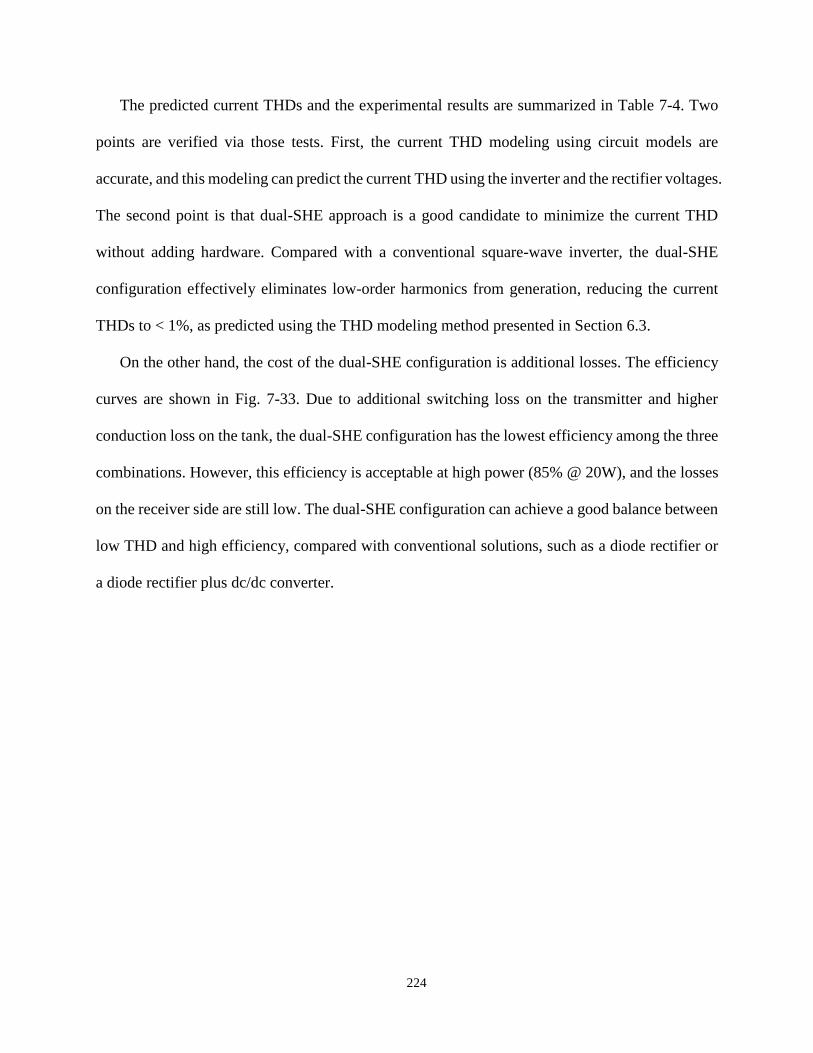
224
The predicted current THDs and the experimental results are summarized in Table 7-4. Two
points are verified via those tests. First, the current THD modeling using circuit models are
accurate, and this modeling can predict the current THD using the inverter and the rectifier voltages.
The second point is that dual-SHE approach is a good candidate to minimize the current THD
without adding hardware. Compared with a conventional square-wave inverter, the dual-SHE
configuration effectively eliminates low-order harmonics from generation, reducing the current
THDs to < 1%, as predicted using the THD modeling method presented in Section 6.3.
On the other hand, the cost of the dual-SHE configuration is additional losses. The efficiency
curves are shown in Fig. 7-33. Due to additional switching loss on the transmitter and higher
conduction loss on the tank, the dual-SHE configuration has the lowest efficiency among the three
combinations. However, this efficiency is acceptable at high power (85% @ 20W), and the losses
on the receiver side are still low. The dual-SHE configuration can achieve a good balance between
low THD and high efficiency, compared with conventional solutions, such as a diode rectifier or
a diode rectifier plus dc/dc converter.
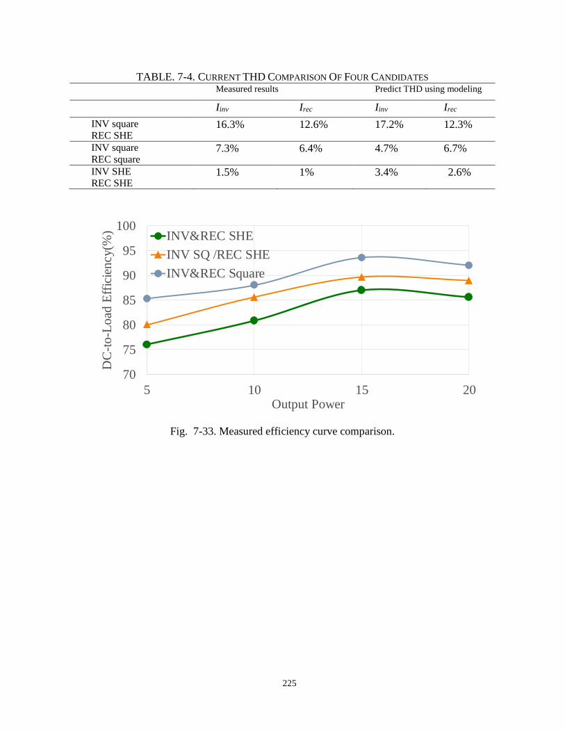
225
TABLE. 7-4. CURRENT THD COMPARISON OF FOUR CANDIDATES
Measured results Predict THD using modeling
Iinv Irec Iinv Irec
INV square
REC SHE 16.3% 12.6% 17.2% 12.3%
INV square
REC square 7.3% 6.4% 4.7% 6.7%
INV SHE
REC SHE 1.5% 1% 3.4% 2.6%
Fig. 7-33. Measured efficiency curve comparison.
70
75
80
85
90
95
100
5 10 15 20
DC
-to
-Load
Eff
icie
ncy(%
)
Output Power
INV&REC SHE
INV SQ /REC SHE
INV&REC Square
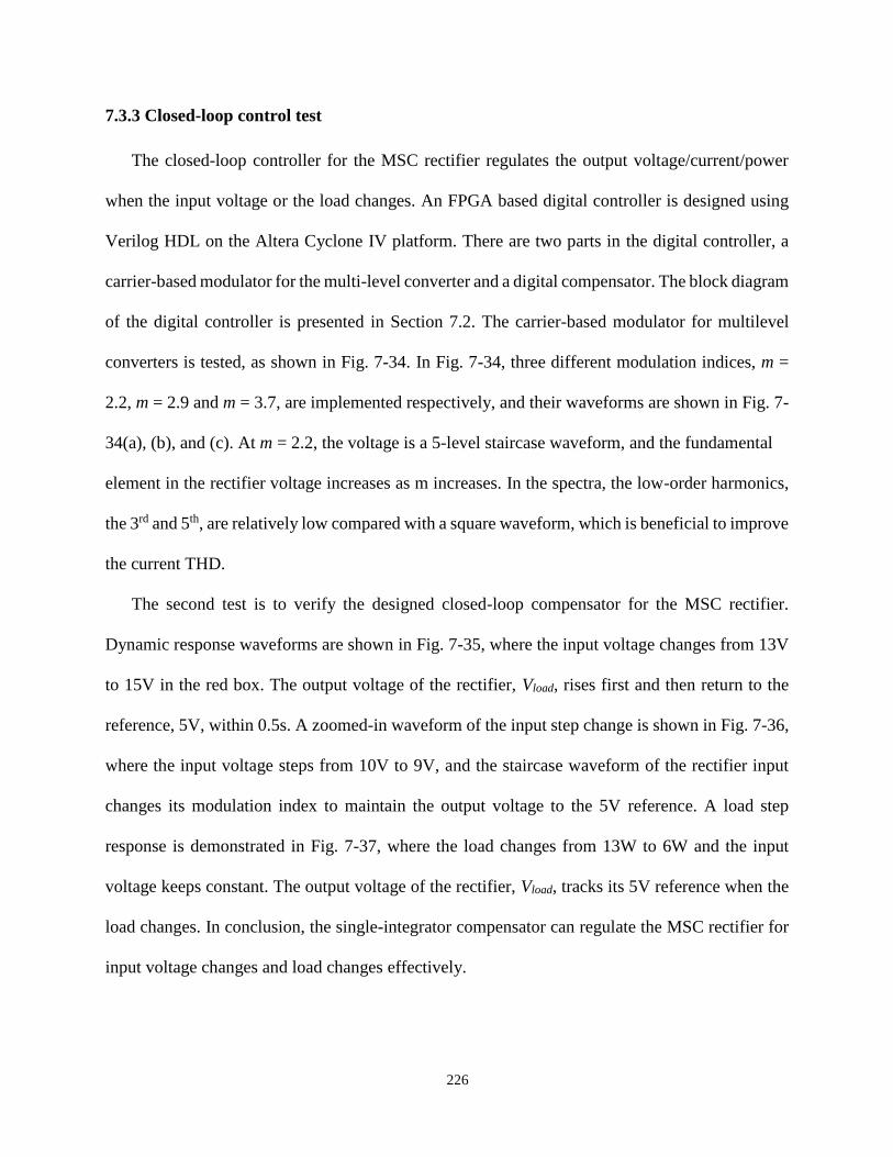
226
7.3.3 Closed-loop control test
The closed-loop controller for the MSC rectifier regulates the output voltage/current/power
when the input voltage or the load changes. An FPGA based digital controller is designed using
Verilog HDL on the Altera Cyclone IV platform. There are two parts in the digital controller, a
carrier-based modulator for the multi-level converter and a digital compensator. The block diagram
of the digital controller is presented in Section 7.2. The carrier-based modulator for multilevel
converters is tested, as shown in Fig. 7-34. In Fig. 7-34, three different modulation indices, m =
2.2, m = 2.9 and m = 3.7, are implemented respectively, and their waveforms are shown in Fig. 7-
34(a), (b), and (c). At m = 2.2, the voltage is a 5-level staircase waveform, and the fundamental
element in the rectifier voltage increases as m increases. In the spectra, the low-order harmonics,
the 3rd and 5th, are relatively low compared with a square waveform, which is beneficial to improve
the current THD.
The second test is to verify the designed closed-loop compensator for the MSC rectifier.
Dynamic response waveforms are shown in Fig. 7-35, where the input voltage changes from 13V
to 15V in the red box. The output voltage of the rectifier, Vload, rises first and then return to the
reference, 5V, within 0.5s. A zoomed-in waveform of the input step change is shown in Fig. 7-36,
where the input voltage steps from 10V to 9V, and the staircase waveform of the rectifier input
changes its modulation index to maintain the output voltage to the 5V reference. A load step
response is demonstrated in Fig. 7-37, where the load changes from 13W to 6W and the input
voltage keeps constant. The output voltage of the rectifier, Vload, tracks its 5V reference when the
load changes. In conclusion, the single-integrator compensator can regulate the MSC rectifier for
input voltage changes and load changes effectively.
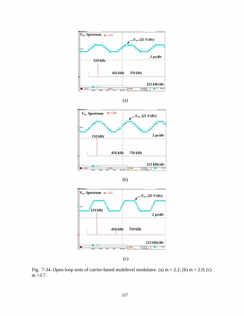
227
150 kHz
450 kHz 750 kHz
125 kHz/div
Vrec (25 V/div)
2 µs/div
Vrec Spectrum m = 2.2
(a)
150 kHz
450 kHz 750 kHz
125 kHz/div
Vrec (25 V/div)
2 µs/div
Vrec Spectrum m = 2.9
(b)
150 kHz
450 kHz 750 kHz
125 kHz/div
Vrec (25 V/div)
2 µs/div
Vrec Spectrum m = 3.7
(c)
Fig. 7-34. Open-loop tests of carrier-based multilevel modulator. (a) m = 2.2; (b) m = 2.9; (c)
m =3.7.
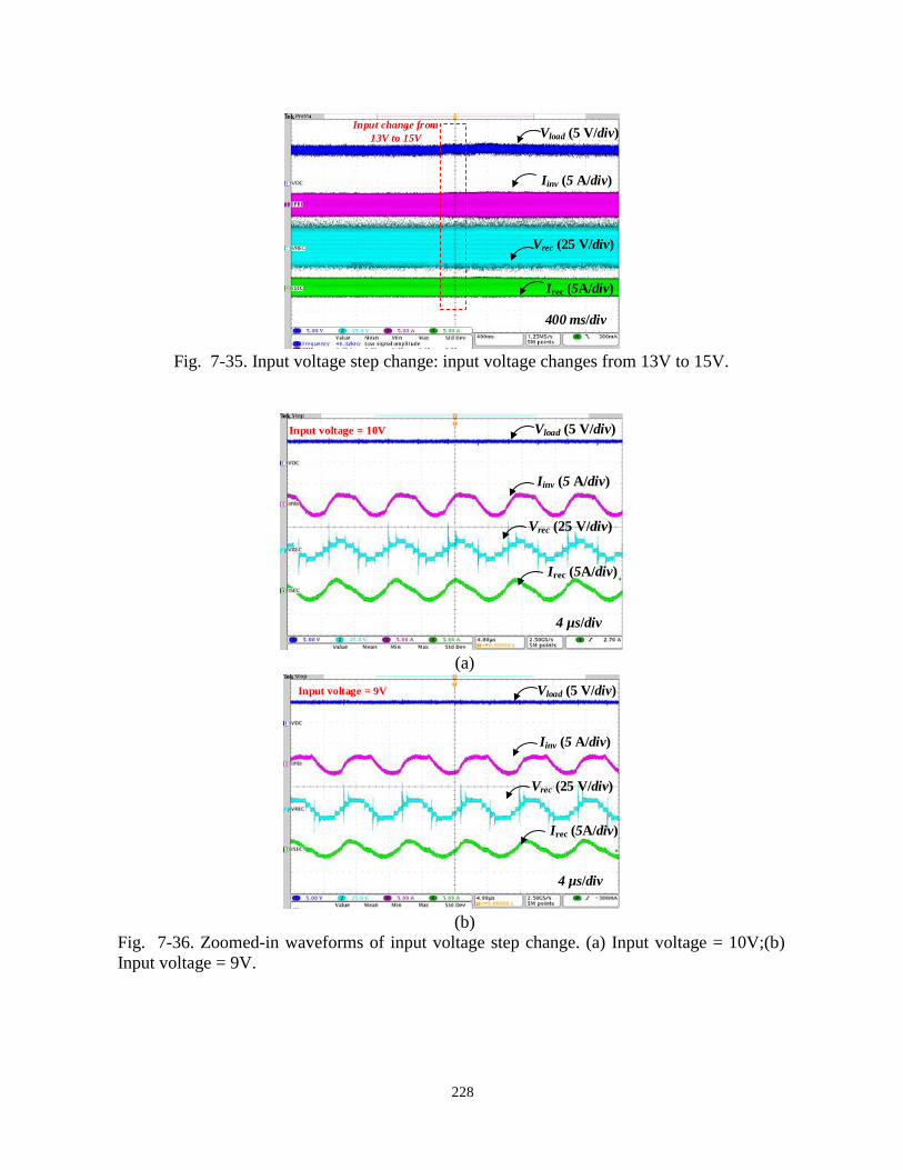
228
Vload (5 V/div)
Vrec (25 V/div)
Iinv (5 A/div)
400 ms/div
Irec (5A/div)
Input change from
13V to 15V
Fig. 7-35. Input voltage step change: input voltage changes from 13V to 15V.
Vrec (25 V/div)
Iinv (5 A/div)
Irec (5A/div)
Vload (5 V/div)
4 µs/div
Input voltage = 10V
(a)
Vrec (25 V/div)
Iinv (5 A/div)
Irec (5A/div)
Vload (5 V/div)
4 µs/div
Input voltage = 9V
(b)
Fig. 7-36. Zoomed-in waveforms of input voltage step change. (a) Input voltage = 10V;(b)
Input voltage = 9V.
229
Vload (5 V/div)
Vrec (25 V/div)
Iinv (5 A/div)
400 ms/div
Irec (5A/div)
Load change from
13W to 6W
Fig. 7-37. Load step change: load changes from 13W to 6W.
230
8. Conclusion and Future Work
8.1 Conclusion
In this dissertation, the multi-frequency modulation and control for dc/ac and ac/dc resonant
converters are systematically investigated, which reduces the safety concerns, leverages combined
functionalities and improves the conversion efficiency, THD and power density of the targeted
applications. Conventional approach to reduce the harmonic content in resonant converters is by
means of passive filters. In this work, a modulation and control-based methodology is proposed
for two representative applications, electrosurgical generator and wireless power transfer system.
Conventional programmed PWM is widely used in line-frequency applications, with a single-
frequency generation ability. In this dissertation, three multi-frequency programmed pulse-width
modulations (MFPWM) (unipolar, bipolar and phase-shift) are proposed, which simultaneously
generate two frequencies while eliminating undesired low-order harmonics in between. The
proposed MFPWM enables multi-output, high-frequency, low-harmonic resonant converter
applications, reducing semiconductor device and passive filter count.
Three metrics to evaluate MFPWM (modulation range, switching loss and harmonic content)
are investigated and compared with benchmark evaluations. To enable widely separated frequency
generation and flexible combination, extension studies of MFPWM are included. The MFPWM
supports dual-frequency generation across over 30 harmonics, and a generation of multiple
harmonics for more than 2 outputs. Conventional programmed PWM only control a total number
of harmonics fewer than 15. This extension study makes MFPWM applicable to multi-output,
frequency widely-separated applications,
The multilevel MFPWM is briefly discussed, but its application is limited by the narrow
modulation range of HF. A full solution of the MFPWM problem is studied using a polynomial-
231
base algorithm. The unipolar and bipolar MFPWM have only one solution set, but the phase-shift
MFPWM has two sets. The multiple solutions of MFPWM is useful, because the additional
solution sets may improve THD compared with the original one.
When selecting MFPWM among the three, the modulation range of LF and HF, the switching
loss and the harmonic content beyond the controllable range are different. The unipolar MFPWM
has a constrained range of LF and HF due to the unipolar contour but has low harmonic content
and the lowest switching loss of the three. This feature makes the unipolar MFPWM a good
candidate for applications like ESG, which emphasizes safety and accuracy, rather than a wide
range regulation ability. The bipolar MFPWM has extended modulation range but poor harmonic
content due to 2Vdc voltage swing at the switching transition. This is suitable for the dual-mode
WPT application where a fast and wide regulation ability is priority. The phase-shift MFPWM
achieves a good balance between the modulation range and the harmonic content and is suitable
for both cases. However, the phase-shift MFPWM cannot utilize the triplen harmonics as an output,
which restrains its application if a specific frequency combination is required. The design and
implementation of an ESG and a dual-mode WPT transmitter prototypes are demonstrated, and
the experimental results verify the effectiveness of the proposed MFPWM schemes.
Due to space constraints on mobile devices, thermal dissipation area and passive filters are
strictly limited for WPT receivers, and it proposes a challenge for wireless fast charging on mobile
devices. A new WPT receiver architecture is proposed in this dissertation to overcome the
challenges of constraints on thermal, efficiency and power density, leveraging the multi-frequency
modulation and control method. The proposed multilevel switched-capacitor rectifier (MSC)
features a multilevel staircase waveform, eliminating significant low-order harmonics from
generation, and avoids bulky passive filters. In addition, the new architecture has a combined
232
voltage-step down ability, reducing the major conduction loss in the WPT receiver on both coil
and rectifier. Finally, the high energy-density switched capacitor circuit facilitates integrated
circuit design, improving the power density. The proposed WPT receiver is evaluated and
compared with the state-of-the-art technologies, regarding the regulation ability, conversion
efficiency, current THD and power density. This comparison demonstrates advantages of the
proposed MSC rectifier regarding the four metrics, providing a new perspective designing ac/dc
rectifier for wireless fast charging applications
The loss modeling of the MSC rectifier is investigated and verified on a 20 W porotype. Two
charge control schemes and a multilevel modulation scheme are proposed for the MSC rectifier.
The proposed charge control schemes reduce the charge sharing loss of the MSC rectifier when
the phase-shift control is employed in WPT system. The multilevel modulation scheme helps the
MSC rectifier to achieve low harmonic content, which is not addressed in previous research.
The device sizing for the IC implementation of the MSC rectifier is investigated. The charge
sharing loss of the MSC rectifier is modeled using the equivalent output impedance, which helps
the device sizing for this topology. Techniques and trade-offs, which include changing flying
capacitance and the operating frequency, to further reduce the charge sharing loss of the MSC
rectifier are discussed, which provide more options to optimize the die area and the efficiency.
The multilevel converter modulator and closed-loop design of the MSC rectifier for battery
charging are demonstrated in this dissertation. A full GaN-based, 7-level, 150 kHz prototype is
built. The loss modeling, current THD modeling and the closed-loop design of the MSC rectifier
are verified on the prototype. A peak 94% system efficiency and 97% rectifier stage efficiency are
achieved. The best current THD of the prototype is less than 1%, and the rectifier volume is
233
estimated. Compared to the state-of-the-art technologies, the experimental results and the analysis
prove that the MSC is an excellent candidate for fast wireless charging applications.
8.2 Future work
In the future, several works can enhance the research of the multi-frequency generation and
control for dc/ac and ac/dc resonant converters.
The MFPWM problem now is discretely calculated using Matlab in this dissertation, and it is
burdensome process for electrical engineers. A universal software tool calculates the
transcendental equations of MFPWM problems save time for individual coding for each problem.
A software that packages solving algorithms and displays engineer-friendly interface is beneficial
for research in this field.
In the ESG implementation, a pre-regulation dc/dc stage helps to extend the control range of
the multi-mode inverter. A control guideline is developed in this dissertation, and a detailed
implementation is a step further to fulfil the production of such multi-mode ESGs.
The MSC rectifier may suffer from the charge sharing loss at light load. a charge sharing loss
reduction is conceptualized in this dissertation with simulation results. A systematic study for
light-load efficiency improvement of the MSC rectifier is advantageous.
The new WPT fast charging architecture featuring MSC rectifier reduces the conduction by
configuring a high-voltage, low-current power transfer path. As a result, the transmitter requires a
voltage step-up ability so that the MSC rectifier can step it down to the low-voltage battery.
Conventional solutions use a pre-regulation Boost converter to provide the voltage step-up ability,
and a full bridge inverter generates a square waveform. However, the MSC inverter, the dual of
the MSC rectifier, is a good candidate. The MSC inverter has voltage step-up ability, generating
low harmonic content due to multilevel waveforms. In the preliminary simulation, the dual-MSC

234
WPT system shows the lowest current THD among all combinations, which further improves the
performance of the wireless fast charging system.

235
List of Reference
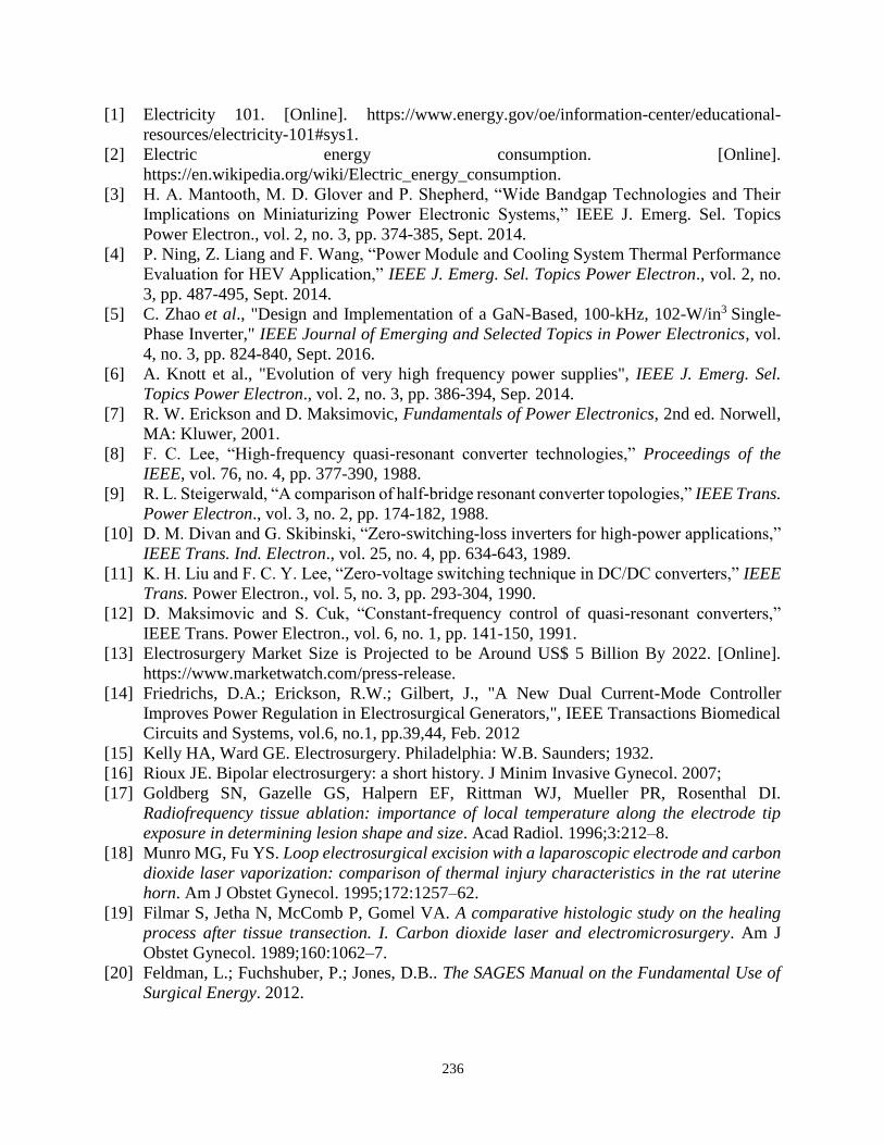
236
[1] Electricity 101. [Online]. https://www.energy.gov/oe/information-center/educational-
resources/electricity-101#sys1.
[2] Electric energy consumption. [Online].
https://en.wikipedia.org/wiki/Electric_energy_consumption.
[3] H. A. Mantooth, M. D. Glover and P. Shepherd, “Wide Bandgap Technologies and Their
Implications on Miniaturizing Power Electronic Systems,” IEEE J. Emerg. Sel. Topics
Power Electron., vol. 2, no. 3, pp. 374-385, Sept. 2014.
[4] P. Ning, Z. Liang and F. Wang, “Power Module and Cooling System Thermal Performance
Evaluation for HEV Application,” IEEE J. Emerg. Sel. Topics Power Electron., vol. 2, no.
3, pp. 487-495, Sept. 2014.
[5] C. Zhao et al., "Design and Implementation of a GaN-Based, 100-kHz, 102-W/in3 Single-
Phase Inverter," IEEE Journal of Emerging and Selected Topics in Power Electronics, vol.
4, no. 3, pp. 824-840, Sept. 2016.
[6] A. Knott et al., "Evolution of very high frequency power supplies", IEEE J. Emerg. Sel.
Topics Power Electron., vol. 2, no. 3, pp. 386-394, Sep. 2014.
[7] R. W. Erickson and D. Maksimovic, Fundamentals of Power Electronics, 2nd ed. Norwell,
MA: Kluwer, 2001.
[8] F. C. Lee, “High-frequency quasi-resonant converter technologies,” Proceedings of the
IEEE, vol. 76, no. 4, pp. 377-390, 1988.
[9] R. L. Steigerwald, “A comparison of half-bridge resonant converter topologies,” IEEE Trans.
Power Electron., vol. 3, no. 2, pp. 174-182, 1988.
[10] D. M. Divan and G. Skibinski, “Zero-switching-loss inverters for high-power applications,”
IEEE Trans. Ind. Electron., vol. 25, no. 4, pp. 634-643, 1989.
[11] K. H. Liu and F. C. Y. Lee, “Zero-voltage switching technique in DC/DC converters,” IEEE
Trans. Power Electron., vol. 5, no. 3, pp. 293-304, 1990.
[12] D. Maksimovic and S. Cuk, “Constant-frequency control of quasi-resonant converters,”
IEEE Trans. Power Electron., vol. 6, no. 1, pp. 141-150, 1991.
[13] Electrosurgery Market Size is Projected to be Around US$ 5 Billion By 2022. [Online].
https://www.marketwatch.com/press-release.
[14] Friedrichs, D.A.; Erickson, R.W.; Gilbert, J., "A New Dual Current-Mode Controller
Improves Power Regulation in Electrosurgical Generators,", IEEE Transactions Biomedical
Circuits and Systems, vol.6, no.1, pp.39,44, Feb. 2012
[15] Kelly HA, Ward GE. Electrosurgery. Philadelphia: W.B. Saunders; 1932.
[16] Rioux JE. Bipolar electrosurgery: a short history. J Minim Invasive Gynecol. 2007;
[17] Goldberg SN, Gazelle GS, Halpern EF, Rittman WJ, Mueller PR, Rosenthal DI.
Radiofrequency tissue ablation: importance of local temperature along the electrode tip
exposure in determining lesion shape and size. Acad Radiol. 1996;3:212–8.
[18] Munro MG, Fu YS. Loop electrosurgical excision with a laparoscopic electrode and carbon
dioxide laser vaporization: comparison of thermal injury characteristics in the rat uterine
horn. Am J Obstet Gynecol. 1995;172:1257–62.
[19] Filmar S, Jetha N, McComb P, Gomel VA. A comparative histologic study on the healing
process after tissue transection. I. Carbon dioxide laser and electromicrosurgery. Am J
Obstet Gynecol. 1989;160:1062–7.
[20] Feldman, L.; Fuchshuber, P.; Jones, D.B.. The SAGES Manual on the Fundamental Use of
Surgical Energy. 2012.
237
[21] Wireless Power Consortium. “The Qi wireless power transfer system power class 0
specification”. [Online]. Available: https://www.wirelesspowerconsortium.com/
[22] Airfuel Alliance. “The Airfuel Alliance Specification”. [Online]. Available:
https://www.airfuel.org.
[23] J. C. Schuder, H. E. Stephenson. “Energy transport to a coil which circumscribes a ferrite
core and is implanted within the body”. IEEE Trans. Bio-Med. Eng. vol. 12, no. 3 and 4,
pp.154-163, 1965.
[24] S.Y.R.Hui, Wing. W. C. Ho,"A new generation of universal contactless battery charging
platform for portable consumer electronic equipment", IEEE Trans. Power Electron., vol.20,
no.3,pp 620 – 627,May 2005
[25] S. Y. Hui, "Planar wireless charging technology for portable electronic products and Qi,"
Proceedings of the IEEE, vol. 101, no.6, pp. 1290-1301, Jun. 2013.
[26] R. Tseng, B. von Novak, S. Shevde, K.A. Grajski, "Introduction to the alliance for wireless
power loosely-coupled wireless power transfer system specification version 1.0", Proc. IEEE
Wireless Power Transfer (WPT), Perugia, Italy, May 2013, pp79 – 83.
[27] M. Yilmaz and P. T. Krein, "Review of battery charger topologies, charging power levels,
and infrastructure for plug-in electric and hybrid vehicles," IEEE Trans. Power Electron.,
vol. 28, no.5, pp. 2151-2169, May 2013.
[28] J. Sallan, J. L. Villa, A. Llombart, and J. F. Sanz, "Optimal design of ICPT systems applied
to electric vehicle battery charge," IEEE Trans. Ind. Electron., vol. 56, no.6, pp. 2140-2149,
Jun. 2009.
[29] M. Budhia, J. T. Boys, G. A. Covic, and C. Huang, "Development of a single-sided flux
magnetic coupler for electric vehicle IPT charging systems", IEEE Trans. Power Electron.,
vol. 60, no.1, pp318-328, Jan. 2013.
[30] S. Chopra and P. Bauer, "Driving range extension of EV with on-road contactless power
transfer: A case study," IEEE Trans. Ind. Electron., vol. 60, no.1, pp. 329-338, Jan. 2013.
[31] U. K. Madawala and D. J. Thrimawithana, "A bidirectional inductive power interface for
electric vehicles in V2G systems," IEEE Trans. Ind. Electron., vol. 58, no.10, pp. 4789-4796,
Oct. 2011.
[32] S. Ping, A. P. Hu, S. Malpas, and D. Budgett, "A frequency control method for regulating
wireless power to implantable devices," IEEE Trans. Biomedical Circuits and Systems, vol.
2, no.1, pp. 22-29, Mar. 2008.
[33] V. J. Brusamarello, Y. B. Blauth, R. de Azambuja, I. Muller, and F. R. de Sousa, "Power
transfer with an inductive link and wireless tuning," IEEE Trans. Instrumentation and
Measurement, vol. 62, no.5, pp. 924-931, May 2013.
[34] R. Johari, J. V. Krogmeier and D. J. Love, "Analysis and practical considerations in
implementing multiple transmitters for wireless power transfer via coupled magnetic
resonance," IEEE Trans. Ind. Electron., vol. 61, no.4, pp. 1774-1783, Apr. 2014.
[35] F. van der Pijl, P. Bauer and M. Castilla, "Control method for wireless inductive energy
transfer systems with relatively large air gap," IEEE Trans. Ind. Electron., vol. 60, no.1, pp.
382-390, Jan. 2013.
[36] T. A. Lipo and D. G. Holmes, Pulse-Width Modulation for Power Converters Principles and
Practice. Piscataway, NJ, USA: IEEE Press, 2003.
[37] J. Holtz, "Pulsewidth modulation for electronic power conversion," Proceedings of the IEEE,
vol. 82, no. 8, pp. 1194-1214, Aug 1994.
238
[38] B.K. Bose, Power electronics and variable frequency drives: technology and applications.
Upper Saddle River, NJ: Prentice-Hall PTR, 2002.
[39] H. S. Patel and R. G. Hoft, “Generalized techniques of harmonic elimination and voltage
control in thyristor inverters: Part I—harmonic elimination,” IEEE Trans. Ind. Appl., vol.
IA-9, no. 3, pp. 310–317, May/Jun. 1973.
[40] M. S. A. Dahidah, G. Konstantinou and V. G. Agelidis, "A Review of Multilevel Selective
Harmonic Elimination PWM: Formulations, Solving Algorithms, Implementation and
Applications," IEEE Transactions Power Electronics, vol. 30, no. 8, pp. 4091-4106, Aug.
2015.
[41] A. M. Hava, R. J. Kerkman and T. A. Lipo, "Simple analytical and graphical methods for
carrier-based PWM-VSI drives," IEEE Transactions Power Electronics, vol. 14, no. 1, pp.
49-61, Jan 1999.
[42] M. A. Boost and P. D. Ziogas, "State-of-the-art carrier PWM techniques: a critical
evaluation," IEEE Transactions Industry Applications, vol. 24, no. 2, pp. 271-280, Mar/Apr
1988.
[43] G. Fedele and D. Frascino, "Spectral Analysis of a Class of DC–AC PWM Inverters by
Kapteyn Series," IEEE Transactions Power Electronics, vol. 25, no. 4, pp. 839-849, April
2010
[44] J. Holtz and L. Springob, "Reduced harmonics PWM controlled line-side converter for
electric drives," IEEE Transactions Industry Applications, vol. 29, no. 4, pp. 814-819,
Jul/Aug 1993.
[45] Keliang Zhou and Danwei Wang, "Relationship between space-vector modulation and three-
phase carrier-based PWM: a comprehensive analysis [three-phase inverters]," IEEE
Transactions Industrial Electronics, vol. 49, no. 1, pp. 186-196, Feb 2002.
[46] H. W. van der Broeck, H. C. Skudelny and G. V. Stanke, "Analysis and realization of a
pulsewidth modulator based on voltage space vectors," IEEE Transactions Industry
Applications, vol. 24, no. 1, pp. 142-150, Jan/Feb 1988.
[47] T. G. Habetler, F. Profumo, M. Pastorelli and L. M. Tolbert, "Direct torque control of
induction machines using space vector modulation," IEEE Transactions Industry
Applications, vol. 28, no. 5, pp. 1045-1053, Sep/Oct 1992.
[48] Fei Wang, "Sine-triangle versus space-vector modulation for three-level PWM voltage-
source inverters," IEEE Transactions Industry Applications, vol. 38, no. 2, pp. 500-506,
Mar/Apr 2002.
[49] B. P. McGrath, D. G. Holmes and T. Lipo, "Optimized space vector switching sequences for
multilevel inverters," IEEE Transactions Power Electronics, vol. 18, no. 6, pp. 1293-1301,
Nov. 2003.
[50] H. Fujita and H. Akagi, “Pulse-density-modulated power control of a 4 kW 450 kHz voltage-
source inverter for induction melting applications,” IEEE Trans. Industrial Appl., vol. 32,
no. 2, pp. 279–286, Mar./Apr. 1996.
[51] ] S. Mollov, M. Theodoridis, and A. Forsyth, “High frequency voltage-fed inverter with
phase-shift control for induction heating,” Proc. Inst. Elect. Eng.—Electr. Power Appl., Jan.
2004, vol. 151, no. 1, pp. 12–18.
[52] L. A. Barragán, D. Navarro, J. Acero, I. Urriza, and J. M. Burdío, “FPGA implementation of
a switching frequency modulation circuit for EMI reduction in resonant inverters for
induction heating appliances,” IEEE Trans. Ind. Electron., vol. 55, no. 1, pp. 11–20, Jan.
2008
239
[53] T. G. Habetler, R. Naik and T. A. Nondahl, "Design and implementation of an inverter output
LC filter used for dv/dt reduction," IEEE Transactions Power Electronics, vol. 17, no. 3, pp.
327-331, May 2002.
[54] C. Lascu, L. Asiminoaei, I. Boldea and F. Blaabjerg, "High Performance Current Controller
for Selective Harmonic Compensation in Active Power Filters," IEEE Transactions Power
Electronics, vol. 22, no. 5, pp. 1826-1835, Sept. 2007.
[55] S. Fukuda, M. Ohta and Y. Iwaji, "An Auxiliary-Supply-Assisted Harmonic Reduction
Scheme for 12-Pulse Diode Rectifiers," IEEE Transactions Power Electronics, vol. 23, no.
3, pp. 1270-1277, May 2008.
[56] D. M. Divan and T. H. Barton, "Harmonic Reduction in Synchronous Chopper-Converter
Combinations," IEEE Transactions Industry Applications, vol. IA-21, no. 2, pp. 382-390,
March 1985.
[57] M. Rastogi, R. Naik and N. Mohan, "A comparative evaluation of harmonic reduction
techniques in three-phase utility interface of power electronic loads," IEEE Transactions
Industry Applications, vol. 30, no. 5, pp. 1149-1155, Sep/Oct 1994.
[58] T. G. Habetler and D. M. Divan, "Acoustic noise reduction in sinusoidal PWM drives using
a randomly modulated carrier," IEEE Transactions Power Electronics, vol. 6, no. 3, pp. 356-
363, Jul 1991.
[59] K. K. Tse, H. S. H. Chung, S. Y. Huo and H. C. So, "Analysis and spectral characteristics of
a spread-spectrum technique for conducted EMI suppression," IEEE Transactions Power
Electronics, vol. 15, no. 2, pp. 399-410, Mar 2000.
[60] J. Rodriguez, Jih-Sheng Lai and Fang Zheng Peng, "Multilevel inverters: a survey of
topologies, controls, and applications," IEEE Transactions on Industrial Electronics, vol. 49,
no. 4, pp. 724-738, Aug 2002.
[61] M. S. A. Dahidah and V. G. Agelidis, "Selective Harmonic Elimination PWM Control for
Cascaded Multilevel Voltage Source Converters: A Generalized Formula," IEEE
Transactions Power Electronics, vol. 23, no. 4, pp. 1620-1630, July 2008.
[62] L. G. Franquelo, J. Napoles, R. C. P. Guisado, J. I. Leon and M. A. Aguirre, "A Flexible
Selective Harmonic Mitigation Technique to Meet Grid Codes in Three-Level PWM
Converters," IEEE Transactions Industrial Electronics, vol. 54, no. 6, pp. 3022-3029, Dec.
2007.
[63] W. Fei, X. Du and B. Wu, "A Generalized Half-Wave Symmetry SHE-PWM Formulation
for Multilevel Voltage Inverters," IEEE Transactions Industrial Electronics, vol. 57, no. 9,
pp. 3030-3038, Sept. 2010.
[64] L. M. Tolbert, Fang Zheng Peng and T. G. Habetler, "Multilevel converters for large electric
drives," IEEE Transactions Industry Applications, vol. 35, no. 1, pp. 36-44, Jan/Feb 1999.
[65] Z. Du, L. M. Tolbert, B. Ozpineci and J. N. Chiasson, "Fundamental Frequency Switching
Strategies of a Seven-Level Hybrid Cascaded H-Bridge Multilevel Inverter," IEEE
Transactions Power Electronics, vol. 24, no. 1, pp. 25-33, Jan. 2009.
[66] J. R. Wells, B. M. Nee, P. L. Chapman and P. T. Krein, "Selective harmonic control: a general
problem formulation and selected solutions," IEEE Transactions Power Electronics, vol. 20,
no. 6, pp. 1337-1345, Nov. 2005.
[67] P. N. Enjeti, P. D. Ziogas, and J. F. Lindsay, “Programmed PWM techniques to eliminate
harmonics: A critical evaluation,” IEEE Trans. Ind. Appl., vol. 26, no. 2, pp. 302–316,
Mar./Apr. 1990.
240
[68] M. S. A. Dahidah, G. Konstantinou, N. Flourentzou, and V. G. Agelidis,”On comparing the
symmetrical and non-symmetrical selective harmonic elimination pulse-width modulation
technique for two-level three-phase voltage source converters,” IET Power Electron., vol. 3,
pp. 829–842, 2010.
[69] P. Enjeti and J. F. Lindsay, “Solving nonlinear equations of harmonic elimination PWM in
power control,” IEE Electron. Lett., vol. 23, no. 12, pp. 656–657, Jun. 1987.
[70] J. Sun, S. Beineke, and H.Grotstollen, “Optimal PWMbased on real-time solution of
harmonic elimination equations,” IEEE Trans. Ind. Electron.,vol. 11, no. 4, pp. 612–621, Jul.
1996.
[71] J.-W. Chen, T. J. Liang, and S. H.Wang, “A novel design and implementation of
programmed PWM to eliminated harmonics,” Proc. IEEE Int. Conf. Ind. Electron. Control
Instrum. Autom., Raleigh, NC, USA, Nov. 6–10, 2005, pp. 1278–1283.
[72] D. Ahmadi, K. Zou, C. Li, Y. Huang and J. Wang, "A Universal Selective Harmonic
Elimination Method for High-Power Inverters," IEEE Transactions Power Electronics, vol.
26, no. 10, pp. 2743-2752, Oct. 2011.
[73] R. Pindado, C. Jaen and J. Pou, "Robust method for optimal PWM harmonic elimination
based on the Chebyshev functions," Proceedings of 8th International Conference on
Harmonics and Quality of Power., Athens, 1998, pp. 976-981 vol.2.
[74] T. J. Liang, R. M. O’Connell, and R. G. Hoft, “Inverter harmonic reduction using Walsh
function harmonic elimination method,” IEEE Trans. Power Electron., vol. 12, no. 6, pp.
971–982, Nov.1997.
[75] J. N. Chiasson, L. M. Tolbert, K. J. McKenzie and Zhong Du, "A complete solution to the
harmonic elimination problem," IEEE Transactions Power Electronics, vol. 19, no. 2, pp.
491-499, March 2004.
[76] J. N. Chiasson, L. M. Tolbert, K. J. McKenzie and Zhong Du, "Control of a multilevel
converter using resultant theory," IEEE Transactions Control Systems Technology, vol. 11,
no. 3, pp. 345-354, May 2003.
[77] L. M. Tolbert, J. N. Chiasson, Zhong Du and K. J. McKenzie, "Elimination of harmonics in
a multilevel converter with nonequal DC sources," IEEE Transactions Industry Applications,
vol. 41, no. 1, pp. 75-82, Jan.-Feb. 2005.
[78] K. Yang, Z. Yuan, R. Yuan, W. Yu, J. Yuan and J. Wang, "A Groebner Bases Theory-Based
Method for Selective Harmonic Elimination," IEEE Transactions Power Electronics, vol.
30, no. 12, pp. 6581-6592, Dec. 2015.
[79] V. G. Agelidis, A. Balouktsis, I. Balouktsis and C. Cossar, "Multiple sets of solutions for
harmonic elimination PWM bipolar waveforms: analysis and experimental verification,"
IEEE Transactions Power Electronics, vol. 21, no. 2, pp. 415-421, March 2006.
[80] A. Kavousi, B. Vahidi, R. Salehi, M. K. Bakhshizadeh, N. Farokhnia and S. H. Fathi,
"Application of the Bee Algorithm for Selective Harmonic Elimination Strategy in
Multilevel Inverters," IEEE Transactions Power Electronics, vol. 27, no. 4, pp. 1689-1696,
April 2012.
[81] B. Ozpineci, L. M. Tolbert and J. N. Chiasson, "Harmonic optimization of multilevel
converters using genetic algorithms," IEEE Power Electronics Letters, vol. 3, no. 3, pp. 92-
95, Sept. 2005.
[82] F. Filho, L. M. Tolbert, Y. Cao and B. Ozpineci, "Real-Time Selective Harmonic
Minimization for Multilevel Inverters Connected to Solar Panels Using Artificial Neural
241
Network Angle Generation," IEEE Transactions Industry Applications, vol. 47, no. 5, pp.
2117-2124, Sept.-Oct. 2011.
[83] Fujita, H.; Uchida, N.; Ozaki, K., "A New Zone-Control Induction Heating System Using
Multiple Inverter Units Applicable Under Mutual Magnetic Coupling Conditions,", IEEE
Transactions Power Electronics, vol.26, no.7, pp.2009,2017, July 2011
[84] Esteve, V.; Jordán, J.; Sanchis-Kilders, E.; Dede, E.J.; Maset, E.; Ejea, J.B.; Ferreres, A.,
"Comparative Study of a Single Inverter Bridge for Dual-Frequency Induction Heating Using
Si and SiC MOSFETs,", IEEE Transactions Industrial Electronics, vol.62, no.3,
pp.1440,1450, March 2015
[85] Papani, S.K.; Neti, V.; Murthy, B.K., "Dual frequency inverter configuration for multiple-
load induction cooking application," IET Power Electronics, vol.8, no.4, pp.591,601, 4 2015
[86] Hirokawa, T.; Hiraki, E.; Tanaka, T.; Imai, M.; Yasui, K.; Sumiyoshi, S., "Dual-frequency
multiple-output resonant soft-switching inverter for induction heating cooking appliances,"
Industrial Electronics Society, IEEE IECON 2013 - 39th Annual Conference, vol., no.,
pp.5028,5033, 10-13 Nov. 2013
[87] Pantic, Z.; Lee, K.; Lukic, S.M., "Receivers for Multifrequency Wireless Power Transfer:
Design for Minimum Interference,", IEEE Journal of Emerging and Selected Topics in
Power Electronics, vol.3, no.1, pp.234,241, March 2015
[88] Y. Zhang, et al., "Selective Wireless Power Transfer to Multiple Loads Using Receivers of
Different Resonant Frequencies," IEEE Trans. Power Electron., vol. 30, no. 11, pp. 6001-
6005, Nov. 2015.
[89] M. Q. Nguyen, et al., "Multiple-Inputs and Multiple-Outputs Wireless Power Combining and
Delivering Systems," IEEE Trans. Power Electron., vol. 30, no. 11, pp. 6254-6263, Nov.
2015.
[90] Y. J. Kim, D. Ha, W. J. Chappell and P. P. Irazoqui, "Selective Wireless Power Transfer for
Smart Power Distribution in a Miniature-Sized Multiple-Receiver System," IEEE Trans.
Industrial Electron, vol. 63, no. 3, pp. 1853-1862, March 2016.
[91] W. Zhong et al., "Auxiliary Circuits for Power Flow Control in Multifrequency Wireless
Power Transfer Systems with Multiple Receivers," IEEE Trans. Power Electron., vol. 30,
no. 10, pp. 5902-5910, Oct. 2015.
[92] K. E. Koh, T. C. Beh, T. Imura and Y. Hori, "Impedance Matching and Power Division Using
Impedance Inverter for Wireless Power Transfer via Magnetic Resonant Coupling," IEEE
Trans. Industry Application., vol. 50, no. 3, pp. 2061-2070, May-June 2014.
[93] J. Wu, C. Zhao. et al., "Wireless Power and Data Transfer via a Common Inductive Link
Using Frequency Division Multiplexing," IEEE Trans. Industrial Electron., vol. 62, no. 12,
pp. 7810-7820, Dec. 2015.
[94] D. Ahn and P. P. Mercier, "Wireless Power Transfer with Concurrent 200-kHz and 6.78-
MHz Operation in a Single-Transmitter Device," IEEE Trans Power Electron., vol. 31, no.
7, pp. 5018-5029, July 2016.
[95] P. S. Riehl, et al., "Wireless Power Systems for Mobile Devices Supporting Inductive and
Resonant Operating Modes," IEEE Trans. Microwave Theory and Tech., vol. 63, no. 3, pp.
780-790, March 2015.
[96] M. d. Rooij and Y. Zhang, "A 10 W Multi-Mode Capable Wireless Power Amplifier for
Mobile Devices," International Exhibition and Conference for Power Electronics, Intelligent
Motion, Renewable Energy and Energy Management, Shanghai, China, pp. 1-8, 2016.
242
[97] H. Hu, et al., "Multiband and Broadband Wireless Power Transfer Systems Using the
Conformal Strongly Coupled Magnetic Resonance Method," IEEE Trans. Industrial
Electron., vol.PP, no.99, pp.1-1
[98] S. Porpandiselvi and N. Vishwanathan, "Three-leg inverter configuration for simultaneous
dual-frequency induction hardening with independent control," IET Power Electronics, vol.
8, no. 9, pp. 1571-1582, 9 2015.
[99] H. Zeng, S. Yang and F. Peng, "Wireless power transfer via harmonic current for electric
vehicles application," 2015 IEEE Applied Power Electronics Conference and Exposition
(APEC), Charlotte, NC, 2015, pp. 592-596.
[100] Diong, B.; Corzine, K.; Basireddy, S.; Shuai Lu, "Multilevel inverter-based dual-frequency
power supply," IEEE Power Electronics Letters, vol.1, no.4, pp.115,119, Dec. 2003
[101] C. Zhao, D. Costinett, B. Trento and D. Friedrichs, "A single-phase dual frequency inverter
based on multi-frequency selective harmonic elimination," 2016 IEEE Applied Power
Electronics Conference and Exposition (APEC), Long Beach, CA, 2016, pp. 3577-3584.
[102] C. Zhao and D. Costinett, "A phase-shift dual-frequency selective harmonic elimination for
multiple AC loads in a full bridge inverter configuration," 2017 IEEE Applied Power
Electronics Conference and Exposition (APEC), Tampa, FL, 2017, pp. 2880-2887.
[103] C. Zhao and D. Costinett, "A dual-mode wireless power transfer system using multi-
frequency programmed pulse width modulation," 2016 IEEE PELS Workshop on Emerging
Technologies: Wireless Power Transfer (WoW), Knoxville, TN, 2016, pp. 73-80.
[104] C. Zhao and D. Costinett, "GaN-Based Dual-Mode Wireless Power Transfer Using
Multifrequency Programmed Pulse Width Modulation," in IEEE Transactions on Industrial
Electronics, vol. 64, no. 11, pp. 9165-9176, Nov. 2017.
[105] J. D. v. Wyk and F. C. Lee, “On a Future for Power Electronics,” IEEE J. Emerg. Sel. Topics
Power Electron., vol. 1, no. 2, pp. 59-72, Jun. 2013.
[106] E. A. Jones, F. Wang, D. Costinett, Z. Zhang, B. Guo, B. Liu, and R. Ren, “Characterization
of an enhancement-mode 650-V GaN HFET,” in Proc. IEEE Energy Conv. Cong. Expo.
(ECCE), 2015, pp. 400-407.
[107] Z. Zhang, F. Wang, L. M. Tolbert, B. J. Blalock, and D. J. Costinett, “Evaluation of
Switching Performance of SiC Devices in PWM Inverter-Fed Induction Motor Drives,”
IEEE Trans. Power Electron., vol. 30, no. 10, pp. 5701-5711, Oct. 2015.
[108] Z. Liu, X. Huang, W. Zhang, F. C. Lee, and Q. Li, “Evaluation of high-voltage cascode GaN
HEMT in different packages,” in Proc. IEEE Applied Power Electron. Conf. Expo. (APEC),
2014, pp. 168-173.
[109] Transphorm GaN TPH3006LS. (2014). [Online]. Available:
http://www.transphormusa.com/.
[110] GaN systems GaN GS66508. (2015). [Online]. Available: www.gansystems.com/.
[111] Cree SiC C3M0065090J. (2014). [Online]. Available: http://www.wolfspeed.com/.
[112] Analog devices ADUM7223 Datasheet. [Online]. Available: www. analog.com/.
[113] Silicon lab Si823X Datasheet. [Online]. Available: www. silabs.com/.
[114] Silicon lab Si827X Datasheet. [Online]. Available: www. silabs.com/.
[115] M. D. Seeman and S. R. Sanders, "Analysis and Optimization of Switched-Capacitor DC–
DC Converters," IEEE Trans. on Power Electron., vol. 23, no. 2, pp. 841-851, March 2008.
[116] J. M. Henry and J. W. Kimball, "Practical Performance Analysis of Complex Switched-
Capacitor Converters," IEEE Trans. Power Electron., vol. 26, no. 1, pp. 127-136, Jan. 2011.

243
[117] B. Wu, L. Wang, L. Yang, K. M. Smedley and S. Singer, "Comparative Analysis of Steady-
State Models for a Switched Capacitor Converter," IEEE Trans. Power Electron., vol. 32,
no. 2, pp. 1186-1197, Feb. 2017.
[118] F. H. Khan and L. M. Tolbert, "A Multilevel Modular Capacitor-Clamped DC–DC
Converter," IEEE Trans. Industry Applications, vol. 43, no. 6, pp. 1628-1638, Nov.-dec.
2007.
[119] W. Li and D. J. Perreault, "Switched-capacitor step-down rectifier for low-voltage power
conversion," 2013 IEEE Applied Power Electronics Conference and Exposition (APEC),
Long Beach, CA, 2013, pp. 1884-1891.
[120] M. S. Makowski and D. Maksimovic, "Performance limits of switched-capacitor DC-DC
converters," 1995 26th Annual IEEE Power Electronics Specialists Conference. Atlanta, GA,
1995, pp. 1215-1221 vol.2.

244
A. Appendix
Design and Implementation Considerations for WBG Device
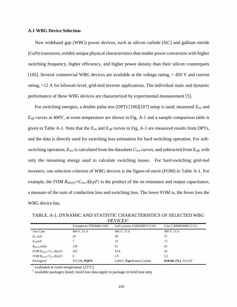
245
A.1 WBG Device Selection
New wideband gap (WBG) power devices, such as silicon carbide (SiC) and gallium nitride
(GaN) transistors, exhibit unique physical characteristics that enable power conversion with higher
switching frequency, higher efficiency, and higher power density than their silicon counterparts
[105]. Several commercial WBG devices are available at the voltage rating, > 450 V and current
rating, >12 A for kilowatt-level, grid-tied inverter applications. The individual static and dynamic
performance of these WBG devices are characterized by experimental measurement [5].
For switching energies, a double pulse test (DPT) [106][107] setup is used; measured Eon and
Eoff curves at 400V, at room temperature are shown in Fig. A-1 and a sample comparison table is
given in Table A-1. Note that the Eon and Eoff curves in Fig. A-1 are measured results from DPTs,
and the data is directly used for switching loss estimation for hard switching operation. For soft-
switching operation, Eoss is calculated from the datasheet Coss curves, and subtracted from Eoff, with
only the remaining energy used to calculate switching losses. For hard-switching grid-tied
inverters, one selection criterion of WBG devices is the figure-of-merit (FOM) in Table A-1. For
example, the FOM Rds(on)×Coss (Ω∙pF) is the product of the on resistance and output capacitance,
a measure of the sum of conduction loss and switching loss. The lower FOM is, the fewer loss the
WBG device has.
TABLE. A-1. DYNAMIC AND STATISTIC CHARACTERISTICS OF SELECTED WBG
DEVICES1 Transphorm TPH3006 [109] GaN systems GS66508P/T [110] Cree C3M0065090J [111]
Test Case: 400 V, 15 A 400 V, 15 A 400 V, 15 A
Eon (μJ) 20 38 37
Eoff (μJ) 7 14 13
Rds(on) (mΩ) 150 55 65
FOM Rds(on)×Ciss (Ω∙pF) 105 10.4 43
FOM Rds(on)×Coss (Ω∙pF) 6 3.5 5.2
Package(s)2 TO-220, PQFN GaNPX, Top/Bottom Cooled D2PAK (7L), TO-247
1 evaluated at room temperature (25°C) 2 available packages listed; listed loss data apply to package in bold font only
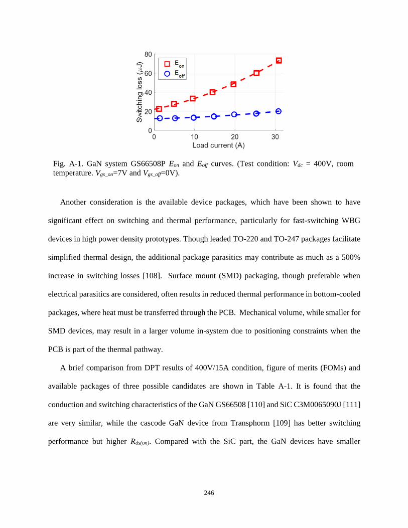
246
Another consideration is the available device packages, which have been shown to have
significant effect on switching and thermal performance, particularly for fast-switching WBG
devices in high power density prototypes. Though leaded TO-220 and TO-247 packages facilitate
simplified thermal design, the additional package parasitics may contribute as much as a 500%
increase in switching losses [108]. Surface mount (SMD) packaging, though preferable when
electrical parasitics are considered, often results in reduced thermal performance in bottom-cooled
packages, where heat must be transferred through the PCB. Mechanical volume, while smaller for
SMD devices, may result in a larger volume in-system due to positioning constraints when the
PCB is part of the thermal pathway.
A brief comparison from DPT results of 400V/15A condition, figure of merits (FOMs) and
available packages of three possible candidates are shown in Table A-1. It is found that the
conduction and switching characteristics of the GaN GS66508 [110] and SiC C3M0065090J [111]
are very similar, while the cascode GaN device from Transphorm [109] has better switching
performance but higher Rds(on). Compared with the SiC part, the GaN devices have smaller
Fig. A-1. GaN system GS66508P Eon and Eoff curves. (Test condition: Vdc = 400V, room
temperature. Vgs_on=7V and Vgs_off=0V).
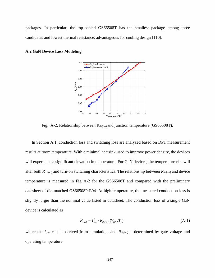
247
packages. In particular, the top-cooled GS66508T has the smallest package among three
candidates and lowest thermal resistance, advantageous for cooling design [110].
A.2 GaN Device Loss Modeling
In Section A.1, conduction loss and switching loss are analyzed based on DPT measurement
results at room temperature. With a minimal heatsink used to improve power density, the devices
will experience a significant elevation in temperature. For GaN devices, the temperature rise will
alter both Rds(on) and turn-on switching characteristics. The relationship between Rds(on) and device
temperature is measured in Fig. A-2 for the GS66508T and compared with the preliminary
datasheet of die-matched GS66508P-E04. At high temperature, the measured conduction loss is
slightly larger than the nominal value listed in datasheet. The conduction loss of a single GaN
device is calculated as
2
( ) ( , )cond rms ds on GS jP I R V T (A-1)
where the Irms can be derived from simulation, and Rds(on) is determined by gate voltage and
operating temperature.
Fig. A-2. Relationship between Rds(on) and junction temperature (GS66508T).
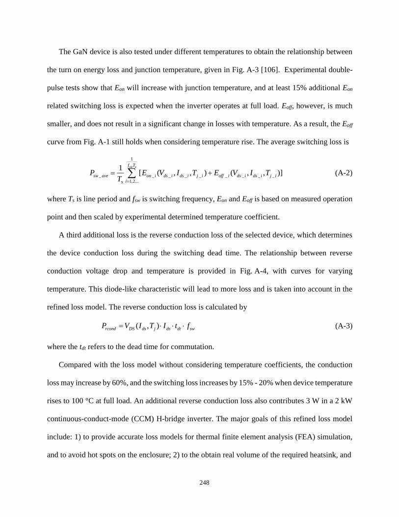
248
The GaN device is also tested under different temperatures to obtain the relationship between
the turn on energy loss and junction temperature, given in Fig. A-3 [106]. Experimental double-
pulse tests show that Eon will increase with junction temperature, and at least 15% additional Eon
related switching loss is expected when the inverter operates at full load. Eoff, however, is much
smaller, and does not result in a significant change in losses with temperature. As a result, the Eoff
curve from Fig. A-1 still holds when considering temperature rise. The average switching loss is
1
_ _ _ _ _ _ _ _ _
1,2...
1[ ( , , ) ( , , )]
sw sf T
sw ave on i ds i ds i j i off i ds i ds i j i
is
P E V I T E V I TT
(A-2)
where Ts is line period and fsw is switching frequency, Eon and Eoff is based on measured operation
point and then scaled by experimental determined temperature coefficient.
A third additional loss is the reverse conduction loss of the selected device, which determines
the device conduction loss during the switching dead time. The relationship between reverse
conduction voltage drop and temperature is provided in Fig. A-4, with curves for varying
temperature. This diode-like characteristic will lead to more loss and is taken into account in the
refined loss model. The reverse conduction loss is calculated by
( , )rcond DS ds j ds dt swP V I T I t f (A-3)
where the tdt refers to the dead time for commutation.
Compared with the loss model without considering temperature coefficients, the conduction
loss may increase by 60%, and the switching loss increases by 15% - 20% when device temperature
rises to 100 °C at full load. An additional reverse conduction loss also contributes 3 W in a 2 kW
continuous-conduct-mode (CCM) H-bridge inverter. The major goals of this refined loss model
include: 1) to provide accurate loss models for thermal finite element analysis (FEA) simulation,
and to avoid hot spots on the enclosure; 2) to the obtain real volume of the required heatsink, and
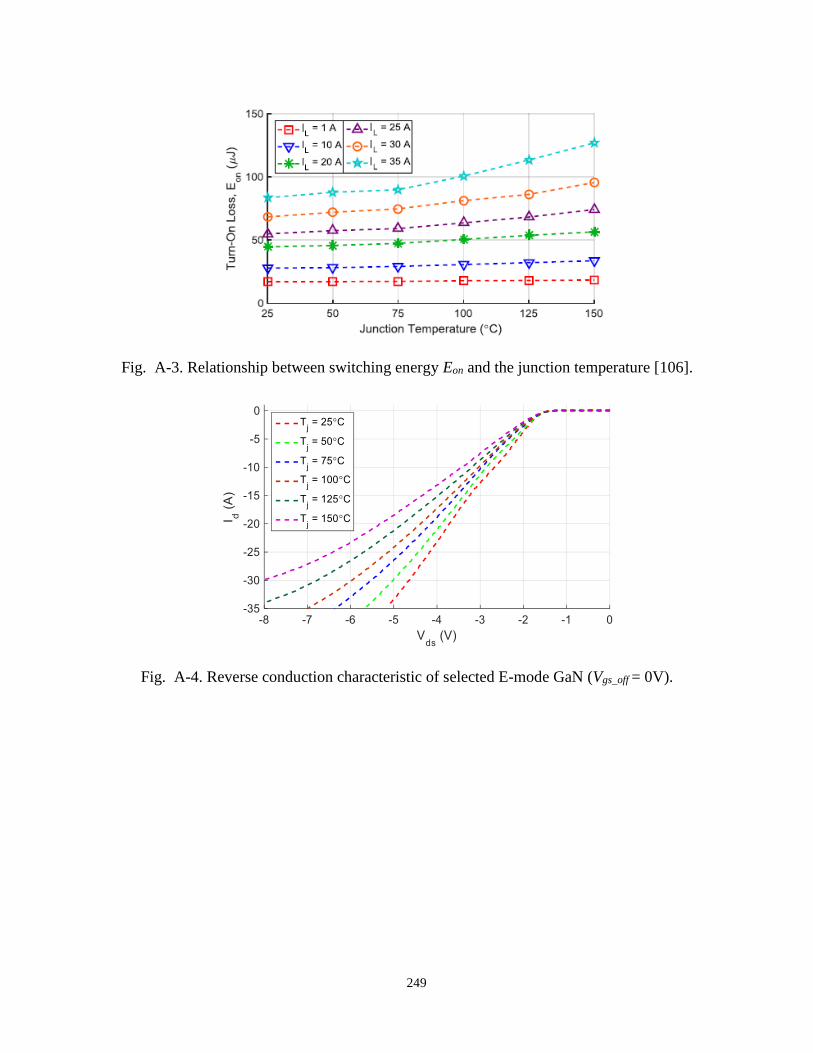
249
Fig. A-3. Relationship between switching energy Eon and the junction temperature [106].
Fig. A-4. Reverse conduction characteristic of selected E-mode GaN (Vgs_off = 0V).

250
to evaluate and select the appropriate switching frequency for CCM operation; 3) to leave enough
design margins to avoid devices operating over their temperature limits.
A.3 Driver Circuit Design and Thermal Implementation
One distinguished feature of WBG devices, compared with Si devices, is high di/dt and dv/dt
resulting from fast switching transitions. The high di/dt may cause overvoltage failures, and driver
misbehavior due to poor common mode transient immunity (CMTI). This effect can be mitigated
to some extent through minimization of driving and power loop inductances, and selection of high
CMTI gate driver. High dv/dt, on the other hand, will induce large currents in parasitic Cgd
capacitances, potentially causing cross-conduction in a phase leg [107]. Generally, this is dealt
with by either slowing down the switching transition, using series resistance between the driver
and the power FET, or by decreasing the gate loop impedance via PCB layout, driver selection, or
additional shunt gate-to-source capacitance. Two passive solutions, additional Cgs and different
turn-on and turn-off gate resistances, are shown in Fig. A-5 and Fig. A-6.
In both gate driver designs, Vgs_on is 7 V and Vgs_off is 0 V, and negative driving voltage is not
adopted for such a power density-oriented application, mainly because extra circuitry generating
negative voltages are required, and more space is needed. Without external anti-parallel diodes,
there will be design trade-offs between increased self-commuted reverse conduction (SCRC)
losses due to negative Vgs_off and increased immunity to false turn-on due to cross-talk during the
switching transition. Several driver configurations were investigated experimentally to confirm the
prototype’s ability to withstand full voltage hard switching without increased losses due to cross-
talk.
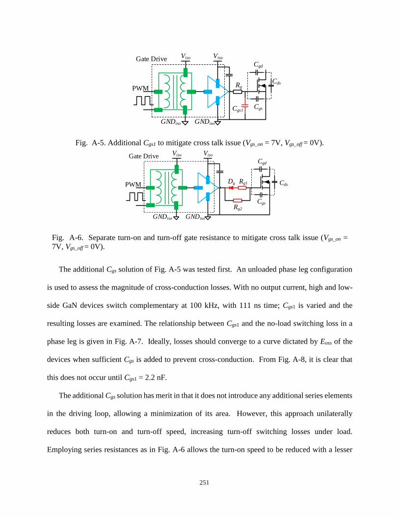
251
The additional Cgs solution of Fig. A-5 was tested first. An unloaded phase leg configuration
is used to assess the magnitude of cross-conduction losses. With no output current, high and low-
side GaN devices switch complementary at 100 kHz, with 111 ns time; Cgs1 is varied and the
resulting losses are examined. The relationship between Cgs1 and the no-load switching loss in a
phase leg is given in Fig. A-7. Ideally, losses should converge to a curve dictated by Eoss of the
devices when sufficient Cgs is added to prevent cross-conduction. From Fig. A-8, it is clear that
this does not occur until Cgs1 = 2.2 nF.
The additional Cgs solution has merit in that it does not introduce any additional series elements
in the driving loop, allowing a minimization of its area. However, this approach unilaterally
reduces both turn-on and turn-off speed, increasing turn-off switching losses under load.
Employing series resistances as in Fig. A-6 allows the turn-on speed to be reduced with a lesser
Fig. A-5. Additional Cgs1 to mitigate cross talk issue (Vgs_on = 7V, Vgs_off = 0V).
Fig. A-6. Separate turn-on and turn-off gate resistance to mitigate cross talk issue (Vgs_on =
7V, Vgs_off = 0V).
PWM
Viso Viso
GNDiso GNDiso
Rg
Cgs1Cgs
Cgd
Cds
Gate Drive
PWM
Viso Viso
GNDiso GNDiso
Rg1
Cgs
Cgd
Cds
Gate Drive
Rg2
Dg

252
impact on turn-off. The no-load switching losses are again assessed with turn-on gate resistance
Rg2 = 10 Ω and turn-off resistance Rg1 = 1 Ω in series with a Schottky diode. The resulting
switching loss curves of two cross-talk mitigation methods are compared in Fig. A-8, showing that
both can achieve similar performance, though the resistive approach may result in lower switching
losses under load if gate loop inductance can still be effectively minimized. In the final prototype,
a configuration of separated turn-on and turn-off driving loops are employed to suppress cross-
talk issue and to reduce switching loss.
Particularly for low capacitance GaN devices, PCB layout also influences the capacitive losses.
Also in Fig. A-8, the difference in losses with the same gate drive configuration for two different
PCB layouts is shown. When a large ground plane is present underneath the device, extra parasitic
layout capacitance leads to additional switching loss. In subsequent revisions of the prototype, the
ground plane under the devices is eliminated, and the different turn-on/off gate resistance method
is employed.
One key criterion to select a gate driver IC for GaN devices is the high common mode transient
immunity. During the period of prototype design, two candidates, which are ADUM7223 using
monolithic transformer-based magnetic isolation [112], and Si823X with radio frequency carrier-
based isolation [113], were commercially available. Unfortunately, neither gate driver ICs can
meet a CMTI > 150V/ns, based on experimental test results. Still, the gate driver IC, ADUM7223,
was adopted in the final prototype, and no CMTI caused failure occurred during benchtop tests. A
latest gate driver IC, Si827X, which achieves a CMTI > 200V/ns, is available since beginning of
2016 [114]. This new gate driver, compared with aforementioned ones, is more suitable for WBG
applications with its higher CMTI.
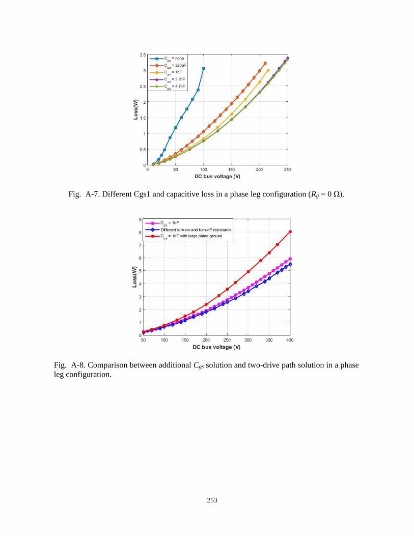
253
Fig. A-7. Different Cgs1 and capacitive loss in a phase leg configuration (Rg = 0 Ω).
Fig. A-8. Comparison between additional Cgs solution and two-drive path solution in a phase
leg configuration.
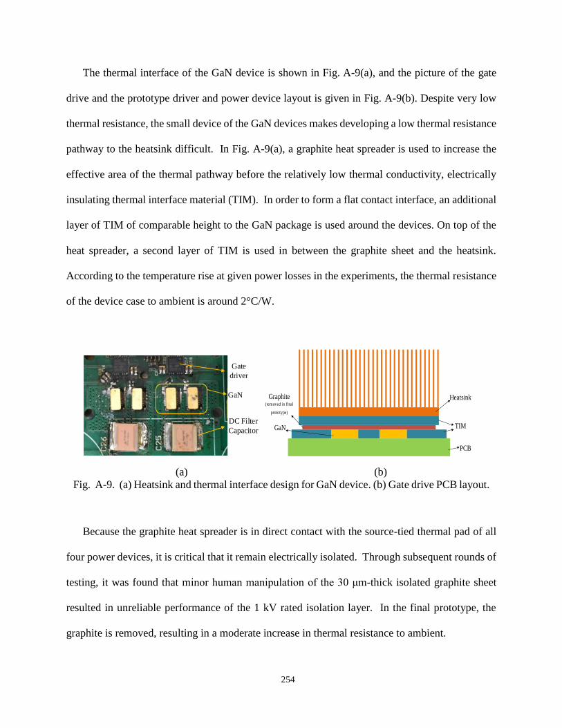
254
The thermal interface of the GaN device is shown in Fig. A-9(a), and the picture of the gate
drive and the prototype driver and power device layout is given in Fig. A-9(b). Despite very low
thermal resistance, the small device of the GaN devices makes developing a low thermal resistance
pathway to the heatsink difficult. In Fig. A-9(a), a graphite heat spreader is used to increase the
effective area of the thermal pathway before the relatively low thermal conductivity, electrically
insulating thermal interface material (TIM). In order to form a flat contact interface, an additional
layer of TIM of comparable height to the GaN package is used around the devices. On top of the
heat spreader, a second layer of TIM is used in between the graphite sheet and the heatsink.
According to the temperature rise at given power losses in the experiments, the thermal resistance
of the device case to ambient is around 2°C/W.
Because the graphite heat spreader is in direct contact with the source-tied thermal pad of all
four power devices, it is critical that it remain electrically isolated. Through subsequent rounds of
testing, it was found that minor human manipulation of the 30 μm-thick isolated graphite sheet
resulted in unreliable performance of the 1 kV rated isolation layer. In the final prototype, the
graphite is removed, resulting in a moderate increase in thermal resistance to ambient.
Heatsink
TIM
PCB
Graphite(removed in final
prototype)
GaN
(a) (b)
Fig. A-9. (a) Heatsink and thermal interface design for GaN device. (b) Gate drive PCB layout.
Gate
driver
GaN
DC Filter
Capacitor
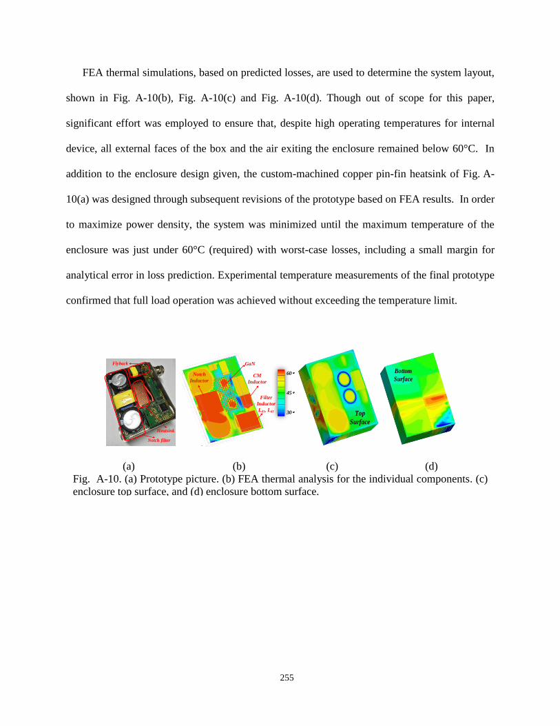
255
FEA thermal simulations, based on predicted losses, are used to determine the system layout,
shown in Fig. A-10(b), Fig. A-10(c) and Fig. A-10(d). Though out of scope for this paper,
significant effort was employed to ensure that, despite high operating temperatures for internal
device, all external faces of the box and the air exiting the enclosure remained below 60°C. In
addition to the enclosure design given, the custom-machined copper pin-fin heatsink of Fig. A-
10(a) was designed through subsequent revisions of the prototype based on FEA results. In order
to maximize power density, the system was minimized until the maximum temperature of the
enclosure was just under 60°C (required) with worst-case losses, including a small margin for
analytical error in loss prediction. Experimental temperature measurements of the final prototype
confirmed that full load operation was achieved without exceeding the temperature limit.
Notch
Inductor
Filter
Inductor
Ld1, Ld2
CM
Inductor
GaN
60
45
30
(a) (b) (c) (d)
Fig. A-10. (a) Prototype picture. (b) FEA thermal analysis for the individual components. (c)
enclosure top surface, and (d) enclosure bottom surface.
Notch filter
Heatsink
Flyback
Top
Surface
Bottom
Surface
256
Vita
Chongwen Zhao (S’13) received the B.Sc. degree from the School of Electronic Engineering,
Xidian University, Xi’an, China, in 2011, and received the M.Sc. degree from the College of
Electrical Engineering, Zhejiang University, Hangzhou, China, in 2014. Currently, he is working
toward the Ph.D. degree in electrical engineering at the University of Tennessee, Knoxville, TN,
USA.
His research interests include wireless power and communication applications, high power
density and high frequency converter design using wide bandgap devices.
Related Documents