Multi-channel Digital Receiver Data Acquisition System for the Arecibo Radar A thesis submitted to the Graduate School University of Arkansas at Little Rock in partial fulfillment for requirements for the degree of MASTER OF SCIENCE in Applied Science in the Department of Applied Science of the Donaghey Systems Engineering and Science August 2006 Ryan Seal B.S., University of Arkansas at Little Rock, 2001

Welcome message from author
This document is posted to help you gain knowledge. Please leave a comment to let me know what you think about it! Share it to your friends and learn new things together.
Transcript
Multi-channel Digital Receiver Data Acquisition System for the AreciboRadar
A thesis submittedto the Graduate School
University of Arkansas at Little Rock
in partial fulfillment for requirementsfor the degree of
MASTER OF SCIENCE
in Applied Science
in the Department of Applied Scienceof the Donaghey Systems Engineering and Science
August 2006
Ryan Seal
B.S., University of Arkansas at Little Rock, 2001

c©Copyright 2006 Ryan SealAll Rights Reserved
1
This thesis, “Multi-channel Digital Receiver Data Acquisition System for the AreciboRadar”, by Ryan Seal, is approved by:
Thesis Advisor
Dr. Urbina, JulioProfessor of ECET
Thesis Committee
Dr. Al-Rizzo, HussainProfessor of Systems Engineering
Dr. Milanova, MariofannaProfessor of Computer Science
Dr. Mohan, SeshadriChair of Systems Engineering
Program Coordinator
Dr. Al-Shukri, HaydarApplied Science
Graduate Dean
2

In presenting this thesis in partial fulfillment of requirements for a Master’s degreeat the University of Arkansas at Little Rock, I agree that the library should make copiesfreely available for inspection. I further agree that extensive copying of this thesis isallowable only for scholarly purposes, consistent with “fair use” as prescribed in the U.S.Copyright Law. Any reproduction for any purpose or by any means shall not be allowedwithout my written consent.
Signature
Date
3
Contents
Abstract ii
Acknowledgments iii
List of Figures vi
List of Tables vi
List of Abbreviations viii
1 Introduction 1
1.1 Radar Techniques . . . . . . . . . . . . . . . . . . . . . . . . . . . . . . . 2
1.2 Radar Receivers . . . . . . . . . . . . . . . . . . . . . . . . . . . . . . . . 4
1.3 Digital Signal Processing . . . . . . . . . . . . . . . . . . . . . . . . . . . 8
1.3.1 Analog-to-Digital Conversion . . . . . . . . . . . . . . . . . . . . 8
1.3.2 Discrete Time Systems . . . . . . . . . . . . . . . . . . . . . . . . 14
1.3.3 Multirate Systems . . . . . . . . . . . . . . . . . . . . . . . . . . 17
1.4 Software Analysis and Design . . . . . . . . . . . . . . . . . . . . . . . . 22
1.4.1 Object Oriented Programming . . . . . . . . . . . . . . . . . . . . 22
1.4.2 Unified Modeling Language . . . . . . . . . . . . . . . . . . . . . 23
4
2 System Analysis and Design 25
2.1 Requirements Analysis . . . . . . . . . . . . . . . . . . . . . . . . . . . . 26
2.2 System Configuration . . . . . . . . . . . . . . . . . . . . . . . . . . . . . 29
2.2.1 Configuration Graphical Interface . . . . . . . . . . . . . . . . . . 43
2.3 Data Acquisition . . . . . . . . . . . . . . . . . . . . . . . . . . . . . . . 45
2.3.1 Hardware / Software Interface . . . . . . . . . . . . . . . . . . . . 45
2.4 Real-Time Data Display . . . . . . . . . . . . . . . . . . . . . . . . . . . 52
2.5 Data Format and Storage . . . . . . . . . . . . . . . . . . . . . . . . . . 52
2.5.1 Data Header Format . . . . . . . . . . . . . . . . . . . . . . . . . 58
3 Radar Observations 60
3.1 Meteor Observations . . . . . . . . . . . . . . . . . . . . . . . . . . . . . 60
3.1.1 Detection Algorithm . . . . . . . . . . . . . . . . . . . . . . . . . 61
3.1.2 Parameter Estimation . . . . . . . . . . . . . . . . . . . . . . . . 62
3.2 Plasma Line Observations . . . . . . . . . . . . . . . . . . . . . . . . . . 67
4 Conclusions and Future Work 69
Appendix 69
A Convolution Sum Derivation . . . . . . . . . . . . . . . . . . . . . . . . . I
B MATLAB Programs . . . . . . . . . . . . . . . . . . . . . . . . . . . . . II
B.1 metFreq.m . . . . . . . . . . . . . . . . . . . . . . . . . . . . . . . II
i
Abstract
Digital Receivers are commercially available, cost effective solutions that are becoming
commonplace in modern data acquisition systems (DAS). The digital receiver has the
ability to be reconfigured via software, making modern DAS flexible for a variety of
applications. This thesis describes the design and implementation of a complete data
acquisition system using a general purpose computer (GPC) equipped with a digital
receiver card. This system will replace the older DAS (baseband sampling) used by the
Space and Atmospheric Science (SAS) group at the Arecibo Observatory (AO). Emphasis
is placed on a generic system easily adaptable to a specific application with minimal
effort. A full discussion of the system will be given with concentration on the receiver’s
capabilities and software design. Algorithms and design strategy are discussed to properly
document optimizations and features required by the system. Finally, we present two
radar observations with this system and illustrate results.
ii

Acknowledgments
Writing a thesis has proven more of a challenge than I ever imagined. Much time has
passed and many people have been involved along the way. First and foremost, I would
like to thank my thesis advisor Prof. Julio Urbina for providing the opportunity, support,
and his persistent personality which has helped complete this work. I also thank Jocelyn,
family, and friends for putting up with my sometimes less than joyous moods. The
entire staff at the Arecibo Observatory deserve thanks with special thanks to Dr. Sixto
Gonzalez, Dr. Mike Sulzer, and Dr. Nestor Aponte for valuable insight, advice, and a
few good laughs. Thanks to Jeff Hagen for assistance in the development of the device
driver. Thanks to Dr. Diego Janches for his help with meteor analysis. Thanks to
Prof. Farzad Kamalabadi and those involved from the University of Illinios at Urbana-
Champaign for equipment and support. Thanks to Prof. Hirak Patangia for providing
motivation, direction, and interest in the subject of engineering. Lastly, I would like to
thank my thesis committee for their time. Of course, there are probably many others I
have forgotten about, so I now take the time to thank these individuals whose names fail
me now but will probably resurface after submission.
iii
List of Figures
1.1 Backscatter Radar Layout . . . . . . . . . . . . . . . . . . . . . . . . . . 3
1.2 Range Time Diagram . . . . . . . . . . . . . . . . . . . . . . . . . . . . . 3
1.3 Signal Mixer . . . . . . . . . . . . . . . . . . . . . . . . . . . . . . . . . . 5
1.4 Superheterodyne Analog Receiver with Quadrature mixing . . . . . . . . 6
1.5 Superheterodyne Digital Receiver with Quadrature mixers . . . . . . . . 6
1.6 Numerically Controlled Oscillator . . . . . . . . . . . . . . . . . . . . . . 7
1.7 N-bit Digital Phase Wheel . . . . . . . . . . . . . . . . . . . . . . . . . . 7
1.8 Digital Sampling . . . . . . . . . . . . . . . . . . . . . . . . . . . . . . . 10
1.9 2 level quantization . . . . . . . . . . . . . . . . . . . . . . . . . . . . . . 11
1.10 noise probability distribution . . . . . . . . . . . . . . . . . . . . . . . . . 12
1.11 quantization error model . . . . . . . . . . . . . . . . . . . . . . . . . . . 13
1.12 3-bit two’s complement integer representation . . . . . . . . . . . . . . . 14
1.13 Discrete Time System . . . . . . . . . . . . . . . . . . . . . . . . . . . . 15
1.14 Basic System Operations . . . . . . . . . . . . . . . . . . . . . . . . . . . 15
1.15 Image bandwidth . . . . . . . . . . . . . . . . . . . . . . . . . . . . . . . 17
1.16 Decimation Image Filter . . . . . . . . . . . . . . . . . . . . . . . . . . . 17
1.17 Resulting spectrum from decimation . . . . . . . . . . . . . . . . . . . . 18
1.18 Decimation Block Diagram . . . . . . . . . . . . . . . . . . . . . . . . . . 18
iv

1.19 Quantization noise power . . . . . . . . . . . . . . . . . . . . . . . . . . . 19
1.20 Sampled images . . . . . . . . . . . . . . . . . . . . . . . . . . . . . . . . 20
1.21 Interpolation Image Filter . . . . . . . . . . . . . . . . . . . . . . . . . . 21
1.22 Resulting spectrum after interpolation . . . . . . . . . . . . . . . . . . . 21
1.23 Interpolation Block Diagram . . . . . . . . . . . . . . . . . . . . . . . . . 21
2.1 Use Case Analysis . . . . . . . . . . . . . . . . . . . . . . . . . . . . . . . 27
2.2 Echotek-GC214PCI Diagram . . . . . . . . . . . . . . . . . . . . . . . . 28
2.3 GC214 Class Diagram . . . . . . . . . . . . . . . . . . . . . . . . . . . . 29
2.4 GC4016 Channel . . . . . . . . . . . . . . . . . . . . . . . . . . . . . . . 31
2.5 IOBlock Interface and IOChannel Class Diagrams . . . . . . . . . . . . . 31
2.6 ZeroPad Diagrams . . . . . . . . . . . . . . . . . . . . . . . . . . . . . . 33
2.7 Single Stage Discrete Integrator . . . . . . . . . . . . . . . . . . . . . . . 35
2.8 Single Stage Discrete Differentiator . . . . . . . . . . . . . . . . . . . . . 35
2.9 MultiStage Decimating CIC Filter . . . . . . . . . . . . . . . . . . . . . . 36
2.10 CIC Diagrams . . . . . . . . . . . . . . . . . . . . . . . . . . . . . . . . . 37
2.11 Coarse Gain Diagrams . . . . . . . . . . . . . . . . . . . . . . . . . . . . 39
2.12 FIR Diagrams . . . . . . . . . . . . . . . . . . . . . . . . . . . . . . . . . 39
2.13 CFIR Diagrams . . . . . . . . . . . . . . . . . . . . . . . . . . . . . . . . 40
2.14 PFIR Diagrams . . . . . . . . . . . . . . . . . . . . . . . . . . . . . . . . 40
2.15 Fine Gain Diagrams . . . . . . . . . . . . . . . . . . . . . . . . . . . . . 41
2.16 Resampler Diagrams . . . . . . . . . . . . . . . . . . . . . . . . . . . . . 42
2.17 Main Configuration Window . . . . . . . . . . . . . . . . . . . . . . . . . 43
2.18 Channel Configuration Window . . . . . . . . . . . . . . . . . . . . . . . 44
2.19 PLX9080 DMA Descriptor Layout . . . . . . . . . . . . . . . . . . . . . . 46
v
2.20 Echotek-GC214 FIFO Layout . . . . . . . . . . . . . . . . . . . . . . . . 46
2.21 Memory Buffer Layout . . . . . . . . . . . . . . . . . . . . . . . . . . . . 48
2.22 Producer Consumer Activity Diagram . . . . . . . . . . . . . . . . . . . 49
2.23 Consumer Activity Diagram . . . . . . . . . . . . . . . . . . . . . . . . . 50
2.24 Producer Activity Diagram . . . . . . . . . . . . . . . . . . . . . . . . . 50
2.25 Run Time GUI . . . . . . . . . . . . . . . . . . . . . . . . . . . . . . . . 51
2.26 SHS Layout . . . . . . . . . . . . . . . . . . . . . . . . . . . . . . . . . . 55
2.27 SHS File ID . . . . . . . . . . . . . . . . . . . . . . . . . . . . . . . . . . 55
2.28 Keyword format . . . . . . . . . . . . . . . . . . . . . . . . . . . . . . . . 55
2.29 Keyword format . . . . . . . . . . . . . . . . . . . . . . . . . . . . . . . . 56
3.1 Range Time Intensity (RTI) plot . . . . . . . . . . . . . . . . . . . . . . 63
3.2 IPP illustrating meteor in time domain . . . . . . . . . . . . . . . . . . . 64
3.3 IPP power computation . . . . . . . . . . . . . . . . . . . . . . . . . . . 65
3.4 IPP cross-correlation with transmitted power to isolate detection . . . . . 65
3.5 Isolated Meteor detection resulting from cross-correlation . . . . . . . . . 66
3.6 Spectrum from meteor detection illustrating doppler spectrum . . . . . . 66
vi
List of Abbreviations
1. ADC Analog to Digital Converter
2. AO Arecibo Observatory
3. ASIC Application Specific Integrated Cicuit
4. CIC Cascaded Integrator Comb Filter
5. COTS Commercial off-the-shelf
6. DAS Data Acquisition System
7. DDC Digital DownConverter
8. DFT Discrete Fourier Transform
9. DNL Differential Non-Linearity
10. DSP Digital Signal Processing
11. FFT Fast Fourier Transform
12. FIR Finite Impulse Response
13. GPC General Purpose Computer
vii

14. IC Integrated Circuit
15. IF Intermediate Frequency
16. IIR Infinite Impulse Response
17. INL Integral Non-Linearity
18. IPP Inter-Pulse Period
19. LSB Least Significant Bit
20. LTI Linear Time Invariant Systems
21. NCO Numerically Controlled Oscillator
22. OOD Object Oriented Design
23. OOP Object Oriented Programming
24. OSR OverSampling Ratio
25. SDR Software Defined Radio
26. UML Unified Modeling Language
viii
Chapter 1
Introduction
Motivation for this work is to explore the use of commercial off-the-shelf (COTS) dig-
ital receivers, commonly used in Software Defined Radio (SDR) architectures, for use
in modern data aquisition systems (DAS); and, in this specific application, space and
atmospheric research at the Arecibo Observatory (AO). In the past, traditional receiver
architectures implemented a superheterodyne architecture combined with digitization
at baseband. In contrast, modern digital receiver architectures sample at intermediate
frequencies (IF). This key difference reduces the receiver architecture’s complexity and
lessens analog component specifications while removing gain and phase imbalances found
in analog quadrature mixers. Advances in semiconductor technology are slowly moving
the receiver’s digitization point closer to the receiver’s front-end. Currently, digital re-
ceivers are capable of digitizing data at intermediate frequencies (IF) and, depending on
the system, RF sampling is a possibility. Modern DAS [23, 14], the focus of this thesis,
encompass both back-end digital receivers and general purpose computers (GPC). The
combination of both digital receiver and GPC form the basis of a modern DAS which
typically perform three tasks: 1) digitization, or sampling of analog signal(s), 2) digital
1
signal processing (DSP), 3) formatting and storage of data. The remainder of this chapter
will provide an overview of techniques related to radar operation, signal processing, and
software design required for the discussion of modern DAS; which is the central topic of
this thesis. In Chapter 2, an in-depth study of the system’s internals, including the digital
receiver hardware and software is presented. Chapter 3 will illustrate data from multiple
radar observations. Finally, conclusions and future work are discussed in Chapter 4.
1.1 Radar Techniques
Backscatter radars operate in both transmit and receive modes by isolating each mode us-
ing mechanical (duplexer) or electrical (T/R switch) devices as shown in Figure 1.1.These
type of radars transmit short, periodic waveforms p(t) with a duty cycle
δ(t)
T, (1.1)
where δ(t) is the transmitter pulse width and T is the period; (1.1) is also called the
interpulse period (IPP). The complete transmitted signal of the radar
s(t) = p(t)ejω0t (1.2)
is a combination of the modulating waveform p(t) and a carrier frequency eω0t. In receive
mode, backscatter radar returns are sampled by the radar receiver for further analysis.
The sampled signal αs(t − 2r/c) is returned from a radar target at range r as depicted
in Figure 1.2.
Ionospheric plasma-density irregularities are typically observed with pulsed backscat-
ter radars that operate at twice the wavelength of ionospheric density fluctuations. Only
2
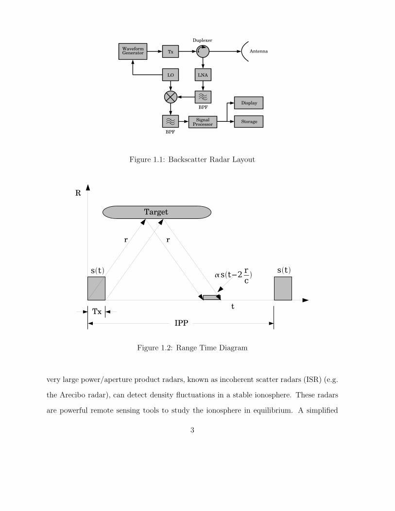
Figure 1.1: Backscatter Radar Layout
Figure 1.2: Range Time Diagram
very large power/aperture product radars, known as incoherent scatter radars (ISR) (e.g.
the Arecibo radar), can detect density fluctuations in a stable ionosphere. These radars
are powerful remote sensing tools to study the ionosphere in equilibrium. A simplified
3
model of the average received power (< Pr >) in an ISR experiment is described by
< Pr >= ηPt
AmaxδR
4πR2σN, (1.3)
where η is the system calibration factor (that takes into account ohmic losses, etc), Pt is
transmitted power, σ is backscatter radar cross section of a free electron, N is the average
electron density, R is the radar range, Amax is the effective area of the radar antenna,
and δR is the range resolution [10].
1.2 Radar Receivers
In general, a radar receiver performs the following tasks: 1) detect and isolate a desired
signal in the presence of noise, 2) translate the signal into a format compatible with the
system, and 3) digitize the signal for further processing.
In radar systems, the antenna is sensitive to the desired RF signals and largely de-
termines the signal-to-noise ratio (SNR) of the detected signal. After detection, filtering
and amplification isolate the desired signal from unwanted noise and the signal’s spectral
content is down-shifted to alleviate physical limitations in the processing chain. Combi-
nation of these processes define a receiver’s topology and many topologies exist [14, 23],
with each providing unique characterisitics. Of these, the superheterodyne architecture
is commonly used due to many advantages including: 1) amplifier and filter requirements
are lessened, 2) decoupling of the front- and back- ends, and 3) components are widely
available for standard intermediate frequencies (IF). This architecture uses one or more
stages of down-conversion to shift the signal down to a specified IF. In the analog domain,
4

the down-conversion process is a multiplication of two signals
y(t) = sLO(t)sm(t), where
sLO(t) = e−jωLOt
sm(t) = Am(t)ejωLOt+θm(t).
A graphical representation is shown in Figure 1.3. Combination of the superheterodyne
Figure 1.3: Signal Mixer
architecture and analog quadrature mixing for baseband conversion are key features of a
traditional radar receiver. In this configuration, quadrature down-conversion translates
the IF signal to baseband while preserving both amplitude and phase, which are required
for coherent sampling. An overview of the traditional radar architecture is illustrated in
Figure 1.4.
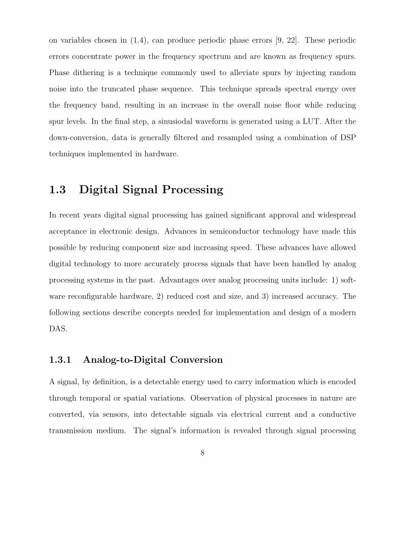
A modern form of radar receiver samples the IF signal allowing quadrature down-
conversion in the digital domain; these receivers are labeled digital receivers and the
general topology is depicted in Figure 1.5. Sampling IF signals enable systems to employ
a technique known as bandpass sampling [24] in addition to nyquist sampling used in
traditional receivers. The primary difference between the digital and traditional archi-
tectures is the position of the down-converting mixers; consequently, this detail defines
the two architectures. The digital receiver digitally down-converts an IF signal using a
Digital Down-Converter (DDC). The DDC [1] provides superior performance to conven-
5
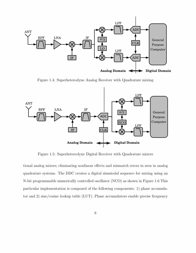
Figure 1.4: Superheterodyne Analog Receiver with Quadrature mixing
Figure 1.5: Superheterodyne Digital Receiver with Quadrature mixers
tional analog mixers; eliminating nonlinear effects and mismatch errors in seen in analog
quadrature systems. The DDC creates a digital sinusiodal sequence for mixing using an
N-bit programmable numerically controlled oscillator (NCO) as shown in Figure 1.6 This
particular implementation is composed of the following components: 1) phase accumula-
tor and 2) sine/cosine lookup table (LUT). Phase accumulators enable precise frequency
6

Figure 1.6: Numerically Controlled Oscillator
tuning, typically with sub-hertz resolution. Accumulation of phase, via feedback, is best
described using a digital phase wheel as shown in Figure 1.7. The phase wheel contains
Figure 1.7: N-bit Digital Phase Wheel
a vector rotating counter-clockwise (CCW) at a rate fout determined by
fout = fclk
M
2N, (1.4)
where M is the tuning word, N is the bit resolution, and fclk is the input clock rate.
As the vector rotates, a linear sum is produced at the output. A static phase offset
is programmed using a P − bit phase word. In order to reduce storage requirements,
bit reduction, or phase truncation is needed. For example, a 32-bit accumulator would
require a minimum storage of 230 entries; and, when combined with the precision of
the entry, total storage could exceed 1 GB. Notice that phase truncation, depending
7
on variables chosen in (1.4), can produce periodic phase errors [9, 22]. These periodic
errors concentrate power in the frequency spectrum and are known as frequency spurs.
Phase dithering is a technique commonly used to alleviate spurs by injecting random
noise into the truncated phase sequence. This technique spreads spectral energy over
the frequency band, resulting in an increase in the overall noise floor while reducing
spur levels. In the final step, a sinusiodal waveform is generated using a LUT. After the
down-conversion, data is generally filtered and resampled using a combination of DSP
techniques implemented in hardware.
1.3 Digital Signal Processing
In recent years digital signal processing has gained significant approval and widespread
acceptance in electronic design. Advances in semiconductor technology have made this
possible by reducing component size and increasing speed. These advances have allowed
digital technology to more accurately process signals that have been handled by analog
processing systems in the past. Advantages over analog processing units include: 1) soft-
ware reconfigurable hardware, 2) reduced cost and size, and 3) increased accuracy. The
following sections describe concepts needed for implementation and design of a modern
DAS.
1.3.1 Analog-to-Digital Conversion
A signal, by definition, is a detectable energy used to carry information which is encoded
through temporal or spatial variations. Observation of physical processes in nature are
converted, via sensors, into detectable signals via electrical current and a conductive
transmission medium. The signal’s information is revealed through signal processing
8
techniques. Since the advent of digital computers, signal processing and data storage
techniques typically operate in the digital domain; drastically improving performance
while decreasing storage requirements. Digital sampling is a process of transforming a
continuous signal into a discrete sequence; this process is achieved through an analog-to-
digital converter (ADC) chip. The operation performed by the ADC can be viewed as
a process consisting of three steps: 1) sampling, 2) quantization, and 3) encoding of the
signal. The first step of the conversion - sampling, performs the continuous to discrete
conversion. For example, a pure analog sinusoid is described by
sa(t) = A sin(2πFt + φ) ≡ A sin(Ωt + φ), (1.5)
where the sub-notation a denotes an analog signal, A is the amplitude, F is frequency in
hertz (Hz), Ω is angular velocity in radians per second (rad/s), and φ is the phase con-
stant. Discussion is limited to uniform sampling which are samples taken at equidistant
points with respect to time. The number of samples required to adequately represent a
continuous waveform is given by Nyquist’s theorem [20]
Fs ≥ 2B, (1.6)
where Fs is the sampling rate and B is the signal’s bandwidth. A discrete version of (1.5)
is given by
sa(nT ) = A sin(ΩnT + φn), (1.7)
where n is the sample number and T is the sample period. Both forms are illustrated
in Figure 1.8. The sample period is inversely related to the sample frequency Fs = 1/T
with units of samples per second (SPS). The ratio of continuous frequency to sampled
9
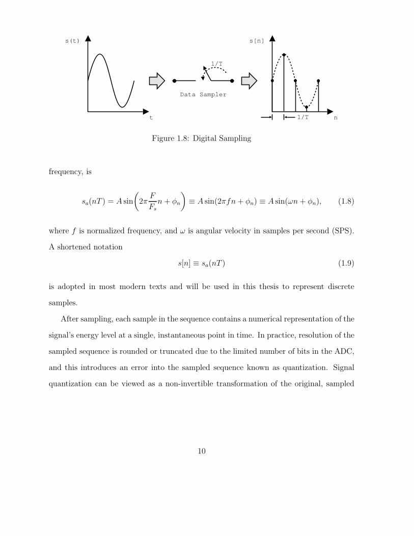
s(t)
t
s[n]
n
Data Sampler
1/T
1/T
Figure 1.8: Digital Sampling
frequency, is
sa(nT ) = A sin
(
2πF
Fs
n + φn
)
≡ A sin(2πfn + φn) ≡ A sin(ωn + φn), (1.8)
where f is normalized frequency, and ω is angular velocity in samples per second (SPS).
A shortened notation
s[n] ≡ sa(nT ) (1.9)
is adopted in most modern texts and will be used in this thesis to represent discrete
samples.
After sampling, each sample in the sequence contains a numerical representation of the
signal’s energy level at a single, instantaneous point in time. In practice, resolution of the
sampled sequence is rounded or truncated due to the limited number of bits in the ADC,
and this introduces an error into the sampled sequence known as quantization. Signal
quantization can be viewed as a non-invertible transformation of the original, sampled
10
sequence. Quantization is described by
xq[n] = Q
[
x[n]
]
, (1.10)
and the resulting error is
eq[n] = xq[n] − x[n]. (1.11)
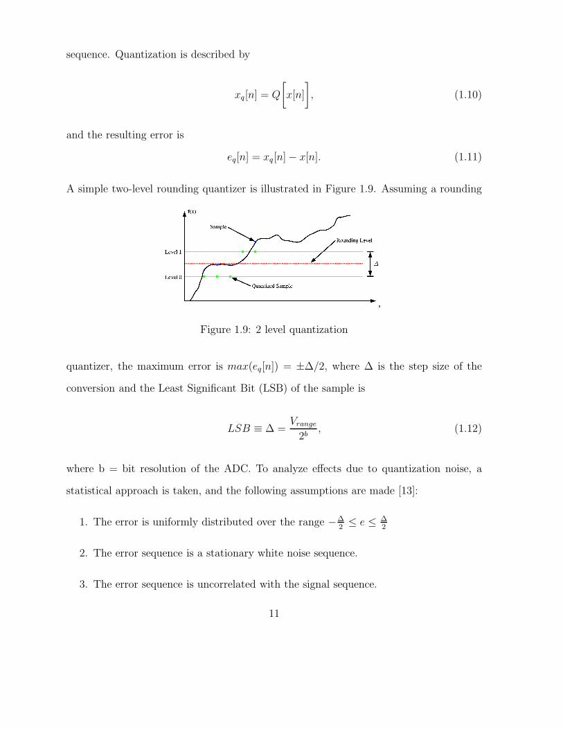
A simple two-level rounding quantizer is illustrated in Figure 1.9. Assuming a rounding
Figure 1.9: 2 level quantization
quantizer, the maximum error is max(eq[n]) = ±∆/2, where ∆ is the step size of the
conversion and the Least Significant Bit (LSB) of the sample is
LSB ≡ ∆ =Vrange
2b, (1.12)
where b = bit resolution of the ADC. To analyze effects due to quantization noise, a
statistical approach is taken, and the following assumptions are made [13]:
1. The error is uniformly distributed over the range −∆2≤ e ≤ ∆
2
2. The error sequence is a stationary white noise sequence.
3. The error sequence is uncorrelated with the signal sequence.
11
4. The signal sequence is zero mean and stationary.
The probability density function (pdf) of the error signal is defined as
p(e) =
1∆
−∆2≤ e ≤ ∆
2
0 elsewhere
(1.13)
and an illustration is provided in Figure 1.10 The mean-square noise power is
Figure 1.10: noise probability distribution
Pn ≡ σ2e =
∫ ∆
2
−∆
2
e2p(e)de =1
∆
∫ ∆
2
−∆
2
e2de =∆2
12. (1.14)
The Signal to Quantization Noise Ratio (SQNR) provides a comparison of signal power
vs. noise power due to quantization
SQNR = 10 log
(
Px
Pn
)
= 20log
(
σx
σe
)
; (1.15)
this equation reduces to
SQNR = 10.79 + 6.02b + 10 log(FFS), (1.16)
12
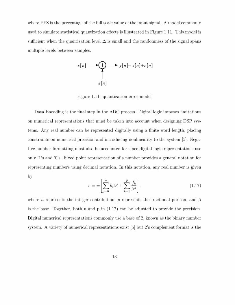
where FFS is the percentage of the full scale value of the input signal. A model commonly
used to simulate statistical quantization effects is illustrated in Figure 1.11. This model is
sufficient when the quantization level ∆ is small and the randomness of the signal spans
multiple levels between samples.
Figure 1.11: quantization error model
Data Encoding is the final step in the ADC process. Digital logic imposes limitations
on numerical representations that must be taken into account when designing DSP sys-
tems. Any real number can be represented digitally using a finite word length, placing
constraints on numerical precision and introducing nonlinearity to the system [5]. Nega-
tive number formatting must also be accounted for since digital logic representations use
only ’1’s and ’0’s. Fixed point representation of a number provides a general notation for
representing numbers using decimal notation. In this notation, any real number is given
by
r = ±[
n∑
j=0
bjβj +
p∑
k=1
fk
βk
]
, (1.17)
where n represents the integer contribution, p represents the fractional portion, and β
is the base. Together, both n and p in (1.17) can be adjusted to provide the precision.
Digital numerical representations commonly use a base of 2, known as the binary number
system. A variety of numerical representations exist [5] but 2’s complement format is the
13
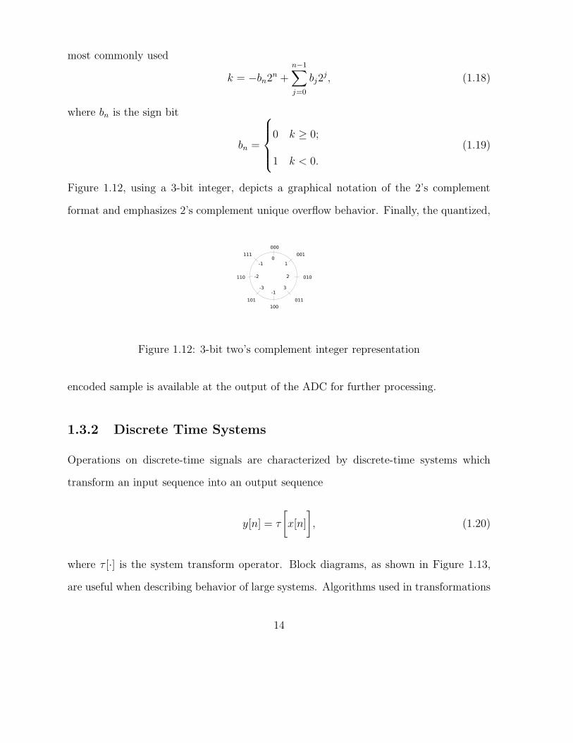
most commonly used
k = −bn2n +
n−1∑
j=0
bj2j, (1.18)
where bn is the sign bit
bn =
0 k ≥ 0;
1 k < 0.
(1.19)
Figure 1.12, using a 3-bit integer, depicts a graphical notation of the 2’s complement
format and emphasizes 2’s complement unique overflow behavior. Finally, the quantized,
Figure 1.12: 3-bit two’s complement integer representation
encoded sample is available at the output of the ADC for further processing.
1.3.2 Discrete Time Systems
Operations on discrete-time signals are characterized by discrete-time systems which
transform an input sequence into an output sequence
y[n] = τ
[
x[n]
]
, (1.20)
where τ [·] is the system transform operator. Block diagrams, as shown in Figure 1.13,
are useful when describing behavior of large systems. Algorithms used in transformations
14
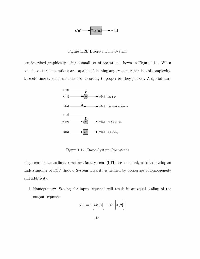
Figure 1.13: Discrete Time System
are described graphically using a small set of operations shown in Figure 1.14. When
combined, these operations are capable of defining any system, regardless of complexity.
Discrete-time systems are classified according to properties they possess. A special class
Figure 1.14: Basic System Operations
of systems known as linear time-invariant systems (LTI) are commonly used to develop an
understanding of DSP theory. System linearity is defined by properties of homogeneity
and additivity.
1. Homogeneity: Scaling the input sequence will result in an equal scaling of the
output sequence.
y[t] ≡ τ
[
kx[n]
]
= kτ
[
x[n]
]
15
2. Additivity: An output response due to a summation of input sequences is equivalent
to a sum of the output response of each individual input sequence.
y[t] ≡ τ
[
x1[t] + x2[t]
]
= τ
[
x1[t]
]
+ τ
[
x2[t]
]
Time-invariance is used to describe a system with no dependence on time and is expressed
by
y[n − k] = τ
[
x[n − k]
]
. (1.21)
Comination of these two principles define the LTI system and thi system is completely
defined by its impulse response in an operation known as the convolution sum A
y[n] =
k=∞∑
k=0
h[k]x[n − k]. (1.22)
Systems employing digital filtering techniques make use of (1.22) and two types of
digital filters exist:
1. Finite Impulse Response (FIR) Filter: This filter provides stability and linear phase
response due to its finite response h[n].
2. Infinite Impulse Response (IIR) Filter: These filters are used due to their efficient,
recursive structure.
Of the two filter types, focus is given to FIR filters and interested readers are directed to
[15, 17, 18, 13] for further reading.
16
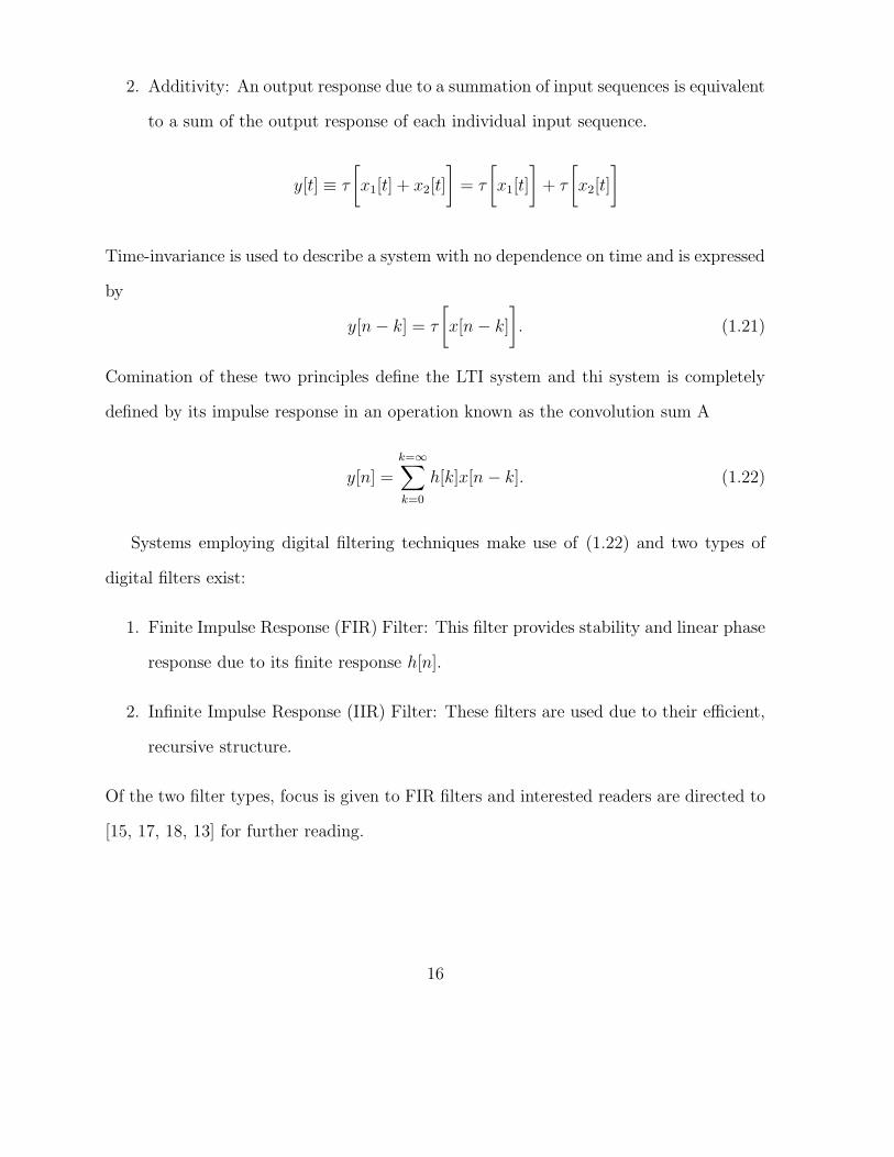
1.3.3 Multirate Systems
Decimation, or down-sampling of a signal, is a process in which the sampling rate is
reduced by an integer factor D. To prevent aliasing, a filter is typically used to limit
bandwidth to the Nyquist rate of the decimated sampling rate. To illustrate this concept,
imagine a signal with a frequency response shown in Figure 1.15. If the original sample
Figure 1.15: Image bandwidth
rate were ωs, the decimated sample rate becomes ωD = ωs/D. To prevent aliasing at the
down-sampled rate, a filter with frequency response
HD(ω) =
1 −πD
≤ ω ≤ πD
0 elsewhere
(1.23)
is required. This filter is shown in Figure 1.16. After filtering, decimation reduces image
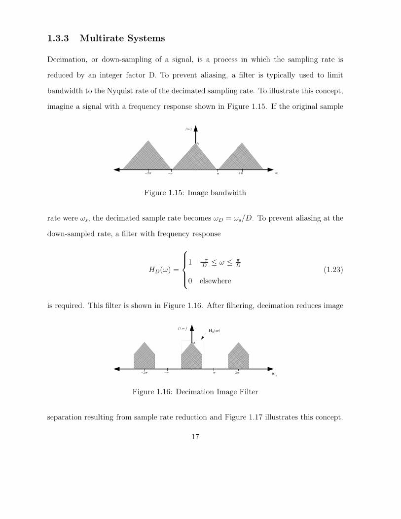
Figure 1.16: Decimation Image Filter
separation resulting from sample rate reduction and Figure 1.17 illustrates this concept.
17
A block diagram of this filter is shown in Figure 1.23. where v[n] is the convolution sum
Figure 1.17: Resulting spectrum from decimation
Figure 1.18: Decimation Block Diagram
of the input sequence with the unit sample response of the filter.
v[n] =∞
∑
k=0
h[k]x[n − k]. (1.24)
The result in Equation (1.24) is decimated by D producing the output y[m], where m
represents the decimated samples
n = mD (1.25)
The resulting output is
y[m] =
∞∑
k=0
h[k]x[mD − k]. (1.26)
One of the most commonly used applications of decimation is known as oversampling.
Referring back to (1.14), it was shown that quantization noise power was a constant quan-
18
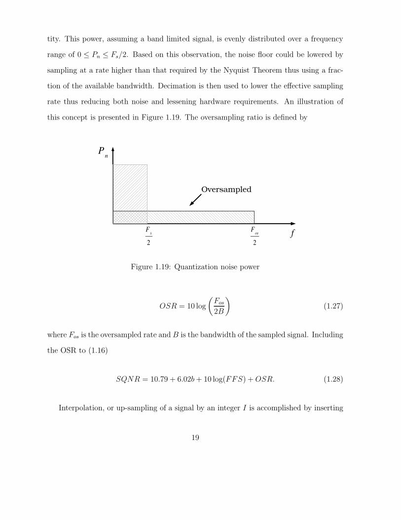
tity. This power, assuming a band limited signal, is evenly distributed over a frequency
range of 0 ≤ Pn ≤ Fs/2. Based on this observation, the noise floor could be lowered by
sampling at a rate higher than that required by the Nyquist Theorem thus using a frac-
tion of the available bandwidth. Decimation is then used to lower the effective sampling
rate thus reducing both noise and lessening hardware requirements. An illustration of
this concept is presented in Figure 1.19. The oversampling ratio is defined by
Figure 1.19: Quantization noise power
OSR = 10 log
(
Fos
2B
)
(1.27)
where Fos is the oversampled rate and B is the bandwidth of the sampled signal. Including
the OSR to (1.16)
SQNR = 10.79 + 6.02b + 10 log(FFS) + OSR. (1.28)
Interpolation, or up-sampling of a signal by an integer I is accomplished by inserting
19
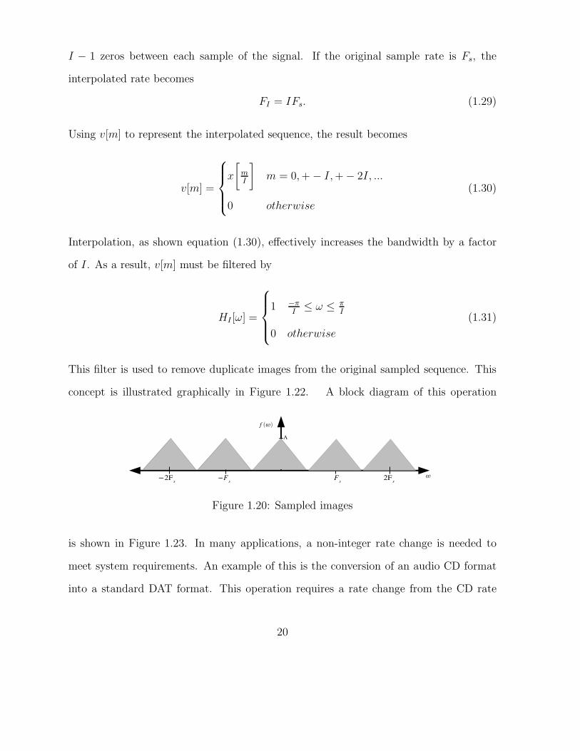
I − 1 zeros between each sample of the signal. If the original sample rate is Fs, the
interpolated rate becomes
FI = IFs. (1.29)
Using v[m] to represent the interpolated sequence, the result becomes
v[m] =
x
[
mI
]
m = 0, + − I, + − 2I, ...
0 otherwise
(1.30)
Interpolation, as shown equation (1.30), effectively increases the bandwidth by a factor
of I. As a result, v[m] must be filtered by
HI [ω] =
1 −πI
≤ ω ≤ πI
0 otherwise
(1.31)
This filter is used to remove duplicate images from the original sampled sequence. This
concept is illustrated graphically in Figure 1.22. A block diagram of this operation
Figure 1.20: Sampled images
is shown in Figure 1.23. In many applications, a non-integer rate change is needed to
meet system requirements. An example of this is the conversion of an audio CD format
into a standard DAT format. This operation requires a rate change from the CD rate
20
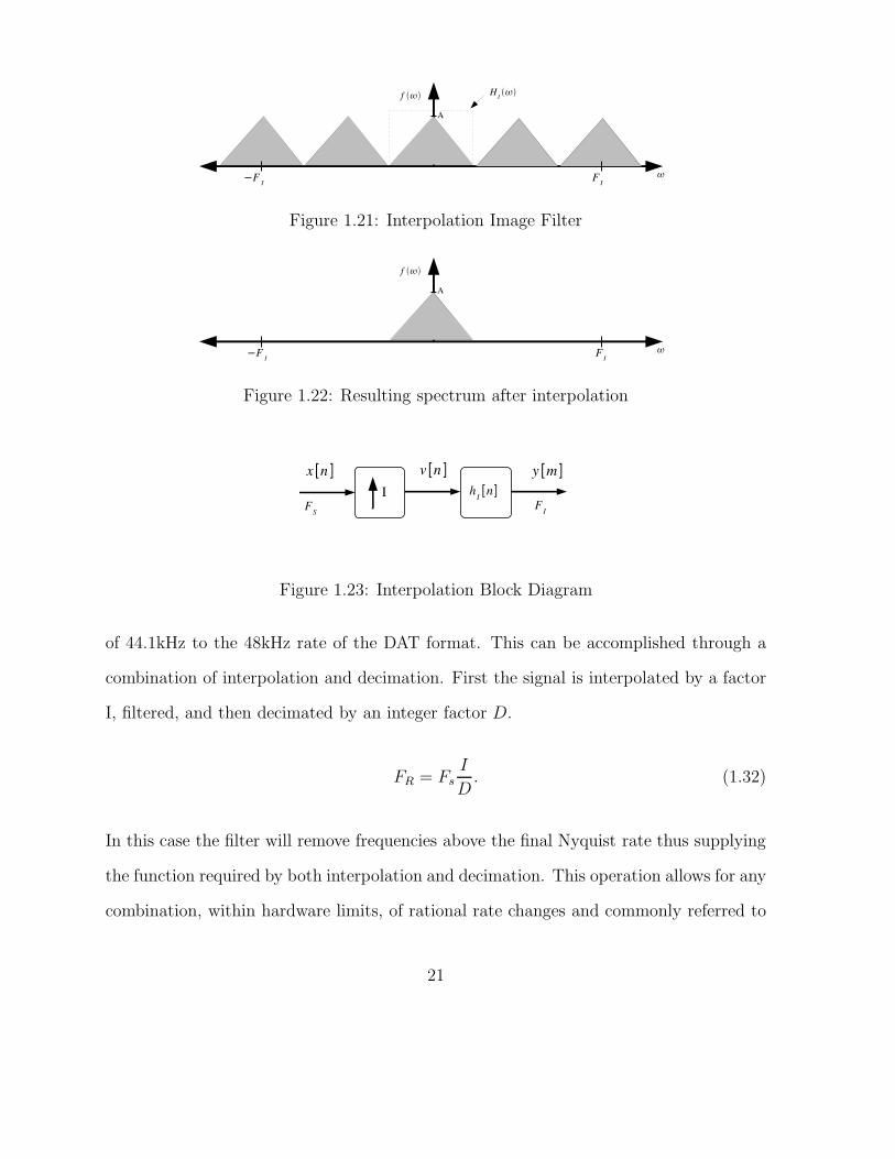
Figure 1.21: Interpolation Image Filter
Figure 1.22: Resulting spectrum after interpolation
Figure 1.23: Interpolation Block Diagram
of 44.1kHz to the 48kHz rate of the DAT format. This can be accomplished through a
combination of interpolation and decimation. First the signal is interpolated by a factor
I, filtered, and then decimated by an integer factor D.
FR = Fs
I
D. (1.32)
In this case the filter will remove frequencies above the final Nyquist rate thus supplying
the function required by both interpolation and decimation. This operation allows for any
combination, within hardware limits, of rational rate changes and commonly referred to
21
as a resampler. Using a combination of interpolation and decimation, a number of filter
techniques have been created to optimize performance in a DSP system. Application of
these filters will be discussed in chapter 2.
1.4 Software Analysis and Design
As the electronics industry and the resulting products advance in complexity, software
development is beginning to play a primary role in overall product design. The boundary
between electrical engineers and software engineers is diminishing rapidly [12]. In this
section an overview of object oriented programming (OOP) will be given along with a
review of relevant material from the Unified Modeling Language (UML). Together, these
tools provide a method for understanding and alleviating complexity in software design
as well as provide more robust software.
1.4.1 Object Oriented Programming
OOP was created out of a need to efficiently develop systems that were rapidly increasing
in both size and complexity. This section will provide a brief overview of the role OOP
plays in modern software design.
It is a known fact [11] that humans, in general, are only able to manage a maximum
of seven items simultaneously without error. Even small, well-understood systems can
present difficulties to the human mind. As a result, humans tend to reduce complexity
by partitioning a system into smaller, manageable pieces. In the case of top-down design,
systems are partioned by function; this is also known as procedural programming and
has been the most widely used method of design since the advent of modern comput-
ers. As system complexity increases, the top-down design methodology begins to expose
22
weakness in many areas such as: 1) readability, 2) maintainability, 3) adaptability, and
4) expandability The biggest problem with procedural programming, as seen by language
developers, is that responsibility is confined to one primary thread of control (main loop).
All of this responsibility in one place complicates coding and typically requires extensive
changes to accommodate small variations in design. Additionally, readability is reduced
thus making software maintainance more costly and time consuming. As an alternative,
researchers, in the 1970s, began to explore the idea of partioning a system through ob-
jects; and, by 1986, a number of object oriented languages were available. As seen from
the object oriented (OO) perspective, a system is composed of a collection of objects,
each with a well-defined behavior, that interact and collectively define the system. Par-
tioning a system through object decomposition results in many important characteristics.
Object re-use is made possible through inheritance, which is the ability for an object to
assume another object’s characteristics while reserving the ability to modify/add more
as needed. Encapsulation, the ability to hide complexity from the user, is possible by
exposing the object’s interface while hiding the inner complexity. In addition, the system
becomes easily adaptable/expandable since changes are made to the required object. The
abililty to understand and maintain the system is lessened due to well-defined boundaries
between objects. Of the many languages available for OOP, C++, due to widespread use
and support for graphical user interfaces (GUI), was chosen for this project. Interested
readers are referred to [4, 19] for complete coverage of OO analysis and design.
1.4.2 Unified Modeling Language
The UML is a graphical modeling system created to aid in the design of complex Object
Oriented based software systems. One of the most important uses of this modeling
23

language is its ability to bridge the gap between the software user and the software
developer. Strong communication between the system user and the developer is the most
important concept determining the success or failure of a design. The UML fills this gap
by abstracting system complexity into a set of interfaces and interactions, which can be
reasonably understood with minimal effort. This benefits not only the user of a complex
software system but also aids in the design of such systems by reducing complex object
interactions into a visual representation. The UML was released to the public in 1997 by
the Object Management Group (OMG) and has seen many revisions over time. Use of
the UML, as it relates to this thesis, is limited to a small subset of diagrams that were
found most suitable for this design. The following diagrams will be used:
1. Use Case: Illustrate interactions between the system’s users and the system itself.
This is used at the beginning of a design to gather all user interactions with the
system; and, consequently build a list of system requirements.
2. Class Diagram: Used to illustrate interactions between a collection of objects in the
system. They are also used to provide a list of properties and methods available to
each class.
3. Activity Diagram: Provide insight into the operation of a subset of the system
or an overview of the entire system. These diagrams resemble flow charts used
in procedural modeling but provide methods for illustrating concurrent activity
commonly seen in OO systems.
4. Composite Structure: Depict a broad view of a class by displaying the class inter-
face along with a description of components functioning inside the class. This is
accomplished by displaying the class’s internal functions using smaller blocks.
24
Chapter 2
System Analysis and Design
Implementation of any design begins with a complete definition of the problem followed
by a method of action to achieve the desired solution. This design used an object ori-
ented methodology and was chosen based on the ability of OO design to efficiently man-
age complexity and make the system resilient to change. Within the OO paradigm, an
overwhelming number of techniques and approaches exist and more than one were im-
plemented in this design. This section will discuss aspects of the system from a design
perspective. Both hardware and software discussions are combined to better communi-
cate their dependence. To begin, a precise definition of the problem domain, with the
help of domain experts, is the first stage of design known as requirements analysis[6]. The
sections that follow will discuss the techniques used to analyze, model, and implement
the design. Detailed discussion of both hardware and software are combined to better
communicate their interdependence.
25

2.1 Requirements Analysis
Definition of the system’s capabilities and features are best defined by users (domain
experts) of the system. A preliminary list of requirements were created as a first step in
the design process:
1. Users are typically visiting scientists and will receive limited assistance from staff.
2. Users need the ability to configure the system to meet their own specifications.
3. System configuration should be stored for later re-use.
4. Multiple configurations, cycled at predetermined intervals, are sometimes necessary
for a single experiment.
5. The system will use the Linux Operating System.
6. Some experiments require large bandwidths and high storage rates.
7. Minimal real-time processing and plotting tools are necessary to ensure proper setup
and equipment function.
8. Telescope position and sytem time are broadcast (multicast) on the network and
must be processed and stored.
9. A standard file format will be required for data storage and retrieval.
10. Software should be able to accommodate newer hardware revisions with minimal
effort.
11. Documentation must be written to assist both developers and users.
26
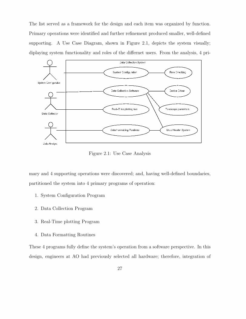
The list served as a framework for the design and each item was organized by function.
Primary operations were identified and further refinement produced smaller, well-defined
supporting. A Use Case Diagram, shown in Figure 2.1, depicts the system visually;
diplaying system functionality and roles of the differnet users. From the analysis, 4 pri-
Figure 2.1: Use Case Analysis
mary and 4 supporting operations were discovered; and, having well-defined boundaries,
partitioned the system into 4 primary programs of operation:
1. System Configuration Program
2. Data Collection Program
3. Real-Time plotting Program
4. Data Formatting Routines
These 4 programs fully define the system’s operation from a software perspective. In this
design, engineers at AO had previously selected all hardware; therefore, integration of
27
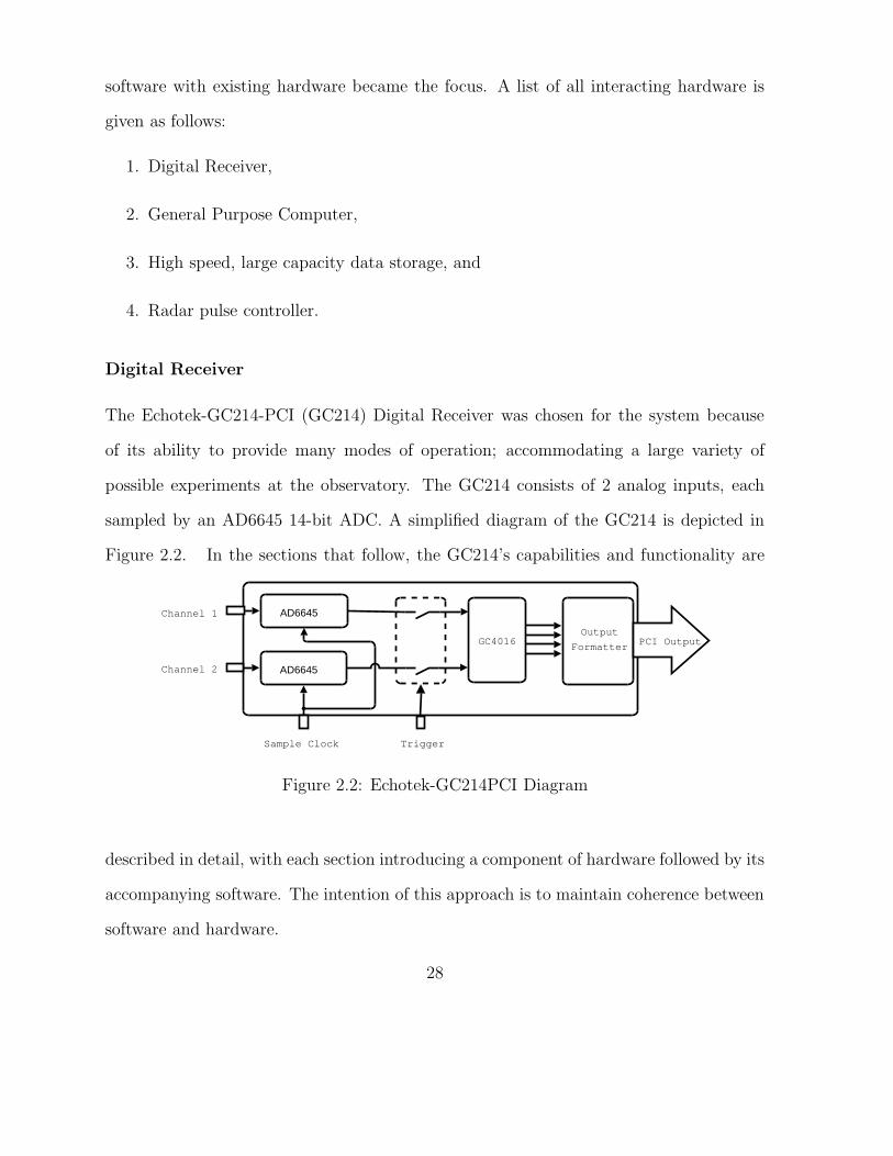
software with existing hardware became the focus. A list of all interacting hardware is
given as follows:
1. Digital Receiver,
2. General Purpose Computer,
3. High speed, large capacity data storage, and
4. Radar pulse controller.
Digital Receiver
The Echotek-GC214-PCI (GC214) Digital Receiver was chosen for the system because
of its ability to provide many modes of operation; accommodating a large variety of
possible experiments at the observatory. The GC214 consists of 2 analog inputs, each
sampled by an AD6645 14-bit ADC. A simplified diagram of the GC214 is depicted in
Figure 2.2. In the sections that follow, the GC214’s capabilities and functionality are
AD6645
AD6645
Channel 1
Channel 2
Sample Clock Trigger
GC4016Output
Formatter PCI Output
Figure 2.2: Echotek-GC214PCI Diagram
described in detail, with each section introducing a component of hardware followed by its
accompanying software. The intention of this approach is to maintain coherence between
software and hardware.
28
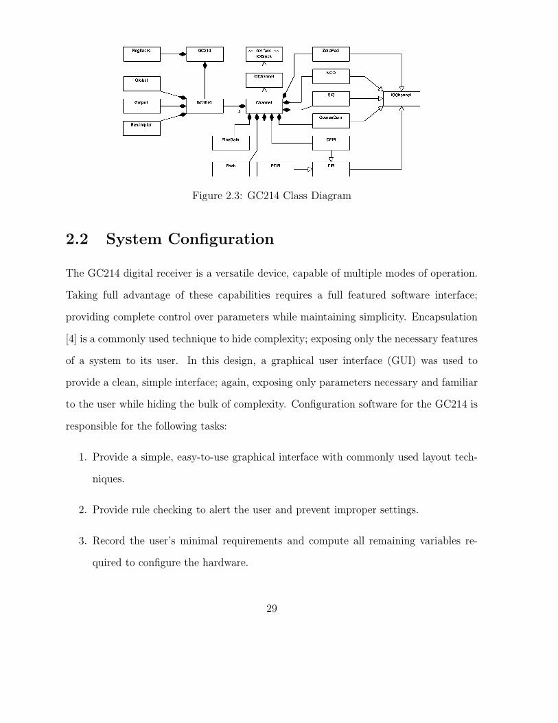
Figure 2.3: GC214 Class Diagram
2.2 System Configuration
The GC214 digital receiver is a versatile device, capable of multiple modes of operation.
Taking full advantage of these capabilities requires a full featured software interface;
providing complete control over parameters while maintaining simplicity. Encapsulation
[4] is a commonly used technique to hide complexity; exposing only the necessary features
of a system to its user. In this design, a graphical user interface (GUI) was used to
provide a clean, simple interface; again, exposing only parameters necessary and familiar
to the user while hiding the bulk of complexity. Configuration software for the GC214 is
responsible for the following tasks:
1. Provide a simple, easy-to-use graphical interface with commonly used layout tech-
niques.
2. Provide rule checking to alert the user and prevent improper settings.
3. Record the user’s minimal requirements and compute all remaining variables re-
quired to configure the hardware.
29
Additionally, a key component of this design was to produce a system resilient to change;
meaning that hardware upgrades would require minimal alterations to software. A num-
ber of components are needed to successfully perform all tasks required of a Digital
Receiver. A break-down of the GC214 is shown in Figure 2.3 and displays components
directly involved with system configuration. The GC4016 Digital Down Converter in-
tegrated circuit (IC) [21] is the primary component on the GC214. The GC4016 is
an Application Specific Integrated Circuit (ASIC) used to perform all data processing.
The GC4016 consists of 4 independent processing channels that perform signal down-
conversion, filtering, and data rate adjustments. Each of the 4 channels can operate
independently or can be combined to increase channel band-width. The GC4016, by
design, contains modules with well defined boundaries making it suitable for object de-
composition. Each of the modules, as stated in the manual [21], were used as objects in
software:
1. Input Format
2. ZeroPadding
3. Numerically Controlled Oscillator (NCO)
4. Cascaded Integrated Comb Filter (CIC)
5. Coarse Gain
6. 21 Tap Finite Impulse Response Filter I (CFIR)
7. 63 Tap Finite Impulse Response Filter II (PFIR)
8. Fine Gain
30
ZeroPad CICCoarse
GainCFIR PFIR
Fine
Gain
14-bit
Data Input
24-bit
Data Output
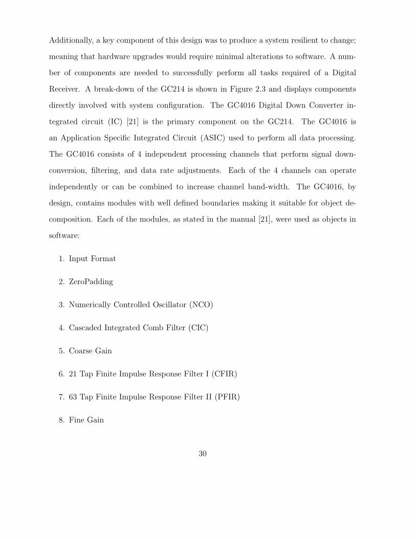
Figure 2.4: GC4016 Channel
9. Resampler
In the GC4016 datasheet [21], both Input Format and Resampler modules are mem-
bers of the channel. Further analysis revealed that the modules responsibilities were
common to all channels, therefore these modules were separated from the channel. This
separation produced classes that were more cohesive and loosely coupled. The Channel
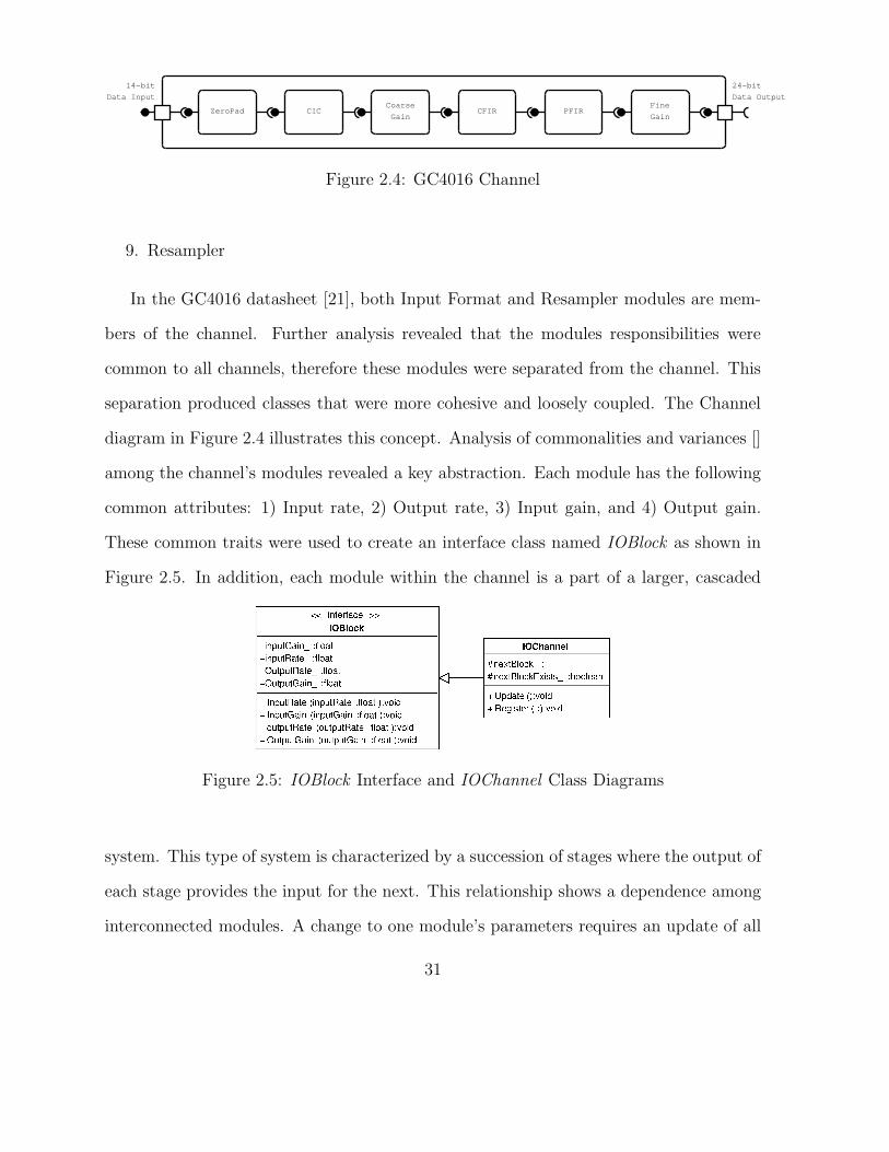
diagram in Figure 2.4 illustrates this concept. Analysis of commonalities and variances []
among the channel’s modules revealed a key abstraction. Each module has the following
common attributes: 1) Input rate, 2) Output rate, 3) Input gain, and 4) Output gain.
These common traits were used to create an interface class named IOBlock as shown in
Figure 2.5. In addition, each module within the channel is a part of a larger, cascaded
Figure 2.5: IOBlock Interface and IOChannel Class Diagrams
system. This type of system is characterized by a succession of stages where the output of
each stage provides the input for the next. This relationship shows a dependence among
interconnected modules. A change to one module’s parameters requires an update of all
31
modules that follow. This behavior was implemented by creating an abstract class named
IOChannel which inherits the IOBlock interface. Two methods were created to emulate
the cascading system as shown in Figure 2.5. Each object must register the next object
in the system via a base class pointer. Changes to a module invoke its Update member
which in turn calls its registered object’s Update member. Each subsequent module is
synchronized in this manner. Preceding stages are unaffected by this operation. Declar-
ing the Update member virtual allows derived classes to implement custom behavior.
Each module in the GC4016 channel inherits the IOChannel class.
ZeroPad Module
The first stage in the GC4016’s channel is the zero pad function. Zero padding is a
technique used to match the input data rate and the sample clock rate when the data
rate operates at a lower rate. Zeros are inserted between each input sample. From the
sample clock’s perspective, the input data rate is increased. Due to the apparent rate
increase, the user is able to choose a lower input rate. To ensure proper operation, the
input rate must meet specifications given by
InputRate =fclk
nzero + 1, (2.1)
where nzero is the number of zeros to insert. Valid values are integers ranging from 0
to 15. Input rates as low as fclk/16 are possible. Time Domain Multiplexing (TDM) is
another application requiring zero padding. In this application multiple channels of data
are serialized into a single data stream, separated by time. In this system, nzero is set to
the number of data channels. The zero pad function uses programmable synchronization
and, in the case of TDM, is required to sample the desired data channel. The zero pad
32
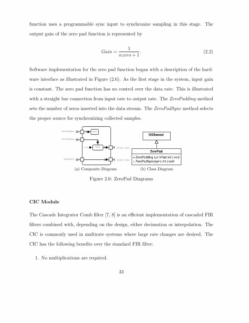
function uses a programmable sync input to synchronize sampling in this stage. The
output gain of the zero pad function is represented by
Gain =1
nzero + 1. (2.2)
Software implementation for the zero pad function began with a description of the hard-
ware interface as illustrated in Figure (2.6). As the first stage in the system, input gain
is constant. The zero pad function has no control over the data rate. This is illustrated
with a straight bar connection from input rate to output rate. The ZeroPadding method
sets the number of zeros inserted into the data stream. The ZeroPadSync method selects
the proper source for synchronizing collected samples.
ZeroPadSync
ZeroPadding
InputRate
Output Gain
Output Rate
Sync
Gain1.00
(a) Composite Diagram (b) Class Diagram
Figure 2.6: ZeroPad Diagrams
CIC Module
The Cascade Integrator Comb filter [7, 8] is an efficient implementation of cascaded FIR
filters combined with, depending on the design, either decimation or interpolation. The
CIC is commonly used in multirate systems where large rate changes are desired. The
CIC has the following benefits over the standard FIR filter:
1. No multiplications are required.
33
2. No storage required for filter coefficients.
The FIR transfer function has the form
H(z) =
K−1∑
k=0
h[k]z−k (2.3)
where h is the impulse response kernel, k is the delay, and K is the number of coefficients.
Noting that (2.3) is a finite geometric series, the basic structure of a single stage CIC is
realized from the latter part of (2.4).
SK =K−1∑
k=0
ark ≡ a(1 − rK)
1 − r(2.4)
Setting coefficients to unity and letting r = z−1, the CIC transfer function becomes
H(z) =
[
(1 − z−RM )
1 − z−1
]N
(2.5)
where R is the decimation factor, M is differential delay, and N is the number of cascaded
stages. The CIC implementation uses a combination of integrators and comb stages,
combined with a rate changing mechanism such as interpolation or decimation. A single
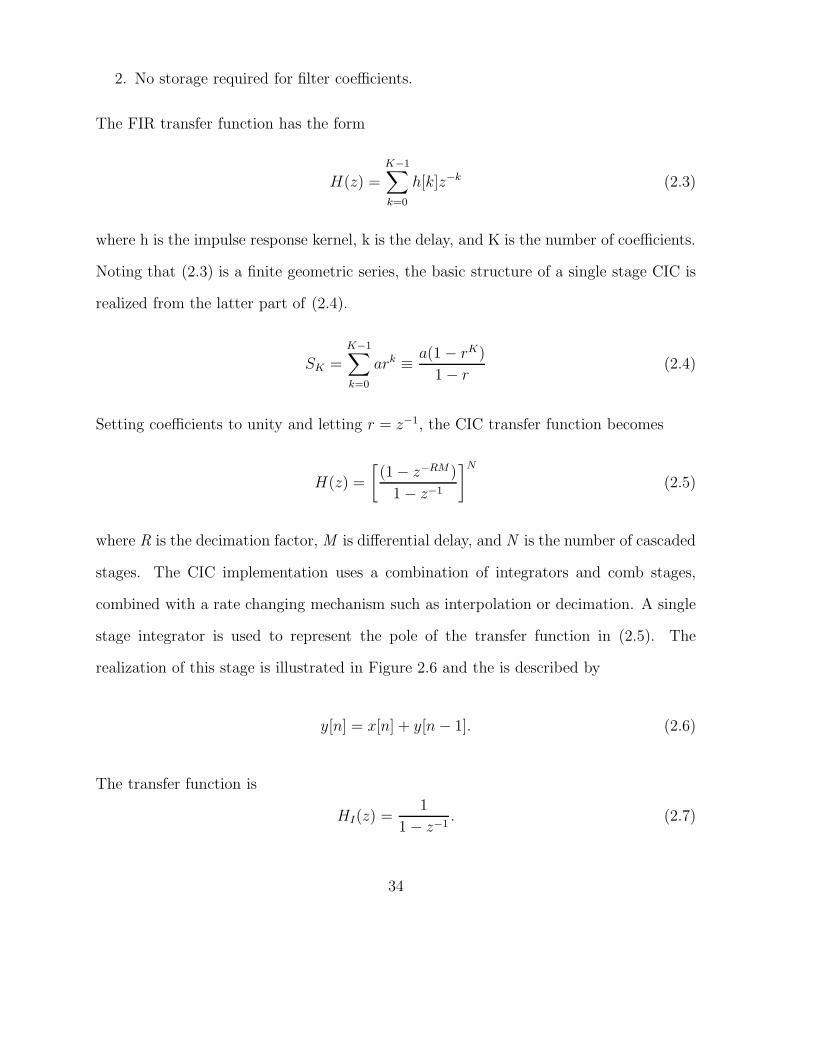
stage integrator is used to represent the pole of the transfer function in (2.5). The
realization of this stage is illustrated in Figure 2.6 and the is described by
y[n] = x[n] + y[n − 1]. (2.6)
The transfer function is
HI(z) =1
1 − z−1. (2.7)
34
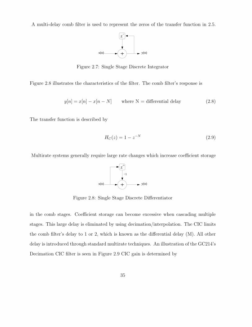
A multi-delay comb filter is used to represent the zeros of the transfer function in 2.5.
x(n) y(n)
Z−1
Figure 2.7: Single Stage Discrete Integrator
Figure 2.8 illustrates the characteristics of the filter. The comb filter’s response is
y[n] = x[n] − x[n − N ] where N = differential delay (2.8)
The transfer function is described by
HC(z) = 1 − z−N (2.9)
Multirate systems generally require large rate changes which increase coefficient storage
−1
Z−N
x(n) y(n)
Figure 2.8: Single Stage Discrete Differentiator
in the comb stages. Coefficient storage can become excessive when cascading multiple
stages. This large delay is eliminated by using decimation/interpolation. The CIC limits
the comb filter’s delay to 1 or 2, which is known as the differential delay (M). All other
delay is introduced through standard multirate techniques. An illustration of the GC214’s
Decimation CIC filter is seen in Figure 2.9 CIC gain is determined by
35
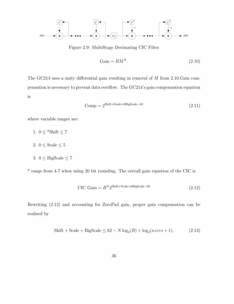
R
Z−1
Z−1
x(n) y(n)
−1
Z−M
−1
Z−M
Figure 2.9: MultiStage Decimating CIC Filter
Gain = RMN . (2.10)
The GC214 uses a unity differential gain resulting in removal of M from 2.10.Gain com-
pensation is necessary to prevent data overflow. The GC214’s gain compensation equation
is
Comp = 2Shift+Scale+6BigScale−62 (2.11)
where variable ranges are:
1. 0 ≤ *Shift ≤ 7
2. 0 ≤ Scale ≤ 5
3. 0 ≤ BigScale ≤ 7
* range from 4-7 when using 20 bit rounding. The overall gain equation of the CIC is
CIC Gain = RN2Shift+Scale+6BigScale−62 (2.12)
Rewriting (2.12) and accounting for ZeroPad gain, proper gain compensation can be
realized by
Shift + Scale + BigScale ≤ 62 − N log2(R) + log2(nzero + 1). (2.13)
36

Violation of this rule will result in undetected data overflow and an automated algorithm
was implemented to prevent this occurrence. The CIC module is derived from IOChan-
nel and is responsible for the gain, decimation, and multichannel options that will be
discussed in a later section. The CIC module class diagram is illustrated in Figure 2.10.
The CIC module interface is shown in Figure 2.10. Gain synchronization is provided via
InputGain
Decimation
Input Rate
Output Gain
Output Rate
1/Decimation
RoundNormalize
Set20BitRoundMode
IOnly
QOnly
Multi
Channel
NegCtl
SplitIQ
Sync
GainSync
(a) Composite Diagram (b) Class Diagram
Figure 2.10: CIC Diagrams
the GainSync member. Output data can be rounded to 16 or 20 bits, with decimation
greater than 3104 limited to 16-bit rounding. A gain normalization algorithm is provided
to optimize variables for unity gain, and prevent data clipping due to improper settings.
The CIC’s Normalize member optimizes: 1) shift, 2) scale, 3) and bigScale variables.
The code segment in 2.1 illustrates the algorithm.
void CIC : : Normalize ( )
s h i f t = 7 ; b igSca l e = 0 ; s c a l e = 5 ;
f loat r ightVa lue = 62 .0 f − ( 5 . 0 f ∗ l o g ( static cast<f loat >(dec imation ) ) +log ( InputGain ( ) ) ) / l og ( 2 . 0 f ) ;
f loat l e f tVa lu e = s c a l e + s h i f t + 6 .0 f ∗ b igSca l e ;
37
while ( ( l e f tVa lu e < r ightVa lue ) && ( b igSca l e != 7 .0 f ) )++bigSca l e ; l e f tVa lu e += 6 .0 f ;
while ( ( l e f tVa lu e > r ightVa lue ) && ( s h i f t != 4 .0 f ) )−−s h i f t ; −−l e f tVa lu e ;
while ( ( l e f tVa lu e > r ightVa lue ) && ( s c a l e != 0 .0 f ) )−−s c a l e ; −−l e f tVa lu e ;
while ( ( l e f tVa lu e > r ightVa lue ) && ( s h i f t != 0 .0 f ) && ! mix20b )−−s h i f t ; −−l e f tVa lu e ;
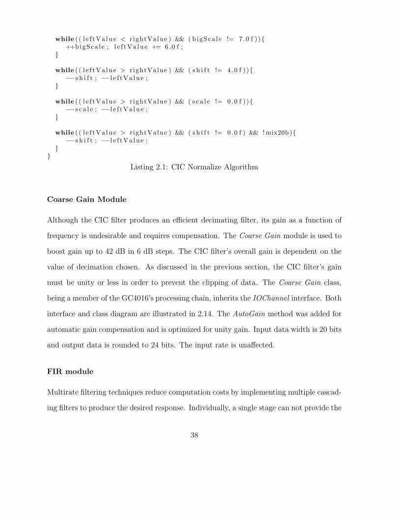
Listing 2.1: CIC Normalize Algorithm
Coarse Gain Module
Although the CIC filter produces an efficient decimating filter, its gain as a function of
frequency is undesirable and requires compensation. The Coarse Gain module is used to
boost gain up to 42 dB in 6 dB steps. The CIC filter’s overall gain is dependent on the
value of decimation chosen. As discussed in the previous section, the CIC filter’s gain
must be unity or less in order to prevent the clipping of data. The Coarse Gain class,
being a member of the GC4016’s processing chain, inherits the IOChannel interface. Both
interface and class diagram are illustrated in 2.14. The AutoGain method was added for
automatic gain compensation and is optimized for unity gain. Input data width is 20 bits
and output data is rounded to 24 bits. The input rate is unaffected.
FIR module
Multirate filtering techniques reduce computation costs by implementing multiple cascad-
ing filters to produce the desired response. Individually, a single stage can not provide the
38

CoarseGain
AutoGain
InputGain
InputRate
OutputGain
OutputRate
Auto Adjust
Gain
Gain Selector
(a) Composite Diagram (b) Class Diagram
Figure 2.11: Coarse Gain Diagrams
desired response due to the limited number of coefficients used to represent the transfer
function. Instead, each stage provides a relaxed transition band and followed by deci-
mation which effectively lowers the filter’s data rate, thus providing an a good response
without a large number of filter coefficients. A typical FIR response is
H [n] =
N∑
k=0
h[n]x[n − k] (2.14)
where n is the sample number, k is the delay, and N is the length of the filter.
CreateFilter
LoadDefaultFilter
CustomFilter
Output Gain
Output Rate
Filter
Select
Filter
Taps
Sum
Copy
InitFilters
InputRate
InputGain
Update
PrintTaps
Normalize
(a) Composite Diagram (b) Class Diagram
Figure 2.12: FIR Diagrams
39
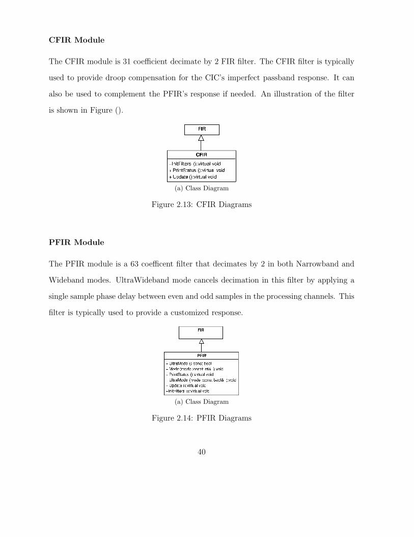
CFIR Module
The CFIR module is 31 coefficient decimate by 2 FIR filter. The CFIR filter is typically
used to provide droop compensation for the CIC’s imperfect passband response. It can
also be used to complement the PFIR’s response if needed. An illustration of the filter
is shown in Figure ().
(a) Class Diagram
Figure 2.13: CFIR Diagrams
PFIR Module
The PFIR module is a 63 coefficent filter that decimates by 2 in both Narrowband and
Wideband modes. UltraWideband mode cancels decimation in this filter by applying a
single sample phase delay between even and odd samples in the processing channels. This
filter is typically used to provide a customized response.
(a) Class Diagram
Figure 2.14: PFIR Diagrams
40
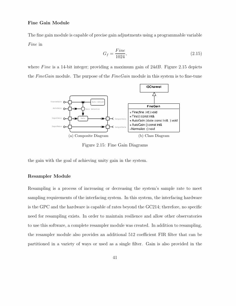
Fine Gain Module
The fine gain module is capable of precise gain adjustments using a programmable variable
Fine in
Gf =Fine
1024, (2.15)
where Fine is a 14-bit integer; providing a maximum gain of 24dB. Figure 2.15 depicts
the FineGain module. The purpose of the FineGain module in this system is to fine-tune
CoarseGain
AutoGain
InputGain
InputRate
OutputGain
OutputRate
Auto Adjust
Gain
Gain Selector
(a) Composite Diagram (b) Class Diagram
Figure 2.15: Fine Gain Diagrams
the gain with the goal of achieving unity gain in the system.
Resampler Module
Resampling is a process of increasing or decreasing the system’s sample rate to meet
sampling requirements of the interfacing system. In this system, the interfacing hardware
is the GPC and the hardware is capable of rates beyond the GC214; therefore, no specific
need for resampling exists. In order to maintain resilience and allow other observatories
to use this software, a complete resampler module was created. In addition to resampling,
the resampler module also provides an additional 512 coefficient FIR filter that can be
partitioned in a variety of ways or used as a single filter. Gain is also provided in the
41
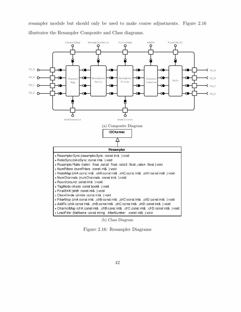
resampler module but should only be used to make coarse adjustments. Figure 2.16
illustrates the Resampler Composite and Class diagrams.
CH_A
CH_B
CH_C
CH_D
Channel
Map
Resampler
Ratio
Resampler
FilterChannel
CombineGain
CH_A
CH_B
CH_C
CH_D
ChannelMap ResamplerRatio AddTo FinalShiftFilterMap
NumFiltersNumChannels
(a) Composite Diagram
(b) Class Diagram
Figure 2.16: Resampler Diagrams
42
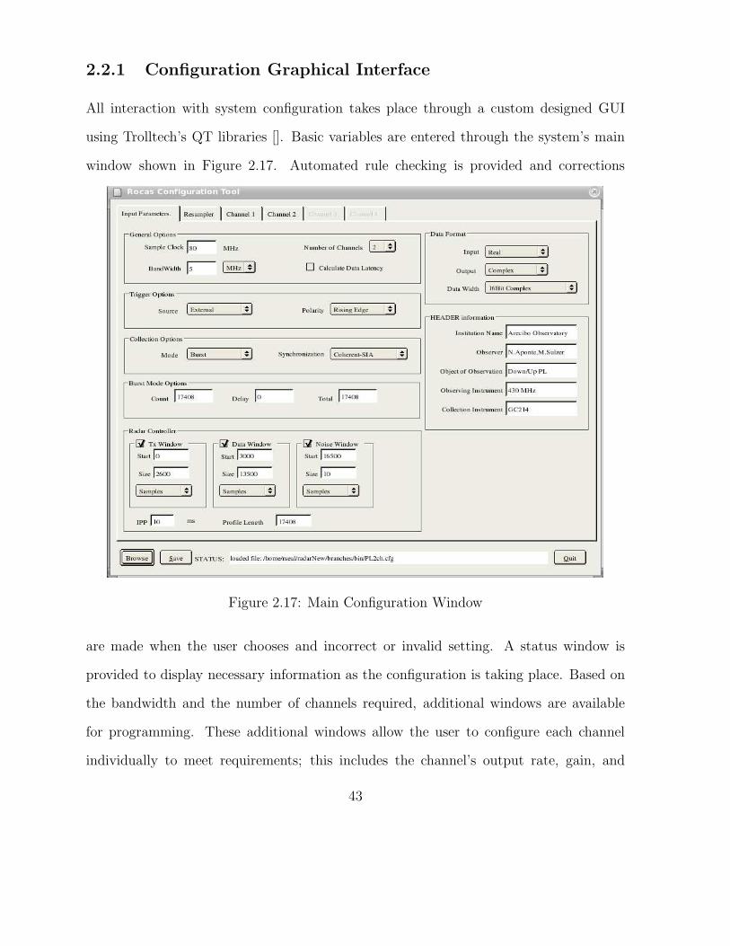
2.2.1 Configuration Graphical Interface
All interaction with system configuration takes place through a custom designed GUI
using Trolltech’s QT libraries []. Basic variables are entered through the system’s main
window shown in Figure 2.17. Automated rule checking is provided and corrections
Figure 2.17: Main Configuration Window
are made when the user chooses and incorrect or invalid setting. A status window is
provided to display necessary information as the configuration is taking place. Based on
the bandwidth and the number of channels required, additional windows are available
for programming. These additional windows allow the user to configure each channel
individually to meet requirements; this includes the channel’s output rate, gain, and
43
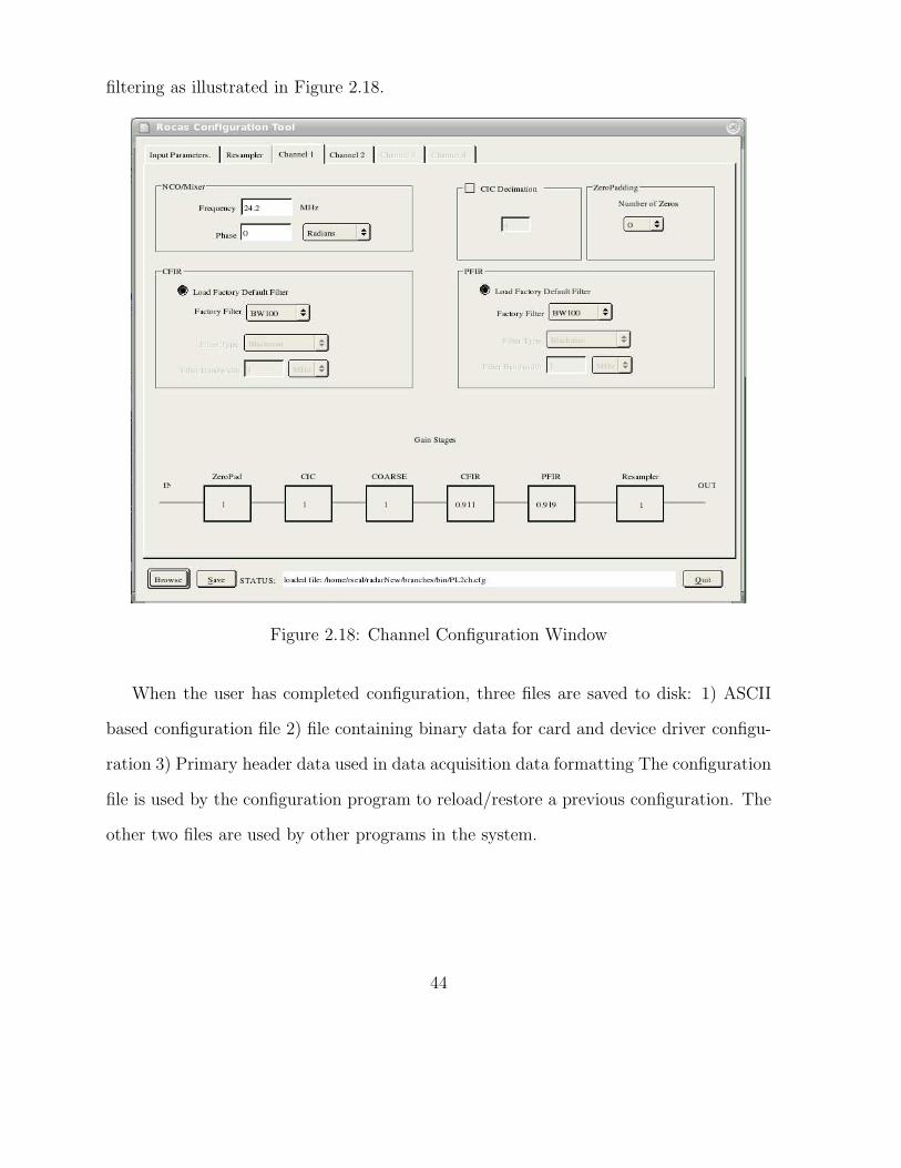
filtering as illustrated in Figure 2.18.
Figure 2.18: Channel Configuration Window
When the user has completed configuration, three files are saved to disk: 1) ASCII
based configuration file 2) file containing binary data for card and device driver configu-
ration 3) Primary header data used in data acquisition data formatting The configuration
file is used by the configuration program to reload/restore a previous configuration. The
other two files are used by other programs in the system.
44
2.3 Data Acquisition
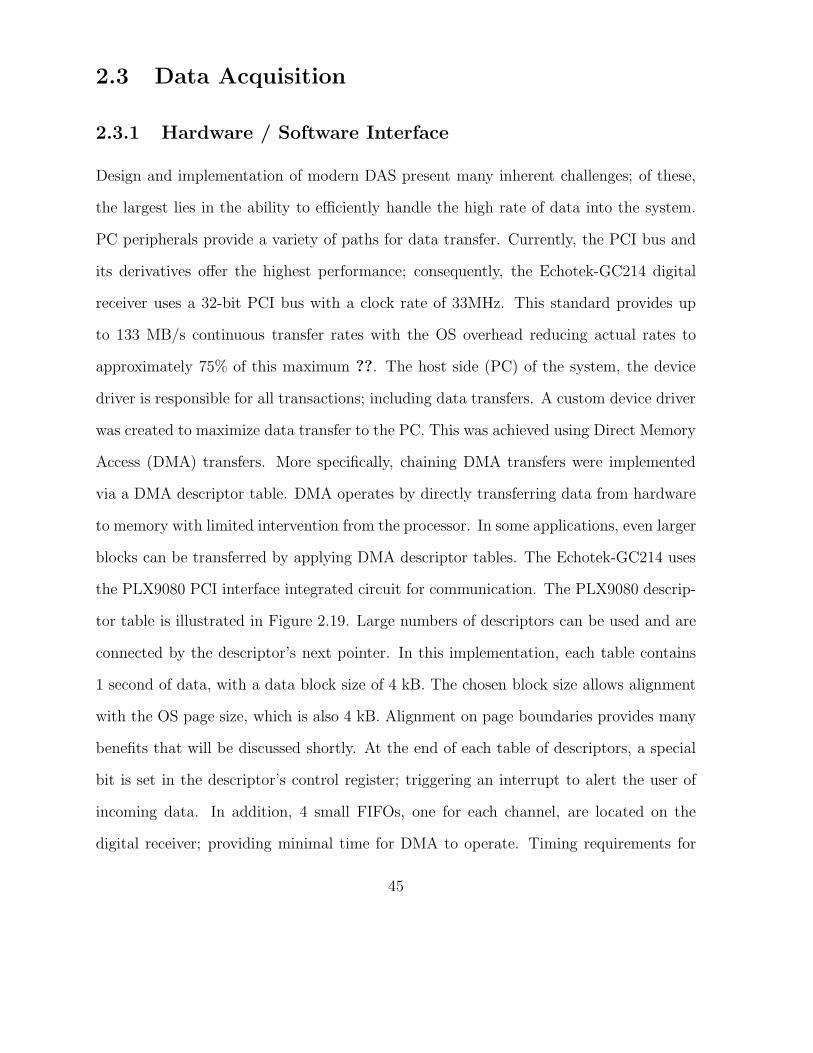
2.3.1 Hardware / Software Interface
Design and implementation of modern DAS present many inherent challenges; of these,
the largest lies in the ability to efficiently handle the high rate of data into the system.
PC peripherals provide a variety of paths for data transfer. Currently, the PCI bus and
its derivatives offer the highest performance; consequently, the Echotek-GC214 digital
receiver uses a 32-bit PCI bus with a clock rate of 33MHz. This standard provides up
to 133 MB/s continuous transfer rates with the OS overhead reducing actual rates to
approximately 75% of this maximum ??. The host side (PC) of the system, the device
driver is responsible for all transactions; including data transfers. A custom device driver
was created to maximize data transfer to the PC. This was achieved using Direct Memory
Access (DMA) transfers. More specifically, chaining DMA transfers were implemented
via a DMA descriptor table. DMA operates by directly transferring data from hardware
to memory with limited intervention from the processor. In some applications, even larger
blocks can be transferred by applying DMA descriptor tables. The Echotek-GC214 uses
the PLX9080 PCI interface integrated circuit for communication. The PLX9080 descrip-
tor table is illustrated in Figure 2.19. Large numbers of descriptors can be used and are
connected by the descriptor’s next pointer. In this implementation, each table contains
1 second of data, with a data block size of 4 kB. The chosen block size allows alignment
with the OS page size, which is also 4 kB. Alignment on page boundaries provides many
benefits that will be discussed shortly. At the end of each table of descriptors, a special
bit is set in the descriptor’s control register; triggering an interrupt to alert the user of
incoming data. In addition, 4 small FIFOs, one for each channel, are located on the
digital receiver; providing minimal time for DMA to operate. Timing requirements for
45

Figure 2.19: PLX9080 DMA Descriptor Layout
such systems are depicted in figure 2.20. Each of the FIFOs depicted in Figure 2.20
Figure 2.20: Echotek-GC214 FIFO Layout
are 64x32 kB in length, with each channel capable of transfer rates up to 9.54 MSPS.
To prevent data loss, maximum sustainable rates of 38.15 MSPS must be achieved. In
addition to data transfer, many other tasks are needed for full operation: 1) Partial se-
lection data for storage. 2) System verification using real-time data displays. 3) Header
information is to stored data. To fulfill the complete requirements of the system, a com-
bination of techniques were employed: 1) dual-layer buffer system utilizing both kernel
46
and user levels of the OS 2) the producer/consumer threading model 3) shared memory
via the tmpfs filesystem Dual-layer buffers are widely used in audio application software
and provide multiple buffers to mask system delays which would normally produce unac-
ceptable sound performance. In this particular system, a lower level set of buffers, called
DMA buffers, are allocated by the device driver; making these buffers kernel allocated
buffers. In many Operating Systems, two levels of priority are used when dealing with
interactions:
1. Kernel mode - this level is reserved for low level system management required by
the operating system. Device drivers are run in this mode; preventing the common
user from potentially damaging devices through direct hardware control.
2. User mode - this is the mode used by system users and application programmers.
The user interacts, as needed, with kernel mode through the use of well defined
system calls provided by the operating system.
The Echotek-GC214 device driver manages the kernel allocated DMA buffers and offers
user access using the mmap system call. The mmap function, known as memory mapping,
allows the user to map kernel allocated memory into user space using standard C language
file I/O functions. In order to minimize memory management at the kernel level, provide
real-time plotting capabilities, and provide flexibility to the user’s application software, a
secondary buffer system was allocated in user space. Additionally, this system utilizes the
Linux OS’s shared memory capabilities. Shared memory, as the name implies, allows a
user’s process (running program) to include the shared memory’s address space in its own
space; consequently, the user’s process can treat the memory as its own. A specialized
filesystem [16] called the tmpfs filesystem was used to provide a clean interface to shared
memory. This filesystem allows the user to create files in PC RAM using standard
47
function calls. Memory management is handled through a simple file I/O interface.
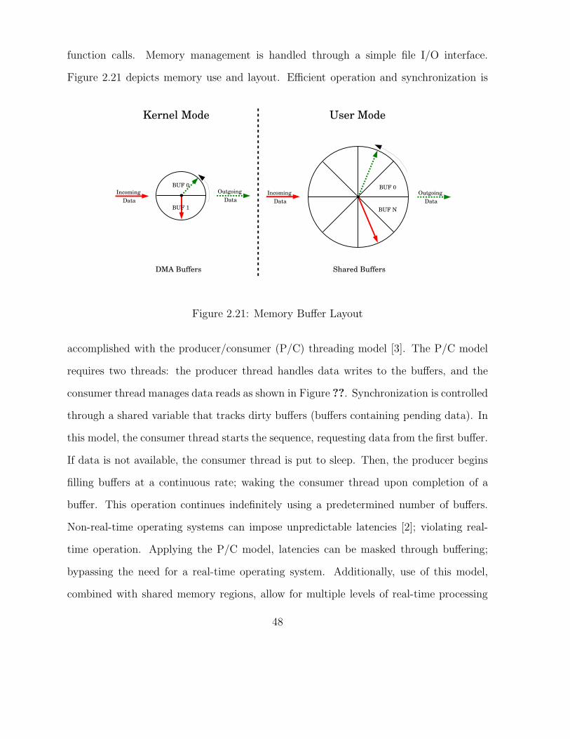
Figure 2.21 depicts memory use and layout. Efficient operation and synchronization is
Figure 2.21: Memory Buffer Layout
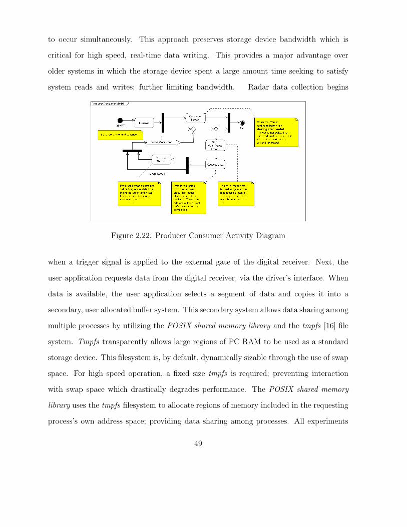
accomplished with the producer/consumer (P/C) threading model [3]. The P/C model
requires two threads: the producer thread handles data writes to the buffers, and the
consumer thread manages data reads as shown in Figure ??. Synchronization is controlled
through a shared variable that tracks dirty buffers (buffers containing pending data). In
this model, the consumer thread starts the sequence, requesting data from the first buffer.
If data is not available, the consumer thread is put to sleep. Then, the producer begins
filling buffers at a continuous rate; waking the consumer thread upon completion of a
buffer. This operation continues indefinitely using a predetermined number of buffers.
Non-real-time operating systems can impose unpredictable latencies [2]; violating real-
time operation. Applying the P/C model, latencies can be masked through buffering;
bypassing the need for a real-time operating system. Additionally, use of this model,
combined with shared memory regions, allow for multiple levels of real-time processing
48
to occur simultaneously. This approach preserves storage device bandwidth which is
critical for high speed, real-time data writing. This provides a major advantage over
older systems in which the storage device spent a large amount time seeking to satisfy
system reads and writes; further limiting bandwidth. Radar data collection begins
Figure 2.22: Producer Consumer Activity Diagram
when a trigger signal is applied to the external gate of the digital receiver. Next, the
user application requests data from the digital receiver, via the driver’s interface. When
data is available, the user application selects a segment of data and copies it into a
secondary, user allocated buffer system. This secondary system allows data sharing among
multiple processes by utilizing the POSIX shared memory library and the tmpfs [16] file
system. Tmpfs transparently allows large regions of PC RAM to be used as a standard
storage device. This filesystem is, by default, dynamically sizable through the use of swap
space. For high speed operation, a fixed size tmpfs is required; preventing interaction
with swap space which drastically degrades performance. The POSIX shared memory
library uses the tmpfs filesystem to allocate regions of memory included in the requesting
process’s own address space; providing data sharing among processes. All experiments
49
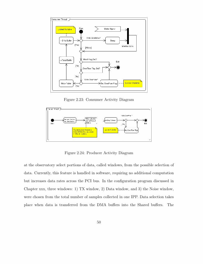
Figure 2.23: Consumer Activity Diagram
Figure 2.24: Producer Activity Diagram
at the observatory select portions of data, called windows, from the possible selection of
data. Currently, this feature is handled in software, requiring no additional computation
but increases data rates across the PCI bus. In the configuration program discussed in
Chapter xxx, three windows: 1) TX window, 2) Data window, and 3) the Noise window,
were chosen from the total number of samples collected in one IPP. Data selection takes
place when data is transferred from the DMA buffers into the Shared buffers. The
50
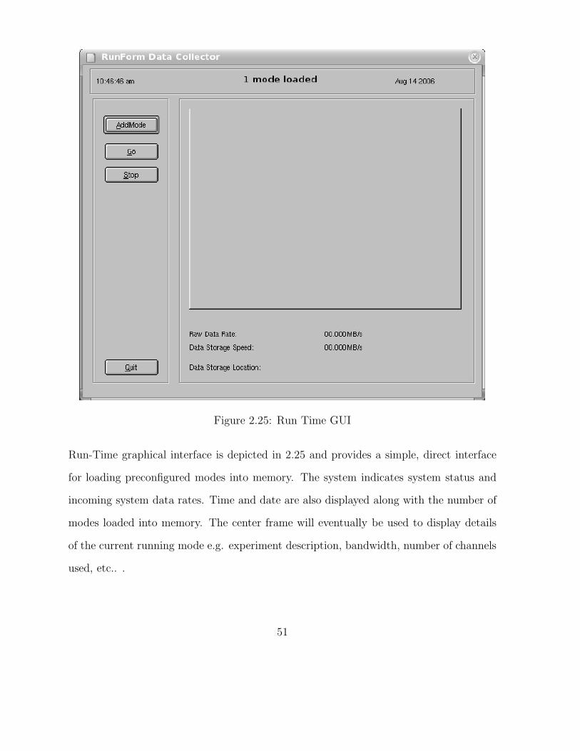
Figure 2.25: Run Time GUI
Run-Time graphical interface is depicted in 2.25 and provides a simple, direct interface
for loading preconfigured modes into memory. The system indicates system status and
incoming system data rates. Time and date are also displayed along with the number of
modes loaded into memory. The center frame will eventually be used to display details
of the current running mode e.g. experiment description, bandwidth, number of channels
used, etc.. .
51
2.4 Real-Time Data Display
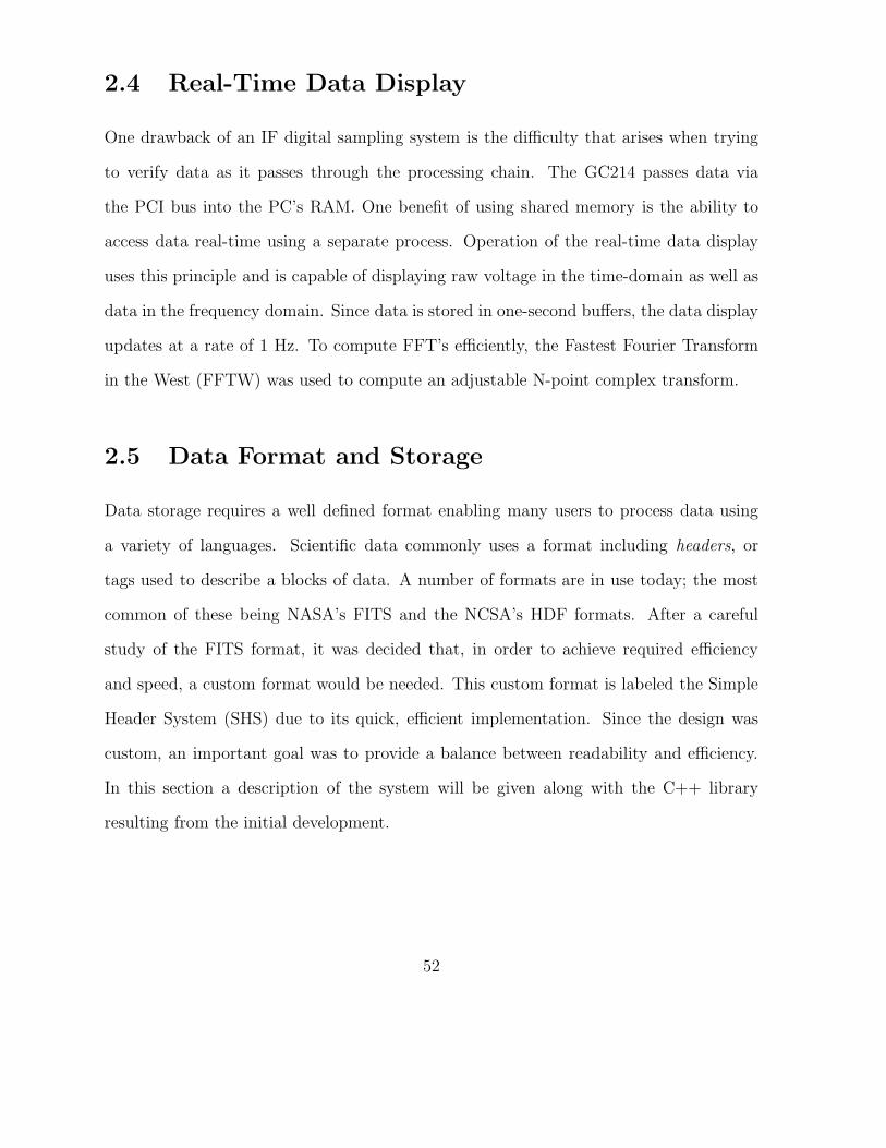
One drawback of an IF digital sampling system is the difficulty that arises when trying
to verify data as it passes through the processing chain. The GC214 passes data via
the PCI bus into the PC’s RAM. One benefit of using shared memory is the ability to
access data real-time using a separate process. Operation of the real-time data display
uses this principle and is capable of displaying raw voltage in the time-domain as well as
data in the frequency domain. Since data is stored in one-second buffers, the data display
updates at a rate of 1 Hz. To compute FFT’s efficiently, the Fastest Fourier Transform
in the West (FFTW) was used to compute an adjustable N-point complex transform.
2.5 Data Format and Storage
Data storage requires a well defined format enabling many users to process data using
a variety of languages. Scientific data commonly uses a format including headers, or
tags used to describe a blocks of data. A number of formats are in use today; the most
common of these being NASA’s FITS and the NCSA’s HDF formats. After a careful
study of the FITS format, it was decided that, in order to achieve required efficiency
and speed, a custom format would be needed. This custom format is labeled the Simple
Header System (SHS) due to its quick, efficient implementation. Since the design was
custom, an important goal was to provide a balance between readability and efficiency.
In this section a description of the system will be given along with the C++ library
resulting from the initial development.
52
File Name
Simple Header files (SHS), are defined by the .shs extension, and a data set consists of
multiple files sharing a common basename and an increasing index number starting from
000. A sample data set is depicted in ??.
1 testFile_000.shs
2 testFile_001.shs
3 testFile_002.shs
4 testFile_003.shs
5 testFile_004.shs
6 testFile_005.shs
7 testFile_006.shs
8 testFile_007.shs
Keyword
The purpose of the SHS structure is to fully describe all aspects of the data so that,
upon retrieval, all variables required for processing are available. Variables are described
using keywords. A keyword consists of four parts: (1) Name (2) Value (3) Type, and
(4) Comment. All keywords and delimiters in the SHS file are 96 bytes in length and are
in ASCII format. This provides negligable overhead and serves two important purposes:
1. The primary and first data header (described below) can be examined using com-
mand line tools (more,less,etc...). This provides a quick method for verification
without the need for specialized software.
2. Using ASCII for header information removes byte ordering dependence. This sim-
plifies header parsing when working with multiple platforms.
53
File Structure
Each SHS file consists of 3 primary structures:
1. Primary Header
This header is located at the beginning of each file in a data set. The information
is static and both fixed and custom keywords are present.
2. Data Header
The data header precedes every data table in a file and describes dynamic infor-
mation relevant to the table that follows. Multiple data tables exist in a single
file.
3. Data Table
Data Tables are blocks of data with a size defined by the user. Block size usually
corresponds to a particular boundary preferrable for processing. Tables can be
formatted in either ASCII or binary.
A visual summary is shown in Figure 2.26 and a complete description is given in the SHS
Headers section of this document. Each SHS file begins with a title, version, and author
section; followed by the license. This section is referred to as the file ID and provides a
method for verifying the file type and version of software used to create the file. Figure
2.27 illustrates the current file ID.
SHS Headers
SHS files contain two types of headers: 1) primary header and 2) data header. Together,
these headers fully describe both static and dynamic information related to the stored
data. Each header uses keywords to describe data and each follow a structered format
54
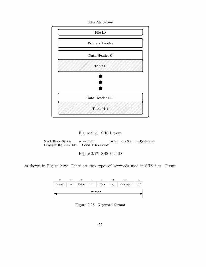
Figure 2.26: SHS Layout
Simple Header System version: 0.01 author: Ryan Seal <[email protected]>Copyright (C) 2005 GNU General Public License
Figure 2.27: SHS File ID
as shown in Figure 2.28: There are two types of keywords used in SHS files. Figure
Figure 2.28: Keyword format
55
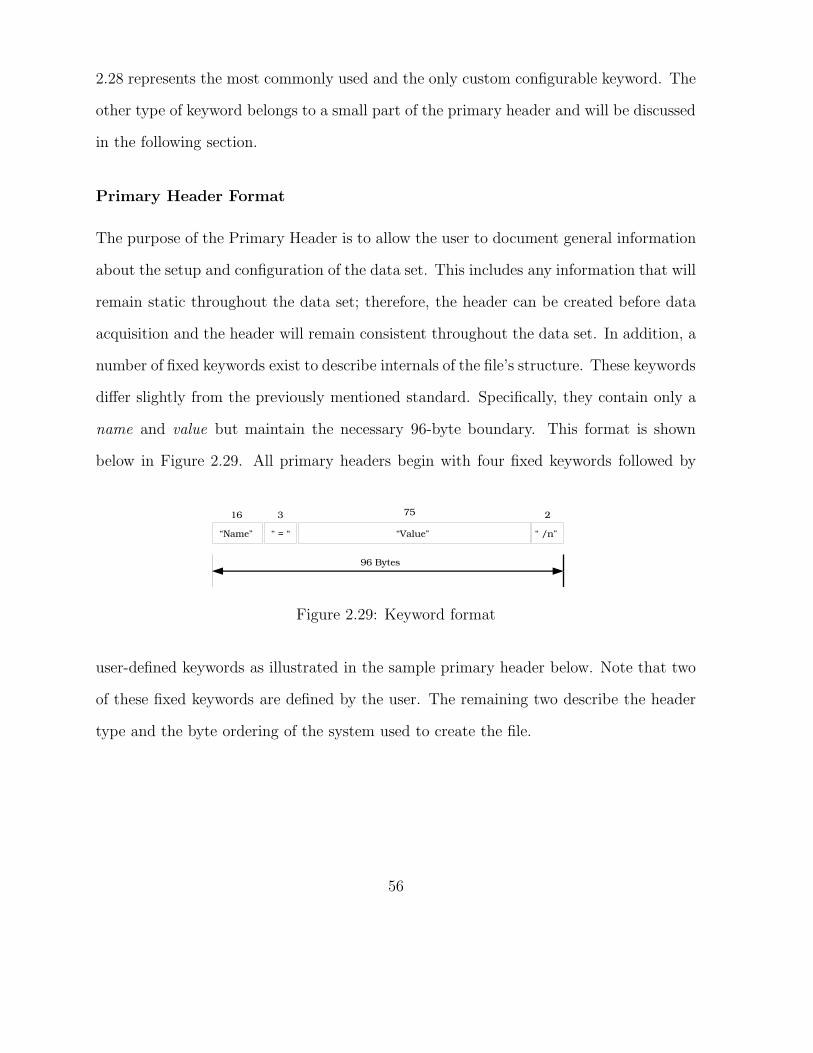
2.28 represents the most commonly used and the only custom configurable keyword. The
other type of keyword belongs to a small part of the primary header and will be discussed
in the following section.
Primary Header Format
The purpose of the Primary Header is to allow the user to document general information
about the setup and configuration of the data set. This includes any information that will
remain static throughout the data set; therefore, the header can be created before data
acquisition and the header will remain consistent throughout the data set. In addition, a
number of fixed keywords exist to describe internals of the file’s structure. These keywords
differ slightly from the previously mentioned standard. Specifically, they contain only a
name and value but maintain the necessary 96-byte boundary. This format is shown
below in Figure 2.29. All primary headers begin with four fixed keywords followed by
Figure 2.29: Keyword format
user-defined keywords as illustrated in the sample primary header below. Note that two
of these fixed keywords are defined by the user. The remaining two describe the header
type and the byte ordering of the system used to create the file.
56
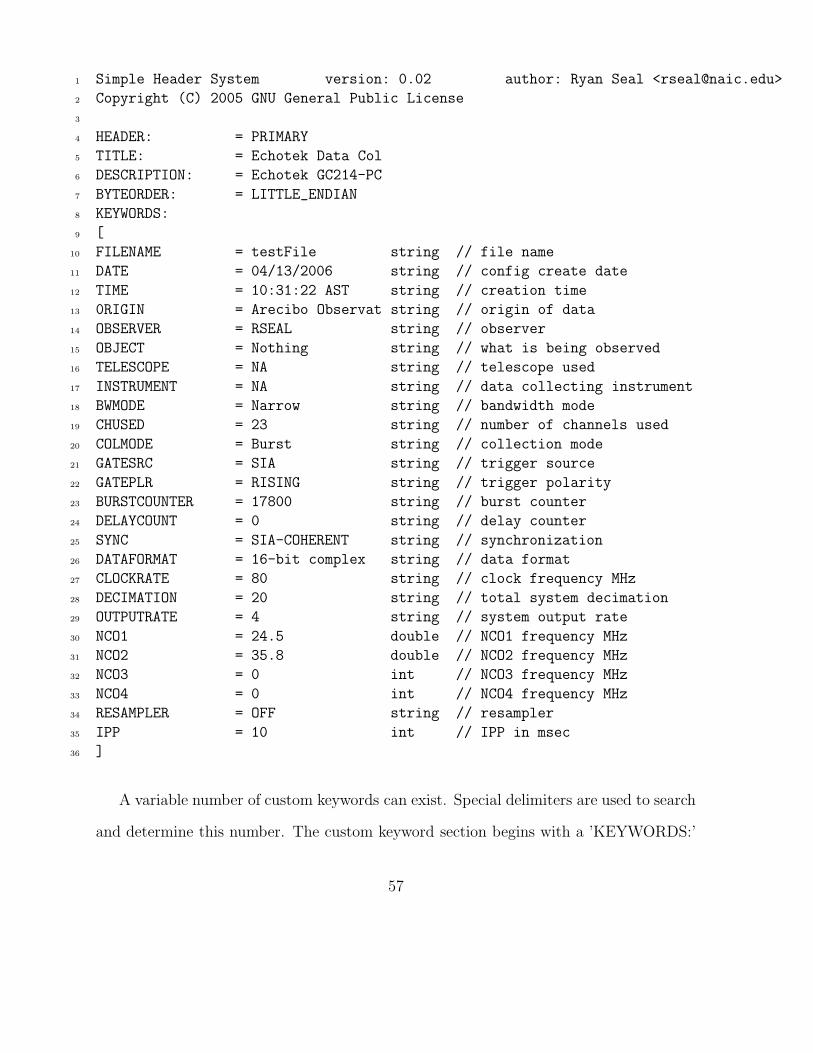
1 Simple Header System version: 0.02 author: Ryan Seal <[email protected]>
2 Copyright (C) 2005 GNU General Public License
3
4 HEADER: = PRIMARY
5 TITLE: = Echotek Data Col
6 DESCRIPTION: = Echotek GC214-PC
7 BYTEORDER: = LITTLE_ENDIAN
8 KEYWORDS:
9 [
10 FILENAME = testFile string // file name
11 DATE = 04/13/2006 string // config create date
12 TIME = 10:31:22 AST string // creation time
13 0RIGIN = Arecibo Observat string // origin of data
14 OBSERVER = RSEAL string // observer
15 OBJECT = Nothing string // what is being observed
16 TELESCOPE = NA string // telescope used
17 INSTRUMENT = NA string // data collecting instrument
18 BWMODE = Narrow string // bandwidth mode
19 CHUSED = 23 string // number of channels used
20 COLMODE = Burst string // collection mode
21 GATESRC = SIA string // trigger source
22 GATEPLR = RISING string // trigger polarity
23 BURSTCOUNTER = 17800 string // burst counter
24 DELAYCOUNT = 0 string // delay counter
25 SYNC = SIA-COHERENT string // synchronization
26 DATAFORMAT = 16-bit complex string // data format
27 CLOCKRATE = 80 string // clock frequency MHz
28 DECIMATION = 20 string // total system decimation
29 OUTPUTRATE = 4 string // system output rate
30 NCO1 = 24.5 double // NCO1 frequency MHz
31 NCO2 = 35.8 double // NCO2 frequency MHz
32 NCO3 = 0 int // NCO3 frequency MHz
33 NCO4 = 0 int // NCO4 frequency MHz
34 RESAMPLER = OFF string // resampler
35 IPP = 10 int // IPP in msec
36 ]
A variable number of custom keywords can exist. Special delimiters are used to search
and determine this number. The custom keyword section begins with a ’KEYWORDS:’
57
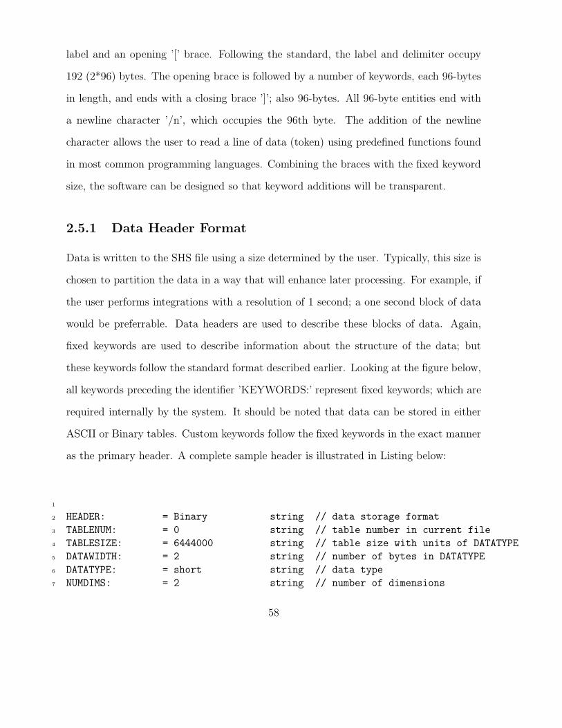
label and an opening ’[’ brace. Following the standard, the label and delimiter occupy
192 (2*96) bytes. The opening brace is followed by a number of keywords, each 96-bytes
in length, and ends with a closing brace ’]’; also 96-bytes. All 96-byte entities end with
a newline character ’/n’, which occupies the 96th byte. The addition of the newline
character allows the user to read a line of data (token) using predefined functions found
in most common programming languages. Combining the braces with the fixed keyword
size, the software can be designed so that keyword additions will be transparent.
2.5.1 Data Header Format
Data is written to the SHS file using a size determined by the user. Typically, this size is
chosen to partition the data in a way that will enhance later processing. For example, if
the user performs integrations with a resolution of 1 second; a one second block of data
would be preferrable. Data headers are used to describe these blocks of data. Again,
fixed keywords are used to describe information about the structure of the data; but
these keywords follow the standard format described earlier. Looking at the figure below,
all keywords preceding the identifier ’KEYWORDS:’ represent fixed keywords; which are
required internally by the system. It should be noted that data can be stored in either
ASCII or Binary tables. Custom keywords follow the fixed keywords in the exact manner
as the primary header. A complete sample header is illustrated in Listing below:
1
2 HEADER: = Binary string // data storage format
3 TABLENUM: = 0 string // table number in current file
4 TABLESIZE: = 6444000 string // table size with units of DATATYPE
5 DATAWIDTH: = 2 string // number of bytes in DATATYPE
6 DATATYPE: = short string // data type
7 NUMDIMS: = 2 string // number of dimensions
58
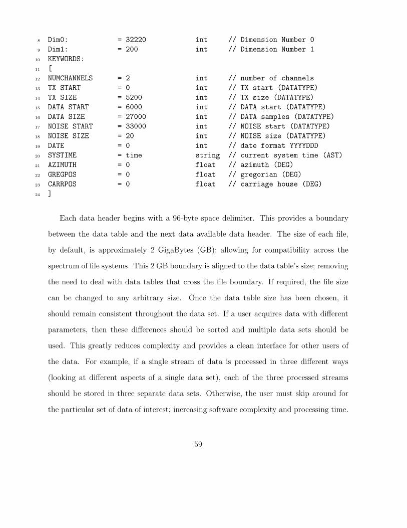
8 Dim0: = 32220 int // Dimension Number 0
9 Dim1: = 200 int // Dimension Number 1
10 KEYWORDS:
11 [
12 NUMCHANNELS = 2 int // number of channels
13 TX START = 0 int // TX start (DATATYPE)
14 TX SIZE = 5200 int // TX size (DATATYPE)
15 DATA START = 6000 int // DATA start (DATATYPE)
16 DATA SIZE = 27000 int // DATA samples (DATATYPE)
17 NOISE START = 33000 int // NOISE start (DATATYPE)
18 NOISE SIZE = 20 int // NOISE size (DATATYPE)
19 DATE = 0 int // date format YYYYDDD
20 SYSTIME = time string // current system time (AST)
21 AZIMUTH = 0 float // azimuth (DEG)
22 GREGPOS = 0 float // gregorian (DEG)
23 CARRPOS = 0 float // carriage house (DEG)
24 ]
Each data header begins with a 96-byte space delimiter. This provides a boundary
between the data table and the next data available data header. The size of each file,
by default, is approximately 2 GigaBytes (GB); allowing for compatibility across the
spectrum of file systems. This 2 GB boundary is aligned to the data table’s size; removing
the need to deal with data tables that cross the file boundary. If required, the file size
can be changed to any arbitrary size. Once the data table size has been chosen, it
should remain consistent throughout the data set. If a user acquires data with different
parameters, then these differences should be sorted and multiple data sets should be
used. This greatly reduces complexity and provides a clean interface for other users of
the data. For example, if a single stream of data is processed in three different ways
(looking at different aspects of a single data set), each of the three processed streams
should be stored in three separate data sets. Otherwise, the user must skip around for
the particular set of data of interest; increasing software complexity and processing time.
59
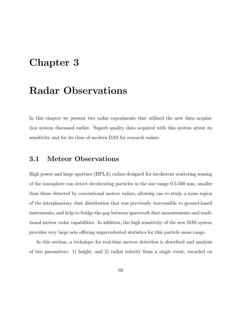
Chapter 3
Radar Observations
In this chapter we present two radar experiments that utilized the new data acquisi-
tion system discussed earlier. Superb quality data acquired with this system attest its
sensitivity and for its class of modern DAS for research radars.
3.1 Meteor Observations
High power and large aperture (HPLA) radars designed for incoherent scattering sensing
of the ionosphere can detect decelerating particles in the size range 0.5-500 mm, smaller
than those detected by conventional meteor radars, allowing one to study a mass region
of the interplanetary dust distribution that was previously inaccessible to ground-based
instruments, and help to bridge the gap between spacecraft dust measurements and tradi-
tional meteor radar capabilities. In addition, the high sensitivity of the new DAS system
provides very large sets offering unprecedented statistics for this particle mass range.
In this section, a technique for real-time meteor detection is described and analysis
of two parameters: 1) height, and 2) radial velocity from a single event, recorded on
60
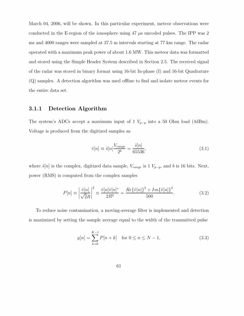
March 04, 2006, will be shown. In this particular experiment, meteor observations were
conducted in the E-region of the ionosphere using 47 µs uncoded pulses. The IPP was 2
ms and 4000 ranges were sampled at 37.5 m intervals starting at 77 km range. The radar
operated with a maximum peak power of about 1.6 MW. This meteor data was formatted
and stored using the Simple Header System described in Section 2.5. The received signal
of the radar was stored in binary format using 16-bit In-phase (I) and 16-bit Quadrature
(Q) samples. A detection algorithm was used offline to find and isolate meteor events for
the entire data set.
3.1.1 Detection Algorithm
The system’s ADCs accept a maximum input of 1 Vp−p into a 50 Ohm load (4dBm).
Voltage is produced from the digitized samples as
v[n] ≡ s[n]Vrange
2b=
s[n]
65536, (3.1)
where s[n] is the complex, digitized data sample, Vrange is 1 Vp−p, and b is 16 bits. Next,
power (RMS) is computed from the complex samples
P [n] ≡∣
∣
∣
∣
v[n]√2R
∣
∣
∣
∣
2
≡ v[n]v[n]∗
2R2=
Rev[n]2 + Imv[n]2
500. (3.2)
To reduce noise contamination, a moving-average filter is implemented and detection
is maximized by setting the sample average equal to the width of the transmitted pulse
y[n] =K−1∑
k=0
P [n + k] for 0 ≤ n ≤ N − 1, (3.3)
61

where K is the length of the transmitted pulse and N is the total number of samples.
This operation is essentially a cross-correlation of the received signal with the normalized
transmitter pulse. For efficiency, the filter is implemented recursively beginnning with
computation of the initial value
y[0] =
K−1∑
k=0
P [k].
Remaining computations are reduced to
y[n] = y[n − 1] + P [n + K] − P [n − 1] for 1 ≤ n ≤ N − 1.
Next, a fast-time (1 IPP) noise estimate is determined by
Pn =1
N − M
N−1∑
n=M
P [n], (3.4)
where M is the starting height and N is the final height used in the estimation. The
filtered signal and a scaled noise estimate are used to determine detection
y[n] > αPn, (3.5)
where α is the threshhold value. This process is repeated for each IPP.
3.1.2 Parameter Estimation
To verify system operation, a number of events were recorded simultaneously with the
current system. Two parameters, height and velocity, were processed using the new DAS
and verified with the current system. In this section, a discussion of the method used for
processing will be given using a single event detected on March 04, 2006.
62
Each table of data stored using the SHS file system contains one second of data. Using
an IPP of 2 ms, 500 IPPs are available per table. The Range Time Intensity (RTI) plot
displays range and IPP number in the x-y directions and power is displayed using a color
map. Figure 3.1 illustrates an RTI plot of an event at 4:10:01 AST. From the image in
Figure 3.1: Range Time Intensity (RTI) plot
Figure 3.1, a single IPP is isolated from the data and plotted in Figure 3.2. This figure
provides enough information to compute both range and velocity of the meteor. In this
example, steps taken to process this information are automated using MATLAB software
and details are located in B.1. First, power from the radar return is computed for a single
IPP and is illustrated in Figure 3.3. Second, a cross-correlation of the power signal with
63
power from the transmitted pulse are computed. The result will produce a waveform as
shown in Figure 3.4. The peak of this waveform provides the midpoint of the meteor’s
range and is used to isolate the event for further processing. Isolation of the detected
event is shown in Figure 3.5. Next, an FFT analysis is performed on the isolated event
and the results are normalized as shown in Figure 3.6. The spectrm’s peak is used to
calculate the meteor’s radial velocity using
v = fd
λ
2, (3.6)
where v represents radial velocity (m/s), fd is the spectrum peak, and λ is the wavelength
of the transmitted carrier (m). The following results were processed and verified with the
current system:
1. Range: 97.039 km ± 18.74 m
60 80 100 120 140 160 180 200 220 240−600
−400
−200
0
200
400
600
Altitude (Km)
Vol
ts (
V)
Meteor Detection − Time Domain
Figure 3.2: IPP illustrating meteor in time domain
64
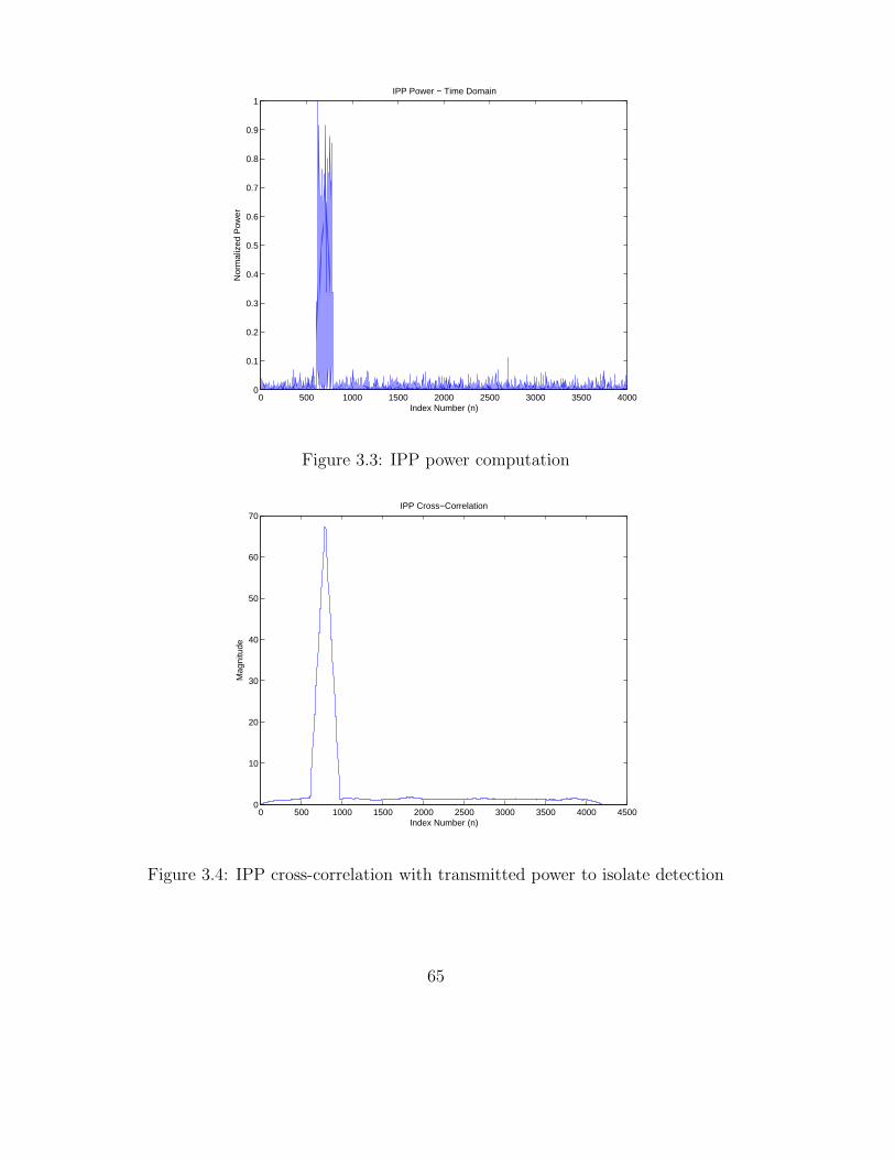
0 500 1000 1500 2000 2500 3000 3500 40000
0.1
0.2
0.3
0.4
0.5
0.6
0.7
0.8
0.9
1
Index Number (n)
Nor
mal
ized
Pow
er
IPP Power − Time Domain
Figure 3.3: IPP power computation
0 500 1000 1500 2000 2500 3000 3500 4000 45000
10
20
30
40
50
60
70
Index Number (n)
Mag
nitu
de
IPP Cross−Correlation
Figure 3.4: IPP cross-correlation with transmitted power to isolate detection
65
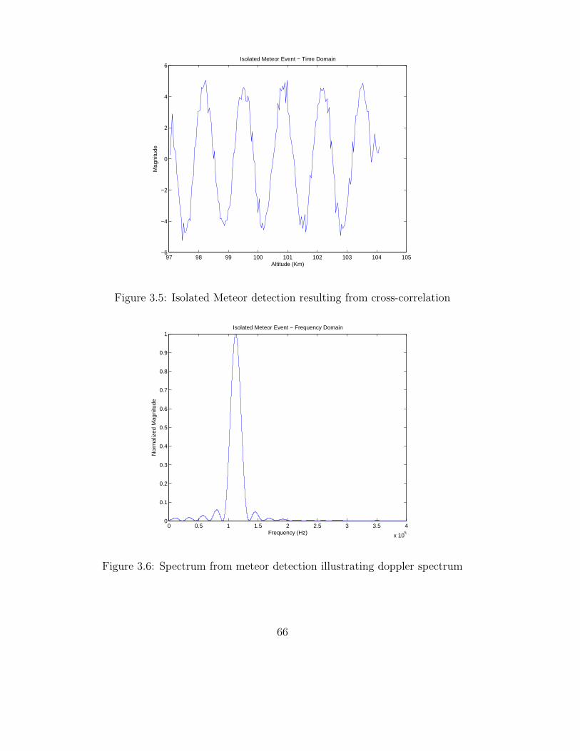
97 98 99 100 101 102 103 104 105−6
−4
−2
0
2
4
6
Altitude (Km)
Mag
nitu
de
Isolated Meteor Event − Time Domain
Figure 3.5: Isolated Meteor detection resulting from cross-correlation
0 0.5 1 1.5 2 2.5 3 3.5 4
x 105
0
0.1
0.2
0.3
0.4
0.5
0.6
0.7
0.8
0.9
1
Frequency (Hz)
Nor
mal
ized
Mag
nitu
de
Isolated Meteor Event − Frequency Domain
Figure 3.6: Spectrum from meteor detection illustrating doppler spectrum
66
2. Velocity: 39.219 km/s ± 61.04 m/s
Error estimation of range was based on the system’s sampling rate (4 MHz) and velocity
error was calculated using both sampling rate and the number of points (32k) used in the
FFT analysis. Events from the current system were processed and a comparison revealed
precise matching, thus verifying system operation.
3.2 Plasma Line Observations
It is well-known that the most accurate method for measuring the electron density in the
upper atmosphere is using the plasma line resonance, which occurs close to the plasma
line frequency as predicted by incoherent scatter (IS) theory [e.g., Dougherty and Farley,
1960; Salpeter , 1960]. The plasma line (caused by scattering from electron plasma
waves) is greatly enhanced over thermal levels during the daytime by photo electrons
[e.g., Yngvesson and Perkins, 1968]. The information in the plasma line resonance lies
in the frequency of the return, not in the shape of the spectrum, as is the case for the
ion line. Frequency measurements are much more accurate than power or amplitude
measurements since they do not depend on receiver gains and system losses, which are
often difficult to measure and quite variable. Thus, using the plasma line resonance
frequency as an ionospheric diagnostic is particularly useful.
In this section, we present the first results of a new technique for measuring the
electron temperature in the daytime ionosphere using the Arecibo incoherent scatter
radar (ISR). The technique utilizes the plasma line component of the incoherent scatter
spectrum. The difference in the up- and down-shifted plasma line frequencies is related
to the density and temperature of the ionosphere, as well as more minor effects resulting
from photoelectrons, currents, and other sources. The shift is very small (the order of
67

1 kHz in a plasma line frequency of several MHz) but can be measured quite accurately
with the coded long pulse plasma line technique. We compare the results to ion line
measurements of the electron temperature, and the two in dependent techniques show
good agreement. In addition to providing a measure of the electron temperature that
is independent of the ion line, the approach allows for a sensitive test of kinetic plasma
theory including a magnetic field, gives us the ability to study photoelectron populations
and electron currents, and will allow us to constrain ion line fits in the bottomside (and
possibly topside) regions to more accurately fit for composition.
68
Chapter 4
Conclusions and Future Work
It is clear that the new DAS for the Arecibo radar has the capability of measuring high
quality data as attested by both meteor and plasma radar observations. The flexibility
and reliability of the system allows visiting scientists to develop exciting experiments in
space science.
We plan to enhance data throughput, system flexibility and capabilities by including
Field Programmable Gate Arrays (FPGA) technology at the front-end of the data acqui-
sition system and utilized a USB port for system control and communication. Of course
segments of the software presented in this thesis will have to be modified and adapted in
order to integrate this FPGA system. Also, the integration of a radar controller with the
data acquisition system will be conducted.
Finally, the radar software and control programs developed under this project will be
available freely to anybody through the Open Source software development web site of
SourceForge at: [ http://sourceforge.net].
69
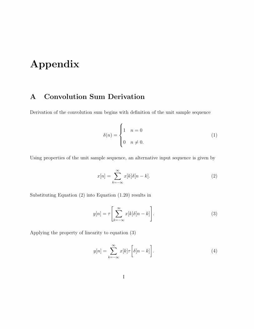
Appendix
A Convolution Sum Derivation
Derivation of the convolution sum begins with definition of the unit sample sequence
δ(n) =
1 n = 0
0 n 6= 0.
(1)
Using properties of the unit sample sequence, an alternative input sequence is given by
x[n] =∞
∑
k=−∞
x[k]δ[n − k]. (2)
Substituting Equation (2) into Equation (1.20) results in
y[n] = τ
[
∞∑
k=−∞
x[k]δ[n − k]
]
. (3)
Applying the property of linearity to equation (3)
y[n] =
∞∑
k=−∞
x[k]τ
[
δ[n − k]
]
. (4)
I
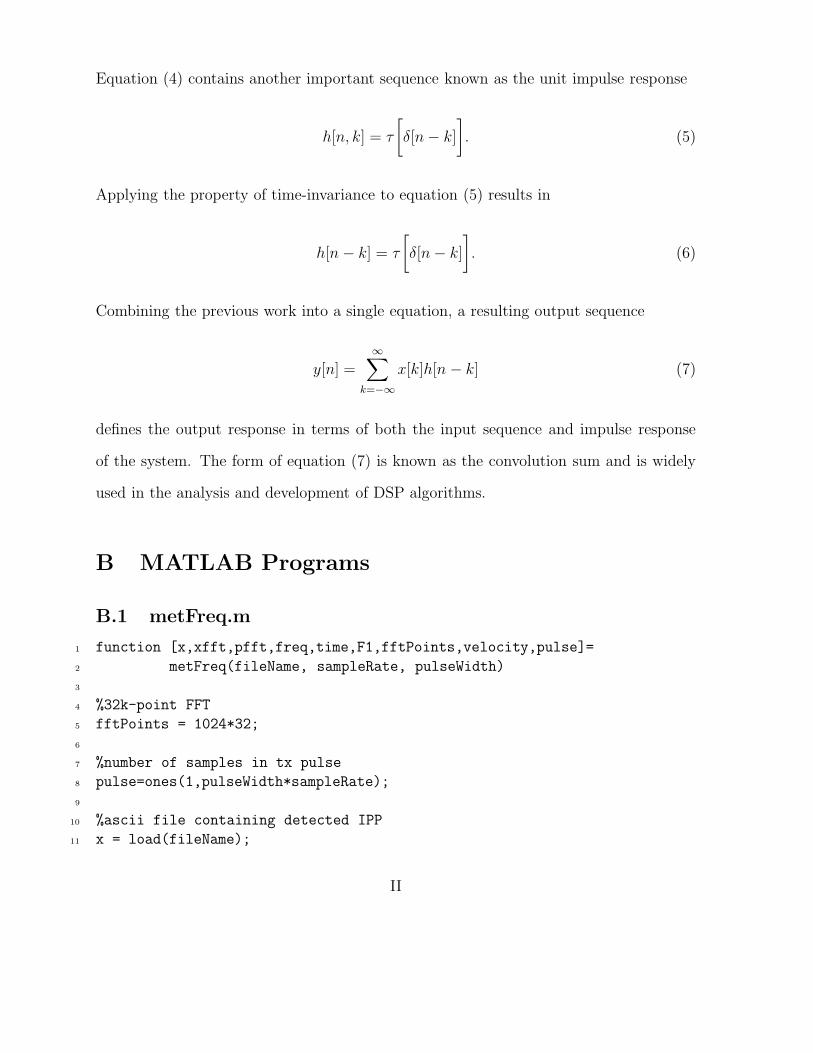
Equation (4) contains another important sequence known as the unit impulse response
h[n, k] = τ
[
δ[n − k]
]
. (5)
Applying the property of time-invariance to equation (5) results in
h[n − k] = τ
[
δ[n − k]
]
. (6)
Combining the previous work into a single equation, a resulting output sequence
y[n] =∞
∑
k=−∞
x[k]h[n − k] (7)
defines the output response in terms of both the input sequence and impulse response
of the system. The form of equation (7) is known as the convolution sum and is widely
used in the analysis and development of DSP algorithms.
B MATLAB Programs
B.1 metFreq.m
1 function [x,xfft,pfft,freq,time,F1,fftPoints,velocity,pulse]=
2 metFreq(fileName, sampleRate, pulseWidth)
3
4 %32k-point FFT
5 fftPoints = 1024*32;
6
7 %number of samples in tx pulse
8 pulse=ones(1,pulseWidth*sampleRate);
9
10 %ascii file containing detected IPP
11 x = load(fileName);
II
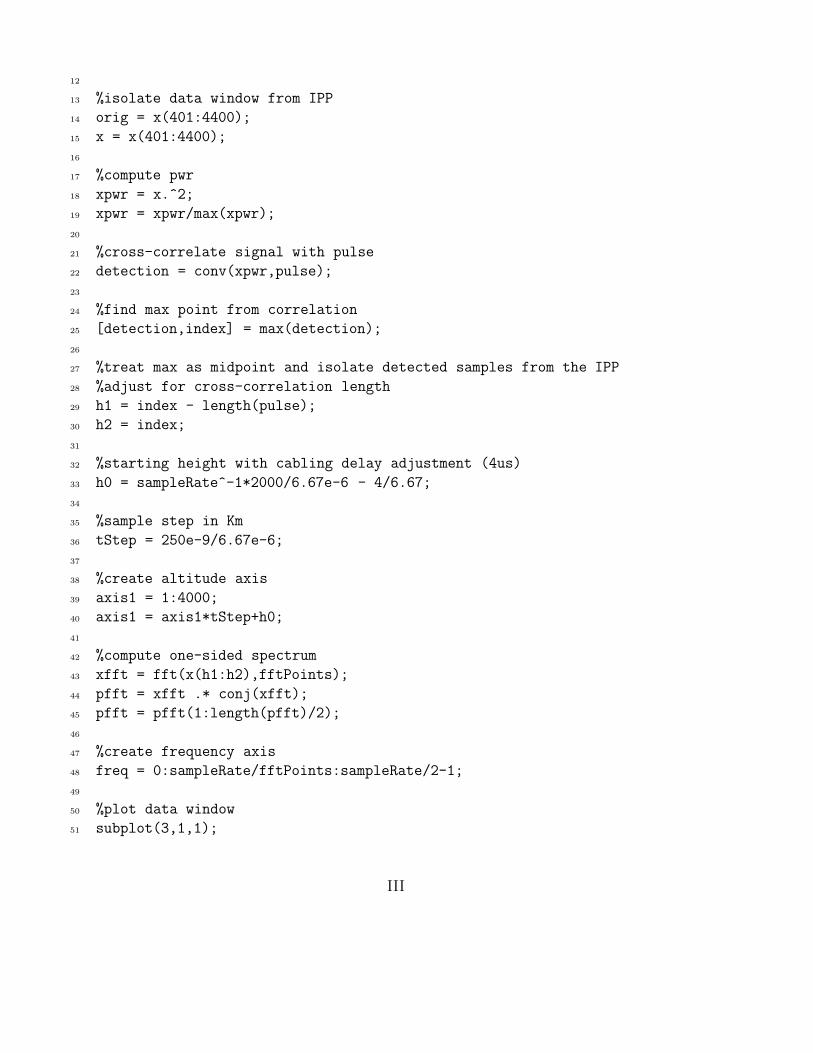
12
13 %isolate data window from IPP
14 orig = x(401:4400);
15 x = x(401:4400);
16
17 %compute pwr
18 xpwr = x.^2;
19 xpwr = xpwr/max(xpwr);
20
21 %cross-correlate signal with pulse
22 detection = conv(xpwr,pulse);
23
24 %find max point from correlation
25 [detection,index] = max(detection);
26
27 %treat max as midpoint and isolate detected samples from the IPP
28 %adjust for cross-correlation length
29 h1 = index - length(pulse);
30 h2 = index;
31
32 %starting height with cabling delay adjustment (4us)
33 h0 = sampleRate^-1*2000/6.67e-6 - 4/6.67;
34
35 %sample step in Km
36 tStep = 250e-9/6.67e-6;
37
38 %create altitude axis
39 axis1 = 1:4000;
40 axis1 = axis1*tStep+h0;
41
42 %compute one-sided spectrum
43 xfft = fft(x(h1:h2),fftPoints);
44 pfft = xfft .* conj(xfft);
45 pfft = pfft(1:length(pfft)/2);
46
47 %create frequency axis
48 freq = 0:sampleRate/fftPoints:sampleRate/2-1;
49
50 %plot data window
51 subplot(3,1,1);
III

52 plot(axis1,orig);
53
54 %plot detection window
55 subplot(3,1,2);
56 plot(axis1(h1:h2),x(h1:h2));
57
58 %plot normalized spectrum
59 subplot(3,1,3);
60 pfft = pfft / max(pfft);
61 plot(freq,pfft);
62
63 %search for spectrum max
64 for i=1:length(pfft)
65 if(pfft(i)==1) maxPoint = i;
66 end
67 end
68
69 %compute radial velocity from doppler spectrum
70 velocity = (freq(maxPoint)/2)*(3e8/430e6)
71 hDetect = axis1(h1)
72 error = sampleRate/fftPoints
73 %\endlstlisting
IV
Bibliography
[1] A technical report on digital signal synthesis. Technical report, Analog Devices,
1999.
[2] Automatic I/O Scheduler Selection for Latency and Bandwidth Optimization, 2005.
[3] A. Binstock. The producer/consumer threading model.
[4] G. Booch. Object Oriented Analysis and Design with Applications. The Benjam-
in/Cummings Publishing Company, Inc., 1994.
[5] C. Cantrell. Modern Mathematical Methods for Physicists and Engineers. Cambridge
University Press, 2000.
[6] M. Fowler. UML Distilled Third Edition. Pearson Education, Inc., 2004.
[7] F. J. Harris. Multirate Signal Processing for Communication Systems. Prentice Hall
Professional Technical Reference, 2005.
[8] E. B. Hogenaeur. An economic class of digital filters for decimation and interpolation.
IEEE transactions on Acoustics, Speech, and Signal Processing, ASSP-29(2), April
1981.
V
[9] B. Izouggaghen, A. Khouas, and Y. Savaria. Spurs modeling in direct digital period
synthesizers related to phase accumulator truncation. Internation Symposium on
Circuits and Systems, 2004.
[10] E. Kudeki. Applications of radiowave propagation. 2003.
[11] G. Miller. The magical number seven, plus or minus two: Some limits on our capacity
for processing information. The Psychological Review, 63(2), 1956.
[12] K. Morris. Death of the hardware engineer. Embedded Technology Journal, 2006.
[13] A. V. Oppenheim and R. W. Schafer. Digital Signal Processing. Prentice-Hall Inc.,
1975.
[14] P. E. Pace. Advanced Techniques for Digital Receivers. Artech House, 2000.
[15] J. G. Proadkis and D. G. Manolikis. Digital Signal Processing Principles, Algorithms,
and Applications. Prentice-Hall, Inc., 1996.
[16] D. Robbins. Common threads: Advanced filesystem implementor’s guide, part 3,
2001.
[17] B. C. Rorabaugh. DSP Primer. The McGraw-Hill companies, 1999.
[18] K. M. Sanjit. Digital Signal Processing: A Computer Based Approach. McGraw-Hill
Companies, Inc., 2006.
[19] A. Shalloway and J. R. Trott. Design Patterns Explained: A New Perspective on
Object Oriented Design. Addison-Wesley Pearson Education, Inc., 2005.
[20] C. E. Shannon. Communication in the presence of noise. volume 86. Proceedings of
the IEEE, February 1998.
VI
[21] Texas Instruments. GC4016 MULTI-STANDARD QUAD DDC CHIP DATA
SHEET, 1.0 edition, August 27 2001.
[22] A. Torosyan and A. N. W. Jr. Analysis of the output spectrum of direct digi-
tal frequency synthesizers in the presence of phase truncation and finite arithmetic
precision. International Symposium for Image and Signal Processing and Analysis,
2001.
[23] J. B.-Y. Tsui. Digital Techniques for Wideband Receivers. Artech House, May 2001.
[24] R. G. Vaughan. The theory of bandpass sampling. IEEE Transactions on Signal
Processing, 39, 1991.
VII
Related Documents