MUFFAKHAM JAH COLLEGE OF ENGINEERING AND TECHNOLOGY EC-291 ELECTRONIC ENGINEERING - II LAB (For EEE & EIE) (With effect from the academic year 2015-2016) STUDENT’S MANUAL DEPARTMENT OF ELECTRONICS AND COMMUNICATION ENGINEERING

Welcome message from author
This document is posted to help you gain knowledge. Please leave a comment to let me know what you think about it! Share it to your friends and learn new things together.
Transcript
MUFFAKHAM JAH
COLLEGE OF ENGINEERING AND TECHNOLOGY
EC-291 ELECTRONIC ENGINEERING - II LAB
(For EEE & EIE)
(With effect from the academic year 2015-2016)
STUDENT’S MANUAL
DEPARTMENT OF
ELECTRONICS AND COMMUNICATION ENGINEERING

Electronic Engineering-II Lab E.C.E. Department
MJCET Page 2
Vision and Mission of the Institution
Vision
To be part of universal human quest for development and progress by contributing high calibre,
ethical and socially responsible engineers who meet the global challenge of building modern
society in harmony with nature.
Mission
• To attain excellence in imparting technical education from the undergraduate through
doctorate levels by adopting coherent and judiciously coordinated curricular and co-curricular
programs
• To foster partnership with industry and government agencies through collaborative research
and consultancy
• To nurture and strengthen auxiliary soft skills for overall development and improved
employability in a multi-cultural work space
• To develop scientific temper and spirit of enquiry in order to harness the latent innovative
talents
• To develop constructive attitude in students towards the task of nation building and empower
them to become future leaders
• To nourish the entrepreneurial instincts of the students and hone their business acumen.
• To involve the students and the faculty in solving local community problems through
economical and sustainable solutions.
Vision and Mission of ECE Department
Vision
To be recognized as a premier education center providing state of art education and facilitating
research and innovation in the field of Electronics and Communication.
Mission
We are dedicated to providing high quality, holistic education in Electronics and Communication
Engineering that prepares the students for successful pursuit of higher education and challenging
careers in research, R& D and Academics.
Program Educational Objectives of B. E (ECE) Program:
1. Graduates will demonstrate technical competence in their chosen fields of employment by
identifying, formulating, analyzing and providing engineering solutions using current
techniques and tools
2. Graduates will communicate effectively as individuals or team members and demonstrate
leadership skills to be successful in the local and global cross-cultural working environment
3. Graduates will demonstrate lifelong learning through continuing education and professional
development
4. Graduates will be successful in providing viable and sustainable solutions within societal,
professional, environmental and ethical contexts

Electronic Engineering-II Lab E.C.E. Department
MJCET Page 3
MUFFAKHAM JAH COLLEGE OF ENGINEERING AND TECHNOLOGY
BANJARA HILLS, ROAD NO-3, TELANGANA
LABORATORY MANUAL
FOR
ELECTRONIC ENGINEERING -II LAB
Prepared by: Checked by:
Approved by:
Electronic Engineering-II Lab E.C.E. Department
MJCET Page 4
MUFFAKHAM JAH COLLEGE OF ENGINEERING AND TECHNOLOGY
DEPARTMENT OF ELECTRONICS AND COMMUNICATIONS ENGINEERING
(Name of the Subject/Lab Course): ELECTRONIC ENGINEREERING-II LAB
Code: EC291 Programme: UG
Branch: ECE Version No: 1
Year : II Updated on: 20/3/16
Semester :II No. of Pages:
Classification Status(Unrestricted/restricted): Unrestricted
Distribution List :Department, Lab, Library, Lab Incharge
Prepared by: 1) Name : 1) Name :
2) Sign : 2) Sign :
3)Designation : 3) Designation :
4) Date : 4) Date :
Verified by: 1) Name : * For Q.C Only
2) Sign : 1) Name :
3)Designation : 2) Sign :
4) Date : 3) Designation :
4) Date :
Approved by: (HOD) 1) Name:
2) Sign :
3) Date :
Electronic Engineering-II Lab E.C.E. Department
MJCET Page 5
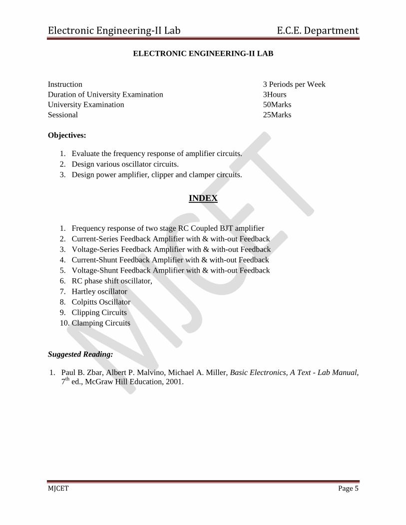
ELECTRONIC ENGINEERING-II LAB
Instruction 3 Periods per Week
Duration of University Examination 3Hours
University Examination 50Marks
Sessional 25Marks
Objectives:
1. Evaluate the frequency response of amplifier circuits.
2. Design various oscillator circuits.
3. Design power amplifier, clipper and clamper circuits.
INDEX
1. Frequency response of two stage RC Coupled BJT amplifier
2. Current-Series Feedback Amplifier with & with-out Feedback
3. Voltage-Series Feedback Amplifier with & with-out Feedback
4. Current-Shunt Feedback Amplifier with & with-out Feedback
5. Voltage-Shunt Feedback Amplifier with & with-out Feedback
6. RC phase shift oscillator,
7. Hartley oscillator
8. Colpitts Oscillator
9. Clipping Circuits
10. Clamping Circuits
Suggested Reading:
1. Paul B. Zbar, Albert P. Malvino, Michael A. Miller, Basic Electronics, A Text - Lab Manual,
7th
ed., McGraw Hill Education, 2001.

Electronic Engineering-II Lab E.C.E. Department
MJCET Page 6
ELECTRONICS ENGINEERING-II LAB
GENERAL GUIDELINES AND SAFETY INSTRUCTIONS
1. Sign in the log register as soon as you enter the lab and strictly observe your lab timings.
2. Strictly follow the written and verbal instructions given by the teacher / Lab Instructor. If
you do not understand the instructions, the handouts and the procedures, ask the
instructor or teacher.
3. Never work alone! You should be accompanied by your laboratory partner and / or the
instructors / teaching assistants all the time.
4. It is mandatory to come to lab in a formal dress and wear your ID cards.
5. Do not wear loose-fitting clothing or jewellery in the lab. Rings and necklaces are usual
excellent conductors of electricity.
6. Mobile phones should be switched off in the lab. Keep bags in the bag rack.
7. Keep the labs clean at all times, no food and drinks allowed inside the lab.
8. Intentional misconduct will lead to expulsion from the lab.
9. Do not handle any equipment without reading the safety instructions. Read the handout
and procedures in the Lab Manual before starting the experiments.
10. Do your wiring, setup, and a careful circuit checkout before applying power. Do not
make circuit changes or perform any wiring when power is on.
11. Avoid contact with energized electrical circuits.
12. Do not insert connectors forcefully into the sockets.
13. NEVER try to experiment with the power from the wall plug.
14. Immediately report dangerous or exceptional conditions to the Lab instructor / teacher:
Equipment that is not working as expected, wires or connectors are broken, the
equipment that smells or “smokes”. If you are not sure what the problem is or what's
going on, switch off the Emergency shutdown.
15. Never use damaged instruments, wires or connectors. Hand over these parts to the Lab
instructor/Teacher.
16. Be sure of location of fire extinguishers and first aid kits in the laboratory.
17. After completion of Experiment, return the bread board, trainer kits, wires, CRO probes
and other components to lab staff. Do not take any item from the lab without permission.
18. Observation book and lab record should be carried to each lab. Readings of current lab
experiment are to be entered in Observation book and previous lab experiment should be
written in Lab record book. Both the books should be corrected by the faculty in each lab.
19. Handling of Semiconductor Components:Sensitive electronic circuits and electronic
components have to be handled with great care. The inappropriate handling of electronic
component can damage or destroy the devices. The devices can be destroyed by driving
to high currents through the device, by overheating the device, by mixing up the polarity,
or by electrostatic discharge (ESD). Therefore, always handle the electronic devices as
indicated by the handout, the specifications in the data sheet or other documentation.
20. Special Precautions during soldering practice
a. Hold the soldering iron away from your body. Don't point the iron towards you.
b. Don't use a spread solder on the board as it may cause short circuit.
c. Do not overheat the components as excess heat may damage the components/board.
d. In case of burn or injury seek first aid available in the lab or at the college dispensary

Electronic Engineering-II Lab E.C.E. Department
MJCET Page 7
List of Experiments Page #
1. Frequency response of two stage RC Coupled BJT amplifier 8
2. Current-Series Feedback Amplifier with & with-out Feedback 12
3. Voltage-Series Feedback Amplifier with & with-out Feedback 15
4. Current-Shunt Feedback Amplifier with & with-out Feedback 19
5. Voltage-Shunt Feedback Amplifier with & with-out Feedback 23
6. RC phase shift oscillator, 26
7. Hartley oscillator 30
8. Colpitts Oscillator 33
9. Clipping Circuits 37
10. Clamping Circuits 40
11. Appendix 44
Electronic Engineering-II Lab E.C.E. Department
MJCET Page 8
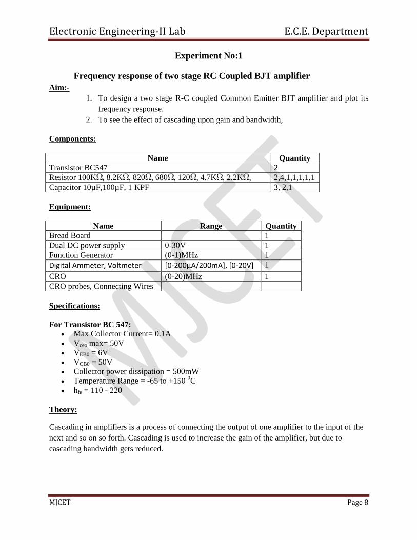
Experiment No:1
Frequency response of two stage RC Coupled BJT amplifier
Aim:-
1. To design a two stage R-C coupled Common Emitter BJT amplifier and plot its
frequency response.
2. To see the effect of cascading upon gain and bandwidth,
Components:
Name Quantity
Transistor BC547 2
Resistor 100K , 8.2K , 820 , 680 , 120 , 4.7K , 2.2K , 2,4,1,1,1,1,1
Capacitor 10µF,100µF, 1 KPF 3, 2,1
Equipment:
Name Range Quantity
Bread Board 1
Dual DC power supply 0-30V 1
Function Generator (0-1)MHz 1
Digital Ammeter, Voltmeter [0-200µA/200mA], [0-20V] 1
CRO (0-20)MHz 1
CRO probes, Connecting Wires
Specifications:
For Transistor BC 547:
Max Collector Current= 0.1A
Vceo max= 50V
VEB0 = 6V
VCB0 = 50V
Collector power dissipation = 500mW
Temperature Range = -65 to +150 0C
hfe = 110 - 220
Theory:
Cascading in amplifiers is a process of connecting the output of one amplifier to the input of the
next and so on so forth. Cascading is used to increase the gain of the amplifier, but due to
cascading bandwidth gets reduced.

Electronic Engineering-II Lab E.C.E. Department
MJCET Page 9
In a multistage amplifier the overall voltage gain is the product of individual voltage gains. But
the bandwidth of a multistage amplifier is always smaller than the bandwidth of individual
stages.
Circuit diagram:
Procedure:
1) Connect the circuit as shown in figure1.
2) Note the DC conditions i.e, the values of base, collector currents and base to emitter,
collector to emitter voltages for each stage.
3) Connect the circuit as shown in figure 2, Adjust the input signal frequency to 1 KHz and
the peak to peak value of Vi1 to 2 or 3mV. Note the peak to peak value of output voltage
Vo1 and Vo2. Calculate the voltage gain of each stage.
For stage-1, 1
1
1
i
O
VV
VA
For stage-2, 1
2
2
O
O
VV
VA
And overall voltage gain is, 21 VVV AAA
4) Vary the frequency of the input signal from 30 Hz to 500 KHz in appropriate steps,
maintain the Vi1 constant at 2mV and note the output voltages in each step.
5) Calculate the gains AV1, AV2, and AV for each value of frequency. Plot a graph between
gain and frequency for each stage and the overall stage
6) Calculate bandwidth of each stage and the overall stage from the graph.
Electronic Engineering-II Lab E.C.E. Department
MJCET Page 10
Observations:
DC conditions:
For stage-1, VBE1 = ……………. VCE1 = ………………
IB1 = ……………… IC1 = ………………..
For stage-2, VBE2 = ……………. VCE2 = ………………
IB2 = ……………… IC2 = ………………..
Frequency Response:
Sl.No. Frequency Vi1
(mV)
VO1
(mV)
VO2 (V)
1
1
1
i
O
VV
VA
1
2
2
O
O
VV
VA
21 VVV AAA
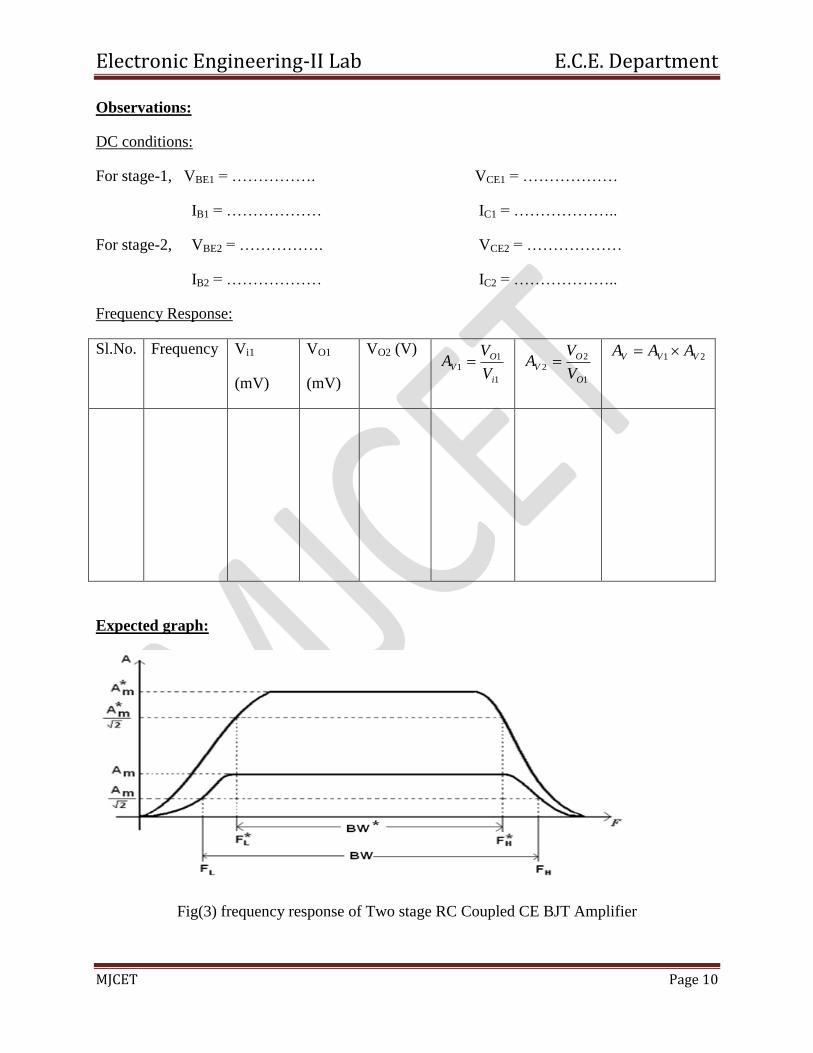
Expected graph:
Fig(3) frequency response of Two stage RC Coupled CE BJT Amplifier
Electronic Engineering-II Lab E.C.E. Department
MJCET Page 11
Result:
1) The frequency response of individual and overall stages is plotted.
2) Mid frequency gains are,
AVm1 = ……………. AVm2 = …………… AVm = ………………
3) Bandwidths are,
BW1 = …………… BW2 = ………….. BW = …………..
4) It is observed that cascading in amplifiers increases the voltage gain but decreases the
bandwidth.

Electronic Engineering-II Lab E.C.E. Department
MJCET Page 12
Experiment No: 2
Current series Feedback Amplifier
Aim: To find the Bandwidth of Current series feedback amplifier without and with feedback.
Apparatus: Dc power supply, Multimeter, Resistors 1kΩ ,33 kΩ,4.7 kΩ(2),5.6 kΩ(2),
BJT(BC548), Bread Board, Function generator, Connecting wires, Electrolytic capacitors
10µF(2),100 µF, Ceramic capacitor 1kpf(2).
Circuit Diagram
Electronic Engineering-II Lab E.C.E. Department
MJCET Page 13
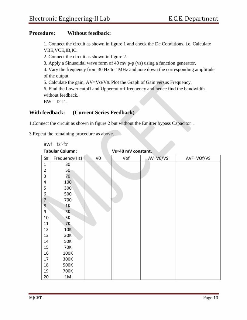
Procedure: Without feedback:
1. Connect the circuit as shown in figure 1 and check the Dc Conditions. i.e. Calculate
VBE,VCE,IB,IC.
2. Connect the circuit as shown in figure 2.
3. Apply a Sinusoidal wave form of 40 mv p-p (vs) using a function generator.
4. Vary the frequency from 30 Hz to 1MHz and note down the corresponding amplitude
of the output.
5. Calculate the gain, AV=VO/VS. Plot the Graph of Gain versus Frequency.
6. Find the Lower cutoff and Uppercut off frequency and hence find the bandwidth
without feedback.
BW = f2-f1.
With feedback: (Current Series Feedback)
1.Connect the circuit as shown in figure 2 but without the Emitter bypass Capacitor .
3.Repeat the remaining procedure as above.
BWf = f2’-f1’
Tabular Column: Vs=40 mV constant.
S# Frequency(Hz) V0 Vof AV=V0/VS AVF=VOf/VS
1 2 3 4 5 6 7 8 9 10 11 12 13 14 15 16 17 18 19 20
30 50 70
100 300 500 700 1K 3K 5K 7K
10K 30K 50K 70K
100K 300K 500K 700K 1M
Electronic Engineering-II Lab E.C.E. Department
MJCET Page 14
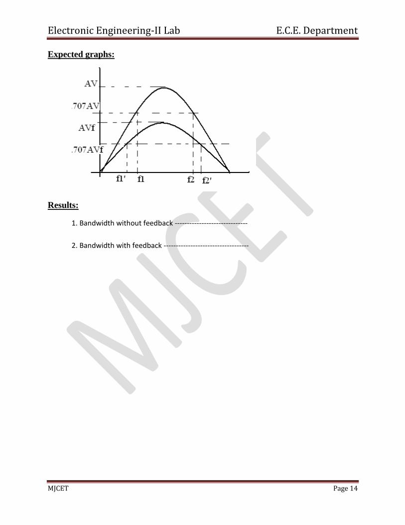
Expected graphs:
Results:
1. Bandwidth without feedback ------------------------------
2. Bandwidth with feedback -----------------------------------
Electronic Engineering-II Lab E.C.E. Department
MJCET Page 15
EXPERIMENT NO: 3
VOLTAGE SERIES FEEDBACK AMPLIFIER
Aim:
1. To plot the frequency response of a voltage series feedback amplifier
2. To see the effect of feed back upon gain and bandwidth,
Components:
Name Quantity
Transistor BC547 2
Resistor 100K , 8.2K , 820 , 680 , 120 , 4.7K , 2.2K , 2,4,1,1,1,1,1
Capacitor 10µF,100µF, 1 KPF 3, 2,1
Equipment:
Name Range Quantity
Bread Board 1
Dual DC power supply 0-30V 1
Function Generator (0-1)MHz 1
Digital Ammeter, Voltmeter [0-200µA/200mA], [0-20V] 1
CRO (0-20)MHz 1
CRO probes, Connecting Wires
Specifications:
For Transistor BC 547:
Max Collector Current= 0.1A
Vceo max= 50V
VEB0 = 6V
VCB0 = 50V
Collector power dissipation = 500mW
Temperature Range = -65 to +150 0C
hfe = 110 - 220
Theory:
Negative feedback is defined as a process of returning a part of the output signal to the input out
of phase with the input signal. It reduces gain and increases bandwidth. Negative feedback is
employed in amplifier circuits to improve the stability of the gain, reduce distortion and the
effect of noise. It also helps in obtaining desired values of input and output resistances.
A voltage series feedback amplifier samples output voltage and returns the feedback signal to the
input in series opposing. Feedback signal is a voltage signal.
Electronic Engineering-II Lab E.C.E. Department
MJCET Page 16
Of VV
Voltage series feedback increases input resistance and decreases output resistance.
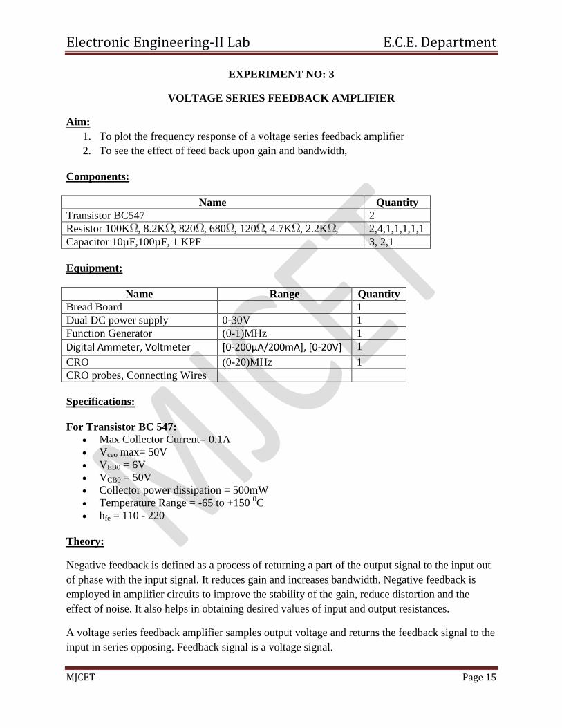
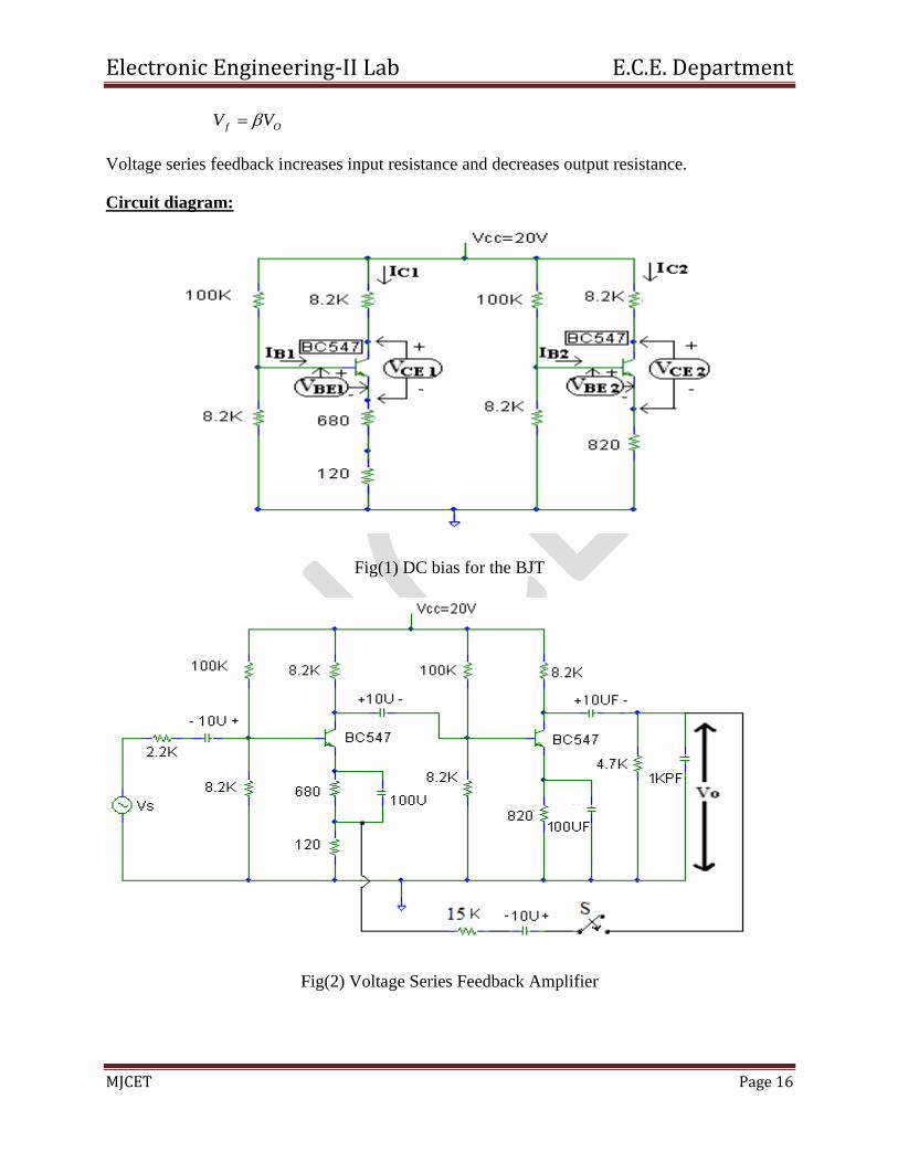
Circuit diagram:
Fig(1) DC bias for the BJT
Fig(2) Voltage Series Feedback Amplifier
Electronic Engineering-II Lab E.C.E. Department
MJCET Page 17
Procedure:
1. Connect the circuit as shown in figure 1. Note the DC conditions.
2. Connect the circuit as shown in figure 2. The switch must be open circuit, Then the
circuit does not has feedback.
3. Adjust the input signal frequency to 1 KHz and the peak to peak amplitude to 3mV. Note
the output voltage and calculate the gain.
4. Vary the frequency from 30 Hz to 500 KHz in appropriate steps and note VS and VO in
each case. Calculate the gain without feedback as S
O
vV
VA
.
5. Plot a graph between gain and frequency. Calculate bandwidth from the graph.
6. Now connect the switch as short circuit. This will introduce voltage series feedback in the
circuit. Repeat steps 3 to 5. in this case vary the frequency from 30 Hz to 2 MHz.
7. Compare the gain and bandwidth with and without feedback
Observations:
DC conditions:-
For stage-1, VBE1 = ……………. VCE1 = ………………
IB1 = ……………… IC1 = ………………..
For stage-2, VBE2 = ……………. VCE2 = ………………
IB2 = ……………… IC2 = ………………..
Frequency Response:-
Frequency Response:
Sl.No. Frequency Vi
(mV)
VO
(V)
VO f
(V) i
O
VV
VA
i
fO
fVV
VA

Electronic Engineering-II Lab E.C.E. Department
MJCET Page 18
Expected graph:
Fig(3) Frequency response of Voltage Series Feedback Amplifier
Result:
Gain without feedback = -----------
Bandwidth without feedback = ----------
Gain with feedback = -----------
Bandwidth with feedback = ----------

Electronic Engineering-II Lab E.C.E. Department
MJCET Page 19
EXPERIMENT NO: 4
CURRENT SHUNT FEEDBACK AMPLIFIER
Aim:
1. To plot the frequency response of a current shunt feedback amplifier
2. To see the effect of feed back upon gain and bandwidth,
Components:
Name Quantity
Transistor BC547 2
Resistor 100K , 8.2K , 820 , 680 , 120 , 4.7K , 2.2K , 2,4,1,1,1,1,1
Capacitor 10µF,100µF, 1 KPF 3, 2,1
Equipment:
Name Range Quantity
Bread Board 1
Dual DC power supply 0-30V 1
Function Generator (0-1)MHz 1
Digital Ammeter, Voltmeter [0-200µA/200mA], [0-20V] 1
CRO (0-20)MHz 1
CRO probes, Connecting Wires
Specifications:
For Transistor BC 547:
Max Collector Current= 0.1A
Vceo max= 50V
VEB0 = 6V
VCB0 = 50V
Collector power dissipation = 500mW
Temperature Range = -65 to +150 0C
hfe = 110 - 220
Theory:
Negative feedback is defined as a process of returning a part of the output signal to the input out
of phase with the input signal. It reduces gain and increases bandwidth. Negative feedback is
employed in amplifier circuits to improve the stability of the gain, reduce distortion and the
effect of noise. It also helps in obtaining desired values of input and output resistances.
A current shunt feedback amplifier samples output current and returns the feedback signal to the
input in shunt. Feedback signal is a voltage signal.
Electronic Engineering-II Lab E.C.E. Department
MJCET Page 20
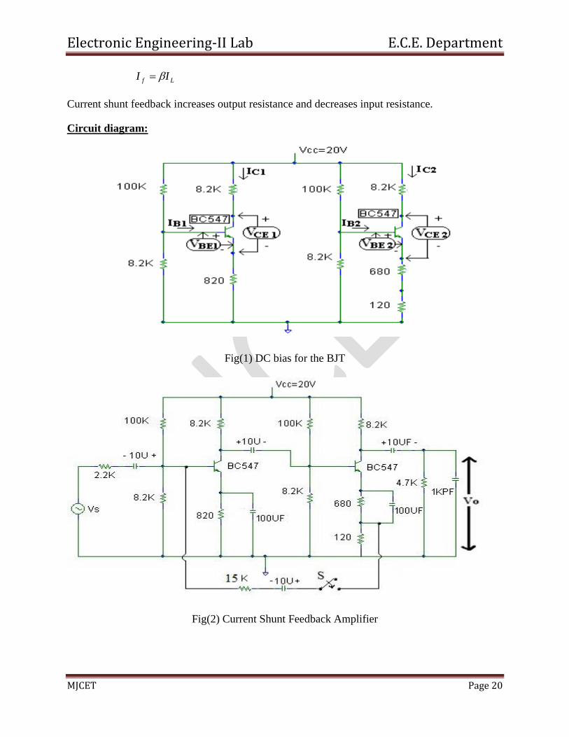
Lf II
Current shunt feedback increases output resistance and decreases input resistance.
Circuit diagram:
Fig(1) DC bias for the BJT
Fig(2) Current Shunt Feedback Amplifier
Electronic Engineering-II Lab E.C.E. Department
MJCET Page 21
Procedure:
1. Connect the circuit as shown in figure 1. Note the DC conditions.
2. Connect the circuit as shown in figure 2. The switch must be open circuit, Then the
circuit does not has feedback.
3. Adjust the input signal frequency to 1 KHz and the peak to peak amplitude to 3mV. Note
the output voltage and calculate the gain.
4. Vary the frequency from 30 Hz to 500 KHz in appropriate steps and note VS and VO in
each case. Calculate the gain without feedback as S
O
vV
VA
.
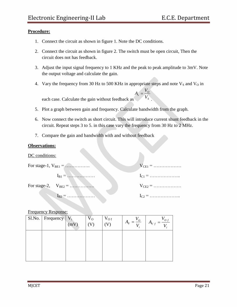
5. Plot a graph between gain and frequency. Calculate bandwidth from the graph.
6. Now connect the switch as short circuit. This will introduce current shunt feedback in the
circuit. Repeat steps 3 to 5. in this case vary the frequency from 30 Hz to 2 MHz.
7. Compare the gain and bandwidth with and without feedback
Observations:
DC conditions:
For stage-1, VBE1 = ……………. VCE1 = ………………
IB1 = ……………… IC1 = ………………..
For stage-2, VBE2 = ……………. VCE2 = ………………
IB2 = ……………… IC2 = ………………..
Frequency Response:
Sl.No. Frequency Vi
(mV)
VO
(V)
VO f
(V) i
O
VV
VA
i
fO
fVV
VA
Electronic Engineering-II Lab E.C.E. Department
MJCET Page 22
Expected graph:
Fig(3) frequency response of Current Shunt Feedback Amplifier
Result:
Gain without feedback = -----------
Bandwidth without feedback = ----------
Gain with feedback = -----------
Bandwidth with feedback = ----------
Electronic Engineering-II Lab E.C.E. Department
MJCET Page 23
Experiment No: 5
Voltage Shunt Feedback Amplifier
Aim: To plot the frequency response of a voltage shunt feedback amplifier and study the effect of
feedback on gain and bandwidth.
Circuit diagram:
Theory:
Negative feedback is defined as a process of returning a part of the output signal to the input out
of phase with the input signal. It reduces gain and increases bandwidth. Negative feedback is
employed in amplifier circuits to improve the stability of the gain, reduce distortion and the
effect of noise. It also helps in obtaining desired values of input and output resistances.
A current series feedback amplifier samples output current and returns the feedback signal to the
input in series opposing. Feedback signal is a voltage signal.
Lf IV
Current series feedback increases both input and output impedances.
Procedure:
1.Connect the circuit as shown in figure but with switch open. This circuit does not have
feedback.
2.Note the DC conditions.
Electronic Engineering-II Lab E.C.E. Department
MJCET Page 24
3.Adjust the input signal frequency to 1 KHz and the peak to peak amplitude to 30mV. Note the
output voltage and calculate the gain.
4.Vary the frequency from 30 Hz to 500 KHz in appropriate steps and note VS and VO in each
case. Calculate the gain without feedback asS
O
vV
VA .
5.Plot a graph between gain and frequency. Calculate bandwidth from the graph.
6.Close the switch now this will introduce the voltage shunt feedback
7. Repeat the above steps 1 to 5 again
8.Compare the gain and bandwidth with and without feedback.
Expected graph:
Observations:
Tabular Column: Vs=40 mV constant.
S# Frequency(Hz) V0 Vof AV=V0/VS AVF=VOf/VS
1
2
3
4
5
6
7
8
9
10
11
30
50
70
100
300
500
700
1K
3K
5K
7K

Electronic Engineering-II Lab E.C.E. Department
MJCET Page 25
12
13
14
15
16
17
18
19
20
10K
30K
50K
70K
100K
300K
500K
700K
1M
Calculations:
Theoretical Calculations:
Voltage gain without feedback is given by
Si
i
ie
Lfe
VRR
R
h
RhA
'
''
Voltage gain with feedback is given by
Si
i
i
Lfe
VfRR
R
R
RhA
'
''
where, efeiei RhhR )1(
Result:
Gain without feedback = -----------
Bandwidth without feedback = ----------
Gain with feedback = -----------
Bandwidth with feedback = ----------
Electronic Engineering-II Lab E.C.E. Department
MJCET Page 26
EXPERIMENT NO : 6
RC PHASE-SHIFT OSCILLATOR
Aim:
To design and study the operation of RC Phase-shift Oscillator using BJT and verify
Barkhausen‟s criterion.
Components:
Name Quantity
Transistor BC547 1
Resistor 74K , 15K , 4.7K , 1K , 6.8K,2.2K 1,1,2,1,2,1
Capacitor 10µF,100µF, 1 KPF 2, 1,3
Equipment:
Name Range Quantity
Bread Board 1
Dual DC power supply 0-30V 1
Function Generator (0-1)MHz 1
Digital Ammeter, Voltmeter [0-200µA/200mA], [0-20V] 1
CRO (0-20)MHz 1
CRO probes, Connecting Wires
Specifications:
For Transistor BC 547:
Max Collector Current= 0.1A
Vceo max= 50V
VEB0 = 6V
VCB0 = 50V
Collector power dissipation = 500mW
Temperature Range = -65 to +150 0C
hfe = 110 - 220
Theory:-
An oscillator is an electronic circuit that provides an AC output without using any AC input. All
Sinusoidal oscillator circuits use the concept of positive feedback to produce oscillations. An
oscillator circuit must satisfy the Barkhausen‟s criterion of unity loop gain to produce
oscillations.
Electronic Engineering-II Lab E.C.E. Department
MJCET Page 27
The Common Emitter amplifier provides a phase shift of 180˚. Additional 180˚ of phase shift
required to satisfy the Barkhausen‟s criterion of phase shift is provided by the RC phase-shifting
network. RC Phase-shift oscillator is used at Audio Frequencies.
Design:
Q: Design RC Phase-shift oscillator circuit to provide oscillations at a frequency of 8 KHz. Use
BJT BC547 for which β = 200, hfe = 50, hie = 1.5 KΩ and VBE(active) = 0.65V. The biasing
conditions are as follows.VCC = 12V, IC = 1mA, VCE = 6V and Stability factor is S = 10.
Use RC = 4.7KΩ.
Solution:
Use, BC II
AI B 5
Apply KVL to the output loop:
0 ECCECCCC RIVRIV
KRE 3.1
Apply Thevenin‟s theorem to the base
circuit, then
21
2
RR
RVV CC
B
And
21
21
RR
RRRB
We know that the stability factor for a self
bias circuit is given by,
EB
E
RR
RS
1
1
KRB 31.12
Apply KVL to the input loop, then
0 EEBEBBB RIVRIV
01.2 BV V
Divide RB with VB:
KV
RVR
B
BCC 5.731
Also, 21
21
RR
RRRB
KR 8.142
We know that KRCfo
462
1
where R
RK C
Assume that KR 8.6 . Then KPFC 1 .
Also RhR ie 3
KR 7.43
Circuit diagram:-
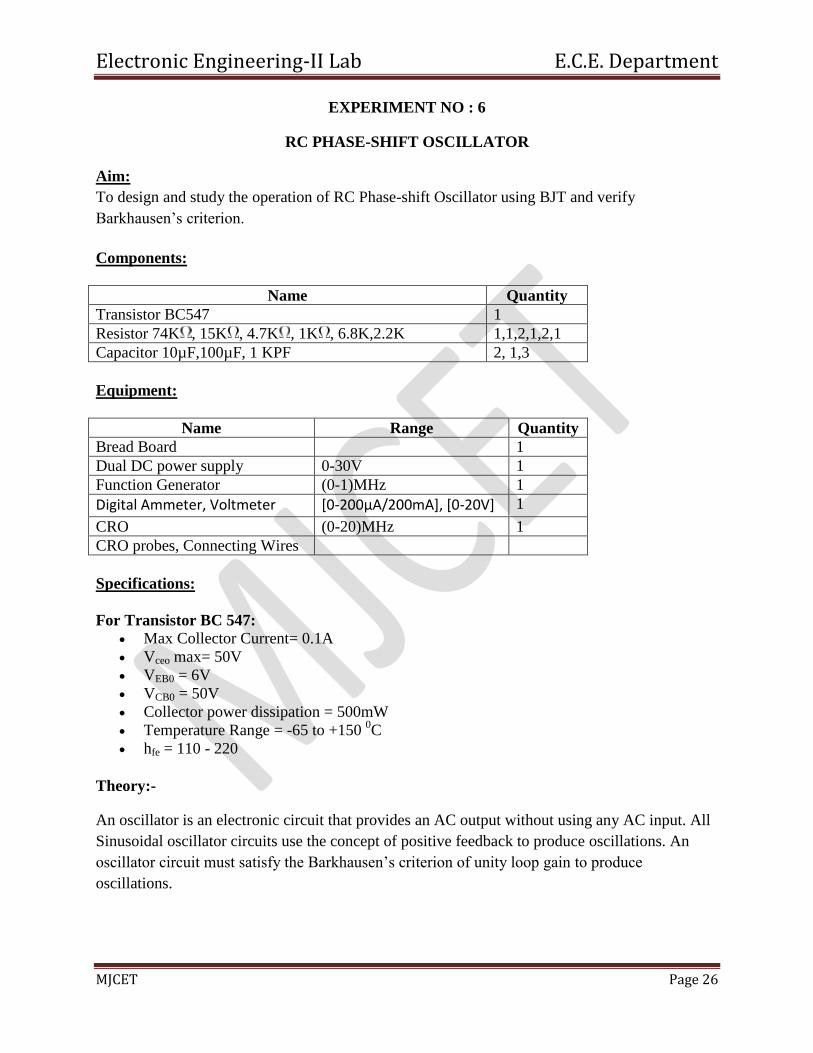
For Part-I:
Fig (1) : RC Phase shift oscillator
For Part-II:
Fig (2): Amplifier Circuit diagram
Fig (3): Feedback network

Electronic Engineering-II Lab E.C.E. Department
MJCET Page 29
Procedure:-
Part-I: Study of operation
1) Connect the self bias circuit and check the DC conditions.
2) Connect other components of the oscillator circuit as shown in figure. Observe the output
voltage waveform on CRO screen. Note down its peak to peak amplitude and frequency.
Part-II: Verification of Barkhausen’s criterion
1) Connect only the amplifier circuit and find its gain at the frequency of oscillations. Apply
an input of 30mV. Also observe the phase shift between input and output voltages.
2) Connect only the feedback network as shown and compute the feedback factor β as
S
f
V
V
.
3) Compute the loop gain as A . This product should be greater than or equal to unity.
4) Observe the phase shift between Vf and VS.
5) Add the phase shift provided by the amplifier and feedback network. The sum should be
equal to 360˚.
Observations: -
Draw the output waveform; mark its peak-to-peak amplitude and time period.
Result:-
Frequency of oscillations, fo = ------------
Peak to peak amplitude of output = -------------------
Loop gain = --------------------
Phase shift = ---------------------------
Hence Barkhausen‟s criterion is satisfied.
Electronic Engineering-II Lab E.C.E. Department
MJCET Page 30
EXPERIMENT NO: 7
COLPITTS OSCILLATOR
Aim:
To design and study the operation of colpitts Oscillator using BJT and determine the frequency
of oscillation.
Components:
Name Quantity
Transistor BC547 1
Resistor 74K , 15 K , 4.7K , 1K , 1,1,1,1
Capacitor 4.7µF, 1 KPF 2, 1
Inductor 70 μH 1
Equipment:
Name Range Quantity
Bread Board 1
Dual DC power supply 0-30V 1
Digital Ammeter, Voltmeter [0-200µA/200mA], [0-20V] 1
CRO (0-20)MHz 1
CRO probes, Connecting Wires
Specifications:
For Transistor BC 547:
Max Collector Current= 0.1A
Vceo max= 50V
VEB0 = 6V
VCB0 = 50V
Collector power dissipation = 500mW
Temperature Range = -65 to +150 0C
hfe = 110 - 220
Theory:-
An oscillator is an electronic circuit that provides an AC output without using any AC input. All
Sinusoidal oscillator circuits use the concept of positive feedback to produce oscillations. An
oscillator circuit must satisfy the Barkhausen‟s criterion of unity loop gain to produce
oscillations.
Colpitt‟s oscillator is a popular LC Oscillator circuit used at Radio Frequencies.
Electronic Engineering-II Lab E.C.E. Department
MJCET Page 31
Design:
Q: Design Colpitt‟s oscillator circuit to provide oscillations at a frequency of 850 KHz. Use BJT
BC547 for which β = 200, hfe = 50, hie = 1.5 KΩ and VBE(active) = 0.65V. The biasing conditions
are as follows.VCC = 12V, IC = 1mA, VCE = 6V and Stability factor is S = 10. Use RC = 4.7KΩ.
Solution:
Use, BC II
AI B 5
Apply KVL to the output loop:
0 ECCECCCC RIVRIV
KRE 3.1
Apply Thevenin‟s theorem to the base
circuit, then
21
2
RR
RVV CC
B
And
21
21
RR
RRRB
We know that the stability factor for a self
bias circuit is given by,
EB
E
RR
RS
1
1
KRB 31.12
Apply KVL to the input loop, then
0 EEBEBBB RIVRIV
01.2 BV V
Divide RB with VB:
KV
RVR
B
BCC 5.731
Also, 21
21
RR
RRRB
KR 8.142
We know that
)11
(1
2
1
21 CCLfo
Assume that KPFCC 121 . Then
HL 70
Circuit diagram:-
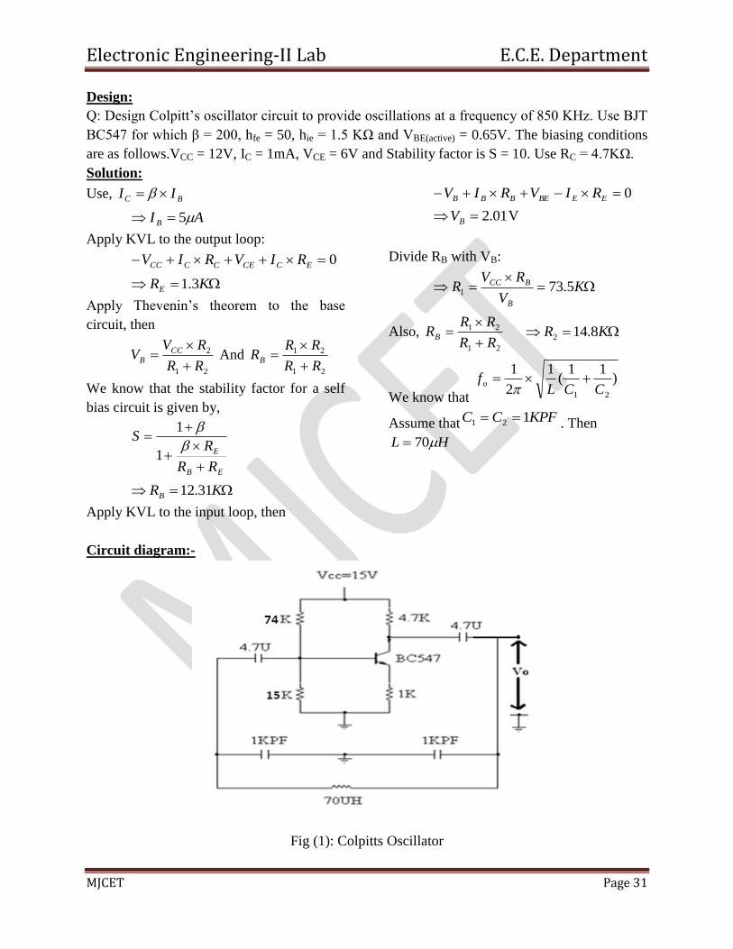
Fig (1): Colpitts Oscillator
MJCET Page 32
Procedure:-
1) Connect the self bias circuit and check the DC conditions.
2) Connect other components of the oscillator circuit as shown in figure 1. Adjust the
capacitance to 800 PF.
3) Observe the output voltage waveform on CRO screen. Note down its peak to peak
amplitude and frequency.
4) Vary the inductance in appropriate steps and record the frequency in each case.
5) Calculate the frequency theoretically and record it in the table. Compare the theoretical
and practical values.
Observations:-
DC conditions:-
VBE = ……………. VCE = ………………
IB = ……………… IC = ………………..
Sl. No.
Inductance
(μH)
Frequency
(Practically)
(KHz)
Frequency
)11
(1
2
1
21 CCLfo
Result:-
Colpitts oscillator circuit is designed for the given specifications and its operation is studied.
MJCET Page 33
EXPERIMENT NO: 8
HARTLEY OSCILLATOR
Aim:
To design and study the operation of Hartley Oscillator using BJT and determine the frequency
of oscillation.
Components:
Name Quantity
Transistor BC547 1
Resistor 74K , 15 K , 4.7K , 1K , 1,1,1,1
Capacitor 4.7µF, 100 PF 2, 1
Inductor 70 μH 2
Equipment:
Name Range Quantity
Bread Board 1
Dual DC power supply 0-30V 1
Digital Ammeter, Voltmeter [0-200µA/200mA], [0-20V] 1
CRO (0-20)MHz 1
CRO probes, Connecting Wires
Specifications:
For Transistor BC 547:
Max Collector Current= 0.1A
Vceo max= 50V
VEB0 = 6V
VCB0 = 50V
Collector power dissipation = 500mW
Temperature Range = -65 to +150 0C
hfe = 110 - 220
Theory:-
An oscillator is an electronic circuit that provides an AC output without using any AC input. All
Sinusoidal oscillator circuits use the concept of positive feedback to produce oscillations. An
oscillator circuit must satisfy the Barkhausen‟s criterion of unity loop gain to produce
oscillations.
Hartley‟s oscillator is a popular LC Oscillator circuit used at Radio Frequencies.
MJCET Page 34
Design:
Q: Design Hartley‟s oscillator circuit to provide oscillations at a frequency of 850 KHz. Use BJT
BC547 for which β = 200, hfe = 50, hie = 1.5 KΩ and VBE(active) = 0.65V. The biasing conditions
are as follows.VCC = 12V, IC = 1mA, VCE = 6V and Stability factor is S = 10. Use RC = 4.7KΩ.
Solution:
Use, BC II
AI B 5
Apply KVL to the output loop:
0 ECCECCCC RIVRIV
KRE 3.1
Apply Thevenin‟s theorem to the base
circuit, then
21
2
RR
RVV CC
B
And
21
21
RR
RRRB
We know that the stability factor for a self
bias circuit is given by,
EB
E
RR
RS
1
1
KRB 31.12
Apply KVL to the input loop, then
0 EEBEBBB RIVRIV
01.2 BV V
Divide RB with VB:
KV
RVR
B
BCC 5.731
Also, 21
21
RR
RRRB
KR 8.142
We know that CMLL
fo)2(2
1
21
Assume that HLL 7021 and
HM 45 . Then 100C PF.

Department of ECE Page 35
Circuit diagram:-
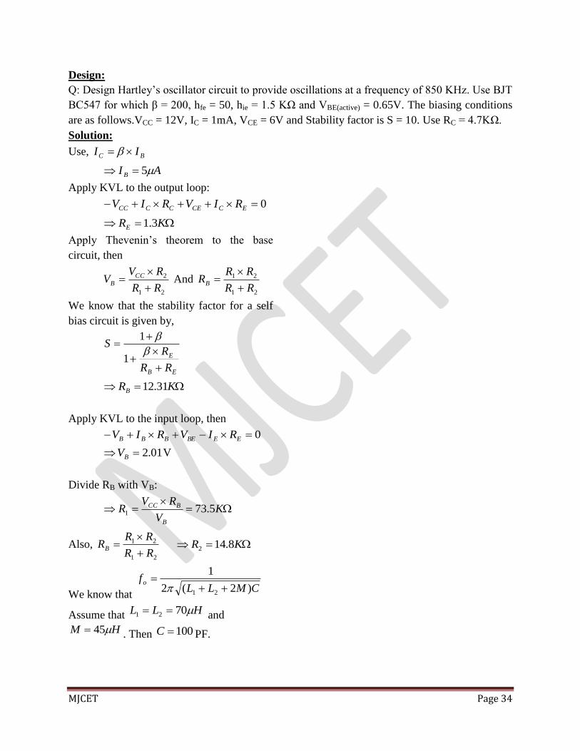
Fig (1): Hartley‟s Oscillator
Procedure:-
1) Connect the self bias circuit and check the DC conditions.
2) Connect other components of the oscillator circuit as shown in figure. Adjust the
capacitance to 800 PF.
3) Observe the output voltage waveform on CRO screen. Note down its peak to peak
amplitude and frequency.
4) Vary the capacitance in appropriate steps and record the frequency in each case.
5) Calculate the frequency theoretically also and record it in the table. Compare the
theoretical and practical values.
Observations:-
DC conditions:-
VBE = ……………. VCE = ………………
IB = ……………… IC = ………………..

Department of ECE Page 36
Sl. No.
Capacitance
(PF)
Frequency
(Practically)
(MHz)
Frequency
CMLLfo
)2(2
1
21
Result:-
Hartley oscillator circuit is designed for the given specifications and its operation is studied.

Department of ECE Page 37
Experiment No. 9
Clippers
AIM:-TO Study the positive Peak, Positive Base , Negative peak , Negative Base & Double
ended Clipper Circuits for Different reference Voltages (0,1v,2v)& Observe the output.
APPARATUS REQUIRED:-
1. Diode -1N4148
2. Resistor -56K
3. DC Regulated Power Supply
4. Signal Generator & CRO
CIRCIUT DIGARAMS:-

Department of ECE Page 38
Expected Graphs:-
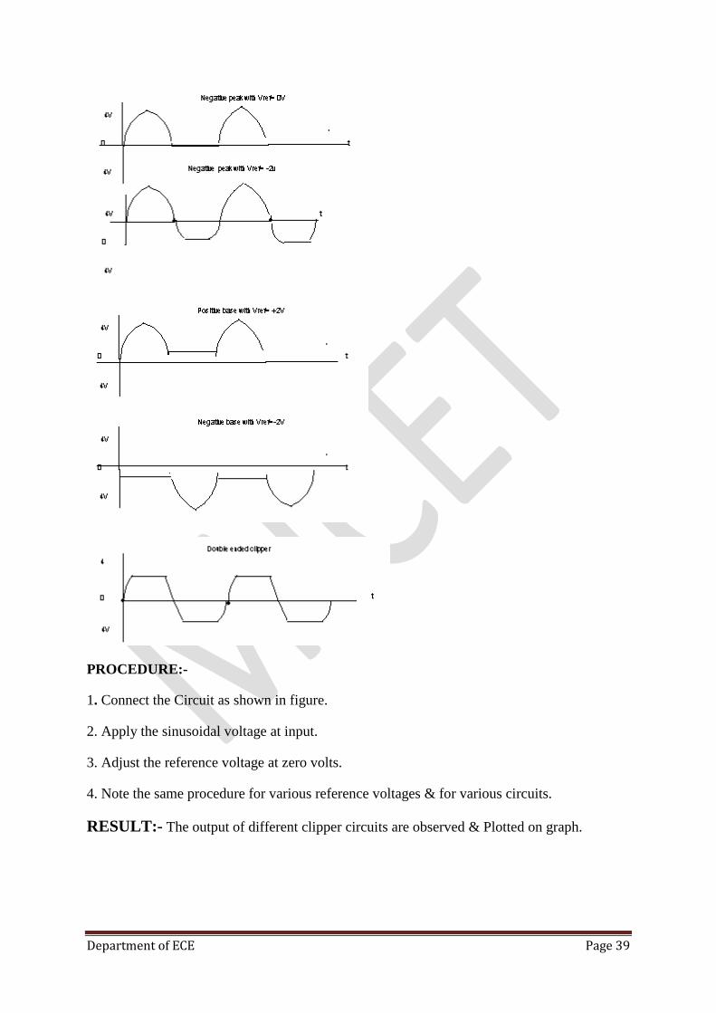
Department of ECE Page 39
PROCEDURE:-
1. Connect the Circuit as shown in figure.
2. Apply the sinusoidal voltage at input.
3. Adjust the reference voltage at zero volts.
4. Note the same procedure for various reference voltages & for various circuits.
RESULT:- The output of different clipper circuits are observed & Plotted on graph.
Department of ECE Page 40
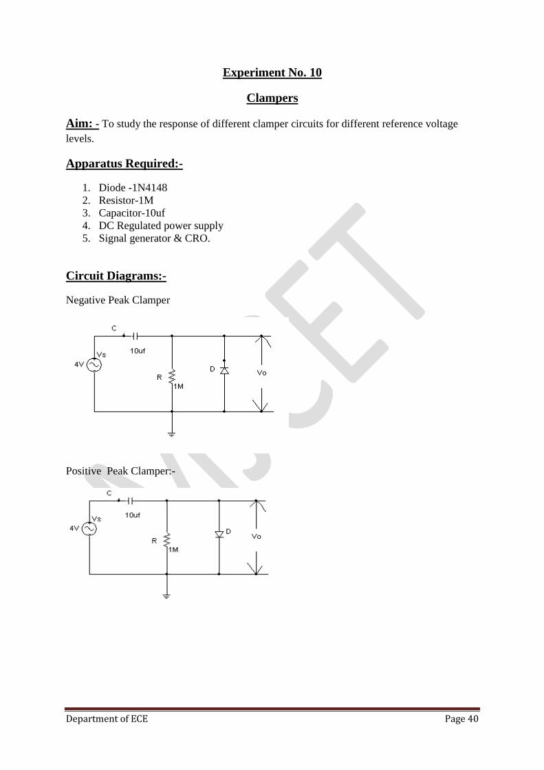
Experiment No. 10
Clampers
Aim: - To study the response of different clamper circuits for different reference voltage
levels.
Apparatus Required:-
1. Diode -1N4148
2. Resistor-1M
3. Capacitor-10uf
4. DC Regulated power supply
5. Signal generator & CRO.
Circuit Diagrams:-
Negative Peak Clamper
Positive Peak Clamper:-
Department of ECE Page 41
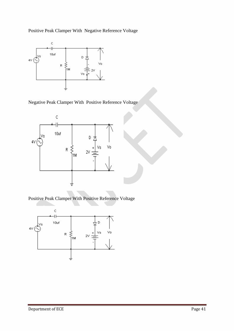
Positive Peak Clamper With Negative Reference Voltage
Negative Peak Clamper With Positive Reference Voltage
Positive Peak Clamper With Positive Reference Voltage
Department of ECE Page 42
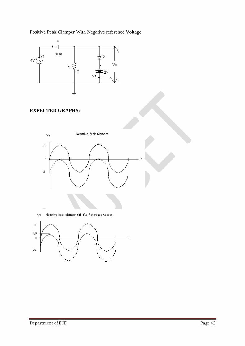
Positive Peak Clamper With Negative reference Voltage
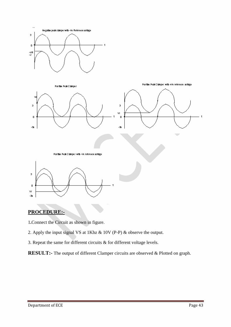
EXPECTED GRAPHS:-
Department of ECE Page 43
PROCEDURE:-
1.Connect the Circuit as shown in figure.
2. Apply the input signal VS at 1Khz & 10V (P-P) & observe the output.
3. Repeat the same for different circuits & for different voltage levels.
RESULT:- The output of different Clamper circuits are observed & Plotted on graph.

Department of ECE Page 44
APPENDIX
LABORATORY COURSE ASSESSMENT GUIDELINES
i. The number of experiments in each laboratory course shall be as per the curriculum in
the scheme of instructions provided by OU. Mostly the number of experiments is 10
in each laboratory course under semester scheme and 18 under year wise scheme.
ii. The students will maintain a separate note book for observations in each laboratory
course.
iii. In each session the students will conduct the allotted experiment and enter the data in
the observation table.
iv. The students will then complete the calculations and obtain the results. The course
coordinator will certify the result in the same session.
v. The students will submit the record in the next class. The evaluation will be
continuous and not cycle-wise or at semester end.
vi. The internal marks of 25 are awarded in the following manner:
a. Laboratory record - Maximum Marks 15
b. Test and Viva Voce - Maximum Marks 10
vii. Laboratory Record: Each experimental record is evaluated for a score of 50. The
rubric parameters are as follows: a. Write up format - Maximum Score 15
b. Experimentation Observations & Calculations - Maximum Score 20
c. Results and Graphs - Maximum Score 10
d. Discussion of results - Maximum Score 5
While (a), (c) and (d) are assessed at the time of record submission, (b) is assessed during the
session based on the observations and calculations. Hence if a student is absent for an
experiment but completes it in another session and subsequently submits the record, it shall
be evaluated for a score of 30 and not 50.
viii. The experiment evaluation rubric is therefore as follows:
Parameter Max Score Outstanding Accomplished Developing Beginner Points
Observations
and
Calculations
20
Write up
format 15
Results and
graphs 10
Discussion of
Results 5
Department of ECE Page 45
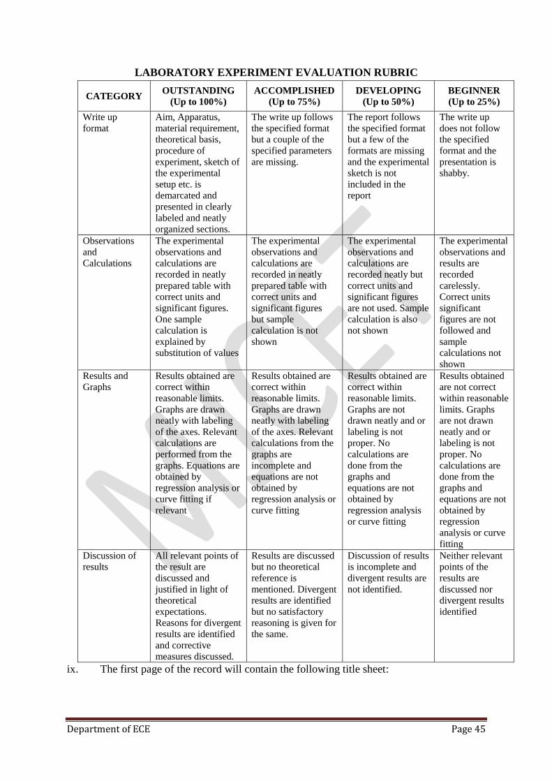
LABORATORY EXPERIMENT EVALUATION RUBRIC
CATEGORY OUTSTANDING
(Up to 100%)
ACCOMPLISHED
(Up to 75%)
DEVELOPING
(Up to 50%)
BEGINNER
(Up to 25%)
Write up
format
Aim, Apparatus,
material requirement,
theoretical basis,
procedure of
experiment, sketch of
the experimental
setup etc. is
demarcated and
presented in clearly
labeled and neatly
organized sections.
The write up follows
the specified format
but a couple of the
specified parameters
are missing.
The report follows
the specified format
but a few of the
formats are missing
and the experimental
sketch is not
included in the
report
The write up
does not follow
the specified
format and the
presentation is
shabby.
Observations
and
Calculations
The experimental
observations and
calculations are
recorded in neatly
prepared table with
correct units and
significant figures.
One sample
calculation is
explained by
substitution of values
The experimental
observations and
calculations are
recorded in neatly
prepared table with
correct units and
significant figures
but sample
calculation is not
shown
The experimental
observations and
calculations are
recorded neatly but
correct units and
significant figures
are not used. Sample
calculation is also
not shown
The experimental
observations and
results are
recorded
carelessly.
Correct units
significant
figures are not
followed and
sample
calculations not
shown
Results and
Graphs
Results obtained are
correct within
reasonable limits.
Graphs are drawn
neatly with labeling
of the axes. Relevant
calculations are
performed from the
graphs. Equations are
obtained by
regression analysis or
curve fitting if
relevant
Results obtained are
correct within
reasonable limits.
Graphs are drawn
neatly with labeling
of the axes. Relevant
calculations from the
graphs are
incomplete and
equations are not
obtained by
regression analysis or
curve fitting
Results obtained are
correct within
reasonable limits.
Graphs are not
drawn neatly and or
labeling is not
proper. No
calculations are
done from the
graphs and
equations are not
obtained by
regression analysis
or curve fitting
Results obtained
are not correct
within reasonable
limits. Graphs
are not drawn
neatly and or
labeling is not
proper. No
calculations are
done from the
graphs and
equations are not
obtained by
regression
analysis or curve
fitting
Discussion of
results
All relevant points of
the result are
discussed and
justified in light of
theoretical
expectations.
Reasons for divergent
results are identified
and corrective
measures discussed.
Results are discussed
but no theoretical
reference is
mentioned. Divergent
results are identified
but no satisfactory
reasoning is given for
the same.
Discussion of results
is incomplete and
divergent results are
not identified.
Neither relevant
points of the
results are
discussed nor
divergent results
identified
ix. The first page of the record will contain the following title sheet:

Department of ECE Page 46
SAMPLE ASSESSMENT SHEET
NAME: ROLL NO.
Exp.
No.
Date
conducted
Date
Submitted
Observations
&Calculations
(Max 20)
Write up
(Max 15)
Results and
Graphs
(Max 10)
Discussion
of Results
(Max 5)
Total Score
(Max 50)
1
2
3
4
5
6
7
8
9
10
11
12
x. The 15 marks of laboratory record will be scaled down from the TOTAL of the
assessment sheet.
xi. The test and viva voce will be scored for 10 marks as follows:
Internal Test - 6 marks
Viva Voce / Quiz - 4 marks
xii. Each laboratory course shall have 5 course outcomes.

Department of ECE Page 47
The proposed course outcomes are as follows:
On successful completion of the course, the student will acquire the ability to:
1. Conduct experiments, take measurements and analyze the data through hands-on
experience in order to demonstrate understanding of the theoretical concepts of
_______________________, while working in small groups.
2. Demonstrate writing skills through clear laboratory reports.
3. Employ graphics packages for drawing of graphs and use computational software for
statistical analysis of data.
4. Compare the experimental results with those introduced in lecture, draw relevant
conclusions and substantiate them satisfactorily.
5. Transfer group experience to individual performance of experiments and demonstrate
effective oral communication skills.
xiii. The Course coordinators would prepare the assessment matrix in accordance with the
guidelines provided above for the five course outcomes. The scores to be entered
against each of the course outcome would be the sum of the following as obtained
from the assessment sheet in the record:
a. Course Outcome 1: Sum of the scores under „Observations and Calculations‟.
b. Course Outcome 2: Sum of the scores under „Write up‟.
c. Course Outcome 3: Sum of the scores under „Results and Graphs‟.
d. Course Outcome 4: Sum of the scores under „Discussion of Results‟.
e. Course Outcome 5: Marks for „Internal Test and Viva voce‟.
xiv. Soft copy of the assessment matrix would be provided to the course coordinators.

Department of ECE Page 48
MUFFAKHAM JAH COLLEGE OF ENGINEERING AND TECHNOLOGY
Program Outcomes of B.E (ECE) Program:
PO1: Engineering knowledge: Apply the knowledge of mathematics, science, engineering fundamentals, and an
engineering specialization to the solution of complex engineering problems.
PO2: Problem analysis: Identify, formulate, research literature, and analyse complex engineering problems
reaching substantiated conclusions using first principles of mathematics, natural sciences, and engineering
sciences
PO3: Design/development of solutions: Design solutions for complex engineering problems and design system
components or processes that meet the specified needs with appropriate consideration for the public health and
safety, and the cultural, societal, and environmental considerations.
PO4: Conduct investigations of complex problems: Use research-based knowledge and research methods
including design of experiments, analysis and interpretation of data, and synthesis of the information to provide
valid conclusions.
PO5: Modern tool usage: Create, select, and apply appropriate techniques, resources, and modern engineering
and IT tools including prediction and modeling to complex engineering activities with an understanding of the
limitations.
PO6: The engineer and society: Apply reasoning informed by the contextual knowledge to assess societal,
health, safety, legal, and cultural issues and the consequent responsibilities relevant to the professional
engineering practice.
PO7: Environment and sustainability: Understand the impact of the professional engineering solutions in
societal and environmental contexts, and demonstrate the knowledge of, and need for sustainable development.
PO8: Ethics: Apply ethical principles and commit to professional ethics and responsibilities and norms of the
engineering practice.
PO9: Individual and team work: Function effectively as an individual, and as a member or leader in diverse
teams, and in multidisciplinary settings.
PO10: Communication: Communicate effectively on complex engineering activities with the engineering
community and with society at large, such as, being able to comprehend and write effective reports and design
documentation, make effective presentations, and give and receive clear instructions.
PO11: Project management and finance: Demonstrate knowledge and understanding of the engineering and
management principles and apply these to one‟s own work, as a member and leader in a team, to manage
projects and in multidisciplinary environments.
PO 12: Life-long learning: Recognise the need for, and have the preparation and ability to engage in
independent and life-long learning in the broadest context of technological change.
Program Specific Outcomes (PSOs) of ECE Department, MJCET
PSO1: The ECE Graduates will acquire state of art analysis and design skills in the areas of digital and analog
VLSI Design using modern CAD tools.
PSO2: The ECE Graduates will develop preliminary skills and capabilities necessary for embedded system
design and demonstrate understanding of its societal impact.
PSO3: The ECE Graduates will obtain the knowledge of the working principles of modern communication
systems and be able to develop simulation models of components of a communication system.
PSO4: The ECE Graduates will develop soft skills, aptitude and programming skills to be employable in IT
sector.
Related Documents