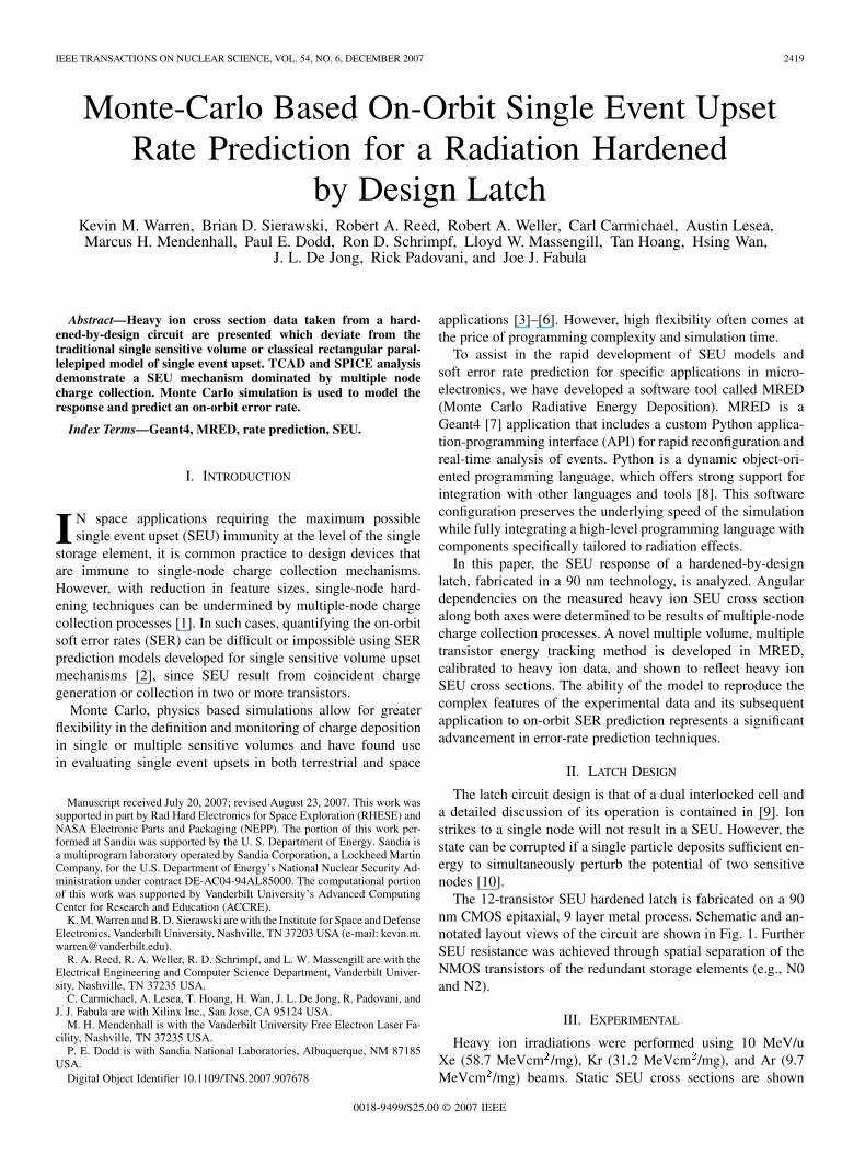
IEEE TRANSACTIONS ON NUCLEAR SCIENCE, VOL. 54, NO. 6, DECEMBER 2007 2419 Monte-Carlo Based On-Orbit Single Event Upset Rate Prediction for a Radiation Hardened by Design Latch Kevin M. Warren, Brian D. Sierawski, Robert A. Reed, Robert A. Weller, Carl Carmichael, Austin Lesea, Marcus H. Mendenhall, Paul E. Dodd, Ron D. Schrimpf, Lloyd W. Massengill, Tan Hoang, Hsing Wan, J. L. De Jong, Rick Padovani, and Joe J. Fabula Abstract—Heavy ion cross section data taken from a hard- ened-by-design circuit are presented which deviate from the traditional single sensitive volume or classical rectangular paral- lelepiped model of single event upset. TCAD and SPICE analysis demonstrate a SEU mechanism dominated by multiple node charge collection. Monte Carlo simulation is used to model the response and predict an on-orbit error rate. Index Terms—Geant4, MRED, rate prediction, SEU. I. INTRODUCTION I N space applications requiring the maximum possible single event upset (SEU) immunity at the level of the single storage element, it is common practice to design devices that are immune to single-node charge collection mechanisms. However, with reduction in feature sizes, single-node hard- ening techniques can be undermined by multiple-node charge collection processes [1]. In such cases, quantifying the on-orbit soft error rates (SER) can be difficult or impossible using SER prediction models developed for single sensitive volume upset mechanisms [2], since SEU result from coincident charge generation or collection in two or more transistors. Monte Carlo, physics based simulations allow for greater flexibility in the definition and monitoring of charge deposition in single or multiple sensitive volumes and have found use in evaluating single event upsets in both terrestrial and space Manuscript received July 20, 2007; revised August 23, 2007. This work was supported in part by Rad Hard Electronics for Space Exploration (RHESE) and NASA Electronic Parts and Packaging (NEPP). The portion of this work per- formed at Sandia was supported by the U. S. Department of Energy. Sandia is a multiprogram laboratory operated by Sandia Corporation, a Lockheed Martin Company, for the U.S. Department of Energy’s National Nuclear Security Ad- ministration under contract DE-AC04-94AL85000. The computational portion of this work was supported by Vanderbilt University’s Advanced Computing Center for Research and Education (ACCRE). K. M. Warren and B. D. Sierawski are with the Institute for Space and Defense Electronics, Vanderbilt University, Nashville, TN 37203 USA (e-mail: kevin.m. [email protected]). R. A. Reed, R. A. Weller, R. D. Schrimpf, and L. W. Massengill are with the Electrical Engineering and Computer Science Department, Vanderbilt Univer- sity, Nashville, TN 37235 USA. C. Carmichael, A. Lesea, T. Hoang, H. Wan, J. L. De Jong, R. Padovani, and J. J. Fabula are with Xilinx Inc., San Jose, CA 95124 USA. M. H. Mendenhall is with the Vanderbilt University Free Electron Laser Fa- cility, Nashville, TN 37235 USA. P. E. Dodd is with Sandia National Laboratories, Albuquerque, NM 87185 USA. Digital Object Identifier 10.1109/TNS.2007.907678 applications [3]–[6]. However, high flexibility often comes at the price of programming complexity and simulation time. To assist in the rapid development of SEU models and soft error rate prediction for specific applications in micro- electronics, we have developed a software tool called MRED (Monte Carlo Radiative Energy Deposition). MRED is a Geant4 [7] application that includes a custom Python applica- tion-programming interface (API) for rapid reconfiguration and real-time analysis of events. Python is a dynamic object-ori- ented programming language, which offers strong support for integration with other languages and tools [8]. This software configuration preserves the underlying speed of the simulation while fully integrating a high-level programming language with components specifically tailored to radiation effects. In this paper, the SEU response of a hardened-by-design latch, fabricated in a 90 nm technology, is analyzed. Angular dependencies on the measured heavy ion SEU cross section along both axes were determined to be results of multiple-node charge collection processes. A novel multiple volume, multiple transistor energy tracking method is developed in MRED, calibrated to heavy ion data, and shown to reflect heavy ion SEU cross sections. The ability of the model to reproduce the complex features of the experimental data and its subsequent application to on-orbit SER prediction represents a significant advancement in error-rate prediction techniques. II. LATCH DESIGN The latch circuit design is that of a dual interlocked cell and a detailed discussion of its operation is contained in [9]. Ion strikes to a single node will not result in a SEU. However, the state can be corrupted if a single particle deposits sufficient en- ergy to simultaneously perturb the potential of two sensitive nodes [10]. The 12-transistor SEU hardened latch is fabricated on a 90 nm CMOS epitaxial, 9 layer metal process. Schematic and an- notated layout views of the circuit are shown in Fig. 1. Further SEU resistance was achieved through spatial separation of the NMOS transistors of the redundant storage elements (e.g., N0 and N2). III. EXPERIMENTAL Heavy ion irradiations were performed using 10 MeV/u Xe (58.7 MeVcm /mg), Kr (31.2 MeVcm /mg), and Ar (9.7 MeVcm /mg) beams. Static SEU cross sections are shown 0018-9499/$25.00 © 2007 IEEE

Welcome message from author
This document is posted to help you gain knowledge. Please leave a comment to let me know what you think about it! Share it to your friends and learn new things together.
Transcript
IEEE TRANSACTIONS ON NUCLEAR SCIENCE, VOL. 54, NO. 6, DECEMBER 2007 2419
Monte-Carlo Based On-Orbit Single Event UpsetRate Prediction for a Radiation Hardened
by Design LatchKevin M. Warren, Brian D. Sierawski, Robert A. Reed, Robert A. Weller, Carl Carmichael, Austin Lesea,Marcus H. Mendenhall, Paul E. Dodd, Ron D. Schrimpf, Lloyd W. Massengill, Tan Hoang, Hsing Wan,
J. L. De Jong, Rick Padovani, and Joe J. Fabula
Abstract—Heavy ion cross section data taken from a hard-ened-by-design circuit are presented which deviate from thetraditional single sensitive volume or classical rectangular paral-lelepiped model of single event upset. TCAD and SPICE analysisdemonstrate a SEU mechanism dominated by multiple nodecharge collection. Monte Carlo simulation is used to model theresponse and predict an on-orbit error rate.
Index Terms—Geant4, MRED, rate prediction, SEU.
I. INTRODUCTION
I N space applications requiring the maximum possiblesingle event upset (SEU) immunity at the level of the single
storage element, it is common practice to design devices thatare immune to single-node charge collection mechanisms.However, with reduction in feature sizes, single-node hard-ening techniques can be undermined by multiple-node chargecollection processes [1]. In such cases, quantifying the on-orbitsoft error rates (SER) can be difficult or impossible using SERprediction models developed for single sensitive volume upsetmechanisms [2], since SEU result from coincident chargegeneration or collection in two or more transistors.
Monte Carlo, physics based simulations allow for greaterflexibility in the definition and monitoring of charge depositionin single or multiple sensitive volumes and have found usein evaluating single event upsets in both terrestrial and space
Manuscript received July 20, 2007; revised August 23, 2007. This work wassupported in part by Rad Hard Electronics for Space Exploration (RHESE) andNASA Electronic Parts and Packaging (NEPP). The portion of this work per-formed at Sandia was supported by the U. S. Department of Energy. Sandia isa multiprogram laboratory operated by Sandia Corporation, a Lockheed MartinCompany, for the U.S. Department of Energy’s National Nuclear Security Ad-ministration under contract DE-AC04-94AL85000. The computational portionof this work was supported by Vanderbilt University’s Advanced ComputingCenter for Research and Education (ACCRE).
K. M. Warren and B. D. Sierawski are with the Institute for Space and DefenseElectronics, Vanderbilt University, Nashville, TN 37203 USA (e-mail: [email protected]).
R. A. Reed, R. A. Weller, R. D. Schrimpf, and L. W. Massengill are with theElectrical Engineering and Computer Science Department, Vanderbilt Univer-sity, Nashville, TN 37235 USA.
C. Carmichael, A. Lesea, T. Hoang, H. Wan, J. L. De Jong, R. Padovani, andJ. J. Fabula are with Xilinx Inc., San Jose, CA 95124 USA.
M. H. Mendenhall is with the Vanderbilt University Free Electron Laser Fa-cility, Nashville, TN 37235 USA.
P. E. Dodd is with Sandia National Laboratories, Albuquerque, NM 87185USA.
Digital Object Identifier 10.1109/TNS.2007.907678
applications [3]–[6]. However, high flexibility often comes atthe price of programming complexity and simulation time.
To assist in the rapid development of SEU models andsoft error rate prediction for specific applications in micro-electronics, we have developed a software tool called MRED(Monte Carlo Radiative Energy Deposition). MRED is aGeant4 [7] application that includes a custom Python applica-tion-programming interface (API) for rapid reconfiguration andreal-time analysis of events. Python is a dynamic object-ori-ented programming language, which offers strong support forintegration with other languages and tools [8]. This softwareconfiguration preserves the underlying speed of the simulationwhile fully integrating a high-level programming language withcomponents specifically tailored to radiation effects.
In this paper, the SEU response of a hardened-by-designlatch, fabricated in a 90 nm technology, is analyzed. Angulardependencies on the measured heavy ion SEU cross sectionalong both axes were determined to be results of multiple-nodecharge collection processes. A novel multiple volume, multipletransistor energy tracking method is developed in MRED,calibrated to heavy ion data, and shown to reflect heavy ionSEU cross sections. The ability of the model to reproduce thecomplex features of the experimental data and its subsequentapplication to on-orbit SER prediction represents a significantadvancement in error-rate prediction techniques.
II. LATCH DESIGN
The latch circuit design is that of a dual interlocked cell anda detailed discussion of its operation is contained in [9]. Ionstrikes to a single node will not result in a SEU. However, thestate can be corrupted if a single particle deposits sufficient en-ergy to simultaneously perturb the potential of two sensitivenodes [10].
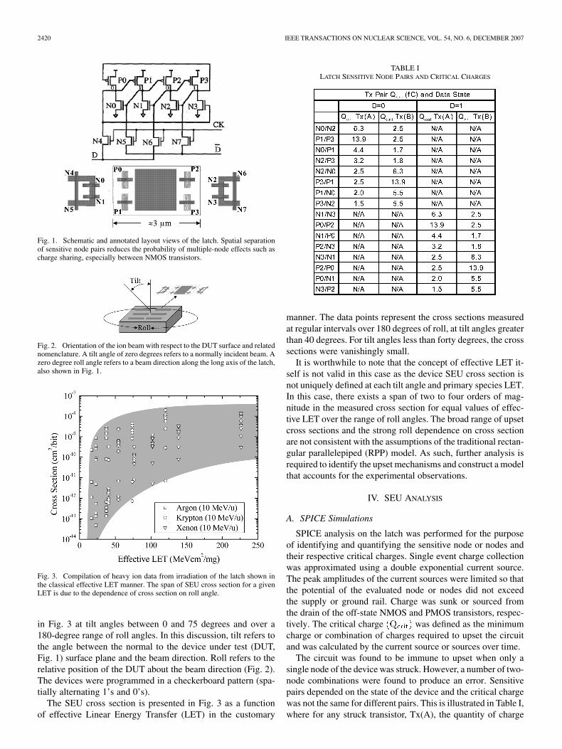
The 12-transistor SEU hardened latch is fabricated on a 90nm CMOS epitaxial, 9 layer metal process. Schematic and an-notated layout views of the circuit are shown in Fig. 1. FurtherSEU resistance was achieved through spatial separation of theNMOS transistors of the redundant storage elements (e.g., N0and N2).
III. EXPERIMENTAL
Heavy ion irradiations were performed using 10 MeV/uXe (58.7 MeVcm /mg), Kr (31.2 MeVcm /mg), and Ar (9.7MeVcm /mg) beams. Static SEU cross sections are shown
0018-9499/$25.00 © 2007 IEEE
2420 IEEE TRANSACTIONS ON NUCLEAR SCIENCE, VOL. 54, NO. 6, DECEMBER 2007
Fig. 1. Schematic and annotated layout views of the latch. Spatial separationof sensitive node pairs reduces the probability of multiple-node effects such ascharge sharing, especially between NMOS transistors.
Fig. 2. Orientation of the ion beam with respect to the DUT surface and relatednomenclature. A tilt angle of zero degrees refers to a normally incident beam. Azero degree roll angle refers to a beam direction along the long axis of the latch,also shown in Fig. 1.
Fig. 3. Compilation of heavy ion data from irradiation of the latch shown inthe classical effective LET manner. The span of SEU cross section for a givenLET is due to the dependence of cross section on roll angle.
in Fig. 3 at tilt angles between 0 and 75 degrees and over a180-degree range of roll angles. In this discussion, tilt refers tothe angle between the normal to the device under test (DUT,Fig. 1) surface plane and the beam direction. Roll refers to therelative position of the DUT about the beam direction (Fig. 2).The devices were programmed in a checkerboard pattern (spa-tially alternating 1’s and 0’s).
The SEU cross section is presented in Fig. 3 as a functionof effective Linear Energy Transfer (LET) in the customary
TABLE ILATCH SENSITIVE NODE PAIRS AND CRITICAL CHARGES
manner. The data points represent the cross sections measuredat regular intervals over 180 degrees of roll, at tilt angles greaterthan 40 degrees. For tilt angles less than forty degrees, the crosssections were vanishingly small.
It is worthwhile to note that the concept of effective LET it-self is not valid in this case as the device SEU cross section isnot uniquely defined at each tilt angle and primary species LET.In this case, there exists a span of two to four orders of mag-nitude in the measured cross section for equal values of effec-tive LET over the range of roll angles. The broad range of upsetcross sections and the strong roll dependence on cross sectionare not consistent with the assumptions of the traditional rectan-gular parallelepiped (RPP) model. As such, further analysis isrequired to identify the upset mechanisms and construct a modelthat accounts for the experimental observations.
IV. SEU ANALYSIS
A. SPICE Simulations
SPICE analysis on the latch was performed for the purposeof identifying and quantifying the sensitive node or nodes andtheir respective critical charges. Single event charge collectionwas approximated using a double exponential current source.The peak amplitudes of the current sources were limited so thatthe potential of the evaluated node or nodes did not exceedthe supply or ground rail. Charge was sunk or sourced fromthe drain of the off-state NMOS and PMOS transistors, respec-tively. The critical charge was defined as the minimumcharge or combination of charges required to upset the circuitand was calculated by the current source or sources over time.
The circuit was found to be immune to upset when only asingle node of the device was struck. However, a number of two-node combinations were found to produce an error. Sensitivepairs depended on the state of the device and the critical chargewas not the same for different pairs. This is illustrated in Table I,where for any struck transistor, Tx(A), the quantity of charge
WARREN et al.: MONTE-CARLO BASED ON-ORBIT SINGLE EVENT UPSET RATE PREDICTION 2421
required on Tx(B) to cause an upset was less. Furthermore, theTx(A) and Tx(B) values did not commute for the N-P pairs(e.g., N0/P1 vs. P1/N0).
B. TCAD Simulations
While SPICE analysis can be used to demonstrate the circuitlevel effects of charge collection on single and multiple nodes,it does not capture the physical processes that must occur toresult in the collected charge. To validate the proposed SEUmechanisms, two sets of three-dimensional mixed-mode TCADsimulations were performed to investigate simultaneous chargecollection on the N0/N2 and the N0/P1 transistor pairs.
In this work we have used Davinci and Synopsys Dessis,commercial three-dimensional mixed-level device simulators.Doping profiles were derived from spreading resistance mea-surements of the process technology. Physical models usedin the simulation included carrier concentration-dependentminority carrier lifetimes, Auger recombination, and dopingdependent, electric field dependent, and carrier-carrier scat-tering mobility models. Ion strikes were modeled using aconstant LET vs. depth and a Gaussian radial profile with acharacteristic length of 0.1 m. An iterative process of varyingthe incident LET was used to determine the threshold for whichupset occurred. Two possible upset mechanisms are consideredin the following sections.
1) N-N Simultaneous Charge Collection: The latch designwas intended to provide sufficient separation between the N-Nsensitive pairs to eliminate single particle charge-sharing mech-anisms. However, the possibility of a particle at a high tilt angletraversing both transistors could not be eliminated.
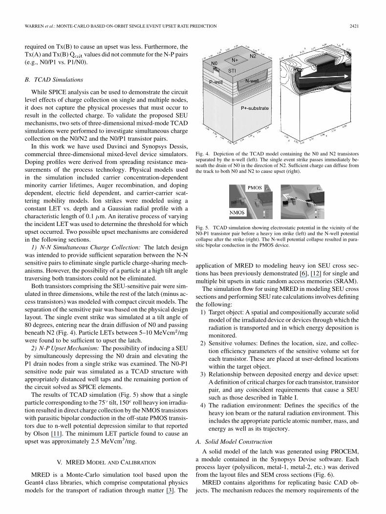
Both transistors comprising the SEU-sensitive pair were sim-ulated in three dimensions, while the rest of the latch (minus ac-cess transistors) was modeled with compact circuit models. Theseparation of the sensitive pair was based on the physical designlayout. The single event strike was simulated at a tilt angle of80 degrees, entering near the drain diffusion of N0 and passingbeneath N2 (Fig. 4). Particle LETs between 5–10 MeVcm /mgwere found to be sufficient to upset the latch.
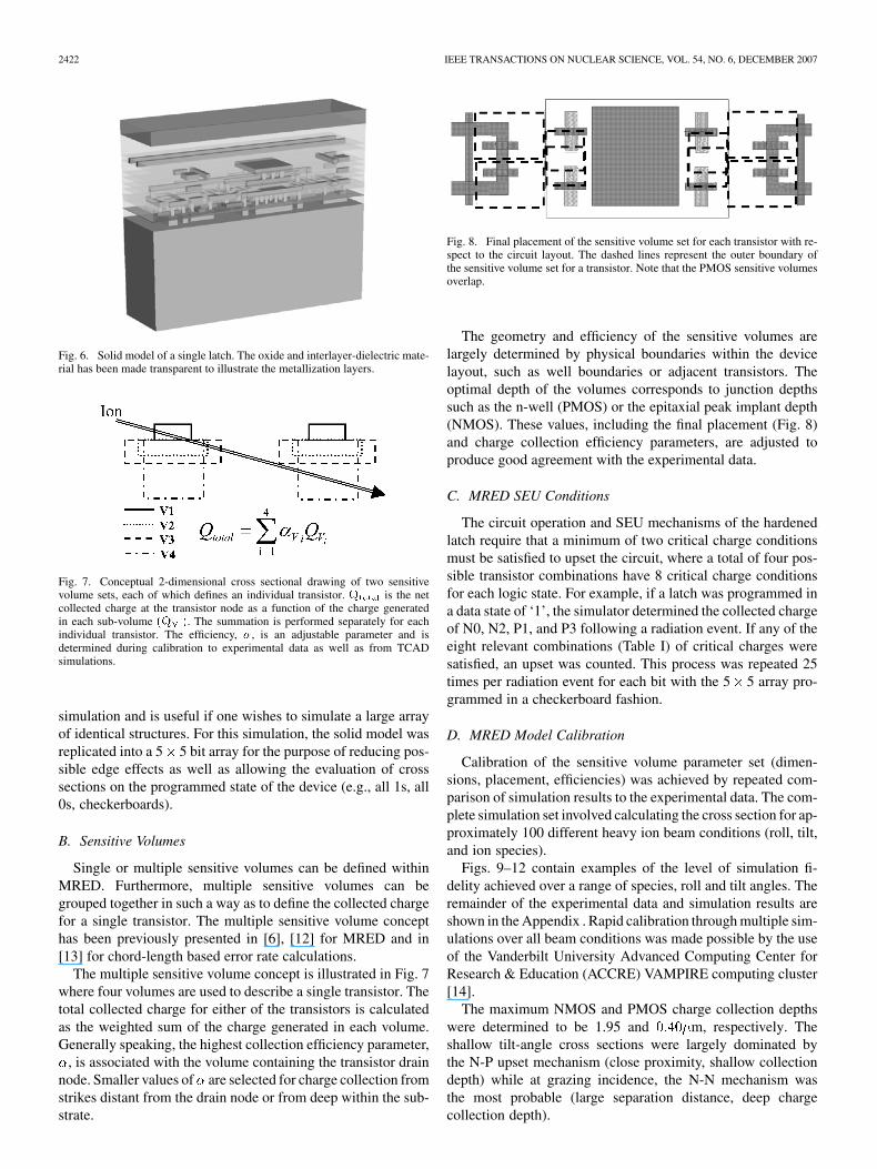
2) N-P Upset Mechanism: The possibility of inducing a SEUby simultaneously depressing the N0 drain and elevating theP1 drain nodes from a single strike was examined. The N0-P1sensitive node pair was simulated as a TCAD structure withappropriately distanced well taps and the remaining portion ofthe circuit solved as SPICE elements.
The results of TCAD simulation (Fig. 5) show that a singleparticle corresponding to the 75 tilt, 150 roll heavy ion irradia-tion resulted in direct charge collection by the NMOS transistorswith parasitic bipolar conduction in the off-state PMOS transis-tors due to n-well potential depression similar to that reportedby Olson [11]. The minimum LET particle found to cause anupset was approximately 2.5 MeVcm /mg.
V. MRED MODEL AND CALIBRATION
MRED is a Monte-Carlo simulation tool based upon theGeant4 class libraries, which comprise computational physicsmodels for the transport of radiation through matter [3]. The
Fig. 4. Depiction of the TCAD model containing the N0 and N2 transistorsseparated by the n-well (left). The single event strike passes immediately be-neath the drain of N0 in the direction of N2. Sufficient charge can diffuse fromthe track to both N0 and N2 to cause upset (right).
Fig. 5. TCAD simulation showing electrostatic potential in the vicinity of theN0-P1 transistor pair before a heavy ion strike (left) and the N-well potentialcollapse after the strike (right). The N-well potential collapse resulted in para-sitic bipolar conduction in the PMOS device.
application of MRED to modeling heavy ion SEU cross sec-tions has been previously demonstrated [6], [12] for single andmultiple bit upsets in static random access memories (SRAM).
The simulation flow for using MRED in modeling SEU crosssections and performing SEU rate calculations involves definingthe following:
1) Target object: A spatial and compositionally accurate solidmodel of the irradiated device or devices through which theradiation is transported and in which energy deposition ismonitored.
2) Sensitive volumes: Defines the location, size, and collec-tion efficiency parameters of the sensitive volume set foreach transistor. These are placed at user-defined locationswithin the target object.
3) Relationship between deposited energy and device upset:A definition of critical charges for each transistor, transistorpair, and any coincident requirements that cause a SEUsuch as those described in Table I.
4) The radiation environment: Defines the specifics of theheavy ion beam or the natural radiation environment. Thisincludes the appropriate particle atomic number, mass, andenergy as well as its trajectory.
A. Solid Model Construction
A solid model of the latch was generated using PROCEM,a module contained in the Synopsys Devise software. Eachprocess layer (polysilicon, metal-1, metal-2, etc.) was derivedfrom the layout files and SEM cross sections (Fig. 6).
MRED contains algorithms for replicating basic CAD ob-jects. The mechanism reduces the memory requirements of the
2422 IEEE TRANSACTIONS ON NUCLEAR SCIENCE, VOL. 54, NO. 6, DECEMBER 2007
Fig. 6. Solid model of a single latch. The oxide and interlayer-dielectric mate-rial has been made transparent to illustrate the metallization layers.
Fig. 7. Conceptual 2-dimensional cross sectional drawing of two sensitivevolume sets, each of which defines an individual transistor. Q is the netcollected charge at the transistor node as a function of the charge generatedin each sub-volume (Q ). The summation is performed separately for eachindividual transistor. The efficiency, �, is an adjustable parameter and isdetermined during calibration to experimental data as well as from TCADsimulations.
simulation and is useful if one wishes to simulate a large arrayof identical structures. For this simulation, the solid model wasreplicated into a 5 5 bit array for the purpose of reducing pos-sible edge effects as well as allowing the evaluation of crosssections on the programmed state of the device (e.g., all 1s, all0s, checkerboards).
B. Sensitive Volumes
Single or multiple sensitive volumes can be defined withinMRED. Furthermore, multiple sensitive volumes can begrouped together in such a way as to define the collected chargefor a single transistor. The multiple sensitive volume concepthas been previously presented in [6], [12] for MRED and in[13] for chord-length based error rate calculations.
The multiple sensitive volume concept is illustrated in Fig. 7where four volumes are used to describe a single transistor. Thetotal collected charge for either of the transistors is calculatedas the weighted sum of the charge generated in each volume.Generally speaking, the highest collection efficiency parameter,
, is associated with the volume containing the transistor drainnode. Smaller values of are selected for charge collection fromstrikes distant from the drain node or from deep within the sub-strate.
Fig. 8. Final placement of the sensitive volume set for each transistor with re-spect to the circuit layout. The dashed lines represent the outer boundary ofthe sensitive volume set for a transistor. Note that the PMOS sensitive volumesoverlap.
The geometry and efficiency of the sensitive volumes arelargely determined by physical boundaries within the devicelayout, such as well boundaries or adjacent transistors. Theoptimal depth of the volumes corresponds to junction depthssuch as the n-well (PMOS) or the epitaxial peak implant depth(NMOS). These values, including the final placement (Fig. 8)and charge collection efficiency parameters, are adjusted toproduce good agreement with the experimental data.
C. MRED SEU Conditions
The circuit operation and SEU mechanisms of the hardenedlatch require that a minimum of two critical charge conditionsmust be satisfied to upset the circuit, where a total of four pos-sible transistor combinations have 8 critical charge conditionsfor each logic state. For example, if a latch was programmed ina data state of ‘1’, the simulator determined the collected chargeof N0, N2, P1, and P3 following a radiation event. If any of theeight relevant combinations (Table I) of critical charges weresatisfied, an upset was counted. This process was repeated 25times per radiation event for each bit with the 5 5 array pro-grammed in a checkerboard fashion.
D. MRED Model Calibration
Calibration of the sensitive volume parameter set (dimen-sions, placement, efficiencies) was achieved by repeated com-parison of simulation results to the experimental data. The com-plete simulation set involved calculating the cross section for ap-proximately 100 different heavy ion beam conditions (roll, tilt,and ion species).
Figs. 9–12 contain examples of the level of simulation fi-delity achieved over a range of species, roll and tilt angles. Theremainder of the experimental data and simulation results areshown in the Appendix . Rapid calibration through multiple sim-ulations over all beam conditions was made possible by the useof the Vanderbilt University Advanced Computing Center forResearch & Education (ACCRE) VAMPIRE computing cluster[14].
The maximum NMOS and PMOS charge collection depthswere determined to be 1.95 and m, respectively. Theshallow tilt-angle cross sections were largely dominated bythe N-P upset mechanism (close proximity, shallow collectiondepth) while at grazing incidence, the N-N mechanism wasthe most probable (large separation distance, deep chargecollection depth).
WARREN et al.: MONTE-CARLO BASED ON-ORBIT SINGLE EVENT UPSET RATE PREDICTION 2423
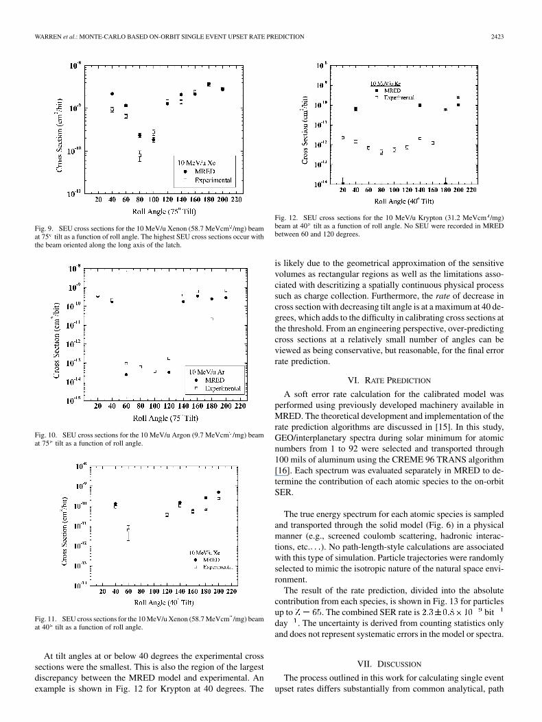
Fig. 9. SEU cross sections for the 10 MeV/u Xenon (58.7 MeVcm /mg) beamat 75 tilt as a function of roll angle. The highest SEU cross sections occur withthe beam oriented along the long axis of the latch.
Fig. 10. SEU cross sections for the 10 MeV/u Argon (9.7 MeVcm /mg) beamat 75 tilt as a function of roll angle.
Fig. 11. SEU cross sections for the 10 MeV/u Xenon (58.7 MeVcm /mg) beamat 40 tilt as a function of roll angle.
At tilt angles at or below 40 degrees the experimental crosssections were the smallest. This is also the region of the largestdiscrepancy between the MRED model and experimental. Anexample is shown in Fig. 12 for Krypton at 40 degrees. The
Fig. 12. SEU cross sections for the 10 MeV/u Krypton (31.2 MeVcm /mg)beam at 40 tilt as a function of roll angle. No SEU were recorded in MREDbetween 60 and 120 degrees.
is likely due to the geometrical approximation of the sensitivevolumes as rectangular regions as well as the limitations asso-ciated with descritizing a spatially continuous physical processsuch as charge collection. Furthermore, the rate of decrease incross section with decreasing tilt angle is at a maximum at 40 de-grees, which adds to the difficulty in calibrating cross sections atthe threshold. From an engineering perspective, over-predictingcross sections at a relatively small number of angles can beviewed as being conservative, but reasonable, for the final errorrate prediction.
VI. RATE PREDICTION
A soft error rate calculation for the calibrated model wasperformed using previously developed machinery available inMRED. The theoretical development and implementation of therate prediction algorithms are discussed in [15]. In this study,GEO/interplanetary spectra during solar minimum for atomicnumbers from 1 to 92 were selected and transported through100 mils of aluminum using the CREME 96 TRANS algorithm[16]. Each spectrum was evaluated separately in MRED to de-termine the contribution of each atomic species to the on-orbitSER.
The true energy spectrum for each atomic species is sampledand transported through the solid model (Fig. 6) in a physicalmanner (e.g., screened coulomb scattering, hadronic interac-tions, etc. ). No path-length-style calculations are associatedwith this type of simulation. Particle trajectories were randomlyselected to mimic the isotropic nature of the natural space envi-ronment.
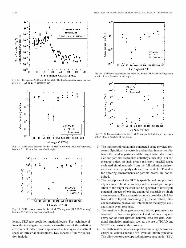
The result of the rate prediction, divided into the absolutecontribution from each species, is shown in Fig. 13 for particlesup to . The combined SER rate is bitday . The uncertainty is derived from counting statistics onlyand does not represent systematic errors in the model or spectra.
VII. DISCUSSION
The process outlined in this work for calculating single eventupset rates differs substantially from common analytical, path
2424 IEEE TRANSACTIONS ON NUCLEAR SCIENCE, VOL. 54, NO. 6, DECEMBER 2007
Fig. 13. Per-species SEU rate of the latch. The final calculated error rate was2:3 + = � 0:8 � 10 errors/bit-day.
Fig. 14. SEU cross sections for the 10 MeV/u Krypton (31.2 MeVcm /mg)beam at 75 tilt as a function of roll angle.
Fig. 15. SEU cross sections for the 10 MeV/u Krypton (31.2 MeVcm /mg)beam at 65 tilt as a function of roll angle.
length, SEU rate prediction methodologies. The technique al-lows the investigator to create a virtualization of the radiationenvironment, either those experienced in testing or in a naturalspace or terrestrial environment. Key aspects of the virtualiza-tion include:
Fig. 16. SEU cross sections for the 10 MeV/u Xenon (58.7 MeVcm /mg) beamat 65 tilt as a function of roll angle.
Fig. 17. SEU cross sections for the 10 MeV/u Argon (9.7 MeV-cm /mg) beamat 65 tilt as a function of roll angle.
1) The transport of radiation is conducted using physical pro-cesses. Specifically, electronic and nuclear interactions be-tween the incident particle and the target material are mod-eled and particles are tracked until they either stop in or exitthe target object. As such, proton and heavy ion SEU can beevaluated simultaneously from the full radiation environ-ment and when properly calibrated, separate DUT modelsfor differing environments or particle beams are not re-quired.
2) The description of the DUT is spatially and composition-ally accurate. The stoichiometry and even isotopic compo-sition of the target material can be specified to investigatepotential impacts of existing and novel materials on singleevent response. The geometric accuracy provides a link be-tween device layout, processing (e.g., metallization, inter-connect density, passivation, interconnect metal type, etc.),and single event response.
3) The sensitive volume geometry and related parameters arecorrelated to transistor placement and calibrated againstheavy ion or other (proton, neutron, etc.) test data. Addi-tional simulation methods, such as the use of TCAD andSPICE, can assist in this process.
4) The mathematical relationship between energy deposition,chargecollection, and valid SEU events is infinitely flexible.Thisallowsone todeveloparadiationresponsemodel (SEU,
WARREN et al.: MONTE-CARLO BASED ON-ORBIT SINGLE EVENT UPSET RATE PREDICTION 2425
SET, etc.) with a level of precision that is adequate for theproblem at hand (e.g., multi-volume charge sharing).
The level of complexity of the SEU response shown in Fig. 3indicates that the concept of effective LET has no reasonablephysical interpretation for devices whose upset response isdriven by multiple node upset mechanisms. SEU cross sectionscannot be viewed as single critical charge and simple pathlength calculation in a single rectangular volume. Rather, onemust consider the charge characteristics of multiple transistorsand the probabilities of coincident charge collection dominatingthe SEU response.
VIII. CONCLUSION
The latch design eliminates single node charge collection SEUvulnerabilities but is susceptible to multiple node charge collec-tion processes. Specifically, charge collection from depths up to2.0 m within the substrate in NMOS transistors and parasiticbipolar action in the PMOS transistors increase the probabilityof a single particle affecting multiple nodes. While physical sep-aration of the NMOS transistors reduces the probability of N-Nupsets, it is not completely eliminated for grazing incidence par-ticles. Furthermore, improved means of isolating sensitive N-Ppairs are required to improve SEU immunity.
The agreement between the model and the experimental datafor the hardened latch not only supports the proposed mechanismand the simulation methodology, but also provides the maximumpossible confidence in the final on-orbit soft error rate prediction.
In applications where extensive resources have been used todevelop SEU immune or resistant storage elements, the on-orbitsoft error rate is inherently a critical metric of the device’s per-formance. However, as has been demonstrated, SEU hardeneddevices’ cross sections and their error rates can be dominated bysecond order mechanisms that fall outside of the applicabilityof the classical single-volume RPP models. The flexibility ofMRED (or potentially other suitably developed physics-basedtransport codes) allows one to overcome these limitations andhelps to reduce the systematic uncertainty associated with theon-orbit error rate prediction process. Insight into the SEUmechanisms, both in the context of their relative contribution toheavy ion cross sections and the predicted SEU rate, providesvaluable feedback to circuit and layout engineers to assist inimproving the overall SEU immunity.
APPENDIX
Figs. 14, 15, 16, and 17 contain the remainder of the heavy iondata and the corresponding calibrated simulation results. Thebest visual agreement between experiment and simulation wasachieved at the large tilt angles. As the tilt angle was reduced, ex-perimentally measured SEU cross sections decreased substan-tially. The point at which the rate of decrease in cross sectionwith respect to tilt angle was greatest represents that area withthe greatest discrepancy between experiment and simulation.
REFERENCES
[1] J. D. Black, A. L. Sternberg, M. L. Alles, A. F. Witulski, B. L. Bhuva, L.W. Massengill, J. M. Benedetto, M. P. Baze, J. W. Wert, and M. G. Hu-bert, “HBD layout isolation techniques for multiple node charge collec-tion mitigation,” IEEE Trans. Nucl. Sci., vol. 52, no. 6, pp. 2536–2541,Dec. 2005.
[2] L. W. Connell and F. W. Sexton, “Further development of the heavyion cross section for single event upset: Model (HICUP),” IEEE Trans.Nucl. Sci., vol. 42, no. 6, pp. 2026–2034, Dec. 1995.
[3] C. Inguimbert and S. Duzellier, “SEU rate calculation with Geant4(comparison with CRÈME 86),” IEEE Trans. Nucl. Sci., vol. 51, no.5, pp. 2805–2810, Oct. 2004.
[4] D. Lambert, J. Baggio, V. Ferlet-Cavrois, O. Flament, F. Saigne, B.Sagnes, N. Buard, and T. Carriere, “Neutron-induced SEU in bulkSRAMs in terrestrial environment: Simulations and experiments,”IEEE Trans. Nucl. Sci., vol. 51, no. 6, pp. 3435–3441, Dec. 2004.
[5] C. L. Howe, R. A. Weller, R. A. Reed, M. H. Mendenhall, R. D.Schrimpf, K. M. Warren, D. R. Ball, L. W. Massengill, K. A. LaBel, J.W. Howard, and N. F. Haddad, “Role of heavy-ion nuclear reactionsin determining on-orbit single event error rates,” IEEE Trans. Nucl.Sci., vol. 52, no. 6, pp. 2182–2188, Dec. 2005.
[6] K. M. Warren, B. D. Sierawski, R. A. Weller, R. A. Reed, M. H.Mendenhall, J. A. Pellish, R. D. Schrimpf, L. W. Massengill, M. E.Porter, and J. W. Wilkinson, “Predicting thermal neutron-inducedsoft errors in static memories using TCAD and physics-based montecarlo simulation tools,” IEEE Electron Device Lett., vol. 28, no. 2, pp.180–182, Feb. 2007.
[7] S. Agostinelli, J. Allison, K. Amako, J. Apostolakis, H. Araujo, P.Arce, M. Asai, D. Axen, S. Banerjee, G. Barrand, F. Behner, L.Bellagamba, J. Boudreau, L. Broglia, A. Brunengo, H. Burkhardt,S. Chauvie, J. Chuma, R. Chytracek, G. Cooperman, G. Cosmo, P.Degtyarenko, A. Dell’Acqua, G. Depaola, D. Dietrich, R. Enami,A. Feliciello, C. Ferguson, H. Fesefeldt, G. Folger, F. Foppiano, A.Forti, S. Garelli, S. Giani, R. Giannitrapani, D. Gibin, J. J. Gomez,C. Cadenas, I. Gonzalez, G. Gracia Abril, G. Greeniaus, W. Greiner,V. Grichine, A. Grossheim, S. Guatelli, P. Gumplinger, R. Hamatsu,K. Hashimoto, H. Hasui, A. Heikkinen, A. Howard, V. Ivanchenko,A. Johnson, F. W. Jones, J. Kallenbach, N. Kanaya, M. Kawabata, Y.Kawabata, M. Kawaguti, S. Kelner, P. Kent, A. Kimura, T. Kodama,R. Kokoulin, M. Kossov, H. Kurashige, E. Lamanna, T. Lampen,V. Lara, V. Lefebure, F. Lei, M. Liendl, W. Lockman, F. Longo, S.Magni, M. Maire, E. Medernach, K. Minamimoto, P. Mora de Freitas,Y. Morita, K. Murakami, M. Nagamatu, R. Nartallo, P. Nieminen,T. Nishimura, K. Ohtsubo, M. Okamura, S. O’Neale, Y. Oohata, K.Paech, J. Perl, A. Pfeiffer, M. G. Pia, F. Ranjard, A. Rybin, S. Sadilov,E. Di Salvo, G. Santin, T. Sasaki, N. Savvas, Y. Sawada, S. Scherer, S.Sei, V. Sirotenko, D. Smith, N. Starkov, H. Stoecker, J. Sulkimo, M.Takahata, S. Tanaka, E. Tcherniaev, E. Safai Tehrani, M. Tropeano,P. Truscott, H. Uno, L. Urban, P. Urban, M. Verderi, A. Walkden,W. Wander, H. Weber, J. P. Wellisch, T. Wenaus, D. C. Williams,D. Wright, T. Yamada, H. Yoshida, and D. Zschiesche, “Geant4-asimulation toolkit,” Nucl. Instrum. Methods Phys. Res. A, vol. A506,p. 250, 2003.
[8] [Online]. Available: http://www.python.org[9] T. Calin, M. Nicolaidis, and R. Velazco, “Upset hardened memory de-
sign for submicron CMOS technology,” IEEE Trans. Nucl. Sci., vol.43, no. 6, pp. 2874–2878, Dec. 1996.
[10] R. Velazco, T. Calin, M. Nicolaidis, S. C. Moss, S. D. LaLumonDiere,V. T. Tran, and R. Koga, “SEU-hardened storage cell validation usinga pulsed laser,” IEEE Trans. Nucl. Sci., vol. 43, no. 6, pp. 2843–2848,Dec. 1996.
[11] B. D. Olson, D. R. Ball, K. M. Warren, L. W. Massengill, N. F. Haddad,S. E. Doyle, and D. McMorrow, “Simultaneous single event chargesharing and parasitic bipolar conduction in a highly-scaled SRAM de-sign,” IEEE Trans. Nucl. Sci., vol. 52, no. 6, pp. 2132–2136, Dec. 2005.
[12] K. M. Warren, R. A. Weller, B. Sierawski, R. A. Reed, M. H. Menden-hall, R. D. Schrimpf, L. W. Massengill, M. Porter, J. Wilkinson, K.A. LaBel, and J. Adams, “Application of RADSAFE to model singleevent upset response of a 0.25 micron CMOS SRAM,” IEEE Trans.Nucl. Sci., accepted for publication.
[13] D. E. Fulkerson, D. K. Nelson, and R. M. Carlson, “BOXES: An engi-neering methodology for calculating soft error rates in SOI integratedcircuit,” IEEE Trans. Nucl. Sci., vol. 53, no. 6, pp. 3329–3335, Dec.2007.
[14] [Online]. Available: http://www.accre.vanderbilt.edu[15] R. A. Reed, R. A. Weller, R. D. Schrimpf, M. H. Mendenhall, K. M.
Warren, and L. W. Massengill, “Implications of nuclear reactions forsingle event effects test methods and analysis,” IEEE Trans. Nucl. Sci.,vol. 53, no. 6, pp. 3356–3362, Dec. 2007.
[16] A. J. Tylka, J. H. Adams, J. P. R. Boberg, B. Brownstein, W. F. Dietrich,E. O. Flueckiger, E. L. Petersen, M. A. Shea, D. F. Smart, and E. C.Smith, “CREME 96: A revision of the cosmic ray effects on micro-electronics code,” IEEE Trans. Nucl. Sci., vol. 44, no. 6, pp. 2150–2160,Dec. 1997.
Related Documents