MonolithIC 3D Inc. Patents Pending 1 THE MONOLITHIC 3D-IC A DISRUPTOR TO THE SEMICONDUCTOR INDUSTRY

Welcome message from author
This document is posted to help you gain knowledge. Please leave a comment to let me know what you think about it! Share it to your friends and learn new things together.
Transcript
MonolithIC 3D Inc. Patents Pending 1
THE MONOLITHIC 3D-IC
A DISRUPTOR TO THE SEMICONDUCTOR INDUSTRY

Agenda:
The Semiconductor future is exciting
But we are reaching an inflection point
Monolithic 3D IC – the emerging path for the next generation technology driver
The challenge and solution for the fabrication of monolithic 3D IC
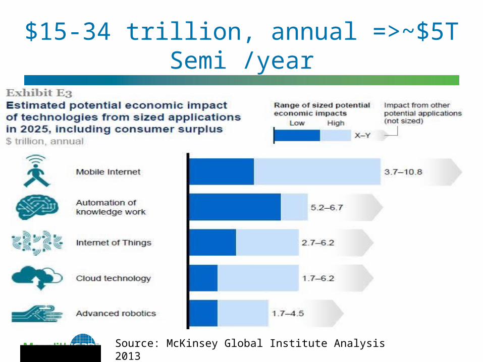
$15-34 trillion, annual =>~$5T Semi /year
Source: McKinsey Global Institute Analysis 2013

Cisco sees $19 Trillion opportunity in IoT
“CES LIVE: Cisco's Chambers Says Internet of Everything, $19 Trillion Opportunity, Is Next Big Thing” 1/7/14<ttp://www.forbes.com/sites/connieguglielmo/2014/01/07/ces-live-cisco-ceo-chambers-to-deliver-keynote/>
$19 trillion: that’s the opportunity he says for the Internet of Everything in the private and public sector combined. Breakout is $14.4 trillion in private sector and $4.6 trillion in public sector of new revenue generation or new savings. That’s a conservative number he says for public sector.
“This will be bigger than anything done in high tech in a decade.”
“As many as 50 billion devices will be connected to the Internet by 2020, creating a $14.4 trillion business opportunity” said Rob Lloyd, president of sales and development at Cisco, <http://www.eetimes.com/electronics-news/4409928/Cisco-sees--14-trillion-opportunity-in-Internet-of-Things>
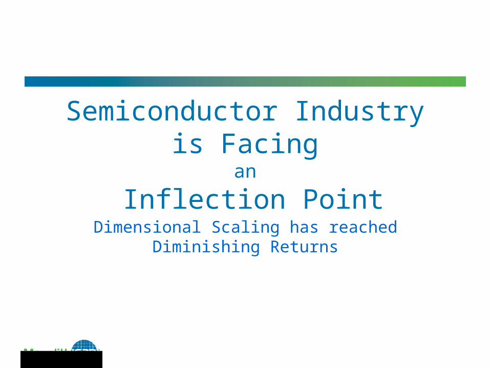
Semiconductor Industry is Facingan
Inflection Point
Dimensional Scaling has reached Diminishing Returns
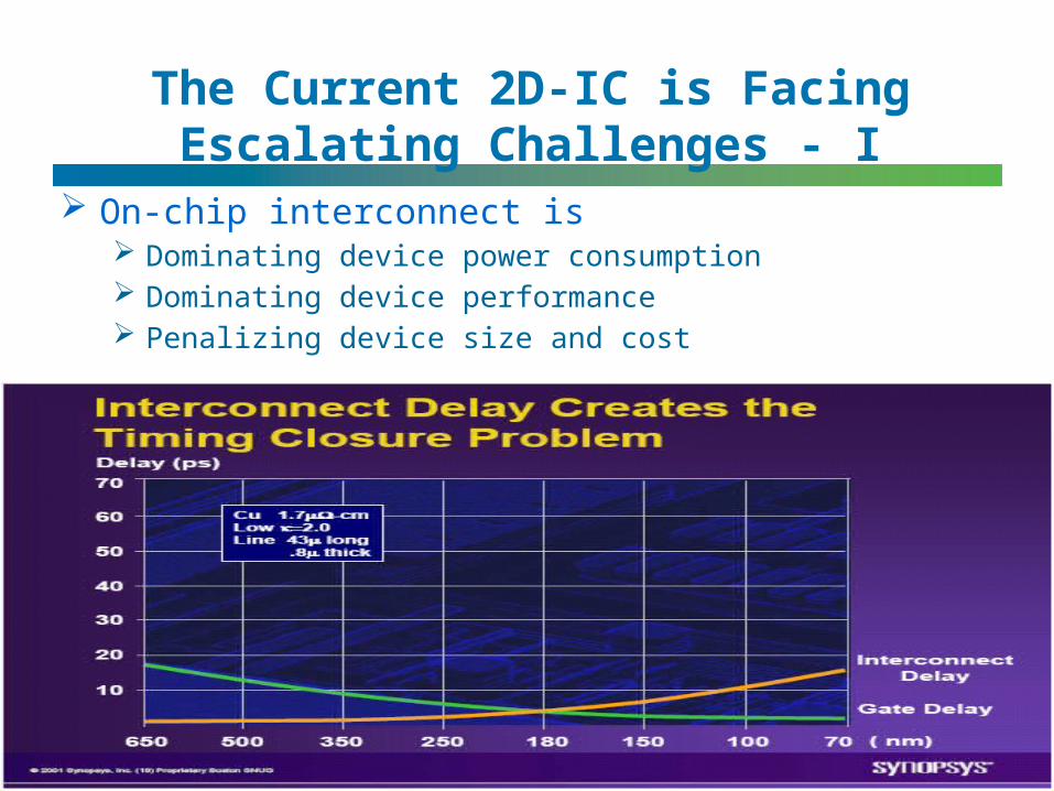
The Current 2D-IC is Facing Escalating Challenges - I
On-chip interconnect is Dominating device power consumption Dominating device performance Penalizing device size and cost
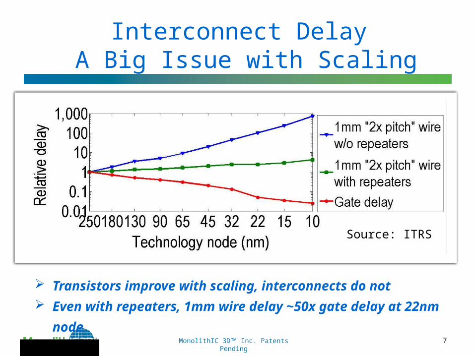
Interconnect Delay A Big Issue with Scaling
MonolithIC 3D Inc. Patents Pending 7
Transistors improve with scaling, interconnects do not Even with repeaters, 1mm wire delay ~50x gate delay at 22nm node
Source: ITRS
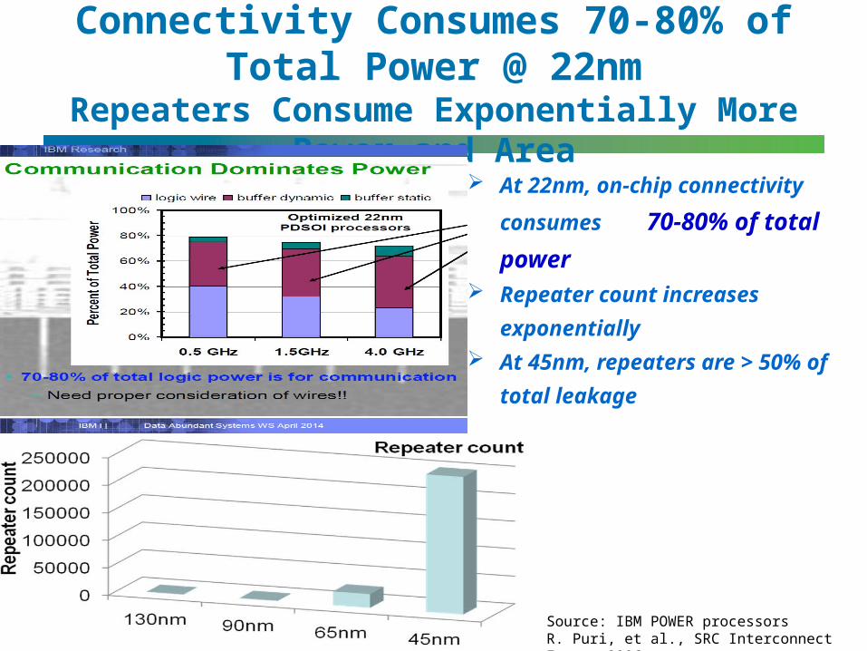
Connectivity Consumes 70-80% of Total Power @ 22nmRepeaters Consume Exponentially More Power and Area
MonolithIC 3D Inc. Patents Pending Source: IBM POWER processorsR. Puri, et al., SRC Interconnect Forum, 2006
At 22nm, on-chip connectivity consumes
70-80% of total power Repeater count increases exponentially At 45nm, repeaters are > 50% of total
leakage
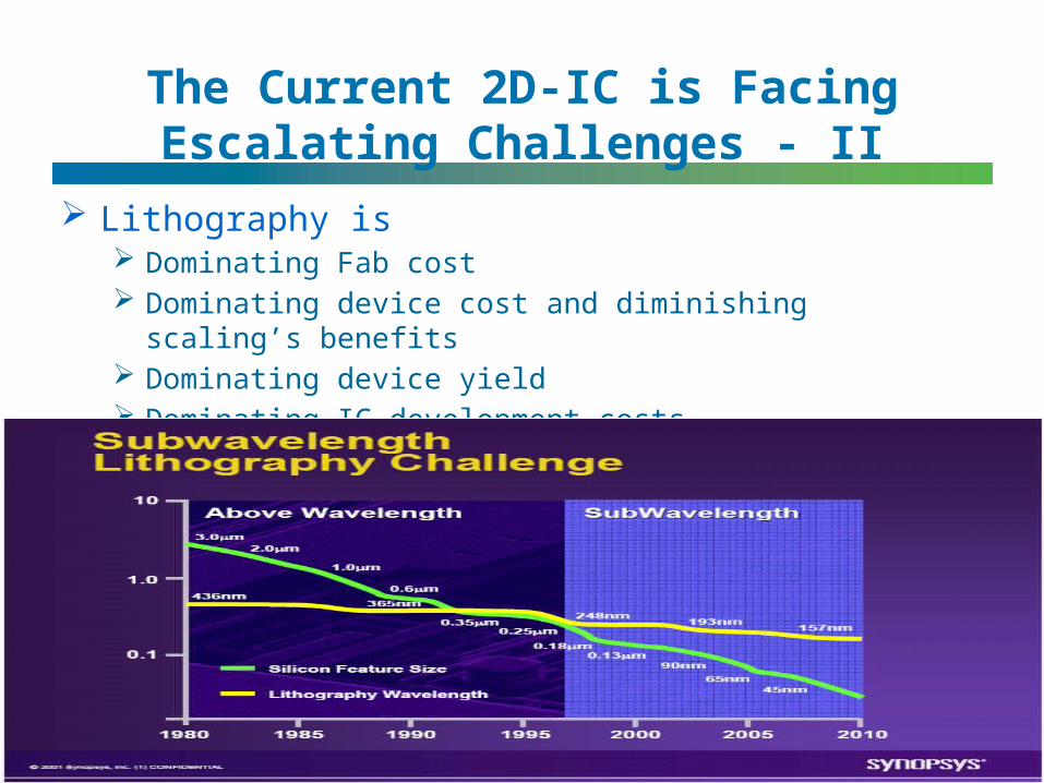
The Current 2D-IC is Facing Escalating Challenges - II
Lithography is Dominating Fab cost Dominating device cost and diminishing scaling’s
benefits Dominating device yield Dominating IC development costs

A Challenge: Lithography
Quad-patterning next year costly. EUV delayed, costly.
Can we get benefits of scaling without relying on
lithography?MonolithIC 3D Inc. Patents Pending 10

Martin van den Brink -EVP & CTO, ASMLISSCC 2013 & SemiconWest 2013
Dinesh Maheshwari, CTO, Memory Products Division at Cypress Semiconductors, ISSCC2014
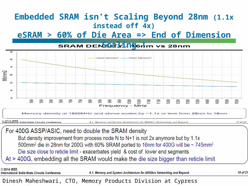
Embedded SRAM isn’t Scaling Beyond 28nm (1.1x instead off 4x)
eSRAM > 60% of Die Area => End of Dimension Scaling !
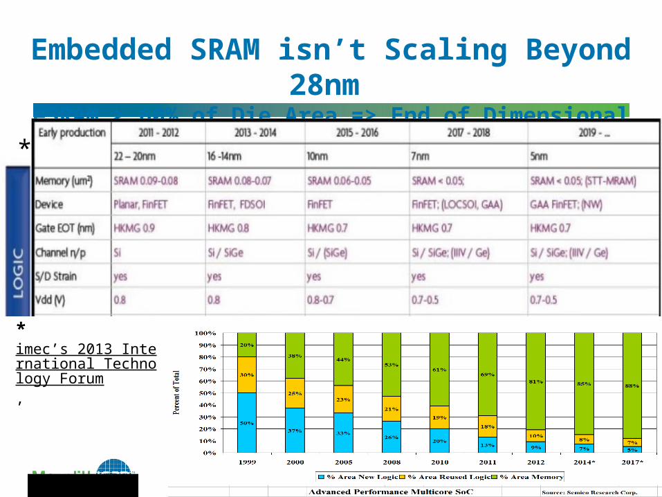
Embedded SRAM isn’t Scaling Beyond 28nm eSRAM > 60% of Die Area => End of Dimensional Scaling !
*
*imec’s 2013 International Technology Forum,
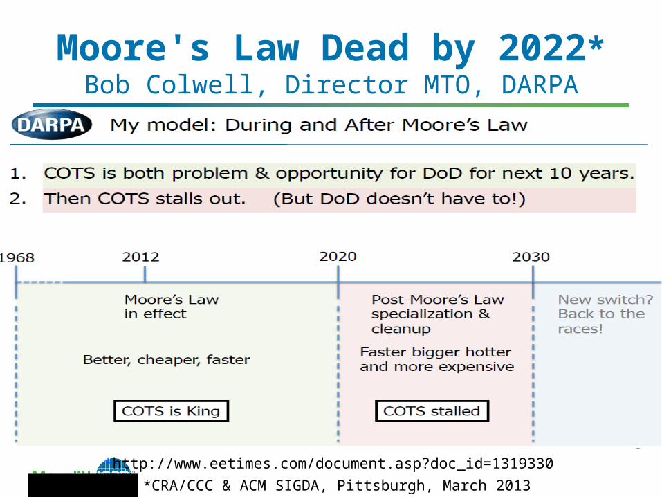
Moore's Law Dead by 2022*Bob Colwell, Director MTO, DARPA
*CRA/CCC & ACM SIGDA, Pittsburgh, March 2013
*http://www.eetimes.com/document.asp?doc_id=1319330

Conclusions:
Dimensional Scaling (“Moore’s Law”) is already exhibiting diminishing returns
The road map beyond 2017 (7nm) is unclear While the research community is working on many interesting
new technologies (see below), none of them seem mature enough to replace silicon for 2019
- Carbon nanotube - Indium gallium arsenide -’2D’ devices: MoS2, etc
- Graphene - Spintronics
- Nanowire - Molecular computing
- Photonics - Quantum computing
3D IC is considered, by all, as the near term solution, and Monolithic 3D IC is well positioned to be so, as it uses the existing infrastructure It is safe to state that Monolithic 3D is the only alternative
that could be ready for high volume in 2019

CMOS is the Best Device Option

3D and EDA need to make up for Moore’s Law, says Qualcomm*
“Qualcomm is looking to monolithic 3D and smart circuit architectures to make up for the loss of traditional 2D process scaling as wafer costs for advanced nodes continue to increase. .. Now, although we are still scaling down it’s not cost-economic anymore”
“Interconnect RC is inching up as we go to deeper technology. That is a major problem because designs are becoming interconnect-dominated. Something has to be done about interconnect. What needs to be done is monolithic three-dimensional ICs.”
“TSV...are not really solving the interconnect issue I’m talking about.So we are looking at true monolithic 3D. You have normal vias between different stacks.”
* Karim Arabi Qualcomm VP of engineering Key Note
DAC 2014<http://www.techdesignforums.com/blog/2014/06/05/karim-arabi-monolithic-
3dic-dac-2014/>

“CEA-Leti Signs Agreement with Qualcomm to Assess Sequential (monolithic)3D Technology”Business Wire December 08, 2013
“Monolithic 3D (M3D) is an emerging integration technology poised to reduce the gap significantly between transistors and interconnect delays to extend the semiconductor roadmap way beyond the 2D scaling trajectory predicted by Moore’s Law.”
Geoffrey Yeap, VP of Technology at Qualcomm, Invited paper, IEDM 2013


Two Types of 3D Technology
21
3D-TSVTransistors made on separate
wafer @ high temperature, then thin + align + bond
TSV pitch > 1um*
Monolithic 3DTransistors made monolithically
atop wiring (@ sub-400oC for logic)
TSV pitch ~ 50-100nm
10um-50um
100 nm
* [Reference: P. Franzon: Tutorial at IEEE 3D-IC Conference 2011]
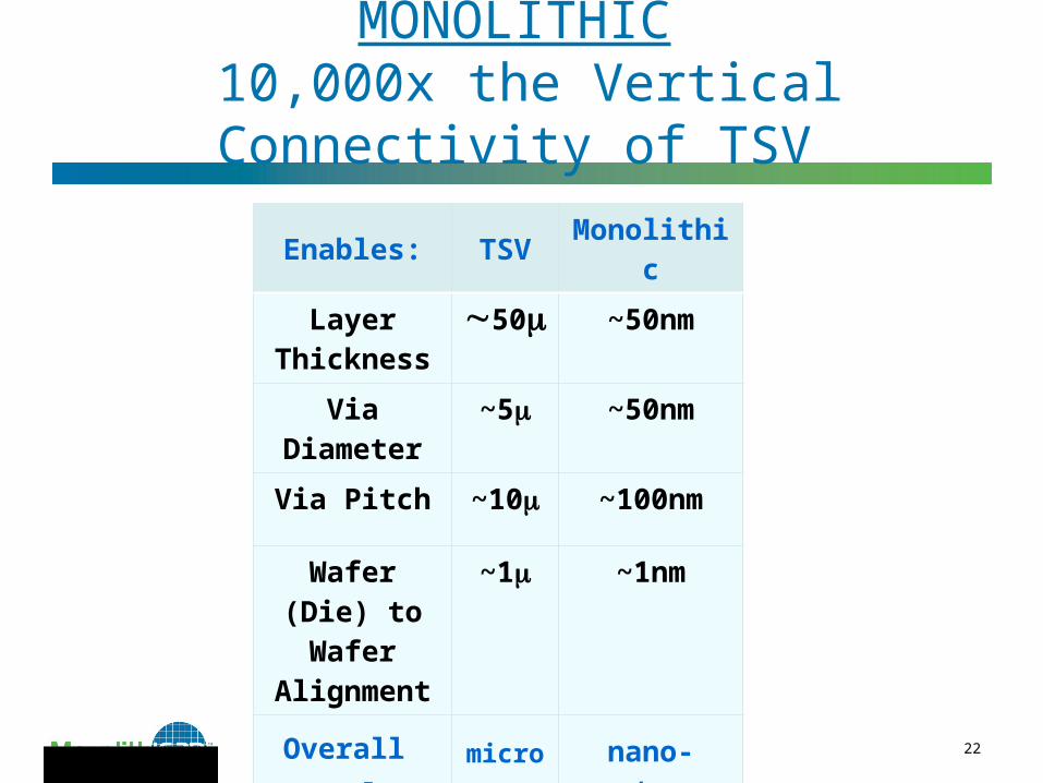
MonolithIC 3D Inc. Patents Pending 22
Enables: TSV Monolithic
Layer Thickness
~50m
~50nm
Via Diameter ~5m ~50nm
Via Pitch ~10m ~100nm
Wafer (Die) to Wafer
Alignment
~1m ~1nm
Overall Scale
microns nano-meters
MONOLITHIC 10,000x the Vertical Connectivity of TSV

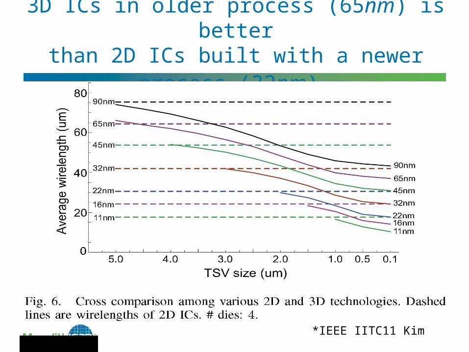
3D ICs in older process (65nm) is betterthan 2D ICs built with a newer process (32nm)
*IEEE IITC11 Kim


MonolithIC 3D Inc. Patents Pending 26
Processing on top of copper interconnects should not make the copper interconnect exceed 400oC
How to bring mono-crystallized silicon on top at less than 400oC How to fabricate state-of-the-art transistors on top of copper interconnect
and keep the interconnect below at less than 400oC
Misalignment of pre-processed wafer to wafer bonding step is ~1um
How to achieve 100nm or better connection pitch How to fabricate thin enough layer for inter-layer vias of ~50nm
The Monolithic 3D ChallengeWhy is it not already in wide use?
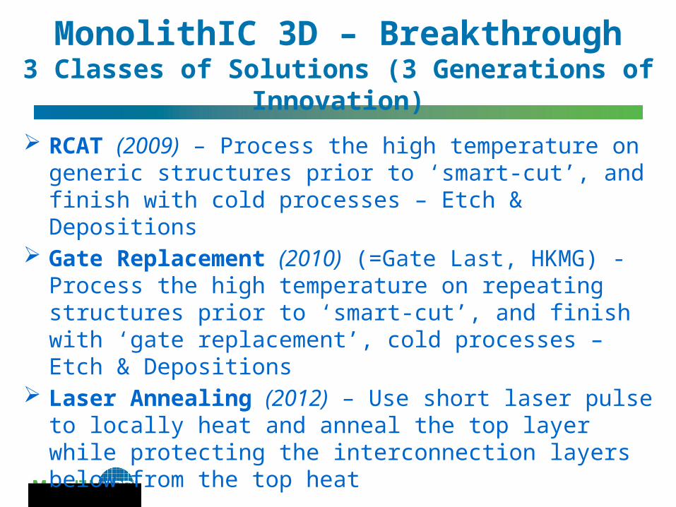
MonolithIC 3D – Breakthrough3 Classes of Solutions (3 Generations of Innovation)
RCAT (2009) – Process the high temperature on generic structures prior to ‘smart-cut’, and finish with cold processes – Etch & Depositions
Gate Replacement (2010) (=Gate Last, HKMG) - Process the high temperature on repeating structures prior to ‘smart-cut’, and finish with ‘gate replacement’, cold processes – Etch & Depositions
Laser Annealing (2012) – Use short laser pulse to locally heat and anneal the top layer while protecting the interconnection layers below from the top heat
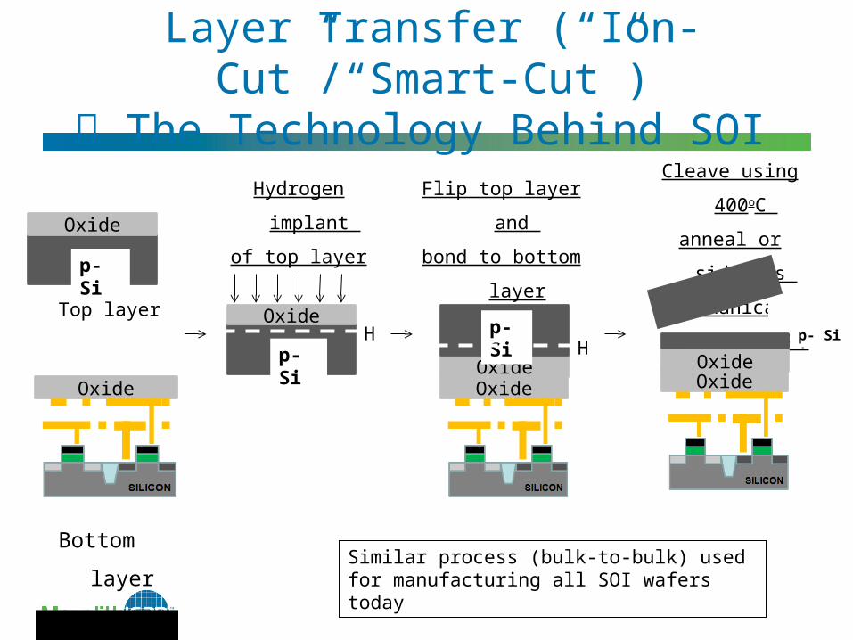
Layer Transfer (“Ion-Cut”/“Smart-Cut”) The Technology Behind SOI
p- Si
Oxide
p- Si
OxideH
Top layer
Bottom layer
Oxide
Hydrogen implant
of top layer
Flip top layer and
bond to bottom layer
Oxide
p- Si
Oxide
H
Cleave using 400oC
anneal or sideways
mechanical force. CMP.
OxideOxide
Similar process (bulk-to-bulk) used for manufacturing all SOI wafers today
p- Si

MonolithIC 3D - 3 Classes of Solutions
RCAT – Process the high temperature on generic structure prior to ‘smart-cut’, and finish with cold processes – Etch & Depositions
Gate Replacement (=Gate Last, HKMG) - Process the high temperature on repeating structure prior to ‘smart-cut’, and finish with ‘gate replacement’, cold processes – Etch & Depositions
Laser Annealing – Use short laser pulse to locally heat and anneal the top layer while protecting the interconnection layers below from the top heat

MonolithIC 3D Inc. Patents Pending 30
Step 1 - Implant and activate unpatterned N+ and P- layer regions in standard donor wafer at high temp. (~900oC) before layer transfer. Oxidize (or CVD oxide)
top surface.
Step 1. Donor Layer Processing
Step 2 - Implant H+ to form cleave plane for the ion cut
N+P-
P-
SiO2 Oxide layer (~100nm) for oxide -to-oxide bonding with device wafer.
N+P-
P-
H+ Implant Cleave Line in N+ or below
MonolithIC 3D Inc. Patents Pending 31
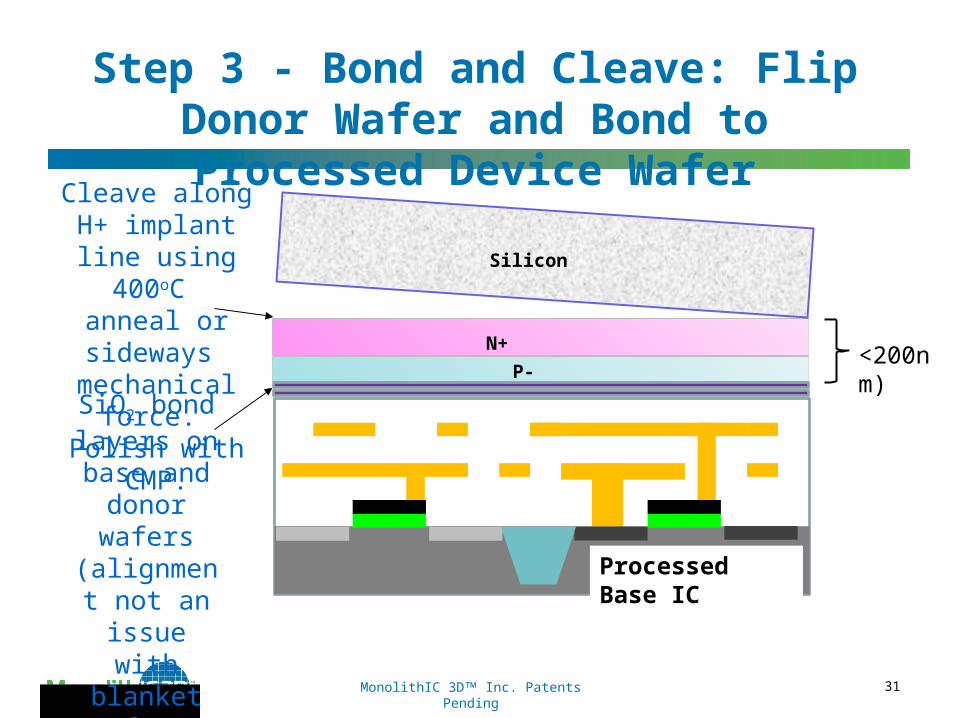
Step 3 - Bond and Cleave: Flip Donor Wafer and Bond to Processed Device Wafer
Cleave alongH+ implant line using 400oC
anneal or sideways mechanical force. Polish with CMP.
-
N+
P-
Silicon
SiO2 bond layers on base
and donor wafers
(alignment not an issue with
blanket wafers)
<200nm)
Processed Base IC
MonolithIC 3D Inc. Patents Pending 32
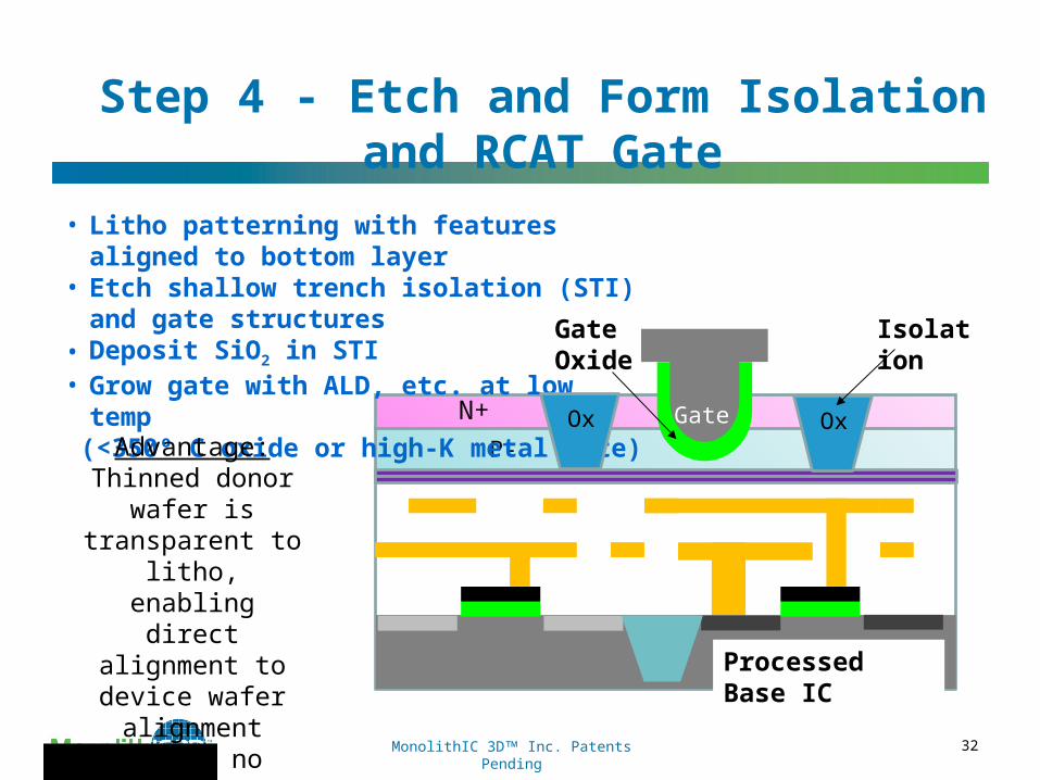
Step 4 - Etch and Form Isolation and RCAT Gate
+N
P-
GateOxide
Isolation
• Litho patterning with features aligned to bottom layer• Etch shallow trench isolation (STI) and gate structures• Deposit SiO2 in STI• Grow gate with ALD, etc. at low temp (<350º C oxide or high-K metal gate)
Ox Ox
Gate
Advantage: Thinned donor wafer is
transparent to litho, enabling direct
alignment to device wafer alignment marks: no indirect alignment. (common for TSV 3DIC) Processed Base IC
MonolithIC 3D Inc. Patents Pending 33
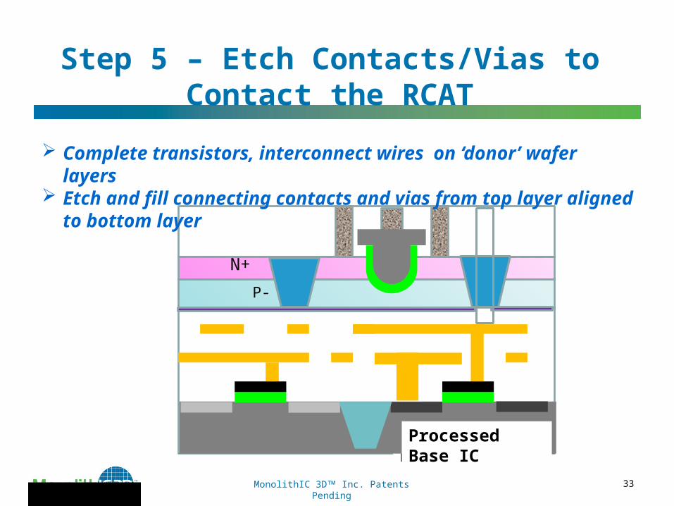
Step 5 – Etch Contacts/Vias to Contact the RCAT
+N
P-
Processed Base IC
Complete transistors, interconnect wires on ‘donor’ wafer layers Etch and fill connecting contacts and vias from top layer aligned to bottom
layer
Processed Base IC

MonolithIC 3D - 3 Classes of Solutions
RCAT – Process the high temperature on generic structure prior to ‘smart-cut’, and finish with cold processes – Etch & Depositions
Gate Replacement (=Gate Last, HKMG) - Process the high temperature on repeating structure prior to ‘smart-cut’, and finish with ‘gate replacement’, cold processes – Etch & Depositions
Laser Annealing – Use short laser pulse to locally heat and anneal the top layer while protecting the interconnection layers below from the top heat

MonolithIC 3D Inc. Patents Pending 35
Fully constructed transistors attached to each other; no blanket films
proprietary methods align top layer atop bottom layer
Device wafer
Donor wafer
A Gate-Last Process for Cleave and Layer Transfer
NMOS PMOS PolyOxide

MonolithIC 3D Inc. Patents Pending 36
Step 3. Implant H for cleaving
Step 4. Bond to temporary carrier wafer
(adhesive or oxide-to-oxide) Cleave along cut line CMP to STI
H+ Implant Cleave Line
CMP to STI
A Gate-Last Process for Cleave and Layer Transfer
NMOS PMOS
Carrier
STI
MonolithIC 3D Inc. Patents Pending 37
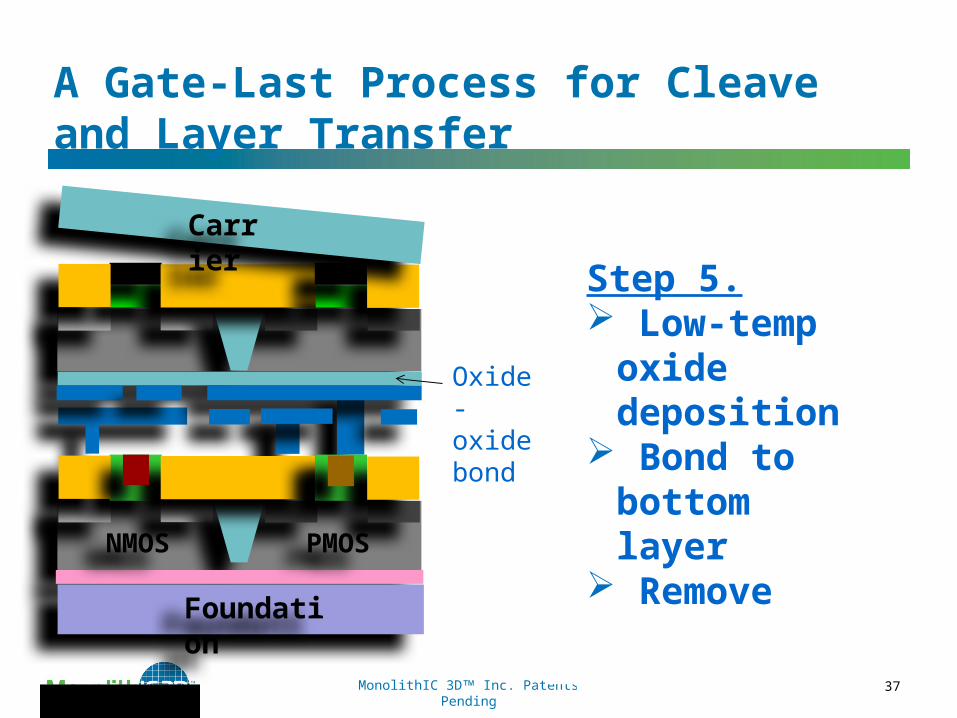
Step 5. Low-temp oxide
deposition Bond to bottom
layer Remove carrier
Oxide-oxide bond
A Gate-Last Process for Cleave and Layer Transfer
Foundation
Carrier
NMOS PMOS

MonolithIC 3D Inc. Patents Pending 38
Step 6. On transferred layer: Etch dummy gates Deposit gate dielectric and
electrode CMP Etch tier-to-tier vias thru STI Fabricate BEOL interconnect
Remove (etch) dummy gates, replace with HKMG
A Gate-Last Process for Cleave and Layer Transfer
NMOS PMOS
NMOS PMOS
MonolithIC 3D Inc. Patents Pending 39
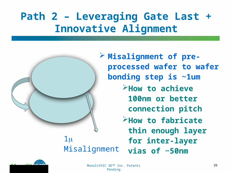
Path 2 – Leveraging Gate Last + Innovative Alignment
Misalignment of pre-processed wafer to wafer bonding step is ~1um
How to achieve 100nm or better connection pitch
How to fabricate thin enough layer for inter-layer vias of ~50nm
1 mMisalignment
MonolithIC 3D Inc. Patents Pending 40
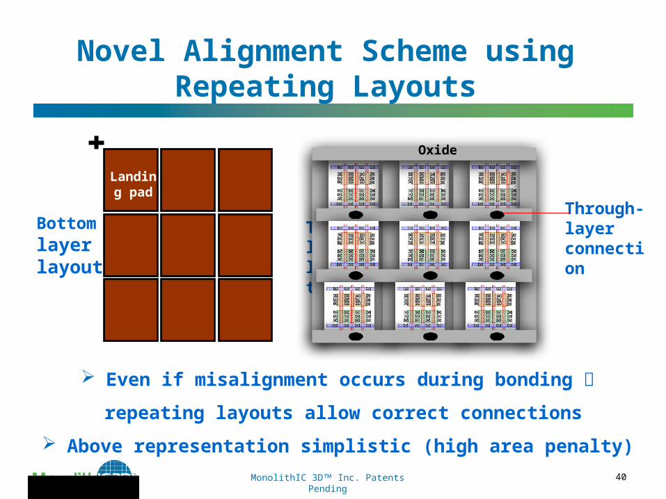
Novel Alignment Scheme using Repeating Layouts
Even if misalignment occurs during bonding
repeating layouts allow correct connections
Above representation simplistic (high area penalty)
Bottom layerlayout
Top layerlayout
Landing pad
Through-layer connection
Oxide
MonolithIC 3D Inc. Patents Pending 41
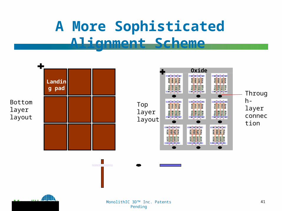
A More Sophisticated Alignment Scheme
Bottom layerlayout
Top layerlayout
Landing pad
Through-layer connection
Oxide
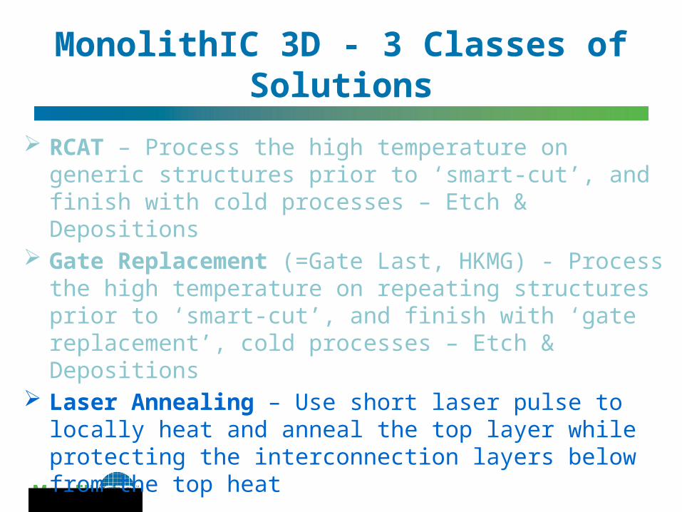
MonolithIC 3D - 3 Classes of Solutions
RCAT – Process the high temperature on generic structures prior to ‘smart-cut’, and finish with cold processes – Etch & Depositions
Gate Replacement (=Gate Last, HKMG) - Process the high temperature on repeating structures prior to ‘smart-cut’, and finish with ‘gate replacement’, cold processes – Etch & Depositions
Laser Annealing – Use short laser pulse to locally heat and anneal the top layer while protecting the interconnection layers below from the top heat

Annealing Trend with Scaling

LSA 100A – Short Pulse, Small Spot
Dwell time ~ 275µs
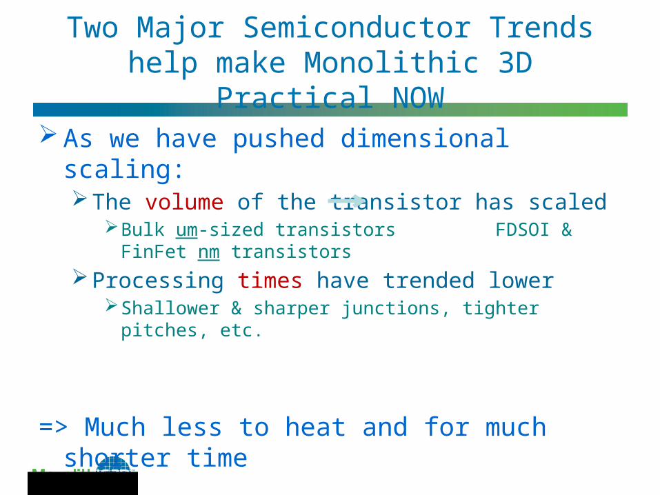
Two Major Semiconductor Trends help make Monolithic 3D Practical NOW
As we have pushed dimensional scaling:The volume of the transistor has scaled
Bulk um-sized transistors FDSOI & FinFet nm transistors
Processing times have trended lowerShallower & sharper junctions, tighter pitches, etc.
=> Much less to heat and for much shorter time
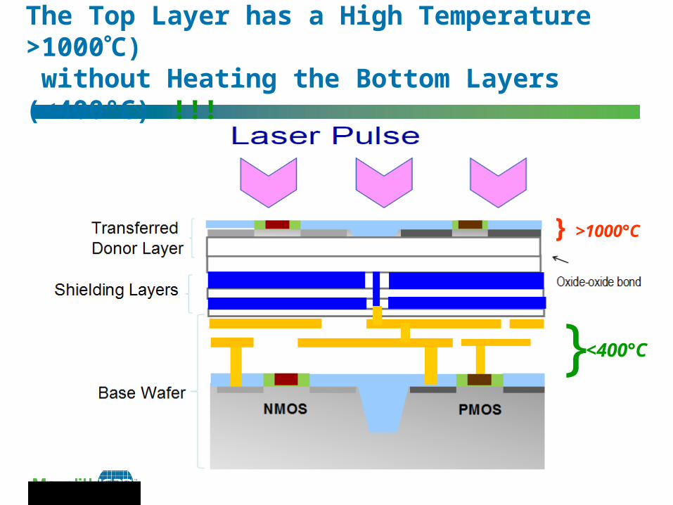
The Top Layer has a High Temperature >1000C) without Heating the Bottom Layers (<400°C) !!!
>1000°C
<400°C}
}

Process Window Set to Avoid Damage
Temperature variation at the 20 nm thick Si source/drain region in the upper active layer during laser annealing. Note that the shield layers are very effective in preventing any large thermal excursions in the lower layers
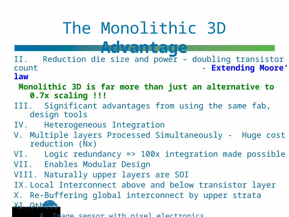
II. Reduction die size and power – doubling transistor count - Extending Moore’s law Monolithic 3D is far more than just an alternative to 0.7x
scaling !!!III. Significant advantages from using the same fab, design toolsIV. Heterogeneous IntegrationV. Multiple layers Processed Simultaneously - Huge cost reduction
(Nx) VI. Logic redundancy => 100x integration made possibleVII. Enables Modular DesignVIII.Naturally upper layers are SOIIX. Local Interconnect above and below transistor layerX. Re-Buffering global interconnect by upper strataXI. Others
A. Image sensor with pixel electronics B. Micro-display
The Monolithic 3D Advantage

Monolithic 3D Provides an Attractive Path to…
3D-CMOS: Monolithic 3D Logic Technology
3D-FPGA: Monolithic 3D Programmable Logic
3D-GateArray: Monolithic 3D Gate Array
3D-Repair: Yield recovery for high-density chips
3D-DRAM: Monolithic 3D DRAM
3D-RRAM: Monolithic 3D RRAM
3D-Flash: Monolithic 3D Flash Memory
3D-Imagers: Monolithic 3D Image Sensor
3D-MicroDisplay: Monolithic 3D Display
3D-LED: Monolithic 3D LED
Monolithic 3D Integration with Ion-
Cut Technology
Can be applied to many market
segments
LOGIC
MEMORY
OPTO-ELECTRONICS
MonolithIC 3D Inc. Patents Pending 50

Summary
Monolithic 3D is now practical and well positioned to keep Moore’s Law alive for many years
Multiple paths to process mono-crystal transistors over copper interconnect
Monolithic 3D IC provides many opportunities for existing products and for new products & architectures

Back Ups

The Operational Thermal Challenge
Upper tier transistors are fully surrounded by oxide and have no thermal path to remove operational heat away
Good Heat Conduction~100 W/mK
Poor Heat Conduction~1 W/mK
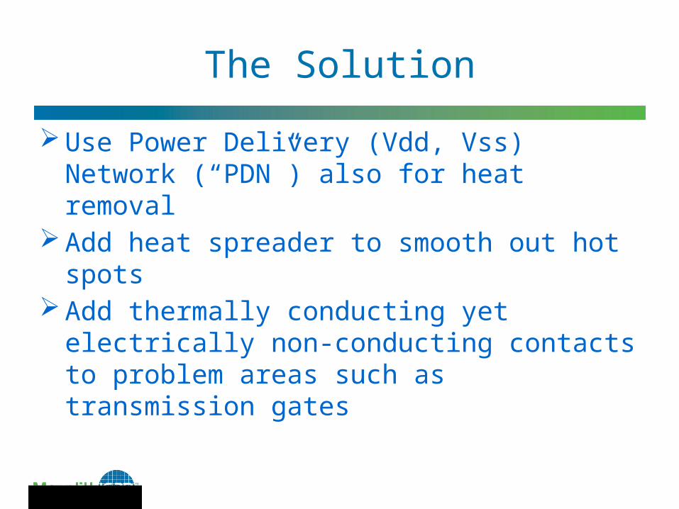
The Solution
Use Power Delivery (Vdd, Vss) Network (“PDN”) also for heat removal
Add heat spreader to smooth out hot spotsAdd thermally conducting yet electrically
non-conducting contacts to problem areas such as transmission gates
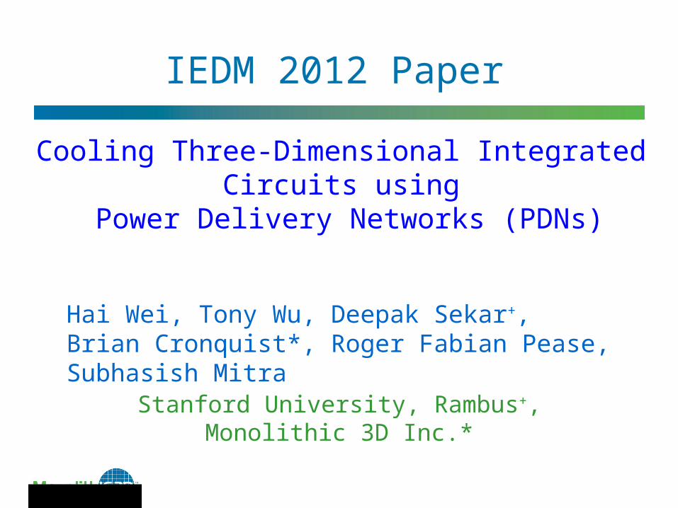
Cooling Three-Dimensional Integrated Circuits using
Power Delivery Networks (PDNs)
Hai Wei, Tony Wu, Deepak Sekar+, Brian Cronquist*, Roger Fabian Pease, Subhasish MitraStanford University, Rambus+, Monolithic 3D
Inc.*
55
IEDM 2012 Paper

Monolithic 3D Heat Removal Architecture (Achievable with Monolithic 3D
vertical interconnect density)
Global power grid shared among multiple device layers, local power grid for each device layer
Local VDD grid architecture shown above
Optimize all cells in library to have low thermal resistance to VDD/VSS lines (local heat sink)
px
py
Patented and Patent Pending Technology
20
60
100
140
0 10 20 30 40Tem
pe
ratu
re (
ºC)
× 100 TSVs /mm2
Monolithic 3D IC
Without Power Grid
With Power Grid
Signal wire
Heat sink

Power Delivery (Vdd, Vss) Network Provide effective Heat Removal Path
Related Documents