Actual Size: 2.28 x 1.45 x 0.5in 57,9 x 36,8 x 12,7mm Output Ripple Attenuation Module MicroRAM™ Rev 2.3 vicorpower.com Page 1 of 19 06/2017 800 927.9474 MicroRAM™ Features & Benefits • RoHS Compliant (with F or G pin option) • >40dB ripple attenuation from 1.1kHz to 1MHz • >40dB ripple attenuation from 100Hz to 1.1kHz with additional component • Integrated OR’ing diode supports N+1 redundancy • Significantly improves load transient response • Efficiency up to 98% • User selectable performance optimization • Combined active and passive filtering • 3 – 30V DC input range • 20 and 30 Ampere ratings Product Highlights Vicor’s MicroRAM output ripple attenuation module combines both active and passive filtering to achieve greater than 40dB of noise attenuation from 1.1kHz to 1Mhz. The lower frequency limit can be extended down to 100Hz, with greater than 40dB of attenuation, with the addition of a single external capacitor. The MicroRAM operates over a range of 3 to 30V DC , is available in either 20 or 30A models and is compatible with most manufacturers switching converters including all Vicor DC-DC converter models. The MicroRAM’s closed loop architecture greatly improves load transient response and can insure precise point of load voltage regulation using its SC function. The MicroRAM supports redundant and parallel operation with its integrated OR’ing diode function. It is available in Vicor’s standard Micro package (quarter brick) with a variety of terminations for through hole, socket or surface mount applications. Thermal Resistance Parameter Typ Unit Baseplate to sink flat, greased surface 0.16 °C/Watt with thermal pad (P/N 20265) 0.14 °C/Watt Baseplate to ambient free convection 8.0 °C/Watt 1000LFM 1.9 °C/Watt µRAM 2 C 2 1 Product Baseplate 1 = Slotted 2 = Threaded 3 = Thru-hole Pin Style 1 = Short Pin 2 = Long Pin S = Short ModuMate [1] N = Long ModuMate [1] F = Short RoHS G = Long RoHS K = Extra Long RoHS [2] Product Grade Temperatures (°C) Grade Operating Storage C = – 20 to +100 – 40 to +125 T = – 40 to +100 – 40 to +125 H = – 40 to +100 – 55 to +125 M = – 55 to +100 – 65 to +125 Type 2 = 20 A 3 = 30 A Part Numbering Parameter Rating Unit Notes +IN to – IN 30 V DC Continuous 40 V DC 100ms Load current 40 A DC 10 second pulse V REF V IN ± 1V V DC Continuous Ripple Input (Vp-p) 100 mV 100Hz 100kHz 500 mV 100kHz – 2MHz Mounting torque 4 – 6 In. lbs 6 each, 4-40 screw (0.45 – 0.68) (Nm) Pin soldering temperature 500 (260) °F (°C) < 5sec; wave solder 750 (390) °F (°C) < 7sec; wave solder Absolute Maximum Ratings [1] Compatible with the ModuMate interconnect system for socketing and surface mounting [2] Not intended for socket or Surfmate mounting

Welcome message from author
This document is posted to help you gain knowledge. Please leave a comment to let me know what you think about it! Share it to your friends and learn new things together.
Transcript
Actual Size:2.28 x 1.45 x 0.5in57,9 x 36,8 x 12,7mm
Output Ripple Attenuation Module
MicroRAM™ Rev 2.3 vicorpower.comPage 1 of 19 06/2017 800 927.9474
MicroRAM™
Features & Benefits
• RoHS Compliant (with F or G pin option)
• >40dB ripple attenuation from 1.1kHz to 1MHz
• >40dB ripple attenuation from 100Hz to 1.1kHz with additional component
• Integrated OR’ing diode supports N+1 redundancy
• Significantly improves load transient response
• Efficiency up to 98%
• User selectable performance optimization
• Combined active and passive filtering
• 3 – 30VDC input range
• 20 and 30 Ampere ratings
Product Highlights
Vicor’s MicroRAM output ripple attenuation module combines both active and passive filtering to achieve greater than 40dB of noise attenuation from 1.1kHz to 1Mhz. The lower frequency limit can be extended down to 100Hz, with greater than 40dB of attenuation, with the addition of a single external capacitor. The MicroRAM operates over a range of 3 to 30VDC, is available in either 20 or 30A models and is compatible with most manufacturers switching converters including all Vicor DC-DC converter models.
The MicroRAM’s closed loop architecture greatly improves load transient response and can insure precise point of load voltage regulation using its SC function.
The MicroRAM supports redundant and parallel operation with its integrated OR’ing diode function. It is available in Vicor’s standard Micro package (quarter brick) with a variety of terminations for through hole, socket or surface mount applications.
Thermal Resistance
Parameter Typ UnitBaseplate to sink flat, greased surface 0.16 °C/Watt with thermal pad (P/N 20265) 0.14 °C/WattBaseplate to ambient free convection 8.0 °C/Watt 1000LFM 1.9 °C/Watt
µRAM 2 C 2 1
Product Baseplate
1 = Slotted 2 = Threaded 3 = Thru-hole
Pin Style 1 = Short Pin 2 = Long Pin S = Short ModuMate [1]
N = Long ModuMate [1]
F = Short RoHS G = Long RoHSK = Extra Long RoHS [2]
Product Grade Temperatures (°C)Grade Operating Storage C = –20 to +100 –40 to +125 T = –40 to +100 –40 to +125 H = –40 to +100 –55 to +125 M = –55 to +100 –65 to +125
Type
2 = 20 A 3 = 30 A
Part Numbering
Parameter Rating Unit Notes
+IN to – IN 30 VDC Continuous
40 VDC 100ms
Load current 40 ADC 10 second pulse
VREF VIN ± 1V VDC Continuous
Ripple Input (Vp-p) 100 mV 100Hz 100kHz
500 mV 100kHz – 2MHz
Mounting torque 4 – 6 In. lbs 6 each, 4-40 screw (0.45 – 0.68) (Nm)
Pin soldering temperature 500 (260) °F (°C) <5sec; wave solder
750 (390) °F (°C) <7sec; wave solder
Absolute Maximum Ratings
[1] Compatible with the ModuMate interconnect system for socketing and surface mounting[2] Not intended for socket or Surfmate mounting
MicroRAM™ Rev 2.3 vicorpower.comPage 2 of 19 06/2017 800 927.9474
MicroRAM™
µRAM MODULE SPECIFICATIONS
(-20°C to +100°C baseplate temperature)
Electrical Characteristics
Electrical characteristics apply over the full operating range of input voltage, output power and baseplate temperature, unless otherwise specified.
All temperatures refer to the operating temperature at the center of the baseplate.
{1] The headroom voltage VHR is the voltage difference between the VIN+ and the VOUT+ pins of the µRAM.
[2] The SC resistor is used to trim the converter’s output voltage (Vnom) to compensate for the headroom voltage drop of the µRAM when remote sense is not used. This feature can only be used with converter’s that have a trim reference range between 1.21 and 1.25V.
Table 1 — Calculated values of RSC and RHR for a headroom voltage of 375mV. Use notes 1 and 2 to compute RSC and RHR values for different headroom voltages.
Parameter Min Typ Max Unit Notes
Operating current rangeµRAM2XXX
0.02 20 A No internal current limiting. Converter input must be properly fused such that the µRAM output current does not exceed the maximum operating current rating by more than 30% under a steady state condition.
Operating current rangeµRAM3XXX
0.02 30 A
Operating input voltage 3.0 30 V Continuous
Transient output responseLoad current step < 1A/µsec
50 mVp-p Step load change; see Figures 20, 23, & 26, pp. 16–17
Transient output responseLoad current step < 1A/µsec(CTRAN = 820µF)
50 mVp-pOptional capacitance CTRAN can be used to increase transient current capability; See Figures 21, 24 & 27, pp. 16–17
Recommended headroom voltagerange (VHR) @ 1A load [1] 325 425 mV
See Figures 4 and 5, pp. 5 for detailed explanation. See Table 1 for typical headroom setting resistor values.
Output ripple
Input Vp-p = 100mV
10 mVp-p Ripple frequency of 60Hz to 100kHz; optional CHR capacitor of 100µF required to increase low frequency attenuation as shown in Figure 2, pp. 35 MVRMS
Output ripple
Input Vp-p = 500mV
10 mVp-pRipple frequency of 100kHz to 2MHz; as shown in Figure 2, pp. 3
5 MVRMS
SC output voltage [2] 1.23 VDC See table 1 for typical RSC values, note 2 for calculation.
OR’ing threshold -10 mV VIN – VOUT
µRAM bias current 60 mA
Power dissipationµRAM2XXX VHR = 380mV @ 1A
7.5 W VIN = 28V; IOUT = 20A
Power dissipationµµRAM3XXX VHR = 380mV @ 1A
11.5 W VIN = 28V; IOUT = 30A
µRAM Output Voltage VHR @ 1A RHR Value (Ω) RSC Value (Ω)
3V 375mV 18.2k 442?
5V 375mV 30.9k 2.05k
12V 375mV 73.2k 7.68k
15V 375mV 90.9k 10.20k
24V 375mV 147.0k 17.40k
28V 375mV 174.0k 21.00k
VOUT+
VHR
RHR = • 2.3k (See Table 1 for example RHR values)
(VNOM • 1k)
1.23VRSC = – 2k (See Table 1 for example RSC values)
MicroRAM™ Rev 2.3 vicorpower.comPage 3 of 19 06/2017 800 927.9474
MicroRAM™
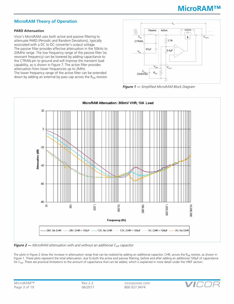
MicroRAM Theory of Operation
PARD Attenuation
Vicor’s MicroRAM uses both active and passive filtering to attenuate PARD (Periodic and Random Deviations), typically associated with a DC to DC converter’s output voltage. The passive filter provides effective attenuation in the 50kHz to 20MHz range. The low frequency range of the passive filter (ie; resonant frequency) can be lowered by adding capacitance to the CTRAN pin to ground and will improve the transient load capability, as is shown in Figure 7. The active filter provides attenuation from lower frequencies up to 2MHz. The lower frequency range of the active filter can be extended down by adding an external by-pass cap across the RHR resistor.
The plots in Figure 2 show the increase in attenuation range that can be realized by adding an additional capacitor, CHR, across the RHR resistor, as shown in Figure 1. These plots represent the total attenuation, due to both the active and passive filtering, before and after adding an additional 100µF of capacitance for CHR. There are practical limitations to the amount of capacitance that can be added, which is explained in more detail under the VREF section.
RHR
2.3kVIN+ VOUT+
VREF
9.4µF
VOUT-
57µF
CTRAN
VIN-
VHR
ActivePassive VDIODE
CHR(Optional)
Figure 1 — Simplified MicroRAM Block Diagram
Figure 2 — MicroRAM attenuation with and without an additional CHR capacitor
MicroRAM™ Rev 2.3 vicorpower.comPage 4 of 19 06/2017 800 927.9474
MicroRAM™
PARD Attenuation (Cont.)
Active attenuation is achieved by using power MOSFETs as a variable resistor that can dynamically change its impedance in order to maintain a constant output voltage, equal to the voltage programmed on its reference pin. When the input is lower, the active loop reduces the FET’s resistance, lowering the overall voltage drop across the MicroRAM. When the input is higher, the resistance is increased, increasing the voltage drop across the MicroRAM. The bandwidth of the active loop must be sufficiently higher than the converters control loop so it does not introduce significant phase shift to the sense loop of the converter.
There are both upper and lower limits to the range of resistance variations. The lower limit is based on the path resistance between VIN+ and VOUT+ and the amount of current passing through the MicroRAM. On the high end, the resistance of the FET, and therefore the maximum voltage drop, is limited to the voltage when the body diode of the FET starts to conduct and ripple passes through it to the output, exhibiting positive peaks of ripple at the load.
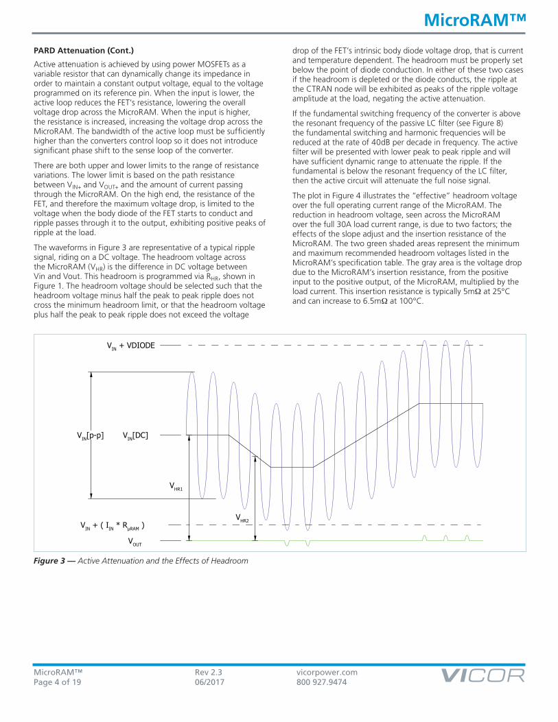
The waveforms in Figure 3 are representative of a typical ripple signal, riding on a DC voltage. The headroom voltage across the MicroRAM (VHR) is the difference in DC voltage between Vin and Vout. This headroom is programmed via RHR, shown in Figure 1. The headroom voltage should be selected such that the headroom voltage minus half the peak to peak ripple does not cross the minimum headroom limit, or that the headroom voltage plus half the peak to peak ripple does not exceed the voltage
drop of the FET’s intrinsic body diode voltage drop, that is current and temperature dependent. The headroom must be properly set below the point of diode conduction. In either of these two cases if the headroom is depleted or the diode conducts, the ripple at the CTRAN node will be exhibited as peaks of the ripple voltage amplitude at the load, negating the active attenuation.
If the fundamental switching frequency of the converter is above the resonant frequency of the passive LC filter (see Figure 8) the fundamental switching and harmonic frequencies will be reduced at the rate of 40dB per decade in frequency. The active filter will be presented with lower peak to peak ripple and will have sufficient dynamic range to attenuate the ripple. If the fundamental is below the resonant frequency of the LC filter, then the active circuit will attenuate the full noise signal.
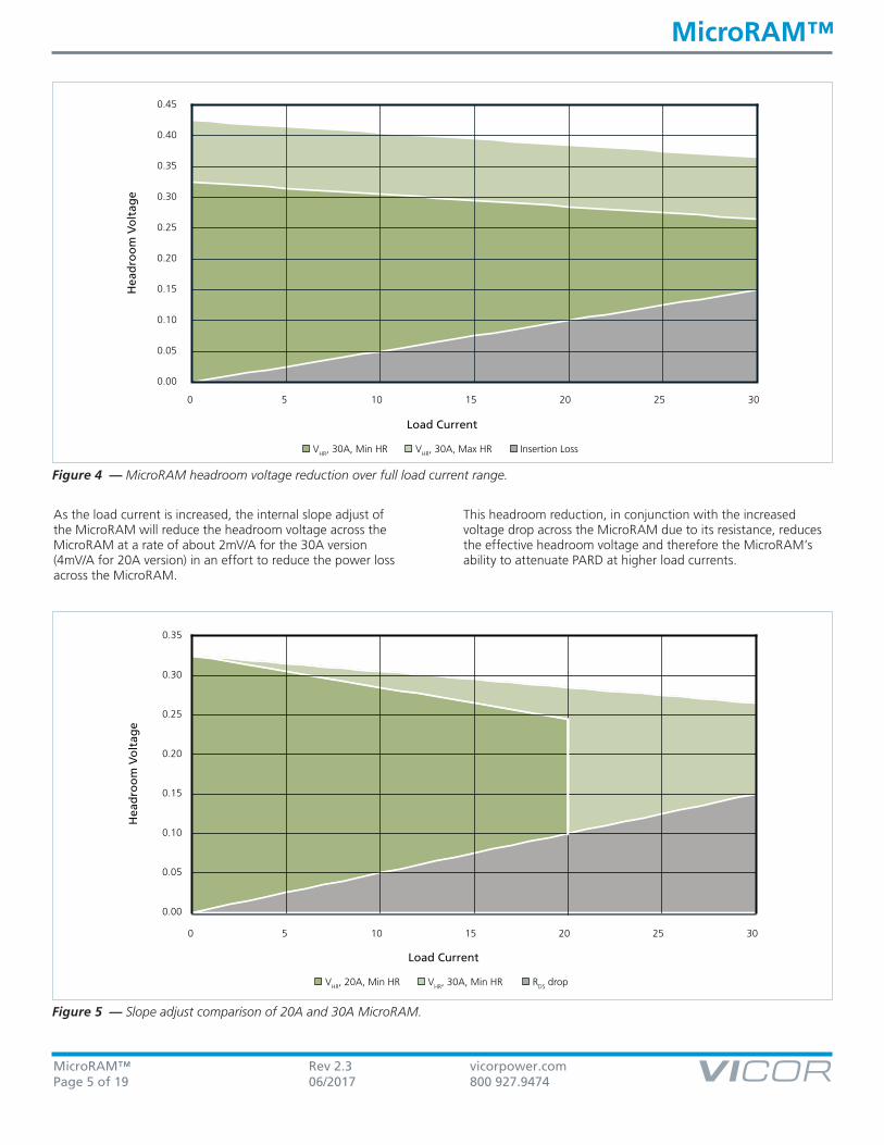
The plot in Figure 4 illustrates the “effective” headroom voltage over the full operating current range of the MicroRAM. The reduction in headroom voltage, seen across the MicroRAM over the full 30A load current range, is due to two factors; the effects of the slope adjust and the insertion resistance of the MicroRAM. The two green shaded areas represent the minimum and maximum recommended headroom voltages listed in the MicroRAM’s specification table. The gray area is the voltage drop due to the MicroRAM’s insertion resistance, from the positive input to the positive output, of the MicroRAM, multiplied by the load current. This insertion resistance is typically 5mΩ at 25°C and can increase to 6.5mΩ at 100°C.
VIN[p-p] VIN[DC]
VIN + VDIODE
VIN + ( IIN * RµRAM )
VOUT
VHR1
VHR2
Figure 3 — Active Attenuation and the Effects of Headroom
MicroRAM™ Rev 2.3 vicorpower.comPage 5 of 19 06/2017 800 927.9474
MicroRAM™
As the load current is increased, the internal slope adjust of the MicroRAM will reduce the headroom voltage across the MicroRAM at a rate of about 2mV/A for the 30A version (4mV/A for 20A version) in an effort to reduce the power loss across the MicroRAM.
This headroom reduction, in conjunction with the increased voltage drop across the MicroRAM due to its resistance, reduces the effective headroom voltage and therefore the MicroRAM’s ability to attenuate PARD at higher load currents.
0.00
0.05
0.10
0.15
0.20
0.25
0.30
0.35
0.40
0.45
0 5 10 15 20 25 30
Hea
dro
om
Vo
ltag
e
Load Current
VHR
, 30A, Min HR VHR
, 30A, Max HR Insertion Loss
Figure 4 — MicroRAM headroom voltage reduction over full load current range.
Hea
dro
om
Vo
ltag
e
Load Current
VHR
, 20A, Min HR VHR
, 30A, Min HR RDS
drop
0.00
0.05
0.10
0.15
0.20
0.25
0.30
0.35
0 5 10 15 20 25 30
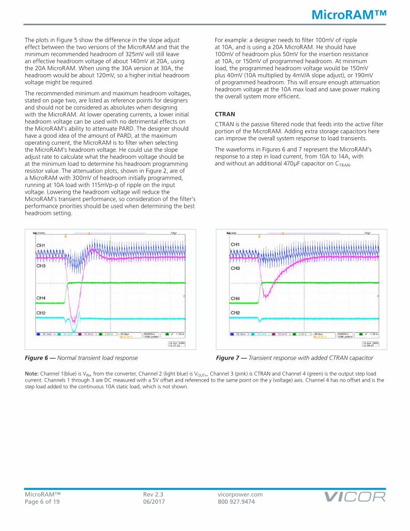
Figure 5 — Slope adjust comparison of 20A and 30A MicroRAM.
MicroRAM™ Rev 2.3 vicorpower.comPage 6 of 19 06/2017 800 927.9474
MicroRAM™
The plots in Figure 5 show the difference in the slope adjust effect between the two versions of the MicroRAM and that the minimum recommended headroom of 325mV will still leave an effective headroom voltage of about 140mV at 20A, using the 20A MicroRAM. When using the 30A version at 30A, the headroom would be about 120mV, so a higher initial headroom voltage might be required.
The recommended minimum and maximum headroom voltages, stated on page two, are listed as reference points for designers and should not be considered as absolutes when designing with the MicroRAM. At lower operating currents, a lower initial headroom voltage can be used with no detrimental effects on the MicroRAM’s ability to attenuate PARD. The designer should have a good idea of the amount of PARD, at the maximum operating current, the MicroRAM is to filter when selecting the MicroRAM’s headroom voltage. He could use the slope adjust rate to calculate what the headroom voltage should be at the minimum load to determine his headroom programming resistor value. The attenuation plots, shown in Figure 2, are of a MicroRAM with 300mV of headroom initially programmed, running at 10A load with 115mVp-p of ripple on the input voltage. Lowering the headroom voltage will reduce the MicroRAM’s transient performance, so consideration of the filter’s performance priorities should be used when determining the best headroom setting.
For example: a designer needs to filter 100mV of ripple at 10A, and is using a 20A MicroRAM. He should have 100mV of headroom plus 50mV for the insertion resistance at 10A, or 150mV of programmed headroom. At minimum load, the programmed headroom voltage would be 150mV plus 40mV (10A multiplied by 4mV/A slope adjust), or 190mV of programmed headroom. This will ensure enough attenuation headroom voltage at the 10A max load and save power making the overall system more efficient.
CTRAN
CTRAN is the passive filtered node that feeds into the active filter portion of the MicroRAM. Adding extra storage capacitors here can improve the overall system response to load transients.
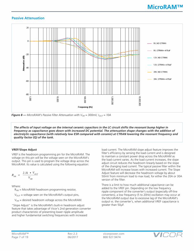
The waveforms in Figures 6 and 7 represent the MicroRAM’s response to a step in load current, from 10A to 14A, with and without an additional 470µF capacitor on CTRAN.
Figure 6 — Normal transient load response Figure 7 — Transient response with added CTRAN capacitor
Note: Channel 1(blue) is VIN+ from the converter, Channel 2 (light blue) is VOUT+, Channel 3 (pink) is CTRAN and Channel 4 (green) is the output step load current. Channels 1 through 3 are DC measured with a 5V offset and referenced to the same point on the y (voltage) axis. Channel 4 has no offset and is the step load added to the continuous 10A static load, which is not shown.
MicroRAM™ Rev 2.3 vicorpower.comPage 7 of 19 06/2017 800 927.9474
MicroRAM™
VREF/Slope Adjust
VREF is the headroom programming pin for the MicroRAM. The voltage on this pin will be the voltage seen on the MicroRAM’s output. This pin is used to program the voltage drop across the MicroRAM. Its value is calculated using the following equation:
Where: RHR = MicroRAM headroom programming resistor,
VOUT = voltage seen on the MicroRAM’s output pins,
VHR = desired headroom voltage across the MicroRAM.
“Slope Adjust” is the MicroRAM’s built-in headroom adjust feature that takes advantage of Vicor’s 2nd generation converter product characteristic of presenting lower ripple amplitude and higher fundamental switching frequencies with increased
load current. The MicroRAM slope adjust feature improves the filter’s efficiency by sensing the load current and is designed to maintain a constant power drop across the MicroRAM as the load current varies. As the load current increases, the slope adjust circuit reduces the headroom linearly based on the slope of the changing load current. The typical passive filter within the MicroRAM will increase losses with increased current. The Slope Adjust feature will decrease the headroom voltage by about 50mV from minimum load to max load, for either the 20A or 30A version of the filter.
There is a limit to how much additional capacitance can be added to the VREF pin. Depending on the low frequency ripple component of the converter’s output (especially off-line converters), a low frequency (5 to 20Hz) oscillation may occur at the MicroRAM output due to excessive lag of the MicroRAM’s output vs. the converter’s, when additional VREF capacitance is greater than 50µF.
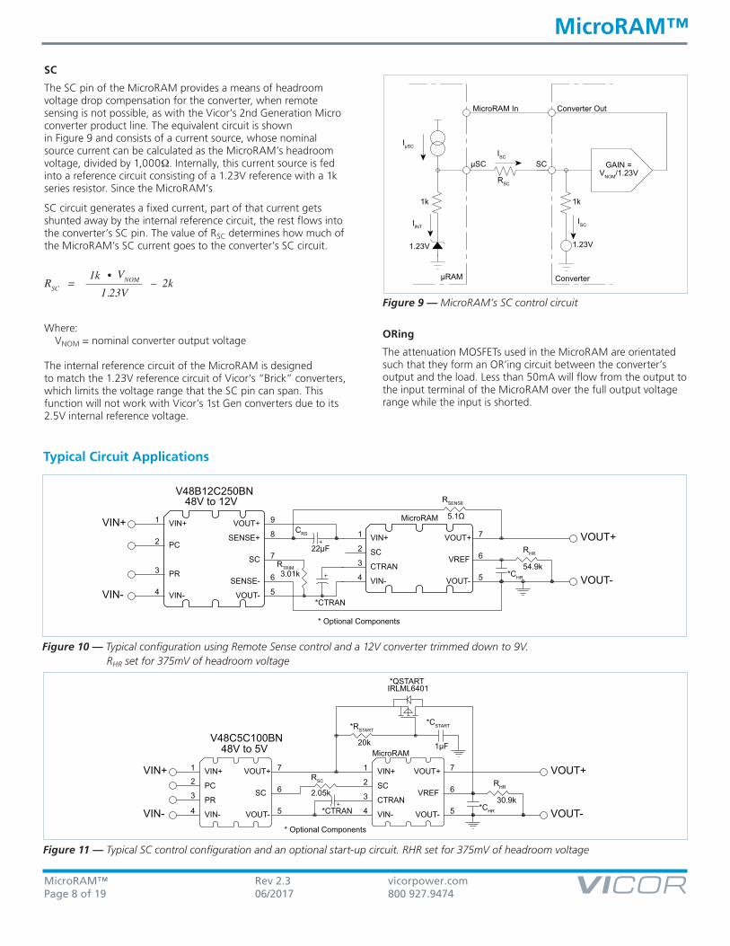
Figure 8 — MicroRAM’s Passive Filter Attenuation with VHR = 300mV, IOUT = 10A
Passive Attenuation
The affects of input voltage on the internal ceramic capacitors in the LC circuit shifts the resonant bump higher in frequency as capacitance goes down with increased DC potential. The attenuation shape changes with the addition of electrolytic capacitance (with relatively low ESR compared with ceramic) at CTRAN lowering the resonant frequency and quality factor (Q) of the tank.
2.3k • VOUT
VHR
RHR =
MicroRAM™ Rev 2.3 vicorpower.comPage 8 of 19 06/2017 800 927.9474
MicroRAM™
SC
The SC pin of the MicroRAM provides a means of headroom voltage drop compensation for the converter, when remote sensing is not possible, as with the Vicor’s 2nd Generation Micro converter product line. The equivalent circuit is shown in Figure 9 and consists of a current source, whose nominal source current can be calculated as the MicroRAM’s headroom voltage, divided by 1,000Ω. Internally, this current source is fed into a reference circuit consisting of a 1.23V reference with a 1k series resistor. Since the MicroRAM’s
SC circuit generates a fixed current, part of that current gets shunted away by the internal reference circuit, the rest flows into the converter’s SC pin. The value of RSC determines how much of the MicroRAM’s SC current goes to the converter’s SC circuit.
Where: VNOM = nominal converter output voltage The internal reference circuit of the MicroRAM is designed to match the 1.23V reference circuit of Vicor’s “Brick” converters, which limits the voltage range that the SC pin can span. This function will not work with Vicor’s 1st Gen converters due to its 2.5V internal reference voltage.
ORing
The attenuation MOSFETs used in the MicroRAM are orientated such that they form an OR’ing circuit between the converter’s output and the load. Less than 50mA will flow from the output to the input terminal of the MicroRAM over the full output voltage range while the input is shorted.
Typical Circuit Applications
VIN+1
CTRAN3SC2
VIN-4
VOUT+ 7
VREF 6
VOUT- 5
MicroRAM
VIN+1
PRSC 6
VIN-4
VOUT+ 7
PC
VOUT- 5
V48C5C100BN48V to 5V
30.9k
RHR2.05k
RSC2
3
VIN+
VIN- *CTRAN *CHR
*QSTARTIRLML6401
1µF
*CSTART
20k
*RSTART
VOUT+
VOUT-* Optional Components
Figure 11 — Typical SC control configuration and an optional start-up circuit. RHR set for 375mV of headroom voltage
VIN+1
PR3SC 7
VIN-4
VOUT+ 9
PC2
VOUT- 5SENSE- 6
SENSE+ 8
V48B12C250BN48V to 12V
VIN+
VIN-
22µF
CRS
5.1Ω
RSENSE
*CTRAN
54.9k
RHR
*CHR
VOUT+
VOUT-
VIN+1
CTRAN3SC2
VIN-4
VOUT+ 7
VREF 6
VOUT- 5
MicroRAM
3.01kRTRIM
* Optional Components
Figure 10 — Typical configuration using Remote Sense control and a 12V converter trimmed down to 9V. RHR set for 375mV of headroom voltage
IµSC
1k
1.23V
1k
1.23V
ConverterRAMµ
RSC
GAIN =VNOM/1.23V
ISC
Converter Out
SCSCµ
IINT
MicroRAM In
ISC
Figure 9 — MicroRAM’s SC control circuit
1k • VNOM
1.23VRSC = – 2k
MicroRAM™ Rev 2.3 vicorpower.comPage 9 of 19 06/2017 800 927.9474
MicroRAM™
In Figure 10, a 48V to 12V Vicor Mini converter is used to create a 9V output supply. The converter is trimmed down from 12V to 9V, using a 3.01k resistor from the converter’s SC to its VOUT- pins, then uses the remote sense pins, along with the RRS and CRS components, to maintain proper output voltage and converter stability. Again, the headroom voltage is designed to be 375mV.
The circuit shown in Figure 11 is of a Vicor Micro 48V to 5VDC to DC converter with a MicroRAM, set to have 375mV of headroom voltage drop across it. To compensate for the headroom drop, the MicroRAM’s SC circuit is used to adjust the converter to have 5.375V on its output, so the voltage seen on the MicroRAM’s output is 5V.
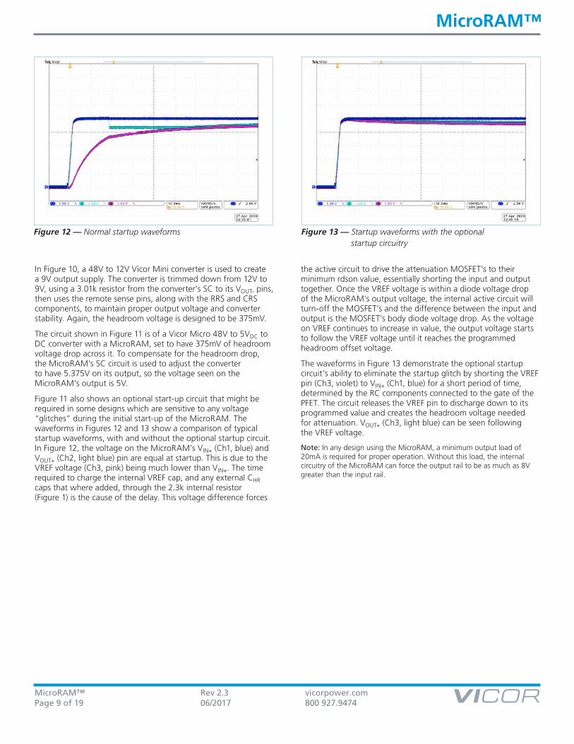
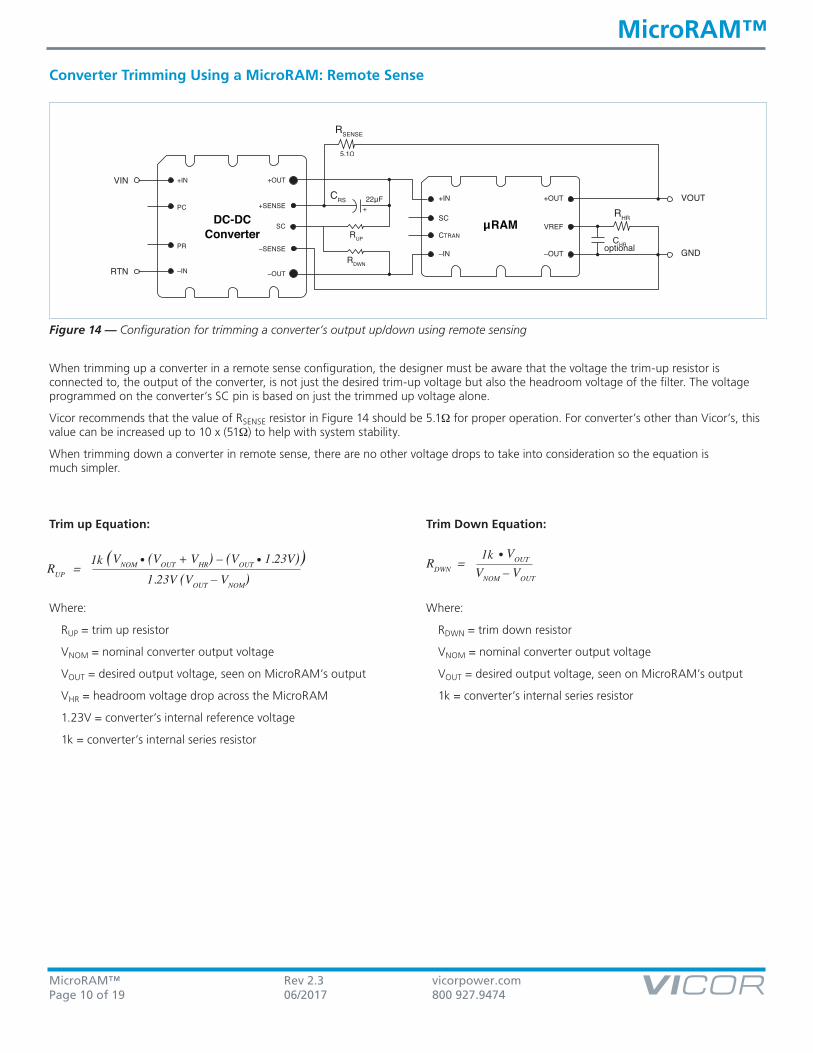
Figure 11 also shows an optional start-up circuit that might be required in some designs which are sensitive to any voltage “glitches” during the initial start-up of the MicroRAM. The waveforms in Figures 12 and 13 show a comparison of typical startup waveforms, with and without the optional startup circuit. In Figure 12, the voltage on the MicroRAM’s VIN+ (Ch1, blue) and VOUT+ (Ch2, light blue) pin are equal at startup. This is due to the VREF voltage (Ch3, pink) being much lower than VIN+. The time required to charge the internal VREF cap, and any external CHR caps that where added, through the 2.3k internal resistor (Figure 1) is the cause of the delay. This voltage difference forces
the active circuit to drive the attenuation MOSFET’s to their minimum rdson value, essentially shorting the input and output together. Once the VREF voltage is within a diode voltage drop of the MicroRAM’s output voltage, the internal active circuit will turn-off the MOSFET’s and the difference between the input and output is the MOSFET’s body diode voltage drop. As the voltage on VREF continues to increase in value, the output voltage starts to follow the VREF voltage until it reaches the programmed headroom offset voltage.
The waveforms in Figure 13 demonstrate the optional startup circuit’s ability to eliminate the startup glitch by shorting the VREF pin (Ch3, violet) to VIN+ (Ch1, blue) for a short period of time, determined by the RC components connected to the gate of the PFET. The circuit releases the VREF pin to discharge down to its programmed value and creates the headroom voltage needed for attenuation. VOUT+ (Ch3, light blue) can be seen following the VREF voltage.
Note: In any design using the MicroRAM, a minimum output load of 20mA is required for proper operation. Without this load, the internal circuitry of the MicroRAM can force the output rail to be as much as 8V greater than the input rail.
Figure 12 — Normal startup waveforms Figure 13 — Startup waveforms with the optional startup circuitry
MicroRAM™ Rev 2.3 vicorpower.comPage 10 of 19 06/2017 800 927.9474
MicroRAM™
Converter Trimming Using a MicroRAM: Remote Sense
+OUT
VREF
–OUT
+IN
SC
CTRAN
–IN
RSENSE
CRS 22µF
5.1Ω
+ RHRDC-DCConverter
+OUT
+SENSE
SC
–SENSE
–OUT
+IN
PC
PR
–IN
µRAM
VOUT
GND
VIN
RTN
RUP
RDWN
CHRoptional
Figure 14 — Configuration for trimming a converter’s output up/down using remote sensing
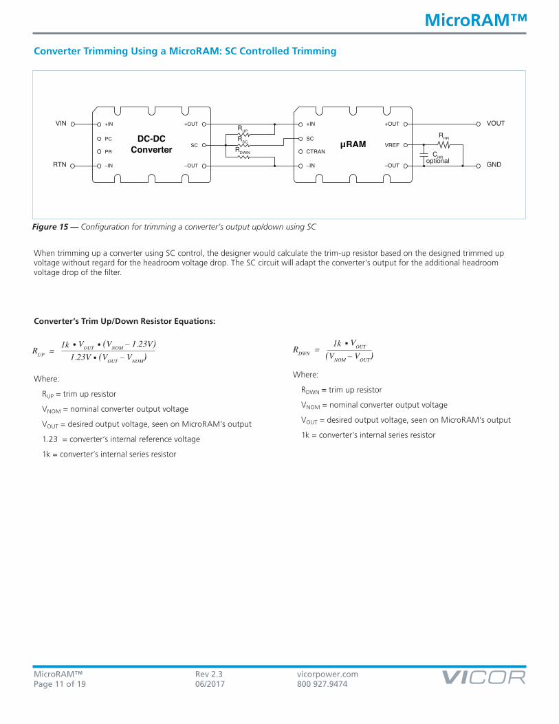
When trimming up a converter in a remote sense configuration, the designer must be aware that the voltage the trim-up resistor is connected to, the output of the converter, is not just the desired trim-up voltage but also the headroom voltage of the filter. The voltage programmed on the converter’s SC pin is based on just the trimmed up voltage alone.
Vicor recommends that the value of RSENSE resistor in Figure 14 should be 5.1Ω for proper operation. For converter’s other than Vicor’s, this value can be increased up to 10 x (51Ω) to help with system stability.
When trimming down a converter in remote sense, there are no other voltage drops to take into consideration so the equation is much simpler.
Trim up Equation:
Where:
RUP = trim up resistor
VNOM = nominal converter output voltage
VOUT = desired output voltage, seen on MicroRAM’s output
VHR = headroom voltage drop across the MicroRAM
1.23V = converter’s internal reference voltage
1k = converter’s internal series resistor
Trim Down Equation:
Where:
RDWN = trim down resistor
VNOM = nominal converter output voltage
VOUT = desired output voltage, seen on MicroRAM’s output
1k = converter’s internal series resistor
1k (VNOM • (VOUT + VHR) – (VOUT • 1.23V))1.23V (VOUT – VNOM)
RUP =1k • VOUT
VNOM – VOUT
RDWN =
MicroRAM™ Rev 2.3 vicorpower.comPage 11 of 19 06/2017 800 927.9474
MicroRAM™
Converter Trimming Using a MicroRAM: SC Controlled Trimming
DC-DCConverter
+OUT
SC
–OUT
+IN
PC
PR
–IN
µRAM
+OUT
VREF
–OUT
+IN
SC
CTRAN
–IN
RSC
RDWIN
RUP
VIN
RTN
VOUT
GND
RHR
CHRoptional
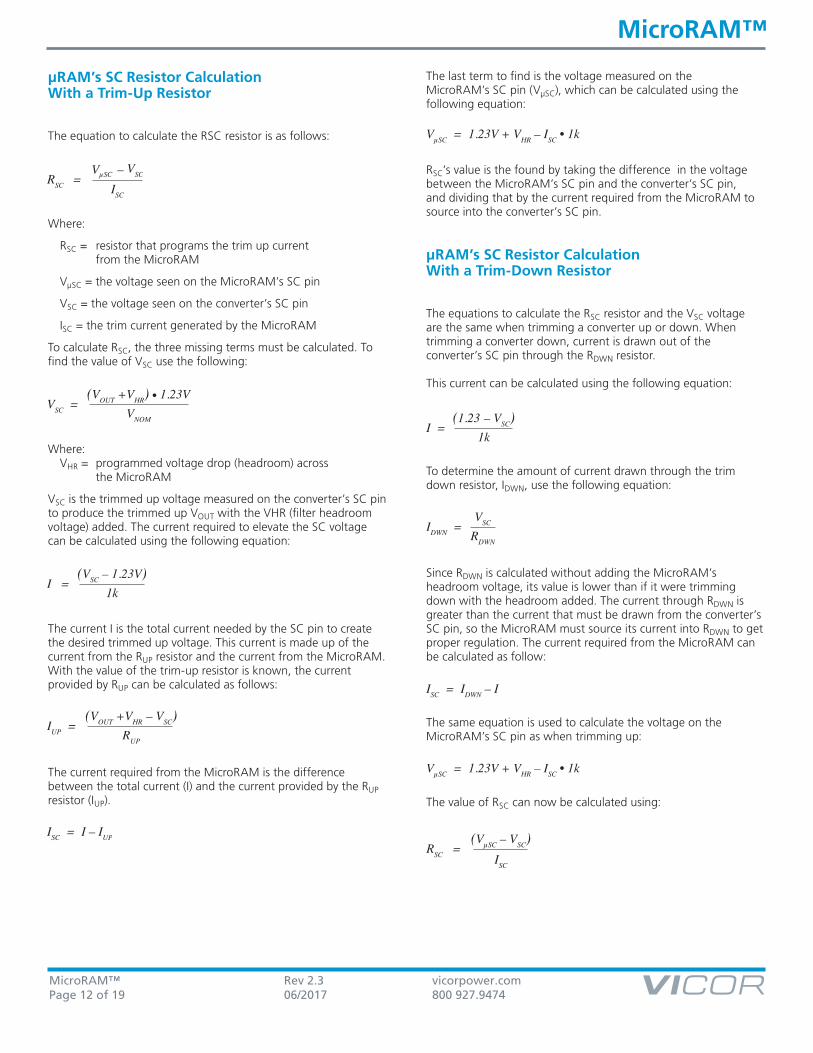
Figure 15 — Configuration for trimming a converter’s output up/down using SC
Converter’s Trim Up/Down Resistor Equations:
Where:
RUP = trim up resistor
VNOM = nominal converter output voltage
VOUT = desired output voltage, seen on MicroRAM’s output
1.23 = converter’s internal reference voltage
1k = converter’s internal series resistor
Where:
RDWN = trim up resistor
VNOM = nominal converter output voltage
VOUT = desired output voltage, seen on MicroRAM’s output
1k = converter’s internal series resistor
When trimming up a converter using SC control, the designer would calculate the trim-up resistor based on the designed trimmed up voltage without regard for the headroom voltage drop. The SC circuit will adapt the converter’s output for the additional headroom voltage drop of the filter.
1k • VOUT • (VNOM – 1.23V)1.23V • (VOUT – VNOM)RUP =
1k • VOUT
(VNOM – VOUT)RDWN =
MicroRAM™ Rev 2.3 vicorpower.comPage 12 of 19 06/2017 800 927.9474
MicroRAM™
µRAM’s SC Resistor Calculation With a Trim-Up Resistor
The equation to calculate the RSC resistor is as follows:
Where:
RSC = resistor that programs the trim up current from the MicroRAM
VµSC = the voltage seen on the MicroRAM’s SC pin
VSC = the voltage seen on the converter’s SC pin
ISC = the trim current generated by the MicroRAM
To calculate RSC, the three missing terms must be calculated. To find the value of VSC use the following:
Where: VHR = programmed voltage drop (headroom) across the MicroRAM
VSC is the trimmed up voltage measured on the converter’s SC pin to produce the trimmed up VOUT with the VHR (filter headroom voltage) added. The current required to elevate the SC voltage can be calculated using the following equation:
The current I is the total current needed by the SC pin to create the desired trimmed up voltage. This current is made up of the current from the RUP resistor and the current from the MicroRAM. With the value of the trim-up resistor is known, the current provided by RUP can be calculated as follows:
The current required from the MicroRAM is the difference between the total current (I) and the current provided by the RUP resistor (IUP).
The last term to find is the voltage measured on the MicroRAM’s SC pin (VµSC), which can be calculated using the following equation:
RSC’s value is the found by taking the difference in the voltage between the MicroRAM’s SC pin and the converter’s SC pin, and dividing that by the current required from the MicroRAM to source into the converter’s SC pin.
µRAM’s SC Resistor Calculation With a Trim-Down Resistor
The equations to calculate the RSC resistor and the VSC voltage are the same when trimming a converter up or down. When trimming a converter down, current is drawn out of the converter’s SC pin through the RDWN resistor. This current can be calculated using the following equation:
To determine the amount of current drawn through the trim down resistor, IDWN, use the following equation:
Since RDWN is calculated without adding the MicroRAM’s headroom voltage, its value is lower than if it were trimming down with the headroom added. The current through RDWN is greater than the current that must be drawn from the converter’s SC pin, so the MicroRAM must source its current into RDWN to get proper regulation. The current required from the MicroRAM can be calculated as follow:
The same equation is used to calculate the voltage on the MicroRAM’s SC pin as when trimming up:
The value of RSC can now be calculated using:
VµSC – VSC
ISC
RSC =
(VOUT +VHR) • 1.23VVNOM
VSC =
(VSC – 1.23V)1k
I =
(VOUT +VHR – VSC)RUP
IUP =
ISC = I – IUP
VµSC = 1.23V + VHR – ISC • 1k
(1.23 – VSC)1k
I =
VSC
RDWN
IDWN =
ISC = IDWN – I
VµSC = 1.23V + VHR – ISC • 1k
(VµSC – VSC)ISC
RSC =
MicroRAM™ Rev 2.3 vicorpower.comPage 13 of 19 06/2017 800 927.9474
MicroRAM™
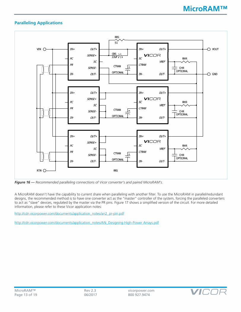
Paralleling Applications
Figure 16 — Recommended paralleling connections of Vicor converter’s and paired MicroRAM’s.
A MicroRAM doesn’t have the capability to current share when paralleling with another filter. To use the MicroRAM in parallel/redundant designs, the recommended method is to have one converter act as the “master” controller of the system, forcing the paralleled converters to act as “slave” devices, regulated by the master via the PR pins. Figure 17 shows a simplified version of the circuit. For more detailed information, please refer to these Vicor application notes:
http://cdn.vicorpower.com/documents/application_notes/an2_pr-pin.pdf
http://cdn.vicorpower.com/documents/application_notes/AN_Designing High-Power Arrays.pdf

MicroRAM™ Rev 2.3 vicorpower.comPage 14 of 19 06/2017 800 927.9474
MicroRAM™
PICOR’s Filter Calculator Application
To make the task of calculating the required external resistors much easier, Picor has developed a filter calculator program that is designed to be used with Vicor’s MicroRAM output filter, as well as with Picor’s QPO output filters. The filter program will automatically calculate any trim resistors that might be required, in either remote sense or SC control modes, and all the external resistors required by the filter. The resulting values are of standard 1% tolerance resistors.
Figure 17 — Screen shots of Picor’s Filter Calculator program for determining the external resistor values used in the circuits of Figures 10 and 11
Note: The screen shots shown in Figure 17 are of Picor’s output filter calculator program, a tool which can be used to calculate the resistor values needed in the circuits shown in Figure 10 and Figure 11. This program is a Windows based executable file that is available to Vicor Applications Engineering, and which can also made available to our customers upon request. To request a copy of the program please contact your local Vicor Field Applications Engineer or email your request to [email protected].

MicroRAM™ Rev 2.3 vicorpower.comPage 15 of 19 06/2017 800 927.9474
MicroRAM™
APPLICATION NOTES
Load capacitance can affect the overall phase margin of the MicroRAM active loop as well as the phase margin of the converter loop. The distributed variables such as inductance of the load path, the capacitor type and value as well as its ESR and ESL also affect transient capability at the load. The following guidelines are based on circuit simulation and should be considered when point of load capacitance is used with the MicroRAM in order to maintain a minimum of 30° of phase margin.
Using ceramic load capacitance with <1milliohm ESR and <1nH ESL:
20µF to 200µF requires 20nH of trace/wire load path inductance
200µF to 1,000µF requires 60nH of trace/wire load path inductance
For the case where load capacitance is connected directly to the output of the MicroRAM, i.e. no trace inductance, and the ESR is >1 milliohm:
20µF to 200µF load capacitance needs an ESL of >50nH
200µF to 1,000µF load capacitance needs an ESL of >5nH
Adding low ESR capacitance directly at the output terminals of MicroRAM is not recommended and may cause stability problems.
In practice the distributed board or wire inductance at a load or on a load board will be sufficient to isolate the output of the MicroRAM from any load capacitance and minimize any appreciable effect on phase margin.
Recommended PCB Layout
To achieve the best attenuation, proper routing of the power nodes must be followed. The VIN- and VOUT- are internally connected within the MicroRAM module and should not be connected externally. Doing so will create a ground loop and will degrade attenuation results. All measurements should be made using the VOUT- of the MicroRAM as reference ground. If possible, waveform measurements should be made with an oscilloscope that is AC line isolated from other test equipment, and should use probes without the grounding clip attached. Please contact [email protected] for of proper PARD measurements techniques.
Figure 18 — Recommended copper patterns, top view
MicroRAM™ Rev 2.3 vicorpower.comPage 16 of 19 06/2017 800 927.9474
MicroRAM™
Figure 24 — V300B12C250B and µRAM; Input and output dynamic response CTRAN = 820µF Electrolytic; 30% of load step of 6A (10A – 16A); RHR = 80k (Configured as in Figure 8 w/o Trim)
Figure 23 — V300B12C250B and µRAM; Input and output dynamic response no added CTRAN; 17.5% of 20A rating load step of 3.5A (10A – 13.5A); RHR = 80 k (Configured as in Figure 7 w/o Trim)
Figure 22 — V375B12C250B and µRAM; Input and output ripple @50% (10A) load CH1 = Vi; CH2 = Vo; Vi-Vo = 305mV; RHR = 80k (Configured as in Figure 7 w/o Trim)
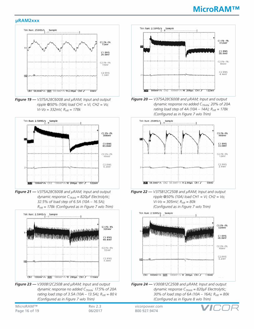
Figure 20 — V375A28C600B and µRAM; Input and output dynamic response no added CTRAN; 20% of 20A rating load step of 4A (10A – 14A); RHR = 178k (Configured as in Figure 7 w/o Trim)
Figure 21 — V375A28C600B and µRAM; Input and output dynamic response CTRAN = 820µF Electrolytic; 32.5% of load step of 6.5A (10A – 16.5A); RHR = 178k (Configured as in Figure 7 w/o Trim)
Figure 19 — V375A28C600B and µRAM; Input and output ripple @50% (10A) load CH1 = Vi; CH2 = Vo; Vi-Vo = 332mV; RHR = 178k
µRAM2xxx
MicroRAM™ Rev 2.3 vicorpower.comPage 17 of 19 06/2017 800 927.9474
MicroRAM™
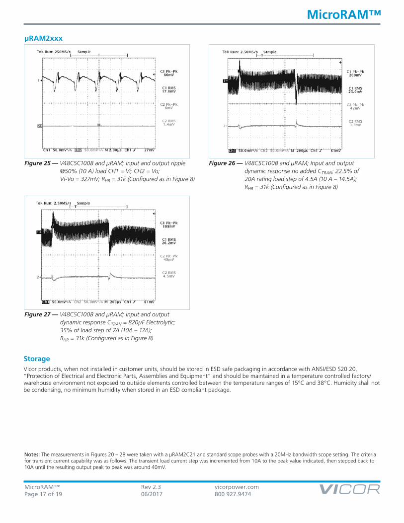
µRAM2xxx
Figure 26 — V48C5C100B and µRAM; Input and output dynamic response no added CTRAN; 22.5% of 20A rating load step of 4.5A (10 A – 14.5A); RHR = 31k (Configured as in Figure 8)
Figure 27 — V48C5C100B and µRAM; Input and output dynamic response CTRAN = 820µF Electrolytic; 35% of load step of 7A (10A – 17A); RHR = 31k (Configured as in Figure 8)
Figure 25 — V48C5C100B and µRAM; Input and output ripple @50% (10 A) load CH1 = Vi; CH2 = Vo; Vi-Vo = 327mV; RHR = 31k (Configured as in Figure 8)
Notes: The measurements in Figures 20 – 28 were taken with a µRAM2C21 and standard scope probes with a 20MHz bandwidth scope setting. The criteria for transient current capability was as follows: The transient load current step was incremented from 10A to the peak value indicated, then stepped back to 10A until the resulting output peak to peak was around 40mV.
StorageVicor products, when not installed in customer units, should be stored in ESD safe packaging in accordance with ANSI/ESD S20.20, “Protection of Electrical and Electronic Parts, Assemblies and Equipment” and should be maintained in a temperature controlled factory/ warehouse environment not exposed to outside elements controlled between the temperature ranges of 15°C and 38°C. Humidity shall not be condensing, no minimum humidity when stored in an ESD compliant package.
MicroRAM™ Rev 2.3 vicorpower.comPage 18 of 19 06/2017 800 927.9474
MicroRAM™
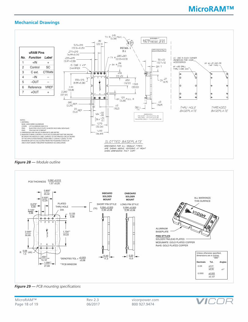
Mechanical Drawings
NOTES:1. MATERIAL: BASE: 6000 SERIES ALUMINUM COVER: LCP, ALUMINUM 3003 H14 PINS: RoHS PINS GOLD PLATE 30 MICRO INCH MIN; NON-RoHS PINS: TIN/LEAD 90/10 BRIGHT2. DIMENSIONS AND VALUES IN BRACKETS ARE METRIC3. MANUFACTURING CONTROL IS IN PLACE TO ENSURE THAT THE SPACING BETWEEN THE MODULES LABEL SURFACE TO THE PRINTED CIRCUIT BOARD OF THE APPLICATION RANGES FROM DIRECT CONTACT (ZERO), TO THE MAXIMUM GAP AS CALCULATED FROM THE TOLERANCE STACK-UP AND IS NOT SUBJECT NEGATIVE TOLERANCE ACCUMULATION
DIMENSION LPIN SHORT – .55±.015 [14.0±.38]PIN LONG–– .63±.015 [16.0±.38]
PIN EXTRA LONG–––- .71±.015 [18.0±.38]
uRAM Pins No. Function Label 1 +IN + 2 Control SC 3 C ext. CTRAN 4 –IN – 5 –OUT – 6 Reference VREF 7 +OUT +
Figure 28 — Module outline
PINS STYLES SOLDER:TIN/LEAD PLATEDMODUMATE: GOLD PLATED COPPERRoHS: GOLD PLATED COPPER
ALUMINUMBASEPLATE
2 3
6
1
7
4
5
PLATEDTHRU HOLE
DIA
±0,08*DENOTES TOL =
0.1333,38
1.734**44,04
.400*10,16
1.090**27,69
0.145*3,68
0.800*20,32
0.525*13,34
0.275*6,99
2.000*50,80
0.061,5R (4X)
INBOARDSOLDERMOUNT
SHORT PIN STYLE0.094 ±0.003 2,39 ±0,08
0.4511,5
ALL MARKINGSTHIS SURFACE
(7X)
**PCB WINDOW
PCB THICKNESS 0.062 ±0.0101,57 ±0,25
SURFACE MOUNTSOCKET
N/A0.183 ±0.003 4,65 ±0,08
0.5614,2
0.4611,7
SOCKETS0.080" DIA PINS (7X)P/N 13632 (100 pcs.)P/N 16023 (7 pc. kit)
SOCKET HEADERS(SURFACE MOUNT)
KIT INCLUDES INPUT & OUTPUT
P/N 16025
INBOARDSOCKETMOUNT
ONBOARDSOCKET
SURFACE MOUNT
0.5313,5
ONBOARDSOLDERMOUNT
LONG PIN STYLE0.094 ±0.003 2,39 ±0,08
±0.003
Unless otherwise specified, dimensions are in inches mm
Decimals Tol. Angles
0.XX ±0.01 ±0,25 ±1°
0.XXX ±0.005 ±0,127
Figure 29 — PCB mounting specifications

MicroRAM™ Rev 2.3 vicorpower.comPage 19 of 19 06/2017 800 927.9474
MicroRAM™
Vicor’s comprehensive line of power solutions includes high density AC-DC and DC-DC modules and accessory components, fully configurable AC-DC and DC-DC power supplies, and complete custom power systems.
Information furnished by Vicor is believed to be accurate and reliable. However, no responsibility is assumed by Vicor for its use. Vicor makes no representations or warranties with respect to the accuracy or completeness of the contents of this publication. Vicor reserves the right to make changes to any products, specifications, and product descriptions at any time without notice. Information published by Vicor has been checked and is believed to be accurate at the time it was printed; however, Vicor assumes no responsibility for inaccuracies. Testing and other quality controls are used to the extent Vicor deems necessary to support Vicor’s product warranty. Except where mandated by government requirements, testing of all parameters of each product is not necessarily performed.
Specifications are subject to change without notice.
Visit http://www.vicorpower.com/dc-dc/filters/output-ripple-attenuator-modu-1 for the latest product information.
Vicor’s Standard Terms and Conditions and Product Warranty
All sales are subject to Vicor’s Standard Terms and Conditions of Sale, and Product Warranty which are available on Vicor’s webpage (http://www.vicorpower.com/termsconditionswarranty) or upon request.
Life Support Policy
VICOR’S PRODUCTS ARE NOT AUTHORIZED FOR USE AS CRITICAL COMPONENTS IN LIFE SUPPORT DEVICES OR SYSTEMS WITHOUT THE EXPRESS PRIOR WRITTEN APPROVAL OF THE CHIEF EXECUTIVE OFFICER AND GENERAL COUNSEL OF VICOR CORPORATION. As used herein, life support devices or systems are devices which (a) are intended for surgical implant into the body, or (b) support or sustain life and whose failure to perform when properly used in accordance with instructions for use provided in the labeling can be reasonably expected to result in a significant injury to the user. A critical component is any component in a life support device or system whose failure to perform can be reasonably expected to cause the failure of the life support device or system or to affect its safety or effectiveness. Per Vicor Terms and Conditions of Sale, the user of Vicor products and components in life support applications assumes all risks of such use and indemnifies Vicor against all liability and damages.
Intellectual Property Notice
Vicor and its subsidiaries own Intellectual Property (including issued U.S. and Foreign Patents and pending patent applications) relating to the products described in this data sheet. No license, whether express, implied, or arising by estoppel or otherwise, to any intellectual property rights is granted by this document. Interested parties should contact Vicor’s Intellectual Property Department.
Vicor Corporation25 Frontage Road
Andover, MA, USA 01810Tel: 800-735-6200Fax: 978-475-6715
emailCustomer Service: [email protected]
Technical Support: [email protected]
Related Documents