Micromechanical tunable Fabry-P´ erot interferometers with membrane Bragg mirrors based on silicon/silicon carbonitride Zur Erlangung des akademischen Grades eines DOKTORS DER NATURWISSENSCHAFTEN von der KIT-Fakult¨ at f¨ ur Physik des Karlsruher Instituts f¨ ur Technologie (KIT) genehmigte DISSERTATION von MSc Christian Huber aus T¨ ubingen Tag der m¨ undlichen Pr¨ ufung : 18. Januar 2019 Referent : Prof. Dr. Heinz Kalt Korreferent : Prof. Dr. David Hunger

Welcome message from author
This document is posted to help you gain knowledge. Please leave a comment to let me know what you think about it! Share it to your friends and learn new things together.
Transcript
Micromechanical tunableFabry-Perot interferometers
with membrane Bragg mirrorsbased on silicon/silicon carbonitride
Zur Erlangung des akademischen Grades einesDOKTORS DER NATURWISSENSCHAFTEN
von der KIT-Fakultat fur Physikdes Karlsruher Instituts fur Technologie (KIT)
genehmigte
DISSERTATION
von
MSc Christian Huberaus Tubingen
Tag der mundlichen Prufung : 18. Januar 2019Referent : Prof. Dr. Heinz KaltKorreferent : Prof. Dr. David Hunger

Prufungskomission:
Prof. Dr. H. KaltProf. Dr. D. HungerProf. Dr. W. WulfhekelPriv.-Doz. Dr. B. NarozhnyProf. Dr. D. Zeppenfeld
Karlsruhe Institute of Technology (KIT)Institute of Applied PhysicsWolfgang-Gaede-Straße 176131 KarlsruheGermanyAG Kalt: http://www.aph.kit.edu/kaltChristian Huber: [email protected]
Robert Bosch GmbHRobert-Bosch-Campus 171272 RenningenGermanyChristian Huber: [email protected]
This work was supported by the Karlsruhe School of Optics and Photonics (KSOP).
Contents
1 Introduction 1
2 Overview of miniaturized spectrometers 52.1 Categorization of miniaturized spectrometers by detector type . . . . 6
2.1.1 Generalized description of a spectrometer . . . . . . . . . . . . 62.1.2 Static spectrometers with array detectors . . . . . . . . . . . . 92.1.3 Tunable spectrometers with single detectors . . . . . . . . . . 13
2.2 Principles of near infrared spectroscopy and its applications . . . . . 162.3 Conclusion: Fabry-Perot interferometers for low-cost miniaturized
near infrared spectrometers . . . . . . . . . . . . . . . . . . . . . . . 19
3 Fundamentals of Fabry-Perot interferometers 213.1 The ideal Fabry-Perot interferometer (FPI) . . . . . . . . . . . . . . . 22
3.1.1 The transmittance spectrum of an ideal FPI . . . . . . . . . . 223.1.2 Tunable FPIs as filters for spectrometers . . . . . . . . . . . . 24
3.2 Peak broadening in a real FPI . . . . . . . . . . . . . . . . . . . . . . 263.2.1 Types of defects and their contribution to the effective finesse 273.2.2 Optimization of integral transmittance in the presence of defects 29
3.3 FPIs based on distributed Bragg reflectors . . . . . . . . . . . . . . . 323.3.1 Working principles of distributed Bragg reflectors . . . . . . . 323.3.2 Influence of the Bragg reflector’s phase shift upon
reflection on FPI transmittance . . . . . . . . . . . . . . . . . 363.3.3 FPIs with asymmetric mirrors . . . . . . . . . . . . . . . . . . 38
3.4 Summary: Low-order FPIs for tunable filters with broad spectralworking range . . . . . . . . . . . . . . . . . . . . . . . . . . . . . . . 39
4 Broadband near infrared MEMS Fabry-Perot interferometers:Opportunities and challenges 414.1 State of the art of MEMS FPIs . . . . . . . . . . . . . . . . . . . . . 42
4.1.1 Surface vs. bulk micromachining approaches . . . . . . . . . . 424.1.2 Comparison of mirror concepts . . . . . . . . . . . . . . . . . 46
I
4.1.3 Overview of published designs . . . . . . . . . . . . . . . . . . 474.2 Limitations of surface-micromachined FPIs . . . . . . . . . . . . . . . 51
4.2.1 Influence of the low-refractive index materialin the Bragg reflector . . . . . . . . . . . . . . . . . . . . . . . 52
4.2.2 Pull-in limitation of the travel range . . . . . . . . . . . . . . 554.2.3 Stress-induced substrate curvature . . . . . . . . . . . . . . . 57
4.3 Proposition: Double membrane FPIs for increased spectral workingranges and large diameters . . . . . . . . . . . . . . . . . . . . . . . . 60
5 Amorphous hydrogenated silicon carbonitridefor MEMS applications 635.1 Deposition and possible applications of SiCN . . . . . . . . . . . . . . 645.2 Influence of deposition temperature on material properties . . . . . . 65
5.2.1 Elemental composition and density . . . . . . . . . . . . . . . 665.2.2 Bonding structure . . . . . . . . . . . . . . . . . . . . . . . . . 685.2.3 Complex refractive index . . . . . . . . . . . . . . . . . . . . . 715.2.4 Mechanical stress . . . . . . . . . . . . . . . . . . . . . . . . . 755.2.5 Aging under ambient air . . . . . . . . . . . . . . . . . . . . . 77
5.3 Stress tuning by thermal annealing . . . . . . . . . . . . . . . . . . . 805.4 Vapor HF resistance . . . . . . . . . . . . . . . . . . . . . . . . . . . 825.5 Other properties relevant to MEMS fabrication . . . . . . . . . . . . 835.6 Summary: Process conditions for low refractive index, tensile
and HF resistant PECVD SiCN . . . . . . . . . . . . . . . . . . . . . 84
6 Design and fabrication of near infrared Fabry-Perot interferometerswith silicon/silicon carbonitride based Bragg mirrors 876.1 Optical design of single and double membrane FPIs . . . . . . . . . . 886.2 Actuation and pull-in behavior of the designed FPIs . . . . . . . . . . 946.3 Filter fabrication process . . . . . . . . . . . . . . . . . . . . . . . . . 976.4 Selected characterization steps during fabrication . . . . . . . . . . . 101
6.4.1 Reflectance and stress of single mirrors . . . . . . . . . . . . . 1026.4.2 Mirror blistering during annealing . . . . . . . . . . . . . . . . 1036.4.3 Mirror layer delamination during prolonged HF etching . . . . 1046.4.4 Stiction-free release of first order FPIs at large
membrane diameters . . . . . . . . . . . . . . . . . . . . . . . 1066.5 Summary: SiCN-based double membrane FPI proof-of-principle devices108
7 Static Fabry-Perot interferometers with membrane mirrors 1117.1 Stress determination from the vibrational excitation spectrum
of released membranes . . . . . . . . . . . . . . . . . . . . . . . . . . 1127.2 Surface flatness of the upper membrane mirror . . . . . . . . . . . . . 115
II
7.2.1 Comparison of profilometric and white lightinterferometric surface profile measurements . . . . . . . . . . 115
7.2.2 Membrane flatness in the presence of anisotropic in-plane stress1177.3 Local probing of FPIs by spatially-resolved transmittance measurements119
7.3.1 Derivation of the optical gap width from spatially-resolvedtransmittance spectra . . . . . . . . . . . . . . . . . . . . . . . 119
7.3.2 Single point vs. full aperture FPI transmittancemeasurements . . . . . . . . . . . . . . . . . . . . . . . . . . . 122
7.4 Optical gap homogeneity of single and double membrane FPIs . . . . 1237.4.1 Stress-induced inhomogeneity in the optical gap of
single membrane FPIs . . . . . . . . . . . . . . . . . . . . . . 1247.4.2 Double membrane FPIs with highly homogeneous
optical gaps . . . . . . . . . . . . . . . . . . . . . . . . . . . . 1257.4.3 Decoupling of resolution and throughput in
double membrane FPIs . . . . . . . . . . . . . . . . . . . . . . 1287.5 Summary: Double membrane FPIs for large-area, high-resolution filters130
8 Actuated Fabry-Perot interferometers 1338.1 Actuated single membrane FPIs limited by electrostatic pull-in . . . . 134
8.1.1 The surface profile of the moving membrane mirror . . . . . . 1348.1.2 Transmittance peak tuning within the first FSR . . . . . . . . 136
8.2 Actuated double membrane FPIs without pull-in limitation . . . . . . 1408.2.1 The influence of actuation voltages on the upper
membrane mirror profile . . . . . . . . . . . . . . . . . . . . . 1418.2.2 Transmittance peak tuning over the full first FSR . . . . . . . 142
8.3 Summary: Double membrane FPIs for broad spectral working ranges 146
9 Conclusion and outlook 147
A List of equipment and processes 151
B Optical setup for spatially-resolved transmittance measurements 157
C Refractive index data for optical simulations 161
D Pull-in for actuation of membranes with generalized ring electrodes163
List of publications 167
Abbreviations and symbols 169
References 177
Acknowledgments 199
III

IV
Chapter 1
Introduction
Sensors based on microelectromechanical systems (MEMS) play an indispensablerole in many of today’s applications from consumer electronics to the automotiveindustry [1,2]. Originating from the silicon-based microelectronics industry, MEMStechnology allows fabrication of movable structures which can be used both as actu-ators and transducers in order to cause and detect displacement of seismic masses,respectively. Thereby, measurement of manifold mechanical quantities such as linearand angular acceleration or pressure has been enabled and has now reached a levelof maturity where these sensors can be fabricated at low cost, small size and highprecision [1].
Microoptoelectromechanical systems (MOEMS) expand the field of these applica-tions by introducing additional optical functionality. Typical examples for MOEMSinclude reflective devices such as digital light projectors (DLPs) or scanning mirrorsas well as devices for telecom applications such as optical switches [3]. Close inte-gration of optical and MEMS elements opens new fields of sensors beyond humansensing [2], which is why new MOEMS devices continue to be developed to this day.
Spectroscopic devices (spectrometers, hyperspectral imagers) are an example forsuch a novel kind of sensor technology which can enable new applications outsidethe scope of traditional MEMS sensors. In fact, much of our current knowledgeabout both the atomic and vibrational structure of matter stems from spectroscopyof emitted, transmitted or reflected light in the visible and infrared part of theelectromagnetic spectrum, respectively. At present, spectroscopic methods are notonly used in research but are also well established in, e.g., the chemical industry forprocess and quality control. Typically, the employed laboratory spectrometers offerhigh spectral resolution but are bulky and expensive.
1
Chapter 1. Introduction
Development of miniaturized versions of such spectroscopic devices began towardsthe end of the last century [4, 5]. However, during the last decade research effortshave increased significantly with the aim to open new spectroscopic applicationsoutside laboratories, where both size and cost rather than high-end precision mat-ter [6]. The development is also driven by the fact that nowadays algorithms forextracting relevant information from measured spectra as well as the required com-putational capacity in portable devices are readily available. Popularity of the topicis reflected by an increasing amount of popular scientific journal contributions or on-line PR articles reporting miniaturized spectrometers with the potential of becominga ”tricorder” known from the famous Star Trek series, which can identify arbitrarymaterials [7–9]. It has to be noted that, apart from a few exceptions [10, 11], theseresearch devices are not mature enough to reach market entry level so that a truecommercialization of spectroscopy for everyone has not taken place yet.
Several reported approaches combine known types of spectrometers such as gratingspectrometers [12] or Fourier transform spectrometers [13] with MEMS technology inorder to shrink their size and benefit from cost advantages at large scale production.Additionally, MEMS-based Fabry-Perot interferometers (FPIs) have been demon-strated to be used as tunable filters in front of a single channel detector [14, 15].Such devices are formed by two highly reflective mirrors separated by an optical gapwhere at least one of the mirrors is movable in order to change the optical gap andthereby the filter transmittance wavelength.
Apart from the potential of small size and low cost, the FPI approach is very ver-satile, since the concept as such allows to address different wavelength ranges bya proper choice of non-absorptive mirror materials and adjusting respective devicedimensions. In the near infrared (NIR) spectral range ( to ) for ex-ample, a filter resolution below has already been demonstrated [11,16]. Thisis sufficient to resolve overtones of fundamental vibrational modes which govern therespective material reflectance spectra [15] and thereby makes material classificationfeasible.
For various reasons, however, the maximum spectral working range (SWR) in theNIR, which commercially available FPIs-based tunable filters can currently cover,is restricted to roughly – [11] (corresponding to of their designwavelength), which limits the range of possible applications. Furthermore, whenscaling up the optically active area in order to increase the optical throughput, thereis a risk of losing spectral resolution due to deviations from parallelism between themirrors [17,18].
This thesis aims at improving surface-micromachined MEMS FPIs in the NIR withrespect to both of the aforementioned shortcomings. This is achieved by introduc-
2
ing a new material for optical MEMS, silicon carbonitride (SiCN), which can bedeposited with a low refractive index while being resistant to vapor hydrofluoricacid (HF) etching. The resulting refractive index contrast to silicon enables fabri-cation of stable mirror membranes with a broad spectral range of high reflectance.Furthermore, a new MEMS FPI design called double membrane FPI is developedwhich comprises two released membrane mirrors instead of a single one as it is thecase in state of the art devices. With such a device architecture, the FPI transmit-tance wavelength can safely be tuned over a large spectral range. Furthermore, highspectral resolution can be maintained, independent of the membrane diameter. Inthis thesis, these proposed devices are designed, fabricated and characterized withrespect to the claimed improvements.
Structure of the thesis
Following this introduction, in chapter 2 the general field of miniaturized spec-trometers is introduced. The discussion of various existing spectrometer conceptsshows that for the NIR range FPI-based spectrometers possess significant advantagesregarding their cost and mass producibility.
In order to understand the working mechanism of such FPI-based spectrometers,chapter 3 reviews the required fundamentals of FPIs. Special attention is paid toFPIs with dielectric mirrors operated in low interference order as they are found inMEMS-based FPI spectrometers.
This sets the basis for discussing actual implementations of FPIs as MEMS devicesin chapter 4. The chapter starts with an overview of existing concepts. Subse-quently, root causes for the limitations of both the SWR and the filter resolutionat large membrane diameters are derived. As a result, the double membrane FPIstructure is proposed and the search for a low-refractive index, HF-resistant MEMSmaterial is motivated. It is the actual aim of this thesis to demonstrate the resultingimprovement in SWR.
A possible candidate for such a material is SiCN deposited by plasma-enhancedchemical vapor deposition (PECVD), which is introduced in chapter 5. SiCN isuncommon for MEMS applications [19] and its physical properties strongly dependon the deposition parameters [20]. Therefore, the effect of deposition temperatureon the relevant properties for this application, namely refractive index, mechanicalstress and vapor HF resistance, is investigated in detail. Results from this chapterhave been published in [21,22].
After having found a suitable low-refractive index material and determined its optical
3
Chapter 1. Introduction
properties, chapter 6 presents the actual design of the MEMS FPI devices used forthis thesis and makes predictions regarding their performance. Furthermore, theprocess flow for filter fabrication is shown and intermediate characterization resultsafter critical process steps are presented and discussed.
Chapter 7 shows characterization results regarding membrane flatness and mirrorparallelism both for the proposed double membrane as well as the existing singlemembrane FPI structure for unactuated, i.e., static filters. It is shown that in con-trast to single membrane FPIs, mirror parallelism does not depend on the membranediameter in double membrane FPIs which allows filter resolution to be decoupledfrom optical throughput. Results from this chapter have been published in [18].
The case of actuated FPIs is considered in chapter 8. It is demonstrated thatthe double membrane FPI structure indeed enables increasing the SWR to an un-precedented range of by circumventing its pull-in limitation found in singlemembrane FPIs. Results from this chapter have been published in [23].
Last, chapter 9 provides a summary of the presented results and gives an outlook onresearch questions and device optimizations which can be addressed in future work.
The appendix gives further details on the equipment used for fabrication and char-acterization. In particular, the custom-built spatially-resolved transmittance setupis described in detail. Furthermore, model parameters for the refractive indicesused in transfer-matrix simulations are given. Finally, a theory behind electrostaticactuation with a generalized ring electrode is developed.
4
Chapter 2
Overview of miniaturizedspectrometers
Traditionally, spectrometers are heavy and expensive laboratory equipment operatedby expert users who are trained to evaluate measured spectra. However, there aremany spectroscopic applications, e.g., in mineral exploration, safety screening ordrug testing, to name just a few, which can greatly benefit from doing a measurementin the field rather than bringing an analyte to a laboratory [6]. This has lead to thedevelopment of portable or even handheld spectrometers which are smaller, rugged,battery-powered and may include a light source. Furthermore, they can possess dataprocessing capabilities which help practitioners without spectroscopic knowledgeto perform a measurement and extract useful information about, e.g., qualitativematerial composition or quantitative content [24]. To that end, manufacturers canprovide and maintain high quality reference data libraries. Depending on the targetapplication, spectrometers working in the NIR, mid infrared (MIR) as well as Ramanspectrometers are available [24].
Such industrial and civilian scenarios require high accuracy and reliability on the onehand but on the other hand allow manufacturers to sell their spectrometers at a highunit price (>1000 $). During the last years, an alternative trend has evolved mainlyfrom the startup-scene which directly tries to target the consumer market by offeringlow-cost spectrometers [10] often working in the NIR. Such devices can make use ofcloud computing for spectra evaluation combined with crowd-sourced reference datalibraries [25, 26]. Proposed (and advertised) applications include food quality andadulteration monitoring [26], anti-counterfeiting or personal health tracking [6]. Inthis case, requirements regarding accuracy and reliability are less strict. However,low unit price (<100 $), small size and ease-of-use are mandatory.
5
Chapter 2. Overview of miniaturized spectrometers
This chapter serves as an introduction to the general field of miniaturized spectro-meters both from a technological and an application point of view. It starts with acomparison of different working principles for miniaturized spectrometers based ontheir detector type in section 2.1. This will provide a useful classification schemeand motivates the later choice of an FPI-based spectrometer as the technologicalapproach for this thesis.
Subsequently in section 2.2, possible applications in the NIR spectral region arepresented and some of the performance requirements which will serve as a guidelinelater are derived.
2.1 Categorization of miniaturized spectrometers
by detector type
For laboratories, there are two common types of spectrometers1. On the one hand,grating based spectrometers are used for the ultraviolet (UV) and visible (VIS)spectral range where shot noise is the dominant source of noise. On the other hand,Fourier-transform infrared (FTIR) spectrometers based on a Michelson interferome-ter provide a throughput and multiplex advantage in the infrared (IR) where theavailable detectors are limited by thermal noise.
Apart from miniaturized versions of these two types of spectrometers, a number ofother device architectures with the potential to be fabricated at small size have beenproposed [27–31]. In order to structure the following discussion of these approaches,the working principle of a spectrometer will first be treated from a generalized pointof view in subsection 2.1.1. Subsequently, selected miniaturized spectrometer con-cepts using an array detector and a single detector will be discussed in subsec-tion 2.1.2 and 2.1.3, respectively.
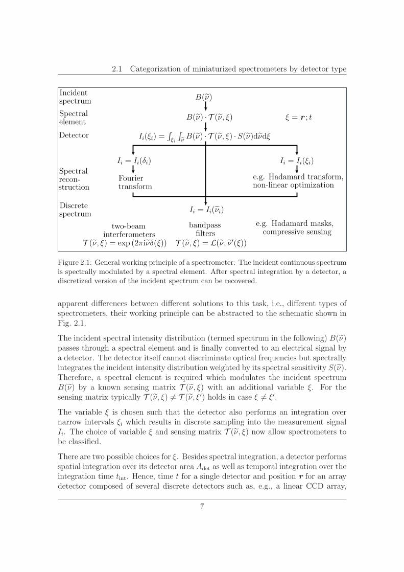
2.1.1 Generalized description of a spectrometer
The task of a spectrometer consists of sampling the continuous spectral intensitydistribution B(ν) of incident light into a series of discrete values Ii(νi) where νdenotes wavenumber. Ideally, such a spectrometer can operate over a broad SWRwith high spectral resolution and a large signal-to-noise-ratio (SNR). Despite the
1Raman spectroscopy is not within the scope of this thesis. Therefore, the following discussionwill not deal with high resolution spectrometers for the visible.
6
2.1 Categorization of miniaturized spectrometers by detector type
T (ν, ξ) = L(ν, ν ′(ξ))
Ii = Ii(δi) Ii = Ii(ξi)
B(ν)
B(ν) · T (ν, ξ)
Ii(ξi) =∫ξi
∫νB(ν) · T (ν, ξ) ·S(ν) ν ξ
Ii = Ii(νi)
T (ν, ξ) = (2πiνδ(ξ))
ξ = r ; t
Fouriertransform
e.g. Hadamard transform,non-linear optimization
Detector
Spectralrecon-struction
bandpassfilters
two-beaminterferometers
e.g. Hadamard masks,compressive sensing
Incidentspectrum
Spectralelement
Discretespectrum
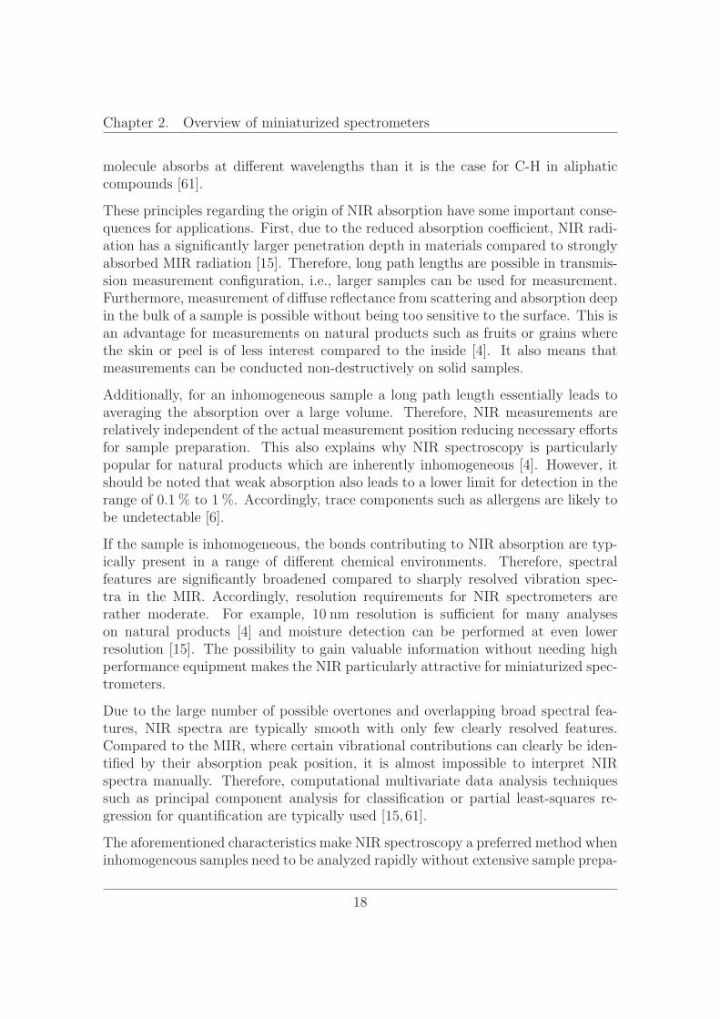
Figure 2.1: General working principle of a spectrometer: The incident continuous spectrumis spectrally modulated by a spectral element. After spectral integration by a detector, adiscretized version of the incident spectrum can be recovered.
apparent differences between different solutions to this task, i.e., different types ofspectrometers, their working principle can be abstracted to the schematic shown inFig. 2.1.
The incident spectral intensity distribution (termed spectrum in the following) B(ν)passes through a spectral element and is finally converted to an electrical signal bya detector. The detector itself cannot discriminate optical frequencies but spectrallyintegrates the incident intensity distribution weighted by its spectral sensitivity S(ν).Therefore, a spectral element is required which modulates the incident spectrumB(ν) by a known sensing matrix T (ν, ξ) with an additional variable ξ. For thesensing matrix typically T (ν, ξ) �= T (ν, ξ′) holds in case ξ �= ξ′.
The variable ξ is chosen such that the detector also performs an integration overnarrow intervals ξi which results in discrete sampling into the measurement signalIi. The choice of variable ξ and sensing matrix T (ν, ξ) now allow spectrometers tobe classified.
There are two possible choices for ξ. Besides spectral integration, a detector performsspatial integration over its detector area A as well as temporal integration over theintegration time t . Hence, time t for a single detector and position r for an arraydetector composed of several discrete detectors such as, e.g., a linear CCD array,
7
Chapter 2. Overview of miniaturized spectrometers
can serve as ξ (see examples below). The sensing matrix T (ν, ξ) can be constructedin various ways.
Band pass filters as spectral elements
A simple choice for the spectral element is a bandpass filter with the center passwavelength depending unambiguously on ξ, i.e., T (ν, ξ) = L(ν, ν ′(ξ)) where L(ν, ν ′)is the filter characteristic with its passband centered at ν ′. The resulting discretemeasurement values Ii can directly be mapped to the corresponding frequenciesgiven that ν ′(ξ) is known so that Ii = Ii(νi).
In this configuration, spectrometer resolution is given by the width of the passbandof L. The SWR depends on the number of channels ξi. As the major part of theincident light is blocked by the bandpass filter, spectrometers of that type only makeuse of a small portion of the incident energy per resolved spectral band. This is adisadvantage regarding the obtainable SNR at a given integration time compared tothe other spectrometer types discussed in the following.
The grating in a grating spectrometer is an example for such a spectral elementwhich acts as a bandpass filter. Within one diffraction order, it unambiguously mapsoptical frequency to diffraction angle which is subsequently mapped to position byan imaging optical element such as a focusing mirror. An array detector placed inthe focal plane then samples the spectrum at different points in space.
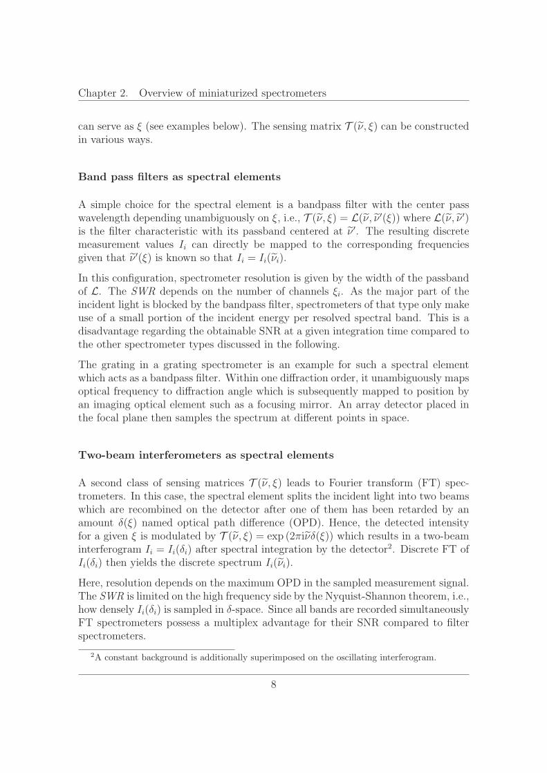
Two-beam interferometers as spectral elements
A second class of sensing matrices T (ν, ξ) leads to Fourier transform (FT) spec-trometers. In this case, the spectral element splits the incident light into two beamswhich are recombined on the detector after one of them has been retarded by anamount δ(ξ) named optical path difference (OPD). Hence, the detected intensityfor a given ξ is modulated by T (ν, ξ) = (2πiνδ(ξ)) which results in a two-beaminterferogram Ii = Ii(δi) after spectral integration by the detector2. Discrete FT ofIi(δi) then yields the discrete spectrum Ii(νi).
Here, resolution depends on the maximum OPD in the sampled measurement signal.The SWR is limited on the high frequency side by the Nyquist-Shannon theorem, i.e.,how densely Ii(δi) is sampled in δ-space. Since all bands are recorded simultaneouslyFT spectrometers possess a multiplex advantage for their SNR compared to filterspectrometers.
2A constant background is additionally superimposed on the oscillating interferogram.
8
2.1 Categorization of miniaturized spectrometers by detector type
In case of the Michelson interferometer mentioned before, the movable mirror per-forms a mapping of OPD to mirror position which is subsequently mapped to thetemporal domain. Hence, measurement takes place with a single detector at discretetime intervals.
Other spectral elements
Apart from these two common choices which correspond to well-known spectrom-eter types, other possibilities exist for the sensing matrix T (ν, ξ) which, similar toFT spectroscopy, require some form of spectral reconstruction to yield the discretespectrum Ii(νi). For example, T (ν, ξ) can take the form of a Hadamard matrixso that Ii(νi) is recovered by an inverse Hadamard transform [32]. Since severalwavenumber channels contribute to each ξi, there is a similar multiplex advantagefor the SNR as in FT spectrometers.
Recently, compressive sensing theory has also been used to reconstruct a discretespectrum Ii(νi) with a higher number of spectral bands than acquired in the measure-ment Ii(ξi) [33, 34]. In compressive sensing, given a known sensing matrix T (ν, ξ),non-linear optimization is used to reconstruct the discrete incident spectrum Ii(νi)which gives the best approximation to the measured signal Ii(ξi) [35]. As there areinfinite solutions to this problem due to the reduced dimensionality of Ii(ξi) com-pared to Ii(νi), optimization includes a regularization term constraining the normof Ii(νi). In other words, the incident spectrum Ii(νi) is expected to be the functionwith minimal complexity which would lead to the measured signal Ii(ξi) [35].
Based on this categorization, there is a total of six classes which the miniaturizedimplementations presented in the following can be attributed to. As discussed before,the choice of ξ leads to either array detectors for ξ = r or single pixel detectors forξ = t. Due to the resulting implications on the available spectral range for low-costspectrometers, these two cases will be discussed separately in the following.
2.1.2 Static spectrometers with array detectors
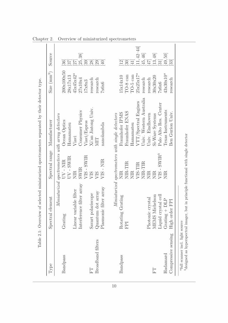
Miniaturized spectrometers with array detectors have been realized using a varietyof spectral elements with the devices ranging from pure research samples to readilyavailable products. Table 2.1 (top part) gives an overview of some selected devicesincluding their spectral element, coarse spectral range and original manufacturer orresearch institute, respectively. For reasons clarified below, the NIR range below
9
Chapter 2. Overview of miniaturized spectrometersTab
le2.1:Overview
ofselected
miniaturizedspectrometersseparatedbytheirdetectortype.
Type
Spectral
elem
ent
Spectral
range
Man
ufacturer
Size(
)Sou
rce
Miniaturizedspectrom
eterswitharraydetectors
Ban
dpass
Grating
UV
-NIR
Ocean
Optics
200x
100x
50[36]
UV
-SW
IRHam
amatsu
28x17x13
[37]
Linearvariab
lefilter
NIR
Viavi
45x45x42
a[27]
Interference
filter
array
SW
IRCon
sumer
Physics
27x10x4
[25,38]
VIS
-SW
IRViavi/Espros
17x8x
3[39]
FT
Savartpolariscope
VIS
Xi’an
JiatongUniv.
research
[28]
Broad
ban
dfilters
Quan
tum
dot
array
VIS
MIT
research
[29]
Plasm
onic
filter
array
VIS
-NIR
nan
olam
bda
7x6x
6[40]
Miniaturizedspectrom
eterswithsingledetectors
Ban
dpass
RotatingGrating
NIR
Fraunhofer
IPMS
15x14x10
[12]
FPI
NIR
-TIR
Fraunhofer
ENAS
TO-8
can
[30]
NIR
Ham
amatsu
TO-5
can
[41]
VIS-T
IRVTT/S
pectral
Engines
25x25x17
a[11,42–44]
NIR
-TIR
Univ.Western
Australia
research
[45,46]
Photon
iccrystal
NIR
Univ.Eindhoven
research
[47]
FT
MEMSMichelson
NIR
Si-WareSystem
s30x30x20
[13,48]
Liquid
crystal
cell
VIS
-SW
IRb
PaloAltoRes.Center
7x6x
6[31]
Had
amard
Grating+
DLP
NIR
Texas
Instruments
43x30x10
a[49,50]
Com
pressivesensing
Highorder
FPI
Ben
Gurion
Univ.
research
[33]
afullscanner
incl.lightsource
bdesigned
ashyperspectralim
ager,butin
principle
functionalwithsingle
detector
10

2.1 Categorization of miniaturized spectrometers by detector type
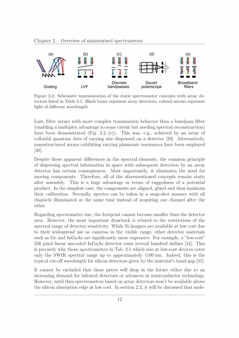
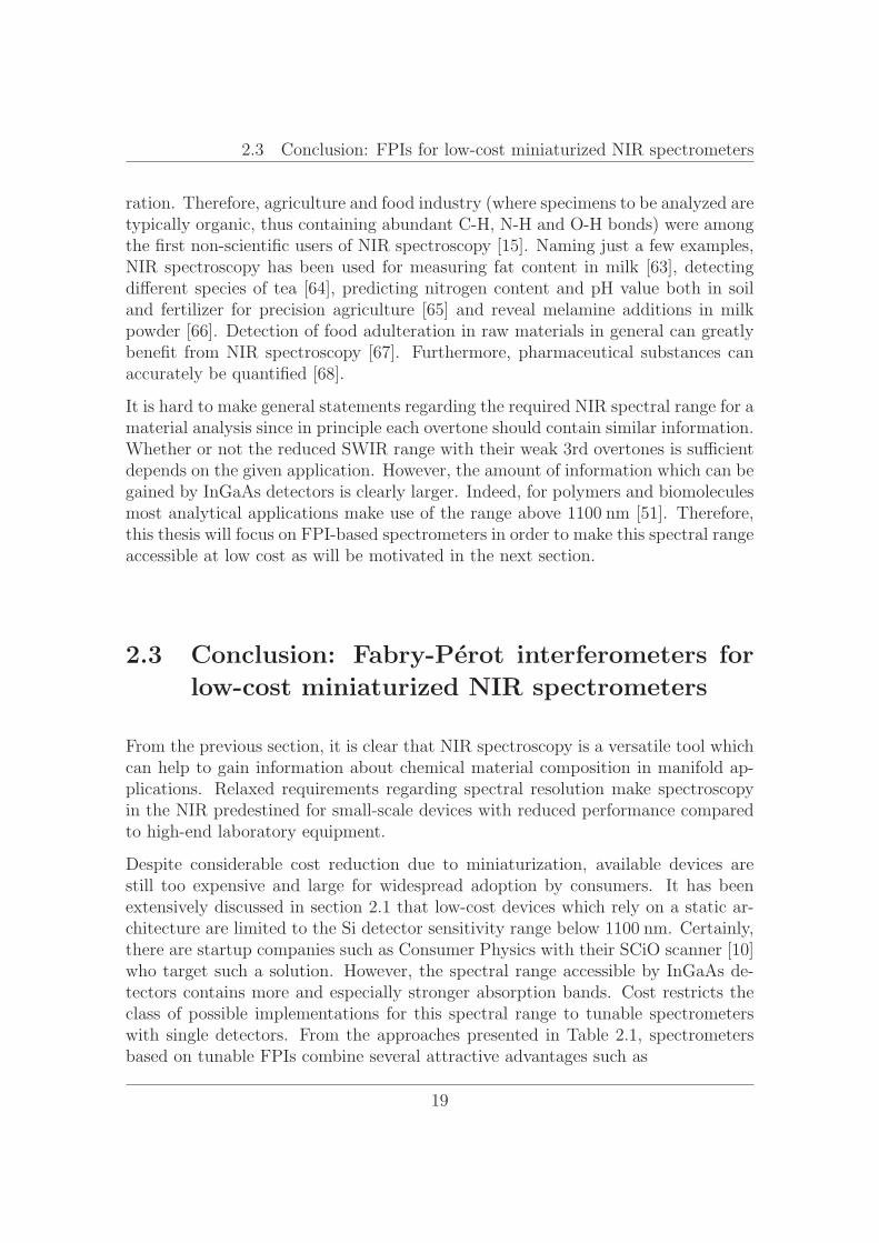
has been denoted explicitly as short wave infrared (SWIR)3. A detaileddiscussion of the listed devices is far outside the scope of this thesis. Therefore,only the most important aspects will be covered here and the reader is referred tothe cited literature and datasheets for further information. As an illustration of theworking principles, Fig. 2.2 provides schematic drawings of the different concepts.
Analogously to conventional laboratory spectrometers, a grating can be used asthe spectral element in combination with focusing optics to disperse the incidentspectrum in the spatial domain. For a fixed grating, an array detector placed inthe image plane then samples the spectrum at discrete positions (Fig. 2.2 (a)).This approach was pioneered by Ocean Optics in the 90s [4]. Nowadays, there arevarious other suppliers (Avantes, Wasatch Photonics, etc.) who offer cigar-box-sized, i.e., portable, fiber-coupled spectrometers. These devices are high-precisionscientific instruments available for a variety of spectral ranges at prices of severalthousand dollars. Miniaturization of grating spectrometers, e.g., by microoptics suchas nanoimprinted gratings on convex lenses have led to thumb-sized modules soldby Hamamatsu suitable for integration into mobile measurement equipment [37].
A grating, being a diffractive optical element, maps wavelength to diffraction angleso that a focusing element is necessary to focus the image located at infinity to thedetector plane. Therefore, at least one focal length of optical path is needed insidethe device. As a means to shrink spectrometer size, wavelength filters have beenintegrated directly on the detector. This can be achieved by a linear variable filter(LVF) which is essentially an FPI with a wedged shaped optical gap, thus possessingspatially varying transmittance (Fig. 2.2 (b)). Such a filter can directly be bonded toa linear detector array as it is done by Viavi for example [27]. Alternatively, a discretearray of interference filters (Fig. 2.2 (c)) can be integrated on a 2D imager resultingin compact devices with a height below . A popular example is the SCiO scannersold by Consumer Physics which raised two million dollars of crowdfunding in lessthan a month in 2014 [52]. Recently, integration of such a scanner in a smartphonehas been announced showing the enormous potential for miniaturization [53].
Apart from spectral elements with a bandpass behavior, static FT spectrometershave been proposed as well [28]. As an example, a Savart polariscope consistingof two birefringent crystals sandwiched between two polarizers can be used to mapOPD to transmission angle. A focusing lens then performs mapping to the spatialdomain which results in an interferogram on a 2D imager (Fig. 2.2 (d)).
3There is no consistent nomenclature regarding spectral ranges in the IR and the boundariesoften depend on the scientific field. For spectroscopy, it is common to subdivide MIR and NIR at. ( − ) since this is where the range of fundamental vibrations ends [51]. The further
division at . then stems from the silicon detector sensitivity limit.
11
Chapter 2. Overview of miniaturized spectrometers
Figure 2.2: Schematic representation of the static spectrometer concepts with array de-tectors listed in Table 2.1. Black boxes represent array detectors, colored arrows representlight of different wavelength.
Last, filter arrays with more complex transmission behavior than a bandpass filter(enabling a multiplex advantage to some extent but needing spectral reconstruction)have been demonstrated (Fig. 2.2 (e)). This was, e.g., achieved by an array ofcolloidal quantum dots of varying size dispensed on a detector [29]. Alternatively,nanostructured arrays exhibiting varying plasmonic resonances have been employed[40].
Despite these apparent differences in the spectral elements, the common principleof dispersing spectral information in space with subsequent detection by an arraydetector has certain consequences. Most importantly, it eliminates the need formoving components. Therefore, all of the aforementioned concepts remain staticafter assembly. This is a huge advantage in terms of ruggedness of a potentialproduct. In the simplest case, the components are aligned, glued and then maintaintheir calibration. Secondly, spectra can be taken in a snap-shot manner with allchannels illuminated at the same time instead of acquiring one channel after theother.
Regarding spectrometer size, the footprint cannot become smaller than the detectorarea. However, the most important drawback is related to the restrictions of thespectral range of detector sensitivity. While Si imagers are available at low cost dueto their widespread use as cameras in the visible range, other detector materialssuch as Ge and InGaAs are significantly more expensive. For example, a ”low-cost”256 pixel linear uncooled InGaAs detector costs several hundred dollars [54]. Thisis precisely why those spectrometers in Tab. 2.1 which aim at low-cost devices coveronly the SWIR spectral range up to approximately . Indeed, this is thetypical cut-off wavelength for silicon detectors given by the material’s band gap [55].
It cannot be excluded that these prices will drop in the future either due to anincreasing demand for infrared detectors or advances in semiconductor technology.However, until then spectrometers based on array detectors won’t be available abovethe silicon absorption edge at low cost. In section 2.2, it will be discussed that mole-
12
2.1 Categorization of miniaturized spectrometers by detector type
cular signatures in terms of absorption bands become weaker towards shorter wave-lengths. Therefore, the need to use silicon array detectors for low-cost applicationsimposes significant restrictions from a spectroscopic point of view.
2.1.3 Tunable spectrometers with single detectors
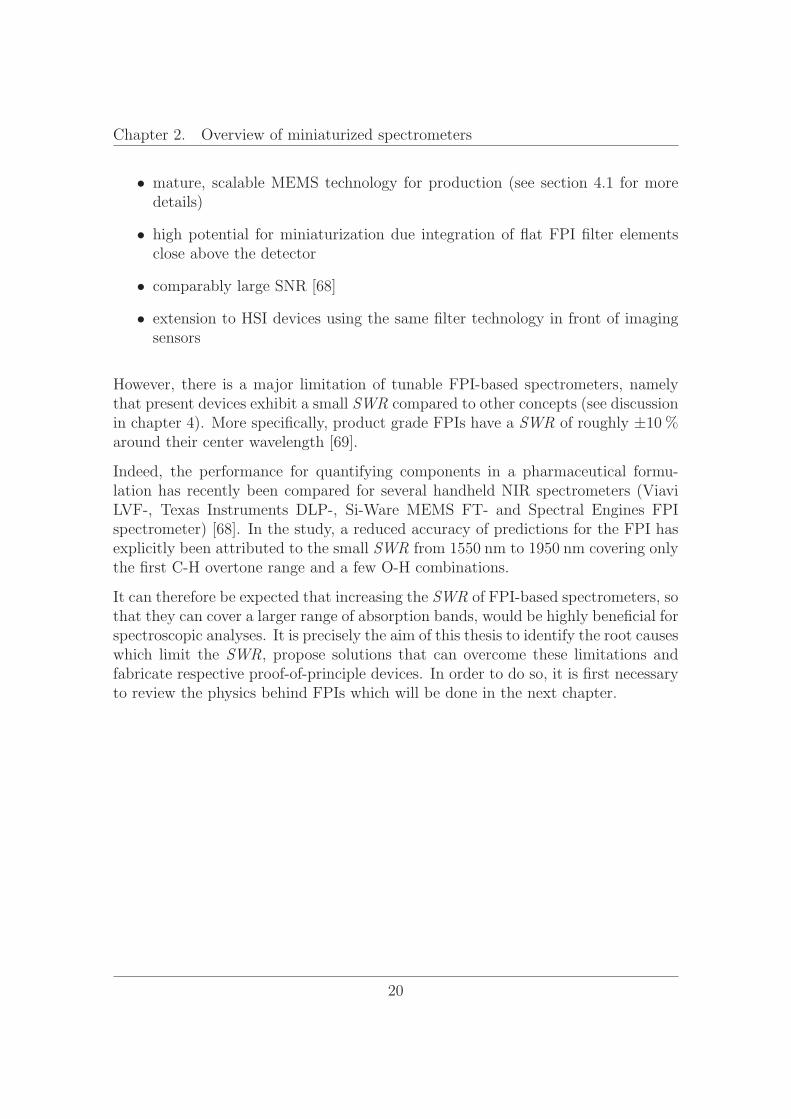
As discussed in section 2.1, spectrometers can also be realized with tunable spectralelements which provide spectral information in the temporal domain. Hence, themeasurement signal can be sampled with a single detector over time. Similar tothe previous subsection, several proposed or available miniaturized spectrometerswill first be presented following the overview in Table 2.1 with schematics shownin Fig. 2.3. A general discussion of common characteristics of these devices followsafterwards.
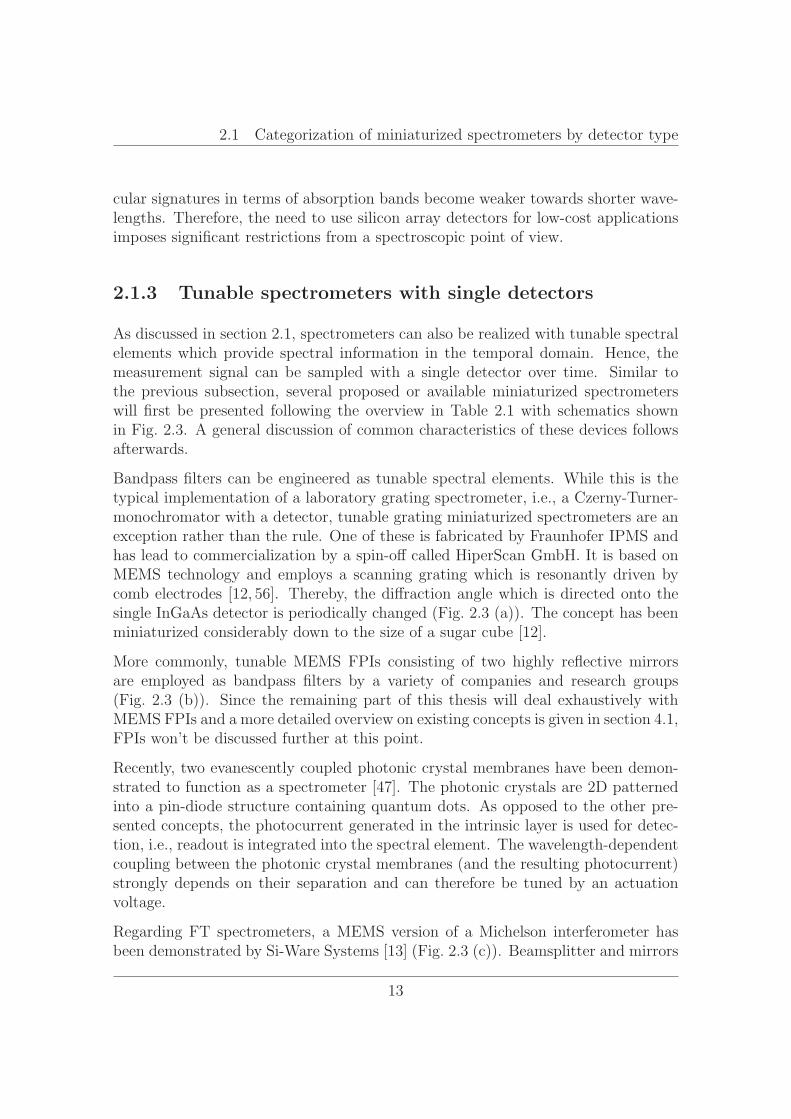
Bandpass filters can be engineered as tunable spectral elements. While this is thetypical implementation of a laboratory grating spectrometer, i.e., a Czerny-Turner-monochromator with a detector, tunable grating miniaturized spectrometers are anexception rather than the rule. One of these is fabricated by Fraunhofer IPMS andhas lead to commercialization by a spin-off called HiperScan GmbH. It is based onMEMS technology and employs a scanning grating which is resonantly driven bycomb electrodes [12, 56]. Thereby, the diffraction angle which is directed onto thesingle InGaAs detector is periodically changed (Fig. 2.3 (a)). The concept has beenminiaturized considerably down to the size of a sugar cube [12].
More commonly, tunable MEMS FPIs consisting of two highly reflective mirrorsare employed as bandpass filters by a variety of companies and research groups(Fig. 2.3 (b)). Since the remaining part of this thesis will deal exhaustively withMEMS FPIs and a more detailed overview on existing concepts is given in section 4.1,FPIs won’t be discussed further at this point.
Recently, two evanescently coupled photonic crystal membranes have been demon-strated to function as a spectrometer [47]. The photonic crystals are 2D patternedinto a pin-diode structure containing quantum dots. As opposed to the other pre-sented concepts, the photocurrent generated in the intrinsic layer is used for detec-tion, i.e., readout is integrated into the spectral element. The wavelength-dependentcoupling between the photonic crystal membranes (and the resulting photocurrent)strongly depends on their separation and can therefore be tuned by an actuationvoltage.
Regarding FT spectrometers, a MEMS version of a Michelson interferometer hasbeen demonstrated by Si-Ware Systems [13] (Fig. 2.3 (c)). Beamsplitter and mirrors
13
Chapter 2. Overview of miniaturized spectrometers
t
t
t tt
t
t
t
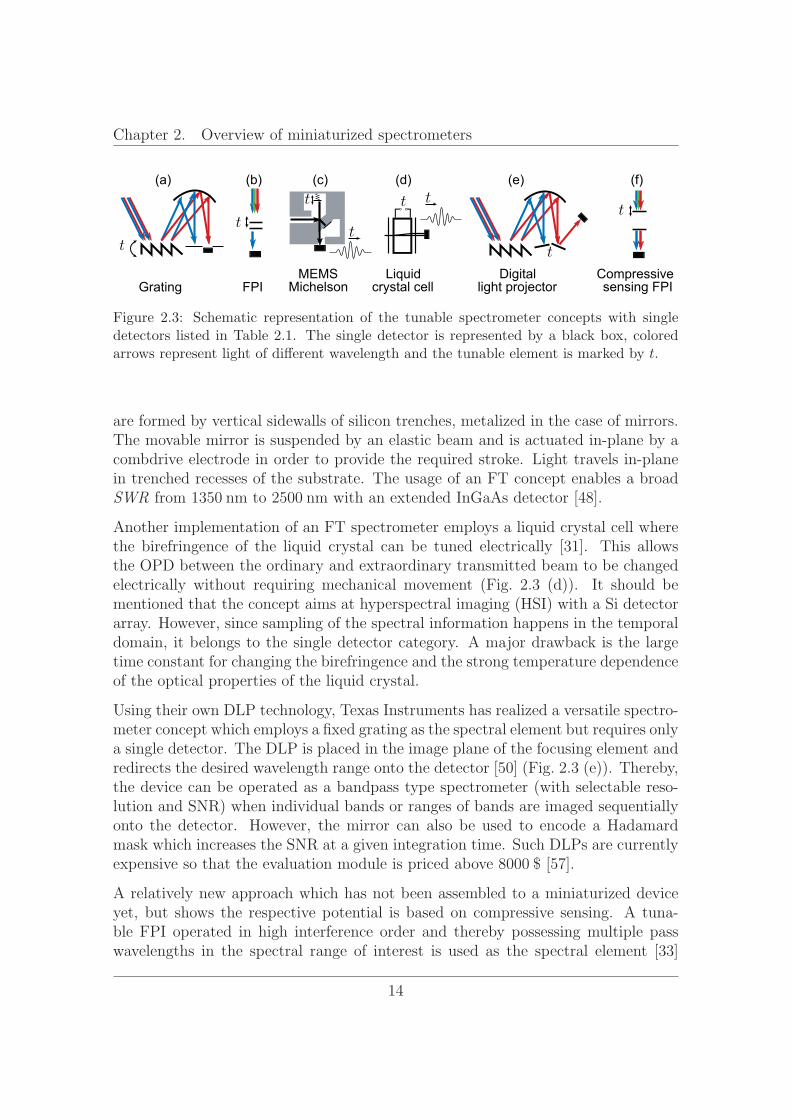
Figure 2.3: Schematic representation of the tunable spectrometer concepts with singledetectors listed in Table 2.1. The single detector is represented by a black box, coloredarrows represent light of different wavelength and the tunable element is marked by t.
are formed by vertical sidewalls of silicon trenches, metalized in the case of mirrors.The movable mirror is suspended by an elastic beam and is actuated in-plane by acombdrive electrode in order to provide the required stroke. Light travels in-planein trenched recesses of the substrate. The usage of an FT concept enables a broadSWR from to with an extended InGaAs detector [48].
Another implementation of an FT spectrometer employs a liquid crystal cell wherethe birefringence of the liquid crystal can be tuned electrically [31]. This allowsthe OPD between the ordinary and extraordinary transmitted beam to be changedelectrically without requiring mechanical movement (Fig. 2.3 (d)). It should bementioned that the concept aims at hyperspectral imaging (HSI) with a Si detectorarray. However, since sampling of the spectral information happens in the temporaldomain, it belongs to the single detector category. A major drawback is the largetime constant for changing the birefringence and the strong temperature dependenceof the optical properties of the liquid crystal.
Using their own DLP technology, Texas Instruments has realized a versatile spectro-meter concept which employs a fixed grating as the spectral element but requires onlya single detector. The DLP is placed in the image plane of the focusing element andredirects the desired wavelength range onto the detector [50] (Fig. 2.3 (e)). Thereby,the device can be operated as a bandpass type spectrometer (with selectable reso-lution and SNR) when individual bands or ranges of bands are imaged sequentiallyonto the detector. However, the mirror can also be used to encode a Hadamardmask which increases the SNR at a given integration time. Such DLPs are currentlyexpensive so that the evaluation module is priced above $ [57].
A relatively new approach which has not been assembled to a miniaturized deviceyet, but shows the respective potential is based on compressive sensing. A tuna-ble FPI operated in high interference order and thereby possessing multiple passwavelengths in the spectral range of interest is used as the spectral element [33]
14
2.1 Categorization of miniaturized spectrometers by detector type
(Fig. 2.3 (f)). Reconstruction of the incident spectrum is then achieved by themethods outlined in section 2.1.
Since all of the concepts described in this subsection only need a single detectorelement, they possess a cost advantage compared to array detector concepts in thosespectral ranges where detector area is the main cost driver in the spectrometersystem, i.e., in the NIR above the Si absorption edge. Therefore, most of them aredesigned for the NIR or longer wavelengths. Depending on the architecture, havingonly a single detector is also an advantage regarding the footprint of the device.
It should also be mentioned that among the scanning solutions, FPIs and liquidcrystal FT spectrometers can be used as filters for HSI. This is true if their aperturescan be fabricated large enough to be placed in front of an imager [31,42,58]. Thereby,the spectral dimension can be encoded in a hyperspectral datacube without loosingspatial resolution as it would be the case for HSI based on an array detector concept.
Nevertheless, there are also disadvantages related to tunable spectrometer concepts.Containing mechanically moving parts implies an increased amount of failure sourcescompared to static spectrometers. Drift of the device calibration over time alsoneeds to be considered more often than for static concepts. Last but not least,active tuning of the spectral element (possibly with feed back control) requires morecomplex electronics.
Apparently, none of the spectrometer concepts discussed here can be claimed to beuniquely superior to the others. The relative weight of the respective advantagesand disadvantages depends mainly on the target application. However, it can beconcluded that the intended spectral range can give a good indication for the detectortype if low cost is required. Cheap array detector solutions can at the momentonly be realized at wavelengths below where Si detectors are available.Above , detector area is an important cost driver favoring single detectorspectrometers.
Accordingly, a central question for every application of miniaturized spectrometers iswhich the part of the electromagnetic spectrum the desired information can be foundin. It turns out that the NIR between and is particularly suited formany practical applications as will be discussed in the following. Apparently, thisdoes not exclude neither single nor array detector concepts, so that a closer lookat this spectral range is required. The following section therefore aims at giving abasic understanding of the structure of NIR absorption spectra and highlights someof the possible applications which can be addressed by miniaturized spectrometers.
15
Chapter 2. Overview of miniaturized spectrometers
2.2 Principles of near infrared spectroscopy and
its applications
Absorption in the NIR spectral range ( - ) is dominated by so-calledovertones and combinations of fundamental vibrational excitations which reside inthe MIR. The origin of these absorption bands can best be understood by firstreviewing the interaction between a diatomic molecule and electromagnetic radiationin the simplest approximation. Overtones and combinations then follow when higherorders in the respective expansions are considered.
Absorption of a photon by a molecule requires a transition of the molecule from aninitial state ψ into an excited final state ψ in order to obey energy conversation.Within the so-called dipole approximation, the relevant matrix element in Fermi’sGolden Rule which determines the transition rate Γ→ is given by [59]
Γ→ ∝∣∣∣∣∫ ψ∗Mψ
∣∣∣∣2 , (2.1)
where M is the dipole moment operator. The frequency ν, that the respectivetransition absorbs photons at, is ν = (E − E )/h, where E and E are the energylevels of final and initial state, respectively and h is Planck’s constant.
As a first approximation, the atomic potential for small displacements x aroundthe equilibrium position can be regarded as harmonic so that the orthogonal basisfor the wave function ψ are Hermite polynomials Hn(x), where n is the polynomialorder.
The dipole moment can be expanded as a Taylor series M(x) = M0 + M1x +0.5 ·M2x
2+ ... where Mj denotes the j-th derivate of M with respect to x. Due tothe recursive relation of Hermite polynomials
xHn(x) =1
2Hn+1(x) + nHn−1(x), (2.2)
the j-th expansion order in the Taylor series for M couples Hermite polynomialsdiffering in order by Δn = j in the matrix element Eq. 2.1. Therefore, if M(x)was only a linear function in x, absorption would only take place at a frequencyν0 corresponding to the energetic difference between the equi-spaced energy levelsof the harmonic oscillator. This so-called fundamental transition lies in the MIRspectral range.
Absorption bands in the NIR now stem from taking into account higher orders in theapproximations above [51]. Anharmonicity in the atomic potential consequently re-sults in the basis functions not being pure Hermite polynomials but a superposition.
16
2.2 Principles of near infrared spectroscopy and its applications
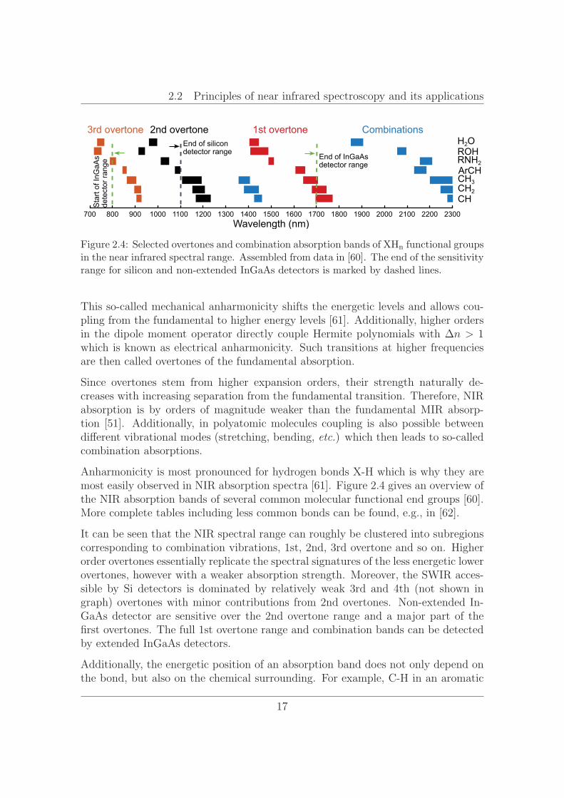
700 800 900 1000 1100 1200 1300 1400 1500 1600 1700 1800 1900 2000 2100 2200 2300Wavelength (nm)
CH3CH2CH
H2OROHRNH2ArCH
Combinations1st overtone2nd overtone3rd overtoneEnd of silicondetector range
End of InGaAsdetector range
Sta
rt of
InG
aAs
dete
ctor
rang
e
Figure 2.4: Selected overtones and combination absorption bands of functional groupsin the near infrared spectral range. Assembled from data in [60]. The end of the sensitivityrange for silicon and non-extended InGaAs detectors is marked by dashed lines.
This so-called mechanical anharmonicity shifts the energetic levels and allows cou-pling from the fundamental to higher energy levels [61]. Additionally, higher ordersin the dipole moment operator directly couple Hermite polynomials with Δn > 1which is known as electrical anharmonicity. Such transitions at higher frequenciesare then called overtones of the fundamental absorption.
Since overtones stem from higher expansion orders, their strength naturally de-creases with increasing separation from the fundamental transition. Therefore, NIRabsorption is by orders of magnitude weaker than the fundamental MIR absorp-tion [51]. Additionally, in polyatomic molecules coupling is also possible betweendifferent vibrational modes (stretching, bending, etc.) which then leads to so-calledcombination absorptions.
Anharmonicity is most pronounced for hydrogen bonds X-H which is why they aremost easily observed in NIR absorption spectra [61]. Figure 2.4 gives an overview ofthe NIR absorption bands of several common molecular functional end groups [60].More complete tables including less common bonds can be found, e.g., in [62].
It can be seen that the NIR spectral range can roughly be clustered into subregionscorresponding to combination vibrations, 1st, 2nd, 3rd overtone and so on. Higherorder overtones essentially replicate the spectral signatures of the less energetic lowerovertones, however with a weaker absorption strength. Moreover, the SWIR acces-sible by Si detectors is dominated by relatively weak 3rd and 4th (not shown ingraph) overtones with minor contributions from 2nd overtones. Non-extended In-GaAs detector are sensitive over the 2nd overtone range and a major part of thefirst overtones. The full 1st overtone range and combination bands can be detectedby extended InGaAs detectors.
Additionally, the energetic position of an absorption band does not only depend onthe bond, but also on the chemical surrounding. For example, C-H in an aromatic
17
Chapter 2. Overview of miniaturized spectrometers
molecule absorbs at different wavelengths than it is the case for C-H in aliphaticcompounds [61].
These principles regarding the origin of NIR absorption have some important conse-quences for applications. First, due to the reduced absorption coefficient, NIR radi-ation has a significantly larger penetration depth in materials compared to stronglyabsorbed MIR radiation [15]. Therefore, long path lengths are possible in transmis-sion measurement configuration, i.e., larger samples can be used for measurement.Furthermore, measurement of diffuse reflectance from scattering and absorption deepin the bulk of a sample is possible without being too sensitive to the surface. This isan advantage for measurements on natural products such as fruits or grains wherethe skin or peel is of less interest compared to the inside [4]. It also means thatmeasurements can be conducted non-destructively on solid samples.
Additionally, for an inhomogeneous sample a long path length essentially leads toaveraging the absorption over a large volume. Therefore, NIR measurements arerelatively independent of the actual measurement position reducing necessary effortsfor sample preparation. This also explains why NIR spectroscopy is particularlypopular for natural products which are inherently inhomogeneous [4]. However, itshould be noted that weak absorption also leads to a lower limit for detection in therange of . to . Accordingly, trace components such as allergens are likely tobe undetectable [6].
If the sample is inhomogeneous, the bonds contributing to NIR absorption are typ-ically present in a range of different chemical environments. Therefore, spectralfeatures are significantly broadened compared to sharply resolved vibration spec-tra in the MIR. Accordingly, resolution requirements for NIR spectrometers arerather moderate. For example, resolution is sufficient for many analyseson natural products [4] and moisture detection can be performed at even lowerresolution [15]. The possibility to gain valuable information without needing highperformance equipment makes the NIR particularly attractive for miniaturized spec-trometers.
Due to the large number of possible overtones and overlapping broad spectral fea-tures, NIR spectra are typically smooth with only few clearly resolved features.Compared to the MIR, where certain vibrational contributions can clearly be iden-tified by their absorption peak position, it is almost impossible to interpret NIRspectra manually. Therefore, computational multivariate data analysis techniquessuch as principal component analysis for classification or partial least-squares re-gression for quantification are typically used [15,61].
The aforementioned characteristics make NIR spectroscopy a preferred method wheninhomogeneous samples need to be analyzed rapidly without extensive sample prepa-
18
2.3 Conclusion: FPIs for low-cost miniaturized NIR spectrometers
ration. Therefore, agriculture and food industry (where specimens to be analyzed aretypically organic, thus containing abundant C-H, N-H and O-H bonds) were amongthe first non-scientific users of NIR spectroscopy [15]. Naming just a few examples,NIR spectroscopy has been used for measuring fat content in milk [63], detectingdifferent species of tea [64], predicting nitrogen content and pH value both in soiland fertilizer for precision agriculture [65] and reveal melamine additions in milkpowder [66]. Detection of food adulteration in raw materials in general can greatlybenefit from NIR spectroscopy [67]. Furthermore, pharmaceutical substances canaccurately be quantified [68].
It is hard to make general statements regarding the required NIR spectral range for amaterial analysis since in principle each overtone should contain similar information.Whether or not the reduced SWIR range with their weak 3rd overtones is sufficientdepends on the given application. However, the amount of information which can begained by InGaAs detectors is clearly larger. Indeed, for polymers and biomoleculesmost analytical applications make use of the range above [51]. Therefore,this thesis will focus on FPI-based spectrometers in order to make this spectral rangeaccessible at low cost as will be motivated in the next section.
2.3 Conclusion: Fabry-Perot interferometers for
low-cost miniaturized NIR spectrometers
From the previous section, it is clear that NIR spectroscopy is a versatile tool whichcan help to gain information about chemical material composition in manifold ap-plications. Relaxed requirements regarding spectral resolution make spectroscopyin the NIR predestined for small-scale devices with reduced performance comparedto high-end laboratory equipment.
Despite considerable cost reduction due to miniaturization, available devices arestill too expensive and large for widespread adoption by consumers. It has beenextensively discussed in section 2.1 that low-cost devices which rely on a static ar-chitecture are limited to the Si detector sensitivity range below . Certainly,there are startup companies such as Consumer Physics with their SCiO scanner [10]who target such a solution. However, the spectral range accessible by InGaAs de-tectors contains more and especially stronger absorption bands. Cost restricts theclass of possible implementations for this spectral range to tunable spectrometerswith single detectors. From the approaches presented in Table 2.1, spectrometersbased on tunable FPIs combine several attractive advantages such as
19
Chapter 2. Overview of miniaturized spectrometers
• mature, scalable MEMS technology for production (see section 4.1 for moredetails)
• high potential for miniaturization due integration of flat FPI filter elementsclose above the detector
• comparably large SNR [68]
• extension to HSI devices using the same filter technology in front of imagingsensors
However, there is a major limitation of tunable FPI-based spectrometers, namelythat present devices exhibit a small SWR compared to other concepts (see discussionin chapter 4). More specifically, product grade FPIs have a SWR of roughly ±around their center wavelength [69].
Indeed, the performance for quantifying components in a pharmaceutical formu-lation has recently been compared for several handheld NIR spectrometers (ViaviLVF-, Texas Instruments DLP-, Si-Ware MEMS FT- and Spectral Engines FPIspectrometer) [68]. In the study, a reduced accuracy of predictions for the FPI hasexplicitly been attributed to the small SWR from to covering onlythe first C-H overtone range and a few O-H combinations.
It can therefore be expected that increasing the SWR of FPI-based spectrometers, sothat they can cover a larger range of absorption bands, would be highly beneficial forspectroscopic analyses. It is precisely the aim of this thesis to identify the root causeswhich limit the SWR, propose solutions that can overcome these limitations andfabricate respective proof-of-principle devices. In order to do so, it is first necessaryto review the physics behind FPIs which will be done in the next chapter.
20
Chapter 3
Fundamentals of Fabry-Perotinterferometers
The Fabry-Perot interferometer as such has been known for over a century [70]and without doubt ranks among the most influential optical devices in modernphysics [71]. Since its invention, FPIs or more generally speaking high-finesse Fabry-Perot cavities have found numerous applications starting from resolving the hyper-fine structure of atomic emissions [71, 72] in the early 20th century. Later on, theywere employed as laser resonators while nowadays there are also used to study light-matter interaction in modern cavity quantum electrodynamics (QED) [73,74].
Due to its high importance at least a basic analytical description is contained in mosttextbooks on optics [75,76]. For most applications, FPIs are designed as high-finessecavities which are operated at a high interference order. In this thesis, however, atunable bandpass filter with moderate resolution but broad SWR is needed (seediscussion in the previous chapter). This mode of operation differs to some extentfrom the aforementioned usage since it requires both a lower interference order andfinesse. Therefore, this chapter introduces the fundamentals of FPIs with specialfocus on these aspects. Another excellent introduction to the topic regarding MEMSFPIs can be found in [77].
Starting from the theoretical concept of an ideal FPI, the basic formulae are reviewedin section 3.1 both as a reference for the reader and for introducing the notation usedin this work. Subsequently, deviations from the ideal case in a real interferometerand their influence on transmittance will be discussed in section 3.2 since theirexperimental characterization will play a central role in chapter 7. The chapterends with a description of FPIs based on distributed Bragg reflectors (DBRs) insection 3.3 as they are the type of mirror which is used in this thesis.
21
Chapter 3. Fundamentals of Fabry-Perot interferometers
3.1 The ideal Fabry-Perot interferometer (FPI)
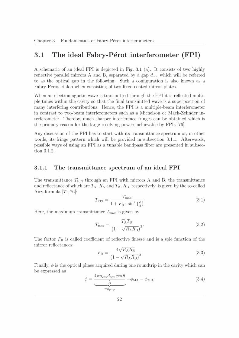
A schematic of an ideal FPI is depicted in Fig. 3.1 (a). It consists of two highlyreflective parallel mirrors A and B, separated by a gap d which will be referredto as the optical gap in the following. Such a configuration is also known as aFabry-Perot etalon when consisting of two fixed coated mirror plates.
When an electromagnetic wave is transmitted through the FPI it is reflected multi-ple times within the cavity so that the final transmitted wave is a superposition ofmany interfering contributions. Hence, the FPI is a multiple-beam interferometerin contrast to two-beam interferometers such as a Michelson or Mach-Zehnder in-terferometer. Thereby, much sharper interference fringes can be obtained which isthe primary reason for the large resolving powers achievable by FPIs [76].
Any discussion of the FPI has to start with its transmittance spectrum or, in otherwords, its fringe pattern which will be provided in subsection 3.1.1. Afterwards,possible ways of using an FPI as a tunable bandpass filter are presented in subsec-tion 3.1.2.
3.1.1 The transmittance spectrum of an ideal FPI
The transmittance T through an FPI with mirrors A and B, the transmittanceand reflectance of which are TA, RA and TB, RB, respectively, is given by the so-calledAiry-formula [71,76]:
T =T
1 + F · 2(φ2
) (3.1)
Here, the maximum transmittance T is given by
T =TATB(
1−√RARB
)2 . (3.2)
The factor F is called coefficient of reflective finesse and is a sole function of themirror reflectances:
F =4√R R(
1−√R R
)2 (3.3)
Finally, φ is the optical phase acquired during one roundtrip in the cavity which canbe expressed as
φ =4πn d θ
λ︸ ︷︷ ︸=φ
−φMA − φMB, (3.4)
22
3.1 The ideal Fabry-Perot interferometer (FPI)
T
T T T
θ
R R
R R
T
d
Figure 3.1: (a) Schematic representation of an ideal FPI and propagation of light in a rayoptics picture. (b) Corresponding transmittance spectra depending on the optical phaseacquired in one cavity round trip assuming two ideal mirrors for different values of theirreflectance R.
where n is the refractive index in the cavity1, θ is the angle of incidence andλ is the incident wavelength. These quantities determine the phase shift due tolight propagation in the cavity φ . Additionally, φMA,MB is the phase shift uponreflection at mirror A and B, respectively. For the sake of simplicity, the phase shiftupon reflectance will be neglected at the moment (φ = φ ) but its influence willbe discussed in detail in subsection 3.3.2.
In the commonly studied special case of absorptionless equal mirrors (T = T = T ;R = R = R;R + T = 1), the prefactor reduces to T = 1 and the reflectivefinesse becomes F = 4R/(1−R)2. Fig. 3.1 (b) shows a plot of T (φ) for differentmirror reflectances R. The transmittance spectrum T (φ) has 2π periodicity2 withmaxima (also called interference fringes) occurring whenever the sine vanishes, i.e.,for every integer interference order m with
φm = 2πm. (3.5)
This case corresponds to full constructive interference of the partially transmittedwaves. The separation between consecutive fringes is termed free spectral range(FSR) and is constant in phase space, namely 2π, independent of mirror reflectance.
Minima occur at φm = 2πm + π (destructive interference) with a transmittance ofT = (1 + F )−1. The contrast C is then defined as
C :=T
T= 1 + F . (3.6)
1In this thesis, the medium in the cavity will always be air, so that n ≈ 1.2Some books use φ′ = φ/2 as their definition for the phase which then results in π periodicity.
23
Chapter 3. Fundamentals of Fabry-Perot interferometers
Accordingly, higher mirror reflectance R leads to stronger suppression between theinterference fringes. Furthermore, the peak width expressed as the full width at halfmaximum (FWHM ) is also a function of F and can be expressed as3:
FWHM =4√F
(3.7)
In the limiting case of R → 1, F diverges and the transmittance spectrum becomesa series of delta peaks. Mirrors with reflectance below unity impose a less stringentrestriction on the transmitted phase and therefore lead to broader transmittancepeaks. The reflective finesse F of the cavity is defined as the ratio between FSRand FWHM , i.e., it is a measure for the number of resolvable fringes within oneFSR. F is therefore given by
F :=FSR
FWHM=π
2
√F . (3.8)
A fringe pattern as it is shown in Fig. 3.1 (b) appears, whenever φ (d , n , θ, λ)is varied by one of its parameters while keeping the remaining parameters fixed.The parameter which is varied determines the type of usage of the device. Forexample, the dominant configuration used to examine hyperfine splitting in atomicemission spectra in the early 20th century consisted of fixed etalon plates with afocusing lens placed thereafter and a photographic plate in its focal plane [78]. Whenilluminated with (quasi)-monochromatic light, the phase difference due to differentincident angles leads to a fringe pattern on the photographic plate.4 It was onlyrealized around the middle of the 20th century that the FPI can be used as a highresolution band pass filter to build tunable spectrometers with a single detector aswill be discussed in the next subsection [78].
3.1.2 Tunable FPIs as filters for spectrometers
When used as a spectrometer, white light is incident on the FPI so that λ is variedover a certain range of wavelengths. A fringe pattern in wavelength space appearsfor fixed d , n and θ, i.e., transmittance occurs for every wavelength λm thatcan interfere constructively. The interference condition for constructive interferencein Eq. 3.5 then reads
λm =2n d θ
m. (3.9)
3Since typically F � 1 applies, (φ/2) ≈ φ/2 holds in the vicinity of the interference fringewhere the transmittance drops to 0.5.
4Following the nomenclature of the previous chapter, this essentially is a configuration withfixed spectral element and spatially extended detector.
24
3.1 The ideal Fabry-Perot interferometer (FPI)
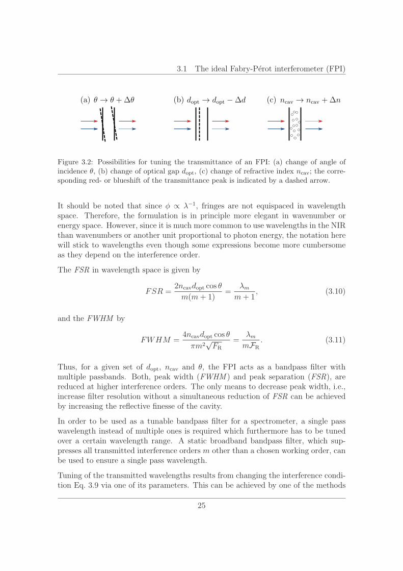
θ → θ +Δθ d → d −Δd n → n +Δn(a) (b) (c)
Figure 3.2: Possibilities for tuning the transmittance of an FPI: (a) change of angle ofincidence θ, (b) change of optical gap d , (c) change of refractive index n ; the corre-sponding red- or blueshift of the transmittance peak is indicated by a dashed arrow.
It should be noted that since φ ∝ λ−1, fringes are not equispaced in wavelengthspace. Therefore, the formulation is in principle more elegant in wavenumber orenergy space. However, since it is much more common to use wavelengths in the NIRthan wavenumbers or another unit proportional to photon energy, the notation herewill stick to wavelengths even though some expressions become more cumbersomeas they depend on the interference order.
The FSR in wavelength space is given by
FSR =2n d θ
m(m+ 1)=
λmm+ 1
, (3.10)
and the FWHM by
FWHM =4n d θ
πm2√F
=λmmF . (3.11)
Thus, for a given set of d , n and θ, the FPI acts as a bandpass filter withmultiple passbands. Both, peak width (FWHM ) and peak separation (FSR), arereduced at higher interference orders. The only means to decrease peak width, i.e.,increase filter resolution without a simultaneous reduction of FSR can be achievedby increasing the reflective finesse of the cavity.
In order to be used as a tunable bandpass filter for a spectrometer, a single passwavelength instead of multiple ones is required which furthermore has to be tunedover a certain wavelength range. A static broadband bandpass filter, which sup-presses all transmitted interference orders m other than a chosen working order, canbe used to ensure a single pass wavelength.
Tuning of the transmitted wavelengths results from changing the interference condi-tion Eq. 3.9 via one of its parameters. This can be achieved by one of the methods
25
Chapter 3. Fundamentals of Fabry-Perot interferometers
depicted in Fig. 3.2. These include changing the angle of incidence θ by tiltingthe etalon, changing the optical gap d by displacement of one of the mirrors orchanging the refractive index n by, e.g., changing the pressure of an enclosed gas.
Resolution of a such a spectrometer then depends on the peak FWHM of the choseninterference order and the SWR cannot exceed the respective FSR. Consequently,a higher working interference order m leads to better resolution at the expense ofSWR according to Eqs. 3.11 and 3.10. The SWR is further limited by how far thetransmitted peak can spectrally be tuned within its FSR. While all of the methodsdepicted in Fig. 3.2 have been used historically [79], only a change of the opticalgap d provides both, a sufficient change of the optical phase for a large SWR andcompatibility with MEMS manufacturing as described in chapter 4.
Explicitly, if a SWR with Δλ = λ , −λ , is given and an interferenceorderm is chosen, the optical gap has to be tuned by Δd = mΔλ /2. When thedispersion of the phase shift upon reflection at the FPI mirrors φ , is consideredas well in subsection 3.3.2, this tuning range Δd will always become larger.
It has been mentioned before that one of the main advantages of an FPI comparedto two-beam interferometric devices is that the large number of interfering rays canlead to very high resolution. Therefore, in its typical applications, e.g., as a lasercavity, the Fabry-Perot cavity is designed for high resolution over a specific, limitedwavelength range. From Eq. 3.10 and Eq. 3.11 and the discussion above it becomesobvious that in order to reach this high resolution such devices need very high mirrorreflectance R in the vicinity of the working wavelength and can be operated in highinterference order m. The simultaneous reduction of FSR is of minor importance.
It has been discussed in section 2.2 that for NIR spectroscopy, the requirementsregarding spectrometer resolution for resolving vibrational overtones are moderate(FWHM ≈ ). However, an NIR spectrometer benefits greatly from a largeSWR. Therefore, FPIs in miniaturized spectrometers typically work in low inter-ference order and need less reflective mirrors which, however, reflect over a broadspectral range. Some of the resulting consequences will be addressed in the followingsections.
3.2 Peak broadening in a real FPI
In the previous section, the ideal FPI has been introduced as an arrangement ofperfectly parallel mirrors (d = .), which, when illuminated by collimatedlight (θ = .) imposes a strict interference condition on the incident light. Inpractice, mirrors are not perfectly parallel and the incident light is not perfectly
26
3.2 Peak broadening in a real FPI
collimated [80]. The last point is especially true when considering a handheld devicefor analyzing diffuse reflectance from a sample object.
Accordingly, a distribution of d and θ contributes to the interference condition inEq. 3.9 which can then be fulfilled by a range of wavelengths, i.e., the transmittancepeak broadens. The effect of these non-idealities on the FPI transmittance will bediscussed in this section. Subsection 3.2.1 introduces the concept of an effectivefinesse F which can be used to describe peak broadening for various types of non-idealities. Subsection 3.2.2 then explains the implications for an optimally designedFPI under the presence of defects.
3.2.1 Types of defects and their contribution to the effectivefinesse
Deviations from the ideal FPI configuration are commonly referred to as defects.Generally speaking, any kind of defect leads to a phase distribution G(φ) withfinite width, so that the effective transmittance T , of the FPI is given as theconvolution [80–82]
T , =
∫T (φ′) ·G (φ− φ′) φ′, (3.12)
with T being the ideal FPI transmittance from Eq. 3.1. If G(φ) has a finite width,i.e., in the presence of defects, T , will consequently be broader than T . It canbe shown that for practical reflectances found in an FPI the effective width of thebroadened transmittance FWHM can be calculated using [81]
FWHM2 = FWHM2 + FWHM2 , (3.13)
where FWHM is the width of the defect distribution G(φ). An important con-sequence is that FWHM is always larger than its individual components so thatthe defect contribution may become the dominant broadening factor for high mirrorreflectances [78].
Just as a reflective finesse F can be assigned to the ideal cavity with FWHM ∝ F−1,a defect finesse F can be used to describe additional broadening due to defects.The real FPI can then approximately be described by an effective finesse F obeying
F−2 = F−2 +∑j
F−2,j, (3.14)
27
Chapter 3. Fundamentals of Fabry-Perot interferometers
F = λ2d
F = λ√3d
F = λ√22d
F = 2mθ2
d d d
θ
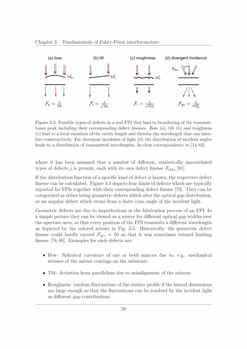
Figure 3.3: Possible types of defects in a real FPI that lead to broadening of the transmit-tance peak including their corresponding defect finesses. Bow (a), tilt (b) and roughness(c) lead to a local variation of the cavity length and thereby the wavelength that can inter-fere constructively. For divergent incidence of light (d) the distribution of incident anglesleads to a distribution of transmitted wavelengths. In close correspondence to [14,83].
where it has been assumed that a number of different, statistically uncorrelatedtypes of defects j is present, each with its own defect finesse F ,j [81].
If the distribution function of a specific kind of defect is known, the respective defectfinesse can be calculated. Figure 3.3 depicts four kinds of defects which are typicallyreported for FPIs together with their corresponding defect finesse [79]. They can becategorized as either being geometric defects which alter the optical gap distribution,or an angular defect which stems from a finite cone angle of the incident light.
Geometric defects are due to imperfections in the fabrication process of an FPI. Ina simple picture they can be viewed as a source for different optical gap widths overthe aperture area, so that every position of the FPI transmits a different wavelengthas depicted by the colored arrows in Fig. 3.3. Historically, the geometric defectfinesse could hardly exceed F = 50 so that it was sometimes termed limitingfinesse [78,80]. Examples for such defects are:
• Bow: Spherical curvature of one or both mirrors due to, e.g., mechanicalstresses of the mirror coatings on the substrate
• Tilt: deviation from parallelism due to misalignment of the mirrors
• Roughness: random fluctuations of the surface profile if the lateral dimensionsare large enough so that the fluctuations can be resolved by the incident lightas different gap contributions
28
3.2 Peak broadening in a real FPI
It will be discussed in subsection 4.1.1 that for MEMS FPIs, bow and tilt are ofmajor importance and it is one of the main tasks for the MEMS design to ensure ahigh defect finesse.
It should be noted that the defect finesses for all geometric defects are of the formF ,j = bj · λ
djwhere dj is the characteristic optical gap variation due to the re-
spective defect and bj is a constant which is related to the distribution functionunderlying the defect. In that sense, geometric defects are more detrimental theshorter the operating wavelength is, i.e., the better the wavelength can resolve thedefect.
An angular defect due to a divergent incidence is less dependent on the actual FPIbut rather on the whole optical system that the FPI is used in. As an example,the incident angle can be controlled by a pinhole of controllable size followed bya collimating lens. Due to φ ∝ θ larger angles of incidence lead to a blueshift of the transmittance wavelength. Therefore, the transmittance spectrum atnormal divergent incidence with a half cone angle θ is blue-shifted compared tothe collimated normal incidence case.
The corresponding defect finesse is F = 2mθ2
and depends inversely on the inter-
ference order m so that low order interferometers as they will be used in this thesisare less sensitive to divergent incidence.
It should be noted that at large angles of incidence, not only the broadening dueto the phase distribution has to be taken into account. Additionally, a shift of thereflector characteristic as well as splitting of the transmission responses for the s-and p-polarized components of the incident light have to be considered. However, insuch cases F would be impractically low so that they are of no practical relevancefor FPI operation.
3.2.2 Optimization of integral transmittance in the presenceof defects
For handheld spectrometer applications as described in chapter 2, signal intensitylevels at a detector behind the filter can be low due to non-defined illumination andoptical path configurations. This can be problematic in terms of the achievable SNR.The detected signal is essentially a spectral integral of the transmitted spectrumaccording to Fig. 2.1. In order to maximize SNR at a given resolution, one thereforeseeks to maximize integral transmittance at a given FWHM .
In principle, the optical throughput of the filter (and thus SNR) can be increased
29
Chapter 3. Fundamentals of Fabry-Perot interferometers
by increasing filter area A or the accepted interval of incident angles. However, asdiscussed in the last subsection, an increased cone angle θ of the incident lightdirectly reduces the divergence finesse. Furthermore, geometric defects such as bowand tilt typically scale with filter area A so that the respective geometric defectfinesse also decreases. Accordingly, when increasing throughput by these methods,defect finesses will at one point limit the achievable effective finesse.
If the effective finesse is defect-limited, the actual mirror reflectance is irrelevantfor filter resolution. However, the detected signal level and thus the SNR can stillbenefit from a useful choice of mirrors. The reasoning can be shown by simpleconsideration of, e.g., a tilted FPI with different mirror reflectances.
In case of such a geometric defect (i.e. a variation of the optical gap within the aper-ture area) the transmittance T through the full FPI can be calculated numericallyas an area integral over local ideal FPI transmittances T (d (r)) [77, 84]
T = 1/A
∫A
T (d (r))dA, (3.15)
which is essentially equivalent to the convolution in Eq. 3.12. This requires theassumption that the gap variation is small compared to the lateral dimensions ofthe FPI so that the FPI can locally be regarded as an ideal FPI with parallel mirrors.It will be shown in chapter 7 that this is the case for the FPIs in this thesis.
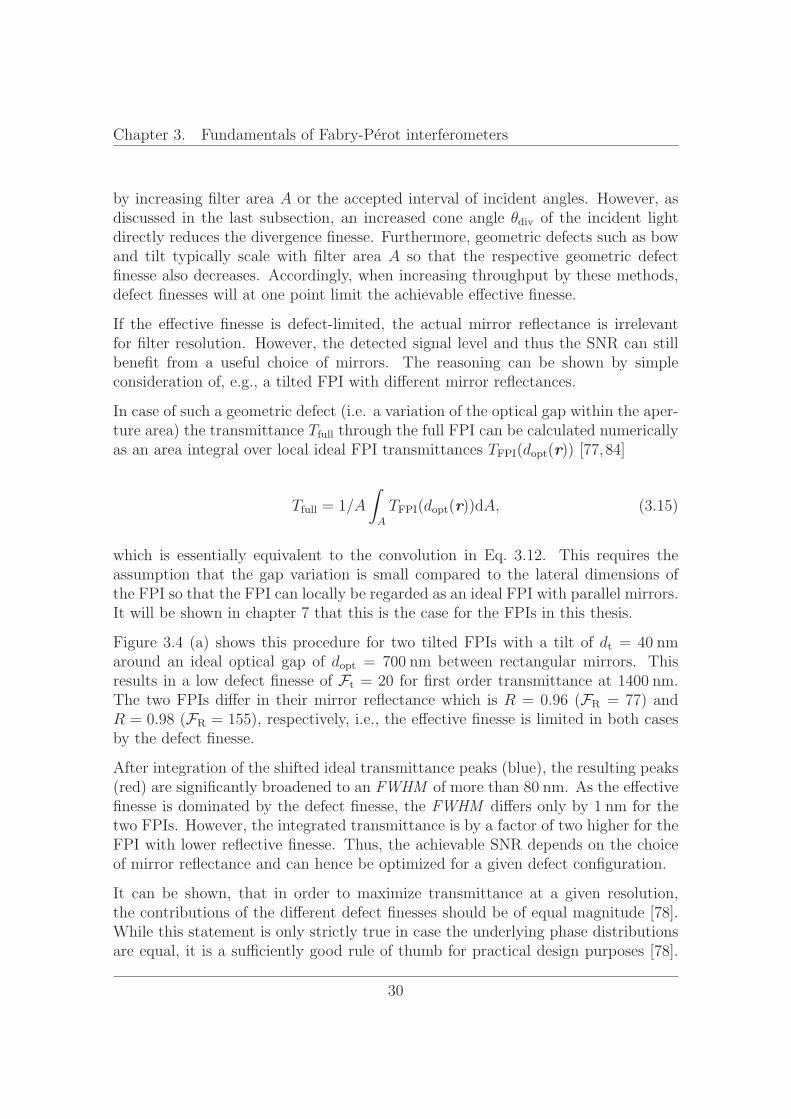
Figure 3.4 (a) shows this procedure for two tilted FPIs with a tilt of d =around an ideal optical gap of d = between rectangular mirrors. Thisresults in a low defect finesse of F = 20 for first order transmittance at .The two FPIs differ in their mirror reflectance which is R = 0.96 (F = 77) andR = 0.98 (F = 155), respectively, i.e., the effective finesse is limited in both casesby the defect finesse.
After integration of the shifted ideal transmittance peaks (blue), the resulting peaks(red) are significantly broadened to an FWHM of more than . As the effectivefinesse is dominated by the defect finesse, the FWHM differs only by for thetwo FPIs. However, the integrated transmittance is by a factor of two higher for theFPI with lower reflective finesse. Thus, the achievable SNR depends on the choiceof mirror reflectance and can hence be optimized for a given defect configuration.
It can be shown, that in order to maximize transmittance at a given resolution,the contributions of the different defect finesses should be of equal magnitude [78].While this statement is only strictly true in case the underlying phase distributionsare equal, it is a sufficiently good rule of thumb for practical design purposes [78].
30
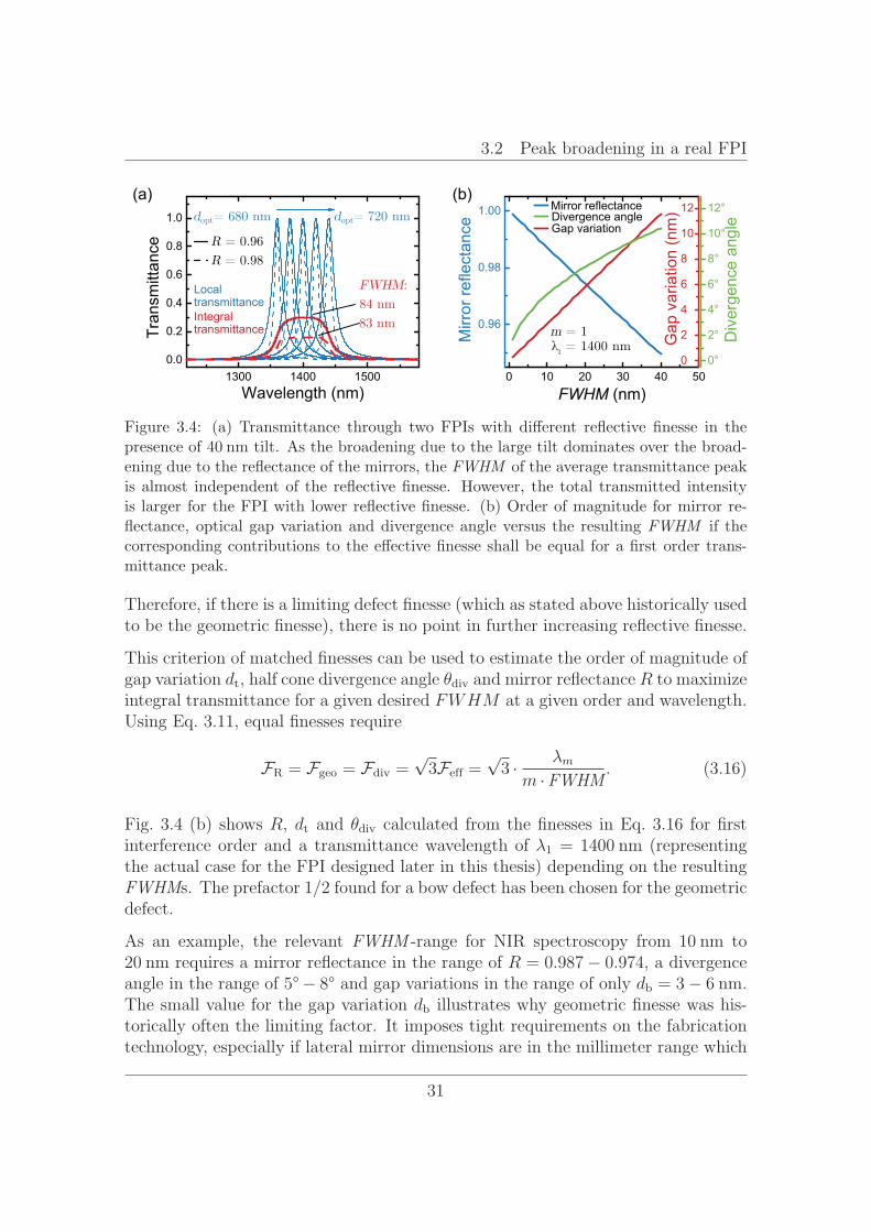
3.2 Peak broadening in a real FPI
1300 1400 15000.0
0.2
0.4
0.6
0.8
1.0
:84 nm83 nm
= 0.96= 0.98
Tran
smitt
ance
Wavelength (nm)
= 680 nm = 720 nm
LocaltransmittanceIntegraltransmittance
(a)
Figure 3.4: (a) Transmittance through two FPIs with different reflective finesse in thepresence of tilt. As the broadening due to the large tilt dominates over the broad-ening due to the reflectance of the mirrors, the FWHM of the average transmittance peakis almost independent of the reflective finesse. However, the total transmitted intensityis larger for the FPI with lower reflective finesse. (b) Order of magnitude for mirror re-flectance, optical gap variation and divergence angle versus the resulting FWHM if thecorresponding contributions to the effective finesse shall be equal for a first order trans-mittance peak.
Therefore, if there is a limiting defect finesse (which as stated above historically usedto be the geometric finesse), there is no point in further increasing reflective finesse.
This criterion of matched finesses can be used to estimate the order of magnitude ofgap variation d , half cone divergence angle θ and mirror reflectance R to maximizeintegral transmittance for a given desired FWHM at a given order and wavelength.Using Eq. 3.11, equal finesses require
F = F = F =√3F =
√3 · λmm ·FWHM
. (3.16)
Fig. 3.4 (b) shows R, d and θ calculated from the finesses in Eq. 3.16 for firstinterference order and a transmittance wavelength of λ1 = (representingthe actual case for the FPI designed later in this thesis) depending on the resultingFWHMs. The prefactor 1/2 found for a bow defect has been chosen for the geometricdefect.
As an example, the relevant FWHM -range for NIR spectroscopy from torequires a mirror reflectance in the range of R = 0.987− 0.974, a divergence
angle in the range of 5 − 8 and gap variations in the range of only d = − .The small value for the gap variation d illustrates why geometric finesse was his-torically often the limiting factor. It imposes tight requirements on the fabricationtechnology, especially if lateral mirror dimensions are in the millimeter range which
31
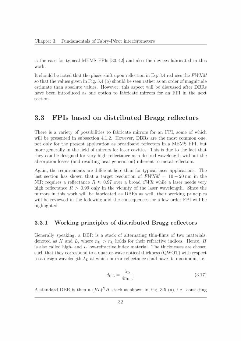
Chapter 3. Fundamentals of Fabry-Perot interferometers
is the case for typical MEMS FPIs [30, 42] and also the devices fabricated in thiswork.
It should be noted that the phase shift upon reflection in Eq. 3.4 reduces the FWHMso that the values given in Fig. 3.4 (b) should be seen rather as an order of magnitudeestimate than absolute values. However, this aspect will be discussed after DBRshave been introduced as one option to fabricate mirrors for an FPI in the nextsection.
3.3 FPIs based on distributed Bragg reflectors
There is a variety of possibilities to fabricate mirrors for an FPI, some of whichwill be presented in subsection 4.1.2. However, DBRs are the most common one,not only for the present application as broadband reflectors in a MEMS FPI, butmore generally in the field of mirrors for laser cavities. This is due to the fact thatthey can be designed for very high reflectance at a desired wavelength without theabsorption losses (and resulting heat generation) inherent to metal reflectors.
Again, the requirements are different here than for typical laser applications. Thelast section has shown that a target resolution of FWHM = − in theNIR requires a reflectance R ≈ 0.97 over a broad SWR while a laser needs veryhigh reflectance R > 0.99 only in the vicinity of the laser wavelength. Since themirrors in this work will be fabricated as DBRs as well, their working principleswill be reviewed in the following and the consequences for a low order FPI will behighlighted.
3.3.1 Working principles of distributed Bragg reflectors
Generally speaking, a DBR is a stack of alternating thin-films of two materials,denoted as H and L, where n > n holds for their refractive indices. Hence, His also called high- and L low-refractive index material. The thicknesses are chosensuch that they correspond to a quarter-wave optical thickness (QWOT) with respectto a design wavelength λ at which mirror reflectance shall have its maximum, i.e.,
d , =λ
4n ,
. (3.17)
A standard DBR is then a (HL)NH stack as shown in Fig. 3.5 (a), i.e., consisting
32
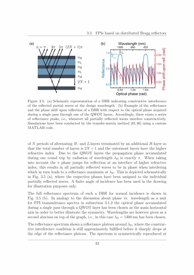
3.3 FPIs based on distributed Bragg reflectors
nH
nH
nH
nH
nL
nL
2N + 1
φ = π 3π 5π (2N + 1)π
0.5 1.0 1.5
0.0
0.5
1.0
Wavelength (nm)
Ref
lect
ance
Optical phase (rad)
1300 650 433
0.5
1.0
1.5
2.0
Pha
se s
hift
upon
refl.
(rad
)
max
(b)
Figure 3.5: (a) Schematic representation of a DBR indicating constructive interferenceof the reflected partial waves at the design wavelength. (b) Example of the reflectanceand the phase shift upon reflection of a DBR with respect to the optical phase acquiredduring a single pass through one of the QWOT layers. Accordingly, there exists a seriesof reflectance peaks, i.e., whenever all partially reflected waves interfere constructively.Simulations have been conducted by the transfer-matrix method [85, 86] using a customMATLAB code.
of N periods of alternating H - and L-layers terminated by an additional H -layer sothat the total number of layers is 2N + 1 and the outermost layers have the higherrefractive index. Due to the QWOT layers the propagation phase accumulatedduring one round trip by radiation of wavelength λ is exactly π. When takinginto account the π phase jumps for reflection at an interface of higher refractiveindex, this results in all partially reflected waves to be in phase when interferingwhich in turn leads to a reflectance maximum at λ . This is depicted schematicallyin Fig. 3.5 (a), where the respective phases have been assigned to the individualpartially reflected waves. A finite angle of incidence has been used in the drawingfor illustration purposes only.
The full reflectance spectrum of such a DBR for normal incidence is shown inFig. 3.5 (b). In analogy to the discussion about phase vs. wavelength as a unitfor FPI transmittance spectra in subsection 3.1.2 the optical phase accumulatedduring a single pass through a QWOT layer has been chosen as the main horizontalaxis in order to better illustrate the symmetry. Wavelengths are however given as asecond abscissa on top of the graph, i.e., in this case λ = has been chosen.
The reflectance spectrum shows a reflectance plateau around λ , where the construc-tive interference condition is still approximately fulfilled before it sharply drops atthe edge of the reflectance plateau. The spectrum is symmetrically reproduced at
33
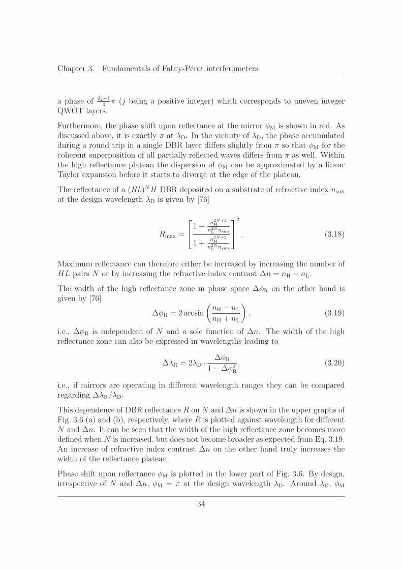
Chapter 3. Fundamentals of Fabry-Perot interferometers
a phase of 2j−14π (j being a positive integer) which corresponds to uneven integer
QWOT layers.
Furthermore, the phase shift upon reflectance at the mirror φ is shown in red. Asdiscussed above, it is exactly π at λ . In the vicinity of λ , the phase accumulatedduring a round trip in a single DBR layer differs slightly from π so that φ for thecoherent superposition of all partially reflected waves differs from π as well. Withinthe high reflectance plateau the dispersion of φ can be approximated by a linearTaylor expansion before it starts to diverge at the edge of the plateau.
The reflectance of a (HL)NH DBR deposited on a substrate of refractive index nat the design wavelength λ is given by [76]
R =
⎡⎣1− n2N+2
n2Nn
1 +n2N+2
n2Nn
⎤⎦2
. (3.18)
Maximum reflectance can therefore either be increased by increasing the number ofHL pairs N or by increasing the refractive index contrast Δn = n − n .
The width of the high reflectance zone in phase space Δφ on the other hand isgiven by [76]
Δφ = 2
(n − n
n + n
), (3.19)
i.e., Δφ is independent of N and a sole function of Δn. The width of the highreflectance zone can also be expressed in wavelengths leading to
Δλ = 2λ · Δφ
1−Δφ2, (3.20)
i.e., if mirrors are operating in different wavelength ranges they can be comparedregarding Δλ /λ .
This dependence of DBR reflectance R on N and Δn is shown in the upper graphs ofFig. 3.6 (a) and (b), respectively, where R is plotted against wavelength for differentN and Δn. It can be seen that the width of the high reflectance zone becomes moredefined whenN is increased, but does not become broader as expected from Eq. 3.19.An increase of refractive index contrast Δn on the other hand truly increases thewidth of the reflectance plateau.
Phase shift upon reflectance φ is plotted in the lower part of Fig. 3.6. By design,irrespective of N and Δn, φ = π at the design wavelength λ . Around λ , φ
34
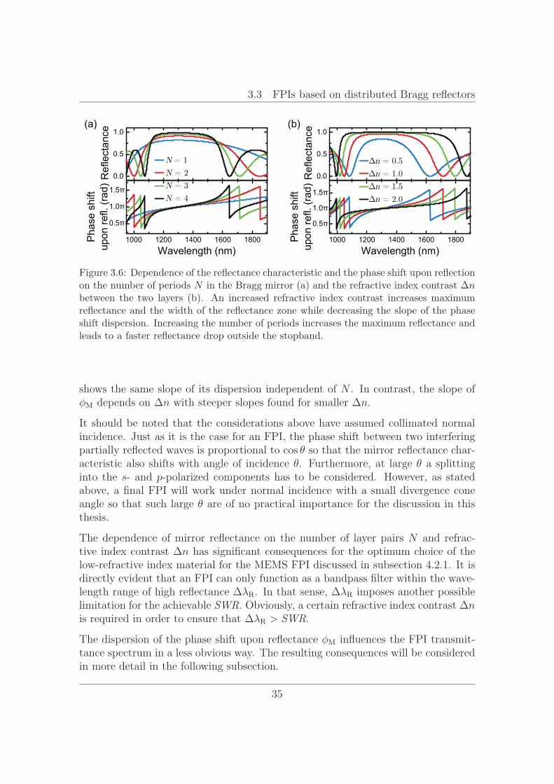
3.3 FPIs based on distributed Bragg reflectors
0.0
0.5
1.0
1000 1200 1400 1600 1800
0.5
1.0
1.5
= 1= 2= 3= 4
Ref
lect
ance
Pha
se s
hift
upon
refl.
(rad
)
Wavelength (nm)
(a)
0.0
0.5
1.0
1000 1200 1400 1600 1800
0.5
1.0
1.5
Ref
lect
ance
Pha
se s
hift
upon
refl.
(rad
)
Wavelength (nm)
(b)
Figure 3.6: Dependence of the reflectance characteristic and the phase shift upon reflectionon the number of periods N in the Bragg mirror (a) and the refractive index contrast Δnbetween the two layers (b). An increased refractive index contrast increases maximumreflectance and the width of the reflectance zone while decreasing the slope of the phaseshift dispersion. Increasing the number of periods increases the maximum reflectance andleads to a faster reflectance drop outside the stopband.
shows the same slope of its dispersion independent of N . In contrast, the slope ofφ depends on Δn with steeper slopes found for smaller Δn.
It should be noted that the considerations above have assumed collimated normalincidence. Just as it is the case for an FPI, the phase shift between two interferingpartially reflected waves is proportional to θ so that the mirror reflectance char-acteristic also shifts with angle of incidence θ. Furthermore, at large θ a splittinginto the s- and p-polarized components has to be considered. However, as statedabove, a final FPI will work under normal incidence with a small divergence coneangle so that such large θ are of no practical importance for the discussion in thisthesis.
The dependence of mirror reflectance on the number of layer pairs N and refrac-tive index contrast Δn has significant consequences for the optimum choice of thelow-refractive index material for the MEMS FPI discussed in subsection 4.2.1. It isdirectly evident that an FPI can only function as a bandpass filter within the wave-length range of high reflectance Δλ . In that sense, Δλ imposes another possiblelimitation for the achievable SWR. Obviously, a certain refractive index contrast Δnis required in order to ensure that Δλ > SWR.
The dispersion of the phase shift upon reflectance φ influences the FPI transmit-tance spectrum in a less obvious way. The resulting consequences will be consideredin more detail in the following subsection.
35
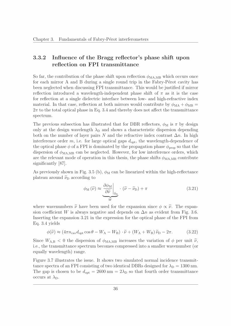
Chapter 3. Fundamentals of Fabry-Perot interferometers
3.3.2 Influence of the Bragg reflector’s phase shift uponreflection on FPI transmittance
So far, the contribution of the phase shift upon reflection φ , which occurs oncefor each mirror A and B during a single round trip in the Fabry-Perot cavity hasbeen neglected when discussing FPI transmittance. This would be justified if mirrorreflection introduced a wavelength-independent phase shift of π as it is the casefor reflection at a single dielectric interface between low- and high-refractive indexmaterial. In that case, reflection at both mirrors would contribute by φ + φ =2π to the total optical phase in Eq. 3.4 and thereby does not affect the transmittancespectrum.
The previous subsection has illustrated that for DBR reflectors, φ is π by designonly at the design wavelength λ and shows a characteristic dispersion dependingboth on the number of layer pairs N and the refractive index contrast Δn. In highinterference order m, i.e. for large optical gaps d , the wavelength-dependence ofthe optical phase φ of a FPI is dominated by the propagation phase φ so that thedispersion of φ , can be neglected. However, for low interference orders, whichare the relevant mode of operation in this thesis, the phase shifts φ , contributesignificantly [87].
As previously shown in Fig. 3.5 (b), φ can be linearized within the high-reflectanceplateau around ν according to
φ (ν) ≈ ∂φ
∂ν
∣∣∣∣ν︸ ︷︷ ︸
W
· (ν − ν ) + π (3.21)
where wavenumbers ν have been used for the expansion since φ ∝ ν. The expan-sion coefficient W is always negative and depends on Δn as evident from Fig. 3.6.Inserting the expansion 3.21 in the expression for the optical phase of the FPI fromEq. 3.4 yields
φ(ν) ≈ (4πn d θ −W −W ) · ν + (W +W ) ν − 2π. (3.22)
Since W , < 0 the dispersion of φ , increases the variation of φ per unit ν,i.e., the transmittance spectrum becomes compressed into a smaller wavenumber (orequally wavelength) range.
Figure 3.7 illustrates the issue. It shows two simulated normal incidence transmit-tance spectra of an FPI consisting of two identical DBRs designed for λ = .The gap is chosen to be d = = 2λ so that fourth order transmittanceoccurs at λ .
36
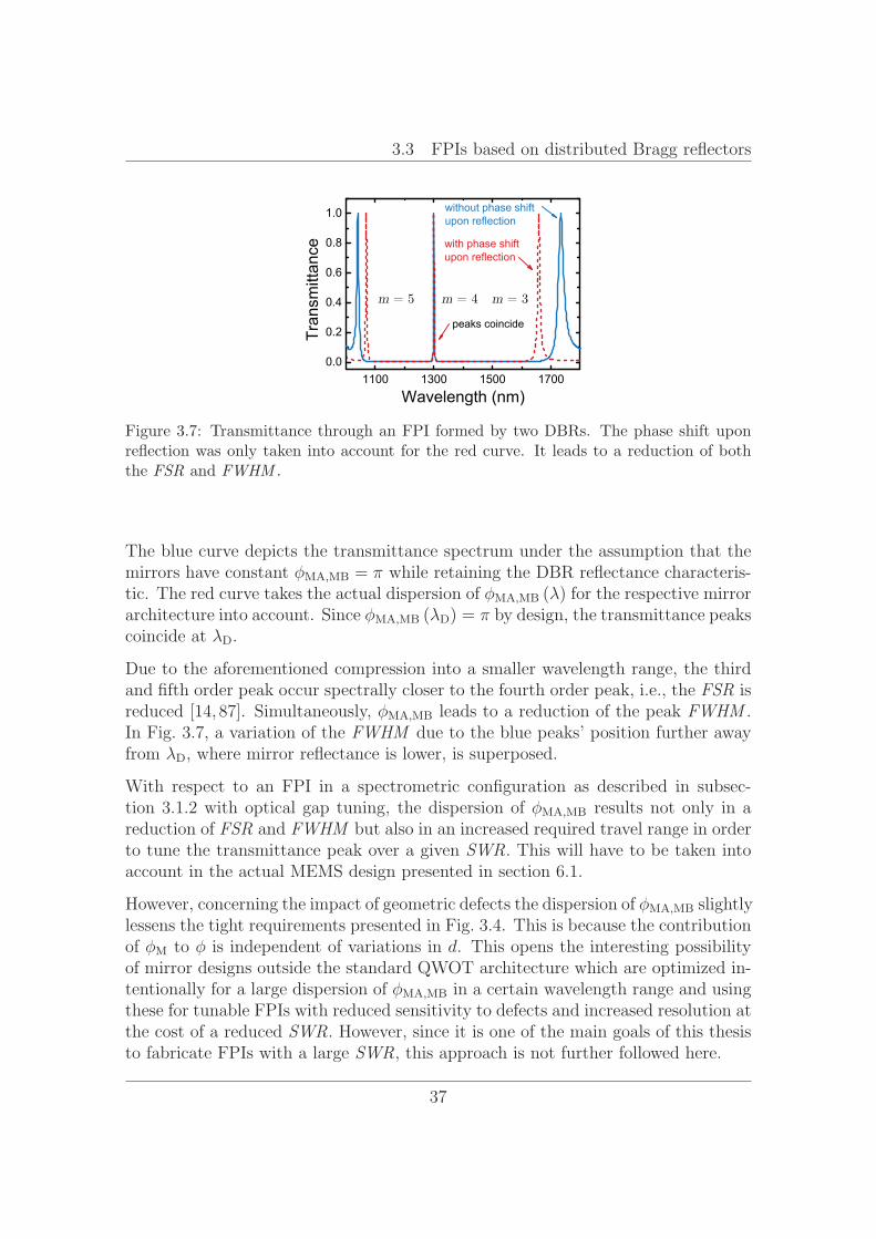
3.3 FPIs based on distributed Bragg reflectors
1100 1300 1500 17000.0
0.2
0.4
0.6
0.8
1.0
with phase shiftupon reflection
Tran
smitt
ance
Wavelength (nm)
without phase shiftupon reflection
peaks coincide
Figure 3.7: Transmittance through an FPI formed by two DBRs. The phase shift uponreflection was only taken into account for the red curve. It leads to a reduction of boththe FSR and FWHM .
The blue curve depicts the transmittance spectrum under the assumption that themirrors have constant φ , = π while retaining the DBR reflectance characteris-tic. The red curve takes the actual dispersion of φ , (λ) for the respective mirrorarchitecture into account. Since φ , (λ ) = π by design, the transmittance peakscoincide at λ .
Due to the aforementioned compression into a smaller wavelength range, the thirdand fifth order peak occur spectrally closer to the fourth order peak, i.e., the FSR isreduced [14, 87]. Simultaneously, φ , leads to a reduction of the peak FWHM .In Fig. 3.7, a variation of the FWHM due to the blue peaks’ position further awayfrom λ , where mirror reflectance is lower, is superposed.
With respect to an FPI in a spectrometric configuration as described in subsec-tion 3.1.2 with optical gap tuning, the dispersion of φ , results not only in areduction of FSR and FWHM but also in an increased required travel range in orderto tune the transmittance peak over a given SWR. This will have to be taken intoaccount in the actual MEMS design presented in section 6.1.
However, concerning the impact of geometric defects the dispersion of φ , slightlylessens the tight requirements presented in Fig. 3.4. This is because the contributionof φ to φ is independent of variations in d. This opens the interesting possibilityof mirror designs outside the standard QWOT architecture which are optimized in-tentionally for a large dispersion of φ , in a certain wavelength range and usingthese for tunable FPIs with reduced sensitivity to defects and increased resolution atthe cost of a reduced SWR. However, since it is one of the main goals of this thesisto fabricate FPIs with a large SWR, this approach is not further followed here.
37
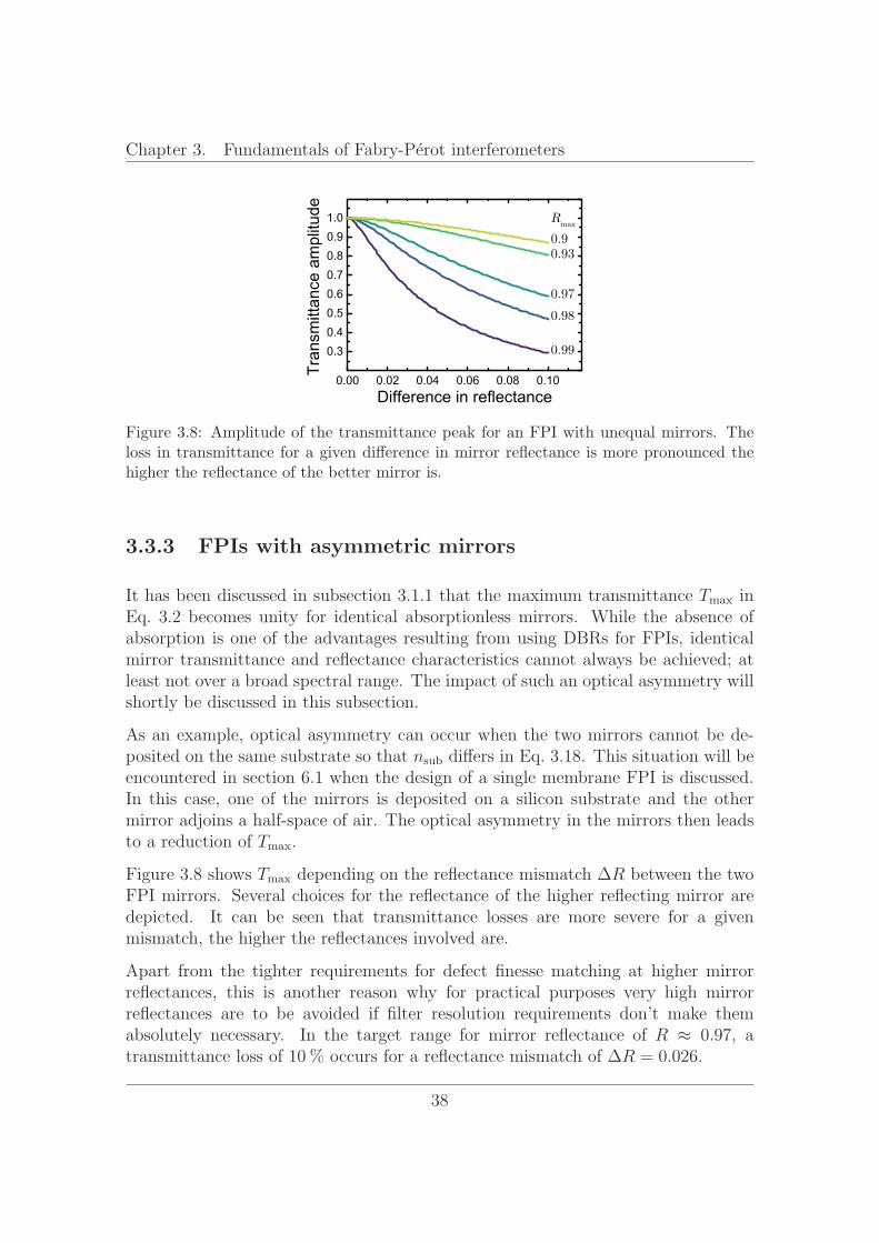
Chapter 3. Fundamentals of Fabry-Perot interferometers
0.00 0.02 0.04 0.06 0.08 0.10
0.30.40.50.60.70.80.91.0
Tran
smitt
ance
am
plitu
de
Difference in reflectance
Figure 3.8: Amplitude of the transmittance peak for an FPI with unequal mirrors. Theloss in transmittance for a given difference in mirror reflectance is more pronounced thehigher the reflectance of the better mirror is.
3.3.3 FPIs with asymmetric mirrors
It has been discussed in subsection 3.1.1 that the maximum transmittance T inEq. 3.2 becomes unity for identical absorptionless mirrors. While the absence ofabsorption is one of the advantages resulting from using DBRs for FPIs, identicalmirror transmittance and reflectance characteristics cannot always be achieved; atleast not over a broad spectral range. The impact of such an optical asymmetry willshortly be discussed in this subsection.
As an example, optical asymmetry can occur when the two mirrors cannot be de-posited on the same substrate so that n differs in Eq. 3.18. This situation will beencountered in section 6.1 when the design of a single membrane FPI is discussed.In this case, one of the mirrors is deposited on a silicon substrate and the othermirror adjoins a half-space of air. The optical asymmetry in the mirrors then leadsto a reduction of T .
Figure 3.8 shows T depending on the reflectance mismatch ΔR between the twoFPI mirrors. Several choices for the reflectance of the higher reflecting mirror aredepicted. It can be seen that transmittance losses are more severe for a givenmismatch, the higher the reflectances involved are.
Apart from the tighter requirements for defect finesse matching at higher mirrorreflectances, this is another reason why for practical purposes very high mirrorreflectances are to be avoided if filter resolution requirements don’t make themabsolutely necessary. In the target range for mirror reflectance of R ≈ 0.97, atransmittance loss of occurs for a reflectance mismatch of ΔR = 0.026.
38
3.4 Summary: Low-order FPIs for tunable filters with broad SWR
As a consequence, in section 6.1 an optical MEMS design with fully symmetricmirrors will be proposed which prevents such transmittance losses.
3.4 Summary: Low-order FPIs for tunable filters
with broad spectral working range
Summing up, the fundamentals behind the transmittance spectra of FPIs, both inthe theoretically ideal configuration and in the realistic case under the presence ofdefects, have been explained in this chapter. Given the previous discussion, it canbe concluded that a concept suitable for manufacturing FPIs with a broad SWR inthe NIR and a resolution in the range of FWHM = − needs to provide orenable the following:
• Mirrors with a broad high reflectance zone Δλ , since SWR ≤ Δλ . There-fore, a material combination with sufficient Δn is required if DBRs are used asmirrors. A reflectance of roughly R ≈ 0.97 is optimal for matching reflectivefinesse to defect finesses.
• Interferometer operation in first interference order for maximizing the FSR,since SWR ≤ FSR. Hence, positioning of the mirrors with a separation in theorder of half the transmitted wavelength is necessary.
• An actuator capable of displacing at least one of the mirrors in order to changed by Δd ≥ (λ , − λ , )/2. The phase shift upon reflectancedetermines the actual Δd for a given choice of mirrors. Mirror displacementmust be controllable with nanometer precision in order to accurately determinethe transmitted wavelength.
• Parallelism between the mirrors with deviations not exceeding the nanometerrange.
As already stated above, these values have to be seen as rough estimates for therequirements which will be detailed in the following chapters. There are additionalboundary conditions such as a limitation of the angle of incidence θ to a cone withhalf angle in a range between ◦ and ◦. This, however, is a requirement for thefull optical system rather than the FPI alone. Similarly, the minimum mirror areawhich provides sufficient optical throughput is a critical parameter but depends onexternal factors such as the illumination conditions and the detector type.
39

Chapter 3. Fundamentals of Fabry-Perot interferometers
One possible fabrication platform is microfabricating FPIs as MEMS devices. Thenext chapter is therefore devoted to the discussion of the suitability of MEMS tech-nology to meet the requirements stated above. This will eventually allow to deriveMEMS-specific solution approaches to be tested within this thesis.
40
Chapter 4
Broadband near infrared MEMSFabry-Perot interferometers:Opportunities and challenges
As discussed in the previous chapters, it is highly desirably to build FPIs workingin first interference order to maximize their SWR and thereby increase the numberof potential applications. However, this imposes tight requirements on the chosenfabrication technology. As shown in chapter 3, it must first provide mirrors with asufficiently large width of their high reflectance zone Δλ . Second, the mirrors mustbe displaced with respect to each other with nanometer precision while maintaininga high degree of parallelism. Above all, these requirements have to be met at smalldevice dimensions and low cost.
MEMS technology offers the advantage of providing mature deposition techniquesenabling mirror fabrication with nanometer control of the individual layer thick-nesses as well as established types of actuators allowing mirror movement to be pre-cisely controlled. Furthermore, MEMS fabrication favors planar device geometriessuch as an FPI due to large-area material deposition and subsequent structuring byphotolithography and anisotropic etching. Hence, batch fabrication of many deviceson a single substrate is possible, which in turn reduces unit price. Therefore, MEMSFPIs have been a research topic starting around the late 1980s [88] with increasingactivity in recent years [89].
This chapter starts with an overview of the state of the art of MEMS FPIs insection 4.1. Differences between published designs are highlighted and the resultingadvantages and disadvantages for device performance are addressed. Based on thisdiscussion and knowledge from previous chapters, current limitations for the SWR
41
Chapter 4. Broadband NIR MEMS FPIs: Opportunities and challenges
as well as the parallelism between the FPI mirrors in surface-micromachined FPIsare pointed out in section 4.2. Subsequently, in section 4.3, a solution strategy forcircumventing these limitations is proposed both regarding the choice of materialsand device architecture. This defines the research questions for this work which willbe answered during the remaining chapters of this thesis.
4.1 State of the art of MEMS FPIs
Over the last years, MEMS FPI designs covering different subranges of the elec-tromagnetic spectrum from the UV [90] to the thermal infrared (TIR) [91] havebeen demonstrated. Their maturity ranges from research samples [46, 90], to pack-aged filters [16, 30] with a detector and full spectrometer modules including a lightsource [11] or even a battery and cloud connectivity [92].
The actual design is often a direct consequence of the chosen spectral range, e.g.,because absorption may limit the choice of available substrates and mirror materialsor because achievable layer thicknesses may be limited by technological constraints.Simply speaking, it is impossible to propose an ideal FPI design which is suitablefor all wavelength ranges.
However, state-of-the-art MEMS FPIs can be categorized with respect to both theirmicromachining platform and their mirror design independent of their target SWR.The first point leads to the comparison between surface- and bulk-micromachinedFPI concepts in subsection 4.1.1. These share respective advantages and disadvan-tages and therefore impose certain architectural constraints which will briefly bediscussed.
Next, a short discussion of possible types of mirror designs follows in subsection 4.1.2.
Finally, some of the designs including their performance indicators which have beenpublished in literature will be analyzed more closely in subsection 4.1.3. This alsoserves as an overview which the performance of the proposed and fabricated devicesin this thesis can be benchmarked against. An excellent introduction to the topiccan also be found in [77,89].
4.1.1 Surface vs. bulk micromachining approaches
MEMS FPIs can be fabricated either by following a surface- or bulk micromachiningapproach. In surface micromachining, thin films are deposited onto a substrate,typically a silicon wafer, and subsequently patterned by lithography and anisotropic
42
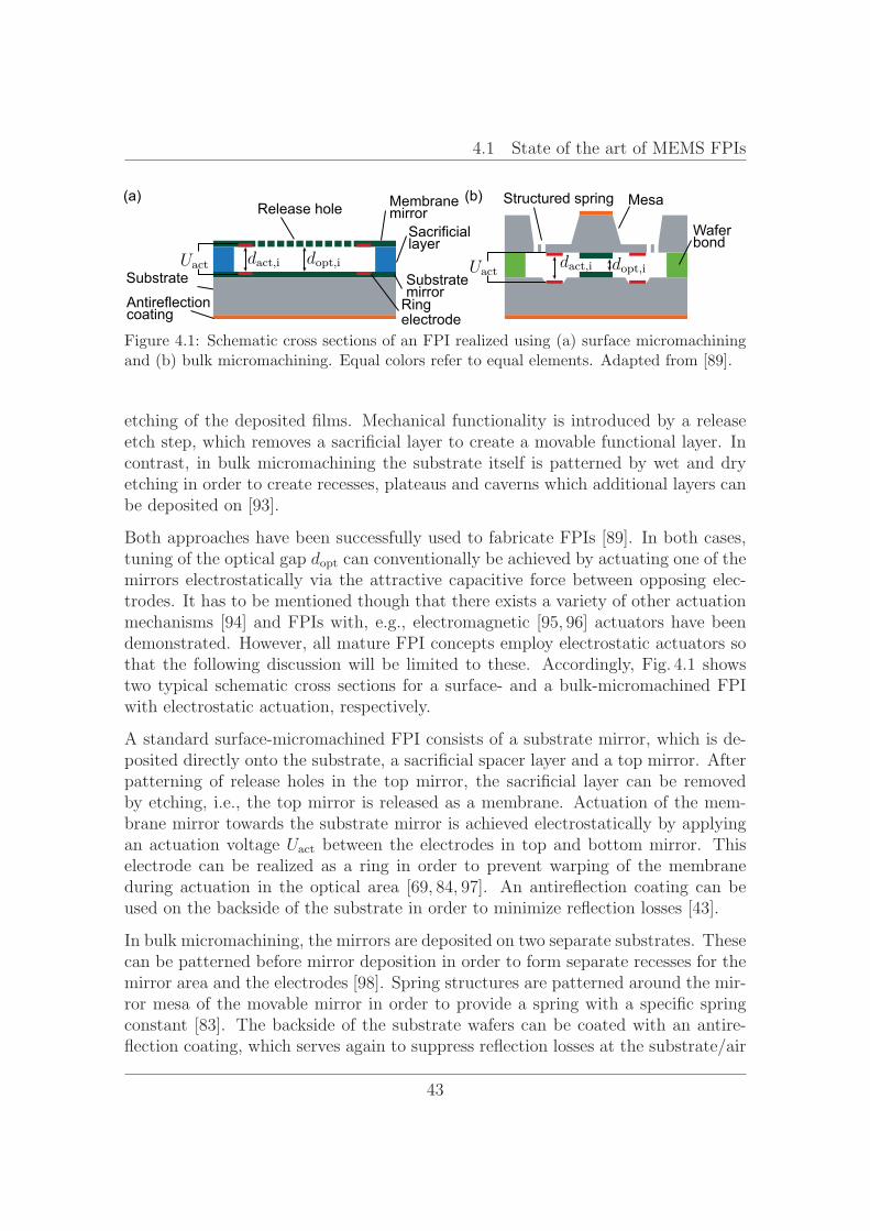
4.1 State of the art of MEMS FPIs
U d dU d d
Figure 4.1: Schematic cross sections of an FPI realized using (a) surface micromachiningand (b) bulk micromachining. Equal colors refer to equal elements. Adapted from [89].
etching of the deposited films. Mechanical functionality is introduced by a releaseetch step, which removes a sacrificial layer to create a movable functional layer. Incontrast, in bulk micromachining the substrate itself is patterned by wet and dryetching in order to create recesses, plateaus and caverns which additional layers canbe deposited on [93].
Both approaches have been successfully used to fabricate FPIs [89]. In both cases,tuning of the optical gap d can conventionally be achieved by actuating one of themirrors electrostatically via the attractive capacitive force between opposing elec-trodes. It has to be mentioned though that there exists a variety of other actuationmechanisms [94] and FPIs with, e.g., electromagnetic [95, 96] actuators have beendemonstrated. However, all mature FPI concepts employ electrostatic actuators sothat the following discussion will be limited to these. Accordingly, Fig. 4.1 showstwo typical schematic cross sections for a surface- and a bulk-micromachined FPIwith electrostatic actuation, respectively.
A standard surface-micromachined FPI consists of a substrate mirror, which is de-posited directly onto the substrate, a sacrificial spacer layer and a top mirror. Afterpatterning of release holes in the top mirror, the sacrificial layer can be removedby etching, i.e., the top mirror is released as a membrane. Actuation of the mem-brane mirror towards the substrate mirror is achieved electrostatically by applyingan actuation voltage U between the electrodes in top and bottom mirror. Thiselectrode can be realized as a ring in order to prevent warping of the membraneduring actuation in the optical area [69, 84, 97]. An antireflection coating can beused on the backside of the substrate in order to minimize reflection losses [43].
In bulk micromachining, the mirrors are deposited on two separate substrates. Thesecan be patterned before mirror deposition in order to form separate recesses for themirror area and the electrodes [98]. Spring structures are patterned around the mir-ror mesa of the movable mirror in order to provide a spring with a specific springconstant [83]. The backside of the substrate wafers can be coated with an antire-flection coating, which serves again to suppress reflection losses at the substrate/air
43
Chapter 4. Broadband NIR MEMS FPIs: Opportunities and challenges
interface [83]. As a final step, the substrate wafers are bonded together in order toform the cavity [83,98]. During actuation, the movable upper mirror is electrostati-cally pulled towards the lower mirror.
The last chapter has shown that an FPI with broad SWR requires two parallelmirrors, i.e., free of significant warp, tilt and roughness. In first order operationthey need to be separated by an optical gap d of roughly half the transmittancewavelength and this gap needs to be changed by roughly a factor of two by theactuator. The following discussion about the differences between bulk- and surface-micromachined FPIs with respect to these factors shall clarify the functional rela-tionships in order to motivate the later choice for a surface-micromachined approach.A more detailed treatment will follow during the actual MEMS design in chapter 6.
Mirror flatnessBulk: The movable mirror is depositedon a thick mesa structure which will bedeformed by any residual stress in themirror layers. The mirror should there-fore be free of mechanical stress.
Surface: In order to prevent the re-leased membrane mirror from buckling,it needs to be in a state of slight tensilestress.
Tilt and initial optical gap d ,
Bulk: The initial optical gap d , is de-termined by the thickness of the bond-material or, in case of direct wafer bond-ing, by the depth of the mirror plateaus.Precise uniformity and thickness controlof the bondmaterial is required for paral-lel alignment at a fixed d , . For a largecoefficient of thermal expansion (CTE)of the bondmaterial, d , may shift withtemperature [77].
Surface: The initial optical gap d , isdetermined by the thickness of the sac-rificial layer. Homogeneous depositionwith a well-known rate is necessary forachieving parallel mirrors at a desiredseparation. Achievable sacrificial layerthicknesses may impose an upper limiton the initial separation and thereforethe initial optical gap d , .
Mirror roughnessBulk: Both mirrors can be deposited di-rectly onto clean substrates of opticalquality by a variety of deposition meth-ods so that low roughness can easily beachieved.
Surface: The membrane mirror is de-posited on top of the sacrificial layer sothat roughness can accumulate duringdeposition. It is exposed to the etchmedium during the release process whichcan introduce further roughness.
For electrostatic actuation, displacement Δd at a given voltage results from aforce equilibrium between an attractive capacitive force and a restoring spring force(see Appendix D for a detailed introduction). It should be noted at this pointthat without a further mechanical transmission element such as a lever, actuator
44
4.1 State of the art of MEMS FPIs
displacement Δd equals the change in the optical gap Δd in magnitude. Theactuation capacitance is determined by the electrode area A and their initialseparation Δd , (called initial actuation gap in the following) while the springforce depends on the spring constant k.
Initial actuation gap Δd ,
Bulk: 3D structuring of the substrateallows the actuation electrodes to beplaced on a plateau or recess with re-spect to the mirrors. Thereby, the initialactuation gap Δd , can independentlybe chosen larger or smaller than the ini-tial optical gap Δd , [99].
Surface: Since the mirror membranesneed to be free of topography, elec-trodes can only usefully be implementedin the same plane as the mirrors. There-fore, initial optical and actuation gap areequal.
Electrode area ABulk: Electrode area can be chosen in-dependently of the mirror area. Size de-pends on the allowed range of actuationvoltages U .
Surface: Electrode can be integratedinto the mirror. However, the mem-brane bends during actuation in the elec-trode region reducing mirror parallelism(see section 6.2). Active electrode areashould therefore lie outside the activeoptical area.
Spring constant kBulk: Spring constant k can be designedby patterning dedicated springs into theupper substrate.
Surface: The deflected membrane causesthe restoring force. Spring constantk depends on the residual mechanicalstress σ in the membrane and its thick-ness d .
One point that has been excluded in the discussion so far is the fundamental reso-nance frequency f ,(m,n) which depends on the spring constant k and inversely onits mass. Consequently, bulk-micromachined FPIs have a lower resonance frequencythan their surface-micromachined counterpart due to the large mass of the mirrormesa. Therefore, they are prone to coupling of external vibrations [100] and theinitial optical gap may be sensitive to gravitation [101].
From the discussion above, it can be concluded that a bulk-micromachined FPIpossesses more degrees of freedom regarding its design since many of the afore-mentioned design parameters are decoupled, i.e., they can be chosen independently.For a surface-micromachined FPI on the other hand, the released membrane has tofunction as a mirror, spring and electrode simultaneously, which usually leads to aperformance trade-off.
45
Chapter 4. Broadband NIR MEMS FPIs: Opportunities and challenges
However, due to the single wafer process and potentially smaller chip dimensions,surface-micromachined FPIs promise lower fabrication cost per unit and a higherdegree of miniaturization. It will be one of the main tasks of this thesis to findsolutions which enable low-cost surface-micromachined FPIs with more degrees offreedom for the design in order to circumvent these performance trade-offs.
4.1.2 Comparison of mirror concepts
DBRs as introduced in subsection 3.3.1 are the dominant mirror design found instate-of-the-art FPIs. However, a few other mirror concepts have been demonstratedin MEMS FPIs which shall briefly be introduced in this subsection.
The popularity of DBRs is related to the following aspects: The refractive indexcontrast between available MEMS materials1 is considerably larger than, e.g., invertical-cavity surface-emitting lasers, so that only few layers (usually between threeand seven) are needed to achieve the desired reflectance. If the materials are trans-parent in the spectral region of interest, the mirrors are free of absorption. Further-more, the mirrors can be fabricated without using metals which can be an importantaspect if CMOS-compatibility is a process requirement.
There are, however, designs relying explicitly on metal reflectors which can providebroadband reflectance [102, 103]. In these cases, silver is used as it allows for thehighest reflectance above 500 nm [76] and doesn’t absorb as strongly as other metals.Still, silver thickness cannot exceed a few tens of nanometers because absorption be-comes too large otherwise. Therefore, such thin silver layers have to be mechanicallystabilized and protected from corrosion in atmosphere. This has for example beendone using aluminum oxide deposited by atomic layer deposition (ALD) [103].
Another recent development are mirrors based on a metallic subwavelength grating(SWG), i.e., a reflector which is structured by in-plane subwavelength features inorder to create a 2D photonic crystal. This leads to resonance phenomena whichresult in high reflectance. As an example, structured aluminum pads on asupport membrane have been demonstrated [104]. They show considerably lowerreflectance than a DBR. However, they reflect over a broader spectral range andshow less phase shift upon reflection. Alternatively, purely dielectric photonic crystalreflectors have been shown with high reflectance but very limited bandwidth of onlyfew tens of nanometers in the visible [105]. A similar filter has been built in the MIRusing a structured silicon membrane [106]. From a fabrication point of view, suchreflectors require advanced lithography techniques which are not always available ina MEMS production environment.
1more on this in subsection 4.2.1
46
4.1 State of the art of MEMS FPIs
4.1.3 Overview of published designs
After the general characteristics of surface- and bulk-micromachined FPIs and therespective mirror technologies have been introduced, some of the actual solutions interms of published devices will be presented in this subsection. Besides an overviewof the state of the art, performance indicators for these devices will explicitly bestated as a benchmark for the improvements proposed in this thesis.
For the sake of brevity, the discussion will be limited to groups which, to the author’sknowledge, are active until today. For a more complete review that also covers earlierwork the reader may be referred to the article written by Ebermann et al. [89].
Table 4.1 presents a list of published devices ordered by their micromachiningapproach, group and mirror technology. The reported SWR and the maximumachieved FWHM within this SWR are given as performance indicators. Addition-ally, the working interference order is included. For a better visualization, the SWRis furthermore plotted in Fig. 4.2. Two different wavelength scales have been chosenfor the VIS-NIR and the MIR-TIR spectral range for better readability.
The VTT Technical Research Centre of Finland is among the first groups whichworked on MEMS FPIs starting in the late 90s [5, 110]. They have also pioneeredring electrodes for electrostatic actuation [69,110] and their FPI designs correspondclosely to the schematic shown in Fig 4.1 (a). Until today, they have shown a broadrange of surface micromachined devices using different materials and depositionprocesses for their Bragg mirrors. In the visible ALD / DBRs [42,107] aswell as capped silver [103] has been used. It is noteworthy that they proposedto use several interference orders matched to the three channels of an RGB imagesensor in order to build a low-cost HSI device in the visible [103].
For the NIR around and below they showed second order FPIs with five layerDBRs made from poly-Si and silicon-rich nitride (SiRiN) deposited by low-pressurechemical vapor deposition (LPCVD) [43]. These have been commercialized by aspin-off called Spectral Engines Oy as three full miniaturized spectrometry systems,each with a slightly shifted SWR, including Bluetooth and cloud connectivity [11,92].
Their last mirror technology consists of three layer LPCVD poly-Si/air reflectorswhere the two silicon layers are periodically connected by anchor structures [91] andthe air layer results from sacrificial etching of a SiO2 layer. The mirrors have initiallybeen developed for the TIR [84, 91] but have recently been shown to be functionalwith smaller thicknesses as well down to wavelengths of . [58]. Apart from theALD / FPIs, all devices use silicon oxide (either PECVD or LPCVD) asthe sacrificial layer. The former uses a sacrificial photoresist instead [42].
47
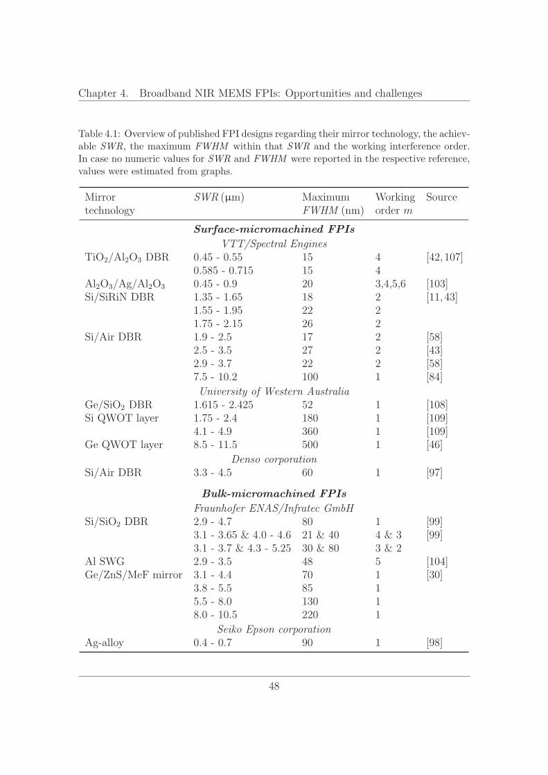
Chapter 4. Broadband NIR MEMS FPIs: Opportunities and challenges
Table 4.1: Overview of published FPI designs regarding their mirror technology, the achiev-able SWR, the maximum FWHM within that SWR and the working interference order.In case no numeric values for SWR and FWHM were reported in the respective reference,values were estimated from graphs.
Mirrortechnology
SWR (μm) MaximumFWHM (nm)
Workingorder m
Source
Surface-micromachined FPIs
VTT/Spectral EnginesTiO2/Al2O3 DBR 0.45 - 0.55 15 4 [42,107]
0.585 - 0.715 15 4Al2O3/Ag/Al2O3 0.45 - 0.9 20 3,4,5,6 [103]Si/SiRiN DBR 1.35 - 1.65 18 2 [11,43]
1.55 - 1.95 22 21.75 - 2.15 26 2
Si/Air DBR 1.9 - 2.5 17 2 [58]2.5 - 3.5 27 2 [43]2.9 - 3.7 22 2 [58]7.5 - 10.2 100 1 [84]
University of Western AustraliaGe/SiO2 DBR 1.615 - 2.425 52 1 [108]Si QWOT layer 1.75 - 2.4 180 1 [109]
4.1 - 4.9 360 1 [109]Ge QWOT layer 8.5 - 11.5 500 1 [46]
Denso corporationSi/Air DBR 3.3 - 4.5 60 1 [97]
Bulk-micromachined FPIs
Fraunhofer ENAS/Infratec GmbHSi/SiO2 DBR 2.9 - 4.7 80 1 [99]
3.1 - 3.65 & 4.0 - 4.6 21 & 40 4 & 3 [99]3.1 - 3.7 & 4.3 - 5.25 30 & 80 3 & 2
Al SWG 2.9 - 3.5 48 5 [104]Ge/ZnS/MeF mirror 3.1 - 4.4 70 1 [30]
3.8 - 5.5 85 15.5 - 8.0 130 18.0 - 10.5 220 1
Seiko Epson corporationAg-alloy 0.4 - 0.7 90 1 [98]
48
4.1 State of the art of MEMS FPIs
The microelectronics research group at the University of Western Australia pursuesa surface micromachining approach with polyimide as the sacrificial material wherethe filter can directly be integrated on a HgCdTe detector [111]. Deposition processesare therefore restricted to a low-temperature regime [45]. Their initial design differsfrom the general schematic in Fig. 4.1 (a) in the sense that the membrane mirroris supported by a low-stress PECVD silicon nitride layer with structured flexureswhich are connected to the substrate in four corners [45, 108]. While this designdecouples the optical mirror from the mechanical actuator properties to some extent,it is very sensitive to residual stress as well as stress gradients even at small mirrordiameters in the range of [108, 112]. They also presented a modified designwith two-sided clamped beam actuators, which was able to extend the travel rangebeyond the classical pull-in limit [108]. Details will be discussed further below insubsection 4.2.2.
Regarding their mirrors, they employ DBRs made from Ge/ for the NIR abovethe Ge absorption edge [112] and Ge/ZnS for the TIR [113]. They also proposedto use single QWOT layers of either Si or Ge for multispectral imaging applicationswhich require a lower number of spectral bands to be resolved compared to HSI [46].Furthermore, Si/air DBRs have recently been built for the NIR [114, 115] but notunable FPIs have been presented yet.
A surface-micromachined FPI with a three layer Si/air DBR similar to the VTTapproach shown in Fig. 4.1 (a) has been presented by the Denso Corporation for theMIR [97]. The mirror differs from the VTT design in the sense that the mirror Silayers are stabilized by an interconnected honeycomb structure instead of isolatedanchors. A ring electrode is employed for actuation.
Fraunhofer ENAS, TU Chemnitz and Infratec GmbH have started working on bulk-micromachined FPIs in 2001 with their designs close to the schematic shown inFig. 4.1 (b) [89]. Their focus lies in the MIR for gas sensing of hydrocarbonspecies [116]. Filters with detector are available in a TO package. Initially, LPCVDpoly-Si/SiO2 DBRs were used [99, 117]. Later, the spectral range was extendedtowards longer wavelengths where SiO2 is absorbing. Therefore, thin-film mirrorswith three materials, Ge, ZnS and a metal fluoride (MeF) deposited by ion-assistedsputtering were used. Additionally, three materials give more degrees of freedom forsimultaneously optimizing reflectance and residual stress [30,83].
A special concept is their so-called dual-band reflector with high reflectance in twoseparate spectral ranges. When these reflectance bands are matched with two inter-ference orders, the SWR can be increased [77,99]. Separation of the two transmittedsignals is achieved by using a dicroic mirror which directs the 3rd and 4th ordertransmission onto different detectors.
49
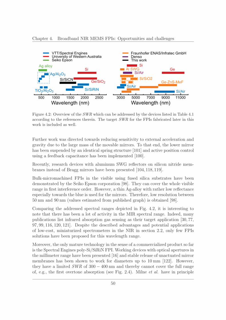
Chapter 4. Broadband NIR MEMS FPIs: Opportunities and challenges
University of Western AustraliaVTT/Spectral Engines
Seiko Epson This work
Fraunhofer ENAS/Infratec GmbHDenso
500 1000 1500 2000 2500Wavelength (nm)
Si/SiRiNTiO2/Al2O3
Si/SiCN Ge/SiO2
SiAg/Al2O3
Ag alloy
Wavelength (nm)
GeSi
Si/Air
Al SWGSi/Air
Si/Air
Ge-ZnS-MeFSi/SiO2
3000 5000 7000 9000 11000
Figure 4.2: Overview of the SWR which can be addressed by the devices listed in Table 4.1according to the references therein. The target SWR for the FPIs fabricated later in thiswork is included as well.
Further work was directed towards reducing sensitivity to external acceleration andgravity due to the large mass of the movable mirrors. To that end, the lower mirrorhas been suspended by an identical spring structure [101] and active position controlusing a feedback capacitance has been implemented [100].
Recently, research devices with aluminum SWG reflectors on silicon nitride mem-branes instead of Bragg mirrors have been presented [104,118,119].
Bulk-micromachined FPIs in the visible using fused silica substrates have beendemonstrated by the Seiko Epson corporation [98]. They can cover the whole visiblerange in first interference order. However, a thin Ag-alloy with rather low reflectanceespecially towards the blue is used for the mirrors. Therefore, low resolution between
and (values estimated from published graph) is obtained [98].
Comparing the addressed spectral ranges depicted in Fig. 4.2, it is interesting tonote that there has been a lot of activity in the MIR spectral range. Indeed, manypublications list infrared absorption gas sensing as their target application [30, 77,97, 99, 116, 120, 121]. Despite the described advantages and potential applicationsof low-cost, miniaturized spectrometers in the NIR in section 2.2, only few FPIssolutions have been proposed for this wavelength range.
Moreover, the only mature technology in the sense of a commercialized product so faris the Spectral Engines poly-Si/SiRiN FPI. Working devices with optical apertures inthe millimeter range have been presented [16] and stable release of unactuated mirrormembranes has been shown to work for diameters up to [122]. However,they have a limited SWR of − and thereby cannot cover the full rangeof, e.g., the first overtone absorption (see Fig. 2.4). Milne et al. have in principle
50
4.2 Limitations of surface-micromachined FPIs
demonstrated a larger SWR but their working devices had an aperture ofdiameter so that the achievable throughput is limited [108].
Accordingly, surface-micromachined FPIs combining a large SWR and a large mil-limeter-sized aperture remain an open research topic which will be addressed inthis thesis. To that end, the reasons for the aforementioned limitations regardingSWR and aperture size are analyzed in the next section so that specific solutionapproaches can be derived afterwards.
4.2 Limitations of surface-micromachined FPIs
The previous sections have illustrated that there exists a large solution space forpossible FPI devices. The decision for a specific design will always be affected bymany factors such as the required SWR, resolution, throughput, robustness againstvibrations and cost to name just a few which in turn depend on the target applica-tion. As mentioned before, this thesis aims specifically at a low-cost FPI with bothan increased SWR in the NIR as well as larger membrane diameters compared tostate-of-the-art FPIs.
In subsection 4.1.1, it has been noted that a surface-micromachined FPI can ulti-mately be fabricated at smaller size and lower cost compared to bulk-micromachinedFPIs. However, since the mirror membrane has to act as a mirror, spring and elec-trode simultaneously, there is a large number of constraints to be met for the mirrormaterials. Additional boundary conditions arise from the fabrication process whichrequires the mirror to be stable towards the sacrificial layer etchant and limits thepossible topography. Consequently, a trade-off between different performance crite-ria must be found.
In this section, three major shortcomings of state-of-the-art surface-micromachinedFPIs will be identified and it will be shown why they fundamentally limit the achiev-able SWR or optical aperture size. From the previous paragraph, it can be de-duced that the materials chosen for the mirrors play a critical role in a surface-micromachined FPI. Therefore, the available MEMS mirror materials are reviewedin subsection 4.2.1 and material property requirements for an optimal low-refractiveindex material in a DBR are formulated.
Subsequently, limitations for the achievable mirror travel range stemming from thepull-in phenomenon of electrostatic actuation will be addressed in subsection 4.2.2.
Last, sources for optical gap inhomogeneity which deteriorate filter resolution andtheir relationship to the aperture area will be discussed in subsection 4.2.3.
51
Chapter 4. Broadband NIR MEMS FPIs: Opportunities and challenges
4.2.1 Influence of the low-refractive index material in theBragg reflector
As described above, the mirror materials for a DBR affect the FPI from an optical(reflectance), mechanical (spring) and electrical (actuation electrode) point of view.According to section 3.4, the SWR can be limited optically either by the width of thehigh reflectance zone Δλ or the FSR of the first interference order. Both of thesedepend on the refractive index contrast Δn of the chosen materials. Additionally,the mirror needs to be flat after the release and act as a spring with defined springconstant under actuation. These mechanical properties are mainly governed by theresidual mechanical stress σ, which needs to be slightly tensile for achieving a flatreleased membrane mirror. Obviously, the mirror materials also need to be resistanttowards the sacrificial layer etchant. Since is the de facto standard sacrificialmaterial in MEMS it will be also used for sacrificial layers in this thesis so that vaporHF resistance of the mirrors is a key requirement.
The dominant materials in classical MEMS are those known from microelectronics,i.e., silicon, silicon dioxide and silicon nitride [93]. They form a versatile toolset forengineering microelectromechanical systems since they are complementary metal ox-ide semiconductor (CMOS)-compatible and allow for precise tuning of a device’s me-chanical properties via structuring and electrical properties via doping/passivation.For optical applications, i.e., microoptoelectromechanical systems, refractive indexand transparency have to be considered as well. Table 4.2 lists the relevant proper-ties of these standard materials for usage in a membrane DBR in this thesis, namelyrefractive index, mechanical stress and vapor HF resistance.
For wavelengths above its absorption edge ( at room temperature for thecrystalline phase [55]), Si is a good candidate for the high refractive index material.It is a well known MEMS material compatible both with LPCVD and PECVD witha refractive index around 3.5 in the NIR. Furthermore, it exhibits excellent stabilityagainst HF etching, hence its usage as the functional mechanical material in moststandard MEMS. Last but not least, Si can be made conductive by doping so thatit can be used for the actuation electrodes as well.
Indeed, looking at Table 4.1, all published DBRs use either Si or Ge as the highrefractive index layer. Ge, though with an even higher refractive index (n > 4),absorbs above its band gap at E , = . ( ) [125]. Since this thesisexplicitly wants to address the spectral range below , Si remains as thenatural choice for the high refractive index material.
The situation is more complicated for the low-refractive index material. According
52
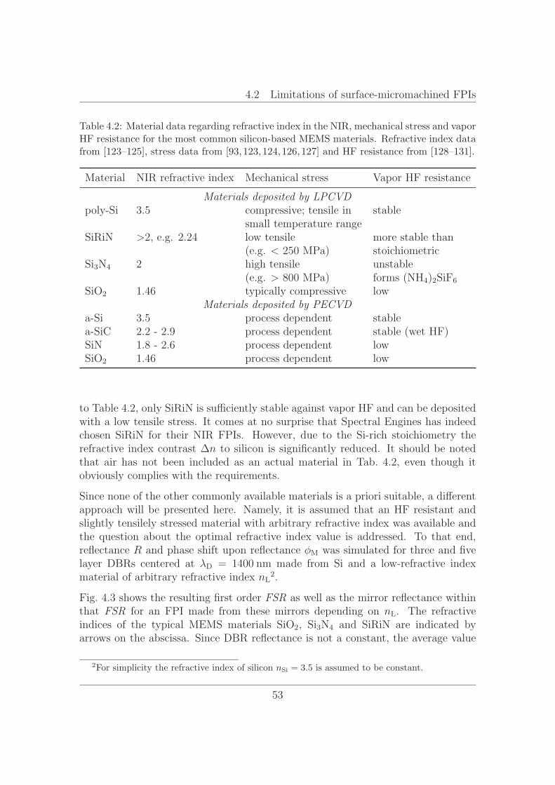
4.2 Limitations of surface-micromachined FPIs
Table 4.2: Material data regarding refractive index in the NIR, mechanical stress and vaporHF resistance for the most common silicon-based MEMS materials. Refractive index datafrom [123–125], stress data from [93,123,124,126,127] and HF resistance from [128–131].
Material NIR refractive index Mechanical stress Vapor HF resistance
Materials deposited by LPCVDpoly-Si 3.5 compressive; tensile in
small temperature rangestable
SiRiN >2, e.g. 2.24 low tensile(e.g. < 250 MPa)
more stable thanstoichiometric
Si3N4 2 high tensile(e.g. > 800 MPa)
unstableforms (NH4)2SiF6
SiO2 1.46 typically compressive lowMaterials deposited by PECVD
a-Si 3.5 process dependent stablea-SiC 2.2 - 2.9 process dependent stable (wet HF)SiN 1.8 - 2.6 process dependent lowSiO2 1.46 process dependent low
to Table 4.2, only SiRiN is sufficiently stable against vapor HF and can be depositedwith a low tensile stress. It comes at no surprise that Spectral Engines has indeedchosen SiRiN for their NIR FPIs. However, due to the Si-rich stoichiometry therefractive index contrast Δn to silicon is significantly reduced. It should be notedthat air has not been included as an actual material in Tab. 4.2, even though itobviously complies with the requirements.
Since none of the other commonly available materials is a priori suitable, a differentapproach will be presented here. Namely, it is assumed that an HF resistant andslightly tensilely stressed material with arbitrary refractive index was available andthe question about the optimal refractive index value is addressed. To that end,reflectance R and phase shift upon reflectance φ was simulated for three and fivelayer DBRs centered at λ = made from Si and a low-refractive indexmaterial of arbitrary refractive index n 2.
Fig. 4.3 shows the resulting first order FSR as well as the mirror reflectance withinthat FSR for an FPI made from these mirrors depending on n . The refractiveindices of the typical MEMS materials , and SiRiN are indicated byarrows on the abscissa. Since DBR reflectance is not a constant, the average value
2For simplicity the refractive index of silicon n = 3.5 is assumed to be constant.
53
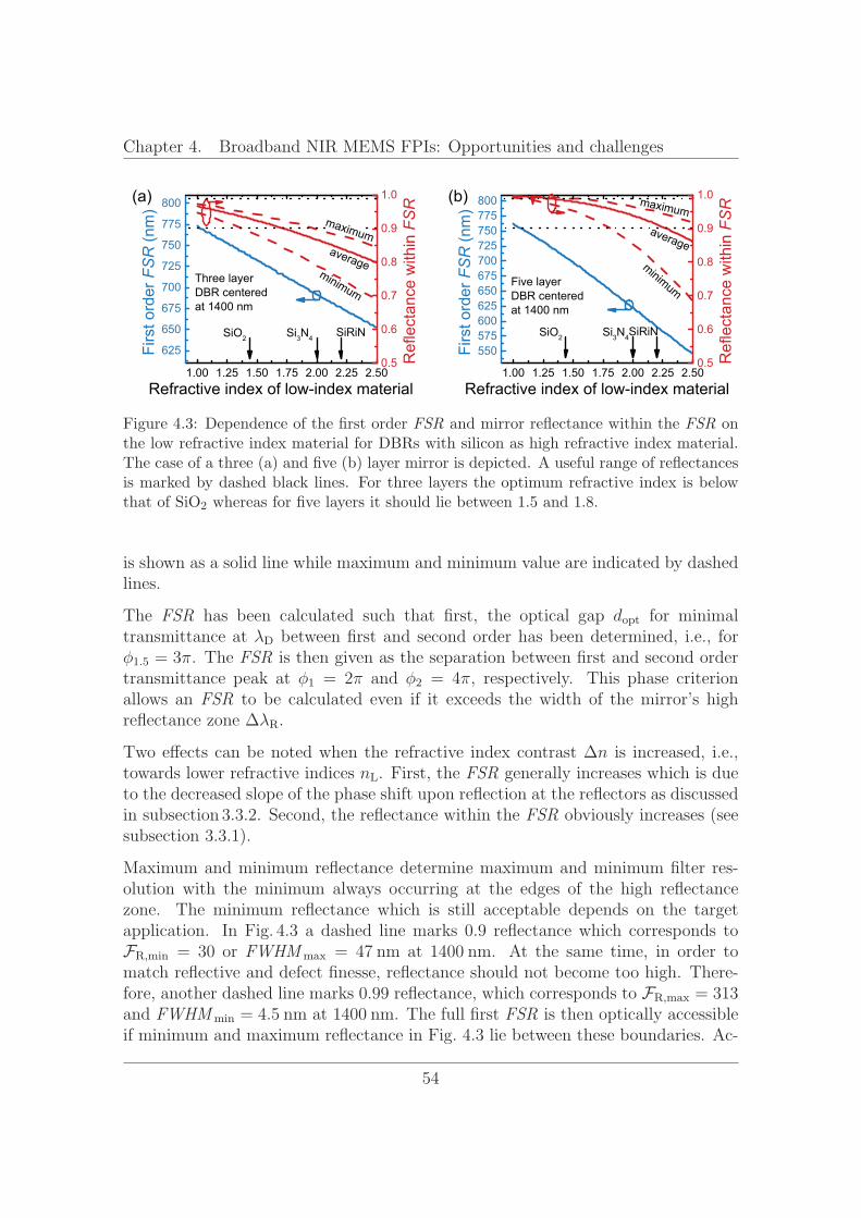
Chapter 4. Broadband NIR MEMS FPIs: Opportunities and challenges
1.00 1.25 1.50 1.75 2.00 2.25 2.50
625
650
675
700
725
750
775
800
Three layerDBR centeredat 1400 nm
SiRiNSi3N4SiO2
minimum
average
FirstorderFSR(nm)
Refractive index of low-index material
maximum
0.5
0.6
0.7
0.8
0.9
1.0
ReflectancewithinFSR(a)
1.00 1.25 1.50 1.75 2.00 2.25 2.50
550575600625650675700725750775800
FirstorderFSR(nm)
Refractive index of low-index material
Five layerDBR centeredat 1400 nm
minimum
average
maximum
SiO2 Si3N4SiRiN
0.5
0.6
0.7
0.8
0.9
1.0
ReflectancewithinFSR(b)
Figure 4.3: Dependence of the first order FSR and mirror reflectance within the FSR onthe low refractive index material for DBRs with silicon as high refractive index material.The case of a three (a) and five (b) layer mirror is depicted. A useful range of reflectancesis marked by dashed black lines. For three layers the optimum refractive index is belowthat of SiO2 whereas for five layers it should lie between 1.5 and 1.8.
is shown as a solid line while maximum and minimum value are indicated by dashedlines.
The FSR has been calculated such that first, the optical gap d for minimaltransmittance at λ between first and second order has been determined, i.e., forφ1.5 = 3π. The FSR is then given as the separation between first and second ordertransmittance peak at φ1 = 2π and φ2 = 4π, respectively. This phase criterionallows an FSR to be calculated even if it exceeds the width of the mirror’s highreflectance zone Δλ .
Two effects can be noted when the refractive index contrast Δn is increased, i.e.,towards lower refractive indices n . First, the FSR generally increases which is dueto the decreased slope of the phase shift upon reflection at the reflectors as discussedin subsection 3.3.2. Second, the reflectance within the FSR obviously increases (seesubsection 3.3.1).
Maximum and minimum reflectance determine maximum and minimum filter res-olution with the minimum always occurring at the edges of the high reflectancezone. The minimum reflectance which is still acceptable depends on the targetapplication. In Fig. 4.3 a dashed line marks 0.9 reflectance which corresponds toF , = 30 or FWHM = at . At the same time, in order tomatch reflective and defect finesse, reflectance should not become too high. There-fore, another dashed line marks 0.99 reflectance, which corresponds to F , = 313and FWHM = . at . The full first FSR is then optically accessibleif minimum and maximum reflectance in Fig. 4.3 lie between these boundaries. Ac-
54
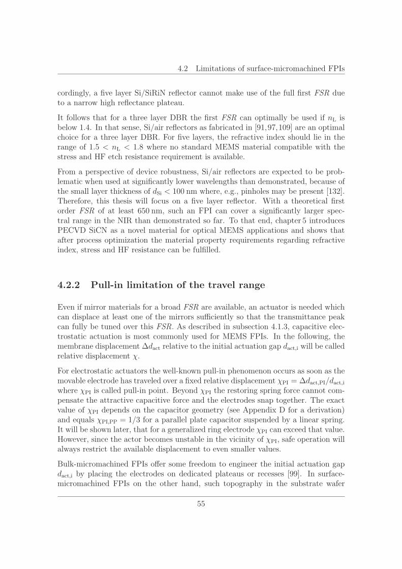
4.2 Limitations of surface-micromachined FPIs
cordingly, a five layer Si/SiRiN reflector cannot make use of the full first FSR dueto a narrow high reflectance plateau.
It follows that for a three layer DBR the first FSR can optimally be used if n isbelow 1.4. In that sense, Si/air reflectors as fabricated in [91,97,109] are an optimalchoice for a three layer DBR. For five layers, the refractive index should lie in therange of 1.5 < n < 1.8 where no standard MEMS material compatible with thestress and HF etch resistance requirement is available.
From a perspective of device robustness, Si/air reflectors are expected to be prob-lematic when used at significantly lower wavelengths than demonstrated, because ofthe small layer thickness of d < where, e.g., pinholes may be present [132].Therefore, this thesis will focus on a five layer reflector. With a theoretical firstorder FSR of at least , such an FPI can cover a significantly larger spec-tral range in the NIR than demonstrated so far. To that end, chapter 5 introducesPECVD SiCN as a novel material for optical MEMS applications and shows thatafter process optimization the material property requirements regarding refractiveindex, stress and HF resistance can be fulfilled.
4.2.2 Pull-in limitation of the travel range
Even if mirror materials for a broad FSR are available, an actuator is needed whichcan displace at least one of the mirrors sufficiently so that the transmittance peakcan fully be tuned over this FSR. As described in subsection 4.1.3, capacitive elec-trostatic actuation is most commonly used for MEMS FPIs. In the following, themembrane displacement Δd relative to the initial actuation gap d , will be calledrelative displacement χ.
For electrostatic actuators the well-known pull-in phenomenon occurs as soon as themovable electrode has traveled over a fixed relative displacement χ = Δd , /d ,
where χ is called pull-in point. Beyond χ the restoring spring force cannot com-pensate the attractive capacitive force and the electrodes snap together. The exactvalue of χ depends on the capacitor geometry (see Appendix D for a derivation)and equals χ , = 1/3 for a parallel plate capacitor suspended by a linear spring.It will be shown later, that for a generalized ring electrode χ can exceed that value.However, since the actor becomes unstable in the vicinity of χ , safe operation willalways restrict the available displacement to even smaller values.
Bulk-micromachined FPIs offer some freedom to engineer the initial actuation gapd , by placing the electrodes on dedicated plateaus or recesses [99]. In surface-micromachined FPIs on the other hand, such topography in the substrate wafer
55
Chapter 4. Broadband NIR MEMS FPIs: Opportunities and challenges
1 2 3
0.25
0.30
0.35
0.40
0.45
0.50
0.55
0.60
Rel
ativ
e tra
vel r
ange
Interference order
No phase-shiftupon reflection
Pull-in
Single membrane FPIwith full FSR actuation
Figure 4.4: Required relative optical travel range χ for full transmittance peak tuningover the 1st, 2nd or 3rd FSR for several choices of the low refractive index material. Forfull first order tuning a relative travel range of at least 0.5 is needed. This lies beyond thepull-in point χ , of parallel plate actuators.
cannot easily be created since it is conformally replicated in the following depositedlayers3. Therefore, the initial actuation gap d , essentially equals the initial opticalgap d , .
Fig. 4.4 shows the maximum relative travel range χ required for actuating suchan FPI with a five layer DBR made from a variety of low-refractive index materialsand silicon over a full FSR for different interference orders. A hypothetical mirrorwithout phase shift upon reflection φ is considered as well. The pull-in point forparallel plate capacitor actuation χ , is marked by a dashed line.
From the discussion in section 3.1.2, it can be deduced that the relative travel rangeχ for tuning the transmittance peak of the m-th interference order without phaseshift upon reflection φ is (m+1)−1. The required relative travel range χ becomeslarger, the larger the slope of the dispersion in φ , i.e., the lower the refractive indexcontrast Δn of the DBR materials (see subsection 3.3.2).
Consequently, first order FPIs require relative travel ranges χ > 0.5, thus farexceeding the pull-in point. Even in second order, displacement up to the pull-inpoint would be required which, as noted above, is outside a safe operation regime.
This limitation has been recognized before and several techniques for extending thetravel range have been proposed [14]. These include charge control instead of voltagecontrol and closed-loop feedback [14] which come at the expense of higher complexityin the drive electronics. It has been claimed that a second fixed capacitance in
3Topography can in principle be removed by polishing methods such as chemical-mechanicalpolishing. However, this would complicate an accurate prediction of the initial optical gap d , .
56
4.2 Limitations of surface-micromachined FPIs
series with the actuation capacitance can be used to increase the effective d ,
[132]. Parasitic capacitances from the design and deposition inhomogeneities whichare hard to control are the main culprit in this approach [133]. Additionally, asmentioned already in subsection 4.1.3 double-sided clamped beam actuators withan increased travel range have been fabricated [108]. Last, a design with cascadedsprings has been proposed [134].
However, the underlying root cause remains, namely that d , = d , in thesesurface-micromachined FPIs. In the next section, a double membrane device archi-tecture will be proposed by which significantly larger travel ranges can be realized.
4.2.3 Stress-induced substrate curvature
It is well known that residual mechanical stress σ in deposited thin-films can crit-ically affect the performance of optical filters [135, 136] and MOEMS [3] due tothe resulting device deformations. In particular, free-standing structures such assteerable micromirrors suffer from deformation due to mechanical relaxation of thestressed part. Therefore, considerable effort is put into either controlling stressduring deposition by appropriate deposition parameters or compensating stress bymodifying the design, e.g., additional stiffening layers in freestanding structures orbackside depositions for fixed coatings [135].
In surface-micromachined FPIs, challenges due to mechanical relaxation have beenfaced for the freestanding mirrors in the early devices of the University of WesternAustralia [108, 111]. Precise control of the deposition conditions, e.g., for theirPECVD SiNx [111] and amorphous silicon (a-Si) [137] or post-deposition plasmatreatment [108] were necessary to ensure flatness of the movable mirror.
A released circular mirror membrane which is clamped at every position along itscircumference (e.g. VTT/Spectral Engines and Denso) provides robustness againstvertical stress gradients because its boundary is essentially defined by the fixture.Flat membranes can then more conveniently be achieved for a broader range oftensile stress levels (ultimately limited by the tensile strength) instead of requiringa stress-free mirror. However, stress in the deposited layers results in deformation ofthe substrate and thus the substrate mirror. The resulting consequences for mirrorparallelism will be discussed in this subsection.
First, the underlying theory will be shortly reviewed. Under the approximation ofan infinitely extending thin film of thickness d on a circular thick substrate ofthickness d , i.e., d d with uniform film stress σ, the substrate will bend
57
Chapter 4. Broadband NIR MEMS FPIs: Opportunities and challenges
with a constant radius of curvature r . It is related to the stress in the thin film σby the so called Stoney equation [138,139]:
r =Y d2
6d (1− μ )σ=
ζ
(1− μ )σ(4.1)
where Y is the Young modulus of the substrate and μ its Poisson ratio. As anabbreviation, ζ = Y d2 /6d is introduced.
For multiple thin films deposited on the same substrate the stress thickness producthas to be replaced by a sum over all layers as d σ =
∑j d ,jσj [139]. Curvature
radius r is typically large compared to MEMS dimensions so that the local substrateprofile can be approximated by a Taylor expansion as
z(x) = x2/(2r ). (4.2)
Since for a real MEMS thin-films are usually structured and the substrate is notcircular after chip dicing, the assumption of a uniform stress level is not necessarilyvalid. Therefore, as a more general case, an anisotropic in-plane stress of the formσx,y = σ ±Δσ, with average stress σ and biaxial mismatch Δσ will be considered.In that case, the radii of curvature differ for the x− and y− direction and are givenby [139]
r x, y =ζ
σx,y − μ σy,x. (4.3)
The surface profile of the substrate can then be written as a linear superposition:
z(x, y) =x2
2r x
+y2
2r y
=σ(1− μ )
2ζ
(x2 + y2
)+
Δσ(1 + μ )
2ζ
(x2 − y2
)=σ(1− μ )
2ζr2 +
Δσ(1 + μ )
2ζr2 2ϕ
= z(r) + Δz(r, ϕ)
(4.4)
where r and ϕ denote polar coordinates. Eq. 4.4 can now be used to study thesurface profile of both the substrate and the released membrane in a circular opticalaperture area.
Fig. 4.5 (lower surface) shows a plot of Eq. 4.4 for such a circular region of thesubstrate with radius r . A realistic order of magnitude regarding the samplesfabricated later in this thesis (r = . , d = , d = , σ =
,Δσ = , crystalline Si substrate) has been used for the parameters.
58
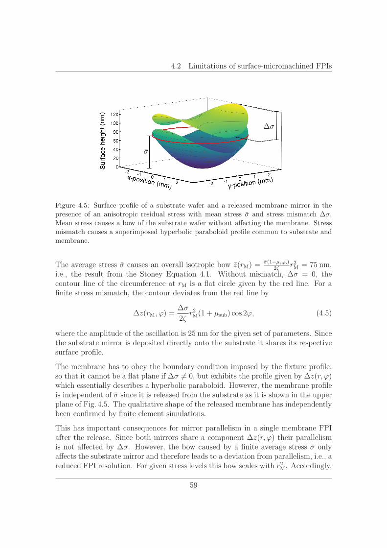
4.2 Limitations of surface-micromachined FPIs
σ
Δσ
Figure 4.5: Surface profile of a substrate wafer and a released membrane mirror in thepresence of an anisotropic residual stress with mean stress σ and stress mismatch Δσ.Mean stress causes a bow of the substrate wafer without affecting the membrane. Stressmismatch causes a superimposed hyperbolic paraboloid profile common to substrate andmembrane.
The average stress σ causes an overall isotropic bow z(r ) = σ(1−μ )2ζ
r2 = ,i.e., the result from the Stoney Equation 4.1. Without mismatch, Δσ = 0, thecontour line of the circumference at r is a flat circle given by the red line. For afinite stress mismatch, the contour deviates from the red line by
Δz(r , ϕ) =Δσ
2ζr2 (1 + μ ) 2ϕ, (4.5)
where the amplitude of the oscillation is for the given set of parameters. Sincethe substrate mirror is deposited directly onto the substrate it shares its respectivesurface profile.
The membrane has to obey the boundary condition imposed by the fixture profile,so that it cannot be a flat plane if Δσ �= 0, but exhibits the profile given by Δz(r, ϕ)which essentially describes a hyperbolic paraboloid. However, the membrane profileis independent of σ since it is released from the substrate as it is shown in the upperplane of Fig. 4.5. The qualitative shape of the released membrane has independentlybeen confirmed by finite element simulations.
This has important consequences for mirror parallelism in a single membrane FPIafter the release. Since both mirrors share a component Δz(r, ϕ) their parallelismis not affected by Δσ. However, the bow caused by a finite average stress σ onlyaffects the substrate mirror and therefore leads to a deviation from parallelism, i.e., areduced FPI resolution. For given stress levels this bow scales with r2 . Accordingly,
59
Chapter 4. Broadband NIR MEMS FPIs: Opportunities and challenges
for FPIs with high optical throughput requiring large apertures, a trade-off betweenthroughput and resolution will inevitably occur.
There are in principle two possibilities to reduce substrate bow z(r ). First, athicker substrate obviously helps because z(r ) ∝ d−2 . Alternatively, backsidestress compensation layers can be introduced. For an FPI fabricated by LPCVDdepositions, the double sided nature of the deposition automatically provides suchstress compensation. However, since the mirrors have to be removed on the backsidewithin the optical area, stress compensation cannot be complete.
Furthermore, the statement of mirror parallelism being deteriorated by an averagestress level σ while being independent of stress mismatch Δσ is more general inthe sense that it doesn’t only apply to residual thin-film stress. As an example,packaging can cause thermo-mechanical stress on the chip when chip and packagediffer in their CTE [5]. In that sense, an FPI architecture where such detrimentalstress influence is reduced by design would be highly beneficial.
4.3 Proposition: Double membrane FPIs for
increased spectral working ranges and
large diameters
The discussion in the previous section has shown that SWR, optical throughputand resolution in a surface-micromachined FPI can benefit from further develop-ments regarding both, the low-refractive index material and the device architecture.Specifically, an HF-resistant, slightly tensile material with a refractive index in therange of 1.5 < n < 1.8, which is not available among standard MEMS materials,has been identified as an optimum choice for a five layer DBR. Additionally, travelrange limitations in first order operation due to pull-in stemming from the coinci-dence of initial optical and actuation gap in current designs have been elucidated.Last, FPIs with large membrane diameters have been shown to be sensitive towardssubstrate wafer bow due to residual stress.
The surface-micromachined double membrane FPI proposed in this section is de-signed to enable full FSR tuning as well as highly parallel mirrors even at largemembrane diameters4. A cross section through such a device is shown in Fig. 4.6.
4The author acknowledges collaboration with his colleagues which resulted in the double mem-brane FPI structure. Most notably, Dr. Christoph Schelling, Dr. Reinhold Rodel, Dr. ChristophKrammer and Dr. Benedikt Stein from the Robert Bosch GmbH have contributed.
60
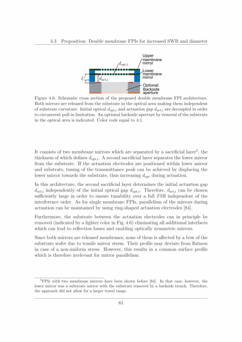
4.3 Proposition: Double membrane FPIs for increased SWR and diameter
U d
d
Figure 4.6: Schematic cross section of the proposed double membrane FPI architecture.Both mirrors are released from the substrate in the optical area making them independentof substrate curvature. Initial optical d , and actuation gap d , are decoupled in orderto circumvent pull-in limitation. An optional backside aperture by removal of the substratein the optical area is indicated. Color code equal to 4.1.
It consists of two membrane mirrors which are separated by a sacrificial layer5, thethickness of which defines d , . A second sacrificial layer separates the lower mirrorfrom the substrate. If the actuation electrodes are positioned within lower mirrorand substrate, tuning of the transmittance peak can be achieved by displacing thelower mirror towards the substrate, thus increasing d during actuation.
In this architecture, the second sacrificial layer determines the initial actuation gapd , independently of the initial optical gap d , . Therefore, d , can be chosensufficiently large in order to ensure tunability over a full FSR independent of theinterference order. As for single membrane FPIs, parallelism of the mirrors duringactuation can be maintained by using ring-shaped actuation electrodes [84].
Furthermore, the substrate between the actuation electrodes can in principle beremoved (indicated by a lighter color in Fig. 4.6) eliminating all additional interfaceswhich can lead to reflection losses and enabling optically symmetric mirrors.
Since both mirrors are released membranes, none of them is affected by a bow of thesubstrate wafer due to tensile mirror stress. Their profile may deviate from flatnessin case of a non-uniform stress. However, this results in a common surface profilewhich is therefore irrelevant for mirror parallelism.
5FPIs with two membrane mirrors have been shown before [84]. In that case, however, thelower mirror was a substrate mirror with the substrate removed by a backside trench. Therefore,the approach did not allow for a larger travel range.
61

Chapter 4. Broadband NIR MEMS FPIs: Opportunities and challenges
During the rest of this thesis, it will be shown that
• PECVD silicon carbonitride (SiCN) can be used as an HF-resistant, tensileand low-refractive index MEMS material [21, 22].
• double membrane FPIs can be fabricated with highly parallel mirrors even formembrane diameters up to [18].
• the first order transmittance peak of a double membrane FPI can be tunedover the full first FSR without pull-in [23].
As a first step, process conditions which lead to deposition of SiCN layers with theabove-mentioned properties will be explored in the next chapter.
62
Chapter 5
Amorphous hydrogenated siliconcarbonitride for MEMSapplications
The previous chapter has shown that there is a lack of MEMS materials which exhibita low refractive index while simultaneously being tensilely stressed and resistanttowards vapor HF etching. Not only the presented application in a MEMS FPIwould benefit from such a material, but optical MEMS in general which require abroader range of available refractive indices to tailor their device properties. Anexample would be a single layer antireflection coating (ARC) for a Si/air interfacewhich needs a refractive index of
√n ≈ 1.87 and by definition cannot be protected
by silicon during HF etching.
In order to ensure compatibility with existing equipment, chemical deposition fromthe vapor phase either by LPCVD or PECVD is beneficial. LPCVD commonly pro-duces high-quality, pinhole-free thin-films and can be used for batch processing [123].PECVD on the other hand offers more degrees of freedom because of the additionaldeposition parameters such as plasma power, plasma frequency or even frequencymixing [123]. Furthermore, as will be shown below, a lower deposition temperatureϑ compared to LPCVD allows for depositing material with a significant amountof incorporated hydrogen. While this is often an unwanted feature, it opens thepossibility to tune the refractive index and mechanical stress over a broad range ofvalues.
It is well known that smooth tailoring of material properties can be achieved bystoichiometry engineering in mixture materials [140, 141]. Following this idea, this
63
Chapter 5. Amorphous hydrogenated silicon carbonitride for MEMS applications
chapter introduces amorphous hydrogenated silicon carbonitride (SiCN)1 depositedby PECVD. When properly deposited, it retains high chemical inertness known fromamorphous SiC [130] but exhibits a reduced refractive index due to the admixtureof nitrogen and a lower density because of a residual hydrogen content.
The chapter starts with a short review of possible applications and deposition tech-niques for SiCN in section 5.1. Section 5.2 is then devoted to a detailed study of theeffects of deposition temperature ϑ not only on the material properties relevantfor application in a MEMS FPI but also on the underlying mechanisms regardingthe bonding structure. In section 5.3, it will be demonstrated that post-depositionannealing can be used to tailor the mechanical stress level of SiCN to a desired valuein the tensile regime. This will be a key step in later device fabrication. Addition-ally, it will be shown in section 5.4 that under suitable deposition conditions, SiCNis essentially resistant against vapor HF etching. Finally, section 5.5 will give a briefoverview of some selected further properties which are relevant to MEMS fabricationin general but of lesser interest for this thesis.
A large part of the results shown in this chapter have been published in [21].
5.1 Deposition and possible applications of SiCN
Much of the early work on SiCN stems from the search for a ”harder-than-diamond”hypothetical crystal phase of C3N4 [142] which can be stabilized as a ternary Si-C-Nphase [143]. Since then the field of possible applications has widened significantly.Tuning of the optical band gap E between E , = . (≈ ) and E , =. (≈ ) by varying the carbon content makes SiCN attractive for UVphotodetectors [144,145] or as a white-light emitter [146]. From a mechanical pointof view, it has been reported that SiCN films exhibit high microhardness up to
[147], a high elastic modulus up to [148] and a low friction coefficientof 0.4 [149, 150]. Furthermore, SiCN is a potential candidate for low-k dielectricsin integrated circuits due to a lower dielectric constant compared to Si3N4 [151,152]. Other proposed applications are gas separation membranes [153] and ARCsfor silicon photovoltaics [154].
Deposition techniques for SiCN include reactive sputtering [155,156], hot-wire chem-ical vapor deposition [157] and PECVD, the latter enabling deposition of eitheramorphous material at radio frequencies [149, 158, 159] or crystallites at microwave
1A more precise notation would be a-SiCN:H. In this thesis, SiCN will be used as a shortenedabbreviation. The amorphous phase and the presence of hydrogen in PECVD SiCN is herebyregarded as understood.
64
5.2 Influence of deposition temperature on material properties
frequencies [153, 160, 161]. Among the chemical vapor deposition (CVD) methodsthere also exists a variety of possible precursor gases. Using silane (SiH4), methane(CH4) and ammonia (NH3) or molecular nitrogen (N2) offers the advantage of con-trolling the amount of available elements independently [144, 149, 160]. However,since silane is a particularly hazardous gas, liquid organic precursors such as methyl-silazanes can be used alternatively [147,158,159] at the expense of less control overstoichiometry and possible organic fractions in the deposited film.
Due to the differences in deposition techniques, precursor gases, the respective setof deposition parameters and measured material properties, each publication in thefield can only describe a small part of the whole picture and comparability betweendifferent studies is difficult. It can therefore be stated that ”the single materialproperties of SiCN” do not exist so that a detailed characterization of the materialis necessary for every deposition system independently.
Several publications mention MEMS as a possible field of application for SiCN [149,154,162]. There have been efforts to fabricate full ceramic MEMS structures for hightemperature applications using photopolymerization of a liquid SiCN precursor [163].However, there is not much work conducted on using SiCN as an additional materialin surface-micromachined MEMS.
Depositing SiCN by PECVD is attractive for MEMS applications as the necessaryequipment can also be used for, e.g., amorphous Si depositions. Furthermore, CVDoffers the advantage of more conformal step coverage than physical vapor deposition(PVD). As will be shown in the next section, a comparably low deposition tempera-ture ϑ in PECVD is particularly useful for the present application, since it allowsthe hydrogen content in the material to be influenced, affecting both the optical andmechanical properties of SiCN.
5.2 Influence of deposition temperature on
material properties
In a PECVD process, the reactive species of a precursor gas are formed in a plasmadischarge. They are subsequently adsorbed at a surface, where they can diffuse,react and fully or partly desorb back to the gas phase [123, 164]. Formation ofthe reactive species by a plasma is the key difference to LPCVD, where the wholeenergy necessary for the chemical reaction has to be provided thermally. Therefore,PECVD can be conducted at significantly lower deposition temperatures ϑ . Still,diffusion and reaction rate of adsorbed species significantly depend on ϑ so thatit critically impacts the resulting material properties [164].
65
Chapter 5. Amorphous hydrogenated silicon carbonitride for MEMS applications
Studies addressing the influence of ϑ on the crystallinity and hardness [162],bonding structure [153, 162, 165], aging [153] as well the optical properties [165] ofPECVD SiCN have been conducted previously. For this work, it was particularlyinteresting whether process conditions could be found via ϑ variation which resultin a refractive index n in the range of 1.5 − 1.8, tensile stress and resistancetowards vapor HF etching.
To that end, two series of SiCN layers have been deposited from SiH4, CH4 andNH3 diluted in Ar on (100) silicon wafers with diameter and thick-ness (either single or double-sided polished) and Borofloat glass wafers. Depositiontemperature was varied between ◦ and ◦ while keeping the rest of theparameters fixed2. Characterization was mostly conducted directly after deposition.If that was not possible, samples were stored in vacuum in between in order to pre-vent them from aging under ambient air. Further details both on deposition andcharacterization equipment can be found in AppendixA.
As mentioned before, final material properties depend on many parameters. There-fore, the aim was not only to measure these application-relevant quantities in anisolated way but to also connect them to the material structure in order to estab-lish a more complete picture of the underlying mechanisms. Hence, the followingsubsections will also provide insight into the elemental composition, density, bond-ing structure and aging behavior under ambient air. The results stem from therespective journal publication [21] if not indicated differently.
5.2.1 Elemental composition and density
It is known for PECVD that ϑ affects film density ρ via the residual hydrogencontent [164], which, e.g., in the case of SiNx can lead to pinhole formation and higheretch rates [123]. Such pores on the other hand are also known to be a critical factorfor stress in amorphous films [136]. Thus, it is useful to determine the depositiontemperature dependence of the density ρ and look for correlations with othermaterial properties determined later.
Here, density ρ was calculated from film thickness (measured ellipsometrically)and the increase of wafer weight after thin-film deposition measured by a microbal-ance with . resolution.
Fig. 5.1 (a) shows the ϑ -dependence of density and growth rate. While the growth
2The PECVD system used for this thesis controls the temperature of the substrate holder whichwill be denoted as ϑ in the following. Even though a heat up time was included before deposition,the actual surface of the substrates was most probably colder than the substrate holder.
66
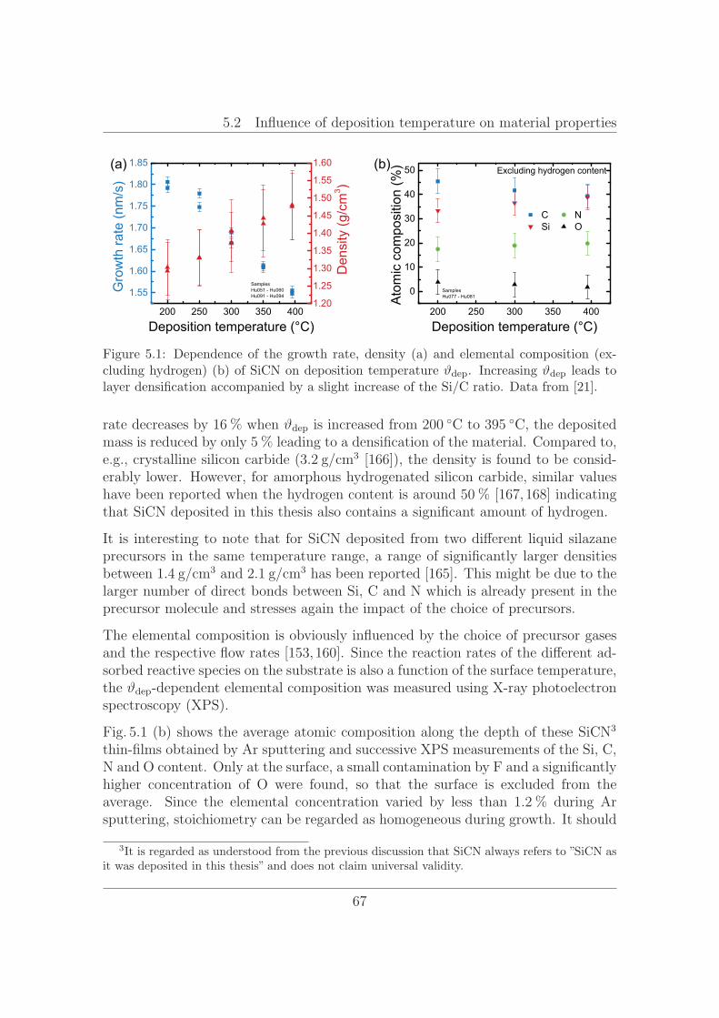
5.2 Influence of deposition temperature on material properties
200 250 300 350 400
1.55
1.60
1.65
1.70
1.75
1.80
1.85
Growthrate(nm/s)
Deposition temperature (°C)
(a)
1.20
1.25
1.30
1.35
1.40
1.45
1.50
1.55
1.60
Density(g/cm3 )
SamplesHu051 - Hu060Hu091 - Hu094
200 250 300 350 400
0
10
20
30
40
50
NO
Atomiccomposition(%)
Deposition temperature (°C)
CSi
SamplesHu077 - Hu081
(b) Excluding hydrogen content
Figure 5.1: Dependence of the growth rate, density (a) and elemental composition (ex-cluding hydrogen) (b) of SiCN on deposition temperature ϑ . Increasing ϑ leads tolayer densification accompanied by a slight increase of the Si/C ratio. Data from [21].
rate decreases by when ϑ is increased from ◦ to ◦ , the depositedmass is reduced by only leading to a densification of the material. Compared to,e.g., crystalline silicon carbide ( . / [166]), the density is found to be consid-erably lower. However, for amorphous hydrogenated silicon carbide, similar valueshave been reported when the hydrogen content is around [167,168] indicatingthat SiCN deposited in this thesis also contains a significant amount of hydrogen.
It is interesting to note that for SiCN deposited from two different liquid silazaneprecursors in the same temperature range, a range of significantly larger densitiesbetween . / and . / has been reported [165]. This might be due to thelarger number of direct bonds between Si, C and N which is already present in theprecursor molecule and stresses again the impact of the choice of precursors.
The elemental composition is obviously influenced by the choice of precursor gasesand the respective flow rates [153,160]. Since the reaction rates of the different ad-sorbed reactive species on the substrate is also a function of the surface temperature,the ϑ -dependent elemental composition was measured using X-ray photoelectronspectroscopy (XPS).
Fig. 5.1 (b) shows the average atomic composition along the depth of these SiCN3
thin-films obtained by Ar sputtering and successive XPS measurements of the Si, C,N and O content. Only at the surface, a small contamination by F and a significantlyhigher concentration of O were found, so that the surface is excluded from theaverage. Since the elemental concentration varied by less than . during Arsputtering, stoichiometry can be regarded as homogeneous during growth. It should
3It is regarded as understood from the previous discussion that SiCN always refers to ”SiCN asit was deposited in this thesis” and does not claim universal validity.
67
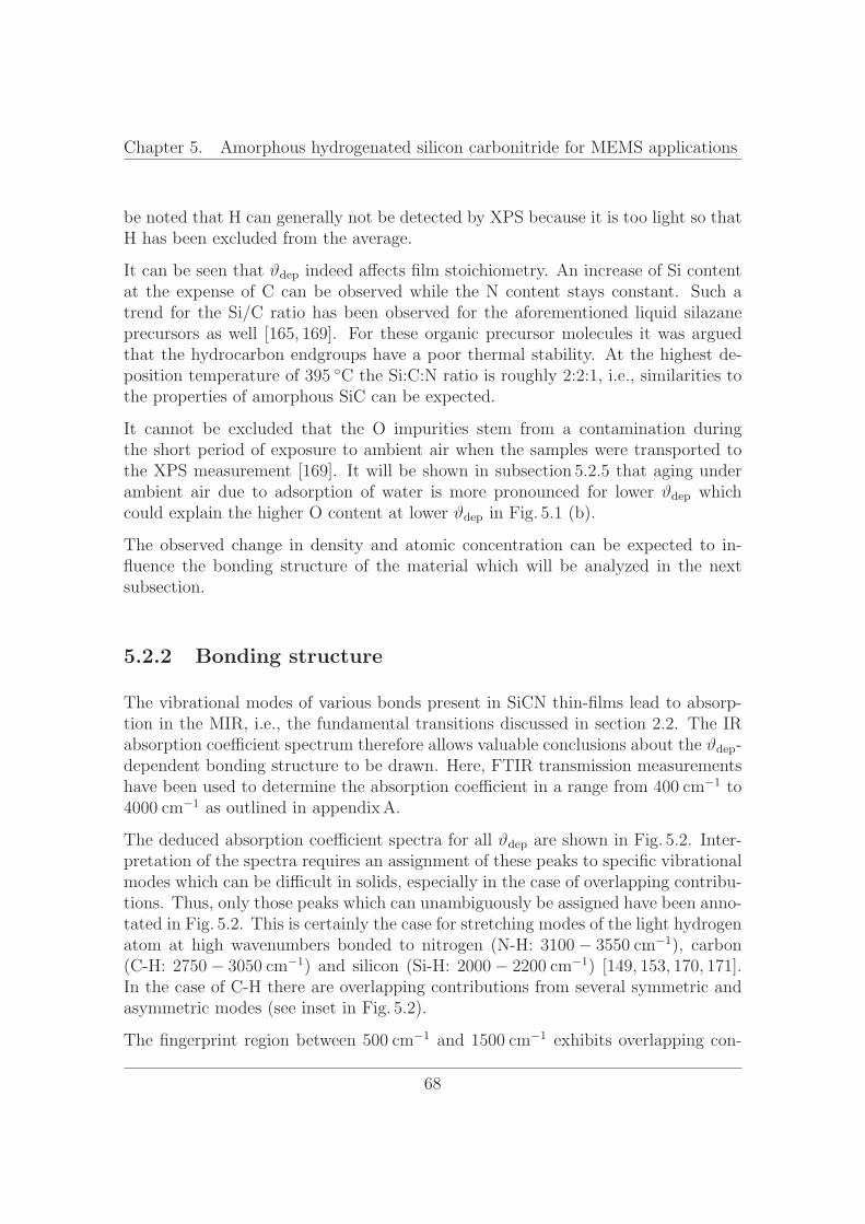
Chapter 5. Amorphous hydrogenated silicon carbonitride for MEMS applications
be noted that H can generally not be detected by XPS because it is too light so thatH has been excluded from the average.
It can be seen that ϑ indeed affects film stoichiometry. An increase of Si contentat the expense of C can be observed while the N content stays constant. Such atrend for the Si/C ratio has been observed for the aforementioned liquid silazaneprecursors as well [165, 169]. For these organic precursor molecules it was arguedthat the hydrocarbon endgroups have a poor thermal stability. At the highest de-position temperature of ◦ the Si:C:N ratio is roughly 2:2:1, i.e., similarities tothe properties of amorphous SiC can be expected.
It cannot be excluded that the O impurities stem from a contamination duringthe short period of exposure to ambient air when the samples were transported tothe XPS measurement [169]. It will be shown in subsection 5.2.5 that aging underambient air due to adsorption of water is more pronounced for lower ϑ whichcould explain the higher O content at lower ϑ in Fig. 5.1 (b).
The observed change in density and atomic concentration can be expected to in-fluence the bonding structure of the material which will be analyzed in the nextsubsection.
5.2.2 Bonding structure
The vibrational modes of various bonds present in SiCN thin-films lead to absorp-tion in the MIR, i.e., the fundamental transitions discussed in section 2.2. The IRabsorption coefficient spectrum therefore allows valuable conclusions about the ϑ -dependent bonding structure to be drawn. Here, FTIR transmission measurementshave been used to determine the absorption coefficient in a range from − to
− as outlined in appendixA.
The deduced absorption coefficient spectra for all ϑ are shown in Fig. 5.2. Inter-pretation of the spectra requires an assignment of these peaks to specific vibrationalmodes which can be difficult in solids, especially in the case of overlapping contribu-tions. Thus, only those peaks which can unambiguously be assigned have been anno-tated in Fig. 5.2. This is certainly the case for stretching modes of the light hydrogenatom at high wavenumbers bonded to nitrogen (N-H: − − ), carbon(C-H: − − ) and silicon (Si-H: − − ) [149, 153, 170, 171].In the case of C-H there are overlapping contributions from several symmetric andasymmetric modes (see inset in Fig. 5.2).
The fingerprint region between − and − exhibits overlapping con-
68
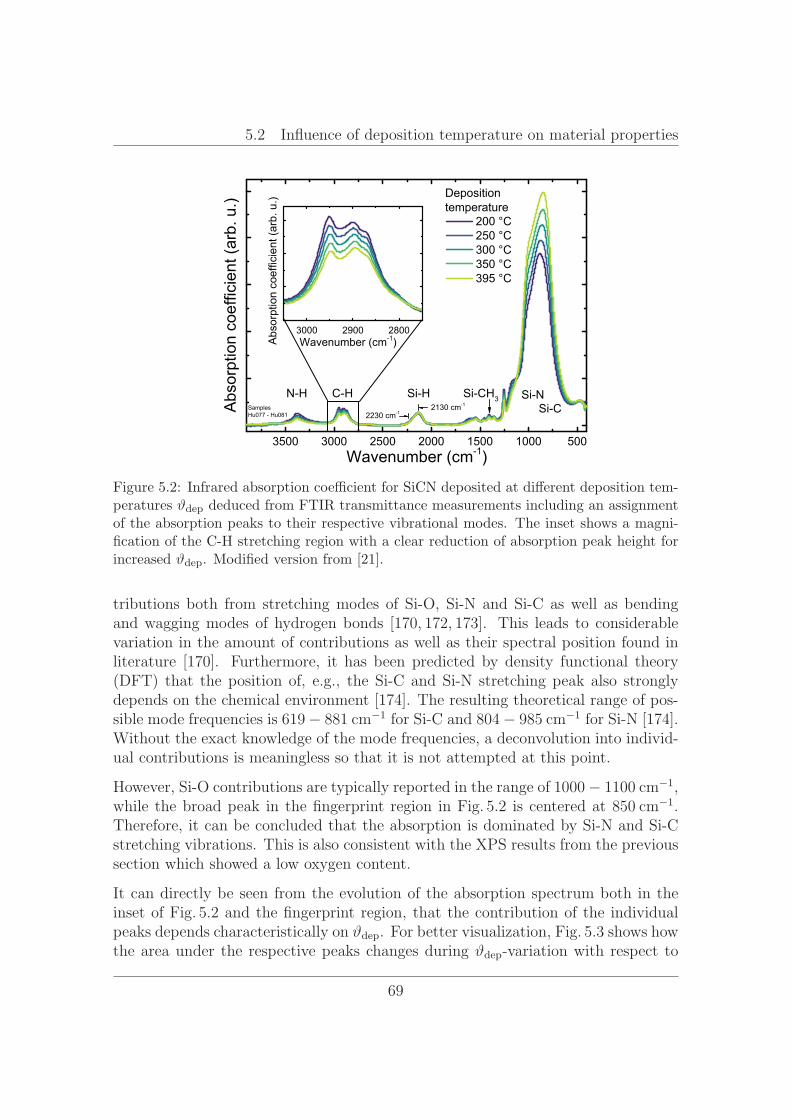
5.2 Influence of deposition temperature on material properties
3500 3000 2500 2000 1500 1000 500
Depositiontemperature
2230 cm-1 Si-CSi-NSi-CH3Si-HC-H
Absorptioncoefficient(arb.u.)
Wavenumber (cm-1)
200 °C250 °C300 °C350 °C395 °C
N-HSamplesHu077 - Hu081
2130 cm-1
3000 2900 2800
Absorptioncoefficient(arb.u.)
Wavenumber (cm-1)
Figure 5.2: Infrared absorption coefficient for SiCN deposited at different deposition tem-peratures ϑ deduced from FTIR transmittance measurements including an assignmentof the absorption peaks to their respective vibrational modes. The inset shows a magni-fication of the C-H stretching region with a clear reduction of absorption peak height forincreased ϑ . Modified version from [21].
tributions both from stretching modes of Si-O, Si-N and Si-C as well as bendingand wagging modes of hydrogen bonds [170, 172, 173]. This leads to considerablevariation in the amount of contributions as well as their spectral position found inliterature [170]. Furthermore, it has been predicted by density functional theory(DFT) that the position of, e.g., the Si-C and Si-N stretching peak also stronglydepends on the chemical environment [174]. The resulting theoretical range of pos-sible mode frequencies is − − for Si-C and − − for Si-N [174].Without the exact knowledge of the mode frequencies, a deconvolution into individ-ual contributions is meaningless so that it is not attempted at this point.
However, Si-O contributions are typically reported in the range of − − ,while the broad peak in the fingerprint region in Fig. 5.2 is centered at − .Therefore, it can be concluded that the absorption is dominated by Si-N and Si-Cstretching vibrations. This is also consistent with the XPS results from the previoussection which showed a low oxygen content.
It can directly be seen from the evolution of the absorption spectrum both in theinset of Fig. 5.2 and the fingerprint region, that the contribution of the individualpeaks depends characteristically on ϑ . For better visualization, Fig. 5.3 shows howthe area under the respective peaks changes during ϑ -variation with respect to
69
Chapter 5. Amorphous hydrogenated silicon carbonitride for MEMS applications
200 250 300 350 40060
80
100
120
140
160
SamplesHu077 - Hu081In
tegr.peakchange(%)
Deposition temperature (°C)
Si-C/Si-N peakSi-H peakC-H peakN-H peak
Figure 5.3: Change of the integrated absorption peaks from hydrogen-stretching modesand the Si-C/Si-N region with deposition temperature ϑ . The decrease of the formerand increase of the latter at higher ϑ points to a higher density due to a higher degreeof crosslinking. Modified version from [21].
ϑ , = ◦ . It can be seen that the strength of hydrogen stretching vibrationswith nitrogen and carbon decreases while the combined Si-C/Si-N vibrations fromthe fingerprint region increase when ϑ is increased. It is known that an increasedtemperature at the wafer surface leads to dissociation of hydrogen molecules afterbreaking of hydrogen terminated bonds [175]. This in turn leads to an increaseddegree of crosslinking between the remaining silicon, nitrogen and carbon atomsexplaining the stronger absorption in the fingerprint region. The observation isalso in accordance with the increased density at higher ϑ found in the previoussubsection.
In that sense, it is surprising that the same decreasing trend cannot be foundfor the Si-H peak. This is most probably due to the increased amount of sili-con at higher ϑ as evidenced by XPS. Some authors also assume a contributionfrom C≡N stretching vibrations in the same frequency range as the Si-H stretchingmode [146,158,169,173,176] which could then counteract a decrease in Si-H absorp-tion. However, it has been shown by DFT that C≡N should only be found above
− [174]. In Fig 5.2, the respective peak position is − indicatingthat it indeed stems from Si-H rather then C≡N stretching vibrations.
As already mentioned above, mode frequencies also depend on the chemical envi-ronment. Quite generally, one can say that a more electronegative bonding partnerleads to an increase of vibration frequencies as can be expected from the higher de-gree of polarity of the bonds [174]. As an example, DFT predicts an increase of theSi-H stretching mode frequency in X3-SiH moieties from − to −
when X changes from Si over C and N to O [174]. In that sense, the position of the
70
5.2 Influence of deposition temperature on material properties
Si-H stretching mode at − is in good agreement with the observation of alow oxygen content from XPS.
An interpretation of the small peak shifts with increasing ϑ is more difficult be-cause changes in the chemical environment are both due to the decreasing hydrogencontent and changes in the overall elemental composition known from XPS. Fur-thermore, it can’t be ruled out that small changes in peak position can also be dueto errors in the extraction procedure of absorption coefficient from transmittancespectra. For example, a small decrease of − of the Si-H stretching peak posi-tion can be observed. This is in principle in accordance with the reduced hydrogencontent at higher ϑ . However, from the increased silicon content at higher ϑone would expect a much larger peak shift [174]. At the same time, the peak positioncould be stabilized when silicon starts to form its bonds with sp2 hybrid orbitalssuch as in C=SiHC.
Summing up, the IR absorption spectrum of SiCN is rich in information. However,the sheer amount of possible bonds present in the material complicates its inter-pretation. Accurate theoretical predictions of peak positions as well as additionalinformation about the composition of the material are needed in order to preventwrong conclusions. However, from the variation in contribution of the individual,unambiguously assignable peaks it can be concluded that increasing deposition tem-perature ϑ leads to a higher degree of crosslinking between the Si, C and N atoms.This in turn can be expected to increase material stability.
5.2.3 Complex refractive index
It has been stated before that the refractive index is among the most interestingproperties which influences suitability of SiCN for optical MEMS applications. Asthe complex refractive index n of a material results from the polarization responseof the dipoles within the material [177], it can be expected that the material densityaffects n.
In previous studies the refractive index of SiCN has been determined both fromtransmittance and/or reflectance measurements [144,165,172,178,179] and spectro-scopic ellipsometry (SE) [146, 147, 149, 153, 154, 157, 180]. SE is a suitable measure-ment technique to determine the refractive index and thickness of optically thin filmssimultaneously. Compared to intensity measurements such as reflectance and trans-mittance, SE yields a complex number as the measurand, i.e., two values insteadof one per wavelength for the unknown quantities. However, in order to extractthe desired information, an optical model for the thin-film stack under study hasto be assumed [181]. Good results can only be obtained, if the chosen refractive
71
Chapter 5. Amorphous hydrogenated silicon carbonitride for MEMS applications
index model function describes the actual refractive index accurately over the wholemeasured wavelength range.
Surprisingly, previous studies which have employed SE often did not specify themodel used to describe SiCN [146, 147, 157, 180]. Other authors have used a seriesof Lorentz oscillators [149], a combination of a Cauchy dispersion with a Lorentzoscillator [153] or a so-called Forouhi-Bloomer model [154]. While the last two maydescribe the refractive index dispersion reasonably well over a certain wavelengthrange they are intrinsically unphysical because they are not Kramers–Kronig con-sistent [181]. Furthermore, none of these models can describe a spectral range freeof absorption below the band gap E as it would be expected for a semiconductor.It can therefore be stated that there is no consensus on how to correctly model theoptical properties of SiCN.
The Tauc-Lorentz model has specifically been developed for describing the complexrefractive index n of amorphous semiconductors in the vicinity of their optical gapE [182,183]. It models the imaginary part of the dielectric function ε2 as zero belowand ε2 ∝ (hν−E )2/(hν)2 above E , following theoretical predictions for amorphousgermanium [184]. For higher energies, ε2 adopts the shape of a Lorentz-oscillator re-presenting all optical transitions at higher energies and assuring that hν→∞ ε2 = 0.The real part of the dielectric function ε1 is then obtained by Kramers–Kronigintegration so that the model is intrinsically Kramers–Kronig consistent [182]:
ε2, (hν) =
{βE0γ(hν−E )2
((hν)2−E20)
2+γ2(hν)2· 1hν
hν > E
0 hν ≤ E(5.1)
The additional fit parameters apart from the optical gap E are the energetic positionE0, broadening γ and amplitude β of the Lorentz-oscillator part.
Fig. 5.4 shows spectra of the ellipsometric angles Ψ and Δ from a variable angle SEmeasurement of a SiCN thin-film deposited at ◦ . The data can consistentlybe fitted over the whole spectral range from to (i.e. comprisingthe full NIR relevant for later application in an FPI) using the aforementionedTauc-Lorentz model. Inclusion of a surface roughness layer did not significantlyimprove fit quality so that it was omitted to reduce the number of free fit parameters.Similarly, more advanced models such as the Cody-Lorentz model, which also allowsmodeling of sub-band gap absorption in an Urbach tail (but therefore needs morefit parameters) [185], did not improve the fits.
The resulting dispersion of the real part of the refractive index is plotted in Fig. 5.5 (a)for the used deposition temperatures ϑ . It can be seen that ϑ mainly causesan offset in refractive index without affecting the shape of the dispersion. This in-
72
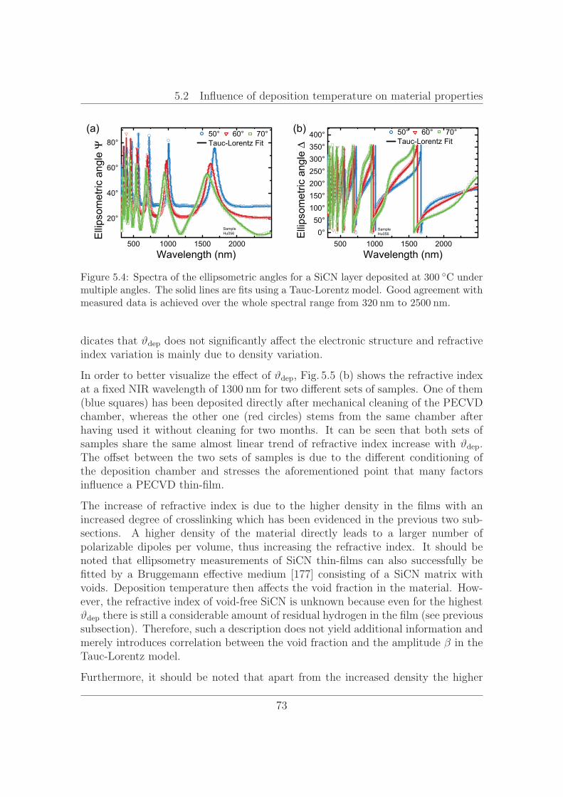
5.2 Influence of deposition temperature on material properties
500 1000 1500 2000
20°
40°
60°
80°
Ellipsometricangle
Ψ
Wavelength (nm)
50° 60° 70°Tauc-Lorentz Fit
SampleHu056
(a)
500 1000 1500 20000°50°100°150°200°250°300°350°400°
(b)
Ellipsometricangle
Δ
Wavelength (nm)
50° 60° 70°Tauc-Lorentz Fit
SampleHu056
Figure 5.4: Spectra of the ellipsometric angles for a SiCN layer deposited at ◦ undermultiple angles. The solid lines are fits using a Tauc-Lorentz model. Good agreement withmeasured data is achieved over the whole spectral range from to .
dicates that ϑ does not significantly affect the electronic structure and refractiveindex variation is mainly due to density variation.
In order to better visualize the effect of ϑ , Fig. 5.5 (b) shows the refractive indexat a fixed NIR wavelength of for two different sets of samples. One of them(blue squares) has been deposited directly after mechanical cleaning of the PECVDchamber, whereas the other one (red circles) stems from the same chamber afterhaving used it without cleaning for two months. It can be seen that both sets ofsamples share the same almost linear trend of refractive index increase with ϑ .The offset between the two sets of samples is due to the different conditioning ofthe deposition chamber and stresses the aforementioned point that many factorsinfluence a PECVD thin-film.
The increase of refractive index is due to the higher density in the films with anincreased degree of crosslinking which has been evidenced in the previous two sub-sections. A higher density of the material directly leads to a larger number ofpolarizable dipoles per volume, thus increasing the refractive index. It should benoted that ellipsometry measurements of SiCN thin-films can also successfully befitted by a Bruggemann effective medium [177] consisting of a SiCN matrix withvoids. Deposition temperature then affects the void fraction in the material. How-ever, the refractive index of void-free SiCN is unknown because even for the highestϑ there is still a considerable amount of residual hydrogen in the film (see previoussubsection). Therefore, such a description does not yield additional information andmerely introduces correlation between the void fraction and the amplitude β in theTauc-Lorentz model.
Furthermore, it should be noted that apart from the increased density the higher
73
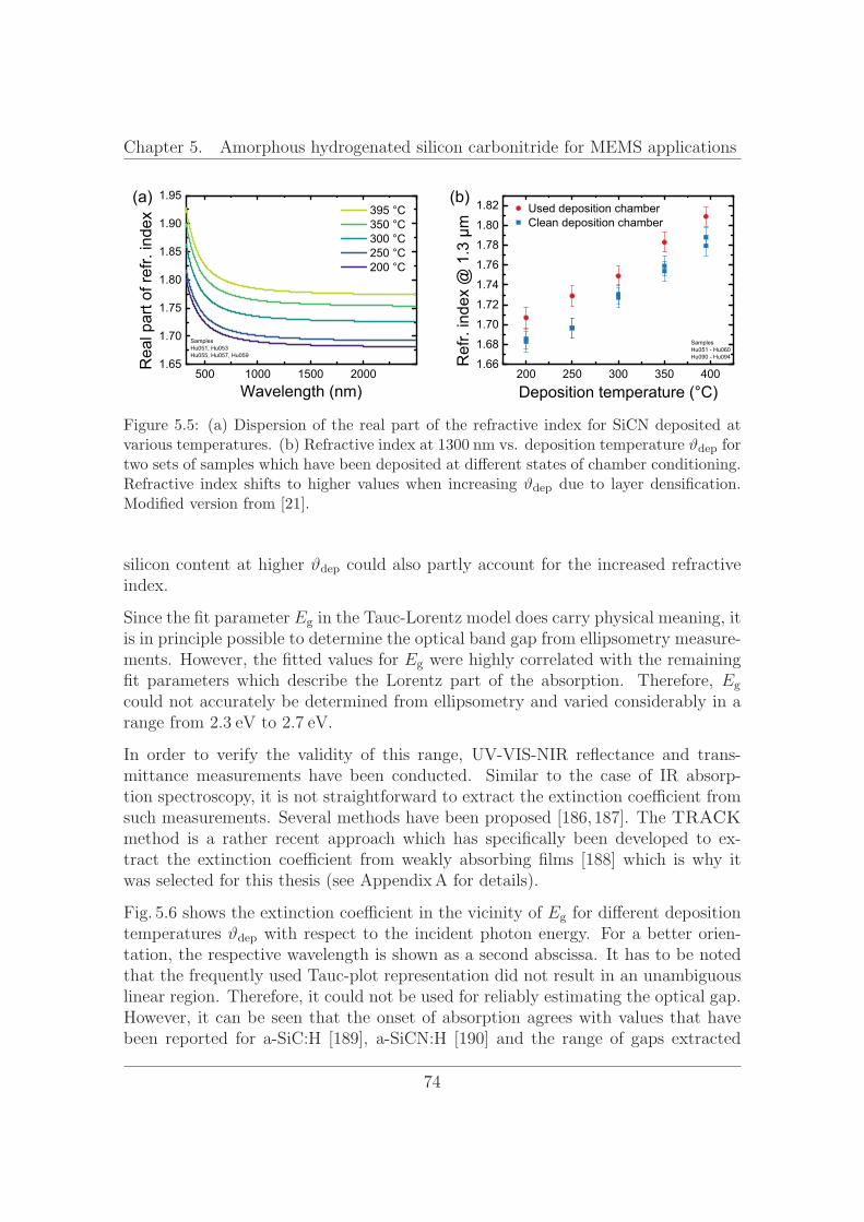
Chapter 5. Amorphous hydrogenated silicon carbonitride for MEMS applications
500 1000 1500 20001.65
1.70
1.75
1.80
1.85
1.90
1.95
Realpartofrefr.index
Wavelength (nm)
395 °C350 °C300 °C250 °C200 °C
SamplesHu051, Hu053Hu055, Hu057, Hu059
(a)
200 250 300 350 4001.66
1.68
1.70
1.72
1.74
1.76
1.78
1.80
1.82
Deposition temperature (°C)
Used deposition chamberClean deposition chamber
SamplesHu051 - Hu060Hu090 - Hu094
(b)
Figure 5.5: (a) Dispersion of the real part of the refractive index for SiCN deposited atvarious temperatures. (b) Refractive index at vs. deposition temperature ϑ fortwo sets of samples which have been deposited at different states of chamber conditioning.Refractive index shifts to higher values when increasing ϑ due to layer densification.Modified version from [21].
silicon content at higher ϑ could also partly account for the increased refractiveindex.
Since the fit parameter E in the Tauc-Lorentz model does carry physical meaning, itis in principle possible to determine the optical band gap from ellipsometry measure-ments. However, the fitted values for E were highly correlated with the remainingfit parameters which describe the Lorentz part of the absorption. Therefore, Ecould not accurately be determined from ellipsometry and varied considerably in arange from . to . .
In order to verify the validity of this range, UV-VIS-NIR reflectance and trans-mittance measurements have been conducted. Similar to the case of IR absorp-tion spectroscopy, it is not straightforward to extract the extinction coefficient fromsuch measurements. Several methods have been proposed [186,187]. The TRACKmethod is a rather recent approach which has specifically been developed to ex-tract the extinction coefficient from weakly absorbing films [188] which is why itwas selected for this thesis (see AppendixA for details).
Fig. 5.6 shows the extinction coefficient in the vicinity of E for different depositiontemperatures ϑ with respect to the incident photon energy. For a better orien-tation, the respective wavelength is shown as a second abscissa. It has to be notedthat the frequently used Tauc-plot representation did not result in an unambiguouslinear region. Therefore, it could not be used for reliably estimating the optical gap.However, it can be seen that the onset of absorption agrees with values that havebeen reported for a-SiC:H [189], a-SiCN:H [190] and the range of gaps extracted
74
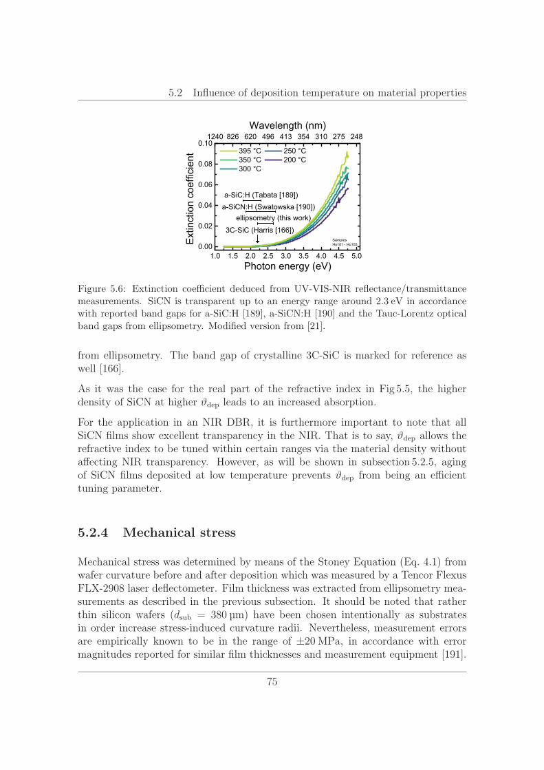
5.2 Influence of deposition temperature on material properties
1.0 1.5 2.0 2.5 3.0 3.5 4.0 4.5 5.00.00
0.02
0.04
0.06
0.08
0.101240 826 620 496 413 354 310 275 248
Wavelength (nm)
Extinctioncoefficient
Photon energy (eV)
395 °C 250 °C350 °C 200 °C300 °C
a-SiC:H (Tabata [189])a-SiCN:H (Swatowska [190])
ellipsometry (this work)
3C-SiC (Harris [166])SamplesHu101 - Hu105
Figure 5.6: Extinction coefficient deduced from UV-VIS-NIR reflectance/transmittancemeasurements. SiCN is transparent up to an energy range around . in accordancewith reported band gaps for a-SiC:H [189], a-SiCN:H [190] and the Tauc-Lorentz opticalband gaps from ellipsometry. Modified version from [21].
from ellipsometry. The band gap of crystalline 3C-SiC is marked for reference aswell [166].
As it was the case for the real part of the refractive index in Fig 5.5, the higherdensity of SiCN at higher ϑ leads to an increased absorption.
For the application in an NIR DBR, it is furthermore important to note that allSiCN films show excellent transparency in the NIR. That is to say, ϑ allows therefractive index to be tuned within certain ranges via the material density withoutaffecting NIR transparency. However, as will be shown in subsection 5.2.5, agingof SiCN films deposited at low temperature prevents ϑ from being an efficienttuning parameter.
5.2.4 Mechanical stress
Mechanical stress was determined by means of the Stoney Equation (Eq. 4.1) fromwafer curvature before and after deposition which was measured by a Tencor FlexusFLX-2908 laser deflectometer. Film thickness was extracted from ellipsometry mea-surements as described in the previous subsection. It should be noted that ratherthin silicon wafers (d = ) have been chosen intentionally as substratesin order increase stress-induced curvature radii. Nevertheless, measurement errorsare empirically known to be in the range of ± , in accordance with errormagnitudes reported for similar film thicknesses and measurement equipment [191].
75
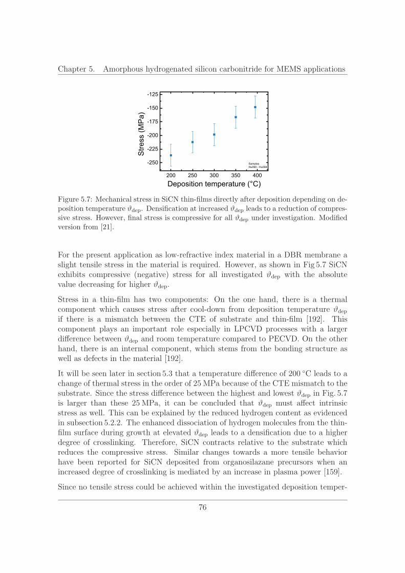
Chapter 5. Amorphous hydrogenated silicon carbonitride for MEMS applications
200 250 300 350 400
-250
-225
-200
-175
-150
-125
Stress(MPa)
Deposition temperature (°C)
SamplesHu090 - Hu094
Figure 5.7: Mechanical stress in SiCN thin-films directly after deposition depending on de-position temperature ϑ . Densification at increased ϑ leads to a reduction of compres-sive stress. However, final stress is compressive for all ϑ under investigation. Modifiedversion from [21].
For the present application as low-refractive index material in a DBR membrane aslight tensile stress in the material is required. However, as shown in Fig 5.7 SiCNexhibits compressive (negative) stress for all investigated ϑ with the absolutevalue decreasing for higher ϑ .
Stress in a thin-film has two components: On the one hand, there is a thermalcomponent which causes stress after cool-down from deposition temperature ϑif there is a mismatch between the CTE of substrate and thin-film [192]. Thiscomponent plays an important role especially in LPCVD processes with a largerdifference between ϑ and room temperature compared to PECVD. On the otherhand, there is an internal component, which stems from the bonding structure aswell as defects in the material [192].
It will be seen later in section 5.3 that a temperature difference of ◦ leads to achange of thermal stress in the order of because of the CTE mismatch to thesubstrate. Since the stress difference between the highest and lowest ϑ in Fig. 5.7is larger than these , it can be concluded that ϑ must affect intrinsicstress as well. This can be explained by the reduced hydrogen content as evidencedin subsection 5.2.2. The enhanced dissociation of hydrogen molecules from the thin-film surface during growth at elevated ϑ leads to a densification due to a higherdegree of crosslinking. Therefore, SiCN contracts relative to the substrate whichreduces the compressive stress. Similar changes towards a more tensile behaviorhave been reported for SiCN deposited from organosilazane precursors when anincreased degree of crosslinking is mediated by an increase in plasma power [159].
Since no tensile stress could be achieved within the investigated deposition temper-
76
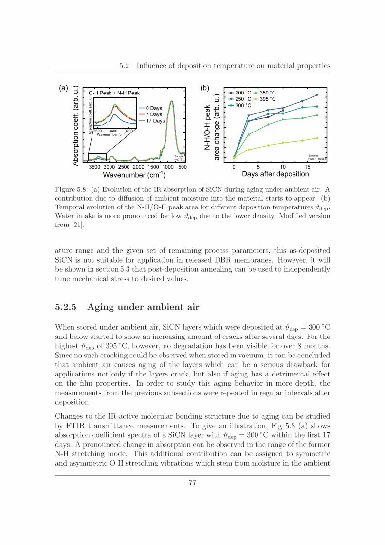
5.2 Influence of deposition temperature on material properties
3500 3000 2500 2000 1500 1000 500Absorptioncoeff.(arb.u.)
Wavenumber (cm-1)
0 Days7 Days17 Days
SampleHu079
O-H Peak + N-H Peak(a)
3600 3400 3200
Absorptioncoeff.(arb.u.)
Wavenumber (cm-1)
0 5 10 15
N-H/O-Hpeak
areachange(arb.u.)
Days after deposition
200 °C 350 °C250 °C 395 °C300 °C
SamplesHu077 - Hu081
(b)
Figure 5.8: (a) Evolution of the IR absorption of SiCN during aging under ambient air. Acontribution due to diffusion of ambient moisture into the material starts to appear. (b)Temporal evolution of the N-H/O-H peak area for different deposition temperatures ϑ .Water intake is more pronounced for low ϑ due to the lower density. Modified versionfrom [21].
ature range and the given set of remaining process parameters, this as-depositedSiCN is not suitable for application in released DBR membranes. However, it willbe shown in section 5.3 that post-deposition annealing can be used to independentlytune mechanical stress to desired values.
5.2.5 Aging under ambient air
When stored under ambient air, SiCN layers which were deposited at ϑ = ◦
and below started to show an increasing amount of cracks after several days. For thehighest ϑ of ◦ , however, no degradation has been visible for over 8 months.Since no such cracking could be observed when stored in vacuum, it can be concludedthat ambient air causes aging of the layers which can be a serious drawback forapplications not only if the layers crack, but also if aging has a detrimental effecton the film properties. In order to study this aging behavior in more depth, themeasurements from the previous subsections were repeated in regular intervals afterdeposition.
Changes to the IR-active molecular bonding structure due to aging can be studiedby FTIR transmittance measurements. To give an illustration, Fig. 5.8 (a) showsabsorption coefficient spectra of a SiCN layer with ϑ = ◦ within the first 17days. A pronounced change in absorption can be observed in the range of the formerN-H stretching mode. This additional contribution can be assigned to symmetricand asymmetric O-H stretching vibrations which stem from moisture in the ambient
77
Chapter 5. Amorphous hydrogenated silicon carbonitride for MEMS applications
air after having diffused into the layer. Such behavior of amorphous hydrogenatedPECVD films has been observed for SiC [193] and SiCN [153].
After diffusion into the thin-film, water could either be only adsorbed into the voidswithin the material or react further with hydrogen-terminated bonds to form ahydroxyl group. Both mechanisms would lead to a broad absorption in this spectralrange [194–196]. Indications for both mechanisms are present. For instance, allspectra show a slightly reduced Si-H peak which points towards an oxidation reactionof Si-H to Si-O-H [153]. Additionally, a shoulder at − starts to appear whichcould be due to a further reaction to Si-O-Si. At the same time, a second smallshoulder at around − indicates the presence of a bending mode in purelyadsorbed water [196]. However, it has to be noted that these are very small changeswhich are certainly not strong enough to assign a specific mechanism with confidence,especially given small variations in the spectra due to the fitting procedure.
Since the change in the N-H/O-H peak area is a measure for diffusion of water intothe SiCN film, it can be used to monitor its temporal evolution. This is illustratedin Fig. 5.8 (b) within a time period up to 17 days after deposition. Apparently,such diffusion of ambient moisture occurs for all deposited SiCN layers. However,those SiCN layers which start to crack after a while, i.e., those deposited at ◦
and below are more permeable for water. This can be understood by their moreopen, porous structure due to the reduced density. For the case of amorphoussilicon oxycarbonitride (SiOCN), it has been found that densities below /(as it is also the case for SiCN here) result in inefficient barrier properties againstmoisture [197].
The previous subsections showed that the optical and mechanical properties aredirectly linked to the bonding structure of the material. Therefore, it can be expectedthat they are influenced by water intake in ambient air as well. Fig. 5.9 shows thechanges in film thickness, refractive index and stress within 12 days for differentdeposition temperatures ϑ . It can be seen that aging causes swelling of the layersaccompanied by a reduction of refractive index. Note that swelling is plotted asa percentage change because the initial thickness differed and thicker layers canincorporate more water. Again, for ϑ = ◦ and above these changes arebarely visible while for lower ϑ thickness increases up to and refractive indexdecreases by up to -0.014 for T = ◦ , in accordance with the findings fromFig. 5.8. In the case of mechanical stress, aging leads to an increase of compressivestress of more than for the lower ϑ .
It can be expected that the dipole moments of adsorbed water in the pore walls ofthe film lead to a repulsive force [198] which results in swelling of the layers. As
78
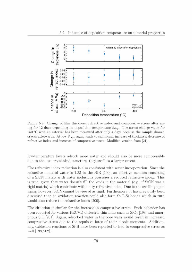
5.2 Influence of deposition temperature on material properties
-0.03-0.02-0.010.000.01
01234
200 300 400-250-200-150-100-500
Changein
refract.index
Changein
thickness(%)
within 12 days after deposition
Changein
stress(MPa)
Deposition temperature (°C)
SamplesHu051 - Hu060Hu091 - Hu094
*
Figure 5.9: Change of film thickness, refractive index and compressive stress after ag-ing for 12 days depending on deposition temperature ϑ . The stress change value for
◦ with an asterisk has been measured after only 4 days because the sample showedcracks afterwards. At low ϑ , aging leads to significant increase of thickness, decrease ofrefractive index and increase of compressive stress. Modified version from [21].
low-temperature layers adsorb more water and should also be more compressibledue to the less crosslinked structure, they swell to a larger extent.
The refractive index reduction is also consistent with water incorporation. Since therefractive index of water is 1.33 in the NIR [199], an effective medium consistingof a SiCN matrix with water inclusions possesses a reduced refractive index. Thisis true, given that water doesn’t fill the voids in the material (e.g. if SiCN was arigid matrix) which contribute with unity refractive index. Due to the swelling uponaging, however, SiCN cannot be viewed as rigid. Furthermore, it has previously beendiscussed that an oxidation reaction could also form Si-O-Si bonds which in turnwould also reduce the refractive index [200].
The situation is similar for the increase in compressive stress. Such behavior hasbeen reported for various PECVD dielectric thin-films such as SiO2 [198] and amor-phous SiC [201]. Again, adsorbed water in the pore walls would result in increasedcompressive stress due to the repulsive force of their dipole moments. Addition-ally, oxidation reactions of Si-H have been reported to lead to compressive stress aswell [198,202].
79
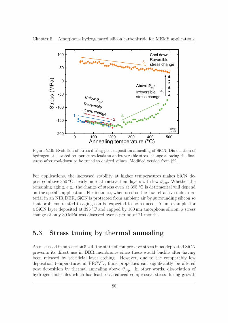
Chapter 5. Amorphous hydrogenated silicon carbonitride for MEMS applications
0 100 200 300 400 500-200
-150
-100
-50
0
50
100
5.
4.
3.2.
Cool down:Reversible stress change
Above dep:
Irreversible stress change
Stre
ss (M
Pa)
Annealing temperature (°C)
SampleHu106
Below dep:Reversible stress change1.
Figure 5.10: Evolution of stress during post-deposition annealing of SiCN. Dissociation ofhydrogen at elevated temperatures leads to an irreversible stress change allowing the finalstress after cool-down to be tuned to desired values. Modified version from [22].
For applications, the increased stability at higher temperatures makes SiCN de-posited above ◦ clearly more attractive than layers with low ϑ . Whether theremaining aging, e.g., the change of stress even at ◦ is detrimental will dependon the specific application. For instance, when used as the low-refractive index ma-terial in an NIR DBR, SiCN is protected from ambient air by surrounding silicon sothat problems related to aging can be expected to be reduced. As an example, fora SiCN layer deposited at ◦ and capped by amorphous silicon, a stresschange of only was observed over a period of 21 months.
5.3 Stress tuning by thermal annealing
As discussed in subsection 5.2.4, the state of compressive stress in as-deposited SiCNprevents its direct use in DBR membranes since these would buckle after havingbeen released by sacrificial layer etching. However, due to the comparably lowdeposition temperatures in PECVD, films properties can significantly be alteredpost deposition by thermal annealing above ϑ . In other words, dissociation ofhydrogen molecules which has lead to a reduced compressive stress during growth
80
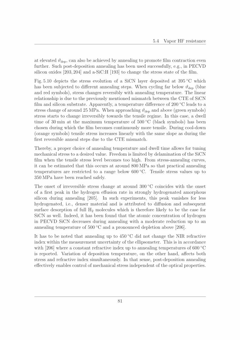
5.4 Vapor HF resistance
at elevated ϑ , can also be achieved by annealing to promote film contraction evenfurther. Such post-deposition annealing has been used successfully, e.g., in PECVDsilicon oxides [203,204] and a-SiC:H [193] to change the stress state of the film.
Fig. 5.10 depicts the stress evolution of a SiCN layer deposited at ◦ whichhas been subjected to different annealing steps. When cycling far below ϑ (blueand red symbols), stress changes reversibly with annealing temperature. The linearrelationship is due to the previously mentioned mismatch between the CTE of SiCNfilm and silicon substrate. Apparently, a temperature difference of ◦ leads to astress change of around . When approaching ϑ and above (green symbols)stress starts to change irreversibly towards the tensile regime. In this case, a dwelltime of at the maximum temperature of ◦ (black symbols) has beenchosen during which the film becomes continuously more tensile. During cool-down(orange symbols) tensile stress increases linearly with the same slope as during thefirst reversible anneal steps due to the CTE mismatch.
Thereby, a proper choice of annealing temperature and dwell time allows for tuningmechanical stress to a desired value. Freedom is limited by delamination of the SiCNfilm when the tensile stress level becomes too high. From stress-annealing curves,it can be estimated that this occurs at around so that practical annealingtemperatures are restricted to a range below ◦ . Tensile stress values up to
have been reached safely.
The onset of irreversible stress change at around ◦ coincides with the onsetof a first peak in the hydrogen effusion rate in strongly hydrogenated amorphoussilicon during annealing [205]. In such experiments, this peak vanishes for lesshydrogenated, i.e., denser material and is attributed to diffusion and subsequentsurface desorption of full H2 molecules which is therefore likely to be the case forSiCN as well. Indeed, it has been found that the atomic concentration of hydrogenin PECVD SiCN decreases during annealing with a moderate reduction up to anannealing temperature of ◦ and a pronounced depletion above [206].
It has to be noted that annealing up to ◦ did not change the NIR refractiveindex within the measurement uncertainty of the ellipsometer. This is in accordancewith [206] where a constant refractive index up to annealing temperatures of ◦
is reported. Variation of deposition temperature, on the other hand, affects bothstress and refractive index simultaneously. In that sense, post-deposition annealingeffectively enables control of mechanical stress independent of the optical properties.
81
Chapter 5. Amorphous hydrogenated silicon carbonitride for MEMS applications
0 20 40 60 80 100 120 140 160 180
-2
0
2
4
6
8
10
12
Slow etching
Thicknessdecrease(nm)
Etch time (min)
/ as prepared/ annealed
Fastetchi
ng
SamplesHu135, Hu136
(a)
0 20 40 60 80 100 120 140 160 1802468101214161820222426
Slow etching
Roughnessincrease(nm)
Etch time (min)
/ as prepared/ annealed
Fast etching
SamplesHu135, Hu136
(b)
Figure 5.11: (a) Thickness decrease and (b) roughness increase for as-prepared and an-nealed ( ◦ ) SiCN when subjected to vapor HF etching. The process denoted as ”fast”uses a considerably higher pressure and water catalyst supply rate than the ”slow”process.SiCN shows almost perfect resistance against HF etching with an etch rate < . / .Straight lines between data points serve as a guide to the eye only.
5.4 Vapor HF resistance
So far, etch resistance of SiCN and related materials has been studied for wet etching.For example, it has been found that silane based SiOCN etches at / inconcentrated HF diluted in ethanol and at . / in phosphoric acid [200]. ForSiCN from an organic silazane precursor, films did not etch in buffered oxide etch(BOE), given that the carbon content was high enough [159]. This behavior can beexpected from a mixture material point of view, since a-SiC is more stable in wetHF than a-SiNx [129,130].
As SiCN has not been used for MEMS fabrication so far, vapor HF etching, being aspecial process step for fabrication of freestanding structures, has not been of inter-est. Resistance to wet HF does not necessarily imply the same for the vapor phase.For instance, LPCVD Si3N4 etches only slowly in HF diluted in H2O ( . / )and even slower in BOE ( . / ), whereas it is attacked by vapor HF and forms(NH4)2SiF6 residues [128].
The SiCN layers in this thesis were unstable both in BOE (7:1 from Microchemicalsfor ) and vapor HF when deposited at ◦ and below. At ϑ = ◦
they were not attacked in BOE but showed a strong increase in surface roughnessafter etching in vapor. Given the knowledge from the previous sections, this in-crease in etch resistance can be attributed to the increased density and degree ofcrosslinking [159].
A detailed analysis of vapor HF etch behavior was conducted for SiCN deposited
82
5.5 Other properties relevant to MEMS fabrication
at ◦ since these turned out to be most favorable for application regardingtheir aging behavior and the only ones which were actually vapor HF resistant.Additionally, in order to check whether post-deposition annealing can improve etchresistance, a SiCN film annealed up to ◦ has been etched simultaneously. Twodifferent process conditions were chosen for illustrating purposes. The ”fast” processwith a high pressure and a high water supply rate etches thermal oxide4 with a rateof roughly / . That is to say, the process is considerably more aggressivethan necessary for a MEMS release and would certainly lead to stiction for manydevices. The ”slow” process on the other hand etches dense thermal oxide (TO)at only / . SiCN thickness has been measured ellipsometrically both beforeand after vapor HF etching for different periods. After etching, a surface roughnesslayer, modeled as an effective medium with 50% air and 50% SiCN, had to be usedin the fits.
Fig. 5.11 shows how SiCN thickness decreases and surface roughness increases duringetching. First, it can be noted that under all conditions, SiCN is extremely stable atan average etch rate < . / even for the aggressive etch process. Second, theannealed sample etches with roughly of the etch rate without annealing, proba-bly due to an even higher degree of crosslinking after hydrogen molecule dissociation.Third, the increase of roughness layer thickness for the fast process is approximatelydouble the layer thickness loss. Accordingly, the HF atmosphere rather leads to asurface roughening than actual etching of the material. For all practical purposes,SiCN deposited at ◦ can therefore be regarded as HF resistant.
5.5 Other properties relevant to
MEMS fabrication
A number of other experiments have been conducted to demonstrate the suitabi-lity of SiCN as a MEMS material which, however, were of minor importance forthe present application as an HF resistant, tensile, low-refractive index material.They will therefore only be presented briefly at this point. All results refer to SiCNdeposited at ϑ = ◦ .
Anisotropic structuring of SiCN was achieved by inductively coupled plasma etchingwith several different gas mixtures of SiF6, C4F8, O2 and He. Figure 5.12 shows ascanning electron microscopy (SEM) cross section of a SiCN thin-film deposited ona wafer after plasma etching with a photoresist mask and a standard recipe used inthis thesis for etching Si/SiCN DBRs. The resulting edge has an angle of ◦. Since
4Commonly, silicon oxides are simply called oxides in MEMS technology.
83
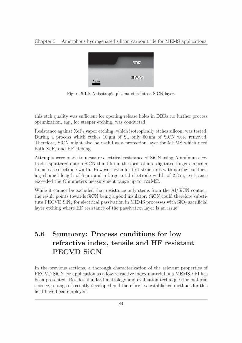
Chapter 5. Amorphous hydrogenated silicon carbonitride for MEMS applications
Figure 5.12: Anisotropic plasma etch into a SiCN layer.
this etch quality was sufficient for opening release holes in DBRs no further processoptimization, e.g., for steeper etching, was conducted.
Resistance against XeF2 vapor etching, which isotropically etches silicon, was tested.During a process which etches of Si, only of SiCN were removed.Therefore, SiCN might also be useful as a protection layer for MEMS which needboth XeF2 and HF etching.
Attempts were made to measure electrical resistance of SiCN using Aluminum elec-trodes sputtered onto a SiCN thin-film in the form of interdigitated fingers in orderto increase electrode width. However, even for test structures with narrow conduct-ing channel length of and a large total electrode width of . , resistanceexceeded the Ohmmeters measurement range up to 120MΩ.
While it cannot be excluded that resistance only stems from the Al/SiCN contact,the result points towards SiCN being a good insulator. SiCN could therefore substi-tute PECVD SiNx for electrical passivation in MEMS processes with SiO2 sacrificiallayer etching where HF resistance of the passivation layer is an issue.
5.6 Summary: Process conditions for low
refractive index, tensile and HF resistant
PECVD SiCN
In the previous sections, a thorough characterization of the relevant properties ofPECVD SiCN for application as a low-refractive index material in a MEMS FPI hasbeen presented. Besides standard metrology and evaluation techniques for materialscience, a range of recently developed and therefore less established methods for thisfield have been employed.
84
5.6 Summary: Process conditions for PECVD SiCN
These include
• extracting the IR absorption coefficient by an iterative, Kramers–Kronig con-sistent method from FTIR transmittance spectra [207].
• the TRACK method for determining the extinction coefficient of weakly ab-sorbing films in the visible from reflectance/transmittance measurements [188].
Furthermore, it has been established that the refractive index of PECVD SiCN canbe modeled over a broad spectral range from to by the Tauc-Lorentzmodel, which obeys Kramers–Kronig relations and is based on an actual physicalmodel for amorphous semiconductors.
In summary, it has been illustrated that the choice of deposition temperature ϑprofoundly affects the resulting material properties of PECVD SiCN. The under-lying responsible mechanism has been identified as being the reduction of residualhydrogen content and resulting increased crosslinking between the Si, C and N atomswhen hydrogen molecules can dissociate from the surface at elevated temperatures.This densifies the layers, increases the refractive index and reduces the absolutecompressive stress. In that sense, ϑ can be seen as a tuning parameter for theseproperties.
However, both an insufficient resistance against aging and vapor HF etching at lowdeposition temperatures ϑ prevent ϑ from being a parameter to be chosenfreely. Nevertheless, at ϑ = ◦ the degree of crosslinking between Si, C andN is sufficient for a stable material.
Combined with the refractive index being considerably lower than it is the casefor materials with comparable vapor HF resistance and the additional mechanicalfreedom due to an independently tunable tensile stress by post-deposition anneal-ing, PECVD SiCN possesses a unique set of properties for application in MOEMSdevices. Moreover, the refractive index of 1.8 reaches the range which has beenidentified in the previous chapter as being ideal for a five layer DBR offering highreflectance over the full first FSR.
It is important to stress again that the results regarding the ϑ -dependence of theserequired properties cover only a small subspace of possible deposition parametercombinations. Since the underlying mechanism of an increased degree of crosslinkingdue to hydrogen molecule dissociation is very general, it can be expected that thesame trends also hold true for other sets of deposition parameters. In particular, itwould not be surprising if there was still some room for, e.g., an increase in nitrogencontent by changing the precursor flow ratios and thereby even lower refractiveindices without negatively affecting HF stability.
85

Chapter 5. Amorphous hydrogenated silicon carbonitride for MEMS applications
Alternatively, PECVD offers other means for providing energy during the growthprocess, namely ion bombardment. Therefore, it can be expected that plasma power,frequency and substrate bias voltage [176] can also serve as effective tuning param-eters with similar trends as those observed for deposition temperature variation.Since the refractive index resulting from the current set of parameters was alreadysatisfactory, no further attempts for optimization were made during this thesis.Therefore, the interesting question regarding a lower limit for the refractive indexof HF-resistant SiCN remains open for future research.
86
Chapter 6
Design and fabrication of nearinfrared Fabry-Perotinterferometers with silicon/siliconcarbonitride based Bragg mirrors
The previous chapter has shown that SiCN possesses all required properties for alow-refractive index material in a five layer DBR with high reflectance over thefull first FSR. This paves the way for a broader SWR than, e.g., achievable witha Si/SiRiN mirror while simultaneously providing higher stability and robustnessthan expected for Si/air mirrors in this wavelength range.
After the previous discussions in chapter 4, which were conducted on a rather generallevel, the availability of concrete refractive index data now allows to actually designan FPI for the NIR and propose a process flow. Such a MOEMS design has toconsider both the optical and mechanical behavior of the device. To that end, thechapter starts by introducing the optical design with respect to the mirrors and byderiving the necessary optical gap dimensions for single as well as double membraneFPIs. Furthermore, predictions of the optical performance in terms of achievableresolution are made.
The mechanical part is subsequently addressed in section 6.2. Special attentionis paid to the pull-in behavior of the designs from the previous section which canimpose a limitation to the achievable SWR.
This sets the basis for the actual process flow for filter fabrication presented insection 6.3. To conclude this chapter, section 6.4 gives selected examples of in-line
87
Chapter 6. Design and fabrication of NIR FPIs with Si-SiCN based DBRs
metrology after those process steps which were found to be critical for successfulfabrication.
6.1 Optical design of single and double membrane
FPIs
The optical and mechanical response of a surface-micromachined MEMS FPI aremutually dependent in several ways. For example, the achievable optical resolutiondepends on the mechanical mirror deformation during actuation. Therefore, a rigo-rous discussion would need to consider both aspects simultaneously. However, thisthesis focuses on increasing the SWR which is mainly a question of optical design.Mechanics are involved with regard to the travel range which has to be provided bythe actuators. Therefore, the discussion in this section will first consider the opticaldesign only, while assuming a simplified model of parallel plate capacitor actuationfor the pull-in behavior. A more appropriate description of the actual mechanicalproperties is then given in the following section.
From subsection 4.2.1 and the previous chapter, it can be concluded that a fivelayer Si/SiCN DBR, i.e., a mirror made from QWOT layers, is an optimized opticaldesign for a broadband FPI in the NIR. This reduces the mirror design question tothe choice of the center wavelength λ for the DBR.
An answer to this question needs to take into account further constraints such asthe spectral position of the overtones to be analyzed and the available detectors.It has been mentioned in section 2.1 that in the NIR above the silicon absorptionedge, Ge- (up to . ) and InGaAs-photodetectors (up to . )1 are availableand define an upper limit for a useful SWR. However, at room temperature, InGaAsdetectors exhibit an order of magnitude higher detectivity, hence making them anattractive choice as the photodetector [208].
On the short wavelength side, absorption by silicon substrates starting at approxi-mately at room temperature [55] sets a lower limit. Devices working belowthis limit are in principle possible either by using glass substrates or by removingthe silicon substrate in the optical area.
Thus, regarding technological and detector constraints, an SWR from . to. is reasonable. Concerning the available spectroscopic information, all im-portant molecular bonds displayed in Fig. 2.4 can be detected either in their first
1Extended InGaAs-detectors with an absorption edge up to . exist, but their detectivitydecreases the further their measurement range is extended towards the IR [4].
88
6.1 Optical design of single and double membrane FPIs
overtone or, in the case of C-Hx, as combination bands or second order overtones.As discussed in section 2.3 this means a considerably increased SWR which allowsmore valuable spectroscopic information to be gained with respect to state-of-the-artsurface-micromachined NIR FPIs.
From Fig. 4.3 it can be seen that a range of from . to . canindeed theoretically be covered in first interference order using (amorphous) silicon(n = n ≈ 3.5) and SiCN (n = n ≈ 1.8) for the DBR. In practice, theavailable SWR of a full spectrometer based on such an FPI will be slightly lower forvarious reasons such as the finite width of transmission peaks and the finite slope oftransmittance cut-off in an order selection filter which is necessary to block secondorder transmittance. Therefore, additional separation between the first andsecond order peak at the lower end of the SWR will be accounted for, reducing theactual SWR to a range from λ , = . to λ , = . .
Consequently, Fig. 6.1 (left side) depicts schematic cross sections of three designsincluding single and double membrane FPIs. In all three cases a design wavelength ofthe DBRs of λ = has been chosen in order to maximize average reflectancein the desired SWR. This results in thicknesses of d = and d =
for the QWOT layers. It has to be noted that the cross sections do not takeinto account electrical contacting of the individual layers which will be discussed insection 6.3.
The right side of Fig. 6.1 shows transfer-matrix simulations of the correspondingmirror reflectance2 and a series of ideal transmittance peaks of the full FPIs whichwould result from different optical gaps d during actuation. Leak transmittancethrough release holes in the membrane mirrors as well as any non-idealities areomitted in these simulations. In that sense, the transmittance spectra represent thebest case limited by reflective finesse.
Additionally, in Fig. 6.2 transmittance peak FWHM is plotted versus peak centerwavelength for all three concepts for better comparison.
Single membrane FPI reference design
The single membrane FPI is structurally equivalent to typical surface-micromachinedFPIs as, e.g., those presented by VTT/Spectral Engines [42–44] or the Denso cor-poration [97] (see section 4.1). It comprises a lower mirror (substrate mirror) and a
2See appendix C for the refractive index data used for the simulations.
89
Chapter 6. Design and fabrication of NIR FPIs with Si-SiCN based DBRs
Ref
lect
ance
/Tra
nsm
ittan
ce 0.0
0.2
0.4
0.6
0.8
1.0 Membrane mirror reflectance
Substrate mirror reflectanceFPI transmittanceSingle membrane FPI
0.0
0.2
0.4
0.6
0.8
1.0
FPI transmittance
Lower mirror reflectance
Upper mirror reflectanceDouble membrane FPI
1100 1200 1300 1400 1500 1600 1700Wavelength (nm)
0.0
0.2
0.4
0.6
0.8
1.0FPI transmittanceDouble membrane FPI
with backside trench
Si wafer 2.5 μm TO
470 nm - 960 nmPECVD TEOS
195 nma-SiCN
100 nma-Si
pull-
in li
mit
effe
ctiv
e m
irror
Figure 6.1: The proposed single and double membrane (with and without backside trench)FPIs: The left side depicts schematic cross sections and the right side shows both theideal reflectance of the two mirrors (red, lower mirror dashed) and several first ordertransmittance peaks of the respective FPIs for various optical gaps. The arrow and thecolor scale indicate the tuning direction. Those transmittance peaks which lie beyond thepull-in point of the single membrane FPI are shaded in lighter colors. The color code usedin the cross sections is detailed in the lower part of the figure.
90
6.1 Optical design of single and double membrane FPIs
1100 1200 1300 1400 1500 1600 17005
10
15
20
25
30
35Single membrane FPIDouble membrane FPIDouble membrane FPIwith backside trench
FWHM(nm)
Center wavelength (nm)
Figure 6.2: Comparison of the expected ideal FWHM over the SWR for the three concepts.Peaks in the double membrane FPI data stem from the dips in lower mirror reflectance.
membrane mirror, the initial separation d , of which is determined by the thicknessof the sacrificial oxide between them.
The two mirrors are optically not equivalent because the substrate mirror terminateswith the high-refractive index silicon wafer. In order to match reflectance betweensubstrate and membrane mirror and thereby reduce transmittance losses (see sub-section 3.3.3) the substrate mirror comprises an additional low-refractive index SiCNlayer. As can be seen from the reflectance simulations, the two mirrors indeed sharea very similar reflectance characteristic over the SWR; another beneficial feature ofusing a low-refractive index material with n = 1.8. The average reflectance withinthe target SWR is R = 0.96.
Peak transmittance is reduced by a factor of R / =(
n −nn +n
)2
≈ 0.3 due to
the incoherent reflection at the backside of the wafer. This loss can in principle beregained by including an ARC, e.g., a SiCN QWOT layer on the wafer backside.
Actuation can be achieved capacitively by applying a voltage between membraneand substrate mirror, thereby reducing the optical gap. Therefore, the initial sep-aration d , = d , has to be chosen such that transmittance occurs at the upperend of the SWR. In this case, this leads to a thickness of the intermirror PECVDtetraethyl orthosilicate (TEOS) oxide of d = for first order transmit-tance at λ , = . .
The spectral dependence of the peak FWHM in Fig. 6.2 is connected to the spec-tral DBR reflectance via the reflective finesse. However, since FWHM ∝ λm/F ,the FWHM minimum expressed in wavelengths does occur slightly below the DBRdesign wavelength at λ = .
91
Chapter 6. Design and fabrication of NIR FPIs with Si-SiCN based DBRs
It should be noted that the transmittance peak simulations in Fig. 6.1 and theirFWHM in Fig. 6.2 have been carried out over the whole desired SWR. However,as discussed in subsection 4.2.2, pull-in would occur at a relative travel range ofχ , = 1
3under the simplifying assumption of parallel plate capacitors for actu-
ation3. This limits the optical gap at pull-in to d , = 2/3 · d , = ,corresponding to a minimum transmittance wavelength of λ = . . Giventhis limitation, one would of course shift the design wavelength of the DBRs λ to ahigher wavelength in order to better match mirror reflectance to this limited SWR.However, in order to be able to compare the concepts more easily, all mirrors in thisthesis were fabricated with λ = .
Double membrane FPI design
The double membrane FPI corresponds to the proposed structure from Fig. 4.6.Both mirrors are realized as five layer DBR membranes. In contrast to the previousdesign, the lower mirror is pulled towards the substrate during actuation. Therefore,the thickness of the sacrificial oxide between the mirrors is chosen such that theunactuated transmittance peak position matches the lower end of the SWR resultingin d = d , = for transmittance at λ , = . .
The travel range needed for actuation over the SWR is Δd = d , − d , =− = . The minimum thickness of the lower sacrificial oxide
is determined by the pull-in limit, i.e., d , > 3 ·Δd . For practical reasons of amore stable system, the FPI should not be operated too close to the pull-in pointχ , . Therefore, a sacrificial thermal oxide thickness of d = d , = . waschosen, i.e., approximately five times the required travel range.
From an optical point of view, the mirrors which form the high-finesse Fabry-Perotcavity in this configuration are actually the upper membrane mirror and a thin-filmstack composed of the lower membrane mirror, the actuation gap and the substratewafer. The latter has been marked by a curly bracket in Fig. 6.1. This is becaused , is thin enough to be treated as an additional ”thin-film” in the mirror, i.e.,the reflection at the front side of the substrate wafer contributes coherently to theoverall reflectance of the lower mirror. Due to this additional layer, the lower mirrordeviates from a pure QWOT DBR so that the FPI is optically slightly asymmetric.This leads to two dips in the reflectance spectrum of the lower mirror atand .
In other words, lower membrane DBR and substrate form a second ”cavity” which,
3The actual pull-in point will be discussed in more detail in the following subsection. See alsoAppendix D for a theoretical description.
92
6.1 Optical design of single and double membrane FPIs
however, has a very low finesse due to the comparably small reflectance betweensilicon and air. The two broad reflectance dips can therefore also be viewed as thirdand fourth order resonances of this cavity. In the blocking region between thesedips, reflectance is increased compared to the upper membrane mirror.
During actuation, d changes which consequently also changes the positions of thereflectance dips. The transmittance peaks with increased FWHM (see Fig. 6.2)therefore don’t occur at the spectral positions of the reflectance dips at the initialactuation gap d , but at slightly shifted wavelengths.
For the double membrane FPI, peak transmittance is reduced on the one hand bythe incoherent reflection at the wafer backside and on the other hand by the strongmismatch in mirror reflectance.
For the aforementioned reasons, the presence of this ”second cavity” is highly un-desired. Consequently, a third design is proposed in order to overcome these short-comings.
Double membrane FPI design with backside trench
The elimination of the unwanted second cavity is straightforward (at least from adesign point of view), namely by removing the whole substrate in the light path witha backside trench through the substrate wafer which then leads to the last proposeddesign in Fig. 6.1. Optically, this offers several advantages: First, the two membranemirrors are optically fully symmetric, i.e., there is no transmittance loss due to areflectance mismatch. Second, no additional interfaces remain in the light path, i.e.,there is no need for an ARC. Consequently, the transmittance peaks exhibit unitytransmittance and the spectral dependence of the FWHM in Fig. 6.2 is again solelydictated by the mirror reflectance.
Last, bulk silicon is removed from the light path, allowing the same design to beused also at lower wavelengths by simply adjusting the QWOT layer thicknessesin the DBRs and the sacrificial oxide. This third variant also naturally provides aring-shaped electrode which will be addressed in the next section.
It has to be stressed again that these simulations depict the ideal case for perfectlyparallel mirrors. It has been discussed in subsection 4.2.3 that without stress com-pensation, single membrane FPIs will suffer from a bow in the lower mirror whichreduces mirror parallelism. In that sense, the single membrane design serves a bench-mark purpose which will later allow to show the benefits of double membrane FPIsin direct comparison.
Fabrication of double membrane FPIs with backside trench could not be finished
93
Chapter 6. Design and fabrication of NIR FPIs with Si-SiCN based DBRs
within this thesis so that their actual performance has not been validated. However,the principal advantages of a double compared to a single membrane design, namelythe increased tuning range and mirror parallelism, can be shown as well with thesubstrate still being present. The variant with a backside trench therefore has to beseen as a proposal how to effectively circumvent the drawbacks of the simple doublemembrane design.
6.2 Actuation and pull-in behavior of the designed
FPIs
Typically, MEMS are explicitly designed mechanically, e.g., regarding the involvedspring constants of the movable structures, in order to match the desired resonancefrequencies and range of actuation voltages. In this thesis, the focus was clearly puton the optical part of the design resulting in the three variants from the previoussection so that no explicit mechanical design process took place.
Nevertheless, it is worth to study the three designs from a mechanical point of viewand address questions such as the expected membrane shape during actuation aswell as pull-in point χ and pull-in voltage U . Thereby, some of the simplifica-tions made in the previous section in which the actuated membrane movement wasdescribed by parallel plate capacitor actuation can be corrected. Furthermore, thefindings can be used for a consistency check during later measurements.
Both, full area electrode actuation in the first two designs4 and ring-shaped elec-trode actuation in the third design, can be regarded as belonging to a class of ringactuators with varying inner ring radius r . Full area electrode actuation is thenthe limiting case of r = 0. A theoretical description of membrane actuation bysuch a generalized ring-shaped electrode is presented in detail in Appendix D.
The actual capacitance responsible for the attractive force at a given deflectiondepends on the spatially-dependent actuation gap d (r, χ). As an approximation,the case of a thin membrane loaded by a constant pressure can be considered5. The
4In principle, it is also possible to pattern a ring-shaped electrode in the first two designs, e.g.,by implanting doped electrodes in an undoped wafer. However, this approach could not be followedin this thesis because of technological limitations.
5Since the deflections needed for transmittance peak tuning over the full first FSR are in theorder of the membrane thickness, neither a thick nor a thin membrane approximation for thedeflection curve strictly hold [209]. However, the choice of approximation does not influence thegeneral statements of this section.
94
6.2 Actuation and pull-in behavior of the designed FPIs
resulting deflection curve is parabolic and radially symmetric [209]. The validity ofthe approximation will be demonstrated experimentally later in subsection 8.2.2.
Consequently, for full area actuation, the membrane will increasingly warp duringactuation. This in turn decreases gap homogeneity so that, during actuation, doublemembrane FPIs with full area electrodes cannot maintain the high resolution whichis expected in the unactuated case. In that sense, the third design which naturallyincludes a ring-shaped electrode is beneficial not only from the optical point of viewdiscussed in the previous section. Since membrane warping only occurs in the ringelectrode area, the actuated membrane can stay flat within the optical aperture areaas demonstrated by VTT/Spectral Engines and Denso [69,97,110].
The pull-in point χ only depends on the actuator capacitance during actuationwhich, as described above, is determined by the radial deflection curve of the mem-brane under actuation (see Eq. D.3 and D.7). In particular, χ is independent ofthe spring constant k of the restoring spring (assuming a linear spring).
For full area actuation, pull-in happens at χ = 0.44 whereas it occurs in a rangefrom 0.44 to 0.39 for actual ring electrodes depending on the inner ring radius(see Fig. D.2 and the corresponding discussion). Accordingly, the available travelrange Δd is larger than estimated in the previous section where parallel platecapacitors with a pull-in point at χ , = 0.33 were assumed. Nevertheless, therequired relative travel range (with respect to the optical gap) for full first FSRtuning of χ = 0.55 (see Fig. 4.4) cannot be provided by a single membrane FPI.This is especially true since in a safe device operation mode deflections up to thepull-in point have to be avoided in order not to risk any instability. In other words,state-of-the-art devices are fundamentally limited by pull-in as already qualitativelydiscussed in subsection 4.2.2.
Calculation of the pull-in voltage according to Eq. D.9 requires knowledge of thespring constant k. Using again the thin membrane approximation, the spring con-stant can be calculated as [209]
k = 4πd σ, (6.1)
where d is the membrane thickness. In principle, not only residual stress σ needsto be considered but also the additional stress generated when the membrane isstrained during actuation. However, this contribution scales with Δd2 /r2 ≈ 10−6
so that it can be neglected compared to the residual stress given the large membranediameters and small deflections.
Typical residual stress levels obtained after mirror annealing were in the range ofσ ≈ . Figure 6.3 shows the dependence of the estimated pull-in voltageU on membrane diameter both for single and double membrane FPIs with full
95
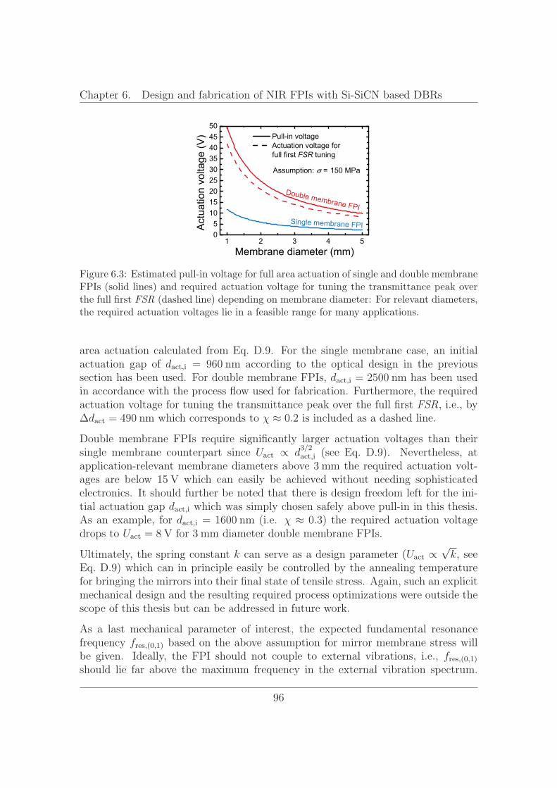
Chapter 6. Design and fabrication of NIR FPIs with Si-SiCN based DBRs
1 2 3 4 505101520253035404550
Double membrane FPIActuationvoltage(V)
Membrane diameter (mm)
Pull-in voltageActuation voltage forfull first FSR tuning
Single membrane FPI
Assumption: � = 150 MPa
Figure 6.3: Estimated pull-in voltage for full area actuation of single and double membraneFPIs (solid lines) and required actuation voltage for tuning the transmittance peak overthe full first FSR (dashed line) depending on membrane diameter: For relevant diameters,the required actuation voltages lie in a feasible range for many applications.
area actuation calculated from Eq. D.9. For the single membrane case, an initialactuation gap of d , = according to the optical design in the previoussection has been used. For double membrane FPIs, d , = has been usedin accordance with the process flow used for fabrication. Furthermore, the requiredactuation voltage for tuning the transmittance peak over the full first FSR, i.e., byΔd = which corresponds to χ ≈ 0.2 is included as a dashed line.
Double membrane FPIs require significantly larger actuation voltages than theirsingle membrane counterpart since U ∝ d
3/2, (see Eq. D.9). Nevertheless, at
application-relevant membrane diameters above the required actuation volt-ages are below which can easily be achieved without needing sophisticatedelectronics. It should further be noted that there is design freedom left for the ini-tial actuation gap d , which was simply chosen safely above pull-in in this thesis.As an example, for d , = (i.e. χ ≈ 0.3) the required actuation voltagedrops to U = for diameter double membrane FPIs.
Ultimately, the spring constant k can serve as a design parameter (U ∝√k, see
Eq. D.9) which can in principle easily be controlled by the annealing temperaturefor bringing the mirrors into their final state of tensile stress. Again, such an explicitmechanical design and the resulting required process optimizations were outside thescope of this thesis but can be addressed in future work.
As a last mechanical parameter of interest, the expected fundamental resonancefrequency f ,( , ) based on the above assumption for mirror membrane stress willbe given. Ideally, the FPI should not couple to external vibrations, i.e., f ,( , )
should lie far above the maximum frequency in the external vibration spectrum.
96
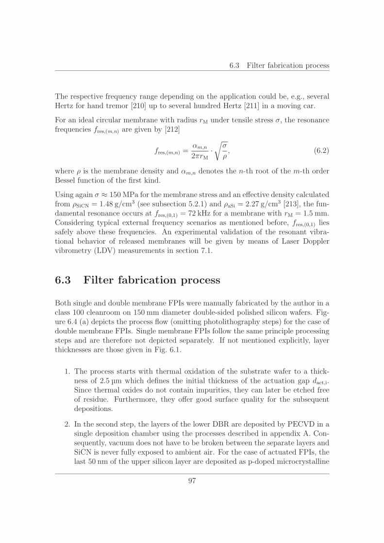
6.3 Filter fabrication process
The respective frequency range depending on the application could be, e.g., severalHertz for hand tremor [210] up to several hundred Hertz [211] in a moving car.
For an ideal circular membrane with radius r under tensile stress σ, the resonancefrequencies f ,(m,n) are given by [212]
fres,(m,n) =αm,n
2πr·√σ
ρ, (6.2)
where ρ is the membrane density and αm,n denotes the n-th root of the m-th orderBessel function of the first kind.
Using again σ ≈ for the membrane stress and an effective density calculatedfrom ρ = . / (see subsection 5.2.1) and ρ = . / [213], the fun-damental resonance occurs at f ,( , ) = for a membrane with r = . .Considering typical external frequency scenarios as mentioned before, f ,( , ) liessafely above these frequencies. An experimental validation of the resonant vibra-tional behavior of released membranes will be given by means of Laser Dopplervibrometry (LDV) measurements in section 7.1.
6.3 Filter fabrication process
Both single and double membrane FPIs were manually fabricated by the author in aclass 100 cleanroom on diameter double-sided polished silicon wafers. Fig-ure 6.4 (a) depicts the process flow (omitting photolithography steps) for the case ofdouble membrane FPIs. Single membrane FPIs follow the same principle processingsteps and are therefore not depicted separately. If not mentioned explicitly, layerthicknesses are those given in Fig. 6.1.
1. The process starts with thermal oxidation of the substrate wafer to a thick-ness of . which defines the initial thickness of the actuation gap d , .Since thermal oxides do not contain impurities, they can later be etched freeof residue. Furthermore, they offer good surface quality for the subsequentdepositions.
2. In the second step, the layers of the lower DBR are deposited by PECVD in asingle deposition chamber using the processes described in appendix A. Con-sequently, vacuum does not have to be broken between the separate layers andSiCN is never fully exposed to ambient air. For the case of actuated FPIs, thelast of the upper silicon layer are deposited as p-doped microcrystalline
97
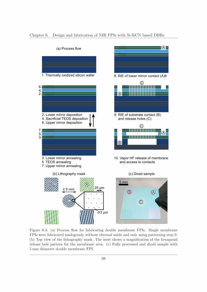
Chapter 6. Design and fabrication of NIR FPIs with Si-SiCN based DBRs
1. Thermally oxidized silicon wafer
2. Lower mirror deposition4. Sacrificial TEOS deposition6. Upper mirror deposition
3. Lower mirror annealing5. TEOS annealing7. Upper mirror annealing
8. RIE of lower mirror contact (A)8
9. RIE of substrate contact (B) and release holes (C)
10. Vapor HF release of membrane and access to contacts
2.4.6.
3.5.7.
A
B
C
A
B
C
A
C
B25 μm
3 μm
(a) Process flow
AB
C
5 mm
(b) Lithography mask (c) Diced sample
5 mm
Figure 6.4: (a) Process flow for fabricating double membrane FPIs. Single membraneFPIs were fabricated analogously without thermal oxide and only using patterning step 9.(b) Top view of the lithography mask. The inset shows a magnification of the hexagonalrelease hole pattern for the membrane area. (c) Fully processed and diced sample with
diameter double membrane FPI.
98
6.3 Filter fabrication process
silicon (μc-Si) in order to establish electrical contact later. This point will bediscussed in more detail further below.
3. Thermal annealing up to temperatures between ◦ and ◦ in nitrogenatmosphere is conducted as a means to establish tensile stress in the lowermirror. Even though the upper mirror will need thermal annealing as well,the lower mirror is annealed separately in order to reduce the risk of blisterformation (see subsection 6.4.1).
4. PECVD TEOS oxide, the thickness of which determines d , and therebyλ , , is deposited as the sacrificial oxide between the mirrors. Due tothe low deposition temperatures, PECVD TEOS oxide can contain significantamounts of impurities from the precursor gases [131]. Nevertheless, TEOS waschosen as the precursor instead of SiH4+N2O because the latter causes solidresidues of (NH4)2SiF6 after HF etching due to residual nitrogen [131].
5. Residual amounts of carbon in PECVD TEOS oxide can be significantly re-duced by annealing [131]. Therefore, a second annealing is performed in orderto reduce solid residues after the release process. Since very high stress levelsfor the lower mirror are undesired because of the resulting required actuationvoltages, annealing temperature is restricted to the same regime as in the thirdstep.
6. The upper mirror is deposited analogously to the lower mirror
7. and subsequently annealed.
8. Square openings (see Fig. 6.4 (b) in green, marked as ”A”) are patterned intothe upper mirror using standard photolithography with positive tone resist,reactive ion etching (RIE)6 and finally removal of the resist in an oxygenplasma. After HF etching in step 10, the conductive μc-Si layer of the lowermirror will be accessible for contacting through these openings.
9. A second lithography step is used to define further square openings in theremaining corners of the chip as well as release hole openings in the membranearea (Fig. 6.4 (b) in blue, marked as ”B” and ”C”). The release holes (mostly
in diameter; other diameters have been used in design variants) arearranged in a circularly-cut hexagonal pattern with lattice constant.In this configuration, the release holes account for . of the total mirrorarea so that their detrimental influence on filter performance is small. Afterlithography, anisotropic RIE is again used to etch through both mirrors and the
6RIE was actually performed on the very first machine at which deep RIE of silicon (also knownas the Bosch process) had been developed in 1992 [214].
99
Chapter 6. Design and fabrication of NIR FPIs with Si-SiCN based DBRs
intermediate sacrificial oxide. Thereby, circular mirror regions with diametersup to are defined.
10. After dicing, HF vapor release is performed with individual chips. Etchingreleases both membranes and removes the oxide in the contact openings (A,B)so that both, lower mirror and substrate wafer are accessible for contacting.Further details on the etch process can be found in subsection 6.4.3 and 6.4.4.
For fabrication of single membrane FPIs, thermal oxidation in the initial step isskipped, the lower mirror is deposited with an additional SiCN layer as discussed insection 6.1 and only patterning step 9 is needed to define release holes in the uppermirror and contact openings to the lower mirror.
In order to be able to actuate the released FPIs, at least one layer per mirror hasto be electrically conductive so that it can be used as an actuation electrode. Here,one of the silicon layers in the mirrors takes that role. Classically, doping witheither group III or V elements is used to increase p- or n- conductivity of crystallineor polycrystalline silicon, respectively. Doping of amorphous hydrogenated silicon ispossible as well, despite doping efficiency being low because the amorphous structureforces only few dopant atoms into four-fold coordinated bonds and many excesscarriers become trapped in deep defects [215]. However, for small thicknesses ofdoped a-Si below approximately , specific conductance drops by orders ofmagnitude [216–218] presumably due to a depleted space-charge region close to oneof the interfaces. Therefore, no conductive a-Si layers could be deposited in thisthesis with the silicon thickness restricted to be in the DBR.
If SiH4 is strongly diluted in H2 during PECVD, a transition to μc-Si growth oc-curs because hydrogen radicals preferentially etch weakly coordinated silicon [215].The electronic properties of this μc-Si lie between those of a-Si and crystalline sili-con, i.e., it can be doped more effectively [215] enabling high conductivity even atsmall thicknesses. However, growth of crystallites can lead to voids in the mate-rial [215], effectively reducing the refractive index and increasing surface roughness.Therefore, this thesis aimed at conductive μc-Si with minimal thickness. It wasfound that of boron-doped μc-Si provided sufficient conductivity to be usedas an electrode. The microcrystalline phase could be evidenced by the presence ofboth the crystalline and the amorphous silicon peak in Raman spectra (not shownhere) [219]. Accordingly, growth of the top layer a-Si in both mirrors was stoppedafter and the remaining film was grown as boron-doped μc-Si in the samedeposition chamber.
This configuration has an impact on the travel range. As the conducting layersare the topmost silicon layers of both mirrors, the underlying Si/SiCN layers of the
100
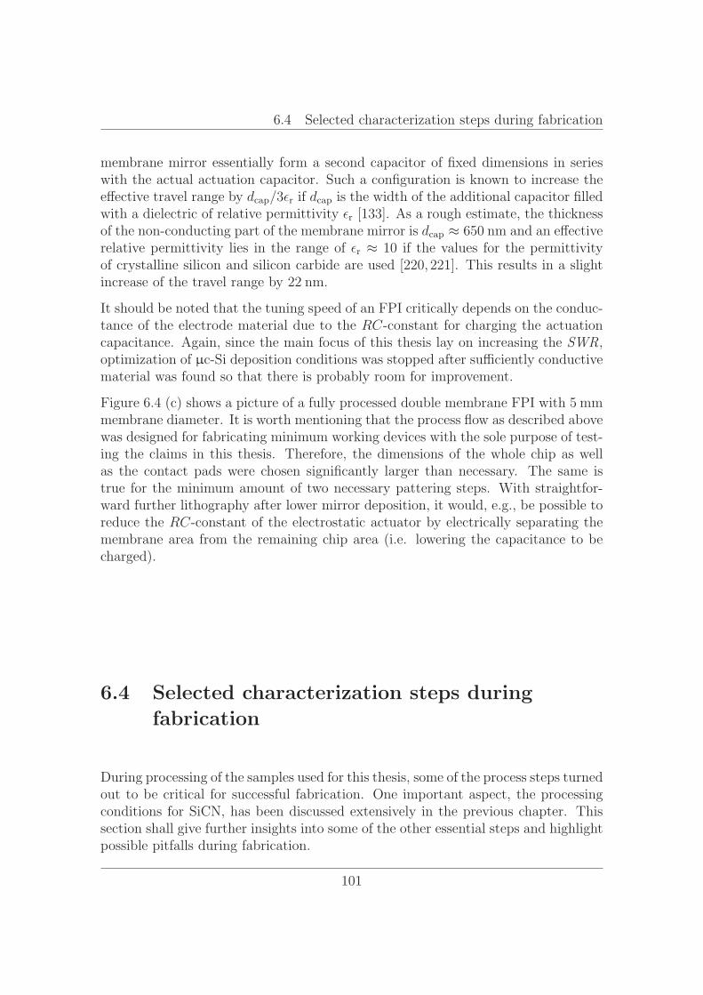
6.4 Selected characterization steps during fabrication
membrane mirror essentially form a second capacitor of fixed dimensions in serieswith the actual actuation capacitor. Such a configuration is known to increase theeffective travel range by d /3ε if d is the width of the additional capacitor filledwith a dielectric of relative permittivity ε [133]. As a rough estimate, the thicknessof the non-conducting part of the membrane mirror is d ≈ and an effectiverelative permittivity lies in the range of ε ≈ 10 if the values for the permittivityof crystalline silicon and silicon carbide are used [220, 221]. This results in a slightincrease of the travel range by .
It should be noted that the tuning speed of an FPI critically depends on the conduc-tance of the electrode material due to the RC-constant for charging the actuationcapacitance. Again, since the main focus of this thesis lay on increasing the SWR,optimization of μc-Si deposition conditions was stopped after sufficiently conductivematerial was found so that there is probably room for improvement.
Figure 6.4 (c) shows a picture of a fully processed double membrane FPI withmembrane diameter. It is worth mentioning that the process flow as described abovewas designed for fabricating minimum working devices with the sole purpose of test-ing the claims in this thesis. Therefore, the dimensions of the whole chip as wellas the contact pads were chosen significantly larger than necessary. The same istrue for the minimum amount of two necessary pattering steps. With straightfor-ward further lithography after lower mirror deposition, it would, e.g., be possible toreduce the RC-constant of the electrostatic actuator by electrically separating themembrane area from the remaining chip area (i.e. lowering the capacitance to becharged).
6.4 Selected characterization steps during
fabrication
During processing of the samples used for this thesis, some of the process steps turnedout to be critical for successful fabrication. One important aspect, the processingconditions for SiCN, has been discussed extensively in the previous chapter. Thissection shall give further insights into some of the other essential steps and highlightpossible pitfalls during fabrication.
101
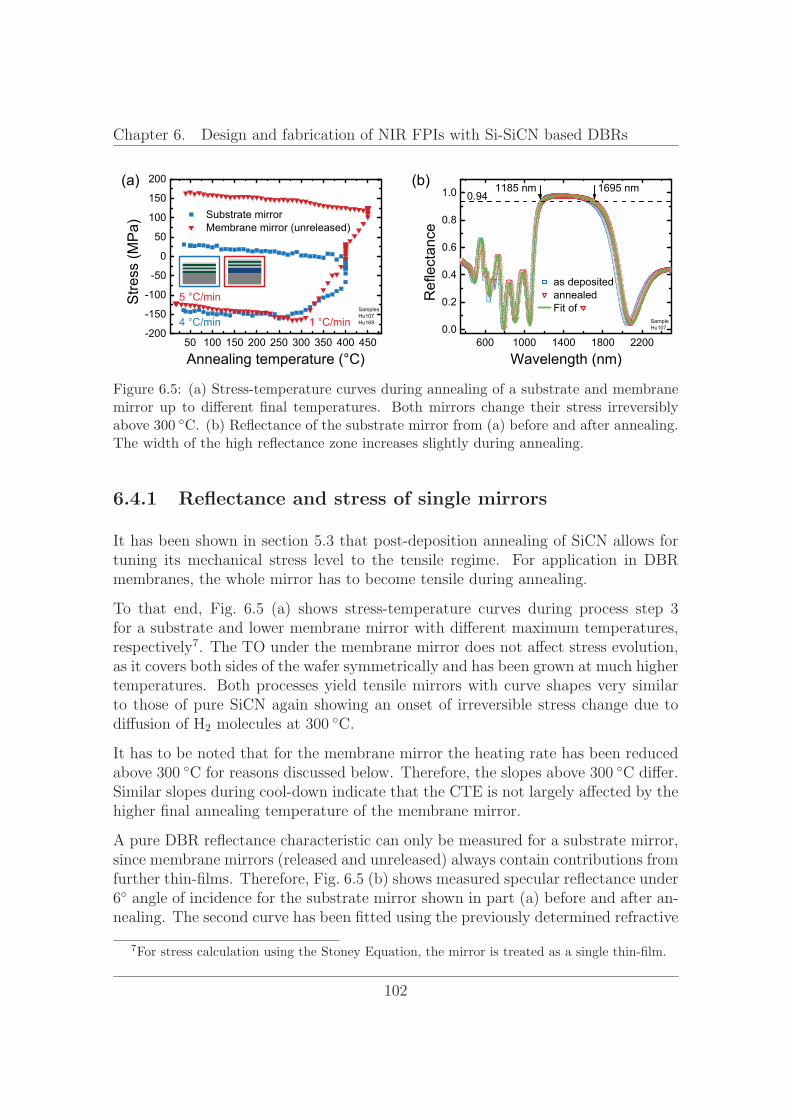
Chapter 6. Design and fabrication of NIR FPIs with Si-SiCN based DBRs
50 100 150 200 250 300 350 400 450-200
-150
-100
-50
0
50
100
150
200
1 °C/min
Stress(MPa)
Annealing temperature (°C)
Substrate mirrorMembrane mirror (unreleased)
SamplesHu107Hu169
5 °C/min
4 °C/min
(a)
600 1000 1400 1800 22000.0
0.2
0.4
0.6
0.8
1.0
Reflectance
Wavelength (nm)
as depositedannealedFit of
SampleHu107
1185 nm 1695 nm0.94
(b)
Figure 6.5: (a) Stress-temperature curves during annealing of a substrate and membranemirror up to different final temperatures. Both mirrors change their stress irreversiblyabove ◦ . (b) Reflectance of the substrate mirror from (a) before and after annealing.The width of the high reflectance zone increases slightly during annealing.
6.4.1 Reflectance and stress of single mirrors
It has been shown in section 5.3 that post-deposition annealing of SiCN allows fortuning its mechanical stress level to the tensile regime. For application in DBRmembranes, the whole mirror has to become tensile during annealing.
To that end, Fig. 6.5 (a) shows stress-temperature curves during process step 3for a substrate and lower membrane mirror with different maximum temperatures,respectively7. The TO under the membrane mirror does not affect stress evolution,as it covers both sides of the wafer symmetrically and has been grown at much highertemperatures. Both processes yield tensile mirrors with curve shapes very similarto those of pure SiCN again showing an onset of irreversible stress change due todiffusion of H2 molecules at ◦ .
It has to be noted that for the membrane mirror the heating rate has been reducedabove ◦ for reasons discussed below. Therefore, the slopes above ◦ differ.Similar slopes during cool-down indicate that the CTE is not largely affected by thehigher final annealing temperature of the membrane mirror.
A pure DBR reflectance characteristic can only be measured for a substrate mirror,since membrane mirrors (released and unreleased) always contain contributions fromfurther thin-films. Therefore, Fig. 6.5 (b) shows measured specular reflectance under◦ angle of incidence for the substrate mirror shown in part (a) before and after an-nealing. The second curve has been fitted using the previously determined refractive
7For stress calculation using the Stoney Equation, the mirror is treated as a single thin-film.
102
6.4 Selected characterization steps during fabrication
500 μmSampleHu097
(a)
0.0 0.5 1.0 1.50
5
10
15
Height(μm)
Distance (mm)
SampleHu098
(b)
Figure 6.6: Blister formation during annealing of mirrors. (a) Microscope image of blistersin a lower membrane mirror at the edge of the wafer after annealing. (b) Profilometer scanover a mirror blister.
index values for SiCN and a-Si from ellipsometry by only varying the thicknessesresulting in excellent agreement over the whole spectral range.
The reflectance curves show the desired plateau with its maximum of 0.981 (de-signed: 0.976) reached at around after annealing. The dashed line at 0.94reflectance intersects at and indicating that the mirror indeedshows high reflectance over the major part of the SWR.
6.4.2 Mirror blistering during annealing
As discussed in section 5.3, single layers of SiCN can be annealed up to the pointwhere they delaminate due to excessive tensile stress. This happens far above thedesired stress values for a FPI membrane DBR. In the DBR, however, SiCN layersare capped by dense layers of amorphous silicon8. When hydrogen molecules start todiffuse in SiCN above ◦ , they cannot easily penetrate a-Si [222]. This can leadto the formation of blisters or, in case pressure inside the bubbles exceeds a criticalvalue, also their rupture. Similar observations have been reported for hydrogenatedamorphous silicon, where blisters started to form at ◦ [223]. The microscopeimage on the left side of Fig. 6.6 and the profilometer scan over such a blister onthe right side reveal that these blisters can reach diameters in the millimeter rangeand heights of several micrometers.
8The deposition conditions for a-Si are chosen such as to maximize its refractive index. The finalrefractive index in the NIR is indeed around 3.5, i.e., close to that of crystalline silicon indicatinga dense layer.
103
Chapter 6. Design and fabrication of NIR FPIs with Si-SiCN based DBRs
Formation of such blisters can be reduced by reducing the heating rate above ◦ ,when hydrogen effusion starts. However, especially after the last mirror deposition,blister formation could never fully be prevented. Blisters are especially detrimentalas a source of particle contamination after rupture. Further process optimization inthe annealing step is necessary to achieve blister-free samples reliably.
6.4.3 Mirror layer delamination during prolongedHF etching
Gas phase HF etching of SiO2 is governed by the following overall reaction equation[224]:
( ) + ( )( )−−−−−→ ↑ + ( ) (6.3)
Water acts as a catalyst because it promotes ionization of adsorbed HF according to2HF+H2O −−→ HF2
– +H3O+ to form the actual reactive species. Therefore, water
is needed to initiate etching, e.g., by providing it externally. However, water is alsocreated by the reaction and thus accelerates the etch process if not transported awayfrom the etch front. Furthermore, in the case of excess water being created duringunderetching of microstructures, stiction can occur due to capillary forces similarlyto stiction during drying in a wet etch process [225, 226]. Consequently, high etchrates corresponding to large amounts of water between substrate and released partincrease the risk of stiction.
Control of the etch rate is possible via the residence time of adsorbed water at theetch front, which can be reduced either by reducing process pressure or increasingtemperature (apart from reducing the external water supply rate). The safest ap-proach to prevent stiction is therefore to etch at low pressure and low water supplyrate as it was the case for the ”slow” process in section 5.4. It was shown that aSiCN thin-film etches at only a few nanometers per hour under these conditions.Since HF can attack SiCN only at the edges of the release holes this etch rate isnegligible even for long processes.
However, after HF etching for in order to release single membrane FPIs witha ”slow” process, mirror membranes were released but showed an obvious attackvisible by a change of the interference color. In order to investigate the cause for thisattack, a substrate mirror was deposited and subsequently structured with releaseholes (even though no sacrificial oxide to be released was present). Figure 6.7 (upperpart) shows SEM cross sections of a substrate mirror within the structured area asit was deposited (a) and after a ”slow” HF process (b). It can be seen that thebulk of SiCN stays indeed intact but delamination occurs at some of the Si/SiCN
104
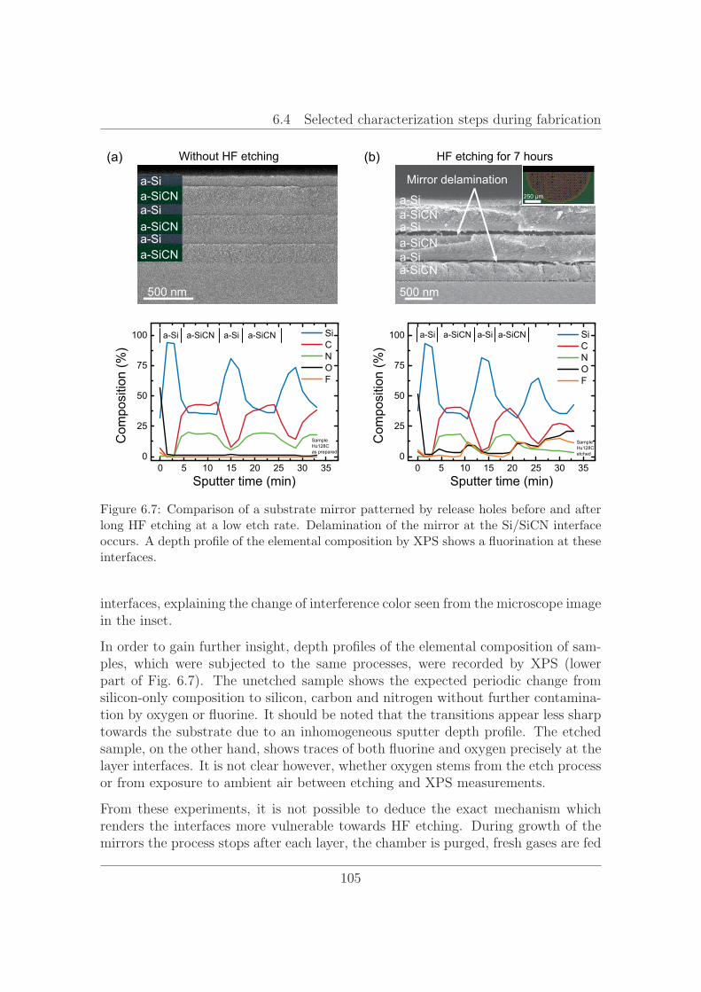
6.4 Selected characterization steps during fabrication
500 nm
Without HF etching
a-Si
a-Si
a-Si
a-SiCN
a-SiCN
a-SiCN
(a)
500 nm
Mirror delamination
HF etching for 7 hours
a-Si
a-Si
a-Si
a-SiCN
a-SiCN
a-SiCN
250 μm
(b)
0 5 10 15 20 25 30 350
25
50
75
100
SampleHu128Cas prepared
a-Si a-SiCNa-SiCN
Composition(%)
Sputter time (min)
SiCNOF
a-Si
0 5 10 15 20 25 30 350
25
50
75
100
Composition(%)
Sputter time (min)
SiCNOF
SampleHu128Cetched
a-Si a-SiCN a-Si a-SiCN
Figure 6.7: Comparison of a substrate mirror patterned by release holes before and afterlong HF etching at a low etch rate. Delamination of the mirror at the Si/SiCN interfaceoccurs. A depth profile of the elemental composition by XPS shows a fluorination at theseinterfaces.
interfaces, explaining the change of interference color seen from the microscope imagein the inset.
In order to gain further insight, depth profiles of the elemental composition of sam-ples, which were subjected to the same processes, were recorded by XPS (lowerpart of Fig. 6.7). The unetched sample shows the expected periodic change fromsilicon-only composition to silicon, carbon and nitrogen without further contamina-tion by oxygen or fluorine. It should be noted that the transitions appear less sharptowards the substrate due to an inhomogeneous sputter depth profile. The etchedsample, on the other hand, shows traces of both fluorine and oxygen precisely at thelayer interfaces. It is not clear however, whether oxygen stems from the etch processor from exposure to ambient air between etching and XPS measurements.
From these experiments, it is not possible to deduce the exact mechanism whichrenders the interfaces more vulnerable towards HF etching. During growth of themirrors the process stops after each layer, the chamber is purged, fresh gases are fed
105
Chapter 6. Design and fabrication of NIR FPIs with Si-SiCN based DBRs
into the chamber and the plasma is reignited. This might lead to a different growthof the initial layer. If, e.g., the density of SiCN is reduced at the interfaces, HF,being an extremely mobile gas due to the small size of the molecules, could be ableto penetrate SiCN and attack at the interfaces only.
However, the results illustrate that simply reducing the etch speed for the wholeprocess to prevent stiction is not a useful release strategy so that a modified processdescribed in the next subsection has to be used.
6.4.4 Stiction-free release of first order FPIs at largemembrane diameters
Stiction occurs during vapor HF etching if a water film forms between substrateand movable part and the attractive capillary force of the water meniscus exceedsthe restoring force of the released part upon deflection. For a clamped membraneof thickness d and stress σ, the Hookean restoring force at a deflection Δd isK = Δd · 4πd σ (see Eq. 6.1). On the other hand, capillary force K betweentwo FPI mirrors scales as K = p πr2 ∝ r2 /d , where p is capillarypressure [227, 228]. Consequently, large-area, thin membranes at small separationsare especially prone to stiction. In particular, this is the case for double membraneFPIs where two large-area deflectable membranes are present which are separatedby a smaller initial gap than in their single membrane FPI counterpart.
It has been shown in the previous subsection that very long etch times at low speedare not feasible due to mirror delamination. However, by choosing different etchrates during the process, the problem can be circumvented. Figure 6.8 illustratesthe process at its different stages. The top row shows schematic cross sections, themiddle row infrared microscope top views and the bottom row a measured SiF4 ab-sorption line signal from the HF chamber’s end point detection which is an indicatorfor the current etch speed.
Starting from the patterned wafer (a), etching starts isotropically in the sacrificialoxides around the release holes. Additionally, TEOS oxide between the mirrorsetches considerably faster than dense TO under the mirrors [131]. Since the releaseholes are arranged periodically in equilateral triangles, isotropic etching results increation of TEOS support columns at the triangle center points (b). Up to thismoment, stiction does not occur because of the regular support so that etching canbe done at a high speed. For instance, the undercut in the infrared microscope image(b) was achieved in corresponding to a high etch rate of roughly . / .
106
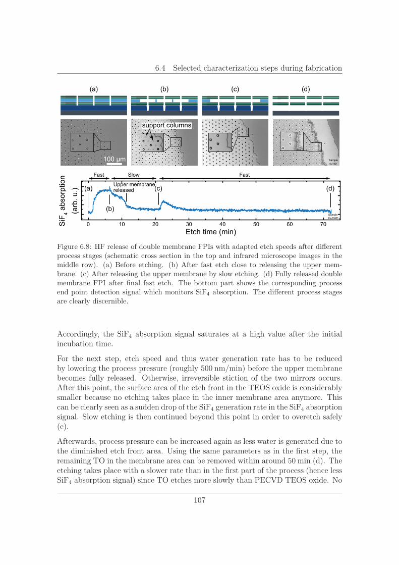
6.4 Selected characterization steps during fabrication
(a) (b) (c) (d)
0 10 20 30 40 50 60 70SiF
4 abs
orpt
ion
(arb
. u.)
Etch time (min)
SampleHu192D
(a)
(b)
(c) (d)Upper membranereleased
Fast Slow Fast
100 μm
support columns
SampleHu192
Figure 6.8: HF release of double membrane FPIs with adapted etch speeds after differentprocess stages (schematic cross section in the top and infrared microscope images in themiddle row). (a) Before etching. (b) After fast etch close to releasing the upper mem-brane. (c) After releasing the upper membrane by slow etching. (d) Fully released doublemembrane FPI after final fast etch. The bottom part shows the corresponding processend point detection signal which monitors SiF4 absorption. The different process stagesare clearly discernible.
Accordingly, the SiF4 absorption signal saturates at a high value after the initialincubation time.
For the next step, etch speed and thus water generation rate has to be reducedby lowering the process pressure (roughly / ) before the upper membranebecomes fully released. Otherwise, irreversible stiction of the two mirrors occurs.After this point, the surface area of the etch front in the TEOS oxide is considerablysmaller because no etching takes place in the inner membrane area anymore. Thiscan be clearly seen as a sudden drop of the SiF4 generation rate in the SiF4 absorptionsignal. Slow etching is then continued beyond this point in order to overetch safely(c).
Afterwards, process pressure can be increased again as less water is generated due tothe diminished etch front area. Using the same parameters as in the first step, theremaining TO in the membrane area can be removed within around (d). Theetching takes place with a slower rate than in the first part of the process (hence lessSiF4 absorption signal) since TO etches more slowly than PECVD TEOS oxide. No
107
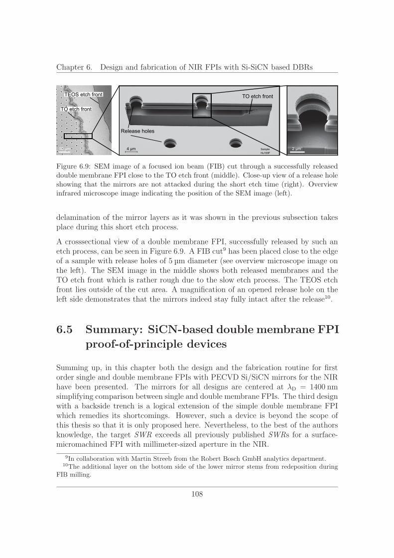
Chapter 6. Design and fabrication of NIR FPIs with Si-SiCN based DBRs
4 μm 2 μm
TO etch front
Release holes
SampleHu169F
50 μm
TO etch front
TEOS etch front
Figure 6.9: SEM image of a focused ion beam (FIB) cut through a successfully releaseddouble membrane FPI close to the TO etch front (middle). Close-up view of a release holeshowing that the mirrors are not attacked during the short etch time (right). Overviewinfrared microscope image indicating the position of the SEM image (left).
delamination of the mirror layers as it was shown in the previous subsection takesplace during this short etch process.
A crosssectional view of a double membrane FPI, successfully released by such anetch process, can be seen in Figure 6.9. A FIB cut9 has been placed close to the edgeof a sample with release holes of diameter (see overview microscope image onthe left). The SEM image in the middle shows both released membranes and theTO etch front which is rather rough due to the slow etch process. The TEOS etchfront lies outside of the cut area. A magnification of an opened release hole on theleft side demonstrates that the mirrors indeed stay fully intact after the release10.
6.5 Summary: SiCN-based double membrane FPI
proof-of-principle devices
Summing up, in this chapter both the design and the fabrication routine for firstorder single and double membrane FPIs with PECVD Si/SiCN mirrors for the NIRhave been presented. The mirrors for all designs are centered at λ =simplifying comparison between single and double membrane FPIs. The third designwith a backside trench is a logical extension of the simple double membrane FPIwhich remedies its shortcomings. However, such a device is beyond the scope ofthis thesis so that it is only proposed here. Nevertheless, to the best of the authorsknowledge, the target SWR exceeds all previously published SWRs for a surface-micromachined FPI with millimeter-sized aperture in the NIR.
9In collaboration with Martin Streeb from the Robert Bosch GmbH analytics department.10The additional layer on the bottom side of the lower mirror stems from redeposition during
FIB milling.
108
6.5 Summary: SiCN-based double membrane FPI proof-of-principle devices
Though not designed explicitly, the mechanical behavior in terms of membrane shapeduring deflection, actuation voltage and resonance frequency has been predictedbased on an analytical model for the actuator.
FPIs fabricated by the presented process flow are fully functional proof-of-principledevices in the sense that all advantages of double membrane FPIs discussed insection 4.3 with respect to their single membrane counterpart can be tested. Fur-thermore, since the two designs are actually equal (apart from the configuration ofthe lower mirror), all differences in performance in the next two chapters can befully attributed to the double membrane approach.
Finally, it has been shown that proper stress control by means of annealing is pos-sible without negatively affecting mirror reflectance, even though careful annealingis required due to a risk of mirror blistering. Additionally, the release step is chal-lenging since etching has to be fast enough to prevent mirror delamination whilesimultaneously being slow enough to avoid stiction.
109

Chapter 6. Design and fabrication of NIR FPIs with Si-SiCN based DBRs
110
Chapter 7
Static Fabry-Perot interferometerswith membrane mirrors
When no actuation voltage U is applied, released MEMS FPIs fabricated accordingto section 6.3 function as static filters. Their transmittance wavelength then dependson the initial optical gap d , which is determined by the thickness of the intermirrorTEOS oxide. Several aspects about the filter performance such as the improvedmirror parallelism in double membrane FPIs claimed in section 4.3 can therefore betested with static devices as well, avoiding possible additional non-idealities due toactuation.
To that end, initial characterization was performed on a series of dedicated staticFPIs. In contrast to the TEOS oxide thickness d for tunable FPIs given inthe previous chapter, d was chosen such that the first order transmittance peaklies at roughly the design wavelength of the DBR, i.e., d , = . This offersthe advantage of maximum sensitivity towards gap inhomogeneities due to highmirror reflectance and resulting sharp transmission peaks. In consequence, onlynon-conductive amorphous silicon was used during fabrication instead of depositingthe last of every mirror in the microcrystalline phase. Accordingly, possibleabsorption losses due to doping are reduced and stress gradients in the mirrors dueto a broken symmetry are prevented.
The chapter starts by examining the prestressed top mirror membrane. First, thefrequency spectrum for vibrational excitations of the mirror membrane is analyzedin section 7.1. This allows the residual tensile stress level to be extracted from theeigenmode resonance frequencies. Next, measurements of the top membrane mirror’ssurface profiles are presented in section 7.2 in order to demonstrate the achievableflatness over large areas.
111
Chapter 7. Static Fabry-Perot interferometers with membrane mirrors
The remaining chapter focuses on optical characterization by transmittance mea-surements. To that end, a spatially-resolved transmittance setup is introduced insection 7.3 and its capability to measure spatial maps of d , is presented. Thechapter ends with a detailed comparison between single and double membrane FPIsin terms of their optical gap homogeneity in section 7.4. Thereby, the claims fromsection 4.3 regarding a higher degree of parallelism between the mirrors in doublemembrane FPIs can be tested.
Parts of the results of this chapter have been published in [18].
7.1 Stress determination from the vibrational
excitation spectrum of released membranes
In section 6.2, an estimate for the fundamental resonance frequency f ,( , ) of areleased membrane has been given. Here, the vibrational spectrum of such a re-leased membrane will be examined in order to verify that resonances indeed lie farabove natural external frequencies. Furthermore, the frequency spectrum will allowmembrane stress to be derived experimentally.
To that end, the vibrational frequency spectrum of an FPI with diameter hasbeen recorded for its out-of-plane movement over a grid of coordinates at variousbackground pressures using a Polytec MSA-100-3D LDV (see Appendix A). It isshown in Fig. 7.1 for frequencies up to .
Upon excitation, the frequency spectrum exhibits a series of resonance peaks cor-responding to the eigenmodes of the structure. The latter can be matched to theeigenmodes of a circular membrane which are excited depending on their modalparticipation factor. The theoretical spatial profile u(r, ϕ)(m,n) of the eigenmodes inpolar coordinates r, ϕ is given by [212]
u(r, ϕ)(m,n) = Jm
(αm,n ·
r
r
)· (mϕ) , (7.1)
where Jm denotes the m-th order Bessel function of the first kind and αm,n is itsn-th root. In other words, m describes the number of nodal diameters of u(r, ϕ)(m,n)
whereas n counts the number of nodal circles. Every theoretically expected reso-nance in this frequency range up to the (0, 3) mode could be observed. Their spatial(theoretical) profile is depicted in Fig. 7.1 for reference.
It is worth to note that modes with m > 0 are degenerate for an ideal membrane.In Fig. 7.1, degeneracy is lifted and the respective resonance peaks are split due
112
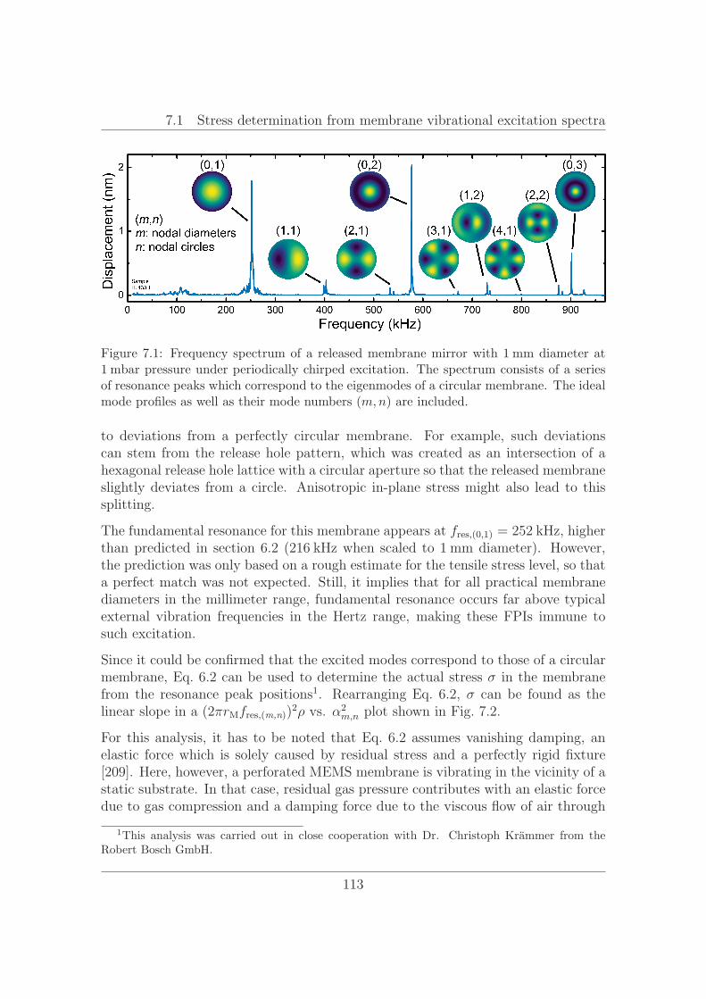
7.1 Stress determination from membrane vibrational excitation spectra
Figure 7.1: Frequency spectrum of a released membrane mirror with diameter atpressure under periodically chirped excitation. The spectrum consists of a series
of resonance peaks which correspond to the eigenmodes of a circular membrane. The idealmode profiles as well as their mode numbers (m,n) are included.
to deviations from a perfectly circular membrane. For example, such deviationscan stem from the release hole pattern, which was created as an intersection of ahexagonal release hole lattice with a circular aperture so that the released membraneslightly deviates from a circle. Anisotropic in-plane stress might also lead to thissplitting.
The fundamental resonance for this membrane appears at f ,( , ) = , higherthan predicted in section 6.2 ( when scaled to diameter). However,the prediction was only based on a rough estimate for the tensile stress level, so thata perfect match was not expected. Still, it implies that for all practical membranediameters in the millimeter range, fundamental resonance occurs far above typicalexternal vibration frequencies in the Hertz range, making these FPIs immune tosuch excitation.
Since it could be confirmed that the excited modes correspond to those of a circularmembrane, Eq. 6.2 can be used to determine the actual stress σ in the membranefrom the resonance peak positions1. Rearranging Eq. 6.2, σ can be found as thelinear slope in a (2πr f ,(m,n))
2ρ vs. α2m,n plot shown in Fig. 7.2.
For this analysis, it has to be noted that Eq. 6.2 assumes vanishing damping, anelastic force which is solely caused by residual stress and a perfectly rigid fixture[209]. Here, however, a perforated MEMS membrane is vibrating in the vicinity of astatic substrate. In that case, residual gas pressure contributes with an elastic forcedue to gas compression and a damping force due to the viscous flow of air through
1This analysis was carried out in close cooperation with Dr. Christoph Krammer from theRobert Bosch GmbH.
113
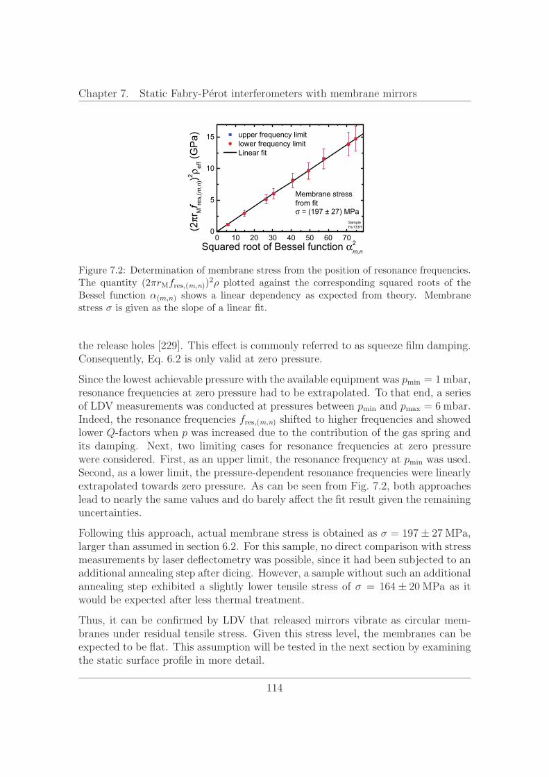
Chapter 7. Static Fabry-Perot interferometers with membrane mirrors
0 10 20 30 40 50 60 700
5
10
15
(2πrMf res,(m,n))2
ρ eff(GPa)
Squared root of Bessel function α2m,n
upper frequency limitlower frequency limitLinear fit
Membrane stressfrom fitσ = (197 ± 27) MPa
SampleHu133H
Figure 7.2: Determination of membrane stress from the position of resonance frequencies.The quantity (2πr f ,(m,n))
2ρ plotted against the corresponding squared roots of theBessel function α(m,n) shows a linear dependency as expected from theory. Membranestress σ is given as the slope of a linear fit.
the release holes [229]. This effect is commonly referred to as squeeze film damping.Consequently, Eq. 6.2 is only valid at zero pressure.
Since the lowest achievable pressure with the available equipment was p = ,resonance frequencies at zero pressure had to be extrapolated. To that end, a seriesof LDV measurements was conducted at pressures between p and p = .Indeed, the resonance frequencies f ,(m,n) shifted to higher frequencies and showedlower Q-factors when p was increased due to the contribution of the gas spring andits damping. Next, two limiting cases for resonance frequencies at zero pressurewere considered. First, as an upper limit, the resonance frequency at p was used.Second, as a lower limit, the pressure-dependent resonance frequencies were linearlyextrapolated towards zero pressure. As can be seen from Fig. 7.2, both approacheslead to nearly the same values and do barely affect the fit result given the remaininguncertainties.
Following this approach, actual membrane stress is obtained as σ = ± ,larger than assumed in section 6.2. For this sample, no direct comparison with stressmeasurements by laser deflectometry was possible, since it had been subjected to anadditional annealing step after dicing. However, a sample without such an additionalannealing step exhibited a slightly lower tensile stress of σ = ± as itwould be expected after less thermal treatment.
Thus, it can be confirmed by LDV that released mirrors vibrate as circular mem-branes under residual tensile stress. Given this stress level, the membranes can beexpected to be flat. This assumption will be tested in the next section by examiningthe static surface profile in more detail.
114
7.2 Surface flatness of the upper membrane mirror
7.2 Surface flatness of the upper membrane
mirror
As shown in the previous section, tensile stress has successfully been established inthe mirror membranes by thermal annealing. Now, mechanical stylus profilometryand white light interferometry (WLI) will be used to quantify the resulting surfaceflatness. To that end, the two methods are first compared when applied to a flatreleased membrane in subsection 7.2.1. Subsequently, a membrane in the presence ofanisotropic stress will be analyzed in subsection 7.2.2 in order to test the respectivepredictions for the surface profile from subsection 4.2.3.
7.2.1 Comparison of profilometric and white lightinterferometric surface profile measurements
In previous studies, two methods have been employed to probe surface flatness ofreleased membranes: Mechanical stylus profilometry [44, 91, 230] and optical pro-filometry methods [46,115] such as WLI [83,101,231,232].
Stylus profilometry offers fast linescans with both high lateral and vertical resolution.However, a released membrane is deflected when a force is applied by the stylus.Therefore, an approximation of the true surface profile has been gained from alinear extrapolation of the deflection caused by a series of low stylus forces [44].
WLI provides contact-free surface maps with high vertical resolution. When mea-suring a thin-film stack, all films contribute to the interference signal on the camerawhich leads to a modification of the interferogram [233]. Therefore, care has tobe taken at the edges of released membranes when the underlying thin-film stackchanges abruptly.
Since both a stylus profilometer and a white light interferometer were available forthis thesis, their suitability for surface profiling of released DBR membranes can becompared. To that end, Fig. 7.3 shows (a) a series of stylus profilometer scans and(b) a WLI measurement of the surface of a released single membrane FPI withdiameter.
As expected, the membrane is increasingly deflected for increasing stylus forces. Thelargest available stylus force of suffices to locally deflect the membrane downto the substrate mirror as evidenced from the flat plateau (indicated by a dashedline). The displacement in the middle is slightly larger than the ellipsometrically
115
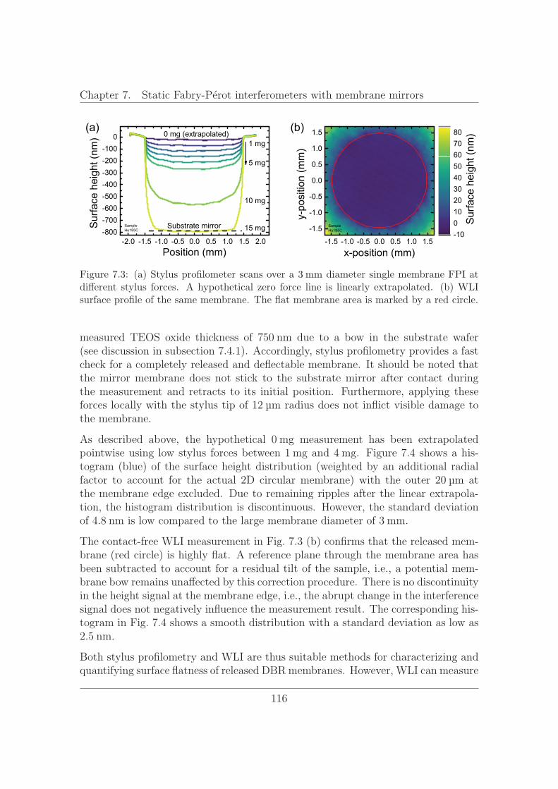
Chapter 7. Static Fabry-Perot interferometers with membrane mirrors
-2.0 -1.5 -1.0 -0.5 0.0 0.5 1.0 1.5 2.0-800-700-600-500-400-300-200-1000
15 mg
5 mg
Surfaceheight(nm)
Position (mm)
SampleHu185C
0 mg (extrapolated)1 mg
10 mg
Substrate mirror
(a)
-1.5 -1.0 -0.5 0.0 0.5 1.0 1.5
-1.5
-1.0
-0.5
0.0
0.5
1.0
1.5
Sur
face
hei
ght (
nm)
y-po
sitio
n (m
m)
x-position (mm)
-1001020304050607080
SampleHu185C
(b)
Figure 7.3: (a) Stylus profilometer scans over a diameter single membrane FPI atdifferent stylus forces. A hypothetical zero force line is linearly extrapolated. (b) WLIsurface profile of the same membrane. The flat membrane area is marked by a red circle.
measured TEOS oxide thickness of due to a bow in the substrate wafer(see discussion in subsection 7.4.1). Accordingly, stylus profilometry provides a fastcheck for a completely released and deflectable membrane. It should be noted thatthe mirror membrane does not stick to the substrate mirror after contact duringthe measurement and retracts to its initial position. Furthermore, applying theseforces locally with the stylus tip of radius does not inflict visible damage tothe membrane.
As described above, the hypothetical measurement has been extrapolatedpointwise using low stylus forces between and . Figure 7.4 shows a his-togram (blue) of the surface height distribution (weighted by an additional radialfactor to account for the actual 2D circular membrane) with the outer atthe membrane edge excluded. Due to remaining ripples after the linear extrapola-tion, the histogram distribution is discontinuous. However, the standard deviationof . is low compared to the large membrane diameter of .
The contact-free WLI measurement in Fig. 7.3 (b) confirms that the released mem-brane (red circle) is highly flat. A reference plane through the membrane area hasbeen subtracted to account for a residual tilt of the sample, i.e., a potential mem-brane bow remains unaffected by this correction procedure. There is no discontinuityin the height signal at the membrane edge, i.e., the abrupt change in the interferencesignal does not negatively influence the measurement result. The corresponding his-togram in Fig. 7.4 shows a smooth distribution with a standard deviation as low as. .
Both stylus profilometry and WLI are thus suitable methods for characterizing andquantifying surface flatness of released DBRmembranes. However, WLI can measure
116
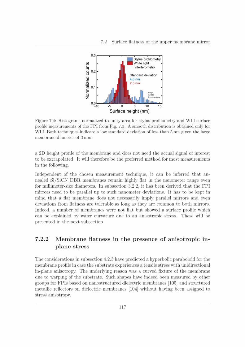
7.2 Surface flatness of the upper membrane mirror
-10 -5 0 5 10 150.0
0.1
0.2
0.3
Normalizedcounts
Surface height (nm)
Stylus profilometryWhite lightinterferometry
SampleHu185C3 mm membrane
Standard deviation4.8 nm2.5 nm
Figure 7.4: Histograms normalized to unity area for stylus profilometry and WLI surfaceprofile measurements of the FPI from Fig. 7.3. A smooth distribution is obtained only forWLI. Both techniques indicate a low standard deviation of less than given the largemembrane diameter of .
a 2D height profile of the membrane and does not need the actual signal of interestto be extrapolated. It will therefore be the preferred method for most measurementsin the following.
Independent of the chosen measurement technique, it can be inferred that an-nealed Si/SiCN DBR membranes remain highly flat in the nanometer range evenfor millimeter-size diameters. In subsection 3.2.2, it has been derived that the FPImirrors need to be parallel up to such nanometer deviations. It has to be kept inmind that a flat membrane does not necessarily imply parallel mirrors and evendeviations from flatness are tolerable as long as they are common to both mirrors.Indeed, a number of membranes were not flat but showed a surface profile whichcan be explained by wafer curvature due to an anisotropic stress. These will bepresented in the next subsection.
7.2.2 Membrane flatness in the presence of anisotropic in-plane stress
The considerations in subsection 4.2.3 have predicted a hyperbolic paraboloid for themembrane profile in case the substrate experiences a tensile stress with unidirectionalin-plane anisotropy. The underlying reason was a curved fixture of the membranedue to warping of the substrate. Such shapes have indeed been measured by othergroups for FPIs based on nanostructured dielectric membranes [105] and structuredmetallic reflectors on dielectric membranes [104] without having been assigned tostress anisotropy.
117
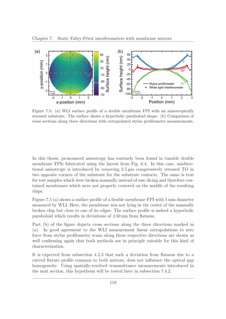
Chapter 7. Static Fabry-Perot interferometers with membrane mirrors
-2 -1 0 1 2
-2
-1
0
1
2
90°
45°
Surfaceheight(nm)
y-position(mm)
x-position (mm)
-70
-50
-30
-10
10
30
50
SampleHu169A
0°(a)
-3 -2 -1 0 1 2 3-100-80-60-40-200204060
90°
45°
Surfaceheight(nm)
Position (mm)
Stylus profilometerWhite light interferometer
SampleHu169A
0°
(b)
Figure 7.5: (a) WLI surface profile of a double membrane FPI with an anisotropicallystressed substrate. The surface shows a hyperbolic paraboloid shape. (b) Comparison ofcross sections along three directions with extrapolated stylus profilometer measurements.
In this thesis, pronounced anisotropy has routinely been found in tunable doublemembrane FPIs fabricated using the layout from Fig. 6.4. In this case, unidirec-tional anisotropy is introduced by removing . compressively stressed TO intwo opposite corners of the substrate for the substrate contacts. The same is truefor test samples which were broken manually instead of saw dicing and therefore con-tained membranes which were not properly centered on the middle of the resultingchips.
Figure 7.5 (a) shows a surface profile of a double membrane FPI with diametermeasured by WLI. Here, the membrane was not lying in the center of the manuallybroken chip but close to one of its edges. The surface profile is indeed a hyperbolicparaboloid which results in deviations of ± from flatness.
Part (b) of the figure depicts cross sections along the three directions marked in(a). In good agreement to the WLI measurement linear extrapolations to zeroforce from stylus profilometry scans along these respective directions are shown aswell confirming again that both methods are in principle suitable for this kind ofcharacterization.
It is expected from subsection 4.2.3 that such a deviation from flatness due to acurved fixture profile common to both mirrors, does not influence the optical gaphomogeneity. Using spatially-resolved transmittance measurements introduced inthe next section, this hypothesis will be tested later in subsection 7.4.2.
118
7.3 Local probing of FPIs by spatially-resolved transmittance measurements
7.3 Local probing of FPIs by spatially-resolved
transmittance measurements
It has been discussed in Eq. 3.15 that the transmittance through the full apertureof an FPI, T , corresponds to an area integration over the local transmittancecontributions. This is turn leads to transmittance peak broadening in case of aninhomogeneous optical gap. While T is the final quantity of interest for opticalFPI performance in a miniaturized spectrometer, information about, e.g., the actualmirror quality and the source of the inhomogeneity are lost due to the integration.
While the contribution of divergence finesse F is typically known from the exper-imental conditions, it is not straightforward to determine the contribution of opticalgap inhomogeneities to peak broadening. Previously, it has been attempted to es-sentially deconvolve T spectra by varying the defect contributions in a simulationuntil good agreement with the measurement was achieved [44,77]. Alternatively, thedefect finesse has been calculated from the difference between the ideal peak FWHMand the measured FWHM in order to determine an order of magnitude for gap vari-ations due to geometric defects [91]. However, since all defects essentially lead topeak broadening, none of these methods can reliably identify the actual source ofgap inhomogeneity.
A loss of information about the gap distribution can be circumvented in the firstplace if the measurement spot is limited to a small area A instead and transmit-tance is then repeatedly measured while sampling over the aperture area. If the spotsize is small enough that d can be regarded as constant, the resulting peak FWHMis limited by the reflective finesse and the spectral peak position is determined byd .
In subsection 7.3.1, a custom transmittance setup which makes use of such spatially-resolved transmittance measurements is introduced. Furthermore, possible errorsoccurring when extracting spatial optical gap maps from such measurements are ad-dressed. Subsequently, comparison with full aperture transmittance measurementsis drawn in subsection 7.3.2 in order to illustrate the benefits of this measurementstrategy.
7.3.1 Derivation of the optical gap width from spatially-resolved transmittance spectra
In order to retain maximum information about mirror quality and gap inhomo-geneities, an automated transmittance setup has been developed which is capable
119
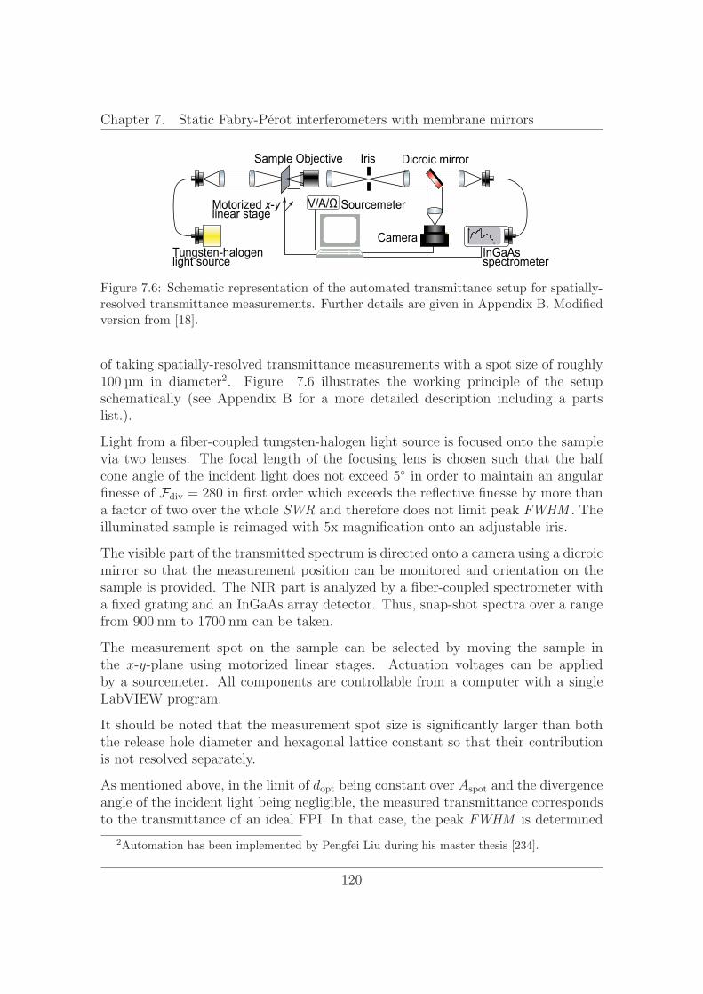
Chapter 7. Static Fabry-Perot interferometers with membrane mirrors
Tungsten-halogenlight source
Motorized x-ylinear stage
CameraInGaAsspectrometer
Iris Dicroic mirrorSample Objective
V/A/ Sourcemeter
Figure 7.6: Schematic representation of the automated transmittance setup for spatially-resolved transmittance measurements. Further details are given in Appendix B. Modifiedversion from [18].
of taking spatially-resolved transmittance measurements with a spot size of roughlyin diameter2. Figure 7.6 illustrates the working principle of the setup
schematically (see Appendix B for a more detailed description including a partslist.).
Light from a fiber-coupled tungsten-halogen light source is focused onto the samplevia two lenses. The focal length of the focusing lens is chosen such that the halfcone angle of the incident light does not exceed ◦ in order to maintain an angularfinesse of F = 280 in first order which exceeds the reflective finesse by more thana factor of two over the whole SWR and therefore does not limit peak FWHM . Theilluminated sample is reimaged with 5x magnification onto an adjustable iris.
The visible part of the transmitted spectrum is directed onto a camera using a dicroicmirror so that the measurement position can be monitored and orientation on thesample is provided. The NIR part is analyzed by a fiber-coupled spectrometer witha fixed grating and an InGaAs array detector. Thus, snap-shot spectra over a rangefrom to can be taken.
The measurement spot on the sample can be selected by moving the sample inthe x-y-plane using motorized linear stages. Actuation voltages can be appliedby a sourcemeter. All components are controllable from a computer with a singleLabVIEW program.
It should be noted that the measurement spot size is significantly larger than boththe release hole diameter and hexagonal lattice constant so that their contributionis not resolved separately.
As mentioned above, in the limit of d being constant over A and the divergenceangle of the incident light being negligible, the measured transmittance correspondsto the transmittance of an ideal FPI. In that case, the peak FWHM is determined
2Automation has been implemented by Pengfei Liu during his master thesis [234].
120
7.3 Local probing of FPIs by spatially-resolved transmittance measurements
solely by the mirror reflectances and the peak position follows from Eq. 3.9. For aknown mirror geometry and interference order, d is the only unknown in Eq. 3.9.From a locally measured transmittance peak position, d can therefore be derived(assuming an air cavity with n = 1):
d =2πm+ φ (λm) + φ (λm)
4π θλm (7.2)
Application of Eq. 7.2 requires knowledge of the wavelength-dependent phase shiftupon reflection φ , (λ). Given the individual layer thicknesses and refractiveindices, φ , (λ) can be calculated using the transfer-matrix method. In thisthesis, refractive indices of a-Si and SiCN were determined a priori by variable-angleSE and were used as fixed inputs for later fitting.
While it is possible to check individual layer thicknesses in full DBR stacks ellipso-metrically for consistency and good fits were usually achieved within ± of thenominal thicknesses, correlations between the fit parameters increases with increas-ing number of layers. Therefore, it cannot be expected that fitted thicknesses inthe calculation of φ , give better accuracy so that the nominal thicknesses weregenerally used instead.
Given also the fact that actual refractive indices depend on chamber conditioningas shown in subsection 5.2.3, φ , (λ) is an error source for the determinationof d . The magnitude of errors has been estimated by Monte-Carlo simulation ofd for first order transmittance at λ1 = assuming normally distributedmirror thicknesses and refractive indices with standard deviations of sd = andsn = 0.01, respectively. The resulting distribution of d had a standard deviationof sd, = indicating the error in optical gap estimation.
In the following, the main focus will lie on the homogeneity of the optical gap,i.e., the absolute value of d is of minor importance compared to the variation ofd over the aperture area. For a spatially-dependent gap profile determined frommapping of the measurement spot, the mirror layer refractive indices from a singledeposition can surely be regarded as constant. From typical thickness homogeneitymeasurements, it can be estimated that over the largest apertures used in this thesis( in diameter), mirror thicknesses are constant up to variation. In thatcase, the aforementioned Monte-Carlo simulations predict an accuracy for the opticalgap within the aperture area of sd, , = . which is sufficient to resolve theinhomogeneities for single membrane FPIs in subsection 7.4.1.
121
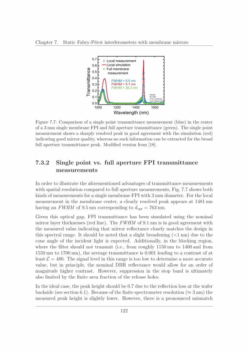
Chapter 7. Static Fabry-Perot interferometers with membrane mirrors
1000 1200 1400 16000.0
0.1
0.2
0.3
0.4
0.5
0.6
0.7
FWHM = 36.2 nm
Local measurementLocal simulationFull membranemeasurement
FWHM = 9.1 nmTransmittance
Wavelength (nm)
FWHM = 9.5 nm
SampleHu133G3 mm membrane3 μm release holes
Figure 7.7: Comparison of a single point transmittance measurement (blue) in the centerof a single membrane FPI and full aperture transmittance (green). The single pointmeasurement shows a sharply resolved peak in good agreement with the simulation (red)indicating good mirror quality, whereas no such information can be extracted for the broadfull aperture transmittance peak. Modified version from [18].
7.3.2 Single point vs. full aperture FPI transmittancemeasurements
In order to illustrate the aforementioned advantages of transmittance measurementswith spatial resolution compared to full aperture measurements, Fig. 7.7 shows bothkinds of measurements for a single membrane FPI with diameter. For the localmeasurement in the membrane center, a clearly resolved peak appears athaving an FWHM of . corresponding to d = .
Given this optical gap, FPI transmittance has been simulated using the nominalmirror layer thicknesses (red line). The FWHM of . is in good agreement withthe measured value indicating that mirror reflectance closely matches the design inthis spectral range. It should be noted that a slight broadening (< ) due to thecone angle of the incident light is expected. Additionally, in the blocking region,where the filter should not transmit (i.e., from roughly to nd from
to ), the average transmittance is 0.001 leading to a contrast of atleast C = 480. The signal level in this range is too low to determine a more accuratevalue, but in principle, the nominal DBR reflectance would allow for an order ofmagnitude higher contrast. However, suppression in the stop band is ultimatelyalso limited by the finite area fraction of the release holes.
In the ideal case, the peak height should be 0.7 due to the reflection loss at the waferbackside (see section 6.1). Because of the finite spectrometer resolution (≈ ) themeasured peak height is slightly lower. However, there is a pronounced mismatch
122
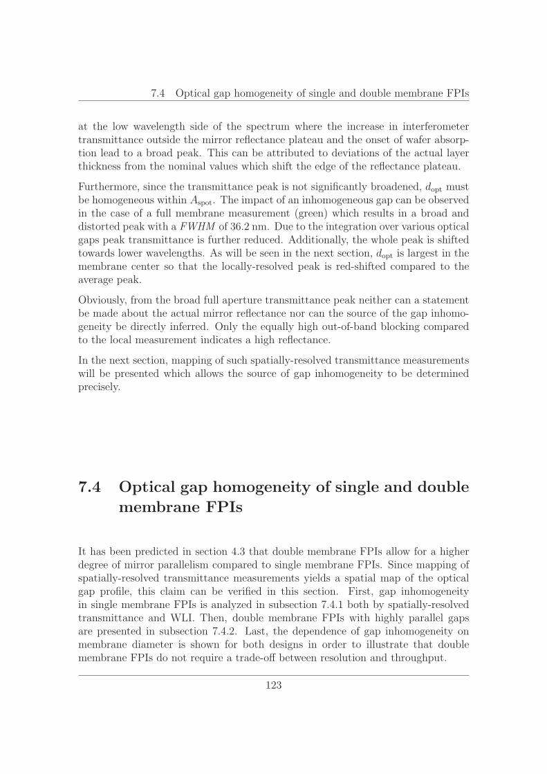
7.4 Optical gap homogeneity of single and double membrane FPIs
at the low wavelength side of the spectrum where the increase in interferometertransmittance outside the mirror reflectance plateau and the onset of wafer absorp-tion lead to a broad peak. This can be attributed to deviations of the actual layerthickness from the nominal values which shift the edge of the reflectance plateau.
Furthermore, since the transmittance peak is not significantly broadened, d mustbe homogeneous within A . The impact of an inhomogeneous gap can be observedin the case of a full membrane measurement (green) which results in a broad anddistorted peak with a FWHM of . . Due to the integration over various opticalgaps peak transmittance is further reduced. Additionally, the whole peak is shiftedtowards lower wavelengths. As will be seen in the next section, d is largest in themembrane center so that the locally-resolved peak is red-shifted compared to theaverage peak.
Obviously, from the broad full aperture transmittance peak neither can a statementbe made about the actual mirror reflectance nor can the source of the gap inhomo-geneity be directly inferred. Only the equally high out-of-band blocking comparedto the local measurement indicates a high reflectance.
In the next section, mapping of such spatially-resolved transmittance measurementswill be presented which allows the source of gap inhomogeneity to be determinedprecisely.
7.4 Optical gap homogeneity of single and double
membrane FPIs
It has been predicted in section 4.3 that double membrane FPIs allow for a higherdegree of mirror parallelism compared to single membrane FPIs. Since mapping ofspatially-resolved transmittance measurements yields a spatial map of the opticalgap profile, this claim can be verified in this section. First, gap inhomogeneityin single membrane FPIs is analyzed in subsection 7.4.1 both by spatially-resolvedtransmittance and WLI. Then, double membrane FPIs with highly parallel gapsare presented in subsection 7.4.2. Last, the dependence of gap inhomogeneity onmembrane diameter is shown for both designs in order to illustrate that doublemembrane FPIs do not require a trade-off between resolution and throughput.
123
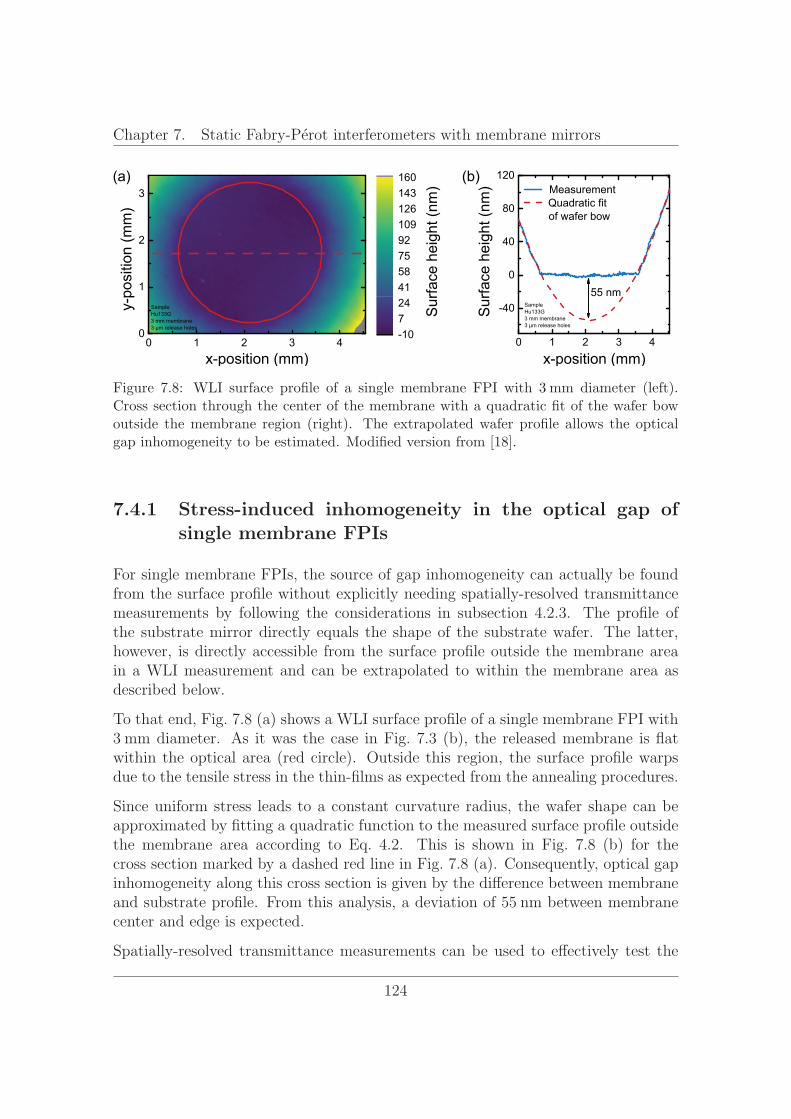
Chapter 7. Static Fabry-Perot interferometers with membrane mirrors
0 1 2 3 4
-40
0
40
80
120
SampleHu133G3 mm membrane3 μm release holes
Sur
face
hei
ght (
nm)
x-position (mm)
Measurement Quadratic fit
of wafer bow
55 nm
0 1 2 3 40
1
2
3
Sur
face
hei
ght (
nm)
y-po
sitio
n (m
m)
x-position (mm)
-1072441587592109126143160
SampleHu133G3 mm membrane3 μm release holes
(a) (b)
Figure 7.8: WLI surface profile of a single membrane FPI with diameter (left).Cross section through the center of the membrane with a quadratic fit of the wafer bowoutside the membrane region (right). The extrapolated wafer profile allows the opticalgap inhomogeneity to be estimated. Modified version from [18].
7.4.1 Stress-induced inhomogeneity in the optical gap ofsingle membrane FPIs
For single membrane FPIs, the source of gap inhomogeneity can actually be foundfrom the surface profile without explicitly needing spatially-resolved transmittancemeasurements by following the considerations in subsection 4.2.3. The profile ofthe substrate mirror directly equals the shape of the substrate wafer. The latter,however, is directly accessible from the surface profile outside the membrane areain a WLI measurement and can be extrapolated to within the membrane area asdescribed below.
To that end, Fig. 7.8 (a) shows a WLI surface profile of a single membrane FPI withdiameter. As it was the case in Fig. 7.3 (b), the released membrane is flat
within the optical area (red circle). Outside this region, the surface profile warpsdue to the tensile stress in the thin-films as expected from the annealing procedures.
Since uniform stress leads to a constant curvature radius, the wafer shape can beapproximated by fitting a quadratic function to the measured surface profile outsidethe membrane area according to Eq. 4.2. This is shown in Fig. 7.8 (b) for thecross section marked by a dashed red line in Fig. 7.8 (a). Consequently, optical gapinhomogeneity along this cross section is given by the difference between membraneand substrate profile. From this analysis, a deviation of between membranecenter and edge is expected.
Spatially-resolved transmittance measurements can be used to effectively test the
124
7.4 Optical gap homogeneity of single and double membrane FPIs
0 1 2 30
1
2
3
SampleHu133G3 mm membrane3 μm release holes
Opticalgap(nm)
y-position(mm)
x-position (mm)
699
712
726
739
753
766(a)
0 1 2 3
0
20
40
60
SampleHu133G3 mm membrane3 μm release holes
Opticalgapvariation(nm)
x-position (mm)
White light interferometerTransmittance mapping
(b)
Figure 7.9: (a) Optical gap map of a single membrane FPI with diameter fromspatially-resolved transmittance measurements and (b) comparison of the optical gap vari-ation along the dashed red line with the gap variation deduced from Fig. 7.8 (right): Therotationally symmetric profile and good agreement with the WLI data indicate that thewafer bow is the source of the gap inhomogeneity. Modified version from [18].
validity of the approach above. Accordingly, Fig. 7.9 (a) shows a map of the opti-cal gap for the same single membrane FPI as in Fig. 7.8 which has been deducedfrom spatially-resolved transmittance measurements as outlined in subsection 7.3.1.The profile is rotationally symmetric as it would be expected for a uniform stress.Furthermore, d is largest in the middle which explains the red-shift of the locallyresolved peak in Fig. 7.7 compared to the full aperture transmittance.
The right side of Fig. 7.9 depicts the variation of d along the dashed red line to-gether with the variation given by the difference between the mirror profiles from theWLI measurement in Fig. 7.8. The two cross sections largely coincide. Accordingly,gap inhomogeneity in single membrane FPIs (directly measured by spatially-resolvedtransmittance) is caused primarily by the bow of the substrate wafer (extracted fromthe WLI surface profile) confirming the respective hypothesis from subsection 4.2.3.
7.4.2 Double membrane FPIs with highly homogeneousoptical gaps
As discussed in section 4.3, double membrane FPIs circumvent the dependence ofmirror parallelism on wafer bow by decoupling both mirrors from the substratewithin the optical aperture. For better comparison with the single membrane FPIdata shown above, diameter samples are considered for the double membraneFPIs as well.
125
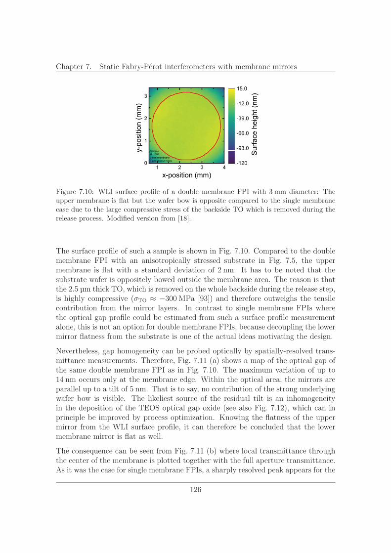
Chapter 7. Static Fabry-Perot interferometers with membrane mirrors
1 2 3 40
1
2
3
SampleHu169F3 mm membrane3 μm release holes
Sur
face
hei
ght (
nm)
y-po
sitio
n (m
m)
x-position (mm)
-120
-93.0
-66.0
-39.0
-12.0
15.0
Figure 7.10: WLI surface profile of a double membrane FPI with diameter: Theupper membrane is flat but the wafer bow is opposite compared to the single membranecase due to the large compressive stress of the backside TO which is removed during therelease process. Modified version from [18].
The surface profile of such a sample is shown in Fig. 7.10. Compared to the doublemembrane FPI with an anisotropically stressed substrate in Fig. 7.5, the uppermembrane is flat with a standard deviation of . It has to be noted that thesubstrate wafer is oppositely bowed outside the membrane area. The reason is thatthe . thick TO, which is removed on the whole backside during the release step,is highly compressive (σ ≈ − [93]) and therefore outweighs the tensilecontribution from the mirror layers. In contrast to single membrane FPIs wherethe optical gap profile could be estimated from such a surface profile measurementalone, this is not an option for double membrane FPIs, because decoupling the lowermirror flatness from the substrate is one of the actual ideas motivating the design.
Nevertheless, gap homogeneity can be probed optically by spatially-resolved trans-mittance measurements. Therefore, Fig. 7.11 (a) shows a map of the optical gap ofthe same double membrane FPI as in Fig. 7.10. The maximum variation of up to
occurs only at the membrane edge. Within the optical area, the mirrors areparallel up to a tilt of . That is to say, no contribution of the strong underlyingwafer bow is visible. The likeliest source of the residual tilt is an inhomogeneityin the deposition of the TEOS optical gap oxide (see also Fig. 7.12), which can inprinciple be improved by process optimization. Knowing the flatness of the uppermirror from the WLI surface profile, it can therefore be concluded that the lowermembrane mirror is flat as well.
The consequence can be seen from Fig. 7.11 (b) where local transmittance throughthe center of the membrane is plotted together with the full aperture transmittance.As it was the case for single membrane FPIs, a sharply resolved peak appears for the
126
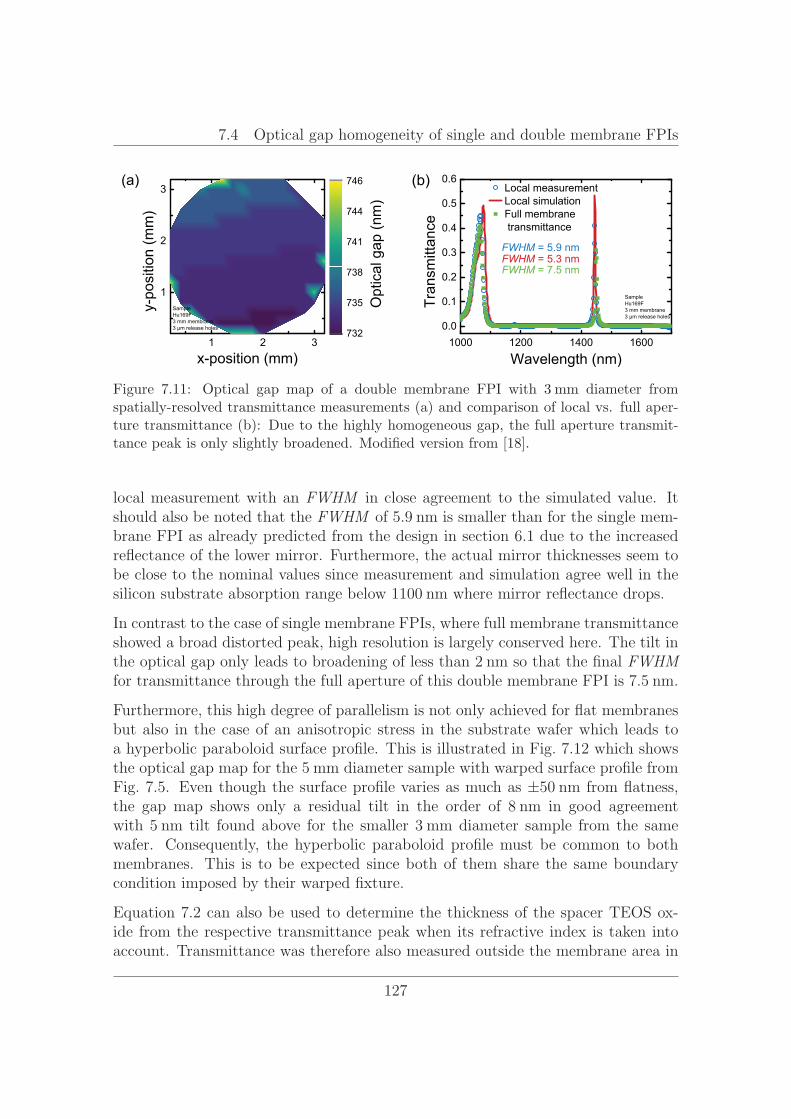
7.4 Optical gap homogeneity of single and double membrane FPIs
1 2 3
1
2
3
SampleHu169F3 mm membrane3 μm release holes
Opticalgap(nm)
y-position(mm)
x-position (mm)
732
735
738
741
744
746(a)
1000 1200 1400 16000.0
0.1
0.2
0.3
0.4
0.5
0.6
SampleHu169F3 mm membrane3 μm release holes
Transmittance
Wavelength (nm)
Local measurementLocal simulationFull membranetransmittance
FWHM = 5.9 nmFWHM = 5.3 nmFWHM = 7.5 nm
(b)
Figure 7.11: Optical gap map of a double membrane FPI with diameter fromspatially-resolved transmittance measurements (a) and comparison of local vs. full aper-ture transmittance (b): Due to the highly homogeneous gap, the full aperture transmit-tance peak is only slightly broadened. Modified version from [18].
local measurement with an FWHM in close agreement to the simulated value. Itshould also be noted that the FWHM of . is smaller than for the single mem-brane FPI as already predicted from the design in section 6.1 due to the increasedreflectance of the lower mirror. Furthermore, the actual mirror thicknesses seem tobe close to the nominal values since measurement and simulation agree well in thesilicon substrate absorption range below where mirror reflectance drops.
In contrast to the case of single membrane FPIs, where full membrane transmittanceshowed a broad distorted peak, high resolution is largely conserved here. The tilt inthe optical gap only leads to broadening of less than so that the final FWHMfor transmittance through the full aperture of this double membrane FPI is . .
Furthermore, this high degree of parallelism is not only achieved for flat membranesbut also in the case of an anisotropic stress in the substrate wafer which leads toa hyperbolic paraboloid surface profile. This is illustrated in Fig. 7.12 which showsthe optical gap map for the diameter sample with warped surface profile fromFig. 7.5. Even though the surface profile varies as much as ± from flatness,the gap map shows only a residual tilt in the order of in good agreementwith tilt found above for the smaller diameter sample from the samewafer. Consequently, the hyperbolic paraboloid profile must be common to bothmembranes. This is to be expected since both of them share the same boundarycondition imposed by their warped fixture.
Equation 7.2 can also be used to determine the thickness of the spacer TEOS ox-ide from the respective transmittance peak when its refractive index is taken intoaccount. Transmittance was therefore also measured outside the membrane area in
127
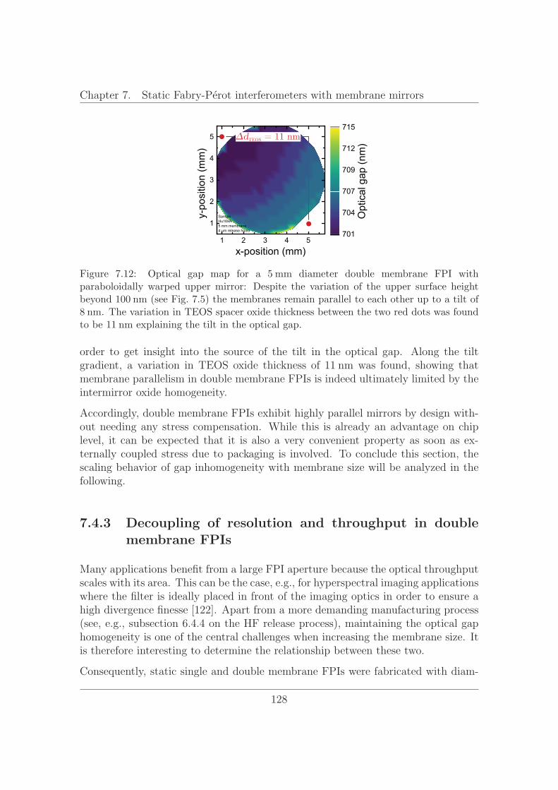
Chapter 7. Static Fabry-Perot interferometers with membrane mirrors
1 2 3 4 5
1
2
3
4
5
Opt
ical
gap
(nm
)
SampleHu169A5 mm membrane4 μm release holes
y-po
sitio
n (m
m)
x-position (mm)
701
704
707
709
712
715
Figure 7.12: Optical gap map for a diameter double membrane FPI withparaboloidally warped upper mirror: Despite the variation of the upper surface heightbeyond (see Fig. 7.5) the membranes remain parallel to each other up to a tilt of
. The variation in TEOS spacer oxide thickness between the two red dots was foundto be explaining the tilt in the optical gap.
order to get insight into the source of the tilt in the optical gap. Along the tiltgradient, a variation in TEOS oxide thickness of was found, showing thatmembrane parallelism in double membrane FPIs is indeed ultimately limited by theintermirror oxide homogeneity.
Accordingly, double membrane FPIs exhibit highly parallel mirrors by design with-out needing any stress compensation. While this is already an advantage on chiplevel, it can be expected that it is also a very convenient property as soon as ex-ternally coupled stress due to packaging is involved. To conclude this section, thescaling behavior of gap inhomogeneity with membrane size will be analyzed in thefollowing.
7.4.3 Decoupling of resolution and throughput in doublemembrane FPIs
Many applications benefit from a large FPI aperture because the optical throughputscales with its area. This can be the case, e.g., for hyperspectral imaging applicationswhere the filter is ideally placed in front of the imaging optics in order to ensure ahigh divergence finesse [122]. Apart from a more demanding manufacturing process(see, e.g., subsection 6.4.4 on the HF release process), maintaining the optical gaphomogeneity is one of the central challenges when increasing the membrane size. Itis therefore interesting to determine the relationship between these two.
Consequently, static single and double membrane FPIs were fabricated with diam-
128
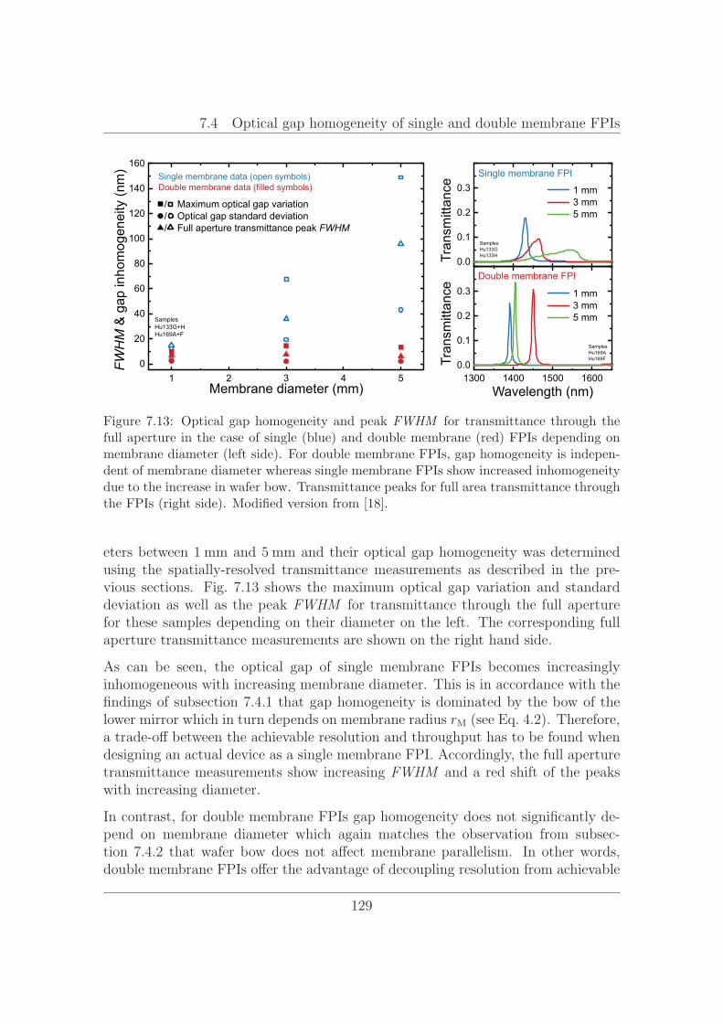
7.4 Optical gap homogeneity of single and double membrane FPIs
1 2 3 4 50
20
40
60
80
100
120
140
160
FWHM
& g
ap in
hom
ogen
eity
(nm
)
/ Maximum optical gap variation/ Optical gap standard deviation/ Full aperture transmittance peak FWHM
Membrane diameter (mm)
SamplesHu133G+HHu169A+F
Single membrane data (open symbols)Double membrane data (filled symbols)
0.0
0.1
0.2
0.3
Tran
smitt
ance 1 mm
3 mm5 mm
SamplesHu133GHu133H
Single membrane FPI
1300 1400 1500 16000.0
0.1
0.2
0.3
SamplesHu169AHu169FTr
ansm
ittan
ce
Wavelength (nm)
1 mm3 mm5 mm
Double membrane FPI
Figure 7.13: Optical gap homogeneity and peak FWHM for transmittance through thefull aperture in the case of single (blue) and double membrane (red) FPIs depending onmembrane diameter (left side). For double membrane FPIs, gap homogeneity is indepen-dent of membrane diameter whereas single membrane FPIs show increased inhomogeneitydue to the increase in wafer bow. Transmittance peaks for full area transmittance throughthe FPIs (right side). Modified version from [18].
eters between and and their optical gap homogeneity was determinedusing the spatially-resolved transmittance measurements as described in the pre-vious sections. Fig. 7.13 shows the maximum optical gap variation and standarddeviation as well as the peak FWHM for transmittance through the full aperturefor these samples depending on their diameter on the left. The corresponding fullaperture transmittance measurements are shown on the right hand side.
As can be seen, the optical gap of single membrane FPIs becomes increasinglyinhomogeneous with increasing membrane diameter. This is in accordance with thefindings of subsection 7.4.1 that gap homogeneity is dominated by the bow of thelower mirror which in turn depends on membrane radius r (see Eq. 4.2). Therefore,a trade-off between the achievable resolution and throughput has to be found whendesigning an actual device as a single membrane FPI. Accordingly, the full aperturetransmittance measurements show increasing FWHM and a red shift of the peakswith increasing diameter.
In contrast, for double membrane FPIs gap homogeneity does not significantly de-pend on membrane diameter which again matches the observation from subsec-tion 7.4.2 that wafer bow does not affect membrane parallelism. In other words,double membrane FPIs offer the advantage of decoupling resolution from achievable
129
Chapter 7. Static Fabry-Perot interferometers with membrane mirrors
throughput at least within the fabricated range of membrane diameters. However,there is no a priori reason to assume that FPIs with larger membrane diametersshould behave differently. When comparing the full aperture transmittance mea-surements it should be noted, that it was not possible to fully limit detected lightto the membrane area for the smallest sample with diameter which is whythe peak transmittance is appears reduced. The actual position of the peaks de-pends on the local TEOS oxide thickness which varies slightly at different positionson the wafer. Nevertheless, it can be seen that the peaks do not broadensignificantly.
It should be noted that there are measures to improve membrane parallelism in singlemembrane FPIs. Bow depends inversely quadratically on substrate thickness, so thata thicker substrate wafer can significantly improve gap homogeneity. Alternatively,stress compensation layers can be deposited on the wafer backside (at least outsidethe optical aperture). However, as stated before other factors apart from thin-filmstress can cause substrate bow such as chip packaging [5] and interconnects so thatthe inherent robustness of double membrane FPIs against induced stress is certainlyadvantageous.
7.5 Summary: Double membrane FPIs for large-
area, high-resolution filters
In short, the static behavior of both single and double membrane first order FPIs hasbeen thoroughly characterized in this chapter. It could be confirmed by LDV thatthe fundamental resonance frequency of released membrane DBRs lies far abovetypical external disturbing frequencies which preferably should not couple to thedevice. The spectral position of the vibrational eigenmodes was furthermore usedto extract the tensile stress level of such membranes. It should be noted that thismethod has so far not commonly been used in the MEMS FPI community.
Released membranes are exceptionally flat with nanometer standard deviations evenfor large membrane diameters as evidenced both from mechanical stylus profilometryand WLI. However, if the substrate is subject to an anisotropic in-plane stress,membranes are deformed to a hyperbolic paraboloid according to the sinusoidalfixture profile.
Both single and double membrane FPIs locally work as narrow-band optical filters inthe NIR with a resolution below in the range of the design wavelength of theDBRs and suppression in the stop band with a contrast of around 400. However, forlarge membrane diameters in the millimeter range the full aperture transmittance
130
7.5 Summary: Double membrane FPIs for large-area, high-resolution filters
of single membrane FPIs is dominated by the low defect finesse associated withan inhomogeneity in the optical gap due to the bow of the substrate wafer. Dou-ble membrane FPIs on the other hand show highly parallel mirrors even fordiameter membranes, i.e., resolution and throughput are essentially decoupled. Mir-rors remain parallel even if the membranes are not flat but share the aforementionedhyperbolic paraboloid profile. It is expected that this insensitivity of mirror paral-lelism to substrate warp will also prove useful when external stress factors such aschip packaging are considered.
A key element in the characterization, which allowed an unambiguous assignmentof the source of single membrane FPI gap inhomogeneity to wafer bow, was the useof spatially-resolved transmittance measurements instead of full aperture transmit-tance. For double membrane FPIs such measurements provide a non-destructivemeans to measure the profile of the lower membrane mirror which would otherwiseonly be accessible by removing the upper mirror.
High mirror parallelism has been one of the advantages of the double membraneFPI structure which has been claimed in section 4.3. The other one, namely theincreased tuning range which enables resonance tuning over the full first FSR willbe examined in the following chapter.
131

Chapter 7. Static Fabry-Perot interferometers with membrane mirrors
132
Chapter 8
Actuated Fabry-Perotinterferometers
Apart from the high degree of parallelism achievable by the double membrane FPIapproach, the increase of available travel range before electrostatic pull-in occursis the other benefit claimed in section 4.3. This is enabled by pulling the lowermembrane down to the substrate, so that the initial actuation gap d , is determinedby the thickness of the sacrificial oxide d separating these two, which can be chosenindependently from the initial optical gap d , .
As described in section 6.3, the mirrors of the static filters from the previous chaptersneed at least one conducting layer which can be contacted from outside in order toenable actuation. To that end, the single and double membrane FPIs used for thischapter were fabricated with the last of both mirrors being boron-doped μc-Si. Using the contact openings in the chip corners, actuation voltages U couldthen be applied using spring-loaded test pins with the FPIs mounted to a customenclosure as described in Appendix B.
The chapter starts with a detailed analysis of single membrane FPIs during actuationand thereby shows that electrostatic pull-in occurs while tuning the transmittancewavelength within the first FSR. In the second part, actuated double membraneFPIs will be presented which exhibit a larger stable travel range sufficient to coverthe full first FSR.
Parts of the results shown in this chapter have been published in [23].
133
Chapter 8. Actuated Fabry-Perot interferometers
8.1 Actuated single membrane FPIs limited by
electrostatic pull-in
For an actuated single membrane FPI the initial optical gap d , , i.e., the thicknessof the sacrificial oxide, has to be chosen such that it results in transmittance atλ , , the upper end of the desired SWR. As described in section 6.1, for Si/SiCNDBRs this leads to d , = for transmittance at λ , = .
However, the available measurement range of the InGaAs spectrometer used fortransmittance measurements ends at . Furthermore, single membrane FPIscan be expected to have a larger d , in the membrane center due to the bow inthe substrate wafer as shown in the previous chapter. Therefore, the FPIs in thischapter were deposited with a smaller nominal TEOS thickness of d ≈in order to ensure that the first order transmittance peak lies in the measurementrange for all applied actuation voltages U .
Such single membrane FPIs have been successfully fabricated with diameters of, and , all of them being functional. However, despite the reduced
TEOS thickness, the first order transmittance peak in the rest position was lyingoutside of the measurement range for the samples. Therefore, the resultsshown in this section stem from filters with diameter.
8.1.1 The surface profile of the moving membrane mirror
In the case of single membrane FPIs, the upper mirror membrane is displaced to-wards the substrate during actuation. Therefore, WLI can be used to directly mo-nitor this displacement by measuring the surface profile while an actuation voltageU is applied. Figure 8.1 (a) shows a series of cross sections at the same positionof a single membrane FPI with diameter recorded for actuation voltages Uup to in steps of . with an additional measurement at U = . .
It should be noted at this point, that the force which is exerted on the chip bythe spring-loaded test pins leads to additional strain in the chip. Therefore, themirror surface of an FPI mounted in the contacting enclosure is not flat even if it isflat in the unmounted case. Instead, it shows a curvature similar to the hyperbolicparaboloids known from an anisotropic in-plane stress described in subsection 4.2.3.For reasons of a better readability, the direction of the plotted membrane crosssections in Fig. 8.1 (a) have been chosen such that the membrane appears flat alongthis direction (see Fig. 8.5 (a) for an example).
134
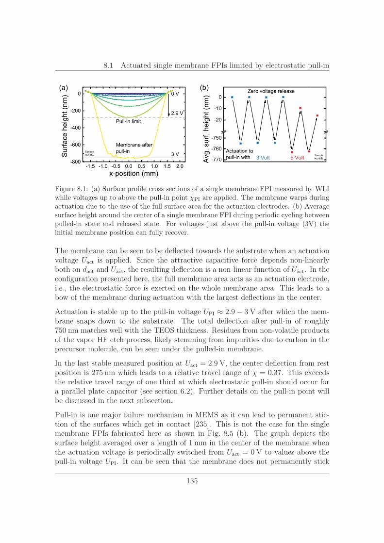
8.1 Actuated single membrane FPIs limited by electrostatic pull-in
-1.5 -1.0 -0.5 0.0 0.5 1.0 1.5 2.0-800
-600
-400
-200
0
Membrane afterpull-in 3 V
2.9 V
Surfaceheight(nm)
x-position (mm)
0 V
Pull-in limit
SampleHu185L
(a)
-770
-760
-750
-20
-10
0
(b)
SampleHu185L5 VoltA
vg.surf.height(nm)
Zero voltage release
Actuation topull-in with 3 Volt
Figure 8.1: (a) Surface profile cross sections of a single membrane FPI measured by WLIwhile voltages up to above the pull-in point χ are applied. The membrane warps duringactuation due to the use of the full surface area for the actuation electrodes. (b) Averagesurface height around the center of a single membrane FPI during periodic cycling betweenpulled-in state and released state. For voltages just above the pull-in voltage (3V) theinitial membrane position can fully recover.
The membrane can be seen to be deflected towards the substrate when an actuationvoltage U is applied. Since the attractive capacitive force depends non-linearlyboth on d and U , the resulting deflection is a non-linear function of U . In theconfiguration presented here, the full membrane area acts as an actuation electrode,i.e., the electrostatic force is exerted on the whole membrane area. This leads to abow of the membrane during actuation with the largest deflections in the center.
Actuation is stable up to the pull-in voltage U ≈ . − after which the mem-brane snaps down to the substrate. The total deflection after pull-in of roughly
matches well with the TEOS thickness. Residues from non-volatile productsof the vapor HF etch process, likely stemming from impurities due to carbon in theprecursor molecule, can be seen under the pulled-in membrane.
In the last stable measured position at U = . , the center deflection from restposition is which leads to a relative travel range of χ = 0.37. This exceedsthe relative travel range of one third at which electrostatic pull-in should occur fora parallel plate capacitor (see section 6.2). Further details on the pull-in point willbe discussed in the next subsection.
Pull-in is one major failure mechanism in MEMS as it can lead to permanent stic-tion of the surfaces which get in contact [235]. This is not the case for the singlemembrane FPIs fabricated here as shown in Fig. 8.5 (b). The graph depicts thesurface height averaged over a length of in the center of the membrane whenthe actuation voltage is periodically switched from U = to values above thepull-in voltage U . It can be seen that the membrane does not permanently stick
135
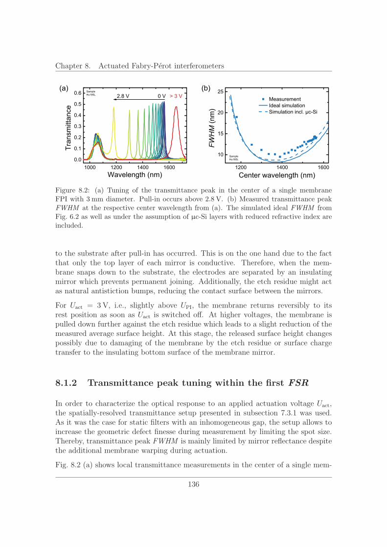
Chapter 8. Actuated Fabry-Perot interferometers
1000 1200 1400 16000.0
0.1
0.2
0.3
0.4
0.5
0.6 > 3 V2.8 V
Transmittance
Wavelength (nm)
SampleHu185L 0 V
(a)
1200 1400 1600
10
15
20
25(b)
SampleHu185L
MeasurementIdeal simulationSimulation incl. μc-Si
FWHM(nm)
Center wavelength (nm)
Figure 8.2: (a) Tuning of the transmittance peak in the center of a single membraneFPI with diameter. Pull-in occurs above . . (b) Measured transmittance peakFWHM at the respective center wavelength from (a). The simulated ideal FWHM fromFig. 6.2 as well as under the assumption of μc-Si layers with reduced refractive index areincluded.
to the substrate after pull-in has occurred. This is on the one hand due to the factthat only the top layer of each mirror is conductive. Therefore, when the mem-brane snaps down to the substrate, the electrodes are separated by an insulatingmirror which prevents permanent joining. Additionally, the etch residue might actas natural antistiction bumps, reducing the contact surface between the mirrors.
For U = , i.e., slightly above U , the membrane returns reversibly to itsrest position as soon as U is switched off. At higher voltages, the membrane ispulled down further against the etch residue which leads to a slight reduction of themeasured average surface height. At this stage, the released surface height changespossibly due to damaging of the membrane by the etch residue or surface chargetransfer to the insulating bottom surface of the membrane mirror.
8.1.2 Transmittance peak tuning within the first FSR
In order to characterize the optical response to an applied actuation voltage U ,the spatially-resolved transmittance setup presented in subsection 7.3.1 was used.As it was the case for static filters with an inhomogeneous gap, the setup allows toincrease the geometric defect finesse during measurement by limiting the spot size.Thereby, transmittance peak FWHM is mainly limited by mirror reflectance despitethe additional membrane warping during actuation.
Fig. 8.2 (a) shows local transmittance measurements in the center of a single mem-
136
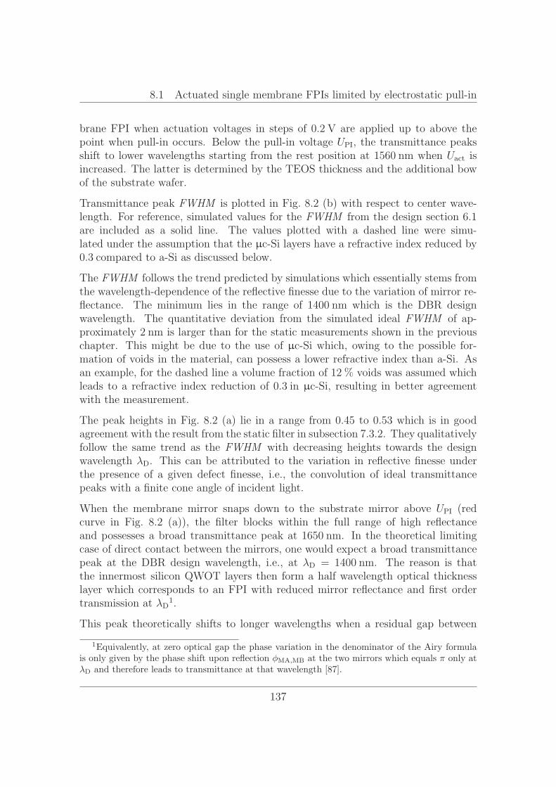
8.1 Actuated single membrane FPIs limited by electrostatic pull-in
brane FPI when actuation voltages in steps of . are applied up to above thepoint when pull-in occurs. Below the pull-in voltage U , the transmittance peaksshift to lower wavelengths starting from the rest position at when U isincreased. The latter is determined by the TEOS thickness and the additional bowof the substrate wafer.
Transmittance peak FWHM is plotted in Fig. 8.2 (b) with respect to center wave-length. For reference, simulated values for the FWHM from the design section 6.1are included as a solid line. The values plotted with a dashed line were simu-lated under the assumption that the μc-Si layers have a refractive index reduced by. ompared to a-Si as discussed below.
The FWHM follows the trend predicted by simulations which essentially stems fromthe wavelength-dependence of the reflective finesse due to the variation of mirror re-flectance. The minimum lies in the range of which is the DBR designwavelength. The quantitative deviation from the simulated ideal FWHM of ap-proximately is larger than for the static measurements shown in the previouschapter. This might be due to the use of μc-Si which, owing to the possible for-mation of voids in the material, can possess a lower refractive index than a-Si. Asan example, for the dashed line a volume fraction of voids was assumed whichleads to a refractive index reduction of . n μc-Si, resulting in better agreementwith the measurement.
The peak heights in Fig. 8.2 (a) lie in a range from 0.45 to 0.53 which is in goodagreement with the result from the static filter in subsection 7.3.2. They qualitativelyfollow the same trend as the FWHM with decreasing heights towards the designwavelength λ . This can be attributed to the variation in reflective finesse underthe presence of a given defect finesse, i.e., the convolution of ideal transmittancepeaks with a finite cone angle of incident light.
When the membrane mirror snaps down to the substrate mirror above U (redcurve in Fig. 8.2 (a)), the filter blocks within the full range of high reflectanceand possesses a broad transmittance peak at . In the theoretical limitingcase of direct contact between the mirrors, one would expect a broad transmittancepeak at the DBR design wavelength, i.e., at λ = . The reason is thatthe innermost silicon QWOT layers then form a half wavelength optical thicknesslayer which corresponds to an FPI with reduced mirror reflectance and first ordertransmission at λ 1.
This peak theoretically shifts to longer wavelengths when a residual gap between
1Equivalently, at zero optical gap the phase variation in the denominator of the Airy formulais only given by the phase shift upon reflection φ , at the two mirrors which equals π only atλ and therefore leads to transmittance at that wavelength [87].
137
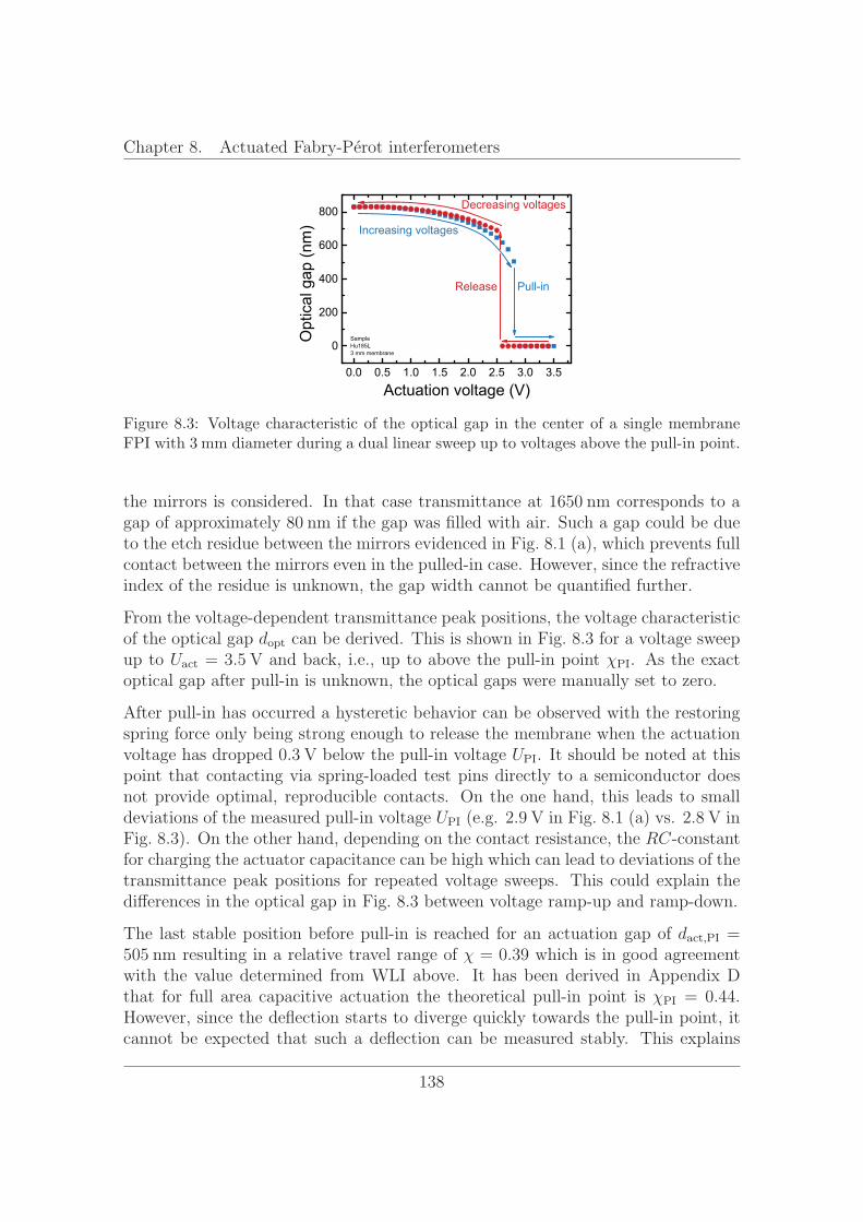
Chapter 8. Actuated Fabry-Perot interferometers
0.0 0.5 1.0 1.5 2.0 2.5 3.0 3.5
0
200
400
600
800
Opt
ical
gap
(nm
)
Actuation voltage (V)
Decreasing voltages
Increasing voltages
Pull-inRelease
SampleHu185L3 mm membrane
Figure 8.3: Voltage characteristic of the optical gap in the center of a single membraneFPI with diameter during a dual linear sweep up to voltages above the pull-in point.
the mirrors is considered. In that case transmittance at corresponds to agap of approximately if the gap was filled with air. Such a gap could be dueto the etch residue between the mirrors evidenced in Fig. 8.1 (a), which prevents fullcontact between the mirrors even in the pulled-in case. However, since the refractiveindex of the residue is unknown, the gap width cannot be quantified further.
From the voltage-dependent transmittance peak positions, the voltage characteristicof the optical gap d can be derived. This is shown in Fig. 8.3 for a voltage sweepup to U = . and back, i.e., up to above the pull-in point χ . As the exactoptical gap after pull-in is unknown, the optical gaps were manually set to zero.
After pull-in has occurred a hysteretic behavior can be observed with the restoringspring force only being strong enough to release the membrane when the actuationvoltage has dropped . below the pull-in voltage U . It should be noted at thispoint that contacting via spring-loaded test pins directly to a semiconductor doesnot provide optimal, reproducible contacts. On the one hand, this leads to smalldeviations of the measured pull-in voltage U (e.g. . in Fig. 8.1 (a) vs. . inFig. 8.3). On the other hand, depending on the contact resistance, the RC-constantfor charging the actuator capacitance can be high which can lead to deviations of thetransmittance peak positions for repeated voltage sweeps. This could explain thedifferences in the optical gap in Fig. 8.3 between voltage ramp-up and ramp-down.
The last stable position before pull-in is reached for an actuation gap of d , =resulting in a relative travel range of χ = 0.39 which is in good agreement
with the value determined from WLI above. It has been derived in Appendix Dthat for full area capacitive actuation the theoretical pull-in point is χ = 0.44.However, since the deflection starts to diverge quickly towards the pull-in point, itcannot be expected that such a deflection can be measured stably. This explains
138
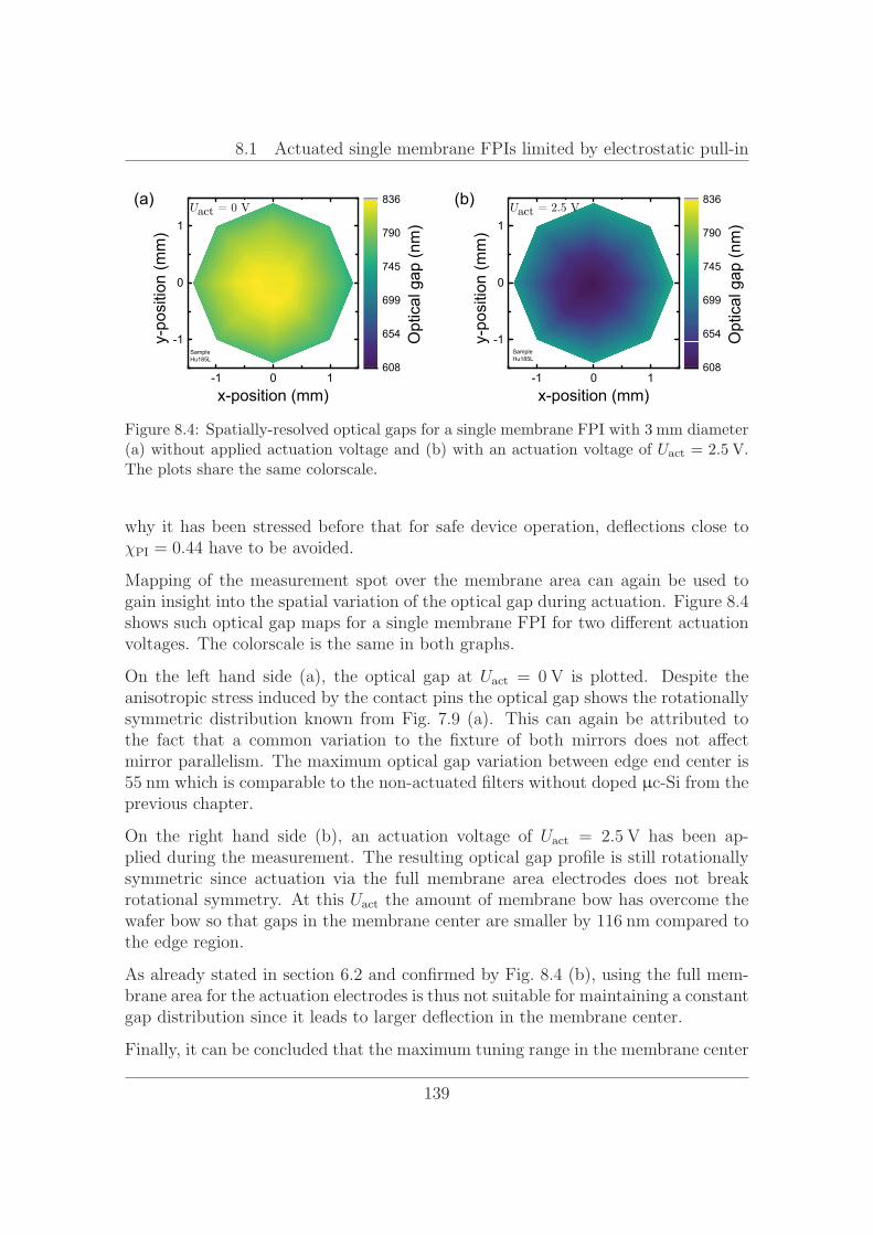
8.1 Actuated single membrane FPIs limited by electrostatic pull-in
-1 0 1
-1
0
1
SampleHu185L
Opt
ical
gap
(nm
)
y-po
sitio
n (m
m)
x-position (mm)
608
654
699
745
790
836(a)
-1 0 1
-1
0
1
(b)
SampleHu185L
Opt
ical
gap
(nm
)
y-po
sitio
n (m
m)
x-position (mm)
608
654
699
745
790
836
Figure 8.4: Spatially-resolved optical gaps for a single membrane FPI with diameter(a) without applied actuation voltage and (b) with an actuation voltage of U = . .The plots share the same colorscale.
why it has been stressed before that for safe device operation, deflections close toχ = 0.44 have to be avoided.
Mapping of the measurement spot over the membrane area can again be used togain insight into the spatial variation of the optical gap during actuation. Figure 8.4shows such optical gap maps for a single membrane FPI for two different actuationvoltages. The colorscale is the same in both graphs.
On the left hand side (a), the optical gap at U = is plotted. Despite theanisotropic stress induced by the contact pins the optical gap shows the rotationallysymmetric distribution known from Fig. 7.9 (a). This can again be attributed tothe fact that a common variation to the fixture of both mirrors does not affectmirror parallelism. The maximum optical gap variation between edge end center is
which is comparable to the non-actuated filters without doped μc-Si from theprevious chapter.
On the right hand side (b), an actuation voltage of U = . has been ap-plied during the measurement. The resulting optical gap profile is still rotationallysymmetric since actuation via the full membrane area electrodes does not breakrotational symmetry. At this U the amount of membrane bow has overcome thewafer bow so that gaps in the membrane center are smaller by compared tothe edge region.
As already stated in section 6.2 and confirmed by Fig. 8.4 (b), using the full mem-brane area for the actuation electrodes is thus not suitable for maintaining a constantgap distribution since it leads to larger deflection in the membrane center.
Finally, it can be concluded that the maximum tuning range in the membrane center
139
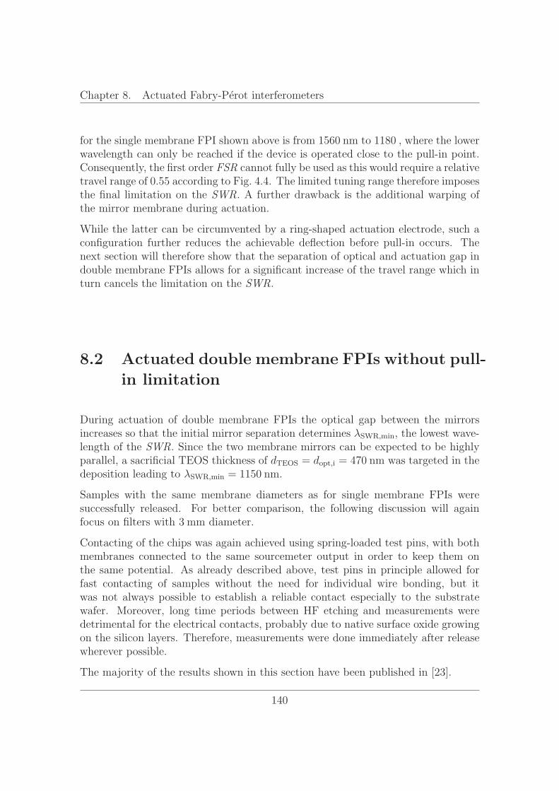
Chapter 8. Actuated Fabry-Perot interferometers
for the single membrane FPI shown above is from to , where the lowerwavelength can only be reached if the device is operated close to the pull-in point.Consequently, the first order FSR cannot fully be used as this would require a relativetravel range of 0.55 according to Fig. 4.4. The limited tuning range therefore imposesthe final limitation on the SWR. A further drawback is the additional warping ofthe mirror membrane during actuation.
While the latter can be circumvented by a ring-shaped actuation electrode, such aconfiguration further reduces the achievable deflection before pull-in occurs. Thenext section will therefore show that the separation of optical and actuation gap indouble membrane FPIs allows for a significant increase of the travel range which inturn cancels the limitation on the SWR.
8.2 Actuated double membrane FPIs without pull-
in limitation
During actuation of double membrane FPIs the optical gap between the mirrorsincreases so that the initial mirror separation determines λ , , the lowest wave-length of the SWR. Since the two membrane mirrors can be expected to be highlyparallel, a sacrificial TEOS thickness of d = d , = was targeted in thedeposition leading to λ , = .
Samples with the same membrane diameters as for single membrane FPIs weresuccessfully released. For better comparison, the following discussion will againfocus on filters with diameter.
Contacting of the chips was again achieved using spring-loaded test pins, with bothmembranes connected to the same sourcemeter output in order to keep them onthe same potential. As already described above, test pins in principle allowed forfast contacting of samples without the need for individual wire bonding, but itwas not always possible to establish a reliable contact especially to the substratewafer. Moreover, long time periods between HF etching and measurements weredetrimental for the electrical contacts, probably due to native surface oxide growingon the silicon layers. Therefore, measurements were done immediately after releasewherever possible.
The majority of the results shown in this section have been published in [23].
140
8.2 Actuated double membrane FPIs without pull-in limitation
Uact
1 2 30
1
2
3
Sur
face
hei
ght (
nm)
y-po
sitio
n (m
m)
x-position (mm)
-34
-12
10
31
53
SampleHu192B
-1.5 -1.0 -0.5 0.0 0.5 1.0 1.5-4
-2
0
2
4
6
8
10 9 V
Sur
face
hei
ght (
nm)
Position (mm)
0 V
SampleHu192B
(a) (b)
(c) (d)
SampleHu192B
500 μm
act = 0 V
SampleHu192B
500 μm
act = 9 V
Figure 8.5: (a) Surface profile of a double membrane FPI with diameter placed in thecontact pin mount and measured by WLI. The external force exerted by the contact pinsdeforms the substrate. (b) Cross section along the red line in (a) measured at actuationvoltages between and . The position of the upper mirror is not affected by theactuation voltage. (c,d) WLI camera image at (c) and (d) actuation voltage.Warping of the lower membrane during movement under the motionless upper membraneis evidenced by interference fringes.
8.2.1 The influence of actuation voltages on the uppermembrane mirror profile
While WLI could be used for single membrane FPIs to monitor the displacementof the membrane mirror, the upper membrane is now held on the same potentialas the lower membrane and should therefore not move during actuation. In orderto verify this behavior, Fig. 8.5 (a) shows the surface profile of a double membraneFPI mounted to the contact pin enclosure.
As mentioned above, the membrane surface is additionally warped due to the forceexerted by the contact pins. The cross sections in Fig. 8.5 (b) have therefore beenchosen along the red line in (a) where only small deviations from planarity occurwithin the membrane area. When the actuation voltage is increased from U =to U = no change in the upper membrane surface height is visible from the
141
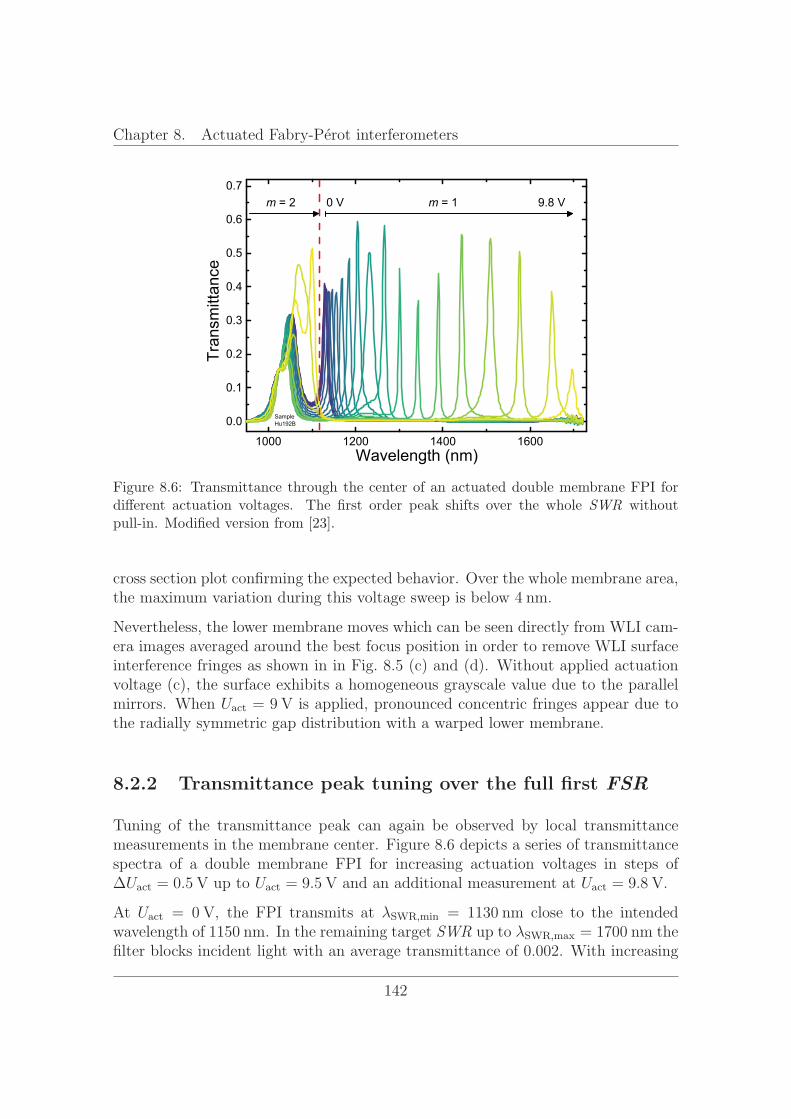
Chapter 8. Actuated Fabry-Perot interferometers
1000 1200 1400 1600
0.0
0.1
0.2
0.3
0.4
0.5
0.6
0.79.8 V
Transmittance
Wavelength (nm)
0 V m = 1m = 2
SampleHu192B
Figure 8.6: Transmittance through the center of an actuated double membrane FPI fordifferent actuation voltages. The first order peak shifts over the whole SWR withoutpull-in. Modified version from [23].
cross section plot confirming the expected behavior. Over the whole membrane area,the maximum variation during this voltage sweep is below .
Nevertheless, the lower membrane moves which can be seen directly from WLI cam-era images averaged around the best focus position in order to remove WLI surfaceinterference fringes as shown in in Fig. 8.5 (c) and (d). Without applied actuationvoltage (c), the surface exhibits a homogeneous grayscale value due to the parallelmirrors. When U = is applied, pronounced concentric fringes appear due tothe radially symmetric gap distribution with a warped lower membrane.
8.2.2 Transmittance peak tuning over the full first FSR
Tuning of the transmittance peak can again be observed by local transmittancemeasurements in the membrane center. Figure 8.6 depicts a series of transmittancespectra of a double membrane FPI for increasing actuation voltages in steps ofΔU = . up to U = . and an additional measurement at U = . .
At U = , the FPI transmits at λ , = close to the intendedwavelength of . In the remaining target SWR up to λ , = thefilter blocks incident light with an average transmittance of 0.002. With increasing
142
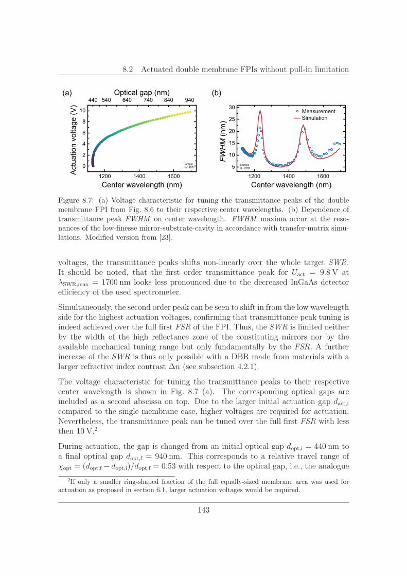
8.2 Actuated double membrane FPIs without pull-in limitation
1200 1400 1600
0
2
4
6
8
10
Actuationvoltage(V)
Center wavelength (nm)
440 540 640 740 840 940
SampleHu192B
Optical gap (nm)(a)
1200 1400 1600
5
10
15
20
25
30
FWHM(nm)
Center wavelength (nm)
MeasurementSimulation
SampleHu192B
(b)
Figure 8.7: (a) Voltage characteristic for tuning the transmittance peaks of the doublemembrane FPI from Fig. 8.6 to their respective center wavelengths. (b) Dependence oftransmittance peak FWHM on center wavelength. FWHM maxima occur at the reso-nances of the low-finesse mirror-substrate-cavity in accordance with transfer-matrix simu-lations. Modified version from [23].
voltages, the transmittance peaks shifts non-linearly over the whole target SWR.It should be noted, that the first order transmittance peak for U = . atλ , = looks less pronounced due to the decreased InGaAs detectorefficiency of the used spectrometer.
Simultaneously, the second order peak can be seen to shift in from the low wavelengthside for the highest actuation voltages, confirming that transmittance peak tuning isindeed achieved over the full first FSR of the FPI. Thus, the SWR is limited neitherby the width of the high reflectance zone of the constituting mirrors nor by theavailable mechanical tuning range but only fundamentally by the FSR. A furtherincrease of the SWR is thus only possible with a DBR made from materials with alarger refractive index contrast Δn (see subsection 4.2.1).
The voltage characteristic for tuning the transmittance peaks to their respectivecenter wavelength is shown in Fig. 8.7 (a). The corresponding optical gaps areincluded as a second abscissa on top. Due to the larger initial actuation gap d ,
compared to the single membrane case, higher voltages are required for actuation.Nevertheless, the transmittance peak can be tuned over the full first FSR with lessthen .2
During actuation, the gap is changed from an initial optical gap d , = toa final optical gap d , = . This corresponds to a relative travel range ofχ = (d , − d , )/d , = 0.53 with respect to the optical gap, i.e., the analogue
2If only a smaller ring-shaped fraction of the full equally-sized membrane area was used foractuation as proposed in section 6.1, larger actuation voltages would be required.
143
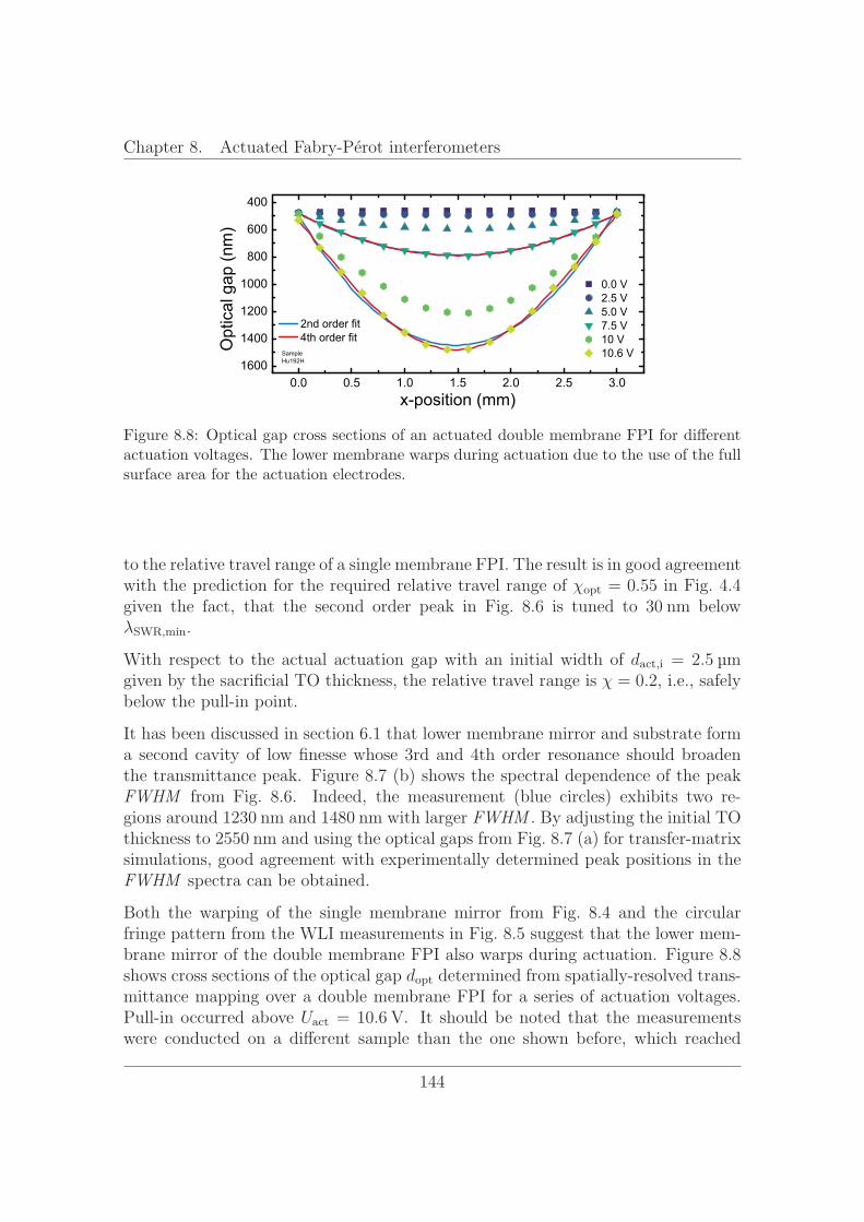
Chapter 8. Actuated Fabry-Perot interferometers
0.0 0.5 1.0 1.5 2.0 2.5 3.01600
1400
1200
1000
800
600
400
2nd order fit4th order fitO
pticalgap(nm)
x-position (mm)
0.0 V2.5 V5.0 V7.5 V10 V10.6 VSample
Hu192H
Figure 8.8: Optical gap cross sections of an actuated double membrane FPI for differentactuation voltages. The lower membrane warps during actuation due to the use of the fullsurface area for the actuation electrodes.
to the relative travel range of a single membrane FPI. The result is in good agreementwith the prediction for the required relative travel range of χ = 0.55 in Fig. 4.4given the fact, that the second order peak in Fig. 8.6 is tuned to belowλ , .
With respect to the actual actuation gap with an initial width of d , = .given by the sacrificial TO thickness, the relative travel range is χ = 0.2, i.e., safelybelow the pull-in point.
It has been discussed in section 6.1 that lower membrane mirror and substrate forma second cavity of low finesse whose 3rd and 4th order resonance should broadenthe transmittance peak. Figure 8.7 (b) shows the spectral dependence of the peakFWHM from Fig. 8.6. Indeed, the measurement (blue circles) exhibits two re-gions around and with larger FWHM . By adjusting the initial TOthickness to and using the optical gaps from Fig. 8.7 (a) for transfer-matrixsimulations, good agreement with experimentally determined peak positions in theFWHM spectra can be obtained.
Both the warping of the single membrane mirror from Fig. 8.4 and the circularfringe pattern from the WLI measurements in Fig. 8.5 suggest that the lower mem-brane mirror of the double membrane FPI also warps during actuation. Figure 8.8shows cross sections of the optical gap d determined from spatially-resolved trans-mittance mapping over a double membrane FPI for a series of actuation voltages.Pull-in occurred above U = . . It should be noted that the measurementswere conducted on a different sample than the one shown before, which reached
144
8.2 Actuated double membrane FPIs without pull-in limitation
higher deflections at a given voltage so that the second order peak position had tobe used to derive the optical gap d for several measurement points.
It can be seen that the optical gaps get increasingly inhomogeneous the further thelower membrane is deflected. Accordingly, for transmittance through the full aper-ture, resolution would strongly decrease towards the low wavelength range. Con-sequently, the current design without ring-shaped actuation electrode is suitable todemonstrate the increased tuning range which can be achieved with a double mem-brane approach but cannot provide a high resolution filter over the SWR which itcan in principle operate in.
Indeed, Fig. 8.8 shows an overall travel range of Δd = in the membranecenter which corresponds to a pull-in point of χ = 0.41. The pull-in point is inclose agreement with the one found for the single membrane case since the underlyingactuator geometry is the same. As stated above, the necessary travel range of χ = 0.2is therefore within a regime of safe device operation.
Furthermore, second and fourth order polynomial fits to two of the optical gap crosssections are depicted in Fig. 8.8. It has been argued in section 6.2 that the membraneprofile during actuation can be approximated by the quadratic profile of a membraneloaded by a constant pressure. The approximation is valid for the intermediate de-flection at U = . where the inverse relationship between attractive capacitiveforce and local actuation gap leads only to a slightly higher force in the membranecenter. For the highest deflection at U = . , on the other hand, only a fourthorder polynomial can fully reproduce the membrane profile, i.e., electrostatic pres-sure can no longer be regarded as constant. Nevertheless, within the travel rangeneeded for full first FSR tuning the quadratic approximation is sufficient.
Finally, it should be noted that the typical range of pull-in voltages (e.g., hereU = . ) found for these double membrane FPIs was lower than the roughlyestimated value of . from section 6.2. There are several possible reasons whichwould lead to a reduced U . First, the convex wafer bow due to the removedbackside TO (see Fig. 7.10) effectively reduces the initial actuation gap d , . Second,the thin μc-Si might reduce the residual stress of the mirror membrane. Last, it canbe expected that larger deflections in the membrane center close to the pull-in pointχ as evidenced above reduce the pull-in voltage U .
145
Chapter 8. Actuated Fabry-Perot interferometers
8.3 Summary: Double membrane FPIs for broad
spectral working ranges
Summing up, successfully actuated single and double membrane FPIs were demon-strated in this chapter. It was shown that pull-in occurs in the single membrane casewhile tuning the first order transmittance peak within its FSR, thereby ultimatelylimiting the usable SWR. For double membrane FPIs, however, transmittance peaktuning over the full first FSR without pull-in is possible because the initial actua-tion gap d , can be chosen independently of the initial optical gap d , . Despitethe larger actuation gap compared to single membrane FPIs, the required actuationvoltages are still in a range of for a membrane diameter of . Such voltagescan easily be provided in many applications.
Referring back to the overview of published SWRs in Fig. 4.2, it can be stated thatthe double membrane architecture enables an unprecedented SWR in the NIR for asurface-micromachined FPI with millimeter-sized aperture. While devices with com-parable aperture size from VTT/Spectral Engines have a SWR of − of theircenter wavelength [11, 43], the FPIs shown here achieve . Previously demon-strated surface-micromachined FPIs with such an SWR had significantly smalleraperture diameters below [108].
Drawbacks of the presented devices are the reduced gap homogeneity leading to a lossof resolution during actuation due to membrane warping under full-area actuationand a poor reliability of the electrical contacts. Accordingly, necessary next stepsare the implementation of a ring-shaped actuation electrode, metallic contacts anddedicated, insulated feed lines to the electrodes in order to benefit from the fullpotential of double membrane FPIs. All of these improvements are feasible usingthe PECVD SiCN/aSi-based technology presented within this thesis but will requireadditional lithography steps.
146
Chapter 9
Conclusion and outlook
This thesis focused on increasing the spectral working range (SWR) of surface-micromachined MEMS Fabry-Perot interferometers (FPIs) working in the near in-frared without sacrificing neither optical aperture area nor optical resolution. Tothat end, strategies for circumventing limitations in state-of-the-art FPIs were de-rived and their feasibility demonstrated by fabricating proof-of-principle devicescompatible with standard MEMS processes. Thereby, this work has led to newdevelopments both in the field of MEMS materials research and FPI device archi-tecture.
In order to increase the SWR, a MEMS concept had to be found where SWR isonly limited by the first free spectral range (FSR) rather than the width of the highreflectance zone of the FPI mirrors or the achievable travel range. As a part of asolution to this challenge, it was shown that distributed Bragg reflectors (DBRs)made from silicon and silicon carbonitride (SiCN) are an attractive choice. Thisis because SiCN can be deposited by plasma-enhanced chemical vapor deposition(PECVD) such that it fulfills several requirements simultaneously. First, its refrac-tive index contrast to silicon leads to high average reflectance of 0.96 throughoutthe full first FSR. Second, tuning of mechanical stress in the DBR to the tensileregime is possible via post-deposition annealing yielding an attractive means to con-trol the mechanical stress level independently from the optical properties. Moreover,the mirror is fully resistant towards sacrificial vapor HF etching. Thereby, Si/SiCNDBRs can be released as stable, flat mirror membranes by means of SiO2 sacrificiallayer etching.
Furthermore, a double membrane FPI structure was proposed which enables sep-arating the initial optical gap between the mirrors and the initial actuation gapbetween the actuation electrodes in order to circumvent pull-in limitation normally
147
Chapter 9. Conclusion and outlook
found in surface-micromachined FPIs. An additional benefit arises from the factthat both mirror membranes are decoupled from the substrate in the optical region.Accordingly, their parallelism remains unaffected by substrate curvature so that highoptical resolution can be maintained.
By fabricating tunable proof-of-principle double membrane FPIs with such Si/SiCNDBRs, successful integration of SiCN into a working MEMS device could be demon-strated. Despite the high aspect ratio of 1:10000 between a sacrificial optical gap ofaround and large membrane diameters of up to , FPIs could be releasedwithout stiction. Thanks to the double membrane structure, these devices exhibiteddeviations from both mirror flatness and mirror parallelism in the nanometer rangeonly. These deviations were independent of membrane diameter in the case whenno actuation voltage was applied. Given the optical transmittance performance interms of peak full width at half maximum (FWHM ) close to the ideal simulatedvalue below , such devices pave the way towards high-resolution and high-throughput optical filters. Furthermore, to the author’s best knowledge, the demon-strated tunable FPIs achieved the highest SWR for surface-micromachined FPIswith millimeter-sized apertures reported so far. To be precise, an SWR extendingfrom to ( of the center wavelength) was shown.
Starting from these results, modifications, which were not part of this thesis, such asa ring-shaped actuation electrode, substrate removal in the optical aperture area andimproved metallic contacts to the electrode layers can be included in the design forfuture devices. These should remedy current shortcomings of the proof-of-principledevices, namely membrane warping during actuation, a detrimental additional cavitybetween lower mirror and substrate and unreliable electrical contacts. In sum, theyenable high resolution during actuation over the full first FSR.
From a methodology point of view, spatially-resolved transmittance measurementson large-area filters were introduced in this thesis. As the spatial optical gap profileof an FPI can be deduced from such measurements, they gave deeper insight intothe causes for a low geometric defect finesse compared to conventional full aperturetransmittance measurements. Thus, the detrimental influence of the substrate waferbow in single membrane FPIs could be identified as a dominant limiting mechanismfor their performance.
It should be noted that the results shown in this thesis can be applied beyondSi/SiCN FPIs. The general properties of SiCN such as HF resistance, tunable stress,low conductance and compatibility with existing processing equipment, to name justa few, form a unique set which cannot be found in a standard MEMS materialsportfolio. It can therefore be expected that other MEMS applications could benefitfrom SiCN, e.g., as an HF resistant passivation layer. To that end, a deeper study
148
which also exploits the effect of the remaining PECVD deposition parameters onthe relevant properties for MEMS fabrication can be useful.
Furthermore, the double membrane design is likely to have more advantages thenthose covered here. As an example, when moving from chip-level to fully packageddevices, double membrane FPIs should be more robust towards coupling to externalstress by virtue of their design. Thereby, device packaging cost can potentially bereduced while high resolution is preserved.
Obviously, double membrane FPI concepts are not restricted to Si/SiCN mirrors butcan increase the SWR whenever the achievable tuning range is limited by electro-static pull-in. Indeed, coworkers of the author have recently successfully fabricateddouble membrane FPIs with three layer Si/air DBRs (another beneficial materialcombination) which do incorporate a backside trench and a ring-shaped actuationelectrode [236]. Thereby, these devices maintain their high resolution during tuningof their first order transmittance peak over a range from to .
In the future, when combined with a detector, such a double membrane FPI forms alow-cost miniaturized spectrometer which can detect spectral fingerprints within afull overtone order thanks to its uniquely broad SWR. Accordingly, manifold spec-troscopic applications can be addressed by a single device. Due to its small size andcost, such a miniaturized spectrometer could be integrated in everyday consumerelectronic products extending their sensing capabilities and thus placing the powerof spectroscopic material analysis into the hands of everyone.
149

Chapter 9. Conclusion and outlook
150
Appendix A
List of equipment and processes
Fabrication
HF release
HF release processes were performed in a MEMSStar ORBIS ALPHA etch tool at◦ pedestal temperature. The system uses vaporized deionized water as a catalyst
for the etch process with anhydrous HF vapor. This chemistry allows for a higherselectivity between silicon oxide and silicon nitride than conventional alcohol catalystbased systems [237]. Control of the etch speed is mainly achieved by variationof process pressure and water catalyst supply rate. Higher pressures increase theresidence time of adsorbed HF and water vapor at the etch front and thereby increasethe etch rate [224].
Plasma-enhanced chemical vapor deposition
PECVD of SiCN, silicon (both in amorphous and microcrystalline form) and TEOSoxide were conducted in a PlasmaLab 100 chamber from Oxford Instruments PlasmaTechnology. Plasma is excited capacitively in a parallel plate configuration betweena gas showerhead and the substrate table with either . radio frequency or
. Precursor gases SiH4, CH4 and NH3, doping gases PH3 and B2H6 (bothdiluted in H2) as well as dilution gases Ar and H2 are provided via separate gasinlets and mixed in the showerhead. TEOS is stored in a bubbler with Ar as thecarrier gas which is then combined with O2 from a separate gas line in order toreduce hazards from mixing with SiH4.
151
Chapter A. List of equipment and processes
For SiCN depositions a flow rate ratio of SiH4:CH4:NH3:Ar=4:25:5:250 was used ata radio frequency power of and chamber pressure. Apart from thetemperature experiments in chapter 5 all depositions took place at ◦ substrateheater temperature.
Amorphous silicon was deposited from SiH4 and Ar at 1:19 flow rate ratio,plasma power at at the same temperature as SiCN in order to be able todeposit full mirrors consecutively.
Microcrystalline silicon was deposited with H2 instead of Ar as a dilution gas at astrong hydrogen dilution of 600 and a plasma power of . Doped layers weredeposited by adding diborane diluted in hydrogen to the gas mixture.
TEOS was deposited at a fixed carrier gas flow using a low frequency plasma,. and ◦ .
The chamber was pumped down to a pressure below − before depositionand the wafer was allowed to heat up for approximately one minute.
RIE
Anisotropic etching of silicon, SiCN and TEOS oxide was performed with the custom-made inductively coupled plasma custom etch tool, at which the Bosch process hasbeen developed over 20 years ago [214, 238]. A mixture of SF6, C4F8 and O2 hasbeen used to etch through both silicon and SiCN in the DBRs in a single process.Oxide etching has been conducted on the basis of CF4 gas.
Characterization
IR Absorption
A Bruker Vertex v80 FTIR spectrometer with a measurement range from −
to − and a resolution of − was used in transmission mode to determinethe IR absorption coefficient of SiCN thin-films. To that end, double sided polishedsilicon wafers were always used as a substrate and reference measurements weretaken with an uncoated wafer in the light path. In order to suppress unwanted ab-sorption from water and CO2 vapor, the chamber was evacuated down to a pressureof . .
Transmittance spectra had to be converted to absorption coefficient spectra to be
152
able to quantitatively compare spectra taken from films of different thickness. In thecase of thin-films, this process is more complicated due to thin-film interference thanin the case of IR absorption in a gas as conversion cannot simply be done by meansof Lambert-Beers law [167, 170, 239]. The iterative solution approach proposed byKing and Milosevic [207,240] has been used in this thesis because it takes thin-filminterference into account, gives a Kramers–Kronig consistent result and does not re-quire a priori assumptions about the absorption coefficient. Thickness and refractiveindex (real part) values from ellipsometry have been used as starting values in theiterative process. It has to be noted that the final result which the method convergesto does depend on the initial choice of starting values. It was therefore checked afterconvergence that the resulting fit variables (thickness, complex refractive index) leadto a good fit of the measured transmittance spectra.
Laser Doppler vibrometry
A Polytec MSA-100-3D micro system analyzer was used to measure vibrationalspectra of released mirror membranes. Exploiting the Doppler frequency shift whena probe laser is reflected at a moving object, vibrations can be resolved with sub-picometer resolution by analyzing the beat frequency after the probe beam has beencombined with a reference beam. The device works with a bandwidth ofand can measure vibrations in all three dimensions even though only out-of-planemovement was measured here. In order to excite vibrations, samples were gluedto a ceramic piezoelectric shaker plate which was driven by periodic chirps with
amplitude. In order to reduce squeeze film damping, the sample was thenplaced in a vacuum box which was evacuated down to a range of pressures betweenp = and p = .
Spectroscopic ellipsometry
Spectroscopic ellipsometry was used for measuring the refractive index of SiCN aswell as for determining thin-film thicknesses both for individual films and in completethin-film stacks. Measurements were performed with a Sentech SE800 spectroscopicellipsometer with a measurement range from to equipped with agoniometer for variable angle measurements. For refractive index measurements,spectra were generally taken over the full spectral range at ◦, ◦ and ◦ in orderto provide the maximum possible information for later fitting of model functions.For film thickness measurements with relatively well known refractive index, singleangle measurements at ◦ were used with the spectral range sometimes limited toa range from to .
153
Chapter A. List of equipment and processes
Fitting of the resulting spectra for the ellipsometric angles Ψ and Δ was conductedusing parameterized model functions for the refractive indices. Silicon oxides weremodelled as a simple Cauchy model. The Tauc-Lorentz model for amorphous semi-conductors [182, 183] was used for amorphous silicon and amorphous SiCN bothof which had their optical band gap E within the measurement range. Furtherinformation on the resulting models are given in Appendix C.
Stylus profilometry
A DektakXT stylus profilometer was used to measure step heights and membranesurface profiles. Measurements of up to length (i.e. larger than membranediameters used in this work) can be performed in a single scan with a verticalresolution of .
UV-VIS-NIR reflectance/transmittance
Reflectance and transmittance measurements in the UV-VIS-NIR range were con-ducted on a Cary 5000 spectrophotometer which was equipped with a universalmeasurement accessory. This allows for adjusting both the angle of incidence onthe sample and the angle of detection independently without the need to manuallymove the sample between measurements. Measurements can be taken in s- andp-polarization separately using polarization filters.
Such measurements were used to characterize the reflectance of deposited mirrors.Furthermore, the extinction coefficient of SiCN in subsection 5.2.3 was determinedfrom reflectance and transmittance measurements in p-polarization at ◦ and ◦
using the TRACK method [188].
Wafer curvature
Measurement of wafer curvature was done with a KLA Tencor FLX-2908 using thedeflection of a laser beam from a curved substrate. From such curvature measure-ments before and after deposition of a thin-film, the mechanical stress in the filmcan be calculated by means of the Stoney equation (see Eq. 4.1) if film and substratethickness as well as the substrate’s biaxial modulus are known.
The device is capable of performing in-situ wafer curvature measurements duringannealing at temperatures up to ◦ while purging the sample chamber withnitrogen in order to prevent oxidation of the thin-films at elevated temperatures.
154
White light interferometry
A Zygo NewView5030 white light interferometer was used to measure surface profilesof released membranes. It is equipped with a series of interferometric objectivesof different magnification, a 640x480 pixel camera and a motorized tip-tilt stage.Measurements are performed by a vertical scan of the objective which causes thezero retardation fringe of the resulting interference pattern on the camera to sweepover the image. The z-position of the fringe corresponds to a map of the surfaceprofile. Vertical resolution is up to .
XPS
XPS measurement were conducted on a PHI Quantera photoelectron spectrometerusing the aluminum Kα-line
1. It is equipped with an Ar ion source for sputteringdepth profiles. Measurements comprised a scan over the full available energy rangein order to determine all elements at the surface. For the depth profiles the spectralrange was limited to the respective elements which had been found on the surfacebefore. In order to exclude that other elements are present within the thin-film, thespectrum at the final sputter depth was again recorded over the full range.
1The author thanks Dr. Anne Fuchs from the Robert Bosch GmbH analytics department forthe measurements.
155

Chapter A. List of equipment and processes
156
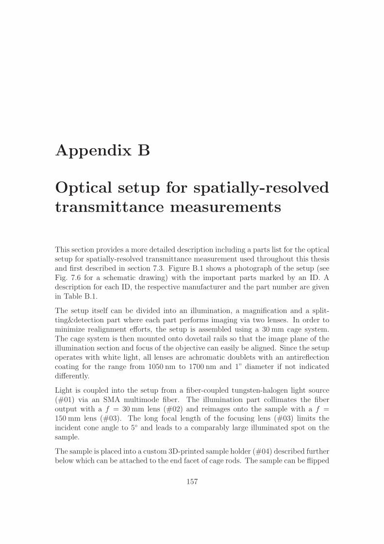
Appendix B
Optical setup for spatially-resolvedtransmittance measurements
This section provides a more detailed description including a parts list for the opticalsetup for spatially-resolved transmittance measurement used throughout this thesisand first described in section 7.3. Figure B.1 shows a photograph of the setup (seeFig. 7.6 for a schematic drawing) with the important parts marked by an ID. Adescription for each ID, the respective manufacturer and the part number are givenin Table B.1.
The setup itself can be divided into an illumination, a magnification and a split-ting&detection part where each part performs imaging via two lenses. In order tominimize realignment efforts, the setup is assembled using a cage system.The cage system is then mounted onto dovetail rails so that the image plane of theillumination section and focus of the objective can easily be aligned. Since the setupoperates with white light, all lenses are achromatic doublets with an antireflectioncoating for the range from to and 1” diameter if not indicateddifferently.
Light is coupled into the setup from a fiber-coupled tungsten-halogen light source(#01) via an SMA multimode fiber. The illumination part collimates the fiberoutput with a f = lens (#02) and reimages onto the sample with a f =
lens (#03). The long focal length of the focusing lens (#03) limits theincident cone angle to ◦ and leads to a comparably large illuminated spot on thesample.
The sample is placed into a custom 3D-printed sample holder (#04) described furtherbelow which can be attached to the end facet of cage rods. The sample can be flipped
157
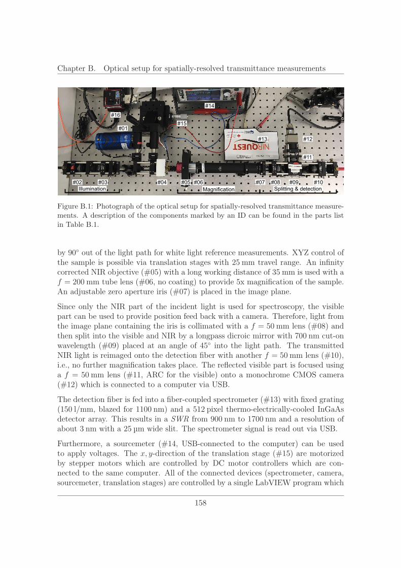
Chapter B. Optical setup for spatially-resolved transmittance measurements
#01
#02 #03 #04 #05 #06 #07 #08 #09 #10
#11
#12#13
#14
#15#16
Illumination Magnification Splitting & detection
Figure B.1: Photograph of the optical setup for spatially-resolved transmittance measure-ments. A description of the components marked by an ID can be found in the parts listin Table B.1.
by ◦ out of the light path for white light reference measurements. XYZ control ofthe sample is possible via translation stages with travel range. An infinitycorrected NIR objective (#05) with a long working distance of is used with af = tube lens (#06, no coating) to provide 5x magnification of the sample.An adjustable zero aperture iris (#07) is placed in the image plane.
Since only the NIR part of the incident light is used for spectroscopy, the visiblepart can be used to provide position feed back with a camera. Therefore, light fromthe image plane containing the iris is collimated with a f = lens (#08) andthen split into the visible and NIR by a longpass dicroic mirror with cut-onwavelength (#09) placed at an angle of ◦ into the light path. The transmittedNIR light is reimaged onto the detection fiber with another f = lens (#10),i.e., no further magnification takes place. The reflected visible part is focused usinga f = lens (#11, ARC for the visible) onto a monochrome CMOS camera(#12) which is connected to a computer via USB.
The detection fiber is fed into a fiber-coupled spectrometer (#13) with fixed grating( / , blazed for ) and a thermo-electrically-cooled InGaAsdetector array. This results in a SWR from to and a resolution ofabout with a wide slit. The spectrometer signal is read out via USB.
Furthermore, a sourcemeter (#14, USB-connected to the computer) can be usedto apply voltages. The x, y-direction of the translation stage (#15) are motorizedby stepper motors which are controlled by DC motor controllers which are con-nected to the same computer. All of the connected devices (spectrometer, camera,sourcemeter, translation stages) are controlled by a single LabVIEW program which
158
Table B.1: Part list for the spatially-resolved transmittance setup.
ID Description Manufacturer Part No.
#01 Tungsten-halogen light source Ocean Optics HL-2000-FSHA#02 f = achromat doublet Thorlabs AC254-030-C-ML#03 f = achromat doublet Thorlabs AC254-150-C-ML#04 Custom sample holder - -#05 5x NIR microscope objective Mitutoyo M Plan APO NIR 5x#06 f = tube lens Mitutoyo MT-4#07 Zero aperture iris Thorlabs SM1D12CZ#08 f = achromat doublet Thorlabs AC254-050-C-ML#09 Dicroic longpass Edmund optics #69-903#10 f = achromat doublet Thorlabs AC254-050-C-ML#11 f = achromat doublet Thorlabs AC254-050-B-ML#12 USB monochrome camera IDS GmbH UI-3160CP-M-GL#13 Spectrometer Ocean Optics NIRQuest512#14 Sourcemeter Tektronix Keithley 2450#15 XYZ translation stage Thorlabs PT3/M#16 Brushed DC Servo controller Thorlabs KDC101
allows automated measurements to be taken at arbitrary combinations of actuationvoltages and measurement positions [234].
It should be noted that despite silicon absorption of the visible part when a waferis placed in the light path, the transmitted light is sufficient for the camera image.The latter in conjunction with the adjustable iris provides orientation on the samplein x, y-direction and helps to bring the sample into focus properly.
The size of the measurement spot is mainly limited by the diameter of the detectionfiber ( ) and only reduced by the iris if it is almost fully closed. In the ideal caseof perfect alignment without aberrations, the fiber core size leads to a spotsize of diameter due to the magnification by a factor of five. In practice, sincealignment and focusing is done using visible white light and the objective numericalaperture is small (NA= 0.14) due to its long working distance (WD= ) theactual spot size is larger. Experimentally, the spot size has been determined to beroughly in diameter.
Full area transmittance measurements were conducted with a simpler setup usingthe same light source and spectrometer. The sample was placed between two fibercollimators for the excitation and the detection fiber. The size of the measurementspot was limited before and after the sample by two adjustable irises.
159
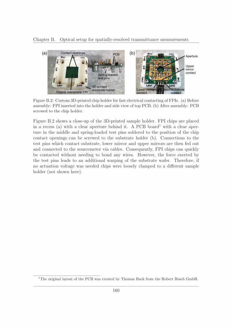
Chapter B. Optical setup for spatially-resolved transmittance measurements
(a) (b)
Spring-loadedtest pins
3D-printedsubstrate holder
Contact openings PCB
Lower mirrorcontact
Substratecontact
Uppermirrorcontact
Aperture
Double membrane FPI
Figure B.2: Custom 3D-printed chip holder for fast electrical contacting of FPIs. (a) Beforeassembly: FPI inserted into the holder and side view of top PCB. (b) After assembly: PCBscrewed to the chip holder.
Figure B.2 shows a close-up of the 3D-printed sample holder. FPI chips are placedin a recess (a) with a clear aperture behind it. A PCB board1 with a clear aper-ture in the middle and spring-loaded test pins soldered to the position of the chipcontact openings can be screwed to the substrate holder (b). Connections to thetest pins which contact substrate, lower mirror and upper mirrors are then fed outand connected to the sourcemeter via cables. Consequently, FPI chips can quicklybe contacted without needing to bond any wires. However, the force exerted bythe test pins leads to an additional warping of the substrate wafer. Therefore, ifno actuation voltage was needed chips were loosely clamped to a different sampleholder (not shown here).
1The original layout of the PCB was created by Thomas Buck from the Robert Bosch GmbH.
160
Appendix C
Refractive index data for opticalsimulations
The following refractive index models or tabulated values for have been used for theoptical simulations
Crystalline silicon
Tabulated data which consist of the well-known values of Jellison [241] in the visiblewhich were continued up to . in-house by SENTECH Instruments GmbH wereused.
Amorphous silicon
Values were determined from a-Si deposited on an SiO2 spacer layer by variable-angle SE. Fitting resulted in a Tauc-Lorentz model with the following parameters(see Eq. 5.1): E = . , β = . , E0 = . , γ = .
Amorphous silicon carbonitride
Values were determined by variable-angle SE from single layers of SiCN depositedon a silicon wafer. Fitting resulted in the following Tauc-Lorentz parameters:E = . , β = , E0 = . , γ = .
161

Chapter C. Refractive index data for optical simulations
Silicon oxide
Since SiO2 is transparent in the spectral range of interest it was modeled as a Cauchylayer by the following formula: n = 1.452 + ·λ−2
162
Appendix D
Pull-in for actuation of membraneswith generalized ring electrodes
In the following, a formalism for predicting the pull-in point χ and pull-in voltageU for a circular membrane actuated by a ring-shaped electrode will be presented.The theory is applicable to all FPI designs discussed in this thesis, since the fabri-cated devices with full area actuation represent a special case, namely for the innerelectrode ring radius r = 0 and the outer ring radius r = r being equal to themembrane radius r . The idea is built on the generalized theory presented in [242]which has been adapted to circular membranes1.
The total coenergy in a capacitor with arbitrary geometry where one of the electrodesis suspended by a spring so that it can be displaced with a single degree of freedom(see Fig. D.1 (a)) is [242]
E (χ) = E (χ)− E (χ) =1
2C (χ)U2 − E (χ). (D.1)
Here, E (χ) and E (χ) are the energy stored in capacitor and spring, respec-tively, χ is a generalized coordinate which describes the displacement and C (χ) isthe capacitance for a given displacement. For this discussion χ can be chosen asthe center displacement Δd of the movable membrane normalized to the initialactuation gap d , , i.e., χ = Δd
d ,. In the case of a Hookean spring with spring
constant k, this results in
E (χ) =1
2kd2 , χ
2. (D.2)
1The author acknowledges cooperation with Dr. Christoph Krammer from the Robert BoschGmbH.
163
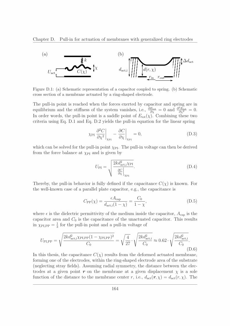
Chapter D. Pull-in for actuation of membranes with generalized ring electrodes
k
Uχ
C(χ)r r
Δd
d , d(r, χ)
(a) (b)
Figure D.1: (a) Schematic representation of a capacitor coupled to spring. (b) Schematiccross section of a membrane actuated by a ring-shaped electrode.
The pull-in point is reached when the forces exerted by capacitor and spring are inequilibrium and the stiffness of the system vanishes, i.e., ∂E
∂χ= 0 and ∂2E
∂χ2 = 0.
In order words, the pull-in point is a saddle point of E (χ). Combining these twocriteria using Eq. D.1 and Eq. D.2 yields the pull-in equation for the linear spring
χ∂2C
∂χ2
∣∣∣∣χ
− ∂C
∂χ
∣∣∣∣χ
= 0, (D.3)
which can be solved for the pull-in point χ . The pull-in voltage can then be derivedfrom the force balance at χ and is given by
U =
√√√√2kd2 , χ
∂C∂χ
∣∣∣χ
. (D.4)
Thereby, the pull-in behavior is fully defined if the capacitance C(χ) is known. Forthe well-known case of a parallel plate capacitor, e.g., the capacitance is
C (χ) =εA
d , (1− χ)=
C0
1− χ, (D.5)
where ε is the dielectric permittivity of the medium inside the capacitor, A is thecapacitor area and C0 is the capacitance of the unactuated capacitor. This resultsin χ , = 1
3for the pull-in point and a pull-in voltage of
U , =
√2kd2 , χ , (1− χ , )2
C0
=
√4
27·
√2kd2 ,
C0
≈ 0.62 ·
√2kd2 ,
C0
.
(D.6)In this thesis, the capacitance C(χ) results from the deformed actuated membrane,forming one of the electrodes, within the ring-shaped electrode area of the substrate(neglecting stray fields). Assuming radial symmetry, the distance between the elec-trodes at a given point r on the membrane at a given displacement χ is a solefunction of the distance to the membrane center r, i.e., d (r, χ) = d (r, χ). The
164
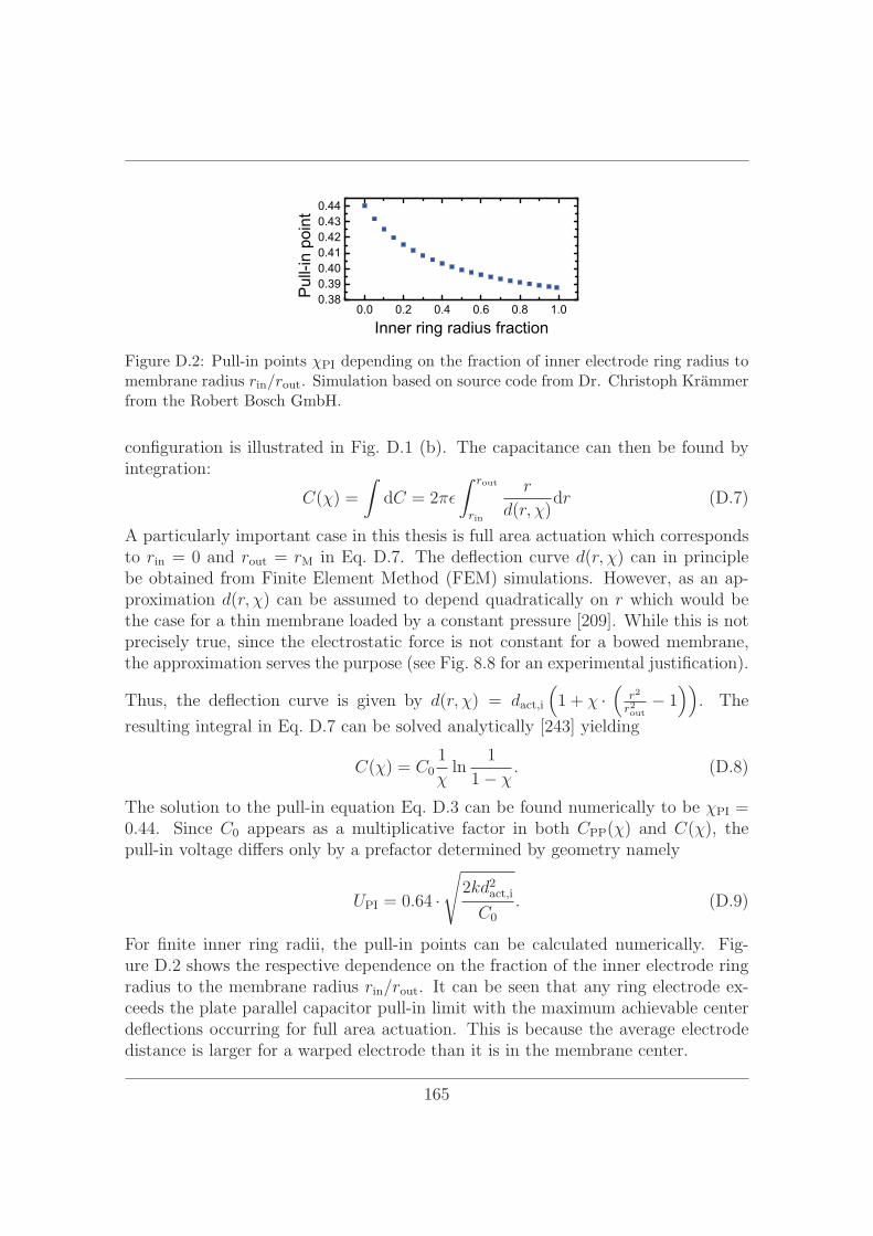
0.0 0.2 0.4 0.6 0.8 1.00.380.390.400.410.420.430.44
Pull-inpoint
Inner ring radius fraction
Figure D.2: Pull-in points χ depending on the fraction of inner electrode ring radius tomembrane radius r /r . Simulation based on source code from Dr. Christoph Krammerfrom the Robert Bosch GmbH.
configuration is illustrated in Fig. D.1 (b). The capacitance can then be found byintegration:
C(χ) =
∫dC = 2πε
∫ r
r
r
d(r, χ)dr (D.7)
A particularly important case in this thesis is full area actuation which correspondsto r = 0 and r = r in Eq. D.7. The deflection curve d(r, χ) can in principlebe obtained from Finite Element Method (FEM) simulations. However, as an ap-proximation d(r, χ) can be assumed to depend quadratically on r which would bethe case for a thin membrane loaded by a constant pressure [209]. While this is notprecisely true, since the electrostatic force is not constant for a bowed membrane,the approximation serves the purpose (see Fig. 8.8 for an experimental justification).
Thus, the deflection curve is given by d(r, χ) = d ,
(1 + χ ·
(r2
r2− 1
)). The
resulting integral in Eq. D.7 can be solved analytically [243] yielding
C(χ) = C01
χ
1
1− χ. (D.8)
The solution to the pull-in equation Eq. D.3 can be found numerically to be χ =0.44. Since C0 appears as a multiplicative factor in both C (χ) and C(χ), thepull-in voltage differs only by a prefactor determined by geometry namely
U = 0.64 ·
√2kd2 ,
C0
. (D.9)
For finite inner ring radii, the pull-in points can be calculated numerically. Fig-ure D.2 shows the respective dependence on the fraction of the inner electrode ringradius to the membrane radius r /r . It can be seen that any ring electrode ex-ceeds the plate parallel capacitor pull-in limit with the maximum achievable centerdeflections occurring for full area actuation. This is because the average electrodedistance is larger for a warped electrode than it is in the membrane center.
165

———————–
List of publications
Regular articles
1. MEMS Fabry-Perot interferometers with double membrane mirrorsfor improved mirror parallelism,C. Huber, P. Liu, C. Krammer, B. Stein, and H. Kalt, J. Microelectromech.Sys. 27, 836-843 (2018)
2. Plasma-enhanced chemical vapor deposition of amorphous siliconcarbonitride: Deposition temperature dependence of bonding struc-ture, refractive index, mechanical stress and their aging under am-bient air,C. Huber, B. Stein, and H. Kalt, Thin Solid Films 634, 66-72 (2017)
3. Luminescence properties of Cu2ZnSn(S,Se)4 solar cell absorbers: Statefilling versus screening of electrostatic potential fluctuations,M. Lang, C. Zimmermann, C. Krammer, T. Renz, C. Huber, H. Kalt, and M.Hetterich, Phys. Rev. B 95, 155202 (2017)
4. Diffuse electroreflectance of thin-film solar cells: Suppression ofinterference-related lineshape distortions,C. Krammer, C. Huber, A. Redinger, D. Sperber, G. Rey, S. Siebentritt, H.Kalt, and M. Hetterich, Appl. Phys. Lett. 107, 222104 (2015)
5. Electroreflectance of thin-film solar cells: Simulation and experi-ment,C. Huber, C. Krammer, D. Sperber, A. Magin, H. Kalt, and M. Hetterich,Phys. Rev. B 92, 075201 (2015)
6. Reversible order-disorder related band gap changes inCu2ZnSn(S,Se)4 via post-annealing of solar cells measured by elec-troreflectance,C. Krammer, C. Huber, C. Zimmermann, M. Lang, T. Schnabel, T. Abzieher,E. Ahlswede, H. Kalt, and M. Hetterich, Appl. Phys. Lett. 105, 262104 (2014)
167
List of publications
Contributions to international conferences
1. Tunable double membrane MEMS Fabry-Perot interferometers forthe near-infrared,C. Huber, C. Krammer, B. Stein, and H. Kalt, IEEE Conference on OpticalMEMS and Nanophotonics, Lausanne, Switzerland (2018), Talk
2. Large-aperture Fabry-Perot filters based on silicon/silicon carboni-tride distributed Bragg reflectors for the near-infrared,C. Huber, B. Stein, and H. Kalt, IEEE Sensors Conference, Glasgow, UnitedKingdom (2017), Talk
3. Band gap changes of the CdS buffer induced by post-annealing ofCu2ZnSn(S,Se)4 solar cells,M. Lang, N. Schafer, C. Huber, T. Schnabel, H. Kalt, and M. Hetterich, IEEEPhotovoltaic Specialists Conference, Washington D.C., District of Columbia,USA (2017), Talk
4. Amorphous hydrogenated silicon carbonitride as low refractive in-dex material in optical MEMS applications,C. Huber, B. Stein, and H. Kalt, The European Conference on Lasers andElectro-optics (CLEO Europe), Munich, Germany (2017), Poster presentation
5. Refractive index and mechanical stress analysis of low-temperaturePECVD silicon-carbo-nitride,C. Huber, B. Stein, and H. Kalt, European Materials Research Society Fallmeeting, Warsaw, Poland (2016), Talk
6. The Influence of the degree of Cu–Zn disorder on the radiative re-combination transitions in Cu2ZnSn(S,Se)4 solar cells,M. Lang, C. Zimmermann, C. Krammer, C. Huber, T. Schnabel, T. Abzieher,E. Ahlswede, H. Kalt, and M. Hetterich, IEEE Photovoltaics Specialists Con-ference, New Orleans, Louisiana, USA (2015), Poster presentation
7. Order-disorder related band gap changes in Cu2ZnSn(S,Se)4: Impacton solar cell performance,C. Krammer, C. Huber, T. Schnabel, C. Zimmermann, M. Lang, E. Ahlswede,H. Kalt, and M. Hetterich, IEEE Photovoltaic Specialists Conference, NewOrleans, Louisiana, USA (2015), Poster presentation
Additionally, the author has contributed to more than 15 patent applications which,however, have not been laid open yet.
168

Abbreviations and symbols
Abbreviations
a-Si amorphous silicon
ALD atomic layer deposition
ARC antireflection coating
BOE buffered oxide etch
CMOS complementary metal oxide semiconductor
CTE coefficient of thermal expansion
CVD chemical vapor deposition
DBR distributed Bragg reflector
DFT density functional theory
DLP digital light projector
FEM finite element method
FIB focused ion beam
FPI Fabry-Perot interferometer
FSR free spectral range
FT Fourier transform
FTIR Fourier transform infrared
FWHM full width at half maximum
H high refractive index material
169

Abbreviations and symbols
HF hydrofluoric acid
HSI hyperspectral imaging
IR infrared
L low refractive index material
LDV Laser Doppler vibrometry
LPCVD low-pressure chemical vapor deposition
LVF linear variable filter
MEMS microelectromechanical system
MIR mid infrared
MOEMS microoptoelectromechanical system
μc-Si microcrystalline silicon
NA numerical aperture
NIR near infrared
OPD optical path difference
PECVD plasma-enhanced chemical vapor deposition
PVD physical vapor deposition
QED quantum electrodynamics
QWOT quarter-wave optical thickness
RIE reactive ion etching
SE spectroscopic ellipsometry
SEM scanning electron microscopy
SiCN silicon carbonitride
SiOCN silicon oxycarbonitride
SiRiN silicon-rich nitride
SNR signal-to-noise-ratio
SWG subwavelength grating
SWR spectral working range
170

SWIR short wave infrared
TEOS tetraethyl orthosilicate
TIR thermal infrared
TO thermal oxide
UV ultraviolet
VIS visible
WD working distance
WLI white light interferometry
XPS X-ray photoelectron spectroscopy
Symbols
In many cases throughout this thesis, indices are added to the symbols listed below inorder to specify their meaning. A separate list of these indices is provided thereafter.Indices are also used to refer a quantity to a chemical element so that n stands forrefractive index and n stands for the refractive index of silicon. Nevertheless, someof the quantities which are of special importance in this thesis are also explicitlystated in the following list.
Latin symbols
A area
b defect-specific factor in a defect finesse
B(ν) incident spectral intensity distribution
C Fringe contrast
d thickness of a layer
d actuation gap
d optical gap of an FPI
E energy
E band gap of a semiconductor
171

Abbreviations and symbols
E0 transition energy of a Lorentz oscillator
f focal length
f ,(m,n) resonance frequency of a mechanical oscillator
F coefficient of reflective finesse
F reflective finesse
F defect finesse
F divergence finesse
F effective finesse
G(φ) phase distribution of an FPI defect
h Planck’s constant
Hn(x) Hermite polynomial of order n
i unit imaginary number
j integer counter variable
Jm m-th order Bessel function of the first kind
Ii(νi) discrete measured intensity at wavenumber νi
k spring constant
K force
L(ν, ν ′) bandpass filter characteristic with its passband centered at ν ′
m interference order; order of Bessel functions
M electric dipole moment operator
n real part of the refractive index; order of Hermite polynomials
n complex refractive index
Δn refractive index contrast
N number of HL layer pairs in a DBR
p pressure
r radial polar coordinate
r position vector
172
r radius of curvature
R (intensity) reflectance at an interface or thin-film stack
s standard deviation
S(ν) spectral sensitivity of a photodetector
t time
t integration time
T (intensity) transmittance at an interface or thin-film stack
T transmittance through the full aperture area of a real FPI
T (intensity) transmittance through an FPI
T (ν, ξ) sensing matrix of the spectral element in a spectrometer
u out-of-plane deflection of a vibrating membrane
U actuation voltage
V volume
W linear coefficient in Taylor expansion of φ (ν)
x general Cartesian coordinate
y general Cartesian coordinate
Y Young modulus of a substrate
z height coordinate of a surface profile
Greek symbols
αm,n n-th root of the m-th order Bessel function of the first kind
β amplitude of a Lorentz oscillator
γ broadening parameter of a Lorentz oscillator
Γ→ transition rate from initial state i to final state f
δ optical path difference between to beams in a two-beam interferometer
Δ ellipsometric angle Δ
ε complex dielectric function
173
Abbreviations and symbols
ζ abbreviation in Stoney Equation, ζ = Y d2 /6d
θ angle of incidence w.r.t. surface normal
ϑ deposition temperature
λ wavelength
λ design wavelength of a DBR
Δλ width of DBR’s high reflectance zone in wavelength space
μ Poisson ratio of a substrate
ν optical frequency
ν wavenumber
ξ variable that a spectral element in a spectrometer uses for modulation
π pi
ρ density
σ mechanical stress
σ average mechanical stress
Δσ biaxial mechanical stress mismatch
ϕ polar angle
φ optical phase acquired during one round trip in an FPI
φ phase shift upon reflectance at an interface or thin-film stack
φ optical phase acquired by light propagation
Δφ width of a DBR’s high reflectance zone in phase space
χ relative displacement w.r.t. initial actuation gap Δd /d ,
χ pull-in point
ψ wavefunction
Ψ ellipsometric angle Ψ
174

Indices
act actuation
avg average
A referring to mirror A
b bow
B referring to mirror B
cap capacitor
capil capillary
cav cavity
D design
det detector
div divergence
f final
geo geometric
H referring to the high refractive index material
i initial
in inner
int integration
L referring to the low refractive index material
M mirror
max maximum
mech mechanical
min minimum
opt optical
out outer
PI pull-in
PP parallel plate
175

Abbreviations and symbols
prop propagation
r roughness
sub substrate
t tilt
tot total
TL Tauc-Lorentz
176
Bibliography
[1] R. Bogue, “Recent developments in MEMS sensors: a review of applications,markets and technologies,” Sensor Rev. 33, 300–304 (2013).
[2] Yole Developpement, Status of the MEMS industry 2018 - MEMS strike back!(2018).
[3] M. E. Motamedi, MOEMS: micro-opto-electro-mechanical systems, vol. 126(SPIE press, 2005).
[4] R. A. Crocombe, “Miniature optical spectrometers, part III: conventional andlaboratory near-infrared spectrometers,” Spectroscopy (2008).
[5] K. Keraenen, P. Karioja, O. Rusanen, J. Tenhunen, M. Blomberg, andA. Lehto, “Electrically tunable NIR spectrometer,” Proc. SPIE 3099, 181–184 (1997).
[6] R. A. Crocombe, “Handheld spectrometers in 2018 and beyond: MOEMS,photonics, and smartphones,” Proc. SPIE 10545, 10545 – 10545 – 12 (2018).
[7] M. Pollitt, “Boldly going where no mass spectrometer has gone before,” TheGuardian (2007). Accessed on August 28th, 2018.
[8] ams AG, AS7265x - Mobile Tricorder Color and NIR sens-ing demonstration (2017). Accessed on August 28th, 2018 athttps://www.youtube.com/watch?v=y6ccmh24BXw.
[9] P. Beuth, “Diese App macht das Smartphone zum Spektrometer,” DIE ZEIT(2017). Accessed on August 28th, 2018.
[10] Consumer Physics, Press release: Consumer Physics launches SCiO to demys-tify our material world (2014). Accessed on August, 20th 2018.
[11] Spectral Engines Oy, NIRONE Sensor product brochure (2018). Accessed onJune, 14th 2018.
177
BIBLIOGRAPHY
[12] P. Reinig, H. Gruger, J. Knobbe, T. Pugner, and S. Meyer, “Bringing NIRspectrometers into mobile phones,” Proc. SPIE 10545 (2018).
[13] A. Othman, H. Kotb, Y. Sabry, and D. Khalil, “MEMS-based Fourier trans-form spectrometer using pulsed infrared light source,” Proc. SPIE 10545(2018).
[14] L. P. Schuler, J. S. Milne, J. M. Dell, and L. Faraone, “MEMS-based mi-crospectrometer technologies for NIR and MIR wavelengths,” J. Phys. D 42,133001 (2009).
[15] J. Antila, M. Tuohiniemi, A. Rissanen, U. Kantojarvi, M. Lahti, K. Vi-herkanto, M. Kaarre, and J. Malinen, MEMS- and MOEMS-Based Near-Infrared Spectrometers (John Wiley & Sons, Ltd, 2013).
[16] J. Antila, U. Kantojarvi, J. Makynen, M. Tammi, and J. Suhonen, “AdvancedMEMS spectral sensor for the NIR,” Proc. SPIE 9375 (2015).
[17] C. Huber, B. Stein, and H. Kalt, “Large-aperture Fabry-Perot filters based onsilicon/silicon carbonitride distributed Bragg reflectors for the near-infrared,”Proc. IEEE Sensors pp. 1–3 (2017).
[18] C. Huber, P. Liu, C. Krammer, B. Stein, and H. Kalt, “MEMS Fabry-Perot in-terferometers with double membrane mirrors for improved mirror parallelism,”J. Microelectromech. S. 27, 836–843 (2018).
[19] Z. Mehmood, I. Haneef, and F. Udrea, “Material selection for micro-electro-mechanical-systems (MEMS) using Ashby’s approach,” Mater. Design 157,412 – 430 (2018).
[20] P. Hoffmann, N. Fainer, M. Kosinova, O. Baake, and W. Ensinger, “Compi-lation on synthesis, characterization and properties of silicon and boron car-bonitride films,” in“Silicon Carbide,” , M. Mukherjee, ed. (IntechOpen, Rijeka,2011), chap. 21.
[21] C. Huber, B. Stein, and H. Kalt, “Plasma-enhanced chemical vapor deposi-tion of amorphous silicon carbonitride: Deposition temperature dependenceof bonding structure, refractive index, mechanical stress and their aging underambient air,” Thin Solid Films 634, 66 – 72 (2017).
[22] C. Huber, B. Stein, and H. Kalt, “Amorphous hydrogenated silicon carboni-tride as low refractive index material in optical MEMS applications,” in“Lasersand Electro-Optics Europe & European Quantum Electronics Conference,”(2017), pp. 1–1.
178
BIBLIOGRAPHY
[23] C. Huber, C. Krammer, B. Stein, and H. Kalt, “Tunable double membraneMEMS Fabry-Perot interferometers for the near-infrared,” in “Conf. Opt.MEMS Nanophot. 2018,” (2018).
[24] R. A. Crocombe, “Handheld spectrometers: the state of the art,” Proc. SPIE8726, 8726 – 8726 – 14 (2013).
[25] Consumer Physics, Consumer Physics Website. Accessed on August, 20th 2018at https://www.consumerphysics.com/business/technology/.
[26] Spectral Engines Oy, White paper: FOODSCANNER by Spectral Engines.Accessed on August, 20th 2018.
[27] N. O’Brien, C. Hulse, D. Friedrich, F. V. Milligen, M. von Gunten, F. Pfeifer,and H. Siesler, “Miniature near-infrared (NIR) spectrometer engine for hand-held applications,” Proc. SPIE 8374, 8374 – 8374 – 8 (2012).
[28] J. Li, J. Zhu, and X. Hou, “Field-compensated birefringent Fourier transformspectrometer,” Opt. Commun. 284, 1127–1131 (2011).
[29] J. Bao and M. Bawendi, “A colloidal quantum dot spectrometer,”Nature 523,67 (2015).
[30] M. Ebermann, S. Lehmann, and N. Neumann, “Tunable filter and detectortechnology for miniature infrared gas sensors,” in “2017 ISOCS/IEEE Interna-tional Symposium on Olfaction and Electronic Nose (ISOEN),” (2017).
[31] A. Hegyi and J. Martini, “Hyperspectral imaging with a liquid crystal polar-ization interferometer,” Opt. Express 23, 28742–28754 (2015).
[32] S. Dyer, “Hadamard transform spectrometry,” Chemometr. Intell. Lab. 12,101–115 (1991).
[33] Y. Oiknine, I. August, D. Blumberg, and A. Stern, “Compressive sensing res-onator spectroscopy,” Opt. Lett. 42, 25–28 (2017).
[34] S. Zhang, Y. Dong, H. Fu, S. L. Huang, and L. Zhang, “A spectral reconstruc-tion algorithm of miniature spectrometer based on sparse optimization anddictionary learning,” Sensors 18 (2018).
[35] E. J. Candes, J. Romberg, and T. Tao, “Robust uncertainty principles: exactsignal reconstruction from highly incomplete frequency information,” IEEE T.Inform. Theory 52, 489–509 (2006).
179
BIBLIOGRAPHY
[36] Ocean Optics, Ocean optics website. Accessed on August, 20th 2018 athttps://oceanoptics.com/product-category/modular-spectrometers/.
[37] Hamamatsu Photonics, C10988MA-01 datasheet (2017). Accessed on August,20th 2018.
[38] D. Goldring, D. Sharon, G. Brodetzki, A. Ruf, M. Kaplan, S. Rosen, O. Keilaf,U. Kinrot, K. Engelhardt, and I. Nir, “Spectrometry system and method, spec-troscopic devices and systems,” International patent WO15015493A2 (2015).
[39] Viavi Optical Security and Performance Products, SPM64 Multispectral Sen-sor Developer Kit (2017). Accessed on August, 20th 2018.
[40] nanoLambda, NSP32 datasheet (2017). Accessed on August, 20th 2018.
[41] Hamamatsu Photonics, C13272-02 datasheet (2017). Accessed on August, 20th2018.
[42] A. Rissanen, A. Langner, K. Viherkanto, and R. Mannila, “Large-apertureMOEMS Fabry-Perot interferometer for miniaturized spectral imagers,” Proc.SPIE 9375 (2015).
[43] A. Akujarvi, B. Guo, R. Mannila, and A. Rissanen, “MOEMS FPI sensorsfor NIR-MIR microspectrometer applications,” Proc. SPIE 9760, 97600M–97600M–8 (2016).
[44] M. Tuohiniemi, A. Nasila, A. Akujarvi, and M. Blomberg, “MOEMS Fabry-Perot interferometer with point-anchored Si-air mirrors for middle infrared,”J. Micromech. Microeng. 24, 095019 (2014).
[45] J. Dell, A. Keating, J. Milne, J. Antoszewski, C. Musca, L. Faraone, D. Mur-phy, and O. Samardzic, “Micro-electromechanical systems-based microspec-trometers covering wavelengths from 1500nm to 5000nm,” Proc. SPIE 6765,6765 – 6765 – 9 (2007).
[46] H. Mao, K. Silva, M. Martyniuk, J. Antoszewski, J. Bumgarner, B. Nener,J. Dell, and L. Faraone, “MEMS-based tunable Fabry-Perot filters for adaptivemultispectral thermal imaging,” J. Microelectromech. S. 25, 227–235 (2016).
[47] Z. Zobenica, R. Van Der Heijden, M. Petruzzella, F. Pagliano, R. Leijssen,T. Xia, L. Midolo, M. Cotrufo, Y. Cho, F. Van Otten, E. Verhagen, andA. Fiore, “Integrated nano-opto-electro-mechanical sensor for spectrometryand nanometrology,” Nature Commun. 8 (2017).
180
BIBLIOGRAPHY
[48] Si-Ware Systems, NeoSpectra Micro SWS62231 Spectral Sensor (2017). Ac-cessed on 20th, August 2018.
[49] Texas Instruments, Infosheet: TI DLP Technology for Spectroscopy (2016).Accessed on 20th, August 2018.
[50] E. Pruett, “Latest developments in Texas Instruments DLP near-infrared spec-trometers enable the next generation of embedded compact, portable systems,”Proc. SPIE 9482 (2015).
[51] Y. Ozaki, W. F. McClure, and A. A. Christy, Near-infrared spectroscopy infood science and technology (John Wiley & Sons, 2006).
[52] Consumer Physics, Press release: Consumer Physics raises $2 million on Kick-starter for SCiO in less than 30 days (2014). Accessed on August, 20th 2018.
[53] Consumer Physics, Press release: Changhong H2, worlds first molecular iden-tification and sensing smartphone with a miniaturized, integrated material sen-sor, unveiled at CES (2017). Accessed on August, 20th 2018.
[54] Inquiry from Hamamatsu for >1000 units of the new ”low-cost”G13913-256FGdetector from August, 23th 2018.
[55] M. S. Shur, Handbook series on semiconductor parameters, vol. 1 (World Sci-entific, 1996).
[56] H. Schenk, P. Durr, T. Haase, D. Kunze, U. Sobe, H. Lakner, and H. Kuck,“Large deflection micromechanical scanning mirrors for linear scans and pat-tern generation,” IEEE J. Sel. Top. Quant. 6, 715–722 (2000).
[57] Price information accessed on August, 22th 2018 athttp://www.ti.com/tool/dlpnirscanevm.
[58] A. Rissanen, B. Guo, H. Saari, A. Nasila, R. Mannila, A. Akujarvi, and H. Oja-nen, “VTT’s Fabry-Perot interferometer technologies for hyperspectral imag-ing and mobile sensing applications,” Proc. SPIE 10116, 101160I–101160I–12(2017).
[59] J. J. Sakurai and E. D. Commins, Modern quantum mechanics, revised edition(AAPT, 1995).
[60] H. Cen and Y. He, “Theory and application of near infrared reflectance spec-troscopy in determination of food quality,” Trends Food. Sci. Tech. 18, 72 –83 (2007).
181
BIBLIOGRAPHY
[61] H. W. Siesler, Y. Ozaki, S. Kawata, and H. M. Heise, Near-infrared spec-troscopy: principles, instruments, applications (John Wiley & Sons, 2008).
[62] R. Goddu and D. Delker, “Spectra-structure correlations for the near-infraredregion,” Anal. Chem. 32, 140–141 (1960).
[63] S. Sasic and Y. Ozaki, “Short-wave near-infrared spectroscopy of biologicalfluids. 1. Quantitative analysis of fat, protein, and lactose in raw milk bypartial least-squares regression and band assignment,” Anal. Chem. 73, 64–71(2001).
[64] J. Zhao, Q. Chen, X. Huang, and C. Fang, “Qualitative identification of teacategories by near infrared spectroscopy and support vector machine,”J. Phar-maceut. Biomed. 41, 1198 – 1204 (2006).
[65] Z. Lin, R. Wang, Y. Wang, L. Wang, C. Lu, Y. Liu, Z. Zhang, andL. Zhu, “Accurate and rapid detection of soil and fertilizer properties basedon visible/near-infrared spectroscopy,” Appl. Opt. 57, D69–D73 (2018).
[66] R. M. Balabin and S. V. Smirnov, “Melamine detection by mid- and near-infrared (MIR/NIR) spectroscopy: A quick and sensitive method for dairyproducts analysis including liquid milk, infant formula, and milk powder,”Talanta 85, 562 – 568 (2011).
[67] K. M. Sorensen, B. Khakimov, and S. B. Engelsen, “The use of rapid spec-troscopic screening methods to detect adulteration of food raw materials andingredients,” Curr. Opin. Food Sci. 10, 45 – 51 (2016).
[68] H. Yan and H. W. Siesler, “Quantitative analysis of a pharmaceutical formu-lation: Performance comparison of different handheld near-infrared spectrom-eters,” J. Pharmaceut. Biomed. 160, 179 – 186 (2018).
[69] J. Antila, A. Miranto, J. Makynen, M. Laamanen, A. Rissanen, M. Blomberg,H. Saari, and J. Malinen, “MEMS and piezo actuator-based Fabry-Perot inter-ferometer technologies and applications at VTT,” Proc. SPIE 7680, 76800U–76800U–12 (2010).
[70] C. Fabry and A. Perot, “Theorie et applications d’une nouvelle methode despectroscopie interferentielle,” Ann. Chim. Phys. 16 (1899).
[71] M. Vaughan, The Fabry-Perot interferometer: History, theory, practice andapplications (Routledge, 2017).
[72] H. Hill, “Hyperfine structure in silver,” Phys. Rev. 48, 233–237 (1935).
182
BIBLIOGRAPHY
[73] Y. Colombe, T. Steinmetz, G. Dubois, F. Linke, D. Hunger, and J. Reichel,“Strong atom-field coupling for Bose-Einstein condensates in an optical cavityon a chip,” Nature 450, 272–276 (2007).
[74] M. Bitarafan and R. Decorby, “Small-mode-volume, channel-connected Fabry-Perot microcavities on a chip,” Appl. Opt. 56, 9992–9997 (2017).
[75] E. Hecht, Optics, vol. 997 (Addison Wesley, 1998).
[76] H. A. Macleod, Thin-film optical filters (CRC press, 2001).
[77] M. Ebermann, “Mikromechanische Mehrband-Fabry-Perot-Interferometer furdie Anwendung in der Infrarot-Spektroskopie,” Ph.D. Thesis, Technische Uni-versitat Dresden (2014).
[78] P. Jacquinot, “New developments in interference spectroscopy,” Rep. Prog.Phys. 23, 267–312 (1960).
[79] P. Atherton, N. K. Reay, J. Ring, and T. R. Hicks, “Tunable Fabry-Perotfilters,” Opt. Eng. 20, 806–814 (1981).
[80] R. Chabbal, “Le spectrometre Fabry-Perot integral,” J. Phys.-Paris 19, 246–255 (1958).
[81] G. J. Sloggett, “Fringe broadening in Fabry-Perot interferometers,”Appl. Opt.23, 2427–2432 (1984).
[82] G. Hernandez, “Analytical description of a Fabry-Perot photoelectric spec-trometer,” Appl. Opt. 5, 1745–1748 (1966).
[83] M. Ebermann, N. Neumann, K. Hiller, E. Gittler, M. Meinig, and S. Kurth,“Recent advances in expanding the spectral range of MEMS Fabry-Perot fil-ters,” Proc. SPIE 7594, 75940V–75940V–10 (2010).
[84] M. Tuohiniemi, A. Nasila, and J. Makynen, “Characterization of the tuningperformance of a micro-machined Fabry-Perot interferometer for thermal in-frared,” J. Micromech. Microeng. 23, 075011 (2013).
[85] M. C. Troparevsky, A. S. Sabau, A. R. Lupini, and Z. Zhang, “Transfer-matrixformalism for the calculation of optical response in multilayer systems: Fromcoherent to incoherent interference,” Opt. Express 18, 24715–24721 (2010).
[86] B. Harbecke, “Coherent and incoherent reflection and transmission of multi-layer structures,” Appl. Phys. B 39, 165–170 (1986).
183
BIBLIOGRAPHY
[87] S. L. Mielke, R. E. Ryan, T. Hilgeman, L. Lesyna, R. G. Madonna, and W. C.Van Nostrand, “Measurements of the phase shift on reflection for low-orderinfrared Fabry-Perot interferometer dielectric stack mirrors,” Appl. Opt. 36,8139–8144 (1997).
[88] S. Mallinson and J. Jerman, “Miniature micromachined Fabry-Perot interfer-ometers in silicon,” Electron. Lett. 23, 1041–1043 (1987).
[89] M. Ebermann, N. Neumann, K. Hiller, M. Seifert, M. Meinig, and S. Kurth,“Tunable MEMS Fabry-Perot filters for infrared microspectrometers: a re-view,” Proc. SPIE 9760, 97600H–97600H–20 (2016).
[90] M. Ghaderi, N. P. Ayerden, G. De Graaf, and R. F. Wolffenbuttel, “VapourHF release of airgap-based UV-visible optical filters,”Proc. Eng. 120, 816–819(2015).
[91] M. Tuohiniemi, M. Blomberg, A. Akujarvi, J. Antila, and H. Saari, “Opticaltransmission performance of a surface-micromachined Fabry-Perot interferom-eter for thermal infrared,” J. Micromech. Microeng. 22, 115004 (2012).
[92] Spectral Engines Oy, NIRONE Device product brochure (2018). Accessed onJune, 14th 2018.
[93] M. Gad-el Hak, The MEMS handbook (CRC press, 2001).
[94] D. J. Bell, T. J. Lu, N. A. Fleck, and M. S. Spearing, “MEMS actuatorsand sensors: observations on their performance and selection for purpose,” J.Micromech. Microeng. 15, S153 (2005).
[95] H.-K. Lee, K.-S. Kim, and E. Yoon, “A wide-range linearly tunable opticalfilter using Lorentz force,” IEEE Photonics Tech. Lett. 16, 2087–2089 (2004).
[96] D. Jung, J. Lee, J. Kim, D. Jung, and S. Kong, “Tunable Fabry-Perot in-terferometer designed for far-infrared wavelength by utilizing electromagneticforce,” Sensors 18 (2018).
[97] E. Tetsuya, S. Megumi, I. Takao, W. Hiroyuki, and T. Yukihiro, “Infrared ab-sorption sensor for multiple gas sensing. Development of a Fabry-Perot spec-trometer with ultrawide wavelength range,” Electron. Comm. Jpn. 96, 50–57(2013).
[98] N. Hirokubo, H. Komatsu, N. Hashimoto, M. Sonehara, and T. Sato, “Wide-band visible wavelength range MEMS Fabry-Perot tunable filter with highlyaccurate calibration system,” IEEE Sens. J. 13, 2930–2936 (2013).
184
BIBLIOGRAPHY
[99] M. Ebermann, N. Neumann, K. Hiller, M. Seifert, M. Meinig, and S. Kurth,“Resolution and speed improvements of mid-infrared Fabry-Perot microspec-trometers for the analysis of hydrocarbon gases,” Proc. SPIE 8977, 89770T–89770T–9 (2014).
[100] S. Lehmann, N. Neumann, and M. Ebermann, “Wavelength stabilization ofMEMS Fabry-Perot filters by capacitive sensing - approach and experimentalresults,” Proc. IEEE Sensors pp. 1–3 (2017).
[101] M. Meinig, S. Kurth, C. Helke, M. Seifert, K. Hiller, M. Ebermann, N. Neu-mann, and T. Gessner, “Electrically tunable Fabry-Perot interferometer withinherent compensation of the influence of gravitation and vibration,” SmartSys. Integ. pp. 204–211 (2015).
[102] N. Gupta, S. Tan, and D. R. Zander, “MEMS-based tunable Fabry-Perotfilters,” Proc. SPIE 8032, 803205–803205–10 (2011).
[103] B. Guo, A. Nasila, R. Trops, T. Havia, I. Stuns, H. Saari, and A. Rissanen,“Wide-band large-aperture Ag surface-micro-machined MEMS Fabry-Perot in-terferometers (AgMFPIs) for miniaturized hyperspectral imaging,” MOEMSand Miniaturized Systems XVII 10545, 105450U (2018).
[104] M. Meinig, S. Kurth, M. Seifert, K. Hiller, J. Wecker, M. Ebermann, N. Neu-mann, and T. Gessner, “Tunable Fabry-Perot interferometer with subwave-length grating reflectors for MWIR microspectrometers,” Proc. SPIE 9759,97590W–97590W–14 (2016).
[105] C. Helke, M. Meinig, M. Seifert, J. Seiler, K. Hiller, S. Kurth, J. Martin, andT. Gessner, “VIS Fabry-Perot-interferometer with (HL)4 PE-Si3N4/PE-SiO2
reflectors on freestanding LP-Si3N4 membranes for surface enhanced ramanspectroscopy,” Proc. SPIE 9760, 97600I–97600I–11 (2016).
[106] C. P. Ho, P. Pitchappa, P. Kropelnicki, J. Wang, H. Cai, Y. Gu, and C. Lee,“Two-dimensional photonic-crystal-based Fabry-Perot etalon,” Opt. Lett. 40,2743–2746 (2015).
[107] A. Rissanen, H. Saari, K. Rainio, I. Stuns, K. Viherkanto, C. Holmlund,I. Nakki, and H. Ojanen, “MEMS FPI-based smartphone hyperspectral im-ager,” Proc. SPIE 9855, 985507–985507–16 (2016).
[108] J. S. Milne, J. M. Dell, A. J. Keating, and L. Faraone,“Widely tunable MEMS-based Fabry-Perot filter,” J. Microelectromech. S. 18, 905–913 (2009).
185
BIBLIOGRAPHY
[109] H. Mao, D. K. Tripathi, Y. Ren, K. K. M. B. D. Silva, M. Martyniuk, J. An-toszewski, J. Bumgarner, J. M. Dell, and L. Faraone, “Large-area MEMStunable Fabry-Perot filters for multi/hyperspectral infrared imaging,” IEEEJ. Sel. Top. Quant. 23 (2017).
[110] M. Blomberg, M. Orpana, and A. Lehto, “Electrically tunable Fabry-Perot in-terferometer produced by surface micromechanical techniques for use in opticalmaterial analysis,” US patent US5561523 (1996).
[111] J. Antoszewski, K. J. Winchester, T. Nguyen, A. J. Keating, K. K. Silva, C. A.Musca, J. M. Dell, and L. Faraone, “Materials and processes for MEMS-basedinfrared microspectrometer integrated on HgCdTe detector,” IEEE J. Sel. Top.Quant. 14, 1031–1041 (2008).
[112] A. Keating, J. Antoszewski, K. Silva, K. Winchester, T. Nguyen, J. Dell,C. Musca, L. Faraone, P. Mitra, J. Beck et al., “Design and characterization ofFabry-Perot MEMS-based short-wave infrared microspectrometers,” J. Elec-tron. Mater. 37, 1811–1820 (2008).
[113] H. Mao, K. K. Silva, M. Martyniuk, J. Antoszewski, J. Bumgarner, J. M. Dell,and L. Faraone, “Ge/ZnS-based micromachined Fabry-Perot filters for opticalMEMS in the longwave infrared,” J. Microelectromech. S. 24 (2015).
[114] D. Tripathi, K. Silva, J. Bumgarner, R. Rafiei, M. Martyniuk, J. Dell, andL. Faraone, “Silicon-air-silicon distributed Bragg reflectors for visible and nearinfrared optical MEMS,” J. Microelectromech. S. 24, 1245–1247 (2015).
[115] D. Tripathi, H. Mao, K. Silva, J. Bumgarner, M. Martyniuk, J. Dell, andL. Faraone, “Large-area MEMS-based distributed Bragg reflectors for short-wave and mid-wave infrared hyperspectral imaging applications,” J. Microelec-tromech. S. 24, 2136–2144 (2015).
[116] M. Ebermann, N. Neumann, S. Binder, M. Meinig, M. Seifert, S. Kurth, andK. Hiller, “A fast MEMS infrared microspectrometer for the measurement ofhydrocarbon gases,” Transducers (2015).
[117] N. Neumann, M. Ebermann, S. Kurth, and K. Hiller, “Tunable infrared de-tector with integrated micromachined Fabry-Perot filter,” J. Micro-Nanolith.MEM 7, 021004–021004–9 (2008).
[118] S. Kurth, K. Hiller, N. Neumann, M. Seifert, M. Ebermann, H. Specht,M. Meinig, and T. Gessner, “Fabry-Perot tunable infrared filter based on struc-tured reflectors,” Proc. SPIE 8428, 84281O–84281O–11 (2012).
186
BIBLIOGRAPHY
[119] J. Rupprecht, S. Kurth, K. Hiller, M. Seifert, J. Besser, M. Meinig, M. Eber-mann, N. Neumann, and T. Gessner, “Subwavelength grating reflectors forfabrication cost reduction of Fabry-Perot infrared filters,”Mater. Today: Proc.2, 4280–4288 (2015).
[120] M. Noro, K. Suzuki, N. Kishi, H. Hara, T. Watanabe, and H. Iwaoka,“CO2/H2O gas sensor using a tunable Fabry-Perot filter with wide wavelengthrange,” in “IEEE Conf. MEMS,” (2003), pp. 319–322.
[121] M. Blomberg, A. Torkkeli, A. Lehto, C. Helenelund, and M. Viitasalo, “Elec-trically tuneable micromachined Fabry-Perot interferometer in gas analysis,”Phys. Scripta 1997, 119 (1997).
[122] A. Rissanen, R. Mannila, and J. Antila, “Bragg reflectors for large opticalaperture MEMS Fabry-Perot interferometers,” Proc. SPIE 8373, 83732R–83732R–8 (2012).
[123] A. Stoffel, A. Kovacs, W. Kronast, and B. Mller, “LPCVD against PECVDfor micromechanical applications,” J. Micromech. Microeng. 6, 1–13 (1996).
[124] P. Temple-Boyer, C. Rossi, E. Saint-Etienne, and E. Scheid, “Residual stressin low pressure chemical vapor deposition SiNx films deposited from silane andammonia,” J. Vac. Sci. Technol. A 16, 2003–2007 (1998).
[125] A. Sadao, Optical constants of crystalline and amorphous semiconductors, vol.136 (Springer Science, 1999).
[126] P. Temple-Boyer, E. Scheid, G. Faugere, and B. Rousset, “Residual stress insilicon films deposited by LPCVD from disilane,” Thin Solid Films 310, 234– 237 (1997).
[127] R. Ghodssi and P. Lin, MEMS materials and processes handbook, vol. 1(Springer Science & Business Media, 2011).
[128] A. Witvrouw, B. Du Bois, P. De Moor, A. Verbist, C. Van Hoof, H. Bender,and K. Baert, “Comparison between wet HF etching and vapor HF etching forsacrificial oxide removal,” Proc. SPIE 4174, 130–141 (2000).
[129] K. R. Williams, K. Gupta, and M. Wasilik, “Etch rates for micromachiningprocessing-part II,” J. Microelectromech. S. 12, 761–778 (2003).
[130] A. F. Flannery, N. J. Mourlas, C. W. Storment, S. Tsai, S. H. Tan, J. Heck,D. Monk, T. Kim, B. Gogoi, and G. T. Kovacs, “PECVD silicon carbide as achemically resistant material for micromachined transducers,” Sensor Actuat.A-Physical 70, 48 – 55 (1998).
187
BIBLIOGRAPHY
[131] H. Ritala, J. Kiihamki, and E. Puukilainen, “Correlation between film prop-erties and anhydrous HF vapor etching behavior of silicon oxide deposited byCVD methods,” J. Electrochem. Soc. 158, D399–D402 (2011).
[132] M. Blomberg, H. Kattelus, and A. Miranto, “Electrically tunable surface mi-cromachined FabryUPerot interferometer for visible light,” Sensor Actuat. A-Physical 162, 184 – 188 (2010). Eurosensors XXIII, 2009.
[133] E. K. Chan and R. W. Dutton, “Electrostatic micromechanical actuator withextended range of travel,” J. Microelectromech. S. 9, 321–328 (2000).
[134] T. Tanemura, Y. Takeuchi, T. Iwaki, and M. Suzuki, “Fabry-Perot interfer-ometer having an increased spectral band,” US patent US8411281B2 (2013).
[135] T. Begou and J. Lumeau, “Accurate analysis of mechanical stress in dielectricmultilayers,” Opt. Lett. 42, 3217–3220 (2017).
[136] G. Abadias, E. Chason, J. Keckes, M. Sebastiani, G. B. Thompson, E. Barthel,G. L. Doll, C. E. Murray, C. H. Stoessel, and L. Martinu, “Review article:Stress in thin films and coatings: Current status, challenges, and prospects,”J. Vac. Sci. Technol. A 36, 020801 (2018).
[137] D. K. Tripathi, F. Jiang, M. Martyniuk, J. Antoszewski, K. K. Silva, J. M.Dell, and L. Faraone, “Optimization of ICPCVD amorphous silicon for opticalMEMS applications,” J. Microelectromech. S. 24, 1998–2007 (2015).
[138] G. G. Stoney, “The tension of metallic films deposited by electrolysis,” Proc.Roy. Soc. Lond. A Mat. 82, 172–175 (1909).
[139] L. B. Freund and S. Suresh, Thin film materials: stress, defect formation andsurface evolution (Cambridge University Press, 2004).
[140] S. Callard, A. Gagnaire, and J. Joseph, “Characterization of graded refractiveindex silicon oxynitride thin films by spectroscopic ellipsometry,” Thin SolidFilms 313-314, 384–388 (1998).
[141] M. Modreanu, N. Tomozeiu, P. Cosmin, and M. Gartner, “Optical propertiesof LPCVD silicon oxynitride,” Thin Solid Films 337, 82 – 84 (1999).
[142] A. Y. Liu and M. L. Cohen, “Prediction of new low compressibility solids,”Science 245, 841–842 (1989).
[143] A. Badzian, “Stability of silicon carbonitride phases,” J. Am. Ceram. Soc. 85,16–20 (2002).
188
BIBLIOGRAPHY
[144] C. W. Chen, C. C. Huang, Y. Y. Lin, L. C. Chen, K. H. Chen, and W. F.Su, “Optical properties and photoconductivity of amorphous silicon carbonnitride thin film and its application for UV detection,” Diam. Relat. Mater.14, 1010–1013 (2005).
[145] W. R. Chang, Y. K. Fang, S. F. Ting, Y. S. Tsair, C. N. Chang, C. Y. Lin,and S. F. Chen, “The hetero-epitaxial SiCN/Si MSM photodetector for high-temperature deep-UV detecting applications,” IEEE Electr. Device Lett. 24,565–567 (2003).
[146] Z. Khatami, P. Wilson, J. Wojcik, and P. Mascher, “The influence of carbon onthe structure and photoluminescence of amorphous silicon carbonitride thinfilms,” Thin Solid Films 622, 1 – 10 (2017).
[147] N. I. Fainer, A. N. Golubenko, Y. M. Rumyantsev, V. G. Kesler, E. A. Maxi-movskii, B. M. Ayupov, and F. A. Kuznetsov,“Synthesis of silicon carbonitridedielectric films with improved optical and mechanical properties from tetram-ethyldisilazane,” Glass Phys. Chem. 39, 77–88 (2013).
[148] A. Bendeddouche, R. Berjoan, E. Beche, and R. Hillel, “Hardness and stiffnessof amorphous SiCxNy chemical vapor deposited coatings,” Surf. Coat. Tech.111, 184 – 190 (1999).
[149] P. Jedrzejowski, J. Cizek, A. Amassian, J. Klemberg-Sapieha, J. Vlcek, andL. Martinu,“Mechanical and optical properties of hard SiCN coatings preparedby PECVD,” Thin Solid Films 447-448, 201 – 207 (2004).
[150] D. Li, S. Guruvenket, M. Azzi, J. Szpunar, J. Klemberg-Sapieha, and L. Mar-tinu, “Corrosion and tribo-corrosion behavior of a-SiCx:H, a-SiNx:H and a-SiCxNy:H coatings on SS301 substrate,” Surf. Coat. Tech. 204, 1616 – 1622(2010).
[151] Y. Wang, M. Moitreyee, R. Kumar, L. Shen, K. Zeng, J. Chai, and J. Pan,“A comparative study of low dielectric constant barrier layer, etch stop andhardmask films of hydrogenated amorphous Si-(C, O, N),” Thin Solid Films460, 211 – 216 (2004).
[152] W.-J. Lee and Y.-H. Choa, “Highly conformal carbon-doped SiCN films byplasma-enhanced chemical vapor deposition with enhanced barrier properties,”Thin Solid Films 657, 32 – 37 (2018).
[153] M. Haacke, R. Coustel, V. Rouessac, S. Roualdes, and A. Julbe, “MicrowavePECVD silicon carbonitride thin films: A FTIR and ellipsoporosimetry study,”Plasma Process. Polym. 13, 258–265 (2016).
189
BIBLIOGRAPHY
[154] A. Bachar, A. Bousquet, H. Mehdi, G. Monier, C. Robert-Goumet, L. Thomas,M. Belmahi, A. Goullet, T. Sauvage, and E. Tomasella, “Composition andoptical properties tunability of hydrogenated silicon carbonitride thin filmsdeposited by reactive magnetron sputtering,” Appl. Surf. Sci. 444, 293 – 302(2018).
[155] X. Du, Y. Fu, J. Sun, and P. Yao, “The evolution of microstructure and pho-toluminescence of SiCN films with annealing temperature,” J. Appl. Phys. 99(2006).
[156] K. B. Sundaram and J. Alizadeh, “Deposition and optical studies of siliconcarbide nitride thin films,” Thin Solid Films 370, 151–154 (2000).
[157] M. M. Rahman and S. K. Hasan, “Ellipsometric, XPS and FTIR study onSiCN films deposited by hot-wire chemical vapor deposition method,” Mat.Sci. Semicon. Proc. 42, 373–377 (2016).
[158] V. Ivashchenko, A. Kozak, O. Porada, L. Ivashchenko, O. Sinelnichenko,O. Lytvyn, T. Tomila, and V. Malakhov, “Characterization of SiCN thin films:Experimental and theoretical investigations,” Thin Solid Films 569, 57 – 63(2014).
[159] T. A. Brooks and D. W. Hess, “Characterization of silicon nitride and sili-con carbonitride layers from l,1,3,3,5,5-Hexamethylcyclotrisilazane plasmas,”J. Electrochem. Soc. 135, 3086–3093 (1988).
[160] L. C. Chen, C. K. Chen, S. L. Wei, D. M. Bhusari, K. H. Chen, Y. F. Chen,Y. C. Jong, and Y. S. Huang, “Crystalline silicon carbon nitride: A wide bandgap semiconductor,” Appl. Phys. Lett. 72, 2463–2465 (1998).
[161] D. Y. Lin, C. F. Li, Y. S. Huang, Y. C. Jong, Y. F. Chen, L. C. Chen, C. K.Chen, K. H. Chen, and D. M. Bhusari, “Temperature dependence of the directband gap of Si-containing carbon nitride crystalline films,” Phys. Rev. B 56,6498–6501 (1997).
[162] O. K. Porada, A. O. Kozak, V. I. Ivashchenko, S. M. Dub, and G. M. Tol-macheva, “Hard plasmachemical a-SiCN coatings,” J. Superhard Mater. 38,263–270 (2016).
[163] L.-A. Liew, Y. Liu, R. Luo, T. Cross, L. An, V. M. Bright, M. L. Dunn, J. W.Daily, and R. Raj, “Fabrication of SiCN MEMS by photopolymerization ofpre-ceramic polymer,” Sensor Actuat. A-Physical 95, 120 – 134 (2002).
190
BIBLIOGRAPHY
[164] G. S. Oehrlein and S. Hamaguchi, “Foundations of low-temperature plasmaenhanced materials synthesis and etching,” Plasma Sources Sci. T. 27, 023001(2018).
[165] W.-Y. Chang, C.-Y. Chang, and J. Leu, “Optical properties of plasma-enhanced chemical vapor deposited SiCxNy films by using silazane precursors,”Thin Solid Films 636, 671 – 679 (2017).
[166] G. L. Harris, Properties of silicon carbide, 13 (IET, 1995).
[167] S. King, J. Bielefeld, M. French, and W. Lanford,“Mass and bond density mea-surements for PECVD a-SiCx:H thin films using Fourier transform-infraredspectroscopy,” J. Non-Cryst. Solids 357, 3602 – 3615 (2011).
[168] J. Niemann and W. Bauhofer, “Properties of a-Si1−x Cx:H thin films depositedfrom the organosilane Triethylsilane,”Thin Solid Films 352, 249 – 258 (1999).
[169] I. Blaszczyk-Lezak, A. Wrobel, T. Aoki, Y. Nakanishi, I. Kucinska, andA. Tracz, “Remote nitrogen microwave plasma chemical vapor deposition froma tetramethyldisilazane precursor. 1. growth mechanism, structure, and sur-face morphology of silicon carbonitride films,” Thin Solid Films 497, 24 – 34(2006).
[170] S. Peter, S. Bernutz, S. Berg, and F. Richter, “FTIR analysis of a-SiCN:Hfilms deposited by PECVD,” Vacuum 98, 81 – 87 (2013).
[171] A. Grill and D. A. Neumayer, “Structure of low dielectric constant to extremelow dielectric constant SiCOH films: Fourier transform infrared spectroscopycharacterization,” J. Appl. Phys. 94, 6697–6707 (2003).
[172] E. Vassallo, A. Cremona, F. Ghezzi, F. Dellera, L. Laguardia, G. Ambrosone,and U. Coscia, “Structural and optical properties of amorphous hydrogenatedsilicon carbonitride films produced by PECVD,” Appl. Surf. Sci. 252, 7993–8000 (2006).
[173] I. Ferreira, E. Fortunato, P. Vilarinho, A. Viana, A. Ramos, E. Alves, andR. Martins, “Hydrogenated silicon carbon nitride films obtained by HWCVD,PA-HWCVD and PECVD techniques,” J. Non-Cryst. Solids 352, 1361 – 1366(2006).
[174] R. Coustel, M. Haacke, V. Rouessac, E. Andre, S. Roualdes, and A. Julbe,“Vibrational frequencies of hydrogenated silicon carbonitride: A DFT study,”Surf. Coat. Tech. 325, 437 – 444 (2017).
191
BIBLIOGRAPHY
[175] W. A. Claassen, M. F. Willemsen, and W. M. Wijgert, “Influence of depositiontemperature, gas pressure, gas phase composition, and RF frequency on com-position and mechanical stress of plasma silicon nitride layers,”J. Electrochem.Soc. 132, 893–898 (1985).
[176] A. Kozak, V. Ivashchenko, O. Porada, L. Ivashchenko, T. Tomila, V. Manjara,and G. Klishevych, “Structural, optoelectronic and mechanical properties ofPECVD Si-C-N films: An effect of substrate bias,” Mat. Sci. Semicon. Proc.88, 65 – 72 (2018).
[177] D. Aspnes, “Optical properties of thin films,” Thin Solid Films 89, 249 – 262(1982).
[178] E. Ermakova, Y. Rumyantsev, A. Shugurov, A. Panin, and M. Kosinova,“PECVD synthesis, optical and mechanical properties of silicon carbonnitridefilms,” Appl. Surf. Sci. 339, 102–108 (2015).
[179] B. Swatowska and T. Stapinski, “Optical and structural characterization ofsilicon-carbon-nitride thin films for optoelectronics,” Phys. Status Solidi C 7,758–761 (2010).
[180] L. Chen, H. Lin, C. Wong, K. Chen, S. Lin, Y. Yu, C. Wang, E. Lin, andK. Ling, “Ellipsometric study of carbon nitride thin films with and withoutsilicon addition,” Diam. Relat. Mater. 8, 618 – 622 (1999).
[181] H. Tompkins and E. A. Irene, Handbook of ellipsometry (William Andrew,2005).
[182] G. E. Jellison and F. A. Modine, “Parameterization of the optical functions ofamorphous materials in the interband region,” Appl. Phys. Lett. 69, 371–373(1996).
[183] G. E. Jellison and F. A. Modine, “Erratum: Parameterization of the opticalfunctions of amorphous materials in the interband region [Appl. Phys. Lett.69, 371 (1996)],” Appl. Phys. Lett. 69, 2137–2137 (1996).
[184] J. Tauc, R. Grigorovici, and A. Vancu, “Optical properties and electronicstructure of amorphous germanium,”Phys. Status Solidi B 15, 627–637 (1966).
[185] A. S. Ferlauto, G. M. Ferreira, J. M. Pearce, C. R. Wronski, R. W. Collins,X. Deng, and G. Ganguly, “Analytical model for the optical functions of amor-phous semiconductors from the near-infrared to ultraviolet: Applications inthin film photovoltaics,” J. Appl. Phys. 92, 2424–2436 (2002).
192
BIBLIOGRAPHY
[186] R. Swanepoel, “Determination of the thickness and optical constants of amor-phous silicon,” J. Phys. E 16, 1214–1222 (1983).
[187] Y. Hishikawa, N. Nakamura, S. Tsuda, S. Nakano, Y. Kishi, and Y. Kuwano,“Interference-free determination of the optical absorption coefficient and theoptical gap of amorphous silicon thin films,”Jpn. J. Appl. Phys. 30, 1008–1014(1991).
[188] R. Vernhes and L. Martinu, “TRACK - a new method for the evaluation oflow-level extinction coefficient in optical films,”Opt. Express 23, 28501–28521(2015).
[189] A. Tabata, M. Kuroda, M. Mori, T. Mizutani, and Y. Suzuoki, “Band gapcontrol of hydrogenated amorphous silicon carbide films prepared by hot-wirechemical vapor deposition,” J. Non-Cryst. Solids 338-340, 521 – 524 (2004).
[190] B. Swatowska, S. Kluska, M. Jurzecka-Szymacha, T. Stapinski, and K. Tkacz-Smiech, “The chemical composition and band gap of amorphous Si:C:N:Hlayers,” Appl. Surf. Sci. 371, 91–95 (2016).
[191] O. Stenzel, S. Wilbrandt, N. Kaiser, M. Vinnichenko, F. Munnik, A. Kolitsch,A. Chuvilin, U. Kaiser, J. Ebert, S. Jakobs, A. Kaless, S. Wuthrich, O. Tre-ichel, B. Wunderlich, M. Bitzer, and M. Grossl, “The correlation betweenmechanical stress, thermal shift and refractive index in HfO2, Nb2O5, Ta2O5
and SiO2 layers and its relation to the layer porosity,” Thin Solid Films 517,6058 – 6068 (2009).
[192] J. A. Thornton and D. Hoffman, “Stress-related effects in thin films,” ThinSolid Films 171, 5 – 31 (1989).
[193] S. W. King, L. Ross, H. Li, G. Xu, J. Bielefeld, R. E. Atkins, P. D. Henneghan,K. Davis, D. C. Johnson, and W. A. Lanford, “Influence of hydrogen contentand network connectivity on the coefficient of thermal expansion and thermalstability for a-SiC:H thin films,” J. Non-Cryst. Solids 389, 78 – 85 (2014).
[194] J. Coates, Interpretation of Infrared Spectra, A Practical Approach (John Wi-ley & Sons, Ltd, 2006).
[195] J. P. Gallas, J. M. Goupil, A. Vimont, J. C. Lavalley, B. Gil, J. P. Gilson, andO. Miserque, “Quantification of water and silanol species on various silicas bycoupling IR spectroscopy and in-situ thermogravimetry,” Langmuir 25, 5825–5834 (2009).
193
BIBLIOGRAPHY
[196] J. J. Max and C. Chapados, “Isotope effects in liquid water by infrared spec-troscopy. III. H2O and D2O spectra from 6000 to 0 cm−1,” J. Chem. Phys.131, 184505 (2009).
[197] S. King and D. Gidley, “Role of nano-porosity in plasma enhanced chemicalvapor deposition of hermetic low-k a-SiOCN:H dielectric barrier materials,”ECS Transactions 45, 27–45 (2013).
[198] Y. Park, J. K. Lee, I. Jung, S. B. Heo, and J. Y. Lee, “Evolution of resid-ual stress in plasma-enhanced chemical-vapor-deposited silicon dioxide filmexposed to room air,” Appl. Phys. Lett. 75, 3811–3813 (1999).
[199] G. M. Hale and M. R. Querry, “Optical constants of water in the 200-nm to200-μm wavelength region,” Appl. Opt. 12, 555–563 (1973).
[200] S. C. Hamm, J. Waidmann, J. C. Mathai, K. Gangopadhyay, L. Currano, andS. Gangopadhyay, “Characterization and versatile applications of low hydro-gen content SiOCN grown by plasma-enhanced chemical vapor deposition,” J.Appl. Phys. 116 (2014).
[201] V. Jousseaume, N. Rochat, L. Favennec, O. Renault, and G. Passemard, “Me-chanical stress in PECVD a-SiC:H: Aging and plasma treatments effects,”Mat.Sci. Semicon. Proc. 7, 301 – 305 (2004).
[202] S. W. King, D. Jacob, D. Vanleuven, B. Colvin, J. Kelly, M. French, J. Biele-feld, D. Dutta, M. Liu, and D. Gidley, “Film property requirements for her-metic low-k a-SiOxCyNz:H dielectric barriers,” ECS J. Solid State Sci. Techol.1, N115–N122 (2012).
[203] K. Ramkumar, S. K. Ghosh, and A. N. Saxena, “Stress variations in TEOS-based SiO2 films during ex-situ thermal cycling,” J. Electrochem. Soc. 140(1993).
[204] J. Thurn and R. F. Cook, “Stress hysteresis during thermal cycling of plasma-enhanced chemical vapor deposited silicon oxide films,” J. Appl. Phys. 91,1988–1992 (2002).
[205] W. Beyer, “Hydrogen incorporation, stability, and release effects in thin filmsilicon,” Phys. Status Solidi A 213, 1661–1674 (2016).
[206] Z. Khatami, C. Nowikow, J. Wojcik, and P. Mascher, “Annealing of siliconcarbonitride nanostructured thin films: interdependency of hydrogen content,optical, and structural properties,” J. Mater. Sci. 53, 1497–1513 (2018).
194
BIBLIOGRAPHY
[207] S. W. King and M. Milosevic, “A method to extract absorption coefficient ofthin films from transmission spectra of the films on thick substrates,” J. Appl.Phys. 111, 073109 (2012).
[208] M. Bass, C. DeCusatis, J. Enoch, V. Lakshminarayanan, G. Li, C. Macdonald,V. Mahajan, and E. Van Stryland, Handbook of Optics, Volume I: Geometricaland Physical Optics, Polarized Light, Components and Instruments (McGraw-Hill, Inc., 2009).
[209] W. K. Schomburg, “Membranes,” in “Introduction to Microsystem Design,”(Springer, 2011), pp. 29–52.
[210] P. O’Suilleabhain and J. Matsumoto, “Time-frequency analysis of tremors,”Brain 121, 2127–2134 (1998).
[211] R. S. Barbosa, “Vehicle vibration response subjected to longwave measuredpavement irregularity,” J. Mech. Eng. Automat. 2, 17–24 (2012).
[212] W. Demtroder, Experimentalphysik 1: Mechanik und Warme (Springer-Lehrbuch. Berlin: Springer, 2013).
[213] Z. Remes, M. Vanecek, P. Torres, U. Kroll, A. Mahan, and R. Crandall, “Op-tical determination of the mass density of amorphous and microcrystalline sil-icon layers with different hydrogen contents,” J. Non-Cryst. Solids 227-230,876–879 (1998).
[214] F. Larmer and A. Schilp,“Method of anisotropically etching silicon,”US patentUS5501893A (1996).
[215] A. V. Shah, Thin-film silicon solar cells (EPFL press, 2010).
[216] R. Arce, R. R. Koropecki, M. Cutrera, and R. Buitrago, “The thickness de-pendence of electronic properties of doped a-Si:H alloys,” J. Phys. Condens.Mat. 5, A339 (1993).
[217] D. G. Ast and M. H. Brodsky, “Thickness and temperature dependence of theconductivity of phosphorus-doped hydrogenated amorphous silicon,” Philos.Mag. B 41, 273–285 (1980).
[218] S. Hasegawa, S. Shimizu, and Y. Kurata, “Thickness dependences of propertiesof P- and B-doped hydrogenated amorphous silicon,” Philos. Mag. B 49, 511–519 (1984).
195
BIBLIOGRAPHY
[219] C. Smit, R. A. van Swaaij, H. Donker, A. M. Petit, W. M. Kessels, and M. C.van de Sanden, “Determining the material structure of microcrystalline siliconfrom Raman spectra,” J. Appl. Phys. 94, 3582–3588 (2003).
[220] “Silicon (Si), reflectance, dielectric constants: Datasheet from Landolt-Bornstein - group III condensed matter · volume 41A1β: “group IV elements,IV-IV and III-V compounds. part b - electronic, transport, optical and otherproperties” in springermaterials,” (Springer, 2002).
[221] “Silicon carbide (SiC) low-frequency dielectric constant: Datasheet fromLandolt-Bornstein - group III condensed matter · volume 41A1α: “group IVelements, IV-IV and III-V compounds. part a - lattice properties” in springer-materials,” (Springer, 2002).
[222] J. Wang, L. Wu, X. Chen, W. Zhuo, and G. Wang, “Avoiding blister defectsin low-stress hydrogenated amorphous silicon films for MEMS sensors,” SensorActuat. A-Physical (2018).
[223] Y. Mishima and T. Yagishita, “Investigation of the bubble formation mecha-nism in a-Si:H films by Fourier-transform infrared microspectroscopy,”J. Appl.Phys. 64, 3972–3974 (1988).
[224] C. S. Lee, J. T. Baek, H. J. Yoo, and S. I. Woo, “Modeling and characterizationof gas-phase etching of thermal oxide and TEOS oxide using anhydrous HFand CH3OH,” J. Electrochem. Soc. 143, 1099–1103 (1996).
[225] Y. I. Lee, K. H. Park, J. Lee, C. S. Lee, H. Yoo, C. J. Kim, and Y. S. Yoon,“Dry release for surface micromachining with HF vapor-phase etching,” J. Mi-croelectromech. S. 6, 226–233 (1997).
[226] R. Hanestad, J. W. Butterbaugh, A. Ben-Hamida, and I. Gelmi, “Stiction-freerelease etch with anhydrous HF/water vapor processes,” Proc. SPIE 4557,58–68 (2001).
[227] N. Tas, T. Sonnenberg, H. Jansen, R. Legtenberg, and M. Elwenspoek, “Stic-tion in surface micromachining,” J. Micromech. Microeng. 6, 385–397 (1996).
[228] R. Maboudian and R. T. Howe,“Critical review: Adhesion in surface microme-chanical structures,” J. Vac. Sci. Technol. B 15, 1–20 (1997).
[229] M. Bao and H. Yang, “Squeeze film air damping in MEMS,” Sensor Actuat.A-Physical 136, 3–27 (2007).
196
BIBLIOGRAPHY
[230] M. Tuohiniemi and A. N. andAltti Akujarvi, “MEMS Fabry-Perot interfer-ometer with Si-air mirrors for mid- and thermal infrared,” Proc. SPIE 8977,8977 – 8977 – 10 (2014).
[231] S. Kurth, K. Hiller, M. Meinig, J. Besser, M. Seifert, M. Ebermann, N. Neu-mann, F. Schlachter, and T. Gessner, “Subwavelength grating reflectors inMEMS tunable Fabry-Perot infrared filters with large aperture,” Proc. SPIE8995, 89950I–89950I–11 (2014).
[232] C. Helke, K. Hiller, T. Werner, D. Reuter, M. Meinig, S. Kurth, C. Nowak,H. Kleinjans, and T. Otto, “Large-scale fabrication of LP-CVD Si3N4 photoniccrystal structures as freestanding reflectors with 1 mm aperture for Fabry-Perot interferometers,” Proc. SPIE 10354, 10354 – 10354 – 11 (2017).
[233] P. de Groot, X. de Lega, and M. Fay, “Transparent film profiling and analysisby interference microscopy,” Proc. SPIE 7064, 7064 – 7064 – 6 (2008).
[234] P. Liu, “Characterization of MEMS-based interference filters in the near-infrared by a spatially-resolved automated transmittance setup,”Master’s The-sis, Karlsruhe School of Optics and Photonics (2018).
[235] W. M. Zhang, H. Yan, Z. K. Peng, and G. Meng, “Electrostatic pull-in insta-bility in MEMS/NEMS: A review,” Sensor Actuat. A-Physical 214, 187 – 218(2014).
[236] C. Krammer, R. Rodel, C. Huber, M. Schmid, and T. Buck, “Tunable broad-band MEMS Fabry-Perot near infrared filter based on double-membrane sili-con/air mirrors,” Transducers (submitted).
[237] D. Drysdale, T. O’Hara, and C. Wang, “Characterisation and comparison ofwater and alcohol as catalysts in vapour phase HF etching of silicon oxidefilms,” DTIP 2011 - Symposium on Design, Test, Integration and Packagingof MEMS/MOEMS pp. 35–40 (2011).
[238] F. Larmer and A. Urban,“Challenges, developments and applications of silicondeep reactive ion etching,” Microelectron. Eng. 67, 349–355 (2003).
[239] W. Jacob, A. Von Keudell, and T. Schwarz-Selinger, “Infrared analysis of thinfilms: Amorphous, hydrogenated carbon on silicon,” Braz. J. Phys. 30, 508–516 (2000).
[240] M. Milosevic and S. W. King, “Validation of a correction procedure for remov-ing the optical effects from transmission spectra of thin films on substrates,”J. Appl. Phys. 112, 093514 (2012).
197
BIBLIOGRAPHY
[241] G. Jellison, “Optical functions of silicon determined by two-channel polariza-tion modulation ellipsometry,” Opt. Mater. 1, 41 – 47 (1992).
[242] Y. Nemirovsky and O. Bochobza-Degani, “A methodology and model for thepull-in parameters of electrostatic actuators,” J. Microelectromech. S. 10, 601–615 (2001).
[243] I. Bronstein, K. Semendjajew, G. Musiol, and H. Mulig, Taschenbuch derMathematik (Harri Deutsch, 2000).
———————–
198
Acknowledgments
While working on this thesis I had the pleasure to collaborate and interact with anumber of people who supported me in a way which was far beyond what can betaken for granted. Thereby, they all contributed to the outcome of this thesis and Iam deeply grateful for that. Due to the very different kinds of support I received inthe past years it is close to impossible to write down a complete list and ordering theacknowledgments as a list does by no means reflect any ordering in my appreciation.
In that sense, my thanks go to
• Prof. Heinz Kalt for taking the role of the supervising professor in the ratherunconventional constellation of the doctoral candidate doing his actual work atanother institution and the resulting trust in me and my work – not to mentionthe required paperwork. I would also like to thank Prof. David Hunger forbeing secondary reviewer.
• Dr. Benedikt Stein for his supervision at Bosch which was characterized bya careful balance between guiding and providing freedom. His commitmentcould not only be witnessed from his constant availability as a calm discussionpartner even in times of high workload but also from the obviousness by whichhe continued to be my supervisor after having changed the department. I havecertainly learned a lot from him on more than just a technical level.
• My disciplinarians Dr. Andreas Burck, Dr. Andre Kretschmann and Dr. PetraNeff for providing me the opportunity to work on my thesis in the departmentfor microsystems and nanotechnologies. The appreciation of my work that Ifelt from their side was highly encouraging.
• My colleague and friend Dr. Christoph Krammer for the countless discussions,mutual enlightenment, help and advice which have been an integral part ofmy work for both this doctoral thesis and the preceding master thesis.
199

Acknowledgments
• Dr. Andreas Merz for having taken all the necessary initial steps which finallyled to the creation of my position. Also, I certainly enjoyed carpooling withhim during the first half of the thesis.
• My colleagues for MEMS technology Dr. Marc Schmid, Dr. Reinhold Rodeland Dr. Martin Husnik for their technical advice and the cooperative workwhich we enjoyed together during numerous meetings and brainstormings.
• The technical staff who took care of the cleanroom facilities, specifically VolkerBecker and Dr. Robert Rolver, who were able to repair every tool which I reliedon, but also those people who kept the cleanroom running behind the scenes.
• My colleagues in my department and project for the great working atmosphereand support. The way how I and other doctoral candidates were treated asequals contributed enormously to the motivation.
• The other doctoral candidates for welcoming me open hearted, the joyful timespent together both in and outside the cleanroom and the friendship whichhas grown out of it.
• Those who had to suffer most from the moments when I perceived things asnot going as smoothly as I wished: My parents Dr. Rolf Huber and BirgitHuber as well as my fiancee Eszter Kiss. Their love and support at everymoment were indispensable for reaching the point where I am standing now.
200
Related Documents